1
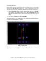
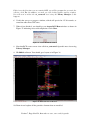
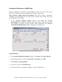
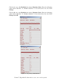
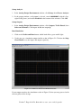
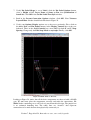
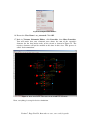
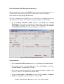
Department of Electronics and Physical Sciences
University of Surrey
Year 2 Laboratory Experiment E1
Full-Custom VLSI Design of a CMOS Inverter and a NAND
Gate Using the Cadence CAD System
User Manual
Laboratory experiments E1 and E2 will give you practical experience with using
state-of-the-art computer aided design (CAD) software. The first laboratory
session E1 will be an introduction to the Cadence CAD system using the design kit
for the austriamicrosystems (AMS) 0.35 µm complementary metal-on-silicon (CMOS)
process. Your goal is to design a CMOS inverter and NAND gate. Both designs will
be fully verified and simulated to ensure design accuracy and functionality.
The second laboratory session E2 will take the knowledge and experiences gained
during the E1 laboratory experiment and develop them further by designing a 1-bit
dynamic shift register and simulate it to demonstrate correct functionality.
Instructions for Initial Cadence Setup........................................................................2
Instructions for Normal Cadence Start Up.................................................................4
Creating and Simulating the CMOS Inverter.............................................................5
Create the CMOS Inverter Schematic....................................................................6
Functional Simulation of Inverter Gate .................................................................9
Create the CMOS Inverter Symbol......................................................................14
Generate the CMOS inverter layout ....................................................................14
Simple Rule Checks of Inverter...........................................................................24
Assura Design Rule Check (DRC) of Inverter ....................................................25
Assura Layout versus Schematic (LVS) of Inverter ............................................27
Assura Parasitic Extraction (RCX) of Inverter ....................................................28
Full Simulation With Extracted Parasitics of Inverter.........................................32
Balancing and Simulation of Inverter Gate .........................................................35
Creating and Simulating the NAND Gate ...............................................................37
Create the CMOS NAND Gate Schematic ..........................................................37
Functional Simulation of NAND Gate ................................................................39
Create the CMOS NAND Gate Symbol ..............................................................42
Generate the CMOS NAND Gate Layout ...........................................................43
Simple Rule Checks.............................................................................................51
Assura Design Rule Check (DRC) ......................................................................51
Assura Layout versus Schematic (LVS) ..............................................................52
Assura Parasitic Extraction (RCX) ......................................................................52
Full Simulation With Extracted Parasitics...........................................................55
E1 Lab Deliverables.................................................................................................58
Version 7, Page 1 of 58, Remember to save your work frequently
VLSI Design Laboratory Experiment Day 1
Instructions for Initial Cadence Setup
1.
Log into your lab terminal using your username and password.
2.
From your xterm window, prepare to run Cadence with the following command
(use tab-complete to ensure accuracy):
% source /opt/cadence/2005/scripts/ams2005.cshrc
3.
Create a directory called vlsi_lab and go into it:
% mkdir vlsi_lab
% cd vlsi_lab
4.
Start Cadence using the following command. Several windows will pop up. Do
not close any of them yet.
% ams_cds -update -tech c35b3 –mode fb
5.
Look for the Select Process Option window as shown in Figure 1, select
C35B3C1, then click OK.
Figure 1. Select Process Option Window in Cadence
6.
Look for the What’s new? window as shown in Figure 2, click File, Off at
Startup, File, then Close. (This information is for system administrators and
advanced designers)
Figure 2. What’s new? Window in Cadence
Version 7, Page 2 of 58, Remember to save your work frequently
7.
Verify that you are now left with the Library Manager window as shown in
Figure 3 and the icfb window as shown in Figure 4. You will use both of these
windows throughout the labs.
Figure 3. Library Manager Window
Figure 4. icfb Window
8.
In the Library Manager window shown in Figure 3, click File, New, then
Library. The New Library window shown in Figure 5 should appear.
Figure 5. New Library Window
9.
In the New Library window shown in Figure 5, type mylib in the Name box as
shown. Click OK.
Version 7, Page 3 of 58, Remember to save your work frequently
10.
Verify that the Technology File for New Library window appears as shown in
Figure 6 .
Figure 6. Technology File for New Library Window
11.
In the Technology File for New Library window shown in Figure 6, ensure that
Attach to an existing techfile is selected. Click OK. The Attach Design Library
to Technology File window shown in Figure 7 should appear.
Figure 7. Attach Design Library to Technology File
12.
In the Attach Design Library to Technology File window shown in Figure 7,
select TECH_C35B3 in the Technology Library pull-down. Click OK.
13.
In icfb, click File then Exit. Cadence is now set up for first use.
Instructions for Normal Cadence Start Up
If you are continuing the lab exercise from above, skip the source and cd commands
and just run the single line ams_cds –mode fb command. If you are returning to the
lab at another time, you must set up the environment again:
1. Assuming you have already logged in from your Linux or Exceed terminal, type
in the following setup command for Cadence in the xterm window:
% source /opt/cadence/2005/scripts/ams2005.cshrc
2. To start up Cadence, issue the following commands in the xterm window:
% cd vlsi_lab (if you are not already in it)
% ams_cds -mode fb
Version 7, Page 4 of 58, Remember to save your work frequently
Creating and Simulating the CMOS Inverter
The first goal of this lab is to create a CMOS inverter. Figure 8 below is an example
layout of what you will create. Now you will make your own!
LAYERS
MET1
(purple box with ‘X’
through it)
NTUB/FIMP
(clear box, orange border)
FEATURES
Vdd (power) rail
pMOS transistor
POLY1
(red hashed area)
Throughout:
PPLUS
(yellow speckled box,
yellow border)
Inverter Input
Inverter Output
NPLUS
(white speckled box,
white border)
DIFF
(green hashed area)
CONT
nMOS transistor
GND (ground) rail
(green box)
Figure 8. Example CMOS Inverter Layout
On the left hand side of the figure, each layer is labeled using the names used in this
lab. On the right hand side of the figure, the features of the inverter are labeled.
MET1: Level 1 metal, used for routing signals, vdd!, and gnd!
NTUB/FIMP: creates an n-doped region to create a p-type MOS transistor (pMOS)
(note that nearly all CMOS processes start with p-doped wafers)
POLY1: Polysilicon, used for creating transistor gates and short contacts
PPLUS: When layered with diffusion, creates transistor source and drain areas for
p-type MOS transistors (pMOS)
NPLUS: When layered with diffusion, creates transistor source and drain areas for
n-type MOS transistors (nMOS)
DIFF: Diffusion, type defined by presence of PPLUS or NPLUS
CONT: Contact, used to tie higher level 1 metal to POLY1 or DIFF layers
We could at this point continue with a full-custom layout, but there is a faster and
more accurate method. You will first design the schematic of the inverter in the
Virtuoso Schematic tool, then use the semi-custom layout tool called Virtuoso XL
to finish and verify your work, both for electrical and layout rule compliance.
Version 7, Page 5 of 58, Remember to save your work frequently
Create the CMOS Inverter Schematic
1. In the Library Manager, click once on mylib. Then click File, New, then Cell
view. The Create New File window should appear as shown in Figure 9.
Figure 9. Create New File Window
2. Ensure the Library Name is mylib. Change the Tool to Composer-Schematic
and the view name should change to schematic. Enter a Cell Name of inverter.
Click on OK. The Virtuoso Schematic Editor window should appear as shown
in Figure 10.
Figure 10. Virtuoso Schematic Editor
3. In the About What’s New window (if it appears), click Edit, Off at Startup, File,
then Close.
4. Mouse over the buttons to see the tool tips along the left side of the window. Click
on Zoom In twice.
Version 7, Page 6 of 58, Remember to save your work frequently
5. Click on the Instance button, which looks like a 10-pin IC package. A default
Add Instance window should come up as shown in Figure 11.
Figure 11. Add Instance Window
6. Click the Browse button. Select Library: PRIMLIB, Cell: nmos4, View:
symbol. The Add Instance window will expand as shown in Figure 12.
Figure 12. Expanded Add Instance Window for nmos4
7. Change the Width to the minimum size, which is 0.7u. Leave the default length
as 0.35u, which is the minimum size for our process. Do not hide the Add
Instance window, but simply place the nmos4 element somewhere below the
center of the window.
8. Similarly, place the remaining three elements from the appropriate libraries as
listed in Table 1.
Library Name
PRIMLIB
PRIMLIB
analogLib
analogLib
Table 1. Inverter Cell Components
Cell Name
nmos4
pmos4
vdd
gnd
Properties
Width=0.7u, Length=0.35u (default)
Width=0.7u, Length=0.35u (default)
9. Close the Library Select window. Hit Esc to cancel adding parts.
A few general notes on using Virtuoso. Note the “Cmd:” field at the top centre of the
window. This indicates what action will be taken with the next mouse click. You will
primarily left-click. Occasionally, commands will be nested, so use the Esc key to
clear them out or cancel the current option.
Version 7, Page 7 of 58, Remember to save your work frequently
There are various editing options too. You can Move, Stretch, and/or Copy objects
using the buttons on the left-hand side of the window. You can select first then
perform an action. Use Ctrl-d to deselect items. Note the Sel: field at the top of the
screen. It tells you how many objects are currently selected. Alternatively, you can
select an action first.
In addition, you need to learn to use the various zooming options. The quickest way to
zoom is to right-click and drag a box around an area of interest. Hit f to return to the
normal view, with the design fitted to the window. Note that you can change the zoom
level at any time without affecting your current operation.
10. Now, wire everything up using the Wire (narrow) button. Hit Esc to cancel any
action. Click Delete or Undo to correct mistakes.
11. Finally, add an input pin called A using the Pin button. Hit Enter to place the pin.
12. Similarly, make an output pin called Q.
13. Click the Check and Save button when you are finished.
14. Check for errors in the icfb window.
15. Verify that your schematic looks similar to the one in Figure 13. Do not close the
Virtuoso Schematic Editor until told to do so.
Figure 13. Inverter Schematic
Version 7, Page 8 of 58, Remember to save your work frequently
Functional Simulation of Inverter Gate
Having completed the schematic of the inverter the next stage of the design process is
to simulate its basic functionality to check for design errors. You will be using
Cadence’s implementation of the industry standard spice simulator called Spectre. If
you are familiar with spice, then you will probably remember generating spice
extractions, netlists, and simulation files. Cadence has neatly integrated all these
functions for us in one package, so we do not have to do any text editing. Of course,
you can do it the old-fashioned way, but we are not going to in this lab.
Start Virtuoso Analog Design Environment: The goal of doing a functional
simulation of your inverter gate is to ensure that you wired it up correctly. The setup
for simulation is fairly simple.
1. In the Virtuoso Schematic Editor window, click Tools, then Analog
Environment. The analog environment will open another schematic view and
will probably re-organize all your windows. Most importantly, the Virtuoso
Analog Design Environment window will pop up as in Figure 14.
Figure 14. Virtuoso Analog Design Environment
Setup simulation:
1. In the Analog Design Environment window, click Setup, then Choose Design.
2. In the popup window, verify the View Name is schematic. Click OK.
3. In the Analog Design Environment window, click Setup, then Setup Stimuli.
You should get a rather long window pop up as shown in Figure 15.
Version 7, Page 9 of 58, Remember to save your work frequently
4. In the Setup Analog Stimuli window, verify Stimulus Type is set to Inputs and
click on the first line that says OFF A/gnd! Voltage dc.
5. Change function to pulse. Click Enabled, Set the first 10 parameters to: 3.3,
<blank>, 0.0, 0.0, 3.3, 1ns, 0.1ns, 0.1ns, 1ns, 2ns as shown in Figure 15.
6. Click Change to set values.
Figure 15. Setup Analog Stimuli Window
Version 7, Page 10 of 58, Remember to save your work frequently
7. Still in the Setup Analog Stimuli window, click on Global Sources.
8. Verify Function is dc. Click Enabled. Enter DC voltage of 3.3. Click Change.
9. Click OK to close the Setup Analog Stimuli window.
Setup Analysis:
1. In the Analog Design Environment window, click Analyses, then Choose.
2. In the popup window, ensure tran is selected, enter 0.000000003 (which is 3ns,
eight leading zeros) and click Enabled at the bottom of the window. Click OK to
close the popup window.
Setup Outputs:
1. In the Analog Design Environment window, click Outputs, To Be Plotted, then
Select on Schematic. Click input A then output Q in the Virtuoso Schematic
Editor. Your Analog Design Environment should now look like that in Figure
16.
One element that has not been included is a device load. Normally, one would create
a test bench that would include a device, an inverter in our case, driving another
device or capacitive load. However, this is a functional simulation so no load will be
needed.
Figure 16. Analog Design Environment Ready for Simulation
Version 7, Page 11 of 58, Remember to save your work frequently
Run Simulation:
1. In the Analog Design Environment window, click on the Netlist and Run button,
which looks like a green traffic light.
2. Verify you get a Welcome to Spectre window. The only important message for
us is #5, indicating that we need to be sure and save our schematic and layout
views before proceeding. Do so now then return to this window. Click Do not
show this text again at the bottom of the window then click OK.
3. Verify that you soon get a log file and simulation window. If you have made an
error in setting up the simulation, you will only get a log file reporting what the
problem is. Most likely, you need to re-verify your work from the last three pages.
4. Review the log file. You will get a few warnings (approximately 42, check total at
bottom) about inline components, which can be ignored for our exercise. There
should be a few notices (approximately 3, check total at bottom). These are
because we are simulating such a small device and some of the parameters seem
very small to the simulator.
5. Click File then Close Window when you are finished reviewing the log file.
6. Verify you get a simulation results graph as shown in Figure 17. If your output
matches the simulation results in Figure 17 then you may proceed with the lab.
Figure 17. Inverter Functional Simulation Results
Version 7, Page 12 of 58, Remember to save your work frequently
Save Simulation Results:
1. In the Analog Design Environment window, save your simulation results by
clicking Session then Save State.
2. Use the name of functional for the session as shown in Figure 18.
3. Click OK when finished.
Figure 18. Saving Functional Simulation Results
4. Click Session, Quit in the Analog Design Environment window.
Version 7, Page 13 of 58, Remember to save your work frequently
Create the CMOS Inverter Symbol
1. In the Virtuoso Schematic Editor, click on Design, Create Cellview, then From
Cellview.
2. Click OK in the Cellview From Cellview window that pops up without making
any changes.
3. Click OK in the following Symbol Generation Options window.
4. Use the simple drawing commands to make an inverter symbol as shown in Figure
19. Use Add, then Shape for objects such as circles.
5. Save the design and close the symbol window when finished.
Figure 19. Inverter Symbol
Generate the CMOS inverter layout
1. In the Virtuoso Schematic Editor window showing your inverter schematic,
click Tools, Design Synthesis, then Layout XL.
2. Click OK in the Startup Option window, keeping the Create New setting.
3. Click OK in the Create New File window, accepting all defaults. A new
Virtuoso Layout Editor window will appear, which will be empty, along with a
slim LSW (Layer Selection Window).
4. In the About What’s New window (if it appears), click Edit, Off at Startup, File,
then Close.
Version 7, Page 14 of 58, Remember to save your work frequently
Just a few notes before we continue. Everything in Cadence is measured in
micrometers (µ, which is 10-6 meters). You will start off with a “minimum-sized”
design. This means that the gate length, which is the distance from the source to the
drain, is the minimum size for the technology, which in this case is 0.35µ. Typically,
for any technology, you want the length to be the minimum size, allowing for tighter
packing density of cells.
The gate width is the other dimension, which determines the drive strength—i.e. the
wider the gate, the more downstream devices can be driven, which is called fanout.
The ratio is typically 1:4. The minimum width for this technology is 0.70µ.
5. In the Virtuoso Layout Editor window, note that the dots on the screen are
spaced at 1.0µ intervals and that the mouse snaps to grid points at 0.1µ intervals.
However, this spacing will not work for us, as we will need 0.025µ spacing to
work with minimum-sized features.
6. Click on Options, then Display. You should get a Display Options window as
shown in Figure 20.
Figure 20. Display Options Window
Version 7, Page 15 of 58, Remember to save your work frequently
7. In the Display Options window, click on the Axes, Nets, and Pin Names buttons
in the Display Controls box so they are darkened. Then, in the Grid Controls
box, enter 0.025 for both X and Y Snap Spacing. Change only the Edit Snap
Mode to anyAngle as shown in Figure 20.
8. Click OK to close the Display Options window.
9. In the Virtuoso Layout Editor window, click on Design then Gen From Source.
A Layout Generation Options window will appear as shown in Figure 21.
Figure 21. Layout Generation Options Window
It is very important that you perform the next few steps correctly!
10. In the middle of the Layout Generation Options window shown in Figure 21,
click on the A row terminal. Hold down shift and click the Q row. Below the
terminal box, change the Pin Type to Geometric then Layer/Master to MET2
(pn). Click Update.
11. Similarly, select “gnd!” and “vdd!” and set the Layer to MET1 (pn), but change
the width and height to 1.0 before clicking Update.
12. Finally, ensure Pin Label Shape is set to Label, click the Pin Label Options
button, select a Height of 0.5, Layer Name of Same as Pin, then Justification of
lowerLeft. Click OK to close the Set Pin Label Text Style window.
Version 7, Page 16 of 58, Remember to save your work frequently
13. Back in the Layout Generation Options window, click OK. Your Virtuoso
Layout Editor window should look like that in Figure 22.
Figure 22. Initial Virtuoso XL View
Looking at Figure 22, notice that all the basic components are there to build an
inverter. We must now place the components correctly and add make the connections.
The purple box is an estimated bounding box. The white lines are “airwires” that
represent connections to be made that not been physically connected yet.
14. Hit Shift-f before continuing to see all levels of your hierarchical design.
Version 7, Page 17 of 58, Remember to save your work frequently
Perform initial placement:
1. Click Edit then Place as in Schematic. Click Yes in the confirmation popup
window. All components will be placed similar to the arrangement in the
schematic.
2. Click Window then Fit All.
3. Click Zoom Out once. You should be able to see Y=16. Use the Stretch button to
move the top of the bounding box to Y=16 exactly, by entering 0:16 in icfb to
place it exactly. Note that throughout this lab the instruction will call for entering
coordinates in icfb to ensure design rules are met.
4. Click Esc to cancel stretching.
Create Power and Ground rails:
Creating “standard cells” that have a common height is a convenient design choice, as
you will be able to place the inverter, and the other cells you will create later in the
lab, side by side without any further modifications. Additionally, standard cells can be
used in a fully automated “place and route” to generate very large designs. The
tradeoff is a penalty in area, as each cell will not be as small as it could feasibly be.
1. Select MET1(drw) in LSW.
2. Draw two rectangles using the Rectangle command with the following
coordinates: 0:0 to 9:2 and 0:14 to 9:16 (remember to enter them in icfb to make
it exact).
3. Cancel rectangle mode with Esc.
4. Click Move.
5. Click exactly on the lower left-hand corner of the gnd! box. Move it exactly to
0:0. You may need to zoom in and out to do this (remember a quick way to zoom
in on an area of interest is to drag a box using a right-click over an area—then hit f
to fit design again).
6. Hit Ctrl-d to deselect the object.
7. Now Stretch the upper right-hand corner of the gnd! box to exactly 9:2. Your pin
label must overlap the MET1(drw) box exactly or you will get design errors later.
8. Repeat this process for the vdd! pin label with the previous dimensions of 0:14 to
9:16. Your work should like that in Figure 23.
Version 7, Page 18 of 58, Remember to save your work frequently
Figure 23. vdd! and gnd! Rails Drawn and Labeled
Place pMOS device and expand NTUB (nwell):
Although not immediately apparent, the pMOS device needs flipped end-over-end,
which is called “permutation” in Virtuoso.
1. With nothing selected (Ctrl-d), click Move, then click exactly on the upper lefthand corner of the NTUB of the pMOS device (zoom in needed). Holding down
Shift, right-click, then release Shift. (you may have to repeat right clicking until
you are holding it by the lower left-hand corner) This action flipped the device
over. Place the device exactly at 3:9.
2. Click FIMP in LSW.
3. Draw a FIMP Rectangle from 0:9 to 9:16.
4. Repeat the two previous steps to create an NTUB Rectangle.
Place nMOS device:
1. With nothing selected (Ctrl-d), click Move, then click exactly on the lower lefthand corner of the outline box of the nMOS device (zoom in needed). Place
exactly at 3.8:3.
2. Verify that you have what is shown in Figure 24. Although the transistor gates
appear to have a crossed connection, they really do not, as you will see soon…
Version 7, Page 19 of 58, Remember to save your work frequently
Figure 24. Placed nMOS and pMOS Devices
Now we must replace some of the airwires with metal connections. To eliminate
confusion between “nets” and “unconnected nets,” we must turn off the “nets.”
1. Click Options, Display, deselect Nets, then OK.
2. Click Connectivity, Show Incomplete Nets, Select All, then OK. Your Virtuoso
display will now be colored with areas represented unconnected nets. We will fix
this now.
Make vdd! and gnd! connections:
1. Click the Path button.
2. Click in the middle of the source contact (top one) of the pMOS device. You may
want to Hide Incomplete Nets first.
3. When prompted, choose the MET1 layer then OK.
4. Move the mouse up until you are well within the vdd! rail.
5. DO NOT click, but hit Enter to complete the trace. The unconnected net
indication should disappear.
6. Repeat this process for the nMOS drain to gnd! connection.
Version 7, Page 20 of 58, Remember to save your work frequently
Make the device output connection (Q):
1. Using Move, click exactly on the lower left-hand corner of the Q contact and
place at 7:4.65.
2. Click Path. We now need to connect the pMOS drain to the nMOS source then to
the Q pin, but it is a bit tricky to do this.
3. Click on the pMOS drain.
4. When prompted, choose the MET1 layer then OK.
5. Click on the nMOS source.
6. Hit F3 to bring up the Create Path window. Near Change to Layer, select
MET2(dg) (same as MET2(drw) in LSW).
7. Back in the Virtuoso Layout window, hit Enter over the Q pin. A via from
MET1 to MET2 will be automatically created and placed. The unconnected net
indication should go away.
Make the device input connection (A):
1. Move pin A to 1:4.
2. Click Path.
3. Connect the pMOS gate to the nMOS gate on the left side, refer to Figure 25 if
needed.
4. Hit Enter to finish.
5. Still in Path mode, click the nMOS gate, move to the left a bit then change the
path layer using F3 to MET1(dg).
6. Click right between the starting point and the A pin, which will drop a POLY1(dg)
to MET1(dg) contact.
7. Change the layer to MET2(dg) then hit Enter over the A pin. All incomplete net
indications should disappear.
8. Verify that your design looks similar to that in Figure 25.
Version 7, Page 21 of 58, Remember to save your work frequently
Figure 25. A and Q Connections Made
Create body tie for pMOS:
We now need to connect vdd! to the NTUB (nwell). You will get a “hot nwell” error
later if you do not, in addition to the device not operating properly.
1. Click Create then Contact.
2. Set the Contact Type to ND_C (this may seem opposite to what you might think,
but remember the vdd! needs tied to the NTUB, so an n-type diffusion contact is
needed).
3. Place 3 contacts evenly spaced in the vdd! region.
Create body tie for nMOS:
We now need to connect gnd! to the substrate (the wafer).
1. Set the Contact Type to PD_C.
2. Place 3 contacts evenly spaced in the gnd! region.
Version 7, Page 22 of 58, Remember to save your work frequently
Change pin label layers:
Before moving on to more detailed design rule checks using Assura, we must modify
the layer of the vdd!, gnd!, A, and Q pin labels, or we will get unexpected errors. The
only tricky part of this step is ensuring you select the label and not the nearby metal.
1. Using the Properties button, change the vdd! and gnd! label layer to PIN(M1).
You will know that you have selected the pin when the Properties text field
shows the label you were trying to select. You may have to right-click to get it to
appear.
2. Then, change the A and Q pin labels to PIN(M2).
Your inverter design is now complete, if you have followed the instructions properly.
It should look similar to the one in Figure 26.
Figure 26. Inverter Layout
To make sure your design is good, we will now step through a series of design rule
checks.
Version 7, Page 23 of 58, Remember to save your work frequently
Simple Rule Checks of Inverter
Before we can declare success, you must now ensure that your work is error-free.
There are a number of tools to do this.
Simple check of design integrity:
1. Click Connectivity, Check, then Shorts and Opens.
2. Verify you get an error-free report as shown in Figure 27. If not, go back, correct
your design now, and re-check.
Figure 27. Simple Check of Shorts and Opens
3. Next, click Connectivity, Check, then Against Source. This checks the layout
versus the schematic.
4. Verify you get an error-free report as shown in Figure 28. Ignore the two
warnings about terminal B. We made these connections manually. If you have
other errors, go back, correct your design now, and re-check.
Figure 28. Simple Check of Layout vs. Schematic
Version 7, Page 24 of 58, Remember to save your work frequently
Assura Design Rule Check (DRC) of Inverter
Run Assura DRC:
1. Click Assura, then Run DRC.
2. Verify you get a window like that in Figure 29. A Save Cellviews window may
pop up, click OK if it does.
Figure 29. Run Assura DRC Window
3. Click on Set Switches. You should get a window like that in Figure 30.
4. Click on no_generated_layers.
5. Hold the Ctrl key down and click no_coverage. This will keep the DRC from
reporting errors that are only used for processing a final design for fabrication.
6. Click OK in the Set Switches window.
Figure 30. Set Switches Window
7. In the Run Assura DRC window, click OK. An Overwrite Existing Data
Window maypop-up, but only if you have run the DRC before, click OK.
8. Verify that a Progress window briefly comesup—just wait for it to go away.
Version 7, Page 25 of 58, Remember to save your work frequently
9. Verify that an inverter has completed SUCCESSFULLY! window will pop up.
10. Click Yes to view the results. If you have done everything correctly, you should
get a No DRC errors found window as in Figure 31.
Figure 31. No DRC errors found Window
However, if you do get an Error Layer Window, you will need to fix your errors.
For example, if you have a spacing error, you might get something like in Figure 32.
The colored box to the left of the error message tells you where to look for the error in
your design. If you click on the message in the right hand column, it will zoom in to
the error in the Virtuoso Layout Editor. The error will be seen as a flashing polygon
or large ‘X.’ To fix the error, use the Ruler button to map out the correct spacing.
Then correct using a Move or Stretch command.
11. When you are ready to proceed, click Assura, then Close Run. Repeat this
process until your design is error free.
Figure 32. Error Layer Window
Version 7, Page 26 of 58, Remember to save your work frequently
Assura Layout versus Schematic (LVS) of Inverter
Run Assura LVS:
1. Click Assura, then Run LVS. You should get a window like that in Figure 29. If
you are asked to save the design first, choose Yes.
Figure 33. Run Assura LVS Window
2. Click OK in the Run Assura LVS window. An Overwrite Existing Data
Window maypop-up, but only if you have run the DRC before, click OK.
3. Verify that a Progress window briefly comes up—just wait for it to go away.
4. Verify that a Run: inverter Schematic and Layout Match window pops up.
Click Yes to view the results.
5. Verify that you get a No DRC errors found window as in Figure 34. Click Close.
Figure 34. No DRC errors found Window
6. Verify that the schematic pops up with an LVS Debug-inverter window as in
Figure 35.
If you have any errors, you will need some help in sorting it out, as you should not
have had any errors if the directions were followed. You can click on the error and
use the Open Tool option for help in fixing it.
Version 7, Page 27 of 58, Remember to save your work frequently
Figure 35. Schematic and Layout Match Window
Assura Parasitic Extraction (RCX) of Inverter
As you know, the device you have created has resistive and capacitive parasitic
elements. Before we move on to the next phase of our work, which is device
simulation, we need the most accurate model of our inverter device as possible.
Run Assura RCX:
1. Click Assura, then Run RCX.
2. Click on the Extraction tab. You should get a window like that in Figure 36.
Figure 36. Run Assura RCX Window
3. Change Extraction Mode to RC.
4. Enter gnd! in Ref Node.
5. Click OK.
Version 7, Page 28 of 58, Remember to save your work frequently
If this is not the first time you are running RCX, you will be prompted to overwrite the
cellview, click Yes. In addition, you may get a file locking failure and log window.
You will need to delete the av_extracted view using the Library Manager if this
happens.
6. Verify that you get a progress window, which will persist for 15-30 seconds, as
extraction takes more CPU time.
7. When it has finished, you should get an Assura RCX Run window as shown in
Figure 37 indicating successful completion. Click Close.
Figure 37. Assura RCX Run Window
8. Note that RCX creates a new view called av_extracted. Open this new view using
Library Manager.
9. Hit Shift-f to flatten. You should get a layout as in Figure 38.
Figure 38. Extracted View of Inverter
10. Zoom in and explore all the parasitic elements that are modeled.
Version 7, Page 29 of 58, Remember to save your work frequently
11. To make the view even more interesting, enable Nets in Options, Display. Data
shown in this view will be used to simulate the performance of the device.
12. Click Window, Close when you are finished viewing the results.
13. Back in the regular view of the inverter in the Virtuoso Layout Editor window,
click Assura, then Close Run. Remember to leave the layout and schematic views
open throughout the development of the inverter.
14. In the Virtuoso Schematic Editor, click Tools, then Parasitics. You should get a
Parasitics menu choice.
15. Click Parasitics, then Setup. The Setup Parasitics window shown in Figure 39
should pop up.
Figure 39. Setup Parasitics Window
16. Ensure the View Name is av_extracted. Click OK.
17. Back in Virtuoso Schematic Editor, click Parasitics, then Show Parasitics. You
will notice that your schematic now shows the sum of the capacitive elements for
the four major nodes of the circuit as shown in Figure 40. The resistive elements
will not be enabled at this time in this view. This process is called “back
annotation.”
Version 7, Page 30 of 58, Remember to save your work frequently
Figure 40. Back Annotation of Parasitics in the Inverter Schematic
Now, everything is set up for device simulation.
Version 7, Page 31 of 58, Remember to save your work frequently
Full Simulation With Extracted Parasitics of Inverter
Having completed the layout of the inverter the next stage of the design process is to
simulate the operation and investigate rise and fall times of the inverter.
Start Virtuoso Analog Design Environment:
The goal of simulating our inverter gate is to ensure that it is working properly and
that it performs the way we want it to. The setup for simulation is fairly simple.
1. In the Virtuoso Schematic Editor window, click Tools, then Analog
Environment. The analog environment will open another schematic view and
will probably re-organize all your windows. Most importantly, the Virtuoso
Analog Design Environment window will pop up as in Figure 41.
Figure 41. Virtuoso Analog Design Environment
Setup simulation:
1. In the Analog Design Environment window, click Setup, then Choose Design.
2. In the popup window, change the View Name to av_extracted. Click OK.
3. Since you have already entered the desired stimuli and points to graph in the
previous simulation, click Session, then Load State.
4. Verify the State Name is functional and select ONLY Analyses, Graphical
Stimuli, and Outputs as shown in Figure 42. Click on OK.
Version 7, Page 32 of 58, Remember to save your work frequently
Figure 42. Setup Analog Stimuli Window
5. Verify that your Analog Design Environment looks like that in Figure 43.
Note: One element that has not been included is a device load. Normally, one would
create a test bench that would include a device, an inverter in our case, driving
another device or capacitive load. However, the parasitic load in the device itself will
be enough for this demonstration.
Figure 43. Analog Design Environment Ready for Simulation
6. Click on the Netlist and Run button, which looks like a green traffic light.
Version 7, Page 33 of 58, Remember to save your work frequently
You should soon get a log file and simulation window. First, review the log file. You
will get a few warnings (approximately 42, check total at bottom) about inline
components, which can be ignored for our exercise. There should be a few notices
(approximately 10, check total at bottom). These are because we are simulating such a
small device and some of the parameters seem very small to the simulator.
7. Click File then Close Window when you are finished reviewing the log file.
8. Verify that you get a simulation results graph as shown in Figure 44.
Figure 44. Initial Inverter Simulation Results
Your task is now to determine tr, tf, tpHL and tpLH. You should already be familiar with
which points to measure these between on the simulation output curves. There are
several ways to do this using the Cadence simulation results window. Click Trace
then Trace Cursor to manually compute the four results needed. Trace then Delta
Cursor can be used as well. Additionally, you can use Maker, Place, then Trace
Marker (or just hit t then click where you want a label).
Figure 45. Initial Inverter Simulation Results with tr, tf, tpHL & tpLH labeled
9. When you are finished, in the Virtuoso Analog Design Environment window,
click Session then Save State as full. Do not close your session!
Version 7, Page 34 of 58, Remember to save your work frequently
Balancing and Simulation of Inverter Gate
What you should have noticed right away was that the delay, fall, and rise times are
not balanced. Typically, you want the delay times to match, and get the fall and rise
times as close as possible. Fortunately, there are some tools that we can use to
simplify the job. Recalling that we used standard parameterized “pcells” for the
nMOS and pMOS devices, we can just change the gate width of one of the
appropriate device and re-simulate. You should already know from your studies that
pMOS devices are typically sized 3X larger than nMOS devices in width. Typically,
you will always want your gate length to be the minimum size.
Change the gate width in schematic:
1. In the Virtuoso Schematic Editor, click on the Properties button then click on
the pMOS device.
2. Change the gate width to 2.1u (3X minimum).
3. Click OK in Edit Object Properties.
4. Click the Check and Save button.
Change gate width in layout:
1. In the Virtuoso Layout Editor, click Tools, then Layout XL.
2. Click Connectivity, Update, Layout Parameters (not Schematic Parameters).
You should get a Virtuoso XL Info similar to the one in Figure 46.
Figure 46. Virtuoso XL Info Reporting Schematic Parameters Updating Layout Parameters
1. Click File, then Close Window.
2. Examine the Virtuoso Layout Editor. You should notice that your pMOS device
was adjusted in size. Look closely to see if any metal traces need modified to meet
design rules (i.e. there should be no small notches). Make changes if necessary
then Save the updated layout.
Version 7, Page 35 of 58, Remember to save your work frequently
Re-run Assura verification tools:
1. Re-run Assura DRC, LVS, and RCX using the same procedure as before. Do not
forget to change the Extraction Mode to RC. You may get a file locking error
during RCX—if you do, try to run RCX again, otherwise, use Library Manager
and delete the av_extracted view and try RCX again.
2. Click Assura, then Close Run when your design passes all three checks.
Re-run simulation:
1. In the Virtuoso Analog Design Environment, click the green stoplight Netlist
and Run. You will get a new simulation results window. At first, it may seem to
be the same as before, but after you make your measurements again, you will
notice that the output has changed slightly.
2. Your tpHL and tpLH should be within 0.010ns of each other and tr and tf are as
close as possible.
3. Save your final simulation state as balanced.
4. Before your close your windows, check on the last page of these instructions to
see what deliverables are required from you. You will need to use Alt-PrintScrn
and put your screen snapshots into something like OpenWindows Writer so you
can print. Make sure you select the printer that is in the lab room.
5. Save all other work and close all inverter windows when complete.
Version 7, Page 36 of 58, Remember to save your work frequently
Creating and Simulating the NAND Gate
To be able to construct the 1-bit shift register you will need two more components in
addition to the inverter you have just designed. These additional components are the
NAND gate and the pass gate (also called a transmission gate). You will complete the
transmission gate at the beginning of the E2 lab. For these two devices, you will use
the same pMOS/nMOS sizing ratio you found previously.
Note: the following instructions are similar to those of the inverter gate, but have
been abbreviated slightly where possible.
Create the CMOS NAND Gate Schematic
1. In the Library Manager, click once on mylib. Then click File, New, then
Cellview. The Create New File window should appear as shown in Figure 47.
Figure 47. Create New File Window
2. Verify the Library Name is mylib. Change the Tool to Composer-Schematic
and the view name should change to schematic. Enter a Cell Name of nand.
Click on OK. The Virtuoso Schematic Editor window should appear.
3. Click on Zoom In twice.
4. Click on the Instance button, which looks like a 10-pin IC package. A default
Add Instance window should come up.
5. Click the Browse button. Select Library: PRIMLIB, Cell: nmos4, View:
symbol. The Add Instance window will expand.
6. Change the Width to the minimum value of 0.7u. Leave the default length as
0.35u, which is the minimum size for our process. Do not hide the Add Instance
window, but simply place the nmos4 elements (you need 2) somewhere below the
center of the window.
7. Similarly, place the remaining elements from the appropriate libraries as listed in
Table 2. Make sure you set the pMOS width to 2.1u.
Version 7, Page 37 of 58, Remember to save your work frequently
Library Name
PRIMLIB
PRIMLIB
analogLib
analogLib
Table 2. NAND Cell Components
Cell Name
nmos4 (quantity 2)
pmos4 (quantity 2)
vdd
gnd
Properties
Width=0.7u, Length=0.35u (default)
Width=2.1u, Length=0.35u (default)
8. Close the Library Select window. Hit Esc to cancel adding parts.
9. Now, wire everything up using the Wire (narrow) button. Hit Esc to cancel any
action. Click Delete or Undo to correct mistakes.
10. Finally, add an input pin called A using the Pin button. Hit Enter to place the pin.
11. Repeat for input B. You may use multiple pins to make the design cleaner if you
would like.
12. Similarly, make an output pin called Q.
13. Click the Check and Save button when you are finished.
14. Check for errors in the icfb window.
15. Verify that your schematic looks similar to the one in Figure 48. You will leave
the Virtuoso Schematic Editor open for the remainder of the lab.
Figure 48. NAND Schematic
Version 7, Page 38 of 58, Remember to save your work frequently
Functional Simulation of NAND Gate
Having completed the schematic of the NAND gate, the next stage of the design
process is to simulate its basic functionality to check for design errors.
Start Virtuoso Analog Design Environment: The goal of doing a functional
simulation of your NAND gate is to ensure that you wired it up correctly. The setup
for simulation is fairly simple.
1. In the Virtuoso Schematic Editor window, click Tools, then Analog
Environment. The analog environment will open another schematic view and
will probably re-organize all your windows. Most importantly, the Virtuoso
Analog Design Environment window will pop up as in Figure 49.
Figure 49. Virtuoso Analog Design Environment
Setup simulation:
1. In the Analog Design Environment window, click Setup, then Choose Design.
2. In the popup window, verify the View Name is schematic. Click OK.
3. Click Setup, then Setup Stimuli.
4. As before, create a 3.3V global source.
5. Now you will have two inputs to configure as shown in Figure 50.
Version 7, Page 39 of 58, Remember to save your work frequently
Click the A row, click Enabled then choose Function: Pulse. Enter the following
values for the 10 fields: 3.3, <blank>, 0.0, 0.0, 3.3, 1ns, 0.1ns, 0.1ns, 1ns, 2ns. Click
Change.
Click the B row, click Enabled then choose Function: Pulse. Enter the following
values for the 10 fields: 3.3, <blank>, 0.0, 0.0, 3.3, 2ns, 0.1ns, 0.1ns, 2ns, 4ns. Click
Change then OK.
Figure 50. Setup Analog Stimuli Window
Version 7, Page 40 of 58, Remember to save your work frequently
Setup Analysis:
1. In the Analog Design Environment window, click Setup, then Choose Analyses.
2. In the popup window, verify tran is selected, enter 0.000000005 (which is 5ns,
eight leading zeros) and enable Enabled at the bottom of the window. Click OK.
Setup Outputs:
1. In the Analog Design Environment window, click Outputs, To Be Plotted, then
Select on Schematic. Click inputs A, B, then output Q.
Run Simulation:
1. Click on the Netlist and Run button, which looks like a green traffic light.
2. Verify you get a simulation output similar to that in Figure 51. Click on the Strip
Chart Mode to see the inputs and output separately.
Figure 51. NAND Gate Functional Simulation Results
If your output matches the simulation results in Figure 51 then you may proceed with
the next phase of the design.
Version 7, Page 41 of 58, Remember to save your work frequently
Save Simulation Results:
1. In the Analog Design Environment window, click Session then Save State in the
Analog Design Environment window.
2. Use the name of functional for the session. Click OK when finished.
3. Then click Session, Quit in the Analog Design Environment window.
Create the CMOS NAND Gate Symbol
1. In the Virtuoso Schematic Editor, click on Design, Create Cellview, then From
Cellview.
2. Click OK in the Cellview From Cellview window that pops up without making
any changes.
3. In the pop-up Symbol Generation Options window, eliminate duplicate A and B
entries then click OK.
4. Use the simple drawing commands to make a NAND symbol as shown in Figure
52. Use Add, then Shape for objects such as circles.
5. Save the design and close the symbol window when finished.
Figure 52. NAND Symbol
Version 7, Page 42 of 58, Remember to save your work frequently
Generate the CMOS NAND Gate Layout
1. In the Virtuoso Schematic Editor window showing your NAND schematic, click
Tools, Design Synthesis, then Layout XL.
2. Click OK in the Startup Option window, keeping the Create New setting.
3. Click OK in the Create New File window, accepting all defaults. A new
Virtuoso Layout Editor window will appear, which will be empty.
4. In the Virtuoso Layout Editor window, click on Design then Gen From Source.
A Layout Generation Options window will appear as shown in Figure 53.
Figure 53. Layout Generation Options Window
It is very important that you perform the next few steps correctly!
5. In the middle of the Layout Generation Options window shown in Figure 53,
click on the A row terminal. Hold down shift and click the Q row (selecting the A,
B, and Q rows). Below the terminal box, change the Pin Type to Geometric then
Layer/Master to MET2 (pn). Click Update.
6. Similarly, select “gnd!” and “vdd!” and set the Layer to MET1 (pn), but change
the width and height to 1.0 before clicking Update.
Version 7, Page 43 of 58, Remember to save your work frequently
7. Verify Pin Label Shape is set to Label, click the Pin Label Options button,
select a Height of 0.5, Layer Name of Same as Pin, then Justification of
lowerLeft. Click OK in the Set Pin Label Text Style window.
8. Back in the Layout Generation Options window, click OK. Your Virtuoso
Layout Editor window should look like that in Figure 54.
9. Verify your Options, Display options are as they were previously: First, click on
the Axes, Nets, and Pin Names buttons in the Display Controls box so they are
darkened. Then, in the Grid Controls box, enter 0.025 for both X and Y Snap
Spacing. Change only the Edit Snap Mode to anyAngle. Finally, click OK.
Figure 54. Initial Virtuoso XL View
Looking at Figure 54, notice that all the basic components are there to build a NAND
gate. We must now place the components correctly and make the connections. Hit
Shift-f before continuing to see all levels of your hierarchical design. The purple box
is an estimated bounding box. The white lines are “airwires” that represent
connections to be made that not been physically connected yet.
Version 7, Page 44 of 58, Remember to save your work frequently
Perform initial placement:
1. Click Edit then Place as in Schematic. Click Yes in the confirmation popup
window. All components will be placed similar to the arrangement in the
schematic.
2. Click Window then Fit All.
3. Click Zoom Out once. You should be able to see Y=16. Use the Stretch button to
move the top of the bounding box to Y=16 exactly, by entering 0:16 in icfb to
place it exactly. Then move the right side of the box to X=9 exactly.
4. Click Esc to cancel stretching.
Create Power and Ground rails:
1. Select MET1(drw) in LSW.
2. Draw two rectangles using the Rectangle command with the following
coordinates: 0:0 to 9:2 and 0:14 to 9:16 (remember to enter them in icfb to make
it exact).
3. Cancel rectangle mode with Esc.
4. Click Move.
5. Click exactly on the lower left-hand corner of the gnd! box. Move it exactly to
0:0. You may need to zoom in and out to do this (remember a quick way to zoom
in on an area of interest is to drag a box using a right-click over an area—then hit f
to fit design again).
6. Hit Ctrl-d to deselect the object.
7. Now Stretch the upper right-hand corner of the gnd! box to exactly 9:2. Your pin
label must overlap the MET1(drw) box exactly or you will get design errors later.
8. Repeat this process for the vdd! pin label with the previous dimensions of 0:14 to
9:16. Your work should like that in Figure 55.
Version 7, Page 45 of 58, Remember to save your work frequently
Figure 55. vdd! and gnd! Rails Drawn and Labeled
Place pMOS devices and expand NTUB (nwell):
Since you have two pMOS devices that share some common connections, you can
overlap the contacts. But be careful when doing this, you want to overlap the contacts
that are tied together, going on to the output and nMOS devices. They will also need
rotated 90 degrees from their original placement. If you do this properly, your
“outside” non-overlapped contacts will be tied each to vdd!
1. Place the bottom edge of the NTUB area of the overlapped pMOS devices at Y=9,
roughly centered.
2. Now draw a FIMP and NTUB Rectangle from 0:9 to 9:16. Be sure to select them
in the LSW before drawing. These layers are needed to create the pMOS device.
Place nMOS devices:
1. Click Ctrl-d. Likewise, you can overlap contacts on the nMOS devices. When
you do this, you will note this time that the common contact disappears. You will
have to rotate your devices 90 degrees. Watch your airwires and be sure you have
the right nMOS device under the corresponding pMOS device above.
2. Verify you have what is shown in Figure 56.
Version 7, Page 46 of 58, Remember to save your work frequently
Figure 56. Placed nMOS and pMOS Devices
Now we must replace some of the airwires with metal connections. First, to eliminate
the confusion between “nets” and “unconnected nets,” we must turn off the “nets.”
1. Click Options, Display, deselect Nets, then OK.
2. Click Connectivity, Show Incomplete Nets, Select All, then OK. Your Virtuoso
display will now be colored with areas represented unconnected nets.
Make vdd! and gnd! connections:
1. Click the Path button.
2. Click in the middle of the source contact (top one) of the left pMOS device. You
may want to Hide Incomplete Nets first.
3. When prompted, choose the MET1 layer then OK.
4. Move the mouse up until you are well within the vdd! rail.
5. DO NOT click, but hit Enter to complete the trace. The unconnected net
indication should disappear.
6. Repeat this process for the other pMOS device and nMOS to gnd! connections.
Version 7, Page 47 of 58, Remember to save your work frequently
Make the device output connection (Q):
1. Using Move, click exactly on the lower left-hand corner of the Q contact and
place at 0.7:8.
2. Click Path. We now need to connect the overlapped pMOS contacts to the
appropriate nMOS contact then to the Q pin, but it is a bit tricky to do this.
3. Click on the pMOS overlapped contacts.
4. When prompted, choose the MET1 layer then OK.
5. Bring the metal down to about Y=8.3, then click and move toward the Q pin.
6. Hit F3 to bring up the Create Path window. Near Change to Layer, select
MET2(dg) (same as MET2(drw) in LSW).
7. Back in the Virtuoso Layout window, hit Enter over the Q pin. A via from
MET1 to MET2 will be automatically created and placed. Some of the
unconnected net indication should go away.
8. Complete the path by making a path from the appropriate nMOS contact to the
existing MET1 path.
Make the device input connection (A):
1. Move pin A to about 0.5:6.4.
2. Move pin B to 6:6.9.
3. Click Path.
4. Connect the appropriate pMOS gate to the nMOS gate with POLY1(dg).
5. Hit Enter to finish.
6. Repeat for the other pair. (on the left side, hit Enter to finish).
7. Connect the POLY1(dg) areas to the A or B pin, as appropriate, by using the F3
options to change to MET1(dg), drop a via, then change again to MET2(dg)
then hit Enter over the appropriate pin. Keep in mind the space rule violations
from before. All incomplete net indications should disappear.
8. Verify that your design should look similar to that in Figure 57.
Version 7, Page 48 of 58, Remember to save your work frequently
Figure 57. A, B, and Q Connections Made
Create body tie for pMOS:
We now need to connect vdd! to the NTUB (nwell). You will get a “hot nwell” error
later if you do not, in addition to the device not operating properly.
1. Click Create then Contact.
2. Set the Contact Type to ND_C (this may seem opposite to what you might think,
but remember the vdd! needs tied to the NTUB, so an n-type diffusion contact is
needed).
3. Place 3 contacts evenly spaced in the vdd! region.
Create body tie for nMOS:
We now need to connect gnd! to the substrate (the wafer).
1. Set the Contact Type to PD_C.
2. Place 3 contacts evenly spaced in the gnd! region.
Version 7, Page 49 of 58, Remember to save your work frequently
Change pin label layers:
Before moving on to more detailed design rule checks using Assura, we must modify
the layer of the vdd!, gnd!, A, B, and Q pin labels, or we will get unexpected errors.
The only tricky part of this step is ensuring you select the label and not the nearby
metal.
1. Using the Properties button, change the vdd! and gnd! label layer to PIN(M1).
You will know that you have selected the pin when the Properties text field
shows the label you were trying to select. You may have to right-click to get it to
appear.
2. Then, change the A, B, and Q pin labels to PIN(M2).
Your NAND gate design is now complete, if you have followed the instructions
properly. It should look similar to the one in Figure 58.
Figure 58. NAND Layout
To make sure your design is good, we will now step through a series of design rule
checks.
Version 7, Page 50 of 58, Remember to save your work frequently
Simple Rule Checks
Before we can declare success, you must now ensure that your work is error-free.
There are a number of tools to do this.
Simple check of design integrity:
1. Click Connectivity, Check, then Shorts and Opens.
2. Verify you get an error-free report If not, go back, correct your design now, and
re-check.
3. Next, click Connectivity, Check, then Against Source. This checks the layout
versus the schematic.
4. Verify you get an error-free report. Ignore the warnings about terminal B and
numerous other contact errors. We made these connections manually. If you
have other errors, go back, correct your design now, and re-check.
Assura Design Rule Check (DRC)
Run Assura DRC:
1. Click Assura, then Run DRC.
2. A Save Cellviews window may pop up, click OK if it does.
3. Click on Set Switches.
4. Verify that no_generated_layers and no_coverage are selected from before.
5. Click OK in the Set Switches window.
6. In the Run Assura DRC window, click OK. An Overwrite Existing Data
Window maypop-up, but only if you have run the DRC before, click OK.
7. Verify a Progress window should briefly come up—just wait for it to go away.
8. Verify that a nand has completed SUCCESSFULLY! window pops up.
9. Click Yes to view the results. If you have done everything correctly, you should
get a No DRC errors found.
10. However, if you do get an Error Layer Window, you will need to fix your
errors as before.
11. When you are ready to proceed, click Assura, then Close Run. Repeat this
process until your design is error free.
Version 7, Page 51 of 58, Remember to save your work frequently
Assura Layout versus Schematic (LVS)
Run Assura LVS:
1. Click Assura, then Run LVS. If you are asked to save the design first, choose
Yes.
2. Click OK in the Run Assura LVS window. An Overwrite Existing Data
Window maypop-up, but only if you have run the DRC before, click OK.
3. Verify a Progress window briefly comes up—just wait for it to go away.
4. Verify a Run: nand Schematic and Layout Match window pops up. Click Yes
to view the results.
5. Verify that you get a No DRC errors found window. Click Close.
6. Verify the schematic pops up with an LVS Debug-nand window.
If you have any errors, you will need some help in sorting it out, as you should not
have had any errors if the directions were followed. You can click on the error and
use the Open Tool option for help in fixing it.
Assura Parasitic Extraction (RCX)
Run Assura RCX:
1. Click Assura, then Run RCX.
2. Click on the Extraction tab.
3. Change Extraction Mode to RC.
4. Enter gnd! in Ref Node.
5. Click OK in the Assura Parasitic Extraction Run Form.
If this is not the first time you are running RCX, you will be prompted to overwrite
the cellview, click Yes. In addition, you may get a file locking failure and log window.
You will need to delete the av_extracted view using the Library Manager if this
happens.
6. Verify that you get a progress window, which will persist for 15-30 seconds, as
extraction takes more CPU time.
7. When it has finished, you will get an Assura RCX Run window. The message
should indicate successful completion. Click Close.
8. Note that RCX creates a new view called av_extracted. Open this new view
using Library Manager.
Version 7, Page 52 of 58, Remember to save your work frequently
9. Hit Shift-f to flatten. You should get a layout as in Figure 59.
Figure 59. Extracted View of NAND Gate
10. Zoom in and explore all the parasitic elements that are modeled.
11. To make the view even more interesting, enable Nets in Options, Display. Data
shown in this view will be used to simulate the performance of the device.
12. Click Window, Close when you are finished viewing the results.
13. Back in the regular view of the NAND gate in the Virtuoso Layout Editor
window, click Assura, then Close Run. Remember to leave the layout and
schematic views open throughout the NAND gate development.
14. In the Virtuoso Schematic Editor, click Tools, then Parasitics. You should get
a Parasitics menu choice.
15. Click Parasitics, then Setup. The Setup Parasitics window shown in Figure 60
should pop up.
Version 7, Page 53 of 58, Remember to save your work frequently
Figure 60. Setup Parasitics Window
16. Ensure the View Name is av_extracted. Click OK.
17. Back in Virtuoso Schematic Editor, click Parasitics, then Show Parasitics.
You will notice that your schematic now shows the sum of the capacitive
elements for the four major nodes of the circuit as shown in Figure 61. The
resistive elements will not be enabled at this time in this view. This process is
called “back annotation.”
Figure 61. Back Annotation of Parasitics in the NAND Gate Schematic
Now, everything is set up for device simulation.
Version 7, Page 54 of 58, Remember to save your work frequently
Full Simulation With Extracted Parasitics
Having completed the layout of the NAND gate the next stage of the design process is
to simulate the operation and investigate rise and fall times of the NAND gate.
Start Virtuoso Analog Design Environment:
The goal of simulating our NAND gate is to ensure that it is working properly and
that it performs the way we want it to. The setup for simulation is fairly simple.
1. In the Virtuoso Schematic Editor window, click Tools, then Analog
Environment. The analog environment will open another schematic view and
will probably re-organize all your windows. Most importantly, the Virtuoso
Analog Design Environment window will pop up as in Figure 62.
Figure 62. Virtuoso Analog Design Environment
Setup simulation:
1. In the Analog Design Environment window, click Setup, then Choose Design.
2. In the popup window, verify that nand is selected as the Cell Name and change
the View Name to av_extracted. Click OK.
3. Since you have already entered the desired stimuli and points to graph in the
previous simulation, click Session, then Load State.
4. Verify the State Name is functional and select ONLY Analyses, Graphical
Stimuli, and Outputs as shown in Figure 63. Click on OK.
Version 7, Page 55 of 58, Remember to save your work frequently
Figure 63. Setup Analog Stimuli Window
5. Verify that your Analog Design Environment looks like that in Figure 64.
Figure 64. Analog Design Environment Ready for Simulation
6. Click on the Netlist and Run button, which looks like a green traffic light.
Version 7, Page 56 of 58, Remember to save your work frequently
You should soon get a log file and simulation window. First, review the log file. You
will get a few warnings (approximately 42, check total at bottom) about inline
components, which can be ignored for our exercise. There should be a few notices
(approximately 10, check total at bottom). These are because we are simulating such a
small device and some of the parameters seem very small to the simulator.
7. Click File then Close Window when you are finished reviewing the log file.
8. Verify that you get a simulation results graph as shown in Figure 65.
Figure 65.Complete NAND Gate Simulation Results
You should first check to see if your NAND gate functions properly. You should also
notice an interesting feature at 2ns. Why does this happen?
We are finished with this exercise. If you would like, make any graph labels and save
the simulation session as full.
Before your close your windows, check on the next page to see what deliverables are
required from you. You will need to use Alt-PrintScrn and put your screen snapshots
into something like OpenWindows Writer so you can print. Make sure you select the
printer that is in the lab room.
9. When you are finished, close all of your other windows. The last window you
should close is icfb.
Version 7, Page 57 of 58, Remember to save your work frequently
E1 Lab Deliverables
The following items must be included in your lab book. You will need to print these
out and cut and paste them into your logbooks, complete with the appropriate
comments.
•
•
•
•
•
•
•
•
•
•
•
Schematic of inverter
Functional simulation result of inverter
Symbol of inverter
Layout of inverter
Complete initial parasitic simulation result of inverter
Final parasitic simulation result of balanced inverter
Schematic of NAND gate
Functional simulation result of NAND gate
Symbol of NAND gate
Layout of NAND gate
Complete parasitic simulation result of NAND gate
The E1 & E2 lab experiments are developed by:
David Barnhart and Dr Tanya Vladimirova
VLSI Design and Embedded Systems Research Group
Surrey Space Centre
December 2006
Acknowledgements:
•
•
Alistair Young developed the 1st version of the labs as part of his final year project in
May 2004.
Thanks are due to Georgi Kuzmanov for help with the installation, troubleshooting
and maintenance of the Cadence CAD software
Version 7, Page 58 of 58, Remember to save your work frequently