1
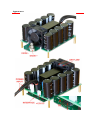
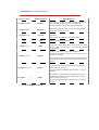
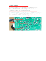
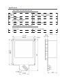
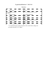
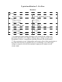
rev 1.05 / 2013 10 01
PDD-02 : Pulsed laser diode driver
User manual
Read carefully this document before start operations
Overview / Applications
PDD-02 is a pulsed diode driver with the possibility of high current
operations.
The maximal output current is 200A. The maximal output voltage is 6V. The
maximal output power is 100W-150W in dependence on the configuration.
Both short and long pulse widths are possible. In some cases CW operations
is also possible.
Since PDD-02 supposes a lot of modifications different with current, voltage,
pulse width, at the stage of inquiry we ask you to specify the parameters you
need:
1. maximal output current IMAX (up to 200A)
2. maximal compliance voltage VMAX (up to 6V)
3. maximal pulse width needed TMAX (up to CW)
4. maximal repetition rate needed FMAX (up to 10kHz)
Example: PDD-02-200A-2V-300us-100Hz
Cooling / coverage case
Module is supplied as a printed board sandwich with a preinstalled fan.
Appearance
Connections, signals, signal descriptions
POWER INPUT
Power input is organized with two wires thick enough to supply high
currents needed. Power input positive is marked with a piece of red shrink
tube.
Recommended power input voltage is 1V above the actual diode voltage
measured with the voltage meter. Higher input voltage is possible, but the
maximal output power is reduced.
+12V DC: 2 PIN MOLEX MINIFIT
Input type connector
Feeds interface circuits of the module
PIN (color)
DESCRIPTION
1 (red)
+12V DC positive
2 (blue)
+12V DC negative (return)
Alternatively, +12V DC voltage can be supplied to the board through the
corresponding pin of INTERFACE connector.
OUTPUT: 2x STUDS WITH M6 THREAD
Output type connector
Connects the driver to the laser diode
PIN (color)
DESCRIPTION
output positive
(red mark)
to laser diode anode
output negative
(no mark)
to laser diode cathode
INTERFACE: 10 PIN connector
PIN (type, color)
DESIGNATION
DESCRIPTION
1 (output, purple)
TMonitor
The voltage at this pin is a monitor signal proportional
to the measured value of module’s temperature.
Calibration table is provided by the manufacturer.
2 (input, blue)
IProgram
The voltage applied to this pin sets the output current.
0-10V are linear with 0-IMAX
3,4 (input, red)
+12V DC
Feeds the interface circuits. The voltage should be
stabilized.
The current consumption is less than 500mA.
5,6
GND
Return of all interface circuits
Pulse
Once the driver is enabled its output starts to follow the
input Pulse signal. While Pulse is logical “0” no output
occurs; when Pulse is logical “1” (5V) current is applied
to the output
Enable
Apply +5V DC to this pin to enable PDD-02.
While 0V are applied to this pin or pin is unconnected
module is disabled.
Once fault case has occurred module is blocked till you
eliminate fault cause, then disable module and enable it
again.
Fault 2*
If module is enabled and some trouble has occurred,
module automatically stops operations and sets Fault
status (Fault is set to “0”).
In case of normal operations Fault is set to “1” (5V at
the pin).
Fault 1*
If module is enabled and some trouble has occurred,
module automatically stops operations and sets Fault
status (Fault is set to “0”).
In case of normal operations Fault is set to “1” (5V at
the pin).
7 (input, white)
8 (input, green)
9 (output, orange)
10 (output, yellow)
* see also Faults section
ENABLE JUMPER:
Use ENABLE JUMPER instead of ENABLE signal of INTERFACE (pin 8).
Don’t use ENABLE JUMPER and ENABLE signal at the same time.
CURRENT JUMPER AND CURRENT TRIMPOT:
Use CURRENT JUMPER instead of IPROGRAM signal of INTERFACE (pin 2). Once
this jumper is installed use CURRENT TRIMPOT to set desired output current value.
Don’t use CURRENT JUMPER and IPROGRAM signal at the same time.
Operations
1.
2.
3.
4.
5.
6.
Connect laser diode to the module (OUTPUT sockets)
Disable module, set Pulse off, set IProgram signal to 0V
Feed both DC powers to the module
Set desired value of output current (IProgram signal)
Enable module
Use Pulse signal to On/Off output current
To power down PDD-02
1. Set Pulse to 0V, then Disable module
2. Remove power from the module
Faults and protections
Module sets Fault state in the following cases:
• short circuit – Fault 1 is set to “0”, red LED is lighted.
• open circuit – Fault 2 is set to “0”, yellow LED is lighted.
• overheating (temperature of the module exceeds 78+/–2 °C level) –
both Fault 1 and Fault 2 are set to “0”.
Once Fault has occurred you should eliminate the fault cause, then “reboot”
module (Disable module and Enable it again).
The module has also protections from too long pulses (> 110% of TMAX) and
from too frequent pulses (>110% of FMAX). These protections don’t cause
fault cases.
Specifications
ELECTRICAL SPECIFICATIONS
INPUTS
OUPUTS
ENVIRONMENTAL
Operation temperature
Storage temperature
Humidity
see datasheet of your modification
see datasheet of your modification
+10 … +40 °C
-20 … +60 °C
90%, non-condensing
MECHANICAL SPECIFICATIONS
Dimensions
Weight
167 x 112 x 60 mm
0.5 kg
TMonitor calibration table (typical)
t,C - Tmonitor,V
29.20 - 4.92
30.00 - 4.66
34.00 - 4.29
37.00 - 4.00
42.50 - 3.50
49.20 - 3.00
56.00 - 2.50
64.00 - 2.00
74.00 - 1.50
78.00 - 1.34 protection from overheating
Typical modification 1 : Nd:YAG
Datasheet
INPUTS
Power input
Interface feeding
OUTPUT
Output current
Output voltage
Pulse width
Pulse repetition rate
Rise/fall time
Current overshoot
Current ripple
Current regulation accuracy
4V-5V *
+12V DC stabilized, 0.5A max
40A-200A adjustable
up to 2V
40us – 300us
0Hz – 200Hz
about 20us (with proper cable)
< 5% of IMAX
< 1% of IMAX
< 1% of IMAX
* recommended input voltage depends on the actual diode voltage and
preferably should be 2.6V higher
Typical modification 2 : Er:Glass
Datasheet
INPUTS
Power input
Interface feeding
OUTPUT
Output current
Output voltage
Pulse width
Pulse repetition rate
Rise/fall time
Current overshoot
Current ripple
Current regulation accuracy
4V-5V *
+12V DC stabilized, 0.5A max
40A-200A **
up to 2V **
40us – 3ms **
0Hz – 200Hz **
about 20us (with proper cable)
< 5% of IMAX
< 1% of IMAX
< 1% of IMAX
* recommended input voltage depends on the actual diode voltage and
preferably should be 2.6V higher; different input voltage increases heat
dissipation in driver’s components and thus decreases the performance
** these parameters aren’t independent and cannot achieve their maximums at
the same time because of possible driver’s overheating; even if the input
voltage is properly selected, the maximal output power cannot exceed
120W-150W