1
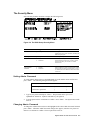
Digital HiNote VP 550, 575 Series
Service Guide
Part Number:
ER-PD1WF-SM. A01
Digital Equipment Corporation
Maynard, Massachusetts
March 1997
The information in this document is subject to change without notice and should not be construed as a commitment by
Digital Equipment Corporation.
Digital Equipment Corporation assumes no responsibility for any errors that might appear in this document.
The software described in this document is furnished under a license and may be used or copied only in accordance with the
terms of such license. No responsibility is assumed for the use or reliability of software or equipment that is not supplied by
Digital Equipment Corporation or its affiliated companies.
Restricted Rights: Use, duplication, or disclosure by the U.S. Government is subject to restrictions as set forth in
subparagraph (c) (1) (ii) of the Rights in Technical Data and Computer Software clause at DFARS 252.227-7013.
© Digital Equipment Corporation 1996. All Rights Reserved.
DEC, HiNote, ThinWire, and the Digital logo are trademarks of Digital Equipment Corporation.
ESS is a registered trademark of ESS Corp.
Pentium is a registered trademark of Intel Corporation.
Microsoft, MS-DOS and Windows are registered trademarks of Microsoft Corporation.
All other trademarks and registered trademarks are the property of their respective holders.
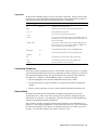
The FCC wants you to know...
This equipment has been tested and found to comply with the limits for a Class B digital
device, pursuant to Part 15 of the FCC rules. These limits are designed to provide reasonable
protection against harmful interference in a residential installation.
Any changes or modifications made to this equipment may void the user's authority to operate
this equipment.
This equipment generates, uses, and can radiate radio frequency energy and, if not installed
and used in accordance with the instructions, may cause harmful interference to radio
communications. However, there is no guarantee that interference will not occur in a
particular installation. If this equipment does cause harmful interference to radio or television
reception, which can be determined by turning the equipment off and on, the user is
encouraged to try to correct the interference by one or more of the following measures:
•
Reorient or relocate the receiving antenna.
•
Increase the separation between the equipment and receiver.
•
Connect the equipment into an outlet on a circuit different from that to which the receiver
is connected.
•
Consult the dealer or an experienced radio/TV technician for help.
All external cables connecting to this basic unit must be shielded. For cables connecting to
PCMCIA cards, see the option manual or installation instructions.
Table of Contents
1 Overview
System Overview................................ ................................ ................................ ................................ .... 1–1
CPU and Chip Set ................................ ................................ ................................ ........................... 1–1
Memory................................ ................................ ................................ ................................ ........... 1–1
BIOS................................ ................................ ................................ ................................ ............... 1–1
Video Controller Chip................................ ................................ ................................ ..................... 1–1
I/O Ports................................ ................................ ................................ ................................ .......... 1–1
Option Modules................................ ................................ ................................ ............................... 1–1
Components, Controls and Indicators................................ ................................ ................................ ..... 1–1
Front and Side Components (Panel Closed)................................ ................................ ..................... 1–1
Rear View ................................ ................................ ................................ ................................ ....... 1–1
Left and Side Components................................ ................................ ................................ ............... 1–1
Right Front View (Panel Open)................................ ................................ ................................ ....... 1–1
Controlling Power................................ ................................ ................................ ........................... 1–1
Battery Charge Gauge (in LCD Status Display)................................ ................................ ............... 1–1
LCD Status Display................................ ................................ ................................ ......................... 1–1
Keyboard Hot Keys................................ ................................ ................................ .......................... 1–1
Related Information ................................ ................................ ................................ ............................... 1–1
Documentation................................ ................................ ................................ ................................ 1–1
World Wide Web................................ ................................ ................................ ............................. 1–1
Bulletin Boards ................................ ................................ ................................ ............................... 1–1
2 System Restoration
Reinstalling/Installing Drivers ................................ ................................ ................................ ............... 2–1
Creating a Bootable Floppy................................ ................................ ................................ .................... 2–2
Using the Boot Floppy................................ ................................ ................................ ............................ 2–2
Re-installing the Operating System ................................ ................................ ................................ . 2–2
System Installation................................ ................................ ................................ .......................... 2–3
Complete System Restoration................................ ................................ ................................ .......... 2–3
Using the DIGITAL HiNote System CD................................ ................................ ................................ . 2–5
Preparing a New Hard Drive ................................ ................................ ................................ ........... 2–5
FDISK and Format Disk Utility................................ ................................ ................................ 2–5
PHDISKF Utility................................ ................................ ................................ ...................... 2–6
System Installation................................ ................................ ................................ .......................... 2–7
Complete System Restoration................................ ................................ ................................ .......... 2–8
v
3 System BIOS
BIOS Setup Program................................ ................................ ................................ .............................. 3–1
Navigating through the BIOS Setup Program................................ ................................ ......................... 3–2
Accessing the BIOS Setup Program................................ ................................ ................................ .3–2
Menu Bar ................................ ................................ ................................ ................................ .3–2
Item Specific Help................................ ................................ ................................ .................... 3–2
Legend Bar................................ ................................ ................................ ............................... 3–3
Launching Submenus................................ ................................ ................................ ...................... 3–3
General Help ................................ ................................ ................................ ................................ ...3–3
The Main Menu ................................ ................................ ................................ ................................ ..... 3–4
The Peripherals Menu ................................ ................................ ................................ ............................ 3–5
Integrated Peripherals (Peripherals submenu)................................ ................................ ......................... 3–6
The Security Menu................................ ................................ ................................ ................................ .3–7
Setting Admin. Password................................ ................................ ................................ ................. 3–7
Changing Admin. Password ................................ ................................ ................................ ............ 3–7
Deleting Admin. Password................................ ................................ ................................ .............. 3–8
Using Backup Password................................ ................................ ................................ ................... 3–8
The Power Menu................................ ................................ ................................ ................................ ....3–9
The Boot Menu................................ ................................ ................................ ................................ .... 3–10
The Exit Menu ................................ ................................ ................................ ................................ ..... 3–11
Modifying Flash BIOS................................ ................................ ................................ ......................... 3–12
Updating Flash BIOS ................................ ................................ ................................ .................... 3–12
Restoring the Flash BIOS................................ ................................ ................................ .............. 3–12
4 Troubleshooting
Troubleshooting Tips ................................ ................................ ................................ ............................. 4–1
System Start Failure ................................ ................................ ................................ ........................ 4–2
Power Supply Failure................................ ................................ ................................ ....................... 4–2
Boot-up Failure ................................ ................................ ................................ ............................... 4–3
Post Failure ................................ ................................ ................................ ................................ ..... 4–3
Password Failure ................................ ................................ ................................ ............................. 4–3
LCD Panel Failure................................ ................................ ................................ ........................... 4–3
CRT Failure ................................ ................................ ................................ ................................ ....4–4
Notebook Computer Keyboard Failure................................ ................................ ............................. 4–4
External Keyboard or PS/2 Mouse Failure................................ ................................ ....................... 4–5
HDD Failure................................ ................................ ................................ ................................ ....4–5
FDD Failure ................................ ................................ ................................ ................................ ....4–5
CD-ROM Failure................................ ................................ ................................ ............................. 4–6
Battery Failure................................ ................................ ................................ ................................ .4–6
Check Points and Error Messages................................ ................................ ................................ ........... 4–7
Phoenix BIOS Test Points................................ ................................ ................................ ............... 4–7
Warning Messages ................................ ................................ ................................ ........................ 4–10
5 FRU Replacement
Required Tools................................ ................................ ................................ ................................ ....... 5–1
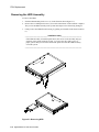
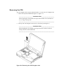
Removing the Battery................................ ................................ ................................ ............................. 5–2
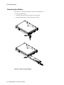
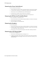
Removing the 12x CD/FDD Combination Module and Supplementary Battery................................ ...... 5–3
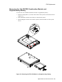
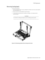
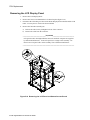
Removing the HDD Assembly................................ ................................ ................................ ................ 5–4
Removing the Keyboard................................ ................................ ................................ ......................... 5–5
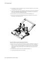
Removing the CPU................................ ................................ ................................ ................................ .5–7
Removing the LCD Assembly and Keyboard Deck................................ ................................ ................. 5–8
vi
Removing the Touch Pad................................ ................................ ................................ ..................... 5–13
Removing the DC-to-DC Converter Board................................ ................................ ........................... 5–13
Removing the System BIOS Chip................................ ................................ ................................ ......... 5–13
Removing the Audio Board................................ ................................ ................................ .................. 5–14
Removing the Motherboard................................ ................................ ................................ .................. 5–14
Removing the Power Switch Board................................ ................................ ................................ ....... 5–16
Removing the IR Receiver/Transmitter Board................................ ................................ ...................... 5–16
Removing the Speakers................................ ................................ ................................ ........................ 5–16
Removing the LCD Display Bezel................................ ................................ ................................ ........ 5–16
Removing the Status Display/Inverter Board................................ ................................ ........................ 5–17
Removing the LCD Display Panel................................ ................................ ................................ ........ 5–18
6 FRU List and Illustrated Parts Breakdown
FRU List ................................ ................................ ................................ ................................ ................ 6–1
LCD Display Assemblies, Panels, Boards, Housing................................ ................................ ......... 6–1
Motherboards, Daughterboards, Cache, IR, Power................................ ................................ ........... 6–2
Housings, Heatsinks, Miscellaneous Parts................................ ................................ ........................ 6–2
Trackpad ................................ ................................ ................................ ................................ ......... 6–2
Batteries................................ ................................ ................................ ................................ .......... 6–3
Keyboards................................ ................................ ................................ ................................ ....... 6–3
Disk Drives ................................ ................................ ................................ ................................ ..... 6–3
Option List................................ ................................ ................................ ................................ ............. 6–4
Illustrated Parts Breakdown................................ ................................ ................................ .................... 6–5
System IPBs................................ ................................ ................................ ................................ .... 6–5
System IPB List for TS31GA/GI................................ ................................ ............................... 6–9
System IPB List for TS31GN2................................ ................................ ................................ 6–10
System IPB List for TS31GL2................................ ................................ ................................ 6–11
Mechanical Parts List TS31G - All Units................................ ................................ ................ 6–13
LCD Assembly IPB for TS31GM/L................................ ................................ ............................... 6–15
LCD Assembly Listing for TS31GM/L................................ ................................ ................... 6–17
LCD Assembly IPB for TS31GA/I................................ ................................ ................................ . 6–18
LCD Assembly Listing for TS31GA/I................................ ................................ ..................... 6–20
A Specifications
Base Unit ................................ ................................ ................................ ................................ ............... A–1
Ports................................ ................................ ................................ ................................ ....................... A–2
Audio................................ ................................ ................................ ................................ ..................... A–2
LCD Display................................ ................................ ................................ ................................ .......... A–3
PCMCIA (PCI) ................................ ................................ ................................ ................................ ...... A–3
BIOS Support................................ ................................ ................................ ................................ ......... A–3
Battery, Status Display, Keyboard................................ ................................ ................................ .......... A–4
Physical................................ ................................ ................................ ................................ .................. A–4
B Device Mapping
Memory Map................................ ................................ ................................ ................................ ......... B–1
DMA Channel Assignments................................ ................................ ................................ ................... B–1
Notebook Computer Interrupt Levels................................ ................................ ................................ ...... B–2
I/O Address Map................................ ................................ ................................ ................................ .... B–3
vii
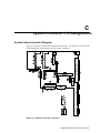
C System Connector Pin Assignments
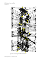
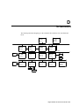
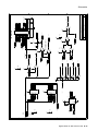
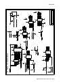
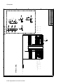
System Interconnection Diagram................................ ................................ ................................ ............ C–1
External KBD Connector – JP1................................ ................................ ................................ .............. C–2
Docking Connector – JP2A, JP2B, JP2C, JP2D, JP2E................................ ................................ ............ C–2
CRT Connector – JP3................................ ................................ ................................ ............................. C–5
Parallel Port Connector – JP4................................ ................................ ................................ ................. C–5
IR Connector – JP5 ................................ ................................ ................................ ................................ C–5
Serial Port(COM 1) – JP6................................ ................................ ................................ ....................... C–6
DC-to-DC Connector – JP7................................ ................................ ................................ .................... C–6
LCD Connector – JP8................................ ................................ ................................ ............................. C–6
PCMCIA Slot A – JP10................................ ................................ ................................ .......................... C–8
PCMCIA Slot B – JP11................................ ................................ ................................ .......................... C–9
DC-to-DC Connector – JP12 Conn2................................ ................................ ................................ ..... C–10
FDD Connector – JP13................................ ................................ ................................ ......................... C–11
Audio IN/OUT Connector – JP14................................ ................................ ................................ ......... C–11
IDE Connector – JP15................................ ................................ ................................ .......................... C–11
CD_ROM Drive Connector – JP18................................ ................................ ................................ ....... C–13
Track Pad Connector – JP2 ................................ ................................ ................................ .................. C–13
Audio Daughter Board Connector – JP20................................ ................................ ............................. C–14
MPEG Connector – JP21................................ ................................ ................................ ...................... C–14
Cache Connector – JP22................................ ................................ ................................ ....................... C–16
Cache Connector – JP23................................ ................................ ................................ ....................... C–17
Extend DRAM Connector – JP24................................ ................................ ................................ ......... C–18
Extend DRAM Connector – JP25................................ ................................ ................................ ......... C–19
Main Battery Connector – JP26................................ ................................ ................................ ............ C–20
CPU Daughter-Board Connector – JP17................................ ................................ ............................... C–20
CPU Daughter-Board Connector – JP16................................ ................................ ............................... C–22
Internal Keyboard Connector – J3................................ ................................ ................................ ........ C–24
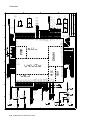
D Schematics
viii
Figures
Figure 1-1 Functional Block Diagram................................ ................................ ................................ ... 1–1
Figure 1-2 Right Front View (Panel Closed)................................ ................................ .......................... 1–1
Figure 1-3 Rear View................................ ................................ ................................ ............................ 1–1
Figure 1-4 Left Front View (Panel Closed)................................ ................................ ............................ 1–1
Figure 1-5 Right Front View (Panel open)................................ ................................ ............................. 1–1
Figure 3-1 The BIOS Setup Main Menu................................ ................................ ................................ 3–1
Figure 3-2 The BIOS Setup Peripherals Menu................................ ................................ ....................... 3–1
Figure 3-3 The BIOS Setup Integrated Peripherals Menu................................ ................................ ...... 3–1
Figure 3-4 The BIOS Setup Security Menu................................ ................................ ............................ 3–1
Figure 3-5 The BIOS Setup Power Menu................................ ................................ ............................... 3–1
Figure 3-6 The BIOS Setup Boot Menu................................ ................................ ................................ . 3–1
Figure 3-7 The BIOS Setup Exit Menu................................ ................................ ................................ .. 3–1
Figure 5-1 Removing the Battery................................ ................................ ................................ ........... 5–1
Figure 5-2 Removing the FDD /CD Module or Supplementary Battery................................ .................. 5–1
Figure 5-3 Removing HDD................................ ................................ ................................ ................... 5–1
Figure 5-4 Removing Keyboard Screw Caps and Screws................................ ................................ ....... 5–1
Figure 5-5 Removing Heatsink and Keyboard................................ ................................ ........................ 5–1
Figure 5-6 Removing the CPU Daughter Card................................ ................................ ....................... 5–1
Figure 5-7 Removing LCD Assembly End Caps and Hinge Screws................................ ....................... 5–1
Figure 5-8 Removing the Keyboard Deck (Part 1)................................ ................................ ................. 5–1
Figure 5-9 Removing the Keyboard Deck (Part 2)................................ ................................ ................. 5–1
Figure 5-10 Disconnecting the LCD Assembly Cable................................ ................................ ............ 5–1
Figure 5-11 Removing I/O Panel Screws................................ ................................ ............................... 5–1
Figure 5-12 Removing the Motherboard................................ ................................ ................................ 5–1
Figure 5-13 Removing the LCD Assembly Bezel................................ ................................ ................... 5–1
Figure 5-14 Removing the LCD Panel and Status/Inverter Board................................ .......................... 5–1
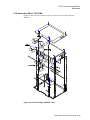
Figure 6-1 System Unit Assembly................................ ................................ ................................ .......... 6–1
Figure 6-2 System Unit IPB................................ ................................ ................................ ................... 6–1
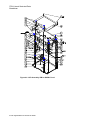
Figure 6-3 Detailed System Assembly TS31GN2/GL2................................ ................................ ........... 6–1
Figure 6-4 Detailed System IPB TS31GN2/GL2................................ ................................ .................... 6–1
Figure 6-5 LCD Assembly for GM/GL Panel................................ ................................ .......................... 6–1
Figure 6-6 LCD Assembly IPB for GM/GL Panel................................ ................................ .................. 6–1
Figure 6-7 LCD Assembly for GS/GO Panel................................ ................................ ........................... 6–1
Figure 6-8 LCD Assembly IPB for GA/GI Panel................................ ................................ .................... 6–1
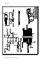
Figure C-1 System Connector Locations................................ ................................ ................................ C–1
ix
Preface
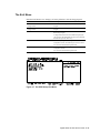
This guide describes how to test, troubleshoot, and remove and replace the Digital HiNote VP
500 series Models VP 550, 575 notebook computer Field Replaceable Units (FRUs).
Audience
This service guide is written specifically for service engineers.
Organization
This guide contains the following:
•
Chapter 1: Overview – This chapter introduces the Digital HiNote VP 500 series
notebook computers. It provides a system overview and describes the controls, indicators,
and hot keys.
•
Chapter 2: System Restoration – This chapter provides procedures for restoring the
operating system and system specific drivers.
•
Chapter 3: System BIOS – This chapter provides information related to the system BIOS
and its Setup program.
•
Chapter 4: Troubleshooting– This chapter provides a systematic method of isolating
problems with the Digital HiNote VP 500 series of notebook computers.
•
Chapter 5: FRU Replacement – This chapter provides detailed procedures for replacing
the Digital HiNote VP 500 series notebook computer Field Replaceable Units (FRUs).
•
Chapter 6: FRU List and Illustrated Parts Breakdown– This chapter provides a list of
the Field Replaceable Units (FRUs), parts breakdown and parts list for the Digital HiNote
VP 500 series Models VP 550, 575 notebook computer.
•
Appendix A: Specifications – This appendix lists the notebook computer’s specifications.
•
Appendix B: Device Mapping – This appendix contains tables listing the default settings
for of the notebook computer’s memory map, I/O address map, interrupt map, and DMA
map.
•
Appendix C: System Connector Pin Assignments– This appendix shows the location of
the connectors on the system motherboard and provides a listing of the pinouts for these
connectors.
•
Appendix D: Schematics – This appendix contains the schematic drawings for the
system.
Digital HiNote VP 500 Service Guide xi
1
Overview
This chapter introduces the Digital HiNote VP 500 series notebook computers. It provides a
system overview and describes the controls, indicators, and hot keys.
System Overview
The HiNote VP 500 series are high-performance portable computers designed for the mobile
professional.
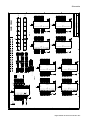
Figure 1-1 shows a functional block diagram of the notebook computer. The following
sections provide an overview of the different functions.
CPU and Chip Set
The HiNote VP 500 series notebook computers use theIntel P54CSLM 120/133 processors
and P55C 150/166/175 processors mounted on a daughter card.
The following chip set is used to implement the core functions of the system.
•
Intel Mobile Triton chip set provides system controller & PCI IDE controller functions
•
SMC669FR provides support for floppy disk controller (FDC), two serial ports (one serial
port and one FIR) and one parallel port
•
Intel 80C51SL provides the keyboard controller and scanner and the battery management
unit
•
Cirrus CL-PD6832 is used as the PCI PCMCIA controller
•
ESS ES1878 for the audio subsystem
Digital HiNote VP 500 Service Guide 1–1
Overview
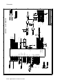
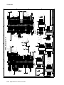
Figure 1-1 Functional Block Diagram
Memory
The system comes with 16MB of on-board DRAM for system memory and 256KB of L2
cache memory (on selected models).
System memory can be upgraded to a total of 24MB, 32MB, 48MB, and 80MB. The upgrade
is performed by installing two 4MB, 8MB, 16MB, or 32MB DIMM modules. Two identical
memory modules must be installed when adding additional memory.
BIOS
The system has a 256KB Flash ROM for system BIOS (Phoenix BIOS 4.04). The BIOS
provides support for the following:
•
Suspend to RAM/Disk
•
Full APM 1.2 supported
•
Password protection(System and HDD)
•
Auto-configured with replicator/docking/modules
•
Windows 95 ready with PnP
•
32KB ROM for 51SL keyboard controller
•
Gas-gauge for battery status information
•
Various hot-keys for system control
Video Controller Chip
Video support is provided by the Neo Magic NM2093 VGA Controller Chip. This chip
provides the following functions:
•
PCI Bus support
•
Simultaneous display supported
1–2 Digital HiNote VP 500 Service Guide
Overview
•
Integrated 128-bit wide, 7Mbits Display Memory – 1.1MB of Video RAM
•
Integrated programmable linear address feature accelerates GUI performance
•
Supports NON-interlaced CRT monitors with resolutions up to 1024 x 768/256 colors
•
Advanced power management features minimize power consumption during:
−
Normal operation
−
Standby mode
−
SUSPEND mode
−
VESA DPMS for monitor by 2093 (option)
•
Graphic accelerator for WINDOWS application
•
3.3V/5V panel Interface support
•
−
bit BLT Engine
−
Memory mapped I/O
−
Linear addressing
−
Color expansion
−
64x64 hardware cursor
−
64x64 or 128x128 hardware ICON
High resolution SVGA (800x600) panel
−
TFT displays support a maximum of 64K colors
−
DSTN displays support a maximum of 64K colors
I/O Ports
The system has the following I/O ports:
•
One 9 pin Serial port, 16550A compatible
•
One 25 pin Parallel port, EPP/ECP Capability
•
One 15 pin CRT port
•
6 pin external full keyboard/numeric key-pad / PS/2 mouse connector
•
One microphone in port & one speaker out port
•
240 pin docking connector that supports PS2 mouse port, AT-keyboard, 1S1P, CRT,
audio ports, MIDI port, and AC jack.
•
Built-in microphone
•
Built-in IRDA FIR transmitter-receiver
Digital HiNote VP 500 Service Guide 1–3
Overview
Option Modules
The following expansion modules can be installed in the system:
Secondary LiIon Battery
Components, Controls and Indicators
This section shows the locations and provides a description of the different components,
controls, and indicators on your Digital notebook computer.
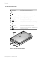
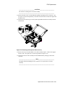
Front and Side Components(Panel Closed)
Component
Description
Removable Hard Drive
Easily removable and upgradable.
Lid Release
Slide the two latches located on either side of the notebook toward you to
open the LCD panel.
Main Battery Module
Removable batterymodule that can be replaced with a charged battery.
Expansion bay
Supports the 12X CD-ROM/FDD Combination moduleand optional
lithium-ion secondary batterymodule.
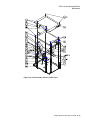
Figure 1-2 Right Front View (Panel Closed)
1–4 Digital HiNote VP 500 Service Guide
Overview
Rear View
Component
Description
Fast Infrared Interface
Allows wireless data transfer between the notebook and other IR
devices.
(Selected models only)
Serial (COM) Port
A serial device connects to this port.
Parallel LPT Port
A parallel device, such as a printer, connects to this port.
Reset Button
Using a pen or paper clip, press this button to reboot the system. All
unsaved data will be lost.
VGA Display Port
An external VGA or SVGA monitor connects to this port.
Minidock Port
This 240-pin port allows you to connect the notebook to the Minidock
Port
Replicator.
External Keyboard or PS/2
Mouse Port
An external keyboard or PS/2 mouse connects to this port.
Figure 1-3 Rear View
Digital HiNote VP 500 Service Guide 1–5
Overview
Left and Side Components
Component
Description
Speaker-out Port
External speakers or headphones connect to this port.
External Mic Port
An external microphone connects to the notebook.
PC Card Lower Socket Eject
Button
Ejects a PC Card Type II from the lower socket or to eject a Type III card.
PC Card Socket
Insert PC Card Type II or Type III cards into this socket.
PC Card Upper Socket Eject
Button
Ejects a PC Card Type II from the upper socket..
AC Power Port
The AC Adapter power cord connects to this port.
Security Lock Port
A Security Lock device, such as a Kensington Lock, connects to this port.
AC Power LED
Lights green when the notebook is operating on AC power.
Battery Charger LED
Lights amber when the battery is being charged. When the battery is fully
charged the amber LED turns off.
Figure 1-4 Left Front View (Panel Closed)
1–6 Digital HiNote VP 500 Service Guide
Overview
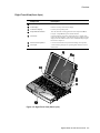
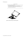
Right Front View(Panel Open)
Component
Description
Internal Microphone
Used to record music, voice and sound files.
LCD Display
DSTN or TFT Super VGA back-lit display.
LCD Status Display
Provides system operating status.
Suspend/Resume Button
Turns the notebook on and toggles between the suspend/resume
mode.
Press [fn + Suspend/Resume] to turn off the notebook.
Lid Switch
Close the notebook’s LCD lid to suspend the system. Open the lid to
resume the normal operation. The Lid Switch can be configured to CRT
display mode from within the Power menu of the BIOS Setup Program.
Please refer to Chapter 2.
Internal Stereo Speakers
Used to hear sound files and system sounds through stereo speakers.
Touch pad
A touch sensitive pointing device providing all the functions of a twobutton mouse.
Figure 1-5 Right Front View (Panel open)
Digital HiNote VP 500 Service Guide 1–7
Overview
Controlling Power
Unique to Digital notebook’s, the suspend/resumebutton not only enables you to take
advantage of the built-in power saving features but also turns the notebook on and off.
Action
How to...
On
Press the Suspend/Resume button to turn the system on.
Suspend
When the system is on, press this button to place your system in Suspend
mode.
Resume
Press the Suspend/Resume button to resume normal operation from the
Suspend mode.
Off
To completely shut off your notebook, press and hold [fn +
suspend/resume] button until a system beep sounds, indicating that the
system has been successfully turned off.
Suspend
Lid Switch
In its factory default mode, closing the LCD lid will also enter the
notebook into Suspend mode. Refer to Chapter 3, in the section labeled
Power Menufor instructions on how to configure the Lid Switch function.
Battery Charge Gauge(in LCD Status Display)
Icon
When Displayed, Indicates…
76% to 100% battery operating time remaining. When the lines within
this icon are rotating, it indicates that the battery is being charged. When
the rotating stops, the battery is fully charged.
51% to 75% battery operating time remaining.
26% to 50% battery operating time remaining.
Low battery to 25% battery operating time remaining. The system’s
warning beep will sound. Save your work, replace the low battery with a
fully charged one or use an AC power source to run the notebook. The [fn
+ F7] keys shut off the warning beep. It also mutes all audio.
System has ceased charging the battery. An abnormal condition exists
causing the core of the battery to reach its maximum temperature and
battery charging has been suspended..
1–8 Digital HiNote VP 500 Service Guide
Overview
LCD Status Display
Icon
When Displayed Indicates...
Embedded Numeric Keypad is enabled by the hot key combination. The
keyboard’s embedded keypad functions as a cursor control keypad. When
displayed in conjunction with the Num Lock icon, the embedded keypad
functions as a numeric keypad.
Scroll Lock is enabled by a hot key combination.
Num Lock is enabled by a hot key combination.
Caps Lock is enabled.
Hard Disk Drive/CD-ROM is being accessed by the system.
Floppy Disk Drive is being accessed by the system.
The external monitor (CRT) or Simul mode is enabled. If the icon is blinking,
the system is in Save to RAM mode.
Digital HiNote VP 500 Service Guide 1–9
Overview
Keyboard Hot Keys
Hot keys are activated by holding down the f[n] key (located in the lower left corner of the
keyboard) and pressing the desired function key.
[fn] +
Function
[fn + esc]
Places the computer in StandbyMode.
[fn+A]
Places the computer in Save to RAM Mode.
[fn+F]
All open data and system settings are Saved to Disk.
[fn + F1]
Decreases brightness level.
[fn + F2]
Increases brightness level.
[fn + F4]
Switches between the three display modes:
1.
LCD Display
2.
LCD Display and External Monitor
3.
External Monitor only
Each time you press this hot key combination the computer changes to the next
display mode.
[fn + F5]
Decreases the display contrast (DSTN screens only).
[fn + F6]
Increases the display contrast (DSTN screens only).
[fn + F7]
Enables or disables audio/speaker output including system beep indicating low
battery.
[fn + F8]
Toggles the keyboard’s embedded key pad on and off. When used by itself, it
functions as a cursor control keypad. Press [fn+F9] and then the [fn+F8] hot
key combination to use the notebook’s numeric embedded keypad.
[fn + F9]
Toggles Num Lock on and off. Used by itself, fn+F9 enables an external
keyboard numeric keypad.
[fn + F10]
Toggles Scroll Lock on and off. The Scroll Lock functions in certain
applications, leaving the cursor in its current position while moving the screen
in the direction of the arrow pressed.
[fn + home/pause]
Pauses the display output. Press a key to resume.
[fn + end/break]
If Break is enabled, pressing this hot key sends a system break.
[fn + PrScr/ SysReq]
Determined by application software.
[fn + ↑]
Increases the audio volume.
[fn + ↓]
Decreases the audio volume.
1–10 Digital HiNote VP 500 Service Guide
Overview
Related Information
Documentation
DIGITAL HiNote VP 550, VP 575 Series
User’s Guide
Digital HiNote VP 550, VP 575 Series Quick
Reference Card
Quick Setup Guide
AC Adapter Bulletin
DIGITAL HiNote System CD
English
ER-PD1WF-UA
French
ER-PD1WF-UP
Italian
ER-PD1WF-UI
German
ER-PD1WF-UG
Spanish
ER-PD1WF-US
Japanese
ER-PD1WF-UJ
Simple Chinese
ER-PD1WF-U2
English
ER-PD1WF-BA
French
ER-PD1WF-BP
Italian
ER-PD1WF-BI
German
ER-PD1WF-BG
Spanish
ER-PD1WF-BS
Japanese
ER-PD1WF-BJ
Simple Chinese
ER-PD1WF-B2
English, French,
Italian, German,
Spanish, Japanese
ER-PD1WF-IM
English, Dutch,
Danish, Swedish,
Norwegian, Finnish
ER-PD1WF-IX
English, Simple
Chinese
ER-PD1WF-I2
English, French,
Italian, German,
Spanish, Japanese
ER-PB1WF-DM
AG-R49UA-BE
World Wide Web
Information such as drivers, BIOS updates, and on-line documentation is available from
Digital’s World Wide Web Site.
The URL for the site is: HTTP://WWW.WINDOWS.DIGITAL.COM/
Bulletin Boards
Digital maintains a BBS for its customers. This BBS has information such as drivers, BIOS
updates, and on-line documentation. The BBS number is: (508)496-8800
Digital HiNote VP 500 Service Guide 1–11
2
System Restoration
This chapter provides information on how to restore the operating system and drivers on a
Digital HiNote VP 500 series notebook computer. It provides instructions on how to create a
bootable floppy for the system and how to restore the system using the bootable floppy or the
DIGITAL HiNote System CD.
____________________________ Caution __________________________
Do not compress the boot drive using compression utilities. It will cause the
notebook computer’s Save to File feature to not function properly.
______________________________________________________________
Reinstalling/Installing Drivers
Reinstalling Drivers – The procedures for reinstalling certain drivers over an existing
installation is different than installting the drivers on a clean installation. For information on
how to reinstall drivers, refer to the latest version of the DIGITAL HiNote System CD.
Installing Drivers – In order to restore the system back to its original Digital factory shipped
configuration, you must install the HiNote VP 500 Series audio, video, track pad and network
drivers (the need to install the network driver depends upon the individual requirements). If
you have installed WinNT, you will also want to install the EPM (Enhanced Power
Management) driver located in the Driver/WinNT directory. Please refer to Chapter 5 of the
User’s Guide in the section labeled Installing PC Cards in WinNT 4.0, for information on
EPM features. These drivers are located on the DIGITAL HiNote System CD. To install any
of these drivers, please refer to the following instructions:
1.
Boot to Windows.
2.
Insert the DIGITAL HiNote System CD into the CD-ROM drive.
3.
From the Taskbar, click on Start and then Run. In the Run command box type
X:\CDInstall (X represents the drive letter of the CD-ROM).
4.
At the Welcome screen, click on Next. Then at the Install screen, click on Driver
Installation Instructions.
5.
Select the driver(s) you wish to install. A readme.txt file will appear. Print the file(s).
These are the installation instructions to install the selected drivers(s).
Digital HiNote VP 500 Service Guide 2–1
System Restoration
Creating a Bootable Floppy
To create a bootable floppy, perform the following:
1.
Boot to Windows. Insert the DIGITAL HiNote System CD into the CD-ROM drive.
Click on Start and then Run. In the Run dialog box command line typeX:\CDInstall
(X: represents the drive letter of the CD-ROM).
2.
Click through the Welcome screens until the Install Menu appears.
3.
Click on the Utilities box and then click on Next.
4.
Click on Create Boot Floppy and click on Next. Click on Next again.
5.
Insert a 3½ inch 1.44 MB floppy into the floppy disk drive. Follow the on-screen
instructions. The utility (Sysboot.exe) will format the floppy, make the floppy bootable
and copy appropriate system files to the floppy. Before creating the boot floppy, ensure
that the floppy is NOT write protected. Any previous data on the diskette will be erased.
6.
After the bootable floppy has been created, ensure that it is write protected. Paste a label
onto the diskette and label it HiNote VP 500 Series Bootable Floppy.
Using the Boot Floppy
The hard drive in the system has been partitioned using the FDISK utility. The hard drive has
also been formatted. A "SAVETOFILE.BIN" file has been created for the system by using
PHDISKF. Without Save-to-File.bin, it will not be possible to take advantage of the system's
Save to Disk power management feature.
FDISK, format and PHDISKF are located on both the DIGITAL HiNote System CD and the
bootable floppy, which can be created from the DIGITAL HiNote System CD.
Re-installing the Operating System
To re-install the Windows Operating System on top of the current Operating System, perform
the following:
1.
Insert the bootable floppy into the floppy disk drive. Power on the system. A list of
choices appear.
______________________________ Note____________________________
To exit this menu and go to a DOS prompt, press 2. To re-enter this menu from a
DOS prompt, type AUTOEXEC and press the Enter key. AUTOEXEC must be
typed from the A: prompt.
_______________________________________________________________
2.
Insert the Microsoft Operating System CD into the CD-ROM drive.
3.
From the bootable floppy Main Menu, choose Option 3 (Re-install).
4.
Follow Microsoft's on-screen instructions.
5.
Remove the Microsoft Operating System CD and insert the Digital HiNote System CD.
Run CDInstall. Click on the Next buttons until the Main Install screen appears.
6.
Click on Enhancements and Updates, and then click on Next. Follow the on-screen
instructions. These enhancements update the Microsoft Operating system.
7.
After re-installing the Operating System you should re-install all drivers. Please refer to
the section on Reinstalling/Installing Drivers for information on installation procedures.
2–2 Digital HiNote VP 500 Service Guide
System Restoration
System Installation
To remove all files from the hard drive and re-install Windows Operating System but NOT
remove the hard drive partitions, please perform the following.
1.
Insert the bootable floppy into the floppy disk drive. Power on the system. A list of
choices appear.
_____________________________ Note____________________________
To exit this menu and go to a DOS prompt, press 2. To re-enter this menu from a
DOS prompt, type AUTOEXEC and press the Enter key. AUTOEXEC must be
typed from the A: prompt.
______________________________________________________________
2.
Choose Option 4. This Option will Format the hard disk’s drive C: and then create a
86016 KB Save-to-file.bin This file is created by the PHDISKF Utility and enables the
use of the notebook's Save to Disk feature.
3.
Insert the Microsoft Operating System CD into the CD-ROM drive.
4.
Choose Option 5 (Install OS) from the bootable floppy Main Menu. This will run
Microsoft's OEMSETUP program from the Microsoft Operating System CD.
OEMSETUP runs SCANDISK and then installs the OS.
5.
Remove the Microsoft Operating System CD and insert the Digital HiNote System CD.
Run CDInstall. Click on the Next buttons until the Main Install screen appears.
6.
Click on Enhancements and Updates, and then click on Next. Follow the on-screen
instructions. These enhancements update the Microsoft Operating system.
7.
After re-installing the Operating System you should re-install all drivers. Please refer to
the “Reinstalling/Installing Drivers” section of this chapter for information.
8.
Create a directory on the hard drive for the operating system installation files.
Windows 95: Create a directory on the hard drive under C:\Windows called Options and
then make a directory under that called Cabs. The new directory path is
C:\Windows\Options\Cabs. Copy the Win95 directory from the Microsoft CD onto the
hard drive’s C:\Windows\Options\Cabs directory.
Windows NT: After completing the installation of Windows NT, locate the directory on
the Microsoft O/S CD labeled, I386. Copy this directory to the drive where the operating
system is located, most likely drive C:\. The files in this directory are needed when
installing certain drivers such as network drivers.
Complete System Restoration
To perform a complete system restoration on a new hard drive or to remove all files and repartition the hard drive and then install a Microsoft Operating System, please perform the
following:
1.
Insert the bootable floppy into the floppy disk drive. Power on the system. A list of
choices appear.
Digital HiNote VP 500 Service Guide 2–3
System Restoration
______________________________ Note____________________________
To exit this menu and go to a DOS prompt, press 2. To re-enter this menu from a
DOS prompt, type AUTOEXEC and press the Enter key. AUTOEXEC must be
typed from the A: prompt.
_______________________________________________________________
2.
Choose Option 7 from the bootable floppy Main Menu. This will initialize the hard disk
using FDISK. Running FDISK will erase all data from the hard drive. During FDISK,
you will be prompted for much information.
When running FDISK, we strongly recommend that you do not enable large disk
support,(choose NO, when asked). If you choose [YES] you will not be able to install
WinNT or a WIN95 non-SR2 operating system at a later time. Also make sure you set the
Active Partition flag to make it bootable.
______________________ Note to Advanced User____________________
Although OEMSETUP does FDISK the hard drive, the utility is NOT designed to
run with hard drives 2.1 GB or larger. It will cause unexpected results. Use the
FDISK Option provided on the boot media.
_______________________________________________________________
3.
Choose Option 4. This Option will Format the disk and then create a 86016 KB Save-tofile.bin This file was created by the PHDISKF Utility and enables you to use the
notebook's Save to Disk feature.
4.
Insert the Microsoft Operating System CD into the CD-ROM drive.
5.
Choose Option 5 (Install OS) from the bootable floppy Main Menu. This will run
Microsoft's OEMSETUP program from the Microsoft Operating System CD.
OEMSETUP runs SCANDISK and then installs the OS.
6.
Remove the Microsoft Operating System CD and insert the Digital HiNote System CD.
Run CDInstall. Click on the Next buttons until the Main Install screen appears.
7.
Click on Enhancements and Updates, and then click on Next. Follow the on-screen
instructions. These enhancements update the Microsoft Operating system.
8.
After re-installing the Operating System you should re-install all drivers. Please refer to
the “Installing Drivers” section of this chapter for information.
9.
Create a directory on the hard drive for the operating system installation files.
Windows 95: Create a directory on the hard drive under C:\Windows called Options and
then make a directory under that called Cabs. The new directory path is
C:\Windows\Options\Cabs. Copy the Win95 directory from the Microsoft CD onto the
hard drive’s C:\Windows\Options\Cabs directory.
Windows NT: After completing the installation of Windows NT, locate the directory on
the Microsoft O/S CD labeled, I386. Copy this directory to the drive where the operating
system is located, most likely drive C:\. The files in this directory are needed when
installing certain drivers such as network drivers.
2–4 Digital HiNote VP 500 Service Guide
System Restoration
Using the DIGITAL HiNote System CD
This section describes the steps used to install a Microsoft Operating system and
drivers onto a new hard drive, or on an existing drive which needs restoration.
Preparing a New Hard Drive
PHDISKF and FDISK are the two utilities needed in order to prepare the hard disk for
general use. These utilities can be found on the DIGITAL HiNote System CD. The
FDISK utility formats the hard drive while the PHDISKF utility creates a DOS file on
the hard drive. This DOS file is necessary in order to take advantage of the notebook’s
Save to Disk power management feature.
FDISK and Format Disk Utility
The DIGITAL HiNote System CD is a bootable CD. It boots to the A:\ prompt. In the
following instructions we will be running the FDISK Utility on a 1.44GB hard drive.
1.
Insert the DIGITAL HiNote System CD into the CD-ROM tray. The CD should boot to
the A:\ prompt. At the A:\ type FDISK
the command line should read A:\FDISK.
Press <Enter>.
2.
This will execute the FDISK utility. When asked if you want to enable enlarged disk
support, choose [No]. If you choose [Yes], you will not be able to install WinNT or a
Win95 non-SR2 operating system.
3.
At the FDISK Main Menu, choose 1 to create a DOS partition or logical DOS drive. To
choose this option, type the number 1 and press <Enter>.
4.
Choose 1 again to create a primary DOS partition by typing 1 and pressing <Enter>.
5.
If you wish to make the whole hard drive one large partition, press <Enter> to accept the
default Yes. Continue to press the <esc.> key until you have exited FDISK and are at the
DOS prompt. Restart the system by pressing Ctrl+Alt+Del. Proceed to step 16. If you
wish to create multiple partitions on the hard drive, press the N key (signifying No) and
then press <Enter>. Proceed to step 6.
6.
FDISK will inform you of the approximate space available on the hard drive and prompts
you to enter the percent of disk space or the number of MB you wish to assign for the
primary partition. For the purpose of this example, we have chosen to assign drive C:
500MB.
7.
Type 500 and press <Enter>. FDISK displays the partition information. Press the <esc.>
key to continue.
8.
If you wish to make the primary partition C: bootable, type 2 and then press <Enter>.
You will be asked to enter the number of the partition you wish to make active (bootable).
Type 1, and press <Enter>. Press <esc.> to return to the FDISK Main Menu.
9.
If you wish to make more DOS partitions accessible by Win95, press 1, Create DOS
Partition or Logical DOS Drive (recommended) at the FDISK Main Menu. If you do not,
press <esc.> to exit the Main Menu and then press <esc.> again to exit FDISK. We have
chosen to Create a DOS Partition or Logical DOS Drive.
10. Press 2 to create an Extended DOS partition and then press <Enter>. FDISK will give
you the available hard disk space. On our 1.44 GB drive, the space remaining is 878MB.
11. If you wish to assign the remaining space as the Extended DOS partition, press <Enter>.
If you wish to customize the capacity, type in the amount in MB or percentage of the
available space (for ex, 50%) and press <Enter>. We will assign the remaining drive
space (878MB) to and Extended DOS partition.
Digital HiNote VP 500 Service Guide 2–5
System Restoration
12. After pressing <Enter>, press <esc.>. FDISK will inform you that there are no Logical
Drives assigned. Define the size you wish or press <Enter> to accept the default. If you
press <Enter> the entire (878MB) capacity will be assigned as drive D:.
13. Type the amount you wish drive D to be assigned. For our purposes we have chosen to
assign drive D 400MB, so we type 400. Press <Enter>. FDISK will display the
information for drive D: and inform you of the remaining capacity (478MB).
14. Press <Enter> to assign the remaining capacity to drive E:. All Extended DOS partitions
have been assigned to logical drives.
15. Press <esc.> to continue. Press <esc.> again to exit the FDISK Main Menu. You will be
informed that you need to reboot the system. Press <esc.> to exit FDISK. At the DOS
prompt, press Ctrl+Alt+Del to reboot the system.
16. The system will reboot to the CD-ROM. You must now format all partitioned segments
of the hard drive.
17. At the DOS prompt, type
Format C:/S/U and press <Enter>.
(There must be a space between the word “format” and “C”)
This will format the primary partition C, and copy all system files to the primary drive. If
you have created more than one partition you must format them as well. To format the D
drive for example, at the DOS prompt type:
Format D:/U and press <Enter>
(There must be a space between the word “format” and “D”.)
18. Continue until all partitions have been formatted. At the completion of Format Disk, you
will be returned to the DOS prompt. Refer to the following section on how to run the
PHDISKF Utility.
PHDISKF Utility
You will need to create a DOS File segment on the hard drive in order to take advantage of
the Save to Disk Power Management Feature. The DOS file can be created before or after you
install the operating system. Creating the DOS file after the installation of the operating
system will NOT erase any data from the hard drive. For the purpose of these instructions, we
have decided to first create the DOS file and then install the operating system. To use the
PHDISKF utility, please refer to the following instructions:
1.
Insert the DIGITAL HiNote System CD into the CD-ROM tray. The CD should boot to
the A:\ prompt. At the A:\, type PHDISKF /create 86016
There needs to be a space between the words “PHDISKF” and “/create”
and a space between “/create” and “86016”.
2.
Press <Enter>.
86016 represents the size of the DOS file to be create in KBytes. The equation for
determining the DOS file size is 1024 * (80MB + 4MB). 1024 is the number ofKBytes per
MegaByte. 80MB is the maximum amount of system memory and the additional 4MB is for
overhead.
Before you can load the Microsoft Operating System onto the hard drive, you must first load
the CD-ROM driver from the DIGITAL HiNote System CD to the hard drive. It is located in
the Driver directory.
2–6 Digital HiNote VP 500 Service Guide
System Restoration
System Installation
If you want to remove all files from the hard drive and re-install Windows Operating System
but NOT remove the hard drive partitions, please perform the following.
1.
Insert the Digital HiNote System CD into the CD-ROM drive and power on the system.
2.
Run format and then PHDISKF. Please refer to the appropriate sections of this chapter.
3.
Remove the Digital HiNote System CD and power off the notebook.
4.
Insert the bootable floppy into the floppy drive and turn on the system.
5.
At the list of options choose number 2 (exit to DOS). Insert the Microsoft CD into the
CD-ROM drive.
6.
From the DOS prompt, type the letter that represents the CD-ROM drive, then a colon
and a backslash. For example: D:\
7.
Enter the command to start the operating system installation:
Windows 95: D:\win95\setup
Windows NT: D:\winnt \b
D:\winnt
Use this command string if you do not want to create an
Emergency Backup Repair disk (recommended). You
must include a space between the “winnt” and the “\b”.
Use this command if you want to create an Emergency
Backup Repair Disk as a part of the installation.
8.
Press <Enter> and follow the instructions that appear on the screen to complete the
installation.
9.
Remove the Microsoft Operating System CD and insert the Digital HiNote System CD.
Run CDInstall. Click on the Next buttons until the Main Install screen appears.
10. Click on Enhancements and Updates, and then click on Next. Follow the on-screen
instructions. These enhancements update the Microsoft Operating system.
11. After re-installing the Operating System you should re-install all drivers. Please refer to
the “Installing Drivers” of this chapter for information.
12. Create a directory on the hard drive for the operating system installation files.
Windows 95: Create a directory on the hard drive under C:\Windows called Options and
then make a directory under that called Cabs. The new directory path is
C:\Windows\Options\Cabs. Copy the Win95 directory from the Microsoft CD onto the
hard drive’s C:\Windows\Options\Cabs directory.
Windows NT: After completing the installation of Windows NT, locate the directory on
the Microsoft O/S CD labeled, I386. Copy this directory to the drive where the operating
system is located, most likely drive C:\. The files in this directory are needed when
installing certain drivers such as network drivers.
Digital HiNote VP 500 Service Guide 2–7
System Restoration
Complete System Restoration
If you have purchased a new hard drive or you want to remove all files and re-partition the
hard drive and then install a Microsoft Operating System, please perform the following:
1.
Insert the Digital HiNote System CD into the CD-ROM drive and power on the system.
2.
Run FDISK, format the hard drive and then run PHDISKF. These instructions are
covered in detail in Appendix B of the User’s Guide.
3.
Remove the Digital HiNote System CD and power off the notebook.
4.
Insert the bootable floppy into the floppy drive and turn on the system.
5.
At the list of options choose number 2 (exit to DOS). Insert the Microsoft CD into the
CD-ROM drive.
6.
From the DOS prompt, type the letter that represents the CD-ROM drive, then a colon
and a backslash. For example: D:\
7.
Enter the command to start the operating system installation:
Windows 95: D:\win95\setup
Windows NT: D:\winnt \b
D:\winnt
Use this command string if you do not want to create an
Emergency Backup Repair disk (recommended). You
must include a space between the “winnt” and the “\b”.
Use this command if you want to create an Emergency
Backup Repair Disk as a part of the installation.
8.
Remove the Microsoft Operating System CD and insert the Digital HiNote System CD.
Run CDInstall. Click on the Next buttons until the Main Install screen appears.
9.
Click on Enhancements and Updates, and then click on Next. Follow the on-screen
instructions. These enhancements update the Microsoft Operating system.
10. After re-installing the Operating System you should re-install all drivers. Please refer to
the “Installing Drivers” section of this chapter for information.
11. Create a directory on the hard drive for the operating system installation files.
Windows 95: Create a directory on the hard drive under C:\Windows called Options and
then make a directory under that called Cabs. The new directory path is
C:\Windows\Options\Cabs. Copy the Win95 directory from the Microsoft CD onto the
hard drive’s C:\Windows\Options\Cabs directory.
Windows NT: After completing the installation of Windows NT, locate the directory on
the Microsoft O/S CD labeled, I386. Copy this directory to the drive where the operating
system is located, most likely drive C:\. The files in this directory are needed when
installing certain drivers such as network drivers.
2–8 Digital HiNote VP 500 Service Guide
3
System BIOS
This chapter provides information related to the system BIOS and its Setup program.
BIOS Setup Program
The BIOS (Basic Input and Output System) Setup Program is a menu driven utility that
enables you to make changes to the system configuration and tailor the operation of your
notebook to suit your individual work needs. It is a ROM-based (Read only Memory
)
configuration utility that displays the system’s configuration status and provides you with a
tool to set system parameters. These parameters are stored in non-volatile battery backed-up
CMOS RAM, which saves this information even when the power is turned off. CMOS chips
are extremely low power consuming. When the system is turned back on, the system is
configured with the values found in CMOS.
_____________________________ Note____________________________
The CMOS battery receives a charge when the system is being operated on AC
power. If the system is off for more than one year, the CMOS battery will drain
and the ROM data will be lost.
______________________________________________________________
By activating user friendly menus, you can configure such items as:
•
Hard drives, diskette drives and peripherals
•
Password protection from unauthorized use
•
Power Management Features
The settings made in the Setup program affect how the notebook performs. It is important to
try to understand all the Setup options and to make settings appropriate for the way you use
the notebook.
Digital HiNote VP 500 Service Guide 3–1
Navigating through the BIOS Setup Program
When turning on the notebook for the first time you may get a message prompting you to run
the BIOS Setup program. A warning message may appear on the screen if the hardware
configuration is changed or the Power On Self Test (POST) fails. This message will inform
you of any errors or invalid settings and prompt you to run Setup to correct the problem.
Even if you are not prompted by a message instructing you to use Setup, at some time in the
future you may want to change the configuration of your computer. For example, you may
want to make changes to the power management settings, or for security purposes, enable the
notebook’s password function. It will then be necessary to reconfigure your system using the
Setup program so that the computer can recognize these changes.
A few examples of why you may want to run the BIOS setup program follow.
•
You want to redefine the communication ports to prevent any conflicts.
•
You want to make changes to the Power Management configuration.
•
You want to change the password or make other changes to the security setup.
Accessing the BIOS Setup Program
To access the BIOS Setup program, press the F2 key when prompted during bootup. There
are three essential elements to the BIOS screens: Menu Bar, Item Specific Help Window and
Legend Bar.
Menu Bar
The top of the screen has a menu bar with the following selections :
Main
Changes to the basic system config
uration are made from within this menu.
Peripherals
Use this menu to enable and make changes to the system port addresses and modes.
Security
Sets System and Boot/Resume password.
Power
From within this menu, you will be able to configure and enable Power Management
features.
Boot
Allows you to specify the device the system will boot from and the boot device sequence.
Exit
Use this menu to save changes, set factory defaults and exit the Setup program.
Item Specific Help
Note that on the right side of each BIOS Setup screen, there is a section labeledItem Specific
Help. While moving through the Setup program, note that explanations for the currently
highlighted field appear in the Item Specific Help window.
3–2 Digital HiNote VP 500 Service Guide
Legend Bar
At the bottom of the BIOS Setup screen you will notice a legend bar. The keys in the legend
bar allow you to navigate through individual setup menus. The following table lists the keys
found in the legend bar with their corresponding alternates and functions.
Legend Key
Alternate Key
Function
F1
Alt + H
Displays the General Help window.
ESC
Exits the current menu and returns you to the previous screen.
← or →
Selects a different menu bar item.
↑ or ↓
Moves the cursor up and down between fields.
<Tab>
Cycles the cursor forward through the particular highlighted field. If
the field has only one value, the Tab key will move the selection cell
down to the next field.
<Shift + Tab>
Cycles the cursor backward through the particular highlighted field .
If the field has only one value, the [Tab + Shift] key comb
ination will
move the selection cell up to the prev
ious field.
-
Scrolls backwards through the values of the hig
hlighted field.
minus key
F5
+
plus key
F6
Scrolls forward through the values of the highlighted field.
F9
Sets the fields for the active menu to their default values.
F10
Sets the fields for the active menu to their prev
ious values.
<Enter>
Executes commands or selects a submenu.
Launching Submenus
Notice that a pointer symbol appears next to selected fields in the menu screens. For example,
open the Peripherals Menu and you will see a pointer that resembles a triangle on its side next
to the Integrated Peripherals field. This symbol indicates that a submenu can be launched
from this field. A submenu contains additional options. To launch a submenu:
1.
Move the highlighted cell to the desired Menu Bar item and press <Enter>.
2.
Use the legend keys to navigate around the screen and make the needed configuration
changes.
3.
When you finish, press the [esc] key to exit the submenu and return tothe main screen.
General Help
In addition to the Item Specific Help window, the BIOS setup program also provides a
General Help screen. This screen can be called up from any menu by simply pressing the
function key, F1 or the [Alt + H] combination. The General Help screen lists the legend keys
with their corresponding alternates and functions.
The scroll bar to the right of the help window indicates that there is more information to be
displayed. Use the PgUp and PgDn keys or the up and down arrow keys ↑( ↓)to scroll through
the entire help document. Press <Home> to display the first page, press <End> to go to the
last page. To exit the help window press <Enter> or the <Esc> key.
Digital HiNote VP 500 Service Guide 3–3
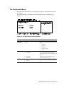
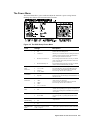
The Main Menu
The following settings are available in the Main Menu screen of the BIOS Setup Program.
Figure 3-1 The BIOS Setup Main Menu
Field
Settings
Description
Date
Enter current date: month, day, year
format
Sets the system to specified date.
Time
Enter current time: hour, minute, second
format
Sets the system to specified time.
Diskette A
Display only field
Indicates the presence and size of the FDD.
Hard Disk Drive
Display only field
Indicates the size of your notebook’s hard drive.
Total Memory
Display only field
Indicates the amount of total (RAM) memory.
Video Memory
Display only field
Indicates the amount of system video memory.
* Default value.
3–4 Digital HiNote VP 500 Service Guide
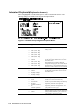
The Peripherals Menu
Notice the pointer icon next to the words Integrated Peripherals. This indicates the presence
of a submenu.
The following settings are available in the Peripherals Menu screen of the BIOS Setup
Program.
Figure 3-2 The BIOS Setup Peripherals Menu
Field
Settings
Description
Integrated
Peripherals
Submenu
Press Enter to set the following port addresses and
modes:
Video Mode
Touch Pad
•
Serial Port
•
Infrared Port
•
Parallel Port
•
Parallel Port Mode
•
Audio
Sets the Video mode
•
Simul Mode
Allows simultaneous viewing of externally
connected monitor (CRT) and the notebook’s LCD
display.
•
LCD Mode*
Allows viewing of the notebook’s LCD only.
•
CRT Mode
Allows viewing of the CRT only.
•
Enabled *
•
Disabled
Enables or disables the touch pad. Connecting a
mouse to the serial port will disable the Touch
Pad.
* Default value.
Digital HiNote VP 500 Service Guide 3–5
Integrated Peripherals(Peripherals submenu)
Move the highlighted cell to this field and press <Enter> to launch the submenu. The
following settings are available in the Integrated Peripherals Menu.
Figure 3-3 The BIOS Setup Integrated Peripherals Menu
Field
Settings
Description
Serial Port
•
Auto*
Enables, configures or disables the serial port
.
•
Disabled
•
COM 1 (3F8h - IRQ4)
Set the serial portto disable in order to increase the
battery run time.
•
COM 2 (2F8h - IRQ3)
•
COM 3 (3E8h - IRQ4)
•
COM 4 (2E8h - IRQ3)
•
Auto
Enables, configures or disables the infrared port
.
•
Disabled*
•
COM 1 (3F8h - IRQ4)
Set the infrared portto disable in order to increase
the battery run time.
•
COM 2 (2F8h - IRQ3)
•
COM 3 (3E8h - IRQ4)
•
COM 4 (2E8h - IRQ3)
When the FIR port is enabled two additional
configurable settings appear: Uart 2 Mode and Fast
IR DMA Channel. Choose the default settings for
these fields or refer to the IR device User’s manual.
•
Auto*
Enables, configures or disables the parallel port
.
•
Disabled
•
378h,IRQ7 or IRQ5
Set the parallel portto disable in order to increase
the battery run time.
•
278h,IRQ7 or IRQ5
•
3BCh,IRQ7 or IRQ5
•
Disabled
Disables the parallel port.
•
Normal
Parallel port is set for data-out mode only.
•
Bi-Directional *
Parallel port permits both data output and data input.
•
EPP Mode
(Extended Parallel Port)
Operates only with EPP aware peripherals.
•
ECP
(Extended Capabilities)
Operates only with ECP aware peripherals. See
your parallel device user’s guide.
•
Enables *
•
Disables
Enables, configures or disables the audio port. Some
DOS based software require editing the Audio chip’s
settings for DMA Channels, IRQ, etc. Please see
your application’s user guide for details.
Fast Infrared
Parallel Port
Parallel Mode
Audio
•
Default value.
3–6 Digital HiNote VP 500 Service Guide
The Security Menu
Select Security from the menu bar to display the following menu.
Figure 3-4 The BIOS Setup Security Menu
Field
Settings
Description
Admin. Password
[Press Enter]
Setting the Admin. Passwordwill limit
unauthorized access to the notebook, including the
BIOS Setup Program.
Backup Password
[Execute]
Backs up Admin. password to diskette.
Password on Boot
•
Enabled
•
Disabled *
When enabled, the system will require the Admin.
Password during system boot. If order to enable
Password on Boot, you must have an Admin.
Password set.
•
Enabled
•
Disabled *
Password on
Resume
When enabled, the system will required the Admin.
Password when resuming from suspend. In order
to enable Password on Resume, Password on Boot
must be set.
* Default value.
Setting Admin. Password
To set the Admin. Password, move the highlighted cell to the Admin. Password field and
press <Enter>. The following dialogue box will appear:
Set Admin. Password
Enter new password:
[
]
Confirm new password:
[
]
1.
Type in your password and press <Enter>. The password can be up to seven
alphanumeric characters. Symbols and other keys are ignored.
2.
Type the password in a second time to confirm. Press <Enter>. The System Passwordis
now set.
Changing Admin. Password
To change the Admin. Password, move the highlighted cell to the Admin. Password field and
press <Enter>. When the Admin. Password dialogue box appears, enter the new password.
Enter it a second time to confirm. The new password is now set.
Digital HiNote VP 500 Service Guide 3–7
Deleting Admin. Password
To delete a previously set Admin. Password and disable the password feature:
1.
Open the Admin. Password dialogue box.
2.
With the cursor in the Enter new password field, press <Enter>.
3.
The cursor will move to the Re-enter new password field. Press <Enter> again.
4.
When the Notice dialogue box appears notifying you that changes have been saved, press
<Enter> a third time. The password has been deleted.
Using Backup Password
It is highly recommended that you save backup your Admin. Password to a floppy diskette. To
backup the password:
1.
Insert a blank formatted floppy disk into the notebook’s floppy disk drive.
2.
From within the BIOS Setup Program’s Security Menu, move the highlighted cell to
Backup Password and press <Enter>.
3.
The password has successfully been backed up to the floppy. This is a hidden file.
4.
Remove the floppy from the drive, label it and then store it in a safe place. Please see
Chapter 7 for tips on floppy disk care.
To use the password backed up on floppy, please refer to the following:
1.
For the purpose of this illustration, we have assumed that you have set Password on Boot
to enable.
2.
Upon booting, the system will prompt you for the password. Insert the password floppy
into the notebook’s floppy disk drive.
3.
Type in the word “floppy” and press <Enter>. The system will continue with its boot.
4.
When prompted to by the system, press F2 to enter the BIOS Setup Program. Enter the
Security Menu and first delete the existing password by following the steps outlined in the
section labeled Deleting Admin. Password.
5.
After deleting the password, create a new one and back it up to a blank, formatted floppy
disk.
3–8 Digital HiNote VP 500 Service Guide
The Power Menu
The Power Menu allows you to enable and adjust the notebook’s power saving features.
Enabling these features will extend the battery run time.
Figure 3-5 The BIOS Setup Power Menu
Field
Settings
Description
Power Savings
•
•
Off
Sets the Power Management Mode.
Disables all Power Management
•
Customize *
Allows you to customize the Power Management fields
(Standby, Suspend, Suspend to Disk, Hard DiskTimeout) to suit your individual work needs.
•
Maximum Performance*
Power Management fields will be set with pre-defined
values to provide best system performance with some
power conservation.
•
Maximum Battery Life
Power Management fields will be set with pre-defined
values to ensure maximum battery run time.
Suspend-toDisk
Time-out
•
•
•
•
Disabled
1, 2, 3, 5 Min.
10 Min. *
15, 20, 30 Min.
Indicates the amount of time the system needs to be in
Save to RAM before entering Suspend
-to-Disk mode.
In order to make customized changes to this field,
Power Savings must be set to Customize.
Lid Switch
•
•
CRT
Suspend *
Sets action system performs when the notebook’s Lid
Switch is closed. If connecting an external monitor, set
this field to CRT.
Hard Disk
Time-Out
•
•
•
•
•
Disabled
1 Min.
2 Min. *
3 Min.
5, 10, 15, 20 Min.
Indicates the amount of time the hard diskneeds to be
inactive before it is turned off.
In order to make customized changes to this field,
Power Savings must be set to Customize.
AC Power
Save
•
•
On *
Off
When enabled all system power management is
enabled, when operating on AC power. If disabled, all
system power management is disabled when operating
on AC power.
Suspend Mode
•
•
Save to RAM*
Save to Disk
Selects Suspend mode the system will enter when
forced to suspend, i.e. pressing the suspend/resume
button.
Resume on
Modem Ring
•
•
OFF*
ON
If enabled, a modem ring will resume the system from
suspend mode.
Alarm Resume
•
•
OFF *
On
Enables or Disables Alarm Resume Time
Alarm Resume
Time
Enter time in a 24 hour format.
13:00 = 1:00 p.m.
Allows you to specify the time the system will resume.
* Default value.
Digital HiNote VP 500 Service Guide 3–9
The Boot Menu
From this menu you can choose where the system looks to boot from. You can also prioritize
the different boot devices.
Phoenix NoteBIOS Setup - Copyright Phoenix Technologies Ltd.
Main
Peripherals
Security
Power
Boot
Exit
Item Specific Help
1. Diskette Drive
Select item to relocate using
the Up and DOWN arrow keys.
Use the '+' and '-' keys to
move the highlighted boot
device up ('+') or down
('-') in the priority list.
2. Hard Drive
3. CD-ROM Drive
F1 Help
ESC Exit
Select Item
Select Menu
-/+ Change Values
Figure 3-6 The BIOS Setup Boot Menu
Field
Action
Boot Sequence
Description
This field allows you to prioritize which device
the system looks at to boot from. Move the
highlighted cell to the device you wish to select.
Use the + or - key to set its priority in the list.
•
Diskette First*
The system will attempt to boot from drive A.
If the drive is empty or a non-system disk is
present, the system will attempt to boot from the
next drive of priority.
•
Hard Disk Only
The system will boot from the hard disk
, drive
C only.
•
CD-ROM
The system will boot from the CD-ROM.
* Default value.
3–10 Digital HiNote VP 500 Service Guide
The Exit Menu
Enter the Exit Menu to save changes, set factory defaults or exit the Setup program.
Field
Action
Description
Save
Changes & Exit
<Enter>
Saves the current changes and exits the BIOS Setup
Program.
Discard
Changes & Exit
<Enter>
Discards the current changes and exits the BIOS Setup
Program.
Get Default Values
<Enter>
Loads the factory default values for each of the fields in the
BIOS Setup Program.
To keep default values and exit the BIOS Setup Program
,
you must move the highlighted cell to the Save Changes &
Exit field and press the <Enter> key.
Load Previous Values
<Enter>
Discards any changes made during the current BIOS
configuration session, and loads the prior session’s values.
You cannot exit the BIOS through this field.
Saves Changes
<Enter>
Saves the changes made during the current BIOS
configuration session.
You cannot exit the BIOS through this field.
Figure 3-7 The BIOS Setup Exit Menu
Digital HiNote VP 500 Service Guide 3–11
Modifying Flash BIOS
The Digital HiNote VP 500 Series notebook computer has a flash updatable system BIOS. As
improvements are made to the system BIOS they are made available from Digital’s Web site
or BBS.
Web Site: HTTP://WWW.WINDOWS.DIGITAL.COM
BBS: (508)496-8800
Updating Flash BIOS
The Flash BIOS update come as a self-extracting file that creates a bootable floppy disk. After
downloading the update procedure you restore the update image to floppy disk. This
procedure creates a bootable floppy with the PHLASH update program. The BIOS update is
provided with a set of instructions on how to use it.
Before running the BIOS update procedure set up the notebook computer as follows:
•
Connect the AC adapter. For the BIOS update to run the system has to be running from
its AC power source.
•
Remove any peripheral devices from the system:
•
−
PCMCIA devices
−
Port Replicator
Set the System BIOS to its factory default settings
To run the BIOS update:
1.
Insert the BIOS Update disk in the floppy drive.
2.
Cold boot the system.
a)
Press the [fn] + Suspend/Resume button to power off the system
b) Press the Suspend/Resume button to cold boot the system
3.
Follow the instructions provided by the update program.
Restoring the Flash BIOS
If for some reason the system BIOS becomes corrupted the BIOS chip located under the DCto-DC converter on the system motherboard will have to be replaced.
3–12 Digital HiNote VP 500 Service Guide
4
Troubleshooting
This chapter provides a systematic method of isolating problems with the Digital HiNote VP
500 Models VP 550, VP 575 series of notebook computers. It is assumed that you have a basic
understanding of DOS-based computer systems as well as a knowledge of standard
troubleshooting procedures. This manual is written under the assumption that the problems
are indeed related to the notebook computer itself. The improper usage of the system and
application software problems are excluded in this chapter.
The system BIOS power on self-tests (POST) are integral to the system and detect certain
errors with the system board. They use a series of beep codes to identify certain system board
problems.
The troubleshooting procedures when followed step by step, can help isolate system problems.
Troubleshooting Tips
In general, troubleshooting involves an organized system of approach to problem solving. Try
to isolate the problem and identify the defective device (hardware) or improper setting
(software). When you have a problem, you should do a thorough visual inspection of the
notebook computer.
•
If none of the indicators are lit and you cannot hear the HDD spinning, then the notebook
computer is probably not receiving power.
•
Make sure the power cord is plugged in, and the AC adapter is securely connected. The
LEDs on the AC adapter and the system should be on when connected to a working AC
source.
•
If you are using a power strip or surge protector, ensure that these devices are turned on.
Often problems are caused by improperly connected cables.
•
If you are using peripherals such as the mouse or keyboard, make sure they are properly
connected to their respective ports. Ensure that none of the connectors’ pins are bent or
broken.
•
Check all cables connected to the notebook computer. If any are cut, frayed, or damaged
in any way, replace them right away. Never use a damaged cable. A damaged cable is
not only a fire hazard, it may also cause a short circuit, resulting in irreparable damage to
the notebook computer.
•
Check all internal connections to ensure that they are secure. Often problems can occur
because a connection is loose or backwards.
Verify that all test equipment works before using it to test a malfunctioning component.
Digital HiNote VP 500 Service Guide 4–1
Troubleshooting
Verify that a component is the only malfunctioning part of the computer by replacing the
malfunctioning component with a properly functioning one, and then try to run the system.
For example, if you have tested an FDD in a test computer and found it to be bad, you should
also try a good FDD in the malfunctioning FDD’s computer to be sure that another component
(such as the FDD controller) is not bad as well.
As with assembly and disassembly, make sure you have adequate lighting, the right tools, and
a stable clean working environment.
The examples that follow provide useful tips and information that will help isolate and solve
some of the more common problems that may be encountered.
System Start Failure
When you turn on the computer, the system hangs before completing or starting the POST
(power on self test). Power supply failure, post failure, and boot-up failure can result in a
system start failure.
Power Supply Failure
Problem
Troubleshooting Procedure
You turn on the power switch and the following
conditions apply:
• There is no panel display
If you are operating the notebook computer using
the battery:
• The system could be in suspend. Press the
Suspend/Resume button.
•
There is no noise coming from the HDD
•
The power indicator light is off.
•
The battery connection is loose. Remove
and reinstall the battery.
•
The battery power is depleted. Plug in the
AC adapter, or replace the battery.
•
The battery needs to be reformed. Reform
the battery.
•
The system could be experiencing a hang.
Press the reset button (Figure 1-3).
If you are operating the notebook computer using
the AC adapter:
• Check that the AC adapter is plugged into
an operational power supply.
•
Check that the AC adapter is connected
securely to the notebook computer’s AC
adapter socket.
•
Check to see if the Power LED on the
computer is lit and the LED on the AC
adapter is lit. If not lit, then the AC adapter
is bad. Replace the AC adapter, and test the
notebook computer again.
•
Press the Suspend/Resume button
•
Press the system's "Reset Button"
located on the back of the unit between
the serial and parallel port connectors.
If the above items are functioning, then the
notebook computer’s internal power circuit is
probably damaged. Check the power circuit of
the notebook computer.
4–2 Digital HiNote VP 500 Service Guide
Troubleshooting
Boot-up Failure
Problem
Troubleshooting Procedure
You turn on the notebook computer and the
following conditions apply:
• The notebook computer’s power is on.
•
System in Suspend Mode. Press the
Suspend/Resume button.
•
System hung possibly hung after using
a screen saver. Press the Reset button
located on the back on the unit (Figure
1-3).
•
There is no screen display
Check the DRAM connections to be sure that
they are secure.
• Check the LCD connections.
•
Check the system board power circuit.
Post Failure
Problem
Troubleshooting Procedure
You turn on the computer and the following
happens:
• There is power to the system.
•
A POST failure usually indicates a
keyboard, memory, or HDD failure.
•
Check the error code or message against the
error codes and messages in this chapter.
•
The HDD seems to be spinning.
•
The screen is operational, and error codes
and messages are displayed.
Password Failure
Problem
Troubleshooting Procedure
You do not have the password or the password is
not known.
•
To clear the password, short Jumper 5 on
the motherboard.
LCD Panel Failure
Problem
Troubleshooting Procedure
You turn on the computer and one of the
following conditions apply:
• The system is working, but there is no LCD
panel display.
•
Make sure that the LCD cable is securely
connected to the Motherboard.
•
Make sure that the LCD cables are securely
connected to the inverter.
•
If the cables are securely connected and the
LCD still doesn’t work, replace the LCD
panel and test the system again.
•
If the display is garbled, verify the video
setup in the operating system’s Control
Panel Display application. If these are
correct, there is probably a VGA chip
failure. Replace the motherboard.
•
The system is working, but the LCD panel
display vertical or horizontal lines.
•
The backlight comes on, but there is no
display.
•
There is a display, but you have garbled
characters on the screen.
Digital HiNote VP 500 Service Guide 4–3
Troubleshooting
CRT Failure
Problem
Troubleshooting Procedure
The notebook computer has power, the notebook
computer’s LCD panel is working and one of the
following conditions apply:
• The notebook computer’s LCD panel is
working.
•
Make sure the CRT output is enabled.
•
Make sure that the CRT’s power is on anf
the power cables are securely connected.
•
Make sure that the CRT to notebook
computer cable connection is secure. Check
the CRT port on the notebook computer to
make sure the connection is secure, and that
there are no damaged pins or connectors.
•
Make sure the settings in the operating
system’s Control Panel Display application
are supported by the monitor.
•
If the CRT still doesn’t work, change to a
different CRT and try again.
•
If the color is bad, adjust the Monitor’s
color controls (if any).
•
There is no display on the CRT.
•
The color of the CRT is wrong.
•
There is a display, but the display is not
stable.
Notebook Computer Keyboard Failure
Problem
Troubleshooting Procedure
The notebook computer is fully powered-on.
However, when pressing any of the keys on the
keyboard, one of the following events occurs:
• Pressing on the key doesn’t have any effect.
•
If incorrect characters are displayed, check
the COUNTRY.SYS settings in the
operating system to see if an incorrect
language is being used by the system.
•
Incorrect characters are displayed on the
screen.
•
•
One stroke of a key produces too many
characters on the screen.
Make sure that the keyboard cable is
securely connected into the keyboard
connector.
•
Check the keyboard circuit.
•
Replace the keyboard and check again.
•
Replace the keyboard controller BIOS chip
located in the memory compartment on the
bottom of the system unit.
4–4 Digital HiNote VP 500 Service Guide
Troubleshooting
External Keyboard or PS/2 Mouse Failure
Problem
Troubleshooting Procedure
The notebook computer’s power is on, and the
keyboard is working. One of the following
conditions occur:
• Pressing keys on the external keyboard has
no effect.
•
Make sure that the external mouse or
keyboard’s connection to the notebook
computer’s PS/2 mini-DIN connector is
secure.
•
Make sure the mouse trackball and postion
sensors are clean and free of dust.
•
Replace the external mouse or keyboard and
try again.
•
If the system still doesn’t work, test the
mini-DIN keyboard circuit.
•
If incorrect characters are displayed, check
the COUNTRY.SYS settings in DOS to see
if an incorrect language is being used by the
system.
•
Pressing the key on the external keyboard
gives incorrect characters.
•
The mouse cursor on the screen doesn’t
move in conjunction with the external
mouse.
HDD Failure
Problem
Troubleshooting Procedure
When you try to access the HDD, one of the
following conditions occur:
• There is a message indicating that the HDD
doesn’t exist.
•
Check to make sure that the BIOS settings
are correct. Refer to Chapter 2 for BIOS
information.
•
Make sure that the HDD connection is
secure.
•
Install the HDD into another HiNote VP
550, VP 575notebook computer and test it.
•
If the HDD works in a test notebook
computer, the HDD controller on the
motherboard is probably bad. Test the
motherboard.
•
You can’t read from the HDD.
•
You can’t write to the HDD.
FDD Failure
Problem
Troubleshooting Procedure
The notebook computer’s power is on. The HDD
is functioning correctly. When you try to access
the FDD, one of the following conditions occurs:
• You can’t read from the FDD.
•
Make sure the CD-ROM/FDD module is
properly seated.
•
Switch to a different floppy disk and try
again. Make sure that the floppy isn’t write
protected.
•
Clean the FDD’s heads.
•
Change the CD-ROM/FDD module and test
again.
•
If the FDD is OK, than there is probably an
I/O chipset failure. Replace the main board.
•
You can’t write to the FDD.
•
You can’t hear the FDD motor spinning,
and the LED indicator light isn’t on.
Digital HiNote VP 500 Service Guide 4–5
Troubleshooting
CD-ROM Failure
Problem
Troubleshooting Procedure
The notebook computer’s power is on. The HDD
is functioning correctly. When you try to access
the CD-ROM, one of the following conditions
occurs:
• You can’t read from the CD-ROM.
•
Make sure the CD-ROM/FDD module is
properly seated.
•
Switch to a different CD-ROM disk and try
again.
•
•
Clean the CD-ROM’s lens.
•
Change the CD-ROM/FDD module and test
again.
•
If the CD-ROM is OK, than there is
probably an I/O chipset failure. Replace the
main board.
You can’t hear the CD-ROM motor
spinning, and the LED indicator light isn’t
on.
Battery Failure
Problem
Troubleshooting Procedure
The notebook computer’s AC power works.
When trying to use battery power, the notebook
computer doesn’t operate. However, when the
AC Adapter is connected, the battery charge
indicator flashes.
•
Make sure that the battery contacts are in
good condition.
•
Make sure that the battery terminals are
clean. If need be, clean the terminals with
contact cleaner.
•
Form the battery and try again.
•
Change the battery and try again.
•
Check to make sure that the AC power
supply (the AC adapter and AC adapter
cord) are OK. If they are not supplying the
correct voltage, it could damage the system.
4–6 Digital HiNote VP 500 Service Guide
Troubleshooting
Check Points and Error Messages
At the beginning of each POST routine, the BIOS outputs the test point error code to I/O
address 80h. Use this code during troubleshooting to establish at what point the system failed
and what routine was being performed.
If the BIOS detects a terminal error condition, it halts POST after:
•
Issuing a terminal error beep code and
•
Attempting to display the error code on upper left corner of the screen and on the port 80h
LED display
If the system hangs before the BIOS can process the error, the code displayed at port 80his
that of the last test performed. In this case, the screen does not display the error code.
Phoenix BIOS Test Points
The following is a list of the checkpoint codes written at the start of each test and the beep
codes issued for terminal errors:
Code
Beeps
POST Routine Description
02
Verify Real Mode
04
Get CPU type
06
Initialize system hardware
08
Initialize chipset registers with initial POST values
09
Set in POST flag
0A
Initialize CPU registers
0C
Initialize cache to initial POST values
0E
Initialize I/O
0F
Initialize the local bus IDE
10
Initialize Power Management
11
Load alternate registers with initial POST values
12
Jump to UserPatch0
14
16
Initialize keyboard controller
2-2-3
BIOS ROM checksum
18
8254 timer initialization
1A
8237 DMA controller initialization
1C
Reset Programmable Interrupt Controller
20
3-1-1
Test DRAM refresh
22
3-1-3
Test 8742 Keyboard Controller
24
Set ES segment register to 4 GB
28
Autosize DRAM
2A
Clear 512K base RAM
2C
3-4-1
Test 512K base address lines
2E
3-4-3
Test 512K base memory
30
Base 64K RAM Error
32
Test CPU bus-clock frequency
34
Test CMOS RAM
35
Initialize alternate chipset registers
37
Reinitialize the chipset
38
Shadow system BIOS ROM
Digital HiNote VP 500 Service Guide 4–7
Troubleshooting
Code
Beeps
POST Routine Description
39
Reinitialize the cache
3A
Autosize cache
3C
Configure advanced chipset registers
3D
Load alternate registers with CMOS values
40
Set Initial CPU speed
42
Initialize interrupt vectors
44
46
Initialize BIOS interrupts
2-1-2-3
Check ROM copyright notice
47
Initialize manager for PCI Option ROMs
48
Check video configuration against CMOS
49
Initialize PCI bus and devices
4A
Initialize all video adapters in system
4C
Shadow video BIOS ROM
4E
Display copyright notice
50
Display CPU type and speed
51
Initialize EISA board
52
Test keyboard
54
Set key click if enabled
56
Enable keyboard
58
2-2-3-1
Test for unexpected interrupts
5A
Display prompt "Press F2 to enter SETUP"
5C
Test RAM between 512 and 640k
60
Test extended memory
62
Test extended memory address lines
64
Jump to UserPatch1
66
Configure advanced cache registers
68
Enable external and CPU caches
6A
Display external cache size
6C
Display shadow message
6E
Display non-disposable segments
70
Display error messages
72
Check for configuration errors
74
Test real-time clock
76
Check for keyboard errors
7C
Set up hardware interrupt vectors
7E
Test coprocessor if present
80
Disable onboard I/O ports
82
Detect and install external RS232 ports
84
Detect and install external parallel ports
86
Re-initialize onboard I/O ports
88
Initialize BIOS Data Area
8A
Initialize Extended BIOS Data Area
8C
Initialize floppy controller
90
Initialize hard-disk controller
91
Initialize local-bus hard-disk controller
4–8 Digital HiNote VP 500 Service Guide
Troubleshooting
Code
Beeps
POST Routine Description
92
Jump to UserPatch2
94
Disable A20 address line
96
Clear huge ES segment register
98
Search for option ROMs
9A
Shadow option ROMs
9C
Set up Power Management
9E
Enable hardware interrupts
A0
Set time of day
A2
Check key lock
A4
Initialize typematic rate
A8
Erase F2 prompt
AA
Scan for F2 key stroke
AC
Enter SETUP
AE
Clear in-POST flag
B0
Check for errors
B2
POST done-prepare to boot operating system
B4
One beep
B6
Check password (optional)
B8
Clear global descriptor table
BC
Clear parity checkers
BE
Clear screen (optional)
BF
Check virus and backup reminders
C0
Try to boot with INT 19
DO
Interrupt handler error
D2
Unknown interrupt error
D4
Pending interrupt error
D6
Initialize option ROM error
D8
Shutdown error
DA
Extended Block Move
DC
Shutdown 10 error
The following Error Codes are related to the Boot Block in the Flash ROM:
E2
Initialize the chipset
E3
Initialize refresh counter
E4
Check for Forced Flash
E5
Check HW status of ROM
E6
BIOS ROM is OK
E7
Do a complete RAM test
E8
Do OEM initialization
E9
Initialize interrupt controller
EA
Read in the bootstrap code
EB
Initialize all vectors
EC
Boot the Flash program
ED
Initialize the boot device
EE
Boot code was read OK
Digital HiNote VP 500 Service Guide 4–9
Troubleshooting
If the BIOS detects error 2C, 2E, or 30 (base 64K RAM error), it displays an additional word
of information reflecting the bit or address line that failed. For example, if "2C 0002" is
displayed, address line 1 (represented by bit one) has failed. If "2E 1020" is displayed, then
data bits 12 and 5 have failed in the upper 16 bits.
The BIOS sends the same information to the port 80h LED display. The check point code is
followed by a delay, the high order byte, another delay, and then the low order byte of the
error. This is be repeated continuously.
Warning Messages
The following is an alphabetic list of error and status messages which the PhoenixBIOS can
generate and an explanation of each message. Many of the messages below refer to the built in
Setup program.
Message
Description
nnnn Cache SRAM Passed
nnnn is the amount of system cache in kilobytes
successfully tested.
Diskette drive A error
Drive A: is present but fails the BIOS POST diskette
tests. Check to see that the drive is defined with the
proper diskette type in Setup and that the diskette
drive is attached correctly.
Entering SETUP
Starting Setup program
Extended RAM Failed at offset: nnnn
Extended memory not working or not configured
properly.
nnnn Extended RAM Passed
nnnn is the amount of RAM in kilobytes successfully
tested.
Failing Bits: nnnn
The hex number nnnn is a map of the bits at the RAM
address (in System, Extended, or Shadow memory)
which failed the memory test. Each 1 (one) in the map
indicates a failed bit.
Fixed Disk 0 Failure or Fixed Disk 1
Failure or Fixed Disk Controller
Failure
Fixed disk is not working or not configured properly.
Check to see if fixed disk is attached properly. Run
Setup to ensure that the fixed-disk type is correctly
identified.
Incorrect Drive A type run SETUP
Type of floppy drive A: not correctly identified in
Setup.
Invalid NVRAM media type
Problem with NVRAM access.
Keyboard controller error
The keyboard controller failed test. You may have to
replace keyboard or controller.
Keyboard error
Keyboard not working.
Keyboard error nn
BIOS discovered a stuck key and displays the scan
code for the stuck key.
Keyboard locked Unlock key switch
Unlock the system to proceed.
Monitor type does not match CMOS
Run SETUP Monitor type not correctly identified in
Setup
Operating system not found
Operating system cannot be located on either drive A:
or drive C:. Enter Setup and see if fixed disk and
drive A: are properly identified.
Parity Check 1 nnnn Parity error
found in the system bus
BIOS attempts to locate the address but failed and
display it on the screen.
Parity Check 2 nnnn Parity error
found in the I/O bus
BIOS attempts to locate the address but failed and
display it on the screen.
4–10 Digital HiNote VP 500 Service Guide
Troubleshooting
Message
Description
Press <F1> to resume, <F2> to
Setup
Displayed after any recoverable error message: Press
<F1> to start the boot process or <F2> to enter Setup
and change any settings. <F2> Press <F2> to enter
SETUP Optional message displayed during POST.
Previous boot incomplete
Default configuration used
Previous POST did not complete
successfully
POST loads default values and offers to run Setup. If
the failure was caused by incorrect values and they
are not corrected, the next boot will likely fail.
Real time clock error
Real-time clock fails BIOS test. May require board
repair.
Shadow RAM Failed at offset: nnnn
Shadow RAM failed at offset nnnn of the 64k block at
which the error was detected.
nnnn Shadow RAM Passed
Where nnnn is the amount of shadow RAM in
kilobytes successfully tested.
System battery is dead - Replace and
run SETUP
The CMOS clock battery indicator shows the battery
is dead. Replace the battery and run Setup to
reconfigure the system.
System BIOS shadowed
System BIOS copied to shadow RAM.
System cache error
Cache disable RAM cache failed the BIOS test. BIOS
disabled the cache.
System CMOS checksum bad - run
SETUP
System CMOS has been corrupted or modified
incorrectly, perhaps by an application program that
changes data stored in CMOS. Run Setup and
reconfigure the system.
System RAM Failed at offset: nnnn
System RAM failed at offset nnnn of in the 64k block
at which the error was detected.
nnnn System RAM Passed
nnnn is the amount of system RAM in kilobytes
successfully tested.
System timer error
The timer test failed. Requires repair of system board.
UMB upper limit segment address:
nnnn
Displays the address of the upper limit of Upper
Memory Blocks, indicating released segments of the
BIOS which may be reclaimed by a virtual memory
manager.
Video BIOS shadowed
Video BIOS successfully copied to shadow RAM.
Digital HiNote VP 500 Service Guide 4–11
5
FRU Replacement
This chapter provides detailed procedures for replacing the Digital HiNote VP 500 series
notebook computer Field Replaceable Units (FRUs). Unless otherwise noted the replacement
procedures for the FRUs are the reverse of the removal procedures.
Required Tools
You will need the following tools to remove and replace the HiNote VP 500 series FRUs.:
•
#0 and #1 Phillips Head Screwdrivers
•
3/16 inch and 7/32 inch Nut Drivers
Digital HiNote VP 500 Service Guide 5–1
FRU Replacement
Removing the Battery
The battery is located on the right side of the system unit (Figure 5-1).
To remove the battery pack:
1.
Slide the battery lock/release clip to the release position.
2.
Pull the Battery Pack out of the system unit as shown.
Figure 5-1 Removing the Battery
5–2 Digital HiNote VP 500 Service Guide
FRU Replacement
Removing the 12x CD/FDD Combination Module and
Supplementary Battery
To remove the 12x CD/FDD Combination module or supplementary battery:
1.
Slide the locking button (1), located on the bottom of the system, in the direction shown
(Figure 5-2).
2.
Slide and hold the module release latch (2) in the direction shown.
3.
While holding the module release latch in position, slide the module out of the system
unit (3).
Figure 5-2 Removing the FDD /CD Module or Supplementary Battery
Digital HiNote VP 500 Service Guide 5–3
FRU Replacement
Removing the HDD Assembly
To remove the HDD:
1.
Slide the HDD module plastic cover (1) in the direction shown (Figure 5-3).
2.
Remove the two Philips head screws (2) located on the bottom of the notebook computer.
They secure the HDD assembly in the system unit and prevent it from being damaged.
3.
Gently remove the HDD from its housing, by pulling on its handle in the direction shown
(3).
_________________________ Installation Note_______________________
If the HDD assembly is installed upside down, the screws on the assembly may get
caught on some plastic inside the system. To remove the drive slide a piece of
paper (yellow sticky) between the unit and the plastic and slide the HDD assembly
out of the system.
_______________________________________________________________
Figure 5-3 Removing HDD
5–4 Digital HiNote VP 500 Service Guide
FRU Replacement
Removing the Keyboard
To remove the keyboard:
1.
Remove the keyboard screw caps by pulling them toward the front of the system and then
up as shown (Figure 5-4).
2.
Remove the two screws that hold the keyboard in place.
3.
Lift the keyboard up and rotate it toward the LCD display. The keyboard cable is
removed in step 5.
___________________________ CAUTION _________________________
Be careful not to damage the keyboard cable when lifting up the keyboard.
______________________________________________________________
Figure 5-4 Removing Keyboard Screw Caps and Screws
Digital HiNote VP 500 Service Guide 5–5
FRU Replacement
4.
Remove the heatsink (Figure 5-5).
a)
Remove the two screws that hold the heatsink in place.
b) Carefully lift the heatsink up and remove it from the system by sliding the keyboard
cable through the slot in the heatsink.
5.
Disconnect the keyboard cable (Figure 5-5).
a)
Release the cable latch by flipping it up. The latch is located across the back of the
connector.
b) Pull the cable out of the connector.
Figure 5-5 Removing Heatsink and Keyboard
5–6 Digital HiNote VP 500 Service Guide
Removing the CPU
The CPU daughter card is located under the heatsink. To remove the CPU daughter card:
1.
Remove the keyboard andheatsink (Figure 5-4, Figure 5-5).
________________________ Installation Note ______________________
When replacing the CPU heatsink, the torque of the heatsink screws should be set
to 2.3~3.0kg of force per cm².
______________________________________________________________
2.
Pull up on the CPU daughter card to remove if from the system (Figure 5-).
________________________ Installation Note ______________________
When installing the CPU daughter card, align each of the connectors with the
mating connector on the motherboard.
______________________________________________________________
Figure 5-6 Removing the CPU Daughter Card
FRU Replacement
Removing the LCD Assembly and Keyboard Deck
To remove the LCD Assembly:
1.
Remove the Battery (Figure 5-1).
2.
Remove the 12X CD/FDD Combination Module or Secondary Battery Figure
(
5-2).
3.
Remove the Keyboard and Heatsink (Figure 5-4, Figure 5-5).
4.
As a part of this procedure you will remove the Keyboard Deck. Before starting, close the
LCD Assembly, turn the system unit over, and remove the screw located at the top of
battery compartment (Figure 5-9).
5.
Open the LCD assembly and remove the left and right end caps by sliding them ¼ inch
toward the outside of the system unit and then up (Figure 5-7).
____________________________ CAUTION__________________________
The IR receiver/transmitter assembly is located under the right end cap. Care
should be taken when removing the right end cap.
_______________________________________________________________
6.
Remove the center cap and the LCD Assembly from the system unit as follows
(Figure 5-8):
a)
Release the front catches of the center cap by pressing in at the front base of the cap.
Be careful not to break the catches.
b) Release the rear catches of the center cap by pressing in at the rear base of the cap.
Be careful not to break the catches.
c)
Remove the Center cap.
______________________________ Note____________________________
•
There are two catches on the back of the center cap that hook on to nibs on the
Keyboard Deck. You have to press in on the bottom of the cover to get these
catches to release.
•
When replacing the center cap, insert the back first and then secure the front
catches.
_______________________________________________________________
7.
Remove the IR assembly. Gently twist the IR board clockwise to release it from one
locking tab. Twist the IR board counter clockwise to release it from the other locking tab.
8.
Remove the screw located under the right end cap. The IR receiver/transmitter must be
removed to access the screw.
9.
Remove the four hinge screws (Figure 5-7).
5–8 Digital HiNote VP 500 Service Guide
FRU Replacement
Figure 5-7 Removing LCD Assembly End Caps and Hinge Screws
Digital HiNote VP 500 Service Guide 5–9
FRU Replacement
10. Lift straight up on the LCD assembly to remove it from the system unit. The LCD cable
is still attached to the system unit.
11. Lay the panel on the work surface behind the system unit being careful not to damage the
cable. To prevent pulling on the LCD panel cable, you should lay the LCD panel on a
raised surface such as the CD-ROM/FDD module.
12. Remove the three screws across the back of the Keyboard Deck Figure
(
5-8).
13. Remove the screw that secures the Keyboard Deck to the motherboard. This screw is
located by the Touch Pad (Figure 5-8).
Figure 5-8 Removing the Keyboard Deck (Part 1)
14. Remove the two screws that secure the hard drive and remove the hard drive (Figure 5-8).
15. Make sure you have removed the screw from the underside of the battery compartment
(Figure 5-9). Remove the Keyboard Deck by releasing the catches as shown and lift the
Keyboard Deck off the system housing. The Touch Pad cable is still connected to the
motherboard.
16. Disconnect the Touch Pad cable from the motherboard (Figure 5-9).
17. Lay the Keyboard Deck on the LCD assembly.
5–10 Digital HiNote VP 500 Service Guide
FRU Replacement
___________________________ CAUTION _________________________
Be careful no to damage the LCD cable assembly.
______________________________________________________________
18. Remove the DC-to-DC Converter Board by pulling it straight up off its connectors. The
DC-to-DC converter board partially covers the LCD cable and is located to the right of the
PCMCIA slots.
19. Disconnect the cable that goes to the System Suspend/Resume button assembly from the
motherboard.
Figure 5-9 Removing the Keyboard Deck (Part 2)
18. Remove the two screws that hold the LCD cable assembly in place. Remove the support
bracket. Note: The right screw secures the ground wire (Figure 5-10).
19. Disconnect the LCD cable assembly from the Motherboard by lifting up on the cable
connector.
_____________________________ Note____________________________
The metal shield surrounding the cable connector is not a part of the LCD cable
assembly.
______________________________________________________________
Digital HiNote VP 500 Service Guide 5–11
FRU Replacement
________________________ Installation Notes______________________
1.
2.
Be sure to reconnect the ground wire.
When installing the end caps removed in step 6, make sure the nibs inside the
end caps slide into the appropriate catch on the Keyboard Deck.
3. The center cap has two catches that slide over nibs on the Keyboard Deck.
Install the back first and then the front.
_______________________________________________________________
Figure 5-10 Disconnecting the LCD Assembly Cable
5–12 Digital HiNote VP 500 Service Guide
FRU Replacement
Removing the Touch Pad
To remove the Touch Pad:
1.
Remove the LCD Assembly and the Keyboard Deck as described in this chapter.
2.
Remove the three screws that holds the Touch Pad in place.
3.
Remove the Touch Pad by disengaging the three metal catches that hold it in place. You
will have to work at carefully releasing these catches.
Removing the DC-to-DC Converter Board
To remove the DC-to-DC Converter board:
1.
Remove the LCD Assembly and the Keyboard Deck as described in this chapter.
2.
Locate the DC-to-DC Converter board. It is by the PCMCIA card slots at the back of the
system unit.
3.
Remove the board by pulling it straight up off its connectors.
Removing the System BIOS Chip
The system BIOS chip is located on the motherboard under the DC-to-DC Converter board.
To remove the system BIOS chip:
1.
Remove the LCD Assembly and the Keyboard Deck as described in this chapter.
2.
Locate the DC-to-DC Converter board. It is by the PCMCIA card slots at the back of the
system unit.
3.
Remove the board by pulling it straight up off its connectors.
4.
Using a chip puller, remove the BIOS chip.
___________________________ CAUTION _________________________
When installing the BIOS chip, make sure pin 1 is properly aligned. Failure to do
this will damage the chip, make the system not run, and possibly damage the
system.
______________________________________________________________
Digital HiNote VP 500 Service Guide 5–13
FRU Replacement
Removing the Audio Board
To remove the Audio Board:
1.
Remove the LCD Assembly and the Keyboard Deck as described in this chapter.
2.
Locate the Audio board. It is located over the HDD bay at the front of the system unit.
3.
Disconnect the audio cable that goes between the Audio board and the audio jacks.
a)
Release the cable lock by sliding the lock forward out of the connector.
b) Remove the cable from the connector.
______________________________ Note____________________________
The Audio jacks are soldered to the motherboard and cannot be removed.
_______________________________________________________________
4.
Remove the board by pulling it straight up off its connectors.
Removing the Motherboard
1.
Remove the Battery (Figure 5-1).
2.
Remove the 12X CD/FDD Combination Module or Secondary Battery (Figure 5-2).
3.
Remove the HDD Assembly (Figure 5-3).
4.
Remove the Keyboard and CPU daughter card (Figure 5-4, Figure 5-5).
5.
Remove the LCD Assembly and the Keyboard Deck as described in this chapter.
6.
Remove the Audio Board.
______________________________ Note____________________________
The Audio jacks are soldered to the motherboard and cannot be removed.
_______________________________________________________________
7.
Remove the eight nuts that secure the I/O ports and Docking connector to the back of the
system unit (Figure 5-11).
8.
Remove the five screws that secure the motherboard to the system housing Figure
(
5-12).
9.
–
Three screws are located across the back of the motherboard.
–
One screw is located in the PCMCIA card slot.
–
One screw is located under the Audio card.
Remove the HDD housing.
10. Remove the Motherboard from the system housing.
______________________________ Note____________________________
1.
For the Audio jacks to clear the side of the housing you will have to flex the
side of the housing.
2. For the FDD and CD connectors to clear their shields you have to flex the
shields out of the way.
_______________________________________________________________
5–14 Digital HiNote VP 500 Service Guide
FRU Replacement
Figure 5-11 Removing I/O Panel Screws
Figure 5-12 Removing the Motherboard
Digital HiNote VP 500 Service Guide 5–15
FRU Replacement
Removing the Power Switch Board
To remove the Power Switch board:
1.
Remove the Keyboard, LCD Assembly, and Keyboard Deck as described in this chapter.
2.
Locate the Power Switch board. It is attached to the underside of the Keyboard Deck.
3.
Remove the two screws that hold the Power Switch board in place.
4.
Disconnect the two speaker cables from the Power Switch board
5.
Disconnect the IR Receiver/Transmitter cable from the Power Switch board.
Removing the IR Receiver/Transmitter Board
To remove the IR Receiver/Transmitter board:
1.
Remove the Keyboard, LCD Assembly, and Keyboard Deck as described in this chapter.
2.
Remove the Power Switch board.
3.
Remove the IR Receiver/Transmitter board.
Removing the Speakers
To remove the Speakers:
1.
Remove the Keyboard, LCD Assembly, and Keyboard Deck as described in this chapter.
2.
Disconnect speaker cable(s) from the Power Switch board. You may want to remove the
Power Switch board to make this task easier.
3.
Remove the two screws that secureeach speaker to the bottom of the Keyboard Deck.
Removing the LCD Display Bezel
To remove the LCD display bezel:
1.
Remove the two rubber plugs and two screws F
( igure 5-13).
2.
Grasping an inside edge of the bezel pull it away from the center of the LCD assembly
until the plastic latches are disengaged. Do this on each side of the bezel until you can
remove the bezel.
5–16 Digital HiNote VP 500 Service Guide
FRU Replacement
Figure 5-13 Removing the LCD Assembly Bezel
Removing the Status Display/Inverter Board
1.
Remove the LCD Display Bezel.
2.
Remove the two screws that hold the Status Display/Inverter Board in place F
( igure 5-14).
3.
Remove the cable that goes to the LCD Panel (A).
4.
Remove the flat cable assembly (C).
a)
Release the cable lock by sliding the lock out of the connector.
b) Remove the cable from the connector.
Digital HiNote VP 500 Service Guide 5–17
FRU Replacement
Removing the LCD Display Panel
1.
Remove the LCD Display Bezel.
2.
Remove the four screws that hold the LCD Panel in place (Figure 5-14).
3.
Disconnect the cable that goes between the Status Display/Inverter Board and the LCD
Panel. You may have to remove the Inverter Board.
4.
Remove the flat cable assembly (B).
a)
Release the cable lock by slidingthe lock out of the connector.
b) Remove the cable from the connector.
____________________________ Important__________________________
LCD panels used in the Digital HiNote 500 series notebook computer are supplied
by different manufacturer’s. Each LCD panel uses a unique cable assembly. Do
Not mix an LCD panel with a cable assembly from a different manufacturer.
_______________________________________________________________
Figure 5-14 Removing the LCD Panel and Status/Inverter Board
5–18 Digital HiNote VP 500 Service Guide
6
FRU List and Illustrated Parts
Breakdown
This chapter provides a list of the Field Replaceable Units (FRUs) and a parts breakdown and
parts list for the Digital HiNote VP 500 series notebook computer.
FRU List
The following sections provide a list of FRUs and their part numbers for the Digital HiNote
VP 500 Series notebook computer.
LCD Display Assemblies, Panels, Boards, Housing
Digital FRU P/N
Compal P/N
Description
30-47967-01
2604211A01N
Assy, LCD Display 12.1", GM
30-48058-01
Assy, LCD Display 12.1", GL (LG)
30-48408-01
2604211A11L
Assy, LCD Display 12.1" DSTN (GN2-Sanyo JC53)
30-47974-01
2604221A01T
Assy, LCD Display Bezel, 12.1", GM
30-48409-01
2604221A11Q
Assy, LCD Display Bezel, 12.1", JC53
30-47978-01
2604231A01M
Assy, Housing Display Cover 12.1", GM
30-48059-01
2604231A02L
Assy, Housing Display Cover 12.1", LG
30-48422-01
2604231A11V
Assy, Housing Display Cover 12.1" (GN2-Sanyo
JC53)
30-47914-01
2604101A01Q
Assy, Inverter Board, 11.3/12.1"
30-47986-01
2604271A01L
LCD Panel, 12.1" IBM (3.3v ITSV50D)
30-48057-01
2604271A02L
LCD Panel, 12.1" LG
30-48419-01
2604271A03S
LCD Panel, 12.1" Sanyo (DSTN JC53)
30-47944-01
2604351A01Q
Assy, Cable, LCD/INV/MIC, 12.1" GM
30-48060-01
2694351A02N
Assy, Cable, LCD/INV/MIC, 12.1" LG
30-48643-01
2604351A04V
Assy, Cable, LCD/INV/MIC, 12.1" GL2
30-48644-01
2604351A03M
Assy, Cable, LCD/INV/MIC, 12.1" GN2
30-48420-01
DA331G2L204
Cable, LCD FPC for Sanyo,JC53 (w/Connector)
30-47915-01
2604181A01M
Bezel Screw Cap
Digital HiNote VP 500 Service Guide 6–1
FRU List and Illustrated Parts
Breakdown
Motherboards, Daughterboards, Cache, IR, Power
Digital FRU P/N
Compal P/N
Description
30-47913-01
2603971A01N
Assy, DC/DC Converter
30-48417-01
2606021A01R
Assy, PWR SW Board for 31G2
30-48412-01
2604241A12M
Assy, MLB 16MB, GN2/GL2 (-CPU/L2)
30-48022-01
2604291A01V
Assy, L2 Cache Board
30-48416-01
2606011A01M
Assy, IR Board for 31G2
30-47925-01
2604061A02S
CPU Daughter Card 120MHz/Intel
30-47926-01
2604251A01M
CPU Daughter Card 133MHz/Intel
30-48298-01
2608031A01L
CPU Daughter Card 150MHz MMX/Intel
30-48418-01
2604521A02V
CPU Daughter Card 166MHz MMX/Intel
30-48414-01
2603911A11N
Assy, Audio Board (with wave table)
30-48415-01
2603911A12M
Assy, Audio Board (w/o wave table)
30-48640-01
2604591A02U
Assy, MPEG Plate for 31G2
Housings, Heatsinks, Miscellaneous Parts
Digital FRU P/N
Compal P/N
Description
30-47912-01
2604051A01P
Assy, I/O Door
30-47917-01
2603871A01V
Screw Cover, Keyboard Deck, 11.3/12.1"
30-48410-01
2603891A11R
Assy, Deck, Keyboard for 31G2
30-48411-01
2604041A11S
Assy, Housing, Lower Main for 31G2
30-48413-01
2606001A11P
Assy, Heatsink for 31G2
30-48642-01
2603861A03M
Hinge, Cover set w/ IR lens for 31G2
30-47929-01
2604141A01N
Hinge, Support Bracket
30-47930-01
2604151A01T
Assy, Hinge (L/R)
74-51658-01
2604011A01R
Assy, PCMCIA Door
74-51669-01
2604021A01L
Tilt Leg (L/R)
30-47931-01
2604031A01Q
Assy, Memory Door
30-47932-01
2604171A01S
Feet, Rubber
30-47938-01
2604131A01U
Assy, Hook Knob
30-47933-01
2603881A01P
Assy, Speaker L/R
Digital FRU P/N
Compal P/N
Description
30-47934-01
2603931A01Q
Assy, Trackpad
30-47935-01
2603941A01V
Assy, Trackpad Button Board
Trackpad
6–2 Digital HiNote VP 500 Service Guide
FRU List and Illustrated Parts
Breakdown
Batteries
Digital FRU P/N
Compal P/N
Description
30-47939-01
2604191A01R
Battery, RTC, HiNote VP5h
30-48532-01
Spare Main Battery (ENiMH) - 3900mah
Keyboards
Digital FRU P/N
Compal P/N
Description
30-47960-01
2603811A07M
Keyboard, US/American, HiNote VP5h
30-47961-01
2603811A06N
Keyboard, Japanese, HiNote VP5h
30-47962-01
2603811A05Q
Keyboard, UK/British, HiNote VP5h
30-47963-01
2603811A04S
Keyboard, German, HiNote VP5h
30-47964-01
2603811A03U
Keyboard, French, HiNote VP5h
30-47965-01
2603811A02L
Keyboard, Italian, HiNote VP5h
30-47966-01
2603811A01M
Keyboard, Spanish, HiNote VP5h
30-47968-01
2604201A05M
Keyboard, Belgian, HiNote VP5h
30-47969-01
2604201A04N
Keyboard, Danish, HiNote VP5h
30-47970-01
2604201A03Q
Keyboard, Norwegian, HiNote VP5h
30-47971-01
2604201A02S
Keyboard, Swedish/Finnish, HiNote VP5h
30-47972-01
2604201A01U
Keyboard, Portuguese, HiNote VP5h
30-47973-01
2604201A06U
Keyboard, Swiss, HiNote VP5h
Digital FRU P/N
Compal P/N
Description
30-48296-01
2605821A01M
Combo Module (FDD/CD-ROM)
74-51657-01
2603781A01L
Door, HDD
30-47945-01
2603791A01Q
Assy, HDD Bracket/Cable (w/o HDD)
30-48641-01
2603921A01L
Holder, HDD (L) for 31G2
30-48647-01
2603801A04M
HDD, 1.44Gb, 2.5" x .5" H (Toshiba MK1401MAV) w/bracket assy
30-48648-01
2603801A03P
HDD, 2.1Gb, 2.5" x .5" H (Toshiba MK2103MAV) w/bracket assy
30-48649-01
2603801A06U
HDD, 2.1Gb, 2.5" x .5" H (IBM - DTNA-22160)
w/bracket assy
Disk Drives
Digital HiNote VP 500 Service Guide 6–3
FRU List and Illustrated Parts
Breakdown
Option List
Digital Opt P/N
Digital FRU P/N Compal P/N
Description
FR-PCP9E-BA
30-47949-01
Mini Dock w/o NIC, PR-1,
HiNote VP5h
FR-PCP9E-BB
30-47950-01
Mini Dock w/ NIC, PR-2,
HiNote VP5h
FR-PCP9H-BA
30-47922-01
Car Adapter, DC line cord,
HiNote VP5h
FR-PCP9H-BE
30-47951-01
Battery Charger, DC line cord,
HiNote VP5h
FR-PPC9H-BP
30-48533-01
Spare Main Battery (Li-Ion),
HiNote VP 500 II - 4050mah
FR-PCP9H-BN
30-48534-01
OPT Li-Ion Battery, HiNote
VP 500 II
FR-PCP9H-BW
30-47980-01
2603831A01M
Intl AC Adapter, w/o AC Cord,
HiNote VP5h
30-47941-01
2603821A01S
AC Adapter Module, Adapter
Only, HiNote VP5h
FR-PCP9H-BB
30-47981-01
Intl AC Adapter, US/Amer,
AC/DC Cord, HiNote VP5h
FR-PCP9H-BJ
30-47984-01
Intl AC Adapter, Japanese,
AC/DC Cord, HiNote VP5h
FR-PCP9H-BH
30-47985-01
Intl AC Adapter,
Australian/NZ, AC/DC Cord,
HiNote VP5h
FR-PCP9R-BA
30-47954-01
FR-PCP9R-BB
30-48535-01
FR-PCP9H-BK
30-48108-01
6–4 Digital HiNote VP 500 Service Guide
2604301A01M
Removable 1.44Gb HDD
Module, HiNote VP5h
Removable 2.1Gb HDD
Module, HiNote VP 500 II
2604621A01M
External FDD Cable, HiNote
VP5h
FRU List and Illustrated Parts
Breakdown
Illustrated Parts Breakdown
The following sections provide an illustrated parts breakdown of the Digital HiNote VP 500
series notebook computer. Each drawing has one or more tables with a parts description.
System IPBs
Figure 6-1 and Figure 6-3 show the system assembly. Figure 6-2 and Figure 6-4 show the
system assembly with part identifiers.
H
Figure 6-1 System Unit Assembly
Digital HiNote VP 500 Service Guide 6–5
FRU List and Illustrated Parts
Breakdown
527
261
H
269
528
270
271
Figure 6-2 System Unit IPB
6–6 Digital HiNote VP 500 Service Guide
FRU List and Illustrated Parts
Breakdown
H
N
L
K
N
L
J
K
P
M
P
H
F
J
M
Figure 6-3 Detailed System Assembly TS31GN2/GL2
Digital HiNote VP 500 Service Guide 6–7
FRU List and Illustrated Parts
Breakdown
509
373
2PCS
H
2PCS
531
2PCS
337
371
511
509
014
524
507
255
367
516
372
514
N
326
315
329
380
323
318
001
011
005
L
381
K
366
N
523
L
516
508
J
507
003
K
258
256
303
507
2PCS
365
P
383
2PCS
M
507
533
020
018
251
017
2PCS
007
019
317
254
386
512
P
507
H
513
F
322
3PCS
347
J
529
015
M
260
512
3PCS
016
252
311
308
4PCS
509
801
2PCS
800
6PCS
312
385
507
3PCS
384
374
362
379
324
389
390
320
2PCS
2PCS
2PCS
351
359
350
391
2PCS
526
348
392
382
388
387
316
394
2PCS
508
509
332
393
530
Figure 6-4 Detailed System IPB TS31GN2/GL2
6–8 Digital HiNote VP 500 Service Guide
2PCS
FRU List and Illustrated Parts
Breakdown
System IPB List for TS31GA/GI
Refer to Figure 6-2 and Figure 6-4.
Ref.
Compal No.
Description
54CB210YYKR
54CB310YYKV
001
CG0P4008003
SPEAKER 0.4W 8 OHM
KR-23-8AB (23mm)
2
2
003
DA3S31GL423
FLEXIBLE PCB TS31G
LF-194 REV2 T.PAD
1
1
005
DC020102507
HOUSING CONN. SET TS30G
SPEAKER-MB RIGHT
1
1
007
EC30G0BJ305
CPU HEAT SINK ASS'Y 30G0BJ
REV02
1
1
008
HGTS30P0604
80C51SL BIOS LABEL TS30P
SYSTEMSOFT 51SL LABEL
1
1
009
HGTS31A0016
SYSTEM BIOS LABEL TS31A
PHOENIX NOTEBIOS LABEL
1
1
* 011
PK090000707
TRACK PAD SYNAPTICS
TM1002SU D-GRY
1
1
014
DC020109609
HOUSING CONN. SET TS31G
SPK-L WIRESET
1
1
015
EE31G241006
VGA HEAT SINK 31G241
REV01
1
1
016
EE31G242002
MTSC HEAT SINK 31G242
REV01
1
1
251
4551810001V
PCBA, AUDIO BOARD LS-203
TS31G2
1
1
252
4351260001U
SMT ASSY, CACHE BD. LS-146 1
TS30G
1
254
4530980001U
PCBA,DC-DC CONVERTER PQ- 1
33C TS31G2
1
255
4552200001R
PCBA, F.I.R LS-207 TS31G2
1
1
256
4551790001M
PCBA, TRACK PAD LS-192
TS31G
1
1
258
4551830001U
PCBA, POWER SW BD. LS-201
TS31G2
1
1
260
4610640001S
CPCBA, W/FIRMWARE LA201
TS31G2
1
1
261
5103450021L
LCD ASSY TS31GA (WG013)
1
-
261
5103450031T
LCD ASSY TS31GI (WG013)
-
1
262
5103460001L
FDD MODULE TS31G (WG013)
1
1
266
X661090002T
MECHANICAL ASSY TS31G
(WG013)
1
1
267
X660790001M
SCREW SET REAL PANEL
SCREW
1
1
269
24CB21
K/B SET 30G
270
510283
HDD BRACKET ASSY TS30G
* 271
5103660003P
FDD/CD ROM 12X MODU
TS31G2 (WG013)
1
1
Digital HiNote VP 500 Service Guide 6–9
FRU List and Illustrated Parts
Breakdown
System IPB List for TS31GN2
Refer to Figure 6-2 and Figure 6-4.
54CB220YXXXX
54CB230YXXXX
Ref.
Compal No.
Description
YYKL
Y9KM
YYKQ
Y9KS
001
CG0P4008003
SPEAKER 0.4W 8 OHM
KR-23-8AB (23mm)
2
2
2
2
003
DA3S31GL423
FLEXIBLE PCB TS31G
LF-194 REV2 T.PAD
1
1
1
1
005
DC020102507
HOUSING CONN. SET TS30G
SPEAKER-MB RIGHT
1
1
1
1
007
EC30G221101
CPU HEAT SINK ASS'Y 30G221
REV01 (FOR 30G2)
1
1
1
1
008
HGTS30P0604
80C51SL BIOS LABEL TS30P
SYSTEMSOFT 51SL LABEL
1
1
1
1
009
HGTS31A0016
SYSTEM BIOS LABEL TS31A
PHOENIX NOTEBIOS LABEL
1
1
1
1
011
PK090000707
TRACK PAD SYNAPTICS
TM1002SU D-GRY
1
1
1
1
014
DC020109609
HOUSING CONN. SET TS31G SPK- 1
L WIRESET
1
1
1
015
EE31G241006
VGA HEAT SINK 31G241 REV01
1
1
1
1
016
EE31G242002
MTSC HEAT SINK 31G242 REV01
1
1
1
1
017
EL31G252004
CPU-HEATSINK MYLAR 31G252
REV01
1
1
1
1
018
FH31G246005
RUBBER FOR CPU-BOARD
31G246 REV01
2
2
2
2
019
FH31G247001
RUBBER WASHER 31G247 REV01
2
2
2
2
020
LC31G245003
SOCKET 31G245 REV01
2
2
2
2
251
4551810011S
PCBA, AUDIO BOARD LS-203
TS31G2(W/O W.T.)
1
1
1
1
252
4351260001U
SMT ASSY, CACHE BD. LS-146
TS30G
-
-
1
1
254
4530980001U
PCBA,DC-DC CONVERTER PQ33C TS31G2
1
1
1
1
255
4552200001R
PCBA, F.I.R LS-207 TS31G2
1
1
1
1
256
4551790001M
PCBA, TRACK PAD LS-192 TS31G
1
1
1
1
258
4551830001U
PCBA, POWER SW BD. LS-201
TS31G2
1
1
1
1
260
4610640041R
CPCBA, W/FIRMWARE LA201
TS31G2 (US) STN
1
-
1
-
260
4610640042P
CPCBA, W/FIRMWARE
LA-201 TS31G2 (UK) STN
-
1
-
1
261
5103450071S
LCD ASSY TS31GN2 (WG013)
1
1
1
1
6–10 Digital HiNote VP 500 Service Guide
FRU List and Illustrated Parts
Breakdown
54CB220YXXXX
54CB230YXXXX
Ref.
Compal No.
Description
YYKL
Y9KM
YYKQ
Y9KS
266
X661270001T
MECHANICAL ASSY TS31G2
(WG013)
1
1
1
1
267
X660790001M
SCREW SET REAL PANEL SCREW 1
1
1
1
269
24CB21
K/B SET 30G
270
510283
HDD BRACKET ASSY TS30G
271
5103660003P
FDD/CD ROM 12X MODU TS31G2
(WG013)
-
1
-
1
System IPB List for TS31GL2
Refer to Figure 6-2 and Figure 6-4.
54CB320YXXX
54CB330YXXX
Ref.
Compal No.
Description
YYKP
Y9KR
YWKU
YYKU
Y9KL
YWKN
001
CG0P4008003
SPEAKER 0.4W 8
OHM KR-23-8AB
(23mm)
2
2
2
2
2
2
003
DA3S31GL423
FLEXIBLE PCB TS31G 1
LF-194 REV2 T.PAD
1
1
1
1
1
005
DC020102507
HOUSING CONN. SET
TS30G SPEAKER-MB
RIGHT
1
1
1
1
1
1
007
EC30G221101
CPU HEAT SINK
ASS'Y 30G221 REV01
(FOR 30G2)
1
1
1
1
1
1
008
HGTS30P0604
80C51SL BIOS LABE
TS30P SYSTEMSOFT
51SL LABEL L
1
1
1
1
1
1
009
HGTS31A0016
SYSTEM BIOS LABEL
TS31A PHOENIX
NOTEBIOS LABEL
1
1
1
1
1
1
011
PK090000707
TRACK PAD
SYNAPTICS
TM1002SU D-GRY
1
1
1
1
1
1
014
DC020109609
HOUSING CONN. SET
TS31G SPK-L
WIRESET
1
1
1
1
1
1
015
EE31G241006
VGA HEAT SINK
31G241 REV01
1
1
1
1
1
1
016
EE31G242002
MTSC HEAT SINK
31G242 REV01
1
1
1
1
1
1
017
EL31G252004
CPU-HEATSINK
MYLAR 31G252
REV01
1
1
1
1
1
1
018
FH31G246005
RUBBER FOR CPUBOARD 31G246
REV01
2
2
2
2
2
2
019
FH31G247001
RUBBER WASHER
31G247 REV01
2
2
2
2
2
2
020
LC31G245003
SOCKET 31G245
REV01
2
2
2
2
2
2
Digital HiNote VP 500 Service Guide 6–11
FRU List and Illustrated Parts
Breakdown
54CB320YXXX
Ref.
Compal No.
Description
251
4551810011S
251
Y9KR
YWKU
YYKU
Y9KL
YWKN
PCBA, AUDIO BOARD 1
LS-203 TS31G2(W/O
W.T.)
1
1
-
-
-
4551810001V
PCBA, AUDIO BOARD LS-203 TS31G2
-
-
1
1
1
252
4351260001U
SMT ASSY, CACHE
BD. LS-146 TS30G
1
1
1
1
1
1
254
4530980001U
PCBA,DC-DC
CONVERTER PQ-33C
TS31G2
1
1
1
1
1
1
255
4552200001R
PCBA, F.I.R LS-207
TS31G2
1
1
1
1
1
1
256
4551790001M
PCBA, TRACK PAD
LS-192 TS31G
1
1
1
1
1
1
258
4551830001U
PCBA, POWER SW
BD. LS-201 TS31G2
1
1
1
1
1
1
260
4610640001S
CPCBA,
W/FIRMWARE LA201
TS31G2
1
-
-
1
-
-
260
4610640002Q
CPCBA,
W/FIRMWARE LA-201
TS31G2 (UK)
1
-
-
1
-
260
4610640003N
CPCBA,
W/FIRMWARE LA-201
TS31G2 (JP)
-
1
-
-
1
261
5103450061V
LCD ASSY TS31GL2
(WG013)
1
1
1
1
1
1
266
X661270001T
MECHANICAL ASSY
TS31G2 (WG013)
1
1
1
1
-
1
267
X660790001M
SCREW SET REAL
PANEL SCREW
1
1
1
1
1
1
269
24CB21
K/B SET 30G
270
510283
HDD BRACKET ASSY
TS30G
271
5103660003P
FDD/CD ROM 12X
MODU TS31G2
(WG013)
1
-
-
1
-
-
6–12 Digital HiNote VP 500 Service Guide
YYKP
54CB330YXXX
FRU List and Illustrated Parts
Breakdown
Mechanical Parts List TS31G - All Units
Refer to Figure 6-2 and Figure 6-4.
Ref.
Compal No.
Description
Qty
303
EC31G037001
TRACK PAD BRACKET31G037 REV01
1
308
EL30G08H102
I/O MYLAR 30G08H REV01
1
311
EC31G04R007
RELEASE MODULE 31G04R REV01
1
312
EC31G021008
I.O BRACKET 31G021 REV01
1
315
FC31G04B107
IR LENS 1 31G04B REV01
1
316
FC31G03G002
RAM COVER 31G03G REV01 WG013(DECK269)
1
317
EC31G03S105
HDD-HOLD L 1 31G03S REV01
1
318
FB31G041000
TRACK PAD KONB(D) 31G041 REV01 (WG015)(DECK271)
1
320
FA31G215000
LOGIC-LOWER 31G215 REV01 (WG013)
1
322
EL30G0CW104
HDD PVC MYLAR 30G0CW REV01
1
323
FB31G043002
POWER KONB 31G043 REV01 (WG015)(DECK271)
1
324
FC31G04J009
I/O DOOR HINGE 31G04J REV01 WG013(DECK269)
2
326
FA31G214003
LOGIC-UPPER 31G214 REV01 (WG014)
1
329
FB31G042006
TRACK PAD KONB(H) 31G042 REV01 (WG015)(DECK271)
1
332
FC31G249009
MPEG PLATE 1 31G249 REV01 (FOR EMI)
1
337
FH30G0BQ108
NON-WOVEN (SPEAKER) 30G0BQ REV01
2
347
EL30G0C7108
DOCKING MYLAR 30G0C7 REV01
1
348
LC1031D0607
AUDIO GASKET 5X5X5
2
350
FB31G04L006
LOCK KNOB 31G04L REV01 WG013(DECK269)
1
351
FB31G04M002
MODULE LOCK KNOB 31G04M REV01 WG013(DECK269)
1
359
FH30G0C8105
I/O SPONGE 30G0C8 REV01
2
362
FC31G03P009
I/O DOOR ASS'Y 31G03P REV01 (WG013)(DEC269)
1
366
EL30G08N109
TRACK PAD MYLAR 30G08N REV01
1
367
FH31G04X002
SPONG (IR) 31G04X REV01
1
371
FC31G036102
HI-CEN-CAP (FOR EMI) 31G036 REV01
1
372
FC31G034002
HINGE COVER(R) 31G034 REV01 (WG013)(DECK269
1
373
FC31G044008
SCREW COVER 31G044 REV01 (WG014)(DECK270)
2
374
EC31G038008
LOCK BRACKET 31G038 REV01 (KENSINGITON)
1
380
FH31G04U008
TRACKPAD SPONG 1 31G04U REV01
2
381
FH31G04T005
TRACKPAD SPONG 2 31G04T REV01
2
382
EC31G03Q102
SUPPORT-BRACKET 1 31G03Q1 REV01
1
383
MAB10025304
SCREW TPB-2.0X4FP-ZK
2
384
FH31G04Z000
IO-DOOR RUBBER 31G04Z REV01
1
385
FC31G082007
PCMCIA-DOOR ASS'Y 31G047 REV01
1
386
EC31G04S003
FPC-CONN-HOLD 31G04S REV01
1
387
EL31G08Y007
MYLAR FOR BATTERY 30G08Y REV01
1
Digital HiNote VP 500 Service Guide 6–13
FRU List and Illustrated Parts
Breakdown
Ref.
Compal No.
Description
Qty
388
EL30G24H100
MODULE COVER MYLAR 30G24H REV01
1
389
EC30G24K102
GROUND FINGER 30G24K REV01 (FOR CD ROM)
1
390
FH31G24A007
SPONG(6X5X3.0) 31G24A REV01
1
391
FH31G24B004
SPONG(6X5X2.0) 31G24B REV01
1
392
EL31G24C007
PRESSURE PANEL 31G24C REV01
1
393
EL31G24D001
TEFLON (56X45) 31G24D REV01
1
394
FH30G24J108
EMI SHIELDING GASKET 30G24J REV01
1
Qty
Ref.
Compal No.
Description
001
002
507
MAAA0001406
SCREW M3.0X0.5+5FP-MC
11
11
508
MAAA0002305
SCREW M2X0.4+3FP-ZK
3
3
509
MAAA0003409
SCREW M3X0.5+3FP-MC
8
8
511
MAAA0303208
SCREW M3X0.5+5FP-MC
1
1
512
MAA10023402
SCREW M2X0.4+3F-ZK
5
5
513
MAAA0003301
SCREW M3X0.5+5FP-ZK
1
1
* 514
MAA10005307
SCREW M2X0.4+8F-ZK
1
1
516
MAB10024006
TAPING SCREW TPB-2.0+5F-NI
2
2
523
FC31G08G000
SPEAKER HOLD(R) 31G08G REV01
1
1
524
FC31G08H003
SPEAKER HOLD(L) 31G08H REV01
1
1
* 526
MAAA0006301
SCREW M2X0.4+10FP-ZK
4
2
527
MAA20098201
SCREW TPB-M3X14.5P-NI
4
4
528
MAA10026401
SCREW M2.6X0.45+6F-ZK
2
2
529
MACA0308409
SCREW M3X0.5+8FP-NI
1
1
530
MAAA0006203
SCREW M3X0.5+4F-ZK
1
1
531
FH31G08N005
SPEAKER HOLD SPONGE 31G08N REV01
2
2
* 533
MAAA0006408
SCREW (NL) M2X0.4+10FP-ZK (NL)
-
2
* 515
6–14 Digital HiNote VP 500 Service Guide
FRU List and Illustrated Parts
Breakdown
LCD Assembly IPB for TS31GM/L
Figure 6-5 shows the LCD assembly. Figure 6-6 shows the LCD assembly with part
identifiers.
Figure 6-5 LCD Assembly for GM/GL Panel
Digital HiNote VP 500 Service Guide 6–15
FRU List and Illustrated Parts
Breakdown
Figure 6-6 LCD Assembly IPB for GM/GL Panel
6–16 Digital HiNote VP 500 Service Guide
FRU List and Illustrated Parts
Breakdown
LCD Assembly Listing for TS31GM/L
Refer to Figure 6-6.
Compal
Ref.
Number
Description
* 001
AC600003806
LCD MODULE ITSV50D 12.1" (IBM)
* 001
LCD MODULE (LG)
002
EC31G039101
HINGE SUPPORT 31G039 REV01 (BRACKET)
003
EC31G04C003
MIC HOLDER 31G04C REV01
004
EC31G04F004
HINGE(R) 31G04E REV01
005
EC31G04E001
HINGE(L) 31G04F REV01
006
EF31G04Q008
SPRING 31G04Q REV01
007
EFTS387E007
HIMELON (SPEAKER) TS387E REV01
008
FA31G012001
LCD-BEZEL(12.1") 31G012 REV01
009
FA31G011005
LCD-COVER 31G011 REV01 (WG013)(DECK269)
009
FA31G011307
LCD-COVER 31G011 REV01 (IBM 12.1)
010
FB31G045005
HOOK KNOB(R) 31G045 REV01 (WG013)(DECK269)
011
FB31G046001
HOOK KNOB(L) 31G046 REV01 (WG013)(DECK269)
012
FC31G04A002
LED LENS 31G04A REV01
013
FC31G04G008
FPC HOLDER(L) 31G04G REV01
014
FC31G04H001
FPC HOLDER (R) 31G04H REV01
015
FH31D049103
RUBBER PAD 31D049 REV01
017
LC31G04I005
FPC HOLDER SCREW 31G04I REV01 (NUT)
018
MAAA0001406
SCREW M3.0X0.5+5FP-MC
019
MACA0000404
SCREW M3X0.5+5FP-MC
020
MAAA0005304
SCREW M3X0.5+8FP-MC(NL)
021
251
FLEXIBLE PCB
4530950001Q
PCBA, INVERTER PQ-33B TS31G
Digital HiNote VP 500 Service Guide 6–17
FRU List and Illustrated Parts
Breakdown
LCD Assembly IPB for TS31GA/I
Figure 6-7 shows the LCD assembly. Figure 6-8 shows the LCD assembly with part
identifiers.
Figure 6-7 LCD Assembly for GS/GO Panel
6–18 Digital HiNote VP 500 Service Guide
FRU List and Illustrated Parts
Breakdown
Figure 6-8 LCD Assembly IPB for GA/GI Panel
Digital HiNote VP 500 Service Guide 6–19
FRU List and Illustrated Parts
Breakdown
LCD Assembly Listing for TS31GA/I
Refer to Figure 6-7.
Compal
Ref.
Number
Description
001
AC600004306
LCD MODULE DSTN JC35 (SANYO)
002
EC31G039101
HINGE SUPPORT 31G039 REV01 (BRACKET)
003
EC31G04C003
MIC HOLDER 31G04C REV01
004
EC31G04F004
HINGE(R) 31G04E REV01
005
EC31G04E001
HINGE(L) 31G04F REV01
006
EF31G04Q008
SPRING 31G04Q REV01
007
EFTS387E007
HIMELON (SPEAKER) TS387E REV01
008
FA31G012001
LCD-BEZEL(12.1") 31G012 REV01
009
FA31G011005
LCD-COVER 31G011 REV01 (WG013)(DECK269)
010
FB31G045005
HOOK KNOB(R) 31G045 REV01 (WG013)(DECK269)
011
FB31G046001
HOOK KNOB(L) 31G046 REV01 (WG013)(DECK269)
012
FC31G04A002
LED LENS 31G04A REV01
013
FC31G04G008
FPC HOLDER(L) 31G04G REV01
014
FC31G04H001
FPC HOLDER (R) 31G04H REV01
015
FH31D049103
RUBBER PAD 31D049 REV01
017
LC31G04I005
FPC HOLDER SCREW 31G04I REV01 (NUT)
018
MAAA0001406
SCREW M3.0X0.5+5FP-MC
019
MACA0000404
SCREW M3X0.5+5FP-MC
020
MAAA0005304
SCREW M3X0.5+8FP-MC(NL)
021
DA331G2L107
FLEXIBLE PCB
251
4530950001Q
PCBA, INVERTER PQ-33B TS31G
6–20 Digital HiNote VP 500 Service Guide
A
Specifications
Base Unit
Model
Feature
VSS5120
1.08GB drive,
16MB RAM,
12.1” SVGA
DSTN
VSS5133
1.08GB drive,
16MB RAM,
12.1” SVGA
DSTN
VTS5150
1.44GB drive,
16MB RAM,
12.1” SVGA TFT
VTS5166
2.1GB drive,
16MB RAM,
12.1” SVGA TFT
CPU
P54 CSLM Pentium
(120 MHz to 10
MHz supported
P54 CSLM Pentium
(120 MHz to 10
MHz supported
P54 CSLM Pentium
(120 MHz to 10
MHz supported
P55 Pentium MMX
(133 MHz to 166
MHz supported
CPU Speed
120 MHz
133 MHz
150 MHz
166 MHz
Cache L1
16KB Internal
16KB Internal
16KB Internal
32KB Internal
Cache L2
N/A
256KB on daughter
card
256KB on daughter
card
256KB on daughter
card
Architecture
(Mobile Triton)
PCI
PCI
PCI
PCI
Standard RAM
16MB (EDO)
16MB (EDO)
16MB (EDO)
16MB (EDO)
Maximum RAM
80MB
80MB
80MB
80MB
RAM Upgrade
Dual DIMM
Dual DIMM
Dual DIMM
Dual DIMM
PC95A Compliant
Yes
Yes
Yes
Yes
Diskette and CDROM Combo drive
3.5" floppy
12X CD-ROM
250ms access
1500Kbps transfer
rate
3.5" floppy
12X CD-ROM
250ms access
1500Kbps transfer
rate
3.5" floppy
12X CD-ROM
250ms access
1500Kbps transfer
rate
3.5" floppy
12X CD-ROM
250ms access
1500Kbps transfer
rate
Diskette supports
Japanese Mode
Yes
Yes
Yes
Yes
HDD Size
2.5"
12.5mm height
2.5"
12.5mm height
2.5"
12.5mm height
2.5"
12.5mm height
HDD (user
upgradable)
1.08GB
1.08GB
1.44GB
2.1GB
Integrated Pointing
Device
Trackpad
Trackpad
Trackpad
Trackpad
Digital HiNote VP 500 Service Guide A–1
Specifications
Ports
Model
Port
VSS5120
1.08GB drive,
16MB RAM,
12.1” SVGA
DSTN
VSS5133
1.08GB drive,
16MB RAM,
12.1” SVGA
DSTN
VTS5150
1.44GB drive,
16MB RAM,
12.1” SVGA TFT
VTS5166
2.1GB drive,
16MB RAM,
12.1” SVGA TFT
Keyboard/Mouse
Port
PS/2
PS/2
PS/2
PS/2
External Video
Interface
SVGA
SVGA
SVGA
SVGA
External Video,
Maximum
Resolution
1024x768
256 Colors
1024x768
256 Colors
1024x768
256 Colors
1024x768
256 Colors
External Video,
Refresh in
simultaneous mode
60 Hz
60 Hz
60 Hz
60 Hz
Serial Port
Yes
Yes
Yes
Yes
Parallel Port
ECP/EPP
ECP/EPP
ECP/EPP
ECP/EPP
Serial IR link
Fast IR
Fast IR
Fast IR
Fast IR
Microphone Jack
Yes
Yes
Yes
Yes
Audio
Model
Feature
VSS5120
1.08GB drive,
16MB RAM,
12.1” SVGA
DSTN
VSS5133
1.08GB drive,
16MB RAM,
12.1” SVGA
DSTN
VTS5150
1.44GB drive,
16MB RAM,
12.1” SVGA TFT
VTS5166
2.1GB drive,
16MB RAM,
12.1” SVGA TFT
Audio
16-bit Stereo
16-bit Stereo
16-bit Stereo
16-bit Stereo
Audio Controller
ESS 1878
ESS 1878
ESS 1878
ESS 1878
Audio
Compatibility
WSS and
SoundBlaster
with OPL3
Compatibility
WSS and
SoundBlaster
with OPL3
Compatibility
WSS and
SoundBlaster
with OPL3
Compatibility
Wave table, WSS
and SoundBlaster
with OPL3
Compatibility
Audio Volume
Control
Hot Key
Hot Key
Hot Key
Hot Key
Built-in
Microphone
Yes
Yes
Yes
Yes
Built-in Stereo
Speakers
Yes
Yes
Yes
Yes
A–2 Digital HiNote VP 500 Service Guide
Specifications
LCD Display
Model
Feature
VSS5120
1.08GB drive,
16MB RAM,
12.1” SVGA
DSTN
VSS5133
1.08GB drive,
16MB RAM,
12.1” SVGA
DSTN
VTS5150
1.44GB drive,
16MB RAM,
12.1” SVGA TFT
VTS5166
2.1GB drive,
16MB RAM,
12.1” SVGA TFT
Display Type
12.1" SVGA DSTN
Color
12.1" SVGA DSTN
Color
12.1" SVGA
TFT Color
12.1" SVGA
TFT Color
Video Processor
NM2093
NM2093
NM2093
NM2093
Video Accelerator
BitBLT Hardware
BitBLT Hardware
BitBLT Hardware
BitBLT Hardware
Video RAM
1.1MB
1.1MB
1.1MB
1.1MB
Graphic Resolution
800x600
800x600
800x600
800x600
Colors
64,000
64,000
64,000
64,000
Zoom Video
Yes
Yes
Yes
Yes
PCMCIA (PCI)
Model
Feature
VSS5120
1.08GB drive,
16MB RAM,
12.1” SVGA
DSTN
VSS5133
1.08GB drive,
16MB RAM,
12.1” SVGA
DSTN
VTS5150
1.44GB drive,
16MB RAM,
12.1” SVGA TFT
VTS5166
2.1GB drive,
16MB RAM,
12.1” SVGA TFT
PCMCIA Type
II/III Support
2 type I or
1 Type II
2 type I or
1 Type II
2 type I or
1 Type II
2 type I or
1 Type II
Revision Support
3.0
3.0
3.0
3.0
Controller
Cirrus 6832
Cirrus 6832
Cirrus 6832
Cirrus 6832
Feature
VSS5120
1.08GB drive,
16MB RAM,
12.1” SVGA
DSTN
VSS5133
1.08GB drive,
16MB RAM,
12.1” SVGA
DSTN
VTS5150
1.44GB drive,
16MB RAM,
12.1” SVGA TFT
VTS5166
2.1GB drive,
16MB RAM,
12.1” SVGA TFT
Supplier
Phoenix 4.05
Phoenix 4.05
Phoenix 4.05
Phoenix 4.05
PC '95A Compliant
Yes
Yes
Yes
Yes
Flash ROM Size
256KB
256KB
256KB
256KB
Suspend to RAM
Yes
Yes
Yes
Yes
Suspend to Disk
Yes
Yes
Yes
Yes
Password
On boot,
On resume
On boot,
On resume
On boot,
On resume
On boot,
On resume
BIOS Support
Model
Digital HiNote VP 500 Service Guide A–3
Specifications
Battery, Status Display, Keyboard
Model
Feature
VSS5120
1.08GB drive,
16MB RAM,
12.1” SVGA
DSTN
Main Battery
VSS5133
1.08GB drive,
16MB RAM,
12.1” SVGA
DSTN
VTS5150
1.44GB drive,
16MB RAM,
12.1” SVGA TFT
VTS5166
2.1GB drive,
16MB RAM,
12.1” SVGA TFT
ENiMH 32.4 WHr
ENiMH 42 WHr
Battery recharge
with system OFF
2 hours for single battery
3 hours for single
battery
Battery recharge
with system ON
3.5 hours for single battery
5 hours for single
battery
Real time
clock/calendar
Yes
Yes
Yes
Status LCD
Battery Gas Gauge, HDD/CD Activity, FDD Activity, CRT/LCD/SIMUL, Caps Lock,
NUM Lock, OVR, Scroll Lock, LED for AC and Battery charging
Standard Keyboard
83 Keys + 2 Win 95 Keys
Japanese Keyboard
85 Keys + 2 Win 95 Keys
Yes
Physical
Model
Feature
VSS5120
1.08GB drive,
16MB RAM,
12.1” SVGA
DSTN
VSS5133
1.08GB drive,
16MB RAM,
12.1” SVGA
DSTN
VTS5150
1.44GB drive,
16MB RAM,
12.1” SVGA TFT
VTS5166
2.1GB drive,
16MB RAM,
12.1” SVGA TFT
Dimensions
11.8x8.9x2.06
11.8x8.9x2.06
11.8x8.9x2.06
11.8x8.9x2.06
Weight with FDD
7.3 lbs
7.3 lbs
7.2 lbs
6.9 lbs
Weight with CDROM
7.5 lbs
7.5 lbs
7.3 lbs
7.2 lbs
Weight with CDROM/FDD Combo
7.7 lbs
7.7 lbs
7.6 lbs
7.4 lbs
WxDxH inches
6–4 Digital HiNote VP 500 Service Guide
B
Device Mapping
Memory Map
Range
Name
Function
0h to 9FFFFh
640KB System Memory
System Memory Space
A0000h to BFFFFh
128K Video Memory
Graphics Display Memory Buffer
C0000h to C7FFFh
32KB Video BIOS ROM
Shadow BIOS of VGA
C8000h to DFFFFh
96KB I/O Expansion ROM
Reserved ROM Space for I/O
Adapter
E0000h to FFFFFh
128KB System ROM
BIOS of System and VGA
100000h to 27FFFFFh
Additional Memory Space
Extended Memory Space, Size
from 8MB up to 40MB
DMA Channel Assignments
Channel
Controller
Function
0
1
Not used
1
1
Sound
2
1
Diskette controller
3
1
Not used
4
2
Cascade DMA
5
2
Not used
6
2
Not used
7
2
Not used
Digital HiNote VP 500 Service Guide B–1
Device Mapping
Notebook Computer Interrupt Levels
IRQ
Normal Assignments (FIS)
0
System Timer
1
Keyboard
2
Programmable Interrupt Controller
3
Serial Port Com2
4
Serial Port Com1
5
Audio
6
Floppy Disk Controller
7
Parallel Port LPT1
8
CMOS/Real time clock
9
Available
10
Available
11
Available
12
Track Pad
13
Numeric data processor
14
Hard disk controller
15
Available
1. IR port assignment if enabled
B–2 Digital HiNote VP 500 Service Guide
Device Mapping
I/O Address Map
Range
(hexadecimal)
Function
000 - 00F
DMA controller A
020 - 021
Master interrupt controller
024
Index register - system board
026
Data register - system board
040 - 043
Interval timer
060 - 06F
Keyboard controller
070 - 07F
Real-time clock (RTC), NMI
080 - 08F
DMA page register
0A0 - 0A1
Slave interrupt controller
0C0 - 0CF
DMA controller B
0F0
Clear math coprocessor
0F1
Reset math coprocessor
0F8 - 0FF
Math coprocessor
1F0 - 1F7
IDE controller
220-22F
On-board sound (1688)
*
278 - 27F
COM4
*
2F8 - 2FF
COM2
378 - 37F*
LPT1
3B0 - 3DF
Mono VGA registers
3BC - 3BE*
LPT3
3C0 - 3DF
Mono VGA
3D0 - 3DF
Color VGA registers
*
3E8 - 3EF
COM 3
3F0 - 3F7*
Diskette controller
*
*
LPT2
2E8 - 2EF*
3F6 - 3F7
IDE controller (alt status, device address)
3F8 - 3FF*
COM1
Enabled and disabled using the Setup Utility or Windows 95
Digital HiNote VP 500 Service Guide 6–3
C
System Connector Pin Assignments
System Interconnection Diagram
Figure A-1 shows the location of the motherboard connectors. The following sections provide
a tabular listing the pin assignments for each of these connectors.
Figure C-1 System Connector Locations
Digital HiNote VP 500 Service Guide C–1
System Connector Pin Assignments
External KBD Connector – JP1
PIN NO
SIGNAL
PIN NO
SIGNAL
1.
KB/PS2_D
2.
NC
3.
GND
4.
+5VS
5.
KB/PS2_D
6.
NC
Docking Connector – JP2A, JP2B, JP2C, JP2D, JP2E
PIN NO
SIGNAL
PIN NO
SIGNAL
1.
GND
2.
PREMATE#
3.
CONA#
4.
AUD_GND
5.
DGNTA#
6.
MOD_IDO
7.
MOD_ID2
8.
AOUT_L
9.
+5VS
10.
PCLK/DOCK
11.
C_BE0#
12.
CBE2#
13.
CBE3#
14.
DADO
15.
DAD4
16.
GND
17.
DLOCK#
18.
DAD10
19..
DAD14
20.
DPERR#
21.
+5VS
22.
DAD18
23.
DAD22
24.
REQ3#
25.
GNT3#
26.
Q_BFVCC
27.
INTC#
28.
GND
29.
DAD26
30.
DAD30
31.
DD0
32.
DD1
33.
DD3
34.
DD4
35.
+3VS
36.
PDIAG#
37.
HDDLED#
38.
GND
39.
PIRQ2
40.
IRQ4
41.
IRQ6
42.
DDC_DATA
43.
MUXSEL
44.
INSPKOFF#
45.
+5VS
46.
DSR1#
47.
RXD1
48.
CTS1#
49.
RI1#
50.
LPD5
51.
LPD1
52.
NC
53.
HSYNC
54.
CRT_GND
55.
CRT_GND
56.
CRT_GND
57.
VIN
58.
CHG/AC#
59.
PREMATE#
60.
DCGND
61.
GND
62.
GND
63.
LINE_IN_L
64.
LIN_IN_R
65.
GND
66.
MOD_ID1
67.
AOUT_R
68.
DPCIRST#
69.
WAKE_UP#
70.
GND
C–2 Digital HiNote VP 500 Service Guide
System Connector Pin Assignments
PIN NO
SIGNAL
PIN NO
SIGNAL
71.
C_BE1#
72.
+3VS
73.
DDEVSEL#
74.
DAD2
75.
DAD6
76.
DFRAME#
77.
DAD8
78.
DAD12
79.
GND
80.
DSTOP#
81.
DAD16
82.
DAD20
83.
GND
84.
DREQ#1
85.
DGNT#1
86.
INTA#
87.
DCLKRUN#
88.
DAD24
89.
DAD28
90.
GND
91.
DERQA#
92.
DD2
93.
GND
94.
DD6
95.
SUSP#
96.
RST_BTN#
97.
EN_CHG#
98.
DD_CLK
99.
IRQ3
100.
IRQ5
101.
GND
102.
IRQ7
103.
IRQ9
104.
EXTFDD
105.
DCD1#
106.
TXD1
107.
DTR1#
108.
RTS1#
109.
LPD7
110.
LPD3
111.
NC
112.
VSYNC
113.
G
114.
R
115.
B
116.
ACCON
117.
VIN
118.
C/CP#/G#
119.
DCGND
120.
DCGND
121.
DOCK_SPK_R1
122.
CD_L
123.
MIC
124.
CD_R
125.
M_SEN2#
126.
MIDI_IN
127.
FAX_SPK
128.
DOCKON
129.
IDERST#
130.
DIOR#
131.
SA0
132.
SA1
133.
FDDA#
134.
+3VS
135.
DAD5
136.
DIRDY#
137.
DAD9
138.
DAD13
139.
GND
140.
DTRDY#
141.
DAD17
142.
DAD21
143.
GND
144.
DREQ#0
145.
+3VS
146.
INTB#
147.
S/RBTN
148.
DAD25
149.
DAD29
150.
+3VS
151.
KBD_CLK
152.
AUX_DATA
153.
DD5
154.
DD8
155.
DD10
156.
DCS1#
Digital HiNote VP 500 Service Guide C–3
System Connector Pin Assignments
PIN NO
SIGNAL
PIN NO
SIGNAL
157.
IOCS16#
158.
DD11
159.
DD13
160.
DD15
161.
IRQ10
162.
IRQ12
163.
IRQ15
164.
+3VS
165.
RTSB#
166.
TXDB
167.
DTRB#
168.
RIB#
169.
KEY_LOCK#
170.
LPD4
171.
LPD2
172.
LPTSLCT
173
LPTPE
174.
LPTACK#
175.
LPTERR#
176.
CONA#
177.
VIN
178.
CP/G#
179..
QVCC_OK
180.
DCGND
181.
DOCK_SPK_L1
182.
AUD_GND
183.
AUD_GND
184.
AUD_GND
185.
+12VS
186.
S_UNDOCK
187.
MIDI_OUT
188.
DOCKED#
189.
NIC_PR#
190.
DIOW#
191.
IRQ14
192.
ON/OFFBTN
193.
SA2
194.
DAD1
195.
DAD3
196.
DAD7
197.
DPAR
198.
DAD11
199.
DAD15
200.
DSERR#
201.
+5VS
202.
DAD19
203.
DAD23
204.
DREQ#2
205.
DGNT#2
206.
DGNT#0
207.
INTD#
208.
GND
209.
DAD27
210.
DAD31
211.
KBD_DATA
212.
AUX_CLK
213.
+5VS
214.
DD7
215.
DD9
216.
GND
217.
DCS3#
218.
DIORDY
219.
DD12
220.
DD14
221.
GND
222.
IRQ11
223.
UNDOCK
224.
PMIRQ
225.
DCDB#
226.
DSRB#
227.
RXDB
228.
CTSB#
229.
+5VS
230.
LPD6
231.
LPTBUSY
232.
LPD0
233.
AUTOFD#
234.
INIT#
235.
SLCTIN#
236.
TSR2_FDD#
237.
VIN
238.
VIN
239.
QVCC_OK
240.
DCGND
C–4 Digital HiNote VP 500 Service Guide
System Connector Pin Assignments
CRT Connector – JP3
PIN NO
SIGNAL
PIN NO
SIGNAL
1.
R
2.
G
3.
B
4.
NC
5.
CRTGND
6.
CRTGND
7.
CRTGND
8.
CRTGND
9.
NC
10.
CRTGND
11.
NC
12.
DDCDATA1
13.
HSYNC1
14.
VSYNC1
15.
DDCCLK1
Parallel Port Connector – JP4
PIN NO
SIGNAL
PIN NO
SIGNAL
1.
LPTSTB#
2.
FD0
3.
FD1
4.
FD2
5.
FD3
6.
FD4
7.
FD5
8.
FD6
9.
FD7
10.
LPTACK#
11.
LPTBUSY
12.
LPTPE
13.
LTPSLCT#
14.
AFD#
15.
LPTERR#
16.
LPTINIT#
17.
LPTSLCTIN#
18.
GND
19.
GND
20.
GND
21.
GND
22.
GND
23.
GND
24.
EXTFDD
25.
GND
IR Connector – JP5
PIN NO
SIGNAL
PIN NO
SIGNAL
1.
+5VS
2.
IRTX
3.
IRRXB/IRMOD
4.
IRRX
5
GND
6
INT_SP_R1
7.
INT_SP_R2
8.
+5V51
9.
SW_CLK
10.
SW_DATA
11.
ON/OFFBTN
12.
S/RBTN
13.
INT_SP_L1
14.
INT_SP_L2
15.
31G2/30G2#
Digital HiNote VP 500 Service Guide C–5
System Connector Pin Assignments
Serial Port(COM 1) – JP6
PIN NO
SIGNAL
PIN NO
SIGNAL
1.
DCD1#
2.
RXD1#
3.
TXD1
4.
DTR1#
5.
GND
6.
DSR1#
7.
RTS1#
8.
CTS1#
9.
RI1#
DC-to-DC Connector – JP7
PIN NO
SIGNAL
PIN NO
SIGNAL
1.
VIN
2.
VIN
3.
VIN
4.
ACOFF#
5.
DCGND
6.
TRICKLEB#
7.
DCGND
8.
NC
9.
DCGND
10.
ACCON
11.
B+
12.
ACIN#
13.
B+
14.
A/B#USE
15.
VBTA
16.
FAST#
17.
VBTB
18.
SUSP#
19..
CHGI
20.
+5V51
21.
GND
22.
VS
23.
GND
24.
SYSON#
25.
POK
26.
51ON#
27.
VOLTID3
28.
TRICKLEA#
29.
VOLTID4
30.
LI/NIMH#
PIN NO
SIGNAL
PIN NO
SIGNAL
1.
FLM
2.
LCD3
3.
DISPOFF#
4.
LCD1
5.
LP
6.
LCD10
7.
GND
8.
LCD12
9.
SHFCLK
10.
LCD0
11.
GND
12.
LCD6
13.
LCD8
14.
GND
15.
LCD9
16.
GND
17.
LCD10
18.
GND
19..
LCD11
20.
LCD18
21.
LCD0
22.
LCD19
23.
LCD1
24.
LCD20
25.
LCD2
26.
LCD21
27
LCD3
28
LCD22
LCD Connector – JP8
C–6 Digital HiNote VP 500 Service Guide
System Connector Pin Assignments
PIN NO
SIGNAL
PIN NO
SIGNAL
29
LCD12
30
LCD23
31
LCD13
32
PID0
33
LCD14
34
PID1
35
LCD15
36
SW_CLK
37
LCD4
38
SW_DATA
39
LCD5
40
AUD_GND
41
LCD6
42
INT_MIC
43
LCD7
44
AUD_GND
45
LCD14
46
B+
47
GND
48
B+
49
GND
50
B+
51
LCD4
52
GND
53
LCD13
54
GND
55
LCD VDD
56
GND
57
LCD VDD
58
INV_CLK
59
LCD VDD
60
INV_RST
61
DE
62
INV_DATA
63
LCD16
64
GND
65
LCD8
66
GND
67
LCD11
68
+5VS
69
LCD5
70
SUSP_LED
71
LCD17
72
DISPOFF#
73
LCD9
74
PID2
75
GND
76
PID3
Digital HiNote VP 500 Service Guide C–7
System Connector Pin Assignments
PCMCIA Slot A – JP10
PIN NO
SIGNAL
PIN NO
SIGNAL
1.
GND
2
A_D3
3.
A_D4
4
GND
5.
A_D5
6
A_D6
7.
GND
8
A_D7
9.
A_CE1\
10
GND
11.
A_A10
12
A_OE\
13.
GND
14
A_A11
15.
A_A9
16
GND
17.
A_A8
18
A_A13
19..
GND
20
A_A14
21.
A_WE\
22
GND
23.
A_RDY/IRQ\
24
A_SLOT_VCC
25.
GND
26
GND
27.
A_VPP
28
A_A16
29.
GND
30
A_A15
31.
A_A12
32
GND
33.
A_A7
34
A_6
35.
GND
36
A_A5
37.
A_A4
38
GND
39.
A_A3
40
A_A2
41.
GND
42
A_A1
43.
A_A0
44
GND
45.
A_D0
46
A_D1
47.
GND
48
A_D2
49.
A_WP
50
GND
51.
GND
52
A_CD1\
53.
A_D11
54
GND
55.
A_D12
56
A_D13
57.
GND
58
A_D14
59.
A_D15
60
GND
61.
A_CE2\
62
A_VS1
63.
GND
64
A_IORD\
65.
A_IOWR\
66
GND
67.
A_A17
68
A_A18
69.
GND
70.
A_A19
71.
A_A20
72.
GND
73.
A_A21
74.
A_SLOT_VCC
75.
GND
76.
GND
77.
A_VPP
78.
A_A22
79.
GND
80.
A_A23
81.
A_A24
82.
GND
83.
A_A25
84.
A_VS2
C–8 Digital HiNote VP 500 Service Guide
System Connector Pin Assignments
PIN NO
SIGNAL
PIN NO
SIGNAL
85.
GND
86.
A_RESET
87.
A_WAIT
88.
GND
89.
A_INPACK
90.
A_REG\
91.
GND
92.
A_BVD2
93.
A_BVD1
94.
GND
95.
A_D8
96.
A_D9
97.
GND
98.
A_D10
99.
A_CD2\
100.
GND
PIN NO
SIGNAL
PIN NO
SIGNAL
1.
GND
2
B_D3
3.
B_D4
4
GND
5.
B_D5
6
B_D6
7.
GND
8
B_D7
9.
B_CE1\
10
GND
11.
B_A10
12
B_OE\
13.
GND
14
B_A11
15.
B_A9
16
GND
17.
B_A8
18
B_A13
19..
GND
20
B_A14
21.
B_WE\
22
GND
23.
B_RDY/IRQ\
24
B_SLOT_VCC
25.
GND
26
GND
27.
B_VPP
28
B_A16
29.
GND
30
B_A15
31.
B_A12
32
GND
33.
B_A7
34
B_6
35.
GND
36
B_A5
37.
B_A4
38
GND
39.
B_A3
40
B_A2
41.
GND
42
B_A1
43.
B_A0
44
GND
45.
B_D0
46
B_D1
47.
GND
48
B_D2
49.
B_WP
50
GND
51.
GND
52
B_CD1\
53.
B_D11
54
GND
55.
B_D12
56
B_D13
57.
GND
58
B_D14
59.
B_D15
60
GND
61.
B_CE2\
62
B_VS1
PCMCIA Slot B – JP11
Digital HiNote VP 500 Service Guide C–9
System Connector Pin Assignments
PIN NO
SIGNAL
PIN NO
SIGNAL
63.
GND
64
B_IORD\
65.
B_IOWR\
66
GND
67.
B_A17
68
B_A18
69.
GND
70.
B_A19
71.
B_A20
72.
GND
73.
B_A21
74.
B_SLOT_VCC
75.
GND
76.
GND
77.
B_VPP
78.
B_A22
79.
GND
80.
B_A23
81.
B_A24
82.
GND
83.
B_A25
84.
B_VS2
85.
GND
86.
B_RESET
87.
B_WAIT
88.
GND
89.
B_INPACK
90.
B_REG\
91.
GND
92.
B_BVD2
93.
B_BVD1
94.
GND
95.
B_D8
96.
B_D9
97.
GND
98.
B_D10
99.
B_CD2\
100.
GND
DC-to-DC Connector – JP12 Conn2
PIN NO
SIGNAL
PIN NO
SIGNAL
1.
VMBA
2.
VMBA
3.
VMBA
4.
VMBA
5.
VMBA
6.
VMBA
7.
VMBB
8.
VMBB
9.
VMBB
10.
VMBB
11.
GND
12.
GND
13.
GND
14.
GND
15.
CPUVCC
16.
VCCCPU
17.
CPUVCC
18.
VCCCPU
19..
CPUVCC
20.
+5V
21.
+5V
22.
+5V
23.
GND
24.
GND
25.
GND
26.
GND
27.
+3V
28.
+3V
29.
+12V
30.
+3V
FDD Connector – JP13
PIN NO
SIGNAL
PIN NO
SIGNAL
1.
MBB
2.
DCGND
3.
MBB
4.
DCGND
C–10 Digital HiNote VP 500 Service Guide
System Connector Pin Assignments
PIN NO
SIGNAL
PIN NO
SIGNAL
5.
MBB
6.
DCGND
7.
MBB
8.
DCGND
9.
MBB
10.
DCGND
11.
SMDB
12.
NC
13.
TEMPB
14.
NC
15.
CHG/AC#
16.
NC
17.
ACCON
18.
NC
19.
SMCB
20.
NC
21.
WP#
22.
GND
23.
RDATA
24.
HDSEL
25.
GND
26.
GND
27.
TRACK0#
28.
WGATE#
29.
WDATA
30.
FDDA#
31.
STEP#
32.
3MODE#
33.
MTR0#
34.
FDDIR
35.
DSKCHG#
36.
+5VS
37.
DRV0#
38.
+5VS
39.
INDEX#
40.
+5VS
Audio IN/OUT Connector – JP14
PIN NO
SIGNAL
PIN NO
SIGNAL
1.
SPKOUT_L1
2.
EXT_SPK_L
3.
DCGND
4.
DIS_MIC
5.
DCGNDT
6
AUD_GND
7.
ACCON
8.
MIC
9.
DCGND
10.
AUD_GND
11.
VIN
12.
NC
13.
SPKOUT_R1
14.
EXT_SPK_R
PIN NO
SIGNAL
PIN NO
SIGNAL
1.
+5VS
2.
GND
3.
+5VS
4.
+5VS
5.
GND
6.
HDDLED#
7.
DCS3#
8.
DCS1#
9.
SA2
10.
SA0
11.
GND
12.
SA1
13.
PDIAG#
14.
IRQ14
15.
NC
16.
IORDY
17.
GND
18.
DIOR#
19.
GND
20.
DIOW#
IDE Connector – JP15
Digital HiNote VP 500 Service Guide C–11
System Connector Pin Assignments
PIN NO
SIGNAL
PIN NO
SIGNAL
21.
GND
22.
GND
23.
DD15
24.
DD0
25.
DD14
26.
DD1
27.
DD13
28.
DD2
29.
DD12
30.
DD3
31.
DD11
32.
DD4
33.
DD10
34.
DD5
35.
DD9
36.
DD6
37.
DD8
38.
DD7
39.
GND
40.
IDERST#
C–12 Digital HiNote VP 500 Service Guide
System Connector Pin Assignments
CD_ROM Drive Connector – JP18
PIN NO
SIGNAL
PIN NO
SIGNAL
1.
IDERST#
2.
GND
3.
DD7
4.
DD8
5.
DD6
6.
DD9
7.
DD5
8.
DD10
9.
DD4
10.
DD11
11.
DD3
12.
DD12
13.
DD2
14.
DD13
15.
DD1
16.
DD14
17.
DD0
18.
DD15
19.
GND
20.
NC
21.
NC
22.
GND
23.
DIOW#
24.
GND
25.
DIOR#
26.
GND
27.
DIORDY
28.
NC
29.
NC
30.
CD-ROM#
31.
IRQ14
32.
NC
33.
SA1
34.
PDIAG
35.
SA0
36.
SA2
37.
DCS1#
38.
DCS3#
39.
HDDLED#
40.
GND
41.
+5V
42.
+5VS
43.
GND
44.
NC
45.
NC
46.
NC
47.
CD_R
48.
AUD_GND
49.
CD_L
50.
AUD_GND
Track Pad Connector – JP2
PIN NO
SIGNAL
PIN NO
SIGNAL
1.
VCC
2.
TP_CLK
3.
TP_DATA
4.
GND
Digital HiNote VP 500 Service Guide C–13
System Connector Pin Assignments
Audio Daughter Board Connector – JP20
PIN NO
SIGNAL
PIN NO
SIGNAL
1.
SA0
2.
AUDGND
3.
SA1
4.
MIC
5.
SA2
6.
AUDGND
7.
SA3
8.
MIC_CNT#
9.
SA4
10.
INT_MIC
11.
SA5
12.
AUD_OFF
13.
SA6
14.
SD0
15.
SA7
16.
SD1
17.
SA8
18.
SD2
19..
SA9
20.
SD3
21.
SA10
22.
SD4
23.
SA11
24.
SD5
25.
RSTDRV
26.
SD6
27.
IOR#
28.
SD7
29.
IOW#
30.
A_PMIRQ
31.
AEN
32.
+5VS
33.
LINE_IN_R
34.
CD_R
35.
LINE_IN_L
36.
CD_L
37.
SDATA
38.
SA11
39.
GND
40.
MIDI_IN
41.
14.3M_AUD
42.
MIDI_OUT
43.
MCLK
44.
PMDAK1#
45.
AOUT_R
46.
PMDRQ1#
47.
AOUT_L
48.
EXTSPK_R1
49.
SCLK
50.
SPKOUT_R2
51.
SPK_OUT
52.
PMDAK0#
53.
+12VS
54.
PMDRQ0#
55.
EXTSPK_L
56.
PMDAK2#
57.
SPKOUT_L2
58.
PMDRQ2#
59.
LRCLK
60.
SUSP#
MPEG Connector – JP21
PIN NO
SIGNAL
PIN NO
SIGNAL
1.
+5VS
2.
AD0
3.
AD8
4.
AD1
5.
AD9
6.
AD2
7.
AD10
8.
AD3
9.
AD11
10.
AD4
11.
AD12
12.
AD5
13.
AD13
14.
AD6
15.
AD14
16.
AD7
C–14 Digital HiNote VP 500 Service Guide
System Connector Pin Assignments
PIN NO
SIGNAL
PIN NO
SIGNAL
17.
AD15
18.
NC
19.
NC
20.
NC
21.
NC
22.
GND
23.
+5VS
24.
NC
25.
NC
26.
NC
27.
NC
28.
NC
29.
+5VS
30.
NC
31.
NC
32.
NC
33.
NC
34.
GND
35.
AD16
36.
PIRQA#
37.
AD17
38.
AD19
39.
AD18
40.
AD20
41.
+5VS
42.
AD21
43.
TRDY#
44.
DEVSEL#
45.
IRDY#
46.
STOP#
47.
FRAME#
48.
PERR#
49.
+5VS
50.
PAR
51.
C/BE1#
52.
C/BE0#
53.
PCIRST
54.
GND
55.
REQ#1
56.
PCLK_MPEG
57.
GNT#1
58.
GND
59.
C/BE2#
60.
C/BE3#
61.
AD22
62.
AD31
63.
AD23
64.
AD30
65.
AD24
66.
AD29
67.
AD25
68.
AD28
69.
AD26
70.
AD27
Digital HiNote VP 500 Service Guide C–15
System Connector Pin Assignments
Cache Connector – JP22
PIN NO
SIGNAL
PIN NO
SIGNAL
1.
+3VS
2.
D20
3.
D0
4.
D21
5.
D1
6.
D22
7.
D2
8.
D23
9.
D3
10.
+3VS
11.
GND
12.
D24
13.
D4
14.
D25
15.
D5
16.
D26
17.
D6
18.
D27
19..
D7
20.
GND
21.
+3VS
22.
D28
23.
D8
24.
D29
25.
D9
26.
D30
27.
D10
28.
D31
29.
D11
30.
+3VS
31.
GND
32.
ADS#
33.
D12
34.
CADS#
35.
D13
36.
CADV#
37.
D14
38.
COE#
39.
D15
40.
GND
41.
+3VS
42.
CCS#
43.
D16
44.
CWE#0
45.
D17
46.
CWE#1
47.
D18
48.
CWE#2
49.
D19
50.
A30
C–16 Digital HiNote VP 500 Service Guide
System Connector Pin Assignments
Cache Connector – JP23
PIN NO
SIGNAL
PIN NO
SIGNAL
1.
+3VS
2.
D56
3.
D32
4.
D57
5.
D33
6.
D58
7.
D34
8.
D59
9.
D35
10.
+3VS
11.
GND
12.
D60
13.
D36
14.
D61
15.
D37
16.
D62
17.
D38
18.
D63
19..
D39
20.
GND
21.
+3VS
22.
A16
23.
D40
24.
A17
25.
D41
26.
A18
27.
D42
28.
A3
29.
D43
30.
+3VS
31.
GND
32.
A4
33.
D44
34.
A5
35.
D45
36.
A6
37.
D46
38.
A7
39.
D47
40.
GND
41.
+3VS
42.
A8
43.
D48
44.
A9
45.
D49
46.
A10
47.
D50
48.
A11
49.
D51
50.
+3VS
51.
GND
52.
A12
53.
D52
54.
A13
55.
D53
56.
A14
57.
D54
58.
A15
59.
D55
60.
GND
61.
+3VS
62.
TA4
63.
TA0
64.
TA5
65.
TA1
66.
TA6
67.
TA2
68.
TA7
69.
TA3
70.
+3VS
71.
GND
72.
CWE#6
73.
CWE#3
74.
CWE#7
75.
CWE#4
76.
GND
77.
CWE#5
78.
HCLK_SRAMO
79.
TWE#
80.
GND
Digital HiNote VP 500 Service Guide C–17
System Connector Pin Assignments
Extend DRAM Connector – JP24
PIN NO
SIGNAL
PIN NO
SIGNAL
1.
GND
2.
MD32
3.
MD33
4.
MD34
5.
MD35
6.
MD36
7.
MD37
8.
MD38
9.
MD39
10.
MEMVCC
11.
DPU0
12.
MMA0B
13.
MMA1B
14.
MMA2
15.
MMA3
16.
MMA4
17.
MMA5
18.
MMA6
19..
MMA10
20.
NC
21.
MD40
22.
MD41
23.
MD42
24.
MD43
25.
MD44
26.
MD45
27.
MD46
28.
MM47
29.
MMA11
30.
MEMVCC
31.
MMA8
32.
MMA9
33.
RAS#3
34.
RAS#2
35.
MD47
36.
NC
37.
MD48
38.
MD49
39.
GND
40.
CAS#4
41.
CAS#6
42.
CAS#7
43.
CAS#5
44.
RAS#2
45.
CAS#2
46.
NC
47.
MWEB#
48.
NC
49.
MD50
50.
MD51
51.
MD 52
52.
MD53
53.
MD 54
54.
MD55
55.
NC
56.
MD56
57.
MD 57
58.
MD58
59.
MD 60
60.
MD59
61.
MEMVCC
62.
MD61
63.
MD62
64.
MD63
65.
NC
66.
DPU1
67.
DPU2
68.
DPU3
69.
DPU4
70.
DPU5
71.
DPU6
72.
GND
C–18 Digital HiNote VP 500 Service Guide
System Connector Pin Assignments
Extend DRAM Connector – JP25
PIN NO
SIGNAL
PIN NO
SIGNAL
1.
GND
2.
MD0
3.
MD1
4.
MD2
5.
MD3
6.
MD4
7.
MD5
8.
MD6
9.
MD7
10.
+MEMVCC
11.
DPU0
12.
MMA0B
13.
MMA1B
14.
MMA2
15.
MMA3
16.
MMA4
17.
MMA5
18.
MMA6
19..
MMA10
20.
NC
21.
MD8
22.
MD9
23.
MD10
24.
MD11
25.
MD12
26.
MD13
27.
MD14
28.
MMA7
29.
MMA11
30.
+MEMVCC
31.
MMA8
32.
MMA9
33.
RAS#3
34.
RAS#2
35.
MD15
36.
NC
37.
MD16
38.
MD17
39.
GND
40.
CAS#0
41.
CAS#2
42.
CAS#3
43.
CAS#1
44.
RAS#2
45.
RAS#3
46.
NC
47.
MWEB#
48.
NC
49.
MD18
50.
MD19
51.
MD20
52.
MD21
53.
MD22
54.
MD23
55.
NC
56.
MD24
57.
MD25
58.
MD26
59.
MD28
60.
MD27
61.
+MEMVCC
62.
MD29
63.
MD30
64.
MD31
65.
NC
66.
DPU1
67.
DPU2
68.
DPU3
69.
DPU4
70.
DPU5
71.
DPU6
72.
GND
Digital HiNote VP 500 Service Guide C–19
System Connector Pin Assignments
Main Battery Connector – JP26
PIN NO
SIGNAL
PIN NO
SIGNAL
1.
MBA
2.
SMCA
3.
SMDA
4.
TEMPA
5.
DCGND
CPU Daughter-Board Connector – JP17
PIN NO
SIGNAL
PIN NO
SIGNAL
1.
BE#3
2.
BE#2
3.
BE#1
4.
BE#0
5.
A20M#
6.
FLUSH#
7.
+3VSCPUC
8.
+3VSCPUC
9.
GND
10.
GND
11.
BUSCHK#
12.
W/R#
13.
NC
14.
HITM#
15.
ADS#
16.
EADS#
17.
+3VSCPUC
18.
+3VSCPUC
19..
GND
20.
GND
21.
D/C#
22.
NC
23.
NC
24.
LOCK#
25.
AP
26.
NC
27.
+3VSCPUC
28.
+3VSCPUC
29.
GND
30.
GND
31.
NC
32.
NC
33.
NC
34.
NC
35.
SMIACT#
36.
HOLD
37.
+3VSCPUC
38.
+3VSCPUC
39.
GND
40.
GND
41.
WB/WT#
42.
NA#
43.
BOFF#
44.
BRDY#
45.
KEN#
46.
AHOLD
47.
+3VSCPUC
48.
+3VSCPUC
49.
GND
50.
GND
51.
KEN#
52.
EWBE#
53.
CACHE#
54.
M/IO#
55.
NC
56.
NC
57.
+3VSCPUC
58.
+3VSCPUC
59.
GND
60.
GND
61.
NC
62.
NC
63.
FERR#
64.
NC
65.
DP7
66.
D63
67.
+3VSCPUC
68.
+3VSCPUC
69.
GND
70.
GND
C–20 Digital HiNote VP 500 Service Guide
System Connector Pin Assignments
PIN NO
SIGNAL
PIN NO
SIGNAL
71.
D62
72.
D61
73.
D60
74.
D59
75.
D58
76.
D57
77.
+3VSCPUC
78.
+3VSCPUC
79.
GND
80.
GND
81.
D56
82.
DP6
83.
D55
84.
D54
85.
D53
86.
D52
87.
+3VSCPUC
88.
+3VSCPUC
89.
GND
90.
GND
91.
D51
92.
D50
93.
D49
94.
D48
95.
DP5
96.
D47
97.
+3VSCPUC
98.
+3VSCPUC
99.
GND
100.
GND
101.
D46
102.
D45
103.
D44
104.
D43
105.
D42
106.
D41
107.
+3VSCPUC
108.
+3VSCPUC
109.
GND
110.
GND
111.
D40
112.
DP4
113.
D39
114.
D38
115.
D37
116.
D36
117.
+3VSCPUC
118.
+3VSCPUC
119.
GND
120.
GND
121.
D35
122.
D34
123.
D33
124.
D32
125.
DP3
126.
D31
127.
+3VSCPUC
128.
+3VSCPUC
129.
GND
130.
GND
131.
D30
132.
D29
133.
D29
134.
D27
135.
D26
136.
D25
137.
+3VSCPUC
138.
+3VSCPUC
139.
GND
140.
GND
141.
D24
142.
DP2
143.
D23
144.
D22
145.
D21
146.
D20
147.
+3VSCPUC
148.
+3VSCPUC
149.
GND
150.
GND
151.
NC
152.
NC
153.
+3VSCPUC
154.
+3VSCPUC
155.
GND
156.
GND
Digital HiNote VP 500 Service Guide C–21
System Connector Pin Assignments
PIN NO
SIGNAL
PIN NO
SIGNAL
157.
VOLTID1
158.
VOLTID2
159.
VOLTID3
160.
+5VS
CPU Daughter-Board Connector – JP16
PIN NO
SIGNAL
PIN NO
SIGNAL
1.
GND
2.
GND
3.
CORE_VCCCPU
4.
CORE_VCCCPU
5.
D19
6.
D18
7.
D17
8.
D16
9.
GND
10.
GND
11.
CORE_VCCCPU
12.
CORE_VCCCPU
13.
DP1
14.
D15
15.
D14
16.
D13
17.
GND
18.
GND
19..
CORE_VCCCPU
20.
CORE_VCCCPU
21.
D12
22.
D11
23.
D10
24.
D9
25.
GND
26.
GND
27.
CORE_VCCCPU
28.
CORE_VCCCPU
29.
D8
30.
DP0
31.
D7
32.
D6
33.
GND
34.
GND
35.
CORE_VCCCPU
36.
CORE_VCCCPU
37.
D5
38.
D4
39.
D3
40.
D2
41.
GND
42.
GND
43.
CORE_VCCCPU
44.
CORE_VCCCPU
45.
D1
46.
D0
47.
NC
48.
NC
49.
GND
50.
GND
51.
CORE_VCCCPU
52.
CORE_VCCCPU
53.
NC
54.
NC
55.
NC
56.
NC
57.
GND
58.
GND
59.
CORE_VCCCPU
60.
CORE_VCCCPU
61.
NC
62.
NC
63.
CPU_TEMP
64.
STPCLK#
65.
GND
66.
GND
67.
CORE_VCCCPU
68.
CORE_VCCCPU
69.
CORE_VCCCPU
70.
CORE_VCCCPU
71.
N6
72.
PEN#
73.
GND
74.
GND
C–22 Digital HiNote VP 500 Service Guide
System Connector Pin Assignments
PIN NO
SIGNAL
PIN NO
SIGNAL
75.
CORE_VCCCPU
76.
CORE_VCCCPU
77.
CPUINIT
78.
IGNNE#
79.
SMI#
80.
INTR
81.
GND
82.
GND
83.
CORE_VCCCPU
84.
CORE_VCCCPU
85.
NC
86.
NMI
87.
A21
88.
A22
89.
GND
90.
GND
91.
CORE_VCCCPU
92.
CORE_VCCCPU
93.
A23
94.
A24
95.
A25
96.
A26
97.
GND
98.
GND
99.
CORE_VCCCPU
100.
CORE_VCCCPU
101.
A27
102.
A28
103.
A29
104.
A30
105.
GND
106.
GND
107.
CORE_VCCCPU
108.
CORE_VCCCPU
109.
A31
110.
A3
111.
A4
112.
A5
113.
GND
114.
GND
115.
CORE_VCCCPU
116.
CORE_VCCCPU
117.
A6
118.
A7
119.
A8
120.
A9
121.
GND
122.
GND
123.
CORE_VCCCPU
124.
CORE_VCCCPU
125.
A10
126.
A11
127.
A12
128.
A13
129.
GND
130.
GND
131.
CORE_VCCCPU
132.
CORE_VCCCPU
133.
A14
134.
A15
135.
A16
136.
A17
137.
GND
138.
GND
139.
CORE_VCCCPU
140.
CORE_VCCCPU
141.
A18
142.
A19
143.
A20
144.
CORE_VCCCPU
145.
CPURST
146.
HCLK_CPU
147.
CORE_VCCCPU
148.
CORE_VCCCPU
149.
GND
150.
GND
Digital HiNote VP 500 Service Guide C–23
System Connector Pin Assignments
PIN NO
SIGNAL
PIN NO
SIGNAL
151.
NC
152.
BE#7
153.
BE#6
154.
GND
155.
CORE_VCCCPU
156.
CORE_VCCCPU
157.
BE#4
158.
BE#5
159.
CORE_VCCCPU
160.
CORE_VCCCPU
Internal Keyboard Connector – J3
PIN NO
SIGNAL
PIN NO
SIGNAL
1.
KSO0
2.
KSO1
3.
KSO2
4.
KSO3
5.
KSO4
6.
KSO5
7.
KSO6
8.
KSO7
9.
KSO8
10.
KSO9
11.
KSO10
12.
KSO11
13.
KSO12
14.
KSO13
15.
KSO14
16.
KSO15
17.
KSI0
18.
KSI1
19.
KSI2
20.
KSI3
21.
KSI4
22.
KSI5
23.
KSI6
24
KSI7
6–24 Digital HiNote VP 500 Service Guide
D
Schematics
The following functional diagram gives the schematic sheet number(s) for each functional
block.
CLOCK
CI RCUIT
PAGE 9
CPU
PAGE 2,3
CPU BUS
CACHE
M
TSC
PAGE 6
PAGE 4
DRAM
M
TDP
PAGE 7-8
PAGE 5
PCI BUS
LCD I /F
PAGE 1 1
VGA
PAGE 1 0
PCM
CI A
DOCKI NG
CONTROLLER
M
PI I X
CONNECTOR
P AGE 1 2,1 3
I DE
P AGE 1 5
PAGE 1 4
PAGE 22
BUFFER
I SA BUS
1 S1 P
SUPER I /O
50C5 1 SL
AUDI O
RTC &
M
ODULE I/F
PAGE 1 7
PAGE 1 6
PAGE 20
PAGE 1 8
1 9
PAGE 21
DC
&
I NVERTER
PAGE 23
KEYBOARD
TRACK PAD
Digital HiNote VP 500 Service Guide D–1
D–2 Digital HiNote VP 500 Service Guide
A
B
C
D
+3VS
8
C1 34
1 0UF_A
6.3 V
8
5 -D8
1
2
3
4
1
2
3
4
1
2
3
4
8
7
6
5
8
7
6
5
8
7
6
5
R220
R222
R21 9
D[0..63 ]
0
0
NA#
DP 4
DP 5
DP 6
DP 7
DP 0
DP 1
DP 2
DP 3
7
9-D8
VOLTI D2
4-C7
4 -C7
4 -C7
D[0..63 ]
HOLD
EW
BE#
BRDY#
NA#
4 -B7
4 -C7
4 -C7
4 -B7
4 -B7
4 -B7
+5 VS
+5 VS
6
6
C3 84
.1 UF
M
/I O#
NA#
BR DY#
AHOLD
LOCK#
W/R #
HI TM
#
EADS#
FLUSH#
BE#[0..7]
VOLTI D4
C3 5 4
.1 UF
4-B7
2-D6
BUSCHK#
WB/W
T#
AP
23 -C4
HOLD
EWBE#
BRDY#
AP
FLUSH#
BUSCHK#
WB/W
T#
DP4
DP5
DP6
DP7
DP0
DP1
DP2
DP3
C3 5 5
.1 UF
BE#[0..7]
4 .7K
4.7K
8P 4 R-1 0K
RP 3 0
8P 4 R-1 0K
RP 3 1
8P 4 R-1 0K
RP 3 3
C3 5 3
.1 UF
3 -@8
R221
3 -D7
+3VS
C3 5 2
.1 UF
4 -B8
7
VOLTI D2
DP2
D22
D20
D29
D27
D25
D3 4
D3 2
D3 1
DP4
D3 8
D3 6
D45
D43
D41
D50
D48
D47
DP6
D54
D52
D61
D59
D57
D63
EW
BE#
M
/I O#
NA#
BRDY#
AHOLD
HOLD
LOCK#
W
/R #
HI TM
#
EADS#
BE#2
BE#0
FLUSH#
2
4
6
8
1 0
1 2
1 4
1 6
1 8
20
22
24
26
28
30
32
34
36
38
40
42
44
46
48
50
52
54
56
58
60
62
64
66
68
70
72
74
76
78
80
82
84
86
88
90
92
94
96
98
1 00
1 02
1 04
1 06
1 08
1 10
1 12
1 14
1 16
1 18
1 20
1 22
1 24
1 26
1 28
1 30
1 32
1 34
1 36
1 38
1 40
1 42
1 44
1 46
1 48
1 50
1 52
1 54
1 56
1 58
1 60
HEADER 2X80 M
Y1
Y2
Y3
Y4
Y5
Y6
Y7
Y8
Y9
Y1 0
Y1 1
Y1 2
Y1 3
Y1 4
Y1 5
Y1 6
Y1 7
Y1 8
Y1 9
Y20
Y21
Y22
Y23
Y24
Y25
Y26
Y27
Y28
Y29
Y30
Y31
Y32
Y33
Y34
Y35
Y36
Y37
Y38
Y39
Y40
Y41
Y42
Y43
Y44
Y45
Y46
Y47
Y48
Y49
Y50
Y51
Y52
Y53
Y54
Y55
Y56
Y57
Y58
Y59
Y60
Y61
Y62
Y63
Y64
Y65
Y66
Y67
Y68
Y69
Y70
Y71
Y72
Y73
Y74
Y75
Y76
Y77
Y78
Y79
Y80
J P1 7
Z1
Z2
Z3
Z4
Z5
Z6
Z7
Z8
Z9
Z1 0
Z1 1
Z1 2
Z1 3
Z1 4
Z1 5
Z1 6
Z1 7
Z1 8
Z1 9
Z20
Z21
Z22
Z23
Z24
Z25
Z26
Z27
Z28
Z29
Z3 0
Z3 1
Z3 2
Z3 3
Z3 4
Z3 5
Z3 6
Z3 7
Z3 8
Z3 9
Z4 0
Z4 1
Z4 2
Z4 3
Z4 4
Z4 5
Z4 6
Z4 7
Z4 8
Z4 9
Z5 0
Z5 1
Z5 2
Z5 3
Z5 4
Z5 5
Z5 6
Z5 7
Z5 8
Z5 9
Z60
Z61
Z62
Z63
Z64
Z65
Z66
Z67
Z68
Z69
Z70
Z71
Z72
Z73
Z74
Z75
Z76
Z77
Z78
Z79
Z80
5
M
ALE CONN.
+3 VS
5
1
3
5
7
9
1 1
1 3
1 5
1 7
1 9
21
23
25
27
29
31
33
35
37
39
41
43
45
47
49
51
53
55
57
59
61
63
65
67
69
71
73
75
77
79
81
83
85
87
89
91
93
95
97
99
1 01
1 03
1 05
1 07
1 09
1 1 1
1 1 3
1 1 5
1 1 7
1 1 9
1 21
1 23
1 25
1 27
1 29
1 31
1 33
1 35
1 37
1 39
1 41
1 43
1 45
1 47
1 49
1 51
1 53
1 55
1 57
1 59
+3 VS
4
VOLTI D1
VOLTI D3
D24
D23
D21
D30
D28
D26
D35
D33
DP3
D40
D39
D37
D46
D44
D42
D51
D49
DP5
D56
D55
D53
D62
D60
D58
FER R #
DP7
I NV
CACHE#
WB/WT#
BOFF#
KEN#
SM
I ACT#
AP
D/C#
ADS#
BUSCHK#
BE#3
BE#1
A20M
#
4
FERR #
CACHE#
BOFF#
KEN#
SM
I ACT#
D/C#
ADS#
A20M
#
2-C4
4-B7
4-B7
VOLTI D1
VOLTI D3
2-C4
4 -B7
3
9-D8
23 -C4
2-C4
1 8-A2
4 -B7
4-B7
1 4 -A7
2-C4
4 -B7
3 -B7
3
3 -B7
+3 VS
+3 VS
1 0UF_A
6.3 V
C3 80
C3 5 6
.1 UF
Date:
B
Si ze
Ti tle
C3 82
.1 UF
C3 5 0
.1 UF
C3 4 9
.1 UF
C3 81
.1 UF
C3 4 8
.1 UF
C3 83
.1 UF
COM
PAL ELECTRONI CS, I NC.
C3 3 1
.1 UF
C3 5 1
.1 UF
October 26, 1 996
2
Schem
ati cs, TS31 G2
Docum
ent Num
ber
Sheet
1 60 p i n m
ai l connector of tcp cp u
2
1
1
2
of
24
0.4
R EV
A
B
C
D
Schematics
A
B
C
D
2-D7
8
4-D8
+3 VS
C1 4 1
.1 UF
4 -B8
VCCCPU
8
1
2
3
4
1
2
3
4
8
7
6
5
I NTR
NM
I
I GNNE#
SM
I ACT#
PEN#
SM
I#
STPCLK#
A20M
#
C1 27
.1 UF
A[3 ..3 1 ]
BE#[0..7]
8P 4R -4.7K
8P 4R -4.7K
RP 29
8
7
6
5
RP 1 6
C1 29
.1 UF
5-D8
I NTR
NM
I
I GNNE#
SM
I ACT#
SM
I#
STP CLK#
A20M
#
7
A[3 ..3 1 ]
1 4 -B7
1 4 -B7
1 4 -B7
1 4 -A7
1 4 -A7
2-D4
C1 20
.1 UF
9-C2
D[0..63 ]
BE#[0..7]
2-@7
7
P EN#
STP CLK#
DP0
NM
I
6
BE#5
BE#7
HCLK_CP U
1 4 -B7
1 4-B7
I GNNE#
1 4 -B7
I NTR
1 4-A7
2-B7
D[0..63 ]
6
C1 23
1 5 PF
R 76
A1 9
A1 5
A1 7
A1 1
A1 3
A7
A9
A3
A5
A28
A3 0
A24
A26
NM
I
A22
I GNNE#
I NTR
PEN#
2
4
6
8
1 0
1 2
1 4
1 6
1 8
20
22
24
26
28
30
32
34
36
38
40
42
44
46
48
50
52
54
56
58
60
62
64
66
68
70
72
74
76
78
80
82
84
86
88
90
92
94
96
98
1 00
1 02
1 04
1 06
1 08
1 1 0
1 1 2
1 1 4
1 1 6
1 1 8
1 20
1 22
1 24
1 26
1 28
1 30
1 32
1 34
1 36
1 38
1 40
1 42
1 44
1 46
1 48
1 50
1 52
1 54
1 56
1 58
1 60
HEADER 2X80 F
Y1
Y2
Y3
Y4
Y5
Y6
Y7
Y8
Y9
Y1 0
Y1 1
Y1 2
Y1 3
Y1 4
Y1 5
Y1 6
Y1 7
Y1 8
Y1 9
Y20
Y21
Y22
Y23
Y24
Y25
Y26
Y27
Y28
Y29
Y3 0
Y3 1
Y3 2
Y3 3
Y3 4
Y3 5
Y3 6
Y3 7
Y3 8
Y3 9
Y40
Y41
Y42
Y43
Y44
Y45
Y46
Y47
Y48
Y49
Y50
Y51
Y52
Y53
Y54
Y55
Y56
Y57
Y58
Y59
Y60
Y61
Y62
Y63
Y64
Y65
Y66
Y67
Y68
Y69
Y70
Y71
Y72
Y73
Y74
Y75
Y76
Y77
Y78
Y79
Y80
J P1 6
Z1
Z2
Z3
Z4
Z5
Z6
Z7
Z8
Z9
Z1 0
Z1 1
Z1 2
Z1 3
Z1 4
Z1 5
Z1 6
Z1 7
Z1 8
Z1 9
Z20
Z21
Z22
Z23
Z24
Z25
Z26
Z27
Z28
Z29
Z3 0
Z3 1
Z3 2
Z3 3
Z3 4
Z3 5
Z3 6
Z3 7
Z3 8
Z3 9
Z4 0
Z4 1
Z4 2
Z4 3
Z4 4
Z4 5
Z4 6
Z4 7
Z4 8
Z4 9
Z5 0
Z5 1
Z5 2
Z5 3
Z5 4
Z5 5
Z5 6
Z5 7
Z5 8
Z5 9
Z60
Z61
Z62
Z63
Z64
Z65
Z66
Z67
Z68
Z69
Z70
Z71
Z72
Z73
Z74
Z75
Z76
Z77
Z78
Z79
Z80
5
FEM
ALE CONN.
1 0
STP CLK#
D0
D4
D2
DP0
D6
D1 1
D9
D1 5
D1 3
D1 8
D1 6
VCCCP U
5
1
3
5
7
9
1 1
1 3
1 5
1 7
1 9
21
23
25
27
29
31
33
35
37
39
41
43
45
47
49
51
53
55
57
59
61
63
65
67
69
71
73
75
77
79
81
83
85
87
89
91
93
95
97
99
1 01
1 03
1 05
1 07
1 09
1 11
1 13
1 15
1 17
1 19
1 21
1 23
1 25
1 27
1 29
1 31
1 33
1 35
1 37
1 39
1 41
1 43
1 45
1 47
1 49
1 51
1 53
1 55
1 57
1 59
VCCCP U
4
BE#4
BE#6
A1 8
A20
A1 4
A1 6
A1 0
A1 2
A6
A8
A3 1
A4
A27
A29
A23
A25
A21
SM
I#
CP U_TEM
P
D1
D5
D3
D8
D7
D1 2
D1 0
DP 1
D1 4
D1 9
D1 7
4
CPURST
CPUI NI T
SM
I#
ATF
NEAR TO 5 1 SL
DP1
1 4-A7
1 8-B8
2-B7
1 4 -A7
3
3
VCCCPU
VCCCPU
Date:
B
Si ze
Ti tle
C3 76
4 7UF_B
C3 4 2
4 7UF_B
C1 22
.1 UF
C1 28
.1 UF
C3 20
47UF_B
C3 73
47UF_B
C1 26
.1 UF
October 26, 1 996
2
Schem
ati cs, TS3 1 G2
Docum
ent Num
ber
Sheet
1 60 pi n fem
ale connector of tcp cp u
COM
PAL ELECTOR NI CS, I NC.
C3 74
4 7UF_B
C3 75
4 7UF_B
2
C1 21
47UF_B
C3 72
47UF_B
C1 24
.1 UF
1
1
3
of
24
0.4
R EV
A
B
C
D
Schematics
Digital HiNote VP 500 Service Guide D–3
D–4 Digital HiNote VP 500 Service Guide
A
B
C
D
+5 V51
C1 78
.1 UF
23 -C4
C1 53
.1 UF
1
R86
51 K
+5V51
8
2
1
4
P OK
1
3
5
1
4
2-D4
4
BRDY#
NA#
AHOLD
EADS#
BOFF#
KEN#
HI TM
#
M
/I O#
D/C#
W/R #
LOCK#
CACHE#
SM
I ACT#
ADS#
6
7
74HCT1 25
U1 6B
SUSPW
ROFF#
4-B7
2-D6
2-C6
BE#[0..7]
2-C6
R1 1 0
1 0K
+5V5 1
CONSUSOFF#
U1 6A
74 HCT1 25
2
+5 V51
SUSP
74 HC1 4
U1 3 A
SUSP W
R OFF#
23 -C4
6-B7
2-C6
2-D6
2-C4
2-C4
2-A7
A28
A29
A3 0
A3 1
1 5 PF
C3 3 2
R 1 09
1 0K
1 5P F
C3 4 3
R21 8
1 0
1 0
1 28
1 29
1 30
1 54
76
71
61
70
72
60
62
73
69
74
79
80
81
82
83
84
85
65
66
64
68
67
63
36
39
42
41
40
43
55
45
44
56
58
57
59
46
47
48
49
50
28
31
25
29
33
32
30
34
38
37
35
R205
BE#0
BE#1
BE#2
BE#3
BE#4
BE#5
BE#6
BE#7
A3
A4
A5
A6
A7
A8
A9
A1 0
A1 1
A1 2
A1 3
A1 4
A1 5
A1 6
A1 7
A1 8
A1 9
A20
A21
A22
A23
A24
A25
A26
A27
A28
A29
A3 0
A3 1
SUSP W
ROFF#
1 4 -@2
1 7-C6
SUSP#
1 9-@7
SUSP
SUSP#
2-C6
7
A[3 ..3 1 ]
TA[0..7]
23 -C2
1 0
2-A7
R TCCLK
PCLK_M
TSC
9-B2
1 4-A7
2
74 HC1 4
U1 3 E
HCLK_M
TSC
BE#[0..7]
1
2
3
4
1
4
9-C2
P OK
1
4
22-D3
U1 2A
74 HCT04
+5V51
1 1
RP3 2
1
1
4
A[3 ..3 1 ]
TA[0..7]
+5 V51
8P4 R-22K
8
7
6
5
3 -@7
C1 77
.1 UF
SUSP
C1 49
.1 UF
+5V51
+5VS
+3 VS
SUSPEND#
SUSP
+5 V51
8
7-C5
PWROK
PWRSD
RTCCLK
PCLKIN
HCLKIN
HI TM
#
M
/I O#
D/C#
W
/R#
HLOCK#
CACHE#
SM
I ACT#
ADS#
BE0#
BE1 #
BE2#
BE3 #
BE4#
BE5#
BE6#
BE7#
BR DY#
NA#
AHOLD
EADS#
BOFF#
KEN#/I NV
A3
A4
A5
A6
A7
A8
A9
A1 0
A1 1
A1 2
A1 3
A1 4
A1 5
A1 6
A1 7
A1 8
A1 9
A20
A21
A22
A23
A24
A25
A26
A27
A28
A29
A3 0
A3 1
6-A6
6-A6
6-A6
6-A6
6-A5
6
6
T
I
O
1
T
I
O
2
RR AS#[0..3]
RCAS#[0..7]
7-D8
7 1 1
8 0 0
5 6
M
A[0..1 1 ]
2 2 5 5
6 1 2
G G G
NNN
D D D
GND
I 8243 7
G G G G G
NNNNN
D D D D D
1
T
I
O
0
T
I
O
3
T
I
O
4
T
I
O
6
T
I
O
7
1
2
T
W
E
#
C
O
E
#
RR AS#[0..3 ]
RCAS#[0..7]
5
M
A[0..1 1 ]
C
A
D
V
#
C
C
S
#
/
C
A
B
4
C
A
D
S
#
/
C
A
A
3
C
A
D
V
#
/
C
A
A
4
1 2 1 1
5 4 4 3
C
C C A
O C D
E S S
# # #
R72
22
1
1
3
W
E
#
C
A
C
H
E
T
W
E
#
RM
WE#
1 1 1 1 1 1
3 5 5 6 8 9
1 5 6 9 2 5
G G G G G G
NNNN NN
D D D D D D
T
I
O
5
1 9 8 7
0
T T T T T T T T
A A A A A A A A
0 1 2 3 4 5 6 7
4 5 6 1
1
M
I SC
C
P
U
CADV#
CADS#
CCS#
COE#
TWE#
5
+
3
V
S
+
3
V
S
MMMMMM MMMMMM
A A A A A A A A A A A A
0 1 2 3 4 5 6 7 8 9 1 1
0 1
1 1 1 1 1 1 1 1 1 1 1 1
1 1 1 1 1 1 2 2 2 2 2 2
4 5 6 7 8 9 0 1 2 4 5 6
MM
MMMMMMMMMM A A
A A A A A A A A A A 1 1
0 1 2 3 4 5 6 7 8 9 0 1
+
5
V
S
+
5
V
S
+
5
V
S
+
5
V
S
+
5
V
S
+
5
V
S
C
A
S
1
#
C
A
S
2
#
C
A
S
3
#
C
A
S
4
#
C
A
S
5
#
C
A
S
6
#
4
R
C
A
S
#
0
R
C
A
S
#
1
R
C
A
S
#
2
R
C
A
S
#
3
R
C
A
S
#
4
R
C
A
S
#
5
C
A
S
7
#
R
C
A
S
#
6
+
5
V
S
+
5
V
S
+
5
V
S
R
C
A
S
#
7
R
A
S
1
#
R
A
S
2
#
R
A
S
3
#
+ +
5 5
V V
S
R
R
A
S
#
0
R
R
A
S
#
1
R
R
A
S
#
2
R
R
A
S
#
3
1 1 1 1
3 3 3 3
4 5 2 3
R
A
S
0
#
P
C
I
1 1 1 1 1 1 1 1
4 3 4 3 4 3 4 3
2 9 4 7 1 8 3 6
C
A
S
0
#
+5V
P
H
L
D
#
R
E
Q
0
#
3
C/BE0#
C/BE1 #
C/BE2#
C/BE3#
R
E
Q
2
#
POE#
M
OE#
HOE#
M
ADV#
M
STB#
PHLDA#
PCM
D0
PCM
D1
GNT0#
GNT1 #
GNT2#
DEVSEL#
FR AM
E#
I RDY#
TRDY#
STOP #
PAR
LOCK#
CLKRUN#
P LI NK0
P LI NK1
P LI NK2
P LI NK3
P LI NK4
P LI NK5
P LI NK6
P LI NK7
P LI NK8
P LI NK9
P LI NK1 0
P LI NK1 1
P LI NK1 2
P LI NK1 3
P LI NK1 4
P LI NK1 5
R
E
Q
1
#
AD0
AD1
AD2
AD3
AD4
AD5
AD6
AD7
AD8
AD9
AD1 0
AD1 1
AD1 2
AD1 3
AD1 4
AD1 5
AD1 6
AD1 7
AD1 8
AD1 9
AD20
AD21
AD22
AD23
AD24
AD25
AD26
AD27
AD28
AD29
AD3 0
AD3 1
PCI RST#
P HLD#
R EQ#0
R EQ#1
R EQ#2
1 1 1
5 4 4
1 9 7
MM
S A H MP
T D O O O
B V E E E
# # # # #
P
C
I
R
S
T
#
7 1
7 5
3
3
1 1 1 1 1 1
5 0 0 1 1 1
2 8 9 0 2 1
P
H
L
D
A
#
+5 VS
5 7 1 1 1 1 1 1 2 2 1
4 5 0 5 5 7 8 9 0 0 2
3 7 8 0 3 6 7 8 7
+5VS
BLM
21 A1 0
L20
PW
R
+ + +
3 3 3
V V V
S
2 5 1 1 1
7 3 0 2 4
4 3 0
+3 V
DRAM
C C C C C C C C
WWWWWWWW
E E E E E E E E
0 1 2 3 4 5 6 7
# # # # # # # #
2 2 2 2 1 1 1 1
0 1 2 3 6 7 8 9
C C C C C C C C
W W W W W W W W +3 VS
E E E E E E E E
# # # # # # # #
0 1 2 3 4 5 6 7
.1 UF
C3 44
4
99
88
78
67
84
79
80
81
85
87
86
45
PLOCK#
PLI NK0
PLI NK1
PLI NK2
PLI NK3
PLI NK4
PLI NK5
PLI NK6
PLI NK7
PLI NK8
PLI NK9
PLI NK1 0
PLI NK1 1
PLI NK1 2
PLI NK1 3
PLI NK1 4
PLI NK1 5
Date:
B
Si ze
Ti tle
C1 25
.1 UF
1 0-C7
1 4 -@6
22B7
1 4
0-B7
C7
1 4
0-B7
C7
24 -B4
6-@7
+5VS
5 -B7
5 -B7
1 2-D3
24-B6
22-@4
C3 4 7
.1 UF
+5V
M
obi le Tri ti n - M
TSC
Schem
ati cs, TS3 1 G2
October 26, 1 996
2
C1 3 1
.1 UF
C3 46
.1 UF
Sheet
COM
PAL ELECTRONI CS, I NC.
4.7UF_A
1 0V
C1 3 2
P CM
D0
P CM
D1
GNT#0
GNT#1
GNT#2
1
4
of
C1 3 3
.01 UF
C3 45
.01 UF
24
0.4
R EV
1 2-D3
C96
.01 UF
1 4 -D7
22-B8
24 -D8
1 2-@8
1 0-D8
24 -B4
1 4 -B7
24 -B6
1 0-C7
C1 3 0
.01 UF
P LI NK[0..1 5]
22-@6
24 -B6
22-@6
22-@6
C3 21
.1 UF
AD[0..3 1 ]
CWE#[0..7]
C3 79
1 0UF_A
6.3 V
+3 V
PLI NK[0..1 5]
C/BE0#
C/BE1 #
C/BE2#
C/BE3 #
+3 VS
AD[0..3 1 ]
24-B6
22-@4
22-@6
1 4-B7
CWE#[0..7]
1
DEVSEL#
1 4-B7
24-B4
22-A3
1 2-D3
FR AM
E#
1 4-B7
24-B6
22-@6
1 0-B7
I R DY#
24-B6
22-A3
1 4-B7
1 0-B7
TR DY#
1 2-D3
24-B6
22-A3
1 4-B7
STOP #
1 4-B7
24-B4
22-A3
1 2-D3
P AR
1 2-D3
22-A3
1 0-C7
24 -B4
P LOCK#
1 2-D3
22-@6
CLKR UN#
1 2-D6
1 4-B7
1 0-B7
22-A3
1 4-B7
Docum
ent Num
ber
C/BE0#
C/BE1 #
C/BE2#
C/BE3 #
AD0
AD1
AD2
AD3
AD4
AD5
AD6
AD7
AD8
AD9
AD1 0
AD1 1
AD1 2
AD1 3
AD1 4
AD1 5
AD1 6
AD1 7
AD1 8
AD1 9
AD20
AD21
AD22
AD23
AD24
AD25
AD26
AD27
AD28
AD29
AD3 0
AD3 1
5 -B7
5 -B7
5 -B7
5-B7
5-B7
1 4 -B7
M
TSC
SB824 3 7
1 02
1 07
1 50
1 48
1 46
1
1
1
1
1
1
1
1
86
87
88
89
90
91
92
93
94
95
96
97
98
99
1 00
1 01
1
1
1
1
3
206
205
204
203
202
201
200
1 98
1 97
1 94
1 93
1 92
1 91
1 90
1 89
1 77
1 76
1 75
1 74
1 73
1 72
1 71
1 68
1 66
1 65
1 64
1 63
1 62
1 61
1 60
1 59
U41
P CIR ST#
P HLD#
R EQ#0
R EQ#1
R EQ#2
2
A
B
C
D
Schematics
A
B
C
D
4-B1
2-@7
7-C5
3 -D7
8
+5VS
8-C8
8
D[0..63 ]
C3 70
.1 UF
PLINK[0..1 5]
9-C2
M
D[0..63 ]
C3 67
.01 UF
HCLK_M
TDP
7
+3 VS
HCLKTDP
C3 68
.1 UF
1 5PF
C1 1 6
HCLK
HOE#
M
OE#
POE#
PCM
D0
PCM
D1
M
STB#
M
ADV#
HD0
HD1
HD2
HD3
HD4
HD5
HD6
HD7
HD8
HD9
HD1 0
HD1 1
HD1 2
HD1 3
HD1 4
HD1 5
HD1 6
HD1 7
HD1 8
HD1 9
HD20
HD21
HD22
HD23
HD24
HD25
HD26
HD27
HD28
HD29
HD3 0
HD3 1
+
3
V
S
+
5
V
S
+
5
V
S
+
5
V
S
1
+
V
C
C
D
_
T
D
P
D
R
A
M
+
V
C
C
D
_
T
D
P
4 6 7
8 4 6
+
V
C
C
D
_
T
D
P
1 2 3 3 4 5 6 8 8
9 8 1 7 9 3 5 0 7
G G G G G G G G G G
NNN NNNNN NN
D D D D D D D D D D
GND
I 8243 8
M
I SC
C
P
U
PW
R
+
3
V
S
2 5 8
9 2 6
+
3
V
S
2 2 3 7
4 6 9
+
3
V
S
+5 VS
+3 VS
EVEN
6
P LI NK0
P LI NK1
P LI NK2
P LI NK3
P LI NK4
P LI NK5
P LI NK6
P LI NK7
M
D0
M
D1
M
D2
M
D3
M
D4
M
D5
M
D6
M
D7
M
D8
M
D9
M
D1 0
M
D1 1
M
D1 2
M
D1 3
M
D1 4
M
D1 5
M
D1 6
M
D1 7
M
D1 8
M
D1 9
M
D20
M
D21
M
D22
M
D23
M
D24
M
D25
M
D26
M
D27
M
D28
M
D29
M
D3 0
M
D3 1
+3 VS
M
TDP
FA8243 8
95
94
93
92
91
90
89
88
41
45
51
57
61
63
69
73
39
43
47
55
59
67
71
75
40
44
50
56
60
62
68
72
38
42
46
54
58
66
70
74
U1 1
5
PLI NK0
PLI NK1
PLI NK2
PLI NK3
PLI NK4
PLI NK5
PLI NK6
PLI NK7
M
D0
M
D1
M
D2
M
D3
M
D4
M
D5
M
D6
M
D7
M
D1 6
M
D1 7
M
D1 8
M
D1 9
M
D20
M
D21
M
D22
M
D23
M
D3 2
M
D3 3
M
D3 4
M
D3 5
M
D3 6
M
D3 7
M
D3 8
M
D3 9
M
D48
M
D49
M
D50
M
D51
M
D52
M
D53
M
D54
M
D55
C3 71
.01 UF
+3 VS
6
C3 63
.1 UF
C3 65
.01 UF
5
C69
1 UF
+5VS
C1 3 5
1 UF
M
EM
ORY DATA BUFFERS
R68
1 0
30
81
77
78
85
84
HOE#
M
OE#
POE#
83
82
P CM
D0
P CM
D1
96
97
98
99
1 00
3
4
5
6
7
8
9
1 0
1 1
1 2
1 3
1 4
1 5
1 6
1 7
1 8
20
21
22
23
25
26
27
32
33
34
35
M
STB#
M
ADV#
D0
D1
D2
D3
D4
D5
D6
D7
D1 6
D1 7
D1 8
D1 9
D20
D21
D22
D23
D3 2
D3 3
D3 4
D3 5
D3 6
D3 7
D3 8
D3 9
D4 8
D4 9
D5 0
D5 1
D5 2
D5 3
D5 4
D5 5
PLI NK[0..1 5]
HOE#
M
OE#
P OE#
P CM
D0
P CM
D1
4-A2
4-A2
4-@3
4-@3
4-@3
M
STB#
M
ADV#
4-@3
4-@3
M
D[0..63 ]
D[0..63 ]
7
+3 VS
C3 69
1 UF
0805
4
4
+3 VS
C3 61
1 UF
0805
HCLKTDP
HOE#
M
OE#
P OE#
P CM
D0
P CM
D1
M
STB#
M
ADV#
D8
D9
D1 0
D1 1
D1 2
D1 3
D1 4
D1 5
D24
D25
D26
D27
D28
D29
D3 0
D3 1
D40
D41
D42
D43
D44
D45
D46
D47
D56
D57
D58
D59
D60
D61
D62
D63
30
81
77
78
85
84
83
82
+5 VS
96
97
98
99
1 00
3
4
5
6
7
8
9
1 0
1 1
1 2
1 3
1 4
1 5
1 6
1 7
1 8
20
21
22
23
25
26
27
32
33
34
35
C3 62
.1 UF
HCLK
HOE#
M
OE#
P OE#
P CM
D0
P CM
D1
M
STB#
M
ADV#
HD0
HD1
HD2
HD3
HD4
HD5
HD6
HD7
HD8
HD9
HD1 0
HD1 1
HD1 2
HD1 3
HD1 4
HD1 5
HD1 6
HD1 7
HD1 8
HD1 9
HD20
HD21
HD22
HD23
HD24
HD25
HD26
HD27
HD28
HD29
HD3 0
HD3 1
3
3
+
3
V
S
+
3
V
S
+
5
V
S
GND
I 8243 8
M
I SC
C
P
U
+
5
V
S
2 5 8
9 2 6
+
5
V
S
PW
R
+
3
V
S
+5VS
1
M
D0
M
D1
M
D2
M
D3
M
D4
M
D5
M
D6
M
D7
M
D8
M
D9
M
D1 0
M
D1 1
M
D1 2
M
D1 3
M
D1 4
M
D1 5
M
D1 6
M
D1 7
M
D1 8
M
D1 9
M
D20
M
D21
M
D22
M
D23
M
D24
M
D25
M
D26
M
D27
M
D28
M
D29
M
D3 0
M
D3 1
+3 VS
C1 3 7
.1 UF
Date:
B
Si ze
+3 VS
P LI NK8
P LI NK9
P LI NK1 0
P LI NK1 1
P LI NK1 2
P LI NK1 3
P LI NK1 4
P LI NK1 5
M
D8
M
D9
M
D1 0
M
D1 1
M
D1 2
M
D1 3
M
D1 4
M
D1 5
M
D24
M
D25
M
D26
M
D27
M
D28
M
D29
M
D3 0
M
D3 1
M
D40
M
D41
M
D42
M
D43
M
D44
M
D45
M
D46
M
D47
M
D56
M
D57
M
D58
M
D59
M
D60
M
D61
M
D62
M
D63
C3 64
.1 UF
M
obi le Tr i ton - M
TDP
Schem
ati cs, TS31 G2
October 26, 1 996
2
Sheet
COM
PAL ELECTRONI CS, I NC.
C1 3 6
.01 UF
M
TDP
FA824 3 8
95
94
93
92
91
90
89
88
41
45
51
57
61
63
69
73
39
43
47
55
59
67
71
75
40
44
50
56
60
62
68
72
38
42
46
54
58
66
70
74
U1 0
Docum
ent Num
ber
P LI NK0
P LI NK1
P LI NK2
P LI NK3
P LI NK4
P LI NK5
P LI NK6
P LI NK7
Ti tle
+3 VS
1 2 3 3 4 5 6 8 8
9 8 1 7 9 3 5 0 7
C3 60
.01 UF
+
V
C
C
D
_
T
D
P
D
R
A
M
+
V
C
C
D
_
T
D
P
4 6 7
8 4 6
+
V
C
C
D
_
T
D
P
G G G G G G G G G G
NNNNN NNNNN
D D D D D D D D D D
+
3
V
S
2 2 3 7
4 6 9
+3VS
ODD
2
1
5
C3 66
.01 UF
1
of
24
0.4
R EV
A
B
C
D
Schematics
Digital HiNote VP 500 Service Guide D–5
D–6 Digital HiNote VP 500 Service Guide
A
B
C
D
D1
D1
D1
D1
6-A8
6-A8
6-A8
6-A8
D1
D1
D1
D1
6
7
8
9
2
3
4
5
D8
D9
D1 0
D1 1
D4
D5
D6
D7
D0
D1
D2
D3
6-A8
6-A8
6-B8
7
8
4 -D2
+3VS
2
4
6
8
1 0
1 2
1 4
1 6
1 8
20
22
24
26
28
30
32
34
36
38
40
42
44
46
48
50
CWE#[0..7]
CACHE50P
1
3
5
7
9
1 1
1 3
1 5
1 7
1 9
21
23
25
27
29
31
33
35
37
39
41
43
45
47
49
JP22
7
CW
E#[0..7]
A3 0
CWE#0
CWE#1
CWE#2
L2 CACHE 256KB
8
4-D6
4-B7
4-D6
4-D6
4-D6
6-B6
C1 62
.1 UF
6
by 1 0K on CacheBoard
A3 0 be p ull dow
n
CCS#
ADS#
CADS#
CADV#
COE#
D28
D29
D3 0
D3 1
D24
D25
D26
D27
D20
D21
D22
D23
+3 VS
6
C1 64
.1 UF
TA0
TA1
TA2
TA3
D5 2
D5 3
D5 4
D5 5
D4 8
D4 9
D5 0
D5 1
D4 4
D4 5
D4 6
D4 7
D4 0
D4 1
D4 2
D4 3
D3 6
D3 7
D3 8
D3 9
D3 2
D3 3
D3 4
D3 5
C1 63
.1 UF
5
4 -D6
TW
E#
CW
E#3
CW
E#4
CW
E#5
TA0
TA1
TA2
TA3
C3 78
.1 UF
5
7
3
9
1 1
1 3
1 5
1 7
1 9
21
23
25
27
29
31
33
35
37
39
41
43
45
47
49
51
53
55
57
59
61
63
65
67
69
71
73
75
77
79
5
1
C1 65
.1 UF
CACHE80P
1
3
5
7
9
1 1
1 3
1 5
1 7
1 9
21
23
25
27
29
31
33
35
37
39
41
43
45
47
49
51
53
55
57
59
61
63
65
67
69
71
73
75
77
79
J P23
C1 03
.1 UF
2
4
6
8
10
12
14
16
18
20
22
24
26
28
30
32
34
36
38
40
42
44
46
48
50
52
54
56
58
60
62
64
66
68
70
72
74
76
78
80
4
2
4
6
8
1 0
1 2
1 4
1 6
1 8
20
22
24
26
28
30
32
34
36
38
40
42
44
46
48
50
52
54
56
58
60
62
64
66
68
70
72
74
76
78
80
4
TA4
TA5
TA6
TA7
CW
E#6
CW
E#7
+3 VS
C3 27
.1 UF
C3 28
.1 UF
2
3
4
5
TA4
TA5
TA6
TA7
A1
A1
A1
A1
A8
A9
A1 0
A1 1
A4
A5
A6
A7
A1 6
A1 7
A1 8
A3
D60
D61
D62
D63
D56
D57
D58
D59
C3 90
1 5PF
R 23 6
1 0
3
HCLK_SRAM
0
C3 3 0
.1 UF
3
C1 05
.1 UF
9-B2
Date:
B
Si ze
Ti tle
C1 04
.1 UF
October 26, 1 996
2
Schem
ati cs, TS31 G2
CACHE Connector
Sheet
Com
pal Electroni cs, I nc.
Docum
ent Num
ber
C3 77
.1 UF
2
1
1
6
of
24
0.4
R EV
A
B
C
D
Schematics
A
B
C
D
+3 V
4-@5
8
R92
RM
W
E#
8
C1 61
.1 UF_Y5 V
+3 V
1 0K
M
A0
M
A0
M
A1
M
A1
M
A2
M
A3
M
A4
M
A5
M
A6
M
A7
M
A8
M
A9
M
A1 0
M
A1 1
RM
WE#
RM
WE#
1 0K
R85
1 8
35
34
1 7
33
RAS#0
CAS#0
CAS#1
M
WEA#
1 1
1 5
1 6
1 9
20
36
40
1 7
33
1 8
35
34
RAS#0
CAS#2
CAS#3
M
WEA#
21
22
23
24
27
28
29
30
31
32
M
M
A0A
M
M
A1 A
M
M
A2
M
M
A3
M
M
A4
M
M
A5
M
M
A6
M
M
A7
M
M
A8
M
M
A9
1 1
1 5
1 6
1 9
20
36
40
21
22
23
24
27
28
29
30
31
32
1
2
6 5
V V V
C C C
C C C
7
U44
1 M
X1 6 TSOPI I
NC
NC
NC
NC
NC
NC
NC
WR#
OE#
R AS#
LCAS#
UCAS#
A0
A1
A2
A3
A4
A5
A6
A7
A8
A9
+3 V
1
2
3
4
1
2
3
4
1
2
3
4
1
2
3
4
2
6 5
V V V
C C C
C C C
1
+3 V
4
1 0
1 5
21
28
34
39
45
2
3
5
6
8
9
1 1
1 2
1 3
1 4
1 6
1 7
1 9
20
22
23
U45
1 M
X1 6 TSOPI I
NC
NC
NC
NC
NC
NC
NC
WR#
OE#
R AS#
LCAS#
UCAS#
A0
A1
A2
A3
A4
A5
A6
A7
A8
A9
GND
GND
GND
GND
GND
GND
GND
GND
V V V V 1 B1
C C C C 1 B2
C C C C 1 B3
1 B4
1 B5
1 B6
1 B7
1 B8
2B1
2B2
2B3
2B4
2B5
2B6
2B7
2B8
U46
LVC1 624 5
1 DI R
2DI R
1 OE
2OE
1 A1
1 A2
1 A3
1 A4
1 A5
1 A6
1 A7
1 A8
2A1
2A2
2A3
2A4
2A5
2A6
2A7
2A8
M
M
A0A
M
M
A1 A
M
M
A2
M
M
A3
M
M
A4
M
M
A5
M
M
A6
M
M
A7
M
M
A8
M
M
A9
1 0K
R89
R 93
1 0K
1
24
48
25
47
46
44
43
41
40
38
37
36
35
33
32
30
29
27
26
7
7 1 3 4
8 1 2
+3 V
RP1 8
8
7
6
5
8
7
6
5
8
7
6
5
8
7
6
5
VSS
VSS
VSS
DQ0
DQ1
DQ2
DQ3
DQ4
DQ5
DQ6
DQ7
DQ8
DQ9
DQ1 0
DQ1 1
DQ1 2
DQ1 3
DQ1 4
DQ1 5
VSS
VSS
VSS
DQ0
DQ1
DQ2
DQ3
DQ4
DQ5
DQ6
DQ7
DQ8
DQ9
DQ1 0
DQ1 1
DQ1 2
DQ1 3
DQ1 4
DQ1 5
50
45
26
2
3
4
5
7
8
9
1 0
41
42
43
44
46
47
48
49
50
45
26
2
3
4
5
7
8
9
1 0
41
42
43
44
46
47
48
49
8P 4 R-3 3
RP 1 9
8P4 R-3 3
8-C6
M
D1 6
M
D1 7
M
D1 8
M
D1 9
M
D20
M
D21
M
D22
M
D23
M
D24
M
D25
M
D26
M
D27
M
D28
M
D29
M
D3 0
M
D3 1
M
D0
M
D1
M
D2
M
D3
M
D4
M
D5
M
D6
M
D7
M
D8
M
D9
M
D1 0
M
D1 1
M
D1 2
M
D1 3
M
D1 4
M
D1 5
6
M
WEA#
RAS#0
CAS#4
CAS#5
R70
M
WEA#
RAS#0
CAS#6
CAS#7
M
M
A0A
M
M
A1 A
M
M
A2
M
M
A3
M
M
A4
M
M
A5
M
M
A6
M
M
A7
M
M
A8
M
M
A9
1 0K
1 0K
8-C8
4-@6
M
M
A0A
M
M
A1 A
M
M
A2
M
M
A3
M
M
A4
M
M
A5
M
M
A6
M
M
A7
M
M
A8
M
M
A9
R73
5-D8
M
W
EB#
8P4R -3 3
R P24
8P4R -3 3
8-B6
8-C4
M
M
A1 B
R P20
M
M
A0B
BANK 0
M
M
A0A
M
M
A0B
M
M
A1 A
M
M
A1 B
M
M
A2
M
M
A3
M
M
A4
M
M
A5
M
M
A6
M
M
A7
M
M
A8
M
M
A9
M
M
A1 0
M
M
A1 1
M
WEA#
M
WEB#
6
1 1
1 5
1 6
1 9
20
36
40
1 7
33
1 8
35
34
21
22
23
24
27
28
29
30
31
32
1 1
1 5
1 6
1 9
20
36
40
1 7
33
1 8
35
34
21
22
23
24
27
28
29
30
31
32
4
1
2
6 5
1
2
6 5
5
V V V
C C C
C C C
U42
1 M
X1 6 TSOP I I
NC
NC
NC
NC
NC
NC
NC
W
R#
OE#
RAS#
LCAS#
UCAS#
A0
A1
A2
A3
A4
A5
A6
A7
A8
A9
+3 V
1
2
3
4
1
2
3
4
1
2
3
4
RP36
8P4R-68
RP35
8P4R-68
RP34
VSS
VSS
VSS
DQ0
DQ1
DQ2
DQ3
DQ4
DQ5
DQ6
DQ7
DQ8
DQ9
DQ1 0
DQ1 1
DQ1 2
DQ1 3
DQ1 4
DQ1 5
VSS
VSS
VSS
DQ0
DQ1
DQ2
DQ3
DQ4
DQ5
DQ6
DQ7
DQ8
DQ9
DQ1 0
DQ1 1
DQ1 2
DQ1 3
DQ1 4
DQ1 5
50
45
26
2
3
4
5
7
8
9
1 0
41
42
43
44
46
47
48
49
50
45
26
2
3
4
5
7
8
9
1 0
41
42
43
44
46
47
48
49
M
D[0..63 ]
M
D4 8
M
D4 9
M
D5 0
M
D5 1
M
D5 2
M
D5 3
M
D5 4
M
D5 5
M
D5 6
M
D5 7
M
D5 8
M
D5 9
M
D60
M
D61
M
D62
M
D63
M
D3 2
M
D3 3
M
D3 4
M
D3 5
M
D3 6
M
D3 7
M
D3 8
M
D3 9
M
D4 0
M
D4 1
M
D4 2
M
D4 3
M
D4 4
M
D4 5
M
D4 6
M
D4 7
M
M
A[2..1 1 ]
8P4R-68
M
A[0..1 1 ]
R RAS#0
R RAS#1
R RAS#2
R RAS#3
R CAS#4
R CAS#5
R CAS#6
R CAS#7
R CAS#0
R CAS#1
R CAS#2
R CAS#3
V V V
C C C
C C C
U43
1 M
X1 6 TSOP I I
NC
NC
NC
NC
NC
NC
NC
W
R#
OE#
RAS#
LCAS#
UCAS#
A0
A1
A2
A3
A4
A5
A6
A7
A8
A9
+3 V
M
D[0..63 ]
M
M
A[2..1 1 ]
M
A[0..1 1 ]
R RAS#0
R RAS#1
R RAS#2
R RAS#3
R CAS#4
R CAS#5
R CAS#6
R CAS#7
R CAS#0
R CAS#1
R CAS#2
R CAS#3
8
7
6
5
8
7
6
5
8
7
6
5
RAS#0
RAS#1
RAS#2
RAS#3
CAS#4
CAS#5
CAS#6
CAS#7
CAS#0
CAS#1
CAS#2
CAS#3
4
1 0K
R284
1 7
33
M
W
EA#
1 1
1 5
1 6
1 9
20
36
40
1 8
35
34
21
22
23
24
27
28
29
30
31
32
R AS#1
CAS#2
CAS#3
M
M
A0A
M
M
A1 A
M
M
A2
M
M
A3
M
M
A4
M
M
A5
M
M
A6
M
M
A7
M
M
A8
M
M
A9
1 7
33
M
W
EA#
1 1
1 5
1 6
1 9
20
36
40
1 8
35
34
21
22
23
24
27
28
29
30
31
32
2
6 5
1
V V V
C C C
C C C
U62
1 M
X1 6 TSOPI I
NC
NC
NC
NC
NC
NC
NC
WR #
OE#
R AS#
LCAS#
UCAS#
A0
A1
A2
A3
A4
A5
A6
A7
A8
A9
+3 V
3
3
VSS
VSS
VSS
DQ0
DQ1
DQ2
DQ3
DQ4
DQ5
DQ6
DQ7
DQ8
DQ9
DQ1 0
DQ1 1
DQ1 2
DQ1 3
DQ1 4
DQ1 5
VSS
VSS
VSS
50
45
26
2
3
4
5
7
8
9
1 0
41
42
43
44
46
47
48
49
50
45
26
2
3
4
5
7
8
9
1 0
41
42
43
44
46
47
48
49
C41 8
1 UF_1 6
C1 57
1 UF_1 6
DQ0
DQ1
DQ2
DQ3
DQ4
DQ5
DQ6
DQ7
DQ8
DQ9
DQ1 0
DQ1 1
DQ1 2
DQ1 3
DQ1 4
DQ1 5
2
6 5
V V V
C C C
C C C
1
+3 V
C41 7
1 UF_1 6
C1 1 5
1 UF_1 6
U5 9
1 M
X1 6 TSOPI I
NC
NC
NC
NC
NC
NC
NC
WR#
OE#
R AS#
LCAS#
UCAS#
A0
A1
A2
A3
A4
A5
A6
A7
A8
A9
C41 6
1 UF_1 6
C1 1 8
1 UF_1 6
R AS#1
CAS#0
CAS#1
M
M
A0A
M
M
A1 A
M
M
A2
M
M
A3
M
M
A4
M
M
A5
M
M
A6
M
M
A7
M
M
A8
M
M
A9
1 0K
R281
R AS#0
R AS#1
R AS#2
R AS#3
CAS#4
CAS#5
CAS#6
CAS#7
CAS#0
CAS#1
CAS#2
CAS#3
Place these caps close to PW
R pi n.
5
M
D1 6
M
D1 7
M
D1 8
M
D1 9
M
D20
M
D21
M
D22
M
D23
M
D24
M
D25
M
D26
M
D27
M
D28
M
D29
M
D3 0
M
D3 1
M
D0
M
D1
M
D2
M
D3
M
D4
M
D5
M
D6
M
D7
M
D8
M
D9
M
D1 0
M
D1 1
M
D1 2
M
D1 3
M
D1 4
M
D1 5
C420
.1 UF_Y5V
C1 5 4
.1 UF_Y5V
Date:
B
Si ze
Ti tle
M
W
EA#
R AS#1
CAS#6
CAS#7
M
M
A0A
M
M
A1 A
M
M
A2
M
M
A3
M
M
A4
M
M
A5
M
M
A6
M
M
A7
M
M
A8
M
M
A9
M
W
EA#
R AS#1
CAS#4
CAS#5
M
M
A0A
M
M
A1 A
M
M
A2
M
M
A3
M
M
A4
M
M
A5
M
M
A6
M
M
A7
M
M
A8
M
M
A9
1
2
6 5
V V V
C C C
C C C
1
V V V
C C C
C C C
2
6 5
U61
1 M
X1 6 TSOPI I
NC
NC
NC
NC
NC
NC
NC
WR #
OE#
R AS#
LCAS#
UCAS#
A0
A1
A2
A3
A4
A5
A6
A7
A8
A9
+3 V
U60
1 M
X1 6 TSOPI I
NC
NC
NC
NC
NC
NC
NC
WR #
OE#
R AS#
LCAS#
UCAS#
A0
A1
A2
A3
A4
A5
A6
A7
A8
A9
+3 V
C4 22
.1 UF_Y5V
C1 5 6
.1 UF_Y5V
ON BOARD DRAM1 6M
B
Schem
ati cs, TS31 G2
October 26, 1 996
2
1
VSS
VSS
VSS
DQ0
DQ1
DQ2
DQ3
DQ4
DQ5
DQ6
DQ7
DQ8
DQ9
DQ1 0
DQ1 1
DQ1 2
DQ1 3
DQ1 4
DQ1 5
VSS
VSS
VSS
DQ0
DQ1
DQ2
DQ3
DQ4
DQ5
DQ6
DQ7
DQ8
DQ9
DQ1 0
DQ1 1
DQ1 2
DQ1 3
DQ1 4
DQ1 5
50
45
26
2
3
4
5
7
8
9
1 0
41
42
43
44
46
47
48
49
50
45
26
2
3
4
5
7
8
9
1 0
41
42
43
44
46
47
48
49
1
C4 23
.1 UF_Y5 V
C3 86
.1 UF_Y5 V
Sheet
Com
pal Electroni cs, I nc.
1 1
1 5
1 6
1 9
20
36
40
1 7
33
1 8
35
34
21
22
23
24
27
28
29
30
31
32
1 1
1 5
1 6
1 9
20
36
40
1 7
33
1 8
35
34
21
22
23
24
27
28
29
30
31
32
C421
.1 UF_Y5V
C3 95
.1 UF_Y5V
Docum
ent Num
ber
1 0K
R 283
1 0K
R282
BANK 1
C4 1 9
1 UF_1 6
+3 V
C1 48
1 UF_1 6
+3 V
1 6M
B DRAM
2
7
M
D48
M
D49
M
D50
M
D51
M
D52
M
D53
M
D54
M
D55
M
D56
M
D57
M
D58
M
D59
M
D60
M
D61
M
D62
M
D63
M
D3 2
M
D3 3
M
D3 4
M
D3 5
M
D3 6
M
D3 7
M
D3 8
M
D3 9
M
D40
M
D41
M
D42
M
D43
M
D44
M
D45
M
D46
M
D47
of
C4 24
.1 UF_Y5 V
C1 47
.1 UF_Y5 V
24
0.4
R EV
A
B
C
D
Schematics
Digital HiNote VP 500 Service Guide D–7
D–8 Digital HiNote VP 500 Service Guide
A
B
C
D
8
+3 V
5 -D8
8
8
7
6
5
1
2
3
4
RAS#[0..3 ]
CAS#[0..7]
8P4 R-1 0K
R P21
8P4 R-1 0K
8
7
6
5
R P1 7
M
D[0..63 ]
1
2
3
4
7-C5
DP U4
DP U5
DP U6
DP U0
DP U1
DP U2
DP U3
7
R AS#[0..3]
7-D6
M
D[0..63 ]
CAS#[0..7]
7
7-D6
M
WEB#
M
M
A1 1
M
M
A8
M
M
A1 B
M
M
A3
M
M
A5
M
M
A1 0
+3 V
6
6
1
3
5
7
9
11
13
15
17
19
21
23
25
27
29
31
33
35
37
39
41
43
45
47
49
51
53
55
57
59
61
63
65
67
69
71
DQ0
DQ2
DQ4
DQ6
VCC
A0
A2
A4
A6
NC
DQ9
DQ1 1
DQ1 3
A7
VCC
A9
R AS#2
NC
DQ1 7
CAS#0
CAS#3
R AS#0
A1 2
A1 3
DQ1 9
DQ21
DQ23
DQ24
DQ26
DQ27
DQ29
DQ3 1
PD1
PD3
PD5
VSS
CONN72P_DI M
M
VSS
DQ1
DQ3
DQ5
DQ7
PD0
A1
A3
A5
A1 0
DQ8
DQ1 0
DQ1 2
DQ1 4
A1 1
A8
RAS#3
DQ1 5
DQ1 6
VSS
CAS#2
CAS#1
RAS#1
W
R#
DQ1 8
DQ20
DQ22
NC
DQ25
DQ28
VCC
DQ3 0
NC
PD2
PD4
PD6
J P25
C1 81
.1 UF
M
D1 9
M
D21
M
D23
M
D24
M
D26
M
D27
M
D29
M
D3 1
DPU1
DPU3
DPU5
M
D1 7
CAS#0
CAS#3
R AS#2
M
M
A9
R AS#2
M
D9
M
D1 1
M
D1 3
M
M
A7
M
M
A0B
M
M
A2
M
M
A4
M
M
A6
M
D0
M
D2
M
D4
M
D6
+3 V
C1 71
.1 UF
M
M
A9
M
M
A7
M
M
A0B
M
M
A2
M
M
A4
M
M
A6
C1 80
.01 UF
4
7-D6
+3 V
5
4
EXT. DRAMCONNECTOR
2
4
6
8
1 0
1 2
1 4
1 6
1 8
20
22
24
26
28
30
32
34
36
38
40
42
44
46
48
50
52
54
56
58
60
62
64
66
68
70
72
ROW 2/3 LOW
C1 82
1 UF
PD0-P D6 : Pr esence Detecti on Pi ns
DP U2
DP U4
DP U6
M
D3 0
M
D25
M
D28
CAS#2
CAS#1
RAS#3
M
WEB#
M
D1 8
M
D20
M
D22
M
D1
M
D3
M
D5
M
D7
DP U0
M
M
A1 B
M
M
A3
M
M
A5
M
M
A1 0
M
D8
M
D1 0
M
D1 2
M
D1 4
M
M
A1 1
M
M
A8
RAS#3
M
D1 5
M
D1 6
1 UF
C1 79
VCCDRAM
5
C1 70
1 UF
DPU2
DPU4
DPU6
M
D62
M
D57
M
D60
CAS#6
CAS#5
R AS#3
M
W
EB#
M
D50
M
D52
M
D54
M
D3 3
M
D3 5
M
D3 7
M
D3 9
DPU0
M
M
A1 B
M
M
A3
M
M
A5
M
M
A1 0
M
D40
M
D42
M
D44
M
D46
M
M
A1 1
M
M
A8
R AS#3
M
D47
M
D48
VCCDR AM
C1 50
.1 UF
3
1
3
5
7
9
1 1
1 3
1 5
1 7
1 9
21
23
25
27
29
31
33
35
37
39
41
43
45
47
49
51
53
55
57
59
61
63
65
67
69
71
2
4
6
8
1 0
1 2
1 4
1 6
1 8
20
22
24
26
28
30
32
34
36
38
40
42
44
46
48
50
52
54
56
58
60
62
64
66
68
70
72
C1 59
.1 UF
Date:
B
Si ze
Ti tle
DQ0
DQ2
DQ4
DQ6
VCC
A0
A2
A4
A6
NC
DQ9
DQ1 1
DQ1 3
A7
VCC
A9
R AS#2
NC
DQ1 7
CAS#0
CAS#3
R AS#0
A1 2
A1 3
DQ1 9
DQ21
DQ23
DQ24
DQ26
DQ27
DQ29
DQ3 1
PD1
PD3
PD5
VSS
CONN72P _DI M
M
VSS
DQ1
DQ3
DQ5
DQ7
PD0
A1
A3
A5
A1 0
DQ8
DQ1 0
DQ1 2
DQ1 4
A1 1
A8
RAS#3
DQ1 5
DQ1 6
VSS
CAS#2
CAS#1
RAS#1
W
R#
DQ1 8
DQ20
DQ22
NC
DQ25
DQ28
VCC
DQ3 0
NC
PD2
PD4
PD6
JP 24
ROW2/3 HI GH
C1 60
1 UF
3
Com
pal Electroni cs, I nc.
October 26, 1 996
2
Schem
ati cs, TS3 1 G2
Docum
ent Num
ber
Sheet
SO-DI M
M Ext. DRAM Connector
M
D51
M
D53
M
D55
M
D56
M
D58
M
D59
M
D61
M
D63
DP U1
DP U3
DP U5
M
D49
CAS#4
CAS#7
R AS#2
M
M
A9
R AS#2
M
D41
M
D43
M
D45
M
M
A7
+3 V
C1 5 8
.01 UF
M
M
A0B
M
M
A2
M
M
A4
M
M
A6
M
D3 2
M
D3 4
M
D3 6
M
D3 8
2
1
1
8
of
24
0.4
R EV
A
B
C
D
Schematics
A
B
C
D
1 4 -C1
X3
8
1
U9A
4069
1
4
1
1
C3 3 9
.1 UF
0
0
+5 V
1
0
SCLK20
C85
1 0P F
2M
R58
SCLK21
VOLTI D1
VOLTI D2
1 4.3 1 8M
HZ
2-A4
2-A7
8
J2
C80
1 0P F
X4
50
60
23 -C4
1 5 PF
C34 0
2XCPUCLK(M
HZ)
66
L1 0
7
P OK
1 M
R21 5
3
U9B
4 069
1
4
1 3
U1 2F
74HCT04
1
4
12
U9C
4069
+5V51
R 1 87
6
POK#
6
*
R 1 86
9
6
.1 UF
C83
P CI CLKO
5
12
4
13
14
7
11
6
+5 VS
1
4
+5V
5
GND
GND
VCC
VCC
+5V5 1
4
2XCP UCLK
8M
HZ
1 4.3 1 8M
HZ
24 M
HZ
BLM
21 A1 0
W
48C5 4A-23
SOP
AGND
OE
SLOWCPU
X2
X1 /I CLK
SCLK20
SCLK21
SCLK22
U3 5
R 3 25
*: For EM
I op ti on
R3 25
0
8
9
1 5
2
3
1
1 6
1 0
R5 9
1 0K
CHG GND
*
3 2.768KHZ
1
1
1
SCLK22
2
1
JOP EN
2
+5 VOSC
7
1 2
1 4 -A7
8
1
4
1
3
5
U3 8C
74ACT04
SQW
1 0-B7
HCLKCO
C84
1 000PF
1
4
+5 VS
1 1
U1 7D
74 HCT1 25
VGAR TC
22P F
C4 09
.1 UF
C78
22
22
U3 8D
74 ACT04
1
4
6
R1 95
C82
.01 UF
22
R 1 99
22
L9
1 0K
R 60
5
1 4-A7
1 5PF
C3 25
1 0
R1 96
1 5
2
1
1 6
1 0K
EN1
EN2
X2
1
3 7 1
G G G
N NN
D D D
V V V
D D D
D D D
4
U3 7
R1 91
R62
R1 71
R1 97
R 1 98
R 64
22
22
22
22
22
22
22
22
22
22
C291
.01 UF
C92
.01 UF
3 3 PF
C99
33PF
C95
3 3 PF
C93
3
33 PF
C3 24
C290
4.7UF_A
1 0V
BLM
21 A1 0
L7
3 3P F
C86
C3 1 8
1 0UF_A
6.3 V
BLM
21 A1 0
L1 1
3 3 PF
C3 22
3 3PF
C3 23
+5 VS
33PF
C87
+3 VS
C45 4
3 3PF
3 3PF
C88
3 3PF
C288
1 4-A7
HCLK
1 6-B8
24M
OSC
1 4M
OSC
1 4.3 M
_AUD
1 4M
_VGA
1 4M
IO
3
Date:
B
Si ze
Ti tle
2
C287
3 3 PF
P CLK_M
TSC
P CLK_M
PIIX
P CLK_DOCK
P CLK_PCM
P CLK_VGA
P CLK_M
P EG
6-A3
3 -A6
4 -B8
5 -B7
P CLK_M
TSC
.1 UF
C45 3
HCLK_M
TSC
.1 UF
C45 2
HCLK_CPU
.1 UF
C45 1
October 26, 1 996
2
Schem
ati cs, TS31 G2
Docum
ent Num
ber
Sheet
Clock Gener ator and Buffers
Com
pal Electroni cs, I nc.
3 3 PF
C97
HCLK_SRAM
0
HCLK_CPU
HCLK_M
TSC
HCLK_M
TDP
+3 VS
+3 VS
C_VCC
1
1
1 2-D6
1 0-B8
24 -B4
9
4-A8
1 4-A7
VCCCP U
VCCCP U
VCCCP U
em
i reduce
Cap for di fference power plane
1 4 -B3
20-A7
1 0-B8
CLOCK GENERATOR
W40C06
4
6
8
1 0
1 2
1 4
1 000PF
R 1 94
R1 90
R1 89
R1 88
1 0PF
Q0
Q1
Q2
Q3
Q4
Q5
W40C06
4
6
8
1 0
1 2
1 4
U3 6
C_VCC
3 3 PF
C94
C91
1 000P F
3 3PF
*
C77
.1 UF
1
5 9 3
1
3 7 1
G G G
N NN
D D D
Q0
Q1
Q2
Q3
Q4
Q5
1 0P F
C89
1 00P F
C3 1 7
C292
X1
EN1
EN2
X2
V V V
D D D
D D D
1
5 9 3
+5VS
*
C293
R63
1 5
2
1
1 6
1 0V
4 .7UF_A
C79
X1
22_0805
22_0805
BLM
21 A1 0
.1 UF
C90
+5VOSC
R1 93
R1 92
4
C1 00
1 5 PF
C3 1 9
1 0
R3 04
R1 92,R1 93 change to L for EM
I
5
of
1 3 -A3
24
0.4
REV
A
B
C
D
Schematics
Digital HiNote VP 500 Service Guide D–9
D–10 Digital HiNote VP 500 Service Guide
A
B
C
D
0.1 UF
3 6
2
+5V
8
C63
.01 UF
G G
NN
D D
24-B4
22-@6
4-B2
4-B2
C1 08
.1 UF
.1 UF
C5 9
P AR
C260
.1 UF
TR DY#
STOP#
DEVSEL#
C3 08
7
C3 03
.1 UF
.01 UF
C3 00
AVDDX1
C3 05
.1 UF_Y5 V
VL/GNTB#
1 0K
PM
CLKI
R3 9
AVDDM
AVDDV
AVDDR1
+5V
P VCLKI
VGARTC
1 8-B2
9-A6
1 0K
R286
P I R Q1
22-D4
.01 UF
+5V
C269
.01 UF
3 30
C/BE0#
C/BE1 #
C/BE2#
C/BE3 #
R4 3
AD0
AD1
AD2
AD3
AD4
AD5
AD6
AD7
AD8
AD9
AD1 0
AD1 1
AD1 2
AD1 3
AD1 4
AD1 5
AD1 6
AD1 7
AD1 8
AD1 9
AD20
AD21
AD22
AD23
AD24
AD25
AD26
AD27
AD28
AD29
AD3 0
AD3 1
PER R#/R EQB#
AD1 3
FRAM
E#
I RDY#
CLKRUN#
23 -C4
POK
.1 UF
C471
C1 06
.01 UF
.1 UF
C1 07
1 0V
AVDDR1
4 .7UF_A
C272
LVDD
7
AD[0..3 1 ]
1 0K
M
_SEN#
VGA_SUSP#
R1 74
4-B2
1 2-D3
1 2-D3
22-@6
4-B2
1 4-B7
1 4-B7
VL/GNTB#
22-D6
1 9-B1
+5V
R3 59
1 0
.01 UF
CR TGND
1
4
C3 06
LBO
OUT
1 5 PF
S
E
T
IN
LBI
STBY#
U5 6
M
AX884
+3 V
C4 42
5
8
7
0
R3 3 4
0
R3 3 3
0
PERR#/R EQB#
AD[0..3 1 ]
0
R3 3 2
R3 3 1
1 4-B7
24 -B6
22-@6
22-@6
C4 70
1 4M
_VGA
1 5 PF
4 -A2
4-B2
1 4 -B7
24 -B6
24 -B4
#
@
@
#
@ FOR NM
2094
# FOR NM
2093
1 4-D7
4 -D1
22-A3
1 2-D3
1 2-D4
1 4 -C8
1 4-B7
4-A2
24-B6
22-A3
4-A2
1 4-B7
22-A3
4-A2
1 4-B7
R 1 75
C3 04
1 0
PCLK_VGA
C61
.1 UF
+5 V
9-B2
8
22-B8
1 2-@8
24 -B4
22-A3
24-B4
24-B4
1 4 -B7
GNTB#
1 4 -B7
REQB#
PERR #
24-D8
1 33
1
1
1
1
1
1
1
1
1
1
8
16
32
1
06
03
95
02
94
57
34
56
75
27
62
07
25
42
57
78
9
74
79
88
87
86
85
75
1 10
76
77
82
83
92
93
71
65
66
67
68
69
70
72
73
1 45
84
31
40
51
63
81
19
20
21
22
24
26
28
30
32
33
34
35
36
37
38
39
41
43
45
46
47
48
49
50
52
53
54
55
56
58
60
61
6
6
NM
2093
VBB
LVDD
LVDD
LVDD
LVDD
AVDDM
AVDDV
AVDDR 1
AVDDR 2
AVDDX1
M
M
VDD
DVDD
DVDD
DVDD
VDD
VDD
VDD
HVDD
HVDD
HVDD
HVDD
NC
NC
NC
VSSP
M
TEST#
PM
CLKI/STS4
PVCLKI/STS3
ACTI VITY
VGADI S
STANDBY/STS1
SUSPEND
RTC3 2K/STS2
XCKEN
XTAL2
XTAL1
BCLK
PAR
PER R#
TR DY#
STOP#
DEVSEL#
INTA#
FR AM
E#
IR DY#
CLKRUN#
RST#
C/BE0#
C/BE1 #
C/BE2#
C/BE3 #
IDSEL
AD0
AD1
AD2
AD3
AD4
AD5
AD6
AD7
AD8
AD9
AD1 0
AD1 1
AD1 2
AD1 3
AD1 4
AD1 5
AD1 6
AD1 7
AD1 8
AD1 9
AD20
AD21
AD22
AD23
AD24
AD25
AD26
AD27
AD28
AD29
AD3 0
AD3 1
U29
HSYNC
VSYNC
AVSSM
AVSSV
AVSSR1
AVSSR2
AVSSX1
DVSS
DVSS
DVSS
GND
GND
GND
VSSP
VSSP
VSSP
VSSP
VSSP
VSSP
VSSP
VSSP
VSSP
P DATA24
P DATA25
P DATA26
P DATA27
P DATA28
P DATA29
P DATA3 0
P DATA3 1
P DATA3 2
P DATA3 3
P DATA3 4
P DATA3 5
R EXT
DDC2_DAT
DDC2_CLK
R
G
B
FPBACK
FP HDE/M
OD
FLM
LP
SCLKI
SCLK
FP VCC
FP VEE
P DATA1
P DATA1
P DATA1
P DATA1
P DATA0
P DATA1
P DATA2
P DATA3
P DATA4
P DATA5
P DATA6
P DATA7
P DATA8
P DATA9
P DATA1 0
P DATA1 1
P DATA1 2
P DATA1 3
4/I D3
5/I D2
6/I D1
7/I D0
P DATA1 8
P DATA1 9
P DATA20
P DATA21
P DATA22
P DATA23
HREF
P CLK
VS
NC
Y0
Y1
Y2
Y3
Y4
Y5
Y6
Y7
UV0
UV1
UV2
UV3
UV4
UV5
UV6
UV7
5
5
08
11
12
13
15
41
42
43
40
39
37
35
31
30
29
28
27
26
24
23
22
21
20
19
18
17
3
4
5
6
7
8
44
68
46
47
48
49
50
51
52
55
58
59
60
61
62
63
64
65
66
67
69
70
71
72
74
76
2
3
4
5
6
7
1 05
1 04
99
1 00
91
1 36
1 54
1 73
23
64
1 09
1 0
29
44
59
80
1 14
1 25
1 38
1 53
1
1
1
1
1
1
1 01
1 1
1 2
89
90
98
97
96
1
1
1
1
1
1
1
1
1
1
1
1
1
1
1
1
1
1
1
1
1
1
1
1
1
1
1
1
1
1
1
1
1
1
1
1
1
1
1
1
1
1
1
1
1
1
1
1
1
1
1
1
RP 1 4
RP 3 7
R 48
HSYNC1
VSYNC1
1 0K_1 %
L24
0
0805
*
1 K
RP 1 3
RP 1 1
1
2
3
4
8
7
6
5
8
7
6
5
8
7
6
5
P VCLKI
4
CRTGND
C461
1 000PF
@ 3 .9K
LCD0
LCD1
LCD2
LCD3
LCD4
LCD5
LCD6
LCD7
LCD8
LCD9
LCD1 0
LCD1 1
LCD1 2
LCD1 3
LCD1 4
LCD1 5
LCD1 6
LCD1 7
LCD1 8
LCD1 9
LCD20
LCD21
LCD22
LCD23
@
@
PI RQ1
1 60PF
C4 60
0
R3 48
1 1 -D7
SHFCLK
1 9-B2
BKOFF#
1 9-B8
1 1 -@8
1 1 -C7
1 1 -D7
1 1 -D7
@ R3 5 0
1 1 -A6
1 1 -A6
22-B3
22-B3
1 1 -A6
ENVDD
ENVEE
1 0
DE
FLM
LP
8P4R-68
RP 3 8
8P4 R-68
1
2
3
4
33
33
33
3 -C1
3 -C1
3 -C1
3 -C1
3 -C1
3 -C1
3 -C1
3 -C1
3 -C1
3 -C1
3 -B1
3 -B1
3 -B1
3 -B1
3 -B1
3 -B1
1 3 -C2
1 3 -C2
1 3 -C1
1
1
1
1
1
1
1
1
1
1
1
1
1
1
1
1
8P4 R-68
1
2
3
4
1 1 -A6
1 1 -A6
22-B3
8
7
6
5
8
7
6
5
8
7
6
5
CRTGND
R1 45
R4 5
R
G
B
R1 46
R1 48
R1 49
SCLKI
SCLK
8P 4R -68
1
2
3
4
8P 4R -68
1
2
3
4
RP 1 2
8P4 R -68
1
2
3
4
HREF
PCLK
VS
Y0
Y1
Y2
Y3
Y4
Y5
Y6
Y7
UV0
UV1
UV2
UV3
UV4
UV5
UV6
UV7
4
SCLKI
+5VS
1
1
2
8
1 3
1 8
5
7
4
1 0
1
2
R 46
1 5K
2
R44
1 5K
@
@
0
0
R35 3
R35 2
IM
I SM
53 0
AVSS
DVSS
OVSS
STOP
LF
D_C
TEST
OSCI N
OSCOUT
@
U69
1 N41 48
D21
1 N41 48
D5
C4 3 0
3
1
3
R EFOUT
FOUT
R0
R1
S0
S1
S2
S3
AVDD
DVDD
OVDD
3
R40
1 00K
20
1 5
1 7
1 6
6
9
1 4
1 1
3
1 2
1 9
DI SP OFF#
Q8
2N7002
2
+1 2VS
R 24
4 .7K
SCLK
1
Q7
2N7002
2
C4 78
1 0P F
680
R3 60
C43 2
Date:
B
Si ze
Ti tle
2
C55
BLM
21 A1 0
L1 6
1 0UF_6.3
PM
CLKI
Novem
ber
2
C4 62
.1 UF
@
Schem
ati cs, TS3 1 G2
8, 1 996
L25
1 0
R35 1
.1 UF_Y5 V
C23 6
AVDDX1
.1 UF_Y5 V
C23 9
AVDDR1
C24 6
.1 UF_Y5 V
AVDDV
.1 UF_Y5 V
C25 0
AVDDM
BLM
21 A1 0
@
@
VGA Contr oller NM
G3
Docum
ent Num
ber
0
R3 4 9
@
@ C463
4.7UF_A
22-D3
C5 6
C5 7
C5 8
Sheet
Com
pal Electroni cs, I nc.
.1 UF
C473
1 1 -A4
1 0UF_6.3 V
22-C3
CRTGND
@
L1 7
BLM
21 A1 0
*
1 0UF_6.3
BLM
21 A1 0
L1 8
1 0UF_6.3
BLM
21 A1 0
L1 9
close to U29.
Place these caps
@ C472
4 .7UF_A
DDC_CLK
DDC_DATA
+5V
1 1 -D7
.1 UF_Y5V
LVDD
1 1 -C4
1 000PF_Y5 V
C4 3 1
LCD[0..23 ]
1 000PF_Y5V
+3 V
LCDVDD
LCD[0..23 ]
VGA NM
G3
3
LVDD
1 0
1
1
of
1 00PF
C5 3
1 00P F
C5 4
C240
.1 UF
C243
.1 UF
24
0.4
R EV
A
B
C
D
Schematics
A
B
C
D
1 0-B4
ENVDD
8
8
DTC1 24 EK
Q25
2
LCDVDD
SHFCLK
LP
FLM
DE
C275
.1 UF
1 00K
R3 06
R1 54
1 0K
1 0P F
33PF
C23 7
33PF
C23 8
33PF
C25 6
C24 7
3
1
+5VS
*
*
*
2
7
3
1
+1 2VS
+5V
C278
4 .7UF_A
1 0V
2 3 4
Q24
DTC1 24 EK
C276
.1 UF
U4
SI 9956DY
4 3 2 1
G S G S
2 2 1 1
D D D D
2 2 1 1
+5VS
DE
LCD1 6
LCD8
LCD1 1
LCD5
LCD1 7
LCD9
LCD4
LCD1 3
LCD8
LCD9
LCD1 0
LCD1 1
LCD0
LCD1
LCD2
LCD3
LCD1 2
LCD1 3
LCD1 4
LCD1 5
LCD4
LCD5
LCD6
LCD7
LCD1 4
SHFCLK
LP
FLM
LVDD
U66
SW
-4
5 6 7 8
8 7 6 5
1
+3 VS
DE
LCD1 6
LCD8
LCD1 1
LCD5
LCD1 7
LCD9
+3 V
1 0-B4
LCD4
LCD1 3
LCD8
LCD9
LCD1 0
LCD1 1
LCD0
LCD1
LCD2
LCD3
LCD1 2
LCD1 3
LCD1 4
LCD1 5
LCD4
LCD5
LCD6
LCD7
LCD1 4
SHFCLK
1 0-B4
FLM
DI SPOFF#
1 0-B4
LP
R1 55
1 00K
1 0-B4
1 0-B3
7
6
1 0-B5
1 0-B5
1 -A2
1 0-B5
1 0-B5
2
4
6
8
1 0
1 2
1 4
1 6
1 8
20
22
24
26
28
30
32
34
36
38
40
42
44
46
48
50
52
54
56
58
60
62
64
66
68
70
72
74
76
R2
VSYNC1
1
2
3
4
R P3 9
GND
75
R 1 28
8P4 R-1 0K
75
1 -@3
CRTGND
HSYNC1
B
G
PI D0
PI D1
PI D2
PI D3
$ : FOR TS3 0G2
% : FOR TS3 1 G2
LCD/FP C 76P
1
3
5
7
9
11
13
15
17
19
21
23
25
27
29
31
33
35
37
39
41
43
45
47
49
51
53
55
57
59
61
63
65
67
69
71
73
75
JP 8
M
_SEN#
1 0-B5
R
LCDVDD
C3 3
1 UF
0805
22-D6
6
5
R1
8
7
6
5
LCD1
LCD1
LCD1
LCD1
+1 2VS
75
P ID2
P ID3
1 00K
R 1 29
Q6
2N7002
1 00P F
*
C2
C429
.1 UF
CRTGND
1 00P F
C1 95
+5V51
0
0
*
3
2
1 -A2
1 00P F
C1
%
%
1 1 -C5
1 1 -C5
DI SP OFF#
1 9-C3
1 9-C3
1 9-C3
22-D8
22-D8
R3 4 2
R3 41
LCD1 8
LCD1 9
LCD20
LCD21
LCD22
LCD23
LCD3
LCD1
LCD1 0
LCD1 2
LCD0
LCD6
4
5
6
7
SUSP_LED
I NV_CLK
I NV_R ST
I NV_DATA
AUD_GND
I NT_M
IC
AUD_GND
LCD1 8
LCD1 9
LCD20
LCD21
LCD22
LCD23
P ID0
P ID1
LCD3
LCD1
LCD1 0
LCD1 2
LCD0
LCD6
5
1
3
*
L1
4
Q23
2N7002
2
21 A05
1
21 A05
1 0-A3
33 PF
33 PF
C271
33 PF
C268
33 PF
C25 9
33 PF
C25 7
33 PF
C24 4
C25 4
68P F
L1 5
L3
C262
.1 UF
LCD1 1
LCD1 0
LCD9
LCD8
LCD7
LCD6
68P F
3
3
1
LCD9
3 3 PF
3 3 PF
C251
3 3 PF
C241
3 3 PF
C261
3 3 PF
C242
3 3 PF
C274
C273
1 A
F3
1
1
LED_ON#
1
1
LCD1 0
T1
TEST POI NT
LCD1 7
LCD1 6
LCD1 5
LCD1 4
LCD1 3
LCD1 2
Date:
B
Si ze
Ti tle
C1 94
220PF
2
Q59
2
$
LCD1 1
+5V5 1
VSYNC
HSYNC
6
1 1
1
7
1 2
2
8
1 3
3
9
1 4
4
1 0
1 5
5
C270
.1 UF
1
1
LCD23
LCD22
LCD21
LCD20
LCD1 9
LCD1 8
LCD0
1
SUSP_LED
%
R3 43
0
LCD1 4
T7
TEST P OI NT
1
T3
TEST P OI NT
CRT CONN.
JP3
3
LCD1 3
T6
TEST POI NT
1
T2
TEST POI NT
3 3P F
3 3P F
C266
3 3P F
C32
3 3P F
C267
3 3P F
C265
3 3P F
C264
C24 8
LCD & CRT CONN.
Novem
ber 1 3 , 1 996
2
Schem
ati cs, TS3 1 G2
Docum
ent Num
ber
Sheet
COM
PAL ELECTRONI CS, I NC.
1 00PF
C4 01
DTA1 1 4EK
LCD1 2
T5
TEST POI NT
T1 2
T/P
1 9-C2
C4 00
1 00PF
LCD5
LCD3
T4
TEST POI NT
1
T9
T/P
T1 1
T/P
220PF
C5
DDC_DATA
1
2
+5VS
LCD4
LCD1
LCD8
C1 97
1 00P F
C1 96
22-C3
DDC_CLK
C4
D1 8
R B4 20D
1 00PF
C3
C4 28
.1 UF
+5VS
1 9-C3
1 9-C3
1 00P F
C1 93
BLM
1 1 A20
BLM
1 1 A20
L1 4
BLM
1 1 A20
L2
1 0-B3
C277
1 UF
B+
SW
_CLK
SW
_DATA
LCD5
LCD4
LCD3
LCD2
LCD1
LCD0
4
1
1
1 1
1
T8
TEST P OI NT
1
T1 0
T/P
3 3 PF
3 3 PF
C60
3 3 PF
C263
3 3 PF
C258
3 3 PF
C255
3 3 PF
C253
C249
of
24
0.4
R EV
A
B
C
D
Schematics
Digital HiNote VP 500 Service Guide D–11
D–12 Digital HiNote VP 500 Service Guide
A
B
C
D
+5 V
R 3 28
1 0K
LED
24-D8
1 0-D8
22-B8
+3 V
8
0
0
@
1 3 -C5
1 0K
R3 3 0
B_D[0..1 5]
B_CI NT#
@
#
SUSP#
AD[0..3 1 ]
0_0805
0_0805
R3 1 1
R3 1 0
0
7
AD[0..3 1 ]
0
@
LED
SP K
B_VCC
B_CI NT#
B_VCC
4 -A2
B_D0
B_D1
B_D2
B_D3
B_D4
B_D5
B_D6
B_D7
B_D8
B_D9
B_D1 0
B_D1 1
B_D1 2
B_D1 3
B_D1 4
B_D1 5
B_A0
B_A1
B_A2
B_A3
B_A4
B_A5
B_A6
B_A7
B_A8
B_A9
B_A1 0
B_A1 1
B_A1 2
B_A1 3
B_A1 4
B_A1 5
B_A1 6
B_A1 7
B_A1 8
B_A1 9
B_A20
B_A21
B_A22
B_A23
B_A24
B_A25
B_VS1
B_VS2
1 0-B7
7
@ FOR CI RR US 683 2
R 3 66
R263
B_SLOT_VCC
C4 2
.1 UF
P CM
LED#
P CM
SP K#
C45
.1 UF
I R Q/I NTA
B_A[0..25]
0
22-A3
+5 V
B_RESET
B_W
AI T\
B_I NPACK\
B_VS1
B_VS2
1 3 -C3
B_W
P/I O1 6\
B_IOR D\
1 3 -D5
B_IOW
R\
B_OE\
1 3 -D1
B_WE\
1 3 -C5
B_BVD1 /STS\
1 3 -C5
B_VD2/SPKR
B_CD1 \
B_CD2\
B_CE1 \
B_CE2\
B_RDY/I RQ\
B_REG\
4 -D1
1 4 -D7
B_SLOT_VCC
1 4 -@4
20-C7
B_SLOT_VCC
@
SP K
R 3 27
1 0K
@
R 3 20
R3 1 8
0
R3 7
#
@ FOR CI RRUS 683 2
#
@
B_D[0..1 5 ]
PI RQA#
I R Q9
B_SLOT_VCC
1 3 -D2
@
C4 4
.1 UF
R3 5
B_A[0..25 ]
1 3 -D2
.01 UF
C4 1
+3 V
PI N 1 3 4
OM
EGA 5 V ONLY
8
94
96
98
35
37
39
41
44
95
97
99
38
40
42
45
48
91
89
87
85
83
81
78
75
57
55
49
53
73
59
62
71
69
58
61
64
66
68
70
72
74
76
1 33
1 28
1 43
1 60
1 80
1 82
1 84
1 86
1 52
1 79
201
1 54
1 56
1 51
1 65
1 92
1 90
1 36
202
1 47
1 50
1 67
1 88
1
1
1
1
1
1
1
1
1
1
1
1
1
1
1
1
1
1
1
1
1
1
1
1
1
1
1
1
1
1
1
1
1
1
1
1
1
1
1
1
1
1
1 4 -B7
9-B2
1 3 -B3
1 3 -A4
1 7-D8
1 4-A3
1 4-A3
RESET
-WAI T
-I NPACK
VS1 /GPSTB1
VS2/GPSTB2
W
P /-I OI S1 6
-I ORD
-I OW
R
-OE
-WE
BVD1 /-STSCHG
BVD2/-SPKR
-CD1
-CD2
-CE1
-CE2
RDY/-I R Q
-R EG
0
@
V
D
D
6
I
R
Q
1
0
/
R
I
#
S
O
U
T
#
/
I
S
L
/
I
R
Q
S
R
S
I
N
#
/
I
S
D
A
2
0
8
P C
C L
I K
R
C U
L N
K #
1
5
G
N
T
A
#
(
P
C
I
_
V
C
C
)
R
E
Q
A
#
(
G
N
D
)
G
N
T
#
D3 4
GNTA#
R EQA#
R
E
Q
#
REQ#0
R3 62
L
O
C
K
#
F D
R E
A V
MS
E E
# L
#
R
S
T
#
T
R
D
Y
#
I
R
D
Y
#
S
T
O
P
#
2
5 2 3 0 3 2 3
8 7 1 7 0 9 2
1
RB420D
2
5 5
0 7 2 3
I NTC#,I NTD# --> P I RQB#
I NTA# --> PI R QA#
I
R
Q
9
2 2 2 2
0 0 0 0
3 4 5 6
I
R
Q
/
I
N
T
A
R1 85
1 0
0
C
/
B
E
C
/
B
E
C
/
B
E
0 1 2 3
# # # #
C
/
B
E
4 3 2 1
7 6 5 3
R3 63
4
P
E
R
R
#
A
D
1
3
A
D
1
4
A
D
1
5
A
D
1
6
A
D
1
7
A
D
1
8
A
D
1
9
A
D
2
0
A
D
2
1
A
D
2
2
A
D
2
3
A
D
2
4
A
D
2
5
A A A A A A A A A A A A A
D D D D D D D D D D D D D
0 1 2 3 4 5 6 7 8 9 1 1 1
0 1 2
A
D
1
3
A
D
1
4
A
D
1
5
A
D
1
6
A
D
1
7
5
A
D
1
8
A
D
1
9
A
D
2
0
A
D
2
1
A
D
2
2
A
D
2
3
A
D
2
4
5 5 5 5 5 5 4 4 4 4 4 4 4 4 3 3 2 2 2 2 1 1 1 1 1 1
6 5 4 3 2 1 9 8 6 5 3 2 1 0 9 8 4 3 2 0 9 8 7 6 2 1
A
D
1
2
A
D
2
5
A
D
2
7
A
D
2
8
A
D
2
9
A
D
3
0
A
D
3
1
A
D
2
6
A
D
2
7
A
D
2
8
A
D
2
9
A
D
3
0
A
D
3
1
1
0 9 8 7 5 4
A
D
2
6
4
0
1 000PF
SER_LATCH
SER_DATA
C474
R3 1 4
1 1 1
3 3 3
2 1 0
S
C
L
K
S
S L
D A
A T
T C
A H
/ /
S S
MM
B B
D C
A L
T K
S P
E A
R R
R
#
3 3 3
3 4 5
*
CARDBUS 683 2
C +
O 5
R V
E
1 1
3 2
4 7
0
0
1 5 PF
C3 1 4
A A
A A A A A A A A A A D D
D D D D D D D D D D 1 1
0 1 2 3 4 5 6 7 8 9 0 1
EXTDI R/LED*
SP KR _OUT*
V V V
C C C
C C C
P P P
C C C
I I I
2 3
6 1 7
R3 0
* R29
PI R QB#
R3 1 9
C4 0
1 000P F
B_SOCKET_VCC
B_SOCKET_VCC
B_SOCKET_VCC
B
B
B
B
B
B
B
B
B
B
B
B
B
B
B
B
B
B
B_D0
B_D1
B_D2
B_D3
B_D4
B_D5
B_D6
B_D7
B_D8
B_D9
B_D1 0
B_D1 1
B_D1 2
B_D1 3
B_D1 4
B_D1 5
B_A0
B_A1
B_A2
B_A3
B_A4
B_A5
B_A6
B_A7
B_A8
B_A9
B_A1 0
B_A1 1
B_A1 2
B_A1 3
B_A1 4
B_A1 5
B_A1 6
B_A1 7
B_A1 8
B_A1 9
B_A20
B_A21
B_A22
B_A23
B_A24
B_A25
C4 3
.01 UF
CLKRUN#
PCLK_PCM
I SDA
I SLD
P CM
_RI #
I R Q1 0
6
I
D
S
E
L
1
5
*
@
1 2 4
4 8 4
G G G
NNN
D D D
R R R
I I I
NNN
G G G
0
A_D0
A_D1
A_D2
A_D3
A_D4
A_D5
A_D6
A_D7
A_D8
A_D9
A_D1 0
A_D1 1
A_D1 2
A_D1 3
A_D1 4
A_D1 5
A_A0
A_A1
A_A2
A_A3
A_A4
A_A5
A_A6
A_A7
A_A8
A_A9
A_A1 0
A_A1 1
A_A1 2
A_A1 3
A_A1 4
A_A1 5
A_A1 6
A_A1 7
A_A1 8
A_A1 9
A_A20
A_A21
A_A22
A_A23
A_A24
A_A25
AVCC/I NTA#
BVCC/I NTB#
2
6
G
N
D
SER_LATCH
SER_DATA
SCLOCK
VGAR TC
7 8 1 1
2 7 0 1
1 5
G G G G
NNN N
D D D D
C
O
R
E
3
GND
GND
GND
GND
GND
63
46
29
77
93
683 2
1
1
1
1
1
1 1 7
98
79
1 06
1 08
1 1 0
76
1 04
1 25
78
81
75
89
1 1 8
1 1 4
61
1 26
70
74
91
1 1 2
1 1 9
1 21
1 23
59
62
64
66
68
1 20
1 22
1 24
63
65
67
69
71
1 1 6
1 1 3
1 1 1
1 09
1 07
1 05
1 03
1 00
82
80
73
77
97
84
86
95
93
83
85
88
90
92
94
96
99
1 02
U27
1 3 -@8
1 3 -@8
@ FOR CI RR US 683 2
RI NG
RI NG
RI NG
RI NG
RI NG
A_SOCKET_VCC
A_SOCKET_VCC
A_SOCKET_VCC
A RESET
A -WAI T
A -I NPACK
A VS1 /GP STB1
A VS2/GP STB2
A WP/-I OI S1 6
A -I OR D
A -I OWR
A -OE
A -WE
A BVD1 /-STSCHG
A BVD2/-SP KR
A -CD1
A -CD2
A -CE1
A -CE2
A RDY/-I R Q
A -REG
R R R R
I I I I
NNN N
G G G G
I
N
T
B
#
2
6 0
0 0
I
N
T
A
#
3
2
Date:
B
Si ze
Ti tle
A_VCC
A_REG\
R292
R291
REQ#0
1 3 -C8
A_SLOT_VCC
@
SER_DATA
0_0805
0_0805
R 31 3
@
A_SLOT_VCC
@ FOR CI R RUS 683 2
# R 31 2
Schem
ati cs, TS3 1 G2
Novem
ber 1 3 , 1 996
2
Sheet
1 2
1
#
R287
1 0K
@
R3 09
1 0K
A_SLOT_VCC
1 2-A1
1 0-A8
OM
EGA 82C1 94 card bus contr oller
Docum
ent Num
ber
+5V
+5 VS
B_SLOT_VCC
P I RQB#
A_SLOT_VCC
P I RQA#
1 3 -B8
A_RDY/I RQ\
@
R 3 29
1 0K
A_SLOT_VCC
1 2-A2
Com
pal Electroni cs, I nc.
A_VCC
C26
.1 UF
@
0
0
0
0
R 3 64
R 3 61
1
@ for 683 2
@
@
A_D[0..1 5]
4 .7K
R 3 65
R287 for 82C094
A_CI NT#
#
0
@ FOR CI RRUS 683 2
1 3 -C8
1 3 -C8
1 2-C2
1 2-A2
1 2-C2
20-D3
1 3 -C6
1 3 -D6
0
R3 1 7
R3 1 6
#
1 3 -D5
A_A[0..25]
AD1 5
REQA#
GNTA#
@ FOR CI RRUS 683 2
A_D[0..1 5]
BVCC/I NTB#
AVCC/I NTA#
A_RESET
A_W
AI T#
A_INP ACK\
A_VS1
A_VS2_C
A_W
P /I O1 6\
A_I OR D\
A_I OWR\
A_OE\
A_W
E\
A_BVD1 /STS\
A_VD2/SPKR _C
A_CD1 \
A_CD2\
A_CE1 \
A_CE2\
A_D0
A_D1
A_D2
A_D3
A_D4
A_D5
A_D6
A_D7
A_D8
A_D9
A_D1 0
A_D1 1
A_D1 2
A_D1 3
A_D1 4
A_D1 5
A_A0
A_A1
A_A2
A_A3
A_A4
A_A5
A_A6
A_A7
A_A8
A_A9
A_A1 0
A_A1 1
A_A1 2
A_A1 3
A_A1 4
A_A1 5
A_A1 6
A_A1 7
A_A1 8
A_A1 9
A_A20
A_A21
A_A22
A_A23
A_A24
A_A25
A_A[0..25]
GNTB#
1 4 -B7
R EQB#
1 4-B7
GNT#0
R EQ#0
4 -D2
22-@4
P LOCK#
4 -A2
22-@6
FRAM
E#
4 -B2
DEVSEL#
4 -A2
1 4-B7
24 -B4
22-A3
1 2-D3
P OK
23 -C4
TRDY#
4 -A2
24 -B6
22-A3
1 4-B7
I RDY#
STOP#
4 -A2
1 4 -B7
24-B4
22-A3
1 2-D3
C/BE0#
1 0-C7
22-@6
24 -B4
1 4-B7
4 -B2
C/BE1 #
4 -B2
22-@6
24-B6
1 4 -B7
1 0-C7
C/BE2#
1 4-B7
4-B2
22-@6
24 -B6
1 0-C7
C/BE3 #
1 4-B7
4-B2
22-@6
1 0-C7
24 -B4
P ER R#
22-A3
24 -B4
1 0-C7
SER R#
1 4-B7
330
P AR
22-A3
1 0-C7
4 -A2
24-B4
R1 5
of
+3 V
1 3 -D5
1 4 -A3
P I R QB#
24 -C4
1 4-A3
P I R QA#
+5V
24
0.4
R EV
A
B
C
D
Schematics
A
B
C
D
C295
4.7UF
1 2-@4
1 2-@4
SER_DATA
SER_LATCH
SCLOCK
+3 V
+1 2V
8
+5 V
A_R DY/I RQ\
A_CD2\
A_VD2/SPKR
A_BVD1 /STS\
A_INPACK\
A_REG\
A_RESET
A_W
AI T#
A_VS2
A_VPP
A_I OR D\
A_I OWR\
A_CE2\
A_VS1
A_CD1 \
8
+1 2V
C51
.1 UF
1 3
1 9
1 8
3
5
4
1 5
1 6
1 7
1
2
30
7
24
25
C289
4 .7UF
P I N25
NC FOR 2206
+5 V
A_RDY/I RQ\
A_D1 0
A_CD2\
A_D8
A_D9
A_BVD2
A_BVD1
A_I NP ACK\
A_R EG\
A_R ESET
A_WAI T#
A_A25
A_A23
A_A24
A_VPP
A_A22
A_A21
A_SLOT_VCC
A_A1 9
A_A20
A_A1 7
A_A1 8
A_I OR D\
A_I OWR\
A_CE2\
A_D1 4
A_D1 5
A_D1 2
A_D1 3
A_CD1 \
A_D1 1
A SLOT
P 51
P 52
P 53
P 54
P 55
P 56
P 57
P 58
P 59
P 60
P 61
P 62
P 63
P 64
P 65
P 66
P 67
P 68
P 69
P 70
P 71
P 72
P 73
P 74
P 75
P 76
P 77
P 78
P 79
P 80
P 81
P 82
P 83
P 84
P 85
P 86
P 87
P 88
P 89
P 90
P 91
P 92
P 93
P 94
P 95
P 96
P 97
P 98
P 99
P 1 00
C4 9
.1 UF
(NC)
TPS2206
7
AP W
R _GOOD#
BP W
R _GOOD#
OC#
DATA
LATCH
CLOCK
3 .3 V
3 .3 V
3 .3 V
5V
5V
5V
1 2V
1 2V
VCC_5V
U28
51
52
53
54
55
56
57
58
59
60
61
62
63
64
65
66
67
68
69
70
71
72
73
74
75
76
77
78
79
80
81
82
83
84
85
86
87
88
89
90
91
92
93
94
95
96
97
98
99
1 00
J P1 0
7
GND
NC
NC
NC
NC
RESET
RESET#
BVP P
BVCC
BVCC
BVCC
AVP P
AVCC
AVCC
AVCC
C4 8
.01 UF
1
2
3
4
5
6
7
8
9
1 0
1 1
1 2
1 3
1 4
1 5
1 6
1 7
1 8
1 9
20
21
22
23
24
25
26
27
28
29
30
31
32
33
34
35
36
37
38
39
40
41
42
43
44
45
46
47
48
49
50
1 2
.1 UF
26 C4 3 6
27
28
29
6
1 4
23
20
21
22
8
9
1 0
1 1
P1
P2
P3
P4
P5
P6
P7
P8
P9
P1 0
P1 1
P1 2
P1 3
P1 4
P1 5
P1 6
P1 7
P1 8
P1 9
P20
P21
P22
P23
P24
P25
P26
P27
P28
P29
P3 0
P3 1
P3 2
P3 3
P3 4
P3 5
P3 6
P3 7
P3 8
P3 9
P40
P41
P42
P43
P44
P45
P46
P47
P48
P49
P50
6
B_CE1 \
6
.1 UF
C299
B_VP P
A_VP P
5
3
A_CE1 \
B_CD1 \
2
A_CD1 \
A_D2
A_W
P
A_D0
A_D1
A_A1
A_A0
A_A3
A_A2
A_A5
A_A4
A_A7
A_A6
A_A1 5
A_A1 2
A_VP P
A_RDY/I R Q\
A_SLOT_VCC
A_A1 4
A_W
E\
A_A8
A_A1 3
A_A1 1
A_A9
A_A1 0
A_OE\
A_D7
A_CE1 \
A_D5
A_D6
A_D3
A_D4
6
C298
4.7UF
B_SLOT_VCC
A_SLOT_VCC
U67B
74HCT02
1
4
+5 V
U67A
74HCT02
1
4
+5 V
4
1
A_A1 6
A_WP /I O1 6\
33
R335
A_WE\
A_OE\
A_CE1 \
A_A[0..25 ]
A_D[0..1 5 ]
.1 UF
C43 5
+5 V
C45 5
.1 UF
5
.1 UF
1 2-B1
C226
4 .7UF
@
C294
1 0UF_A
6.3 V
B_SLOT_VCC
I SLD
A_SLOT_VCC
POK
1 2-D6
1 0
B_D1 0
B_CD2\
B_D8
B_D9
B_BVD2
B_BVD1
B_I NP ACK\
B_R EG\
B_R ESET
B_WAI T\
B_A25
B_A23
B_A24
B_VPP
B_A22
B_A21
B_SLOT_VCC
B_A1 9
B_A20
B_A1 7
B_A1 8
B_I OR D\
B_I OWR\
B_CE2\
B_D1 4
B_D1 5
B_D1 2
B_D1 3
B_CD1 \
B_D1 1
1 2-D2
U67C
74HCT02
1
4
+5 V
C46
9
8
B_CD2\
B_VD2/SPKR
B_BVD1 /STS\
B_I NPACK\
B_R EG\
B_R ESET
B_WAI T\
B_VS2
B_VPP
B_I ORD\
B_I OWR\
B_CE2\
B_VS1
B_CD1 \
A_A[0..25 ]
A_D[0..1 5 ]
5
+3 V
0
R3 24
2
4
1 2-A1
R B4 20D
D3 5
P1
P2
P3
P4
P5
P6
P7
P8
P9
P1 0
P1 1
P1 2
P1 3
P1 4
P1 5
P1 6
P1 7
P1 8
P1 9
P20
P21
P22
P23
P24
P25
P26
P27
P28
P29
P3 0
P3 1
P3 2
P3 3
P3 4
P3 5
P3 6
P3 7
P3 8
P3 9
P4 0
P4 1
P4 2
P4 3
P4 4
P4 5
P4 6
P4 7
P4 8
P4 9
P5 0
1
2
3
4
5
6
7
8
9
1 0
1 1
1 2
1 3
1 4
1 5
1 6
1 7
1 8
1 9
20
21
22
23
24
25
26
27
28
29
30
31
32
33
34
35
36
37
38
39
40
41
42
43
44
45
46
47
48
49
50
+5VS
C5 2
.1 UF
2
C50
.01 UF
3
5
+5 VS
R 3 67
4 .7K
B_A1 4
B_W
E\
B_A8
B_A1 3
B_A1 1
B_A9
B_A1 0
B_OE\
B_D7
B_CE1 \
B_D5
B_D6
B_D3
B_D4
3
B_VP P
A_VP P
3
+5VS
C3 02
4 .7UF
C296
4.7UF
C44 1
.1 UF
1 0
I R Q1 0
C76
.1 UF
Si ze
B_BVD1
A_BVD1
1 2-B8
1 2-D8
D3 2
R B420D
D3 3
1
4
G
N
D
A_VCC_5
A_VCC_3
B_VCC_5
B_VCC_3
I RQ3
I RQ4
I RQ5
I RQ7
I R Q1 1
I R Q1 2
I R Q1 4
I R Q1 5
2
2
I PCC
28C28
Schem
ati cs, TS31 G2
Novem
ber 1 3 , 1 996
2
20-A7
R3 69
I RQ3
I RQ4
I RQ5
I RQ7
I RQ1 1
I RQ1 2
I RQ1 4
I RQ1 5
0
0
* R3 70
*
Sheet
PCM
CI A Socket and P ow
er control
Docum
ent Num
ber
0-D5
0-D5
0-D5
0-D5
0-D5
0-D5
0-D5
0-D5
0-D5
0-D5
0-D5
0-D5
0-D5
0-D5
0-D5
0-D5
0-D5
0-D5
0-D5
20-A7
20-A7
1
1
1
1
1
1
1
1
1
1
1
1
1
1
1
1
1
1
1
PCM
_R I #
*
R33 7
4 .7K
I R Q1 0
8
9
1 2
1 3
27
26
25
24
23
22
21
20
U3 3
+5 V
SCLK
M
CLK
LRCLK
SDATA
HR EF
P CLK
VS
Y0
Y1
Y2
Y3
Y4
Y5
Y6
Y7
UV0
UV1
UV2
UV3
UV4
UV5
UV6
UV7
Com
pal Electroni cs, I nc.
1
7
N
C
V
C
C
2
8
RB4 20D
+5VS
*
1
1
*
A_A7
A_A6
A_I NP ACK\
A_BVD2
A_A1 0
A_WP
A_A1 1
A_A9
A_A1 7
A_A8
A_A1 8
A_A1 3
A_A1 9
A_A1 4
A_A20
A_A21
A_A22
A_A1 6
A_A23
A_A1 5
A_A24
A_A1 2
A_A25
SLOT 0
ZV PORT FOR
B_VPP _PGM
B_VPP _VCC
A_VPP _PGM
A_VPP _VCC
VCC_ACT
VPP _ACT
SDATA
SCLK
SLATCH
SI N#
P CI _CLK
R ST#
SOUT#
Date:
B
B_D[0..1 5 ]
2
B_A[0..25 ]
C3 01Ti tle
.1 UF
C297
.1 UF
1 0
1 1
6
7
2
4
1 8
1 9
1 6
1
5
1 5
3
B_A1 6
B_W
P /I O1 6\
33
R3 3 6
B_RDY/I RQ\
B_OE\
B_CE1 \
1 2-A7
B_A[0..25]
B_D[0..1 5]
B_W
E\
R3 01
TC7S04 F
4
U54
B_D2
B_W
P
B_D0
B_D1
B_A1
B_A0
B_A3
B_A2
B_A5
B_A4
B_A7
B_A6
B_A1 5
B_A1 2
B_VP P
B_RDY/I RQ\
B_SLOT_VCC
1 2-D6
I SDA
9-B2
PCLK_PCM
22-@6
PCI RST#
P CM
LED#
1 0-A8
1 4 -B7
B SLOT
P 51
P 52
P 53
P 54
P 55
P 56
P 57
P 58
P 59
P 60
P 61
P 62
P 63
P 64
P 65
P 66
P 67
P 68
P 69
P 70
P 71
P 72
P 73
P 74
P 75
P 76
P 77
P 78
P 79
P 80
P 81
P 82
P 83
P 84
P 85
P 86
P 87
P 88
P 89
P 90
P 91
P 92
P 93
P 94
P 95
P 96
P 97
P 98
P 99
P 1 00
J P1 1
23 -C4
1
51
52
53
54
55
56
57
58
59
60
61
62
63
64
65
66
67
68
69
70
71
72
73
74
75
76
77
78
79
80
81
82
83
84
85
86
87
88
89
90
91
92
93
94
95
96
97
98
99
1 00
4
1 3
1
1
1
1
1
1
of
I R Q1 0
I R Q9
4 -B3
4 -B3
4 -B3
4 -A3
1 4 -A3
1 4 -A3
14
8-C2
-A3
1 4 -A3
24
0.4
R EV
A
B
C
D
Schematics
Digital HiNote VP 500 Service Guide D–13
D–14 Digital HiNote VP 500 Service Guide
A
B
C
D
8
7
6
5
1 K
1 00K
R 21 3
R8
.22UF
C3 3 8
8
+5V
R1 69
R 57
+5 V
R5 2
1 K
330
8P4 R-2.7K
8P4 R-2.7K
RP27
8
7
6
5
8P4 R-2.7K
RP26
8
7
6
5
RP1 5
AD1 2
R1 63
R1 5 7
R1 66
1
2
3
4
1
2
3
4
1
2
3
4
8
C3 1 3
.1 UF
4-D1
C281
4.7UF
LEAKAGE
+5VS
+5VS
1 2-@8
+3VS
ZWS#
20K
20K
3
SRBTN#
PM
DRQ2
PM
DRQ1
U1 3 B
74 HC1 4
1
4
4
1 3 -A3
24-B4
PM
DRQ0
1 0K
1 2-D3
+5 V51
20K
330
R1 2
I ORDY
I OCHRDY
C3 8
.1 UF
AD[0..3 1 ]
4 -A8
R TCRST
9-B2
9-C5
24 -B6
22-A3
22-@4
1 2-D3
9-D3
HCLK
HCLKCO
5
7
U1 2C
74HCT04
1
4
SQW
R TCCLK
+5V5 1
9-@6
PCLK_M
P II X
P CI CLKO
6
R 56
R 1 79
66
55
46
37
1
1
1
1
1 5P F
SYSON#
6
1 5P F
C3 7
1 0
C75
R28
50
51
1 11
1 01
90
62
56
57
58
59
60
61
54
55
1 18
1 19
1 54
73
1 03
1 16
1 17
1 49
1 51
1 50
1 53
1 02
1 52
1 24
3
74
74
73
72
71
70
69
68
67
65
64
63
60
59
58
57
56
45
44
43
42
41
40
39
38
36
35
30
29
28
27
26
25
1
1
1
1
1
1
1
1
1
1
1
1
1
1
1
1
1
1
1
1
1
1
1
1
1
1
1
1
1
1
1
1
1 0
PHLD#
SER R#
FRAM
E#
TRDY#
I RDY#
STOP#
CLKRUN#
DEVSEL#
AD0
AD1
AD2
AD3
AD4
AD5
AD6
AD7
AD8
AD9
AD1 0
AD1 1
AD1 2
AD1 3
AD1 4
AD1 5
AD1 6
AD1 7
AD1 8
AD1 9
AD20
AD21
AD22
AD23
AD24
AD25
AD26
AD27
AD28
AD29
AD3 0
AD3 1
R 55
1 8-C8
R TCRST#
22
22
FERR#
I GNNE#
I NTR
NM
I
SM
I#
STPCLK#
CP URST
P I I XI NI T
GNTA#
GNTB#
6
M
PI I X
P AR
PHLD#
PCI RST#
REQA#
REQB#
22-@4
1 2-D4
4 -A2
4 -D2
SERR#
P HLDA#
FR AM
E#
TR DY#
I R DY#
STOP#
CLKRUN#
DEVSEL#
1 2-D4
4-@3
3 -B6
3 -B7
3 -B6
3 -B7
3 -B7
3 -B6
3 -B7
3 -B4
3 -B7
3 -C6
3 -A4
1 8-D8
4 -D2
1 0-C7
22-@4
24-B6
4-A2
24-B6
4-A2
1 2-D6
4-A2
22-@6
1 0-C7
C/BE0#
C/BE1 #
C/BE2#
C/BE3 #
C283
.01 UF
AD[0..3 1 ]
1 2-D3
24-B4
1 0-C7
4-B2
4-B2
4-B2
C284
.1 UF
4 -A2
PLOCK#
22-A3
PERR #
4-B2
24 -B4
22-@6
1 0-C7
24-B6
22-@6
1 0-C7
24-B6
22-@6
24 -B4
1 0-C7
22-@6
1 2-D3
1 0-B7
22-@6
1 2-D3
22-A3
24 -B6
1 0-B7
22-A3
4-A2
1 2-D3
22-A3
24 -B4
22-A3
1 0-B7
4 -A2
1 2-D3
22-A3
24 -B4
SERR#
STOP#
PLOCK#
PERR#
FR AM
E#
I R DY#
TR DY#
DEVSEL#
C286
.1 UF
22-B8
1 0-D8
PI RQA#
PI RQB#
PHLD#
CLKRUN#
C3 4
.1 UF
24-D8
C3 1 2
.01 UF
7
2
RTCCLK
RTCCLKO
PCI CLK
PCI CLKO
HCLK
HCLKO
FER R#
I GNNE#
I NTR
NM
I
SM
I#
STP CLK#
CPUREST
I NI T
GNTA#
GNTB#
PAR
PHOLD#
PCI RST#
REQA#
REQB#
FRAM
E#
TRDY#
I RDY#
STOP#
CLKRUN#
DEVSEL#
I DSEL
SER R
PHLDA#
C/BE0#
C/BE1 #
C/BE2#
C/BE3 #
AD0
AD1
AD2
AD3
AD4
AD5
AD6
AD7
AD8
AD9
AD1 0
AD1 1
AD1 2
AD1 3
AD1 4
AD1 5
AD1 6
AD1 7
AD1 8
AD1 9
AD20
AD21
AD22
AD23
AD24
AD25
AD26
AD27
AD28
AD29
AD3 0
AD3 1
3
1
+
5
V
S
+
5
V
S
+
5
V
S
+
5
V
S
+
5
V
S
+
5
V
S
+
5
V
S
+
5
V
S
+
5
V
S
+
5
V
S
+
5
V
S
1
Q1 8
2N7002S
5
V
D
D
3
A
L
T
A
2
0
M
I
S
A
TEST
P T
WE
R S
O T
K I
N
#
4 5 6
0 3 4
4 .7K
R 3 26
E R B
X S A C S
T MT O R
S R L MB
MS O R T
I T WI N
# # # # #
S
U
S
T
A
T
#
R
T
C
R
S
T
#
D3 1
ALTA20M
SUSPWROFF#
SD0/DD0
SD1 /DD1
SD2/DD2
SD3 /DD3
SD4 /DD4
SD5 /DD5
SD6/DD6
SD7/DD7
R 1 83
1 M
4
1
9 9 9 9
6 7 8 9
4
5 1 _SM
I#
ACTI VI TY#
BATLOW#
M
DAK0#
M
DAK1 #
M
DAK2#
M
I RQ
DR EQ2
DACK2#
TC
PI RQA#
PI RQB#
I RQ1
I RQ3
I RQ4
I RQ5
I RQ6
I RQ7
IR Q8#
I RQ9
IR Q1 0
IR Q1 1
I RQ1 2/M
IR Q1 4
IR Q1 5
M
DR Q0
M
DR Q1
M
DR Q2
OSC
BIOSCS#
KBCS#
R TCALE/SM
OUT4
SPKR
IOR DY
DI OR#
DI OW
#
DOE#/SM
OUT5
I OCHRDY
ZER OW
S#
SDI R
RSTDR V
SYSCLK
I OR#
I OW
#
M
EM
R#
M
EM
W
#
SA0/DA0
SA1 /DA1
SA2/DA2
SA3
SA4
SA5
SA6/DCS3 #
SA7/DCS1 #
SA8/DD8
SA9/DD9
SA1 0/DD1 0
SA1 1 /DD1 1
SA1 2/DD1 2
SA1 3 /DD1 3
SA1 4 /DD1 4
SA1 5 /DD1 5
SA1 6/RTCCS#
SA1 7/P CS#
S S S S
MM MM
O O O O
U U U U
T T T T
0 1 2 3
R B420D
2
S
R
B
T
N
#
9 4 4 4 4 4 4
5 2 8 7 3 6 9
S
Y
S
A
C
T
#
PM
I RQ/DM
A
2 2 3 4 8 9 1 1 1 1 1
6 8 4 9 1 1 3 3 4 6
2 1 2 7 1
+5V
V
D
D
O
3
/
5
5
2
+3 VS
4
5
+5 V
I /O DEVI CE
G G G G G G G G G G G G
NN NNNNNN NNNN
D D D D D D D D D D D D
GND
CLOCK
CPU
P
C
I
PW
R
+
5
V
S
LEAKAGE
+
5
V
S
2 3 6 8 8 1 1 1 1 1 1 1 1
7 9 3 7 8 1 1 3 3 4 6 7 7
0 3 3 4 8 2 5 6
+5VS
5
R5 4
R 1 65
P I RQA#
P I RQB#
1 9-C3
1 9-A1
1 5-A1
M
UXSEL
22
SA1 7
3
SUSP END#
22-C3
PM
DAK0#
PM
DAK1 #
PM
DAK2#
PM
I RQ
P DR EQ2
P DACK2#
TC
22
R3 1
R 1 62
1 0K
I OR #
I OW#
M
EM
R#
M
EM
W
#
+5VS
4 -C8
20-A5
1 6-B8
1 6-C7
22-C2
1 6-C7
1 6-C7
1 6-B7
1 5 -A5
1 5 -A5
1 5 -@5
22-C2
1 5 -D3
22-C2
22-D4
1 3 -B2
1 3 -B2
1 3 -B2
22-D4
1 6-B7
20-A5
20-A5
20-A5
1 8-A7
21 -C7
20-C7
20-A5
1 6-A4
Date:
B
Si ze
1
1
1
1
1
1
1
3
1
2
1
3
28F020
+1 2V
Schem
ati cs, TS31 G2
C3 3 5
.1 UF
Sheet
1 6-B7
21 -c4
VOLTI D1
1 4
1
32
31
30
29
28
27
26
25
24
23
22
21
20
19
18
17
.1 UF
C62
+1 2VS
VCC
W
E*
A1 7
A1 4
A1 3
A8
A9
A1 1
OE*
A1 0
CE*
DQ7
DQ6
DQ5
DQ4
DQ3
C1 09
.1 UF
+5 VS
of
24
0.4
R EV
M
EM
W#
SA1 7
SA1 4
SA1 3
SA8
SA9
SA1 1
M
EM
R#
SA1 0
BI OSCS#
SD7
SD6
SD5
SD4
SD3
+5VS
21 -C3
1 8-B6
20-A7
+1 2VS
Q28
NDS3 52P
M
obi le Tr i ton - M
PI I X
October 26, 1 996
2
21 -C4
I DERST#
1
1 5 -C8
9-D8
22-C6
1 5-D3
21 -A8
20-A4
1 6-D8
1 5 -C4
1 6-B7
VP P
A1 6
A1 5
A1 2
A7
A6
A5
A4
A3
A2
A1
A0
DQ0
DQ1
DQ2
VSS
U7
C1 1 0
4.7UF
1 6-B7
1 8-B6
1
2
3
4
5
6
7
8
9
0
1
2
3
4
5
6
1 1
21 -C8
1
4
Com
pal Electroni cs, I nc.
2N7002
Q27
2
R206
47K
1 00K
R207
1 6-A7
SA1 6
SA1 5
SA1 2
SA7
SA6
SA5
SA4
SA3
SA2
SA1
SA0
SD0
SD1
SD2
+1 2VS
4
20-A7
20-A7
21 -C4
Docum
ent Num
ber
SUSP#
20-A5
Ti tle
4 -D7
C41 0
22-D6
1 3 -A2
1 2-D6
1 3 -B2
0.47UF
9-D3
1 8-B2
1 6-C7
1 6-C7
1 5 -A5
1 6-B7
22-C4
21 -D7
22-C4
1 6-A5
1 3 -B2
1 3 -A2
1 3 -A2
21 -C3
1 2-D2
22-B6
1 5 PF
BI OSCS#
1 5-D3
21 -A8
1 5 -D3
I OR#
I OW
#
M
EM
R#
M
EM
W
#
1 0
+5 VS
C3 1 1
.01 UF
21 -D8
1 8-B7
U3 8E
74ACT04
1 6-D8
1 5-D8
C3 1 0
.1 UF
U38B
74ACT04
1
4
RSTDR V
3
+5V
1 8-C8
20-B7
2
+5VS
3 .3 K
21 -c4
P CS#
SD[0..7]
SA[0..1 7]
33 0
22-D2
21 -A8
22-C6
1 5 -D3
21 -A8
22-C6
1 5-B7
C3 6
22
33 0
22-B8
1 2-D2
21 -A8
1 6-B7
1 2-D6
22-C2
22-C2
1 5-@5
22-D4
22-D4
22-D4
PM
DRQ0
PM
DRQ1
PM
DRQ2
KBCS#
R TCALE
SPKR
1 4M
OSC
DI ORDY
DI OR#
DI OW
#
DOE#
P IR QA#
P IR QB#
P IR Q1
I RQ3
I RQ4
I RQ5
I RQ6
I RQ7
I RQ8#
I RQ9
I RQ1 0
I RQ1 1
I RQ1 2
I RQ1 4
I RQ1 5
R 1 81
R3 3 9
R1 82
R3 3 8
21 -C3
1 5 -B7
1 6-B7
0
R1 60
SD[0..7]
SA[0..1 7]
21 -C5
I OCHR DY
ZW
S#
SDI R
1 0
330
I ORDY
PM
DR Q0
PM
DR Q1
PM
DR Q2
R 3 40
M
P II X
FA823 71
1 1 5
1 1 4
1 09
1 20
67
70
69
1 21
1 22
77
83
82
81
80
79
41
78
84
85
86
94
93
1 08
1 07
1 06
92
1 04
1 05
1 00
75
5
6
7
4
R STDRV
SYSCLK
R I OR #
R I OW#
I OCHRDY
ZWS#
SA0
SA1
SA2
SA3
SA4
SA5
SA6
SA7
SA8
SA9
SA1 0
SA1 1
SA1 2
SA1 3
SA1 4
SA1 5
SA1 6
SA1 7
1 3
1 5
1 4
1 2
1 1
1 0
9
8
35
34
33
32
31
30
29
28
1 7
1 6
37
36
76
68
1 23
65
66
71
72
SD0
SD1
SD2
SD3
SD4
SD5
SD6
SD7
1 8
1 9
20
21
22
23
24
25
U6
1 8-A3
3
A
B
C
D
Schematics
A
B
C
D
8
M
I RQEN
R276
M
I RQA
M
I RQB
M
I RQC
C3 1 5
.1 UF
C1 1 7
.1 UF
21 -A6
1 9-B2
1 9-B2
1 9-B2
+5VS
+5VS
1 9-B2
1 8-C8
1 4 -D2
1 6-D8
21 -D8
20-A4
SD[0..7]
SA[0..1 7]
20-B7
1 8-B7
1 6-D8
8
1K
C4 1 5
.1 UF
4
5
6
1
2
3
1 4-B3
1 4-C3
DD[0..1 5]
SD[0..7]
E1 #
E2#
E3
A
B
C
1 9
1
DOE#
SDI R
8
V Q0#
C Q1 #
C Q2#
Q3#
Q4#
Q5#
G
N Q6#
D Q7#
1
6
+5 VS
7
5
4
3
2
1
0
9
7
HCT1 38
1
1
1
1
1
1
U57
V B1
C B2
C B3
B4
B5
B6
B7
B8
R278
1 0K
+5VS
2
1
4
1
3
SA7
5
1 0
9
V B1
C B2
C B3
B4
B5
B6
B7
B8
20-A5
U3 4
74HCT245
G
DI R
A1
A2
A3
A4
A5
A6
A7
A8
6
A_PM
I RQ
12
9
5
4
6
U5 8D
74 HCT1 25
1 1
U5 8C
74 HCT1 25
1
1
4
3
8
U5 8B
74 HCT1 25
1
1
4
0
1
4
U5 8A
74 HCT1 25
M
IR Q7
M
IR Q1 0
M
IR Q5
M
IR Q9
6
I RQ7
I RQ1 0
I RQ5
I RQ9
21 -C4
1 4-A3
1 4-A3
1 4-B3
1 4-A3
IOW#
I OR#
DCS1 #
DCS3 #
1
22-D3
HDDLED#
1 9-B8
4
SA1 6
I RQ7
I RQ5
I RQ4
I RQ3
I OW
#
20-A7
I OR#
DCS1 #
DCS3 #
1 6-B7
1 4-B2
8
U5B
74HCT3 2
1 8-B6
U5C
74HCT3 2
1
4
+5 VS
1
4
C280
.1 UF
1 3
1 2
2
2
1
1 3
1 2
U5A
74HCT3 2
U68D
3
74 HCT3 2
U68A
74 HCT3 2
1
4
+5V
1
4
+5V
1 1
RB4 20D
2
RTCRD#
*
+5VS
R 21 6
DI OW#
DI OR #
DI OR DY
I R Q1 4
I DER ST#
*
D27
3
3
3
1 1
R TCW
R#
+5 V
Date:
B
Si ze
Ti tle
U68B
74 HCT3 2
P CM
LED#
5
4
1
4
+5 V
R TCWR#
1 0
U68C
74HCT3 2
1
4
+5 V
I DE HDD connector
Schem
ati cs, TS31 G2
October 26, 1 996
2
Sheet
8
SA2
DCS3 #
P DI AG#
DD8
DD9
DD1 0
DD1 1
DD1 2
DD1 3
DD1 4
DD1 5
Com
pal Electroni cs, I nc.
21 -C7
9
39
37
35
33
31
29
27
25
23
21
1 9
1 7
1 5
1 3
1 1
9
7
5
3
1
I DE 40P
40
38
36
34
32
30
28
26
24
22
20
1 8
1 6
1 4
1 2
1 0
8
6
4
2
J P1 5
Docum
ent Num
ber
6
C4 56
.1 UF
21 -C7
HDDLEDI N#
R TCRD#
*
C41 1
2200P F
R 25 4
1 M
2
I DE CONNECTOR
1 0K
DI OW
#
DI OR#
I ORDY
I R Q1 4
SA1
SA0
DCS1 #
DSAP#
DD7
DD6
DD5
DD4
DD3
DD2
DD1
DD0
RTC DECODE LOGI C
1
1 4-B3
1 4-B3
1 4-B3
1 4 -A3
1 4-C2
U5 D
74 HCT3 2
1
4
+5 VS
21 -@8
21 -@6
1
4
DD8
DD9
DD1 0
DD1 1
DD1 2
DD1 3
DD1 4
DD1 5
DD0
DD1
DD2
DD3
DD4
DD5
DD6
DD7
5
4
+5 VS
+5 VS
4
2
0
8
7
6
5
4
3
2
1
8
7
6
5
4
3
2
1
SA6
DOE#
5
+5VS
1
1
1
1
1
1
1
1
1
1
1
1
1
1
1
1
6
+5 VS
U3 2
74HCT245
G
DI R
A1
A2
A3
A4
A5
A6
A7
A8
2
0
+5 VS
M
I R Q9
M
I R Q5
M
I R Q7
M
I RQ1 0
2
3
4
5
6
7
8
9
1 9
1
2
3
4
5
6
7
8
9
SA[0..1 7]
SA8
SA9
SA1 0
SA1 1
SA1 2
SA1 3
SA1 4
SA1 5
DD[0..1 5 ]
DOE#
SDI R
SD0
SD1
SD2
SD3
SD4
SD5
SD6
SD7
DOE#
SDI R
7
1 5
1
of
ACTI VI TY#
4 .7UF
C31 6
22-D3
+5VS
1 4 -A3
.1 UF
C81
21 -A6
1
24
0.4
R EV
A
B
C
D
Schematics
Digital HiNote VP 500 Service Guide D–15
D–16 Digital HiNote VP 500 Service Guide
A
B
C
D
9-D3
1 4-D2
20-A4
8
1 0
+5VS
R245
8P 4R -1 K
1
2
3
4
R246
1 4 -A3
21 -D2
RP9
1 K
1 K
8
7
6
5
I NDEX#
DSKCHG#
TRACK0#
DRV0#
WP#
R DATA
FDDI R
STEP#
WDATA
WGATE#
21 -D4
TR ACK0#
21 -D4
WP#
21 -D4
R DATA
HDSEL
21 -D4
DSKCHG#
I RQ5
-D2
-D4
-D4
-D2
21
21
21
21
DRV0#
3M
ODE#
I NDEX#
M
TR 0#
R299
7
I OR#
I OW
#
21 -C4
21 -D2
21 -D4
PM
DRQ0
I R Q7
I R Q1 5
I R Q6
I R Q3
I R Q4
R STDRV
I OCHRDY
AEN
1 4 -A3
TC
1 4 -B2
1 5 -B4
1 4 -B2
1 4-C2
1 4 -C3
1 4 -A3
1 4 -A3
1 4 -B3
7
P DACK2#
R 1 68
PM
DRQ2
P DR EQ2
1 4-B3
1 4 -B3
P DACK2#
+5VS
20-A5
1 4 -A3
SA[0..1 7]
SD[0..7]
1 9-B8
21 -D4
+5 VS
1 7-B8
1 4M
IO
1 5 PF_NP O
R 1 61
PM
DAK2#
1 4-A3
1 4-A3
C282
SA[0..1 7]
SD[0..7]
1 4-D3
1 8-C8
21 -D8
1 5-C8
8
1
AEN
FDDI R
STEP #
W
DATA
W
GATE#
TR ACK0#
W
P#
RDATA
HDSEL
DSKCHG#
DR V0#
I NDEX#
M
TR0#
R255
1 K
0
2
0
1
12
2
5
4
3
7
8
9
10
13
14
16
11
17
19
18
21
20
44
45
57
1 00
46
35
39
94
40
37
38
96
36
99
52
28
29
30
31
32
33
34
41
42
43
97
SA0
SA1
SA2
SA3
SA4
SA5
SA6
SA7
SA8
SA9
SA1 0
R B4 20D
4.7K
D22
R 3 00
48
49
50
51
53
54
55
56
SD0
SD1
SD2
SD3
SD4
SD5
SD6
SD7
FDC3 7C669FR
DR VDEN0
INDEX#
M
TR0#
M
TR1 #
DS0#
DS1 #
DI R#
STEP #
W
DATA#
W
GATE#
TR K0#
W
R TP RT#
RDATA#
HDSEL#
DSKCHG#
IR Q_A
DR VDEN1
DR Q_A
CLK1 4
IOR#
IOW
#
RESET
IOCHRDY
AEN
TC
DTR 1 #
CTS1 #
R TS1 #
DSR 1 #
TXD1
RXD1
DCD1 #
RI 1 #
DTR 2#
CTS2#
R TS2#
DSR 2#
TXD2/IR TX
RXD2/IR RX
DCD2#
RI 2#
6
VSS
VSS
VSS
VSS
NC
VCC
VCC
PD0
PD1
PD2
PD3
PD4
PD5
PD6
PD7
STROBE#
AUTOFD#
ERROR #
I NI T#
SLCTIN#
ACK#
BUSY
PE
SLCT
R 27
23
24
25
26
27
22
58
83
82
81
80
79
78
85
84
93
92
91
90
89
88
87
86
6
47
67
95
98
15
72
71
70
69
68
66
65
64
63
77
76
75
74
73
62
61
60
59
R27 FOR 669I R
CS#
DACK_A#
P WRGD/GAM
ECS#
I R QI N/I RM
OD/IR 3
I DEEN#/I R Q_H
HDCS0#/I R RX2
HDCS1 #/I R TX2
PI NTR1 (I R Q_E)
DR V2/ADX#/I R Q_B
FI NTR(I RQ_F)
IR Q3 (I R Q_C)
IR Q4 (I R Q_D)
PDACK#(DACK_C#)
FDACK#(DACK_B#)
PDRQ(DR Q_C)
FDRQ(DR Q_B)
A0
A1
A2
A3
A4
A5
A6
A7
A8
A9
A1 0
D0
D1
D2
D3
D4
D5
D6
D7
U20
6
1 K
*
C285
BADDR 1
TXDA
SI N1
5
BADDR 0
RTSA#
C220
.1 UF_Y5V
R1 3 6
SA1 1
1 K
I RRX
I RTX
DTR A#
CTSA#
RTSA#
DSR A#
TXDA
PM
DAK0#
I RQ1 0
I RR XA
I RTX
DCDA#
4
4
1 4 -A3
+5VS
1 4-A3
1 7-C7
1 7-D6
1 7-D7
1 7-C6
1 7-D7
1 7-C6
C21 9
4 .7UF_1 0
+5 VS
.1 UF
C4 3 8
2
1 0K
R9
1
R B420D
D1
P DACK2#
PM
DAK2#
1 4 -A3
PM
DAK1 #
+5 VS
3
2
R I A#
R XDA
1 3
1 2
2
1
3
R I A#
R XDA
U64D
74 HCT00
U64 A
74 HCT00
1
4
+5 VS
20-B3
1 7-C7
1 7-D7
1 1
3
C73
Date:
B
Si ze
Ti tle
9
R3 57
R3 56
1 UF
0805
Com
pal Electroni cs, I nc.
$
R3 58
Schem
ati cs, TS3 1 G2
8, 1 996
0
0
0
Sheet
Super I /O SM
C FDC3 7C669FR
Novem
ber
2
8
7
6
5
33
33
+5VS
U64C
74HCT00
+5V5 1
C467
1 0
RP6
8P4 R-2.7K
1
2
3
4
% : FOR TS3 0G2
$ : FOR TS3 1 G2
SW
_CLK
SW
_DATA
ON/OFFBTN
S/R BTN
I NT_SP_L1
I NT_SP_L2
3 1 G2/3 0G2#
I NT_SP_R1
I NT_SP_R2
I R TX
I R R XB/I R M
OD
IRRX
.1 UF
C4 69
2
6
Docum
ent Num
ber
20-B4
20-B6
U3 8A
74ACT04
1
4
U64B
74 HCT00
23 -A8
1 9-A8
20-B6
20-B8
20-B1
1
.1 UF
+5VS
5
4
R1 3 1
R5
+5V_PR N
SLCTIN#
I NI T#
SUPER I /O 3 7C669FR
PM
DAK0#
1 7-A8
LPD[0..7]
22-B2
22-B2
22-B2
22-B2
22-B2
22-C2
22-B2
22-B2
* R3 68 FOR 669I R
LPD[0..7]
LP TSTB#
AUTOFD#
LPTERR#
I NI T#
SLCTI N#
LPTACK#
LPTBUSY
LPTP E
LPTSLCT
C3 5
.1 UF_Y5 V
I RRXB/I RM
OD
CFG1
DTR A#
R1 1
1 K
1 000P F_Y5 V
0
* R3 68
LPD0
LPD1
LPD2
LPD3
LPD4
LPD5
LPD6
LPD7
LPTSTB#
AUTOFD#
LPTER R#
I NI T#
SLCTI N#
LPTACK#
LPTBUSY
LPTPE
LPTSLCT
5
%
%
8
1 6
1
1
2
3
4
5
6
7
8
9
1 0
1 1
1 2
1 3
1 4
1 5
JP 5
of
HEADER 1 5
C21 5
.1 UF
AEN
LP TACK#
LP TBUSY
LP TPE
LP TSLCT
LPTSLCTI N#
LPTINI T#
1
24
0.4
R EV
A
B
C
D
Schematics
A
B
C
D
8
LP D[0..7]
M
OD_R I #
21 -C3
1 6-C4
PCM
_R I #
RI A#
W
AKE_UP #
1 2-D6
22-D8
8
P/F#
2
R1 30
2
3
1
+1 2VS
1 00K
2
1 N41 48
D20
Q22
2N7002
LP D[0..7]
1
1 N41 48
D2
2
1
1 N41 48
2
D3
1 N41 48
D4
1
*
1
7
R I NG#
1 6-D4
C1 98
0.1 UF
0805
+5 VFDD
+1 2VS
1 6-D4
+5 VS
1 7-A6
1 7-A6
1 7-A6
+5V
1
2
3
4
1
2
3
4
LP TBUSY
D1
D1
D2
D2
6
SI 993 6DY
S1
G1
S2
G2
U1 9
LP TSLCT
LP TP E
1
2
3
4
8
7
6
5
+5 V_PRN
8P 4R -68
RP 4
LP TACK#
8
7
6
5
26
24
1 3
1 4
1 5
7
8
1 1
9
1 2
1 0
4
5
2
C1 99
1 UF
0805
FD3
FD2
FD1
FD0
FD7
FD6
FD5
FD4
+5V_P RN
R256
8P4R-2.7K
8P4R-2.7K
R P1
8
LPTAFD#
LPTERR#
7
LPTI NI T#
6
LPTSLCTI N#
5
FD4
FD5
FD6
FD7
FD0
FD1
FD2
FD3
1
2
3
4
8
7
6
5
1 0K
RI A#
C23 0
.1 UF
8P4R-2.7K
R P5
8
7
6
5
R P3
R1 41
C228
1 UF
0805
C4 03
1 00P F
1
2
3
4
1
2
3
4
6
AUTOFD#
22-B2
+5V_PR N
8P4R -68
RP2
1 7-A6
8
7
6
5
4-D7
RXDA
DCDA#
RI A#
SUSP #
1 9-B8
DTRA#
CTSA#
RTSA#
DSRA#
TXDA
1 6-D4
LP D3
LP D2
LP D1
LP D0
LP D7
LP D6
LP D5
LP D4
1 6-A3
1 6-A4
1 6-A3
1 6-B5
1 6-A4
1 6-A5
1 6-A4
1 6-A5
1 6-D4
R1 3 7
1 0K
+5 VFDD
+5V
7
33
V
D
D
1
V
C
C
5
LP TSTB#
FD0
FD7
FD6
FD5
FD4
FD3
FD2
FD1
1 6-D4
AFD#
C202
C209
C21 0
C208
C207
C206
C204
C201
#
#
#
#
4
L23
C23 2
1 UF
0805
RXD1
DCD1 #
RI 1 #
DTR1
CTS1
RTS1
DSR1
TXD1
LPTI NIT#
220PF
220PF
220PF
220PF
220PF
220PF
220PF
220PF
LPTSLCT
LPTP E
LPTBUSY
LPTACK#
4
LPTERR#
33
R4
FBM
-1 1 -1 6
R22
1 0K
LP TSLCTI N#
1 7-B4
29
6
1 8
1 7
1 6
23
20
22
1 9
21
25
28
27
30
+5V_P RN
GND
GND
RXI 3
RXI 4
RXI 5
FD0
FD7
FD6
FD5
FD4
FD3
FD2
FD1
VCHA
C4VSS
C4+
DR VO1
RXI 1
DR VO2
RXI 2
DR VO3
3
+5 V
UPD4724GS-GJG
STBY
EN
R XO3
R XO4
R XO5
C5DRVI 1
R XO1
DRVI 2
R XO2
DRVI 3
C1 C5+
C1 +
U25
0805
1 UF
C229
5
LPTSLCTI N#
LPTI NI T#
LP TERR #
AFD#
C3 0
1 UF
0805
1 00P F
1
6
2
7
3
8
4
9
5
1 00K
3
EXTFDD
R1 3 2
+5VS
220PF
220PF
220PF
220P F
220PF
220P F
220P F
220PF
COM
-DB9
JP 6
DCD1 #
DSR1 #
RXD1
RTS1 #
TXD1
CTS1 #
DTR1 #
RI 1 #
LPTCN-25
J P4
+5VFDD
C1 7
C1 6
C1 5
C1 4
C1 3
C21 8
C1 2
C21 7
(1 )
(6)
(2)
(7)
(3 )
(8)
(4)
(9)
(5)
EXTFDD
C4 02
1
1 4
2
1 5
3
1 6
4
1 7
5
1 8
6
1 9
7
20
8
21
9
22
1 0
23
1 1
24
1 2
25
1 3
R3
2.7K
DCD1 #
DSR1 #
R XD1
R TS1 #
TXD1
CTS1 #
DTR1 #
RI1 #
DCD1 #
DSR1 #
R XD1
R TS1 #
TXD1
CTS1 #
DTR1 #
RI1 #
DCD1 #
DSR1 #
R XD1
R TS1 #
TXD1
CTS1 #
DTR1 #
RI1 #
3
3 9K
R25 8
1 00K
R 25 7
6
5
C200
220PF
22-C3
1 7-D3
22-C3
7
Date:
B
Si ze
Ti tle
LM
35 8
U3 9B
TSR2_FDD
1 7-D3
22-C3
1 7-D3
U3 8F
74ACT04
1 2
C1 01
.1 UF
LPTSLCT
LPTP E
LPTBUSY
LPTACK#
P /F#
LPTSLCTI N#
LPTI NI T#
LPTERR #
LP TAFD#
October 26, 1 996
2
Schem
ati cs, TS3 1 G2
Docum
ent Num
ber
Sheet
COM
, LPT/Ext. FDD connector
Com
pal Electroni cs, I nc.
1 3
1
4
+5VS
22-B2
2
1 7
1
1 8-B6
P/F#
220P F
220P F
C21 4
220P F
C21 3
220P F
C21 2
220P F
C21 1
220P F
C205
220P F
C203
220P F
C7
C6
1
of
24
0.4
R EV
A
B
C
D
Schematics
Digital HiNote VP 500 Service Guide D–17
D–18 Digital HiNote VP 500 Service Guide
A
B
C
D
2
1
8
C1 5 5
1 UF
0805
D8
1 N4 1 4 8
1 6-D8
3 -C4
ATF
BATT_TEM
P
VBATT
BATTI
51 GNDA
22-D6
23 -C2
1 4-D2
20-A4
1 0
+5 V5 1
6
2 3 4
7
SUSPW
R OFF#
1 4-B3
SA[0..1 7]
.01 UF
C1 73
D9
.01 UF
1 0K
R 1 21
2
+3 VS
9
+5V5 1
SA[0..1 7]
8
2
1 4 -B2
6
1
4
1
C1 83
1 0P F
21 -D8
J OP EN
J4
2
R 24 4
1 0K
5
+5V51
0/A0
1 /A1
2/A2
3 /A3
4 /A4
5 /A5
6/A6
7/A7
R ST
A0
CS
EA
8
0
A
V
C
C
+5 V51
L1 3
I NT_CLK
I NT_DATA
LED0
LED1
LED2
LED3
GATEA20
LOADR EN
2
4
2
Q5 5
2N7002
1
3
3
Q58
2N7002S
1 8-D1
C1 75
64
57
95
71
29
27
28
1 00
99
98
97
40
41
42
43
44
45
46
47
91
90
89
88
87
86
85
84
1
1
1
1
1
1
1
1
2
3
4
5
6
7
8
9
0
1
2
5
6
7
8
1
Q5 7
2N7002S
2
+5 V51 A
ADB0
ADB1
ADB2
ADB3
ADB4
ADB5
ADB6
ADB7
2
+5VS
1 4 -D4
1 0K
R 24 3
SRAM
_W
R#
SRAM
_RD#
AUX_DATA
AUX_CLK
KBD_CLK
KBD_DATA
KSI 0
KSI 1
KSI 2
KSI 3
KSI 4
KSI 5
KSI 6
KSI 7
KSO0
KSO1
KSO2
KSO3
KSO4
KSO5
KSO6
KSO7
KSO8
KSO9
KSO1 0
KSO1 1
KSO1 2
KSO1 3
KSO1 4
KSO1 5
KBD_DATA
KBD_CLK
EN_M
OUSE
Q5 6
2N7002
3
1
3
1 0K
R1 06
RC#
22-D2
22-D2
1 8-D1
.1 UF
RC
PCOBF
PSEN
ALE
M
EM
CS
5 1 GNDA
1
P30
P31
P32
P33
P34
P35
P36
P37
ADB0
ADB1
ADB2
ADB3
ADB4
ADB5
ADB6
ADB7
(SEP AR ATE ANALOG P OWER)
BLM
21 A1 0
8
1
A
G
N
D
U5 0
KSI [0..7]
1 9-D3
1 9-C3
1 9-C3
KSO0
KSO1
KS02
KSO3
KSO4
KSO5
KSO6
KSO7
KSO8
KSO9
KSO1 0
KSO1 1
KSO1 2
KSO1 3
KSO1 4
KSO1 5
4
+5V51 A
BLM
21 A1 0
L1 2
1 3 3 5 8 9 9
3 8 9 6 3 3 6
G G G G G G G
NNNNNNN
D D D D D D D
PQFP
80C5 1 SL
V V V V
C C C C
C C C C
DI S_I NTKD#
XTAL2
XTAL1
AIN0
AIN1
AIN2
AIN3
WR
RD
P 20/A8
P 21 /A9
P 22/A1 0
P 23 /A1 1
P 24 /A1 2
P 25 /A1 3
P 26/A1 4
P 27/LED4
P1
P1
P1
P1
P1
P1
P1
P1
P CDB0
P CDB1
P CDB2
P CDB3
P CDB4
P CDB5
P CDB6
P CDB7
KSI 0
KSI 1
KSI 2
KSI 3
KSI 4
KSI 5
KSI 6
KSI 7
1 6 8 9
4 5 2 2
L22
BLM
3 2A06
R1 04
1 0K
EXT. ROM
68
75
72
94
69
70
79
78
77
76
74
73
48
49
50
51
52
53
54
55
30
31
32
33
34
35
36
37
67
66
63
62
61
60
59
58
SD0
SD1
SD2
SD3
SD4
SD5
SD6
SD7
SM
CA
1
1 000P
1 9
20
21
22
23
24
25
26
SM
DA
SM
DB
SYSON#
5
C1 88
KSI 0
KSI 1
KSI 2
KSI 3
KSI 4
KSI 5
KSI 6
KSI 7
.01 UF
C1 87
1 8-@6
I SO51
U1 7A
74 HCT1 25
3
1 0P F
C1 69
I OW
#
I OR#
P/F#
SA2
1 M
1 6M
HZ
R 97
X5
1 5 -B4
1 4 -B2
ACOFF#
.1 UF
C3 96
KBA8
KBA9
KBA1 0
KBA1 1
KBA1 2
KBA1 3
KBA1 4
1 8-C6
1 7-A1
0805
1 UF
C398
6
23 -C1
CP UI NI T
3-B4
R99
1 K
U1 2D
74HCT04
1
4
KBA[8..1 4 ]
R B420D
C1 72
1
KBCS#
1 0K
R1 23
KBA[8..1 4]
1
8
SD[0..7]
8 7 6 5
RST_BTN#
74HC1 4
U1 3 C
SW
1
R ESET_BTN
R 87
0
5
47K
1
4
20-B7
C1 74
.01 UF
.01 UF
1 5 -D8
7
U1 4 C
74ACT3 2
1
4
C1 76
1 9-C8
SM
DA
SM
DB
SYSON#
51 ON
FAST#
SM
CA
NI C_PR #
R88
1 0
9
+5V5 1
RP25
8P4 R -1 0K
+5V51
SD[0..7]
U1 2E
74 HCT04
1
4
PI IXI NI T
C3 97
.1 UF
+5 V51
1 1
23 -A2
23 -A8
23 -C2
1 6-D8
1 5-C8
+5V51
23 -D7
1 4 -@6
21 -D8
R C#
1 4 -A7
+5 V5 1
8
3
R 298
1 00K
KB/PS2_C
KB/PS2_D
ALTA20M
+5V51
PSEN#
1
2
3
4
5
6
7
8
5
4
+5V51
1 9-C7
ADB[0..7]
Date:
B
Si ze
Ti tle
1
2
1 3 -A2
R1 1 7
Novem
ber 1 3 , 1 996
2
Schem
ati cs, TS31 G2
I ntel 80C51 SL-AH
1 8
1
of
1 0-B7
22-D2
1 9-C4
1 9-D3
1 8-D3
22-D2
1 9-D2
1 9-C4
1 8-A2
1 4 -B3
1 9-D8
3 -B7
Sheet
Com
pal Electroni cs, I nc.
PI RQ1
1 0K
1
1 0K
TP _CLK
KB/PS2_C
AUX_CLK
TP _DATA
KB/PS2_D
AUX_DATA
R1 1 5
R 98
4 .7K
A20M
#
+5 VS
RB420D
2
1 B1
1 A1
ADB[0..7]
22-C2
R1 1 6
1 K
AUX_DATA
AUX_CLK
+5 VS
R B4 20D
D1 0
D1 4
1
I RQ1 2
R1 05
4.7K
6
5
4
3
2
1
0
9
Docum
ent Num
ber
6
3 1 G2/3 0G2#
I NV_DATA
I NV_CLK
I NV_RST
RP 23
8P 4R-1 0K
1
1
1
1
1
1
1
.1 UF
+5VS
RB420D
+5 V5 1
2
C1 85
VCC
E#
1 D0
1 D1
YD
1 C0
1 C1
YC
+5VS
2
PI 5 C3 257
S
1 A0
1 A1
YA
1 B0
1 B1
YB
GND
U1 8
U1 4 B
74 ACT32
1
4
2 3 4
1 9-C8
1
8 7 6 5
1
D1 1
4 3 2 1
5 6 7 8
+5VS
RP 22
8P4 R-4 .7K
KB_CN24
1 9-C5
1 9-B8
1 7
1 8
1 9
20
21
22
23
24
1
2
3
4
5
6
7
8
9
1 0
1 1
1 2
1 3
1 4
1 5
1 6
J3
I NT_CLK
1 A1
KBD_CLK
I NT_DATA
1 B1
KBD_DATA
M
EM
CS#
3
24
0.4
R EV
A
B
C
1 9-D2
D
1 9-C3
1 8-D3
Schematics
A
B
C
D
+5V51
S/RBTN
R 259
2
SRAM
_R D#
8
1
+5 V5 1
1 3
R233
1 00K
1
4
U1 3 F
74 HC1 4
1
4
1 2
3
3
4
7
8
3
4
7
8
C
OC
D0
D1
D2
D3
D4
D5
D6
D7
2
0
ON/OFF
+5V5 1
C1 91
.1 UF
1
1 9
1
1
1
1
2
4
6
8
1
3
5
7
7
2
0
V 1 Y1
C 1 Y2
C 1 Y3
1 Y4
2Y1
2Y2
2Y3
2Y4
+5V51
U53
74HCT244
1 G
2G
1 A1
1 A2
1 A3
1 A4
2A1
2A2
2A3
2A4
+5V51
P SEN#
74HCT3 73
2
KBA0
5
KBA1
6
KBA2
9
KBA3
1 2
KBA4
1 5
KBA5
1 6
KBA6
1 9
KBA7
KBA8
KBA9
KBA1 0
KBA1 1
KBA1 2
KBA1 3
KBA1 4
U4 8
23 -C2
ACI N#
4 -D7
SUSP#
21 -A6
CD-ROM
#
21 -D2
FDDA#
22-B2
QVCC_OK
23 -C4
POK
23 -A7
6
DOCK#
KEY_LOCK#
HDDLEDI N#
1 00K
R1 24
1 8-B3
PSEN#
1
0
G
N
D
V Q0
C Q1
C Q2
Q3
Q4
Q5
Q6
Q7
+5V5 1
KBA[8..1 4]
1 0K
R 1 22
1 1
1
1
1
1
1
U1 5 B
74HCT32
1
4
+5 V5 1
74HCT3 2
U1 5 A
5
KBA1 4
C1 5 2
.1 UF
+5 V51
SRAM
_R D#
4
SR AM
_R D#
ADB0
ADB1
ADB2
ADB3
ADB4
ADB5
ADB6
ADB7
P SEN#
+5V51
KBA1 3
R1 26
1 00K
0
KBA[8..1 4]
M
EM
CS#
ADB[0..7]
DR V0#
PCM
LED#
1 7-D7
RI NG#
DOCK#
22-C2
KEY_LOCK#
1 0-B4
ENVEE
1 8-B7
1 8-B3
HDDLED#
1 6-B7
HDDLEDI N#
ADB[0..7]
21 -@8
1 5 -D4
UNDOCK
1 8-B4
7
6
8
6
4
2
9
7
5
3
2
4
6
8
1
3
5
7
1
1 9
1
1
1
1
R1 1 9
1 0K
6
23
25
1 1
1 0
9
8
7
6
5
4
29
28
24
27
3
30
31
P OK
2
CE
OE
1
1
1
1
+5 V5 1
1
6
G
N
D
VPP
NC
NC
NC
NC
O0
O1
O2
O3
O4
O5
O6
O7
U4 0
8
6
4
2
9
7
5
3
3
1
1 00K
ADB0
ADB1
ADB2
ADB3
ADB4
ADB5
ADB6
ADB7
Q1 9
2N7002
DOCK#
R1 25
1 00K
R1 1 1
27P C256
SOCKET
2
1
1 2
1 7
26
1 3
1 4
1 5
1 8
1 9
20
21
22
+5 V5 1
KBA1 3
1 8-B4
SR AM
_W
R#
3
2
V
C
C
+5 V5 1
A0
A1
A2
A3
A4
A5
A6
A7
A8
A9
A1 0
A1 1
A1 2
A1 3
A1 4
V 1 Y1
C 1 Y2
C 1 Y3
1 Y4
2Y1
2Y2
2Y3
2Y4
2
0
U51
74HCT244
1 G
2G
1 A1
1 A2
1 A3
1 A4
2A1
2A2
2A3
2A4
+5V51
ADB0
ADB1
ADB2
ADB3
ADB4
ADB5
ADB6
ADB7
C3 99
.1 UF
C1 92
.1 UF
DOCKED#
23 -C4
1
1
1
1
+5V51
+5V51
51 -ROM& SYSTEMW
I NDOW
8
5
+5V51
KBA1 3
SRAM
_W
R#
1 K
R75
ADB0
ADB1
ADB2
ADB3
ADB4
ADB5
ADB6
ADB7
C1 1 9
.1 UF
5
1 0
9
+5 V5 1
+5V51
U1 5C
74 HCT3 2
1
4
8
KBA1 4
4
KBA1 2
3
4
7
8
3
4
7
8
1 1
1
1
1
1
1
1 3
+5V51
C3 94
.1 UF
1 8-D1
3
+5V51
1 1
SW
_CLK
SW
_DATA
LED_ON#
KB/P S2_D
+5VS
1 1 -C2
CLR273
Date:
B
Size
Title
1 00K
R1 20
CLR273
1 1
1
1
1
1
1
3
4
7
8
3
4
7
8
F1
2
2
0
C1 89
.1 UF
1 1
1
1
1
1
1
3
4
7
8
3
4
7
8
1
0
G
N
D
V Q0
C Q1
C Q2
Q3
Q4
Q5
Q6
Q7
1
0
G
N
D
V Q0
C Q1
C Q2
Q3
Q4
Q5
Q6
Q7
2
0
74HCT273
1
1
1
1
2
5
6
9
2
5
6
9
U52
M
I RQA
M
I RQB
M
I RQC
S_UNDOCK
BEEP #
AUD_OFF
M
I RQEN
BKOFF#
C1 68
.1 UF
BLM
21 A1 0
L4
BLM
21 A1 0
L5
Schem
ati cs, TS3 1 G2
October 26, 1 996
2
5
6
1
20-B5
C1 90
.1 UF
of
24
0.4
R EV
23 -C2
23 -D8
23 -C2
23 -C2
23 -C2
1 4-@4
22-D6
22-A2
+5 V51
19
1
A/B#USE
VBATTA/B#
TR I CKLEA#
TR I CKLEB#
LI /NI M
H#
BATLOW
#
DOCKON
QBUFEN#
20-D8
20-C6
1 5 -A8
1 0-B4
C1 9
220PF
C20
220PF
M
I NI DIM 6
4
2
1
3
JP 1
1 5 -A8
1 5 -A8
1 5 -A8
Sheet
5 1 BI OS & I /O Extensi on
Com
p al Electroni cs, I nc.
CLK
CLR
D0
D1
D2
D3
D4
D5
D6
D7
+5V51
74 HCT273
1
1
1
1
2
5
6
9
2
5
6
9
U4 9
L6
FBM
-1 1 -45
+5V5 1
Docum
ent Num
ber
CLK
CLR
D0
D1
D2
D3
D4
D5
D6
D7
+5V51
KB/PS2_C
KB/PS2_D
.1 UF
C21
FUSE 1 A
1 0-B7
22-D6
ADB0
ADB1
ADB2
ADB3
ADB4
ADB5
ADB6
ADB7
1 1 -C4
1 1 -C4
1 8-D3
1 4 -@4
1 8-D1
1 8-D3
KB/P S2_C
ADB0
ADB1
ADB2
ADB3
ADB4
ADB5
ADB6
ADB7
EN_M
OUSE
5 1 _SM
I#
VGA_SUSP #
DIS_I NTKD#
3
CLR 273
1 1
U1 5 D
74HCT3 2
1
4
U1 4 D
74 ACT3 2
74HCT273
1
1
1
1
2
5
6
9
2
5
6
9
U47
+5 V51
1 2
1
4
1
0
G
N
D
V Q0
C Q1
C Q2
Q3
Q4
Q5
Q6
Q7
KBA1 4
1 2
1 3
CLK
CLR
D0
D1
D2
D3
D4
D5
D6
D7
2
0
TP 4
1
2
3
4
1 8-D3
+5 VS
J P1 9
4.7K
4.7K
R 80
4 .7K
+5 V51
R1 1 8
R 1 02
SRAM
_W
R#
+5V51
ADB0
ADB1
ADB2
ADB3
ADB4
ADB5
ADB6
ADB7
+5 VS
KB/P S2_C
KB/P S2_D
SRAM
_W
R#
CLR 273
TP_CLK
TP_DATA
R 94
4 .7K
4
A
23 -B8
B
C
D
Schematics
Digital HiNote VP 500 Service Guide D–19
D–20 Digital HiNote VP 500 Service Guide
A
B
C
D
U1 7B
LI NE_I N_L
8
SP KOUT_L2
I NT_SP_L2
1 6-B2
I NSPKOFF#
74HCT1 25
BEEP #
LI NE_I N_R
22-C4
1 9-B2
8
Q43
20K
R1 1 3
1
4
C1 3 8
C1 40
1
1 4 -D3
*
NDS3 51 N
5
+5V51
6
.027UF
C1 84
Q4 4
NDS3 5 1 N
*
3 3
+1 2VS
4 7UF_B
47UF_B
C3 89
.1 UF
4
Q45
3
7
LR CLK
1 4.3 M
_AUD
1 3 -B2
M
CLK
22-D8
AOUT_R
22-D8
AOUT_L
1 3 -B2
SCLK
SDATA
1 4 -C2
RSTDR V
1 4-B2
I OR #
1 5-B4
I OW#
AEN
SA[0..1 1 ]
SP KOUT_R2
3
*
1 9-B2
2 *
ND3 5 1 N
1
R1 3 3
1 00K
*
FAX_SPK
PCM
SP K#
1 2-A7
21 -C5
SP KR
U1 2B
74HCT04
R1 01
1 0K
1
4
1 4 -B3
3
+5V5 1
+5 V
1 3 -B2
1 4-B2
9-D3
SA[0..1 1 ]
1
2 *
22-D6
SP KOUT_L2
2
I NSPKOFF#
R 3 22
0
4
R1 00
1 00K
+5V
7
2
C1 44
I NT_SP_R2
1 4 .3 M
_AUD
SA0
SA1
SA2
SA3
SA4
SA5
SA6
SA7
SA8
SA9
SA1 0
SA1 1
RSTDRV
I OR #
I OW#
C3 87
1 5P F
R23 5
1 0
EXT_SP K_L1
SP KOUT_L2
SP K_OUT
6
SP KOUT_R2
0
AOUT_R
AOUT_L
Q3 6
2
R240
0
R 23 9
R 238
R23 7
DTC1 24EK
R3 23
ND3 5 1 N
*
1
Q46
AUD_OFF
2200PF
C1 45
2200PF
2200PF
C1 43
2200P F
C1 42
6
0
0
0
2
4
6
8
1 0
1 2
1 4
1 6
1 8
20
22
24
26
28
30
32
34
36
38
40
42
44
46
48
50
52
54
56
58
60
2
AUDI O CONN.
1
3
5
7
9
11
13
15
17
19
21
23
25
27
29
31
33
35
37
39
41
43
45
47
49
51
53
55
57
59
JP 20
3
1
Q3 7
DTC1 24 EK
1 50K
R260
1 UF
0805
C468
3
1
+5V
2
5
C388
.1 UF
EXT_SP K_R 1
SPKOUT_R 2
M
I DI _I N
M
I DI _OUT
+5 VS
.1 UF
C3 92
.1 UF
C3 91
AOUT_R
AOUT_L
PM
DAK0#
PM
DR Q0
PM
DAK2#
PM
DR Q2
SUSP #
M
I DI _I N
M
I DI _OUT
PM
DAK1 #
PM
DR Q1
CD_R
CD_L
1 5-A6
SD[0..7]
1 9-B2
AUD_GND
M
IC
AUD_GND
M
I C_CNT#
A_P M
I RQ
SD0
SD1
SD2
SD3
SD4
SD5
SD6
SD7
I NT_M
IC
DTC1 24EK
Q3 8
R 228
1 0K
M
I C_CNT#
M
IC
3
1
+5 V
R3 4 6
470
AUD_OFF
R227
1 0K
5
4
1 4 -A3
1 6-B7
22-D6
22-D6
1 4 -A3
1 4-B3
1 6-C7
1 4-B3
C3 29
.1 UF
1 4 -D2
33 K
R201
2200PF
C72
DCGND
ACCON
VI N
1 8-C8
DOCK_SPK_L1
I NT_SP _L1
EXT_SP K_L1
.1 UF
C3 26
+5 VS
A_VS2_C
1 3 -D8
A_VS2
SPK_OUT
A_VD2/SP KR _C
A_VD2/SP KR
21 -D4
23 -C2
SD[0..7]
1 1 -C5
21 -@8
21 -@8
1 1 -C5
22-D8
22-D6
1 6-B2
20-B6
M
IC
22-D8
4
3
2200PF
C71
1 6-D8
1
2
3
4
5
6
7
8
1
2
3
4
Date:
B
Si ze
Ti tle
DCGND
.1 UF
C404
1
2
3
4
3 3 0K
1
1
1
1
1
1
1
6
5
4
3
2
1
0
9
C405
.1 UF
C407
1 0P F
DOCK_SPK_R 1
I NT_SP _R 1
EXT_SP K_R1
1 UF
0805
C464
0805
1 UF
C465
R61
1 K
+5 V
October 26, 1 996
2
Schem
ati cs, TS3 1 G2
AUDI O Am
pli fi er
2
4
6
8
1 0
1 2
1 4
DCGND
DC-I N 1 4P
1
3
5
7
9
1 1
1 3
JP1 4
1 6-B2
M
OD_M
IC
Sheet
Com
pal Electroni cs, I nc.
1 0PF
C4 06
VCC
E#
1 D0
1 D1
YD
1 C0
1 C1
YC
2
Docum
ent Num
ber
EXT_SPK_R1
COM
_CHOCKA
8
7
6
5
L8
LM
3 58
1
U3 9A
PI 5C3 25 7
S
1 A0
1 A1
YA
1 B0
1 B1
YB
GND
U8
R203
1 5 -C8
4.7UF_1 206
C74
8
7
6
5
4
8
+5VS
.1 UF
C1 02
21 -D8
EXT_SP K_L1
1M
R200
2
3
1 00K
R202
M
I C_CNT#
SP K_OUT
3
20
1
1
of
24
0.4
R EV
A
B
C
D
Schematics
A
B
C
D
1 8-C8
1 6-D8
1 5 -C8
I SO5 1
1
0
8
20-A5
20-A5
22-D6
22-D6
8
CD_R
CD_L
.1 UF
C3 3 7
I R Q1 4
SA1
SA1
SA0
SA0
DCS1 #
DSAP#
HDDLED#
22-D3
+5VS
1 4-A3
22-C6
22-C6
22-D2
1 9-B8
1 5 -C4
U1 7C
74HCT1 25
1
4
DI OW
#
DI OR#
DI ORDY
9
+5V51
SD[0..7]
7
DD7
DD6
DD5
DD4
DD3
DD2
DD1
DD0
1 4-A3
1 4 -B3
1 5 -B3
1 5 -C3
R 1 64
1 0K
1
3
5
7
9
1 1
1 3
1 5
1 7
1 9
21
23
25
27
29
31
33
35
37
39
41
43
45
47
49
SD0
SD1
SD2
SD3
SD4
SD5
SD6
SD7
7
CDROM
-50
R ESET
DD7
DD6
DD5
DD4
DD3
DD2
DD1
DD0
G
DM
AR Q
DI OW
DI OR
I OR DY
DM
ACK
I NTR Q
DA1
DA0
CS1 FX
DASP
+5V(L)
G
NC
AUD-R
AUD-L
J P1 8
I R Q8#
R TCALE
R TCW
R#
R TCRD#
+5V
SD[0..7]
+5V
3
9
4
5
7
G
CS
I RQ
ALE
WR
RD
AD0
AD1
AD2
AD3
AD4
AD5
AD6
AD7
DD8
DD9
DD1 0
DD1 1
DD1 2
DD1 3
DD1 4
DD1 5
NC
G
G
G
NC
G
IOCS1 6
P DI AG
DA2
CS3 FX
G
+5 V(M
)
TYPE
NC
G
G
1
1
1
1
1
4
5
6
7
8
9
1 0
1 1
C70
.1 UF
2
4
6
8
1 0
1 2
1 4
1 6
1 8
20
22
24
26
28
30
32
34
36
38
40
42
44
46
48
50
1 1
2 6
V
C
C
2
4
+5V
1
2
6
6
C3 59
1 UF
0805
1
1 8
*
1 M
R5 1
C67
1 0P F
*
X2
5
22-D8
22-D2
AUD_GND
1 5-D2
1 5-B8
+1 2VS
*
C68
1 0PF
R5 3
1 1 -C5
1 5-B4
+RTCVCC
1 7-C8
21 -@8
1 4-C3
1 4-B2
1
M
BB
SM
DB
TEM
PB
4
2
2
4
Q4 2
1
2SC24 1 2K
3
R23 0
1 0K
Q3 9
2SA1 03 7K
SBATT
+5V5 1
1 0K
R 95
51 K
R 23 2
SCR EW
7
8
M
4
4
2 1
6
1
3
5
7
9
1 1
1 3
1 5
1 7
1 9
21
23
25
27
29
JP 9
2
4
6
8
1 0
1 2
1 4
1 6
1 8
20
22
24
26
28
30
1
C3 93
.1 UF
SCREW 4 HOLE
3
2
M
ODEMCONNECTOR
9
5
SM
CB
CHG/AC#
M
ODEM I /F
3
SA0
SA2
+5 VS
TRACK0#
W
DATA
STEP #
M
TR0#
DSKCHG#
DRV0#
I NDEX#
WP#
RDATA
ACCON
RB4 20D
D23
SA0
SA2
M
OD_R I#
SD0
SD2
SD4
SD6
I OCHR DY
PCS#
IOW#
FAX_SPK
I DER ST#
+R TCVCC
1 6-A7
1 6-B7
1 6-B7
1 6-B7
1 6-A7
1 6-B7
1 6-B7
20-A4
23 -D6
1 6-A7
1 6-A7
23 -C2
20-C7
1 4-C2
22-B4
C1 46
4.7UF
1 0K
+RTCVCC
3 2.768KHZ
DCS3 #
+5VS
5
C385
.1 UF
PDI AG#
1 5-D4
1 9-@7
DD[0..1 5]
C3 57
1 UF
0805
CD-ROM
#
1 00K
JOP EN
3
J1
2
2
23
21
22
1
BLM
21 A1 0
L21
SA2
J5
JOP EN
U3 1
DS1 685 S
R 224
DD8
DD9
DD1 0
DD1 1
DD1 2
DD1 3
DD1 4
DD1 5
DD[0..1 5]
KS
X2
X1
SQW
RCLR
V
B PWR
A
T
VAUX
2
0
+R TCVCC
G G
NN
D D
REAL TI M
E CLOCK
1 4 -B3
1 4 -B3
1 4 -B3
I DER ST#
RSTDR V
1 4 -D2
20-A4
8
2
4
6
8
1 0
1 2
1 4
1 6
1 8
20
22
24
26
28
30
32
34
36
38
40
4
5
M
2
3
5
4
3
SA1
*
BT1
BATTER Y
R3 5 4
+5VS
FDD 40P
1
3
5
7
9
1 1
1 3
1 5
1 7
1 9
21
23
25
27
29
31
33
35
37
39
JP 1 3
FDD I /O
3
1
0
M
3
7
8
9
RB4 20D
2
SCREW
D24
6
2 1
SA1
AUD_GND
M
OD_M
IC
AUD_GND
PM
IR Q
SD1
SD3
SD5
SD7
ZWS#
I OR#
Date:
B
Si ze
Ti tle
+5 V5 1
5
4
3
7
8
9
M
1
1 6-B7
1 6-B7
1 6-B7
1 6-A7
6
October 26, 1 996
2
Schem
ati cs, TS31 G2
Docum
ent Num
ber
M
6
7
8
9
M
7
SCREW
7
8
9
SCREW
2 1
6
2 1
Sheet
M
odule Connectors and R TC
R241
1 .8K_0805
5
4
3
5
4
3
7
M
5
SCREW
8
9
5
6
2 1
4
3
+5 VS
FDDA#
R4 9
1 00K
Com
pal Electroni cs, I nc.
SCR EW
R242
75 0_0805
6
2 1
21 -3 C
1 4-A3
1 4 -C3
1 4-B2
3M
ODE#
FDDI R
WGATE#
HDSEL
DCGND
2
0805
1 UF
C3 36
21
1
1 9-@7
1
of
24
0.4
REV
A
B
C
D
Schematics
Digital HiNote VP 500 Service Guide D–21
D–22 Digital HiNote VP 500 Service Guide
A
B
C
D
1 4-A3
C29
.1 UF
0
1
2
3
4
5
6
7
8
9
P I RQA#
DCLKRUN#
Q_BFVCC
C223
1 5P F
C/BE0#
C/BE1 #
C/BE2#
+3 VS
C/BE3 #
WAKE_UP#
AOUT_R
AOUT_L
Q_BFVCC
BEA
BEB
VCC
1 A1
1 A2
1 A3
1 A4
1 A5
2A1
2A2
2A3
2A4
2A5
74QST33 84
GND
1 B1
1 B2
1 B3
1 B4
1 B5
2B1
2B2
2B3
2B4
2B5
U21
C28
.1 UF
DGNTA#
CONA#
1
1 3
U2
7
1
61
2
62
3
63
4
64
5
65
6
66
7
67
8
68
9
69
1 0
70
1 1
71
1 2
72
1 3
73
1 4
74
1 5
75
1 6
76
1 7
77
1 8
78
1 9
79
20
80
21
81
22
82
23
83
24
84
25
85
26
86
27
87
28
88
29
89
30
90
DAD1
DAD1
DAD1
DAD1
DAD1
DAD1
DAD1
DAD1
DAD1
DAD1
Q_BFVCC
AD0
AD1
AD2
AD3
AD4
AD5
AD6
AD7
AD8
AD9
BEA
BEB
VCC
1 A1
1 A2
1 A3
1 A4
1 A5
2A1
2A2
2A3
2A4
2A5
4 -B2
74QST3 3 84
GND
1 B1
1 B2
1 B3
1 B4
1 B5
2B1
2B2
2B3
2B4
2B5
7
1
1 3
24
3
4
7
8
1 1
1 4
1 7
1 8
21
22
1 81
1 21
1 82
1 22
1 83
1 23
1 84
1 24
1 85
1 25
1 86
1 26
1 87
1 27
1 88
1 28
1 89
1 29
1 90
1 30
1 91
1 31
1 92
1 32
1 93
1 33
1 94
1 34
1 95
1 35
1 96
1 36
1 97
1 37
1 98
1 38
1 99
1 39
200
1 40
201
1 41
202
1 42
203
1 43
204
1 44
205
1 45
206
1 46
207
1 47
208
1 48
209
1 49
21 0
1 50
24-B4
24 -B6
4-B2
4-B2
22-@6
24 -B6
24-B6
1 2-D3
_____
_____
JP2A
J P2B
1 4 -B7
1 0-C7
1 4 -B7
1 0-C7
24 -B6
24-B4
1 0-C7
4 -D2
1 3 -A3
1 0-B7
4 -A2
1 2-D3
QBUFEN#
0
1
2
3
4
5
6
7
8
9
1 2
2
5
6
9
1 0
1 5
1 6
1 9
20
23
LEFT
DAD24
DAD26
DAD28
DAD3 0
I NTA#
I NTC#
DCLKR UN#
REQ3#
DR EQ#1
GNT3#
DGNT#1
DAD1 6
DAD1 8
DAD20
DAD22
DP ERR #
DSTOP #
DFR AM
E#
DLOCK#
DAD8
DAD1 0
DAD1 2
DAD1 4
DDEVSEL#
DAD0
DAD2
DAD4
DAD6
PCLK/DOCK
DP CIR ST#
BASE/DS#
24
3
4
7
8
1 1
1 4
1 7
1 8
21
22
CONA#
LI NE_I N_L
AUD_GND
LI NE_I N_R
PR EM
ATE#
AD[0..3 1 ]
C27
.1 UF
8
1 2
2
5
6
9
1 0
1 5
1 6
1 9
20
23
Q_BFVCC
AD1
AD1
AD1
AD1
AD1
AD1
AD1
AD1
AD1
AD1
Q_BFVCC
AD[0..3 1 ]
24 -C4
C222
.1 UF
1 0
R1 3 9
20-A7
20-A7
20-A8
20-A8
22-D8
+5VS
1 7-D8
+5VS
1 1 -C5
8
+3 VS
+5 VS
4-D2
1 4-B7
22-@6
1 0-C7
4-B2
1 4-B7
1 4-B7
DAD0
DAD1
DAD2
DAD3
DAD4
DAD5
DAD6
DAD7
DAD8
DAD9
6
C/BE0#
C/BE1 #
C/BE2#
C/BE3#
REQ#1
PCI R ST#
FR AM
E#
PLOCK#
QBUFEN#
DOCKI NG 240
Q_BFVCC
J P2C
DAD25
DAD27
DAD29
DAD3 1
DGNT#0
I NTB#
I NTD#
S/R BTN
DREQ#2
DREQ#0
DGNT#2
DAD1 7
DAD1 9
DAD21
DAD23
DSERR#
DTR DY#
DAD3
DAD5
DAD7
DI R DY#
DPAR
DAD9
DAD1 1
DAD1 3
DAD1 5
FDDA#
DAD1
DOCKED#
AD3 0
AD3 1
AD20
AD21
AD22
AD23
AD24
AD25
AD26
AD27
AD28
AD29
P I R QB#
+3 VS
12
2
5
6
9
10
15
16
19
20
23
+3 VS
1 2
2
5
6
9
1 0
1 5
1 6
1 9
20
23
BEA
BEB
VCC
1 A1
1 A2
1 A3
1 A4
1 A5
2A1
2A2
2A3
2A4
2A5
BEA
BEB
VCC
1 A1
1 A2
1 A3
1 A4
1 A5
2A1
2A2
2A3
2A4
2A5
74 QST3 3 84
GND
1 B1
1 B2
1 B3
1 B4
1 B5
2B1
2B2
2B3
2B4
2B5
74 QST3 3 84
U22
GND
1 B1
1 B2
1 B3
1 B4
1 B5
2B1
2B2
2B3
2B4
2B5
U3
C23
.1 UF
1 4 -A3
BASE/DS#
+5 V
3
1
5
1
1 3
24
3
4
7
8
1 1
1 4
1 7
1 8
21
22
.1 UF
1
1 3
24
3
4
7
8
1 1
1 4
1 7
1 8
21
22
4
4-A2
24-B4
1 2-D3
4 -D2
Q_BFVCC
QBUFEN#
DAD3 0
DAD3 1
C_BE0#
C_BE1 #
C_BE2#
C_BE3 #
DREQ#1
DPCI RST#
DFR AM
E#
DLOCK#
24-B4
1 2-D3
1 2-D3
1 4-B7
1 4-B7
1 4-B7
4 -D2
22-@4
4 -A2
1 2-D3
1 4-B7
1 4-B7
4-A2
Q52
NDS3 52P
+5 VS
1 4 -A3
20-B8
24-B6
1 0-B7
SER R#
REQ#2
REQ#0
GNT#2
GNT#0
REQA#
GNTA#
Q_BFVCC
4
4 -B3
4 -B3
4 -B3
4 -B3
4 -B3
1 0-A3
1 0-B7
21 -@8
4 -D7
1 5 -D2
C22
.1 UF
1 2
2
5
6
9
1 0
1 5
1 6
1 9
20
23
1 0-C7
1 4 -B7
1 0-C7
1 4 -B7
4-A2
1 2-D3
24 -B6
DD4
DD6
DD1
DD2
DD3
DD0
I RQ7
VI N
BEA
BEB
VCC
1 A1
1 A2
1 A3
1 A4
1 A5
2A1
2A2
2A3
2A4
2A5
74 QST3 3 84
GND
1 B1
1 B2
1 B3
1 B4
1 B5
2B1
2B2
2B3
2B4
2B5
U24
I RDY#
TRDY#
P CLK_DOCK
DEVSEL#
PER R#
STOP#
GNT#1
P AR
CLKR UN#
1 5P F
C225
1
1 3
24
3
4
7
8
1 1
1 4
1 7
1 8
21
22
3
1 0
1 2
2
5
6
9
1 0
1 5
1 6
1 9
20
23
QBUFEN#
DSERR#
DR EQ#2
DR EQ#0
DGNT#2
DGNT#0
DR EQA#
DGNTA#
Q_BFVCC
R1 40
RI GHT
DCGND
DREQA#
DSAP#
EN_CHG#
3
CHG/AC#
C/CP #/G#
VSYNC
HSYNC
G
CRTGND
R
CRTGND
B
CRTGND
ACCON
VIN
DCD1 #
DSR 1 #
TXD1
R XD1
DTR 1 #
CTS1 #
R TS1 #
R I1 #
LPD7
LPD5
LPD3
LPD1
EXTFDD
I NSP KOFF#
M
UXSEL
DDC_DATA
DDC_CLK
P IR Q1
I RQ3
I RQ4
I RQ5
I RQ6
SUSP#
PDI AG#
RST_BTN#
HDDLED#
P REM
ATE#
1 0-B5
1 -A2
1 0-B5
1 -A2
1 0-B5
1 -A2
21 -D4
23 -C2
C25
.1 UF
1 0-B3
1 1 -A3
1 4 -A3
1 4 -@4
I RQ9
I NSP KOFF#
1
1
1
1
1
1 5 -D4
4 -A2
24-B4
4 -A2
24-B6
1 2-D3
Q_BFVCC
+3 VS
R 294
1 0K
24-B4
1
3
+5 V
Q_BFVCC
2
R 293
1 0K
QBUFEN#
DAD20
DAD21
DAD22
DAD23
DAD24
DAD25
DAD26
DAD27
DAD28
DAD29
Q51
2N7002
+1 2V
C221
.1 UF
Q_BFVCC
C3 9
2
R 305
1 00K
M
_SEN#
1 0-B7
1 1 -A6
S_UNDOCK
1 8-B8
M
I DI _I N
22-D6
M
I DI _OUT
22-D6
FAX_SP K
20-C7
DOCKED#
DOCKON
1 9-A1
1 9-C1
NI C_PR #
I DERST#
1 4 -C2
DI OW
#
1 4 -B3
DI OR#
1 4 -B3
1 4-A3
I RQ1 4
21 -B4
21 -@8
SA0
1 6-B2
23 -A8
ON/OFFBTN
21 -A8
SA1
21 -B4
SA2
+1 2VS
LONG PI N: 1 , 2, 5 9, 60, 61 , 62, 1 1 9, 1 20
5
DOCKI NG 240 PI N
DOCK_SP K_L1
20-B6
DOCK_SP K_R1
AUD_GND
22-D8
1 1 -C5
CD_L
20-A5
22-D6
AUD_GND
22-D8
1 1 -C5
M
IC
20-B4
22-D6
20-C4
AUD_GND
22-D8
1 1 -C5
CD_R
20-A5
22-D6
6
1
1
1
1
1
1
1
1
1
1
1
1
1
1
1
1
1
1
1
1
1
JP 2F
_____
_____
BEA
BEB
VCC
1 A1
1 A2
1 A3
1 A4
1 A5
2A1
2A2
2A3
2A4
2A5
Date:
B
Si ze
CP/G#
51 RX
CONA#
DCDB#
R TSB#
DSR B#
TXDB
R XDB
DTR B#
CTSB#
R I B#
R3 5 5
I OCS1 6#
2
I RQ1 0
I RQ1 1
I RQ1 2
UNDOCK
I RQ1 5
PM
I RQ
DI ORDY
DD1 1
DD1 2
DD1 3
DD1 4
DD1 5
DCS1 #
DCS3#
DD5
DD7
DD8
DD9
DD1 0
KBD_DATA
KBD_CLK
KB/PS2_C
KB/PS2_D
DOCKI NG Connector
Schem
ati cs, TS3 1 G2
Novem
ber 1 3 , 1 996
2
1 6-D4
Sheet
1 9-A1
C24
.1 UF
QVCC_OK
22
1
of
1 9-@7
24
0.4
R EV
C23 1
.1 UF
C227
.1 UF
C224
.1 UF
1 7-B7
+5 VS
+3 VS
+5VS
1 6-D4
1 7-A6
1 6-D5
1 7-B6
1 6-D4
1 7-A6
1 6-D5
1 6-D4
1 7-A6
1 6-D5
1 6-D4
1 7-B4
1 7-B3
1 7-A6
1 9-B8
1 4-A3
1 4-A3
1 4-A3
1 8-C2
1 9-B8
1 4-A3
1 4 -A3
1 4-B3
1
1 9-D1
1 8-D3
1 8-D3
21 -@8
21 -@6
Com
pal Electroni cs, I nc.
QBUFEN#
Q_BFVCC
1 00K
DCGND
VI N
KEY_LOCK#
LPD6
LPD4
LPTBUSY
LPD2
LPD0
LPTSLCT
AFD#
LPTPE
I NI T#
LPTACK#
SLCTI N#
LPTER R #
TSR 2_FDD
R 1 44
0
QBUFEN#
DI R DY#
DTR DY#
PCLK/DOCK
DDEVSEL#
DP ERR #
DSTOP #
DGNT#1
DP AR
DCLKR UN#
Q_BFVCC
Docum
ent Num
ber
1
1 3
24
3
4
7
8
1 1
1 4
1 7
1 8
21
22
DOCKI NG 240
21 1
1 51
21 2
1 52
21 3
1 53
21 4
1 54
21 5
1 55
21 6
1 56
21 7
1 57
21 8
1 58
21 9
1 59
220
1 60
221
1 61
222
1 62
223
1 63
224
1 64
225
1 65
226
1 66
227
1 67
228
1 68
229
1 69
23 0
1 70
23 1
1 71
23 2
1 72
23 3
1 73
23 4
1 74
23 5
1 75
23 6
1 76
23 7
1 77
23 8
1 78
23 9
1 79
24 0
1 80
Ti tle
74QST3 3 84
GND
1 B1
1 B2
1 B3
1 B4
1 B5
2B1
2B2
2B3
2B4
2B5
U23
DOCKI NG 240
31
91
32
92
33
93
34
94
35
95
36
96
37
97
38
98
39
99
40
00
41
01
42
02
43
03
44
04
45
05
46
06
47
07
48
08
49
09
50
1 0
51
1 1
52
1 2
53
1 3
54
1 4
55
1 5
56
1 6
57
1 7
58
1 8
59
1 9
60
20
JP 2D
JP 2E
A
B
C
D
Schematics
A
B
C
D
VBATTA/B#
1 9-B1
8
VBTB
A/B#USE
ON/OFFBTN
1 9-B1
8
VS
1 8-C8
+5V51
2
R 66
1
2
1 00K
5 1 ON
R67
1 00K
VBTB
3
1
2
Q1 1
3
1
+5V51
3
1
2
2
3
1
3 3K
R 303
1 N41 4 8
D1 6
7
2N7002
Q21
1
D1 5
1 N4 1 48
1
2
+5V5 1
2
2
Q3 0
DTC1 24 EK
2
Q29
2N7002
VBATT
R1 1 4
1 00K
3
Q3 1
DTC1 24EK
R 21 0
220K
2N7002
VS
1 8-B8
7
Q3 4
2N7002
Q20
3
1
D7
2
2N7002
Q3 5
3
1
6
R204
470
2
2
3
Q26
2N7002S
51 ON#
1
2N7002
Q3 2
1
TEM
PA
2
R B4 20D
1 9-A7
1 K
R 65
2
TEM
PB
21 -D4
DTC1 24 EK
3
1
ON/OFF
SUSP
1 K
R 208
TEM
PB
3
1
R 21 2
6.4 9K
0805
BATT_TEM
P
6
SUSP
3
1
3
1
+1 2V
Q1 2
2N7002
3
R 209
2
22UF
C41 2
VS
3
1
5
SM
CA
SM
DA
+3 VS
C33 4
.1 UF
DTC1 24 EK
Q9
1 1 -C4
D1
D1
D2
D2
4-@8
8
7
6
5
VM
BB
2
4
6
8
1 0
1 2
1 4
1 6
1 8
20
22
24
26
28
30
4
+3V
+5V
C65
1 0UF_A
6.3V
C64
4.7UF_A
1 0V
DC-DC CONN2
1
3
5
7
9
1 1
1 3
1 5
1 7
1 9
21
23
25
27
29
J P1 2
VM
BB
2200P F
VM
BA
VM
BA
VM
BB
VM
BB
VM
BB
B+
B+
VBTA
VBTB
CHGI
GND
GND
POK
VI N
VI N
1 K
C4 1 4
VM
BA
1 2-D3
POK
VOLTI D3
VOLTI D4
BATTI
DCGND
D1 3
RB420D
R1 1 2
4
VM
BA
D1 2
RB420D
2-A4
2-A7
B+
SI 993 6DY
S1
G1
S2
G2
U3 0
C3 07
1 UF_0805
1
2
3
4
C1 1 4
4.7UF
CPUVCC
CPUVCC
CPUVCC
VM
BA
VM
BA
VM
BA
VM
BB
VM
BB
2
1
2
1
DCGND
+5 V51
SM
CA
SM
DA
4 -A7
1 9-@7
+5 VS
+3 V
+5 V
1 0-B7
VBTA
R1 76
1 00K
C1 1 3
1 0UF_A
6.3 V
+1 2V
VCCCP U
VBTA
2N7002
1 00K
1
C1 1 1
.1 UF
2
Q1 3
2
Q3 3
R21 1
220K
2N7002
+5V51
VS
5
C66
.1 UF
C3 09
.1 UF
FUSE 7A
F2
1
2
1
3
D25
R B420D
+3 V
VCCCPU
3
3
1
2
4
6
8
1 0
1 2
1 4
1 6
1 8
20
22
24
26
28
30
1 K
2
2N7002S
Q2
R1 7
470
C1 1 2
.1 UF
C3 3 3
.1 UF
DC-DC CONN1
1
3
5
7
9
1 1
1 3
1 5
1 7
1 9
21
23
25
27
29
JP 7
M
BB
DCGND
R B4 20D
D26
R261
2 7A
FUSE
F4
+5V5 1
+5 V5 1
Date:
B
Si ze
Ti tle
SYSON#
LI /NI M
H#
SYSON#
5 1 ON#
+5V
1
2
3
4
5
JP26
20-A4
22-B4
1 8-C8
1
1
0
0
1
0
1
0
0
R1 42
C3 1
.1 UF
+5V5 1
DC & I nver ter Connector
Schem
ati cs, TS31 G2
October 28, 1 996
2
+5V51
C23 5
4 .7UF_A
1 0V
Sheet
3 .1 V
2.9V
3 .1 V
2.5V
1
9-@7
23
1
ACOFF#
1 3 -A4
CP UVCC
1 8-C8
1 9-B6
1 9-B1
1 9-A1
21 -D4
1 9-A7
1 9-B1
1 8-C8
4 -D7
1 9-A1
Com
pal Electroni cs, I nc.
VOLTI D3 VOLTI D4
C252
.1 UF
VS
SYSON#
5 1 ON#
TRI CKLEA#
LI /NI M
H#
ACCON
ACI N#
A/B#USE
FAST#
SUSP#
TR I CKLEB#
VI N
R 1 43
1 0K
Docum
ent Num
ber
M
AI N BATTERY
ACCON
ACI N#
A/B#USE
FAST#
SUSP#
+5 V51
VI N
TEM
PA
M
BA
2
of
1 8-B6
24
0.4
R EV
A
B
C
D
Schematics
Digital HiNote VP 500 Service Guide D–23
6–24 Digital HiNote VP 500 Service Guide
A
B
C
D
4-D1
8
22-B8
1 0-D8
1 2-D3
1 4 -B7
22-@6
1 0-C7
4-B2
4-A2
22-@6
1 4-B7
7
1 4-B7
4-B2
4-D2
22-@6
22-@6
22-A4
AD[0..3 1 ]
7
1 4 -B7
22-A3
4-A2
1 0-B7
1 4 -B7
22-A3
4-A2
1 2-D3
1 0-B7
22-@6
1 4-B7
AD[0..3 1 ]
1 0-C7
1 4-D7
1 2-@8
M
PEG CONN.
8
C/BE1 #
P CI RST#
R EQ#1
GNT#1
C/BE2#
TR DY#
I R DY#
FRAM
E#
6
6
C/BE2#
AD22
AD23
AD24
AD25
AD26
C/BE1 #
TR DY#
I R DY#
FR AM
E#
AD1 6
AD1 7
AD1 8
AD8
AD9
AD1 0
AD1 1
AD1 2
AD1 3
AD1 4
AD1 5
+5 VS
2
4
6
8
10
12
14
16
18
20
22
24
26
28
30
32
34
36
38
40
42
44
46
48
50
52
54
56
58
60
62
64
66
68
70
5
M
P EG CONN
1
3
5
7
9
1 1
1 3
1 5
1 7
1 9
21
23
25
27
29
31
33
35
37
39
41
43
45
47
49
51
53
55
57
59
61
63
65
67
69
*
JP 21
5
AD1 9
AD20
AD21
DEVSEL#
STOP #
C/BE3 #
AD3 1
AD3 0
AD29
AD28
AD27
PAR
C/BE0#
AD0
AD1
AD2
AD3
AD4
AD5
AD6
AD7
C1 67
1 5 PF
R96
1 0
4
C/BE3 #
P CLK_M
PEG
DEVSEL#
STOP #
P ER R #
P AR
C/BE0#
1 4 -A3
P I RQA#
4
4 -B2
9-B2
4-A2
4-A2
1 4-C8
1 4-B7
22-@6
22-@6
1 4 -B7
1 4 -B7
1 4 -B7
1 2-D4
3
+5V
1 0-C7
4-B2
22-A3
22-A3
9
+5V5 1
9
1 1
1 3
1 2
1 4 -B7
1 0-C7
1 2-D3
1 2-D3
8
8
U9E
4069
1 0
U9F
4069
U9D
4069
U1 3 D
74HC1 4
1
4
1
4
1
4
1
4
SPARE GATES
3
Date:
B
Si ze
Ti tle
U1 6D
+5 V5 1
8
2
1
+5V51
U1 4A
74ACT3 2
1
4
U67D
74HCT02
1
4
+5V
1 1
74 HCT1 25
1 2
1 1
1
3
1
0
M
P EG CONN /SP ARE GATES
Schem
ati cs, TS31 G2
October 26, 1 996
2
Sheet
3
C43 4
.1 UF
1 3
COM
PAL ELECTRONI CS, I NC.
1
4
1
4
U1 6C
74HCT1 25
Docum
ent Num
ber
1 2
+5V5 1
9
2
24
1
1
of
24
0.4
R EV
A
B
C
D
Schematics
Index
A
AC Adapter, 1–6
AC Power Port, 1–6
Addresses, I/O Address Map, B–3
Admin. Password, 3–7, 3–8
Audio, A–2
Audio Board, 5–14
B
Back Components, 1–5
Batteries, 6–3
Battery, 1–4, 1–8, 1–10, 3–1, 3–6, 3–9, 4–2, 4–6, A–4
Battery Life, 3–9
battery run time, 3–6, 3–9
Battery, Removing, 5–2
Beep Codes, 4–7
BIOS, 1–2, 3–12, 4–7, 5–13, A–3
Restoring, 3–12
BIOS Setup, 3–1
BIOS Setup Program, 3–2, 3–4, 3–5, 3–7, 3–11
BIOS Test Points, 4–7
BIOS, Updating, 3–12
Boards, 6–2
Bootable Floppy, 2–2
using, 2–2
C
Cache, A–1
CD, 5–3
CD-ROM, 1–9
charging the battery, 1–8
Connector
Audio Card - JP20, C–14
Audio In/Out - JP14, C–11
Cache - JP22, C–16
Cache - JP23, C–17
CD-ROM - JP18, C–13
CPU - J1, C–20
CPU - J2, C–22
CRT - JP3, C–5
DC-to-DC Converter - JP12, C–10
DC-to-DC ConverterJP7, C–6
Docking - JP2, C–2
Extend DRAM - JP24, C–18
Extend DRAM - JP25, C–19
External Keyboard - JP1, C–2
FDD - JP13, C–11
IDE - JP15, C–11
Internal Keyboard - J3, C–24
IR - JP5, C–5
LCD - JP8, C–6
Main Battery - JP29, C–20
Parallel Port - JP4, C–5
PCMCIA Slot A - JP10, C–8
PCMCIA Slot A - JP11, C–9
Serial Port - JP6, C–6
Trackpad - JP2, C–13
Connector Pin Assignments, C–1
Controls and Indicators, 1–4
Front and Side Components, 1–4
Left and Side, 1–6
Rear View, 1–5
Right Front, 1–7
CPU, 5–7, A–1
CPU and Chip Set, 1–1
D
DC-to-DC Converter, 5–13
Device mapping
DMA channel assignments, B–1
I/O address, B–3
interrupt levels, B–2
memory map, B–1
DIGITAL HiNote System CD, 2–5
Disk, 4–5, 4–6, 5–4, A–1
Disks, 6–3
Display, A–3
Display Bezel, 5–16
Displays, 6–1
Documentation, 1–11
Drivers
installing, 2–1
reinstalling, 2–1
Digital HiNote VP 500 Service Guide Index-1
Index
E
I
Error Messages, 4–7
Exit Menu, 3–11, 3–12
External Keyboard, 1–5
external mic, 1–6
I/O Panel, 5–15
I/O Ports, 1–3, A–2
Illustrated Parts Breakdown. See IPB
Indicators. See Controls and Indicators
Infrared Port, 3–5, 3–6
Integrated Peripherals, 3–3, 3–5, 3–6
Interconnect, System, C–1
Internal Mic, 1–7
Internal Microphone, 1–7
Interrupts
levels, B–2
Inverter Board, 5–17
IPB, 6–5
LCD Assembly, TS31GA/I, 6–20
LCD Assembly, TS31GS/O, 6–17
Mechanical Parts, TS31G, 6–13
System, 6–5, 6–15, 6–18
System, TS31GS, 6–9, 6–10, 6–11
IR, 1–5
IR Board, 5–16
F
FDD, 1–4
FDISK, 2–2, 2–5
Field Replacable Units. See FRU
Flash BIOS, 3–12
Floppy Disk, 1–9, 4–5, 4–6, 5–3
Floppy Disk Drive, 1–9
Format, 2–2, 2–5
Front Components, 1–4
FRU, 5–1
FRU List, 6–1
FRU Removal
Audio Board, 5–14
Battery, 5–2
BIOS Chip, 5–13
CPU, 5–7
DC-to-DC Converter, 5–13
Floppy Disk/CD, 5–3
Hard Disk, 5–4
Inverter Board, 5–17
IR Board, 5–16
Keyboard, 5–5
Keyboard Deck, 5–8
LCD, 5–8
LCD Display Bezel, 5–16
LCD Panel, 5–18
Motherboard, 5–14
Power Switch, 5–16
Speakers, 5–16
Status Display, 5–17
Touch Pad, 5–13
Function Keys. See Hot Key
Functional Description, 1–1
BIOS, 1–2
Memory, 1–2
Video, 1–2
Functionl Description
CPU and Chip Set, 1–1
I/O Ports, 1–3
H
Hard Disk, 1–9, 3–4, 3–9, 3–10, 4–5, 5–4
Hard Disk Drive, 1–9, 3–4
Hard Drive, 1–4
HDD, 5–4
HDD Assembly, 5–4
Heatsinks, 6–2
hot key, 1–9, 1–10
Housings, 6–2
Index-2 Digital HiNote VP 500 Service Guide
K
Keyboard, 4–4, 5–5, A–4
Keyboard Deck, 5–8
Keyboards, 6–3
L
LCD Display, 1–7
LCD Panel, 4–3, 5–8, 5–16, 5–18, 6–1, 6–17, 6–20, A–3
LCD Status Display, 1–7, 1–8, 1–9
Left Components, 1–6
Legend Bar, 3–2, 3–3
LSS5100, A–1, A–2, A–3, A–4
LSS5120, A–1, A–2, A–3, A–4
LST5120, A–1, A–2, A–3, A–4
M
Main Menu, 3–4
Mapping
device memory mapping, B–1
I/O address map, B–3
Memory, 1–2, 3–1, 3–4, A–1
Memory mapping
device memory mapping, B–1
Messages, 4–7
Warning, 4–10
Minidock, 1–5
Minidock Port Replicator, 1–5
Modules, 1–4
Motherboard, 5–14, 6–2
Index
O
On-Line Information, 1–11
Operating System
installation, 2–3
isntall, 2–7
re-install, 2–2
restoration, 2–3, 2–8
Option List, 6–4
Options, 1–4
P
Parallel Port, 3–6
Parts, 6–2
Password, 3–1, 3–7, 3–8
Password on Boot, 3–7
Password on Resume, 3–7
PC Card, 1–6
PCMCIA, A–3
Peripherals Menu, 3–3, 3–5
PHDISKF, 2–2, 2–5, 2–6
PHLASH, 3–12
Physical Specifications, A–4
Port 80h, 4–7
Port Replicator, 1–5
POST, 4–7
Power Button. See Suspend/Resume Button
Power Menu, 3–9, 3–10
Power Supply Failure, 4–2
Power Switch, 5–16
Power, Controlling, 1–8
printer, 1–5
R
RAM, 3–1
Rear Components, 1–5
Reset Button, location of, 1–5
Right Front Components, 1–7
S
Security Menu, 3–7
Serial Port, 3–5, 3–6
Side Components, 1–4, 1–6
Speaker-out, 1–6
Speakers, 5–16
Specifications, A–1
Standby, 1–10, 3–9
Status Display, 5–17
Suspend, 1–7, 1–8, 3–9
Suspend Lid Switch, 1–7
Suspend/Resume, 1–7, 1–8
Suspend/Resume Button, 1–7
System CD, 2–5
System Interconnect, C–1
System Restoration, 2–1
System Start Failure, 4–2
T
Test Points, 4–7
Tools, 5–1
Touch Pad, 5–13, 6–2
Trackpad, 5–13
Troubleshooting, 4–1
Battery, 4–6
Boot Failure, 4–3
Disk, 4–5
External Keyboard/Mouse, 4–5
Floppy Disk, 4–5, 4–6
Keyboard, 4–4
LCD Panel, 4–3
Monitor, 4–4
Post Failure, 4–3
Power Supply, 4–2
System Start Failure, 4–2
Tips, 4–1
TS31G, 6–13
TS31GA/I, 6–20
TS31GS, 6–9, 6–10, 6–11
TS31GS/O, 6–17
U
Updating Flash BIOS, 3–12
V
Video, 1–2
VTS5133, A–1, A–2, A–3, A–4
W
Warning Messages, 4–10
Digital HiNote VP 500 Service Guide Index-6–3