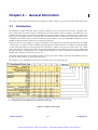
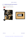
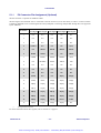
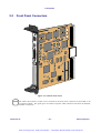
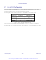
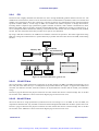
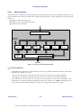
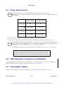
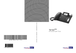
1
Artisan Technology Group is your source for quality new and certified-used/pre-owned equipment • FAST SHIPPING AND DELIVERY • TENS OF THOUSANDS OF IN-STOCK ITEMS • EQUIPMENT DEMOS • HUNDREDS OF MANUFACTURERS SUPPORTED • LEASING/MONTHLY RENTALS • ITAR CERTIFIED SECURE ASSET SOLUTIONS SERVICE CENTER REPAIRS Experienced engineers and technicians on staff at our full-service, in-house repair center WE BUY USED EQUIPMENT Sell your excess, underutilized, and idle used equipment We also offer credit for buy-backs and trade-ins www.artisantg.com/WeBuyEquipment InstraView REMOTE INSPECTION LOOKING FOR MORE INFORMATION? Visit us on the web at www.artisantg.com for more information on price quotations, drivers, technical specifications, manuals, and documentation SM Remotely inspect equipment before purchasing with our interactive website at www.instraview.com Contact us: (888) 88-SOURCE | [email protected] | www.artisantg.com ä Since March 6th, 2008 Thales Computers has become Kontron Modular Computers S.A. This documentation was created with Thales graphics rules. The Kontron Corporate Design will be implemented in the next version of this document. Each occurence of Thales Computers" shall be understood as Kontron Modular Computers S.A." For all questions related to this document, please contact support−kom−[email protected] or visit www.kontron.com Artisan Technology Group - Quality Instrumentation ... Guaranteed | (888) 88-SOURCE | www.artisantg.com THALES COMPUTERS ➜ Where COTS Meets Reality VMPC6a or VMPC6a-Dual PowerPC VME64 Boards - User's Guide CA.DT.129-5eĄĊĄJune 2003 www.thalescomputers.com Artisan Technology Group - Quality Instrumentation ... Guaranteed | (888) 88-SOURCE | www.artisantg.com Thales Computers, The Ruggedizer, UNI/RT and POWERENGINE are registered trademarks of Thales Computers S.A. – PowerPC, AIX, AIXwindows, RISC System/6000, IBM are registered trademarks of IBM Corp. –Linux is a registered trademark of Linus Torwards. – Red Hat is a registered trademark of Red Hat, Inc. – LynxOS is a registered trademark of LynuxWorks, Inc. – TORNADO and VxWorks are registered trademarks of Wind River System, Inc. – UNIX is a registered trademark licensed exclusively by X/Open Company Limited. – All other product names, trademarks and registered trademark are the property of their respective holders. Copyright Thales Computers 1987 – 2003 Thales Computers reserves the right to make changes further notice to any products herein, Thales Computers makes no warranty, representation or guarantee regarding the suitability of its products for any particular purpose, nor does Thales Computers assume any liability arising out of the application or user of any product or circuit, and specifically disclaims any and all liability, including without limitation consequential or incidental damages. “Typical” parameters can and do vary in different applications. All operating parameters including “Typicals” must be validated for each customer application by customer’s technical experts. Thales Computers does not convey any license under its patent rights nor the rights others. Thales Computers products are not designed, intended, or authorized for use as components in systems intended for surgical implant into body, or other applications intended to support or sustain life, or for any other application in which the failure of the Thales Computers product could create a situation where personal injury or death may occur. Should Buyer purchase or use Thales Computers products for any such unintended or unauthorized application, Buyer shall indemnify and hold Thales Computers and its officers, employees, subsidiaries, affiliates, and distributors harmless against all claims, costs, damages, and expenses, and reasonable attorney fees arising out of, directly or indirectly, any claim of personal injury or death associated with such unintended or unauthorized use, even if such claim alleges that Thales Computers was negligent regarding the design or manufacture of the part. Restricted Rights Legend Use, duplication or disclosure by the contractor or the Government is subject to restrictions as set forth in subdivision (b) (3)(ii) of the Rights in Technical Data and Computer Software clause 52.227–7013. No communication, reproduction or use without prior written approval from Thales Computers Your comments on this manual will be welcome. A sheet is appended for you to submit your remarks. Artisan Technology Group - Quality Instrumentation ... Guaranteed | (888) 88-SOURCE | www.artisantg.com Table Of Contents Chapter 1 – Introduction . . . . . . . . . . . . . . . . . . . . . . . . . . . . . . . . . . . . . . . . . . . . . . . . . . . . . . . . . . . . . 1 1.1 Objectives . . . . . . . . . . . . . . . . . . . . . . . . . . . . . . . . . . . . . . . . . . . . . . . . . . . . . . . . . . . . . . . . . . . . . . . . . . 2 1.2 Audience . . . . . . . . . . . . . . . . . . . . . . . . . . . . . . . . . . . . . . . . . . . . . . . . . . . . . . . . . . . . . . . . . . . . . . . . . . . 2 1.3 Scope . . . . . . . . . . . . . . . . . . . . . . . . . . . . . . . . . . . . . . . . . . . . . . . . . . . . . . . . . . . . . . . . . . . . . . . . . . . . . . 2 1.4 Structure . . . . . . . . . . . . . . . . . . . . . . . . . . . . . . . . . . . . . . . . . . . . . . . . . . . . . . . . . . . . . . . . . . . . . . . . . . . 2 1.5 Conventions . . . . . . . . . . . . . . . . . . . . . . . . . . . . . . . . . . . . . . . . . . . . . . . . . . . . . . . . . . . . . . . . . . . . . . . . . 3 1.6 Related Documents . . . . . . . . . . . . . . . . . . . . . . . . . . . . . . . . . . . . . . . . . . . . . . . . . . . . . . . . . . . . . . . . . . . 4 Chapter 2 – General Information . . . . . . . . . . . . . . . . . . . . . . . . . . . . . . . . . . . . . . . . . . . . . . . . . . . . . . 5 2.1 Introduction . . . . . . . . . . . . . . . . . . . . . . . . . . . . . . . . . . . . . . . . . . . . . . . . . . . . . . . . . . . . . . . . . . . . . . . . 5 2.2 Features . . . . . . . . . . . . . . . . . . . . . . . . . . . . . . . . . . . . . . . . . . . . . . . . . . . . . . . . . . . . . . . . . . . . . . . . . . . . 7 2.3 Inputs/Outputs . . . . . . . . . . . . . . . . . . . . . . . . . . . . . . . . . . . . . . . . . . . . . . . . . . . . . . . . . . . . . . . . . . . . . . 8 2.4 Operating System Support . . . . . . . . . . . . . . . . . . . . . . . . . . . . . . . . . . . . . . . . . . . . . . . . . . . . . . . . . . . . 9 Chapter 3 – Unpacking and Identification . . . . . . . . . . . . . . . . . . . . . . . . . . . . . . . . . . . . . . . . . . . . . . 11 3.1 Unpacking . . . . . . . . . . . . . . . . . . . . . . . . . . . . . . . . . . . . . . . . . . . . . . . . . . . . . . . . . . . . . . . . . . . . . . . . . . 11 3.2 Inspection . . . . . . . . . . . . . . . . . . . . . . . . . . . . . . . . . . . . . . . . . . . . . . . . . . . . . . . . . . . . . . . . . . . . . . . . . . 11 3.3 Board Identification . . . . . . . . . . . . . . . . . . . . . . . . . . . . . . . . . . . . . . . . . . . . . . . . . . . . . . . . . . . . . . . . . . 12 Chapter 4 – Hardware Configuration . . . . . . . . . . . . . . . . . . . . . . . . . . . . . . . . . . . . . . . . . . . . . . . . . . 13 4.1 Manufacturing Self–Test Link (LK1) . . . . . . . . . . . . . . . . . . . . . . . . . . . . . . . . . . . . . . . . . . . . . . . . . . . . 14 4.2 System Flash EPROM Link (LK2) . . . . . . . . . . . . . . . . . . . . . . . . . . . . . . . . . . . . . . . . . . . . . . . . . . . . . 15 4.3 User Flash EPROM Link (LK3) . . . . . . . . . . . . . . . . . . . . . . . . . . . . . . . . . . . . . . . . . . . . . . . . . . . . . . . . 16 4.4 Table Of Default Link Settings . . . . . . . . . . . . . . . . . . . . . . . . . . . . . . . . . . . . . . . . . . . . . . . . . . . . . . . . . 16 Chapter 5 – Connectors . . . . . . . . . . . . . . . . . . . . . . . . . . . . . . . . . . . . . . . . . . . . . . . . . . . . . . . . . . . . . . 17 5.1 Onboard Connectors . . . . . . . . . . . . . . . . . . . . . . . . . . . . . . . . . . . . . . . . . . . . . . . . . . . . . . . . . . . . . . . . . 5.1.1 P0 Connector Pin Assignment (Optional) . . . . . . . . . . . . . . . . . . . . . . . . . . . . . . . . . . . . . . . . . . . . . . . 5.1.2 P1 and P2 Row B (VMEbus) Connector Pin Assignment . . . . . . . . . . . . . . . . . . . . . . . . . . . . . . . . . . 5.1.3 Geographical Address Pin Assignment . . . . . . . . . . . . . . . . . . . . . . . . . . . . . . . . . . . . . . . . . . . . . . . . . 5.1.4 VMEbus Signal Description . . . . . . . . . . . . . . . . . . . . . . . . . . . . . . . . . . . . . . . . . . . . . . . . . . . . . . . . . 5.1.5 P2 Connector Pin Assignment . . . . . . . . . . . . . . . . . . . . . . . . . . . . . . . . . . . . . . . . . . . . . . . . . . . . . . . 5.1.6 P2 Signal Descriptions . . . . . . . . . . . . . . . . . . . . . . . . . . . . . . . . . . . . . . . . . . . . . . . . . . . . . . . . . . . . . 5.1.7 PMC Connector Pin Assignment . . . . . . . . . . . . . . . . . . . . . . . . . . . . . . . . . . . . . . . . . . . . . . . . . . . . . 5.1.7.1 J11 PMC Connector Pin Assignment . . . . . . . . . . . . . . . . . . . . . . . . . . . . . . . . . . . . . . . . . . 5.1.7.2 J12 PMC Connector Pin Assignment . . . . . . . . . . . . . . . . . . . . . . . . . . . . . . . . . . . . . . . . . . 5.1.7.3 J13 PMC Connector Pin Assignment . . . . . . . . . . . . . . . . . . . . . . . . . . . . . . . . . . . . . . . . . . 5.1.7.4 J14 PMC Connector Pin Assignment . . . . . . . . . . . . . . . . . . . . . . . . . . . . . . . . . . . . . . . . . . Thales Computers – i– 17 18 19 21 22 24 25 27 27 28 29 30 CA.DT.129–5e Artisan Technology Group - Quality Instrumentation ... Guaranteed | (888) 88-SOURCE | www.artisantg.com Table Of Contents 5.1.8 5.1.9 5.1.10 5.1.11 PMC Signal Description . . . . . . . . . . . . . . . . . . . . . . . . . . . . . . . . . . . . . . . . . . . . . . . . . . . . . . . . . . . . P7 CPU0 RISCWatch Connector Pin Assignment . . . . . . . . . . . . . . . . . . . . . . . . . . . . . . . . . . . . . . . . P8 CPU1 RISCWatch Connector Pin Assignment . . . . . . . . . . . . . . . . . . . . . . . . . . . . . . . . . . . . . . . . P7 and P8 Signal Description . . . . . . . . . . . . . . . . . . . . . . . . . . . . . . . . . . . . . . . . . . . . . . . . . . . . . . . . 31 33 34 35 5.2 Front Panel Connectors . . . . . . . . . . . . . . . . . . . . . . . . . . . . . . . . . . . . . . . . . . . . . . . . . . . . . . . . . . . . . . . 5.2.1 P3 Keyboard and Mouse Connector (KBD/MS) . . . . . . . . . . . . . . . . . . . . . . . . . . . . . . . . . . . . . . . . . 5.2.2 P4 Serial Connector (SERIAL) . . . . . . . . . . . . . . . . . . . . . . . . . . . . . . . . . . . . . . . . . . . . . . . . . . . . . . 5.2.2.1 SERIAL Connector with One Full Modem Serial Channel . . . . . . . . . . . . . . . . . . . . . . . . . 5.2.2.2 SERIAL Connector with Two Simplified Serial Channels . . . . . . . . . . . . . . . . . . . . . . . . . . 5.2.3 P5 SCSI–3 Connector (SCSI) . . . . . . . . . . . . . . . . . . . . . . . . . . . . . . . . . . . . . . . . . . . . . . . . . . . . . . . . 5.2.4 P6 ETHERNET 10BASE–T/100BASE–T Connector (ETHERNET) . . . . . . . . . . . . . . . . . . . . . . . . . 36 37 38 38 39 40 42 Chapter 6 – PMC Site . . . . . . . . . . . . . . . . . . . . . . . . . . . . . . . . . . . . . . . . . . . . . . . . . . . . . . . . . . . . . . . 43 6.1 Information Needed . . . . . . . . . . . . . . . . . . . . . . . . . . . . . . . . . . . . . . . . . . . . . . . . . . . . . . . . . . . . . . . . . . 43 6.2 Voltage Keying Pins . . . . . . . . . . . . . . . . . . . . . . . . . . . . . . . . . . . . . . . . . . . . . . . . . . . . . . . . . . . . . . . . . . 44 6.3 PMC Installation . . . . . . . . . . . . . . . . . . . . . . . . . . . . . . . . . . . . . . . . . . . . . . . . . . . . . . . . . . . . . . . . . . . . 45 Chapter 7 – System Installation . . . . . . . . . . . . . . . . . . . . . . . . . . . . . . . . . . . . . . . . . . . . . . . . . . . . . . . 47 7.1 System Backplane Configuration . . . . . . . . . . . . . . . . . . . . . . . . . . . . . . . . . . . . . . . . . . . . . . . . . . . . . . . 47 7.2 Chassis Ground . . . . . . . . . . . . . . . . . . . . . . . . . . . . . . . . . . . . . . . . . . . . . . . . . . . . . . . . . . . . . . . . . . . . . . 47 7.3 3.3V Power Recommendations . . . . . . . . . . . . . . . . . . . . . . . . . . . . . . . . . . . . . . . . . . . . . . . . . . . . . . . . . 48 7.4 System Configuration Suggestions . . . . . . . . . . . . . . . . . . . . . . . . . . . . . . . . . . . . . . . . . . . . . . . . . . . . . . 48 Chapter 8 – Operating Instructions . . . . . . . . . . . . . . . . . . . . . . . . . . . . . . . . . . . . . . . . . . . . . . . . . . . . 49 8.1 Power–up . . . . . . . . . . . . . . . . . . . . . . . . . . . . . . . . . . . . . . . . . . . . . . . . . . . . . . . . . . . . . . . . . . . . . . . . . . 49 8.2 Reset Switch . . . . . . . . . . . . . . . . . . . . . . . . . . . . . . . . . . . . . . . . . . . . . . . . . . . . . . . . . . . . . . . . . . . . . . . . 49 8.3 LEDs . . . . . . . . . . . . . . . . . . . . . . . . . . . . . . . . . . . . . . . . . . . . . . . . . . . . . . . . . . . . . . . . . . . . . . . . . . . . . . 50 8.4 Memory Maps . . . . . . . . . . . . . . . . . . . . . . . . . . . . . . . . . . . . . . . . . . . . . . . . . . . . . . . . . . . . . . . . . . . . . . 8.4.1 Example of Memory Map Seen by the Processor . . . . . . . . . . . . . . . . . . . . . . . . . . . . . . . . . . . . . . . . . 8.4.2 Example of PCI Memory Space Seen by the 32–bit PCI Master . . . . . . . . . . . . . . . . . . . . . . . . . . . . . 8.4.3 Example of PCI Memory Space Seen by the 64–bit PCI Master . . . . . . . . . . . . . . . . . . . . . . . . . . . . . 8.4.4 Example of PCI I/O Space Seen by the 32–bit PCI Master . . . . . . . . . . . . . . . . . . . . . . . . . . . . . . . . . 8.4.5 Example of PCI I/O Space Seen by the 64–bit PCI Master . . . . . . . . . . . . . . . . . . . . . . . . . . . . . . . . . 8.4.6 Memory Space . . . . . . . . . . . . . . . . . . . . . . . . . . . . . . . . . . . . . . . . . . . . . . . . . . . . . . . . . . . . . . . . . . . . 51 53 53 54 54 54 54 8.5 Interrupts and Error Reporting . . . . . . . . . . . . . . . . . . . . . . . . . . . . . . . . . . . . . . . . . . . . . . . . . . . . . . . . 8.5.1 Types of Reset . . . . . . . . . . . . . . . . . . . . . . . . . . . . . . . . . . . . . . . . . . . . . . . . . . . . . . . . . . . . . . . . . . . . 8.5.1.1 Hard Reset . . . . . . . . . . . . . . . . . . . . . . . . . . . . . . . . . . . . . . . . . . . . . . . . . . . . . . . . . . . . . . . 8.5.1.2 Soft Reset . . . . . . . . . . . . . . . . . . . . . . . . . . . . . . . . . . . . . . . . . . . . . . . . . . . . . . . . . . . . . . . . 8.5.2 Machine Check Exception . . . . . . . . . . . . . . . . . . . . . . . . . . . . . . . . . . . . . . . . . . . . . . . . . . . . . . . . . . 8.5.3 External Interrupt (INT*) . . . . . . . . . . . . . . . . . . . . . . . . . . . . . . . . . . . . . . . . . . . . . . . . . . . . . . . . . . . 8.5.4 System Management Interrupt (SMI*) . . . . . . . . . . . . . . . . . . . . . . . . . . . . . . . . . . . . . . . . . . . . . . . . . 8.5.5 External Device Interrupts (INTEXT*) . . . . . . . . . . . . . . . . . . . . . . . . . . . . . . . . . . . . . . . . . . . . . . . . 8.5.6 PCI Interrupts . . . . . . . . . . . . . . . . . . . . . . . . . . . . . . . . . . . . . . . . . . . . . . . . . . . . . . . . . . . . . . . . . . . . 55 56 56 56 57 57 57 57 59 8.6 32–bit PCI Configuration . . . . . . . . . . . . . . . . . . . . . . . . . . . . . . . . . . . . . . . . . . . . . . . . . . . . . . . . . . . . . 60 8.7 64–bit PCI Configuration . . . . . . . . . . . . . . . . . . . . . . . . . . . . . . . . . . . . . . . . . . . . . . . . . . . . . . . . . . . . . 61 CA.DT.129–5e – ii – Thales Computers Artisan Technology Group - Quality Instrumentation ... Guaranteed | (888) 88-SOURCE | www.artisantg.com Table Of Contents Chapter 9 – Functional Description . . . . . . . . . . . . . . . . . . . . . . . . . . . . . . . . . . . . . . . . . . . . . . . . . . . . 63 9.1 VMPC6a Block Diagram . . . . . . . . . . . . . . . . . . . . . . . . . . . . . . . . . . . . . . . . . . . . . . . . . . . . . . . . . . . . . . 64 9.2 General Description . . . . . . . . . . . . . . . . . . . . . . . . . . . . . . . . . . . . . . . . . . . . . . . . . . . . . . . . . . . . . . . . . . 9.2.1 Host Bridge . . . . . . . . . . . . . . . . . . . . . . . . . . . . . . . . . . . . . . . . . . . . . . . . . . . . . . . . . . . . . . . . . . . . . . 9.2.2 Processor . . . . . . . . . . . . . . . . . . . . . . . . . . . . . . . . . . . . . . . . . . . . . . . . . . . . . . . . . . . . . . . . . . . . . . . . 9.2.3 Secondary Level Cache . . . . . . . . . . . . . . . . . . . . . . . . . . . . . . . . . . . . . . . . . . . . . . . . . . . . . . . . . . . . . 9.2.4 PCI . . . . . . . . . . . . . . . . . . . . . . . . . . . . . . . . . . . . . . . . . . . . . . . . . . . . . . . . . . . . . . . . . . . . . . . . . . . . . 9.2.4.1 32–bit PCI bus . . . . . . . . . . . . . . . . . . . . . . . . . . . . . . . . . . . . . . . . . . . . . . . . . . . . . . . . . . . . 9.2.4.2 64–bit PCI bus . . . . . . . . . . . . . . . . . . . . . . . . . . . . . . . . . . . . . . . . . . . . . . . . . . . . . . . . . . . . 9.2.4.3 PCI Carrier Card . . . . . . . . . . . . . . . . . . . . . . . . . . . . . . . . . . . . . . . . . . . . . . . . . . . . . . . . . 9.2.5 Memory . . . . . . . . . . . . . . . . . . . . . . . . . . . . . . . . . . . . . . . . . . . . . . . . . . . . . . . . . . . . . . . . . . . . . . . . . 9.2.5.1 SDRAM . . . . . . . . . . . . . . . . . . . . . . . . . . . . . . . . . . . . . . . . . . . . . . . . . . . . . . . . . . . . . . . . . 9.2.5.2 System Flash EPROM . . . . . . . . . . . . . . . . . . . . . . . . . . . . . . . . . . . . . . . . . . . . . . . . . . . . . . 9.2.5.3 NVRAM/RTC . . . . . . . . . . . . . . . . . . . . . . . . . . . . . . . . . . . . . . . . . . . . . . . . . . . . . . . . . . . . . 9.2.5.4 User Flash EPROM . . . . . . . . . . . . . . . . . . . . . . . . . . . . . . . . . . . . . . . . . . . . . . . . . . . . . . . . 9.2.6 VMEbus Interface . . . . . . . . . . . . . . . . . . . . . . . . . . . . . . . . . . . . . . . . . . . . . . . . . . . . . . . . . . . . . . . . . 9.2.6.1 VMEbus Master Access . . . . . . . . . . . . . . . . . . . . . . . . . . . . . . . . . . . . . . . . . . . . . . . . . . . . . 9.2.6.2 VMEbus Slave Access . . . . . . . . . . . . . . . . . . . . . . . . . . . . . . . . . . . . . . . . . . . . . . . . . . . . . . 9.2.6.3 VMEbus Arbitration . . . . . . . . . . . . . . . . . . . . . . . . . . . . . . . . . . . . . . . . . . . . . . . . . . . . . . . 9.2.6.4 DMA Channels . . . . . . . . . . . . . . . . . . . . . . . . . . . . . . . . . . . . . . . . . . . . . . . . . . . . . . . . . . . 9.2.6.5 Interrupt Management . . . . . . . . . . . . . . . . . . . . . . . . . . . . . . . . . . . . . . . . . . . . . . . . . . . . . . 9.2.7 Utility I/O and Auxiliary Function Bus . . . . . . . . . . . . . . . . . . . . . . . . . . . . . . . . . . . . . . . . . . . . . . . . 9.2.8 PCI 10/100–Mb/s Ethernet LAN Controller . . . . . . . . . . . . . . . . . . . . . . . . . . . . . . . . . . . . . . . . . . . . . 9.2.9 SCSI Controller . . . . . . . . . . . . . . . . . . . . . . . . . . . . . . . . . . . . . . . . . . . . . . . . . . . . . . . . . . . . . . . . . . . 9.2.10 Serial I/O Controller . . . . . . . . . . . . . . . . . . . . . . . . . . . . . . . . . . . . . . . . . . . . . . . . . . . . . . . . . . . . . . . 9.2.11 Keyboard and Mouse Controller . . . . . . . . . . . . . . . . . . . . . . . . . . . . . . . . . . . . . . . . . . . . . . . . . . . . . . 65 65 65 65 66 66 66 67 67 67 67 68 68 69 69 69 70 70 70 71 72 74 76 77 9.3 77 Temperature Control . . . . . . . . . . . . . . . . . . . . . . . . . . . . . . . . . . . . . . . . . . . . . . . . . . . . . . . . . . . . . . . . . Chapter 10 –VMPCBug Debugging Monitor . . . . . . . . . . . . . . . . . . . . . . . . . . . . . . . . . . . . . . . . . . . . . 79 10.1 Using The VMPCBug Debugger . . . . . . . . . . . . . . . . . . . . . . . . . . . . . . . . . . . . . . . . . . . . . . . . . . . . . . . . 79 10.2 Debugger Commands . . . . . . . . . . . . . . . . . . . . . . . . . . . . . . . . . . . . . . . . . . . . . . . . . . . . . . . . . . . . . . . . . 10.2.1 VPD Command . . . . . . . . . . . . . . . . . . . . . . . . . . . . . . . . . . . . . . . . . . . . . . . . . . . . . . . . . . . . . . . . . . . 10.2.2 CONF Command . . . . . . . . . . . . . . . . . . . . . . . . . . . . . . . . . . . . . . . . . . . . . . . . . . . . . . . . . . . . . . . . . . 10.2.3 DEV Command . . . . . . . . . . . . . . . . . . . . . . . . . . . . . . . . . . . . . . . . . . . . . . . . . . . . . . . . . . . . . . . . . . . 10.2.4 ENV Command . . . . . . . . . . . . . . . . . . . . . . . . . . . . . . . . . . . . . . . . . . . . . . . . . . . . . . . . . . . . . . . . . . . 79 82 82 87 87 Appendix A – Specifications . . . . . . . . . . . . . . . . . . . . . . . . . . . . . . . . . . . . . . . . . . . . . . . . . . . . . . . . . . . 89 A.1 VMEbus Compliance . . . . . . . . . . . . . . . . . . . . . . . . . . . . . . . . . . . . . . . . . . . . . . . . . . . . . . . . . . . . . . . . . 89 A.2 Local Resources . . . . . . . . . . . . . . . . . . . . . . . . . . . . . . . . . . . . . . . . . . . . . . . . . . . . . . . . . . . . . . . . . . . . . 90 A.3 Power Requirements . . . . . . . . . . . . . . . . . . . . . . . . . . . . . . . . . . . . . . . . . . . . . . . . . . . . . . . . . . . . . . . . . 91 A.4 EMC Regulatory Compliance and Reliability . . . . . . . . . . . . . . . . . . . . . . . . . . . . . . . . . . . . . . . . . . . . 91 A.5 Flammability Rating . . . . . . . . . . . . . . . . . . . . . . . . . . . . . . . . . . . . . . . . . . . . . . . . . . . . . . . . . . . . . . . . . 91 A.6 Environmental Specifications . . . . . . . . . . . . . . . . . . . . . . . . . . . . . . . . . . . . . . . . . . . . . . . . . . . . . . . . . . A.6.1 Operating Environment . . . . . . . . . . . . . . . . . . . . . . . . . . . . . . . . . . . . . . . . . . . . . . . . . . . . . . . . . . . . . A.6.2 Storage Environment . . . . . . . . . . . . . . . . . . . . . . . . . . . . . . . . . . . . . . . . . . . . . . . . . . . . . . . . . . . . . . . 92 92 92 Thales Computers – iii – CA.DT.129–5e Artisan Technology Group - Quality Instrumentation ... Guaranteed | (888) 88-SOURCE | www.artisantg.com Table Of Contents A.7 Mechanical Construction . . . . . . . . . . . . . . . . . . . . . . . . . . . . . . . . . . . . . . . . . . . . . . . . . . . . . . . . . . . . . 93 Appendix B – Troubleshooting . . . . . . . . . . . . . . . . . . . . . . . . . . . . . . . . . . . . . . . . . . . . . . . . . . . . . . . . . 95 B.1 Step 1 – No Power . . . . . . . . . . . . . . . . . . . . . . . . . . . . . . . . . . . . . . . . . . . . . . . . . . . . . . . . . . . . . . . . . . . 95 B.2 Step 2 – Power On, Unexpected Behaviour . . . . . . . . . . . . . . . . . . . . . . . . . . . . . . . . . . . . . . . . . . . . . . . 95 B.3 Step 3 – Power On, No Terminal Display . . . . . . . . . . . . . . . . . . . . . . . . . . . . . . . . . . . . . . . . . . . . . . . . 96 B.4 Step 4 – Overheating . . . . . . . . . . . . . . . . . . . . . . . . . . . . . . . . . . . . . . . . . . . . . . . . . . . . . . . . . . . . . . . . . 96 B.5 Step 5 – VMPC6a Locks–up . . . . . . . . . . . . . . . . . . . . . . . . . . . . . . . . . . . . . . . . . . . . . . . . . . . . . . . . . . . 96 B.6 Debugging . . . . . . . . . . . . . . . . . . . . . . . . . . . . . . . . . . . . . . . . . . . . . . . . . . . . . . . . . . . . . . . . . . . . . . . . . . 96 B.7 When Phoning, Faxing or E–Mailing to Technical Support, Be Prepared To Give . . . . . . . . . . . . . . 97 Glossary . . . . . . . . . . . . . . . . . . . . . . . . . . . . . . . . . . . . . . . . . . . . . . . . . . . . . . . . . . . . . . . . . . . . . . . . . . . 99 Index . . . . . . . . . . . . . . . . . . . . . . . . . . . . . . . . . . . . . . . . . . . . . . . . . . . . . . . . . . . . . . . . . . . . . . . . . . . . . . 105 CA.DT.129–5e – iv – Thales Computers Artisan Technology Group - Quality Instrumentation ... Guaranteed | (888) 88-SOURCE | www.artisantg.com Table Of Contents List Of Figures Figure 2.1: Top View of the VMPC6a . . . . . . . . . . . . . . . . . . . . . . . . . . . . . . . . . . . . . . . . . . . . . . . . . . . . . . . . . . . . . 6 Figure 2.2: Auxiliary I/O Connection . . . . . . . . . . . . . . . . . . . . . . . . . . . . . . . . . . . . . . . . . . . . . . . . . . . . . . . . . . . . . 8 Figure 4.1: VMPC6a Link Positions . . . . . . . . . . . . . . . . . . . . . . . . . . . . . . . . . . . . . . . . . . . . . . . . . . . . . . . . . . . . . . 13 Figure 5.1: Connector Positions and Numbering . . . . . . . . . . . . . . . . . . . . . . . . . . . . . . . . . . . . . . . . . . . . . . . . . . . . 17 Figure 5.2: VMPC6a Front Panel . . . . . . . . . . . . . . . . . . . . . . . . . . . . . . . . . . . . . . . . . . . . . . . . . . . . . . . . . . . . . . . . 36 Figure 9.1: VMPC6a Block Diagram . . . . . . . . . . . . . . . . . . . . . . . . . . . . . . . . . . . . . . . . . . . . . . . . . . . . . . . . . . . . . 64 Figure 9.2: PCI Interconnectivity (generic use) . . . . . . . . . . . . . . . . . . . . . . . . . . . . . . . . . . . . . . . . . . . . . . . . . . . . . 66 Figure 9.3: PCI to VME Bridge Block Diagram . . . . . . . . . . . . . . . . . . . . . . . . . . . . . . . . . . . . . . . . . . . . . . . . . . . . . 69 Figure 9.4: I/O Controller Block Diagram . . . . . . . . . . . . . . . . . . . . . . . . . . . . . . . . . . . . . . . . . . . . . . . . . . . . . . . . . 71 Figure 9.5: PCI 10/100–Mb/s Ethernet LAN Controller Block Diagram . . . . . . . . . . . . . . . . . . . . . . . . . . . . . . . . . . 72 Figure 9.6: SCSI Controller Block Diagram . . . . . . . . . . . . . . . . . . . . . . . . . . . . . . . . . . . . . . . . . . . . . . . . . . . . . . . . 74 Figure A.1: VME Dimensions . . . . . . . . . . . . . . . . . . . . . . . . . . . . . . . . . . . . . . . . . . . . . . . . . . . . . . . . . . . . . . . . . . . 93 Thales Computers – v– CA.DT.129–5e Artisan Technology Group - Quality Instrumentation ... Guaranteed | (888) 88-SOURCE | www.artisantg.com Table Of Contents List Of Tables Table 2.1: VMPC6a Order Code . . . . . . . . . . . . . . . . . . . . . . . . . . . . . . . . . . . . . . . . . . . . . . . . . . . . . . . . . . . . . . . . . 5 Table 6.1: PMC Site Information . . . . . . . . . . . . . . . . . . . . . . . . . . . . . . . . . . . . . . . . . . . . . . . . . . . . . . . . . . . . . . . . 43 Table 8.1: External Interrupts (INTEXT*) . . . . . . . . . . . . . . . . . . . . . . . . . . . . . . . . . . . . . . . . . . . . . . . . . . . . . . . . . 58 Table 8.2: Devices connected to the 32–bit PCI bus . . . . . . . . . . . . . . . . . . . . . . . . . . . . . . . . . . . . . . . . . . . . . . . . . . 60 Table 8.3: Devices connected to the 64–bit PCI bus . . . . . . . . . . . . . . . . . . . . . . . . . . . . . . . . . . . . . . . . . . . . . . . . . . 61 Table 10.1: Usual Commands . . . . . . . . . . . . . . . . . . . . . . . . . . . . . . . . . . . . . . . . . . . . . . . . . . . . . . . . . . . . . . . . . . . 81 CA.DT.129–5e – vi – Thales Computers Artisan Technology Group - Quality Instrumentation ... Guaranteed | (888) 88-SOURCE | www.artisantg.com Chapter 1 – Introduction The VMPC6a board with its associated peripherals and software, is the latest generation of product in Thales Computers’s POWERENGINE family based on VME PowerPC boards. With this new generation, Thales Computers confirms its leadership in the arena of PowerPC Real–Time Systems, as the first supplier of PowerPC VME SBC’s (beginning in November 1993). Designed for users who require scalable, high performance processors, sophisticated I/O subsystems and high levels of on–board integration, the VMPC6a offers a cost–effective solution to a wide range of application requirements. Based on the industry standard PowerPC architecture, the VMPC6a with one or two PowerPC 750L RISC CPUs onboard offers a choice of processor frequencies starting at 450 MHz. The VMPC6a is based on the highly integrated host bridge AVIGNON (named CPC710 by IBM) which interfaces the system bus running at 100 MHz and upwards to both a 32–bit and a 64–bit PCI bus. The board provides 1 MB of L2 cache connected directly on each processor via a 64–bit backside L2 cache bus with an operating frequency corresponding to half the CPU frequency, up to 512 MB of onboard high–performance Synchronous DRAM combined with Error Checking and Correcting (ECC) for high system integrity, System and User Flashes and also an interrupt controller. Local connection of Wide Ultra SCSI, 10/100BASE–T Ethernet interface, keyboard/mouse interface and VME64 bus use the 32–bit PCI bus. With its IEEE P1386.1 PMC site, allowing 64–bit 66 MHz PCI operations, the number of PMC sites can be expanded from one on–board up to three by using a companion carrier card (ICPMC–6). PMCs available directly from Thales Computers include high performance graphics, ATM, fast Ethernet, asynchronous serial lines and MIL–STD–1553B, with a wide range of other PMC types available from Third Parties. Additional I/Os for twin serial and PMC I/Os are also available. Thales Computers proposes a complete solution providing customers with a single interface from the development environment to the Target Board Computer, from the system software right through to hardware and system. For example, Thales Computers offers full support for multihead graphics systems based on the POWERENGINE: Thales Computers PowerPC single board computer coupled with several graphics PMC modules. Thales Computers cluster architecture allows the cohabitation on a single bus of several POWERENGINE VME CPU’s, each executing an OS (AIX, LynxOS, VxWorks) and dialoguing by means of a TCP/IP type mechanism or by message passing over the VME backplane. By exercising full control over the source code of the system software offering, Thales Computers is able to guarantee perfect interoperability: ' Thales Computers is a source code licensee for both AIX and LynxOS. ' UNIX Operating System, AIX compatible with IBM RS/6000. ' LynxOS, a POSIX conformant Real–Time OS with single and multiprocessing. X11, MOTIF, TCP/IP are supported. Native and cross development environments are available (C, C++, FORTRAN, ADA). ' Wind River VxWorks BSP and associated development environments. ' Other OSs available through Third Parties due to PReP compliance. The VMPC6a supports several environment condition severity, from the standard “S” class build up (0 to 55 degrees, air cooled) to the Ruggedized “RC” build up (–40 to +55 degrees, conduction cooled). Typical applications for such a highly attractive product in terms of performance, price and flexible I/O are military, communications, image and signal processing, medical, industrial process control, C3I, scientific research and many others. Thales Computers –1– CA.DT.129–5e Artisan Technology Group - Quality Instrumentation ... Guaranteed | (888) 88-SOURCE | www.artisantg.com Introduction 1.1 Objectives This guide provides general information, hardware preparation and installation instructions, operating instructions and a functional description of the VMPC6a board. The onboard programming, onboard firmware and other firmware (e.g. drivers and BSPs) are described in detail in separate guides (see section 1.6 “Related Documents”). 1.2 Audience This guide is written to cover, as far as possible, the range of people who will handle or use the VMPC6a, from unpackers/inspectors, through system managers and installation technicians to hardware and software engineers. Most chapters assume a certain amount of knowledge on the subjects of single board computer architecture, interfaces, peripherals, systems, cabling, grounding, VME and communications. There is a glossary provided at the back of this guide that explains some of the terms used and expands all abbreviations. 1.3 Scope This guide describes all variants of the VMPC6a. It does not cover any daughter boards, PMC modules or the carrier card which are described in specific guides (see section 1.6 “Related Documents”). 1.4 Structure This guide is structured in a way that will reflect the sequence of operations from receipt of the board up to getting it working in your system. Each topic is covered in a separate chapter and each chapter begins with a brief introduction that tells you what the chapter contains. In this way, you can skip any chapters that are not applicable or with which you are already familiar. The chapters are: ` Chapter 1 (this chapter) – gives a brief introduction, this guide’s objectives and audience, the structure, some warnings, conventions and related documentation. ` Chapter 2 – is a VMPC6a general information. ` Chapter 3 – contains unpacking, inspection and identification instructions. ` Chapter 4 – describes the board configuration. ` Chapter 5 – describes the board’s connectors and signals used. ` Chapter 6 – describes the mezzanine boards and PMC installation. ` Chapter 7 – describes installation of the board in a system. ` Chapter 8 – describes power–up and subsequent operation of the board. ` Chapter 9 – is a functional description. ` Chapter 10 – gives an overview of the VMPCBug Debugging Monitor’s commands. ` Appendix A – is a board specification. ` Appendix B – gives troubleshooting guidelines. There are also a glossary and an index provided. CA.DT.129–5e –2– Thales Computers Artisan Technology Group - Quality Instrumentation ... Guaranteed | (888) 88-SOURCE | www.artisantg.com Introduction 1.5 Conventions All numbers are expressed in decimal, except addresses and memory or register data, which are expressed in hexadecimal. The prefix ‘0x’ shows a hexadecimal number, following the ‘C’ programming language convention. Information of particular importance is in bold typeface and is further highlighted by the WARNING box. General information is sometimes in bold typeface and is further highlighted by the NOTE box. NOTE The multipliers ‘k’, ‘M’ and ‘G’ have their conventional scientific and engineering meanings of *103, *106 and *109 respectively. The only exception to this is in the description of the size of memory areas, when ‘K’, ‘M’ and ‘G’ mean *210, *220 and *230 respectively. 3 6 9 10 20 30 NOTE When describing transfer rates, ‘k’ ‘M’ and ‘G’ mean *10 , *10 and *10 not *2 *2 and *2 . In PowerPC terminology, multiple bit fields are numbered from 0 to n, where 0 is the MSB and n is the LSB. PCI and VMEbus terminology follows the more familiar convention that bit 0 is the LSB and n is the MSB. Signal names ending with an asterisk (*) denote active low signals; all other signals are active high. Following the PCI convention, signal names ending with a # denote active low signals; all other signals are active high. The term VMPC6a is used generically to refer to the VMPC6a (using one PowerPC 750l) and VMPC6a–Dual (using two PowerPC 750L) boards. The devices are specifically referenced where necessary. Thales Computers –3– CA.DT.129–5e Artisan Technology Group - Quality Instrumentation ... Guaranteed | (888) 88-SOURCE | www.artisantg.com Introduction 1.6 Related Documents Due to the complexity of some of the devices used on VMPC6a, you will need to refer to the following documents for more detailed information. - Thales Computers Documentations ` VMPC6a or VMPC6a–Dual Board – Hardware Release Notes, publication number CA.DT.328. ` VMPC6 Boards – Connection Guide, publication number CA.DT.319. ` VMPC6 Boards – Programmer’s Reference Guide, publication number CA.DT.318. ` Supplement for VMPC6a/RA or VMPC6a–Dual/RA Boards – User’s Guide, publication number CA.DT.132. ` VMPC6a/RC or VMPC6a–Dual/RC Boards – User’s Guide, publication number CA.DT.128. ` Self–Tests for VMPC6 Boards – User’s Manual, publication number CA.DT.320. ` Release Notes VMPCBug and Self–Tests, publication number SD.DT.A51. ` VMPCBug User’s Manual, publication number SD.DT.A35. ` CPCIGx Board – Thales Computers Graphics Mezzanine Board, publication number CA.DT.118. ` ICPMC–6 Board – Thales Computers PMC Carrier Board for VMPC6 Boards, publication number CA.DT.130. ` COBRA Interrupts and I/O Controller, Reference Manual, publication number CI.DT.405. NOTE The publication numbers of the AIX and LynxOS documentations are not listed because they depend on the AIX and LynxOS version distributed with your board. - Other Documentations ` VME64 Specification ANSI/VITA 1–1994. ` VME64 Extensions ANSI/VITA 1.1–1997. ` PCI Local Bus Specification Revision 2.2 december 18, 1998, PCI Special Interest Group. ` PCI System Design Guide Rev 1.0 9/93, PCI Special Interest Group. ` PowerPC Reference Platform (PReP) Specification, Version 1.1, IBM. ` PowerPC Architecture Books I, II, III and IV, Motorola Inc., IBM. ` MPC750, RISC Processor User’s Manual, Motorola Inc., publication number MPC750UM/AD. ` SYM53C875 PCI–SCSI I/O Processor with UltraSCSI Data Manual, Revision 2.0, Symbios Logic Inc. ` Digital Semiconductor 21143 PCI/CardBus 10/100–Mb/s Ethernet LAN Controller, Data Sheet, Order Number EC–QWC3B–TE. ` Digital Semiconductor 21143 PCI/CardBus 10/100–Mb/s Ethernet LAN Controller, Hardware Reference Manual Order Number EC–QWC4B–TE. ` CPC710 (AVIGNON): PowerPC chip support with dual PCI 32–64 Bridge & SDRAM Controller, IBM. ` ALMA_V64 – PCI to VME Bridge Data Sheet, IBM, March 1998. ` IEEE P1386 Draft Standard for a Common Mezzanine Card Family: CMC. ` IEEE P1386.1 Draft Standard Physical and Environmental Layers for PCI Mezzanine Cards: PMC. ` M48T18 CMOS 8Kx8 TIMEKEEPER SRAM Data Sheet, SGS–Thomson, publication number M48T18 (on VMPC6a). ` M48T59 CMOS 8Kx8 TIMEKEEPER SRAM Data Sheet, SGS–Thomson, publication number M48T59 (on VMPC6a/RA). ` Tl16C550C Asynchronous Communications Element with Autoflow Control, Texas Instruments, publication number SLLS177E. CA.DT.129–5e –4– Thales Computers Artisan Technology Group - Quality Instrumentation ... Guaranteed | (888) 88-SOURCE | www.artisantg.com Chapter 2 – General Information This chapter contains general information for the VMPC6a product. Chapter 9 gives a functional description of the board. 2.1 Introduction The VMPC6a is a highly integrated, PReP compatible VMEbus processor card based on the PowerPC 750L RISC CPU. This product offers an extensive range of standard functions and expansion options including: one (VMPC6a) or two (VMPC6a–Dual) processor(s) clocked from 450 MHz and upwards, secondary cache of 1 MB per processor, onboard user memory up to 512 MBytes with ECC, onboard serial and Ethernet channels, 1.5 MBytes of system Flash memory, up to 32 MBytes of user Flash memory, a Wide Ultra SCSI peripheral interface, a 64–bit 66 MHz PMC module site, a 64–bit VMEbus interface and direct connection for a keyboard and mouse. With the PCI carrier card (ICPMC–6), expansion capabilities are provided for up to three PCI interface slots. PCI (PMC – IEEE P1386.1) provides an industry standard, high speed (from 132 Mbytes/second to 533 Mbytes/seconds depending on data width and frequency) local expansion bus, designed for graphics, high–speed communications (e.g. ATM), multi–media and user–defined custom functions. PCI has established itself as the leading local interconnect standard, and the wide availability of compatible devices, coupled with its adoption on an array of platforms, ensures that PCI based modules offer both high–performance and low cost. The highly integrated nature of the VMPC6a makes it a true single board computer, and allows the VME64 interface to become an optional feature for appropriate applications. The VMPC6a comes with different build options which are listed in the following table: Table 2.1: VMPC6a Order Code Thales Computers –5– CA.DT.129–5e Artisan Technology Group - Quality Instrumentation ... Guaranteed | (888) 88-SOURCE | www.artisantg.com General Information ÖÖÖÖÖÖ ÖÖÖÖÖÖ ÖÖÖÖÖÖ ÖÖÖÖÖÖÖÖ Ö ÖÖ ÖÖ ÖÖ ÖÖ ÖÖ ÖÖ ÖÖ ÖÖ ÖÖ ÖÖÖ SRAM CPU0 SRAM CPU1 PPC750 CPU0 PPC750 CPU1 SRAM CPU1 NVRAM SRAM CPU0 AVIGNON (CPC710) Host Bridge ALMA_V64 VME–PCI INTERFACE COBRA Interrupt and I/O Controller USB Cont. P1 P0 USER FLASH 1 Ö ÖÖ Ö ÖÖ Ö ÖÖ ÖÖ Ö ÖÖ ÖÖ Ö ÖÖ ÖÖ Ö ÖÖ ÖÖ ÖÖ ÖÖÖ ÖÖÖ ÖÖ ÖÖ Ö ÖÖ ÖÖ Ö ÖÖ Ö ÖÖ ÖÖÖÖÖÖ 1 SCSI SCSI CONTROLLER Terminators 10/100BASE–T Controller 1 First System Flash 10/100BASE–T Transformer 10/100BASE–T Transceiver 1 P2 1 NOTE Onboard SDRAM and the second System Flash are on the bottom side. Figure 2.1: Top View of the VMPC6a CA.DT.129–5e –6– Thales Computers Artisan Technology Group - Quality Instrumentation ... Guaranteed | (888) 88-SOURCE | www.artisantg.com General Information 2.2 Features D PowerPC: one 750L processor from 450 MHz and upwards for VMPC6a, two 750L processors from 450 MHz and upwards for VMPC6a–Dual. D Extensive operating system support, including AIX, LynxOS and VxWorks D Wide range of shrink–wrapped application software available D 1 MByte of 2 way set associative secondary cache per processor D One 64–bit 66/33 MHz PCI/PMC expansion slot onboard, with optional carrier (ICPMC–6) providing a maximum of three PCI/PMC slots D Up to 512 MBytes of SDRAM with ECC onboard D 1.5 MBytes of System Flash EPROM D 8Kx8 of user NVRAM and Real Time Clock (TOD/calendar) with a replaceable battery/crystal package D Standard features include: Onboard PCI Ethernet LAN controller with 10/100BASE–T Ethernet on front panel, Up to 32 MBytes of User Flash EPROM, Ultra or Wide Ultra SCSI I/O processor, Two RS232 serial I/O channels up to 115.2 Kbaud, Keyboard/mouse interface, VME64 interface with PCI to VME64 bridge, using ALMA_V64 PCI to VME interface chip, Local I/Os and PMC I/Os routed to P2 connector. D VME64 interface: ALMA_V64 PCI to VME bridge, VME64 master/slave capability, Full VME system controller and interrupt generator/handler capability, Flexible address mapping, Two DMA channels, Hardware semaphores for multiprocessing. D Manufacturing option: User Flash sizes: 8 or 32 MB, SDRAM size: 64, 128, 256 or 512 MB, V(I/O) PMC: +3.3 V for the PCI/PMC slot, Ethernet routed to backplane. P0 connector available. D Single slot 6U VME64x board D ANSI/VITA 1–1994 VME64 compliant D ANSI/VITA 1.1– 1997 VME64 Extensions Thales Computers –7– CA.DT.129–5e Artisan Technology Group - Quality Instrumentation ... Guaranteed | (888) 88-SOURCE | www.artisantg.com General Information 2.3 Inputs/Outputs The VMPC6a has a wide variety of possible I/O connectivity including Wide Ultra SCSI, Ethernet, serial and mouse/keyboard ports. The front panel can provide one keyboard and mouse port, one 10/100BASE–T Ethernet port and one SCSI–3 port. In addition, a firmware configuration enables to select either one RS232 serial I/O channel on one connector or both RS232 serial I/O channels on the same connector (for more information about this configuration refer to section 10.2.2 page 82). For more information about the pin assignment of the front panel connectors, refer to section 5.2 page 36. The VMPC6a P2 connector can provide Local I/Os (Ultra or Wide Ultra SCSI, asynchronous serial lines and mouse/keyboard ports) and PMC I/Os. As a manufacturing option, the 10/100BASE–T Ethernet port could be available on P2 connector, replacing the Ethernet front panel connectivity. For more information about the P2 pin assignment refer to section 5.1.5 page 24. Using P2 I/O minimizes the effort needed to remove boards from a rack, improving maintainability and reliability. For example the P2 I/Os may be attached by a VME64 P2 transition module (CP2IOW5RU), refer to the Connection Guide” for more information about the P2 transition module pin assignments. ÖÖÖÖ ÖÖÖÖÖ Ö Ö Ö Ö Ö Ö Ö Ö Ö Ö Ö Ö Ö Ö ÖÖÖ ÖÖÖ Ö Ö ÖÖ ÖÖ Ö P1 16–bit SCSI connector ÖÖ Ö Ö ÖÖ Ö ÖÖ Ö ÖÖ Ö Ö ÖÖ Ö Ö ÖÖ Ö Ö Ö Ö ÖÖ Ö ÖÖ CP2IOW5RU P2 PMC IO connector 10/100ASE–T Ethernet connector Keyboard/Mouse connector COBRA GPIO connector Serial line connector Figure 2.2: Auxiliary I/O Connection CA.DT.129–5e –8– Thales Computers Artisan Technology Group - Quality Instrumentation ... Guaranteed | (888) 88-SOURCE | www.artisantg.com General Information 2.4 Operating System Support The following operating systems are supported on the VMPC6a as Thales Computers standard products: AIX, LynxOS and VxWorks/Tornado. Contact Thales Computers for more information. Thales Computers –9– CA.DT.129–5e Artisan Technology Group - Quality Instrumentation ... Guaranteed | (888) 88-SOURCE | www.artisantg.com General Information CA.DT.129–5e – 10 – Thales Computers Artisan Technology Group - Quality Instrumentation ... Guaranteed | (888) 88-SOURCE | www.artisantg.com Chapter 3 – Unpacking and Identification This chapter gives guidelines on unpacking, inspecting and identifying the VMPC6a. CAUTION THIS PRODUCT IS CLASS 1 ELECTROSTATIC DISCHARGE SENSITIVE. USE ESD PRECAUTIONARY MEASURES WHEN HANDLING IT 3.1 Unpacking Thales Computers boards are protected by an antistatic envelope. Observe antistatic precautions and work at an approved antistatic work station when unpacking the board. The VMPC6a is shipped in an individual, reusable shipping box. When you receive the shipping container, inspect it for any evidence of physical damage. If the container is damaged, request that the carrier’s agent is present when the carton is opened. Keep the contents and packing materials for the agent’s inspection and notify Thales Computers customer service department of the incident. Retain the packing list for reference. Assuming that there is no obvious damage, you may still want to keep the shipping carton in case you want to ship the VMPC6a on elsewhere. This package has been designed for shipping and it is not suitable for long–term storage nor storage under severe conditions. Fore more information, please visit our web site: www.thalescomputers.com/readfirst/ . 3.2 Inspection Assuming that the VMPC6a is not obviously damaged, you can now go on to inspect it. It is possible for components (connectors, socketed chips etc.) to work loose or be dislodged in transit or in the process of unpacking, although this is extremely unlikely. A quick visual inspection should reveal any obviously loose components. Any defects detected should be reported to Thales Computers. Thales Computers – 11 – CA.DT.129–5e Artisan Technology Group - Quality Instrumentation ... Guaranteed | (888) 88-SOURCE | www.artisantg.com Unpacking and Identification 3.3 Board Identification Thales Computers VMPC6a boards are identified by labels fitted on the bottom side. - Labels fitted to the bottom side of the VMPC6a: A “Commercial Reference” label of the mother board. Refer to Chapter 2: “General Information”, section 2.1 “Introduction”, Table 2.1 “VMPC6a Order Code” on page 5 for a complete description of this label. B “Board Idenditification” label of the mother board. C “Variant” label and “Engineering Change Level” (E.C. Level) label. The “Variant” label is used with the Self–Tests and manufacturing self–tests. In the above example, the “Variant” label is 700104e7e3ac and the E.C. Level is 2662. D “Chronological serial number” label. E “Ethernet Number” label: This number is always EVEN and in hexadecimal. Ö Ö ÖÖ Ö E DE46007E THALES S/N 1102411080775 D B A THALES VMPC6a–450–512–F32 CA.DT.129–5e – 12 – THALES C 700104e7e3ac 2662 PC6a–45–62601H Thales Computers Artisan Technology Group - Quality Instrumentation ... Guaranteed | (888) 88-SOURCE | www.artisantg.com Chapter 4 – Hardware Configuration To ensure proper operation of the VMPC6a board, you may need to check its links. Figure 4.1 illustrates the placement of the links on the board. ÍÍ ÍÍ Legend: ÓÓÓÓÓÓÓ ÓÓÓÓÓÓÓÓ ÓÓ ÓÓ ÓÓ ÓÓ ÓÓ ÓÓ ÓÓ ÓÓ ÓÓ ÓÓ ÓÓÓÓ SRAM CPU0 SRAM CPU1 PPC750 CPU0 Link PPC750 CPU1 SRAM CPU0 SRAM CPU1 NVRAM P1 AVIGNON (CPC710) Host Bridge ALMA_V64 VME–PCI INTERFACE COBRA Interrupt and I/O Controller USB Cont. USER FLASH ÍÍ LK21 LK3 LK1 ÓÓ ÓÓÓÓÓÓ ÓÓÓÓ ÓÓ ÓÓ ÓÓ ÓÓ ÓÓ ÓÓ ÓÓ ÓÓ ÓÓ ÓÓÓÓÓÓ ÓÓ ÓÓ ÓÓ ÓÓ ÓÓ ÓÓ ÓÓ ÓÓ ÓÓ ÓÓ ÓÓ ÓÓ ÓÓÓÓÓÓ ÓÓ 1 SCSI SCSI CONTROLLER Terminators 1 P2 10/100BASE–T Controller 1 First System Flash 10/100BASE–T Transformer 10/100BASE–T Transceiver 1 Figure 4.1: VMPC6a Link Positions Thales Computers – 13 – CA.DT.129–5e Artisan Technology Group - Quality Instrumentation ... Guaranteed | (888) 88-SOURCE | www.artisantg.com Hardware Configuration 4.1 Manufacturing Self–Test Link (LK1) This link is only used for the manufacturing self–tests. Do not fit this link for normal operation. ÓÓÓÓ ÓÓÓÓ Ó ÓÓ Ó ÓÓ ÓÓ ÓÓ ÓÓ ÓÓ Ó LK1 ÓÓ Ó Ó ÓÓ Ó Ó ÓÓ Ó Ó ÓÓ Ó ÓÓ Ó Ó ÓÓ Ó ÓÓ Ó CA.DT.129–5e – 14 – Thales Computers Artisan Technology Group - Quality Instrumentation ... Guaranteed | (888) 88-SOURCE | www.artisantg.com Hardware Configuration 4.2 System Flash EPROM Link (LK2) This link enables or disables writes to the System Flash EPROM. To copy a new VMPCBug firmware version, follow the explanations given in the section “Upgrading the VMPCBug version” in the “VMPCBug User’s Manual”. To save the NVRAM contents into the first system flash EPROM, use the ENV ;S command. For further information about saving and restoring the NVRAM contents, refer to section 10.2.4 “ENV Command” page 87 and the “VMPCBug User’s Manual”. ÓÓÓÓ ÓÓÓÓÓ Ó ÓÓ ÓÓ ÓÓ ÓÓ ÓÓ ÓÓ Ó LK2 ÓÓ Ó Ó ÓÓ Ó Ó ÓÓ Ó Ó ÓÓ Ó Ó ÓÓ Ó ÓÓ Ó ÓÓ Ó Thales Computers Fitting Meaning IN Enables writes to the System Flash EPROM OUT Disables writes to the System Flash EPROM Default configuration – 15 – CA.DT.129–5e Artisan Technology Group - Quality Instrumentation ... Guaranteed | (888) 88-SOURCE | www.artisantg.com Hardware Configuration 4.3 User Flash EPROM Link (LK3) This link enables or disables writes to the User Flash EPROM. To read, write or erase the User Flash contents, follow the explanations given in the section “VMPC4b, VMPC5 and VMPC6 User Flash EPROM” in the ”VMPCBug User’s Manual”. ÓÓÓÓ ÓÓÓÓ ÓÓ Ó ÓÓ ÓÓ ÓÓ ÓÓ ÓÓ Ó LK3 ÓÓ Ó Ó ÓÓ Ó Ó ÓÓ Ó Ó ÓÓ Ó Ó ÓÓ Ó ÓÓ ÓÓ Ó 4.4 Fitting Meaning IN Enables writes to the User Flash EPROM OUT Disables writes to the User Flash EPROM Default configuration Table Of Default Link Settings Link Setting Action LK1 OUT Manufacturing self–tests disabled LK2 OUT Writes to the System Flash EPROM disabled LK3 OUT Writes to the User Flash EPROM disabled LK3 LK1 LK2 CA.DT.129–5e – 16 – Thales Computers Artisan Technology Group - Quality Instrumentation ... Guaranteed | (888) 88-SOURCE | www.artisantg.com Chapter 5 – Connectors This chapter gives the pin assignment and signal descriptions for the VMPC6a connectors. The first section describes the pin assignments for the “onboard” connectors (P0, P1, P2, J11–J14, P7, P8). The second section gives the pin assignments and a description of the front panel connectors (P3 to P6). 5.1 Onboard Connectors ÖÖÖÖÖ 1 P7 ÖÖÖÖÖÖÖÖ Ö ÖÖ ÖÖ ÖÖ ÖÖ ÖÖ ÖÖ ÖÖ ÖÖ ÖÖ Ö P8 1 1 P3 P4 P5 P1 P0 Ö ÖÖ Ö ÖÖ ÖÖ Ö ÖÖ ÖÖ Ö ÖÖ ÖÖÖÖÖ ÖÖ ÖÖÖ ÖÖÖ ÖÖ ÖÖ Ö ÖÖ ÖÖÖÖÖ ÖÖ ÖÖ Ö ÖÖÖÖÖ Ö P6 J11 J12 1 1 1 1 J13 1 P2 J14 Figure 5.1: Connector Positions and Numbering Thales Computers – 17 – CA.DT.129–5e Artisan Technology Group - Quality Instrumentation ... Guaranteed | (888) 88-SOURCE | www.artisantg.com Connectors 5.1.1 P0 Connector Pin Assignment (Optional) The P0 connector is optional on VMPC6a boards. The PCI signals from the PMC slot are connected to the P0 connector (32–bit PCI subset) in order to connect a Thales Computers dual PMC carrier card through its P0 overlay backplane. Connecting multiple SBC through P0 is not supported by the VMPC6a. Pin Number # P0 Connector Row e Signal Row d Signal Row c Signal Row b Signal Row a Signal 1 N.C. N.C. N.C. N.C. N.C. 2 N.C. N.C. N.C. N.C. N.C. 3 N.C. N.C. N.C. N.C. N.C. 4 CLKOUT N.C. N.C. N.C. V(I/O) 5 N.C. REQ1# GNT1# REQ2# GNT2# 6 REQ3# GNT3# N.C. N.C. C/BE1# 7 C/BE0# C/BE3# C/BE2# FRAME# RST# 8 N.C. DEVSEL# IRDY# TRDY# PAR 9 N.C. N.C. N.C. N.C. N.C. 10 N.C. N.C. N.C. N.C. N.C. 11 N.C. N.C. N.C. N.C. N.C. 12 STOP# N.C. N.C. AD[01] AD[00] 13 INTB# INTA# AD[03] AD[02] AD[05] 14 AD[04] AD[07] AD[06] AD[09] AD[08] 15 AD[11] AD[10] AD[13] AD[12] AD[15] 16 AD[14] AD[17] AD[16] AD[19] AD[18] 17 AD[21] AD[20] AD[23] AD[22] AD[25] 18 AD[24] AD[27] AD[26] INTC# INTD# 19 AD[29] AD[28] AD[31] AD[30] N.C. : PCI signals active when low. For more information about PCI signals, refer to section 5.1.8 page 31. CA.DT.129–5e – 18 – Thales Computers Artisan Technology Group - Quality Instrumentation ... Guaranteed | (888) 88-SOURCE | www.artisantg.com Connectors 5.1.2 P1 and P2 Row B (VMEbus) Connector Pin Assignment Pin Number * † ‡ v : : : : P1 Connector P2 Row z Signal Row a Signal Row b Signal Row c Signal Row d Signal Row b Signal 1 N.C. D00 BBSY* D08 +5V +5V 2 GND D01 BCLR* D09 GND GND 3 N.C. D02 ACFAIL* D10 N.C. RETRY*v 4 GND D03 BG0IN* D11 N.C. A24 5 N.C. D04 BG0OUT* D12 N.C. A25 6 GND D05 BG1IN* D13 N.C. A26 7 N.C. D06 BG1OUT* D14 N.C. A27 8 GND D07 BG2IN* D15 N.C. A28 9 N.C. GND BG2OUT* GND GAP*‡ A29 10 GND SYSCLK BG3IN* SYSFAIL* GA0*‡ A30 11 N.C. GND BG3OUT* BERR* GA1*‡ A31 GND 12 GND DS1* BR0* SYSRESET* +3.3V† 13 N.C. DS0* BR1* LWORD* GA2*‡ +5V 14 GND WRITE* BR2* AM5 +3.3V† D16 15 N.C. GND BR3* A23 GA3*‡ D17 D18 16 GND DTACK* AM0 A22 +3.3V† 17 N.C. GND AM1 A21 GA4*‡ D19 18 GND AS* AM2 A20 +3.3V† D20 19 N.C. GND AM3 A19 N.C. D21 D22 20 GND IACK* GND A18 +3.3V† 21 N.C. IACKIN* N.C. A17 N.C. D23 22 GND IACKOUT* N.C. A16 +3.3V† GND 23 N.C. AM4 GND A15 N.C. D24 D25 24 GND A07 IRQ7* A14 +3.3V† 25 N.C. A06 IRQ6* A13 N.C. D26 26 GND A05 IRQ5* A12 +3.3V† D27 27 N.C. A04 IRQ4* A11 N.C. D28 28 GND A03 IRQ3* A10 +3.3V† D29 29 N.C. A02 IRQ2* A09 N.C. D30 30 GND A01 IRQ1* A08 +3.3V† D31 31 N.C. –12V† N.C. +12V† GND GND 32 GND +5V +5V +5V +5V +5V VME signals active when low. Not used on VMPC6a except +12 V and –12 V for the supplies of the PMC mounted without PMC carrier card. Geographical address pins, refer to section 5.1.3 page 21 for more information. This signal is not used on VMPC6a. Thales Computers – 19 – CA.DT.129–5e Artisan Technology Group - Quality Instrumentation ... Guaranteed | (888) 88-SOURCE | www.artisantg.com Connectors Do not exceed the maximum rated input voltages or apply reversed bias to the assembly. If such conditions occur, toxic fumes may be produced due to the destruction of components. Only use the VMPC6a in VME IEEE1014x or VME64 backplanes that supply power on both P1 and P2 connectors. Failure to observe this warning may result in damage to the board. Only use 5–row connector VME backplane to avoid cross talk and ground bounce noises over the VMEbus. CA.DT.129–5e – 20 – Thales Computers Artisan Technology Group - Quality Instrumentation ... Guaranteed | (888) 88-SOURCE | www.artisantg.com Connectors 5.1.3 Geographical Address Pin Assignment The 6 geographical address pins (GA0*, GA1*, GA2*, GA3*, GA4* and GAP*) shall be tied to ground or left open (floating) on the backplane J1 connector as per VME64x norm: Slot Number GAP* Pin GA4* Pin GA3* Pin GA2* Pin GA1* Pin GA0* Pin 1 Open Open Open Open Open GND 2 Open Open Open Open GND Open 3 GND Open Open Open GND GND 4 Open Open Open GND Open Open 5 GND Open Open GND Open GND 6 GND Open Open GND GND Open 7 Open Open Open GND GND GND 8 Open Open GND Open Open Open 9 GND Open GND Open Open GND 10 GND Open GND Open GND Open 11 Open Open GND Open GND GND 12 GND Open GND GND Open Open 13 Open Open GND GND Open GND 14 Open Open GND GND GND Open 15 GND Open GND GND GND GND 16 Open GND Open Open Open Open 17 GND GND Open Open Open GND 18 GND GND Open Open GND Open 19 Open GND Open Open GND GND 20 GND GND Open GND Open Open 21 Open GND Open GND Open GND The device that samples the levels of the geographical address pins will read the inverted value of the slot number into which the board is plugged. When the board is plugged into a VME/VME64 backplane (i.e. not VME64x) the slot number will be zero with a parity error (GAP* open). Thales Computers – 21 – CA.DT.129–5e Artisan Technology Group - Quality Instrumentation ... Guaranteed | (888) 88-SOURCE | www.artisantg.com Connectors 5.1.4 VMEbus Signal Description The VMEbus signals occupy rows a, b and c of the P1 connector and row b of the P2 connector. Mnemonic Signal Description A01 to A15 Address Bus (bits 1 to 15). Address lines that are used to broadcast a short, standard or extended address. A16 to A23 Address Bus (bits 16 to 23). Address lines that are used in conjunction with A01–A15 to broadcast a standard or extended address. A24 to A31 Address Bus (bits 24 to 31). Address lines that are used in conjunction with A01–A23 to broadcast an extended address. ACFAIL* AC Failure. This signal indicates when the AC input to the power supply is no longer being provided or that the required AC input voltage levels are not being met. AM0 to AM5 Address Modifier (bits 0 to 5). These signals are used to broadcast information such as the address size, cycle type, master identification or any combination of these. AS* Address Strobe. This signal indicates when a valid address has been placed on the address bus. BBSY* Bus Busy. This signal is driven low by the requester associated with the current bus master to indicate that its master is using the bus. BCLR* Bus Clear. This signal is generated by an arbiter to indicate that there is a higher priority request for the bus than the one being processed. This signal requests the current master to release the bus. BERR* Bus Error. This signal is generated by a slave or bus timer to tell the master that the data transfer was not completed. BG0IN* to BG3IN* Bus Grant (0 to 3) In. These signals are generated by the arbiter to tell the board receiving it that if it is requesting the bus on that level, then it has been granted use of the bus. Otherwise the board should pass the signal down the daisy chain. The BGxIN*/BGxOUT* signals form the bus grant daisy chain, i.e. the BGxOUT* of one board forms the BGxIN* of the next board in the daisy chain. BG0OUT* to BG3OUT* Bus Grant (0 to 3) Out. These signals are generated by requesters to tell the next board in the daisy chain that if it is requesting the bus on that level, then it may use the bus. Otherwise the board should pass the signal down the daisy chain. BR0* to BR3* Bus Request (0 to 3). A low level, generated by a requester, on one of these lines, shows that some master needs to use the bus. D00 to D31 Data Bus (0 to 31). These signals are used to transfer data between masters and slaves, and status/ID information from interrupters to interrupt handlers. DS0*, DS1* Data Strobe 0, 1. These signals are used with LWORD* and A01 to show how many byte locations are being accessed (1, 2, 3 or 4). Also, during a write cycle, the falling edge of the first data strobe shows that valid data is available on the bus. On a read cycle, the rising edge of the first data strobe shows that data has been accepted from the data bus. Page 1 of 2 CA.DT.129–5e – 22 – Thales Computers Artisan Technology Group - Quality Instrumentation ... Guaranteed | (888) 88-SOURCE | www.artisantg.com Connectors Mnemonic Signal Description DTACK* Data Transfer Acknowledge. This signal is generated by a slave. The falling edge shows that valid data is available on the data bus during a read cycle, or that data has been accepted from the data bus during a write cycle. The rising edge shows that the slave has released the data bus at the end of a read cycle. GND The DC voltage reference for the system. IACK* Interrupt Acknowledge. This signal is used by the interrupt handler to acknowledge an interrupt request. It is routed to the IACKIN* pin of slot 1, where it is monitored by the IACK daisy chain driver. IACKIN* Interrupt Acknowledge In. This signal tells the board receiving it that board can respond to the interrupt acknowledge cycle in process or pass it down the daisy chain. IACKIN*/IACKOUT* form the interrupt acknowledge daisy chain. IACKOUT* Interrupt Acknowledge Out. This signal is sent by a board to tell the next board in the daisy chain that it can respond to the interrupt acknowledge cycle in progress. IRQ1* to IRQ7* Interrupt Request (1 to 7). These signals are driven low by interrupters to request an interrupt on the corresponding level. LWORD* Longword. This signal is used with DS0*, DS1* and A01 to select which byte location(s) within the 4–byte group are accessed during the data transfer. N.C. This pin is not connected. SYSCLK System Clock. This signal provides a constant 16 MHz clock signal that is independent of any other bus timing. SYSFAIL* System Fail. This signal shows that a failure has occurred in the system. It can be generated by any board in the system. It is also asserted after a reset and released when the board reset self–tests are passed successfully. SYSRESET* System Reset. When this signal is low, it causes the system to be reset. RETRY* This signal is not used. WRITE* Write. This signal is generated by a master to show whether the data transfer cycle is a read or a write. +3.3V +3.3 Volts DC power. These supply pins are not used by the VMPC6x board. +5V +5 Volts DC power +12V +12 Volts DC power, Not used by the VMPC6a, except to supply +12V to the PMC slot. –12V –12 Volts DC power. Not used by the VMPC6a, except to supply –12V to the PMC slot. Page 2 of 2 Thales Computers – 23 – CA.DT.129–5e Artisan Technology Group - Quality Instrumentation ... Guaranteed | (888) 88-SOURCE | www.artisantg.com Connectors 5.1.5 * ¥ † v P2 Connector Pin Assignment Pin Number Row z Signal Row a Signal Row b Signal Row c Signal Row d Signal 1 PMC IO 02 DB0 (SCSI) +5V GND PMC IO 01 2 GND DB1 (SCSI) GND Transmit+ (Ethernet)† PMC IO 03 Transmit– (Ethernet)† PMC IO 04 GND PMC IO 06 3 PMC IO 05 DB2 (SCSI) RETRY*v 4 GND DB3 (SCSI) A24 (Ethernet)† PMC IO 07 5 PMC IO 08 DB4 (SCSI) A25 Receive– 6 GND DB5 (SCSI) A26 Receive+ (Ethernet)† PMC IO 09 7 PMC IO 11 DB6 (SCSI) A27 GND PMC IO 10 8 GND DB7 (SCSI) A28 N.C. PMC IO 12 9 PMC IO 14 DBP0 (SCSI) A29 DB8 (SCSI) PMC IO 13 10 GND ATN* (SCSI) A30 DB9 (SCSI) PMC IO 15 11 PMC IO 17 BSY* (SCSI) A31 DB10 (SCSI) PMC IO 16 12 GND ACK* (SCSI) GND DB11 (SCSI) PMC IO 18 13 PMC IO 20 RST* (SCSI) +5V DB12 (SCSI) PMC IO 19 14 GND MSG* (SCSI) D16 DB13 (SCSI) PMC IO 21 15 PMC IO 23 SEL* (SCSI) D17 DB14 (SCSI) PMC IO 22 16 GND C/D* (SCSI) D18 DB15 (SCSI) PMC IO 24 17 PMC IO 26 REQ* (SCSI) D19 DBP1 (SCSI) PMC IO 25 18 GND I/O* (SCSI) D20 N.C. PMC IO 27 19 PMC IO 29 TERMPWR D21 TERMPWR PMC IO 28 20 GND DATA+ D22 CO_GPIO[1] PMC IO 30 21 PMC IO 32 DATA– D23 CO_GPIO[2] PMC IO 31 22 GND GND GND CO_GPIO[3] PMC IO 33 23 PMC IO 35 N.C. D24 CO_GPIO[4] PMC IO 34 24 GND PWRFLT2 D25 CO_GPIO[5] PMC IO 36 25 PMC IO 38 S2_TXD*¥ D26 CO_GPIO[6] PMC IO 37 26 GND S2_RXD*¥ D27 N.C. PMC IO 39 27 PMC IO 41 S2_RTS*¥ D28 S1_TXD* PMC IO 40 28 GND S2_RI*¥ D29 S1_RXD* PMC IO 42 29 PMC IO 44 S2_CTS*¥ D30 S1_RTS*¥ PMC IO 43 30 GND S2_DTR*¥ D31 S1_CTS*¥ PMC IO 45 31 PMC IO 46 S2_DCD*¥ GND S1_DTR*¥ GND 32 GND S2_DSR*¥ +5V S1_DCD*¥ +5V : Signals active when low. : Signals not available in Two simplified lines on front panel mode. : Ethernet signals only available with the Ethernet routed to backplane manufacturing option. In standard, do not connect these pins. : This signal is not used on VMPC6a. CA.DT.129–5e – 24 – Thales Computers Artisan Technology Group - Quality Instrumentation ... Guaranteed | (888) 88-SOURCE | www.artisantg.com Connectors 5.1.6 P2 Signal Descriptions The VME signals (row b) are described in section 5.1.4. Mnemonic Description ACK* SCSI bus Acknowledge ATN* SCSI bus Attention BSY* SCSI bus Busy C/D* SCSI bus Command/Data phase CO_GPIO[x]* DATA+/– DB0 to DB15 COBRA output signal 1 through 6, e.g.: CO_GPIO[1] = COBRA GPIO 1 COBRA GPIO_FLAG register (@5C) should not be modified, this will render your board inoperative. COBRA GPIOs are common with the counter/divider. For this reason you must read before the “COBRA Reference Manual” (CI.DT.405) and ensure that the counter/divider are not used by your operating system (check COBRA registers). Differential data pair SCSI bus data DBP0 to DBP1 SCSI bus data parity I/O* SCSI bus I/O phase MSG* SCSI bus Message phase N.C. This pin is not connected. PMC IO x PMC IO signals from PMC. Used to transmit I/O signals from PMC board connected to the VMPC6a. PWRFLT2 This signal is used to handle the power failure on the USB controller. Receive+/– Ethernet receive data (available with Ethernet routed to backplane manufacturing option) REQ* SCSI bus Request RST* SCSI bus Reset SEL* SCSI bus Select S1_TXD* Channel 1 Transmit Data S1_RXD* Channel 1 Receive Data S1_RTS* Channel 1 Request–To–Send (not available in Two simplified lines on front panel mode) Page 1 of 2 Thales Computers – 25 – CA.DT.129–5e Artisan Technology Group - Quality Instrumentation ... Guaranteed | (888) 88-SOURCE | www.artisantg.com Connectors Mnemonic Description S1_CTS* Channel 1 Clear–To–Send (not available in Two simplified lines on front panel mode) S1_DTR* Channel 1 Data Terminal Ready (not available in Two simplified lines on front panel mode) S1_DCD* Channel 1 Data Carrier Detect (not available in Two simplified lines on front panel mode) S2_TXD* Channel 2 Transmit Data (not available in Two simplified lines on front panel mode) S2_RXD* Channel 2 Receive Data (not available in Two simplified lines on front panel mode) S2_RTS* Channel 2 Request–To–Send (not available in Two simplified lines on front panel mode) S2_RI* Channel 2 Ring Indicator (not available in Two simplified lines on front panel mode) S2_CTS* Channel 2 Clear–To–Send (not available in Two simplified lines on front panel mode) S2_DTR* Channel 2 Data Terminal Ready (not available in Two simplified lines on front panel mode) S2_DCD* Channel 2 Data Carrier Detect (not available in Two simplified lines on front panel mode) S2_DSR* Channel 2 Data Set Ready (not available in Two simplified lines on front panel mode) Transmit+/– Ethernet transmit data (available with Ethernet routed to backplane manufacturing option) TERMPWR SCSI bus terminator power. Supplies power for external SCSI bus terminators. Fused at 1 Amp +5V +5V Fused +5 Volts DC power +5 Volts fused at 750 mA. Page 2 of 2 CA.DT.129–5e – 26 – Thales Computers Artisan Technology Group - Quality Instrumentation ... Guaranteed | (888) 88-SOURCE | www.artisantg.com Connectors 5.1.7 PMC Connector Pin Assignment 5.1.7.1 J11 PMC Connector Pin Assignment # Pin Signal Pin Signal 1 TCK 2 –12V 3 Ground (0V) 4 INTA# 5 INTB# 6 INTC# 7 BUSMODE#1 8 +5V 9 INTD# 10 N.C. 11 Ground (0V) 12 N.C. 13 CLK 14 Ground (0V) 15 Ground (0V) 16 GNT# 17 REQ# 18 +5V 19 V(I/O) 20 AD[31] 21 AD[28] 22 AD[27] 23 AD[25] 24 Ground (0V) 25 Ground (0V) 26 C/BE[3]# 27 AD[22] 28 AD[21] 29 AD[19] 30 +5V 31 V(I/O) 32 AD[17] 33 FRAME# 34 Ground (0V) 35 Ground (0V) 36 IRDY# 37 DEVSEL# 38 +5V 39 Ground (0V) 40 LOCK# 41 SDONE 42 SBO# 43 PAR 44 Ground (0V) 45 V(I/O) 46 AD[15] 47 AD[12] 48 AD[11] 49 AD[09] 50 +5V 51 Ground (0V) 52 C/BE[0]# 53 AD[06] 54 AD[05] 55 AD[04] 56 Ground (0V) 57 V(I/O) 58 AD[03] 59 AD[02] 60 AD[01] 61 AD[00] 62 +5V 63 Ground (0V) 64 REQ64# : PCI signals active when low. Thales Computers – 27 – CA.DT.129–5e Artisan Technology Group - Quality Instrumentation ... Guaranteed | (888) 88-SOURCE | www.artisantg.com Connectors 5.1.7.2 J12 PMC Connector Pin Assignment Pin Signal Pin Signal 1 +12V 2 TRST# 3 TMS 4 N.C. 5 TDI 6 Ground (0V) 7 Ground (0V) 8 N.C. 9 N.C. 10 N.C. 11 BUSMODE#2 12 +3.3V 13 RST# 14 BUSMODE#3 15 +3.3V 16 BUSMODE#4 17 N.C. 18 Ground (0V) 19 AD[30] 20 AD[29] 21 Ground (0V) 22 AD[26] 23 AD[24] 24 +3.3V 25 IDSEL 26 AD[23] 27 +3.3V 28 AD[20] 29 AD[18] 30 Ground (0V) 31 AD[16] 32 C/BE[2]# 33 Ground (0V) 34 N.C. 35 TRDY# 36 +3.3V 37 Ground (0V) 38 STOP# 39 PERR# 40 Ground (0V) 41 +3.3V 42 SERR# 43 C/BE[1]# 44 Ground (0V) 45 AD[14] 46 AD[13] 47 Ground (0V) 48 AD[10] 49 AD[08] 50 +3.3V 51 AD[07] 52 N.C. 53 +3.3V 54 N.C. 55 N.C. 56 Ground (0V) 57 N.C. 58 N.C. 59 Ground (0V) 60 N.C. 61 ACK64# 62 +3.3V 63 Ground (0V) 64 N.C. # : PCI signals active when low. * : PMC JTAG is not used on the motherboard and TDI, TMS, TCK inputs have pull–ups. CA.DT.129–5e – 28 – Thales Computers Artisan Technology Group - Quality Instrumentation ... Guaranteed | (888) 88-SOURCE | www.artisantg.com Connectors 5.1.7.3 J13 PMC Connector Pin Assignment # Pin Signal Pin Signal 1 N.C. 2 Ground (0V) 3 Ground (0V) 4 C/BE[7]# 5 C/BE[6]# 6 C/BE[5]# 7 C/BE[4]# 8 Ground (0V) 9 V(I/O) 10 PAR64 11 AD[63] 12 AD[62] 13 AD[61] 14 Ground (0V) 15 Ground (0V) 16 AD[60] 17 AD[59] 18 AD[58] 19 AD[57] 20 Ground (0V) 21 V(I/O) 22 AD[56] 23 AD[55] 24 AD[54] 25 AD[53] 26 Ground (0V) 27 Ground (0V) 28 AD[52] 29 AD[51] 30 AD[50] 31 AD[49] 32 Ground (0V) 33 Ground (0V) 34 AD[48] 35 AD[47] 36 AD[46] 37 AD[45] 38 Ground (0V) 39 V(I/O) 40 AD[44] 41 AD[43] 42 AD[42] 43 AD[41] 44 Ground (0V) 45 Ground (0V) 46 AD[40] 47 AD[39] 48 AD[38] 49 AD[37] 50 Ground (0V) 51 Ground (0V) 52 AD[36] 53 AD[35] 54 AD[34] 55 AD[33] 56 Ground (0V) 57 V(I/O) 58 AD[32] 59 N.C. 60 N.C. 61 N.C. 62 Ground (0V) 63 Ground (0V) 64 N.C. : PCI signals active when low. Thales Computers – 29 – CA.DT.129–5e Artisan Technology Group - Quality Instrumentation ... Guaranteed | (888) 88-SOURCE | www.artisantg.com Connectors 5.1.7.4 J14 PMC Connector Pin Assignment CA.DT.129–5e Pin Signal Pin Signal 1 PMC IO 01 2 PMC IO 02 3 PMC IO 03 4 PMC IO 04 5 PMC IO 05 6 PMC IO 06 7 PMC IO 07 8 PMC IO 08 9 PMC IO 09 10 PMC IO 10 11 PMC IO 11 12 PMC IO 12 13 PMC IO 13 14 PMC IO 14 15 PMC IO 15 16 PMC IO 16 17 PMC IO 17 18 PMC IO 18 19 PMC IO 19 20 PMC IO 20 21 PMC IO 21 22 PMC IO 22 23 PMC IO 23 24 PMC IO 24 25 PMC IO 25 26 PMC IO 26 27 PMC IO 27 28 PMC IO 28 29 PMC IO 29 30 PMC IO 30 31 PMC IO 31 32 PMC IO 32 33 PMC IO 33 34 PMC IO 34 35 PMC IO 35 36 PMC IO 36 37 PMC IO 37 38 PMC IO 38 39 PMC IO 39 40 PMC IO 40 41 PMC IO 41 42 PMC IO 42 43 PMC IO 43 44 PMC IO 44 45 PMC IO 45 46 PMC IO 46 47 N.C. 48 N.C. 49 N.C. 50 N.C. 51 N.C. 52 N.C. 53 N.C. 54 N.C. 55 N.C. 56 N.C. 57 N.C. 58 N.C. 59 N.C. 60 N.C. 61 N.C. 62 N.C. 63 N.C. 64 N.C. – 30 – Thales Computers Artisan Technology Group - Quality Instrumentation ... Guaranteed | (888) 88-SOURCE | www.artisantg.com Connectors 5.1.8 PMC Signal Description Mnemonic AD0 to AD63 Description Address/Data bits. Multiplexed address and data bus. AD32 to AD63 are specifics to 64–bit bus extension. ACK64# Acknowledge 64–bit Transfer. Driven low by the device to indicate that the target is willing to transfer data using 64 bits. BUSMODE#1 Bus Mode 1. Driven low by a PMC module to indicate that it supports the current bus mode. BUSMODE#2 to BUSMODE#4 Bus Mode. Driven by the host to indicate the bus mode. Always set to PCI mode on VMPC6a. C/BE0# to C/BE7# Command/Byte Enables. During the address phase, these signals specify the type of cycle to carry out on the PCI bus. During the data phase the signals are byte enables that specify the active bytes on the bus. C/BE4# to C/BE7# are specifics to 64–bit bus extension. CLK Clock. All PCI bus signals except RST* are synchronous to this 33 MHz clock. DEVSEL# Device Select. Driven low by a PCI agent to signal that it has decoded its address as the target of the current access. FRAME# FRAME. Driven low by the current master to signal the start and duration of an access. GNT# Grant. Driven low by the arbiter to grant PCI bus ownership to a PCI agent. IDSEL Initialization Device Select. Device chip select during configuration cycles. INTA# and INTD# Interrupt lines. Level–sensitive, active–low interrupt requests. IRDY# Initiator Ready. Driven low by the initiator to signal its ability to complete the current data phase. LOCK# LOCK. Driven low to indicate an atomic operation that may require multiple transactions to complete. N.C. This pin is not connected. PAR Parity. Parity protection bit for AD0 to AD31 and C/BE0# to C/BE3#. PAR64 Parity Upper DWORD. Parity protection bit for AD32 to AD63 and C/BE4# to C/BE7#. PERR# Parity Error. Driven low by a PCI agent to signal a parity error. PMC IO 01 to PMC IO 46 PMC IO signals from J14 PMC to P2 connector. Used to transmit I/O signals from PMC board. Page 1 of 2 Thales Computers – 31 – CA.DT.129–5e Artisan Technology Group - Quality Instrumentation ... Guaranteed | (888) 88-SOURCE | www.artisantg.com Connectors Mnemonic REQ# REQ64# Description Request. Driven low by a PCI agent to request ownership of the PCI bus. Request 64–bit Transfer. Driven low by the current bus master, indicates that it desires to transfer data using 64 bits. RST# Reset. Driven low to reset the PCI bus. SBO# Snoop Backoff. Indicates a hit of a modified line when asserted. SDONE Snoop Done. Indicates the status of the snoop for the current access. SERR# System Error. Driven low by a PCI agent to signal a system error. STOP# STOP. Driven low by a PCI target to signal a disconnect or target–abort. TCK Test Clock. Used to clock state information and test data into and out of the device during operation of the TAP. TDI Test Data Input. Used to serially shift test data and test instructions into the device during TAP operation. TDO Test Data Output. Used to serially shift test data and test instructions out of the device during TAP operation. TMS Test Mode Select. Used to control the state of the TAP controller in the device. TRST# Test Reset. Provide an asynchronous initialization of the TAP controller. TRDY# Target Ready. Driven low by the current target to signal its ability to complete the current data phase. V(I/O) Power supply delivered by the board. In standard on the PMC connectors, +5 Volt power is supplied. With the PMC slot VIO Key 3.3V manufacturing option, +3.3Volt power is supplied. Contact Thales Computers. +3.3V +3.3 Volts DC power +5V +5 Volts DC power +12V +12 Volts DC power –12V –12 Volts DC power Page 2 of 2 CA.DT.129–5e – 32 – Thales Computers Artisan Technology Group - Quality Instrumentation ... Guaranteed | (888) 88-SOURCE | www.artisantg.com Connectors 5.1.9 P7 CPU0 RISCWatch Connector Pin Assignment This connector allows the connection of software debugging tools that use the CPU0’s RISCWatch port to control the operation of the processor 0. The pin assignment is as follows: * Pin Signal 1 TDO0 2 Reserved 3 TDI0 4 TRST0* 5 PD1 6 +3.3V 7 TCK0 8 Reserved 9 TMS0 10 Reserved 11 SRESET0* 12 P_TCK 13 HRESET0* 14 Reserved 15 CHECKSTOP0* 16 Ground (0V) : Signals active when low. Thales Computers – 33 – CA.DT.129–5e Artisan Technology Group - Quality Instrumentation ... Guaranteed | (888) 88-SOURCE | www.artisantg.com Connectors 5.1.10 P8 CPU1 RISCWatch Connector Pin Assignment This connector allows the connection of software debugging tools that use the CPU1’s RISCWatch port to control the operation of the processor 1. The pin assignment is as follows: * Pin Signal 1 TDO1 2 Reserved 3 TDI1 4 TRST1* 5 PD2 6 +3.3V 7 TCK1 8 Reserved 9 TMS1 10 N.C. 11 SRESET1* 12 Reserved 13 HRESET1* 14 Reserved 15 CHECKSTOP1* 16 Ground (0V) : Signals active when low. CA.DT.129–5e – 34 – Thales Computers Artisan Technology Group - Quality Instrumentation ... Guaranteed | (888) 88-SOURCE | www.artisantg.com Connectors 5.1.11 P7 and P8 Signal Description Mnemonic Ground (0V) Description Signal ground CHECKSTOP0* Processor 0 checkstop output (CKSPTOUT0_ signal) CHECKSTOP1* Processor 1 checkstop output (CKSPTOUT1_ signal) HRESET0* Processor 0 hard reset input (HRESET0_ signal) HRESET1* Processor 1 hard reset input (HRESET1_ signal) N.C. This pin is not connected. PD1 This pin is connected to the Ground via a 470 Ohm resistor. PD2 This pin is connected to the Ground via a 470 Ohm resistor. Reserved Do not use this pin. SRESET0* Processor 0 soft reset input (SRESET0_ signal) SRESET1* Processor 1 soft reset input (SRESET1_ signal) TCK0 Processor 0 JTAG Test Clock TCK1 Processor 1 JTAG Test Clock TDI0 Processor 0 JTAG Test Data In TDI1 Processor 1 JTAG Test Data In TDO0 Processor 0 JTAG Test Data Out TDO1 Processor 1 JTAG Test Data Out TMS0 Processor 0 JTAG Test Mode Select TMS1 Processor 1 JTAG Test Mode Select TRST0* Processor 0 JTAG Test Reset TRST1* Processor 1 JTAG Test Reset +3.3V Thales Computers Power–on status signal to RISCWatch hardware – 35 – CA.DT.129–5e Artisan Technology Group - Quality Instrumentation ... Guaranteed | (888) 88-SOURCE | www.artisantg.com Connectors 5.2 Front Panel Connectors STOP RST KND/MS FLT1 FLT2CPUBUS ÖÖÖÖÖ ÖÖÖÖÖ 1 CPU1/2 SERIAL VME ÖÖÖÖÖ Ö ÖÖÖÖÖ Ö Ö Ö Ö Ö Ö Ö Ö Ö SCSI SCSI EPCI ÖÖ ÖÖ ÖÖ ÖÖ ÖÖ ÖÖ ÖÖ ÖÖ ÖÖ ÖÖ ÖÖ ÖÖ ÖÖ ÖÖÖÖ ÖÖ ETHERNET ETH PCI MEZZANINE CARD Ö Ö Ö Ö Ö Ö Ö Ö Ö Ö Figure 5.2: VMPC6a Front Panel NOTE The cables and connectors which can be connected to the front panel connectors are described in the “Connection Guide”. This guide gives the Thales Computers cable references and shows the different available connections. CA.DT.129–5e – 36 – Thales Computers Artisan Technology Group - Quality Instrumentation ... Guaranteed | (888) 88-SOURCE | www.artisantg.com Connectors 5.2.1 P3 Keyboard and Mouse Connector (KBD/MS) The Keyboard/Mouse interface shares an USB–type socket connector that has the following pin assignment: Pin Signal 1 +5V Fused 2 DATA– 3 DATA+ 4 GND CASE M GND KBD/MS Pin 1 Pin 4 - Signal Description Mnemonic DATA+/– +5V Fused GND M GND Thales Computers Description Differential data pair. +5 Volts. Fused at 750 mA. Logical Ground. Case Ground. Chassis Ground. – 37 – CA.DT.129–5e Artisan Technology Group - Quality Instrumentation ... Guaranteed | (888) 88-SOURCE | www.artisantg.com Connectors 5.2.2 P4 Serial Connector (SERIAL) The P4 serial connector (SERIAL) supports two different pin assignments selectable by software: one single serial channel with full modem control signals or two simplified serial channels with transmit and receive signals only. This management is made through the CONF ;M debugging monitor (refer to the section 10.2.2 “CONF Command” page 82) or by programming the COBRA GPIO[29] (refer to the “Programmer’s Reference Guide”). Serial lines should only be used on one connector; either on the SERIAL or P2 connector. 5.2.2.1 SERIAL Connector with One Full Modem Serial Channel When the Two simplified lines on front panel field is set to NO, this 9–way micro–D–type plug connector provides a PC–style serial channel 1. It has the following pin assignment: Pin Signal Pin Signal 1 DCD 6 DSR SERIAL 2 RXD 7 RTS 1 2 3 4 5 3 TXD 8 CTS 4 DTR 9 RI 5 Serial Ground Shell Chassis Ground 6 7 8 9 - Signal Description Mnemonic CTS Channel 1 Clear–To–Send DCD Channel 1 Data Carrier Detect DSR Channel 1 Data Set Ready DTR Channel 1 Data Terminal Ready RI Channel 1 Ring Indicator RTS Channel 1 Ready–To–Send RXD Channel 1 Receive Data TXD Channel 1 Transmit Data Serial Ground CA.DT.129–5e Description Quiet ground internally connected to 0V – 38 – Thales Computers Artisan Technology Group - Quality Instrumentation ... Guaranteed | (888) 88-SOURCE | www.artisantg.com Connectors 5.2.2.2 SERIAL Connector with Two Simplified Serial Channels When the Two simplified lines on front panel field is set to YES, this 9–way micro–D–type plug connector provides both simplified serial channels (1 and 2). It has the following pin assignment: * Pin Signal Pin Signal 1 Reserved 6 S2_RXD SERIAL 2 S1_RXD 7 Reserved 1 2 3 4 5 3 S1_TXD 8 Reserved 4 S2_TXD 9 Reserved 5 Serial Ground Shell Chassis Ground 6 7 8 9 : Signals active when low. - Signal Description Mnemonic Description Reserved Do not use this pin Sx_RXD Channel 1 or 2 Receive Data Sx_TXD Channel 1 or 2 Transmit Data Serial Ground Thales Computers Quiet ground internally connected to 0V – 39 – CA.DT.129–5e Artisan Technology Group - Quality Instrumentation ... Guaranteed | (888) 88-SOURCE | www.artisantg.com Connectors 5.2.3 P5 SCSI–3 Connector (SCSI) This 68–way SCSI–3 socket connector provides the SCSI–3 16–bit bus. The pin assignment is as follows: * Pin Signal Pin Signal 1 GND 35 DB12 2 GND 36 DB13 3 GND 37 DB14 4 GND 38 DB15 5 GND 39 DBP1 6 GND 40 DB0 7 GND 41 DB1 8 GND 42 DB2 9 GND 43 DB3 10 GND 44 DB4 11 GND 45 DB5 12 GND 46 DB6 13 GND 47 DB7 14 GND 48 DBP0 15 GND 49 GND 16 GND 50 GND 17 TERMPWR 51 TERMPWR 18 TERMPWR 52 TERMPWR 19 N.C. 53 N.C. 20 GND 54 GND 21 GND 55 ATN* 22 GND 56 GND 23 GND 57 BSY* 24 GND 58 ACK* 25 GND 59 RST* 26 GND 60 MSG* 27 GND 61 SEL* 28 GND 62 C/D* 29 GND 63 REQ* 30 GND 64 I/O* 31 GND 65 DB8 32 GND 66 DB9 33 GND 67 DB10 34 GND 68 D11 SCSI : Signals active when low. CA.DT.129–5e – 40 – Thales Computers Artisan Technology Group - Quality Instrumentation ... Guaranteed | (888) 88-SOURCE | www.artisantg.com Connectors - Signal Description Mnemonic Description ACK* SCSI bus Acknowledge ATN* SCSI bus Attention BSY* SCSI bus Busy C/D* SCSI bus Command/Data phase DB0 to DB15 SCSI bus data DBP0 to DBP1 SCSI bus data parity I/O* SCSI bus I/O phase MSG* SCSI bus Message phase N.C. This pin is not connected REQ* SCSI bus Request RST* SCSI bus Reset SEL* SCSI bus Select TERMPWR GND Thales Computers SCSI bus terminator power. Supplies power for external SCSI bus terminators. Fused at 2 Amp Logical Ground – 41 – CA.DT.129–5e Artisan Technology Group - Quality Instrumentation ... Guaranteed | (888) 88-SOURCE | www.artisantg.com Connectors 5.2.4 P6 ETHERNET 10BASE–T/100BASE–T Connector (ETHERNET) In standard, 10BASE–T or 100BASE–T Ethernet interface is available on this 8–way RJ45 socket connector. The pin assignment is as follows: Pin Signal 1 Transmit + 2 Transmit – 3 Receive + 4 GND 5 GND 6 Receive – 7 GND 8 GND Shell Chassis Ground Pin 8 ETHERNET Pin 1 Pin 1 Pin 8 - Signal Description Mnemonic Description Receive+/– 10BASE–T/100BASE–T receive data Transmit+/– 10BASE–T/100BASE–T transmit data With the Ethernet routed to backplane manufacturing option, 10/100BASE–T Ethernet interface is only available on the P2 connector. In this case, don’t take into account the pin assignment given above but refer NOTE to the P2 pin assignment in section 5.1.5. CA.DT.129–5e – 42 – Thales Computers Artisan Technology Group - Quality Instrumentation ... Guaranteed | (888) 88-SOURCE | www.artisantg.com Chapter 6 – PMC Site Thales Computers standard PMC offering includes Graphics PMC, ATM PMC, ETHERNET PMC, etc. These PMCs are fully supported by the VMPC6a firmware located in the system flash EPROM. By setting Environment variables, the PMC site can operate at 33 MHz or 66 MHz with data width of 32 or 64 bits (for more information refer to the “VMPCBug Release Notes”). The VMPC6a onboard PMC site can be fitted with one PMC or with one Thales Computers ICPMC–6 PMC carrier which can host up to three PMC modules. If a carrier board is used, the PMC site will operate only at 33 MHz. For EMC protection reasons, when not used, the PMC slots are fitted with a blanking plate. 6.1 Information Needed The following table sums up all information concerning the PMC site, needed for software and hardware configuration. FUNCTION VALUE MEANING PMC Front Panel Designation PCI MEZZANINE CARD Name given to the PMC on the front panel of the VMPC6a. PMC Connectors V(I/O) Voltage Level J11 Contain the signals for the 32–bit PCI bus. J12 Contain the signals for the 32–bit PCI bus. J13 Contain the signals for the 64–bit PCI bus. J14 Contain the User Defined I/O signals. Default: +5V Option: +3.3V By default the V(I/O) voltage level is +5V. With the PMC VIO Key 3.3V option, it is +3.3V. Check your VMPC6a designation and look at on the board the voltage keying pin position near the PMC connectors. INTA Connected to the INTEXT[6]* input of the COBRA Interrupt Controller. INTB Connected to the INTEXT[7]* input of the COBRA Interrupt Controller. INTC Connected to the INTEXT[8]* input of the COBRA Interrupt Controller. INTD Connected to the INTEXT[9]* input of the COBRA Interrupt Controller. 64–bit PCI Interrupts Bus Number 2 Indicates which PCI bus is being configured. Device Number (or IDSEL) 1 Decoded in the AVIGNON (CPC710), used to select the PMC to be configured on the 64–bit PCI bus. AD[x] line of the 64–bit PCI Address/Data Bus 11 The AVIGNON (CPC710) provides on the AD[11] line of the 64–bit PCI Address/Data bus the IDSEL of the PMC to be configured on the 64–bit PCI bus. Table 6.1: PMC Site Information For more information, see also section 8.5.6 page 59 for the description of the PCI interrupts for the PMC slot and section 8.7 page 61 for the PCI configuration (physical connection for the PCI device). Thales Computers – 43 – CA.DT.129–5e Artisan Technology Group - Quality Instrumentation ... Guaranteed | (888) 88-SOURCE | www.artisantg.com PMC Site 6.2 Voltage Keying Pins The VMPC6a and the PMC PCI bus have to operate on the same signaling level. In order to prevent association of VMPC6a slots and PMC with incompatible signaling voltages, a voltage keying is required. Check the VMPC6a and the PMC PCI bus use the same signaling bus level. By default, the VMPC6a 64–bit PCI bus operates on the +5V signaling level which is connected to the V(I/O) pins of the PMC connectors, and provides a +5V keying pin near the PMC connectors (refer to Section 6.3 for the key position). Your PMC PCI bus has to operate on the +5V signaling level and provide a +5V keying hole. On the VMPC6a with the PMC slot VIO Key 3.3V manufacturing option, the 64–bit PCI bus operates on the +3.3V signaling level which is connected to the V(I/O) pins of the PMC connectors, and provides a +3.3V keying pin near the PMC connectors (refer to Section 6.3 for the key position). Your PMC PCI bus has to operate on the +3.3V signaling level and provide a +3.3V keying hole. Before installing your PMC on the VMPC6a, check the VMPC6a voltage keying pin is compatible with the PMC signaling voltages and its keying hole. Do not remove the keying pins on the VMPC6a. They are agree with the V(I/O) supplied by the board. Do not insert PMCs which do not provide the associated keying hole. If both voltages can be supported by your PMC, then both holes shall be provided. CA.DT.129–5e – 44 – Thales Computers Artisan Technology Group - Quality Instrumentation ... Guaranteed | (888) 88-SOURCE | www.artisantg.com PMC Site 6.3 PMC Installation Please, note that if you plan to use the ICPMC–6 PMC carrier card, the VMPC6a onboard PMC slot will not be available and you must fit PMCs onto the ICPMC–6. By setting Environment variables, the PMC site can operate at 33 MHz or 66 MHz with data width of 32 or 64 bits (for more information refer to the “VMPCBug Release Notes”). Prior to fitting your own PMC module, you should remove the blanking plate from the appropriate slot. The module’s bezel will fill the slot and will usually provide connection to the module. PMC modules are delivered with a full kit of parts for mounting them, and the user guide for the module normally contains instructions on how to fit the module. For more information about the PMC installation refer to the “Connection Guide”. STOP RST ÖÖÖÖÖ ÖÖÖÖÖ KND/MS FLT1 FLT2CPUBUS 1 CPU1/2 ÖÖÖÖ Ö ÖÖ ÖÖÖÖ ÖÖ ÖÖ ÖÖ ÖÖ ÖÖ ÖÖ ÖÖ Ö ÖÖ Ö SERIAL VME SCSI SCSI ETHERNET ETH +3.3V key position ÖÖ Ö ÖÖ ÖÖÖÖ ÖÖÖ ÖÖ ÖÖ Ö ÖÖÖÖ Ö ÖÖÖÖ Ö ÖÖÖÖÖ ÖÖ Ö ÖÖ ÖÖ Ö ÖÖ ÖÖ ÖÖÖÖ EPCI +5V keying pin PCI MEZZANINE CARD +5V Key hole Mounting points Bezel Thales Computers – 45 – CA.DT.129–5e Artisan Technology Group - Quality Instrumentation ... Guaranteed | (888) 88-SOURCE | www.artisantg.com PMC Site CA.DT.129–5e – 46 – Thales Computers Artisan Technology Group - Quality Instrumentation ... Guaranteed | (888) 88-SOURCE | www.artisantg.com Chapter 7 – System Installation This chapter describes the installation of the VMPC6a board in a system. WARNING Only use the VMPC6a in backplanes that supply power on both P1 and P2 connectors. Failure to observe this warning may result in damage to the board. WARNING Ensure that your VMPC6a is correctly inserted into the backplane connectors. CAUTION THIS PRODUCT IS CLASS 1 ELECTROSTATIC DISCHARGE SENSITIVE USE ESD PRECAUTIONARY MEASURES WHEN HANDLING IT 7.1 System Backplane Configuration Before plugging the VMPC6a into a rack, you should first check the rack’s backplane configuration links. Most of the VME backplanes, now, have an automatic daisy chain configuration for the Interrupt Acknowledge (IACK) daisy chain and the four Bus Grant (BGx) daisy Chains. If your backplane does not provide the automatic daisy chain feature, you could have to configure links on the backplane to ensure proper operations. 7.2 Chassis Ground To ensure optimum operation of the VMPC6a with regard to EMC when using I/O connections from the front panel connectors, there should always be a connection from the front panel to the chassis ground of the system. When using I/O connections from P2, use the Thales Computers P2 accessory kits. Thales Computers – 47 – CA.DT.129–5e Artisan Technology Group - Quality Instrumentation ... Guaranteed | (888) 88-SOURCE | www.artisantg.com System Installation 7.3 3.3V Power Recommendations Internal and PMC +3.3V power supplies are delivered by the VMPC6a from +5V supply. The +3.3V voltage rise time must be monotonic and should not last for more than 25 ms. 7.4 System Configuration Suggestions NOTE Check the P2 connections of the slot before powering up. Use the VMPC6a in a rack on its own at first, and only plug it in with other cards later (if other cards are to be used). This enables you to try basic operation before tackling any system configuration issues. To interact with the VMPC6a debugging monitor, you need to attach a terminal to the VMPC6a. By default, this terminal will use the serial port 1 signals either on the SERIAL front panel connector or P2. To select serial port 2 on P2 as standard TTY port, use the CONF ;M monitor command (for more information about the CONF command refer to section 10.2.2 page 82). Alternatively, a graphics PMC module (CPCIGx) and an USB compatible keyboard may be used. If these devices are used, the firmware detects their presence and uses them automatically. Both serial interfaces (SERIAL 1 and SERIAL 2) are configured as DTE (9.6 Kbaud, 8 bits/character, 1 stop bit, parity disabled). However, cables optionally supplied by Thales Computers permit direct connection to a terminal without use of a null–modem cable (for more information about the VMPC6a connections, refer to the “Connection Guide”). See section 9.2.9 page 74 for considerations to be taken into account when using the SCSI bus. CA.DT.129–5e – 48 – Thales Computers Artisan Technology Group - Quality Instrumentation ... Guaranteed | (888) 88-SOURCE | www.artisantg.com Chapter 8 – Operating Instructions This chapter describes power–up procedure, descriptions of the RESET switch and LEDs, memory maps and software initialization of the VMPC6a. 8.1 Power–up After you have verified that: 1. all necessary hardware configuration has been done (refer to Chapter 4), 2. connections have been made correctly (refer to Chapter 5 or to the “Connection Guide”), 3. your PMC has been correctly plugged into the VMPC6a (refer to Chapter 6 or to the “Connection Guide”), 4. the backplane configuration is complete, you have taken note of the system configuration suggestions (see Chapter 7) and the VMPC6a firmly secured in the rack, you can power up the system. When power is applied, the VMPCBug debugging monitor executes various self–tests and then displays the debugger prompt COMMAND >. You can enter a debugger command to execute the self–tests, set your environment parameters or boot your system. For further information about the VMPCBug firmware, refer to Chapter 10 “VMPCBug Debugging Monitor” or to the “VMPCBug User’s Manual” (SD.DT.A35). 8.2 Reset Switch The front panel reset pushbutton can be pushed to generate a hard reset. NOTE When the board is the VME system controller, asserting the front panel Reset will also assert SYSRESET on the VME bus, resetting the whole VME configuration. This may be disabled by the CONF command (refer to section 10.2.2 page 82 for more information about the CONF command). Thales Computers – 49 – CA.DT.129–5e Artisan Technology Group - Quality Instrumentation ... Guaranteed | (888) 88-SOURCE | www.artisantg.com Operating Instructions 8.3 LEDs Eleven LEDs are mounted on the front panel. Three of these can be software programmable LEDs. Refer to the “Programmer ’s Reference Guide” for more details. RST KBD/MS ETHERNET SCSI PCI MEZZANINE CARD SERIAL FLT1 FLT2 CPUBUS STOP STOP LED CPU 1/2 VME SCSI EPCI ETH This yellow LED indicates that the board is in RESET phase or that one of the power supplies (CPU core, +3.3V, +5V) is out of range. FAULT1 LED This red LED indicates a checkstop condition for CPU0. It is connected to CKSTPOUT_ signal of the CPU0. FAULT2 LED This red LED indicates a checkstop condition for CPU1. It is connected to CKSTPOUT_ signal of the CPU1. CPU BUS LED This green LED, connected to both processor output signals DBB, indicates an activity on the CPU bus from either of CPUs. CPU1 LED This green LED indicates an activity on the CPU0 bus (or address bus parked to the CPU0 without activity). It is active when the CPU0 bus has gained address bus mastership. CPU2 LED This red LED indicates an activity on the CPU1 bus (or address bus parked to the CPU1 without activity). It is active when the CPU1 bus has gained address bus mastership. VME LED This yellow LED indicates that the board is the VME bus master. SCSI LED This yellow LED indicates an activity on the SCSI bus. This LED can be programmed by software. EPCI LED This yellow LED, connected to the 64–bit PCI bus FRAME# signal (PMC PCI), indicates an activity on the PCI bus. ETH LED The green LED indicates that the Ethernet interface is working. The red LED is either OFF in 10BASE–T mode or ON in 100BASE–T mode. These LEDs can be programmed by software. CA.DT.129–5e – 50 – Thales Computers Artisan Technology Group - Quality Instrumentation ... Guaranteed | (888) 88-SOURCE | www.artisantg.com Operating Instructions 8.4 Memory Maps The VMPC6a supports both contiguous and non–contiguous CHRP compliant memory maps. The following descriptions relate to the contiguous map unless otherwise stated. No fixed addresses are given for PCI connected resources (SCSI, Ethernet, VME bridge and PMC slots) since these addresses are configured by the boot process. All these address ranges can be modified by the user, the firmware and/or by the standard software (AIX, LynxOS, VxWorks). The VMPC6a mapping is entirely dynamic. The memory map, PCI Memory space and PCI I/O space, seen under the VMPCBug after the boot reset, are detailed in the figure on the next page. They are accessed by the AVIGNON (CPC710) Registers (refer to the “Programmer’s Reference Guide” or the “CPC710 User’s Manual” for more details about the memory map). Examples of memory maps are given in the sections 8.4.1, 8.4.2, 8.4.3, 8.4.4 and 8.4.5. The mapping of the Thales Computers VMPC6a board is ENTIRELY RECONFIGURABLE IN THE NOTE FIRMWARE (VMPCBug) AND THE OPERATING SYSTEMS (LynxOS, VxWorks, AIX). Also, it depends on the hardware configuration (PMCs, ...). - How to obtain the CPU and PCI addresses: To obtain the CPU address then the PCI address, you must: 1. Read the CNFR AVIGNON (CPC710) register. This register selects the type of PCI bus (32–bit PCI bus or 64–bit PCI bus). 2. Read the BAR AVIGNON (CPC710) register associated with the corresponding PCI bus. 3. Retrieve the Base Address of the PCI MEM or PCI I/O on the CPU address space, for this read at the BAR value plus the SMBAR register address or SIBAR register address, respectively. 4. Retrieve the Base Address of the PCI MEM or PCI I/O on the PCI address space, for this read at the BAR value plus the PMBAR register address or PIBAR register address, respectively. 5. Generate PCI configuration cycle on PCI busses, for this use the CONFIG_ADDR and CONFIG_DATA AVIGNON (CPC710) registers. These registers specify the bus and the device number associated with each resource. (Refer to section 8.6 page 60 or section 8.7 page 61 for more information about the device number associated with each VMPC6a device). NOTE You can read these registers. It is also possible to modify them but Thales Computers does not guarantee any consequence of these modifications. Refer to the CONF ;D command in the section 10.2.2 page 82 for more details about the PCI BAR mapping. Thales Computers – 51 – CA.DT.129–5e Artisan Technology Group - Quality Instrumentation ... Guaranteed | (888) 88-SOURCE | www.artisantg.com Operating Instructions (PMC, etc.) External chips Onboard chips FFFF.FFFF PROGRAMMABLE REGISTERS PCI32–MSIZE PCI32–SMBAR C000.0000 User Flash 32–bit PCI MEMORY ÉÉÉÉÉ ÉÉÉÉÉ ÉÉÉÉÉ ÉÉÉÉÉ ÉÉÉÉÉ ÉÉÉÉÉ ÉÉÉÉÉ ÉÉÉÉÉ ÉÉÉÉÉ (512MB) Reserved (512 MB) PCI32–IOSIZE PCI32–SIBAR 8000.0000 RISA/ 32–bit PCI I/O (512 MB) Reserved (256 MB) PCI64–IOSIZE PCI64–SIBAR PCI64–MSIZE ÉÉÉÉÉ ÉÉÉÉÉ ÉÉÉÉÉ ÉÉÉÉÉ ÉÉÉÉÉ ÉÉÉÉÉ ÉÉÉÉÉ ÉÉÉÉÉ ÉÉÉÉÉ 64–bit PCI I/O (256 MB) 64–bit PCI MEMORY (512MB) PCI64–SMBAR 4000.0000 RAM RISA/ 32–bit PCI I/O User Flash 32–bit PCI MEMORY 0 I/O CPU ADDRESS CA.DT.129–5e MEMORY 32–bit PCI BUS BRIDGE – 52 – 64–bit PCI I/O I/O 64–bit PCI MEMORY MEMORY 64–bit PCI BUS BRIDGE Thales Computers Artisan Technology Group - Quality Instrumentation ... Guaranteed | (888) 88-SOURCE | www.artisantg.com Operating Instructions 8.4.1 Example of Memory Map Seen by the Processor Processor Address Range Size Range PCI Address Range Cycle Type 00000000 3FFFFFFF 1GB No PCI cycle System memory space 40000000 5FFFFFFF 512MB 00000000 to 1FFFFFFF 64–bit PCI Memory space 60000000 6FFFFFFF 256MB 00000000 to 0FFFFFFF 64–bit PCI I/O space 70000000 7FFFFFFF 256MB Reserved Reserved 80000000 9FFFFFFF 512MB 00000000 to 1FFFFFFF Reduced ISA/32–bit PCI I/O space A0000000 BFFFFFFF 512MB Reserved Reserved C0000000 D8000000 D7FFFFFF DFFFFFFF 384MB 128MB 00000000 to 17FFFFFF 18000000 to 1FFFFFFF 32–bit PCI Memory space/ User Flash BAR (32–bit PCI) E0000000 FEFFFFFF 512MB–16MB Reserved Reserved FF000000 FFDFFFFF 15 MB No PCI cycle AVIGNON (CPC710) access space FFE00000 FFEFFFFF 1MB No PCI cycle Flash boot EPROM 2(2) FFF00000 FFF7FFFF 512KB No PCI cycle Flash boot EPROM 1(1) (1) This Flash boot EPROM is situated on the top side of the board and contains the VMPCBug and self–tests. (2) This Flash boot EPROM is situated on the bottom side of the board and contains the user programs such as VxWorks. Processor Address Range Size Range PCI Address Range Cycle Type FF400000 FF4FFFFF 1MB 64–bit PCI cycle 64–bit PCI register space FF500000 FF5FFFFF 1MB 32–bit PCI cycle 32–bit PCI register space 8.4.2 Example of PCI Memory Space Seen by the 32–bit PCI Master PCI Memory Address Range Size Range Local Memory Cycle Cycle Type 00000000 1FFFFFFF 512MB No local memory cycle 32–bit PCI memory space 80000000 FFFFFFFF 2GB 00000000 to 7FFFFFFF System memory space Thales Computers – 53 – CA.DT.129–5e Artisan Technology Group - Quality Instrumentation ... Guaranteed | (888) 88-SOURCE | www.artisantg.com Operating Instructions 8.4.3 Example of PCI Memory Space Seen by the 64–bit PCI Master PCI Memory Address Range Size Range Local Memory Cycle Cycle Type 00000000 1FFFFFFF 512MB No local memory cycle 64–bit PCI memory space 80000000 FFFFFFFF 2GB 00000000 to 7FFFFFFF System memory space 8.4.4 Example of PCI I/O Space Seen by the 32–bit PCI Master PCI I/O Address Range Size Range Local Memory Cycle Cycle Type 00000000 0000FFFF 64KB No local memory cycle Reduced ISA space 00010000 1FFFFFFF 512KB – 64KB No local memory cycle 32–bit PCI I/O space 8.4.5 Example of PCI I/O Space Seen by the 64–bit PCI Master PCI I/O Address Range 00000000 8.4.6 0FFFFFFF Size Range Local Memory Cycle Cycle Type 256KB No local memory cycle 64–bit PCI I/O space Memory Space SDRAM The SDRAM is accessed directly by CPU (the firmware sets up AVIGNON (CPC710) memory controller after power up). System Flash The System Flash is accessed directly by the CPU. NVRAM and User Flash These memory spaces are mapped through COBRA, I/O and interrupt controller. Refer to the “Programmer ’s Reference Guide” for more details about BAR programming in the COBRA controller. CA.DT.129–5e – 54 – Thales Computers Artisan Technology Group - Quality Instrumentation ... Guaranteed | (888) 88-SOURCE | www.artisantg.com Operating Instructions 8.5 Interrupts and Error Reporting The various external interrupt sources to each processor (CPU0 and CPU1 on a VMPC6a–Dual board) and their relative priorities are shown in the table below. The table also shows whether the prior state of each processor is recoverable or not. Priority Exception CPU Signal Cause Recoverability 0 System Reset HRESET*, SRESET* Power on, Hard reset, Soft reset Non–recoverable 1 Machine Check TEA*, MCP* Transfer Error Acknowledge Input (TEA* ), Address or Data Parity, Machine Check Input (MCP*) Non–recoverable 2 External Interrupt INT* External Interrupt Input (INT*) Recoverable unless Machine Check or System Reset occurs 3 System Management Interrupt SMI* System Management Exception Input (SMI* ) Recoverable unless Machine Check or System Reset occurs Thales Computers – 55 – CA.DT.129–5e Artisan Technology Group - Quality Instrumentation ... Guaranteed | (888) 88-SOURCE | www.artisantg.com Operating Instructions 8.5.1 Types of Reset There are two types of reset that may be applied to the VMPC6a: ‘Hard’ and ‘Soft’. 8.5.1.1 Hard Reset The hard reset resets all onboard resources and causes each processor to immediately branch to 0xFFF00100. The hard reset may be generated by: D The power–on reset. D The front panel reset pushbutton. D The VME reset: SYSRESET* signal. D A reset due to watchdog function via the PCI to VME bridge. D The Power System Controller (Power Supply Level Supervisor) when the +5 V supply from the VME or the internally generated supplies are out of range. D A remote reset from the RISCWatch connectors (P7 and/or P8). 3.3V Power Supply Level Supervisor VME bus ALMA_V64 5V, CPU core Power Supply Level Supervisor 32–bit PCI reset 64–bit PCI reset OR Front panel reset pushbutton AVIGNON (CPC710) OR HRESET to CPUs P7 RISCWatch connector P8 RISCWatch connector Hard Reset CPU0 and Hard Reset CPU1 from AVIGNON (CPC710) are wired to each CPU, through gates to accept Hard Reset from the P7 and P8 RISCWatch connectors, respectively. Except ALMA_V64, all devices wired to each PCI (32–bit or 64–bit) are reset by the 32–bit PCI or 64–bit PCI reset issued from the AVIGNON (CPC710), respectively. 8.5.1.2 Soft Reset The soft reset causes for each processor to inconditionally branch to either 0x0100 or 0xFFF00100, depending on the state of the IP bit in the processor’s Machine State Register. The soft reset may be generated by: D An access to AVIGNON (CPC710) register: CPU Soft Reset Register. D A remote soft reset from the RISCWatch connectors (P7 and/or P8). CPU Soft Reset register OR CPUs P7 RISCWatch connector P8 RISCWatch connector CA.DT.129–5e – 56 – Thales Computers Artisan Technology Group - Quality Instrumentation ... Guaranteed | (888) 88-SOURCE | www.artisantg.com Operating Instructions 8.5.2 Machine Check Exception A machine check exception is initiated after an address or data parity error occured on the bus or in a cache, after receiving a qualified transfer error acknowledge (TEA*) indication on the CPU bus, or after the machine check interrupt (MCP*) signal has been asserted. The MCP0 and MCP1 outputs of the AVIGNON (CPC710) host bridge then the external interrupts INTEXT[30] and INTEXT[31] of the COBRA I/O controller are connected to the Machine Check input of the CPU0 and CPU1 respectively. The AVIGNON (CPC710) host bridge generates a checkstop to each CPU if the following errors are detected: D Address parity error detected on the CPU system bus (if enabled). D Data parity error detected on the CPU system bus (if enabled). D Internal timeout due to no response from slave on load. For more information, refer to the “Programmer’s Reference Guide”. 8.5.3 External Interrupt (INT*) The INTb[0] and INTb[1] outputs of the COBRA I/O controller are connected to the INT* input of the CPU0 and CPU1 respectively. 8.5.4 System Management Interrupt (SMI*) The INTb[2] and INTb[3] outputs from the COBRA I/O controller are connected to the System Management Interrupt (SMI*) pin of the CPU0 and CPU1 respectively to support high priority interrupts. 8.5.5 External Device Interrupts (INTEXT*) The COBRA I/O controller handles the interrupt from external devices. There are up to 32 external interrupts (INTEXT0 to INTEXT31). These external interrupts are connected to the INTb[0] and INTb[1] outputs of the COBRA I/O controller. The external interrupt corresponding to each source is described in the table below: Thales Computers INTEXT Source 0 SCSI 1 Ethernet 2 ALMA_PCI_INTA 3 ALMA_PCI_INT1 4 ALMA_PCI_INT2 5 ALMA_PCI_INT3 6 PMC_INTA 7 PMC_INTB 8 PMC_INTC 9 PMC_INTD – 57 – CA.DT.129–5e Artisan Technology Group - Quality Instrumentation ... Guaranteed | (888) 88-SOURCE | www.artisantg.com Operating Instructions INTEXT Source 10 AVIGNON (CPC710) 1 11 NVRAM 12 Serial Channel 1 13 Serial Channel 2 14 Keyboard/Mouse 15 User Flash & Flash EPROM 16 AVIGNON (CPC710) 2 17 Temperature supervision 18 VME_IRQ1 19 VME_IRQ2 20 VME_IRQ3 21 VME_IRQ4 22 VME_IRQ5 23 VME_IRQ6 24 VME_IRQ7 25 Not Used 26 Not Used 27 CHECKSTOP CPU0 28 CHECKSTOP CPU1 29 VME_ACFAIL 30 Machine Check CPU0 31 Machine Check CPU1 Table 8.1: External Interrupts (INTEXT*) CA.DT.129–5e – 58 – Thales Computers Artisan Technology Group - Quality Instrumentation ... Guaranteed | (888) 88-SOURCE | www.artisantg.com Operating Instructions - Example of Interrupt priorities and modes: For the SCSI interrupt (lINTEXT0), the value in the corresponding COBRA Vector/Priority register is: 0x80410000. This means that this SCSI interrupt: ' is masked (bit 31 = 1) for the moment and that to unmask it, bit 31 must be set to 0. ' is active on low level (bit 22 = 1), ' has the priority level 1 (low priority). Refer to “COBRA – Reference Manual” for more details about the COBRA Vector/Priority register. More information about the interrupt priorities and modes are given in the “Programmer’s Reference Guide”. 8.5.6 PCI Interrupts The four PCI interrupt lines (A, B, C and D) from the PMC slots are connected to the INTEXT6* to INTEXT9* inputs of the interrupt controller, as shown in the following diagram. PMC or ICPMC A COBRA INTEXT6 B INTEXT7 C INTEXT8 D INTEXT9 See Chapter 6 page 43 for the PCI slot position. Thales Computers – 59 – CA.DT.129–5e Artisan Technology Group - Quality Instrumentation ... Guaranteed | (888) 88-SOURCE | www.artisantg.com Operating Instructions 8.6 32–bit PCI Configuration The 32–bit PCI bridge function inside the host bridge is responsible for executing load and store operations from the CPU to the 32–bit PCI bus. Also, the PCI bridge logic provides an interface for PCI devices to access system memory. To generate a configuration cycle to PCI, refer to the “CPC710 User’s Manual”. The following table describes the physical connections for each of the PCI devices on the host bridge. HOST BRIDGE SIGNALS VMPC6a Device ARB Level Device Number REQ/GNT0 1 No device connected – 2 No device connected (1) 3 COBRA REQ/GNT3 4 ETHERNET REQ/GNT4 5 SCSI REQ/GNT2 6 ALMA_V64 REQ/GNT1 7 USB Table 8.2: Devices connected to the 32–bit PCI bus (1) No connection since COBRA is a slave–only device. Except ALMA_V64, the other devices are reset by the 32–bit PCI reset issued from the host bridge (refer to section 8.5.1.1 “Hard Reset”). CA.DT.129–5e – 60 – Thales Computers Artisan Technology Group - Quality Instrumentation ... Guaranteed | (888) 88-SOURCE | www.artisantg.com Operating Instructions 8.7 64–bit PCI Configuration The 64–bit PCI bridge function inside the host bridge is responsible for executing load and store operations from the CPU to the 64–bit PCI bus. Also, the PCI bridge logic provides an interface for PCI devices to access system memory. To generate a configuration cycle to PCI, refer to the “CPC710 User’s Manual”. The following table describes the physical connections for each of the PCI devices on the host bridge. HOST BRIDGE SIGNALS VMPC6a Device ARB Level Device Number REQ/GNT0 1 PMC REQ/GNT1 2 No device connected REQ/GNT 2 3 No device connected Table 8.3: Devices connected to the 64–bit PCI bus All devices are reset by the 64–bit PCI reset issued from the host bridge (refer to section 8.5.1.1 “Hard Reset”). See Chapter 6 page 43 for the PCI slot position and the “PMC Configurations” section in the “ICPMC–6 user’s guide”. Thales Computers – 61 – CA.DT.129–5e Artisan Technology Group - Quality Instrumentation ... Guaranteed | (888) 88-SOURCE | www.artisantg.com Operating Instructions CA.DT.129–5e – 62 – Thales Computers Artisan Technology Group - Quality Instrumentation ... Guaranteed | (888) 88-SOURCE | www.artisantg.com Chapter 9 – Functional Description This chapter describes the VMPC6a board at a block diagram level. The general description provides an overview of the VMPC6a, followed by a detailed description of several blocks of circuitry. Detailed descriptions of other VMPC6a blocks, including programmable registers in the AVIGNON (CPC710), COBRA and peripheral chips, can be found in the “Programmer’s Reference Guide”. Thales Computers – 63 – CA.DT.129–5e Artisan Technology Group - Quality Instrumentation ... Guaranteed | (888) 88-SOURCE | www.artisantg.com Functional Description 9.1 VMPC6a Block Diagram ÖÖÖÖÖÖÖÖÖÖÖÖ ÔÔÔÔÔ ÖÖÖÖÖÖÖÖÖÖÖÖ ÖÖÖÖÖÖÖÖÖÖÖÖ ÖÖÖÖÖÖÖÖÖÖÖÖ Ö ÖÔÔÔÔÔ ÖÖ ÖÖ ÖÖ Ö ÔÔÔÔÔ ÖÖ ÖÖ ÖÖÖÖ ÖÖÖÖ ÖÖÖÖÖÖ ÖÖÖÖÖ ÖÖÖÖ ÖÖÖÖÖ ÖÖÖÖÖÖ ÖÖÖÖÖ ÖÖÖÖ ÍÍÍÍÍÍÍÍÍÍÍÍ Í Í ÍÍ ÖÖÖÖÖ ÖÖÖÖÖÖ ÖÖÖÖÖ ÖÖÖÖ ÍÍÍÍÍÍÍÍÍÍÍÍ Í Í ÍÍ ÖÖÖÖÖ ÖÖÖÖ Í ÍÍ ÖÖÖÖÖ ÍÍ Í ÌÌÌÌÌ ÍÍ ÔÔÔÔ ÖÖÖÖ Í ÌÌÌÌÌ ÔÔÔÔ ÔÔÔ ÍÍÍ ÍÍ Í ÌÌÌÌÌÔÔÔÔ ÔÔÔ ÍÍ Í ÔÔÔ ÖÖÖÖ ÖÖÖÖ ÖÖÖÖ ÖÖÖÖ ÖÖÖÖ ÖÖÖÖ ÖÖÖ ÖÖÖ ÔÔÔÔ ÔÔÔÔ ÖÖÖÖ ÖÖÖÖ ÖÖÖÖ ÖÖÖ ÖÖÖ ÔÔÔÔ ÔÔÔÔ ÖÖÖÖÖÖÖÖÖÖÖÖÖÖÖÖÖÖÔÔÔÔ ÔÔÔÔ P0 32 bits of the 64–bit PCI bus VME64 Interface P1 VMEbus P2 32 or 46 PMC I/Os ALMA_V64 VME64 Interface 64–bit PCI (33/66 MHz) PMC connectors AVIGNON (CPC710) Host Bridge (100 MHz and upwards) User FLASH up to 32MB 1.5 MB of System FLASH 144 onboard SDRAM up to 512 MB PPC 750 450 MHz or more 32–bit PCI Bus (33 MHz) 64 Serial 2 Serial 1 Kb/Ms SCSI Adaptor Ethernet Adaptor PPC 750 450 MHz or more 180 MHz or more 100 MHz and upwards 64 180 MHz or more COBRA Interrupt and I/O Controller System bus 64 1 MB of L2 cache 1 MB of L2 cache P2 or Front Panel RST SERIAL ETHERNET SCSI 100BaseT 10BaseT PCI SLOT ÔÔÔÔ ÔÔÔÔ KEYBOARD/ MOUSE Legend: Optional Figure 9.1: VMPC6a Block Diagram CA.DT.129–5e – 64 – Thales Computers Artisan Technology Group - Quality Instrumentation ... Guaranteed | (888) 88-SOURCE | www.artisantg.com Functional Description 9.2 9.2.1 General Description Host Bridge The AVIGNON host bridge, named CPC710 by IBM, is a device developed by IBM and Thales Computers. It handles the processor bus controller, two PCI bridges, an SDRAM memory controller and the system I/O interface (including the System Flash EPROM). This highly integrated host bridge provides the arbitration for up to two processors and supports two levels of pipelining per processor along with 64 byte buffers. The processor bus controller operates at 100 MHz and upwards. It contains two PCI host bus bridges. One PCI bridge supports a standard 32–bit 33 MHz PCI bus which is used for native I/O (refer to section 9.2.4.1 page 66). The second PCI bridge supports a 64–bit PCI bus clocked at 33 MHz or 66 MHz (refer to section 9.2.4.2 page 66). The memory controller for AVIGNON (CPC710) is designed to support Synchronous DRAM from 100 MHz and upwards. For more information about the programming, refer to the IBM “CPC710 PowerPC chip support with dual PCI Bridge & SDRAM – User’s Manual” or to the “Programmer’s Reference Guide”. 9.2.2 Processor The PowerPC has become the most widely used of the new generation of RISC processors. Its pedigree is unequalled – jointly developed by IBM and MOTOROLA. Main features of PowerPC 750 processor on VMPC6a: ` Superscalar (3 instructions per clock cycle: 2 instructions + Branches). ` Dual 32 KB Instructions and Data non–blocking caches. Dual MMUs. ` Hardware Tablewalk. ` Double precision Floating Point Unique with multiply and add capability. ` External L2 cache interface with integrated controller and cache tags, 1 MB 2–way set associativity. Also the PowerPC 750 has dynamic power management and is a low power static design. Refer to the MOTOROLA “MPC750, RISC Processor User’s Manual” (reference MPC750UM/AD) for further information. 9.2.3 Secondary Level Cache A 1 MB secondary level cache for each processor is available. It is directly connected to each CPU through a high speed dedicated bus (backside L2). The L2 cache data bus width is 64 bits. Its operating frequency starts from 180 MHz and upwards. Thales Computers – 65 – CA.DT.129–5e Artisan Technology Group - Quality Instrumentation ... Guaranteed | (888) 88-SOURCE | www.artisantg.com Functional Description 9.2.4 PCI PCI has become a highly desirable local interface bus, due to its high bandwidth, glueless interface and low cost. The VMPC6a has two PCI busses, the first one for local interconnect of onboard devices (Ethernet, SCSI, I/O controller and VME64, all of which have direct PCI connectivity), and the second one for communication with optional mezzanine expansion modules (PMCs). A wide range of PMCs are available from Thales Computers or through Third Parties, including Thales Computers high–performance graphics CPCIGx accelerator, multi–channel communications, SCSI, Ethernet and ATM. These are all fully compliant with the IEEE P1386.1 standard. PCI provides a synchronous 32– or 64–bit, multiplexed address and data bus, allowing a theoretical burst data transfer rate of 512 Mbytes/second (66 MHz, 64 bits). The PCI mezzanine format also provides 64 I/O pins for user definition. By using a dual PCI architecture, the VMPC6a can maintain concurrent bus operation. This allows applications using PMCs for routing and communications to operate efficiently in parallel with native PCI devices and VME, without being blocked. CPU System Bus Memory Bus 64–bit PCI Bus Host Bridge Memory PCI slot 32–bit PCI Bus PCI Carrier Card PCI Device PCI Device PCI Device Figure 9.2: PCI Interconnectivity (generic use) 9.2.4.1 32–bit PCI bus The 32–bit PCI bus is a high performance synchronous 32–bit bus running at 33 MHz. The VMPC6a implements a 32–bit PCI with peak burst data rates up to 132 Mbytes/second possible between PCI agents. It supports the COBRA I/O controller, the Ethernet controller, the SCSI controller, the keyboard/mouse controller and the ALMA_V64 VME/PCI bridge. Section 8.6 page 60 describes the physical connection for each of these PCI devices to the host bridge. The 32–bit PCI bus structure of the VMPC6a is shown in the block diagram page 64 and in section 9.2.4. 9.2.4.2 64–bit PCI bus The 64–bit PCI bus is a high performance synchronous 64–bit bus running at 33 or 66 MHz. To run at 66 MHz, two requirements should be met: only one PMC connected to the host bridge and this PMC must be able to operate such a rate. Section 8.7 page 61 describes the physical connection for each of these PCI devices to the host bridge. The 64–bit PCI bus structure of the VMPC6a is shown in the block diagram page 64 and in section 9.2.4. CA.DT.129–5e – 66 – Thales Computers Artisan Technology Group - Quality Instrumentation ... Guaranteed | (888) 88-SOURCE | www.artisantg.com Functional Description 9.2.4.3 PCI Carrier Card One PMC slot is provided as standard on the VMPC6a. For those configurations that require additional PCI PMC slots, a PMC Carrier Card (ICPMC–6) allows three PMC modules to be fitted in an adjacent VMEbus slot. Applications requiring up to three PCI slots can therefore easily be built. The following table shows the number of PMC slots available with/without the carrier board (ICPMC–6). For more information about the ICPMC–6 carrier board, refer to “ICPMC–6 Board – User’s Guide”. 9.2.5 Carrier Board PMC Slots Available VME Slots Absent 1 1 Present 3 2 Memory 9.2.5.1 SDRAM Between 64 and 512 MBytes of system memory is available. Up to 512 MBytes of synchronous DRAM can be fitted directly to the main board using 256 Mbit devices in two interleaved banks of 64–bit wide SDRAM, controlled by the AVIGNON (CPC710) host bridge. This SDRAM runs at 100 MHz and upwards. The memory controller included in the AVIGNON (CPC710) host bridge performs Error Correction Coding (ECC) at full speed. The SDRAM is protected by eight ECC error bits per 64 data bits. Single–bit and double–bit errors are detected. In addition, single bit errors are corrected. All system memory is contiguous and is shared between the processor and the two PCI busses. 9.2.5.2 System Flash EPROM 1.5 MBytes of System Flash EPROM is available through 2 devices: a 4 Mbit 3.3V System Flash device in a 32–pin PLCC socket located on the top side of the board (See Figure 2.1 page 6 for socket identification) and a TSOP 1 MByte System Flash located on the bottom side of the board. Supported PLCC System Flash types on the VMPC6a: Label Reference Manufacturer 29LV040 AM29LV040B–120JI AMD 39VF40 SST39VF040–70–4CNH SST39VF040–90–4CNH SST 29W040 M29W040B–120K6 M29W040B–120K1 M29W040–120K1 ST(SGS–THOMSON) 29LF040 TMS29LF040–10C5FME TI 29VF040 TI The removable flash memory, on the top side of the board, contains the debugging monitor (VMPCBug) and the self–tests. The 1MB flash memory which is located on the bottom side of the board, may contain for example VxWorks software. See Figure 2.1 page 6 for socket identification of the removable flash memory. Link LK2 enables or disables writes to the System Flash EPROMs (see section 4.2 page 15). Both flash memories may be upgraded from a media (CD–ROM, ethernet, ...). Refer to the “VMPCBug User’s Manual” for further information. Thales Computers – 67 – CA.DT.129–5e Artisan Technology Group - Quality Instrumentation ... Guaranteed | (888) 88-SOURCE | www.artisantg.com Functional Description 9.2.5.3 NVRAM/RTC For maintenance of general system parameters, such as environment variables and VME configuration, the 8 KBytes of onboard NVRAM provides a convenient, battery–backed storage area. The NVRAM and the Real Time Clock (RTC) are integrated on one M48T18 chip. The RTC furnishes seconds, minutes, hours, day, date, month and years in BCD 24–hour format. Corrections for 28–, 29– (leap year) and 30–day months are made automatically. Refer to the “Programmer’s Reference Guide” and to the M48T18 data sheet for detailed programming and battery life information. The battery and crystal are contained in a separate ‘SNAPHAT’ housing to allow the user to replace, remove and store it separately. The SGS–Thomson part number for replacement batteries is M4T28–BR12SH1. The Small Outline package provides sockets with gold plated contacts on both ends for the ‘SNAPHAT’ housing. The SNAPHAT battery package is mounted on top of the MT48T18 device. The battery housing is keyed to prevent reverse insertion. To avoid leakage discharge, never store the SNAPHAT housing on a conductive surface (such as dedicated anti–static foam pad used for ESD sensitive devices). It is possible to save the NVRAM content, into the first system flash EPROM, or restore the NVRAM backup. For that, use the ENV debugging command and set the LK2 link (see section 4.2 page 15). For example, this is useful when no NVRAM battery is fitted. For further information about saving and restoring the NVRAM content, refer to section 10.2.4 “ENV Command” page 87 and the “VMPCBug User’s Manual”. The NVRAM mapping reserved for the debugging monitor and the self–tests is: ' 0 to 4 KB: reserved for the debugging monitor (VMPCBug), ' (8KB–256–10) to 8KB: reserved for the self–tests. For more information about the NVRAM mapping refer to the “Programmer’s Reference Guide”. 9.2.5.4 User Flash EPROM The size of the user Flash EPROM available on the VMPC6a board is from 4 to 32 MBytes. This user Flash EPROM is made of high–performance 64–Mbit devices which feature: ' ' ' ' block erasable, nonvolatile random access memory organized as 8 MBytes x 8, a minimum of 100,000 writing and erasing cycles can be performed on each block, two page buffers are incorporated to allow page data programs. These devices are mapped beyond the COBRA I/O controller as PCI devices with a dedicated base address register. Refer to the “Programmer’s Reference Guide” for detailed programming. Link LK3 when set (see section 4.3 page 16), enables writing and erasing operations to the User Flash EPROM which are not otherwise possible. For further information about reading, writing and erasing operations on User Flash EPROM, refer to the “VMPCBug User’s Manual”. CA.DT.129–5e – 68 – Thales Computers Artisan Technology Group - Quality Instrumentation ... Guaranteed | (888) 88-SOURCE | www.artisantg.com Functional Description 9.2.6 VMEbus Interface The ALMA_V64 PCI to VME bridge is a device developed by IBM and Thales Computers. This component is a highly integrated single chip solution to interface VME64 from a 32–bit PCI bus. Features include a system controller, a bus requester, a master interface, a slave interface, an interrupt handler, an interrupt generator and a 2 channel DMA controller. Appendix A details the VMEbus compliance of the VMPC6a. External Interrupt (1) Interrupts Bus Request, to PCI Bus Grants (4) (5) PCI Bus Interrupt Controller VME Bridge Bus Request, Bus Grant PCI Bus PCI Bus Arbiter Requestor PCI Bus PCI Bus Interface Function Function Registers Registers 256 MB 256 Bytes 32 2–Channel DMA Controller Resets Timers, Clock VME Data FIFO PCI Data FIFO 32 VME Bus System Controller Utility Bus VME Bus VME Bus Interrupt Controller Requestor Data Transfer Arbitration Bus VME Bus Data Transfer Interface Priority Interrupt Data Transfer Bus Bus Figure 9.3: PCI to VME Bridge Block Diagram 9.2.6.1 VMEbus Master Access The VME module provides D32, D16, D8 and UAT under A32, A24 or A16 addressing modes plus D64MBLT and D32BLT under A32 and A24 addressing modes. The VME block mode, D64 or D32, can be automatically started from a PCI burst. The use of internal FIFOs allows maximum speed in decoupled mode (Read–Ahead or Write–Posting). In the same way, since the PCI bus is faster than the VME bus, even a suite of single PCI write transfers can be translated into VME D32BLT (BB2BLT mode). 9.2.6.2 VMEbus Slave Access The VME slave interface supports the same addressing mode and data size as the VME master interface. Eight decoding channels are available for accessing the PCI bus from the VME bus. Each channel is independently configurable in the A32, A24 or A16 address space. These channels allow the user to program the PCI bus access parameters with a minimum granularity of 1MB. Thales Computers – 69 – CA.DT.129–5e Artisan Technology Group - Quality Instrumentation ... Guaranteed | (888) 88-SOURCE | www.artisantg.com Functional Description 9.2.6.3 VMEbus Arbitration D VME bus requester: The VME/PCI bridge drives the bus requests on one of the four levels, BR0 to BR3 and the release of the bus can be managed with ROR (Release On Request), ROC (Release On Clear) or RNE (Release NEver) policy. In addition a FAIR requester policy can be programmed to better share the VME bus bandwidth for configuration with many VME slots populated. D VME System Controller: The VMPC6a board is VME system controller when the board is fitted in slot 0 or if it is the first board of the bus grant daisy chain. The system controller mode is automatically detected (Auto System Controller). D VMPC6a identification on the VME bus: Each SBC in a rack must have an unique identification on the VME bus. This ID depends on the board number into the VME rack and is used to calculate two VME base addresses to reach the PCI/VME bridge internal registers and the VMPC6a SDRAM, respectively. This environment variable, named VME BOARD ID, is stored in the serial access EEPROM and copied to the NVRAM memory by the firmware each time an operating system boot command is used. By using the CONF debugging monitor command, this VME BOARD ID can be determined either manually or automatically by selecting the “VME autoslotid” option. “VME Autoslotid” needs VME A16 slave window opens, if this slave window is closed, “VME autoslotid” is automatically disabled. Refer to the section 10.2.2 “CONF Command” page 82 or the “VMPCBug User’s Manual” for more details about the configuration of these values. D VMPC6a geographical addressing: In addition to the BOARD ID reflecting the VMPC6a numbering in the chassis, the VME geographical address of the board on the chassis (i.e. its VME slot position) can be read from an ALMA_V64 VME bridge register, after a power–on reset. For more information about this register, refer to the “Programmer’s Reference Guide”. The VME geographical address is stored in the serial access EEPROM and copied to the NVRAM memory, in the GEO_ID environment variable, by the firmware at each firmware start–up. By using the ENV debugging monitor command, the GEO_ID environment variable can be read. Refer to the section 10.2.4 “ENV Command” page 87. 9.2.6.4 DMA Channels Two DMA channels are available to the user. The priority between channels is programmable and blocks may be interlaced or not. DMA completion can be signalled via an interrupt to the PCI bus. 9.2.6.5 Interrupt Management The VME/PCI bridge Interrupt Controller can handle different interrupt sources: ` 7 VME interrupts (IRQ7*–IRQ1*), ` 8 mail box interrupts (they occur when a specific 8–bit register is addressed in write mode from the PCI or the VME), ` ACFAIL* and SYSFAIL* on VMEbus, ` internal exceptions (end of DMA, error acknowledges on PCI bus or VME bus, VMEbus arbitration timeout, ...). All these interrupts can be masked and can drive either the INTA PCI bus interrupt which is the dedicated PCI interrupt pin, or any of the three programmable interrupt pins (INT1 to INT3). For more information about these interrupts, refer to the “Programmer’s Reference Guide”. CA.DT.129–5e – 70 – Thales Computers Artisan Technology Group - Quality Instrumentation ... Guaranteed | (888) 88-SOURCE | www.artisantg.com Functional Description 9.2.7 Utility I/O and Auxiliary Function Bus The COBRA I/O Controller is an ASIC developed by Thales Computers. The COBRA chip provides a number of capabilities including an interrupt controller compliant with the CHRP standard and a bridge from the 32–bit PCI 2.1 interface to a reduced (slave only) ISA Bus. Facilities provided on the Reduced ISA include: ` interrupt handling for 32 external interrupt sources, ` interrupt outputs for up to four processors, ` general purpose I/O, ` timer/counter facilities, ` fast internal FIFO or SRAM for real time applications, ` ISA master interface. PCI Bus PCI Bus GPIOs External ITs CPU ITs Interface General Purpose IOs Internal Registers Interrupt (Slave only) Message Passing FIFOs Controller Reduced ISA Interface Internal SRAM Timers (Master Only) Reduced ISA Bus Figure 9.4: I/O Controller Block Diagram The COBRA I/O Controller handles via the RISA bus the following peripherals: ` serial lines, ` NVRAM/RTC, ` User Flash. Thales Computers – 71 – CA.DT.129–5e Artisan Technology Group - Quality Instrumentation ... Guaranteed | (888) 88-SOURCE | www.artisantg.com Functional Description 9.2.8 PCI 10/100–Mb/s Ethernet LAN Controller The DEC DC21143 PCI Ethernet LAN controller supports ANSI 802.3 100BASE–T and 10BASE–T standards. It supports direct memory access (DMA) and has a direct interface to the 32–bit PCI bus. The Ethernet LAN controller contains large independent receive and transmit FIFOs. Also, it supports autodetection between 10BASE–T and MII/SYM (100BASE–T) ports. For detailed programming information, refer to the “Programmer’s Reference Guide”, the 21143 data sheet or the 21143 Hardware Reference Manual. Boot ROM/ PCI/CardBus External Reg. Serial ROM PCI/CardBus Interface Serial ROM Port 32 BOOT ROM Port 32 Board Control and LEDs General Purpose Reg. 32 4 DMA 32 32 Tx FIFO Rx FIFO 16 16 TxM RxM 1 1 SIA Interface 4 4 Physical Coding Sublayer (PCS) NWAY 4 4 Scrambler/ Descrambler 10BASE–T Interface MII/SYM Interface 10 Mb/s 10/100 Mb/s Figure 9.5: PCI 10/100–Mb/s Ethernet LAN Controller Block Diagram CA.DT.129–5e – 72 – Thales Computers Artisan Technology Group - Quality Instrumentation ... Guaranteed | (888) 88-SOURCE | www.artisantg.com Functional Description - Connectors In standard, connection to the 10BASE–T or 100BASE–T interface is made through a RJ45 connector (P6) on the front panel (refer to the P6 pin assignment information in section 5.2.4 page 42). With the “Ethernet routed to backplane” manufacturing option, the 10BASE–T or 100BASE–T interface is available on the P2 connector (refer to the P2 pin assignment information in section 5.1.5 page 24). - LED ETHERNET Activity LEDs (ETH) are mounted on the bottom side of the board behind the front panel (see section 8.3 page 50). The green LED indicates that the Ethernet interface is working. The red LED lights when the Ethernet interface is running in 100BASE–T mode, and is off in 10BASE–T mode. These LEDs can be overridden by software, refer to the “Programmer’s Reference Guide”, the 21143 data sheet or the 21143 Hardware Reference Manual. Thales Computers – 73 – CA.DT.129–5e Artisan Technology Group - Quality Instrumentation ... Guaranteed | (888) 88-SOURCE | www.artisantg.com Functional Description 9.2.9 SCSI Controller The SCSI interface is implemented using the SYM53C875A PCI–SCSI I/O Processor with UltraSCSI controller at a clock speed of 80 MHz. This controller performs Ultra or Wide Ultra SCSI transfers in single–ended mode. It supports transfer rates up to: ` 40 MB/s in Wide Ultra SCSI mode, ` 20 MB/s in Ultra or Fast Wide SCSI mode, ` 10 MB/s in Fast SCSI mode. PCI PCI Master and Slave Control Block External Memory Memory Control Local Memory Bus Data FIFO 536 Bytes SCSI Scripts Processor Operating Config SCRIPT Registers Registers RAM SCSI FIFO and SCSI Control Block TolerANT Drivers and Receivers SCSI Bus Figure 9.6: SCSI Controller Block Diagram - SCSI Terminators The VMPC6a has onboard active SCSI terminators which may be enabled or disabled by software. These SCSI terminators are divided in two parts: ' 8 low bits connected to low SCSI terminators which are controlled by the COBRA GPIO[30], ' 8 high bits connected to high SCSI terminators which are controlled by the COBRA GPIO[31]. 8 bit SCSI devices use low order bits only while 16 bit SCSI devices use both low and high bits. This management is made either through the debugging monitor (see section 10.2.2 “CONF Command” page 82) or by programming the COBRA GPIO[30:31] (refer to the “Programmer’s Reference Guide”). CA.DT.129–5e – 74 – Thales Computers Artisan Technology Group - Quality Instrumentation ... Guaranteed | (888) 88-SOURCE | www.artisantg.com Functional Description - Connectors Connection to the SCSI bus is made through a 68–way SCSI–3 socket connector (P5) on the front panel (refer to the P5 pin assignment information in section 5.2.3 page 40) and/or the P2 connector (refer to the P2 pin assignment information in section 5.1.5 page 24). For more information about the enabled SCSI connections, refer to section “SCSI Connections” in the “Connection Guide”. - LED A software programmable SCSI Activity LED (SCSI) is mounted on the bottom side of the board behind the front panel (see section 8.3 page 50). The default function of this LED is to indicate that the SCSI bus is active. The state of this LED can be handled by the SCSI General Purpose Register (refer to the “Programmer’s Reference Guide” and to the SYM53C875 PCI–SCSI I/O Processor with UltraSCSI Data Manual). Thales Computers – 75 – CA.DT.129–5e Artisan Technology Group - Quality Instrumentation ... Guaranteed | (888) 88-SOURCE | www.artisantg.com Functional Description 9.2.10 Serial I/O Controller Two RS–232C asynchronous serial channels are available on the VMPC6a board. Each channel is handled by a TL16C550C component which is controlled by COBRA through the RISA bus. Both serial channels contain receiver and transmitter FIFOs, software compatible with the INS8250N–B, PC16550A and PC16450. These FIFOs store up to 16 bytes including three additional bits of error status per byte for the receiver FIFO. Each interface supports the modem control functions (CTS*, RTS*, DSR*, DTR*, RI* and DCD*) as well as the TXD* and RXD* transmit/receive data signals. Baud rates are programmable from 50 bauds to 115.2 Kbauds, including MIDI data rate. Refer to the “Programmer’s Reference Guide” and to the TL16C550C data sheet for further information. Each serial controller can generate an interrupt handled by COBRA. Refer to the “Programmer’s Reference Guide”, the “COBRA Interrupts and I/O Controller – Reference Manual” and to the TL16C550C data sheet for further information. On the SERIAL front panel connector, either full modem serial port 1 or both simplified serial ports are available. This management is made either through the debugging monitor (see section 10.2.2 “CONF Command” page 82) or by programming the COBRA GPIO[29] (refer to the “Programmer’s Reference Guide”): ' When Two simplified lines on front panel field is set to NO, full modem serial port 1 is available on the front panel connector and both serial ports are available on the P2 connector. ' When Two simplified lines on front panel field is set to YES, both simplified serial ports are available on the front panel connector and only simplified serial port 1 is available on the P2 connector. Serial lines should only be used on one connector; either on the front panel or P2 connector. - Connectors . Two simplified lines on front panel field is set to NO On the front panel through a 9–way micro–D connector (P4) full modem serial port 1 is available. Refer to the pin assignment information about the SERIAL front panel connector in section 5.2.2.1 page 38. On the P2 connector, serial ports 1 and 2 are available. In this case channel 1 is restricted to 6 wires (refer to the pin assignment information in section 5.1.5 page 24). . Two simplified lines on front panel field is set to YES On the front panel through a 9–way micro–D connector (P4) simplified serial ports 1 and 2 are available. Refer to the pin assignment information about the SERIAL front panel connector in section 5.2.2.2 page 39. On the P2 connector, simplified serial port 1 is only available. Refer to the pin assignment information in section 5.1.5 page 24. Serial lines should only be used on one connector; either on the front panel or P2 connector. CA.DT.129–5e – 76 – Thales Computers Artisan Technology Group - Quality Instrumentation ... Guaranteed | (888) 88-SOURCE | www.artisantg.com Functional Description 9.2.11 Keyboard and Mouse Controller A Keyboard and Mouse interface is provided by the CMD USB0673B controller. It supports USB keyboard and mouse devices. - Connectors Two separate USB ports are available on the board, one on the P3 front panel and the other on the P2 connector. Connections to the mouse and keyboard are made through an USB type plug connector (P3) on the front panel (refer to the P3 pin assignment information in section 5.2.1 page 37) and/or the P2 connector (refer to the P2 pin assignment information in section 5.1.5 page 24). 9.3 Temperature Control The board temperature is controlled by the temperature supervisor DS1620. When the authorized temperature is overstepped, an interrupt is sent via the COBRA I/O controller (see section 8.5.5 page 57). The temperature supervisor instructions are managed by the COBRA GPIO[21:23] (refer to the “Programmer’s Reference Guide”). Thales Computers – 77 – CA.DT.129–5e Artisan Technology Group - Quality Instrumentation ... Guaranteed | (888) 88-SOURCE | www.artisantg.com Functional Description CA.DT.129–5e – 78 – Thales Computers Artisan Technology Group - Quality Instrumentation ... Guaranteed | (888) 88-SOURCE | www.artisantg.com Chapter 10 – VMPCBug Debugging Monitor The debugging monitor (VMPCBug) for the VMPC6a, which controls its operation after power–up, is contained in the first Flash memory socket (See Figure 2.1 page 6 for socket identification). VMPCBug is described in the “VMPCBug User’s Manual” (SD.DT.A35) and the main upgrades between the last version and the previous version are described in the “VMPCBug Release Notes” (SD.DT.A51). 10.1 Using The VMPCBug Debugger VMPCBug is command–driven; it performs its various operations in response to commands that you enter at the keyboard. The debugger is ready when the COMMAND > prompt appears on the screen. Type your debugger command (listed in section 10.2) and press the Enter key to execute it. A debugger command is made up of the following parts: ♦ The command name, either uppercase or lowercase (e.g., AUTO or auto). ♦ Any required arguments, as specified by command. ♦ At least one space before the first argument. Precede all other arguments with either a space ( ) or comma (,). ♦ One or more options. Precede an option or a string of options with a semicolon (;). If no option is entered, the command’s default option conditions are used. 10.2 Debugger Commands The debugger commands are listed in the following table. The commands are described in detail in the “VMPCBug User’s Manual”. All the available debugger commands can be listed by entering the HELP (H) command alone. You can view the syntax for a particular command by entering H and the command mnemonic, as listed below. COMMAND ? AUTO(1) DESCRIPTION Help command Execute the Self–Tests BC Block Compare BF Block Fill BH System Boot and Halt BHM Boot with reserved Memory and Halt BHP PReP System Boot and Halt BHPM Like BHM for PReP image BM Block Move BO System Boot and Go BOM Boot with reserved Memory and Go BOP PReP System Boot and Go Usual Commands – Page 1 of 3 Thales Computers – 79 – CA.DT.129–5e Artisan Technology Group - Quality Instrumentation ... Guaranteed | (888) 88-SOURCE | www.artisantg.com VMPCBug Debugging Monitor COMMAND DESCRIPTION BOPM Like BOM for PReP image BR (NOBR) Breakpoint Insert (Delete) BS (NOBS) Block Search BTS Boot String BTT Boot Timeout CB (NOCB) Execute (Clear) Commands on Breakpoint CONF Display System Configuration DATE Set the Date DD DEV DF Device to Device Copy List Devices on a Controller Register Display DPEM Dump EEPROM in Memory DPME Dump Memory in EEPROM EBH Ethernet Boot and Halt EBHM Ethernet Boot (reserved Memory) and Halt EBHP Ethernet PReP Boot and Halt EBHPM EBO Ethernet PReP Boot (reserved Memory) and Halt Ethernet Boot EBOM Ethernet Boot (reserved Memory) EBOP Ethernet PReP Boot EBOPM Ehernet PReP Boot (reserved Memory) ETN Ethernet Number ENV Environment Variable Display FCT(2) G Manufacturing Test Go to target code GD Go Direct (no breakpoint) GN Go and Stop after the Next Instruction GO Go to target code GT Go and Insert Temporary breakpoint H IOP Help Command Device I/O M Memory Modify MD Memory Display Usual Commands – Page 2 of 3 CA.DT.129–5e – 80 – Thales Computers Artisan Technology Group - Quality Instrumentation ... Guaranteed | (888) 88-SOURCE | www.artisantg.com VMPCBug Debugging Monitor COMMAND DESCRIPTION MM Memory Modify MS Memory Set PCD PCI Configuration Space Display PCM PCI Configuration Space Modify R Register Display RD Register Display RM Register Modify SRECORD T TFTPGET TR US (NOUS) VBO VBOM Convert S–format to Binary Trace Instruction Ethernet Load File Trace Instruction Set (Reset) US Keyboard Mode Run a loaded image Run (reserved Memory) an image VC VME Channel Alloc/Free VD VME Memory Display VGASETH Set the horizontal timing registers for a graphics PMC in VGA mode. VGASETV Set the vertical timing registers for a graphics PMC in VGA mode. VM VME Memory Modify VPD VPD Display VT (NOVT) Set (Reset) VT100 Mode Usual Commands – Page 3 of 3 Table 10.1: Usual Commands (1) The AUTO command may be used to run the self–tests available for VMPC6a and to retrieve a report of these tests, refer to the “Self–tests for VMPC6 Boards – User’s Manual”. (2) The FCT command must be only used to run the manufacturing tests. Certain debugger commands, as VPD, CONF, DEV and ENV, give information concerning the configuration of the VMPC6a board. Thales Computers – 81 – CA.DT.129–5e Artisan Technology Group - Quality Instrumentation ... Guaranteed | (888) 88-SOURCE | www.artisantg.com VMPCBug Debugging Monitor 10.2.1 VPD Command This command displays the Vital Product Data stored in the EEPROM. The Vital Product Data is factory–configured before shipment and must not be modified. The following example shows the information displayed with the VPD command: COMMAND > VPD Machine Type & Model Header Part Number Engineering Change Number Processor ID Field Replacement Unit Number Manufacturing Location 10.2.2 : : : : : : VMPC6a 0A30A040 001000 000035 0A30A040 069708 CONF Command With this command you can display or modify the configuration of your VMPC6a board. CONF command may be executed with options. Depending on the option, you can display the PCI device mapping, the checksum of the first System Flash EPROM (VMPCBug) or the second Slot Flash EPROM or modify some parameters as: ♦ VME addresses to reach the PCI/VME bridge internal registers, ♦ VMPC6a SDRAM, ♦ Serial Port Used, ♦ onboard SCSI Terminators, ♦ VME System Reset Spread, ♦ VME Board ID, ♦ AutoslotID, ♦ VME slave windows, ♦ L2 Cache Mode, ♦ etc. Examples of information given with each option are explained below. - CONF → Display the VMPC6a board configuration The following example shows the information displayed with the CONF command: COMMAND > CONF VMPC6a Firmware : VMPCBug 2.5 [00139] CPU PPC750 450 MHz (Rev 3.0) – Bus Frequency 100 MHz Host Bridge : AVIGNON 1.0 Memory Size : 128 Mbytes DRAM Type : SDRAM without ECC checking (disabled) NVRAM Type : M48T18 L2 cache size 1024 Kbytes 8 Mbytes of User Flash detected Extended PCI Bus Mode: 64 Bits mode PCI Bus Bus Bus CA.DT.129–5e Bus Devices : 0 Slot 3 : CETIA COBRA I/O Controller – Rev 0 0 Slot 4 : DEC DC21143 Fast Ethernet Ctrlr – Rev 4.1 0 Slot 5 : SYM 53C875 Ultra–Wide SCSI – Rev 4 – 82 – Thales Computers Artisan Technology Group - Quality Instrumentation ... Guaranteed | (888) 88-SOURCE | www.artisantg.com VMPCBug Debugging Monitor Bus 0 Slot 6 : IBM PCI–VME Bridge – Rev 2.1 Bus 0 Slot 7 : CMD USB0673 USB Ctrl – Rev 5 Bus 1 : No PCI Devices Detected Serial Port used : Channel 1 Two simplified lines on front panel : No On–Board SCSI Terminators = ON VME VME VME VME VME VME VME VME VME VME System Controller ON. System Reset Spread Board Id : 0 Slave A16 Base Offset : 0x0 Slave A16 Base Address is : 0x0 to DRAM A32 Base Offset : 0x0 to DRAM A32 Gap : 0x8000000 to DRAM A32 Base Address is : 0x0 autoslotid (0:auto,1:manual) : 0x0 slave windows (0:A32+A16, 1:A16, 2:A32, 3:none) : 0x0 L2 Cache Option : Copy–Back Concerning the “PCI Bus Devices” information: Bus 0 refers to the local PCI bus, Bus 1 refers to the extended PCI bus, Slot x for each device detected on the PCI bus x is the devsel value (i.e. the device number) of this particular device on this bus. - CONF ;D → Display the PCI device mapping The following example shows the information displayed with the CONF ;D command: COMMAND > CONF ;D Device BAR 3 0 0x80010000 0x00010000 0x00001000 1 3 1 0xc0000000 0x00000000 0x00040000 0 3 2 0x80000000 0x00000000 0x00010000 1 3 4 0xd8000000 0x18000000 0x08000000 0 4 0 0x80011000 0x00011000 0x00001000 1 4 1 0xc0040000 0x00040000 0x00001000 0 5 0 0x80012000 0x00012000 0x00001000 1 5 1 0xc0041000 0x00041000 0x00001000 0 5 2 0xc0042000 0x00042000 0x00001000 0 6 0 0x80013000 0x00013000 0x00001000 1 7 0 0xc0043000 0x00043000 0x00001000 0 Thales Computers CPU Addr – 83 – PCI Addr Size IO/MEM CA.DT.129–5e Artisan Technology Group - Quality Instrumentation ... Guaranteed | (888) 88-SOURCE | www.artisantg.com VMPCBug Debugging Monitor - CONF ;C → Display the checksum of the first System Flash EPROM (VMPCBug) The following example shows the information displayed with the CONF ;C command: COMMAND > CONF ;C Checksum of System Flash EPROM First Slot (VMPCBug) : 0x1ff2600 - CONF ;S → Display the checksum of the second System Flash EPROM The following example shows the information displayed with the CONF ;S command: COMMAND > CONF ;S Checksum of System Flash EPROM Second Slot : 0x3fc000 - CONF ;M → Display and modify the VMPC6a board configuration The following example shows the information displayed with the CONF ;M command: The first screen appears: COMMAND > CONF ;M VMPC6a Firmware : VMPCBug 2.5 [00139] CPU PPC750 450 MHz (Rev 3.0) – Bus Frequency 100 MHz Host Bridge : AVIGNON 1.0 Memory Size : 128 Mbytes DRAM Type : SDRAM without ECC checking (disabled) NVRAM Type : M48T18 L2 cache size 1024 Kbytes 8 Mbytes of User Flash detected Extended PCI Bus Mode: 64 Bits mode PCI Bus Bus Bus Bus Bus Bus Bus Devices : 0 Slot 3 : CETIA COBRA I/O Controller – Rev 0 0 Slot 4 : DEC DC21143 Fast Ethernet Ctrlr – Rev 4.1 0 Slot 5 : SYM 53C875 Ultra–Wide SCSI – Rev 4 0 Slot 6 : IBM PCI–VME Bridge – Rev 2.1 0 Slot 7 : CMD USB0673 USB Ctrl – Rev 5 1 : No PCI Devices Detected Then, the configuration fields are displayed, for each field modify the configuration if needed or press the <Enter> key to display the following fields. Serial Port used : Channel 1 (0) or Channel 2 (1) = 0 ? CA.DT.129–5e 0 Selects channel 1 as standard TTY port by the VMPCBug. (Default) 1 Selects channel 2 as standard TTY port by the VMPCBug. – 84 – Thales Computers Artisan Technology Group - Quality Instrumentation ... Guaranteed | (888) 88-SOURCE | www.artisantg.com VMPCBug Debugging Monitor Two simplified lines on front panel : YES (1) or NO (0) = 0 ? 0 Full modem serial port 1 is available on the SERIAL connector. 1 Both simplified serial ports (1 and 2) are available on the SERIAL connector but only simplified channel 1 is directed to P2. On–Board SCSI Terminators ON (0) – OFF (1) or HALF (2) = 0 ? 0 Means that onboard SCSI terminators are activated. Terminators are activated when SCSI devices are only connected to SCSI front–panel connector or P2 SCSI connector but not to both of them at the same time. (Default) 1 Means that onboard SCSI terminators are de–activated. Terminators are de–activated when SCSI devices are not connected or are connected to both SCSI connectors (P2 and front panel) at the same time (except for the case below). 2 Means that onboard SCSI terminators are half–activated. Useful when Wide SCSI devices are connected to one connector (P2 or front panel) and when the second connector only has to support narrow (8 bits) SCSI devices. P2 connector 16–bit SCSI(1) P5 front panel connector 8–bit SCSI 16–bit SCSI 8–bit SCSI SCSI terminators OFF (1) X X ON (0) X ON (0) X ON (0)(2) X ON (0) X OFF (1) X X HALF (2) X X OFF (1)(2) X X X ON (0) X HALF (2) X X OFF (1) X X HALF (2)(2) X X ON (0)(2) X X OFF (1)(2) X X X HALF (2)(2) X X X OFF (1)(2) X X X X (1) A specific connection is required for 16–bit SCSI devices to the P2 connector. (2) In these configurations a specific connection is required. Thales Computers – 85 – CA.DT.129–5e Artisan Technology Group - Quality Instrumentation ... Guaranteed | (888) 88-SOURCE | www.artisantg.com VMPCBug Debugging Monitor VME System Reset Spread : YES (0) – NO (1) = 0 ? 0 Only when system controller, the VME system reset is spread on the VME bus at reboot time. (Default) 1 The VME system reset is not spread on the VME bus. VME Board Id (0x0–0xFF) : 0 ? The VME Board ID identifies the VMPC6a on the VME bus. Each VMPC6a on the VME bus must be configured with a different value for the VME Board ID. In this example, the VME Board ID is set to 0. The VME Board ID is used to calculate two VME base addresses to reach the PCI/VME bridge internal registers and the VMPC6a SDRAM, respectivelly. VME Slave A16 Base Offset : 0 ? The VME Slave A16 Base Offset is an optional parameter. VME Slave A16 Base Address will become : 0x0 The VME address of the PCI/VME bridge internal registers is called Slave A16 Base Address. This value is calculated with the VME Board ID and the VME Slave A16 Base Offset. For more details about the VME Slave A16 Base Address, refer to the “VMPCBug User’s Manual”. VME to DRAM A32 Base Offset : 0 ? The VME to DRAM A32 Base Offset is an optional parameter. VME to DRAM A32 Gap : 8000000 ? By default, the VME to DRAM A32 Gap is set to 0x8000000. Be careful if you change this value not to create VME address conflicts. VME to DRAM A32 Base Address will become : 0x0 The VME address of the VMPC6a SDRAM is called VME to DRAM A32 Base Address. This value is calculated with the VME Board ID, the VME to DRAM A32 Base Offset and the VME to DRAM A32 Gap. For more details about the VME to DRAM A32 Base Address, refer to the “VMPCBug User’s Manual”. VME autoslotid (0:auto,1:manual) = 0 ? CA.DT.129–5e 0 The VME Board ID is automatically calculated. It will correspond to the relative board number in comparison with the system controller board into the VME backplane. “VME autoslotid” needs VME A16 slave window, if this slave window is closed, “VME autoslotid” is automatically disabled. 1 The VME board ID is given by the preceding “VME Board ID” field. – 86 – Thales Computers Artisan Technology Group - Quality Instrumentation ... Guaranteed | (888) 88-SOURCE | www.artisantg.com VMPCBug Debugging Monitor VME slave windows (0:A32+A16, 1:A16, 2:A32, 3:none) : 0 ? 0 A32 + A16 default VME slave windows are opened. 1 A16 VME slave window is opened. 2 A32 VME slave window is opened. 3 A32 and A16 default VME windows are closed. L2 Cache Mode : Write–Through(0), Copy–Back(1), Disabled(2) ? 1 10.2.3 0 L2 cache mode is Write–Through. 1 L2 cache mode is Copy–Back. 2 L2 cache is disabled. DEV Command This command lists the controllers and their related identifier. The following example shows the information displayed with the DEV command: COMMAND > DEV 0x3: RAM device 0x4: Flash EPROM 0x5: User Flash 0x6: NVRAM device 0x8: NULL device 0xc: SCSI controller Entering the DEV command with the Identifier number option (i.e. the device number) will display the name of the device associated to this device number: COMMAND > DEV <Identifier number> 10.2.4 ENV Command This command sets up environment variables. The environment variables are located in the NVRAM in the PReP format. ENV command may be executed with options. According to the option entered, the command lists, updates or deletes the environment variable. - ENV → Display all VMPC6a PReP environment variables The following example shows the information displayed with the ENV command: COMMAND > ENV Environment Variables: ETHER_INTERFACE=0 SCREEN_DEF=3 Description and possible values of environment variables are given in Appendix B of the “VMPCBug NOTE User’s Manual”. Thales Computers – 87 – CA.DT.129–5e Artisan Technology Group - Quality Instrumentation ... Guaranteed | (888) 88-SOURCE | www.artisantg.com VMPCBug Debugging Monitor - ENV <Variable Name>=<Value> → Update the selected environment variable The following example shows how to update the ETHER_INTERFACE variable: COMMAND > ENV ETHER_INTERFACE=1 The ETHER_INTERFACE variable is set to 1. - ENV <Variable Name>;D → Delete the selected environment variable The following example shows how to delete the ETHER_INTERFACE variable: COMMAND > ENV ETHER_INTERFACE;D The ETHER_INTERFACE variable is deleted. - ENV ;S → Save NVRAM into the first system flash The NVRAM saving feature is used to save the NVRAM contents into the first socketed system flash. This can be useful, for example, when the NVRAM battery is removed from the VMPC6a. This feature requires writes into the system flash to be enabled, so the LK2 link must be set (see section 4.2 page 15) when the command is entered. To save the NVRAM contents, type the command: COMMAND > ENV ;S At this time, creation, modification of an environment variable will be lost at next firmware boot unless another NVRAM saving command is provided. In this case, a warning message is displayed on the console. If a NVRAM backup exists in the system flash, the NVRAM contents are restored at each firmware boot (i.e. power on or reset). For further information about saving and restoring the NVRAM contents, refer to the “VMPCBug User’s Manual”. - ENV ;C → Cancel the NVRAM backup into the first system flash COMMAND > ENV ;C CA.DT.129–5e – 88 – Thales Computers Artisan Technology Group - Quality Instrumentation ... Guaranteed | (888) 88-SOURCE | www.artisantg.com Appendix A – Specifications This appendix gives a specification of the VMPC6a. It also covers items such as power requirements, environment specifications, etc. A.1 VMEbus Compliance The VMPC6a conforms to VME64 Extensions ANSI/VITA 1.1–1997 standard. D Master : A16, A24 and A32 D08(EO), D16, D16:UAT D32, D32:BLT, D32:UAT D64MBLT D Slave : A16, A24 and A32 8 programmable channels D08(EO), D08(EO):RMW (indivisibility with local processor accesses is not guaranteed), D16, D16:RMW, D16:UAT D32, D32:RMW, D32:BLT, D32:UAT D64MBLT D Interrupt Handler : D08(O), IH(1–7) D Interrupter : I(1–7) D VMEbus Arbiter : RRS, PRI, fixed arbitration time–out of 8 ms, BCLR* generation D VMEbus Requester : ROR, ROC, RNE Early BBSY* release Bus capture and hold FAIR requester D Bus Time–out Module : 1 to 256 ms, disabled D Other features : Programmable Write Posting, Prefetch Read, coupled mode AutoslotID Programmable BB2BLT mode 4 shared 8–bit Semaphore registers Geographical addressing D System Controller functions : Auto system controller, IACK* Daisy Chain Driver, SYSCLK Driver Thales Computers – 89 – CA.DT.129–5e Artisan Technology Group - Quality Instrumentation ... Guaranteed | (888) 88-SOURCE | www.artisantg.com Specifications A.2 Local Resources D Processor One or two PowerPC 750L 32–bit microprocessors with clock frequency from 450 MHz and upwards D SDRAM Up to 512 MB with ECC onboard. D L2 Cache 1 MB per processor with L2 cache frequency from 180 MHz and upwards. D System Flash EPROM 1.5 MB with a 4 Mbit Flash EPROM in JEDEC standard 32–pin PLCC socket and a TSOP 8 Mbit Flash EPROM (no socket). D User Flash EPROM Up to 32 MB of byte–wide Flash EPROM D RTC/NVRAM M48T18 RTC with 8Kx8 of battery–backed NVRAM D 32–bit PCI 32–bit, 33 MHz D 64–bit PCI 64–bit, 33 or 66 MHz depending on the number and capability of PCI agents D SCSI Ultra or Wide Ultra SCSI via a 68–way SCSI–3 socket connector on the front panel and/or the P2 connector. D Ethernet IEEE 802.3 100BASE–T or 10BASE–T via a RJ45 connector on the front panel or the P2 connector (depending on the manufacturing option). D PMC Slot Default 5V V(I/O) signaling voltage, 32–bit IEEE P1386.1 compliant slot with front panel and/or P2 I/O (PMC Slot VIO Key 3.3V manufacturing option, to set V(I/O) signaling voltage to +3.3V). 33 or 66 MHz PCI, 32 or 64 bits bus width. D Serial I/O One full modem serial port or two simplified serial ports via a 9–way micro–D connector. Both serial ports available via the P2 connector. D Keyboard and Mouse Keyboard and Mouse interface via an USB type plug connector on the front panel and/or the P2 connector. D Counter/Timers Four independent 31–bit global timers counting from 180 ns to 960x103 s. These timers may be linked as two 62–bit timers. One independant programmable 16–bit timer handled with an internal or external clock. One independant 16–bit timer/counter handled with an internal or external clock. D Status LEDs 11 LEDS (STOP, FAULT, CPU, VME, SCSI, EPCI, ETH) on the bottom side of the board behind the front panel including 3 software programmable LEDs (SCSI and ETH). D Operating Systems AIX 4 LynxOS VxWorks 4.3.x and further versions 3.0.1 and further versions 5.3.x/Tornado and further versions D ICPMC–6 PCI Carrier Compliance Space Number of PMC slots I/Os PMC standard 1 VME slot 3 onboard Front panel or VME P2 connector D Manufacturing Option User Flash sizes: 8 or 32 MB, SDRAM sizes: 128, 256 or 512 MB, Ethernet routed to backplane, P0 connector fitted, PMC slot VIO key 3.3V. CA.DT.129–5e – 90 – Thales Computers Artisan Technology Group - Quality Instrumentation ... Guaranteed | (888) 88-SOURCE | www.artisantg.com Specifications A.3 Power Requirements Power Requirements are given excluding SCSI external terminators, keyboard, mouse. NOTE Specifications for mezzanine modules (optional PCI mezzanine) can be found in the documentation of those modules. VMPC6awith up to 256 MB of DRAM VMPC6a–Dual with up to 256 MB of DRAM +5 V(1)(2) +5 %, –2.5 % 4.5 A 7.3 A +3.3V +5 %, –2.5 % 0 A (not used) 0 A (not used) +12 V(3) +5 %, –2.5 % 0 A (not used) 0 A (not used) –12 V(3) +5 %, –2.5 % 0 A (not used) 0 A (not used) (1) If an SCSI device is connected to the VMPC6a, the +5V power consumption may be increased by 0.25 A. (2) If keyboard and mouse are connected to the VMPC6a, the +5V power consumption may be increased by 0.25 A. (3) These supplies are not used by the VMPC6a, except to supply the PMC, if needed, when it is mounted without the PMC carrier card. When a PMC module is plugged to the VMPC6a, +5V, +12V and –12V power consumptions of this PMC are NOTE supplied “directly” by the VME backplane. +3.3V power consumption is supplied via a VMPC6a power supply and in this case the VMPC6a +5V power consumption is increased. See the PMC specifications to get the additional power consumptions on +3.3V, +5V, +12V, and –12V. WARNING Only use the VMPC6a in backplanes that supply power on both P1 and P2 connectors. Failure to observe this warning may result in damage to the board. A.4 EMC Regulatory Compliance and Reliability The EMC qualifications (EN55022 1998+A1 2000, EN61000–3–2 2000, EN61000–3–3 95+A1 2001 and EN61000–6–2 2001) of the VMPC6a are carried out on the level system and not on a board alone. A.5 Flammability Rating All PCBs are manufactured by UL approved manufacturers and have a flammability rating of UL 94V–0. Thales Computers – 91 – CA.DT.129–5e Artisan Technology Group - Quality Instrumentation ... Guaranteed | (888) 88-SOURCE | www.artisantg.com Specifications A.6 Environmental Specifications The thermal and mechanical qualification are carried out by taking as reference the standard MIL STD 810. A.6.1 Operating Environment The VMPC6a will operate under the following conditions: D Temperature range : 0 to +55°C ambient air temperature. D Cooling requirement : A linear airflow of not less than 1.2 m/s across the board is recommended. D Relative humidity : Up to 90% without condensation. D Altitude : from –1640 to 15000 feet (–500 to 4572 meters) approximatively. D Thermal Shock : 3ºC per minute. D Sinusoidal Vibration : Displacement: 1.25 mm peak from 5 Hz to 20 Hz Acceleration: 2g peak from 20 Hz to 500 Hz D Random Vibration : D Mechanical shock : Hz 10 40 100 200 2000 g2/Hz 0.01 0.01 0.0007 0.0007 0.00005 20 g for 11 ms (half sine), 6 directions, 3 shocks/direction when mounted in a suitable enclosure For operating environment exceeding the above specification, ruggedized versions of VMPC6a board are NOTE available. Use VMPC6a/RA Ruggedized Air Cooled or VMPC6a/RC Ruggedized Conduction Cooled models with their dedicated documentations. A.6.2 Storage Environment The VMPC6a may be stored or transported without damage within the following limits: D Temperature range : –40 to +85°C. D Relative humidity : Up to 90% without condensation. D Altitude : from –1640 to 33000 feet (–500 to 10000 meters) approximatively. D Random Vibration : D Acceleration : Hz 10 15 25 40 100 1000 2000 g2/Hz 0.04 0.15 0.15 0.04 0.005 0.005 0.001 2g during 5mn, 6 directions For storage environment exceeding the above specification, ruggedized versions of VMPC6a board are NOTE available. Use VMPC6a/RA Ruggedized Air Cooled or VMPC6a/RC Ruggedized Conduction Cooled models with their dedicated documentations. CA.DT.129–5e – 92 – Thales Computers Artisan Technology Group - Quality Instrumentation ... Guaranteed | (888) 88-SOURCE | www.artisantg.com Specifications A.7 Mechanical Construction The VMPC6a is build on a multi–layer double Eurocard and conforms to the dimensions specified in the ANSI/VITA VME64 1–1994. The dimensions shown below are in millimetres, with inches (in parentheses) for general guidance only. ÖÖÖÖ ÖÖÖÖÖÖÖ Ö Ö ÖÖ ÖÖ ÖÖ ÖÖ ÖÖ ÖÖ ÖÖ Ö 1 1 261.85 (10.309) 233.35 (9.187) ÖÖ Ö Ö Ö ÖÖ Ö Ö ÖÖ ÖÖ Ö Ö Ö Ö ÖÖ ÖÖ Ö Ö ÖÖ Ö Ö ÖÖÖÖ Ö 1 1 1 1 160 (6.29) 20.02 (0.79) 2.54 (0.1) Figure A.1: VME Dimensions D Length : 233.35 mm D Depth : 160 mm (without connectors) D Height : 1 VME slot compatible D Weight : 425 gr. approximatively Thales Computers – 93 – CA.DT.129–5e Artisan Technology Group - Quality Instrumentation ... Guaranteed | (888) 88-SOURCE | www.artisantg.com Specifications CA.DT.129–5e – 94 – Thales Computers Artisan Technology Group - Quality Instrumentation ... Guaranteed | (888) 88-SOURCE | www.artisantg.com Appendix B – Troubleshooting This chapter gives some suggestions for what to do when your VMPC6a doesn’t work. 1. Use a step–by–step method for looking at the problem. 2. Try to diagnose the problem type (i.e. hardware or software). 3. If all else fails, phone, fax or e–mail your nearest Thales Computers technical support group for assistance. B.1 Step 1 – No Power Check that your enclosure’s mains power lead is plugged into the mains outlet and into the chassis. Check that you have switched on at the mains and at the system. Check that you are receiving power from the mains outlet (test this with a lamp for example). Ensure that no fuses have blown. If the system refuses to start up, this suggests a problem with the power supply. It is essential that only qualified personnel deal with the problem from now on. B.2 Step 2 – Power On, Unexpected Behaviour Ensure that the board is firmly seated and secured in the rack and that all male/female connectors mate together correctly. Check the links on the board and the system backplane. If you are unsure of which link configuration to use, use the default configuration initially. See section 4.4 “Table of Default Link Settings” page 16. Check that the VME rack has terminators, if these are not built in (the manual for your rack should tell you whether the terminators are built in). Check that the power supply is within VME limits on +5V (+3.3V, +12V, –12V) if used on PMC with a digital volt meter. Check that there is only one board configured as system controller and that this is in slot 1. Check that there are no vacant slots in the rack without jumpers (or that an automatic daisy chaining backplane is being used). If you are still getting unexpected behaviour, try removing all other VME boards from the rack and proving the VMPC6a’s operation in isolation, then adding a board at a time until the offending element is found. If you are using the SCSI bus, then check that the cable stub length is less than 10 cm. Also ensure that the bus terminator is only enabled if the VMPC6a is at the end of the SCSI bus. The battery for the RTC/NVRAM may be exhausted, causing corruption of environmental variables. See section 9.2.5.3 “NVRAM/RTC” page 68 for more details. Thales Computers – 95 – CA.DT.129–5e Artisan Technology Group - Quality Instrumentation ... Guaranteed | (888) 88-SOURCE | www.artisantg.com Troubleshooting B.3 Step 3 – Power On, No Terminal Display Check that all cables are plugged in correctly. If you have made your own cable, check that the pin assignment is correct. Check that all connections are tight. Check that the terminal is receiving power and is on. Check that the terminal is set up for DTE (9.6 Kbaud, 8 bits/character, 1 stop bit, parity disabled) data leads only. If a CPCIGx or a CPMC–GTX–8 (graphics controller) is in a PMC slot, it will be providing console output. If an USB keyboard is connected, it will be providing console input. B.4 Step 4 – Overheating Check that no grilles are blocked in the chassis, either internally or externally. Check that the fans are working. Clean or replace any air filters fitted to fans. Check that there is a free air flow around the chassis exterior (i.e. it should not be in an alcove or other confined space, or on a thick pile carpet). Check that the enclosure is not next to a radiator or other heat source. B.5 Step 5 – VMPC6a Locks–up Ensure that your VMPC6a is correctly inserted into the backplane connectors. Remove your board and re–plug it. Try resetting the VMPC6a or powering the system down and then up again. B.6 Debugging When debugging software, disable the caches to make tracing the software execution easier. CA.DT.129–5e – 96 – Thales Computers Artisan Technology Group - Quality Instrumentation ... Guaranteed | (888) 88-SOURCE | www.artisantg.com Troubleshooting B.7 When Phoning, Faxing or E–Mailing to Technical Support, Be Prepared To Give D Your name, work address, work telephone and fax numbers, and e–mail address (if appropriate) D A detailed description of the problem D Any messages and error messages being generated D What has been tried so far D The software revision level, hardware platform, hardware revision and operating system level D Other boards that you are using in the system with the VMPC6a D If you are reporting a bug, give detailed instructions on how to reproduce the problem and sample code, if possible (if the bug occurs in an application) D Telephone and Fax Numbers ` USA Telephone (Eastern region) Fax (Eastern region) Telephone (Western region) Fax (Western region) (19 1) 617 494 0987 (19 1) 617 494 8786 (19 1) 408 247 2430 (19 1) 408 247 5132 ` France Téléphone (Customer support) Fax (Customer support) (33) 4 98 16 34 15 (33) 4 98 16 34 22 ` UK Telephone Fax (19 44) 1604 497791 (19 44) 1604 497792 D E–Mail Addresses: [email protected] OR [email protected] Thales Computers – 97 – CA.DT.129–5e Artisan Technology Group - Quality Instrumentation ... Guaranteed | (888) 88-SOURCE | www.artisantg.com Troubleshooting CA.DT.129–5e – 98 – Thales Computers Artisan Technology Group - Quality Instrumentation ... Guaranteed | (888) 88-SOURCE | www.artisantg.com Glossary NOTE The VMEbus signals are detailed in chapter 5. A16 . . . . . . . . . Providing or decoding addresses on VMEbus address lines A01 to A15. A24 . . . . . . . . . Providing or decoding addresses on VMEbus address lines A01 to A23. A32 . . . . . . . . . Providing or decoding addresses on VMEbus address lines A01 to A31. AIX . . . . . . . . Advanced Interactive Executive from IBM (UNIX). AMD . . . . . . . Advanced Micro Devices. A chip manufacturer. ANSI . . . . . . . American National Standards Institute. API . . . . . . . . . Application Program Interface. Arbiter . . . . . . An arbiter accepts requests and grants control to one requester at a time. ARPA . . . . . . . The US Defence Advanced Research Projects Agency. ASCII . . . . . . American Standard Code for Information Interchange. A 7–bit code, established by ANSI, to achieve compatibility between data services. Equivalent to the international ISO 7–bit code. ATM . . . . . . . Asynchronous Transfer Mode. AUI . . . . . . . . Attachment Unit Interface. The cable that connects the DTE to the MAU. Also called the Drop Cable. Backplane (VMEbus) . . . . . . . . . . . . . . . . . . . . . . . . . . . . . . . . . . . . . . . . . . . . . . . . . . . . . . . . . . . . . . . . . . . . . . . . . . . A PCB with 96– or 160–pin connectors and signal paths that bus the connected pins. Some systems have a single PCB, called the J1 backplane. This provides the signal paths needed for basic operation. Other systems also have a second PCB, called the J2 backplane. This provides the additional 96– or 160–pin connectors and signal paths needed for wider data and address transfers. The J1 and J2 sections may be combined into a single J1/J2 backplane PCB. BBSY . . . . . . . Bus Busy on the VMEbus. BCLR . . . . . . Bus Clear on the VMEbus. BERR . . . . . . Bus ERRor on the VMEbus. Big–endian . . Refers to the way in which multi–byte data is stored in memory. Big–endian data is stored with the most significant byte at the lowest address (68XXX style). See also Little–endian. BLT . . . . . . . . BLock Transfer on the VMEbus. Byte . . . . . . . . An 8–bit data structure. Cache . . . . . . . A small, fast access memory between the processor and the larger, slower main memory. Used to store the most recently used instructions/data to improve overall memory access time. CHRP . . . . . . Common Hardware Reference Platform. Chassis . . . . . See enclosure. Chassis Ground . . . . . . . . . . . . . . . . . . . . . . . . . . . . . . . . . . . . . . . . . . . . . . . . . . . . . . . . . . . . . . . . . . . . . . . . . . . . . . . Most applications require the chassis to be connected to earth, normally via a main cable or separate earthing strap. Thales Computers – 99 – CA.DT.129–5e Artisan Technology Group - Quality Instrumentation ... Guaranteed | (888) 88-SOURCE | www.artisantg.com Glossary CPCIGx . . . . One of the Thales Computers Graphics mezzanine module. CPMC–GTX–8 . . . . . . . . . . . . . . . . . . . . . . . . . . . . . . . . . . . . . . . . . . . . . . . . . . . . . . . . . . . . . . . . . . . . . . . . . . . . . . . . One of the Thales Computers Graphics mezzanine module. CPU . . . . . . . . Central Processing Unit. CR/CSR . . . . Configuration ROM/Control and Status Register on data and address lines. CTS . . . . . . . . Clear To Send. A serial signal. See RTS. D64 . . . . . . . . . Sending and receiving data 64 bits at a time over D00 to D31 and A01 to A32/LWORD on the VMEbus. D32 . . . . . . . . . Sending and receiving data 32 bits at a time over D00 to D31 on the VMEbus. D16 . . . . . . . . . Sending and receiving data 16 bits at a time over D00 to D15 on the VMEbus. D08(EO) . . . . Sending and receiving data 8 bits at a time over D00 to D07 or D08 to D15 on the VMEbus. D08(O) . . . . . . Sending and receiving data or Status/ID 8 bits at a time over D00 to D07 on the VMEbus. Daisy Chain . A signal line that propagates a signal from board to board (or chip to chip), starting with the first slot and ending at the last slot. There are 4 VMEbus grant daisy chains and one VMEbus interrupt acknowledge daisy chain. DC . . . . . . . . . Direct Current. DCD . . . . . . . . Data Carrier Detect. A serial signal. DMA . . . . . . . Direct Memory Access. A direct, rapid link between a peripheral and main memory that avoids the use of the processor to transfer each item of data. DRAM . . . . . . Dynamic RAM. Memory that must be refreshed periodically to maintain the storage of information. DSR . . . . . . . . Data Set Ready. A serial signal. DTE . . . . . . . . Data Terminal Equipment. The data terminal devices themselves. A category that includes the computer. DTR . . . . . . . . Data Terminal Ready. A serial signal. D–type . . . . . . A connector that has the approximate shape of a capital letter ‘D’. E2PROM (or EEPROM) . . . . . . . . . . . . . . . . . . . . . . . . . . . . . . . . . . . . . . . . . . . . . . . . . . . . . . . . . . . . . . . . . . . . . . . Electrically Erasable PROM. PROM whose contents can be erased electrically, so allowing the device to be re–used with new data. ECC . . . . . . . . Error Correcting Code. The data is protected by Error Correction Coding capable to detecting all single bit and double bit errors, and correcting single bit errors. EMC . . . . . . . Electro–Magnetic Compatibility. Enclosure . . . A rigid framework that provides mechanical support for boards inserted into the backplane, ensuring that the connectors mate properly and that adjacent boards do not touch each other. It also guides the cooling airflow through the system and ensures that inserted boards do not disengage themselves from the backplane due to vibration or shock. ESD . . . . . . . . Electrostatic Sensitive Device. Ethernet . . . . Ethernet is a baseband, thick–wire network based on an access method called CSMA/CD. It was originally developed by the Xerox Corporation in 1972. FIFO . . . . . . . First In First Out. A data queuing mechanism (or the implementation of it) in which the first item stored is the first item processed. CA.DT.129–5e – 100 – Thales Computers Artisan Technology Group - Quality Instrumentation ... Guaranteed | (888) 88-SOURCE | www.artisantg.com Glossary Flash Memory . . . . . . . . . . . . . . . . . . . . . . . . . . . . . . . . . . . . . . . . . . . . . . . . . . . . . . . . . . . . . . . . . . . . . . . . . . . . . . . . . A type of high–capacity E2PROM. FPU . . . . . . . . Floating Point Unit. FTP . . . . . . . . File Transfer Protocol. See TCP/IP. GND . . . . . . . . The Ground (0V) signal or supply rail. Handler . . . . . See Interrupt Handler. I(x–y) . . . . . . . The interrupter can generate interrupt requests on VMEbus lines IRQx* to IRQy*. IBM . . . . . . . . International Business Machines. ICPMC . . . . . Thales Computers 3 slot PMC carrier board. ID . . . . . . . . . . Identification. IDSEL . . . . . . Device Number. IEEE . . . . . . . Institute of Electrical and Electronic Engineers. IH(x–y) . . . . . The interrupt handler can generate interrupt acknowledge cycles in response to interrupt requests on VMEbus lines IRQx* to IRQy*. Interrupter . . An interrupter generates an interrupt request on the VMEbus and then provides status/ID information when requested by the interrupt handler. Interrupt Handler . . . . . . . . . . . . . . . . . . . . . . . . . . . . . . . . . . . . . . . . . . . . . . . . . . . . . . . . . . . . . . . . . . . . . . . . . . . . . An interrupt handler detects interrupt requests on the VMEbus, generated by interrupters. It acknowledges these requests with an IACK* and responds to them by requesting Status/ID information. I/O . . . . . . . . . Input/Output. ISA . . . . . . . . . Industry Standard Architecture. Very commonly used bus in PC architectures. ISO . . . . . . . . . International Standards Organisation. JEDEC . . . . . Joint Electronic Devices Engineering Committee. JTAG . . . . . . . Joint Test Action Group. A standard for chip–level testing. KBD . . . . . . . . Keyboard. L1 Cache . . . First–level cache. Integrated inside the processor. L2 Cache . . . Second–level cache. Often implemented outside the processor. LED . . . . . . . . Light Emitting Diode. A semiconductor diode that radiates light. LEDs that emit in the visible region are used as indicators or warnings. Little–endian Refers to the way in which multi–byte data is stored in memory. Little–endian data is stored with the least significant byte at the lowest address. See also Big–endian. LSB . . . . . . . . Least Significant Bit. Master . . . . . . A VMEbus master initiates bus cycles to transfer data between itself and a slave module. MBLT . . . . . . Multiplexed BLock Transfer. A data block transfer that uses address lines as well as data lines. Mezzanine . . The American term for a daughter board. MSB . . . . . . . . Most Significant Bit. MTBF . . . . . . Mean Time Between Failures. Thales Computers – 101 – CA.DT.129–5e Artisan Technology Group - Quality Instrumentation ... Guaranteed | (888) 88-SOURCE | www.artisantg.com Glossary NFS . . . . . . . . Network File Server. NMI . . . . . . . . Non–Maskable Interrupt. NVRAM . . . . Non–volatile RAM. Memory that does not lose its information when powered down. OEM . . . . . . . Original Equipment Manufacturer. PC . . . . . . . . . . Personal Computer. PCB . . . . . . . . Printed Circuit Board. PCI . . . . . . . . . Peripheral Component Interconnect. PLCC . . . . . . Plastic Leadless Chip Carrier. PMC . . . . . . . PCI Mezzanine Card. POSIX . . . . . . Portable Operating System Environment. An IEEE standard. PReP . . . . . . . PowerPC Reference Platform. An example implementation of a philosophy designed to allow 100% binary compatibility across different platforms, when based on the PowerPC processor. PRI . . . . . . . . . Prioritised. A VMEbus arbiter that prioritises the four VMEbus request lines from BR0* (the lowest) to BR3* (the highest) and responds with BG0IN* to BG3IN*. It also informs the VMEbus master when there is a higher level request than that being processed, by driving BCLR* low. RAM . . . . . . . Random Access Memory. Memory that can be read from or written to at any time. Requester . . . A VMEbus requester requests use of the VMEbus when it is required by a master. RI . . . . . . . . . . Ring Indicator. A serial line signal. RISC . . . . . . . Reduced Instruction Set Computer. The basic principle is to have a small set of simple instructions that execute very quickly (i.e. in one cycle). This means that programs are longer in size, and sometimes more complicated, but run faster. RMW . . . . . . . Read Modify Write. An indivisible VMEbus cycle that is used to both read from and write to a slave without permitting any other master to access that slave during the cycle. This is most useful in multiprocessing systems where certain memory locations are used to control access to certain resources (e.g. semaphores). RNE . . . . . . . . Release NEver. A bus release mode that applies to VMEbus. ROC . . . . . . . . Release On Clear. A bus release mode that applies to VMEbus. ROM . . . . . . . Read Only Memory. Semiconductor memory whose components are not alterable by computer instructions and power off. ROR . . . . . . . . Release On Request. An access scheme in which the VMEbus requester only relinquishes control of the bus when it is required by another requester. This has an advantage over the RWD scheme in that if no other master uses the bus, the bus request phase of a transfer is avoided. RRS . . . . . . . . Round Robin Select. Round robin is a VMEbus arbitration scheme for resources in which resource bandwidth is shared equally between competing requests of different levels. A requester that is granted a resource on one arbitration cycle has the lowest priority on the next arbitration cycle. RS–232(C) . . The normal serial interface found in most PCs and terminals. It usually uses a 9 or 25 pin connector. RTS . . . . . . . . Ready To Send. A serial signal. See CTS. RTC . . . . . . . . Real Time Clock. SCSI . . . . . . . . Small Computer Systems Interface. A standard and associated hardware for general purpose communication (usually) between a processor and large capacity storage devices (e.g hard disks). CA.DT.129–5e – 102 – Thales Computers Artisan Technology Group - Quality Instrumentation ... Guaranteed | (888) 88-SOURCE | www.artisantg.com Glossary Slave . . . . . . . A slave detects VMEbus cycles initiated by a master and, when these cycles specify its participation, transfers data between itself and the master. Slot . . . . . . . . . A position where a board can be inserted into a backplane. If the system has both a J1 and a J2 backplane (or a combination J1/J2 backplane), each slot provides a pair of 96– or 160–pin connectors. SMI . . . . . . . . System Management Interrupt. SPECint95 . . . A benchmark package, produced in 1995, measuring the integer performance of a processor. SPECfp95 . . . A benchmark package, produced in 1995, measuring the floating point performance of a processor. Superscalar . A superscalar processor is a processor with multiple execution units that may operate in parallel. System Controller . . . . . . . . . . . . . . . . . . . . . . . . . . . . . . . . . . . . . . . . . . . . . . . . . . . . . . . . . . . . . . . . . . . . . . . . . . . . . A board in slot 1 of the VMEbus backplane. It must have a SYSCLK driver, an arbiter, an IACK daisy chain driver and a bus timer. TBD . . . . . . . . To Be Defined. TCP/IP . . . . . Transport Control Protocol/Internet Protocol. A collection of network protocols that together support host–to–host communication for hosts connected to any of a number of heterogeneous networks. Network Layer Protocols (ISO Level 3) IP Provides internet transaction services for Layer 4 clients. Generally considered as providing Host–to–Host datagram delivery. Transport Layer Protocols (ISO Layer 4) TCP A connection oriented reliable byte–stream protocol. UDP An unacknowledged transaction–oriented protocol parallel to TCP. Session, Presentation and Application Layer Protocols (ISO Layers 5 to 7) FTP Permits exchange of complete files between computers. Telnet Provides virtual terminal services for interactive access by terminal servers to hosts. Telnet . . . . . . . The ARPA application level protocol. A bi–directional, byte–oriented communications protocol. See TCP/IP. Timeout . . . . . The elapsing of a period of time within which an action should have happened. TSOP . . . . . . . Thin Small Outline Package. U . . . . . . . . . . . The U is a standard unit of height measurement (e.g. 3U). One U is 4.445 centimetres (1.75 inches). UAT . . . . . . . . Unaligned Address Transfer. A VMEbus data transfer cycle that sends or receives data in an unaligned fashion. USB . . . . . . . . Universal Serial Bus. UDP . . . . . . . . User Datagram Protocol. See TCP/IP. VCC . . . . . . . . The five volt supply rail. VITA . . . . . . . . VMEbus International Trade Association. VME . . . . . . . Versa Module Europe. Often used as an abbreviation for VMEbus. VMEbus . . . . An ANSI/IEEE standard (1014 – 1987) for a versatile backplane bus based on the Eurocard mechanical standard. Thales Computers – 103 – CA.DT.129–5e Artisan Technology Group - Quality Instrumentation ... Guaranteed | (888) 88-SOURCE | www.artisantg.com Glossary VMPC6a . . . . Thales Computers processor card based on the PowerPC 750L. Write Posting This is a pipelining technique that can be used for example in the VME interface chip to increase system performance. In Master Write Posting, when a local bus master writes to the VMEbus, instead of requesting and arbitrating for the bus, transferring data to the slave and waiting for the acknowledgement, the VME interface chip acknowledges the local bus master immediately after gaining VMEbus ownership and captures the address and data to write. The local bus master can then continue with its processing and the VME interface chip transfers the data for the host. Slave Write Posting works in a similar way. Write operations to the VME interface chip as a VME slave do not wait for the chip to write the data to the host memory and do not wait for its acknowledge. The VME interface chip acknowledges the VME bus immediately after gaining local bus ownership and captures the address and data to write. Another transfer can then take place on the VMEbus while the VME interface chip writes the data from the previous one. CA.DT.129–5e – 104 – Thales Computers Artisan Technology Group - Quality Instrumentation ... Guaranteed | (888) 88-SOURCE | www.artisantg.com Index Index Serial, 38, 76, 90 P0, 7, 18, 90 P2, 8, 22, 24, 47, 48, 90 Local I/Os, 7, 8, 73, 75, 76, 77, 90 PMC I/Os, 7, 8 PMC, 27, 28, 29, 30 Processor RISCWatch/JTAG, 33, 34 RISCWatch/L2 SRAMs JTAG, Resets, 56 Serial, 48 SRAMs JTAG, 34 VMEbus, 19, 22 A Addressing Extended, 22, 69, 89 Short, 22, 69, 89 Standard, 22, 69, 89 ALMA_V64 Chip, 7, 60, 66, 69, 70 Interrupt Controller, 70 Register, 70, 82, 86 Altitude, 92 Antistatic Precautions, 11 Applications, 1, 66, 67, 97 Audience, 2 AVIGNON Chip, 58 Host Bridge, 60, 61, 65, 66, 67 Interrupts, 57 Memory Controller, 54 Register, 51, 56, 63 Conventions, 3 Cooling, 92 CPC710. See AVIGNON Chip D Debugging Monitor, 48, 49, 67, 68, 79, 88, 96 Command List, 79 CONF Command, 38, 70, 74, 76, 82, 83, 84 DEV Command, 87 ENV Command, 68, 70, 87, 88 System Flash, 15 Use, 79 User Flash, 16 VPD Command, 82 B Backplane Links, 47, 95 Board Configuration, 84 Identification, 12 C Cables, 95, 96 Carrier Card, 1, 5, 7, 61, 67 Checkstop, 57 CHRP, 51 COBRA Chip, 54, 60, 66, 68, 71, 76 GPIOs, 74, 76 Interrupts, 57 Peripheral, 71 Register, 59, 63 Configuration Default, 95 Link, 95 System, 47, 48, 67 VMEbus Interface, 68, 70 Debugging Tools, 33, 34 Device Number, 60, 61, 83, 87 Dimensions, 93 DMA, Controller, 69, 70 E ECC, 67 EMC, 91 Environment, 92 Operating, 92 Storage, 92 EPROM. See Memory Errors, 22, 31, 55, 97 Ethernet, 1, 5, 7, 8, 24, 51, 57, 60, 66, 72, 90 See also Connectors 100BASE–T, 72, 73 10BASE–T, 72, 73 LED, 73 P2 connector, 90 Connectors, 11, 17, 47, 95 Front Panel 10/100BASE–T, 42, 73, 90 Keyboard/Mouse, 37, 77, 90 SCSI, 40, 75, 90 Thales Computers – 105 – CA.DT.129–5e Artisan Technology Group - Quality Instrumentation ... Guaranteed | (888) 88-SOURCE | www.artisantg.com Index Links, 13 F Manufacturing self–tests, 14 Memory System Flash, 15, 67, 68, 88 User Flash, 16, 68 Settings, Default, 16 Flammability, 91 Front Panel, 8, 36, 47, 56, 76 Serial Ports, 8 Serial Software Option, 39 G M Geographical address pin, 19, 21 Manufacturing Option, 90 H Master Operation, 69 Memory, 67 Ethernet, 7, 8 P0, 7, 18 Host Bridge. See AVIGNON Chip Humidity, 92 L2 Cache, 5, 7, 65, 82, 87, 90 Maps, 51, 53, 54 NVRAM/RTC, 7, 68, 71, 87, 88, 90 SDRAM, 5, 7, 65, 67, 70, 82, 86, 90 Space, 54 NVRAM, 54 SDRAM, 54 System Flash, 54 User Flash, 54 System Flash, 5, 7, 67, 84, 90 User Flash, 5, 7, 68, 71, 90 I I/O Controller. See COBRA Chip IDSEL. See Device Number Inspection, 11 Installation Board, 47 PMC Boards, 43 Interrupts, 23, 31, 55, 76 Acknowledge, 23 External, 55, 57 Handling, 22, 69, 89 INT, 57 Interrupter, 22, 89 PCI, 59 SMI, 55, 57 Sources, 55 VMEbus, 70 N NVRAM/RTC. See Memory O Operating Systems, 1, 9, 90 P K Keyboard/Mouse, 1, 5, 7, 8, 24, 58, 66, 90 Parity, 25, 31, 41, 48, 55, 96 PCI, 1, 3, 5, 7, 31, 51, 66 32–Bit, 65, 66, 72, 90 Configuration, 60 VIO, 44 64–Bit, 31, 32, 65, 66, 90 Configuration, 61 Bus, 31, 65, 66, 67, 83 Interrupt, 70 Carrier Card, 67, 90 Ethernet Controller, 72 Host Bridge, 65 Interrupt, 70 Mapping, 83 Master, 54 SCSI Controller, 74 Slot, 67, 83 See also Connectors Controller, 77 L L2 Cache. See Memory LEDs, 50, 90 100Base–T Activity, 50, 73 10Base–T Activity, 50, 73 CPU Activity, 50 Master VME, 50 PCI–64 Activity, 50 Reset Phase, 50 SCSI Activity, 50, 75 CA.DT.129–5e – 106 – Thales Computers Artisan Technology Group - Quality Instrumentation ... Guaranteed | (888) 88-SOURCE | www.artisantg.com Index PCI to VME Interface. See ALMA_V64 Chip PMC, 61, 66 System Controller, 69, 95 System Flash. See Links; Memory Slot, 67, 90 PMC Sites, PCI–32 Keying Pin, 44 VIO, 44 Power, 23, 26, 32, 41, 47, 91, 95, 96 Absence, 95 Leads, 95 Requirements, 91 Supply, 22, 95 Up, 48, 49, 54, 55, 56, 96 PowerPC, 1, 5, 7, 65 PReP, 5 Processor, 65 T Temperature, 77, 92 Troubleshooting, 95 U Unpacking, 11 USB Chip, 60 User Flash. See Links; Memory V R Registers, 56 Related Documents, 4 Reset Spread, 82, 86 Reset Switch, 49, 56 Resets, 25, 32, 35, 41, 96 Hard, 35, 49, 55, 56 Power–on, 56 Remote, 56 Soft, 55, 56 SYSRESET*, 19, 23, 55, 56 Vibration Random, 92 Sinusoidal, 92 VME Block Mode, 69 Master BLT, 69 Slot, 67 VME to PCI Bridge. See ALMA_V64 Chip VME64, 1, 5, 7, 66, 89 VMEbus, 1, 3, 5, 7, 56, 67, 95 Arbitration, 70, 89 Bridge, 51, 56 Compliance, 69, 89 Identification, 70, 82, 86, 88 Interface, 69 Interrupt, 70 Master Access, 69, 89 Master BLT, 69, 89 Signal Descriptions, 22 Slave Access, 69, 89 Slave BLT, 89 Slave Offset, 86 Slave Windows, 70, 82, 86, 87 System Controller, 70, 89 RISAbus, 71, 76 RTC. See Memory S SCSI, 1, 5, 7, 8, 24, 25, 41, 48, 51, 57, 60, 66, 74, 90, 95 See also Connectors LED, 75 Register, 75 Terminator, 26, 41, 74, 82, 95 Self–Tests, 67, 68 Serial Ports, 1, 5, 7, 8, 24, 38, 48, 71, 76, 82, 84, 90 See also Connectors Controller, 76 Shock, 92 Slave Operation, 22, 69, 89 Thales Computers VMPCBug. See Debugging Monitor W Warnings, 47, 91 – 107 – CA.DT.129–5e Artisan Technology Group - Quality Instrumentation ... Guaranteed | (888) 88-SOURCE | www.artisantg.com Index CA.DT.129–5e – 108 – Thales Computers Artisan Technology Group - Quality Instrumentation ... Guaranteed | (888) 88-SOURCE | www.artisantg.com Corporate Headquarters USA Headquarters 150 rue Marcelin Berthelot ZI Toulon-Est - BP 244 83078 Toulon Cedex 9 France Tel.: +33 - [0] 4 98 16 34 00 Fax: +33 - [0] 4 98 16 34 01 3100 Spring Forest Road Raleigh - NC 27616 USA Tel.: +1 - (800) 848 2330 +1 - (919) 231 8000 Fax: +1 - (919) 231 8001 International Sales Department 67, rue Charles-de-Gaulle 78350 Jouy-en-Josas France Tel.: +33 - (0) 1 39 56 72 72 Fax: +33 - (0) 1 39 56 72 70 United Kingdom Cornwell Business Park 31 Salthouse Road - Brackmills Northampton - NN4 7EX United Kingdom Tel.: +44 - (0) 1604 700 221 Fax: +44 - (0) 1604 700 112 www.thalescomputers.com With ISO 9001 certification, Thales Computers guarantees Total Customer Satisfaction AFAQ N°1995/3356b Artisan Technology Group - Quality Instrumentation ... Guaranteed | (888) 88-SOURCE | www.artisantg.com Artisan Technology Group is your source for quality new and certified-used/pre-owned equipment • FAST SHIPPING AND DELIVERY • TENS OF THOUSANDS OF IN-STOCK ITEMS • EQUIPMENT DEMOS • HUNDREDS OF MANUFACTURERS SUPPORTED • LEASING/MONTHLY RENTALS • ITAR CERTIFIED SECURE ASSET SOLUTIONS SERVICE CENTER REPAIRS Experienced engineers and technicians on staff at our full-service, in-house repair center WE BUY USED EQUIPMENT Sell your excess, underutilized, and idle used equipment We also offer credit for buy-backs and trade-ins www.artisantg.com/WeBuyEquipment InstraView REMOTE INSPECTION LOOKING FOR MORE INFORMATION? Visit us on the web at www.artisantg.com for more information on price quotations, drivers, technical specifications, manuals, and documentation SM Remotely inspect equipment before purchasing with our interactive website at www.instraview.com Contact us: (888) 88-SOURCE | [email protected] | www.artisantg.com