1
PIP5
USER MANUAL
High-Tech • Made in Switzerland
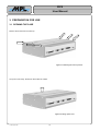
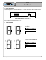
PACKED INDUSTRIAL PC WITH AMD ÉlanTMSC520 PROCESSOR (5x86)
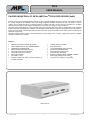
The PIP 5 is a highly integrated robust industrial PC with a special designed aluminum housing. This allows to operate
the system without fan or ventilation holes. The design integrates standard connectors for easy connection. It can be
used for any PC application where a complete solution is needed. The PIP 5 can be used in a standard or in a rugged
operating environment, is 100% PC/AT compatible and can easily be mounted on a 35mm DIN rail.
The PIP housing offers space for a 2,5” hard disk and a slim line floppy disk drive. With the integrated PC/104+ interface
flexible expansion possibilities are available. Fully bootable FLASH disks are supported for projects where hard disks or
floppy cannot be used. Particular special precautions have been taken of the EMC for the entire system to fulfill the CE
and FCC requirements.
All these features make the PIP5 to the ideal solution for the industry where a flexible, rugged and long term available
complete Industrial PC is needed.
Features
•
•
•
•
•
•
•
•
•
•
•
•
•
•
•
•
•
•
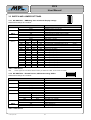
AMD ÉlanTMSC520 Processor @ 133MHz
168pin DIMM socket for up to 256MB SDRAM
Updateable Flash BIOS ROM
RTC and Setup with battery backup
PC/104 and PC/104 Plus interface
10/100 Mbps Ethernet controller
SCSI-2 host adapter
Two USB 1.1 ports
Graphics interface for CRT and Panel Support up
to SXGA resolution
Isolated CAN bus interface
Four RS232 ports
Two isolated RS485 ports (optional)
Parallel port (SPP/EPP/ECP)
PS/2 keyboard & mouse ports
Programmable watchdogs
Socket for additional Flash, EPROM or SRAM
Wide supply voltage range 8-28 VDC
Low power consumption, 7W typically
PIP5-1 Rev.A
2001 by MPL AG
1
MEH-10064-001 Rev. J
PIP5
User Manual
High-Tech • Made in Switzerland
TABLE OF CONTENTS
1. INTRODUCTION ........................................................................................................... 6
1.1
ABOUT THIS MANUAL.............................................................................................................................6
1.2
SAFETY PRECAUTIONS AND HANDLING............................................................................................6
1.3
ELECTROSTATIC DISCHARGE (ESD) PROTECTION ........................................................................6
1.4
EQUIPMENT SAFETY ...............................................................................................................................6
2. GENERAL INFORMATION AND SPECIFICATIONS ................................................... 7
2.1
PRODUCT DESCRIPTION ........................................................................................................................7
2.2
SPECIFICATIONS ......................................................................................................................................8
2.2.1
ELECTRICAL ........................................................................................................................................8
2.2.2
PHYSICAL/POWER.............................................................................................................................11
2.2.3
ENVIRONMENT..................................................................................................................................11
2.3
STANDARDS COMPLIANCE..................................................................................................................12
2.3.1
EMC .....................................................................................................................................................12
2.3.2
ENVIRONMENTAL.............................................................................................................................12
2.3.3
SAFETY ...............................................................................................................................................12
2.3.4
TYPE APPROVAL ...............................................................................................................................12
DIMENSIONS .........................................................................................................................................................13
2.4.1
TOP VIEW ...........................................................................................................................................13
2.4.2
BOTTOM VIEW...................................................................................................................................14
2.4.3
SIDE VIEW 1 .......................................................................................................................................15
2.4.4
SIDE VIEW 2 .......................................................................................................................................16
2.4.5
SIDE VIEW 3 .......................................................................................................................................17
2.4.6
SIDE VIEW 4 .......................................................................................................................................17
2.5
DIFFERENCES TO PREVIOUS REVISIONS.........................................................................................18
2.5.1
CHANGES............................................................................................................................................18
2.5.2
NEW FEATURES.................................................................................................................................18
3. PREPARATION FOR USE.......................................................................................... 19
3.1
OPENING THE CASE...............................................................................................................................19
3.2
PARTS LOCATION ..................................................................................................................................20
3.3
SWITCH AND JUMPER SETTINGS.......................................................................................................21
3.3.1
DIP SWITCH 1 – AMDebug, User switches & Display settings.............................................................21
3.3.2
DIP SWITCH 2 – Disable Devices, MPS mode setting & Misc. .............................................................21
3.3.3
DIP SWITCH 3 - USB port 1 routing.....................................................................................................22
3.3.4
DIP SWITCH 4 - MPS PIN SELECT ....................................................................................................22
3.3.5
JUMPER 1 – POWER UP BEHAVIOR select .......................................................................................22
3.3.6
JUMPER 2 & 3 – RS485 termination select ...........................................................................................22
3.3.7
JUMPER 4 – JTAG CHAIN SELECT ...................................................................................................23
2001 by MPL AG
2
MEH-10064-001 Rev. I
PIP5
User Manual
High-Tech • Made in Switzerland
3.4
EXTERNAL CONNECTORS ...................................................................................................................24
3.4.1
POWER CONNECTOR ........................................................................................................................24
3.4.1.1
MOUNTING AN EXTERNAL RESET- AND POWER BUTTON...................................................24
3.4.2
PARALLEL PORT CONNECTOR .......................................................................................................25
3.4.3
SERIAL-1 AND SERIAL-3 CONNECTOR ..........................................................................................27
3.4.4
SERIAL 2&4 CONNECTOR ................................................................................................................27
3.4.5
CAN CONNECTOR .............................................................................................................................28
3.4.6
SCSI CONNECTOR .............................................................................................................................28
3.4.7
10/100 BASE T/TX CONNECTOR.......................................................................................................29
3.4.8
KEYBOARD AND MOUSE CONNECTOR.........................................................................................29
3.4.9
USB CONNECTOR..............................................................................................................................29
3.4.10
CRT CONNECTOR...........................................................................................................................30
3.5
INTERNAL CONNECTORS.....................................................................................................................31
3.5.1
IDE CONNECTORS.............................................................................................................................31
3.5.1.1
STANDARD IDE CONNECTOR ....................................................................................................31
3.5.1.2
CONNECTOR FOR INTERNAL HDD............................................................................................31
3.5.2
FDD CONNECTOR..............................................................................................................................32
3.5.3
REMOTE MMI AND PANEL MODULE CONNECTOR .....................................................................33
3.5.4
ZOOMED VIDEO PORT CONNECTOR..............................................................................................34
3.5.4.1
SYNCHRONOUS SERIAL INTERFACE SSI (PIN 39/40) ..............................................................34
3.5.5
INTERNAL POWER CONNECTOR ....................................................................................................35
3.5.6
SPEAKER CONNECTOR.....................................................................................................................35
3.5.7
COM4 CONNECTOR...........................................................................................................................35
3.5.8
TIMER INTERFACE CONNECTOR....................................................................................................36
3.5.9
LED CONNECTOR..............................................................................................................................36
3.5.10
PC/104 INTERFACE CONNECTOR.................................................................................................37
3.5.11
PC/104 PLUS INTERFACE Connector..............................................................................................38
3.5.12
AMDebug / JTAG CONNECTOR .....................................................................................................39
3.6
CABLE REQUIRE MENTS ......................................................................................................................39
3.7
MODULE SOCKETS ................................................................................................................................40
3.7.1
SDRAM MEMORY MODULE SOCKET .............................................................................................40
3.7.1.1
MOUNTING THE MEMORY MODULE ........................................................................................40
3.7.2
RS485/RS422 INTERFACE MODULE SOCKETS ...............................................................................41
3.7.2.1
MOUNTING THE MODULES ........................................................................................................41
3.7.2.2
TERMINATION JUMPERS ............................................................................................................41
3.7.3
MULTI PURPOSE SOCKET (MPS) .....................................................................................................42
3.7.3.1
MPS USED FOR MEMORY MODULES ........................................................................................42
3.7.3.2
REQUIRED MODULE PROPERTIES.............................................................................................42
3.7.3.3
MANUFACTURERS OF MEMORY COMPONENTS FOR MPS ...................................................42
3.7.3.4
PIN CONFIGURATION..................................................................................................................43
3.7.3.5
MEMORY MODULE SETUP .........................................................................................................44
3.8
REMOTE MMI AND PANNEL MODULE SOCKET .............................................................................45
3.8.1
EASY PANEL AND MAN MACHINE INTERFACE (MMI) SUPPORT ..............................................45
3.8.2
MOUNTING A PANEL OR MMI MODULE........................................................................................46
4. OPERATION ............................................................................................................... 47
BLOCK DIAGRAM ................................................................................................................................................47
4.2
PC/AT FUNCTIONALITY........................................................................................................................48
4.3
STATUS INDICATORS ............................................................................................................................48
4.3.1
POWER INDICATOR LED ..................................................................................................................48
2001 by MPL AG
3
MEH-10064-001 Rev. I
PIP5
User Manual
High-Tech • Made in Switzerland
4.3.2
4.3.3
4.3.4
4.3.5
4.3.6
4.3.7
4.4
RESET INDICATOR LED....................................................................................................................48
HDD ACCESS INDICATOR LED........................................................................................................48
SCSI ACCESS INDICATOR LED ........................................................................................................48
LAN INDICATOR LED........................................................................................................................48
LAN100 INDICATOR LED..................................................................................................................48
USER1, USER2 INDICATOR LED’s....................................................................................................48
BATTERY CIRCUIT.................................................................................................................................48
4.5
PROGRAMMABLE WATCHDOG TIMERS ..........................................................................................49
4.5.1
ÉLANTMSC520 WATCHDOG ..............................................................................................................49
4.5.1.1
PROGRAMMING THE ELAN WATCHDOG.................................................................................49
4.5.2
SUPER I/O WATCHDOG.....................................................................................................................49
4.5.2.1
PROGRAMMING THE SIO WATCHDOG.....................................................................................49
4.6
SOFTWARE TIMER.................................................................................................................................50
4.6.1
USING THE SOFTWARE TIMER .......................................................................................................50
4.7
RS-485 / RS422 INTERFACES (OPTIONAL)..........................................................................................51
4.7.1
HALF DUPLEX TRANSMITTER CONTROL .....................................................................................51
4.7.2
FULL DUPLEX MODE ........................................................................................................................51
4.7.3
HIGH SPEED MODE ...........................................................................................................................51
4.8
CAN INTERFACE.....................................................................................................................................52
4.9
USING PC/AT INTERRUPTS...................................................................................................................53
4.10
USING PC/AT DMA CHANNELS ........................................................................................................54
4.11
EXTENSION REGISTERS....................................................................................................................55
4.11.1
RESERVED ......................................................................................................................................55
4.11.2
DMA CHANNEL 1/0 MAPPING ......................................................................................................55
4.11.3
DMA CHANNEL 3/2 MAPPING ......................................................................................................55
4.11.4
PIP5 MISCELLANEOUS ..................................................................................................................56
4.11.5
CAN RESOURCE MAPPING ...........................................................................................................57
4.11.6
CAN CONTROL ...............................................................................................................................58
4.11.7
MPS PAGE CONTROL.....................................................................................................................58
4.11.8
MPS PAGE ADDRESS .....................................................................................................................59
4.11.9
SIO WATCHDOG CONTROL ..........................................................................................................59
4.11.10
USER LED CONTROL .....................................................................................................................60
4.11.11
STATUS CONFIGURATION SWITCHES........................................................................................60
4.11.12
STATUS USER SWITCHES .............................................................................................................61
4.11.13
RS485/232 CONTROL ......................................................................................................................62
4.11.14
PIP FAMILY IDENTIFICATION......................................................................................................63
4.11.15
PLD04 IDENTIFICATION................................................................................................................63
4.11.16
PLD05 IDENTIFICATION................................................................................................................63
4.12
EMC FEATURES...................................................................................................................................64
5. PERFORMANCE......................................................................................................... 65
5.1
1st LEVEL CACHE ....................................................................................................................................65
5.1.1
CACHEABLE AREA ...........................................................................................................................65
5.2
HDD PERFORMANCE.............................................................................................................................65
2001 by MPL AG
4
MEH-10064-001 Rev. I
PIP5
User Manual
High-Tech • Made in Switzerland
6. SOFTWARE ................................................................................................................ 66
6.1
BIOS ...........................................................................................................................................................66
6.1.1
BIOS UPDATE .....................................................................................................................................66
6.1.2
BIOS RELEASE INDEX ......................................................................................................................66
6.1.3
BIOS SETUP SCREEN - Custom Configuration....................................................................................67
6.1.3.1
PARALLEL PORT FLOPPY SETTINGS ........................................................................................67
6.1.3.2
CAN CONTROLLER SETTINGS ...................................................................................................67
6.1.3.3
RS485 / RS422 SETTINGS..............................................................................................................68
6.1.3.4
COM2 SPEED SETTING ................................................................................................................68
6.1.3.5
IR MODE SETTING .......................................................................................................................68
6.1.3.6
MPS SETTINGS..............................................................................................................................69
6.1.3.7
SETTING UP A MEMORY WINDOW FOR PC104........................................................................70
6.2
DEVICE DRIVERS....................................................................................................................................71
7. SUPPORT INFORMATION ......................................................................................... 72
7.1
MPL AG .....................................................................................................................................................72
7.2
PRODUCTION REVISION NUMBER.....................................................................................................72
7.3
RELATED DOCUMENTS ........................................................................................................................72
7.4
DOCUMENT REVISION HISTORY........................................................................................................72
2001 by MPL AG
5
MEH-10064-001 Rev. I
PIP5
User Manual
High-Tech • Made in Switzerland
1. INTRODUCTION
1.1 ABOUT THIS MANUAL
This manual assists the installation and initialization procedure by providing all the information necessary to handle and
configure the PIP5.
The manual is written for technical personnel responsible for integrating the PIP5 into their system.
1.2 SAFETY PRECAUTIONS AND HANDLING
For personal safety and safe operation of the PIP5, follow all safety procedures described here and in other sections of
the manual.
•
•
•
Power must be removed from the system before installing (or removing) the PIP5 to prevent the possibility of
personal injury (electrical shock) and/or damage to the product.
Handle the product carefully, i.e. dropping or mishandling the PIP5 can cause damage to assemblies and
components.
Do not expose the equipment to moisture.
WARNING
There are no user-serviceable components on the PIP5 except the battery!
1.3 ELECTROSTATIC DISCHARGE (ESD) PROTECTION
Various electrical components within the product are sensitive to static and electrostatic discharge (ESD). Even a nonsensible static discharge can be sufficient to destroy or degrade a component's operation!
With an open housing, do not touch any electronic components. Handle or touch only the unit chassis.
1.4 EQUIPMENT SAFETY
Great care is taken by MPL that all its products are thoroughly and rigorously tested before leaving the factory to ensure
that they are fully operational and conform to specification. However, no matter how reliable a product, there is always
the remote possibility that a defect may occur. The occurrence of a defect on this device may, under certain conditions,
cause a defect to occur in adjoining and/or connected equipment. It is the user’s responsibility to ensure that adequate
protection for such equipment is incorporated when installing this device. MPL accepts no responsibility whatsoever for
such kind of defects, however caused.
2001 by MPL AG
6
MEH-10064-001 Rev. I
PIP5
User Manual
High-Tech • Made in Switzerland
2. GENERAL INFORMATION AND SPECIFICATIONS
This section provides a general overview over the PIP5 and its features. It outlines the electrical and physical
specifications of the product and its power requirements.
2.1 PRODUCT DESCRIPTION
CPU AMD ÉlanTMSC520-133MHz
The ÉlanTMSC520 microcontroller combines a 32-bit, low-voltage Am5x86 CPU with a complete set of integrated
peripherals suitable for both real-time and PC/AT-compatible embedded applications. It has a 16-Kbyte write-back or
write-through cache, Floating Point Unit (FPU), Integrated PC/AT peripherals and a Synchronous Serial Interface (SSI).
The device also features a 32-bit PCI bus, a high-performance, 32-bit SDRAM interface and a full-featured, highperformance incircuit emulation capability, known as the AMDebug™ utility.
The instruction set includes the complete 486 microprocessor instructions and is compatible to every member of the x86
family. Because of the processor operating frequency of 133MHz, system performance increases over a Pentium P75,
while maintaining complete compatibility with the standard 486 processor architecture.
Memory
The PIP5 is equipped with one standard 168-pin DIMM socket for an SDRAM Module.
SDRAM
One SDRAM DIMM module can house up to 256 Mbytes.
Storage
An internal 2,5“ hard disk and a slim line floppy disk drive can be connected to E-IDE and FDD interfaces. The local-bus
E-IDE interface supports all ANSI standard devices using PIO modes 0,1 and 2 (two devices in master/slave
configuration on each IDE channel are supported). The FDD port allows operation up to 2.88 Mbytes.
PC/104 /Plus interface
The PIP5 is a true single board computer with all PC/AT features on board and therefore the use of a backplane is not
required. Nevertheless the standard PC/104 and PC/104 Plus interfaces allow flexible extension with additional
peripherals.
Software
The PIP5 is set up with the General Software BIOS. Any operating system for a PC/AT can be run on the PIP5.
2001 by MPL AG
7
MEH-10064-001 Rev. I
PIP5
User Manual
High-Tech • Made in Switzerland
2.2 SPECIFICATIONS
2.2.1 ELECTRICAL
Processor:
•
AMD ÉlanTMSC520, industry-standard Am5x86 CPU
•
Floating Point Unit (FPU)
•
32-Bit data bus
•
16 Kbytes write-back or write-through cache
•
100 or 133 MHz operating frequency
•
Integrated PCI host bridge controller
•
Synchronous DRAM (SDRAM) controller
•
Enhanced DMA controller
•
Enhanced programmable interrupt controller (PIC)
•
Programmable interval timer (PIT)
•
Real-time clock (RTC)
•
Two serial ports
Super IO:
•
Floppy disk controller
•
PS/2 Keyboard and Mouse controller
•
IEEE1248 compliant parallel port (SPP/EPP/ECP)
•
Two serial ports, optional infrared interface on UART2
BIOS ROM:
•
256kB Flash EEPROM (256k x 8; 128 Bytes per page, 2048 pages)
•
easy BIOS update
RTC and CMOS Setup:
•
Backed with on field changeable onboard battery
Memory:
•
Socket for one 168 pin DIMM memory module
•
Up to 256 Mbytes (1 module)
•
3.3VDC 66 MHz SDRAM or faster can be used
•
Supports 16-, 64-, 128- and 256Mbit SDRAM technology
•
64-bit data bus
•
Error Correction Code (ECC) is not supported
Multi Purpose Socket:
•
Supports different SRAM/FLASH/EPROM, 28 and 32 pin DIL memory devices
•
Memory sizes up to 512kB
•
Selectable memory windows
PC/104 /Plus interface:
•
16 Bit PC/104 interface (up to 2 slots), external bus master not supported
•
32 Bit PC/104 Plus interface (up to 2 slots)
Serial RS232 ports:
•
Four serial RS232 ports, configured as COM1 ... COM4
•
16C550 compatible (16Byte FIFO)
•
Transfer rates on all RS-232 ports up to 115.2 kBaud
•
On COM1 to COM3 all modem signals are available
•
Optionally 2 ports can be equipped with RS485/RS422 interface modules
•
Optionally COM4 can also be used as full modem interface
•
Available on two standard DB9 and one DB25 connector
•
ESD protected
2001 by MPL AG
8
MEH-10064-001 Rev. I
PIP5
User Manual
High-Tech • Made in Switzerland
RS485/RS422 interface modules (optional):
•
Electrically fully isolated
•
Half duplex (2-wire) operation
•
2 modules can be switched together for one full duplex (4-wire) port
•
Transfer rates up to 1.152 Mbaud on COM2
•
Available on DB25 connector
•
ESD protected
Infrared port:
•
COM4 can be used optionally as infrared port
•
ASK-IR and IrDA mode
•
Transfer rates up to 4 Mbaud (Fast Ir)
•
Available on DB25 connector
•
ESD protected
Parallel port:
•
IEEE1284 compliant
•
SPP, EPP1.7, EPP1.9, ECP mode support
•
Configurable as LPT1, LPT2, LPT3
•
Floppy Disk on parallel port mode
•
Available on DB25 connector
•
ESD protected
E-IDE ports:
•
2 separate channels for up to 4 drives
•
44 pin header (internal), 2 mm pitch, for internal 2,5” Notebook hard disk (primary IDE)
•
40-pin header (internal), 2.54 mm (0.1'') pitch for service and installation purposes (secondary IDE)
•
PIO Mode 0, 1 and 2
•
Activity indicator on case cover
Floppy disk:
•
Up to 2.88 Mbytes FDD supported
•
26-pin flex cable connector used for internal slim line floppy disk
•
Signals can also be routed to parallel port connector (if external floppy is needed)
CAN bus:
•
Intel AN82527 CAN controller
•
Supports CAN specification 2.0
•
Opto isolated with external supply 9V ... 28Vdc, 100mA max.
•
Power input reverse polarity protected
•
ISO/DIS 11898, high speed (1 Mbit/sec)
•
Input + output delay 270ns max.
•
Available on a DB-9 connector(CiA DS102-1)
•
Device drivers for DOS, Windows 3.11 and Windows 9x available
•
ESD protected
Graphic:
•
Chips & Technology 69000 Graphics Accelerator with 64 bit graphic engine
•
2 Mbytes video memory
•
Resolutions up to 1280x1024 pixels (SXGA)
•
Colors up to 64k
•
Refresh-rates up to 85 Hz
•
DPMS and DDC support
•
Simultaneous CRT and panel operation
•
Standard D-Sub 15HD CRT connector
•
MPL Remote MMI module (REMMI)
•
Flexible panel support for TFT and STN panels, resolutions up to 1280x1024 (SXGA)
•
Hardware chip disable function
2001 by MPL AG
9
MEH-10064-001 Rev. I
PIP5
User Manual
High-Tech • Made in Switzerland
Ethernet:
•
Intel 82559ER Fast 10/100 Mbps Ethernet Controller
•
Full 32-bit PCI bus master
•
IEEE802.3 10BASE-T and 100BASE-TX compatible
•
IEEE 802.3u Autonegotiation Support
•
Hardware chip disable function
•
Activity indicators for link detection/network traffic and 100 Mbit/s operation
on case cover and connector
•
Device drivers for all major operation systems available
•
ESD protected
SCSI:
•
LSI Logic (Symbios) SYM53C810A Fast SCSI-2 Host Controller
•
Full 32-bit PCI bus master
•
Not bootable
•
ASPI, SCAM and Fast SCSI-2 compatible
•
Up to 7 Mbytes/s asynchronous and 10 Mbytes/s synchronous transfer rate
•
Available on a 50 pin SCSI-2 connector
•
Hardware chip disable function
•
Device drivers for all major operation systems available
•
Activity indicator on case cover
•
ESD protected
USB:
•
CMD 673 PCI to USB host controller
•
Full 32-bit PCI bus master
•
Two USB 1.1 ports for serial transfers up to 12 Mbit/s
•
Hardware chip disable function
•
ESD protected
Keyboard / Mouse:
•
Available on 6-pin mini DIN connectors (PS/2)
•
ESD protected
Speaker:
•
Available on a internal 4-pin header
Watchdog Timers:
•
One watchdog with a timeout duration configurable between 1...255 seconds or 1...255 minutes
•
One programmable watchdog timer with distinct keyed write sequence and a timeout duration configurable between
0.5msec .. 32sec
Miscellaneous:
•
Software timer provide a millisecond timebase with microsecond resolution (max. 65.5sec)
Reset-, Powerbutton:
•
Reset button, protected against unintended actuation
•
Connection for an external remote reset button
•
Connection for an external remote power button
Indicators:
•
Power LED (yellow)
•
Reset / Power Fail LED (red)
•
HDD activity LED (green)
•
SCSI activity LED (green)
•
LAN link/activity LED (green)
•
LAN 100Mbps LED (green)
•
2 user programmable LED’s (green)
2001 by MPL AG
10
MEH-10064-001 Rev. I
PIP5
User Manual
High-Tech • Made in Switzerland
2.2.2 PHYSICAL/POWER
Housing:
•
Aluminum
•
No ventilation wholes
•
Easy mountable on 35mm DIN rail
Form factor:
Length: 270 mm (6,86’’)
Width: 162 mm (4,12’’)
Height: 62 mm (1,57’’) small version (standard)
83 mm (2,10’’) medium version
120mm (3,05’’) high version
Weight:
Typical ca. 2,2kg (4,85 lbs.)
(Standard housing version, equipped with internal 2,5’’ HDD and FDD)
Power supply:
Dual high efficiency switching regulator
ESD protected
Fuse:
5x20mm, 3,15AT
Battery:
Lithium Coin Cell CR2032 (20.0 x 3.2 mm)
3 V / 235 mAh
Field changeable
Input Power Range:
+8V...+28VDC
Power consumption:
+12V: 0.58A typ. @ 133 MHz (operating with 64 MB SDRAM, internal 2,5’’ HDD and FDD)
2.2.3 ENVIRONMENT
Temperature range:
Operational:
Standard range: -20°C to +60°C @ 133 MHz CPU speed without heat sink
Extended range: -40°C to +75°C @ 133 MHz CPU speed without heat sink
Storage:
Standard range: -45°C to +85°C
Relative humidity:
5% to 95% RH non condensing
2001 by MPL AG
11
MEH-10064-001 Rev. I
PIP5
User Manual
High-Tech • Made in Switzerland
2.3 STANDARDS COMPLIANCE
The PIP5 is designed to meet or exceed the most common industry and military standards. Particular references are:
2.3.1 EMC
•
•
•
•
•
•
•
•
•
•
•
•
•
EN 55022 Class B (Information technology equipment - Radio disturbance characteristics - Limits and methods of
measurement)
EN 55024 (Information technology equipment - Immunity characteristics - Limits and methods of measurement)
EN 61000-4-1 (Electromagnetic compatibility (EMC) -- Part 4-1: Testing and measurement techniques - Overview of
IEC 61000-4 series)
EN 61000-4-2 Level 3, Criterion B (Electromagnetic compatibility (EMC) -- Part 4-2: Testing and measurement
techniques - Electrostatic discharge immunity test)
EN 61000-4-3 Level 3, Criterion A (Electromagnetic compatibility (EMC) -- Part 4-3: Testing and measurement
techniques - Radiated, radio-frequency, electromagnetic field immunity test)
EN 61000-4-4 Class 3 (Electromagnetic compatibility (EMC) -- Part 4-4: Testing and measurement techniques Electrical fast transient/burst immunity test)
EN 61000-4-5 Class 3 (Electromagnetic compatibility (EMC) -- Part 4-5: Testing and measurement techniques Surge immunity test)
EN 61000-4-6 Class 3 (Electromagnetic compatibility (EMC) -- Part 4-6: Testing and measurement techniques Immunity to conducted disturbances, induced by radio-frequency fields)
EN 61000-6-1 (Electromagnetic compatibility (EMC) -- Part 6-1: Generic standards - Immunity for residential,
commercial and light-industrial environments)
EN 61000-6-2 (Electromagnetic compatibility (EMC) -- Part 6-2: Generic standards - Immunity for industrial
environments)
EN 61000-6-3 (Electromagnetic compatibility (EMC) -- Part 6-3: Generic standards - Emission standard for
residential, commercial and light-industrial environments)
EN 61000-6-4 (Electromagnetic compatibility (EMC) -- Part 6-4: Generic standards - Emission standard for industrial
environments)
MIL-STD-461E (REQUIREMENTS FOR THE CONTROL OF ELECTROMAGNETIC INTERFERENCE
CHARACTERISTICS OF SUBSYSTEMS AND EQUIPMENT)
2.3.2 ENVIRONMENTAL
•
•
EN 50155 (Railway applications - Electronic equipment used on rolling stock)
MIL-STD-810-F (ENVIRONMENTAL ENGINEERING CONSIDERATIONS AND LABORATORY TESTS)
2.3.3 SAFETY
•
•
EN 60601-1 (Medical electrical equipment -- Part 1: General requirements for safety)
EN 60950 Class III (Information technology equipment - Safety)
2.3.4 TYPE APPROVAL
•
•
EN 60945 Protected Equipment (Maritime navigation and radiocommunication equipment and systems - General
requirements - Methods of testing and required test results)
IACS E10 ( Test Specification for Type Approval)
2001 by MPL AG
12
MEH-10064-001 Rev. I
PIP5
User Manual
High-Tech • Made in Switzerland
2.4 DIMENSIONS
SIDE VIEW 1
32,5
40,1
47,7
55,4
63,0
70,6
78,2
85,8
270,0
106,2
SIDE VIEW 2
SIDE VIEW 3
2.4.1 TOP VIEW
162,1
48,3
SIDE VIEW 4
Note:
All dimensions are subject to be changed.
2001 by MPL AG
13
MEH-10064-001 Rev. I
PIP5
User Manual
High-Tech • Made in Switzerland
2.4.2 BOTTOM VIEW
270,0
185,0
165,0
105,0
85,0
SIDE VIEW 2
SIDE VIEW 1
SIDE VIEW 4
109,5
81,1
59,5
SIDE VIEW 3
162,1
Note:
All dimensions are subject to be changed.
2001 by MPL AG
14
MEH-10064-001 Rev. I
PIP5
User Manual
High-Tech • Made in Switzerland
2.4.3 SIDE VIEW 1
SIDE VIEW 3
(49,4 / 53,9)
(56,9 / 61,4)
(64,4 / 68,9)
(45,9 / 50,4)
DSUB-25
BOTTOM VIEW
64,
7
81,
8
85,
0
106,
8
122,
5
147,
5
165,
3
185,
0
212,
3
229,
6
254,
6
270,
0
DSUB-25
17,
7
21,
2
251,
1
221,
0
168,
9
165,
4
106,
9
103,
4
73,
3
82,3 x 15
DSUB-9
DSUB-9
TOP VIEW
8,5
82,3 x 15
DSUB-9
29,
9
33,
4
40,
9
48,
4
62,
0
24,
3
SIDE VIEW 4
(82,5 / 120,0)
Note:
Numbers in brackets are to be used for the high versions (82.5mm or 120mm).
All dimensions are subject to be changed.
2001 by MPL AG
15
MEH-10064-001 Rev. I
PIP5
User Manual
High-Tech • Made in Switzerland
2.4.4 SIDE VIEW 2
21,
0
37,
9
SIDE VIEW 4
24,
5
8,5
TOP VIEW
BOTTOM VIEW
23,
4
24,
5
22,
1
270,
0
160,
7
127,
4
119,
5
23,
3
23,
2
52,
1
76,
5
85,
0
101,
5
120,
8
167,
2
185,
0
190,
6
208,
2
232,
1
252,
1
270,
0
30,
7
24,
8
SIDE VIEW 3
62,
0
24.
0
(82,5 / 120,0)
Note:
Numbers in brackets are to be used for the high versions (82.5mm or 120mm).
All dimensions are subject to be changed.
2001 by MPL AG
16
MEH-10064-001 Rev. I
PIP5
User Manual
High-Tech • Made in Switzerland
2.4.5 SIDE VIEW 3
144,
9
110,
9
67,
7
43,
0
TOP VIEW
SIDE VIEW 2
SIDE VIEW 1
8,5
4
33.
4
4,6
62,
0
46.
(82,5 / 120,0)
4.6
17,
2
59.
5
94,
4
109.
5
162,
1
BOTTOM VIEW
2.4.6 SIDE VIEW 4
144,
9
94,
4
TOP VIEW
SIDE VIEW 1
SIDE VIEW 2
52.
5
67,
7
102.
5
107,
5
162,
1
Note:
8,5
35,
4
4,6
62,
0
(82,5 / 120,0)
4.6
17,
2
BOTTOM VIEW
Numbers in brackets are to be used for the high versions (82.5mm or 120mm).
All dimensions are subject to be changed.
2001 by MPL AG
17
MEH-10064-001 Rev. I
PIP5
User Manual
High-Tech • Made in Switzerland
2.5 DIFFERENCES TO PREVIOUS REVISIONS
Between the former PIP5 revisions A to C and revision D, or above, some major changes have been made. This also
means, that this manual can NOT be used for the former PIP5 revisions.
This section is thought particularly for users of devices of the former revisions and shall show the differences which are
important at exchange, etc. Please contact your local distributor or MPL AG for further information about the changes.
2.5.1 CHANGES
•
•
•
•
•
•
•
•
•
•
•
New CPU-, Graphic-, Ethernet- and SCSI-chip on board
Placement of connectors changed
10Base-2 port removed
34 pin internal FDD connector removed
72 pin SO-DIMM sockets for flash removed
Pinning of Serial 2+4 connector changed
(Modem signals of COM4 were removed. These pins are used for IrDA signals instead.)
168 pin DIMM socket for SDRAM memory instead of 72 pin SO-DIMM sockets for DRAM
New panel and MMI interface implemented
New watchdog timers
DIP-Switch settings have been changed (new functionality)
Extension Registers have been changed (new functionality)
2.5.2 NEW FEATURES
•
•
•
•
•
•
•
Two USB ports
PC/104 Plus interface
“Multi Purpose Socket” for different memory devices (SRAM/FLASH/EPROM)
Now two separate IDE channels for up to four drives available
Infrared interface possibility
ZV port interface
Selectable power up behavior
2001 by MPL AG
18
MEH-10064-001 Rev. I
PIP5
User Manual
High-Tech • Made in Switzerland
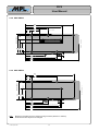
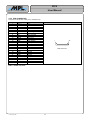
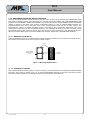
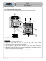
3. PREPARATION FOR USE
3.1 OPENING THE CASE
Remove the screws from the case top.
Figure 3-1 Removing the case top screws
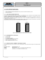
Lift up the cover slowly. Please be careful with the cables.
Figure 3-2 Lifting up the cover
2001 by MPL AG
19
MEH-10064-001 Rev. I
PIP5
User Manual
High-Tech • Made in Switzerland
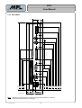
3.2 PARTS LOCATION
Figure 3-3 Parts Location
2001 by MPL AG
20
MEH-10064-001 Rev. I
PIP5
User Manual
High-Tech • Made in Switzerland
1
2
3
4
5
6
7
8
3.3 SWITCH AND JUMPER SETTINGS
3.3.1 DIP SWITCH 1 – AMDebug, User switches & Display settings
Default switch settings are in brackets.
Switch S1
SW1-1
ON
(OFF)
ON
(OFF)
ON
(OFF)
ON
(OFF)
(ON)
(ON)
ON
ON
OFF
ON
OFF
ON
ON
OFF
ON
OFF
OFF
OFF
OFF
OFF
ON
ON
ON
ON
OFF
ON
OFF
ON
ON
OFF
ON
OFF
OFF
OFF
OFF
OFF
SW1-2
SW1-3
SW1-4
SW1-5...8
(Note 1)
(ON)
OFF
ON
OFF
ON
OFF
ON
OFF
ON
OFF
ON
OFF
ON
OFF
ON
OFF
(ON)
ON
ON
ON
ON
ON
ON
ON
OFF
OFF
OFF
OFF
OFF
OFF
OFF
OFF
Meaning
AMDebug Enter is turned on
AMDebug Enter is turned off
AMDebug Instruction Trace is turned on
AMDebug Instruction Trace is turned off
Serial Console On (Kb & VGA to COM1)
Serial Console Off
User switch 1 is low
User switch 1 is high
TFT Panel with 640x480 pixels, 24 bit
TFT Panel with 800x600 pixels, 24 bit
TFT Panel with 1024x768 pixels, 24 bit
TFT Panel with 1280x1024 pixels, 24 bit
TFT Panel with 320x240 pixels, 24 bit
Panel Type #5 (TBD)
Panel Type #6 (TBD)
Panel Type #7 (TBD)
Panel Type #8 (TBD)
Panel Type #9 (TBD)
Panel Type #10 (TBD)
Panel Type #11 (TBD)
Panel Type #12 (TBD)
Panel Type #13 (TBD)
Panel Type #14 (TBD)
Panel Type #15 (TBD)
O
N
(VGA)
(SVGA)
(XGA)
(SXGA)
(QVGA)
Table 3-1 DIP Switch 1
1. Panel Types are to be defined. Please contact your distributor or MPL AG for further information.
O
N
Note:
1
2
3
4
5
6
7
8
3.3.2 DIP SWITCH 2 – Disable Devices, MPS mode setting & Misc.
Default switch settings are in brackets.
Switch S2
SW2-1
ON
(OFF)
ON
(OFF)
ON
(OFF)
ON
(OFF)
SW2-2
SW2-3
SW2-4
SW2-5..6
SW2-7
SW2-8
(ON)
OFF
ON
OFF
(ON)
ON
OFF
OFF
ON
(OFF)
ON
(OFF)
Meaning
On board VGA controller disabled
On board VGA controller enabled
On board Ethernet controller disabled
On board Ethernet controller enabled
On board USB controller disabled
On board USB controller enabled
On board SCSI controller disabled
On board SCSI controller enabled
MPS disabled
MPS device is a Flash
MPS device is an EPROM
MPS device is a SRAM
PIP5 boots from device on Multi-Purpose socket
PIP5 boots from on board flash
Battery backup on
Battery backup off
Table 3-2 DIP Switch 2
2001 by MPL AG
21
MEH-10064-001 Rev. I
PIP5
User Manual
High-Tech • Made in Switzerland
3.3.3 DIP SWITCH 3 - USB port 1 routing
This switch determines whether the USB port 1 signals are routed to the external USB port 1 connector (J19) or to the
internal Remote MMI module connector (J16).
USB port 1 signals are routed to USB port 1 connector (J19) - default.
USB Port 1 signals are routed to Remote MMI module connector (J16).
3.3.4 DIP SWITCH 4 - MPS PIN SELECT
This switch determines weather a 28 pin or 32 pin device is placed in the Multi-Purpose Socket.
32 pin device mounted on Multi-Purpose Socket.
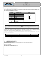
28 pin device mounted on Multi-Purpose Socket.
3.3.5 JUMPER 1 – POWER UP BEHAVIOR select
Through this jumper the power up behavior of the PIP5 can be selected.
1
3
2
4
1
3
2
4
PIP5 starts up automatic if power is turned on – default.
After power is turned on the PIP5 waits with start up until the power button is pushed.
3.3.6 JUMPER 2 & 3 – RS485 termination select
With this jumpers the termination and as option a dominant level of the RS485 lines can be selected.
1
2
5
6
1
2
5
6
Standard 120 Ω termination between RS485 lines – default.
Open RS485 lines without termination.
If a termination with dominant recessive levels on the RS485 lines is necessary please contact MPL for further details.
2001 by MPL AG
22
MEH-10064-001 Rev. I
PIP5
User Manual
High-Tech • Made in Switzerland
3.3.7 JUMPER 4 – JTAG CHAIN SELECT
With this jumpers the JTAG chain order can be selected. Following devices can be in the chain: EPLD1, EPLD2, EPLD3
and Elan.
1
2
All devices in chain with following order: EPLD1, EPLD2, EPLD3 and Elan.
5
6
1
2
5
6
1
2
5
6
2001 by MPL AG
Only the EPLD’s are in the chain (order: EPLD1, EPLD2, EPLD3).
Only the Elan is in the chain, this setting is used for debugging – default.
23
MEH-10064-001 Rev. I
PIP5
User Manual
High-Tech • Made in Switzerland
3.4 EXTERNAL CONNECTORS
3.4.1 POWER CONNECTOR
Through this connector power for the PIP5 is provided. No other inputs than this must be used to power the PIP5.
4-pin power connector Phoenix Contact AG typ MC1,5/4-GF-3.81 pinout:
Pin number
1
2
3
4
Signal
VIN
GND
RSTBTN
PWRBTN
Description
Input voltage (+8...28 VDC)
Ground
System Reset Input (active low)
Power Button Input (active low)
Pinout
1 2 3 4
Table 3-3 Power connector
Counterpart is the Phoenix Contact AG connector typ MC1,5/4-STF-3.81 (5-10A).
WARNING
Be aware of the input voltage polarization !
Wrong polarization of the input voltage can cause serious damage to the PIP5!
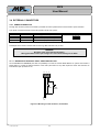
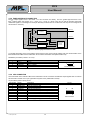
3.4.1.1 MOUNTING AN EXTERNAL RESET- AND POWER BUTTON
On the RSTBTN and PWRBTN pins exist the possibility to mount an external Reset Button for system reset and/or a
Power Button to control the startup behavior of the PIP5 (see section 3.3.5). Both inputs are active low and have an
internal 47kΩ pull up resistor to VIN.
1 2 3 4
Reset
Power
Button
+ VIN
Figure 3-4 Mounting an external Reset-, Powerbutton
2001 by MPL AG
24
MEH-10064-001 Rev. I
PIP5
User Manual
High-Tech • Made in Switzerland
3.4.2 PARALLEL PORT CONNECTOR
The connector for the parallel port is a standard 25 pin female DSUB connector. The parallel port can also operate as
external Floppy Disk Port. The two modes can be switched in the BIOS setup (“Custom Configuration”). If the connector
is used as Floppy Disk Port, pin25 can be used to power the external Floppy (+5V), this can also be selected in the BIOS
setup.
Using the parallel port connector as normal LPT Port:
Pin number
1
2
3
4
5
6
7
8
9
10
11
12
13
14
15
16
17
18
19
20
21
22
23
24
25
Signal
/STRB
DATA0
DATA1
DATA2
DATA3
DATA4
DATA5
DATA6
DATA7
/ACK
BUSY
PE
SEL
/ALF
/ERR
/INIT
/SELIN
GND
GND
GND
GND
GND
GND
GND
GND
LPT mode on parallel port
Description
Strobe
Data bit 0
Data bit 1
Data bit 2
Data bit 3
Data bit 4
Data bit 5
Data bit 6
Data bit 7
Acknowledge
Busy
Paper empty
Select
Auto line feed
Error
Initialize
Select in
Ground
Ground
Ground
Ground
Ground
Ground
Ground
Ground
Pinout
13
1
25
14
DSUB25
Table 3-4 Parallel port connector used in LPT mode
2001 by MPL AG
25
MEH-10064-001 Rev. I
PIP5
User Manual
High-Tech • Made in Switzerland
Using the parallel port connector as Floppy Disk Port:
Pin number
1
2
3
4
5
6
7
8
9
10
11
12
13
14
15
16
17
18
19
20
21
22
23
24
25
Signal
DS0
IDX
TR00
WP
RDATA
DSKCHG
MID0
MTR0
MID1
DS1
MTR1
WDATA
WGATE
DRVDEN0
HDSEL
DIR
STEP
GND
GND
GND
GND
GND
GND
GND
GND or +5V
Floppy Disk Mode on parallel Port
Description
Drive Select 0
Index
Track 0
Write protected
Read Data
Disk Change
Media ID 0
Motor On 0
Media ID 1
Drive Select 1
Motor On 1
Write Data
Write Gate
Drive Density 0
Head Select
Direction
Step
Ground
Ground
Ground
Ground
Ground
Ground
Ground
Selectable in the BIOS
setup (default to GND)
Pinout
13
1
25
14
DSUB25
Table 3-5 Parallel port connector used in Floppy mode
WARNING
Be aware that pin 25 changes power level from GND to +5VDC
if the option “Parallel FDD Power” is enabled in the BIOS setup!
Wrong voltage on pin 25 can cause serious damage to attached peripherals!
2001 by MPL AG
26
MEH-10064-001 Rev. I
PIP5
User Manual
High-Tech • Made in Switzerland
3.4.3 SERIAL-1 AND SERIAL-3 CONNECTOR
The connectors for these serial ports are standard 9 pin male DSUB connector.
Pin number
1
2
3
4
5
6
7
8
9
Signal
/DCD
RXD
TXD
/DTR
GND
/DSR
/RTS
/CTS
/RI
Description
Carrier detect
Receive data
Transmit data
Data terminal ready
Ground
Data set ready
Request to send
Clear to send
Ring indicator
Pinout
1
5
9
6
DSUB9
Table 3-6 Serial-1 and Serial-3 connectors
3.4.4 SERIAL 2&4 CONNECTOR
The connector with this serial ports is a standard 25 pin male DSUB connector.
Pin number
1
2
3
4
5
6
7
8
9
10
11
12
13
14
15
16
17
18
19
20
21
22
23
24
25
Signal
GND
TXD2
RXD2
/RTS2
/CTS2
/DSR2
GND
/DCD2
IRRX3
/CTS4
485B3/4
485B2
485SHLD2
TXD4
IRRX
RXD4
VCC
IRTX
/RTS4
/DTR2
GND
/RI2
485SHLD3/4
485A3/4
485A2
Description
Ground
Transmit data (SERIAL 2)
Receive data (SERIAL 2)
Request to send (SERIAL 2)
Clear to send (SERIAL 2)
Data set ready (SERIAL 2)
Ground
Carrier detect (SERIAL 2)
Control pin for Fast IrDA (TTL level; controlled from UART4)
Clear to send (SERIAL 4)
RS485 balanced RTX3/4- line; RX2- line in full duplex mode
RS485 balanced RTX2- line; TX2- line in full duplex mode
RS485 isolated shield (SERIAL 2)
Transmit data (SERIAL 4)
Infrared Receive signal (TTL level; controlled from UART4)
Receive data (SERIAL 4)
+5VDC
Infrared Transmit signal (TTL level; controlled from UART4)
Request to send (SERIAL 4)
Data terminal ready (SERIAL 2)
Ground
Ring indicator (SERIAL 2)
RS485 isolated shield (SERIAL 3/4)
RS485 balanced RTX3/4+ line; RX2+ line in full duplex mode
RS485 balanced RTX2+ line; TX2+ line in full duplex mode
1
14
13
DSUB25
25
Table 3-7 Serial 2&4 connector
2001 by MPL AG
27
MEH-10064-001 Rev. I
PIP5
User Manual
High-Tech • Made in Switzerland
3.4.5 CAN CONNECTOR
The connector for the CAN port is a standard 9 pin female DSUB connector.
Pin number
1
2
3
4
5
6
7
8
9
Signal
NC
CAN_L
CAN_PWRNC
CAN_SHLD
CAN_PWRCAN_H
NC
CAN_PWR+
Description
Not connected (reserved)
CAN_L bus line (dominant low)
External negative supply voltage input (GND)
Not connected (reserved)
CAN shield
External negative supply voltage input (GND)
CAN_H bus line (dominant high)
Not connected (reserved)
External positive supply voltage input (+9..28 VDC)
Pinout
1
5
9
6
DSUB9
Table 3-8 CAN connector
3.4.6 SCSI CONNECTOR
The connector for the SCSI port is a standard 50 pin female SCSI-2 connector.
Pin
1
2
3
4
5
6
7
8
9
10
11
12
13
14
15
16
17
18
19
20
21
22
23
24
25
Signal
GND
GND
GND
GND
GND
GND
GND
GND
GND
GND
GND
NC
NC
NC
GND
GND
GND
GND
GND
GND
GND
GND
GND
GND
GND
Description
Ground
Ground
Ground
Ground
Ground
Ground
Ground
Ground
Ground
Ground
Ground
Not connected
Not connected
Not connected
Ground
Ground
Ground
Ground
Ground
Ground
Ground
Ground
Ground
Ground
Ground
Pin
26
27
28
29
30
31
32
33
34
35
36
37
38
39
40
41
42
43
44
45
46
47
48
49
50
25
Signal
D0
D1
D2
D3
D4
D5
D6
D7
DP
GND
CABL
NC
TRMPWR
NC
GND
/ATN
GND
/BSY
/ACK
/RST
/MSG
/SEL
/C/D
/REQ
/I/O
Description
Data bit 0
Data bit 1
Data bit 2
Data bit 3
Data bit 4
Data bit 5
Data bit 6
Data bit 7
Data parity
Ground
Cable detect
Not connected
Termination power
Not connected
Ground
Attention
Ground
Busy
Acknowledge
Reset
Message
Select
Command/Data
Request
In/Out
1
50
26
SCSI-2
Table 3-9 SCSI connector
2001 by MPL AG
28
MEH-10064-001 Rev. I
PIP5
User Manual
High-Tech • Made in Switzerland
3.4.7 10/100 BASE T/TX CONNECTOR
The 10/100 Base T/TX connector is a standard RJ45 connector for a 100 Ohm cable.
Pin number
1
2
3
4
5
6
7
8
Signal
TX+
TXRX+
NC
NC
RXNC
NC
Description
Transmit data +
Transmit data Receive data +
Not connected
Not connected
Receive data Not connected
Not connected
Pinout
1
8
RJ45
Table 3-10 10/100 Base T/TX connector
3.4.8 KEYBOARD AND MOUSE CONNECTOR
The connectors for keyboard and mouse are standard PS/2 connectors. With an adapter a PC/AT keyboard can also be
connected.
Pin number
1
2
3
4
5
6
Signal
DAT
NC
GND
VCC
CLK
NC
Description
Data
Not connected
Ground
+5 VDC
Clock
Not connected
Pinout
6
5
4
3
2
1
MiniDIN6
Table 3-11 Keyboard and mouse connectors
3.4.9 USB CONNECTOR
The connector for the two USB ports is a standard double USB connector typ A.
Pin number
1
2
3
4
5
6
7
8
Signal
VCC1
-Data1
+Data1
GND1
VCC2
-Data2
+Data2
GND2
Description
Port 1 Cable Power +5 VDC
Port 1 Balanced Data Line Port 1 Balanced Data Line +
Port 1 Cable Ground
Port 2 Cable Power +5 VDC
Port 2 Balanced Data Line Port 2 Balanced Data Line +
Port 2 Cable Ground
Pinout
5 6 7 8
1 2 3 4
Dual USB (Type A)
Table 3-12 USB connector
2001 by MPL AG
29
MEH-10064-001 Rev. I
PIP5
User Manual
High-Tech • Made in Switzerland
3.4.10 CRT CONNECTOR
The CRT connector is a standard female highdensity DSUB15 connector.
Pin number
1
2
3
4
5
6
7
8
9
10
11
12
13
14
15
Signal Description
Red
Green
Blue
Not connected
Ground
Analog Ground
Analog Ground
Analog Ground
+5 VDC
Ground
Not connected
DDC data
Horizontal synchronization
Vertical synchronization
DDC clock
Pinout
5
1
10
6
15
11
HDSUB15
Table 3-13 CRT connector
2001 by MPL AG
30
MEH-10064-001 Rev. I
PIP5
User Manual
High-Tech • Made in Switzerland
3.5 INTERNAL CONNECTORS
3.5.1 IDE CONNECTORS
There are two IDE connectors in the PIP5, a standard connector (40 pin header / 2,54 mm pitch) and a connector for an
internal 2,5“ notebook HDD (44 pin header / 2 mm pitch). Physically each connector works as an independent IDE
channel. The 44 pin header is connected to the primary port, the 40 pin header to the secondary port.
3.5.1.1 STANDARD IDE CONNECTOR
Standard 40-pin IDE connector (2.54mm / 0.1 inch) working as secondary IDE-port.
Pin
1
2
3
4
5
6
7
8
9
10
11
12
13
14
15
16
17
18
19
20
Signal
/RESET
GND
D7
D8
D6
D9
D5
D10
D4
D11
D3
D12
D2
D13
D1
D14
D0
D15
GND
KEY
Description
Reset
Ground
Data bit 7
Data bit 8
Data bit 6
Data bit 9
Data bit 5
Data bit 10
Data bit 4
Data bit 11
Data bit 3
Data bit 12
Data bit 2
Data bit 13
Data bit 1
Data bit 14
Data bit 0
Data bit 15
Ground
Key / not connected
Pin
21
22
23
24
25
26
27
28
29
30
31
32
33
34
35
36
37
38
39
40
Signal
DRQ
GND
/IOW
GND
/IOR
GND
IORDY
CSEL
/DACK
GND
IRQ
/IOCS16
A1
NC
A0
A2
/CS0
/CS1
/ACTLED
GND
Description
DMA request
Ground
I/O write strobe
Ground
I/O read strobe
Ground
I/O ready
Cable select
DMA acknowledge
Ground
Interrupt request
I/O chipselect16
Address 1
Not connected
Address 0
Address 2
Chipselect 0
Chipselect 1
Activity LED
Ground
Table 3-14 Standard IDE connector
3.5.1.2 CONNECTOR FOR INTERNAL HDD
44-pin IDE connector (2mm / 0.07874 inch) working as primary IDE-port. The pinout (pin 1-40) is the same like the
standard connector but 4 additional pins are used for HDD power supply.
Pin
41
42
Signal
VCC
VCC
Description
+5 VDC
+5 VDC
Pin
43
44
Signal
GND
RFU
Description
Ground
Not connected
Table 3-15 2,5“ HDD connector
2001 by MPL AG
31
MEH-10064-001 Rev. I
PIP5
User Manual
High-Tech • Made in Switzerland
3.5.2 FDD CONNECTOR
Connector for 26 pin flex-cable (1mm / 0.03937 inch).
Pin number
1
2
3
4
5
6
7
8
9
10
11
12
13
14
15
16
17
18
19
20
21
22
23
24
25
26
Signal
VCC
/IDX
VCC
/DS0
VCC
/DSKCHG
NC
NC
NC
/MTR
NC
/DIR
DEN
/STEP
GND
WDATA
GND
/WGATE
GND
/TR00
GND
/WPROT
GND
/RDATA
GND
/HDSEL
Description
+5 VDC
Index
+5 VDC
Drive select 0
+5 VDC
Disk change
Not connected
Not connected
Not connected
Motor 0 on
Not connected
Step direction
Density mode
Step pulse
Ground
Write data
Ground
Write gate
Ground
Track 0
Ground
Write protected
Ground
Read data
Ground
Head select
Pinout
1
26
FDD connector
Table 3-16 FDD connector
2001 by MPL AG
32
MEH-10064-001 Rev. I
PIP5
User Manual
High-Tech • Made in Switzerland
3.5.3 REMOTE MMI AND PANEL MODULE CONNECTOR
This connector is intended for the use of an MPL Remote MMI or panel interface module. The following table shows the
pinning for the four standard TFT panel types 0..3 (refer to 3.3.1). The meaning of the LCD signals may change, if other
panel types (STN or DSTN) are used. All panel interface signals are 3.3V based.
50-pin connector Samtec typ RSM-125-02-L-D (1.27mm pitch) pinout:
Pin
1
2
3
4
5
6
7
8
9
10
11
12
13
14
Signal
R_D6
R_D7
R_D4
R_D5
R_D2
R_D3
R_D0
R_D1
G_D6
G_D7
G_D4
G_D5
G_D2
G_D3
Description
Red pixel data 6
Red pixel data 7
Red pixel data 4
Red pixel data 5
Red pixel data 2
Red pixel data 3
Red pixel data 0
Red pixel data 1
Green pixel data 6
Green pixel data 7
Green pixel data 4
Green pixel data 5
Green pixel data 2
Green pixel data 3
Pin
26
27
28
29
30
31
32
33
34
35
36
37
38
39
Signal
LP
PCLK
DE
CTRL2
CTRL3
VCC3
/PDN
VCC
VCC
KB_CLK
KB_D
MS_CLK
MS_D
PG
15
G_D0
Green pixel data 0
40
PDO
16
G_D1
Green pixel data 1
41
PD1
17
B_D6
Blue pixel data 6
42
USB+
18
B_D7
Blue pixel data 7
43
USB-
19
20
21
22
23
24
B_D4
B_D5
B_D2
B_D3
B_D0
B_D1
Blue pixel
Blue pixel
Blue pixel
Blue pixel
Blue pixel
Blue pixel
data 4
data 5
data 2
data 3
data 0
data 1
44
45
46
47
48
49
25
FLM
First line marker
50
VIN
VIN
VIN
VIN
VIN
RS232RxD4
RS232TxD4
Description
Line pulse
Pixel clock
Data enable
Control Signal 2 (GPIO4)
Control Signal 3 (GPIO7)
+3,3 VDC system voltage
Power down
+5 VDC system voltage
+5 VDC system voltage
Keyboard clock
Keyboard data
Mouse clock
Mouse data
MPL specific output, do not
connect
(Note1)
MPL specific input, do not
connect
(Note1)
MPL specific input, do not
connect
(Note1)
Not connected or
USB port 1 data+
(Note2)
Not connected or
USB port 1 data(Note2)
PIP5 input voltage (8..28V)
PIP5 input voltage (8..28V)
PIP5 input voltage (8..28V)
PIP5 input voltage (8..28V)
PIP5 input voltage (8..28V)
Receive data line COM4
(RS232 level)
Transmit data line COM4
(RS232 level)
49
50
1
2
RMMI connector
Table 3-17 Remote MMI and Panel connector
Notes:
1. Signal used on PIP5 compatible MPL Panellink Transmitter Module REMMI-T
2. See section 3.3.3 for details
Counterpart is the Samtec connector typ FTR-125-xx-S-D.
2001 by MPL AG
33
MEH-10064-001 Rev. I
PIP5
User Manual
High-Tech • Made in Switzerland
3.5.4 ZOOMED VIDEO PORT CONNECTOR
This connector allows access to zoomed video (ZV) port of the B69000 graphics controller. Additional hardware is
required to use the port.
40-pin connector Samtec typ FTSH-120-01LDVK (1.27mm pitch) pinout:
Pin number
1
2
3
4
5
6
7
8
9
10
11
12
13
14
15
16
17
18
19
20
21
22
23
24
25
26
27
28
29
30
31
32
33
34
35
36
37
38
39
40
Signal
D0
VCC3
D1
GND
D2
GND
D3
VCC5
D4
GND
D5
GND
D6
VCC3
D7
GND
D8
GND
D9
VCC5
D10
GND
D11
GND
D12
VCC3
D13
GND
D14
/RESET
D15
VCC5
VREF
HREF
GND
VCLK
GND
PCLK
SSI_D
SSI_CLK
Description
Video data 0
+3,3 VDC system voltage
Video data 1
Ground
Video data 2
Ground
Video data 3
+5 VDC system voltage
Video data 4
Ground
Video data 5
Ground
Video data 6
+3,3 VDC system voltage
Video data 7
Ground
Video data 8
Ground
Video data 9
+5 VDC system voltage
Video data 10
Ground
Video data 11
Ground
Video data 12
+3,3 VDC system voltage
Video data 13
Ground
Video data 14
System reset
Video data 15
+5 VDC system voltage
Vertical Reference
Horizontal Reference
Ground
Video Clock
Ground
Pixel clock
SSI bus data signal
SSI bus clock signal
Pinout
40
39
2
1
ZV port connector
Table 3-18 Zoomed video port connector
3.5.4.1 SYNCHRONOUS SERIAL INTERFACE SSI (PIN 39/40)
The synchronous serial interface (SSI) provides efficient, bi-directional communication to peripheral devices. The
interface can be used to configure and monitor the status of EEPROMs, audio CODECs, DSPs, etc. It can communicate
with slave interfaces that are compatible to Motorola’s Serial Peripheral Interface (SPI), Serial Communication Port
(SCP) and other industry standards. A complete description of this interface is beyond the scope of this manual. Please
TM
refer the documentation of the Élan SC520 from AMD or/and contact MPL AG for further information and
implementation help.
2001 by MPL AG
34
MEH-10064-001 Rev. I
PIP5
User Manual
High-Tech • Made in Switzerland
3.5.5 INTERNAL POWER CONNECTOR
8-pin Molex connector Minifit ST4x2 pinout:
Pin number
1
2
3
4
5
6
7
8
Signal
VIN
+5V
+3,3V
+12V
-12V
-5V
GND
GND
Description
Input Voltage (+8..28 VDC)
+5 VDC system voltage
+3,3 VDC system voltage
Input for PC/104 and PC/104 PLUS supply
Input for PC/104 and PC/104 PLUS supply
Input for PC/104 supply
Ground
Ground
Pinout
8
5
4
1
Power connector
Table 3-19 Internal Power connector
Counterpart is the Molex 397-01-2080 / EME 001549 (MPL stock number: MPB-46801-0000).
3.5.6 SPEAKER CONNECTOR
Standard 4-pin header (2.54mm / 0.1 inch):
Pin number
1
2
3
4
Signal
SPK+ (VCC)
SPK+ (VCC)
SPKSPK-
Description
Speaker + (+5 VDC)
Speaker + (+5 VDC)
Speaker Speaker -
Pinout
1
4
Speaker connector
Table 3-20 Speaker port connector
3.5.7 COM4 CONNECTOR
This connector gives you access to the RS232 full modem COM4 interface. If connected with a flat ribbon cable to a
standard DSUB9 male connector, the pinout meets the standard pinout of a DSUB9 serial interface. The signals
RXD,TXD, RTS and CTS are also available on the external Serial 2&4 connector.
10-pin header (2.54mm pitch) pinout:
Pin number
1
2
3
4
5
6
7
8
9
10
Signal
/DCD4
/DSR4
RXD4
/RTS4
/TXD4
/CTS4
/DTR4
/RI4
GND
NC
Description
Data carrier detect
Data set ready
Receive data
Request to send
Transmit data
Clear to send
Data terminal ready
Ring indicator
Ground
Not connected
Pinout
2
10
1
9
COM4 connector
Table 3-21 COM4 RS232 connector
2001 by MPL AG
35
MEH-10064-001 Rev. I
PIP5
User Manual
High-Tech • Made in Switzerland
3.5.8 TIMER INTERFACE CONNECTOR
The two output signals Timer 0 and Timer 1 on this connector are directly from the general-purpose timers in the
ÉlanTMSC520 (Totem pole output: VOlmax = 0.5V; VOHmin = 2.8V; Io = 6mA). They can be used to generate pulse-width
modulation signals or a clocksignal for example. Normally the GP-timers are 16-bit timers, but they can be configured as
32-bit timers if necessary.
TMROUT0
GP Timer 0
TMROUT1
GP Timer 1
gp_tmr0_irq
gp_tmr1 _irq
GP Timer 2
8MHz
gp_tmr2_irq
Programmable
Interrupt
Controller
Figure 3-5 General purpose timers on PIP5
A complete description of the timer interface is beyond the scope of this manual. Please refer the documentation of the
ÉlanTMSC520 from AMD or/and contact MPL AG for further information and implementation help.
Standard 4-pin header (2.54mm / 0.1 inch):
Pin number
1
2
3
4
Signal
VCC
TMROUT0
TMROUT1
GND
Description
+5 VDC
Timer 0 Output
Timer 1 Output
Ground
Pinout
1
4
Timer connector
Table 3-22 Timer interface connector
3.5.9 LED CONNECTOR
Over this header some indicator LED’s and a reset button can be connected. All indicator output signals have on board a
serial 470 Ohm resistor. 5V on pin 9 generates a system reset (100kΩ PD on board).
10-pin header (2.54mm pitch) pinout:
Pin number
1
2
3
4
5
6
7
8
9
10
Signal
PWRLED
RESETLED
HDDLED
SCSILED
LANLED
LAN100LED
USERLED1
USERLED2
RSTBTN
VCC
Description
Cathode of Power LED
Cathode of Reset LED
Cathode of HDD LED
Cathode of SCSI LED
Cathode of LAN LED (link/activity)
Cathode of LAN100 LED (100Mbps)
Cathode of User LED 1
Cathode of User LED 2
Reset Button, connect to Pin10 for system reset
+5 VDC Supply Voltage, Anode of all LED’s
Pinout
2
10
1
9
LED connector
Table 3-23 LED connector
2001 by MPL AG
36
MEH-10064-001 Rev. I
PIP5
User Manual
High-Tech • Made in Switzerland
3.5.10 PC/104 INTERFACE CONNECTOR
For system extensions the PIP5 offers a standard 16 bit PC/104 interface. This enables the PIP5 to take advantage of
the huge selection of peripheral boards in PC/104 form factor currently available.
A complete description of the standard is beyond the scope of this manual. Please refer to the PC/104 Specification,
Version 2.3 and to the IEEE P996 draft standard (D2.02) for a more detailed description of the interface.
104-pin standard PC/104 pinout:
Number
0
1
2
3
4
5
6
7
8
9
10
11
12
13
14
15
16
17
18
19
20
21
22
23
24
25
26
27
28
29
30
31
32
Row A
-/IOCHCK
SD7
SD6
SD5
SD4
SD3
SD2
SD1
SD0
IOCHRDY
AEN
SA19
SA18
SA17
SA16
SA15
SA14
SA13
SA12
SA11
SA10
SA9
SA8
SA7
SA6
SA5
SA4
SA3
SA2
SA1
SA0
GND
Row B
-GND
RSTDRV
+5VDC
IRQ9 *6
(-5V) (Note 1)
DRQ2 (Note 5)
(-12V) (Note 1)
/ENDXFR (Note 2)
(+12V) (Note 1)
NC (Key)
/SMEMW
/SMEMR
/IOW
/IOR
/DACK3 (Note 5)
DRQ3 (Note 5)
/DACK1 (Note 5)
DRQ1 (Note 5)
/REFRESH (Note 2)
SYSCLK (Note 3)
IRQ7 (Note 6)
IRQ6 (Note 6)
IRQ5 (Note 6)
IRQ4 (Note 6)
IRQ3 (Note 6)
/DACK2 (Note 5)
TC
BALE
+5V
OSC (Note 4)
GND
GND
Row C
GND
/SBHE
LA23
LA22
LA21
LA20
LA19
LA18
LA17
/MEMR
/MEMW
SD8
SD9
SD10
SD11
SD12
SD13
SD14
SD15
NC (Key)
--------------
Row D
GND
/MEMCS16
/IOCS16
IRQ10 (Note 6)
IRQ11 (Note 6)
IRQ12 (Note 6)
IRQ15 (Note 6)
IRQ14 (Note 6)
/DACK0 (Note 5)
DRQ0 (Note 5)
/DACK5 (Note 5)
DRQ5 (Note 5)
/DACK6 (Note 5)
DRQ6 (Note 5)
/DACK7 (Note 5)
DRQ7 (Note 5)
+5V
/MASTER (Note 2)
GND
GND
--------------
Pinout
AB
1
DC
0
19
32
PC/104
Table 3-24 PC/104 connector
Notes:
1.
2.
3.
4.
5.
6.
Signal not used and not available.
Signal is pulled up to +5VDC.
Standard 8MHz clock.
14.318MHz clock, not synchronized to any other signal.
Some DMA channels may be in use of some onboard periphery, see section 4.10.
Some interrupt channels may be in use of some onboard periphery, see section 4.9.
2001 by MPL AG
37
MEH-10064-001 Rev. I
PIP5
User Manual
High-Tech • Made in Switzerland
3.5.11 PC/104 PLUS INTERFACE Connector
For system extensions the PIP5 also offers a standard PC/104 Plus interface. This enables the PIP5 to take advantage
of the huge selection of peripheral boards in PC/104 Plus form factor currently available. The available PCI bus is a 5V
based bus.
Standard PC/104 Plus pinout:
Number
1
2
3
4
5
6
7
8
9
10
11
12
13
14
15
16
17
18
19
20
21
22
23
24
25
26
27
28
29
30
Row A
GND
+5V
AD5
C/BE0
GND
AD11
AD14
+3,3V
SERR
GND
STOP
+3,3V
FRAME
GND
AD18
AD21
+3,3V
IDSEL0
AD24
GND
AD29
+5V
REQ0
GND
GNT1
+5V
CLK2
GND
(+12V)*1
(-12V)*1
Row B
NC
AD2
GND
AD7
AD9
+5V
AD13
C/BE1
GND
PERR
+3,3V
TRDY
GND
AD16
+3,3V
AD20
AD23
GND
C/BE3
AD26
+5V
AD30
GND
(REQ2)*2
+5V
CLK0
+5V
INTD
INTA
NC
Row C
+5V
AD1
AD4
GND
AD8
AD10
GND
AD15
(SBO)*1
+3,3V
(LOCK)*1
GND
IRDY
+3,3V
AD17
GND
AD22
IDSEL1
+5V
AD25
AD28
GND
REQ1
+5V
(GNT2)*2
GND
CLK3
+5V
INTB
NC
Row D
AD0
+5V
AD3
AD6
GND
(M66EN)*1
AD12
+3,3V
PAR
(SDONE)*1
GND
DEVSEL
+3,3V
C/BE2
GND
AD19
+3,3V
(IDSEL2)*2
(IDSEL3)*2
GND
AD27
AD31
+5V
GNT0
GND
CLK1
GND
RST
INTC
GND
Pinout
ABCD
1
30
PC104 - Plus
Table 3-25 PC/104 Plus connector
Notes:
For more detailed information refer to the PC/104 – Plus Specification, Version 1.0 and to the PCI Specification Rev.2.1.
*1 Signal not available (not supported).
*2 Signal not available (designed for the use of max. 2 modules).
2001 by MPL AG
38
MEH-10064-001 Rev. I
PIP5
User Manual
High-Tech • Made in Switzerland
3.5.12 AMDebug / JTAG CONNECTOR
This connector is mainly for MPL internal use only. However, customers requiring access to the debug capabilities of the
ÉlanTMSC520 can get it through this connector.
12-pin header (2mm pitch) pinout:
Pin number
1
2
3
4
5
6
7
8
9
10
11
12
Signal Description
Ground
Power Good
JTAG Clock
Command Ack
JTAG TMS
BR/TC
JTAG TDI
Stop/TX
JTAG TDO
Trig/Trace
/SReset
Not connected
Pinout
1
2
11
12
Table 3-26 AMDebug / JTAG connector
NOTE
In order to use the AMDebug interface, Jumper4 must be set for debugging (see section 3.3.7)!
To use the debug capabilities of the ÉlanTMSC520 the DIP-switch SW1-1 is needed to Enter the AMDebug mode. And
the DIP-switch SW1-2 can be used to enable the Instruction Trace function (see section 3.3.1).
There exist several debug tools for the ÉlanTMSC520 from third-party vendors in AMD’s FusionE86 program. Some of the
run-control tools are listed below:
Company
CAD-UL
Applied Microsystem Corporation (AMC)
Tool
XDB OCDemon for ElanSC520
CodeTAP, SuperTAP
Internet
www.cadul.com
www.amc.com
Table 3-27 AMDebug run-control tools
3.6 CABLE REQUIRE MENTS
Shielded cables and I/O cords must be used for this equipment to comply with the CE regulations,
excepted for power supply cable.
Maximum cable length:
VGA, keyboard and mouse cable: < 3m
SCSI cable (max. cumulative cable length): 6m
2001 by MPL AG
39
MEH-10064-001 Rev. I
PIP5
User Manual
High-Tech • Made in Switzerland
3.7 MODULE SOCKETS
3.7.1 SDRAM MEMORY MODULE SOCKET
A 168-pin DIMM socket with JEDEC standard layout is available for system memory. The Serial Presence Detect (SPD)
feature and Error Correction Code (ECC) are not supported on the PIP5. Single or double sided memory modules may
be inserted. The SDRAM controller of the PIP5 supports up to 256 Mbytes of SDRAM. The timing of the SDRAM
interface can be adjusted in the BIOS setup (Custom configuration).
The PIP5 accepts only SDRAM modules with the following specification!
Electrical and mechanical requirements for the memory module:
• 3.3V type
• Speed 15ns or faster (66MHz; PC66 compliant)
• JEDEC Standard DIMM 168-pin layout
• SDRAM devices with 16-, 64-, 128- or 256-Mbit density
• Gold contacts (tin contacts would also work but are not recommended)
• The memory module can be maximum 35mm wide (JEDEC standard is 25.4mm)
3.7.1.1 MOUNTING THE MEMORY MODULE
Please insert the Memory Module very carefully! Please pay attention to correct alignment of the modules keys and do
not apply excessive force.
Figure 3-6 Mounting the memory module
2001 by MPL AG
40
MEH-10064-001 Rev. I
PIP5
User Manual
High-Tech • Made in Switzerland
3.7.2 RS485/RS422 INTERFACE MODULE SOCKETS
There are two RS485 interface module sockets on the PIP5. Each of them can be mounted with a MAX1480A device
from Maxim Integrated Products. The MAX1480A is a complete, electrically isolated, half duplex RS485/RS422 data
interface. The ports SERIAL2, SERIAL3 and SERIAL4 can be switched from the integrated RS232 drivers to the RS485
module by settings in the BIOS setup (Custom Configuration Screen). In case of enabled RS485 interfaces, the
integrated RS-232 drivers are in shut down mode, so the selected RS232 serial ports do not work anymore. The
transmit/receive switching in RS485 Half-duplex mode is controlled by the corresponding UART RTS lines. If two
modules are mounted, they can also be switched together to one Full-Duplex Channel. In this case one module operate
as transmitter and the other module as receiver. Only serial port 2 can work in Full-Duplex mode, while Serial Port 3 & 4
still can be used as RS232 ports. For technical details of the modules, please refer to the MAX1480A datasheet.
3.7.2.1 MOUNTING THE MODULES
Press the MAX1480A module in the RS485 module socket. Remind the markers on the socket and the module for pin 1.
The location of the sockets can be seen in Figure 3-3 Parts Location.
marker
1
28
MAX 1480A
RS485 / RS422
interface module
socket
14
Interface
module
15
Figure 3-7 Mounting RS485 modules
3.7.2.2 TERMINATION JUMPERS
With a placed RS485 termination jumper a 120 Ohm resistor is connected between the corresponding balanced RS485
lines RTX+, RTX- (Refer to chapter 3.3.6 ). As an option the RS485/422 interfaces on the PIP5 could also be used in
dominant-recessive operations. For detailed information about this please contact MPL AG.
2001 by MPL AG
41
MEH-10064-001 Rev. I
PIP5
User Manual
High-Tech • Made in Switzerland
3.7.3 MULTI PURPOSE SOCKET (MPS)
This socket can be used for different devices as:
•
•
Different SRAM/FLASH/EPROM/EEPROM memory devices in 28/32-Pin 600mil DIL cases
External BIOS ROM
3.7.3.1 MPS USED FOR MEMORY MODULES
The Multi Purpose Socket (MPS) allows the usage of a many different memory components such as SRAM’s, battery
backed non volatile SRAM modules, EEPROM’s, FLASH’s and EPROM’s.
Therefore the MPS offers various pin configuration modes, which allows an easy adaptation to the different components.
When selecting a component for the MPS, please check out first, if the pinout is compatible with one of the pin
configuration modes (refer to 3.7.3.4).
It is possible to use 28-pin and 32-pin devices (600mil wide DIL case). If a 28-pin device is used, place it in the socket
like shown below. Remind the markers on the socket and the module for pin 1.
32-pin
1
16
1
16
32
17
28-pin
32
1
17
16
32
1
28
14
15
17
Figure 3-8 Mounting DIL32 and DIL28 devices on the MPS
3.7.3.2 REQUIRED MODULE PROPERTIES
•
•
•
•
•
•
‘5V only’ types
8 bit data width
TTL compatible signaling
Access time should not exceed 250ns
28 or 32 pin, 600 mil wide DIL case
MPS compatible pinout (refer to 3.7.3.4)
3.7.3.3 MANUFACTURERS OF MEMORY COMPONENTS FOR MPS
The following list gives you an overview of some manufacturers, that produce devices fitting into the Multi Purpose
Socket.
Non volatile SRAM:
EEROM:
FLASH:
EPROM
2001 by MPL AG
Dallas, SGS, Simtek, etc.
SST, Atmel, etc.
AMD, Atmel, SST, SGS, etc. (‘29F256/512/010/020/040’ style)
AMD,SGS, etc. (‘27C256/512/010/020/040’ style)
42
MEH-10064-001 Rev. I
PIP5
User Manual
High-Tech • Made in Switzerland
3.7.3.4 PIN CONFIGURATION
With the switches S2 and S4 various pin configuration can be selected. If both switches SW2-5 and SW2-6 are on the
MPS is disabled (default).
S2
S4
1
2
3
4
5
6
7
8
O
N
Y X
Switch S2-5 and S2-6 are shown in Switch S4 is shown in position “Y”.
position on.
Table 3-28 MPS configuration Switches S2 & S4
Below the different possible pin configurations are given:
•
FLASH TYPE PINNING
28-pin
32-pin
+5V
WE
A17
A14
A13
A8
A9
A11
OE
A10
CE
D7
D6
D5
D4
D3
A18
A16
A15
A12
A7
A6
A5
A4
A3
A2
A1
A0
D0
D1
D2
GND
•
Configure the MPS for FLASH mode:
(+5V)
(WE)
+5V
A14
A13
A8
A9
A11
OE
A10
CE
D7
D6
D5
D4
D3
(A18)
(A16)
A15
A12
A7
A6
A5
A4
A3
A2
A1
A0
D0
D1
D2
GND
DIP-Switch 2:
SW2-5
OFF
SW2-6
ON
Switch 4:
SW4
X
Y
Comment
32-pin device
28-pin device
EPROM TYPE PINNING
32-pin
"High"
A16
A15
A12
A7
A6
A5
A4
A3
A2
A1
A0
D0
D1
D2
GND
2001 by MPL AG
Configure the MPS for EPROM mode:
28-pin
+5V
A18
A17
A14
A13
A8
A9
A11
OE
A10
CE
D7
D6
D5
D4
D3
("High")
(A16)
A15
A12
A7
A6
A5
A4
A3
A2
A1
A0
D0
D1
D2
GND
(+5V)
(A18)
+5V
A14
A13
A8
A9
A11
OE
A10
CE
D7
D6
D5
D4
D3
DIP-Switch 2:
SW2-5
ON
SW2-6
OFF
Switch 4:
SW4
X
Y
43
Comment
32-pin device
28-pin device
MEH-10064-001 Rev. I
PIP5
User Manual
High-Tech • Made in Switzerland
•
SRAM TYPE PINNING
32-pin
A18
A16
A14
A12
A7
A6
A5
A4
A3
A2
A1
A0
D0
D1
D2
GND
Configure the MPS for SRAM mode:
28-pin
+5V
A15
A17
WE
A13
A8
A9
A11
OE
A10
CE
D7
D6
D5
D4
D3
(A18)
(A16)
A14
A12
A7
A6
A5
A4
A3
A2
A1
A0
D0
D1
D2
GND
(+5V)
(A15)
+5V
WE
A13
A8
A9
A11
OE
A10
CE
D7
D6
D5
D4
D3
DIP-Switch 2:
SW2-5
OFF
SW2-6
OFF
Switch 4:
SW4
X
Y
Comment
32-pin device
28-pin device
3.7.3.5 MEMORY MODULE SETUP
A memory module in the MPS can be accessed through a selectable 16k/32k memory window in the PC ROM expansion
area or through a linear memory window in the upper memory area (at 512MB). The desired memory window must be
adjusted in the BIOS Setup (Custom Configuration Screen).
If you use a 16k/32k window you have to work with the extension registers MP_CTRL and MP_PAGE, please refer to
chapter 4.11 for more information.
2001 by MPL AG
44
MEH-10064-001 Rev. I
PIP5
User Manual
High-Tech • Made in Switzerland
3.8 REMOTE MMI AND PANNEL MODULE SOCKET
Many different panels are supported by the onboard graphics controller. Up to sixteen types can be predefined in the
graphics BIOS and are selectable by onboard DIP-switches (refer to 3.3.1). The available signals to connect a panel can
be seen in chapter 3.5.3.They reflect the connection for a 24 bit TFT panel. Some pins may change with different
configurations but a complete description of the panel interface is beyond the scope of this manual. Please refer to VGA
controller B69000 documentation or/and contact MPL AG for implementation specific details.
Additional some of the onboard serial peripherals are available on the Remote MMI connector as well. There are the
keyboard and mouse interface signals and the RS232 RX/TX signals from COM4. Also the USB port1 datasignals can be
routed to the connector via DIP-Switch 3. These signals may be used to connect a Touch Panel or for a complete Man
Machine Interface (MMI).
3.8.1 EASY PANEL AND MAN MACHINE INTERFACE (MMI) SUPPORT
For an easy panel connection MPL AG offers adapter boards for different panel types as LVDS panels or 5V panels.
Please contact MPL AG or your local distributor for information about supported interfaces and panel types.
For a man machine interface (MMI) support over a distance of up to 10m and more, MPL AG offers a Panellink
Transmitter and Receiver Module pair (REMMI-T and REMMI-R). These modules comply to the M3I standard defined by
MPL AG. The Transmitter module can be directly mounted to the Remote MMI connector on the PIP5. The goal of the
M3I standard and the implementation in the REMMI family is to offer connection possibilities to standard connectors in a
distance of up to 10m and more for the following interfaces:
•
•
•
PS/2 keyboard and mouse
One RS232 interface
One USB port (supports only 6m cable length)
Additionally it offers following capabilities:
•
•
•
Panel interface up to 24 bits
Brightness and contrast control by software and by switches on the panel
Power supplied to the panel by the PIP5 or by an external power supply
Please contact MPL AG or your local distributor for further information about our MMI support.
2001 by MPL AG
45
MEH-10064-001 Rev. I
PIP5
User Manual
High-Tech • Made in Switzerland
3.8.2 MOUNTING A PANEL OR MMI MODULE
Before you begin with the module installation, please make sure that no power is applied to the system.
1
3
5
6
1
2
3
4
5
6
7
8
3
5
3
O
N
3
7
4
4
4
4
2
Figure 3-9 Mounting an MMI module (REMMI-T)
Installation Steps:
1.
2.
3.
4.
5.
6.
7.
Remove the cover from the cutout in the front panel.
Install
the
board
stacker
with
the
short
end
into
the
module
socket
connector.
Please, take care that all contact pins of the board stacker are plugged in correctly and that the connector is installed
straight.
After this the module can be plugged on the mounted board stacker.
Now the module has to be fixed with the included four screws on the module socket spacers.
Important: All screws must be tightened well since it is the ground connection for the module.
The DSUB connector has to be fastened at the front panel with the two included inner thread screws.
Select whether the signals of the USB port 1 are routed to the remote MMI module or to the USB port 1 connector in
the front panel using DIP-Switch 3 (refer to chapter 3.3.3)
Select the desired panel type and mode using DIP-Switch 1 (refer to chapter 3.3.1)
2001 by MPL AG
46
MEH-10064-001 Rev. I
2001 by MPL AG
Power/Reset
connector
+8 to +28V
10/100BaseT/TX
SCSI-2
USB-1
USB-2
15-pin
HDSUB
LCD
ZV port
CRT
+3.3V
+5V
+2.5V
Power
Power
Supply
Supply
Reset
Reset
PC/104 Plus
connector
Multi purpose
socket
PC/104
connector
Battery
CPU
CPU und
(RTC
(RTC
und
WDOG)
WDOG)
Elan520Elan520133MHz
133MHz
Super I/O
Super I/O
FDC37C672
FDC37C672
GP BUS
COM2
COM1
JTAG /
AMDebug
47
COM4
26-pin internal
connector
40-pin internal
connector
44-pin internal
connector
CAN
MiniDIN
PS/2
Mouse
9-pin
DSUB
PS/2
Keyboard
Parallel
Port
RS232
Interface
RS485
Interface
RS232
or IrI
9-pin
DSUB
COM3
FDD
IDE
CAN Controller
CAN Controller
82527
82527
FlashBIOS
FlashBIOS
(256 kB)
(256 kB)
RS232
Interface
RS485
Interface
RS232
Interface
12-pin
header
9-pin
DSUB
USB
USB
Controller
Controller
USB0673
USB0673
PCI
Bus
SDRAM
Speaker /
Timer
High-Tech • Made in Switzerland
SCSI-2
SCSI-2
Controller
Controller
SYM53C810
SYM53C810
Ethernet
Ethernet
Controller
Controller
82559ER
82559ER
Graphics
Graphics
Controller
Controller
B69000
B69000
168-pin
DIMM
internal power
connector
two 4-pin
headers
PIP5
User Manual
4. OPERATION
4.1 BLOCK DIAGRAM
25-pin
DSUB
25-pin
DSUB
MiniDIN
50-pin
socket
RJ-45
SCSI
USB
USB
40-pin
header
Figure 4-1 PIP5 Block Diagram
MEH-10064-001 Rev. I
PIP5
User Manual
High-Tech • Made in Switzerland
4.2 PC/AT FUNCTIONALITY
The PIP5 operates as a standard PC/AT with all dedicated registers for:
• Timers
• Interrupt controller
• DMA controller
• Real Time Clock
• Keyboard controller
• Parallel, Serial Ports
• E-IDE controller
• FDD controller
• Graphic controller
4.3 STATUS INDICATORS
The PIP5 provides eight status indicator LED’s, on the top side of the PIP5, giving the user visual response to the actual
operating status. Additional there are two LED’s integrated in the Ethernet RJ45 connector.
4.3.1 POWER INDICATOR LED
The yellow power LED indicator is lit when the system is under power.
4.3.2 RESET INDICATOR LED
The red reset LED is lit if the system is in reset state.
If the red reset LED is flashing the system is in ‘power fail’ state. This means the power supply was
overloaded or a short circuit occurred for a longer time. In this case the internal power supply switches off, to
protect the PIP5. The power supply can be restarted by pressing the ‘Reset’ button.
4.3.3 HDD ACCESS INDICATOR LED
The green HDD access indicator is lit whenever an IDE device is accessed.
4.3.4 SCSI ACCESS INDICATOR LED
The green SCSI access indicator is lit whenever a SCSI device is accessed.
4.3.5 LAN INDICATOR LED
The green LAN indicator is lit whenever a link is detected . The LED flashes if network activity is detected. There is also a
green LED directly at the Ethernet RJ45 connector that shows the same information.
4.3.6 LAN100 INDICATOR LED
The green LAN100 link indicator is lit whenever a 100 Mbit/s link is detected. There is also a yellow LED directly at the
Ethernet RJ45 connector that shows the same information.
4.3.7 USER1, USER2 INDICATOR LED’s
The green user 1 and user 2 LED’s are controlled by programming the extension register ULED_CTRL, please refer to
chapter 0.
4.4 BATTERY CIRCUIT
An onboard battery is provided to guarantee data retention of RTC and CMOS RAM in power down situations. Battery
backup of these functions is enabled at DIP-Switch SW2-8 (refer to 3.3.2). The battery has a capacity of 235mAh and is
a CR2032 battery cell.
2001 by MPL AG
48
MEH-10064-001 Rev. I
PIP5
User Manual
High-Tech • Made in Switzerland
4.5 PROGRAMMABLE WATCHDOG TIMERS
The PIP5 provides two watchdog timers. One is integrated in the ÉlanTMSC520 the other is offered by the Super I/O
(SMSC FDC37C672). By default both watchdogs are disabled at power up.
4.5.1 ÉLANTMSC520 WATCHDOG
This watchdog can be programmed to either generate a system reset or an interrupt request (maskable or nonmaskable) on the first time-out. If the software has not cleared an indicator bit by the second time-out, the watchdog
timer always generates a system reset instead. The time-out period is programmable between 0.5msec and 32sec.For
reconfiguration and to reset the current count special write sequences are required.
4.5.1.1 PROGRAMMING THE ELAN WATCHDOG
The watchdog is controlled by the memory-mapped registers listed in Table 4-1. All writes to the Watchdog
Timer Control (WDMRCTL) register must be preceded by a distinct keyed sequence.
• A data pattern of 3333h, followed by a write of CCCCh, to the WDTMRCTL register opens up the
register for a single write (write key sequence).
• Setting the bit ENB in the register WDTMRCTL, enables the watchdog timer. The watchdog timer starts
counting up.
• While enabled, the software can reset the counter to 0 anytime by writing a data pattern of AAAAh,
followed by a write of 5555h, to the WDTMRCTL register (clear-count key sequence). This sequence
resets the counter and restarts counting up (feeding the watchdog). If the register has not been written
within the specified time-out interval a system reset or interrupt will be performed.
• Once the ENB bit is set in the WDTMRCTL register, an other write key sequence is required to allow a
write to this register.
For the detailed register description please refer the „ÉlanTMSC520 Register Set Manual“.
Register
Mnemonic
Watchdog Timer
Control
Watchdog Timer Count
Low
Watchdog Timer Count
High
Watchdog Timer
Interrupt mapping
Reset status
WDTMRCTL
MMCR Offset
Address
CB0h
Function
WDTMRCNTL
CB2h
WD timer enable, reset enable, interrupt
flag, duration of time-out interval
Bits 15-0 of the WD current count
WDTMRCNTH
CB4h
Bits 30-16 of the WD current count
WDTMAP
D42h
WD interrupt mapping
RESSTA
D74h
Reset source status: WD time-out
Table 4-1 Watchdog control registers
4.5.2 SUPER I/O WATCHDOG
This watchdog timer (WDT) can be used to perform a system reset after a programmable time-out. The time-out is
ranging from 1 to 255 minutes with one minute resolution, or from 1 to 255 seconds with one second resolution. The
generation of a system reset on the PIP5 upon SIO WDT time-out has to be enabled separately in the extension register
WDOG (refer to chapter 4.11.9).
4.5.2.1 PROGRAMMING THE SIO WATCHDOG
The PIP5 has a special system logic, that can be enabled to generate a system reset when the SIO-WDT
asserts SIO-IRQ15 (this does not affect the systems IRQ15). Therefore the SIO watchdog must be
configured to generate an interrupt on the rising edge of the time-out status bit and the WDT interrupt has to
be mapped to SIO-interrupt 15.
Programming of this watchdog timer needs some basic initialization of the SIO device. Detailed description
how to program the SIO and an explanation of the SIO registers is beyond the scope of this manual. If you
need more information about it please refer to the Super I/O manual or contact MPL AG.
2001 by MPL AG
49
MEH-10064-001 Rev. I
PIP5
User Manual
High-Tech • Made in Switzerland
4.6 SOFTWARE TIMER
The software timer is intended to provide a millisecond timebase with microsecond resolution. Ideal applications for this
function include providing a wide software timebase, code profiling, and precise measurement of the time between
events.
It is designed to replace the traditional method of system timebase generation with periodic interrupt.
4.6.1 USING THE SOFTWARE TIMER
The Software timer provides a 16-bit millisecond-up counter and a latch register for a 10-bit microsecond-up counter.
The microsecond-up counter increments at a rate of 1MHz and rolls over on every 1000 counts (every 1 millisecond).
When this happens, it signals the millisecond counter to increment. The software timer includes the registers listed
below.
Register
Mnemonic
Software Timer
Millisecond Count
Software Timer
Microsecond Count
Software Timer
Configuration
SWTMRMILLI
MMCR Offset
Address
C60h
SWTMRMICRO C62h
SWTMRCFG
Function
Current 16-bit count value (milliseconds)
Current latched 10-bit count value
(microseconds)
Crystal frequency select
(on PIP5 – 33.000 MHz)
C64h
Table 4-2 Software Timer registers
When the millisecond counter is read, three things happen:
1. The value in the Software Timer Millisecond Count register is returned to the software.
2. The value in the microsecond-up counter is latched into the Software Timer Microsecond Count register.
3. The Software Timer Millisecond Count register counter is reset to zero.
This operation allows software to keep track of time with no interrupt service routine. In order to maintain a millisecond
time base, the Software Timer Millisecond Count register must be read at least once every 65.5 seconds. At system
reset, the software timer begins counting up from zero. The timer must be initialized for operation with a 33.000 MHz
crystal. This is configured with the XTAL_FREQ bit set to one in the software timer configuration register.
For the detailed register description please refer the „ÉlanTMSC520 Register Set Manual“.
2001 by MPL AG
50
MEH-10064-001 Rev. I
PIP5
User Manual
High-Tech • Made in Switzerland
4.7 RS-485 / RS422 INTERFACES (OPTIONAL)
Selectable via BIOS setup options (Custom Configuration Screen) different serial ports in the PIP5 can be used over the
RS485/RS422 interfaces.
Serial port 2 can be switched to the first RS485 interface using it in half duplex mode or to both RS485 interfaces to work
in full duplex mode. Ether serial port 3 or 4 can be switched to the second RS485 interface using it in half duplex mode.
4.7.1 HALF DUPLEX TRANSMITTER CONTROL
Since the RS485 / RS422 modules are half duplex interfaces, using a 2 wire connection, it is necessary to control
transmit activity. This is done with the RTS signal. The transmit driver outputs are enabled by activating the RTS signal
(set the corresponding UART bit). If the RTS signal is not active the transmitter is in high impedance state. The receiver
inputs have a fail save feature that guarantees a defined logic level of the RxD line if the input is open circuit.
4.7.2 FULL DUPLEX MODE
Two modules can be used together providing one full duplex port instead of two half duplex ports, using a 4 wire
connection (two MAX1480A modules are required). In this case one module operates as transmitter and the other
module as receiver. Only serial port 2 can be used as RS485 full duplex port. At the same time the other serial ports may
be used as RS232 ports.
4.7.3 HIGH SPEED MODE
If the serial port 2 is used over RS485/RS422 interface, it is possible to change the clock frequency of the corresponding
UART from 1,8432 MHz (‘Standard’, 1x) to 18,432 MHz (‘High Speed’, 10x). This allows 10 times higher data rates of up
to 1,152 Mbps.
‘High speed’ mode for COM2 can be selected in the BIOS setup (Custom Configuration Screen).
NOTE: ‘High Speed’ mode can NOT be selected if the serial port 2 is working in RS232 mode, because the RS232
drivers just allow a maximum of 120kbps.
2001 by MPL AG
51
MEH-10064-001 Rev. I
PIP5
User Manual
High-Tech • Made in Switzerland
4.8 CAN INTERFACE
CAN (Controller Area Network) is a powerful solution for field bus applications meeting the general requirements of field
busses, e.g., low cost, reliability, safety, open system, real time capability and easy to use. CAN especially fulfills the
requirement of sensor and actuator systems due to its serial multi master communication protocol. With its high noise
immunity and fail-safe operation it is ideal as a control network for industrial applications.
On the PIP5, the CAN interface bases upon the CAN Controller AN82527 from Intel. The controller is a highly integrated
standalone device, containing all necessary modules to perform the functions of the CAN data link layer. Internal logic
blocks (e.g., bit stream processor, acceptance filter, error and buffer manager) relieve the main processor of permanent
intervention by autonomously handling their tasks.
To eliminate the effects of compensation currents between digital equipment in long distance installations, the CAN
interface is opto-isolated. Since there is no on board DC/DC converter, an external power supply is required. The power
input is reverse polarity protected and accepts voltages from 9V to 28VDC @ 100mA maximum.
The CAN driver used, Si9200 or PCA82C250, complies fully with the ISO/DIS 11898 standard and allows for transfer
rates up to 1 Mbit/s. The CAN transmission medium must be implemented as a differential two-wire "wired or"
connection, allowing for so called recessive and dominant bus states.
The CAN controller must be activated in the extension register CAN_CTRL (refer to chapter 4.11.6). The I/O base
address and the interrupt source can be configured in the BIOS setup (Custom Configurations Screen).
All CAN interface signals are available at the CAN DB-9 connector, which will conform to the Draft Standard DS102-1 as
described by CiA (CAN in Automation; an international group of users and manufacturers of CAN).
The inter cabling of the CAN nodes is usually done with a 4-wire standard cable (2 wires for power, 2 wires for CAN bus
with 120Ω termination at each end).
The power input contains devices to protect against electrostatic discharge (ESD) and electrical fast transients (EFT,
Surge). However, the signal lines have to be protected by the user, depending on the application and protection grade
needed.
2001 by MPL AG
52
MEH-10064-001 Rev. I
PIP5
User Manual
High-Tech • Made in Switzerland
4.9 USING PC/AT INTERRUPTS
As every standard PC, the PIP5 provides 17 Hardware interrupt channels. Some of them are accessible on the PC/104
extension bus. It is the user’s responsibility to make sure that no hardware conflict occurs due to a wrong interrupt
configuration. Please see Table 4-3 for the PIP5 interrupt assignments.
NMI
IRQ0
IRQ1
IRQ2
IRQ3
IRQ4
IRQ5
IRQ6
IRQ7
IRQ8
IRQ9
IRQ10
IRQ11
IRQ12
IRQ13
IRQ14
IRQ15
PIP5 hardware interrupt assignment
Disabled
PC/104
Disabled
System Timer 0
Keyboard
Cascaded interrupts from 2nd PIC (IRQ8-15)
COM2
COM1
All on board PCI devices
(Graphic, Ethernet, USB, SCSI)
Floppy Disk Controller
LPT1
Real-time Clock
ISA-IRQ9
COM3 & COM4 (shared IRQ)
ISA-IRQ11
PS/2 Mouse
Math Coprocessor
Primary IDE port
Secondary IDE port
Not available
Not available
Not available
Disabled
Disabled
Disabled
Released for PC/104 use by
Hardware adjustment & Elan
register setting (Note 1)
---BIOS & Elan register setting
BIOS & Elan register setting
BIOS & Elan register setting
Available
Available
Not available
Available
Available
Available
Available
Not available
Available
Available
Super I/O register setting
Super I/O register setting
--Super I/O register setting
-Super I/O register setting
-Hard Disk
Hard Disk
Table 4-3 PIP5 Interrupt assignments through BIOS
Note:
1. Because the Elan has no NMI-pin a standard IRQ line has to be used for this. Through hardware & BIOS adjustment IRQ9
on the PIP5 can be used as NMI. Please contact your local distributor or MPL AG for further information.
NOTE
Some of these interrupts may be used for custom applications if the assigned device is not used and not
initialized. Disabling may be performed via accessing dedicated registers.
The interrupts of the on board PCI parts (Graphic, USB, Ethernet, SCSI) will be mapped to IRQ5 through the
TM
BIOS. But it is also possible to map these interrupts fix to any IRQ through Élan SC520 registers. For the
TM
detailed register description please refer the „Élan SC520 Register Set Manual“. The interrupts of the PCI
TM
devices are assigned to the Élan SC520 according to the following table:
Interrupt input pin on ÉlanTMSC520
INTA#
INTB#
INTC#
INTD#
Optional Device (assembled on PIP5)
Ethernet (82559ER)
USB (USB0673)
Graphic (B69000)
SCSI (SYM53C810A)
Table 4-4 Interrupt assignments of the on board PCI-devices
2001 by MPL AG
53
MEH-10064-001 Rev. I
PIP5
User Manual
High-Tech • Made in Switzerland
4.10 USING PC/AT DMA CHANNELS
On the PC/104 extension bus are 7 ISA DMA channels accessible. Because the onboard DMA controller in the
ÉlanTMSC520 just supports 4 external DMA-channels it is not possible to use all of them together. To give the user the
possibility to use any of the 7 ISA-DMA channel each ISA DMA channel can be routed to any of the four external DMA
controller channel. This routing is done through the extension registers DMA CHANNEL 1/0 and 3/2 (refer to 4.11).
The four external DMA channels are individually configurable for either 8 or 16 bit and can be mapped to any standard
DMA channel inside the DMA controller. This configuration is done through internal ÉlanTMSC520 registers. For the
detailed register description see „ÉlanTMSC520 Register Set Manual“.
The onboard periphery also use some of the 7 ISA-DMA channels according to Table 4-5. It is the user’s responsibility to
make sure that no hardware conflict occurs due to a wrong DMA configuration.
ISA DMA channel
0
1
2
3
5
6
7
PC/104
Available
Available
Available
Available
Available
Available
Available
Also usable by following onboard periphery
Primary IDE DMA channel
Super I/O DMA channel 1 (IrDA)
Super I/O DMA channel 2 (Floppy)
Super I/O DMA channel 3 (Parallel port in ECP mode)
--Secondary IDE DMA channel
Table 4-5 Shared ISA DMA channels with onboard periphery
After startup the BIOS configures the DMA-channels of the DMA controller as following:
DMA-Controller
channel
0
1
2
3
5
6
7
mapped DMA signal
DMA external
DMA external
DMA external
DMA external
none
none
none
CH0
CH1
CH2
CH3
usable by following periphery
Comment
IDE and PC/104 ISA DMA CH0
IrDA and PC/104 ISA DMA CH1
Floppy and PC/104 ISA DMA CH2
Parallel in ECP mode and PC/104 ISA DMA CH3
none
none
none
8 bits wide
8 bits wide
8 bits wide
8 bits wide
16 bits wide
16 bits wide
16 bits wide
Table 4-6 Mapping of DMA controller channels through BIOS
On the PIP5 DMA transfers are only possible to and from SDRAM. No transfers are possible to PCI, ROM or peer ISA
bus devices!
2001 by MPL AG
54
MEH-10064-001 Rev. I
PIP5
User Manual
High-Tech • Made in Switzerland
4.11 EXTENSION REGISTERS
The extension registers listed in below are implemented in the onboard EPLDs, they are 8 bits wide. Through the BIOS
the base address for the EPLD is set to I/O address 0x800h.
4.11.1 RESERVED
RES_REG: I/O-port 800h (read)
Bit
Function
Default
7
RES
1
6
RES
1
5
RES
1
4
RES
1
3
RES
1
2
RES
1
1
RES
1
0
RES
1
Table 4-7 RESERVED register
RES[7..0] (Read)
This bits are not implemented – read state of ISA Data [7:0] if no answer.
4.11.2 DMA CHANNEL 1/0 MAPPING
DMA-CH1/0: I/O-port 801h (read/write)
This register is used to define which ISA-DMA channel is mapped to the DMA controller external channel 0 and channel
1.
Bit
Function
Default
7
Not used
0
6
DMA12
0
5
DMA11
0
4
DMA10
1
3
Not used
0
2
DMA02
0
1
DMA01
0
0
DMA00
0
Table 4-8 DMA Channel 1/0 register
DMACHx[2..0] (read/write)
ISA DMA-Channel select bits, encoded according to following table:
DMACHx2
0
0
0
0
1
1
1
1
DMACHx1
0
0
1
1
0
0
1
1
DMACHx0
0
1
0
1
0
1
0
1
ISA-DMA channel
0
1
2
3
Disabled
5
6
7
Comment
Default Elan DMA-Channel 0
Default Elan DMA-Channel 1
Default Elan DMA-Channel 2
Default Elan DMA-Channel 3
4.11.3 DMA CHANNEL 3/2 MAPPING
DMA-CH3/2: I/O-port 802h (read/write)
This register is used to define which ISA-DMA channel is mapped to the DMA controller external channel 2 and channel
3.
Bit
Function
Default
7
Not used
0
6
DMA32
0
5
DMA31
1
4
DMA30
1
3
Not used
0
2
DMA22
0
1
DMA21
1
0
DMA20
0
Table 4-9 DMA Channel 3/2 register
DMACHx[2..0] (read/write)
ISA DMA-Channel select bits, encoded according to table above (DMA CHANNEL 1/0).
2001 by MPL AG
55
MEH-10064-001 Rev. I
PIP5
User Manual
High-Tech • Made in Switzerland
4.11.4 PIP5 MISCELLANEOUS
PIP5_MISC: I/O-port 803h (read/write)
This register is used to allow flash programming, control pin 25 of the parallel port connector and to define the PIP5
power down behavior.
Bit
Function
Default
7
SUSP
0
6
Not used
0
5
Not used
0
4
Not used
0
3
Not used
0
2
Not used
0
1
PARFDD
0
0
PBIOS
0
Table 4-10 PIP5_MISC register
PBIOS (read/write)
This bit is used to enter programming mode of the onboard BIOS flash device.
This bit must not be set during normal operation!
PBIOS
0
1
Comment
Normal Operation
Programming Mode
PARFDD (read/write)
This bit controls the voltage level of the parallel port pin 25.
This bit is set through the BIOS at startup and should not be changed!
PARFDD
0
1
Voltage on J6 - pin25
(parallel port)
GND
+5VDC
Comment
Parallel connector is used as parallel port (normal operation)
Parallel connector is used as Floppy port
SUSP (read/write)
This bit allows to power down the PIP5 in ATX power behavior. The bit can only be set to 1, if databits 6 to 2 have a
special pattern during the write sequence! (Data[6..2]=“01010“)
During normal operation this bit must be zero!
SUSP
0
1
1
2001 by MPL AG
Jumper J1
x
1-3
(normal power behavior)
2-4
(ATX power behavior)
Comment
normal operation
normal operation, nothing happens
PIP5 is immediately powered down
(restart with external power button)
56
MEH-10064-001 Rev. I
PIP5
User Manual
High-Tech • Made in Switzerland
4.11.5 CAN RESOURCE MAPPING
CAN_RES: I/O-port 804h (read/write)
This register is used for mapping the CAN interrupt and IO base address.
Bit
Function
Default
7
CANI3
0
6
CANI2
0
5
CANI1
0
4
CANI0
0
3
CANA3
0
2
CANA2
0
1
CANA1
0
0
CANA0
0
Table 4-11 CAN resource mapping register
CANI[3..0] (read/write)
CAN IRQ mapping bits, encoded according to following table:
CANI[3..0]
0000
0001
0010
0011
0100
0101
0110
0111
1000
1001
1010
1011
1100
1101
1110
1111
CAN IRQ mapped to interrupt
no IRQ (default)
IRQ 1
no IRQ
IRQ3
IRQ4
no IRQ
IRQ6
IRQ7
no IRQ
IRQ9
IRQ10
IRQ11
IRQ12
no IRQ
no IRQ
IRQ15
This bit is set through the BIOS at startup and should not be changed!
CANA[3..0] (read/write)
CAN IO base mapping bits, encoded according to following table:
Is normally set through BIOS Setup (Custom Configuration Screen).
CANA[3..0]
0001
0010
0011
ELSE
selected CAN IO base address
1000h
8000h
E000h
disabled
This bit is set through the BIOS at startup and should not be changed!
2001 by MPL AG
57
MEH-10064-001 Rev. I
PIP5
User Manual
High-Tech • Made in Switzerland
4.11.6 CAN CONTROL
CAN_CTRL: I/O-port 805h (read/write)
This register is used to control the resetline to the CAN controller.
Bit
Function
Default
7
Not used
0
6
Not used
0
5
Not used
0
4
Not used
0
3
Not used
0
2
Not used
0
1
Not used
0
0
CANRST
1
1
Not used
0
0
Not used
0
Table 4-12 CAN control register
CANRST (Read/Write)
This bit controls the state of the resetline to the CAN controller.
CANRST
0
1
Comment
CAN controller reset inactive
CAN controller reset active
4.11.7 MPS PAGE CONTROL
MP_CTRL: I/O-port 806h (read/write)
This register is used to control the page mode and size of the multipurpose socket.
Bit
Function
Default
7
P_MODE
0
6
32kP
0
5
Not used
0
4
Not used
0
3
Not used
0
2
Not used
0
Table 4-13 MPS page control register
32kP (read/write)
If set, paging size is 32k else it is 16k (default). If P_MODE- and 32kP-bit are set, addressbit[0..14] are routed direct to
the MP-socket and addressbit [15..18] are mapped to MP_PAGE registerbits. If only P_MODE-bit is set, addressbit[0..13]
are routed direct to the MP-socket and addressbit [14..18] are mapped to MP_PAGE registerbits.
This bit is set through the BIOS at startup and should not be changed!
P_MODE (read/write)
If set, paging mode is enabled for MP-socket. Values for addressbit[14..18] for MP-socket are according to 32kP-bit and
P_AdrXX-bits. Else all addressbits for MP-socket are direct connected to CPU-addressbits.
This bit is set through the BIOS at startup and should not be changed!
2001 by MPL AG
58
MEH-10064-001 Rev. I
PIP5
User Manual
High-Tech • Made in Switzerland
4.11.8 MPS PAGE ADDRESS
MP_PAGE: I/O-port 807h (read/write)
This register is used to control the page address of the multipurpose socket.
Bit
Function
Default
7
Not used
0
6
Not used
0
5
Not used
0
4
MPPA18
0
3
MPPA17
0
2
MPPA16
0
1
MPPA15
0
0
MPPA14
0
Table 4-14 MPS page address register
MPPA[18..14] (Read/Write)
Value of the MPS-address bits in page mode access. If 32k page size, MPPA14 is don’t care.
4.11.9 SIO WATCHDOG CONTROL
WDOG: I/O-port 808h (read/write)
This register is used to control the SIO watchdog.
Bit
Function
Default
7
Not used
0
6
Not used
0
5
Not used
0
4
Not used
0
3
Not used
0
2
Not used
0
1
WDGS
0
0
WDOGEn
0
Table 4-15 SIO watchdog register
WDGEn (Read/Write)
This bit enables the SIO watchdog. Allows to generate a system reset upon SIO-watchdog timeout if watchdog IRQ is set
to SIO-IRQ15.
WDGEn
0
1
Comment
SIO Watchdog disabled
SIO Watchdog enabled
WDGS (Read)
Statusbit of SIO serial IRQ15, normally used from SIO-watchdog.
WDGS
0
1
Comment
SIO serial IRQ15 is low (no timeout)
SIO serial IRQ15 is high (timeout occurred)
To use the SIO watchdog, the watchdog has first to be enabled and adjusted in the SIO!
(Refer to chapter 4.5.2)
2001 by MPL AG
59
MEH-10064-001 Rev. I
PIP5
User Manual
High-Tech • Made in Switzerland
4.11.10 USER LED CONTROL
LED_CTRL: I/O-port 809h (read/write)
This register is used to control the two user LED’s.
Bit
Function
Default
7
Not used
0
6
Not used
0
5
Not used
0
4
Not used
0
3
Not used
0
2
Not used
0
1
ULED2
0
0
ULED1
0
Table 4-16 User LED control register
ULEDx (read/write)
Controls the state of the according user LED.
ULEDx
0
1
Comment
User LED off
User LED on
4.11.11 STATUS CONFIGURATION SWITCHES
STATUS1: I/O-port 80Ah (read only)
This register is used to read back the value of the configuration switches.
Bit
Function
Default
7
BOOTSEL
X
6
MPS_32P
X
5
MPS_M1
X
4
MPS_M0
X
3
SCSI_EN
X
2
USB_DIS
X
1
NIC_EN
X
0
VGA_EN
X
Table 4-17 Status register of configuration switches
VGA_EN (Read Only)
Enable/disable of onboard VGA controller.
SW2-1
ON
OFF
VGA_EN
0
1
Comment
VGA controller disabled
VGA controller enabled
NIC_EN (Read Only)
Enable/disable of onboard ethernet controller.
SW2-2
ON
OFF
NIC_EN
0
1
Comment
Ethernet controller disabled
Ethernet controller enabled
USB_DIS (Read Only)
Enable/disable of onboard USB controller.
SW2-3
ON
OFF
USB_DIS
1
0
Comment
USB controller disabled
USB controller enabled
SCSI_EN (Read Only)
Enable/disable of onboard SCSI controller.
SW2-4
ON
OFF
2001 by MPL AG
SCSI_EN
0
1
Comment
SCSI controller disabled
SCSI controller enabled
60
MEH-10064-001 Rev. I
PIP5
User Manual
High-Tech • Made in Switzerland
MPS_M[1..0] (Read Only)
Defines the device type for the multipurpose socket.
SW2-6
ON
ON
OFF
OFF
SW2-5
ON
OFF
ON
OFF
MPS_M1
0
0
1
1
MPS_M0
0
1
0
1
Comment
Disc On Chip 2000
FLASH
EPROM
SRAM
MP28P# (Read Only)
Defines the device size on the multipurpose socket.
SW4
X
Y
MPS_32P
1
0
Comment
32 pin device
28 pin device
BOOTSEL (Read Only)
Defines the boot device.
SW2-7
ON
OFF
BOOTSEL
0
1
Comment
PIP5 boots from multipurpose socket
PIP5 boots from onboard flash (normal operation)
4.11.12 STATUS USER SWITCHES
STATUS1: I/O-port 80Bh (read only)
This register is used to read back the value of the two user switches.
Bit
Function
Default
7
Not used
0
6
Not used
0
5
Not used
0
4
Not used
0
3
Not used
0
2
Not used
0
1
USW
X
0
SerCon
X
Table 4-18 Status register of user switches
SerCon (Read Only)
Value of SW1-3 is used to turn on the serial console feature. If on VGA and keyboard goes to COM1.
SW1-3
ON
OFF
SerCon
1
0
Comment
VGA & KB to serial console (COM1)
VGA & KB to standard output
USW (Read Only)
Value of the user switch SW1-4.
SW1-4
ON
OFF
2001 by MPL AG
USW
1
0
Comment
Switch on
Switch off
61
MEH-10064-001 Rev. I
PIP5
User Manual
High-Tech • Made in Switzerland
4.11.13 RS485/232 CONTROL
RS485/232_CTRL: I/O-port 80Ch (read/write)
This register is used to control the serial port interfaces.
Bit
Function
Default
7
Not used
0
6
Not used
0
5
Not used
0
4
Not used
0
3
COM3
0
2
RS485FD
0
1
RS485En2
0
0
RS485En1
0
Table 4-19 RS485/232 control register
RS485En1 (Read/Write)
Selects serial communication mode for COM2.
RS485En1
0
1
Comment
COM2 in RS232 mode
COM2 in RS485 half duplex mode
This bit is set through the BIOS at startup and should not be changed!
RS485En2 (Read/Write)
Selects serial communication mode for COM3 or COM4 (Bit COM3 defines which serial port is used).
RS485En1
0
1
Comment
COM3 or 4 in RS232 mode
COM3 or 4 in RS485 half duplex mode
This bit is set through the BIOS at startup and should not be changed!
RS485FD (Read/Write)
Sets COM2 to RS485 full duplex mode.
RS485FD
Comment
0
COM2 in RS232 mode or RS485 half duplex mode (see Bit RS485En1)
1*
COM2 in RS485 full duplex mode (all other serial ports in RS232 mode)
* Only possible to set high if both RS485EnX bits are set high.
This bit is set through the BIOS at startup and should not be changed!
COM3 (Read/Write)
Defines which serial port (COM3 or 4) can be used in RS485 half duplex mode, if bit RS485En2 is set.
COM3
0
1
Comment
COM4 can be used in RS485 half duplex mode
COM3 can be used in RS485 half duplex mode
This bit is set through the BIOS at startup and should not be changed!
2001 by MPL AG
62
MEH-10064-001 Rev. I
PIP5
User Manual
High-Tech • Made in Switzerland
4.11.14 PIP FAMILY IDENTIFICATION
PIPID: I/O-port 80Dh (read only)
Shows the identification number of the PIP model.
Bit
Function
Default
7
PIPID3
0
6
PIPID2
1
5
PIPID1
0
4
PIPID0
1
3
B_REV3
0
2
B_REV2
0
1
B_REV1
1
0
B_REV0
0
Table 4-20 PIP identification register
PIPID[3..0] (Read Only)
Shows the family code. The family code for PIP5 is 5xh.
B_REV[3..0] (Read Only)
Shows the PCB board revision. You get the actual PCB revision by adding an ASCII ‚A‘ to the read number .
(B_REV[3..0]=2 => Rev. C)
4.11.15 PLD04 IDENTIFICATION
PLD04_ID: I/O-port 80Eh (read only)
Shows the actual EPLD source code identification of PIP5 PLD04.
Bit
Function
Default
7
PLDNR3
0
6
PLDNR2
1
5
PLDNR1
0
4
PLDNR0
0
3
PLDVR3
X
2
PLDVR2
X
1
PLDVR1
X
0
PLDVR0
X
3
PLDVR3
X
2
PLDVR2
X
1
PLDVR1
X
0
PLDVR0
X
Table 4-21 PLD04 identification register
PLDNR[3..0] (Read Only)
PLD project number of EPLD P04 on PIP5 -> $4. (0..$F)
PLDVR[3..0] (Read Only)
PLD source code version (0..$F) of EPLD P04 on PIP5.
4.11.16 PLD05 IDENTIFICATION
PLD05_ID: I/O-port 80Fh (read only)
Shows the actual EPLD source code identification of PIP5 PLD05.
Bit
Function
Default
7
PLDNR3
0
6
PLDNR2
1
5
PLDNR1
0
4
PLDNR0
0
Table 4-22 PLD04 identification register
PLDNR[3..0] (Read Only)
PLD project number of EPLD P05 on PIP5 -> $5. (0..$F)
PLDVR[3..0] (Read Only)
PLD source code version (0..$F) of EPLD P05 on PIP5.
2001 by MPL AG
63
MEH-10064-001 Rev. I
PIP5
User Manual
High-Tech • Made in Switzerland
4.12 EMC FEATURES
The PIP5 provides all aspects of quality demanded of an industrial computer system. Development according to EMC
requirements supports the user in achieving the CE conformity on the system level. This covers features like on board
protection and filter devices on power and I/O lines as well as a carefully designed layout.
In a system design, two aspects regarding EMI must be observed. These aspects are immunity to (external)
disturbances and prevention of Radio Frequency emissions (RF). On the PIP5, both aspects are taken into account.
Some immunity is given for free since many components do already contain internal circuits providing at least minor
protection to ESD. However, special protection devices are provided at exposed locations. As a side effect, the load
capacitance of these devices also reduces RF emission slightly.
Immunity and RF emission is kept to a minimum by the 10-layer PCB design. The arrangement of the power planes is
lowering the board impedance and improving the RF behavior.
RF emissions are additionally kept low by the use of series resistors in clock and high speed lines. Several interface
signals contain special filter devices to reduce emitted radiation.
The table below gives an overview over the ESD protected interfaces and the appropriate I/O pins. The protection levels
are taken from the corresponding data sheets and do not represent actual measurements.
Interface
RS-232 Interface
Parallel Interface
I/O Pins
RS-232 lines
All signals
Level
± 8 kV
± 4 kV
CRT Interface
All data signals
± 8 kV
USB Interface
All data signals
± 4 kV
Condition
IEC 1000-4-2, contact discharge
Human body model, MIL-STD-883,
method 3015
IEC-61000-4-2, level 4, contact
discharge
Human body model, MIL-STD-883,
method 3015
Table 4-23 ESD Protection
NOTE
Stated protection levels may only be achieved by properly grounding the PIP5!
2001 by MPL AG
64
MEH-10064-001 Rev. I
PIP5
User Manual
High-Tech • Made in Switzerland
5. PERFORMANCE
5.1 1st LEVEL CACHE
The CPU has 16kByte 1st level cache which is configurable for either write-back or write-through mode through a BIOS
setting in Customer Configuration Screen (default is write-back mode).
The ÉlanTMSC520 does not have the control mechanism to support an 2end level cache.
5.1.1 CACHEABLE AREA
Caching is controlled by the memory management subsystem, ISA bus and PCI bus accesses are not cached. The
programmer has control over which regions of memory (SDRAM and ROM) are cacheable and which are not. This is
described in the section “System Address Mapping” of the ÉlanTMSC520 User Manual.
5.2 HDD PERFORMANCE
The PIP5 is able to run HDDs with PIO Mode 0 to 2. Experience showed that some Hard Disk Drives are not able to run
in the fastest PIO mode even if they express to do so. Shortening the Hard Disk cable then might be an solution.
2001 by MPL AG
65
MEH-10064-001 Rev. I
PIP5
User Manual
High-Tech • Made in Switzerland
6. SOFTWARE
6.1 BIOS
The PIP5 is equipped with an embedded BIOS from General Software. MPL AG has access to the full source code thus
enabling tailoring of the BIOS for special needs.
6.1.1 BIOS UPDATE
The system BIOS of the PIP5 resides in a FLASH memory. Therefore BIOS upgrading with an additional utility is easily
possible. For BIOS upgrading, DOS has to be loaded first without any protected mode drivers loaded (e.g.,
EMM386.EXE). Then start the BIOS upgrade utility “flasher.exe” with the BIOS binary file named as command line
parameter:
C:\ flasher [filename]
After a successful update of the BIOS, please reboot the system.
CAUTION
If something fails (e.g., loss of power) during BIOS upgrading (specially after erasing the Flash) and the utility is
not able to terminate properly, the PIP5 will no longer have a valid BIOS!
In these cases, contact MPL AG to start up the system again.
6.1.2 BIOS RELEASE INDEX
The BIOS release index is shown during boot and appears as follows:
MPL PIP5+ BIOS V2.00
Note:
V1.x are from BIOS releases that have to be used for PIP5 Rev. A...C devices.
Please do not use BIOS 1.xx for PIP5 Rev.D (or above) !
V2.xx are the BIOS releases that have to be used for PIP5 Rev.D (or above) devices.
Please do not use BIOS 2.xx for PIP5 Rev. A..C !
V2.00 is the current BIOS release index (may have been changed in the meantime).
All the following descriptions reflect BIOS Rev. 2.00.
2001 by MPL AG
66
MEH-10064-001 Rev. I
PIP5
User Manual
High-Tech • Made in Switzerland
6.1.3 BIOS SETUP SCREEN - Custom Configuration
‘Custom Configuration’ setup allows the configuration of PIP5 specific hardware. Some of the adjustable settings are
explained below.
6.1.3.1 PARALLEL PORT FLOPPY SETTINGS
The SIO used in the PIP5 allows to use the standard parallel port as external floppy disk port. With this settings you can
adjust the used mode of the parallel port connector.
Parallel Port Floppy
Default
Selects the used mode of the parallel port connector
Disabled
Parallel Port connector uses ‘Parallel Port Mode’ pin configuration
(refer to 3.4.2). The Parallel Port operates as standard LPT.
Enabled
The Parallel Port connector uses ‘Floppy Disk Mode’ pin
configuration (refer to 3.4.2). If Parallel Port FDD mode is enabled,
the FDD signals are redirected to the Parallel Port connector and an
external Floppy Disk Drive can be connected there. The original
Parallel Port functionality is not available any more. Also an internally
connected FDD does not work as long as Parallel Port FDD mode is
enabled!
Parallel FDD Power
Default
Selects the voltage level on parallel connector pin 25
Disabled
Voltage level on pin 25 of the parallel connector is GND. This is the
normal setting for standard parallel port.
Enabled
Voltage level on pin25 of the parallel connector is +5V. With this
setting an external connected Floppy Disk Drive can be powered
through pin 25 of the parallel connector.
Parallel FDD Power can only be enabled if Parallel Port Floppy is enabled!
6.1.3.2 CAN CONTROLLER SETTINGS
To use the CAN controller enable one of the following I/O base addresses and an interrupt.
CAN IO Base
Default
Selects the I/O base address of the CAN controller
Disabled
CAN controller disabled
1000
I/O base address set to 1000h (option 1)
8000
I/O base address set to 8000h (option 2)
E000
I/O base address set to E000h (option 3)
CAN IRQ
Default
Selects the I/O base address of the CAN controller
Disabled
CAN controller interrupt is disabled
IRQ9
CAN controller interrupt is mapped to IRQ9
IRQ10
CAN controller interrupt is mapped to IRQ9
IRQ15
CAN controller interrupt is mapped to IRQ15
(also used by secondary IDE port)
The CAN IRQ can only be adjusted if the CAN IO base is not disabled!
2001 by MPL AG
67
MEH-10064-001 Rev. I
PIP5
User Manual
High-Tech • Made in Switzerland
6.1.3.3 RS485 / RS422 SETTINGS
If you use the optional RS485/422 modules in your PIP5, you can select the mapped UARTs to these drivers with these
settings.
1st RS485 driver
Default
Selects the mapping of UART2 serial interface
Disabled
UART2 is connected to RS232 driver. The signals of UART2 are
mapped to the Serial 2 & 4 connector, signals SERIAL2.
COM2 (HD)
UART2 is connected to first RS485 driver in Half-Duplex mode. The
signals of the UART are mapped to Serial 2 & 4 connector, signals
485x2.
COM2 (FD)
UART2 is connected to both RS485 driver in Full-Duplex mode. The
signals of the UART are mapped to Serial 2 & 4 connector, signals
485xx.
2nd RS485 driver
Default
Selects which UART is mapped to the 2nd RS485 driver
Disabled
UART3 and UART4 are connected to RS232 drivers. The signals of
UART3 are mapped to the Serial 3 connector. The signals of UART4
are mapped to the Serial 2 & 4 connector, signals SERIAL4.
COM3 (HD)
UART3 is connected to second RS485 driver in Half-Duplex mode.
The signals of the UART3 are mapped to Serial 2 & 4 connector,
signals 485x3/4. UART4 is still mapped to RS232 driver.
COM4 (HD)
UART4 is connected to second RS485 driver in Half-Duplex mode.
The signals of the UART4 are mapped to Serial 2 & 4 connector,
signals 485x3/4. UART3 is still mapped to RS232 driver.
If 1st RS485 driver is set to COM2(FD) the 2nd RS485 driver is always disabled (used by COM2)!
6.1.3.4 COM2 SPEED SETTING
If you use the optional RS485/422 modules in your PIP5, you can change the speed of Serial port 2
communication with this setting.
COM2 highspeed in RS485 Selects UART2 clock frequency
Default
Disabled
UART clock 1,8432 MHz for baud rates up to 115,2 kBaud
Enabled
UART clock 18,432 MHz for baud rates up to 1,152 Mbaud
(This mode is only for RS485 mode)
The COM2 highspeed in RS485 can only be enabled if 1st RS485 driver is not disabled!
6.1.3.5 IR MODE SETTING
The UART4 in the PIP5 can be used as infrared interface instead of a standard serial interface. If it works in infrared
mode use the IRRX,IRTX, IRRX3 and the power pins on the ‘Serial 2 &4’ connector to adapt an external infrared
receiver/transmitter module. For Fast IR (special mode of IrDA) is a receiver/transmitter module with a second receive
data channel (IRRX3) used (e.g., HP HDSL-1100).
IR Mode on COM4
Default
Selects UART4 working mode
Disabled
UART4 works as standard UART at baud rates up to 115,2 kBaud
ASK IR
UART4 works as infrared interface in Amplitude Shift Keyed (ASK)
mode at baud rates up to 19.2 kBaud.
IrDA
UART4 works as infrared interface in Fast Infrared (FIR) mode at
baud rates up to 4 Mbaud.
If 2nd RS485 driver is set to COM4 (HD) the IR Mode on COM4 is always disabled!
2001 by MPL AG
68
MEH-10064-001 Rev. I
PIP5
User Manual
High-Tech • Made in Switzerland
6.1.3.6 MPS SETTINGS
If you use a memory module on the Multi Purpose Socket, you can adjust the access mode to this memory device with
the following settings.
MPS Device Type
Shows the adjusted memory type (setting of DIP-switch 2, refer to 3.3.2)
This setting is only for seeing the adjusted MPS type (according to DIP-switch 2 setting). It can not be set through the
BIOS Screen!
MPS Mem Base
Default
Selects the Memory base address of the MPS device
Disabled
MPS is disabled (no memory accesses to MPS)
000C C000
MPS memory base is set to ‘C C000h’
000D 0000
MPS memory base is set to ‘D 0000h’
000D 4000
MPS memory base is set to ‘D 4000h’
2000 0000
MPS memory base is set to ‘2000 0000h’
(upper memory area @ 512MB)
If MPS Device Type is disabled MPS Mem base is also always disabled!
MPS Access Mode
Default
Selects the access mode to the MPS device
Linear
Linear access to the defined memory area is possible.
32kB page
The access to the MPS device is done through 32 kB page mode
accesses via extension register MP_PAGE (refer to 4.11.8). This
register then defines the MPS-addressbits A18 to A15.
16kB page
The access to the MPS device is done through 16 kB page mode
accesses via extension register MP_PAGE (refer to 4.11.8). This
register then defines the MPS-addressbits A18 to A14.
MPS Memory Size
Selects the memory size of the MPS device
4 KB
MPS memory window size is set to 4 kB.
Default
8 KB
MPS memory window size is set to 8 kB.
16 KB
MPS memory window size is set to 16 kB.
32 KB
MPS memory window size is set to 32 kB.
64 KB
MPS memory window size is set to 64 kB.
128 KB
MPS memory window size is set to 128 kB.
256 KB
MPS memory window size is set to 256 kB.
512 KB
MPS memory window size is set to 512 kB.
If MPS Access Mode is set to a page mode access, the MPS Memory Size is restricted to maximum page mode size! If
MPS Access Mode is set to linear and MPS Mem Base not to ‘2000 0000’, the MPS Memory Size is restricted to
maximum possible memory size up to the boarder of ‘000D F000’! In the memory area DF000h to E0000h are some
ElanSC520 specific registers saved (CBAR registers)! Also check the adjusted PC104 memory window, they are not
allowed to overlap.
2001 by MPL AG
69
MEH-10064-001 Rev. I
PIP5
User Manual
High-Tech • Made in Switzerland
6.1.3.7 SETTING UP A MEMORY WINDOW FOR PC104
If you need a memory window accessible on PC104 socket, you can adjust this with following settings.
PC104 MemWin Base
Default
Selects the Memory base address of the MPS device
Disabled
PC104 Memory window is disabled
(no memory accesses to PC104, default to SDRAM)
000C C000
PC104 memory window from base address ‘C C000h’ on
000D 0000
PC104 memory window from base address ‘D 0000h’ on
000D 4000
PC104 memory window from base address ‘D 4000h’ on
000D 8000
PC104 memory window from base address ‘D 8000h’ on
000D C000
PC104 memory window from base address ‘D C000h’ on
PC104 MemWin Size
Selects the memory size of the MPS device
4 KB
PC104 memory window size is set to 4 kB.
8 KB
PC104 memory window size is set to 8 kB.
Default
16 KB
PC104 memory window size is set to 16 kB.
32 KB
PC104 memory window size is set to 32 kB.
64 KB
PC104 memory window size is set to 64 kB.
If PC104 MemWin Base is not disabled, the PC104 memWin Size is restricted to maximum possible memory size up to
the boarder of ‘000D F000’! In the memory area DF000h to E0000h are some ElanSC520 specific registers saved
(CBAR registers)! Also check the adjusted MPS memory window, they are not allow to overlap.
2001 by MPL AG
70
MEH-10064-001 Rev. I
PIP5
User Manual
High-Tech • Made in Switzerland
6.2 DEVICE DRIVERS
Drivers for different operating systems are available.
The latest driver versions are available on the internet.
•
LSI LOGIC SYM53C810A SCSI CONTROLLER:
http://www.lsilogic.com/techsupp/index.html
•
INTEL GD82559ER FAST ETHERNET CONTROLLER:
http://www.intel.com/design/network/drivers
•
CHIPS & TECHNOLOGY 69000 GRAPHICS CONTROLLER:
http://www.asiliant.com/driver.htm
•
SMSC FDC37C67x
SMSC IrDA NDIS 5.0 Driver for Windows 98, Windows 98SE,
Windows Me, and Windows 2000 IrDA drivers
http://www.smsc.com/main/tools/ircc/irndisk.zip
Note:
Links may have been changed in the meantime.
The latest links can also be found on the MPL homepage http://www.mpl.ch/
2001 by MPL AG
71
MEH-10064-001 Rev. I
PIP5
User Manual
High-Tech • Made in Switzerland
7. SUPPORT INFORMATION
7.1 MPL AG
In case of questions contact MPL AG or your local distributor.
MPL AG homepage:
Email address:
www.mpl.ch
[email protected]
7.2 PRODUCTION REVISION NUMBER
To get the actual production revision number of your PIP5, please see the label placed on the back of the PIP5 housing:
Label on older production lots:
Label on new production lots:
PIP5-1
SN:
Type: PIP5-1
S/N: 500 [D]
Production
serial number
High-Tech Made in Switzerland
10316
BIOS: MEV-10071-001
Raiting: 8-28VDC, 3.15A
Production
revision number
7.3 RELATED DOCUMENTS
The high integration level of equipped components offers a lot more features than could possibly be described within the
scope of this manual. Several data books related to all the different components are available either directly from the
respective manufacturer or distributor or by downloading from the manufacturers Internet site.
However, in most cases these documents are not needed when integrating the PIP5 as a standard PC with an operating
system running in a PC-environment. Integrators who want to go beyond these standard capabilities are encouraged to
contact their local distributor or email to [email protected].
7.4 DOCUMENT REVISION HISTORY
Revision
Index
Rev. D
Rev. E
Rev. F
Rev. G
Rev. H
Rev. I
Rev. J
Rev. K
2001 by MPL AG
Date
Comment
17.09.2001
19.10.2001
15.08.2002
11.10.2004
02.02.2005
08.07.2005
26.03.2007
19.02.2008
Created for PIP5+ with Elan520 (Board revision C)
New IRQ assignments.
Errors in pinout of PC/104 Plus Interface Connector corrected
Dimensions for PIP case versions 82,5mm and 120mm added (chapter 2.4)
Battery Type added (chapter 4.4 & chapter 2.2.2); Side View 4 (chapter 2.4.6)
New production label added to chapter 7.2; Misprint in chapter 4.11.4 IO-port address fixed
Overwork 2.2.3 and add 2.3 STANDARDS COMPLIANCE
Error corrected under 2.2.1 USB mouse and Keyboard is not supported by BIOS
72
MEH-10064-001 Rev. I
PIP5
User Manual
High-Tech • Made in Switzerland
This page is intentionally left blank
2001 by MPL AG
73
MEH-10064-001 Rev. I
PIP5
User Manual
High-Tech • Made in Switzerland
COPYRIGHT AND REVISION HISTORY
Copyright 2001 by MPL AG Elektronikunternehmen. All rights reserved. Reproduction of this document in part or
whole, by any means is prohibited, without written permission from MPL AG Elektronikunternehmen.
This manual reflects production Revision D of the PIP5.
DISCLAIMER
The information contained herein is believed to be accurate as of the date of this publication, however, MPL AG will not
be liable for any damages, including indirect or consequential, arising out of the application or use of any product, circuit
or software described herein.
MPL AG reserves the right to make changes to any product herein to improve reliability, function or design.
TRADEMARKS
Brand or product names are trademarks and registered trademarks of their respective holders.
SUPPORT
In case of questions please see our homepage:
or contact us per email:
www.mpl.ch
[email protected]
Our local distributor:
2001 by MPL AG
74
MEH-10064-001 Rev. I