1
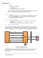
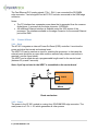
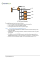
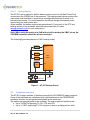
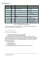
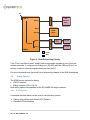
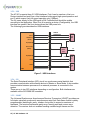
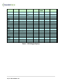
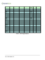
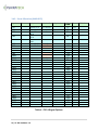
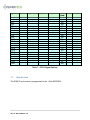
AT-901 ARM9 System on Module Hardware user manual Revision 1.0 Contents 1. Introduction ....................................................................................................................................... 4 2. AT-901 internal hardware description ........................................................................................ 4 Block Diagram ............................................................................................................................. 4 2.1. 2.2. 2.2.1. ARM-926EJ-S Processor........................................................................................................... 5 2.2.2. Memories ................................................................................................................................ 5 2.2.2.1. DDR2 ................................................................................................................................... 6 2.2.2.2. NAND flash .......................................................................................................................... 6 2.2.2.3. Micro SD .............................................................................................................................. 7 2.2.2.4. Other memory devices ....................................................................................................... 7 2.3. Build in Ethernet interface .......................................................................................................... 7 2.4. Power & Reset ............................................................................................................................. 8 2.4.1. Reset........................................................................................................................................ 8 2.4.2. Power ...................................................................................................................................... 8 2.4.2.1. Power signals on the SO-DIMM connector......................................................................... 9 2.4.2.2. Backup battery .................................................................................................................. 10 2.5. 3. AT-901 System ............................................................................................................................. 5 Extension connector .................................................................................................................. 10 Hardware Software interface....................................................................................................... 11 3.1. Hardware Configuration ............................................................................................................ 11 3.2. Interrupt & I/O Table ................................................................................................................. 11 3.3. Booting Sequence ...................................................................................................................... 12 3.4. Debug Options ........................................................................................................................... 13 3.4.1. JTAG Interface ....................................................................................................................... 13 3.4.2. Debug Interface ..................................................................................................................... 14 3.5. Interfaces ................................................................................................................................... 14 3.5.1. Ethernet................................................................................................................................. 14 3.5.2. I2C.......................................................................................................................................... 14 3.5.3. USB ........................................................................................................................................ 15 3.5.4. SPI .......................................................................................................................................... 15 2 | AT-901 Hardware 1.0 3.5.5. USART .................................................................................................................................... 15 3.5.6. UART ...................................................................................................................................... 16 3.5.7. HSMCI .................................................................................................................................... 16 3.6. GPIO Ports Allocation ................................................................................................................ 17 3.6.1. Ports Allocation (SAM9-G25) ................................................................................................ 17 3.6.2. Ports Allocation (SAM9-X35) ................................................................................................. 21 3.7. Identification ............................................................................................................................. 24 3 | AT-901 Hardware 1.0 1. Introduction The AT- 901 is an industrial embedded System-On-Module using the latest ARM and Linux technology. It is designed to serve as the controller and processing building block for embedded devices in applications such as medical devices, communications and industrial automation. The module can be provided with several levels of software integration starting from an ‘out of the box’ Debian Linux and up to a full software solution. Features: Using the SAM9Gx@400Mhz from Atmel offering a unique combination of an ARM9 processor combined with DDR2 for both enhanced performance and low cost solution. The card offers two processor types : o AT91SAM9G25 o AT91SAM9X35 – for touch screen and CAN interface support RAM - 128 MB DDR2 Flash - 256 MB NAND Flash A large variety of internal interfaces over a 200 pin SO-DIMM. 2. AT-901 internal hardware description 2.1. Block Diagram The following figure describes the AT-901 block diagram 3 x USB RMII NAND (Boot) FE 8 Bits CPU I/Os Options: DDR2 16 Bits RTC Opt. Supper CAP Power 3.3 V AT-901 Block Diagram 4 | AT-901 Hardware 1.0 2 0 0 1 x RMII 4 x UART (RX, TX, CTS, RTS) 2 x SPI (3 CS) 2 x SD/MMC card 2 x I2C 8 x A to D 40 I/Os Other S O D I M M The AT-901 block diagram includes: AT-901 system. AT-901 FE interface. AT-901 power & Reset. AT-901 extension connector. The following paragraphs describe each part of the system in details. 2.2. AT-901 System 2.2.1. ARM-926EJ-S Processor The AT-901 uses Atmel's SAM-9 ARM9 based series. The SAM-9 is a family of processors which uses an enhanced version of the ARM-926EJ-S processor. The SAM-9 support different flavors e.g. Single/dual Ethernet, enhanced graphic accelerator, LCD and more. All those flavors are footprint compatible and can be supported by the AT-901 module. The SAM-9 main features are: 400 MHZ core frequency (400 MIPS) 16 Kbytes data and instruction cache System running at 133 MHz Integrated RTC, POR and WDT Low power mode Multiplex peripherals bus 217 pins BGA package For full data sheet, use the following links: http://www.atmel.com/devices/SAM9G25.aspx?tab=documents http://www.atmel.com/devices/SAM9X35.aspx?tab=documents 2.2.2. Memories The AT-901 includes several types of memory for supporting booting, program execution and ID. The following figure describes the memories available on the AT-901. 5 | AT-901 Hardware 1.0 16 Bits DDR2 D[16:23] ½ - 2 GBits 133 MHz 8 Bits 2 GBits NAND (Boot) I2C 0 I2C PB-18 One Wire 1 Kbits O.W (MAC) SO-DIMM 200 MMC0 EEPROM (ID) 4 Bits uSD (Optional Boot) SAM-9 AT-901 Memory configuration 2.2.2.1. DDR2 The AT-901 a incorporate a 16 bits wide DDR2 for its program execution. The following are the DDR2 main features: Up to 2GBits. 16 bits data bus Support for 8 banks Up to 133 MHz clock Uses CS1 ODT not supported OCD not supported The default configuration includes 128M bytes, it can be enlarge to 256M bytes (ordering option). 2.2.2.2. NAND flash The AT-901 incorporates 8 bits wide NAND flash. The NAND is an SLC raw data NAND. It stores the AT-901 second level boot in a secured sector and 2 last versions of the application SW. It uses data signals D [16-23]. The main features of the NAND flash: 8 bits data bus. Up to 2Gbits memory volume 6 | AT-901 Hardware 1.0 CS3 Uses data bits D[16-23] 3.3V interfaces. The default configuration is 256M bytes Note – The SOM's NAND flash is from Toshiba. Any assembled flash need to be either from Toshiba or to support the ONFI (JEDEC) standard. 2.2.2.3. Micro SD The AT-901 has an option to run the software from a Micro SD. It uses MC0 of the PROCESSOR with up to 4 data lines. The Micro SD is connected through the SO-DIMM 200 connector. 2.2.2.4. Other memory devices o A one wire device which holds a build in unique ID , along with board information. o The AT-901 has an EEPROM option - Currently not available. 2.3. Build in Ethernet interface The AT-901 supports a build in Fast Ethernet interface, including a build in physical layer transceiver (PHY). The transceiver uses an RMII interface to interconnect with the processor’s Ethernet port 0. The following figure describes the Fast Ethernet interface. 2 x TX RMII 50 Mhz Ethernet 0 2 x RX Micrel ksz8051 RX Controls LEDS FE LEDS Int. PB-8 SAM-9 SO-DIMM 200 TX Controls NReset 25M Fast Ethernet RMII Interface The RMII interface is running at 50 MHz. The 50 MHz clock is generated by the Fast Ethernet PHY. PB-8 of the PROCESSOR uses as an interrupt input for the Fast Ethernet PHY. 7 | AT-901 Hardware 1.0 RJ45 MAG The Fast Ethernet PHY analog signals (TX+/-, RX+/-) are connected the SO-DIMM edge connector. Two led signal from the FE PHY are also connected to the SOM edge connector. Notes: The FE interface has a separate power plane that is separated from the common digital plane. It sources from the edge connector (VDDANA). An additional Ethernet interface is available using the X25 version of the processor. The interface available on the edge connector for the second Ethernet port will be RMII. 2.4. Power & Reset 2.4.1. Reset The AT-901 integrates an internal Power-On-Reset (POR) controller. It monitors the power and drive the internal and external reset. The NRST I/O can be used as an input for resetting the processor. In that case the external reset should be an open drain solution asserted only when a reset action is required ( see the figure below). The NRST can be used also as a programmable length reset for the carrier board (between 60 μs and 2 seconds). Note: A pull up resistor for the NRST is assembled on the carrier board. Push Button PU POR SAM-9 NReset Reset mechanism 2.4.2. Power The power to the AT-901 module is coming from SO-DIMM 200 edge connector. The main power is a 3.3V +/- 5% which generates all other powers. 8 | AT-901 Hardware 1.0 Power Enable 3.3 V 3.3 V (2-3A) EN I/O TPS62560 (TI) 3.3 -> 1.8 DDR TPS62560 (TI) 3.3 -> 1 Core TPS71710 (TI) 3.3 -> 1 (LDO) PLL AT-901 Power Hierarchy The available power levels used are as follows: The 1V is used to power the processor internal core and the 1.8V is used for to power the DDR2 interfaces. All I/O signals are fed from the 3.3V power supply. 2.4.2.1. Power signals on the SO-DIMM connector The power signals VDDIOP0 and VDDNF should be connected directly to the 3.3V power plane. VDDANA, power for Analog interfaces, should be connected to the 3.3V plane using a filter. The VBAT pin on the SO-DIMM connector should be either connected to an external battery located on the carrier board or shortens to 3.3V power source. ADREF is the A/D reference voltage, if not used connect directly to 3.3V 9 | AT-901 Hardware 1.0 2.4.2.2. Backup battery The AT-901 has an option for build in backup power source for the Real-Time-Clock connected to the VDDBU pin of the processor. The backup power device monitors the main power level and when it drops below a configurable threshold it switch to its internal power source. On normal operation the device charges the internal power source using the main power input. When installed, the battery supports an approximately 1 hour work of the RTC and backup section of the processor when the main power fails. (Contact [email protected] for more information). Note: When using the option of a SoM with a build in battery the VBAT pin on the SO-DIMM connector should be left un-connected. The following figure describes the AT-901 backup power: Filter VDDANA VDDIOP0, VDDNF I/O 3.3 -> 1.8 DDR 3.3 -> 1 Core CBC 3112 VBAT Atmel SAM-9 SO-DIMM 200 3.3V VBAT Shutdown WakeUp Inlet Figure 1 - AT-901 Backup Power 2.5. Extension connector The AT-901 support varieties of interfaces through the SO-DIMM 200 edge connector. Some of the interfaces are multiplexed with other interfaces on the PROCESSOR processor and thus not all options are available at the same time The options are preconfigured by the software. The main supported interfaces are: Up to 3 USART supporting TX, RX, CTS and RTS Up to 3 UART supporting TX, RX only(one of them is a debug port as well) 10 | AT-901 Hardware 1.0 Up to 2 Fast Ethernet port(an additional Ethernet port is available only with the X25 version – different ordering option) o Port 0 – TX+/-, RX+/o Port 1 - RMII Up to 2 SPI interfaces with 2 Chip Select each. Up to two I2C interfaces Up to 2 SDIO/MMC ports supporting 4 data bits each Up to 6 A to D convertors with 10 bits resolution and 100 KHz sampling rate Other optional interfaces are: o LCD monitor(X35 only) o Touch screen(X35 only) o Audio. o CAN interface (X35 only) o Others GPIOs – any un used pin can be configured as a GPIO for various control and monitor functions 3. Hardware Software interface 3.1. Hardware Configuration During power up some I/O bits status is latch to configure the CPU. The following table describes the bits and their functionality. Signal BMS (SOM) JTAG Select (Carrier) ETH0 Address EEPROM I2C Description 0 – Booting from CS0 using parallel NOR 1 – Booting from internal ROM 0 – Normal JTAG chain 1 – ICE mode The access address to the Ethernet 0 PHY The access address to the I2C EEPROM Default The AT-901 is always boot from the internal ROM. According to the pin connected to the connector 0001 1010001 Table 1 – HW Configured After Reset 3.2. Interrupt & I/O Table The following table describes the AT-901 dedicated I/O configuration. Some of the configurations are valid only when the relevant interfaces are assembled e.g. Ethernet and USB. When not assembled these pins can be used as I/Os. 11 | AT-901 Hardware 1.0 Signal E0 INTR E1 INTR MCI0 CD I/O PB-8 PC-26 PD-15 Description Ethernet 0 interrupt Ethernet 1 interrupt uSD card detect MCI1 CD PD-14 SD card detect VBUS Sense PB-16 USB port A power sense OverCur USB PB-17 EN5V HDA# PD-18 USB port A or Port B over current USB port A power drive enable EN5V HDB# PD-19 USB port B power drive enable EN5V HDC# PD-20 USB port C power drive enable Remarks Active Low Active Low 0 – Card in 1 – No card 0 – Card in 1 – No card 0 – No power sensed 1 – Power sensed Open Drain 0 – Enable 1 – Disable (Default) 0 – Enable 1 – Disable (Default) 0 – Enable 1 – Disable (Default) Table 2 – Configured I/O and Interrupts NOTE – More interrupts are available through the PROCESSOR I/O pins and can be configured according to the user application. 3.3. Booting Sequence The AT-901 has 3 boot phases: First level boot loader running from internal ROM. Device configuration running from internal RAM. SW downloads from NVRAM (NAND or SD Card) to DDR2 and execution. After POR the processor runs the "First Level Boot loader" program stored in its internal ROM. The program configures the SAM-9 clocks and looks for executable program in one of the non-volatile memories (See SAM-9 datasheet for a "valid" code for each of the optional memories). The optional memories are: NAND (Default). Micro SD card (Carrier). Serial NOR (Carrier). The following figure describes the optional boot memories and its priorities. 12 | AT-901 Hardware 1.0 VCC SO-DIMM 200 BMS = 1 MMC 0 uSD (Optional Boot) D[0:7] NAND (Boot) D[16:23] SO-DIMM 200 DBUG SAM BA Port A USB <-> RS-232 USB (A/B) USB (A/B) SAM-9 Carrier SOM Figure 2 - Boot Sequancing Priority If the "First Level Boot-Loader" doesn't find an executable program in one of the nonvolatile memories, it configures the Debug port (RS-232) and the USB port (Port 0 as device) to wait for external program download from the PC. For more information see the Atmel's boot sequencing chapter in the SAM-9 datasheet 3.4. Debug Options The SOM has two options for debug: JTAG Connector Debug interface (PA-9, PA-10) Both debug options are available on the SO-DIMM 200 edge connector. 3.4.1. JTAG Interface A standard interface which can be used for the following options: Debug using off-the-shelf Atmel's ICE (Default). Standard JTAG emulation. 13 | AT-901 Hardware 1.0 Choosing between the options is done by asserting the JTAGSEL signal available on the SO-DIMM edge connector. 3.4.2. Debug Interface The SAM-9 integrates an internal debug controller with UART interface (TX and RX signals only). 3.5. Interfaces 3.5.1. Ethernet The SAM9-G25/X35 support a single/dual Fast Ethernet interfaces. Each interface has its own MDC/MDIO controller. The default PHY address is 0001 for both interfaces. The MDC frequency is derived from the system clock and should not exceed 2.5MHz. 3.5.2. I2C There are up to three I2C interfaces dependent on PIO utilization The I2C main features are: One, Two or Three Bytes for Slave Address Sequential Read-write Operations Master, Multi-master and Slave Mode Operation Bit Rate: Up to 400 Kbits General Call Supported in Slave mode SMBUS Quick Command Supported in Master Mode Connection to DMA Controller (DMA) Channel Capabilities optimizes Data Transfers in Master Mode Only Standard Compliances 14 | AT-901 Hardware 1.0 3.5.3. USB The AT-901 supports three 2.0 USB interfaces. Port A can be used as a Host or a Device interface and port B as a Host interface both support high speed operation and port C which support only full speed operation only (12Mbps). The 5V power supply for the USB ports is SW Controlled and should be enable according to the application. When Port-A is used as a device (Configurable), the USB interface can sense if the Host device drives the USB power bus. The following figure describes the USB interfaces. USB 2.0 Host/Device USB A Type A/B VUSB Sense (PB-16) 5V/0.5A Over Current (PB-17) SO-DIMM 200 EN_A (PD-18) Current Limiter 0.5A 5V EN_B (PD-19) 5V/0.5A USB B USB C Type A Type A SAM-9 Figure 3 - USB interfaces 3.5.4. SPI The Serial Peripheral Interface (SPI) circuit is a synchronous serial data link that provides communication with external devices in Master or Slave Mode. It also enables communication between processors if an external processor is connected to the system. There are up to two SPI interfaces depending on configuration. Both interfaces are available on the SO-DIMM 200 connector. 3.5.5. USART The Universal Synchronous Asynchronous Receiver Transceiver (USART) provides one full duplex universal synchronous asynchronous serial link. Data frame format is widely programmable (data length, parity, number of stop bits) to support a maximum of standards. The receiver implements parity error, framing error and overrun error detection. The receiver time-out enables handling variable-length frames and the 15 | AT-901 Hardware 1.0 transmitter time guard facilitates communications with slow remote devices. Multidrop communications are also supported through address bit handling in reception and transmission. 3.5.6. UART The Universal Asynchronous Receiver Transmitter features a two-pin UART that can be used for communication and trace purposes. Moreover, the association with two DMA controller channels permits packet handling for these tasks with processor time reduced to a minimum. 3.5.7. HSMCI The High Speed Multi Media Card Interface (HSMCI) supports the Multi Media Card (MMC) Specification V4.3, the SD Memory Card Specification V2.0, the SDIO V2.0 specification and CE-ATA V1.1. 16 | AT-901 Hardware 1.0 3.6. GPIO Ports Allocation The processor has several flavors each with a different set of optional interfaces. The following tables describe the interfaces available in each option. In bold are the "FIXED" options that can't be changed. 3.6.1. Ports Allocation (SAM9-G25) Signal Alternate PA0 PA1 PA2 PA3 PA4 PA5 PA6 PA7 PA8 PA9 PA10 PA11 PA12 PA13 PA14 PA15 PA16 PA17 PA18 PA19 PA20 PA21 PA22 PA23 PA24 PA25 PA26 PA27 PA28 PA29 PA30 PA31 Option A Option B USART0 TX USART0 RX USART0 RTS USART0 CTS USART0 CLK USART1 TX USART1 RX USART2 TX USART2 RX DGB RX DBG TX SPI0 MISO SPI0 MOSI SPI0 SPCK SPI0 NPCS0 MCI0 D0 MCI0 CDA MCI0 CK MCI0 D1 MCI0 D2 MCI0 D3 TIOA0 TIOA1 TIOA2 TCLK0 TCLK1 TCLK2 TIOB0 TIOB1 TIOB2 I2C0 D I2C0 CK SPI1 NPCS1 SPI0 NPCS2 MCI1 D1 Option C ETX0 SODIMM 89 90 91 3.3V 3.3V 3.3V MCI1 D2 ETX1 92 3.3V MCI1 D3 ETXER 93 3.3V EMDC ETXEN 115 116 100 101 118 119 95 96 97 98 108 109 110 111 112 113 102 103 104 120 121 122 123 124 125 106 105 3.3V 3.3V 3.3V 3.3V 3.3V 3.3V 3.3V 3.3V 3.3V 3.3V 3.3V 3.3V 3.3V 3.3V 3.3V 3.3V 3.3V 3.3V 3.3V 3.3V 3.3V 3.3V 3.3V 3.3V 3.3V 3.3V 3.3V SPI0 NPCS1 SPI1 NPCS0 MCI1 D0 MCI1 CDA MCI1 CK SPI1 MISO SPI1 MOSI SPI1 SPK TK TF TD RD RK RF SPI1 NPCS3 SPI1 NPCS2 Table 3 – PIO A signal Options 17 | AT-901 Hardware 1.0 Power REMARK uSD Card uSD Card uSD Card uSD Card uSD Card uSD Card Signal Alternate Option A PB0 ETH0 RX0 PB1 ETH0 RX1 PB2 PB3 PB4 PB5 PB6 PB7 PB8 PB9 PB10 PB11 PB12 PB13 PB14 PB15 PB16 PB17 PB18 ETH0 RXER ETH0 RXDV ETH0 TXCK ETH0 MDIO ETH0 MDC ETH0 TXEN ETH0 TXER ETH0 TX0 ETH0 TX1 ETH0 TX2 ETH0 TX3 ETH0 RX2 ETH0 RX3 ETH0 RXCK ETH0 CRS ETH0 COL IRQ AD7 AD8 AD9 AD10 AD11 AD0 AD1 AD2 AD3 AD4 AD5 AD6 Option B Option C USART2 RTS USART2 CTS USART2 CK SPI0 NPCS3 I2C2 D I2C2 CLK PCK1 PCK0 PMW0 PMW1 PMW2 PMW3 ADTRG Table 1 - PIO B Signal Options 18 | AT-901 Hardware 1.0 SODIMM NA Power REMARK VDDANA ETH0 RMII NA VDDANA ETH0RMII NA NA NA 174 175 NA NA NA NA 181 182 183 184 185 186 187 189 VDDANA VDDANA VDDANA VDDANA VDDANA VDDANA VDDANA VDDANA VDDANA VDDANA VDDANA VDDANA VDDANA VDDANA VDDANA VDDANA VDDANA ETH0RMII ETH0RMII ETH0RMII ETH0RMII ETH0RMII ETH0RMII ETH0 Int. ETH0RMII ETH0RMII VBUS Sense Over Current Signal Alternate Option A PC0 PC1 PC2 PC3 PC4 PC5 PC6 PC7 PC8 PC9 PC10 PC11 PC12 PC13 PC14 PC15 PC16 PC17 PC18 PC19 PC20 PC21 PC22 PC23 PC24 Option C ISI D0 ISI D1 ISI D2 ISI D3 ISI D4 ISI D5 ISI D6 ISI D7 ISI D8 ISI D9 ISI D10 ISI D11 ISI PCK ISI VSYNC ISI HSYNC ISI MCK I2C1 D I2C1 CK TIOA3 TIOB3 TCLK3 TIOA4 TIOB4 TCLK4 UART0 TX UART0 RX PMW0 PMW1 TIOA5 TIOB5 TCLK5 PCK0 UART1 TX UART1 RX PMW0 PMW1 PMW2 PMW3 USART3 TX USART3 RX USART3 RTS USART3 CTS USART3 SCK PC25 PC26 USART1 RTS USART1 CTS USART1 SCK PC27 PC28 PC29 PC30 PC31 Option B FIQ PCK1 Table 2 - PIO C Signal Options 19 | AT-901 Hardware 1.0 SODIMM 129 130 131 132 133 134 136 137 138 139 140 141 143 144 145 146 148 149 150 151 152 153 155 156 157 Power 3.3V 3.3V 3.3V 3.3V 3.3V 3.3V 3.3V 3.3V 3.3V 3.3V 3.3V 3.3V 3.3V 3.3V 3.3V 3.3V 3.3V 3.3V 3.3V 3.3V 3.3V 3.3V 3.3V 3.3V 3.3V 158 3.3V 159 3.3V 160 3.3V 162 3.3V 163 3.3V 164 165 3.3V 3.3V REMARK Signal Alternate PD0 PD1 PD2 PD3 PD4 PD5 PD6 PD7 PD8 PD9 PD10 PD11 PD12 PD13 PD14 PD15 PD16 PD17 PD18 PD19 PD20 PD21 Option A NANDOE NANDWE NANDALE NANDCLE NCS3 NWAIT D16 D17 D18 D19 D20 D21 D22 D23 D24 D25 D26 D27 D28 D29 D30 D31 Option B Option C NA NA NA NA NA NA NA NA NA NA NA NA NA A20 A23 A24 A25 NCS2 NCS4 NCS5 Table 3 - PIO D Signal Options 20 | AT-901 Hardware 1.0 SODIMM NA 79 80 81 82 83 84 85 NA Power REMARK 3.3V 3.3V 3.3V 3.3V 3.3V 3.3V 3.3V 3.3V 3.3V 3.3V 3.3V 3.3V 3.3V 3.3V 3.3V 3.3V 3.3V 3.3V 3.3V 3.3V 3.3V 3.3V NAND NAND NAND NAND NAND NAND NAND NAND NAND NAND NAND NAND NAND NAND MCI1 CD MCI0 CD EN5V A EN5V B EN5V C 3.6.2. Ports Allocation (SAM9-X35) Signal Alternate PA0 PA1 PA2 PA3 PA4 PA5 PA6 PA7 PA8 PA9 PA10 PA11 PA12 PA13 PA14 PA15 PA16 PA17 PA18 PA19 PA20 PA21 PA22 PA23 PA24 PA25 PA26 PA27 PA28 PA29 PA30 PA31 Option A Option B USART0 TX USART0 RX USART0 RTS USART0 CTS USART0 CLK USART1 TX USART1 RX USART2 TX USART2 RX DGB RX DBG TX SPI0 MISO SPI0 MOSI SPI0 SPCK SPI0 NPCS0 MCI0 D0 MCI0 CDA MCI0 CK MCI0 D1 MCI0 D2 MCI0 D3 TIOA0 TIOA1 TIOA2 TCLK0 TCLK1 TCLK2 TIOB0 TIOB1 TIOB2 I2C0 D I2C0 CK SPI1 NPCS1 SPI0 NPCS2 MCI1 D1 Option C Power ETX0 89 90 91 3.3V 3.3V 3.3V MCI1 D2 ETX1 92 3.3V MCI1 D3 ETXER 93 3.3V EMDC ETXEN 115 116 100 101 118 119 95 96 97 98 108 109 110 111 112 113 102 103 104 120 121 122 123 124 125 106 105 3.3V 3.3V 3.3V 3.3V 3.3V 3.3V 3.3V 3.3V 3.3V 3.3V 3.3V 3.3V 3.3V 3.3V 3.3V 3.3V 3.3V 3.3V 3.3V 3.3V 3.3V 3.3V 3.3V 3.3V 3.3V 3.3V 3.3V CAN1 TX CAN1 RX SPI0 NPCS1 SPI1 NPCS0 CAN0RX CAN0 TX MCI1 D0 MCI1 CDA MCI1 CK SPI1 MISO SPI1 MOSI SPI1 SPK TK TF TD RD RK RF SPI1 NPCS3 SPI1 NPCS2 Table 4 - PIO A Signal Options 21 | AT-901 Hardware 1.0 SODIMM REMARK Signal Alternate Option A PB0 ETH0 RX0 PB1 ETH0 RX1 PB2 PB3 PB4 PB5 PB6 PB7 PB8 PB9 PB10 PB11 PB12 PB13 PB14 PB15 PB16 PB17 PB18 ETH0 RXER ETH0 RXDV ETH0 TXCK ETH0 MDIO ETH0 MDC ETH0 TXEN ETH0 TXER ETH0 TX0 ETH0 TX1 ETH0 TX2 ETH0 TX3 ETH0 RX2 ETH0 RX3 ETH0 RXCK ETH0 CRS ETH0 COL IRQ AD7 AD8 AD9 AD10 AD11 AD0 AD1 AD2 AD3 AD4 AD5 AD6 Option B Option C USART2 RTS USART2 CTS USART2 CK SPI0 NPCS3 I2C2 D I2C2 CLK PCK1 PCK0 PMW0 PMW1 PMW2 PMW3 ADTRG Table 5 - PIO B Signal Options 22 | AT-901 Hardware 1.0 SODIMM Power NA VDDANA NA VDDANA NA NA NA 174 175 NA NA NA NA 181 182 183 184 185 186 187 189 VDDANA VDDANA VDDANA VDDANA VDDANA VDDANA VDDANA VDDANA VDDANA VDDANA VDDANA VDDANA VDDANA VDDANA VDDANA VDDANA VDDANA REMARK Signal Alternate PC0 PC1 PC2 PC3 PC4 PC5 PC6 PC7 PC8 PC9 PC10 PC11 PC12 PC13 PC14 PC15 PC16 PC17 PC18 PC19 PC20 PC21 PC22 PC23 PC24 PC25 PC26 PC27 Option A LCDAT0 LCDAT1 LCDAT2 LCDAT3 LCDAT4 LCDAT5 LCDAT6 LCDAT7 LCDAT8 LCDAT9 LCDAT10 LCDAT11 LCDAT12 LCDAT13 LCDAT14 LCDAT15 LCDAT16 LCDAT17 LCDAT18 LCDAT19 LCDAT20 LCDAT21 LCDAT22 LCDAT23 LCDDISP PC29 LCDPWM LCDVSYN C LCDHSYN C LCDDEN PC30 PC31 LCDPCK FIQ PC28 Option B Option C I2C1 D I2C1 CK TIOA3 TIOB3 TCLK3 TIOA4 TIOB4 TCLK4 UART0 TX UART0 RX PMW0 PMW1 TIOA5 TIOB5 TCLK5 PCK0 UART1 TX UART1 RX PMW0 PMW1 PMW2 PMW3 Power 129 130 131 132 133 134 136 137 138 139 140 141 143 144 145 146 148 149 150 151 152 153 155 156 157 158 159 160 3.3V 3.3V 3.3V 3.3V 3.3V 3.3V 3.3V 3.3V 3.3V 3.3V 3.3V 3.3V 3.3V 3.3V 3.3V 3.3V 3.3V 3.3V 3.3V 3.3V 3.3V 3.3V 3.3V 3.3V 3.3V 3.3V 3.3V 3.3V USART1 CTS 162 3.3V USART1 SCK 163 3.3V 164 165 3.3V 3.3V USART1 RTS PCK1 Table 6 - PIO C Signal Options 23 | AT-901 Hardware 1.0 SODIMM REMARK Signal Alternate Option A NANDOE NANDWE NANDALE NANDCLE NCS3 NWAIT D16 D17 D18 D19 D20 D21 D22 D23 D24 D25 D26 D27 D28 D29 D30 D31 PD0 PD1 PD2 PD3 PD4 PD5 PD6 PD7 PD8 PD9 PD10 PD11 PD12 PD13 PD14 PD15 PD16 PD17 PD18 PD19 PD20 PD21 Option B Option C A20 A23 A24 A25 NCS2 NCS4 NCS5 SODIMM NA NA NA NA NA NA NA NA NA NA NA NA NA NA 79 80 81 82 83 84 85 NA Table 7 - PIO D Signal Options 3.7. Identification The SOM ID and version is programmed in the 1 Wire EEPROM. 24 | AT-901 Hardware 1.0 Power 3.3V 3.3V 3.3V 3.3V 3.3V 3.3V 3.3V 3.3V 3.3V 3.3V 3.3V 3.3V 3.3V 3.3V 3.3V 3.3V 3.3V 3.3V 3.3V 3.3V 3.3V 3.3V REMARK