1
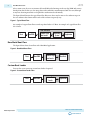
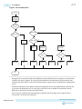
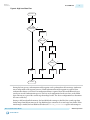
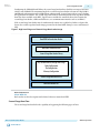
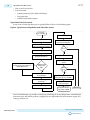
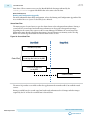
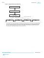
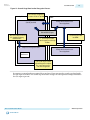
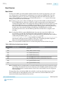
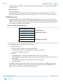
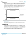
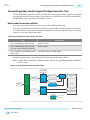
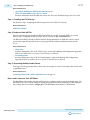
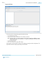
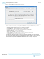
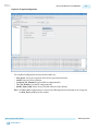
Arria 10 SoC Boot User Guide
2015.10.30
UG-1171
Subscribe
Send Feedback
This document provides comprehensive information on boot flow, boot source devices and how to
generate and debug a bootloader for the Arria® 10 SoC.
The details provided in this SoC boot user guide are:
• Typical boot flows supported by the Arria 10 SoC system
• Available boot source devices and their configuration information
• First and second boot stages (U-Boot or Unified Extensible Firmware Interface (UEFI))
•
•
•
•
Note: Although U-Boot is the primary example covered in this user guide, using UEFI as a secondstage non-general public license (non-GPL) boot loader source is also introduced. See
"Appendix B: Building the UEFI Boot Loader" for more information.
How to generate a boot loader and configure for a boot source device
How to build a boot loader
Debugging a boot loader
Technical reference appendices for boot memories and the SoC development platform
Related Information
Appendix B: Building the UEFI Boot Loader on page 39
Boot Process
Typical Boot Flow
The booting of the HPS is a multi-stage process. Each stage is responsible for loading the next stage.
The first stage is the boot ROM execution. The boot ROM code, located in the HPS, brings the processor
out of reset, puts the processor into a known and stable state, finds the second-stage boot loader and
passes control to the next stage. The boot ROM code is only aware of the second-stage boot loader and
not aware of any potential subsequent software stages. During this time, the boot ROM also seamlessly
handles any error conditions.
The next stage is when control passes to the second-stage boot loader. The second-stage boot loader is
located external to the HPS, either in external flash memory or within the FPGA. If the FPGA is used, the
second stage boot loader can execute directly from the FPGA without the need to copy it to on-chip RAM.
The second-stage boot loader locates and loads the next stage software and so on.
Before control is passed to the second stage boot loader, it can be decrypted and/or authenticated if secure
boot is enabled.
© 2015 Altera Corporation. All rights reserved. ALTERA, ARRIA, CYCLONE, ENPIRION, MAX, MEGACORE, NIOS, QUARTUS and STRATIX words and logos are
trademarks of Altera Corporation and registered in the U.S. Patent and Trademark Office and in other countries. All other words and logos identified as
trademarks or service marks are the property of their respective holders as described at www.altera.com/common/legal.html. Altera warrants performance
of its semiconductor products to current specifications in accordance with Altera's standard warranty, but reserves the right to make changes to any
products and services at any time without notice. Altera assumes no responsibility or liability arising out of the application or use of any information,
product, or service described herein except as expressly agreed to in writing by Altera. Altera customers are advised to obtain the latest version of device
specifications before relying on any published information and before placing orders for products or services.
www.altera.com
101 Innovation Drive, San Jose, CA 95134
ISO
9001:2008
Registered
2
UG-1171
2015.10.30
Bare Metal Boot Flow
After a warm reset, the user can instruct the boot ROM to find an image in the on-chip RAM and execute
directly from that. In this case, the image that resides in RAM is unauthenticated and clear text, although
it may have been imported into on-chip RAM as authenticated code initially.
The figure below illustrates the typical boot flow. However, there may be more or less software stages in
the user software than shown and the roles of the software stages may vary.
Figure 1: Typical Boot Flow
An example of a typical boot flow second-stage boot loader is U-Boot. An example of a typical boot flow
OS is Linux.
User Software
Reset
Boot ROM
Second-Stage
Boot Loader
Operating
System
Application
Bare Metal Boot Flow
The figure below shows a boot flow with a BareMetal application.
Figure 2: BareMetal Boot Flow
Reset
Boot ROM
Second-Stage
Boot Loader
BareMetal
Custom Boot Loader
You can also create your own custom boot loader if required.
Figure 3: Custom Boot loader Flow
Reset
Altera Corporation
Boot ROM
Custom Boot
Loader
Application
Arria 10 SoC Boot User Guide
Send Feedback
UG-1171
2015.10.30
Boot Stages
3
Boot Stages
Reset
Reset precedes the boot stages and is an important part of device initialization. There are two different
reset types: cold reset and warm reset.
The FPGA portion of the SoC can trigger a warm or cold reset on completion of configuration.
The boot process begins when CPU0 in the MPU exits from the reset state. When CPU0 exits from reset,
it starts executing code at the reset exception address where the boot ROM code is located. CPU1 remains
in reset during this time and is brought out of reset by user software.
With warm reset, some software registers are preserved and the boot process may skip some steps
depending on software settings. In addition, on a warm reset, the second-stage boot loader has the ability
to be executed from on-chip RAM.
Related Information
• Reset Manager
For more information about software reset refer to the "Reset Manager" chapter in the Arria 10 Hard
Processor System Technical Reference Manual.
• Arria 10 Core Fabric and General Purpose I/Os Handbook
For more information about FPGA configuration and reset
First Stage: Boot ROM
The boot ROM code is 128 KB in size and located in on-chip ROM at addresses 0xFFFC0000 to
0xFFFDFFFF. The function of the boot ROM code is to determine the boot source, initialize the HPS after
a reset, and jump to the second-stage boot loader. If the second-stage boot loader image has already been
loaded from the flash memory to on-chip RAM, the boot ROM jumps to on-chip RAM location. The boot
ROM performs the following actions to initialize the HPS:
•
•
•
•
Enables instruction cache, branch predictor, floating point unit, and NEON vector unit of CPU0
Sets up the level 4 (L4) watchdog 0 timer
Configures dedicated pins based on Boot Select (BSEL) settings
Initializes the flash controller to default settings
When booting from flash memory, the boot ROM code uses the top 32 KB of the on-chip RAM as data
workspace. This area is reserved for the boot ROM code after a reset until the boot ROM code passes
software control to second-stage boot loader. The maximum second-stage boot loader size is 208 KB with
authentication and 224 KB without. For a warm boot from RAM or a boot from FPGA, the boot ROM
code does not reserve the top 32 KB of the on-chip RAM, and the user may place user data in this area
without being overwritten by the boot ROM.
Note: The boot ROM only initializes the portions within the 32 KB of on-chip RAM it uses. If ECC is
required by the second-stage boot loader in on-chip RAM, then you should enable the security fuse
that clears all RAMs on a cold reset. Refer to SoC Security chapter in the Arria 10 Hard Processor
System Technical Reference Manual for more information on secure fuses.
The boot process begins when CPU0 exits from the reset state. The boot ROM code only executes on
CPU0. CPU1 is held in reset until it is released by user software. When CPU0 exits from reset, it starts
executing code at the reset exception address.
Arria 10 SoC Boot User Guide
Send Feedback
Altera Corporation
4
Boot ROM Flow
UG-1171
2015.10.30
During boot ROM execution, the clock control fuse information is automatically sent to the Clock
Manager, the memory control fuse information is automatically sent to the Reset Manager and all other
fuse functions (authentication, encryption, private and public key source, hash functions) are stored in a
memory-mapped location for boot code to read. In normal operation, the boot ROM is mapped at the
reset exception address so code starts executing in the boot ROM.
When CPU0 exits the boot ROM code and starts executing user software, boot ROM access is disabled.
The user software executing on CPU0 must map the user software exception vectors to 0x0 (which was
previously mapped to the boot ROM exception vectors) and release CPU1 from reset, if required. When
CPU1 is released from reset, CPU1 executes the user software exception instead of the boot ROM.
Related Information
SoC Security
For more information about security fuses, refer to the SoC Security chapter Arria 10 Hard Processor
System Technical Reference Manual.
Boot ROM Flow
On a cold reset, the HPS boot process starts when CPU0 is released from reset (for example, on a power
up) and executes code in the internal boot ROM at the reset exception address, 0x00000000. The boot
ROM code brings the HPS out of reset and into a known state. After boot ROM code is exited, control
passes to the next stage of the boot software, referred to as the second-stage boot loader. The second-stage
boot loader can be customized and is typically stored external to the HPS in a nonvolatile flash-based
memory or in on-chip RAM within the FPGA. The second-stage boot loader can then load an OS,
BareMetal application or potentially a third-stage boot loader.
This section describes the software flow from reset until the boot ROM code passes software control to the
second-stage boot loader.
The code starts, initializes the system and then depending on the type of boot requested, it may attempt to
load the code into the on-chip RAM. If the load is successful, the second-stage boot loader code executes.
If the boot ROM fails to find code or fails in three subsequent load attempts, it spins, waiting for a
watchdog reset.
Altera Corporation
Arria 10 SoC Boot User Guide
Send Feedback
UG-1171
2015.10.30
Boot ROM Flow
5
Figure 4: Main Boot ROM Flow
Reset
Initialize System
Boot Type
Flash Boot
FPGA Boot
RAM Boot
Reserved Boot
High-Level
Boot
FPGA Boot
RAM Boot
Reserved Boot
Code Valid?
Error
No
Yes
Jump to Code
Spin Until
Watchdog Reset
Boot
The boot ROM always executes on CPU0. CPU1 is always held in reset while the main boot ROM code is
executing and is only released when required by system software.
As part of determining the boot type, the boot ROM executes a low-level boot flow. The boot ROM code
reads the security fuse to determine if the source of the second-stage boot is forced to be the FPGA. If a
non-authenticated FPGA boot or a non-CRC on-chip RAM boot is requested or the boot is invalid, it is
processed within the low-level boot flow. All other boot types are processed within the high-level boot
flow.
Arria 10 SoC Boot User Guide
Send Feedback
Altera Corporation
6
UG-1171
2015.10.30
Boot ROM Flow
Figure 5: Low-Level Boot Flow
Low-Level Boot
Read Current
Security Status in
Security Manager
Required to boot
from FPGA?
No
Yes
Must Authenticate?
RAM Boot Allowed?
No
No
Yes
Yes
Enable FPGA
Access
RAM Boot Valid?
No
Yes
RAM Boot
Read BSEL Pins
FPGA Boot?
Read BSEL Pins
No
FPGA Boot?
Yes
Boot Not Valid
FPGA Boot
Boot Valid
FPGA Boot
No
Yes
Boot Not Valid
FPGA Boot
Boot Not Valid
Boot
During the low-level portion of the boot ROM flow, the boot ROM reads the security fuses to determine if
an FPGA-only boot is required. If so, then the boot ROM must also determine if the fuses indicate that
authentication of the POF is needed. If no authentication is required, then a standard FPGA configuration
occurs.
If an FPGA-only boot is not required, then the boot ROM checks if an on-chip RAM boot is allowed. If it
is, then the boot ROM checks to see if the code is valid. If the code is invalid, the boot ROM reads the
BSEL pins to determine if it indicated an FPGA boot.
If the secure fuses indicate that authentication is required for the boot image, then a high-level boot
(executed in C code) must be performed.
Altera Corporation
Arria 10 SoC Boot User Guide
Send Feedback
UG-1171
2015.10.30
Boot ROM Flow
7
Figure 6: High-Level Boot Flow
High-Level Boot
Global
Initialization
Boot from FPGA
& no Authenticate?
Yes
No
Initialize Hardware
RAM Boot Valid?
No
Yes
RAM Boot
Initialize DMA
Load from flash
Valid Image?
No
Yes
No Error
No Error
No Error
Error
Continue Boot
During the boot process, authentication and decryption can be performed on the boot image. Authentica‐
tion is independent of decryption; however, if both authentication and decryption are required, then
authentication always occurs first. If an authenticated boot is required, then the boot ROM must have a
root key to start the authentication process. This key can be implemented in the user fuses, in the FPGA
logic elements or as part of the second-stage boot image header. The device configuration fuses determine
the source of the key.
During a cold boot from flash memory, the boot ROM code attempts to load the first second-stage boot
loader image from flash memory to on-chip RAM and pass control to the second-stage boot loader. If this
initial image is invalid, the boot ROM code indexes the romcode_initswlastld register and attempts to
Arria 10 SoC Boot User Guide
Send Feedback
Altera Corporation
8
UG-1171
2015.10.30
Second Stage: Boot Loader (U-Boot)
load the next stored image. The boot ROM will attempt three subsequent loads after the initial one. If
there is still no valid image found after the subsequent loads, the boot ROM code checks the FPGA
portion of the device for a fallback image.
Note: During the boot process, the boot ROM enables all of the caches (L1 data and instruction caches
and L2 cache). If the second-stage boot loader is not loaded from a boot flash device (SD/MMC,
QSPI, NAND) properly, the caches may be left on when the boot ROM checks the FPGA portion
the device for a fallback image. This situation can lead to issues of coherency when loading code, so
caches must be flushed and disabled in the fallback image.
If the warm RAM boot has failed or if a cold reset has occurred, then the boot ROM reads the BSEL value
in the bootinfo register of the System Manager. If the FPGA is selected as the boot source, then the boot
ROM code attempts to execute code at address 0xC0000000 across the HPS-to-FPGA bridge (offset
0x00000000 from bridge). No error conditions are generated if the FPGA does not initialize properly and
the watchdog is not enabled for time-out. Instead, the boot ROM continues to wait until the FPGA is
available.
If the BSEL bits indicate a boot from external flash, then the boot ROM code attempts to load an image
from a flash device into the on-chip RAM, verify and execute it. If the BSEL is invalid or the boot ROM
code cannot find a valid image in the flash, then the boot ROM code checks if there is a fallback image in
the FPGA. If there is, then the boot ROM executes the fallback image. If there is no fallback image then
the boot ROM performs a post-mortem dump of information into the on-chip RAM and awaits a reset.
Note: The acronyms BSEL and BOOTSEL are used interchangeably to define the boot select pins.
The boot ROM code verifies the second-stage boot loader in several ways to ensure a corrupted image is
not executed. The first test is of the image header, which identifies the magic number, version, block
length, and CRC of the image that protects the block. If any of these are invalid, an error occurs.
Second Stage: Boot Loader (U-Boot)
Note: This section pertains to feature information for U-Boot. For information on UEFI boot loader
features, refer to technical reference documentation for UEFI on Altera®'s wiki page.
The function of the second-stage boot loader is user-defined. The Altera-provided second-stage boot
loader is a combination of initialization, configuration and U-Boot code and contains features such as:
•
•
•
•
•
•
•
•
•
•
•
•
•
SD/MMC controller driver
QSPI controller driver
Ethernet driver plus protocol support
Drivers for system-level IP, such as Clock Manager, System Manager, and FPGA Manager
Cache memory drivers
UART, timer and watchdog drivers
FAT file system support
Flat Image Tree (FIT) image processing
U-Boot console support including basic essential debug commands
Cryptographic library
U-Boot device tree processing library
System and memory firewall configuration
Initialization code for the interface that loads the next stage of software
If a secure boot is required, the second-stage boot loader can be used to increase the level of security and
to authenticate and initiate decryption of the next boot image if necessary.
Altera Corporation
Arria 10 SoC Boot User Guide
Send Feedback
UG-1171
2015.10.30
Second-Stage Boot Flow
9
Configuring the SDRAM firewall allows the second-stage boot loader to load the next stage of the boot
software into SDRAM. The maximum length for a second-stage boot loader to fit into on-chip RAM is
208 KB with authentication and 224 KB without authentication. A typical next software stage is loading
the application OS software. The second-stage boot loader is allowed to load the next stage boot software
from any device available to the HPS. Typical sources include the same flash device that contains the
second stage boot loader, a different flash device, or a communication interface such as an EMAC.
If the second-stage boot loader must be authenticated, it must store a public key. Below is a figure that
depicts the second-stage boot loader image presented to the boot ROM, during a secure, authenticated
boot.
Figure 7: High-Level Diagram of Second-Stage Boot Loader Image
Boot ROM Authentication Header
Boot ROM Standard Header
Second-Stage Boot Loader Binary
Keys to Authenticate/Decrypt Next Stage
Clock Configuration
Pin Configuration
Memory Configuration
Second-Stage Boot Loader DTB
Boot ROM Header CRC
Related Information
Altera Wiki Site
Refer to this site for a description and technical reference material on UEFI.
Second-Stage Boot Flow
The second stage boot loader has the capability of supporting the following types of boot:
Arria 10 SoC Boot User Guide
Send Feedback
Altera Corporation
10
UG-1171
2015.10.30
Typical Boot Flow (Non-Secure)
• Non-secure clear text boot
• Secure boot with:
• Authentication only (also called verified boot)
• Decryption only
• Authentication and decryption
Typical Boot Flow (Non-Secure)
A non-secure second-stage boot process typically follows a flow as in the following figure.
Figure 8: Typical Second-Stage Boot Loader Flow (Non-Secure)
Second-Stage
Boot Loader Entry
Timer & UART Initialization
Low-Level Initialization
Assert Reset to Affected Peripherals/
Components during PLL Reconfiguration
Clock Reconfiguration
Configure Dedicated HPS I/O
Configure Shared HPS I/O & Hard Memory
Controller I/O Using Full or Early Release
FPGA Configuration Flow
SDRAM Interface Initialization (Include
Calibration & PLL Configuration)
Success? no
yes
Next Stage Boot Device Initialization
Checking Boot Image’s Checksum
(Optional)
no
FPGA Fabric and I/O
Configured Thru
FPGA?
yes
Configure Pin Multiplexing through
the System Manager
Reset Deassertion through the
Reset Manager
Checksum no
Passed?
yes
Copy the Next Stage Boot Image from the
Next Stage Boot Device to the SDRAM
Write Magic Value to the Initial
Software State Register
System Interconnect Configuration
Pass Control to Next Boot
Stage Software in SDRAM
Error Handler
Low-level initialization steps include reconfiguring or disabling the L4 watchdog 0 timer, invalidating the
instruction cache and branch predictor, remapping the on-chip RAM to the lowest memory region, and
setting up the data area.
Altera Corporation
Arria 10 SoC Boot User Guide
Send Feedback
UG-1171
2015.10.30
Typical Boot Flow (Non-Secure)
11
Upon entering the second-stage boot loader, the L4 watchdog 0 timer is active. The second stage boot
loader can disable, reconfigure, or leave the watchdog timer unchanged. Once enabled after reset, the
watchdog timer cannot be disabled, only paused or reset.
The instruction cache and branch predictor, which were previously enabled by the boot ROM code, must
be invalidated. If the second-stage boot loader enables and uses the data cache, it must initialize all levels
of the data cache before enabling.
The second-stage boot loader must remap the exception vector table because the exception vectors are still
pointing to the exception handler in the boot ROM when it starts executing. By setting the system
interconnect remap bit 0 to one, the on-chip RAM mirrors to the lowest region of the memory map. After
this remap, the exception vectors use the exception handlers in the boot loader image.
The figure below shows the memory map before and after remap.
Figure 9: Remapping the On-Chip RAM
Boot ROM
0xFFFF_FFFF
0xFFE0_0000
...
0xFFFD_FFFF
On-Chip ROM
0xFFFC_0000
...
0xBFFF_FFFF
SDRAM
0x0010_0000
Unused
0x0002_0000
On-Chip ROM
0x0000_0000
Before
On-Chip RAM
Second-Stage
Boot Loader
0xFFFF_FFFF
0xFFE0_0000
...
0xFFFD_FFFF
On-Chip ROM
0xFFFC_0000
...
0xBFFF_FFFF
SDRAM
0x0010_0000
Unused
0x0004_0000
On-Chip RAM
0x0000_0000
After
On-Chip RAM
The second-stage boot loader can reconfigure all HPS clocks. During clock reconfiguration, the boot
loader asserts reset to the peripherals in the HPS affected by the clock changes.
The I/O assignments for the HPS are configured as part of the IOCSR configuration in the second-stage
boot loader. Effectively, a bitstream containing the I/O assignments is sent to the device as part of the
initialization code in the second-stage boot loader. If the FPGA fabric and I/O have not yet been
configured through the FPGA and the HPS needs to access SDRAM, you should program the HPS to use
the full or early I/O release configuration method to configure the shared and hard memory controller
I/O. Refer to "FPGA Configuration" section of the "Booting and Configuration" appendix in the Arria 10
Hard Processor System Technical Reference Manual for details on full and early I/O release configuration.
The second-stage boot loader looks for a valid next-stage boot image in the next-stage boot device by
checking the boot image validation data and checksum in the mirror image. Once validated, the secondstage boot loader copies the next-stage boot image (OS or application image) from the next-stage boot
device to the SDRAM.
Before software passes control to the next-stage boot software, the second-stage boot loader can write a
valid value (0x49535756) to the romcode_initswstate register in the System Manager. This value
indicates that there is a valid boot image in the on-chip RAM. The romcode_initiswlastld register
holds the index of the last second-stage boot loader software image loaded by the Boot ROM from the
Arria 10 SoC Boot User Guide
Send Feedback
Altera Corporation
12
UG-1171
2015.10.30
Secure Boot Flow
boot device. When a warm reset occurs, the Boot ROM loads the image indicated by the
romcode_initswlastld register if the BSEL value is the same as the last boot.
Related Information
Booting and Configuration Appendix
For more information about flash configuration, refer to the Booting and Configuration Appendix of the
Arria 10 Hard Processor System Technical Reference Manual.
Secure Boot Flow
The main purpose of secure boot is to pass the chain of trust to the subsequent boot software. During a
secure boot, the second-stage boot loader may authenticate or decrypt the subsequent boot image,
depending on the current state registers in the Security Manager. In addition, the second-stage boot
loader must ensure that the subsequent boot image is executed from secure memory such as on-chip
RAM. The second-stage boot loader fits into the chain of trust as such:
Figure 10: Secure Boot Flow
Secure World
Normal World
Boot ROM (on-chip ROM)
Authenticate and/or Decrypt
Chain of Trust
Second-Stage Boot Loader (on-chip RAM)
Authenticate and/or Decrypt
Secure Micro-OS/ Application
(on-chip RAM)
Through Secure API
Standard OS (SDRAM)
The micro OS provides secure APIs to allow the application in the normal world OS to establish trusted
services.
During a verified boot, the second-stage boot loader only authenticates the OS image and other images
required by the OS. A flow for a verified boot is shown below.
Altera Corporation
Arria 10 SoC Boot User Guide
Send Feedback
UG-1171
2015.10.30
Secure Boot Flow
13
Figure 11: Verified (Authenticated) Boot Flow
Boot ROM (on-chip ROM)
Second-Stage Boot Loader (on-chip RAM)
Authenticate Only
OS Image (SDRAM)
Dotted lines represent files within OS Image
zImage
Device Tree Blob
Filesystem
Other
For both the secure and verified boot, the subsequent boot image must be executed in on-chip RAM while
the second-stage boot loader is still executing from on-chip RAM. In order to accommodate this require‐
ment, the authentication and decryption process might follow the following steps depicted in the next
three diagrams, depending on the type of secure boot chosen.
Arria 10 SoC Boot User Guide
Send Feedback
Altera Corporation
14
UG-1171
2015.10.30
Secure Boot Flow
Figure 12: Second-Stage Boot Loader Authentication Process
5. The secure micro OS/application
can consume all of the on-chip RAM
On-chip RAM
Second-Stage Boot Loader
(loaded by boot ROM)
3. Boot Loader collapses to the end
of on-chip RAM only keeping
the copy and SHA functions
2. Authenticate the image
and store the hash value
SDRAM
FIT Image which contains the secure
micro OS/application
4. The second-stage boot loader copies the
secure micro OS/application into on-chip RAM
and verifies it by matching the SHA. If it matches,
control is passed to micro OS/application
1. Load FIT image from flash
into SDRAM
Collapsed Second-Stage Boot Loader
FIT Image which contains the secure
micro OS/application
Copy Function
Altera Corporation
SHA Function
Arria 10 SoC Boot User Guide
Send Feedback
UG-1171
2015.10.30
Secure Boot Flow
15
Figure 13: Second-Stage Boot Loader Decryption Process
5. The secure micro OS/application
can consume all of the on-chip RAM
On-chip RAM
SDRAM
Second-Stage Boot Loader
(loaded by boot ROM)
FIT Image which contains the secure
micro OS/application
DMA and FPGA CSS Engine
2. Boot Loader collapses to the end
of on-chip RAM only keeping
the DMA function
3. Second-stage boot loader
starts decryption process through
CSS DMA
1. Load FIT image from flash
into SDRAM
Collapsed Second-Stage Boot Loader
FIT Image which contains the secure
micro OS/application
DMA Function
4. The second-stage boot loader
polls until decryption is completed.
Then, control can be passed to
secure micro OS/application
Decryption is optional and is not required for secure boot. Upon entry into the second-stage boot loader,
the CSS engine is enabled. The second-stage boot loader decrypts the subsequent boot image and disables
the CSS engine upon exit.
Arria 10 SoC Boot User Guide
Send Feedback
Altera Corporation
16
UG-1171
2015.10.30
Secure Boot Flow
Figure 14: Second-Stage Boot Loader Authentication and Decryption Process
4. Second-stage boot loader copies
secure micro OS/application into
on-chip RAM and verifies by
matching the SHA
On-chip RAM
SDRAM
Second-Stage Boot Loader
(loaded by boot ROM)
2. Authenticate the image
and store the hash value
FIT Image which contains the secure
micro OS/application
7. The secure micro OS/application
can consume all of the
on-chip memory.
DMA and FPGA CSS Engine
3. Boot Loader collapses to the end
of on-chip RAM only keeping
the copy, SHA, and DMA function
5. Second-stage boot loader
starts decryption process through
CSS DMA
1. Load FIT image from flash
into SDRAM
Collapsed Second-Stage Boot Loader
DMA Function
Copy Function
FIT Image which contains the secure
micro OS/application
SHA Function
6. The second-stage boot loader
polls until decryption is completed.
Then, control can be passed to
secure micro OS/application
Altera Corporation
Arria 10 SoC Boot User Guide
Send Feedback
UG-1171
2015.10.30
Boot Devices
17
Boot Devices
Boot Select
The boot select (BSEL) pins offer multiple methods to obtain the second-stage boot image. On a cold
reset, the boot source is determined by a combination of secure boot fuses and BSEL pins. These fuse
values and BSEL pin values are sent to the Security Manager module of the HPS when the cold reset
occurs. When the HPS is released from reset, the boot ROM reads the bootinfo register of the System
Manager to determine the source of the boot.
Note: If the fpga_boot_f fuse is blown, the BSEL pins are bypassed and the HPS can only boot from the
FPGA. Additionally, the clock select (CSEL) fuse values are ignored and clock configuration is
controlled through the FPGA. This configuration allows the HPS to boot from encrypted user code
in the FPGA. If the boot source is the FPGA, the boot ROM code does not configure any of the
boot-specific HPS I/Os for booting from flash memory. If the fpga_boot_f fuse is not blown, then
the boot source is determined according to the BSEL pins. If the BSEL pins are used for
determining the boot source, then the following table shows the flash devices assigned to each
encoding.
Note: If a boot from FPGA is required (BSEL[2:0]=0x1), then you must ensure that the HPS is not
released from reset until after the FPGA has been fully programmed. Otherwise, the bootinfo
register to determine the boot source might be read incorrectly by the boot ROM. FPGA readiness
is indicated by handshake signals, f2h_boot_from_fpga_ready and
f2h_boot_from_fpga_on_failure, from the FPGA to the HPS. The f2h_boot_from_fpga_ready
signal must be pulled up to indicate readiness. Refer to the "Instantiating the HPS Component"
chapter for more information about FPGA boot handshake signals.
Note: The acronyms BSEL and BOOTSEL are used interchangeably to define the boot select pins.
Table 1: BSEL Values for Boot Source Selection
BSEL[2:0] Value
Flash Device
0x0
Reserved
0x1
FPGA (HPS-to-FPGA bridge)
0x2
1.8 V NAND flash memory
0x3
3.0 V NAND flash memory
0x4
1.8 V SD/MMC flash memory with external transceiver
0x5
3.0 V SD/MMC flash memory with internal transceiver
0x6
1.8 V quad SPI flash memory
0x7
3.0 V quad SPI flash memory
Note: If the BSEL value is set to 0x4 or 0x5, an external translation transceiver may be required to supply
level-shifting and isolation if the SD cards interfacing to the SD/MMC controller must operate at a
different voltage than the controller interface. Please refer to the SD/MMC Controller chapter for
more information.
The typical boot flow is for the boot ROM code to find the second-stage boot loader image on a flash
device, load that into on-chip RAM and execute it. After a warm reset, the boot ROM code can be
instructed to find the image in RAM and execute that.
Arria 10 SoC Boot User Guide
Send Feedback
Altera Corporation
18
UG-1171
2015.10.30
Flash Memory Devices for Booting
The HPS flash sources can store various file types, such as:
•
•
•
•
FPGA programming files
Second-stage boot loader binary file (up to four copies)
Operating system binary files
Application file system
The second-stage boot loader image in flash can be authenticated and decrypted by the HPS. A boot
directly from the HPS on-chip RAM is always unauthenticated and in clear text, although it may have an
optional CRC if required.
When the BSEL value is 0x1, the FPGA is selected as the boot source for that boot. This selection is not
permanent as it is when the fpga_boot_f fuse is enabled. In both cases, the CSEL fuses are also ignored
and the HPS must be held in reset until the FPGA is powered on and programmed to prevent the boot
ROM from misinterpreting the boot source.
If an HPS flash interface has been selected to load the boot image, then the boot ROM enables and
configures that interface before loading the boot image into on-chip RAM, verifying it and passing
software control to the second-stage boot loader.
If the FPGA fabric is the boot source, the boot ROM code waits until the FPGA portion of the device is in
user mode, and is ready to execute code and then passes software control to the second-stage boot loader
in the FPGA RAM.
Flash Memory Devices for Booting
The memory controllers and devices that contain the boot loader image have configuration requirements
for proper boot from flash.
On all flash devices, there is an area of memory, called the boot area that contains up to four second-stage
boot loader images. For the QSPI and SD/MMC devices, the boot area is 1 MB in size. For NAND devices
the boot area is four device blocks in size and may be larger than 1 MB if the NAND erase block is larger
than 256 KB.
The SD/MMC, Quad SPI and NAND flash devices all support raw and MBR (partition) mode. In raw
mode, the boot image is located at the start of the flash memory device, at offset 0x0. In MBR mode:
• The boot image is read from a custom partition (0xA2)
• The first image is located at the beginning of the partition, at offset 0x0
• Start address = partition start address
Quad SPI Flash Devices
The figure below shows the quad SPI flash image layout. The second-stage boot loader image is always
located at offsets that are multiples of 256 KB.
Figure 15: Quad SPI Flash Image Layout
Second-Stage Boot Loader Image 3
Second-Stage Boot Loader Image 2
0x0
Altera Corporation
Second-Stage Boot Loader Image 1
Second-Stage Boot Loader Image 0
Multiple of 256 KB
Arria 10 SoC Boot User Guide
Send Feedback
UG-1171
2015.10.30
SD/MMC Flash Devices
19
The boot ROM code configures the quad SPI controller to default settings for the supported SPI or quad
SPI flash memory.
Related Information
Flash Memory Devices
For more information on default settings and CSEL pin settings for flash memory devices, refer to the
Booting and Configuration Appendix of the Arria 10 Hard Processor System Technical Reference Manual.
SD/MMC Flash Devices
The following figure shows an SD/MMC flash image layout example for boot. The master boot record
(MBR) is located in the first 512 bytes of the memory. The MBR contains information about the partitions
(address and size of partition). The second-stage boot loader image is stored in partition A2. Partition A2
is a custom raw partition with no file system.
Figure 16: SD/MMC Flash Image Layout
Second-Stage Boot Loader Image 3
Second-Stage Boot Loader Image 2
Second-Stage Boot Loader Image 1
0x0
Partition Type: A2
Partition Size: 256 KB x 4
Second-Stage Boot Loader Image 0
...
MBR Partition Size: 512 Bytes
Master Boot Record (MBR)
The SD/MMC controller supports two booting modes:
• MBR (partition) mode
• The boot image is read from a custom partition (0xA2)
• The first image is located at the beginning of the partition, at offset 0x0
• Start address = partition start address
• Raw mode
• If the MBR signature is not found, SD/MMC driver assumes it is in raw mode
• The boot image data is read directly from sectors in the user area and is located at the first sector of
the SD/MMC
• The first image is located at the start of the memory card, at offset 0x0
• Start address = 0x0
The MBR contains the partition table, which is always located in the first sector (LBA0) with a memory
size of 512 bytes. The MBR consists of executable code, four partition entries, and the MBR signature. A
MBR can be created by specific tools like the FDISK program.
Arria 10 SoC Boot User Guide
Send Feedback
Altera Corporation
20
UG-1171
2015.10.30
SD/MMC Flash Devices
Table 2: MBR Structure
Offset
Size (In Bytes)
Description
0x000
446
Code area
0x1BE
16
Partition entry for partition 1
0x1CE
16
Partition entry for partition 2
0x1DE
16
Partition entry for partition 3
0x1EE
16
Partition entry for partition 4
0x1FE
2
MBR signature: 0xAA55
The standard MBR structure contains a partition with four 16-byte entries. Thus, memory cards using this
standard table cannot have more than four primary partitions or up to three primary partitions and one
extended partition.
Each partition type is defined by the partition entry. The boot images are stored in a primary partition
with custom partition type (0xA2). The SD/MMC flash driver does not support a file system, so the boot
images are located in partition A2 at fixed locations.
Table 3: Partition Entry
Offset
Size (In Bytes)
Description
0x0
1
Boot indicator. 0x80 indicates
that it is bootable.
0x1
3
Starting CHS value
0x4
1
Partition type
0x5
3
Ending CHS value
0x8
4
LBA of first section in partition
0xB
4
Number of sectors in partition
The boot ROM code configures the SD/MMC controller to default settings for the supported SD/MMC
flash memory.
Related Information
Flash Memory Devices
For more information on default settings and CSEL pin settings for flash memory devices, refer to the
Booting and Configuration Appendix of the Arria 10 Hard Processor System Technical Reference Manual.
Altera Corporation
Arria 10 SoC Boot User Guide
Send Feedback
UG-1171
2015.10.30
NAND Flash Devices
21
NAND Flash Devices
The NAND subsystem reserves at least the first 1 MB on the NAND device. If the NAND flash device has
blocks greater than 256 KB, then the NAND subsystem reserves the first four blocks on the device. For a
NAND device with less than 256 KB block size, the second-stage boot loader image must be placed in
multiple blocks. The NAND subsystem expects to find up to four second-stage boot loader images on the
NAND device. You may have less than four images if required. The second-stage boot loader image
should always be at the start of a physical page. Because a block is the smallest area used for erase
operation, any update to a particular image does not affect other images.
Figure 17: NAND Flash Image Layout for 256 KB Memory Blocks
0xFFFFF
Second-Stage Boot Loader Image 3
0xC0000
Second-Stage Boot Loader Image 2
0x80000
Second-Stage Boot Loader Image 1
Each block available for
the boot loader image
is 256 KB
0x40000
Second-Stage Boot Loader Image 0
0x00000
Related Information
Flash Memory Devices
For more information on default settings and CSEL pin settings for flash memory devices, refer to the
Booting and Configuration Appendix of the Arria 10 Hard Processor System Technical Reference Manual.
Booting From FPGA
In the figure below, the FPGA is configured first through one of its non-HPS configuration sources. The
CSS block configures the FPGA fabric as well as the FPGA I/O, shared I/O and hard memory controller
I/O. The HPS executes the second-stage boot loader from the FPGA. In this situation, the HPS should not
be released from reset until the FPGA is powered on and programmed. Once the FPGA is in user mode
and the HPS has been released from reset, the boot ROM code begins executing. The HPS boot ROM code
executes the second-stage boot loader from the FPGA fabric over the HPS-to-FPGA bridge.
Arria 10 SoC Boot User Guide
Send Feedback
Altera Corporation
22
UG-1171
2015.10.30
Booting From FPGA
Figure 18: Boot From FPGA Flow
Shared I/O
CSS
Active Serial/
Active Serial x4
Boot &
Configuration
Sources
Passive
Serial
Passive
Parallel
MPU
FPGA
Fabric
Boot
ROM
JTAG
FPGA I/O
HPS-to-FPGA
Bridge
FPGA
HPS
HPS Dedicated I/O
PCIe
Hard Memory Controller I/O
Altera Corporation
Arria 10 SoC Boot User Guide
Send Feedback
UG-1171
2015.10.30
Second-Stage Boot Loader Support Package Generator Tool
23
Second-Stage Boot Loader Support Package Generator Tool
The SoC Embedded Design Suite (SoC EDS) includes the second-stage boot loader support package (BSP)
generator tool that allows you to generate a boot loader for your FPGA design. The boot generation flow
and BSP Editor tool are described in the following sections.
Boot Loader Generation and Flow
Generating a boot loader involves several steps to produce a final bootable image.
Each step is dependent on the previous one. Either the associated Altera Complete Design Suite (ACDS)
or SoC EDS tool is used to generate information required for the following dependent steps. See the table
below for a list of steps and associated tools:
Table 4: Boot Loader Generation Stages and Tools
Steps
Required Tool
Step 1: Compiling the FPGA Design
Quartus® Prime
Step 2: Identifying the hardware hard
processor system (HPS) hand-off files
Quartus Prime
Step 3: Generating and building a boot
loader source
SoC EDS tool chain and BSP Editor
The following figure depicts the complete boot loader generation flow using U-Boot.
Note: A similar flow is available for a UEFI boot loader. Refer to the "Appendix B: Building a UEFI Boot
Loader" section.
Figure 19: Arria 10 Boot Loader Generation Flow
User Options
U-Boot Device Tree
Handoff Folder
(XML Files)
make
U-Boot Binary
& U-Boot Device Tree
Image
BSP Editor
U-Boot Makefile
Hardware
Design
Quartus II
SD Card
U-Boot Source
Core RBF
SOF
Quartus
CPF
Peripheral RBF
Legend
Part of SoC EDS
Part of ACDS
Arria 10 SoC Boot User Guide
Send Feedback
Altera Corporation
24
UG-1171
2015.10.30
Step 1: Compiling the FPGA Design
Related Information
• Appendix B: Building the UEFI Boot Loader on page 39
• Altera SoC Embedded Design Suite User Guide
For more information about the BSP tools refer to the Altera SoC Embedded Design Suite User Guide.
Step 1: Compiling the FPGA Design
For details on Step 1: Compiling the FPGA Design refer to the GSRD User Manual.
Related Information
GSRD User Manual
Step 2: Hardware Hand-off Files
Prior to generating the boot loader, the HPS hand-off files are needed. The hand-off files are created
during "Step 1: Compiling the FPGA Design" and are saved in the hps_isw_handoff folder.
The HPS hand-off files contain the FPGA hardware design information (as XML files) and are used to
generate the required boot loader device tree for proper FPGA hardware initialization and run-time
access.
Related Information
• Clock Select
For more information, refer to the "Clock Selects" section in the Booting and Configuration Appendix
of the Arria 10 Hard Processor System Technical Reference Manual.
• I/O Configuration
For more information, refer to the "I/O Configuration" section in the Booting and Configuration
Appendix of the Arria 10 Hard Processor System Technical Reference Manual.
Step 3: Generating the Boot Loader Source
This step in the boot generation flow is discussed as an example in section "Generating a Boot Loader with
a QSPI Boot Device."
Related Information
Generating a Boot Loader with a QSPI Boot Device on page 28
Boot Loader Generator Tool: BSP Editor
The BSP Editor tool provides you with guided options to configure and generate a boot loader image. The
BSP Editor tool is also used for editing an existing generated boot loader by modifying the BSP configura‐
tion settings that are saved in the settings.bsp file. The BSP Editor main interface is shown below.
Altera Corporation
Arria 10 SoC Boot User Guide
Send Feedback
UG-1171
2015.10.30
Boot Loader Generator Tool: BSP Editor
25
Figure 20: BSP Editor
The tool provides the configuration options that include selecting:
• Associated HPS hand-off files
• Target OS (both U-Boot or UEFI boot use the U-Boot OS selection)
Note: Although U-Boot is the primary example covered in this user guide, using UEFI as a secondstage boot loader source is also introduced. See "Appendix B: Building the UEFI Boot Loader"
for more information.
• Locations for boot loader
• Source and configuration settings (BSP settings).
These options are present whether creating a new or editing an existing boot loader configuration. The
figure below shows the settings for generating a new boot loader.
Arria 10 SoC Boot User Guide
Send Feedback
Altera Corporation
26
UG-1171
2015.10.30
Boot Loader Generator Tool: BSP Editor
Figure 21: BSP Settings for New Boot Loader Generation
When creating a new or editing an existing BSP, the BSP-Editor tool provides the following selections:
•
•
•
•
•
•
•
Preloader settings directory: Location of the HW HPS hand-off files
Operating system: Target platform boot loader (U-Boot or UEFI)
Version: Target platform boot loader version (use default or recommended)
BSP target directory: Location of generated BSP
BSP Settings File name: Location of BSP settings file
Enable Additional Tcl Script: Includes a Tcl script for additional custom settings
Additional Tcl script: Location of additional Tcl script
After the initial configuration settings are entered, you can edit the boot loader source device selection,
the platform model selection, and the FPGA configuration files and select whether to automatically build
the boot loader after generation. The BSP Editor window below shows an example configuration.
Altera Corporation
Arria 10 SoC Boot User Guide
Send Feedback
UG-1171
2015.10.30
Boot Loader Generator Tool: BSP Editor
27
Figure 22: Example Configuration
The continued configuration selections in this window are:
•
•
•
•
•
boot_device: Selects the target boot device for the generated boot loader
model: Target SoC device platform
peripheral_rbf_filename: Peripheral FPGA configuration file
core_rbf_filename: Core FPGA configuration file
disable_uboot_build: When selected, the BSP will not be built (default)
Note: The boot_device configuration is selected in the HPS Megawizard and should not be changed in
the boot_device pulldown of this window.
Arria 10 SoC Boot User Guide
Send Feedback
Altera Corporation
28
UG-1171
2015.10.30
Generating a Boot Loader with a QSPI Boot Device
Generating a Boot Loader with a QSPI Boot Device
This section describes detailed steps to generate a bootable image.
Prerequisites
For generating a boot loader with QSPI boot flash, the following tools are required:
•
•
•
•
•
•
Arria 10 SoC development kit
QSPI boot flash daughter card
U-boot and Linux source code compatible with the Arria 10 SoC
Version of Quartus Prime that supports Arria 10 SoC booting from QSPI
FPGA design with proper pin configuration for QSPI boot
ARM® DS-5 development studio version 5.20.2 or later or GNU debug package
Boot Loader Generation Example Using QSPI
1. Launch the SoC EDS embedded command shell:
$ ~/altera/15.0/embedded/embedded_command_shell.sh
2. Launch the BSP Editor tool from the SoC EDS embedded command shell:
$ bsp-editor
3. Create a new HPS BSP in the window by selecting File > New HPS BPS and configure the following:
a. Specify a hardware HPS hand-off folder in the Preloader settings directory.
b. Specify the boot loader sources folder in the BSP target directory text box.
c. Specify the boot loader configuration and settings file location in the BSP Settings File name text
box.
Altera Corporation
Arria 10 SoC Boot User Guide
Send Feedback
UG-1171
2015.10.30
Boot Loader Generation Example Using QSPI
29
Figure 23: Selecting New BSP Editor Window
Arria 10 SoC Boot User Guide
Send Feedback
Altera Corporation
30
UG-1171
2015.10.30
Boot Loader Generation Example Using QSPI
Figure 24: Configuring New BSP Settings
4. Click OK after fields are set and specify the source boot_device (QSPI) in the main menu tab.
Note: The .rbf files only apply when booting from SD/MMC. For QSPI configuration, these text boxes
do not need to be edited, but instead a single .rbf file must be created through a conversion
script.
Altera Corporation
Arria 10 SoC Boot User Guide
Send Feedback
UG-1171
2015.10.30
Boot Loader Generation Example Using QSPI
31
Figure 25: Selecting Boot from QSPI Device in BSP Editor Window
5. Select Generate and the boot loader and U-Boot source files are created in the folder you specified as
the BSP target directory.
6. Move to the U-Boot boot loader source folder and build the image.
$ cd ~/a10_soc_devkit_ghrd/software/arria10_uboot_bsp
$ make
The following items are generated in the ~/a10_soc_devkit_ghrd/software/arria10_uboot_bsp/ folder:
Table 5: Boot Loader Executable Images
File
Description
u-boot_w_dtb.bin
U-boot executable with device tree binary
uboot_w_dtb-mkpimage.bin
U-boot executable with mkpimage header
Note: If you choose to use UEFI as a second-stage boot loader source, refer to the "Appendix B:
Building the UEFI Boot Loader" section at this point.
7. When booting from QSPI, a single .rbf file is needed that contains both the FPGA core fabric configu‐
ration and the I/O ring settings. This requirement is different from SD/MMC booting where
Arria 10 SoC Boot User Guide
Send Feedback
Altera Corporation
32
UG-1171
2015.10.30
Boot Loader Generation Example Using QSPI
separate .rbf files are needed. The conversion can be accomplished for the embedded command shell,
by typing the following:
$ ~/altera/15.0/embedded/embedded_command_shell.sh
$ cd ~/a10_soc_devkit_ghrd/
$ quartus_cpf -c -o bitstream_compression=on output_files/ghrd_10as066n2.sof
output_files/ghrd_10as066n2.rbf
This creates a combined FPGA fabric and I/O ring configuration file named ghrd_10as066n2.rbf in the
~/a10_soc_devkit_ghrd/output_files/ folder.
8. Before the U-Boot software can load the FPGA image file, it must have information about the image,
such as length or CRC. The information is passed to the U-boot tool by running the mkimage tool
from the embedded command shell:
$ ~/altera/15.0/embedded/embedded_command_shell.sh
$ cd ~/a10_soc_devkit_ghrd/
$ mkimage -A arm -T firmware -C none -O u-boot -a 0 -e 0 -n "A10 GHRD RBF" -d
output_files/ghrd_10as066n2.rbf output_files/ghrd_10as066n2.rbf.bin
This creates the a combined FPGA fabric and I/O ring configuration file wrapped in a U-Boot header.
The generated file name is ghrd_10as066n2.rbf.bin file and is found in the ~/a10_soc_devkit_ghrd/output_
files/ghrd_10as066n2.rbf.bin folder.
9. The HPS Flash Programmer is used to write the U-Boot and device tree image and the .rbf file to the
QSPI boot card. The input files to the HPS Flash Programmer must always have a .bin extension. If
your files do not, they must be renamed. Write the combined U-Boot and device tree image to the
QSPI by typing the following commands:
$ ~/altera/15.0/embedded/embedded_command_shell.sh
$ quartus_hps -c 1 -o PV ~/a10_soc_devkit_ghrd/software/arria10_uboot_bsp/
uboot_w_dtb-mkpimage.bin
This command takes a couple of minutes to complete.
10.Write the .rbf file to the QSPI device, by typing the following commands:
$ ~/altera/15.0/embedded/embedded_command_shell.sh
$ quartus_hps -c 1 -o PV -a 0x720000 ~/a10_soc_devkit_ghrd/output_files/
ghrd_10as066n2.rbf.bin
This command may take up to 45 minutes to complete. Altera recommends initially programming
with the HPS Flash Programmer; however, for further updates, use the U-Boot console for faster
performance of these steps.
11.Power the board. It should boot from the QSPI and stop at the U-boot console.
Related Information
• Quad SPI Flash Devices on page 18
Refer to this section for more information about Quad SPI Flash.
• Appendix B: Building the UEFI Boot Loader on page 39
• Altera SoC Embedded Design Suite User Guide
For more information about required software development tasks
• RocketBoards Website
Altera Corporation
Arria 10 SoC Boot User Guide
Send Feedback
UG-1171
2015.10.30
Boot and FPGA Configuration
33
Boot and FPGA Configuration
During the boot process, the FPGA can be configured using the second-stage boot loader. Alternatively,
you can configure the FPGA through a non-HPS source such as a external flash device or by using the
Quartus Prime tool.
Related Information
Booting and Configuration Appendix
For more information about flash configuration, refer to the Booting and Configuration Appendix of the
Arria 10 Hard Processor System Technical Reference Manual.
Boot Debugging
This section presents some techniques that can help with the debug of the booting process.
Considerations are included for Boot ROM and boot loader. The rest of the boot flow is generic and can
be debugged with general purpose techniques.
Cold Boot Debug
A cold boot is initiated by power cycling the board or by issuing a cold reset when applicable.
Common signs of power-on boot issues are:
• No signs of hardware activity (for example, no blinking LEDs).
• Inactive display console (for example, no UART output or no HPS software execution)
• Interrupted and frozen boot software execution
Although executing the boot ROM is the first boot stage during power up or cold boot, there are other
hardware dependencies that must be examined to verify a successful boot. Additionally, test measurement
equipment, such as a logic analyzer and oscilloscope can be used to check signal states and levels and
monitor the activity during the boot process. Verifying that the hardware platform is stable and
dependencies of the boot software are within specification ensures that the boot ROM and boot loader are
able to load and run.
Below is a sample of dependencies to check when verifying a successful boot:
• Check the board power source. Ensure that it is within specification and there is not excessive noise
present.
• Verify the power sequencing is in order and all levels are within specification for each stage.
• Input clock must be verified for amplitude, frequency, noise and jitter.
• Verify all reset signal are sequenced to the design specification and levels.
Warm Boot Debug
Some possible causes of a warm debug issue:
• The application software enabled the warm boot incorrectly.
• The application software modified the warm reset options in a way that is not consistent with the usage
scenario.
• The boot source used is not reset during a warm reset.
Arria 10 SoC Boot User Guide
Send Feedback
Altera Corporation
34
UG-1171
2015.10.30
Using the Boot ROM and Boot Loader Debug Registers
Using the Boot ROM and Boot Loader Debug Registers
If the HPS executes the boot loader state, registers maintained by the boot ROM and boot loader have
been updated through the boot process. These registers provide useful status and information and can be
examined to help determine a possible cause of boot failure.
The registers are available in the sysmgr.romcodegrp of the System Manager. Below are the registers and
descriptions:
• initswstate – The boot loader writes the magic value 0x49535756 to the register prior to jumping to
the next valid boot stage. If this value is absent, it indicates the boot loader failed to execute the
following boot stage.
• initswlastld – Contains the index of the last boot loader software image loaded from the boot source
device. Up to four boot loader images can be loaded.
• bootromswstate – Contains the boot ROM state information:
• Bit[0]: When this bit is set, it indicates there was a failure to load all boot images.
• Bit[1]: When this bit is set, it indicates the boot loader started or was running (and may have
subsequently failed)
• Bits[11:8] This field indicates the boot flash device:
• 0x0= NAND
• 0x1= SD/MMC
• 0x2= QSPI
Boot Flash Device Issues
If the HPS is executing software, but the boot ROM fails to load the boot loader image, possible causes
could be that:
• The boot loader images are corrupted in the boot device flash.
• The boot loader images are valid but the boot flash device communication has errors.
• The boot loader image loads successfully, but runtime execution fails due to a software bug.
To help reduce flash device communication issues, set CSEL=0x0. This prevents the boot ROM from
reprogramming the PLLs and forces the boot ROM to use the lowest communication speed with the
device.
Flash memory signals should be monitored, if available, with proper test and measurement equipment
(logic analyzer or oscilloscope) to:
•
•
•
•
Determine if the duration of the communication is not within specification
Observe if the boot ROM communication is prematurely aborted
Verify signal integrity, such as voltage levels and rise and fall times
Capture (with a logic analyzer) HPS and flash device communication
If problems still persist and a debugger connection is available, then the contents of the upper 4KB of onchip RAM can be dumped from the debugger for Altera to analyze.
Related Information
Altera Support Center
To log into the support center page and access the mySupport service request system.
Altera Corporation
Arria 10 SoC Boot User Guide
Send Feedback
UG-1171
2015.10.30
HPS Boot Loader Debugging
35
HPS Boot Loader Debugging
In cases where a debugger connection is not available, and the HPS is booting from flash, flash device
signals should be monitored. Please refer to the "Boot Flash Device Issues" section.
Using a debugger is most effective for debugging the boot loader execution because it can access the
source code. The following general-purpose debugging techniques can be used:
• On systems with a JTAG connection, use a debugger to step through boot loader's execution.
• Alternatively, the boot loader code can be modified to provide more useful debug information through
hardware resources such as LEDs, UART, or writing to an unused memory location.
Related Information
• Boot Flash Device Issues on page 34
• ARM Infocenter
For more information about debugging the bootloader using the ARM DS-5
Arria 10 SoC Boot User Guide
Send Feedback
Altera Corporation
36
UG-1171
2015.10.30
Appendix A: Generating a Boot Loader Using SD/MMC Boot Device
Appendix A: Generating a Boot Loader Using SD/MMC Boot Device
Boot Loader Example
1. Launch the SoC EDS embedded command shell:
$ ~/altera/15.0/embedded/embedded_command_shell.sh
2. Launch the BSP Editor tool from the SoC EDS embedded command shell:
$ bsp-editor
3. Create a new HPS BSP in the window by selecting File > New HPS BPS and configure the following:
a. Specify a hardware HPS hand-off folder in the Preloader settings directory.
b. Specify the boot loader sources folder in the BSP target directory text box.
c. Specify the boot loader configuration and settings file location in the BSP Settings File name text
box.
Figure 26: Selecting New BSP Editor Window
Altera Corporation
Arria 10 SoC Boot User Guide
Send Feedback
UG-1171
2015.10.30
Boot Loader Example
37
Figure 27: Configuring New BSP Settings
4. Click OK after fields are set and specify the source boot_device (SD/MMC) in the main menu tab.
Arria 10 SoC Boot User Guide
Send Feedback
Altera Corporation
38
UG-1171
2015.10.30
Boot Loader Example
Figure 28: Selecting Boot from SD/MMC Device in BSP Editor Window
5. Select Generate and the boot loader and U-Boot source files are created in the folder you specified as
the BSP target directory.
6. Change to the U-Boot boot loader source directory and build the image:
$ cd ~/a10_soc_devkit_ghrd/software/arria10_uboot_bsp
$ make
The following items are generated in the ~/a10_soc_devkit_ghrd/software/arria10_uboot_bsp/ folder:
Table 6: Boot Loader Executable Images
File
Description
u-boot_w_dtb.bin
U-boot executable with device tree binary
uboot_w_dtb-mkpimage.bin
U-boot executable with mkpimage header
Note: If you choose to use UEFI as a second-stage boot loader source, refer to the "Appendix B:
Building the UEFI Boot Loader" section at this point.
7. Prepare the boot loader image, U-Boot device tree and FPGA design on the boot device. For more
information, please refer to the Altera SoC Embedded Design Suite User Guide or the Rocketboards
website.
Altera Corporation
Arria 10 SoC Boot User Guide
Send Feedback
UG-1171
2015.10.30
Appendix B: Building the UEFI Boot Loader
39
Related Information
• SD/MMC Flash Devices on page 19
Refer to "SD/MMC Flash Devices" section for more information.
• Appendix B: Building the UEFI Boot Loader on page 39
Appendix B: Building the UEFI Boot Loader
To build a Unified Extensible Firmware Interface (UEFI) boot loader you must obtain the UEFI source
code and compile the UEFI source with the supported toolchain.
Prerequisites
To build a UEFI boot loader, install packages are required. Depending on your Linux distribution, the
command to install the packages is different.
If you are using a Ubuntu distribution, type:
$ sudo apt-get install uuid-dev build-essential
If you are using a Fedora distribution, type:
$ sudo yum install uuid-devel libuuid-devel
Note: For building UEFI, the Python package is required. If your host does not have Python installed,
you can obtain it from the SoC EDS installation path, by typing:
$ export PATH=$SocEDS_DEST_ROOT/host_tools/python/bin:$PATH
If an error is reported by hashlib.py, install libssl.so.1.0.0 by typing:
$ export LD_LIBRARY_PATH=$SOCEDS_DEST_ROOT/host_tools/python/lib/:$LD_LIBRARY_PATH/
sbin/ldconfig
Supported Compiler Toolchains
The supported UEFI compiler toolchains are:
• Linaro: this toolchain is available within the SoC EDS installation package
• arm-linux-gnueabihf-gcc (crosstool-NG linaro-1.13.1-4.8-2014.04 – Linaro GCC 4.8-2014.04) 4.8.3
20140401 (prerelease)
• ARM (armcc, armlink): this toolchain is available within the SoC EDS DS-5 installation package
Arria 10 SoC Boot User Guide
Send Feedback
Altera Corporation
40
UG-1171
2015.10.30
Obtaining the UEFI Source Code
Obtaining the UEFI Source Code
The UEFI source code is located in GitHub. The following steps show you how to get the UEFI source
code.
1. Open a terminal.
2. Create a new directory path to check out the UEFI source code from GitHub.
$ mkdir /data/<username>/pggit
3. Change to this UEFI working directory and clone the UEFI source from the git trees.
$ cd /data/<username>/pggit
$ git clone https://github.com/altera-opensource/uefi-socfpga.git
4. When completed, change to the uefi-socfpga folder and perform a git checkout.
$ cd uefi-socfpga
$ git checkout –t –b socfpga-linaro-edk2-2014.10-a3 origin/socfpga-linaroedk2-2014.10-a3
$ git reset tags/rel_socfpga_arria10_beta
Compiling the UEFI Source Code with the Linaro Tool Chain
This section explains how to compile the UEFI source code with the Linaro tool chain.
1. Open a terminal window and enter the following command:
$ cd /data/<username>/pggit/uefi-socfpga
$ make clean
Note: make clean deletes your entire /data/<username>/pggit/uefi-socfpga/Build/ folder and also cleans
the BaseTools.
2. Compile the UEFI boot loader for Arria 10 device using the following command. The build process
takes less than three minutes.
$ make
Note: Typing make is equivalent to make DEVICE=a10 COMPILER=gcc
After the build has completed, a Build Done message displays.
Compiling the UEFI Source Code with the ARM Tool Chain
This section explains how to compile the UEFI source code with the ARM tool chain.
1. Open a terminal window and enter the following command:
$ cd /data/<username>/pggit/uefi-socfpga
$ make clean
Altera Corporation
Arria 10 SoC Boot User Guide
Send Feedback
UG-1171
2015.10.30
UEFI Generated Files
41
Note: make clean deletes your entire /data/<username>/pggit/uefi-socfpga/Build/ folder and also cleans
the BaseTools.
2. Compile the UEFI boot loader.
$ make DEVICE=a10 COMPILER=gcc HANDOFF_DTB=a10_soc_devkit_ghrd_qspi/software/
bootloader/devicetree.dtb
UEFI Generated Files
Compiling the UEFI source code creates the following files in the /data/<username>/pggit/uefi-socfpga/Build/
folder:
Table 7: UEFI Generated Files
File
~ /uefi-socfpga/Build/PEI.256 (256KB)
Description
This file is generated from the mkpimage
tool by adding a header to the original file
located at ~/uefisocfpga/ Build/Arria10SoCPkg/
RELEASE_GCC48/FV/ALTERA_HPS_OCRAM_EFI_
PART1.fd. The file loads directly into the on-
chip RAM using DS-5 because it is only 256
KB in size.
This file generates the PEI.ROM file.
~ /uefi-socfpga/Build/PEI.ROM (1MB = 256KB X 4)
This file is programmed onto the flash
daughter card. The size of this file is four
times bigger because the the boot ROM can
support up to four backup images. For
example, if the first image (256KB) is
corrupted, the boot ROM loads the second
image and so on.
~ /uefi-socfpga/Build/load_uefi_fw.ds
This is the DS-5 script template. It is
imported to the DS-5 tool and loads the
UEFI firmware for debug and development
purposes. This script loads the debug
symbols for the user. Currently, it only
supports the GCC compiler. ARMCC is not
supported.
~ /uefi-socfpga/Build/DXE.ROM
This file is currently not in use. Reserved for
future use.
Arria 10 SoC Boot User Guide
Send Feedback
Altera Corporation
42
UG-1171
2015.10.30
Revision History for Arria 10 SoC Boot User Guide
Revision History for Arria 10 SoC Boot User Guide
Date
Version
Changes
October 2015
2015.10.30
• Added "Appendix B: Building the UEFI Boot Loader" section and
subsections
• Removed "Advanced Boot Topics" section
June 2015
2015.06.12
• Removed "Alternate OS Boot Flow" section
• Updated "Typical Second-Stage Loader Flow (Non-Secure)" figure in
"Typical Boot Flow (Non-Secure)" section
• Updated "Selecting New BSP Editor Window" figure in "Boot Loader
Generation Example Using QSPI" section
• Updated "Selecting New BSP Editor Window" figure in "Appendix A:
Generating a Boot Loader Using SD/MMC Boot Device" section
• Modified "Boot Debugging" section to have the following subsections:
• Cold Boot Debug
• Warm Boot Debug
• Using the Boot ROM and Boot Loader Debug Registers
• Boot Flash Device Issues
• HPS Boot Loader Debugging
• Removed "Appendix B: Boot Loader (U-Boot) Device Tree Reference"
April 2015
Altera Corporation
2015.04.27
Initial Release
Arria 10 SoC Boot User Guide
Send Feedback