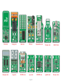
1
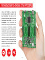
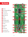
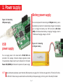
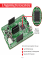
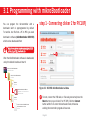
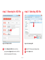
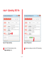
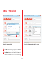
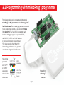
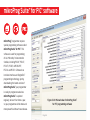
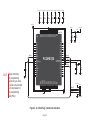
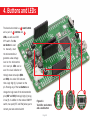
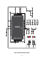
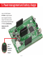
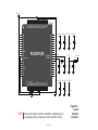
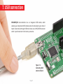
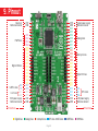
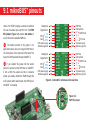
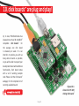
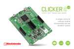
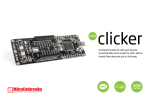
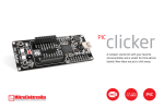
A compact starter kit
with your favorite
microcontroller and two
mikroBUS™ sockets
TO OUR VALUED CUSTOMERS
I want to express my thanks to you for being interested in our products and for having
confidence in MikroElektronika.
The primary aim of our company is to design and produce high quality electronic products
and to constantly improve the performance thereof in order to better suit your needs.
Nebojsa Matic
General Manager
The PIC® and Windows® logos and product names are trademarks of Microchip Technology® and Microsoft® in the U.S.A. and other countries.
Page 2
Table of contents
Introduction to clicker 2 for PIC18FJ
4
Key features
5
1. Power supply
7
4. Buttons and LEDs
18
2. PIC18F87J50 microcontroller
9
5. Power management and battery charger
20
9
6. Oscillators
21
Key microcontroller features
3.2 Programming with mikroProg™ programmer
mikroProg Suite for PIC software
™
®
15
16
3. Programming the microcontroller
10
7. USB connection
23
3.1 Programming with mikroBootloader
11
8. Pads
25
step 1 – Connecting clicker 2 for PIC18FJ 11
9. Pinout
26
step 2 – Browsing for .HEX file 12
9.1 mikroBUS™ pinout
27
step 3 – Selecting .HEX file 12
™
10. click boards are plug and play!
28
step 4 – Uploading .HEX file
13
11. Dimensions
30
step 5 – Finish upload
14
Page 3
Introduction to clicker 2 for PIC18FJ
clicker 2 for PIC18FJ is a compact dev.
kit with two mikroBUS™ sockets for click
board connectivity. You can use it to
quickly build your own gadgets with unique
functionalities and features. It carries the
PIC18F87J50, a 8-bit microcontroller, two
indication LEDs, two general purpose buttons,
a reset button, an on/off switch, a li-polymer
battery connector, a USB Mini-B connector and
two mikroBUS™ sockets. A mikroProg connector
and a 2x26 pinout for interfacing with external
electronics are also provided. The mikroBUS™
connector consists of two 1x8 female headers
with SPI, I2C, UART, RST, PWM, Analog and
Interrupt lines as well as 3.3V, 5V and GND
power lines. clicker 2 for PIC18FJ board can be
powered over a USB cable.
Page 4
Key features
1
10
2
11
1 ON/OFF switch
2 Pads for connecting external ON/OFF switch
3 8 MHz crystal oscillator
12
3
13
4 two 1x26 connection pads
5 mikroBUS™ sockets 1 and 2
6 Pushbuttons
7 Additional LEDs
8 LTC3586 USB power manager IC
4
4
5
5
6
6
7
7
8
14
9
15
9 Power and Charge indication LEDs
10 RESET button
11 USB mini-B connector
12 PIC18F87J50
13 PWM selection jumper
14 Li-Polymer battery connector
15 mikroProg™ programmer connector
Page 5
C9
C10
C11
C12
C33
100nF
100nF
VCC-3.3V VCC-3.3V VCC-3.3V
100nF
100nF
100nF
VCC-3.3V
10uF
VCC-3.3V
R16
C14
C15
C16
C17
10K
22uF
1uF
10nF
1uF
VSYS
R23
1K69
2.2uF
L2
L3
2.2uH
VCC-USB
LDO3V3
C32
R19
324K
22uF
10uF
VCC-5V VCC-5V VCC-5V
R27
16K9
C21
C24
RF7-GPIO
RF6-VSENSE
RF5-AN10
USB-D_P
R28
USB-D_N
R29
RF2-AN7
RH7-AN15
RH6-AN14
PIC18F87J50
RJ2
RJ3
RB0
RB1
RB2
RB3
RB4
RB5
RB6
GND
CLKO/RA6/OSC2
CLKI/RA7/OSC1
VCC
RB7
RC5
RC4
RC3
RC2
RJ7
RJ6
60
59
58
57
56
55
54
53
52
51
50
49
48
47
46
45
44
43
42
41
R22
105K
RJ2-GPIO
RJ3-GPIO
RB0-INT0
RB1-INT1
RB2-MB2_INT2
RB3-MB1_INT3
RB4-GPIO
RB5-GPIO
RB6-PGC
VCC-5V
VCC-5V
C29
C30
C27
C28
22uF
1uF
10nF
1
AVCC
VCC-3.3V
LD3
RG3-MB1_PWM4
RB3-MB1_INT3
RG2-UART2_RX
RG1-UART2_TX
RD6-I2C2_SCL
RD5-I2C2_SDA
PWM
INT
RX
TX
SCL
SDA
5V
GND
RA1-MB2_AN1
RD0-MB2_RST
RD1-MB2_CS
RC3-SPI1_SCK
RC4-SPI1_MISO
RC5-SPI1_MOSI
AN
RST
CS
SCK
MISO
MOSI
3.3V
GND
RE7-GPIO
MB2_PWM
RG0-PWM3
2
HDR1
MB2_PWM
RB2-MB2_INT2
RC7-UART1_RX
RC6-UART1_TX
RD6-I2C2_SCL
RD5-I2C2_SDA
PWM
INT
RX
TX
SCL
SDA
5V
GND
VCC-3.3V
RB7-PGD
RC5-SPI1_MOSI
RC4-SPI1_MISO
RC3-SPI1_SCK
R9
RC2-PWM1
RJ7-GPIO
RJ6-GPIO
8MHz
C5
22pF
R7
AVCC
VCC-3.3V
FP1
C6
22pF
C1
100nF
R3
10K
R4
RESET#
R2
2K2
AN
HD1
1
2
3
4
5
VCC-3.3V
R5
10K
VCC-3.3V
VCC-BAT
R10
1M
RE5-SENSEL
VCC-USB
T3
VCC-3.3V
RX
TX
SCL
SDA
VCC-BAT
mPROG
R6
10K
RE2-GPIO
USB-D_N
USB-D_P
R24 10K
DMP2305U
CN2
FP2
FERRITE
C26
R25
1M
M1
R11
1K
T2
PWM
INT
SCK
SDI
SDO
RESET#
RC1-PWM2
RC2-PWM1
RG4-PWM5
RG0-PWM3
RH0-GPIO
RA4-GPIO
RJ7-GPIO
RJ6-GPIO
RJ4-GPIO
RB5-GPIO
RB4-GPIO
RJ2-GPIO
RJ3-GPIO
RA5-GPIO
RJ0-GPIO
RJ1-GPIO
RC7-UART1_RX
RC6-UART1_TX
RD6-I2C2_SCL
RD5-I2C2_SDA
C3
100nF
VCC-3.3V
2K2
HDR2
T1
C2
2.2uF
R1
RA2-AN2
RH5-AN13
RH4-AN12
RH6-AN14
RH7-AN15
RF2-AN7
RF5-AN10
RB0-INT0
RB1-INT1
RB2-MB2_INT2
RB3-MB1_INT3
RA3-GPIO
RE0-GPIO
RH2-GPIO
RE1-GPIO
RH1-GPIO
RC0-GPIO
RE3-GPIO
RF7-GPIO
RC3-SPI1_SCK
RC4-SPI1_MISO
RC5-SPI1_MOSI
VCC-3.3V
2K2
RB6-PGC
RB7-PGD
RESET#
clicker 2 for PIC18FJ schematic
Page 6
VCC-5V
X1
R8
470
VSYS
VCC-3.3V
J1
OSC2
OSC1
300pF
10pF
AN
RST
CS
SCK
MISO
MOSI
3.3V
GND
33pF
10pF
R21
R26
88K7
VCC-3.3V VCC-3.3V
2.2uH
C23
C4
10uF
VCC-3.3V
15K
C31
RH1
RH0
RE2
RE3
RE4
RE5
RE6
RE7
RD0
VCC
GND
RD1
RD2
RD3
RD4
RD5
RD6
RD7
RJ0
RJ1
PWR-EN
VCC-5V
C25
100nF
VCC-USB
2.2uF
RH2
RH3
RE1
RE0
RG0
RG1
RG2
RG3
MCLR
RG4
GND
VCCcore/Vcap
RF7
RF6
RF5
RF4/D+
RF3/DRF2
RH7
RH6
RD4-LD1
VCC-3.3V
R17
1M
1
2
3
4
5
6
7
8
9
10
11
12
13
14
15
16
17
18
19
20
RA5-GPIO
RA4-GPIO
RC1-PWM2
RC0-GPIO
RC6-UART1_TX
RC7-UART1_RX
RJ4-GPIO
RJ5-STAT
10K
19
18
17
16
15
14
13
C20
RH2-GPIO
RH3-T3
RE1-GPIO
RE0-GPIO
RG0-PWM3
RG1-UART2_TX
RG2-UART2_RX
RG3-MB1_PWM4
RESET#
RG4-PWM5
VCC-5V
RH5
RH4
VUSB
VBAT
AVCC
AGND
RA3
RA2
RA1
RA0
GND
VCC
RA5
RA4
RC1
RC0
RC6
RC7
RJ4
RJ5
R20
C22
22uF
LTC3586
SWCD3
EN3
VOUT3
VOUT3
VIN3
VIN3
SWAB3
100nF
VSYS
C19
RA0-MB1_AN0
RD2-MB1_RST
RD3-MB1_CS
RC3-SPI1_SCK
RC4-SPI1_MISO
RC5-SPI1_MOSI
U1
PIC18F87J50
21
22
23
24
25
26
27
28
29
30
31
32
33
34
35
36
37
38
39
40
RE6-FAULT
GATE
CHRG#
PROG
FB1
VIN1
SW1
SW2
VIN2
FB2
VIN4
EN1
EN2
31
30
29
28
27
26
25
24
23
22
21
20
3.3uH
BAT
EN4
VOUT
VBUS
VBUS
SW
FAULT#
ILIM0
ILIM1
LDO3V3
CLPROG
NTC
VOUT4
VOUT4
SW4
MODE
FB4
FB3
VC3
VCC-USB
L1
U2
LTC3586
1
2
3
4
5
6
7
8
9
10
11
12
VSYS
32
33
34
35
36
37
38
PWR-EN
C18
1
3K3
VCC-BAT
2
R18
M2
DMP2305U
PWR-EN
3
RA3-GPIO
RA2-AN2
RA1-MB2_AN1
RA0-MB1_AN0
2K2
RJ5-STAT
SW1
LDO3V3
JS202011AQN
LDO3V3 VCC-3.3V VCC-3.3V VCC-3.3V LDO3V3
LD4B
RED
R15
RH5-AN13
RH4-AN12
LDO3V3
VSYS
VCC-3.3V
RE4-LD2
VCC-3.3V
C8
10uF
RH3-T3
VCC-3.3V
C7
80
79
78
77
76
75
74
73
72
71
70
69
68
67
66
65
64
63
62
61
VCC-3.3V
RD7-T2
CN1
BATT CONN
RD1-MB2_CS
RD2-MB1_RST
RD3-MB1_CS
RD4-LD1
RD5-I2C2_SDA
RD6-I2C2_SCL
RD7-T2
RJ0-GPIO
RJ1-GPIO
C34
2.2uF
RH1-GPIO
RH0-GPIO
RE2-GPIO
RE3-GPIO
RE4-LD2
RE5-SENSEL
RE6-FAULT
RE7-GPIO
RD0-MB2_RST
VCC-BAT
VCC-BAT
1
2
3
4
5
VBUS
DD+
ID
GND
10nF
USB MINIB
R12
100K
R13
100K
RF6-VSENSE
C13
100nF
R14
100K
1. Power supply
Battery power supply
Figure 1-1: Connecting
USB power supply
You can also power the board using a Li-Polymer battery, via onboard battery connector. On-board battery charger circuit enables
you to charge the battery over USB connection. LED diode
(RED) will indicate when battery is charging. Charging current is
~300mA and charging voltage is 4.2V DC.
USB
power supply
Figure 1-2: Connecting
Li-Polymer battery
You can supply power to the board with a Mini-B USB cable
provided in the package. On-board voltage regulators provide
the appropriate voltage levels to each component on the board.
Power LED (GREEN) will indicate the presence of power supply.
NOTE Some click boards need more current than the USB connection can supply. For 3.3V clicks, the upper limit is 750 mA; for 5V clicks,
it’s 500 mA. In those cases you would need to use the battery as the power supply, or the vsys pin on the side of the board.
Page 7
LDO3V3
2K2
RJ5-STAT
R16
C14
C15
C16
C17
10K
22uF
1uF
10nF
1uF
3K3
VSYS
L1
3.3uH
RE6-FAULT
R20
C22
10K
22uF
GATE
CHRG#
PROG
FB1
VIN1
SW1
SW2
VIN2
FB2
VIN4
EN1
EN2
31
30
29
28
27
26
25
24
23
22
21
20
VCC-USB
BAT
EN4
VOUT
VBUS
VBUS
SW
FAULT#
VCC-3.3V
R23
1K69
LTC3586
VCC-USB
LDO3V3
C31
C32
22uF
10uF
VCC-3.3V VCC-3.3V VCC-3.3V
C10
C11
C12
VCC-3.3V
C33
10uF
100nF
100nF
100nF
100nF
100nF
10uF
AVCC
L2
2.2uH
C23
10pF
VCC-3.3V
FP1
PWR-EN
C18
100nF
R17
1M
VCC-BAT
VCC-BAT
PWR-EN
VCC-BAT
C34
VCC-3.3V
VCC-3.3V VCC-3.3V
R19
324K
VCC-5V VCC-5V VCC-5V
R27
16K9
C9
VCC-BAT
R10
1M
19
18
17
16
15
14
13
R21
R26
88K7
VCC-3.3V
C8
C1
100nF
C2
2.2uF
VSYS
C20
2.2uF
15K
L3
2.2uH
VCC-3.3V
C7
VSYS
C19
2.2uF
VCC-5V
C25
100nF
VCC-USB
SWCD3
EN3
VOUT3
VOUT3
VIN3
VIN3
SWAB3
ILIM0
ILIM1
LDO3V3
CLPROG
NTC
VOUT4
VOUT4
SW4
MODE
FB4
FB3
VC3
VSYS
32
33
34
35
36
37
38
U2
LTC3586
1
2
3
4
5
6
7
8
9
10
11
12
PWR-EN
2
1
DMP2305U
VCC-3.3V
3
R18
M2
VCC-BAT
SW1
LDO3V3
JS202011AQN
LDO3V3 VCC-3.3V VCC-3.3V VCC-3.3V LDO3V3
LD4B
RED
R15
C24
2.2uF
C21
HDR2
R11
1K
DMP2305U
R12
100K
AN
PWM
R13
100K
33pF
RF6-VSENSE
INT
C13
100nF
R22
105K
300pF
VCC-5V
RE5-SENSEL
CN1
BATT CONN
HDR1
M1
R14
100K
VCC-USB
VCC-5V
C29
C30
C27
C28
10pF
22uF
1uF
10nF
CN2
FP2
FERRITE
VCC-3.3V
LD3
C26
R8
470
1
2
3
4
5
VBUS
DD+
ID
GND
10nF
USB MINIB
VSYS
Figure 1-3: Power supply schematic
Page 8
VCC-3.3V
SCK
SDI
SDO
RX
TX
SCL
SDA
VCC-3.3V
2. PIC18F87J50 microcontroller
The clicker 2 for PIC18FJ development tool comes with the
PIC18F87J50 device. This 8-bit low power high performance
microcontroller is rich with on-chip peripherals and features
128 KB of program memory and 3094 bytes of RAM. It has
integrated full speed USB 2.0. support.
12 MIPS 8bit Core
- nanoWatt
- 48MHz
31 Level
Stack
PIC18FJ
Program
Counter
Instruction
Data
Addresse Addre
ss
Decode
Data
Data/Memor
Key microcontroller features
y Bus
Flash
(Up to 128K
- Up to 12 MIPS operation
B)
RAM
(Up to 3.9K
B)
- 8-bit architecture
VREG
Data Bus
- 128 KB of program memory
- 3,904 bytes of RAM
USB PMP
Timers
- 65 I/O pins
- Internal oscillator 8 MHz, 32 Khz
- 2-UART, 2-SPI, 2-I C, USB 2.0, DAC, ADC etc.
2
Page 9
Comparators
ADC
10-Bit
EUSART
CCP
MSSP
3. Programming the microcontroller
Figure 3-1:
PIC18F87J50
microcontroller
The microcontroller can be programmed in three ways:
01 Using USB HID mikroBootloader,
02 Using external mikroProg™ for PIC18FJ programmer
03 Using external ICD2/3® programmer
Page 10
3.1 Programming with mikroBootloader
You can program the microcontroller with a
bootloader which is preprogrammed by default.
To transfer .hex file from a PC to MCU you need
bootloader software (mikroBootloader USB HID)
which can be downloaded from:
step 1 – Connecting clicker 2 for PIC18FJ
http://www.mikroe.com/downloads/get/2156/
clicker_2_pic18fj_bootloader.zip
01
After the mikroBootloader software is downloaded,
unzip it to desired location and start it.
clicker 2 for PIC18FJ Bootloader
WinRAR ZIP archive
clicker 2 for PIC18FJ Bootloader
File folder
Software
File folder
mikroBootloader USB HID.exe
Bootloader tool for mikroElektron...
mikroElektronika
Firmware
File folder
clicker 2 for PIC18FJ P18F87J50 USB
HID Bootloader v1.300.hex
HEX File
Figure 3-2: USB HID mikroBootloader window
01 To start, connect the USB cable, or if already connected press the
Reset button on your clicker 2 for PIC18FJ. Click the Connect
button within 5s to enter the bootloader mode, otherwise
existing microcontroller program will execute.
Page 11
step 2 – Browsing for .HEX file
step 3 – Selecting .HEX file
01
01
02
Figure 3-3: Browse for HEX
Figure 3-4: Selecting HEX
01 Click the Browse for HEX button and from a
01 Select .HEX file using open dialog window.
pop-up window (Figure 3.4) choose the .HEX file
02 Click the Open button.
which will be uploaded to MCU memory.
Page 12
step 4 – Uploading .HEX file
01
01
Figure 3-5: Begin uploading
Figure 3-6: Progress bar
01 To start .HEX file bootloading click the
Begin uploading button.
01 Progress bar enables you to monitor .HEX file uploading.
Page 13
step 5 – Finish upload
01
Figure 3-7: Restarting MCU
Figure 3-8: mikroBootloader ready for next job
01 Click OK button after the uploading process is finished.
02 Press Reset button on clicker 2 for PIC18FJ board and
wait for 5 seconds. Your program will run automatically.
Page 14
3.2 Programming with mikroProg™ programmer
The microcontroller can be programmed with external
mikroProg™ for PIC programmer and mikroProg Suite™
GND
MCLR#
PGD
PGC
VCC 3.3V
You can also
program it
with ICD2®
or ICD3® if
you reroute
the wires like
shown here.
1. NC
2. PGC
3. PGD
4. GND
5. VCC 3.3V
6. MCLR#
for PIC® software. The external programmer is connected
to the development system via 1x5 connector Figure
3-9. mikroProg™ is a fast USB 2.0 programmer with
hardware debugger support. It supports PIC10®,
dsPIC30/33®, PIC24® and PIC32® devices
in a single programmer. It supports over
570 microcontrollers from Microchip®.
Outstanding performance, easy operation
and elegant design are its key features.
ICD2/3
programmer
clicker 2 for
PIC18FJ 1x5
programming
headers
Figure 3-9:
mikroProg™
connector
Page 15
mikroProg Suite™ for PIC® software
mikroProg™ programmer requires
special programming software called
mikroProg Suite™ for PIC®. This
software is used for programming
of ALL Microchip® microcontroller
families, including PIC10®, PIC12®,
PIC16®, PIC18®, dsPIC30/33®,
PIC24® and PIC32®. Software has
intuitive interface and SingleClick™
programming technology. Just by
downloading the latest version of
mikroProg Suite™ your programmer
is ready to program new devices.
mikroProg Suite™ is updated
regularly, at least four times a year,
so your programmer will be more and
more powerful with each new release.
Figure 3-10: Main window of mikroProg Suite™
for PIC® programming software
Page 16
VCC-3.3V
VCC-3.3V
VCC-3.3V
C7
C8
C9
VCC-3.3V VCC-3.3V VCC-3.3V
C10
C11
C12
VCC-3.3V
C33
10uF
100nF
100nF
100nF
100nF
100nF
10uF
VCC-3.3V
10uF
NOTE Before attaching
the programming
connector, you have
to solder the provided
1x5 male header to
the programming
pads (HD1).
PIC18F87J50
RJ2
RJ3
RB0
RB1
RB2
RB3
RB4
RB5
RB6
GND
CLKO/RA6/OSC2
CLKI/RA7/OSC1
VCC
RB7
RC5
RC4
RC3
RC2
RJ7
RJ6
21
22
23
24
25
26
27
28
29
30
31
32
33
34
35
36
37
38
39
40
C4
RH2
RH3
RE1
RE0
RG0
RG1
RG2
RG3
MCLR
RG4
GND
VCCcore/Vcap
RF7
RF6
RF5
RF4/D+
RF3/DRF2
RH7
RH6
C1
100nF
60
59
58
57
56
55
54
53
52
51
50
49
48
47
46
45
44
43
42
41
AVCC
C2
2.2uF
RB6-PGC
OSC2
OSC1
X1
RB7-PGD
8MHz
C5
22pF
RH5
RH4
VUSB
VBAT
AVCC
AGND
RA3
RA2
RA1
RA0
GND
VCC
RA5
RA4
RC1
RC0
RC6
RC7
RJ4
RJ5
RESET#
1
2
3
4
5
6
7
8
9
10
11
12
13
14
15
16
17
18
19
20
VCC-3.3V
FP1
RH1
RH0
RE2
RE3
RE4
RE5
RE6
RE7
RD0
VCC
GND
RD1
RD2
RD3
RD4
RD5
RD6
RD7
RJ0
RJ1
80
79
78
77
76
75
74
73
72
71
70
69
68
67
66
65
64
63
62
61
AVCC
U1
PIC18F87J50
VCC-3.3V
RB6-PGC
RB7-PGD
RESET#
C6
22pF
HD1
1
2
3
4
5
mPROG
Figure 3-11: mikroProg™ connection schematic
Page 17
4. Buttons and LEDs
The board also contains a 01 reset button
and a pair of 02 buttons and 03
LEDs, as well as an ON/
OFF switch. The Reset button is used
to manually reset
the microcontroller—it
generates a low voltage
level on the microcontroller’s reset pin. LEDs can be
used for visual indication of
the logic state on two pins (RD4
and RE4). An active LED indicates
that a logic high (1) is present on the
pin. Pressing any of the two buttons can
change the logic state of the microcontroller
pins (RD7 and RH3) from logic high (1) to logic low (0). In addition to the onboard ON/OFF
switch, two pads (EXT and PSW) allow you to
connect your own external switch.
03
Figure 4-1:
Two LEDs, two buttons
and a reset button
Page 18
02
01
RD7-T2
RD4-LD1
RE4-LD2
VCC-3.3V
RESET#
R3
10K
R4
2K2
VCC-3.3V
T1
100nF
RH1
RH0
RE2
RE3
RE4
RE5
RE6
RE7
RD0
VCC
GND
RD1
RD2
RD3
RD4
RD5
RD6
RD7
RJ0
RJ1
80
79
78
77
76
75
74
73
72
71
70
69
68
67
66
65
64
63
62
61
C3
U1
PIC18F87J50
60
59
58
57
56
55
54
53
52
51
50
49
48
47
46
45
44
43
42
41
VCC-3.3V
OSC2
OSC1
VCC-3.3V VCC-3.3V VCC-3.3V VCC-3.3V VCC-3.3V VCC-3.3V
C7
C8
C9
C10
C11
C12
C33
10uF
100nF
100nF
100nF
100nF
100nF
10uF
AVCC
VCC-3.3V
FP1
X1
8MHz
C5
22pF
C1
100nF
C6
22pF
C2
2.2uF
R1
R2
2K2
2K2
T2
VCC-3.3V
R5
10K
T3
VCC-3.3V
R6
10K
Figure 4-2: Other modules connection schematic
Page 19
RE4-LD2
RH3-T3
AVCC
RD7-T2
10uF
PIC18F87J50
RJ2
RJ3
RB0
RB1
RB2
RB3
RB4
RB5
RB6
GND
CLKO/RA6/OSC2
CLKI/RA7/OSC1
VCC
RB7
RC5
RC4
RC3
RC2
RJ7
RJ6
RD4-LD1
C4
RH2
RH3
RE1
RE0
RG0
RG1
RG2
RG3
MCLR
RG4
GND
VCCcore/Vcap
RF7
RF6
RF5
RF4/D+
RF3/DRF2
RH7
RH6
RH5
RH4
VUSB
VBAT
AVCC
AGND
RA3
RA2
RA1
RA0
GND
VCC
RA5
RA4
RC1
RC0
RC6
RC7
RJ4
RJ5
RESET#
1
2
3
4
5
6
7
8
9
10
11
12
13
14
15
16
17
18
19
20
21
22
23
24
25
26
27
28
29
30
31
32
33
34
35
36
37
38
39
40
RH3-T3
5. Power management and battery charger
clicker 2 for PIC18FJ features
LTC®3586-2, a highly integrated
power management and battery
charger IC that includes a current
limited switching PowerPath manager.
LTC®3586 also enables battery
charging over a USB
connection.
Figure 5-1:
power
management
and battery
charger IC
Page 20
6. Oscillators
Board is equipped
with 8MHz crystal
oscillator (X1) circuit
that provides external clock
waveform to the microcontroller
CLKO and CLKI pins. This base
frequency is suitable for further clock
multipliers and ideal for generation of
necessary USB clock, which ensures proper
operation of bootloader and your custom
USB-based applications.
Figure 6-1:
8MHz crystal
oscillator
module (X1)
Page 21
U1
PIC18F87J50
RH1
RH0
RE2
RE3
RE4
RE5
RE6
RE7
RD0
VCC
GND
RD1
RD2
RD3
RD4
RD5
RD6
RD7
RJ0
RJ1
80
79
78
77
76
75
74
73
72
71
70
69
68
67
66
65
64
63
62
61
VCC-3.3V
RH2
RH3
RE1
RE0
RG0
RG1
RG2
RG3
MCLR
RG4
GND
VCCcore/Vcap
RF7
RF6
RF5
RF4/D+
RF3/DRF2
RH7
RH6
PIC18F87J50
RJ2
RJ3
RB0
RB1
RB2
RB3
RB4
RB5
RB6
GND
CLKO/RA6/OSC2
CLKI/RA7/OSC1
VCC
RB7
RC5
RC4
RC3
RC2
RJ7
RJ6
21
22
23
24
25
26
27
28
29
30
31
32
33
34
35
36
37
38
39
40
RH5
RH4
VUSB
VBAT
AVCC
AGND
RA3
RA2
RA1
RA0
GND
VCC
RA5
RA4
RC1
RC0
RC6
RC7
RJ4
RJ5
1
2
3
4
5
6
7
8
9
10
11
12
13
14
15
16
17
18
19
20
60
59
58
57
56
55
54
53
52
51
50
49
48
47
46
45
44
43
42
41
VCC-3.3V
OSC2
OSC1
VCC-3.3V
VCC-3.3V
VCC-3.3V
C9
C10
C7
C8
100nF
100nF
10uF
100nF
AVCC
X1
8MHz
C5
22pF
VCC-3.3V
VCC-3.3V
FP1
C6
22pF
VCC-3.3V
C1
100nF
C2
2.2uF
VCC-3.3V
C11
C12
C33
100nF
100nF
10uF
AVCC
NOTE The use of crystal in all other schematics is implied even if
it is purposely left out, because of the schematics clarity.
Page 22
Figure 6-2:
Crystal
oscillator
schematic
7. USB connection
PIC18F87J50 microcontrollers has an integrated USB module, which
enables you to implement USB communication functionality to your clicker 2
board. Connection with target USB host is done over a Mini-B USB connector
which is positioned next to the battery connector.
Figure 7-1:
Connecting USB
cable to clicker 2
Page 23
RE2-GPIO
VCC-USB
U1
PIC18F87J50
RE2-GPIO
USB-D_N
USB-D_P
RH1
RH0
RE2
RE3
RE4
RE5
RE6
RE7
RD0
VCC
GND
RD1
RD2
RD3
RD4
RD5
RD6
RD7
RJ0
RJ1
80
79
78
77
76
75
74
73
72
71
70
69
68
67
66
65
64
63
62
61
VCC-3.3V
CN2
FP2
FERRITE
R24 10K
1
2
3
4
5
C26
USB-D_P
R28
USB-D_N
R29
PIC18F87J50
RJ2
RJ3
RB0
RB1
RB2
RB3
RB4
RB5
RB6
GND
CLKO/RA6/OSC2
CLKI/RA7/OSC1
VCC
RB7
RC5
RC4
RC3
RC2
RJ7
RJ6
RH5
RH4
VUSB
VBAT
AVCC
AGND
RA3
RA2
RA1
RA0
GND
VCC
RA5
RA4
RC1
RC0
RC6
RC7
RJ4
RJ5
10uF
RH2
RH3
RE1
RE0
RG0
RG1
RG2
RG3
MCLR
RG4
GND
VCCcore/Vcap
RF7
RF6
RF5
RF4/D+
RF3/DRF2
RH7
RH6
21
22
23
24
25
26
27
28
29
30
31
32
33
34
35
36
37
38
39
40
C4
1
2
3
4
5
6
7
8
9
10
11
12
13
14
15
16
17
18
19
20
60
59
58
57
56
55
54
53
52
51
50
49
48
47
46
45
44
43
42
41
R25
1M
OSC2
OSC1
10nF
USB MINIB
AVCC
VCC-3.3V
X1
FP1
8MHz
C5
22pF
C1
100nF
C6
22pF
C2
2.2uF
VCC-3.3V
VCC-3.3V
VCC-3.3V
C7
C8
C9
C10
C11
C12
C33
10uF
100nF
100nF
100nF
100nF
100nF
10uF
AVCC
Figure 7-2: USB module connection schematic
Page 24
VBUS
DD+
ID
GND
VCC-3.3V VCC-3.3V VCC-3.3V
VCC-3.3V
HDR2
RJ0-GPIO
RJ1-GPIO
RE3-GPIO
RH1-GPIO
RH0-GPIO
VSYS HDR1
RA2-AN2
RH5-AN13
RH4-AN12
RH6-AN14
RH7-AN15
RF2-AN7
RF5-AN10
RB0-INT0
RB1-INT1
RB2-MB2_INT2
RB3-MB1_INT3
RA3-GPIO
RE0-GPIO
RH2-GPIO
RE1-GPIO
RH1-GPIO
RC0-GPIO
RE3-GPIO
RF7-GPIO
RC3-SPI1_SCK
RC4-SPI1_MISO
RC5-SPI1_MOSI
RD5-I2C2_SDA
RD6-I2C2_SCL
8. Pads
AN
RESET#
RC1-PWM2
RC2-PWM1
RG4-PWM5
RG0-PWM3
RH0-GPIO
RA4-GPIO
RJ7-GPIO
RJ6-GPIO
RJ4-GPIO
RB5-GPIO
RB4-GPIO
RJ2-GPIO
RJ3-GPIO
RA5-GPIO
RJ0-GPIO
RJ1-GPIO
RC7-UART1_RX
RC6-UART1_TX
RD6-I2C2_SCL
RD5-I2C2_SDA
PWM
VCC-3.3V
U1
PIC18F87J50
RH1
RH0
RE2
RE3
RE4
RE5
RE6
RE7
RD0
VCC
GND
RD1
RD2
RD3
RD4
RD5
RD6
RD7
RJ0
RJ1
80
79
78
77
76
75
74
73
72
71
70
69
68
67
66
65
64
63
62
61
INT
RH2-GPIO
SCK
SDI
SDO
VCC-3.3V
RE1-GPIO
RE0-GPIO
RG0-PWM3
RESET#
RG4-PWM5
RF7-GPIO
C4
RF5-AN10
RF2-AN7
RH7-AN15
RH6-AN14
RH2
RH3
RE1
RE0
RG0
RG1
RG2
RG3
MCLR
RG4
GND
VCCcore/Vcap
RF7
RF6
RF5
RF4/D+
RF3/DRF2
RH7
RH6
PIC18F87J50
RJ2
RJ3
RB0
RB1
RB2
RB3
RB4
RB5
RB6
GND
CLKO/RA6/OSC2
CLKI/RA7/OSC1
VCC
RB7
RC5
RC4
RC3
RC2
RJ7
RJ6
60
59
58
57
56
55
54
53
52
51
50
49
48
47
46
45
44
43
42
41
RJ2-GPIO
RJ3-GPIO
RB0-INT0
RB1-INT1
RB2-MB2_INT2
RB3-MB1_INT3
RB4-GPIO
RB5-GPIO
RX
TX
SCL
SDA
VCC-3.3V
OSC2
OSC1
X1
R7
R9
RC5-SPI1_MOSI
RC4-SPI1_MISO
RC3-SPI1_SCK
RC2-PWM1
RJ7-GPIO
RJ6-GPIO
8MHz
C5
C6
22pF
22pF
C2
2.2uF
AVCC
RH5-AN13
RH4-AN12
C1
100nF
Pads HDR2
RA5-GPIO
RA4-GPIO
RC1-PWM2
RC0-GPIO
RC6-UART1_TX
RC7-UART1_RX
RJ4-GPIO
RJ5-STAT
VCC-3.3V
FP1
RA3-GPIO
RA2-AN2
RA1-MB2_AN1
RA0-MB1_AN0
AVCC
21
22
23
24
25
26
27
28
29
30
31
32
33
34
35
36
37
38
39
40
RH5
RH4
VUSB
VBAT
AVCC
AGND
RA3
RA2
RA1
RA0
GND
VCC
RA5
RA4
RC1
RC0
RC6
RC7
RJ4
RJ5
10uF
1
2
3
4
5
6
7
8
9
10
11
12
13
14
15
16
17
18
19
20
VCC-3.3V VCC-3.3V VCC-3.3V VCC-3.3V VCC-3.3V VCC-3.3V
VCC-3.3V
C7
C8
C9
C10
C11
C12
C33
10uF
100nF
100nF
100nF
100nF
100nF
10uF
Figure 8-1: Connecting pads schematic
Pads HDR1
Most microcontroller pins are available for further connectivity via two 1x26 rows of connection
pads on both sides of the clicker 2 for PIC18FJ board. They are designed to match additional
shields, such as Battery Boost shield, Gaming, PROTO shield and others.
Page 25
9. Pinout
Reset pin
Reference Ground
PWM lines
Digital I/O lines
RX
TX
SCL
I2C2 Lines
SDA
3.3V power supply
Reference Ground
UART1 Lines
RST
GND
VSYS
GND
RA2
RH5
RH4
RH6
RH7
RF2
RF5
RB1
RB0
RB2
RB3
RA3
RE0
RH2
RE1
RH1
RC0
RE3
RF7
RC3
RC4
RC5
3.3V
GND
RC1
RC2
RG4
RG0
RH0
RA4
RJ7
RJ6
RJ4
RB5
RB4
RJ2
RJ3
RA5
RJ0
RJ1
RC7
RC6
RD6
RD5
3.3V
GND
Pin functions
Digital lines
System power supply
Reference Ground
Analog Lines
Interrupt Lines
Digital I/O lines
SCK
SDI
SPI1 Lines
SDO
3.3V power supply
Reference Ground
Pin functions
Analog Lines
Interrupt Lines
SPI Lines
Page 26
I2C Lines
UART lines
PWM lines
9.1 mikroBUS™ pinouts
clicker 2 for PIC18FJ employs a solution to optimize
the use of available pins and MCU I/Os. The PWM
SEL jumper (Figure 9-2) enables two modes of
use for the second available PWM line:
1 The default position of the jumper is for
applications when you’re not using the PWM line on
the 1x26 pinout on the right side of the board. This
keeps this PWM available through mikroBUS™ 2
If you resolder the jumper into the second
position, it would turn the PWM line on mikroBUS™
2 into a GPIO. You would use this in scenarios
where you already utilized the PWM through the
1x26 pinout (which would make the PWM pin on
mikroBUS™ 2 unusable)
2
Analog line
Digital lines*
SCK
MISO
MOSI
3.3V power supply
Reference ground
SPI1
lines
Analog line
Digital lines*
SCK
MISO
MOSI
3.3V power supply
Reference ground
SPI1
lines
RA0
RD2
RD3
RC3
RC4
RC5
3.3V
GND
RG3
RB3
RG2
RG1
RD6
RD5
5V
GND
PWM line
Interrupt line
RX
TX UART2 lines
SCL
I2C2 lines
SDA
5V power supply
Reference ground
RA1
RD0
RD1
RC3
RC4
RC5
3.3V
GND
RG0
RB2
RC7
RC6
RD6
RD5
5V
RD5
PWM line
Interrupt line
RX
TX UART1 lines
SCL
I2C2 lines
SDA
5V power supply
Reference ground
Figure 9-1: mikroBUS™ individual and shared lines
Figure 9-2:
PWM SEL jumper
Page 27
10. click boards™ are plug and play!
Up to now, MikroElektronika has
released more than 90 mikroBUS™
compatible click boards™. On
the average, one click board
is released per week. It is our
intention to provide you with as
many add-on boards as possible,
so you will be able to expand your
development board with additional
functionality. Each board comes
with a set of working example
code. Please visit the click boards™
webpage for the complete list of
currently available boards:
Figure 10-1:
clicker 2 for PIC18FJ
driving click boards™
www.mikroe.com/click
Page 28
RFid click
Relay click
8x8 click
BarGraph click
7seg click
THERMO click
FM click
Gyro click
Page 29
Bluetooth2 click
Thunder click
USB SPI click
EEPROM click
LightHz click
Pressure click
11. Dimensions
Page 30
DISCLAIMER
All the products owned by MikroElektronika are protected by copyright law and international copyright treaty. Therefore, this manual is to be treated as any
other copyright material. No part of this manual, including product and software described herein, may be reproduced, stored in a retrieval system, translated
or transmitted in any form or by any means, without the prior written permission of MikroElektronika. The manual PDF edition can be printed for private or
local use, but not for distribution. Any modification of this manual is prohibited.
MikroElektronika provides this manual ‘as is’ without warranty of any kind, either expressed or implied, including, but not limited to, the implied warranties
or conditions of merchantability or fitness for a particular purpose.
MikroElektronika shall assume no responsibility or liability for any errors, omissions and inaccuracies that may appear in this manual. In no event shall
MikroElektronika, its directors, officers, employees or distributors be liable for any indirect, specific, incidental or consequential damages (including damages
for loss of business profits and business information, business interruption or any other pecuniary loss) arising out of the use of this manual or product,
even if MikroElektronika has been advised of the possibility of such damages. MikroElektronika reserves the right to change information contained in this
manual at any time without prior notice, if necessary.
HIGH RISK ACTIVITIES
The products of MikroElektronika are not fault – tolerant nor designed, manufactured or intended for use or resale as on – line control equipment
in hazardous environments requiring fail – safe performance, such as in the operation of nuclear facilities, aircraft navigation or communication
systems, air traffic control, direct life support machines or weapons systems in which the failure of Software could lead directly to death, personal
injury or severe physical or environmental damage (‘High Risk Activities’). MikroElektronika and its suppliers specifically disclaim any expressed or
implied warranty of fitness for High Risk Activities.
TRADEMARKS
The MikroElektronika name and logo, mikroC™, mikroBasic™, mikroPascal™, Visual TFT™, Visual GLCD™, mikroProg™, Ready™, MINI™, mikroBUS™, EasyPIC™, EasyAVR™,
Easy8051™, click boards™ and mikromedia™ are trademarks of MikroElektronika. All other trademarks mentioned herein are property of their respective companies.
All other product and corporate names appearing in this manual may or may not be registered trademarks or copyrights of their respective companies, and
are only used for identification or explanation and to the owners’ benefit, with no intent to infringe.
Copyright © 2014 MikroElektronika. All Rights Reserved.
Page 31
If you want to learn more about our products, please visit our web site at www.mikroe.com
If you are experiencing some problems with any of our products or just need additional
information, please place your ticket at www.mikroe.com/support
If you have any questions, comments or business proposals,
do not hesitate to contact us at [email protected]
___
ver.
100a