1
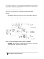
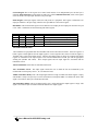
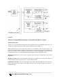
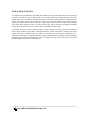
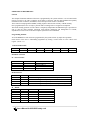
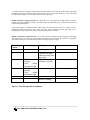
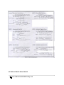
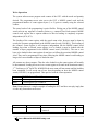
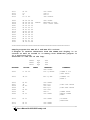
8251 AND 8253
PROGRAMMABLE COMMUNICATION INTERFACE AND
PROGRAMMABLE INTERVAL TIMER
1. INTRODUCTION
Electro System Associates Private Limited (ESA) manufactures trainers for most of the popular
microprocessors like 8085, Z-80, 8031,8086/88,68000 and 80196. ESA offers a variety of modules, which
can be interfaced, to these trainers. These modules can be effectively used for teaching/training in the
laboratories.
The 8251 and 8253 study card incorporates Intel’s 8251 and 8253. The interface is designed to explain all the
facilities available in 8251 and 8253.
Functional description of 8251 and 8253, implementation of the circuit and some simple software are
presented in this manual.
2. DESCRIPTION OF THE CIRCUIT:
The study card provides 8251 as well as timer section. The interface has got 4 connectors.
J3,J4 and P1 used for various trainer kits. J2 (10 pin FRC right angle male connector) is used for connecting
RS232C cable to the COM port of the system. 10 RED LEDs are provided to indicate the important signals.
6.144MHz crystal is provided to drive 1.5 MHz clock.
The following table describes the various hardware configurations for 8251 and 8253 using jumper
settings.
Jumper
JP1
JP2
JP3
JP4
JP5
JP6
JP7
JP8
Position
1-2
*2-3
1-2
*2-3
1-2
*2-3
1-2
*2-3
OPEN
*CLOSED
*OPEN
CLOSED
*OPEN
CLOSED
*OPEN
CLOSED
Description
GATE1 is connected externally.
GATE1 is connected to VCC.
GATE2 is connected externally.
GATE2 is connected to VCC.
CLK1 is derived externally.
1.5 Mhz clock is given to CLK1.
OUT1 is given to CLK2.
CLK2 is derived externally.
CLK0 is left unconnected.
1.5Mhz clock is given to CLK0.
RxD and TxD are not shorted.
RxD and TxD are shorted.
CTS and RTS are not shorted.
CTS and RTS are shorted.
8251 chip select derived from decoder.
8251 chip select derived externally.
User’s Manual for 8251/8253 study card
1
3.0 INSTALLATION:
Please refer the below table for connection procedure for various trainer
kits.
Sl. No
Model No.
1
MPS 85-3
Studycard
Adapter
No Adapter
Connection Procedure
2
ESA 85-2
No Adapter
3
ESA 86/882
Study card adapter
for
ESA 86-2/3
trainer
4
ESA 86/883
Study card adapter
for
ESA 86-2/3
trainer
Connect 50 pin FRC cables between J1, J2 of the adapter
with J1,J2 of the trainer kit.
Connect 26 pin FRC cables between J3,J4 of the adapter with
J3,J4 of the study card respectively.
5
ESA 86E
No Adapter
6
ESA 31
Study Card adapter
ESA 31/51 Trainer
7
ESA 51
Study Card adapter
ESA 31/51 Trainer
8
ESA 51E
ESA 51E Study
card adapter.
Connect 26 pin FRC cables between J3, J4 of study card with
J6 ,J7 of the trainer kit respectively.
Connect 50 pin FRC cable between J1 of adapter with J5 of
the trainer kit.
Connect 26 pin FRC cables between J3,J4 of adapter with
J3,J4 of the study card respectively.
Connect 50 pin FRC cable between J1 of adapter with J1 of
the trainer kit.
Connect 26 pin FRC cables between J3,J4 of adapter with
J3,J4 of the study card respectively.
Connect 50 pin FRC cable between P3 of adapter with P1 of
study card.
Connect 26 pin FRC cables between J3 ,J4 of adapter with
J4,J6 of the trainer kit respectively.
Connect 26 pin FRC cables between J3, J4 of study card with
J3 ,J4 of the trainer kit respectively.
Connect 50 pin FRC cable between P1 of study card with P1
of the trainer kit .
Connect 50 pin FRC cables between J1, J2 of the adapter
with J1,J2 of the trainer kit.
Connect 26 pin FRC cables between J3,J4 of the adapter with
J3,J4 of the study card respectively.
The 8251A programmable communication interface
The 8251A is a programmable chip designed for synchronous and a synchronous serial data communication,
packaged in a 28 – pin DIP. The 8251A is the enhanced version of its predecessor, the 8251, and it is
compatible with the 8251. Figure1 shows the block diagram of the 8251A. It includes 5 sections: Read/Write
Control Logic, Transmitter, Receiver, Data Bus Buffer, and Modem Control.
The control logic interfaces the chip with the MPU, determines the function of the chip according to the
control word in its register (to be explained below), and monitors the data flow. The transmitter section
converts a parallel word received from the MPU into serial bits and transmits them over the TxD line to a
peripheral. The receiver section receives serial bits from a peripheral, converts them into a parallel word, and
transfers it to MPU. The 8251A is a complex device capable of performing various functions. For the sake of
clarity, this chapter focuses only on the asynchronous mode of serial I/O, and excludes any discussion of the
synchronous mode and the modem control. The asynchronous mode is often used for the data communication
between the MPU and serial peripherals such as terminals and floppy disks.
User’s Manual for 8251/8253 study card
2
Figure 2 shows an expanded version of the 8251A block diagram. The block diagram shows all the elements
of a programmable chip; It includes the interfacing signals, the control register, and the status register. The
functions of the various blocks are described below.
READ/WRITE CONTROL LOGIC AND REGISTERS
This section includes R/W control logic, six input signals, control logic and three buffer registers: data
register, control register, and status register. The input signals to the control logic are as follows.
Input signals
CS*-chip select: When this signal goes low, the 8251A is selected by the MPU for communication.
This is usually connected to a decoded address bus.
C/D*-control/data: when this signal is high, the control register or the status register is addressed.
The control register and the status register are differentiated by WR* and RD* signals, respectively.
FIGURE 2: The 8251A: Expanded Block Diagram of Control Logic and Registers
WR*-Write: When this signal goes low, the MPU either writes in the control register or sends
output to the data buffer. This is connected to IOW* or MEMW*.
RD*-Read: When this signal goes low, the MPU either reads a status register or accepts (input) data
from the data buffer. This is connected to either IOR* or MEMR*
RESET-Reset: A high on this input resets the 8251A and forces it into the idle mode.
CLK-Clock: This is the clock input, usually connected to the system clock. This clock does not
control either the transmission or the reception rate. The clock is necessary for communication with
the microprocessor.
User’s Manual for 8251/8253 study card
3
Control Register This 16-bit register for a control word consists of two independent bytes: the first byte is
called the mode instruction (word) and the second byte is called command instruction (word). This register
can be accessed as an output port when the C/D* pin is high.
Status Register: This input register checks the ready status of a peripheral. This register is addressed as an
input port when the C/D* pin is high, it has the same port address as the control register.
Data Buffer :This bi-directional register can be addressed as an input port and output port when the C/D* pin
is low. Table 1 summarizes all the interfacing and control signals.
CS*
0
0
0
0
1
C/D*
1
1
0
0
X
RD*
1
0
1
0
X
WR*
0
1
0
0
X
Function
MPU writes instructions in the control register.
MPU reads status from the status register
MPU outputs data to the Data Buffer
MPU accepts data from the Data Buffer
USART is not selected.
TRANSMITTER SECTION
The transmitter accepts parallel data from the MPU and converts them into serial data . It has two registers: a
buffer register to hold eight bits and an output register to convert eight bits into steam of serial bits (figure 3)
.the MPU writes a byte in the buffer register . whenever the output register is empty, the contents of the buffer
register are transferred to the output register. This section transmits data on TxD pin with the appropriate
framing bits (START and STOP) . Three output signals and one input signal are associated with the
transmitter section.
TxD-Transmit Data: Serial bits are transmitted on this line.
TxC*-Transmitter Clock: This input signal controls the rate at which the bits are transmitted by the
USART.The clock frequency can be 1,16 or 64 times the baud.
TxRDY-transmitter Ready: This is the output signal. When it is high, it indicates the buffer register is empty
and USART is ready to accept a byte .It can be used either to interrupt the MPU or to indicate the status. This
signal is reset when a data byte is loaded into the buffer.
TxE-Transmitter Empty: This is an output signal. Logic 1 on this indicates the output register is empty. This
signal is reset when a byte is transferred from the buffer to the output register.
User’s Manual for 8251/8253 study card
4
FIGURE 3
The 8251A: Expanded Block Diagram of Transmitter and Receiver Section
RECEIVER SECTION
The receiver accept serial data on the RxD line from a peripheral and converts them into parallel data . The
section has two registers: the receiver input register and the buffer register (figure 3).
When the RxD line goes low, the control logic assumes it is a START bit , waits for half a bit time , and
sample the line again. If the line is still low , the input register accepts the following bits, form a character ,and
load it into the buffer register. Subsequently, the parallel byte is transferred to the MPU when requested. In
the asynchronous mode , two input signal and one output signal are necessary ,as described below.
RxD-Receive Data: Bits are received serially on this line and converted into a parallel byte in the receiver
input register.
RxC-Receiver clock: This is a clock signal that controls the rate at which bits are received by the USART. In
the asynchronous mode, the clock can be set to 1,16 or 64 times the baud.
RxRDY-Receiver Ready: This is an output signal. It goes high when the USART has a character in the
buffer register and is ready to transfer into the MPU. This line can be used either to indicate the status or to
interrupt the MPU
User’s Manual for 8251/8253 study card
5
INITIALIZING THE 8251A
To implement serial communication, the MPU must inform the 8251A of all details such as mode, baud, stop
bits, parity, etc. Therefore, prior to data transfer, a set of control words must be loaded into the 8 -bit control
register of the 8251A. In addition, the MPU must check the readiness of the peripheral by reading the status
register. The control words are divided into two formats: mode words and command words. The mode word
specifies the general characteristics of operation ( such as baud , parity, number of stop bits),the command
word enable data transmission and /or reception, and the status word provides the information concerning
register status and transmission errors. Figure 4 shows the definition of these words.
To initialize the 8251A in the asynchronous mode, a certain sequence of control words must be followed.
After a Reset operation (system Reset or through instruction), a mode word must be written in the control
register followed by a command word. Any control word written in the control register immediately after a
word will be interpreted as a command word ,that means a command word can be changed any time during the
operation. However, the 8251A should be reset prior to writing a new mode word, and it can be reset by using
the Internal Reset bit (D6) in the command word.
User’s Manual for 8251/8253 study card
6
Note: * indicates active low signal
FIGURE 4
Mode Word Format (A),Command Word Format (B) and Status word Format (C)
User’s Manual for 8251/8253 study card
7
User’s Manual for 8251/8253 study card
8
User’s Manual for 8251/8253 study card
9
FIGURE 1
The 8251 A: Block Diagram, Pin Configuration and Description.
User’s Manual for 8251/8253 study card
10
8253 / 8253-5
PROGRAMMABLE INTERVAL TIMER
MCS-85TM Compatible 8253-5
3 Independent 16-Bit Counter
DC to 2 MHz
Programmable Counter Modes
Count Binary or BCD
Single +5V Supply
24-Pin dual In –line Package
The Intel R 8253 is a programmable counter/timer chip designed for use as an Intel microcomputer peripheral.
It uses nMOS technology with a single +5V supply and is packaged in a 24 pin plastic DIP.
It is organized as 3 independent 16 bit counters, each with a count rate of up to 2 Mhz. All modes of operation
are software programmable.
User’s Manual for 8251/8253 study card
11
FUNCTIONAL DESCRIPTION
General
The 8253 is a programmable interval timer/counter specifically designed for use with the Intel TM
microcomputer systems. Its function is that of a general purpose ,multi-timing element that can be treated as
an array of I/O ports in the system software.
The 8253 solves one of the most common problems in the microcomputer system , the generation of accurate
time delays under software control. Instead of setting up timing loops in system software ,the programmer
configures the 8253 to match his requirements, initialize one of the counter of 8253 with the desired quantity
, then upon command the 8253 will count out the delay and interrupt the CPU when it has completed its tasks
it is easy to easy to see that the software overhead is minimal and that multiple delays can easily be maintained
by assignment of priority levels.
Other counter / timer functions that are non delay in nature but also common to most microcomputers can be
implemented with the 8253.
Programmable Rate Generator
Event Counter
Binary rate multiplier
Real Time Clock
Digital One -shot
Complex Motor controller
Data Bus Buffer
This 3-state, bi-directional, 8-bit buffer is used to interface the 8253 to the system data bus. Data is
transmitted or received by the buffer upon execution of IN put or OUT put CPU instructions. The Data Bus
Buffer has three basic functions
1.
2.
3.
Programming the MODES of the 8253.
Loading the count registers.
Reading the count values.
Read/Write Logic
The Read/Write Logic accepts inputs from the system bus and in turn generates control
signals for overall device operation. It is enabled or disabled by CS so that no operation can
occur to change the function unless the device has been selected by the system logic.
RD*(Read)
A “low” on this input informs the 8253 that the CPU is inputting the data in the form of a counter value.
WR*(Write)
A “low” on this input informs the 8253 that the CPU is outputting the data in the form of mode information or
loading counters
User’s Manual for 8251/8253 study card
12
A0, A1
These inputs are normally connected to the address bus. Their function is to select one of the three counters to
be operated on and to address the control word register for mode selection.
CS*(Chip Select)
A “low” on this input informs the 8253. No reading or writing will occur unless the device is selected. The
CS*input has no effect upon the actual operation of the counters.
CS*
0
0
0
0
0
0
0
0
1
0
RD*
1
1
1
1
0
0
0
0
X
1
WR*
0
0
0
0
1
1
1
1
X
1
A1
0
0
1
1
0
0
1
1
X
X
A0
0
1
0
1
0
1
0
1
X
X
Load Counter No.0
Load Counter No.1
Load Counter No.2
Write Mode Word
Read Counter No.0
Read Counter No.1
Read Counter No.2
No-operation 3 state
Disable 3 state
No-operation 3 state
User’s Manual for 8251/8253 study card
13
Control Word Register
The control word register is selected when A0, A1 are 11. It then accepts information from the data bus buffer
and stores it in a register. The information stored in this register controls the operational MODE of each
counter, selection of binary or BCD counting and the loading of each count register.
The Control Word Register can only be written into; no read operation of its contents is available.
Counter #0, counter#1, counter#2
These three function blacks are identical in operation so only a single counter will be described. Each
Counter consists of a single ,16, pre-settable , DOWN counter. The counter can operate in either binary or
BCD and its input, gate and output are configured by the selection of MODES stored in the Control Word
Register.
The counters are fully independent and each can have separate Mode configuration and counting operation,
binary or BCD. Also ,there are special features in the control word that handle the loading of the count value
so that software overhead can be minimized for these functions .
The reading of the contents of each counter is available to the programmer with simple READ operations for
event counting applications and special commands and logic are included in the 8253 so that the contents of
each counter can read “on the fly” without having to inhibit the clock input.
8253 SYSTEM INTERFACE
The 8253 is a component of the Intel TM microcomputer systems and interfaces in the same manner as all
other peripherals of the family. It is treated by the system software as an array of peripheral I/O ports ; three
are counters and the fourth is a control register for MODE programming.
Basically, the select inputs A0, A1 connect to the A0,A1 address bus signals of the CPU. The CS* can be
derived directly from the address bus using a linear select method. Or it can be connected to the output of a
decoder, such as an Intel 8205 for larger systems.
Figure 4: Block Diagram Showing Control Word Register and Counter Functions.
User’s Manual for 8251/8253 study card
14
OPERATIONAL DESCRIPTION
General
The complete functional definition of the 8253 is programmed by the systems software. A set of control words
must be sent out by the CPU to initialize each counter of the 8253 with the desired MODE and quantity
information. Prior to initialize, the MODE, count, and output of all counters is undefined.
These control words program the MODE, Loading sequence and selection of binary or BCD counting.
Once programmed, the 8253 is ready to perform whatever timing tasks it is assigned to accomplish.
The actual counting operation of each counter is completely independent and additional logic is provided onchip so that the usual problems associated with efficient monitoring and management of external,
asynchronous events or rates to the microcomputer system have been eliminated.
Programming the 8253
All of the MODES for each counter are programmed by the system software by simple I/O operations.
Each counter of the 8253 is individually programmed by writing a control word in to the control word
register. (A0 A1=11).
Control Word Format
D7
SC1
D6
SC0
D5
RL1
D4
RL0
D3
M2
D2
M1
D1
M0
D0
BCD
Definition of Control
SC –Select Counter:
SC1
0
0
1
1
SC0
0
1
0
1
Select Counter 0
Select Counter 1
Select Counter 2
Illegal
RL-Read/Load:
RL1
0
1
0
1
RL0
0
0
1
1
Counter latching operation (see READ/WRITE procedure section)
Read/Load most significant byte only.
Read/Load least significant byte only.
Read/Load least significant byte first, then most significant byte.
M1
0
0
1
1
0
0
M0
0
1
0
1
0
1
M _ MODE
M2
0
0
X
X
1
1
Mode 0
Mode 1
Mode 2
Mode 3
Mode 4
Mode 5
User’s Manual for 8251/8253 study card
15
BCD:
0
1
Binary Counter 16 bits
Binary Coded Decimal (BCD) Counter ( 4 Decades)
Counter Loading
The count register is not loaded until the count value is written (one or two bytes, depending on the mode
selected by the RL bits), followed by a rising edge and a falling edge of the clock. Any read of the counter
prior to that falling clock edge may yield invalid data.
Mode Definition
MODE 0: Interrupt on Terminal count. The output will be initially low after the mode set operation. After
the count is loaded into the selected count register, the output will remain low and the counter will count.
When the terminal count is reached the output will go high and remain high until the selected count register is
reloaded with the mode or a new count is loaded. The counter continues to decrement after terminal count has
been reached.
Rewriting a counter register during counting result in the following
1.
2.
Write 1st byte stops the current counting.
Write 2nd byte start the new count.
MODE 1: Programmable One-Shot. The output will go low on the count following the rising edge of the
gate input.
The output will go high on the terminal count. If a new count value is loaded while the output is low it will not
affect the duration of the one –shot pulse until the succeeding trigger. The current count can be read at any
time without affecting the one-shot pulse.
The one–shot is retriggerable, hence the output will remain low for the full count after any rising edge of the
gate input.
MODE 2: Rate Generator. Divide by N counter. The output will be low for one period of the input clock.
The period from the output pulse to the next equals the number of input counts in the count register. If the
count register is reloaded between output pulses the present period will not be affected, but the subsequent
period will reflect the new value.
The gate input, when low, will force the output high. When the gate input goes high, the counter will start
from the initial count. Thus the gate input can be used to synchronize the counter
When this mode is set, the output will remain high until after the counter register is loaded. The output then
can also synchronized by software.
Mode 3: Square Wave Rate Generator. Similar to MODE 2 except that the output will remain high until
one half the count has been completed (for even numbers) and go low for the other half of the count. This is
accomplished by decrementing the counter by two on the falling edge of each clock pulse. When the counter
reaches terminal count , the state of the output is changed and the counter is reloaded with the full count and
the whole process is repeated .
If the count is odd and the output is high, the first clock pulse (after the count is loaded) decrements the count
by 1. Subsequent clock pulses decrement the clock by 2. After timeout, the output goes low and the full count
User’s Manual for 8251/8253 study card
16
is reloaded. The first clock pulse (following the reload) decrements the counter by 3. Subsequent clock pulses
decrement the count by 2 until the timeout. Then the whole process is repeated in this way, if the count is odd,
the output will be high for (N+1)/2 counts and low for (N-1)/2 counts.
MODE 4:Software Triggered Strobe. After the mode is set , the output will be high. When the count is
loaded. The counter will begin counting . On terminal count, the output will go low for one input clock period,
and then will go high again.
If the count register is reloaded between output pulses, the present period will not be affected, but the
subsequent period will reflect the new value. The count will be inhibited while the gate input is low.
Reloading the counter register will restart counting beginning with new number.
MODE 5: Hardware Triggered strobe. The counter will start counting after the rising edge of the trigger
input and will go low for one clock period when the terminal count is reached. The counter is retriggerable.
The output will not go low until the full count after the rising edge of any trigger
Modes/Signa
l Status
0
1
2
3
4
5
Low Or going low Rising
High
Disables counting
Enables counting
1.Initiates counting
2.Resets output after
next clock
1.Reloads counter
Enables counting
2.Initiates counting
1.Disables
counting
2.Sets
output
immediately high
1.Disables
Initiates counting
counting
2.Sets
output
immediately high
Disables counting
Initiates counting
Enables counting
Enables counting
Figure 6. Gate Pin Operations Summary.
User’s Manual for 8251/8253 study card
17
8253 READ/WRITE PROCEDURE
User’s Manual for 8251/8253 study card
18
Write Operations
The system software must program each counter of the 8253 with the mode and quantity
desired. The programmer must write out to the 8253 a MODE control word and the
programmed number of count register bytes (1 or 2) prior to actually using the selected
counter.
The actual order of the programming is quite flexible. Writing out of the MODE control
word can be in any sequence of counter section, e.g., counter#2 last. Each counter’s MODE
control word register has a separate address so that its loading is completely sequence
independent. (SC0, SC1).
The loading of the count register with the actual count value, however must be done in
exactly the sequence programmed in the MODE control word ( RL0,RL1). This loading of
the counter’s count register is still sequence independent like the MODE control word
loading, but when a selected count register is to be loaded it must be loaded with the
number of bytes programmed in the MODE control word ( RL0-RL1). The one or two
bytes to be loaded in the count register do not have to follow the associated MODE control
word. They can be programmed at any time following the MODE control word loading as
long as the correct number of bytes is loaded in order.
All counters are down counters. Thus the value loaded in to the count register will actually
be decremented. Loading all zeroes in to a count register will result in the maximum count (
2 16 for binary or 104 for BCD). In MODE 0 the new count will not restart until the load has
been completed. It will accept one of two bytes depending on how the MODE control
words ( RL0-RL1) are programmed. Then proceed with the restart operation.
LSB
MSB
MODE Control Word Counter n
Count Register byte Counter n
Count Register byte Counter n
Note: Format shown is a simple example of loading the 8253 and does not reply imply that
it is the only format that can be used.
No.1
MODE control Word
Counter 0
User’s Manual for 8251/8253 study card
A1
1
A0
1
19
No.2
No.3
No.4
LSB
No.5
MSB
No.6
LSB
No.7
MSB
No.8
LSB
No.9
MSB
MODE control Word
Counter 1
MODE control Word
Counter 2
Count Register Byte Counter
1
Count Register Byte Counter
1
Count Register Byte Counter
2
Count Register Byte Counter
2
Count Register Byte Counter
0
Count Register Byte Counter
0
1
1
1
1
0
1
0
1
1
0
1
0
0
0
0
0
Note: The exclusive addresses of each counter’s count register make the task of programming the 8253 a very
simple matter, and maximum effective use of the device will result if this feature is fully utilized.
Figure 9. Alternating Programming Formats.
Read operations
In most counter applications it becomes necessary to read the value of the count in progress
and make a computational decision based on this quantity. Event counters are probably the
most common application that uses this function. The 8253 contains logic that will allow
the programmer to easily read the contents of any of three counters without disturbing the
actual count in progress.
There are two methods that the programmer can use to read the value of the counters. The
first method involves the use of simple I/O read operations of the selected counter. By
controlling the A0, A1 inputs to the 8253 the programmer can select the counter to be read (
remember that no read operation of the mode register is allowed. A0, A1-A11). The only
requirement with this method is that in order to assure a stable count reading the actual
operation of the selected counter must be inhibited either by controlling the Gate input or
by external logic that inhibits the clock input. The contents of the counter selected will be
available as follows.
First I/O Read contains the least significant byte (LSB).. Second I/O Read contains the most
significant byte (MSB).
User’s Manual for 8251/8253 study card
20
Due to the internal logic of the 8253 it is absolutely necessary to complete the entire
reading procedure. If two bytes are programmed to be read then two bytes must be read
before any loading WR commands can be sent to the same counter.
Read Operation Chart
A1
A0
0
0
0
1
1
0
1
1
RD
0
0
0
0
Read Counter No.0
Read Counter No.1
Read Counter No.2
Illegal
Reading While Counting
The order for the programmer to read the contents of any counter without effecting or
disturbing the counting operation the 8253 has special internal logic that can be accessed
using simple WR commands to the MODE register. Basically in the programmer wishes to
read the contents of a selected counter “ on the fly” he loads the MODE register with a
special code which lathes
MODE Register for Latching count
A0,A1=11
D7
SC1
D6
SC0
D5
0
D4
0
D3
X
D2
X
D1
X
D0
X
SC1,SC0-Specify counter to be latched.
D5,D4-D0 designates counter latching operation.
X-don’t care
The same limitation applies to this mode of reading the counter as the previous method.
That is, it is mandatory to complete the entire read operation as programmed. This
command has no effect on the counter’s mode.
User’s Manual for 8251/8253 study card
21
4.0 Demonstration programs for 8085 Series kits.
Sample programs for MPS 85-3 and ESA 85-2 trainer
1. Program to display "WELCOME TO ESA 8251 STUDY CARD" for 9600
baud by initializing 8251.Execute the program from 8000H.
CMD53
CMD51
DAT51
ADDRESS
OPCODE
EQU
EQU
EQU
LABLE
83H
91H
90H
MNOMONIC
COMMENTS
ORG 8000H
8000
11 0A 00
LXI D,000AH
8003
3E 36
MVI A,36H
8005
8007
8008
800A
800B
800D
800E
D3
7B
D3
7A
D3
AF
D3
83
91
OUT
MOV
OUT
MOV
OUT
XRA
OUT
CMD53
A,E
80H
A,D
80H
A
CMD51
8010
8012
8014
8016
8118
801A
801C
D3
D3
D3
3E
D3
3E
D3
91
91
91
40
91
CE
91
OUT
OUT
OUT
MVI
OUT
MVI
OUT
CMD51
CMD51
CMD51
A,40H
CMD51
A,0CEH
CMD51
801E
3E 27
MVI A,27H
8020
8022
D3 91
21 00 90
OUT CMD51
LXI H,9000H
8025
06 33
MVI B,33H
8027
DB 91
8029
802B
802D
E6 81
FE 81
C2 27 80
ANI 81H
CPI 81K
JNZ STATUS
8030
7E
MOV A,M
80
80
STATUS:
IN CMD51
User’s Manual for 8251/8253 study card
;TIMER 0 for
;9600 BAUD
;TIMER 0 IN
;MODE 3
;LOAD LSB VALUE
;LOAD MSB VALUE
;DUMMY MODE
;WRITE DUMMY
;word
;IN MODE reg
;RESET 8251
;SET 8251 FOR
;ASYNCHRONOUS 16
;16X baud.
;2 STOP BITS,8
;data bits,
;No parity
;WRITE COMMAND
;Word
;MEMORY TO STORE
;the character
;CHARACTER
;GET USART
;status
;RECEIVER READY
;NO,WAIT
;GET CHARACTER
;FROM USART
22
8031
8033
8034
8035
D3 90
23
05
C2 27 80
9000
9004
9008
900C
9010
9014
9018
901C
9020
9024
9028
902C
9030
0A
0A
20
20
20
45
4D
4F
41
35
54
20
44
0A
0A
20
20
20
4C
45
20
20
31
55
43
2E
0A
0A
20
20
20
43
20
45
38
20
54
41
0D
OUT
INX
DCR
JNZ
0A
20
20
20
57
4F
54
53
32
53
59
52
OA
TABLE:
DAT51
H
B
STATUS
ORG 9000H
WELCOME TO ESA
8251 STUDY CARD
**********************************************************************************
Sample programs for MPS 85-3 and ESA 85-2 trainer
2.Program to receive characters from the USART and display it on
console as well as stored it in memory from 8500H.The program is
in a continuous loop
Press ESC to come out of the loop.
CMD53
CMD51
DAT51
ADDRESS
OPCODE
EQU
EQU
EQU
8000
11 0A 00
MNEMONIC
ORG 8000H
LXI D,000AH
8003
3E 36
MVI A,36H
8005
8007
8008
800A
800B
800D
800E
D3
7B
D3
7A
D3
AF
D3
OUT
MOV
OUT
MOV
OUT
XRA
OUT
8010
D3 91
OUT CMD51
8012
8014
D3 91
D3 91
OUT CMD51
OUT CMD51
83
80
80
91
LABLE
83H
91H
90H
User’s Manual for 8251/8253 study card
CMD53
A,E
80H
A,D
80H
A
CMD51
COMMENTS
;TIMER 0 for
;9600 BAUD
;TIMER0 IN
;MODE 3
;LOAD LSB VALUE
;LOAD MSB VALUE
;DUMMY MODE
;WRITE DUMMY
;WORD
;IN MODE
;REGISTER
23
8016
8018
801A
801C
3E
D3
3E
D3
40
91
CE
91
MVI
OUT
MVI
OUT
801E
3E 27
MVI A,27H
8020
8022
D3 91
21 00 85
OUT CMD51
LXI H,8500H
8025
CD 37 80
8028
8029
802B
802E
8031
8032
8C33
8036
8037
79
FE
CA
CD
71
23
C3
EF
DB
8039
803B
803E
8040
8041
8042
8044
8046
8048
804B
804C
804E
E6
CA
DB
4F
C9
DB
E6
FE
C2
79
D3
C9
BACK:
CALL GETCH
DOWN:
GETCH:
MOV A,C
CPI 27
JZ DOWN
CALL SOUTPT
MOV M,C
INX H
JMP BACK
RST 5
IN CMD51
1B
36 80
42 60
25 80
91
02
37 80
90
91
81
81
42 80
A,40H
CMD51
A,0CEH
CMD51
SOUTPT:
90
ANI 02H
JZ GETCH
IN DAT51
MOV C,A
RET
IN CMD51
ANI 81H
CPI 81H
JNZ SOUTPT
MOV A,C
OUT DAT51
RET
;RESET 8251
;SET 8251 FOR
;ASYNCHRONOUS
;16XBAUD,
;2 STOP BITS,8
;DATA
;BITS,NO PARITY
;WRITE COMMAND
;WORD
;MEMORY TO STORE
;THE
;CHARACTER TO
;MEMORY
;GET USART
;STATUS
;RECEIVER READY
;NO,WAIT
;GET CHARACTER
;FROM USART
****************************************************************
Sample programs for MPS 85-3 and ESA 85-2 trainer
3. Initialize Timer 1 and display the count on Data field of the
trainer display. Execute the program from 8000H.The program is in
a continuous loop, press RESET key to come out of the loop.
CMD53
CMD51
EQU
EQU
83H
91H
User’s Manual for 8251/8253 study card
24
DAT51
EQU
LABLE
90H
ADDRESS
OPCODE
8000
21 FF FF
MNEMONIC
ORG 8000H
LX1 H,0FFFFH
8003
8005
8007
8008
800A
800B
800D
800F
8011
8013
8015
3E
D3
7D
D3
7C
D3
3E
D3
3E
D3
3E
76
83
MVI
OUT
MOV
OUT
MOV
OUT
MVI
OUT
MVI
OUT
MVI
8017
8019
801B
801E
8020
8023
8025
8028
802B
802E
8030
8032
8033
8034
8035
8036
8037
803A
803B
803E
803F
8041
D3
DB
32
FE
CA
06
CD
CD
C3
16
1E
1D
00
00
00
00
C2
15
C2
C9
3E
C3
83
82
Fl
80
3F
00
4C
2E
15
FF
33
81
81
96
83
FF
82
86
ODT:
8F
80
04
80
80
DLY:
LP1:
LP:
32 80
30 80
70
13 80
NDT:
A,76H
CMD53
A,L
81H
A,H
81H
A,96H
CMD53
A,0FFH
82H
A,86H
COMMENTS
;INITIALISE
;TIMER 1
;FOR MODE 3
;LSB OF TIMER 1
;MSB OF TIMER 2
;LODE MODE WORD
;LATCH COMMAND
;WORD
OUT CMD53
IN 82H
STA 8FF1H
CPI 80H
JZ NDT
MVI B,00H
CALL 044C
CALL DLY
JMP ODT+2
MVI D,0FFH
MVI E,33H
DCR E
NOP
NOP
NOP
NOP
JNZ LP
DCR D
JNZ LP1
RET
MVI A,70H
JMP ODT
Sample programs for MPS 85-3 and ESA 85-2 trainer
4. Program to display "DEMO PROGRAM FOR AYSNCHRONOUS COMMUNICATION
IN INTERRUPT MODE" by using interrupt driven. Execute the program
from 8000H.
ADDRESS
OPCODE
LABLE
8000
11 0A 00
MNOMONIC
ORG 8000H
LXI D,000AH
8003
3E 36
MVI A,36H
User’s Manual for 8251/8253 study card
COMMENTS
;TIMER 0 for
;9600 baud
;TIMER 0 IN
25
;MODE 3.
8005
8007
8008
800A
800B
800D
800E
8010
8012
8014
8016
8018
801A
801C
D3
7B
D3
7A
D3
AF
D3
D3
D3
D3
3E
D3
3E
D3
83
OUT
MOV
OUT
MOV
OUT
XRA
OUT
OUT
OUT
OUT
MVI
OUT
MVI
OUT
801E
3E 27
MVI A,27H
8020
8022
D3 91
21 00 90
OUT CMD51
LXI H,9000H
8025
8027
8029
802A
802B
802C
802E
8031
8032
8033
8034
8036
8037
8038
8039
803A
06
3E
30
FB
78
F6
C2
EF
F5
7E
D3
23
05
F1
FB
C9
45
0E
9000
9005
900A
900F
9014
9019
901E
9023
9028
902D
9032
9037
0A
44
50
41
52
4E
4E
43
4E
49
4E
45
0A
45
52
4D
20
43
4F
4F
49
4F
20
52
80
80
91
91
91
91
40
91
CE
91
00
2B 80
90
20
4D
4F
20
41
48
55
4D
43
4E
49
52
CMD53
A,E
80H
A,D
80H
A
CMD51
CMD51
CMD51
CMD51
A,40H
CMD51
A,0CEH
CMD51
MVI B,45H
MVI A,0EH
SIM
EI
LOOP: MOV A,B
ORI 0
JNZ LOOP
RST 5
STATUS:
PUSH PSW
MOV A,M
OUT DAT51
INX H
DCR B
POP PSW
EI
RET
20
4F
47
46
53
52
53
4D
41
20
4E
55
20
20
52
4F
59
4F
20
55
54
49
54
50
;LOAD LSB VALUE
;LOAD MSB VALUE
;DUMMY MODE
;WRITE DUMMY WORD
;IN MODE REGISTER
;RESET 8251
;SET 8251 FOR
;ASYNCHRONOUS
;16XBAUD,
;2 STOP BITS,8
;DATA BITS
;NO PARITY
;WRITE COMMAND
;WORD
;MEMORY TO STORE
;THE
;CHARACTER
;ENABLE RST 5.5
TABLE:ORG 9000H
DEMO PROGRAM FOR
ASYNCHRONOUS
COMMUNICATION IN
INTERUPT MODE
User’s Manual for 8251/8253 study card
26
903C
9041
54 20 4D 4F 44
45 2E 0D 0A 00
ORG 8FB3H
8FB3
C3 32 80
JMP STATUS
****************************************************************
5.0 Demonstration programs for 8051 Series kits.
EXAMPLE PROGRAMS FOR ESA 31/51 TRAINERS
1.Program to display "WELCOME TO ESA 8251 STUDY CARD" for 9600
baud by initializing 8251. Execute the Program at 8000H.
CONTROL REGISTER = F183
DATA PORT
= F190
COMMAND PORT
= F191
ADDRESS
OPCODE
LABLE
8000
74 36
MNEMONIC
ORG 8000H
MOV A,#36H
8002
8005
8006
8009
800B
800C
800E
800F
8012
8013
8014
8015
8016
8018
8019
90
F0
90
74
F0
74
F0
90
F0
F0
F0
F0
74
F0
74
MOV DPTR,#0F183H
MOVX @DPTR,A
MOV DPTR,#0F180H
MOV A,0AH
MOVX @DPTR,A
MOV A,#00H
MOVX @DPTR,A
MOV DPTR,#0F191H
MOVX @DPTR,A
MOVX @DPTR,A
MOVX @DPTR,A
MOVX @DPTR,A
MOV A,#40H
MOVX @DPTR,A
MOV A,#0CEH
801B
801C
801E
801F
8022
8024
F0
74
F0
90
79
C0
8026
8028
802B
802C
802E
8030
8032
8035
8037
8038
803B
C0
90
E0
54
D0
D0
B4
74
93
B4
02
F1 83
F1 80
0A
00
F1 91
40
CE
01
90 00
00
83
82
F1 91
81
82
83
01 EF
00
00 03
00 00
STATUS:
COMMENTS
;Timer0 for
;9600 baud
;in mode3
;USART
;Reset 8251
MOVX @DPTR,A
MOV A,#01H
MOVX @DPTR,A
MOV DPTR,#9000H
MOV R1,#00H
PUSH DPH
;Get USART
;Status
PUSH DPL
MOV DPTR,#0F191H
MOVX A,@DPTR
ANL A,#81H
POP DPL
POP DPH
CJNE A,#01H,STATUS
MOV A,#00H
MOVC A,@A+DPTR
CJNE A,#00H,CONT
LJMP 0
User’s Manual for 8251/8253 study card
27
803E
8040
8042
8045
8046
8048
804A
804B
C0
C0
90
F0
D0
D0
A3
80
83
82
F1 90
9000
9005
9008
900D
9010
0A
0A
20
20
57
0A
0A
20
20
45
9015
9D1A
901F
9024
9029
4D 45 20
20 45 53
53 54 55
20 43 41
0D 00
CONT:
82
83
D7
0A 0A 0A
0A
20 20 20
20
4C 43 4F
54
41
44
52
PUSH DPH
PUSH DPL
MOV DPTR,#0F190H
MOVX @DPTR,A
POP DPL
POP DPH
INC DPTR
SJMP STATUS
ORG 9000H
TABLE: DB 0AH,0AH,0AH,0AH,0AH
DB 0AH,0AH,0AH
DB 20H,20H,20H,20H,20H
DB 20H,20H,20H
DB ‘WELCOME TO ESA STUDY
CARD’,0DH,00H’
4F
20
59
44
EXAMPLE PROGRAMS FOR ESA 31/51 TRAINERS
2.Program to receive characters from the USART and display it on
Console as well as stored it in memory from 9000h. The program is
in a continuous loop, press ESC to come out from the loop. Execute
the Program at 8000H.
ADDRESS
OPCODE
8000
8002
8005
B006
8009
800B
800C
800E
800F
74
90
F0
90
74
F0
74
F0
90
8012
8013
F0
F0
36
Fl 83
Fl 80
0A
00
Fl 91
LABLE
MNEMONIC
COMMENTS
ORG 8000H
MOV A,#36H
MOV DPTR,#0F183H ;TIMER 0 CMD
MOVX @DPTR,A
MOV DPTR,#0F180H
MOV A,#0AH
;TIMER 0DATA
MOVX @DPTR,A
MOV A,#00H
MOVX @DPTR,A
MOV DPTR,#0F191H
;Initialize
;USART
MOVX @DPTR,A
MOVX @DPTR,A
User’s Manual for 8251/8253 study card
28
8014
8015
8016
8018
8019
801B
801C
801E
801F
F0
F0
74
F0
74
F0
74
F0
90
8022
8024
8026
8029
802A
802C
802E
8031
8032
8034
8037
803A
803D
C0
C0
90
E0
54
60
90
E0
F5
B4
02
90
E0
803E
54 01
8040
B4 01 FA
8043
8045
8048
8049
804B
804D
804E
8050
E5 F0
90 Fl 90
F0
D0 82
D0 83
F0
A3 80
D1 FE
40
CE
25
90 00
83
82
Fl 91
GETCH:
02
F8
Fl 90
F0
1B 03
00 03
Fl 91
SOUTPT:
STATUS:
MOVX @DPTR,A
MOVX @DFTR,A
MOV A,#40H
MOVX @DPTR,A
MOV A,#CEH
MOVX @DPTR,A
MOV A,#25H
MOVX @DPTR,A
MOV DPTR,#9000H ;Memory to
;store the
PUSH DPH
;Character
PUSH DPL
MOV DPTR,#0F191H
MOVX A,@DPTR
ANL A,#02H
JZ GETCH
MOV DPTR,#0F190H
MOVX A,@DPTR
MOV 0F0H,A
CJNE A,#1BH,SOUTPT
LJMP 3
MOV DPTR,0F191H
MOVX A,@DPTR
;Get USART
;status
ANL A,#0lH
;Receiver
;ready
CJNE A,#0lH,STATUS
MOV A,0F0H
MOV DPTR,#0F190H
MOVX @DPTR,A
POP DPL
POP DPH
MOVX @DPTR,A
INC DPTR
SJMP GETCH
EXAMPLE PROGRAMS FOR ESA 31/51 TRAINERS
3.Program to Display "DEMO PROGRAM FOR 110 BAUD". Execute the
Program at 8000H.
CONTROL REGISTER = F183
DATA PORT
= F190
COMMAND PORT
= F191
ADDRESS
OPCODE
8000
8002
8005
74 36
90 F1 83
F0
LABLE
MNEMONIC
ORG 8000H
MOV A,#36H
MOV DPTR,#0F183H
MOVX @DPTR,A
User’s Manual for 8251/8253 study card
COMMENTS
;Timer 0 in
;mode 3
29
8006
8009
800B
800C
800E
800F
90
74
F0
74
F0
90
F1 80
69
MOV DPTR,#0F180H
MOV A,#69H
MOVX @DPTR,A
MOV A,#03H
MOVX @DPTR,A
MOV DPTR,#0F191H
8012
8013
8014
8015
8016
8018
8019
801B
801C
801E
801F
8022
8024
8026
8028
802B
802C
F0
F0
F0
F0
74
F0
74
F0
74
F0
90
79
C0
C0
90
E0
54
802E
8030
8032
8035
8037
8038
803B
803E
8040
8042
8045
8046
8048
804A
804B
D0
D0
B4
74
93
B4
02
C0
C0
90
F0
D0
D0
A3
80
82
83
01 EF
00
9000
9005
9008
900D
0A
0A
20
20
0A
0A
20
20
9010
44 45 4D 4F 20
9015
901A
901F
9024
9029
50
41
52
20
OD
03
F1 91
40
CE
01
90 00
00
83
82
F1 91
STATUS:
81
00 03
00 00
83
82
F1 90
82
83
D7
52
4D
20
42
00
0A
0A
20
20
4F
20
31
41
MOVX @DPTR,A
MOVX @DPTR,A
MOVX @DPTR,A
MOVX @DPTR,A
MOV A,#40H
MOVX @DPTR,A
MOV A,#0CEH
MOVX @DPTR,A
MOV A,#01H
MOVX @DPTR,A
MOV DPTR,#9000H
MOV Rl,#00H
PUSH DPH
PUSH DPL
MOV DPTR,#0F191H
MOVX A,@DPTR
ANL A,#81H
;Initialize
;USART
;Reset 8251
;Get USART
;status
POP DPL
POP DPH
CJNE A,#01H,STATUS
MOV A,#00H
MOVC A,@A+DPTR
CJNE A,#00H,CONT
LJMP 0
CONT:
PUSH DPH
PUSH DPL
MOV DPTR,#F190H
MOVX @DPTR,A
POP DPL
POP DPH
INC DPTR
SJMP STATUS
ORG 9000H
0A 0A TABLE:
DB 0AH,0AH,0AH,0AH,0AH
DB 0AH,0AH,0AH
20 20
DB 20H,20H,20H,20H,20H
DB 20H,20H,20H
47
46
31
55
DB 'DEMO PROGRAM FOR 110
;BAUD',0DH,00H
52
4F
30
44
User’s Manual for 8251/8253 study card
30
EXAMPLE PROGRAMS FOR ESA 31/51 TRAINERS
4.Program to Display "DEMO PROGRAM FOR ASYNCHRONOUS COMMUNICATION
IN INTERRUPT MODE" by using interrupt driven method.
Execute the Program at 8000H.
CONTROL REGISTER = F183
DATA PORT
= F190
COMMAND PORT
= F191
ADDRESS
OPCODE
LABLE
8000
8002
8005
8006
74 36
90 F1 83
F0
90 F1 80
8009
800B
74 0A
F0
MNOMONIC
COMMENTS
ORG 8000H
MOV A,#36H
MOV DPTR,#F183H ;TIMER 0 CMD
MOVX @DPTR,A
MOV DPTR,#F180H ;TIMER 0
;DATA
MOV A,#0AH
MOVX @DPTR,A
800C
800E
800F
8012
8013
8014
8015
8016
8018
8019
801B
801C
801E
801F
8022
74
F0
90
F0
F0
F0
F0
74
F0
74
F0
74
F0
90
75
MOV A,#00H
MOVX @DPTR,A
MOV DPTR,#F191H ;Initialize
MOVX @DPTR,A
;USART
MOVX @DPTR,A
MOVX @DPTR,A
MOVX @DPTR,A
MOV A,#40H
MOVX DPTR,A
MOV A,#CEH
MOVX @DPTR,A
MOV A,#27H
MOVX @DPTR,A
MOV DPTR,#8150H
MOV IE,#85H
;Enable INT1
FFF3
02 90 00
9000
9002
9004
9005
9008
900B
900D
900F
9012
9013
9015
C0
74
93
B4
02
C0
C0
90
F0
D0
D0
00
F1 91
40
CE
27
81 50
A8 85
EN:
ORG FFF3H
LJMP STATUS
D0
00
STATUS:
BACK:
00 03
00 00
83
82
F1 92
NEXT:
82
83
ORG 9000H
PUSH PSW
MOV A,#00H
MOVC A,@A+DPTR
CJNE A,#00H,NEXT
LJMP 0
PUSH DPH
PUSH DPL
MOV DPTR,#F192H
MOVX @DPTR,A
POP DPL
POP DPH
User’s Manual for 8251/8253 study card
31
9017
9018
901A
A3
D0 D0
32
8150
8155
8159
815E
8161
0D
0A
20
20
44
0A
0A
20
20
45
0A
0A
20
20
4D
0A 0A
0A
20 20
8166
816B
8170
8175
817A
50
41
52
4E
4E
52
4D
20
43
4F
4F
20
41
48
55
47
46
53
52
53
817F
43 4F 4D 4D 55
8184
B189
818E
8193
8196
819D
819E
4E
49
4E
45
54
45
0D
49
4F
20
52
20
INC DPTR
POP PSW
RETI
43
4E
49
52
4D
4F 20
41
20
4E
55
4F
ORG 8150H
DB 0DH,0AH,0AH,0AH,0AH,0AH
DB 0AH,0AH,0AH
DB 20H,20H,20H,20H,20H
DB 20H,20H,20H
DB 'DEMO PROGRAM FOR
ASYNCHRONOUS’
52
4F
59
4F
20
DB 'COMMUNICATION IN
INTERRUPT MODE'
54
49
54
50
44
00
DB 0DH,00H
EXAMPLE PROGRAM FOR ESA 31 TRAINER
5a.Initialize Timer 1 and Display the count on Data field of the
trainer Display. Execute the Program at 8000H. The program is in a
continuous Loop, press RESET key to come out of the loop.
CONTROL REGISTER = F183
DATA PORT
= F190
COMMAND PORT
= F191
ADDRESS
OPCODE
8000
74 76
MNEMONIC
ORG 8000K
MOV A,#76H
8002
8005
8006
8008
800B
800C
800D
90
F0
74
90
F0
F0
74
96
MOV DPTR,#F183H
MOVX @DPTR,A
MOV A,#FFH
MOV DPTR,#F18lH
MOVX @DPTR,A
MOVX @DPTR,A
MOV A,#96H
800F
8012
8013
90 Fl 83
F0
74 FF
MOV DPTR,#F183H
MOVX @DPTR,A
MOV A,#FFH
Fl 83
FF
F1 81
LABLE
User’s Manual for 8251/8253 study card
COMMENTS
;TIMER1 in
;mode3
; TIMER 1 DATA
; Load mode
;word
; Data to
;counter2
32
8015
90 Fl 82
ODT: MOV DPTR,#F182H
8018
8019
801B
F0
74 86
90 Fl 83
MOVX @DPTR,A
BACK: MOV A,#86H
MOV DPTR,#F183H
801E
801F
8022
8023
8026
8028
802A
802D
F0
90
E0
B4
80
F5
75
12
MOVX @DPTR,A
MOV DPTR,F182H
MOVX A,@DPTR
CJNE A,#00H,NEXT
SJMP ODT
NEXT: MOV 60H,A
MOV 0F0H,#00H
LCALL 019BH
8030
8032
8034
8036
8038
79
7A
DA
D9
80
Fl 82
00 02
ED
60
F0 00
01 9B
FF
FF
FE
FA
DF
X2:
XI:
; Latch CMD
;word
; LATCH COMMAND
;WORD
MOV R1,#FFH
MOV R2,#FFH
DJNZ R2,X1
DJNZ R1,X2
SJMP BACK
EXAMPLE PROGRAM FOR51E TRAINER
5b. Initialize Timer 1 and display the count on Data field of the
trainer display. Execute the program at 8000H.The program is in
continuous loop, press RESET Key to come out of the loop.
ADDRESS
OPCODE
8000
74 76
8002
8005
8006
8008
800B
800C
800D
800F
8012
8013
90
F0
74
90
F0
F0
74
90
F0
74
F1 83
8015
8018
8019
801B
801E
801F
90
F0
74
90
F0
90
F1 82
FF
F1 81
96
F1 83
FF
86
F1 83
F1 82
CONTROL REGISTER
= F183
DATA PORT
= F190
COMMAND PORT
= F191
LABLE
MNOMONIC
ORG 8000H
MOV A,#76H
MOV DPTR,#F183H
MOVX @DPTR,A
MOV A,#FFH
MOV DPTR,#F181H
MOVX @DPTR,A
MOVX @DPTR,A
MOV A,#96H
MOV DPTR,#F183H
MOVX @DPTR,A
MOV A,#FFH
ODT: MOV DPTR,#F182H
MOVX @DPTR,A
BACK: MOV A,#86H
MOV DPTR,#F183H
MOVX @DPTR,A
MOV DPTR,#F182H
User’s Manual for 8251/8253 study card
COMMENTS
;Timer 1 in
;mode 3
;Timer I data
;Load mode word
;Data to
;counter 2
;Latch CMD word
33
8022
E0
MOVX A,@DPTR
8023
B4 00 02
CJNE A,#00H,NEXT
8026
80 ED
SJMP ODT
8028
F5 60
NEXT: MOV 71H,A
802A
75 F0 00
MOV 0F0H,#00H
802D
12 01 9B
LCALL 13D2H
8030
79 FF
MOV R1,#FFH
8032
7A FF
X2:
MOV R2,#FFH
8034
DA FE
XI:
DJN2 R2,X1
8036
D9 FA
DJNZ R1,X2
8038
80 DF
SJMP BACK
*****************************************************************
EXAMPLE PROGRAM FOR51E TRAINER
5c.Initialize Timer 1 and display the count on the console.
Execute The program at 8000H.The program is in continuous loop.
Press RESET Key to come out of the loop.
;CONTROL REGISTER
;DATA PORT
;COMMAND PORT
ADDRESS
OPCODE
8000
74 76
8002
8005
8006
8008
800B
800C
800D
800F
8012
8013
90
F0
74
90
F0
F0
74
90
F0
74
F1 83
8015
8018
8019
801B
801E
801F
8022
8023
8026
8028
802A
802D
8030
8032
90
F0
74
90
F0
90
F0
B4
80
F5
75
12
74
12
F1 82
FF
F1 81
96
F1 83
FF
86
F1 83
F1 82
00
ED
71
F0
13
08
11
02
00
9E
AE
LABLE
=F183H
=F190H
=F191H
MNOMONIC
ORG 8000H
MOV A,#76H
COMMENTS
;Timer 1 in
;mode 3
MOV DPTR,#F183H
MOVX @DPTR,A
MOV A,#FFH
MOV DPTR,#F181H ;Timer 1 data
MOVX @DPTR,A
MOVX @DPTR,A
MOV A,#96H
;Load mode word
MOV DPTR,#F183H
MOVX @DPTR,A
MOV A,#FFH
;Data to
;counter 2
ODT: MOV DPTR,#F182H ;Latch CMD word
MOVX @DPTR,A
BACK: MOV A,#86H
MOV DPTR,#F183H
MOVX @DPTR,A
MOV DPTR,#F182H
MOVX A,@DPTR
CJNE A,#00H,NEXT
SJMP ODT
NEXT: MOV 71H,A
MOV 0F0H,#00H
LCALL 139EH
MOV A,#08H
LCALL 11AEH
User’s Manual for 8251/8253 study card
34
8035
8037
803A
803C
803E
8040
8042
74
12
79
7A
DA
D9
80
08
11 AE
FF
FF
FE
FA
D5
MOV A,#08H
LCALL 11AEH
MOV R1,#FFH
X2:
MOV R2,#FFH
X1:
DJNZ R2,X1
DJNZ R1,X2
SJMP BACK
END
6.0 Demonstration programs for 8086 series kits
EXAMPLE PROGRAMS FOR ESA 86/88-3 AND 86/88-2 TRAINERS
1.PROGRAM TO DISPLAY "WELCOME TO ESA STUDY CARD"FOR 9600
BAUD. EXECUTE THE PROGRAM FROM 2000H
CONTROL REGISTER 8253 = 0080H
DATA PORT 8251 = 0090H
COMMAND PORT 8251 = 0092H
.
ORG 2000H
ADDR
OPCODE
MNEMONIC
0000:3000
0000:3002
0000:3005
0000:3006
0000:3009
0000:300B
0000:300C
0000:300E
0000:300F
0000:3012
0000:3015
0000:3016
0000:3017
0000:3018
0000:3019
0000:301C
0000:301E
0000:301F
0000:3022
0000:3024
0000:3025
0000:3028
0000:302A
0000:302B
0000:302E
0000:3031
0000:3034
B0 36
BA 86 00
EE
BA 80 00
B0 0A
EE
B0 00
EE
BC 00 30
BA 92 00
EE
EE
EE
EE
E8 2E 00
B0 40
EE
E8 28 00
B0 CE
EE
E8 22 00
B0 27
EE
E8 1C 00
BE 00 31
BA 92 00
EC
MOV AL,36
MOV DX,0086
OUT DX,AL
MOV DX,0080
MOV AL,0A
OUT DX,AL
MOV AL,00
OUT DX,AL
MOV SP,3000
MOV DX,0092
OUT DX,AL
OUT DX,AL
OUT DX,AL
OUT DX,AL
CALL 304A
MOV AL,40
OUT DX,AL
CALL 304A
MOV AL,CE
OUT DX,AL
CALL 304A
MOV AL,27
OUT DX,AL
CALL 304A
MOV SI,3100
MOV DX,0092
IN AL,DX
User’s Manual for 8251/8253 study card
COMMENTS
;Timer 0 in mode 3
;Initialize USART
;Reset 8251
;Get USART status
35
0000:3035
0000:3037
0000:3039
0000:303B
0000:303D
0000:303E
0000:3040
24 81
3C 81
75 F6
8A 04
46
3C 00
74 07
AND AL,81
CMP AL,81
JNE 3031
MOV AL,[SI]
INC SI
CMP AL,00
JE 3049
0000:3042
0000:3045
0000:3046
0000:3049
BA 90 00
EE
E9 E8 FF
CC
MOV DX,0090
OUT DX,AL
JMP 3031
INT 03
0000:2100
0000:2102
0000:2104
0000:2106
0000:2108
0000:210A
0000:210C
0000:210E
0000:2110
0000:2116
0000:211C
0000:2122
0000:2128
0A 0A
0A 0A
0A 0A
0A 0A
20 20
20 20
20 20
20 20
57 45 4C 43 4F 4D
45 20 54 4F 20 45
53 41 20 53 54 55
44 59 20 43 41 52
44 00
ORG 2100H
DB 0A,0A
DB 0A,0A
DB 0A,0A
DB 0A,0A
DB 20,20
DB 20,20
DB 20,20
DB 20,20
ASC'WELCOME TO ESA STUDY CARD'
2.PROGRAM TO RECEIVE CHARACTERS FROM THE USART AND DISPLAY IT ON
CONSOLE.PROGRAM EXECUTED FROM 2000H
CONTROL REGISTER 8253 = 0080H
DATA PORT 8251 = 0090H
COMMAND PORT 8251 = 0092H
.
ORG 2000H
ADDR
OPCODE
MNEMONIC
0000:2000
0000:2002
0000:2005
0000:2006
0000:2009
0000:200B
0000:200C
0000:200E
0000:200F
0000:2012
0000:2015
0000:2016
B0 36
BA 86 00
EE
BA 80 00
B0 0A
EE
B0 00
EE
BC 00 30
BA 92 00
EE
EE
MOV
MOV
OUT
MOV
MOV
OUT
MOV
OUT
MOV
MOV
OUT
OUT
AL,36
DX,0086
DX,AL
DX,0080
AL,0A
DX,AL
AL,00
DX,AL
SP,3000
DX,0092
DX,AL
DX,AL
User’s Manual for 8251/8253 study card
COMMENTS
;Timer 0 in mode 0
;Timer 0 DATA
;Initialize USART
36
0000:2017
0000:2018
0000:2019
0000:201C
0000:201E
0000:201F
EE
EE
E8 43 00
B0 40
EE
E8 3D 00
OUT DX,AL
OUT DX,AL
CALL 205F
MOV AL,40
OUT DX,AL
CALL 205F
0000:2022
0000:2024
0000:2025
0000:2028
B0 CE
EE
E8 37 00
B0 27
MOV AL,CE
OUT DX,AL
CALL 205F
MOV AL,27
0000:202A
0000:202B
0000:202E
0000:2031
0000:2034
0000:2035
0000:2037
0000:2039
0000:203C
0000:203D
0000:203F
0000:2041
0000:2043
0000:2046
0000:2047
0000:2049
0000:204B
0000:204D
0000:204F
0000:2052
0000:2052
0000:2053
0000:2055
0000:2056
0000:2059
0000:205A
0000:205B
0000:205E
0000:205F
0000:2062
0000:2064
EE
E8 31 00
BE 00 21
BA 92 00
EC
24 02
74 F8
BA 90 00
EC
3C 1B
8A D8
74 1B
BA 92 00
EC
24 81
3C 81
75 F6
8A C3
BA 90 00
EE
EE
88 04
46
E9 D8 FF
EE
46
E9 E5 FF
CC
B9 02 00
E2 FE
C3
OUT DX,AL
CALL 205F
MOV SI,2100
MOV DX,0092
IN AL,DX
AND AL,02
JE 2031
MOV DX,0090
IN AL,DX
CMP AL,1B
MOV BL,AL
JE 205E
MOV DX,0092
IN AL,DX
AND AL,81
CMP AL,81
JNE 2043
MOV AL,BL
MOV DX,0090
OUT DX,AL
OUT DX,AL
MOV [SI],AL
INC SI
JMP 2031
OUT DX,AL
INC SI
JMP 2043
INT 03
MOV CX,0002
LOOP 2062
RET
;Reset 8251
;Get USART status
;Receiver Ready
;Get character from
;USART
3.PROGRAM TO DISPLAY "DEMO PROGRAM FOR 110 BAUD".EXECUTE PROGRAM FROM
2000H.
CONTROL REGISTER 8253 = 0080H
DATA PORT 8253 = 0090H
COMMAND PORT 8253 = 0092H
.
User’s Manual for 8251/8253 study card
37
ORG 2000H
MNEMONIC
ADDR
OPCODE
0000:2000
0000:2002
0000:2005
0000:2006
0000:2009
0000:200C
0000:200D
0000:200F
0000:2010
0000:2012
0000:2015
0000:2016
0000:2017
0000:2018
0000:2019
0000:201B
0000:201C
0000:201E
0000:201F
0000:2021
0000:2022
0000:2025
0000:2028
0000:2029
0000:202B
0000:202D
0000:202F
0000:2031
0000:2033
0000:2035
0000:2038
0000:2039
0000:203A
0000:203C
B0 36
BA 86 00
EE
BA 80 00
B8 69 03
EE
8A C4
EE
B0 00
BA 92 00
EE
EE
EE
EE
B0 40
EE
B0 CE
EE
B0 27
EE
BE 00 21
BA 92 00
EC
24 81
3C 81
75 F6
8A 04
3C 00
74 08
BA 90 00
EE
46
EB E9
CC
0000:2100
0000:2100
0000:2102
0000:2104
0000:2106
0000:2108
0000:210A
0000:210C
0000:210E
0000:2110
0000:2116
0000:211C
0000:2122
0000:2128
0000:2129
0A 0A
0A 0A
0A 0A
0A 0A
20 20
20 20
20 20
20 20
44 45 4D 4F 20 50
52 4F 47 52 41 4D
20 46 4F 52 20 31
31 30 20 42 41 55
44
00
STATUS:
OVER:
MOV AL,36
MOV DX,0086
OUT DX,AL
MOV DX,0080
MOV AX,0369
OUT DX,AL
MOV AL,AH
OUT DX,AL
MOV AL,00
MOV DX,0092
OUT DX,AL
OUT DX,AL
OUT DX,AL
OUT DX,AL
MOV AL,40
OUT DX,AL
MOV AL,CE
OUT DX,AL
MOV AL,27
OUT DX,AL
MOV SI,2100
MOV DX,0092
IN AL,DX
AND AL,81
CMP AL,81
JNE 2025
MOV AL,[SI]
CMP AL,00
JE 203D
MOV DX,0090
OUT DX,AL
INC SI
JMP 2025
INT 03
COMMENTS
;Timer0 in mode 3
;Initialization USART
;Reset 8251
;Get USART status
ORG 2100
DB 0A,0A
DB 0A,0A
DB 0A,0A
DB 0A,0A
DB 20,20
DB 20,20
DB 20,20
DB 20,20
ASC 'DEMO PROGRAM FOR 110 BAUD'
DB 00
User’s Manual for 8251/8253 study card
38
4.PROGRAM TO INITIALIZE TIMER1 AND DISPLAY THE COUNT ON THE SERIAL
MODE.EXECUTE THE PROGRAM FROM 2000H.THE PROGRAM IS IN CONTINUOUS LOOP,
PRESS RESET KEY TO COME OUT OF THE LOOP.
CONTROL REGISTER 8253 = 0080H
DATA PORT 82153 = 0090H
COMMAND PORT 8251 = 0092H
ORG 2000H
MNEMONIC
ADDR
OPCODE
0000:2000
0000:2002
0000:2005
0000:2006
0000:2008
0000:200B
0000:200C
0000:200D
0000:200F
0000:2012
0000:2013
0000:2015
0000:2018
0000:2019
0000:201C
0000:2021
0000:2026
0000:2028
0000:202B
0000:202C
0000:202F
0000:2030
0000:2032
0000:2034
0000:2036
0000:203B
0000:203E
0000:2040
0000:2042
0000:2047
0000:204C
B0 76
BA 86 00
EE
B0 FF
BA 82 00
EE
EE
B0 96
BA 86 00
EE
B0 FF
BA 84 00
EE
B8 00 21
9A 31 00 00 FB
9A 13 00 00 FB
B0 86
BA 86 00
EE
BA 84 00
EC
3C 00
74 E1
B4 00
9A 52 00 00 FB
B9 FF FF
E2 FE
B0 08
9A 00 00 00 FB
9A 00 00 00 FB
E9 D7 FF
0000:2100
0000:2100
0000:2106
0000:210C
43 4F 55 4E 54 20
56 41 4C 55 45 3A
20
ODT:
BACK:
COMMENTS
MOV AL,76
MOV DX,0086
OUT DX,AL
MOV AL,FF
MOV DX,0082
OUT DX,AL
OUT DX,AL
MOV AL,96
MOV DX,0086
OUT DX,AL
MOV AL,FF
MOV DX,0084
OUT DX,AL
MOV AX,2100
CALLS FB00:0031
CALLS FB00:0013
MOV AL,86
MOV DX,0086
OUT DX,AL
MOV DX,0084
IN AL,DX
CMP AL,00
JE ODT
MOV AH,00
CALLS FB00:0052
MOV CX,FFFF
LOOP 203E
MOV AL,08
CALLS FB00:0000
CALLS FB00:0000
JMP BACK
;Timer 1 CMD
;Timer 1 DATA
;Timer 2 CMD
;Latch command word
ORG 2100
ASC 'COUNT VALUE:'
User’s Manual for 8251/8253 study card
39
0000:210D
00
DB 00
5.PROGRAM TO DISPLAY "DEMO PROGRAM FOR ASYNCHRONOUS COMMUNICATION IN
INTERRUPT MODE"BY USING INTERRUPT METHOD.EXECUTE PROGRAM FROM 2000H.
CONTROL REGISTER 8253 = 0080H
DATA PORT 8251 = 0090H
COMMAND PORT 8251 = 0092H
.
ORG 2000H
ADDR
0000:2000
0000:2003
0000:2005
0000:2007
0000:200A
0000:200D
0000:200E
0000:2014
0000:2015
0000:201B
0000:201E
0000:2020
0000:2021
0000:2024
0000:2026
0000:2027
0000:2029
0000:202A
0000:202C
0000:202D
0000:202E
0000:2030
0000:2033
0000:2034
0000:2037
0000:2039
0000:203A
0000:203C
0000:203D
0000:2040
0000:2041
0000:2042
0000:2043
0000:2044
0000:2047
0000:2049
0000:204A
OPCODE
B8 00 00
8E C8
8E C0
BC 00 30
BE 50 21
26
C7 06 24 01 00 21
26
C7 06 26 01 00 00
BA F4 FF
B0 13
EE
BA F6 FF
B0 48
EE
B0 03
EE
B0 FD
EE
FB
B0 36
BA 86 00
EE
BA 80 00
B0 0A
EE
B0 00
EE
BA 92 00
EE
EE
EE
EE
E8 1D 00
B0 40
EE
E8 17 00
MNEMONIC
COMMENTS
MOV AX,0000
;Timer 0 in mode 3
MOV CS,AX
MOV ES,AX
MOV SP,3000
MOV SI,2150
INIT: ES
MOVW @0124,2100
ES
MOVW @0126,0000
MOV DX,FFF4
MOV AL,13
OUT DX,AL
MOV DX,FFF6
MOV AL,48
OUT DX,AL
MOV AL,03
OUT DX,AL
MOV AL,FD
OUT DX,AL
STI
MOV AL,36
MOV DX,0086
;Timer 0 cmd
OUT DX,AL
MOV DX,0080
;Timer 0 data
MOV AL,0A
OUT DX,AL
MOV AL,00
OUT DX,AL
MOV DX,0092
;Initialization USART
OUT DX,AL
OUT DX,AL
OUT DX,AL
OUT DX,AL
CALL 2064
MOV AL,40
;Reset 8251
OUT DX,AL
CALL 2064
User’s Manual for 8251/8253 study card
40
0000:204D
0000:204F
0000:2050
B0 CE
EE
E8 11 00
MOV AL,CE
OUT DX,AL
CALL 2064
0000:2053
0000:2055
0000:2056
0000:2058
0000:205A
0000:205C
0000:205F
0000:2060
0000:2061
0000:2062
0000:2063
0000:2064
0000:2067
0000:2069
B0 27
EE
8A 04
3C 00
75 FA
BA 92 00
EE
EE
EE
EE
CC
B9 02 00
E2 FE
C3
MOV AL,27
OUT DX,AL
BACK: MOV AL,[SI]
CMP AL,00
JNE BACK
MOV DX,0092
OUT DX,AL
OUT DX,AL
OUT DX,AL
OUT DX,AL
INT 03
DLY: MOV CX,0002
LOOP 2067
RET
0000:2100
0000:2100
0000:2101
0000:2103
0000:2104
0000:2107
0000:2108
0000:2109
0000:210A
9C
8A 04
46
BA 90 00
EE
9D
FB
CF
ORG 2100
STATUS: PUSHF
MOV AL,[SI]
INC SI
MOV DX,0090
OUT DX,AL
POPF
STI
OVER: IRET
0000:2150
0000:2150
0000:2152
0000:2154
0000:2156
0000:2158
0000:215A
0000:215C
0000:215E
0000:2160
0000:2166
0000:216C
0000:2172
0000:2178
0000:217E
0000:2184
0000:218A
0000:2190
0000:2196
0000:219C
0000:219D
0D 0A
0A 0A
0A 0A
0A 0A
20 20
20 20
20 20
20 20
44 45 4D 4F 20 50
52 4F 47 52 41 4D
20 46 4F 52 20 41
53 59 4E 43 48 52
4F 4E 4F 55 53 20
43 4A 4D 4D 55 4E
49 43 41 54 49 4F
4E 20 49 4E 20 49
4E 54 45 52 52 55
50 54 20 4D 4F 44
45
00 DB 00
;Get USART status
ORG 2150
DB 0D,0A
DB 0A,0A
DB 0A,0A
DB 0A,0A
DB 20,20
DB 20,20
DB 20,20
DB 20,20
ASC 'DEMO PROGRAM FOR ASYNCHRONOUS'
ASC 'COMMUNICATION IN INTERRUPT MODE'
.*******************************************************************************
User’s Manual for 8251/8253 study card
41
DEMONSTRATION EXAMPLES FOR 86E Trainer
8251 & 8253 REGISTER ADDRESSES
The addresses for the 8253 registers on this card for use with ESA 86/88E Trainer are as
follows:
Timer 0
Timer 1
Timer 2
Command Register
-
FFC0H
FFC2H
FFC4H
FFC6H
The addresses for the 8251 registers on this card for use with ESA 86/88E Trainer are as
follows:
Command/Status Register
Data Register
-
FFCAH
FFC8H
Example 1.
This program initializes the 8251 for 9600 baud and displays the
message 'WELCOME TO ESA 8251/53 STUDY CARD' on the console. Enter and execute the
program from 0:2000H location
ADDRESS
0000:2000
0000:2000
0000:2000
0000:2000
0000:2000
OP-CODES
LABELS
M53
TM0
M51
V51
B0 36
MNEMONICS
EQU 0FFC6
EQU 0FFC0
EQU 0FFCA
EQU 0FFC8
MOVB AL,36
0000:2002
BA C6 FF
MOVW DX,M53
0000:2005
0000:2006
0000:2009
0000:200B
EE
BA C0 FF
B0 0A
EE
OUTB
MOVW
MOVB
OUTB
DX,AL
DX,TMO
AL,0A
DX,AL
0000:200C
0000:200E
0000:200F
0000:2012
0000:2015
B0 00
EE
BC 00 30
BA CA FF
EE
MOVB
OUTB
MOVW
MOVW
OUTB
AL,00
DX,AL
SP,3000
DX,M51
DX,AL
0000:2016
0000:2017
0000:2018
EE
EE
EE
OUTB DX,AL
OUTB DX,AL
OUTB DX,AL
0000:2019
E8 2E 00
CALL DLY
User’s Manual for 8251/8253 study card
COMMENTS
;Initialize
;TIMER 0
;for Mode 3
;operation
;Load TIMER 0
;count
;for 9600 baud
;Reset 8251
42
0000:201C
B0 40
0000:201E
0000:201F
0000:2022
0000:2024
0000:2025
0000:2028
0000:202A
0000:202B
0000:202E
0000:2031
0000:2034
EE
E8
B0
EE
E8
B0
EE
E8
BE
BA
EC
0000:2035
0000:2037
0000:2039
0000:203B
0000:203D
0000:203E
0000:2040
0000:2042
0000:2045
0000:2046
0000:2049
0000:204A
0000:204D
0000:204F
24
3C
75
8A
46
3C
74
BA
EE
E9
CC
B9
E2
C3
0000:2100
0000:2106
0000:210C
0000:2112
0000:2118
0D
4C
54
20
20
MOVB AL,40
OUTB
CALL
MOVB
OUTB
CALL
MOVB
OUTB
CALL
MOVW
STS: MOVW
INB
28 00
CE
22 00
27
1C 00
00 21
CA FF
81
81
F6
04
ANDB
CMPB
JNE
MOVB
INCW
CMPB
JE
MOVW
OUTB
JMP
OVR: INT
DLY: MOVW
LOOP
RET
ORG 2100
00
07
C8 FF
E8 FF
02 00
FE
0A
43
4F
53
43
20
4F
20
54
41
20
4D
45
55
52
57
45
53
44
44
;Initialize 8251
;for asynchronous
DX,AL
;16x baud
DLY
;8 data bits, no
AL,0CE
;parity
DX,AL
DLY
AL,27
DX,AL
DLY
SI,2100
DX,M51
AL,DX
;Get USART status
;for Transmitter
AL,81
;ready &
AL,81
;DSR active
STS
AL,[SI]
;If yes, transmit
SI
;stored character
AL,00
OVR
DX,V51
DX,AL
STS
3
CX,2
204D
;Display msg TBL
45
20 ASC'WELCOME TO ESA STUDY CARD'
41
59
0D 00
Example 2.Program to receive characters from the USART and display
it on the console as well as store it in memory location from
0:2100H location onwards. Press <Esc> to stop receiving characters
and exit from the loop.
ADDRESS
0000:2000
0000:2000
0000:2000
0000:2000
0000:2000
0000:2002
0000:2005
operation
0000:2006
0000:2009
OP-CODES
LABELS
M53
TM0
M51
V51
MNEMONICS
B0 36
BA C6 FF
EQU
EQU
EQU
EQU
MOVB
MOVW
EE
OUTB DX,AL
BA C0 FF
B0 0A
MOVW DX,TM0
MOVB AL,0A
User’s Manual for 8251/8253 study card
0FFC6
0FFC0
0FFCA
0FFC8
AL,36
DX,M53
COMMENTS
;Initialize
;TIMER 0
;for Mode 3
;Load TIMER 0
;count
43
0000:200B
0000:200C
0000:200E
0000:200F
0000:2012
0000:2015
0000:2016
0000:2017
0000:2018
0000:2019
0000:201C
EE
B0
EE
BC
BA
EE
EE
EE
EE
E8
B0
0000:201E
0000:201F
0000:2022
0000:2024
0000:2025
0000:2028
EE
E8
B0
EE
E8
B0
00
00 30
CA FF
43 00
40
3D 00
CE
37 00
27
OUTB
MOVB
OUTB
MOVW
MOVW
OUTB
OUTB
OUTB
OUTB
CALL
MOVB
DX,AL
AL,00
DX,AL
SP,3000
DX,M51
DX,AL
DX,AL
DX,AL
DX,AL
DLY
AL,40
OUTB
CALL
MOVB
OUTB
CALL
MOVB
DX,AL
DLY
AL,0CE
DX,AL
DLY
AL,27
0000:202A
0000:202B
0000:202E
EE
E8 31 00
BE 00 21
0000:2031
0000:2034
0000:2035
0000:2037
0000:2039
BA
EC
24
74
BA
0000:203C
0000:203D
0000:203F
0000:2041
0000:2043
0000:2046
0000:2047
EC
3C
8A
74
BA
EC
24
0000:2049
0000:204B
0000:204D
3C 81
75 F6
8A C3
CMPB AL,81
JNE OPT
MOVB AL,BL
0000:204F
0000:2052
0000:2053
0000:2055
0000:2056
0000:2059
0000:205A
0000:205B
0000:205E
0000:205F
0000:2062
BA
EE
88
46
E9
EE
46
E9
CC
B9
E2
MOVW
OUTB
MOVB
INCW
JMP
OUTB
INCW
JMP
INT
MOVW
LOOP
CA FF
OUTB DX,AL
CALL DLY
MOVW SI,2100
GCH:
02
F8
C8 FF
1B
D8
1B
CA FF
OPT:
81
C8 FF
04
D8 FF
E5 FF
02 00
FE
OVR:
DLY:
MOVW
INB
ANDB
JZ
MOVW
DX,M51
AL,DX
AL,02
GCH
DX,V51
INB
CMPB
MOVB
JE
MOVW
INB
ANDB
AL,DX
AL,27
BL,AL
OVR
DX,M51
AL,DX
AL,81
User’s Manual for 8251/8253 study card
DX,V51
DX,AL
[SI],AL
SI
GCH
DX,AL
SI
OPT
3
CX,2
2062
;for 9600 baud
;Reset 8251
;Initialize 8251
;for asynchronous
;16x baud, 8 data
;bits, no parity
;Initialize
; Memory to
;store character
;Get USART status
;Receiver ready ?
;No, wait
;Yes, Get
; Character
;from USART
;If char = <Esc>
;Exit
;Get USART status
;Transmitter
;Ready
;No, Wait
;Send same
;character
;to USART
44
0000:2064
C3
RET
Example 3.
This program initializes the 8253 timer in Mode 3 (Square wave
Generator) and displays the count on the console. Press RESET to exit from the
program. Execute this program from 0:2000H location in Serial Mode.
ADDRESS
OP-CODES
LABELS
M53
TM2
TM0
MNEMONICS
0000:2000
0000:2000
0000:2000
0000:2000
B0 76
EQU
EQU
EQU
MOVB
0000:2002
BA C6 FF
MOVW DX,M53
0000:2005
0000:2006
0000:2008
EE
B0 FF
BA C2 FF
OUTB DX,AL
MOVB AL,0FF
MOVW DX,TM1
0000:200B
0000:200C
0000:200D
EE
EE
B0 96
OUTB DX,AL
OUTB DX,AL
MOVB AL,96
0000:200F
0000:2012
0000:2013
0000:2015
BA C6 FF
EE
B0 FF
BA C4 FF
MOVW
OUTB
MOVB
MOVW
0000:2018
0000:2019
0000:201E
0000:2021
0000:2026
0000:2028
EE
9A
BE
9A
B0
BA
0000:202B
0000:202C
0000:202F
0000:2030
0000:2032
0000:2034
0000:2036
EE
BA
EC
3C
74
B4
9A
0000:203B
0000:203D
0000:2042
0000:2047
0000:204A
0000:204C
B0
9A
9A
B9
E2
EB
0000:2060
54 49 4D 45 52
31
60
AF
86
C6
ODT:
00 00 FE
20
01 00 FE
BCK:
FF
C4 FF
00
E1
00
52 00 00 FE
08
00 00 00 FE
00 00 00 FE
00 04
FE
D8
0FFC6
0FFC4
0FFC0
AL,76
DX,M53
DX,AL
AL,0FF
DX,TM2
COMMENTS
;Initialize
;TIMER 1
;for Mode 3
;operation
;Load TIMER 1
;data
;LSB first
; Load MSB
;Initialize
;TIMER 2
;Load TIMER 2
; Data
OUTB DX,AL
CALLS 0FE00:0031 ;Display message
MOVW SI,2060
;Timer Count = '
CALLS 0FE00:01AF ;on console
MOVB AL,86
MOVW DX,M53
;Latch Command
; Word
OUTB DX,AL
MOVW DX,TM2
;Read count
INB AL,DX
CMPB AL,00
JE
ODT
MOVB AH,00
CALLS 0FE00:0052
;Display
;count value
MOVB AL,08
;on console
CALLS 0FE00:0000
CALLS 0FE00:0000
MOVW CX,0400
LOOP 204A
JMP BCK
;Repeat
;continuously
ORG 2060
User’s Manual for 8251/8253 study card
45
0000:2065
0000:206A
20 43 4F 55 4E
54 20 00
ASC ' TIMER COUNT = ‘
DB
00
Example 4.
This program initializes the 8251 for 110 baud and
displays the following message on the console. Enter and execute
the program from 0:2000H location.
ESA 8251/53 STUDY CARD
DEMONSTRATION PROGRAM FOR 110 BAUD
Note: Set receiving terminal to receive data at 110 baud
ADDRESS
OP-CODES
LABELS
M53
TM0
M51
V51
MNEMONICS
0000:2000
0000:2000
0000:2000
0000:2000
0000:2000
0000:2002
B0 36
BA C6 FF
EQU
EQU
EQU
EQU
MOVB
MOVW
0000:2005
EE
OUTB DX,AL
0000:2006
0000:2009
BA C0 FF
B0 69
MOVW DX,TMO
MOVB AL,69
0000:200B
0000:200C
0000:200E
0000:200F
0000:2012
0000:2014
0000:2017
0000:2018
0000:2019
0000:201A
EE
B0
EE
BC
B0
BA
EE
EE
EE
EE
OUTB
MOVB
OUTB
MOVW
MOVB
MOVW
OUTB
OUTB
OUTB
OUTB
DX,AL
AL,03
DX,AL
SP,3000
AL,00
DX,M51
DX,AL
DX,AL
DX,AL
DX,AL
0000: 201B
0000: 201E
0000: 2020
0000: 2021
0000: 2024
0000: 2026
0000: 2027
0000: 202A
0000: 202C
0000: 202D
0000: 2030
0000: 2033
E8
B0
EE
E8
B0
EE
E8
B0
EE
E8
BE
BA
CALL
MOVB
OUTB
CALL
MOVB
OUTB
CALL
MOVB
OUTB
CALL
MOW
STS: MOVW
DLY
AL,40
DX,AL
DLY
AL,OCE
DX/AL
DLY
AL,27
DX,AL
DLY
SI/2100
DX,M51
03
00 30
00
CA FF
2E 00
40
28 00
CE
22 00
27
1C 00
00 21
CA FF
User’s Manual for 8251/8253 study card
0FFC6
0FFC0
0FFCA
0FFC8
AL,36
DX,M53
COMMENTS
;Initialize
;timer 0
;For mode 3
;operation
;Load TMER 0
;Count
;for 110 baud
;Reset USART
;Get USART status
;for transmitter
46
0000: 2036
0000: 2037
0000: 2039
0000: 203B
0000: 203D
0000: 204F
0000: 2040
0000: 2042
0000: 2044
0000: 2047
0000: 2048
0000: 204A
0000: 204B
0000: 204E
0000: 2050
EC
24
3C
75
8A
46
3C
74
BA
EE
EB
CC
B9
E2
C3
81
81
F6
04
00
06
C8 FF
E9
02 00
FE
INB
ANDB
CMPB
JNE
MOVB
INCW
CMPB
JE
MOVW
OUTB
JMP
OVR: INT
DLY: MOVW
LOOP
RET
AL,DX
AL/81
AL/81
STS
AL,[SI]
SI
AL,00
OVER
DX,V51
DX,AL
STS
3
CX,2
204E
;ready and
;DSR active
;No/ wait till it
;becomes active
;If yes, transmit
;stored character
ORG 2100
0000: 2100
0000: 2104
0000:2108
0000:210C
0000:2110
0000:2114
0000:2115
44 45 4D 4F
20 50 52 4F
47 52 41 4D
20 46 4F 52
20 31 31 30
20 42 41 55
44 0D 00
;Display look-up
;table
ASC’DEMO PROGRAM FOR 110 BAUD’
User’s Manual for 8251/8253 study card
47
User’s Manual for 8251/8253 study card
48