1
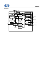
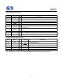
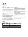
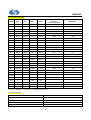
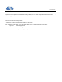
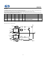
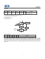
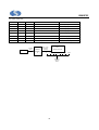
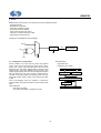
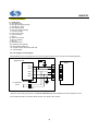
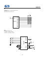
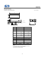
SH69P23
PRELIMINARY
OTP 4-bit Microcontroller
Features
SH6610C-based single-chip 4-bit micro-controller
OTPROM: 4K X 16 bits
RAM: 160 X 4 bits (data memory)
Operation voltage: 2.4V - 6.0V (typical 3.0V or 5.0V)
14 CMOS bi-directional I/O pins
Built in pull-up and pull-low resistor for PortA ~ PortF
4-level subroutine nesting (including interrupts)
One 8-bit auto re-load timer/counter
Warm-up timer for power on reset
Powerful interrupt sources:
- Internal interrupt (Timer0)
- External interrupts: PortB & PortC (rising/falling edge)
Oscillator (OTP option)
- X`tal oscillator:
32.768KHz - 4MHz
- Ceramic resonator: 400K - 4MHz
- RC oscillator: 400K - 4MHz
- External clock:
30K - 4MHz
Instruction cycle time:
- 4/32.768KHz(122us) for 32.768KHz OSC clock
- 4/4MHz (1us) for 4MHz OSC clock
Two low power operation modes: HALT and STOP
Built-in watch dog timer (OTP option)
Built-in power on reset
Two LPD level(OTP option)
- High level: 4.0V
- Low level:
2.5V
OTP type &Code protection
General Description
SH69P23 is a 4-bit micro controller. This chip integrates the SH6610C 4-bit CPU core with SRAM, 4K OTPROM, Timer and I/O
Ports.
Pin Configuration
1
20
PF0
2
19
PA1
PA3
3
18
PA0 / SDA
T0
4
17
OSCI / SCK
RESET/ VPP
5
16
OSCO
15
VDD
14
PC3
13
PC2
SH69P23
PF1
PA2
GND
6
PB0
7
PB1
8
PB2
9
12
PC1
PB3
10
11
PC0
1
V1.0
SH69P23
Block Diagram
RESET
OSCO
OSCI
OSC
WDTEN
CPU
RC
RESET
WATCHDOG
TIMER
PRESCLALER
PORTA ( 4-BITS )
PORTA [0:3]
Power
on
PORTB ( 4-BITS )
PORTB [0:3]
LPD
PORTC ( 4-BITS )
CTL REG.
PORTC [0:3]
LPDON
T0
8-BITS TIMER
( Up counter )
TIMER
INTERRUPT
PORTD (4-BITS )
OTPROM
4096*16 BITS
PORTF [0:1]
DATA RAM
160*4 BITS
2
SH69P23
Pin Description(Normail mode)
Pin No.
Designation
I/O
Descriptions
20, 1
PF[0:1]
I/O
Bit programmable I/O
18,19, 2, 3
PA[0:3]
I/O
Bit programmable I/O.
4
T0
I
Timer Clock/Counter input pin. (Schmitt trigger input)
5
RESET
I
Reset input (active low, Schmitt trigger input).
6
GND
P
Ground pin
7 - 10
PB[0:3]
I/O
Bit programmable I/O. Vector Interrupt (Active rising or falling edge by system
register setup)
11 - 14
PC[0:3]
I/O
Bit programmable I/O. Vector Interrupt (Active rising or falling edge by system
register setup)
15
VDD
P
Power supply pin
16
OSCO
O
OSC output pin. No output for RC mode
17
OSCI
I
OSC input pin, connected to a crystal, ceramic or external resistor.
Pin Description(OTP program mode)
Pin No.
Symbol
I/O
Shared by
Description
15
VDD
P
VDD
5
VPP
I
RESET
6
GND
P
GND
Ground
17
SCK
I
OSCI
Programming Clock input pin
18
SDA
I/O
PA[0]
Programming Data pin
Power supply (+5.5V)
High voltage Power supply (+10.5V)
* When the chip is being programmed, the VDD VPP SCK SDA should be separated from other appliction circuits .
3
SH69P23
Function Description
1. CPU
The CPU contains the following function blocks: Program
Counter, Arithmetic Logic Unit (ALU), Carry Flag,
Accumulator, Table Branch Register, Data Pointer (INX,
DPH, DPM, and DPL), and the Stack.
Decision (BA0, BA1, BA2, BA3, BAZ, BAC)
Logic Shift (SHR)
The Carry Flag (CY) holds the ALU overflow which the
arithmetic operation generates. During an interrupt servicing
or call instruction, the carry flag is pushed into the stack and
retrieved back from the stack by the RTNI instruction. It is
unaffected by the RTNW instruction.
1.1. PC (Program Counter)
The Program Counter is used to address the 4K program
ROM. It consists of 12-bits: the Page Register (PC11), and
the Ripple Carry Counter (PC10, PC9, PC8, PC7, PC6, PC5,
PC4, PC3, PC2, PC1, PC0).
The program counter normally increases by one (+1) with
every execution of an instruction except in the following
cases:
(1) When executing a jump instruction (such as JMP, BA0,
BAC),
(2) When executing a subroutine call instruction (CALL),
(3) When an interrupt occurs,
(4) When the chip is in the INITIAL RESET mode.
The program counter is loaded with data corresponding to
each instruction. The unconditional jump instruction (JMP)
can be set at 1-bit page register for higher than 2K.
1.3. Accumulator
The Accumulator is a 4-bit register holding the results of the
arithmetic logic unit. In conjunction with the ALU, data
transfer between the accumulator and system register or
data memory can be performed.
1.4. Stack
A group of registers are used to save the contents of CY &
PC (10-0) sequentially with each subroutine call or interrupt.
It is organized into 13 bits X 4 levels. The MSB is saved for
CY. 4 levels are the maximum allowed for subroutine calls
and interrupts.
The contents of the Stack are returned sequentially to the PC
with the return instructions (RTNI/RTNW). The stack is
operated on a first-in, last-out basis. This 4-level nesting
includes both subroutine calls and interrupts requests. Note
that program execution may enter an abnormal state if the
number of calls and interrupt requests exceed 4, and the
bottom of the stack will be shifted out.
1.2. ALU and CY
ALU performs arithmetic and logic operations. The ALU
provides the following functions:
Binary addition/subtraction (ADC, SBC, ADD, SUB, ADI,
SBI)
Decimal adjustment for addition/subtraction (DAA, DAS)
Logic operations (AND, EOR, OR, ANDIM, EORIM, ORIM)
2. OTPROM
The SH69P23 can address up to 4096 X 16 bit words of program area from $000 to $FFF.
Service routine as starting vector address.
Address
Instruction
$000H
JMP Instruction
$001H
NOP
$002H
JMP Instruction
$003H
NOP
$004H
JMP Instruction
Remarks
Jump to RESET service routine
Reserved
Jump to TIMER0 service routine
Reserved
Jump to PBC service routine
4
SH69P23
3. RAM
The built-in RAM consists of general-purpose data memory and the system register. Direct addressing in one instruction can
access both data memory and the system register.
The following is the memory allocation map:
$000 - $01F: System register and I/O.
$020 - $0BF: Data memory (160 X 4 bits, divided into 2 banks. $020 - $07F: bank0, $080 - $0BF: bank1).
(a). The Configuration of the System Register
Address
Bit3
Bit2
$00
-
IET0
$01
-
IRQT0
$02
-
TM0.2
$03
-
-
Bit1
Bit0
R/W
Remarks
-
IEP
R/W
Interrupt enable flags
-
IRQP
R/W
Interrupt request flags
TM0.1
TM0.0
R/W
-
-
-
Timer0 Mode register (Prescaler)
Reserved
$04
TL0.3
TL0.2
TL0.1
TL0.0
R/W
Timer0 load/counter register low digit
$05
TH0.3
TH0.2
TH0.1
TH0.0
R/W
Timer0 load/counter register high digit
$06-$07
-
-
-
-
-
$08
PA.3
PA.2
PA.1
PA.0
R/W
Reserved
PORTA
$09
PB.3
PB.2
PB.1
PB.0
R/W
PORTB
$0A
PC.3
PC.2
PC.1
PC.0
R/W
PORTC
Bit0-3 is reserved,Always keep it to “0”
in the User’s program.
Refer to I/O notice
$0B~$0C
$0D
-
-
PF.1
PF.0
R/W
PORTF
$0E
TBR.3
TBR.2
TBR.1
TBR.0
R/W
Table Branch Register
$0F
INX.3
INX.2
INX.1
INX.0
R/W
Pseudo index register
$10
DPL.3
DPL.2
DPL.1
DPL.0
R/W
Data pointer for INX low nibble
$11
-
DPM.2
DPM.1
DPM.0
R/W
Data pointer for INX middle nibble
DPH.2
DPH.1
DPH.0
R/W
Data pointer for INX high nibble
Reserved
Bit1:PBC interrupt rising / failing edge set
PH/PL
PBCFR
-
R/W
Bit2:Port pull-hi/low set
$12
$13 - $14
$15
PULLEN
Bit3: Port pull-up/low enable control
$16
PA3OUT PA2OUT PA1OUT PA0OUT
R/W
PortA input/output control 0: input
1: output
$17
PB3OUT PB2OUT PB1OUT PB0OUT
R/W
PortB input/output control 0: input
1: output
$18
PC3OUT PC2OUT PC1OUT PC0OUT
R/W
PortC input/output control 0: input
1: output
Bit0-3 is reserved,Always keep it to “1”
in the User’s program.
Refer to I/O notice
$19~$1A
$1B
-
-
PF1OUT
PF0OUT
R/W
$1C
-
-
T0S
T0E
$1D
-
-
-
-
-
$1E
WDT
-
-
-
W
$1F
-
-
-
-
-
PortF input/output control 0: input
Bit0: T0 signal edge;
Bit1: T0 signal source
R/W
1: output
Reserved
Bit3: WDT timer reset (write 1 to reset WDT)
Reserved
* System Register $00 - $12 (except $07H) refer to "SH6610C User manual".
5
SH69P23
(b) System Register state:
Power On Reset
/Pin Reset
/ Low Voltage Reset
Address
Bit 3
Bit 2
Bit 1
Bit 0
WDT Reset
$00
-
IET0
-
IEP
-0-0
-0-0
$01
-
IRQT0
-
IRQP
-0-0
-0-0
$02
-
TM0.2
TM0.1
TM0.0
- 000
- 000
$03
-
-
-
-
-
-
$04
TL0.3
TL0.2
TL0.1
TL0.0
0000
0000
$05
TH0.3
TH0.2
TH0.1
TH0.0
0000
0000
$06-$07
-
-
-
-
-
-
$08
PA.3
PA.2
PA.1
PA.0
1111
1111
$09
PB.3
PB.2
PB.1
PB.0
1111
1111
$0A
PC.3
PC.2
PC.1
PC.0
1111
1111
$0D
-
-
PF.1
PF.0
- -11
- -11
$0E
TBR.3
TBR.2
TBR.1
TBR.0
xxxx
uuuu
$0F
INX.3
INX.2
INX.1
INX.0
xxxx
uuuu
$10
DPL.3
DPL.2
DPL.1
DPL.0
xxxx
uuuu
$11
-
DPM.2
DPM.1
DPM.0
-xxx
-uuu
$12
-
DPH.2
DPH.1
DPH.0
-xxx
-uuu
$0B~$0C
$13 - $14
-
-
$15
PULLEN
PH/PL
PBCFR
-
010 -
010 -
$16
PA3OUT
PA2OUT
PA1OUT
PA0OUT
0000
0000
$17
PB3OUT
PB2OUT
PB1OUT
PB0OUT
0000
0000
$18
PC3OUT
PC2OUT
PC1OUT
PC0OUT
0000
0000
-
-
$19~$1A
$1B
-
-
PF1OUT
PF0OUT
- - 00
- - 00
$1C
-
-
T0S
T0E
- - 00
- - 00
$1D
-
-
-
-
-
-
$1E
WDT
-
-
-
-
-
$1F
-
-
-
-
-
-
Legend: x = unknown, u = unchanged, - = unimplemented read as '0'.
(c) Others initial state:
Others
After any Reset
Program Counter (PC)
$000
CY
Undefined
Accumulator (AC)
Undefined
Data Memory
Undefined
6
SH69P23
4. Low Power Detection (LPD)
The LPD function is used to monitor the supply voltage and applies an internal reset in the micro-controller at the time of battery
replacement. If the applied circuit satisfies the following conditions, the LPD can be incorporated using software control.
- Power supply voltage VDD = 2.4 to 6.0 V
4.1 Functions of the LPD Circuit
The LPD function is selected by OTP option.
The LPD circuit has the following functions:
- It generates an internal reset signal when VDD ≤ VLPD and t ≥ tLPD
- It cancels the internal reset signal when VDD > VLPD or VDD ≤ VLPD and t < tLPD
Here, VDD: power supply voltage, VLPD: LPD detect voltage, There are two level selected by OTP option:
Low level:
2.3~2.7V, typical 2.5V
High level:
3.8~4.2V, typical 4.0V
tLPD:
100us~500us, typical 300us
LPD can be enabled or disabled permanently by OTP option.
7
SH69P23
5. I/O Ports
The SH69P23 provides 14 I/O pins. When every I/O is used as an input port, the port control register controls ON/OFF of the
output buffer. Sections below show the circuit configuration of I/O ports.
Every I/O pin has a internal pull up / pull low resister, which is controled by PULLEN and PH/PL of $15
Each of these ports contains 4 or 2(PF) bits I/O pins. ON/OFF of the output buffer for port can be controlled by the port control
register. Port I/O mapping address is shown as follows:
Address
Bit3
Bit2
Bit1
Bit0
R/W
Remarks
Power On
$08
PA.3
PA.2
PA.1
PA.0
R/W
PORTA
1111
$09
PB.3
PB.2
PB.1
PB.0
R/W
PORTB
1111
$0A
PC.3
PC.2
PC.1
PC.0
R/W
PORTC
1111
Bit0-3 is reserved,Always keep it to “0”
in the User’s program.
$0B-$0C
$0D
PF.1
PF.0
R/W
PORTF
1111
Equivalent Circuit for a Single I/O Pin
VDD
PULL EN
AND
PH/PL
AND
VDD
DATA
D
Q
DATA
WRITE
CK
AND
QB
SET
RESET
I/O PIN
DATA IN
READ
CONTROL
WRITE
D
Q
PXXOUT
CK
RESET
QB
OR
GND
RESET
PULL EN
PH/PL
AND
AND
GND
8
SH69P23
System Register $16 - $1B
Address
Bit3
Bit2
Bit1
Bit0
R/W
$15
PULLEN
PH/PL
PBCFR
-
R/W
$16
PA3OUT
PA2OUT
PA1OUT
PA0OUT
W
PortA input/output control 0: input
1: output
0000
$17
PB3OUT
PB2OUT
PB1OUT
PB0OUT
W
PortB input/output control 0: input
1: output
0000
$18
PC3OUT
PC2OUT
PC1OUT
PC0OUT
W
PortC input/output control 0: input
1: output
0000
$19-$1A
$1B
Remarks
Power On
Bit1:PBC interrupt rising / failing edge set
Bit2:Port pull-hi/low set
Bit3: Port pull-up/low enable control
010 -
Bit0-3 is reserved,Always keep it to “1”
in the User’s program.
-
-
PF1OUT
PF0OUT
W
PortF input/output control 0: input
1: output
0000
* For SH69P23, after the chip reset, please first write 1111B to $19 $1A and write 0000B to $0B $0C . Otherwise, the halt
current and stop current will be abnormal
PAXOUT, PBXOUT, PCXOUT (X = 0, 1, 2, 3), PFXOUT (X = 0, 1)
1: Use as an output buffer
0: Use as an input buffer (Power on initial)
PBCFR:
1: Rising Edge interrupt
0: Falling Edge interrupt,
PH/PL:
1: Port Pull up resister ON,
0: Port Pull low resister ON,
PULLEN:
1: Port Pull up /Pull low enable,
0: Port Pull up /Pull low disable
9
SH69P23
PORTB & PORTC interrupt
The PORTB and PORTC are used as port interrupt sources. Since PORT I/O is bit programmable I/O, so only the input port can
generate an external interrupt.
When PBCFR set to 0, any one of the PORTB and PORTC input pin transitions from VDD to GND will generate an interrupt
request. And further falling edge transition would not be able to make interrupt request until all of the pins return to VDD.
When PBCFR set to 1, any one of the PORTB and PORTC input pin transitions from GND to VDD will generate an interrupt
request. And further rising edge transition would not be able to make interrupt request until all of the pins return to GND.
Following is the port interrupt function block-diagram.
PBOUT[3]
PB[3]
PBOUT[2]
PB[2]
PBOUT[1]
PB[1]
PBOUT[0]
PB[0]
PCOUT[3]
PC[3]
PCOUT[2]
PC[2]
PCOUT[1]
PC[1]
PCOUT[0]
PC[0]
PBCFR
PORT INTERRUPT
DETECT
PBOUT[3]
PB[3]
PBOUT[2]
PB[2]
PBOUT[1]
PB[1]
PBOUT[0]
PB[0]
PCOUT[3]
PC[3]
PCOUT[2]
PC[2]
PCOUT[1]
PC[1]
PCOUT[0]
PC[0]
10
PORTINT
SH69P23
6. T0 & WDT
System Register $1C
Address
BIT3
BIT2
BIT1
BIT0
R/W
$1C
-
-
T0S
T0E
W
Remark
Bit0: T0 signal edge
Bit1: T0 signal source
T0E: T0 signal edge
0: Increment on low-to-high transition T0 pin (Power on initial)
1: Increment on high-to-low transition T0 pin
T0S: T0 signal source.
0: OSC 1/4 (Power on initial).
1: Transition on T0 pin.
T0S
OSC/4
0
1
T0
M
U
X
TIMER0 (8bits)
EOR
TOE
3
Built-in RC
Oscillator
TM0 [2:0]
WDT Enable
(OTP option )
WDT & Warm
Up Counter
WDT reset
3
WDT Timeout
System Register $1E
Address
Bit3
Bit2
Bit1
Bit0
R/W
$1E
WDT
-
-
-
W
Remark
Bit3: Watchdog timer reset. (write 1 to reset WDT)
The input clock of the watchdog timer is generated by a built-in RC oscillator so that the WDT will always run even in the STOP
mode. SH69P23 generates a RESET condition when the watchdog times-out. The watchdog can be enabled or disabled
permanently by using the OTP option. To prevent it timing out and generating a device RESET condition, you should write this
bit as “1” before timing-out. The WDT has a time-out period of more than 7ms(typical 18ms) . If longer time-out periods are
desired, a prescaler with a division ratio of up to 1:2048 can be assigned to the WDT under software controll by writing to the
TM0 register.
11
SH69P23
Pre-scaler divide ratio:
TM0.2
TM0.1
TM0.0
1
1
1
1:1
Prescaler Divide Ratio
7ms(min)
Timer-out Period
1
1
0
1:2
14ms(min)
1
0
1
1:4
28ms(min)
1
0
0
1:8
56ms(min)
0
1
1
1:32
224ms(min)
0
1
0
1:128
896ms(min)
0
0
1
1:512
3,584ms(min)
0
0
0
1:2048 (Power on initial)
14,336ms(min)
0.875ms
(min)
RC OSC
Internal
WDT Time
out Period
7ms(min)
WDT
PRESCALER TM0
SCALER_1
/8
/1
/2
/4
/8
/32 /128
Final WDT
Time out
period
12
/512
/2048
SH69P23
7. Timer0
SH69P23 has one 8-bit timer. The time/counter has the following features:
. 8-bit timer/counter
. Readable and writeable
. Automatic reloadable counter
. 8-prescaler scale is available
. Internal and external clock select
. Interrupt on overflow from $FF to $00
. Edge select for external event
Following is a simplified timer block diagram:
Fosc/4
PRE-SCALER
T0C
8-BIT COUNTER
T0
T0M
T0E
T0S
Read Operation:
7.1. Configuration and Operation
High nibble first;
Followed by Low nibble.
Timer0 consists of an 8-bit write-only timer load register
(TL0L, TL0H), and an 8-bit read-only timer counter (TC0L,
TC0H). The counter and load register both have low order
digits and high order digits. Writing data into the timer load
register (TL0L, TL0H) can initialize the timer counter. Load
register programming: Write the low-order digit first and then
the high-order digit. The timer counter is loaded with the
contents of the load register automatically when the high
order digit is written or the counter counts overflow from $FF
to $00.
Timer Load Register: Since the register H controls the
physical READ and WRITE operation, please follow these
rules:
Write Operation:
First write Low nibble,
Then write High nibble to update the counter.
Load Reg. L
Load Reg. H
8-bit timer counter
Latch Reg. L
13
SH69P23
7.2. Timer0 Interrupt
The timer overflow will generate an internal interrupt request, when the counter counts overflow from $FF to $00. If the interrupt
enable flag is enabled, then a timer interrupt service routine will proceed. This can also be used to waken the CPU from HALT
mode.
7.3. Timer0 Mode Register
The timer can be programmed in several different prescaler ratios by setting the Timer Mode register (TM0). The 8-bit counter
counts prescaler overflow output pulses. The timer mode registers (TM0) are 3-bit registers used for timer control as shown in
table1. These mode registers select the input pulse sources into the timer.
Table 1. Timer 0 Mode Register ($02)
TM0.2
TM0.1
0
0
0
0
0
1
0
1
1
0
1
0
1
1
1
1
TM0.0
Prescaler Divide Ratio
0
2048 (initial)
9
512
7
128
5
32
3
8
4
4
1
2
0
1
/2
1
/2
0
/2
1
/2
0
/2
1
/2
0
/2
1
Ratio N
11
/2
7.4. External Clock/Event T0 as Timer0 Source
When an external clock/event input is used for the TM0, it is synchronized with the CPU system clock. Therefor the external
source must follow certain constraints. The output from the T0M multiplex is T0C. It is sampled by the system clock in instruction
frame cycle. Therefore it is necessary for the T0C to be high (at least 2 tOSC) and low (at least 2 tOSC). When the prescaler ratio
0
selects /2 , the T0C is the same as the system clock input. Therefore the requirement is as follows
T0H = T0CH = T0 high time ≥ 2 tOSC + ∆T
T0L = T0CL = T0 low time ≥ 2 tOSC + ∆T
Note: ∆T = 40ns
When another prescaler ratio is selected, the TM0 is scaled by the asynchronous ripple counter and so the prescaler output is
symmetrical.
Then:
T0C high time = T0C low time =
N * T0
2
Where
T0 = Timer0 input period
N = prescaler value
The requirement is, therefore:
4 * t OSC + 2ΔT
N * T0
≥ 2 tOSC + ∆T , or T0 ≥
N
2
The limitation is applied for the T0 period time only. The pulse width is not limited by this equation. It is summarized as follows:
T0 = Timer0 period ≥
4 * t OSC + 2∆T
N
14
SH69P23
8. System Clock and Oscillator
System clock generator produces the basic clock pulses that provide the system clock to the CPU and any peripherals.
Instruction cycle time
(1) 4/32.768KHz (≈122us) for 32.768KHz system clock
(2) 4/4MHz (1us) for 4MHz system clock
8.1 Oscillator
(1) Crystal oscillator: 32.768KHz – 4MHz.
OSCI
C1
Crystal
32.768K - 4MHz
OSCO
C2
(2) Ceramic resonator: 400KHz – 4MHz.
C1
OSCI
Ceramic
400K - 4MHz
OSCO
C2
(3) RC oscillator: 400KHz – 4MHz.
VDD
R
OSCI
C1 = 1000p
OSCO
(4) External input clock: 30KHz – 4MHz.
OSCI
External clock source
OSCO
15
SH69P23
9. OTP Program Notice:
9.1. OTP option
(a). Oscillator range
0: OSC @ 32K~2MHz (default)
1: OSC @ 2M ~ 4MHz
(b). LPD voltage range
0: High LPD voltage (default)
1: Low LPD Voltage
(c): LPD on/off control
0: LPD off (default)
1: LPD on
(d): WDT on/off control
0: WDT on (default)
1: WDT off
(e): Oscillator select:
000: External clock (default)
100: RC Oscillator 400k~4M
110: Crystal /Ceramic Resonator 400k~4M
111: X’tal 32768Hz
9.2. OTP Program circuit diagram
If the SH69P23 need to be programed in circuit, the program interface can be connect as the following diagram.
VDD
Application PCB
OTP
Writer
SH6XPXX
VPP
VDD
SCK
SDA
GND
To application
circuit
Jumper
* When the chip is being programmed, the VDD VPP SCK SDA should be separated from other appliction circuits .
If more detail information is needed, please see the “OTP writer’s user manual”.
16
SH69P23
Instruction Set
All instructions are one cycle and one-word instructions. The characteristic is memory-oriented operation.
Arithmetic and Logical Instruction
Accumulator Type
Mnemonic
Instruction Code
Function
Flag Change
ADC
X (, B)
00000 0bbb xxx xxxx
AC
← Mx + AC + CY
CY
ADCM
X (, B)
00000 1bbb xxx xxxx
AC, Mx ← Mx + AC + CY
CY
ADD
X (, B)
00001 0bbb xxx xxxx
AC
ADDM
X (, B)
00001 1bbb xxx xxxx
AC, Mx ← Mx + AC
SBC
X (, B)
00010 0bbb xxx xxxx
AC
← Mx + -AC + CY
CY
SBCM
X (, B)
00010 1bbb xxx xxxx
AC, Mx ← Mx + -AC + CY
CY
SUB
X (, B)
00011 0bbb xxx xxxx
AC
← Mx + -AC + 1
CY
SUBM
X (, B)
00011 1bbb xxx xxxx
AC, Mx ← Mx + -AC + 1
CY
EOR
X (, B)
00100 0bbb xxx xxxx
AC
EORM
X (, B)
00100 1bbb xxx xxxx
AC, Mx ← Mx ⊕ AC
OR
X (, B)
00101 0bbb xxx xxxx
AC
ORM
X (, B)
00101 1bbb xxx xxxx
AC, Mx ← Mx | AC
AND
X (, B)
00110 0bbb xxx xxxx
AC
ANDM
X (, B)
00110 1bbb xxx xxxx
AC, Mx ← Mx & AC
SHR
11110 0000 000 0000
← Mx + AC
CY
CY
← Mx ⊕ AC
← Mx | AC
← Mx & AC
0 → AC[3]; AC[0] →CY;
AC shift right one bit
CY
Immediate Type
Mnemonic
Instruction Code
Function
Flag Change
ADI
X, I
01000 iiii xxx xxxx
AC
← Mx + I
CY
ADIM
X, I
01001 iiii xxx xxxx
AC, Mx ← Mx + I
CY
SBI
X, I
01010 iiii xxx xxxx
AC
SBIM
X, I
01011 iiii xxx xxxx
AC, Mx ← Mx + -I + 1
EORIM
X, I
01100 iiii xxx xxxx
AC, Mx ← Mx ⊕ I
ORIM
X, I
01101 iiii xxx xxxx
AC, Mx ← Mx | I
ANDIM
X, I
01110 iiii xxx xxxx
AC, Mx ← Mx & I
← Mx + -I +1
CY
CY
In the assembler ASM66 V1.0, the EORIM mnemonic is EORI. However, EORI has the identical operation to EORIM.
The same is true for the ORIM with respect to ORI, and ANDIM with respect to ANDI.
Decimal Adjustment
Mnemonic
Instruction Code
Function
Flag Change
DAA X
11001 0110 xxx xxxx
AC; Mx ← Decimal adjustment for add.
CY
DAS X
11001 1010 xxx xxxx
AC; Mx ← Decimal adjustment for sub.
CY
17
SH69P23
Transfer Instructions
Mnemonic
Instruction Code
LDA
X (, B)
00111 0bbb xxx xxxx
AC
← Mx
STA
X (, B)
00111 1bbb xxx xxxx
Mx
← AC
LDI
X, I
01111 iiii xxx xxxx
AC, Mx ← I
Function
Flag Change
Function
Flag Change
Control Instructions
Mnemonic
Instruction Code
BAZ X
10010 xxxx xxx xxxx
PC
← X if AC = 0
BNZ X
10000 xxxx xxx xxxx
PC
← X if AC ≠ 0
BC X
10011 xxxx xxx xxxx
PC
← X if CY = 1
BNC X
10001 xxxx xxx xxxx
PC
← X if CY ≠ 1
BA0 X
10100 xxxx xxx xxxx
PC
← X if AC(0) = 1
BA1 X
10101 xxxx xxx xxxx
PC
← X if AC(1) = 1
BA2 X
10110 xxxx xxx xxxx
PC
← X if AC(2) = 1
BA3 X
10111 xxxx xxx xxxx
PC
← X if AC(3) = 1
CALL X
11000 xxxx xxx xxxx
ST
← CY; PC + 1
PC
← X (Not including p)
RTNW H, L
11010 000h hhh llll
PC
←ST; TBR ← hhhh;
AC
← llll
RTNI
11010 1000 000 0000
HALT
11011 0000 000 0000
STOP
11011 1000 000 0000
JMP X
1110p xxxx xxx xxxx
PC
← X (Including p)
TJMP
11110 1111 111 1111
PC
← (PC11-PC8) (TBR) (AC)
NOP
11111 1111 111 1111
No Operation
CY; PC ← ST
CY
Where,
PC
Program counter
I
Immediate data
AC
Accumulator
⊕
Logical exclusive OR
-AC
Complement of accumulator
|
Logical OR
CY
Carry flag
&
Logical AND
Mx
Data memory
p
ST
bbb
ROM page
B
Stack
TBR
18
RAM bank
RAM bank.
Every $7F as one RAM bank.
Table Branch Register
SH69P23
Absolute Maximum Rating*
*Comments
DC Supply Voltage . . . . . . . . . . . . . . –0.3V to + 7.0V
Stresses above those listed under “Absolute Maximum
Ratings” may cause permanent damage to this device.
These are stress ratings only. Functional operation of this
device under these or any other conditions above those
indicated in the operational sections of this specification is
not implied or intended. Exposure to the absolute maximum
rating conditions for extended periods may affect device
reliability.
Input Voltage . . . . . . . . . . . . . . . –0.3V to VDD + 0.3V
Operating Ambient Temperature . . . –40℃ to + 85℃
Storage Temperature . . . . . . . . . . .-55℃ to + 125℃
DC Electrical Characteristics (VDD = 5.0V GND = 0V, TA = 25℃, FOSC = 4MHz, unless otherwise specified)
Parameter
Symbol
Min.
Typ.
Max.
Unit
Operating Voltage
VDD
4.5
5.0
6.0
V
Operating Current
IOP
0.6
1.0
mA
Stand by Current (HALT)
ISB1
0.5
mA
Stand by Current (STOP)
ISB2
1
µA
Input Low Voltage
VIL1
GND
0.2 X VDD
V
LPD off (If LPD on, ISB2X = ISB2 + 2µA)
WDT off (If WDT on, ISB2X = ISB2 + 15µA)
I/O ports, pins tri-state
Input Low Voltage
VIL2
GND
0.15 X VDD
V
RESET , T0
Input Low Voltage
Input High Voltage
VIL3
VIH1
GND
0.8 X VDD
0.15 X VDD
VDD
V
V
OSCI (Driven by external clock)
I/O ports, pins tri-state
Input High Voltage
VIH2
0.85 X VDD
VDD
V
RESET , T0
Input High Voltage
VIH3
0.85 X VDD
VDD
V
OSCI (Driven by external Clock)
Input Leakage Current
IIL1
-1
1
µA
I/O ports, GND < VI/O < VDD
Input Leakage Current
IIL2
-5
Input Leakage Current
IIL3
Input Leakage Current
IIL4
Input Leakage Current
IIL5
Pull-up/ Pull-low Resistor
RP
VOH
Output Low Voltage
VOL
All output pins unloaded
(Execute NOP instruction)
All output pins unloaded
All output pins unloaded,
µA
V RESET = GND + 0.25V
1
5
µA
V RESET = VDD
-3
1
3
µA
T0, GND < Vt0 < VDD
-3
1
3
µA
For OSCI
KΩ
150
Output High Voltage
Condition
VDD – 0.7
V
GND + 0.6
V
PULL-UP/ PULL-LOW resistor
I/O ports, IOH = -10mA
OSCORC, IOH = -0.7mA
I/O ports, IOL = 20mA
OSCORC, IOL = 1.6mA
AC Electrical Characteristics (VDD = 5.0V GND = 0V, TA = 25℃, unless otherwise specified)
Parameter
Symbol
Oscillator Start Time
RESET pulse width (low)
WDT Period
TOSC1
TRESET
Twdt
Frequency Stability (RC)
∆ F/F
Min.
10
7
Typ.
Max.
Unit
1
s
µs
ms
X’tal osc = 32.768KHz
VDD = 5.0V
VDD = 5.0V
20
%
RC Oscillator: [F(5.0)-F(4.5)]/F(5.0)
18
19
Condition
SH69P23
DC Electrical Characteristics (VDD = 3.0V, GND = 0V, TA = 25℃, FOSC = 4MHz, unless otherwise specified)
Symbol
Min.
Typ
.
Max.
Unit
Operating Voltage
VDD
2.4
3.0
4.5
V
Operating Current
IOP
0.3
0.6
mA
All output pins unloaded
(Execute NOP instruction)
Stand by Current (HALT)
ISB1
0.2
mA
All output pins unloaded
Stand by Current (STOP)
ISB2
1
µA
Input Low Voltage
VIL1
GND
0.2 X VDD
V
LPD off (If LPD on, ISB2X = ISB2 + 2µA)
WDT off (If WDT on, ISB2X = ISB2 + 5µA)
I/O ports, pins tri-state
Input Low Voltage
VIL2
GND
0.15 X VDD
V
Input Low Voltage
VIL3
GND
0.15 X VDD
V
RESET , T0
OSCI (Driven by external clock)
Input High Voltage
VIH1
0.8 X VDD
VDD
V
I/O ports, pins tri-state
Input High Voltage
VIH2
0.85 X VDD
VDD
V
Input High Voltage
VIH3
0.85 X VDD
VDD
V
RESET , T0
OSCI (Driven by external Clock)
Input Leakage Current
IIL1
-1
1
µA
I/O ports, GND < Vi/o < VDD
Input Leakage Current
IIL2
-5
µA
V RESET = GND + 0.25V
Input Leakage Current
IIL3
Input Leakage Current
IIL4
Input Leakage Current
IIL5
Output High Voltage
VOH
VDD – 0.7
Output Low Voltage
VOL
Parameter
Condition
All output pins unloaded,
1
5
µA
V RESET = VDD
-3
1
3
µA
T0, GND < Vt0 < VDD
-3
1
3
µA
For OSCI
V
I/O ports, IOH = -7mA, VDD = 3V
OSCORC, IOH = -0.7mA, VDD = 3V
V
I/O ports, IOL = 8mA, VDD = 3V
OSCORC, IOL = 1.0mA, VDD = 3V
GND + 0.4
User Notice:
Max. Current into VDD = 50mA;
Max. Current out of VSS = 150mA
Max. Output current sunk by any I/O port = 25mA;
Max. Output current sourced by any I/O port = 20mA
Max. Output current sunk by all ports (A, B, C, D, E, F) = 50mA;
Max. Output current sourced by all ports (A, B, C, D, E, F) = 40mA
AC Electrical Characteristics (VDD = 3.0V, GND = 0V, TA = 25℃, unless otherwise specified)
Parameter
Oscillator Start Time
Symbol
Min.
TOSC1
TRESET
12
WDT Period
TWDT
7
Frequency Stability (RC)
∆ F/F
RESET pulse width (low)
Typ
.
Max.
Unit
1
s
Crystal Osc = 32.768KHz, VDD = 3.0V
µs
VDD = 3.0V
ms
VDD = 3.0V
%
RC oscillator (1MHz): [F(3.0)-F(2.7)]/F(3.0)
18
20
Condition
Low Power Detect Electrical Characteristics
(a) VDD = 2.4~6V, GND = 0V, TA = 25°C, FOSC = 4MHz, unless otherwise specified.
Parameter
LPD Voltage(Low)
Symbol
Min.
Typ
.
Max.
Unit
VLPD1
2.3
2.5
2.7
V
20
Condition
LPD enable
SH69P23
LPD Voltage(High)
Low power detect ignore time
VLPD2
3.8
4.0
4.2
V
tLPD
100
300
500
us LPD enable and VDD<VLPD
21
LPD enable
SH69P23
AC Characteristics
Symbol
Parameter
Min.
TCY
Instruction Cycle Time
1
Typ.
Max.
Unit
122
µs
TIW
T0 Input Width
(TCY + 40)/N
ns
TIWH
High Pulse Width
1/2 tIW
ns
TIWL
LOW Pulse Width
1/2 tIW
ns
Timing Waveform
T0 Input Waveform
TiwH
TiwL
T0
Tiw
Built-in RC Oscillator (Only use for Watch Dog)
RESET
OSC
WDT
Built-in RC
Tosc1
Twdt
22
Condition
N = Prescaler divide ratio
SH69P23
Typical RC oscillator Resistor vs. Frequency: (VDD = 5V, for reference only)
5V RC Frequency
Fosc(kHz)
10000.00
1000.00
100.00
0.00
50.00
100.00
150.00
200.00
250.00
300.00
350.00
400.00
R(k om)
Typical RC Oscillator Resistor vs. Frequency: (VDD = 3V, for reference only)
3V RC Frequancy
Fosc(k Hz)
10000.00
1000.00
100.00
0.00
50.00
100.00
150.00
200.00
250.00
R(k om)
23
300.00
350.00
400.00
SH69P23
Application Circuit (for reference only)
AP1
(1) Operating voltage: 5.0V
(2) Oscillator: Ceramic resonator 455KHz
(3) T0 input timer clock / counter
(4) PORTA - F: I/O
T0
OSCI
VDD
20P
SH69P23
47K Ω
OSCO
RESET
C1
PORTA
~
PORTC
PORTF
0.1u
GND
I/O
AP2
(1) Operating voltage: 5.0V.
(2) Oscillator: RC 420KHz.
(3) PORTA – C,F: I/O
VDD
OSCI
22KΩ
47KΩ
T0
C1
0.1u
SH69P25
OSCO
RESET
PORTA
~
PORTF
GND
24
1000PF
I/O
SH69P23
AP3
(1) PORTA - C: as scan KEY BOARD (32 keys)
(2) PORTF: I/O,
(3) All input pin internal Pull up On
I/O
PORTF
SH69P23
PC0
PC1
PC2
PC3
PB0
PB1
PB2
PB3
PA0
PA1
PA2
PA3
AP4:
a. Operating voltage: 3.0V.
b. Oscillator: Crystal 32.768KHz.
c. PORTA - C: I/O. (PULL UP ON)
PA.0
PC.0
PC.1
PC.2
PC.3
PA.1
PA.2
PA.3
SH69P23
PB.0
PB.1
PB.2
I/O
10KΩ
RESET
0.1uF
PB.3
T0
OSCI
VDD
OSCO
GND
25
20p
20p
SH69P23
Ordering Information
Part No.
Packages
SH69P23
20L DIP
SH69P23M
20L SOP
26
SH69P23
Package Information
unit: inches/mm
P-DIP 20L Outline Dimensions
D
11
E1
20
1
10
E
A1
A2
Base Plane
Seating Plane
L
A
C
S
B
e1
B1
α
Symbol
Dimensions in inches
Dimensions in mm
A
0.175 Max.
4.45 Max.
A1
0.010 Min.
0.25 Min.
A2
0.130 ± 0.010
3.30 ± 0.25
B
0.018 +0.004
-0.002
0.46 +0.10
-0.05
B1
0.060 +0.004
-0.002
1.52 +0.10
-0.05
C
0.010 +0.004
-0.002
0.25 +0.10
-0.05
D
1.026 Typ. (1.046 Max.)
26.06 Typ. (26.57 Max.)
E
0.300 ± 0.010
7.62 ± 0.25
E1
0.250 Typ. (0.262 Max.)
6.35 Typ. (6.65 Max.)
e1
0.100 ± 0.010
2.54 ± 0.25
L
0.130 ± 0.010
3.30 ± 0.25
α
0° ~ 15°
0° ~ 15°
eA
0.345 ± 0.035
8.76 ± 0.89
S
0.078 Max.
1.98 Max.
Notes:
1. The maximum value of dimension D includes end flash.
2. Dimension E1 does not include resin fins.
3. Dimension S includes end flash.
27
eA
SH69P23
unit: inches/mm
SOP 20L (W.B.) Outline Dimensions
20
11
e1
HE
E
~
~
θ
L
1
10
Detail F
e1
e
Seating Plane
D
S
b
A
LE
A1
A2
c
D
y
See Detail F
Symbol
Dimensions in inches
Dimensions in mm
A
0.106 Max.
2.69 Max.
A1
0.004 Min.
0.10 Min.
A2
0.092 ± 0.005
2.33 ± 0.13
b
0.016 +0.004
-0.002
0.41 +0.10
-0.05
C
0.010 +0.004
-0.002
0.25 +0.10
-0.05
D
0.500 ± 0.02
12.80 ± 0.51
E
0.295 ± 0.010
7.49 ± 0.25
e
0.050 ± 0.006
1.27 ± 0.15
e1
0.376 NOM.
9.50 NOM.
HE
0.406 ± 0.012
10.31 ± 0.31
L
0.032 ± 0.008
0.81 ± 0.20
LE
0.055 ± 0.008
1.40 ± 0.20
S
0.042 Max.
1.07 Max.
y
0.004 Max.
0.10 Max.
θ
0° ~ 10°
0° ~ 10°
Notes:
1. The maximum value of dimension D includes end flash.
2. Dimension E does not include resin fins.
3. Dimension e1 is for PC Board surface mount pad pitch design
reference only.
4. Dimension S includes end flash.
28
SH69P23
Product Spec. Change Notice
SH69P23 Specification Revision History
Version
1.0
0.1
Content
Reduce operating current.
Add RC Frequency-Resistance diagram.
Original
29
Date
May.2003
Mar.2003