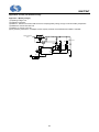
1
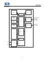
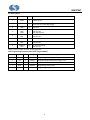
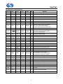
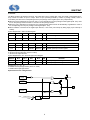
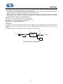
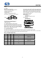
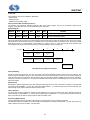
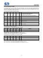
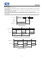
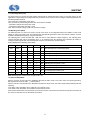
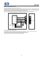
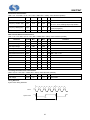
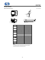
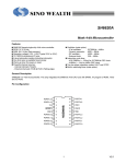
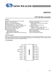
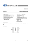
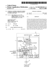
SH67P847 OTP 1K 4-bit micro-controller with 10-bit SAR ADC Features SH6610C-Based Single-Chip 4-bit Micro-Controller With 10-bit SAR ADC OTP ROM: 1K X 16bits RAM: 124 X 4bits - 28 System Control Registers - 96 Data Memory Operation Voltage: - fOSC = 16MHz, VDD = 3.3V - 5.5V 6 CMOS Bi-Directional I/O Pins 4-Level Stack (Including Interrupts) One 8-bit Auto Re-Loaded Timer Warm-Up Timer Powerful Interrupt Sources: - A/D Interrupt - Timer0 Interrupt - External Interrupts: PORTA.3 (Falling Edge) Oscillator - Internal RC Oscillator: 16MHz Instruction Cycle Time (16/fOSC) Two Low Power Operation Modes: HALT And STOP Reset - Built-in Power-on Reset (POR) - Built-in Low Voltage Reset (LVR) (Code Option) - Built-in Watchdog Timer (WDT) (Code Option) 4 Channels 10-bit Resolution Analog/Digital Converter (ADC) 1 Channels 9-bit PWM Output OTP Type/Code Protection 8-pin SOP package available General Description SH67P847 is a single-chip 4-bit micro-controller. This device integrates a SH6610C CPU core, RAM, ROM, timer, ADC, high speed PWM output, watch dog timer, low voltage reset. The SH67P847 is suitable for charger application. Pin Configuration 1 PORTA.3/VPP 2 GND 3 PORTA.0/VREF/AN0/SDA 4 SH67P847 PORTB.1/PWM 1 8 PORTB.0/AN3 7 PORTA.2/AN2/SCK 6 VDD 5 PORTA.1/AN1 V2.0 SH67P847 Block Diagram Reset Circuit Oscillator Watchdog Timer RAM 28 X 4 Bits System Register RAM 96 X 4 Bits Data Memory PORTA (4-Bit) PORTA.0/AN0/VREF PORTA.1/AN1 PORTA.2/AN2 PORTA.3/VPP PORTB (4-Bit) PORTB.0/AN3 PORTB.1/PWM ADC OTP ROM 1024 X 16 Bits PWM CPU Timer VDD Power Circuit GND 2 SH67P847 Pin Descriptions Pin No. Pin Name I/O Description 1 PORTB.1 /PWM I/O O Bit programmable I/O PWM output pin 2 PORTA.3 - I/O I Bit programmable I/O (Open drain type) Vector Interrupt. (Active falling edge) 3 GND P 4 PORTA.0 /AN0 /VREF I/O I I Bit programmable I/O ADC input pin ADC VREF input pin 5 PORTA.1 /AN1 I/O I Bit programmable I/O ADC input pin 6 VDD P 7 PORTA.2 /AN2 I/O Bit programmable I/O ADC input pin 8 PORTB.0 /AN3 I/O I Bit programmable I/O ADC input pin Ground pin Power supply pin Which, I: Input; O: Output; P: Power; Z: High impedance OTP Programming Pin Description (OTP Program Mode) Pin No. Symbol I/O Sharing Pin Description 6 VDD P VDD 2 VPP P PORTA.3 3 GND P GND 7 SCK I PORTA.2 Programming clock input pin 4 SDA I/O PORTA.0 Programming data pin Programming power supply (+5.5V) Programming high voltage power supply (+11V) Ground Which, I: Input; O: Output; P: Power; Z: High impedance 3 SH67P847 Functional Description 1. CPU The CPU contains the following functional blocks: Program Counter (PC), Arithmetic Logic Unit (ALU), Carry Flag (CY), Accumulator, Table Branch Register, Data Pointer (INX, DPH, DPM, and DPL) and Stacks. 1.1. PC The PC is used for ROM addressing consisting of 12-bit: Page Register (PC11), and Ripple Carry Counter (PC10, PC9, PC8, PC7, PC6, PC5, PC4, PC3, PC2, PC1, PC0). The program counter is loaded with data corresponding to each instruction. The unconditional jump instruction (JMP) can be set at 1-bit page register for higher than 2K. The program counter cans only 4K program ROM address. (Refer to the ROM description). 1.2. ALU and CY The ALU performs arithmetic and logic operations. The ALU provides the following functions: Binary addition/subtraction (ADC, SBC, ADD, SUB, ADI, SBI) Decimal adjustments for addition/subtraction (DAA, DAS) Logic operations (AND, EOR, OR, ANDIM, EORIM, ORIM) Decisions (BA0, BA1, BA2, BA3, BAZ, BNZ, BC, BNC) Logic Shift (SHR) The Carry Flag (CY) holds the ALU overflow that the arithmetic operation generates. During an interrupt service or CALL instruction, the carry flag is pushed into the stack and recovered from the stack by the RTNI instruction. It is unaffected by the RTNW instruction. 1.3. Accumulator (AC) The accumulator is a 4-bit register holding the results of the arithmetic logic unit. In conjunction with the ALU, data is transferred between the accumulator and system register, or data memory can be performed. 1.4. Table Branch Register (TBR) Table Data can be stored in program memory and can be referenced by using Table Branch (TJMP) and Return Constant (RTNW) instructions. The TBR and AC are placed by an offset address in program ROM. TJMP instruction branch into address ((PC11 - PC8) X (28) + (TBR, AC)). The address is determined by RTNW to return look-up value into (TBR, AC). ROM code bit7-bit4 is placed into TBR and bit3-bit0 into AC. 1.5. Data Pointer The Data Pointer can indirectly address data memory. Pointer address is located in register DPH (3-bit), DPM (3-bit) and DPL (4-bit). The addressing range can have 3FFH locations. Pseudo index address (INX) is used to read or write Data memory, then RAM address Bit9-0 which comes from DPH, DPM and DPL. 1.6. Stack The stack is a group of registers used to save the contents of CY & PC (11-0) sequentially with each subroutine call or interrupt. The MSB is saved for CY and it is organized into 13 bits X 4 levels. The stack is operated on a first-in, last-out basis and returned sequentially to the PC with the return instructions (RTNI/RTNW). Note: The stack nesting includes both subroutine calls and interrupts requests. The maximum allowed for subroutine calls and interrupts are 4 levels. If the number of calls and interrupt requests exceeds 4, then the bottom of stack will be shifted out, that program execution may enter an abnormal state. 2. RAM Built-in RAM contains general-purpose data memory and system register. Because of its static nature, the RAM can keep data after the CPU entering STOP or HALT. 2.1. RAM Addressing Data memory and system register can be accessed in one instruction by direct addressing. The following is the memory allocation map: System register: $000 - $01F Data memory: $020 - $07F 4 SH67P847 2.2. Configuration of System Register Address Bit 3 Bit 2 Bit 1 Bit 0 R/W Remarks $00 IEAD IET0 - IEP R/W Interrupt enable flags register $01 IRQAD IRQT0 - IRQP R/W Interrupt request flags register $02 - T0M.2 T0M.1 T0M.0 R/W Bit2-0: Timer0 Mode register $03 T0L.3 T0L.2 T0L.1 T0L.0 R/W Timer0 load/counter low nibble register $04 T0H.3 T0H.2 T0H.1 T0H.0 R/W Timer0 load/counter high nibble register $05 PA.3 PA.2 PA.1 PA.0 R/W PORTA data register $06 - - PB.1 PB.0 R/W PORTB data register $07 VREFS CH1 CH0 ADCON $08 ACR3 ACR2 ACR1 ACR0 R/W Bit3 - 0: ADC port configuration register $09 GO/ DONE TADC1 TADC0 ADCS Bit0: ADC conversion time control register R/W Bit1-0: ADC clock period control register Bit3: ADC status flag register $0A A2 A1 A0 - Bit0: ADC module operate control register R/W Bit2-1: ADC channel control register Bit3: ADC reference voltage control register R ADC data low nibble register $0B A6 A5 A4 A3 R ADC data medium nibble register $0C - A9 A8 A7 R ADC data high nibble register $0D - - - - $0E TBR.3 TBR.2 TBR.1 TBR.0 R/W Table Branch register $0F INX.3 INX.2 INX.1 INX.0 R/W Pseudo index register $10 DPL.3 DPL.2 DPL.1 DPL.0 R/W Data pointer for INX low nibble register $11 - DPM.2 DPM.1 DPM.0 R/W Data pointer for INX middle nibble register $12 - DPH.2 DPH.1 DPH.0 R/W Data pointer for INX high nibble register $13 PACR.3 PACR.2 PACR.1 PACR.0 R/W PORTA input/output control register $14 - - PBCR.1 PBCR.0 R/W PORTB input/output control register $15 PWMS TCK1 TCK0 $16 PP.3 PP.2 PP.1 PP.0 R/W PWM period low nibble register $17 PP.7 PP.6 PP.5 PP.4 R/W PWM period high nibble register $18 - - - PDF.0 R/W PWM duty fine tune register $19 PD.3 PD.2 PD.1 PD.0 R/W PWM duty low nibble register $1A PD.7 PD.6 PD.5 PD.4 R/W PWM duty high nibble register $1B - PPACR.2 PPACR.1 PPACR.0 $1C - - PPBCR.1 PPBCR.0 R/W PORTB pull-high control register $1D - - - - $1E WDT WDT.2 - WDT.1 - WDT.0 - $1F - - - - R/W Reserved Bit0: PWM output control register PWM_EN R/W Bit2-1: PWM clock source control register Bit3: PWM output mode control register R/W PORTA pull-high control register - Reserved R/W Bit2-0: Watchdog timer control register R Bit3: WDT overflow flag register - 5 Reserved SH67P847 3. ROM The ROM can address 1024 X 16 bits of program area from $000 to $3FF. 3.1. Vector Address Area ($000 to $004) The program is sequentially executed. There is an area address $000 through $004 that is reserved for a special interrupt service routine such as starting vector address. Address Instruction Remarks $000 JMP* Jump to RESET service routine $001 JMP* Jump to ADC interrupt service routine $002 JMP* Jump to TIMER0 interrupt service routine $003 JMP* - $004 JMP* Jump to Port interrupt service routine *JMP instruction can be replaced by any instruction. 6 SH67P847 4. Initial State 4.1. System Register State Address Bit 3 Bit 2 Bit 1 Power-on Reset /Low Voltage Reset Bit 0 WDT Reset $00 IEAD IET0 - IEP 00-0 00-0 $01 IRQAD IRQT0 - IRQP 00-0 00-0 $02 - T0M.2 T0M.1 T0M.0 -000 -uuu $03 T0L.3 T0L.2 T0L.1 T0L.0 xxxx xxxx $04 T0H.3 T0H.2 T0H.1 T0H.0 xxxx xxxx $05 PA.3 PA.2 PA.1 PA.0 0000 0000 $06 - - PB.1 PB.0 --00 --00 $07 VREFS CH1 CH0 ADCON 0000 uuuu $08 ACR3 ACR2 ACR1 ACR0 0000 uuuu $09 GO/ DONE A2 TADC1 TADC0 ADCS 0000 0uuu $0A A1 A0 - xxxx uuuu $0B A6 A5 A4 A3 xxxx uuuu $0C - A9 A8 A7 -xxx -uuu $0D - - - - ---- ---- $0E TBR.3 TBR.2 TBR.1 TBR.0 xxxx uuuu $0F INX.3 INX.2 INX.1 INX.0 xxxx uuuu $10 DPL.3 DPL.2 DPL.1 DPL.0 xxxx uuuu $11 - DPM.2 DPM.1 DPM.0 -xxx -uuu $12 - DPH.2 DPH.1 DPH.0 -xxx -uuu $13 PACR.3 PACR.2 PACR.1 PACR.0 0000 0000 $14 - - PBCR.1 PBCR.0 --00 --00 $15 PWMS TCK1 TCK0 PWM_EN 0000 uuu0 $16 PP.3 PP.2 PP.1 PP.0 xxxx uuuu $17 PP.7 PP.6 PP.5 PP.4 xxxx uuuu $18 - - - PDF.0 ---x ---u $19 PD.3 PD.2 PD.1 PD.0 xxxx uuuu $1A PD.7 PD.6 PD.5 PD.4 xxxx uuuu $1B - PPACR.2 PPACR.1 PPACR.0 -000 -000 $1C - - PPBCR.1 PPBCR.0 --00 --00 $1D - - - - ---- ---- $1E WDT WDT.2 WDT.1 WDT.0 0000 1000 $1F - - - - ---- ---- Legend: x = unknown, u = unchanged, - = unimplemented read as “0”. 4.2. Others Initial States Others After any Reset Program Counter (PC) $000 CY Undefined Accumulator (AC) Undefined Data Memory Undefined 7 SH67P847 5. System Clock and Oscillator The oscillator generates the basic clock pulses that provide the system clock to supply CPU and on-chip peripherals. System clock fSYS = fOSC/16 5.1. Instruction Cycle Time 1MHz (= 1µs) for 16MHz oscillator. 8 SH67P847 6. I/O Ports The MCU provides 6 bi-directional I/O ports. The PORT data is put in register ($05 - $06). The PORT control register ($13 $14) controls the PORT as input or output. Each I/O port (excluding PORTA.3) contains a pull-high resistor, which is controlled by the value of the corresponding bit in the port pull-high control register ($1B - $1C), independently. When the port is selected as an input port, write ”1” to the relevant bit in the port pull-high control register ($1B - $1C) could turn on the pull-high resistor and write ”0” could turn off the pull-high resistor. When the port is selected as an output port, the pull-high resistor will be turned off automatically, regardless the value of the corresponding bit in the port pull-high control register ($1B - $1C). When PORTA.3 is selected as the digital input direction, it can active port interrupt by falling edge (if port interrupt is enable). System Register $05 - $06: Port Data Register Address Bit 3 Bit 2 Bit 1 Bit 0 R/W $05 PA.3 PA.2 PA.1 PA.0 R/W PORTA data register Remarks $06 - - PB.1 PB.0 R/W PORTB data register System Register $13 - $14: Port Control Register Address Bit 3 Bit 2 $13 PACR.3 PACR.2 $14 - - Bit 1 Bit 0 R/W Remarks PACR.1 PACR.0 R/W PORTA input/output control register PBCR.1 PBCR.0 R/W PORTB input/output control register PA (/B) CR.n, (n = 0, 1, 2, 3) 0: Set I/O as an input direction. (Power on initial) 1: Set I/O as an output direction. System Register $1B - $1C: Port Pull-high Control Register Address Bit 3 $1B - $1C - Bit 2 Bit 1 Bit 0 PPACR.2 PPACR.1 PPACR.0 - R/W Remarks R/W PORTA pull-high control register PPBCR.1 PPBCR.0 R/W PORTB pull-high control register PPA (/B) CR.n, (n = 0, 1, 2) 0: Disable internal pull-high resistor. (Power on initial) 1: Enable internal pull-high resistor. Equivalent Circuit for a Single I/O Pin VDD Pull high Register VDD Pull high I/O Control Register I/O Pin DATA Register GND DATA READ DATA IN READ M2T1 0 1 s 9 SH67P847 In SH67P847, each output port contains a latch, which can hold the output data. Writing the port data register (PDR) under the output mode can directly transfer data to the corresponding pad. All input ports do not have latches, so the external input data should be held externally until the input data is read from outside or reading the port data register (PDR) is read under the input mode. When a digital I/O port is selected as an output, the reading of the associated port bit actually represents the value of the output data latch, not the voltage on the pad. When a digital I/O port is selected as an input, the reading of the associated port bit represents the status on the corresponding pad. PORTA.0 - 2 can be shared with ADC input channel (AN0 - 2). PORTA.0 can be shared with the reference voltage input (VREF). PORTB.0 can be shared with ADC input channel (AN3) PORTB.1 can be shared with PWM channel. Port Interrupt The PORTA.3 is used as external port interrupt sources. Since PORTA.3 is bit programmable I/O, only when the PORTA.3 is select as normal I/O input, the voltage transition from VDD to GND applying to the digital input port can generate a port interrupt. Port Interrupts can be used to wake up the CPU from the HALT or the STOP mode. IEP Falling Edge Detector PORTA.3 Port Interrupt PACR.3 IRQP Port interrupt function block-diagram 10 SH67P847 7. Timer 7.1. Timer0 SH67P847 has one 8-bit timer. The timer/counter has the following features: - 8-bit up-counting timer/counter. - Automatic re-load counter. - 8-level prescaler. - Interrupt on overflow from $FF to $00. The following is a simplified timer block diagram. SYNC 4tOSC System clock The low-order digit should be written first, and then the high-order digit. The timer counter is automatically loaded with the contents of the load register when the high order digit is written or counter counts overflow from $FF to $00. Timer Load Register: The register H controls the physical READ and WRITE operations. Please follow these steps: Write Operation: Low nibble first High nibble to update the counter Read Operation: High nibble first Low nibble followed. 8-BIT COUNTER Prescaler TM.2 TM.1 TM.0 The timers provide the following functions: - Programmable interval timer function. - Read counter value. 7.1.1. Timer0 Configuration and Operation The Timer0 consist of an 8-bit write-only timer load register (TL0L, TL0H) and an 8-bit read-only timer counter (TC0L, TC0H). Each of them has both low-order digits and high-order digits. Writing data into the timer load register (TL0L, TL0H) can initialize the timer counter. Load Reg. L Load Reg. H 8-bit timer counter Latch Reg. L 7.1.2. Timer0 Mode Register The Timer0 can be programmed in several different prescalers by setting the Timer0 Mode register (T0M). The clock source pre-scale by the 8-level counter first, then generate the output plus to timer counter. The Timer Mode registers (T0M) are 3-bit registers used for the timer control as shown in Table 1. Table 1. Timer0 Mode Register ($02) T0M.2 0 0 0 T0M.1 0 0 1 T0M.0 Prescaler Divide Ratio Clock Source 0 /211 System clock 1 /29 System clock 0 /27 System clock System clock 0 1 1 /25 1 0 0 /23 System clock 1 0 1 /22 System clock 1 1 0 /21 System clock 1 1 1 /20 System clock 11 SH67P847 8. Interrupt Three interrupt sources are available on SH67P847: - ADC interrupt - Timer0 interrupt - PORTA interrupt (Falling edge) Interrupt Control Bits and Interrupt Service The interrupt control flags are mapped on $00 and $01 of the system register. They can be accessed or tested by the program. Those flags are clear to “0” at initialization by the chip reset. System Register Address Bit 3 Bit 2 Bit 1 Bit 0 R/W Remarks $00 IEAD IET0 - IEP R/W Interrupt enable flags register $01 IRQAD IRQT0 - IRQP R/W Interrupt request flags register When IEx is set to “1” and the interrupt request is generated (IRQx is 1), the interrupt will be activated and vector address will be generated from the priority PLA corresponding to the interrupt sources. When an interrupt occurs, the PC and CY flag will be saved into stack memory and jump to interrupt service vector address. After the interrupt occurs, all interrupt enable flags (IEx) are clear to “0” automatically, so when IRQx is 1 and IEx is set to “1” again, the interrupt will be activated and vector address will be generated from the priority PLA corresponding to the interrupt sources. Inst.cycle 1 2 3 Instruction Execution N Instruction Execution I1 Instruction Execution I2 Interrupt Generated Interrupt Accepted Vector Generated Stacking 4 5 Fetch Vector address Reset IE.X Start at vector address Interrupt Servicing Sequence Diagram Interrupt Nesting During the CPU interrupt service, the user can enable any interrupt enable flag before returning from the interrupt. The servicing sequence diagram shows the next interrupt and the next nesting interrupt occurrences. If the interrupt request is ready and the instruction of execution N is IE enabled, then the interrupt will start immediately after the next two instruction executions. However, if instruction I1 or instruction I2 disables the interrupt request or enable flag, then the interrupt service will be terminated. ADC Interrupt Bit3 (IEAD) of system register $00 is the ADC interrupt enable flag. When the ADC conversion is complete, it will generate an interrupt request (IRQAD = 1), if the ADC interrupt is enabled (IEAD = 1), an ADC interrupt service routine will start. The ADC interrupt can be used to wake the CPU from HALT mode. Timer0 Interrupt The input clock of Timer0 is based on system clock as Timer0 source. The timer overflow from $FF to $00 will generate an internal interrupt request (IRQT0 = 1), If the interrupt enable flag is enabled (IET0 = 1), a timer interrupt service routine will start. Timer interrupt can also be used to wake the CPU from HALT mode. Port Falling Edge Interrupt Only the digital input port can generate a port interrupt. The analog input can not generate an interrupt. The PORTA.3 input pin transitions form VDD to GND would generate an interrupt request (IRQP = 1). Port Interrupt can be used to wake the CPU from the HALT or STOP mode. 12 SH67P847 9. Analog/Digital Converter (ADC) The 4 channels and the 10-bit resolution ADC converter are implemented in this micro-controller. The ADC control registers can be used to define the A/D channel number, select analog channel, reference voltage and conversion clock, start A/D conversion, and set the end of A/D conversion flag. The A/D conversion result register byte is read-only. The approach for A/D conversion: - Set analog channel and select reference voltage. (When using the external reference voltage, keep in mind that any analog input voltage must not exceed VREF) - Operating ADC module and select the converted analog channel. - Set A/D conversion clock source. - GO/ DONE = 1, start A/D conversion. Systems Register $07 Address $07 Bit 3 Bit 2 Bit 1 Bit 0 R/W Remarks VREFS CH1 CH0 ADCON R/W Bit0: ADC module control register Bit2-1: ADC channel control register Bit3: ADC reference voltage control register X X X 0 R/W Disable ADC module X X X 1 R/W Enable ADC module X 0 0 X R/W ADC channel AN0 X 0 1 X R/W ADC channel AN1 X 1 0 X R/W ADC channel AN2 X 1 1 X R/W ADC channel AN3 0 X X X R/W Internal reference voltage (VREF = VDD) 1 X X X R/W External reference voltage System Register $08: ADC Port Configuration Control Register Address Bit 3 Bit 2 Bit 1 Bit 0 R/W $08 ACR3 ACR2 ACR1 ACR0 R/W Bit3-0: ADC port configuration control register X X X 0 R/W Select PORTA.0 as normal I/O X X X 1 R/W Select PORTA.0 as ADC port (AN0) X X 0 X R/W Select PORTA.1 as normal I/O X X 1 X R/W Select PORTA.1 as ADC port (AN1) X 0 X X R/W Select PORTA.2 as normal I/O X 1 X X R/W Select PORTA.2 as ADC port (AN2) 0 X X X R/W Select PORTB.0 as normal I/O 1 X X X R/W Select PORTB.0 as ADC port (AN3) 13 Remarks SH67P847 System Register $09: ADC Control Register Address $09 Bit 3 Bit 2 Bit 1 Bit 0 TADC1 TADC0 ADCS X X X 0 R/W A/D Conversion Time = 15 tAD X X X 1 R/W A/D Conversion Time = 114 tAD X 0 0 X R/W ADC clock period tAD = tSYS(tSYS = tOSC*16) X 0 1 X R/W ADC clock period tAD = 2tSYS(tSYS = tOSC*16) X 1 0 X R/W ADC clock period tAD = 4tSYS(tSYS = tOSC*16) X 1 1 X R/W ADC clock period tAD = 8tSYS(tSYS = tOSC*16) 0 X X X R/W A/D conversion is completed or not in processing 1 X X X R/W Set “1” to start A/D conversion, keep GO/ DONE = 1 when A/D conversion is in processing GO/ DONE R/W Remarks Bit0: ADC conversion time control register R/W Bit2-1: ADC clock period control register Bit3: ADC status flag register System Register $0A - $0C: ADC Data Register Address Bit 3 Bit 2 Bit 1 Bit 0 R/W Remarks $0A A2 A1 A0 - R ADC data low nibble $0B A6 A5 A4 A3 R ADC data medium nibble $0C - A9 A8 A7 R ADC data high nibble VDD CH1:CH0 VREF PORTA.0/VREF 00 ADC Select VREF 01 Input voltage 10 11 PORTA.0/AN0 PORTA.1/AN1 PORTA.2/AN2 PORTB.0/AN3 ADC Block Diagram Notes: - Select A/D clock period tAD, make sure that 1µs ≤ tAD ≤ 33.4µs. - When the A/D conversion is complete, an ADC interrupt occurs (if the ADC interrupt is enabled). - The analog input channels must have their corresponding PXCR (X = A, B) bits selected as inputs. - If select I/O port as analog input, the I/O functions and pull-high resistor are disabled. - Bit GO/ DONE is automatically cleared by hardware when the A/D conversion is complete. - Clearing the GO/ DONE bit during a conversion will abort the current conversion. - The A/D result register will NOT be updated with the partially completed A/D conversion sample. - 16-tOSC wait is required before the next acquisition is started. - ADC could keep on working in HALT mode, and would stop automatic while executing “STOP” instruction. - ADC could wake-up the device from HALT mode (if the ADC interrupt is enabled). 14 SH67P847 10. Pulse Width Modulation (PWM) The SH67P847 consists of one 9-bit PWM module. The PWM module can provide the pulse width modulation waveform with the period and the duty being controlled, individually. The PWMC is used to control the PWM module operation with proper clocks. The PWMP is used to control the period cycle of the PWM module output. And the PWMD is used to control the duty in the waveform of the PWM module output. System Register $15: PWM Control Register (PWMC) Address Bit 3 Bit 2 Bit 1 Bit 0 R/W Remarks $15 PWMS TCK1 TCK0 X X X 0 R/W Shared with I/O port (Power on initial) X X X 1 R/W Shared with PWM X 0 0 X R/W PWM clock = tOSC (Power on initial) X 0 1 X R/W PWM clock = 2 tOSC X 1 0 X R/W PWM clock = 4 tOSC X 1 1 X R/W PWM clock = 8 tOSC 0 X X X R/W 1 X X X R/W PWM output negative mode of duty cycle (low active) Bit0: PWM output-enable control register PWM_EN R/W Bit2-1: PWM clock control register Bit3: PWM output mode of duty cycle control register PWM output normal mode of duty cycle (high active) (Power on initial) The PWM output pin is shared with PORTB.1. System Register $16 - $17: PWM Period Control Register (PWMP) Address Bit 3 Bit 2 Bit 1 Bit 0 R/W $16 PP.3 PP.2 PP.1 PP.0 R/W PWM period low nibble register Remarks $17 PP.7 PP.6 PP.5 PP.4 R/W PWM period high nibble register PWM output period cycle = [PP.7, PP.0] X PWM clock. When [PP.7, PP.0] = 00H, PWM will output GND if the PWMS bit is set to “0”. When [PP.7, PP.0] = 00H, PWM will output high level if the PWMS bit is set to “1”. System Register $18 - $1A: PWM Duty Control Register (PWMD) Address Bit 3 Bit 2 Bit 1 Bit 0 R/W Remarks $18 - - - PDF.0 R/W PWM duty fine tune nibble register $19 PD.3 PD.2 PD.1 PD.0 R/W PWM duty low nibble register $1A PD.7 PD.6 PD.5 PD.4 R/W PWM duty high nibble register Average PWM output duty cycle = ([PD.7, PD0]) X PWM clock. If [PP.7, PP.0] ≤ [PD.7, PD.0], PWM outputs high when the PWMS bit is set to “0”. If [PP.7, PP.0] ≤ [PD.7, PD.0], PWM outputs GND level when the PWMS bit is set to “1”. 15 SH67P847 Programming Notes: a. Select the PWM module system clock. b. Set the PWM period cycle by writing proper value to the PWM period control register (PWMP). First set the low nibble, then the high nibble. c. Set the PWM duty cycle by writing proper value to the PWM duty control register (PWMD). First set the fine tune nibble, then the low nibble, then the high nibble. d. Select the PWM output mode of the duty cycle by writing the PWMS bit in the PWM control register (PWMC). e. To output the desired PWM waveform, enable the PWM module by writing “1” to the PWM_EN bit in the PWM control register (PWMC). f. If the PWM period cycle or duty cycle is needed to be changed, the writing flow should be followed as described in step b or step c. Then the revised data are loaded into the re-load counter and the PWM module starts counting at next period. 01 02 03 04 05 7D 7E 7F 80 EF F0 01 02 03 04 PWM clock tPWM PWM output PWM output (PWMS = 1) PWM output duty cycle = 7FH X tPWM [PP.7, PP.0] = F0H [PD.7, PD.0] = 7FH PWM output period cycle = F0H X tPWM PWM Output Example 01 02 03 04 05 06 07 08 09 0A 0B 0C 0D 0E 0F 01 02 03 04 05 06 07 08 09 0A 0B 0C 0D 01 02 03 04 05 06 07 08 PWM clock tPWM Write [PP.7, PP.0] = 0DH Write [PD.7, PD.0] = 07H PWM output Duty cycle = 06H X tPWM Duty cycle = 06H X tPWM Period cycle = 0FH X tPWM Duty cycle = 07H X tPWM Period cycle = 0DH X tPWM PWM Output Period or Duty Cycle Changing Example 01 02 03 04 05 06 07 08 09 0A 0B 0C 0D 0E 0F 01 02 03 04 05 06 07 08 09 0A 0B 0C 0D 01 02 03 04 05 06 07 08 PWM clock tPWM [PD.7, PD0] = 06H [PDF.0]=0 [PD.7, PD0] = 06H [PDF.0]=1 PWM output Duty cycle = 6 X tPWM Duty cycle = (6+1/2) X tPWM Period cycle = 0DH X tPWM Period cycle = 0DH X tPWM PWM Fine Tune Example 16 Duty cycle = (6+1/2) X tPWM SH67P847 11. Low Voltage Reset (LVR) The LVR function is to monitor the supply voltage and generate an internal reset in the device. It is typically used in AC line applications or large battery where large loads may be switched in and cause the device voltage to temporarily fall below the specified operating minimum. The LVR function is selected by Code option. The LVR circuit has the following functions when LVR function is enabled: - Generates a system reset when VDD ≤ VLVR. - Cancels the system reset when VDD > VLVR. Here, VDD is the Power voltage; VLVR is the LVR detect Voltage. 12. Watchdog Timer (WDT) The watchdog timer is a down-count counter, and its clock source is an independent built-in RC oscillator, so that it will always run even in the STOP mode. The watchdog timer automatically generates a device reset when it overflows. It can be enabled or disabled permanently by using the code option. The watchdog timer control bits ($1E Bit2 - Bit0) are used to select different overflow frequency. The watchdog timer overflow flag ($1E Bit3) will be automatically set to “1” by hardware when the watchdog timer overflows. By reading or writing the system register $1E, the watchdog timer should re-count before the overflow happens. System Register $1E: Watchdog Timer (WDT) Address $1E Bit 3 Bit 2 Bit 1 Bit 0 R/W WDT.2 WDT.1 WDT.0 R/W R Bit2-0: Watchdog timer control register Bit3: Watchdog timer overflow flag register X 0 0 0 R/W Watchdog timer-out period = 4096ms X 0 0 1 R/W Watchdog timer-out period = 1024ms X 0 1 0 R/W Watchdog timer-out period = 256ms X 0 1 1 R/W Watchdog timer-out period = 128ms X 1 0 0 R/W Watchdog timer-out period = 64ms X 1 0 1 R/W Watchdog timer-out period = 16ms X 1 1 0 R/W Watchdog timer-out period = 4ms X 1 1 1 R/W Watchdog timer-out period = 1ms 0 X X X R No watchdog timer overflow reset 1 X X X R Watchdog timer overflow, WDT reset happens WDT Remarks Note: Watchdog timer overflow period is valid for VDD = 5V. 13. HALT and STOP Mode After the execution of HALT instruction, SH67P847 will enter the HALT mode. In the HALT mode, CPU will stop operating. But peripheral circuit (Timer, ADC, …) will keep status. After the execution of STOP instruction, SH67P847 will enter the STOP mode. The whole chip (including oscillator) will stop operating. In the HALT mode, SH67P847 can be waked up if any interrupt occurs. In the STOP mode, SH67P847 can be waked up if port interrupt occurs. When CPU is awaked from the HALT/STOP by any interrupt source, it will execute the relevant interrupt serve subroutine at first. Then the instruction next to HALT/STOP is executed. 17 SH67P847 14. Warm-up Timer The device has a built-in warm-up timer to eliminate unstable state of initial oscillation when oscillator starts oscillating in the following conditions: 14.1. Power-on Reset In RC oscillator mode, fOSC = 16MHz, the warm-up counter prescaler divide ratio is 1/215 (32768). 14.2. Wake up from Stop Mode In RC oscillator mode, fOSC = 16MHz, the warm-up counter prescaler divide ratio is 1/28 (256). 15. Code Option 15.1. Watchdog Timer OP_WDT: 0 = Disable (Default) 1 = Enable 15.2. Low Voltage Reset OP_LVR: 0 = Disable (Default) 1 = Enable 18 SH67P847 In System Programming Notes for OTP The In System Programming technology is valid for OTP chip. The Programming Interface of the OTP chip must be set on user’s application PCB, and users can assemble all components including the OTP chip in the application PCB before programming the OTP chip. Of course, it’s accessible bonding OTP chip only first, and then programming code and finally assembling other components. Since the programming timing of Programming Interface is very sensitive, therefore four jumpers are needed (VDD, VPP, SDA, SCK) to separate the programming pins from the application circuit as shown in the following diagram. Application PCB OTP Chip VPP VDD SCK OTP Writer SDA GND To Application Circuit Jumper The recommended steps are the followings: (1) The jumpers are open to separate the programming pins from the application circuit before programming the chip. (2) Connect the programming interface with OTP writer and begin programming. (3) Disconnect OTP writer and shorten these jumpers when programming is completed. For more detail information, please refer to the OTP writer user manual. 19 SH67P847 Instruction Set All instructions are one cycle and one-word instructions. The characteristic is memory-oriented operation. 1. Arithmetic and Logical Instruction 1.1. Accumulator Type Mnemonic Instruction Code Function Flag Change 00000 0bbb xxx xxxx AC <- Mx + AC + CY CY 00000 1bbb xxx xxxx AC, Mx <- Mx + AC + CY CY 00001 0bbb xxx xxxx AC <- Mx + AC CY 00001 1bbb xxx xxxx AC, Mx <- Mx + AC CY 00010 0bbb xxx xxxx AC <- Mx + -AC + CY CY 00010 1bbb xxx xxxx AC, Mx <- Mx + -AC + CY CY 00011 0bbb xxx xxxx AC <- Mx + -AC +1 CY 00011 1bbb xxx xxxx AC, Mx <- Mx + -AC +1 CY EOR X (, B) 00100 0bbb xxx xxxx AC <- Mx ⊕ AC EORM X (, B) 00100 1bbb xxx xxxx AC, Mx <- Mx ⊕ AC 00101 0bbb xxx xxxx AC <- Mx | AC ADC X (, B) ADCM X (, B) ADD X (, B) ADDM X (, B) SBC X (, B) SBCM X (, B) SUB X (, B) SUBM OR X (, B) X (, B) ORM X (, B) 00101 1bbb xxx xxxx AC, Mx <- Mx | AC AND X (, B) 00110 0bbb xxx xxxx AC <- Mx & AC 00110 1bbb xxx xxxx AC, Mx <- Mx & AC 11110 0000 000 0000 0 -> AC [3], AC[0] -> CY; AC shift right one bit CY Instruction Code Function Flag Change 01000 iiii xxx xxxx AC <- Mx + I CY 01001 iiii xxx xxxx AC, Mx <- Mx + I CY 01010 iiii xxx xxxx AC <- Mx + -I +1 CY 01011 iiii xxx xxxx AC, Mx <- Mx + -I +1 CY 01100 iiii xxx xxxx AC, Mx <- Mx ⊕ I 01101 iiii xxx xxxx AC, Mx <- Mx | I 01110 iiii xxx xxxx AC, Mx <- Mx & I Mnemonic Instruction Code Function Flag Change DAA X 11001 0110 xxx xxxx AC, Mx <- Decimal adjust for add. CY DAS X 11001 1010 xxx xxxx AC, Mx <- Decimal adjust for sub. CY ANDM X (, B) SHR 1.2. Immediate Type Mnemonic ADI ADIM SBI SBIM EORIM ORIM ANDIM X, I X, I X, I X, I X, I X, I X, I 1.3. Decimal Adjustment 20 SH67P847 2. Transfer Instruction Mnemonic Instruction Code Function LDA X (, B) 00111 0bbb xxx xxxx AC <- Mx STA X (, B) 00111 1bbb xxx xxxx Mx <- AC 01111 iiii xxx xxxx AC, Mx <- I Instruction Code Function LDI X, I Flag Change 3. Control Instruction Mnemonic BAZ X 10010 xxxx xxx xxxx PC <- X, if AC = 0 BNZ X 10000 xxxx xxx xxxx PC <- X, if AC ≠ 0 10011 xxxx xxx xxxx PC <- X, if CY = 1 PC <- X, if CY ≠ 1 BC X BNC X 10001 xxxx xxx xxxx BA0 X 10100 xxxx xxx xxxx PC <- X, if AC (0) = 1 BA1 X 10101 xxxx xxx xxxx PC <- X, if AC (1) = 1 BA2 X 10110 xxxx xxx xxxx PC <- X, if AC (2) = 1 BA3 X 10111 xxxx xxx xxxx PC <- X, if AC (3) = 1 CALL X 11000 xxxx xxx xxxx ST <- CY, PC + 1 PC <- X (Not include p) RTNW H, L 11010 000h hhh llll PC <- ST; TBR <- hhhh, AC <- lllI RTNI 11010 1000 000 0000 CY, PC <- ST HALT 11011 0000 000 0000 STOP 11011 1000 000 0000 JMP X 1110p xxxx xxx xxxx PC <- X (Include p) TJMP 11110 1111 111 1111 PC <- (PC11-PC8) (TBR) (AC) NOP 11111 1111 111 1111 No Operation Flag Change CY Where, PC Program Counter I Immediate Data AC Accumulator ⊕ Logical Exclusive OR -AC Complement of Accumulator | Logical OR CY Carry Flag & Logical AND Mx Data Memory bbb RAM Bank p ROM Page B RAM Bank ST Stack TBR Table Branch Register 21 SH67P847 Electrical Characteristics Absolute Maximum Ratings* *Comments DC Supply Voltage . . . . . . . . . . . . . . . . . . . -0.3V to +7.0V Stresses exceed those listed under "Absolute Maximum Ratings" may cause permanent damage to this device. These are stress ratings only. Functional operation of this device at these or any other conditions above those indicated in the operational sections of this specification is not implied or intended. Exposure to the absolute maximum rating conditions for extended periods may affect device reliability. Input/Output Voltage . . . . . . . . . GND - 0.3V to VDD + 0.3V Operating Ambient Temperature . . . . . . . . . -40°C to +85°C Storage Temperature . . . . . . . . . . . . . . . . .-55°C to +125°C DC Electrical Characteristics (VDD = 3.3 - 5.5V, GND = 0V, TA = 25°C, unless otherwise specified) Parameter Symbol Min. Typ.∗ Max. Unit Operating Voltage VDD 3.3 5.0 5.5 V Operating Current IOP - 3 4.5 fOSC = 16MHz (fSYS = 1MHz), VDD = 5.0V mA All output pins unload, execute NOP instruction, WDT off, ADC disable, LVR off. 1.5 fOSC = 16MHz (fSYS = 1MHz), VDD = 5.0V All output pins unload, (including all digital input mA unfloating) CPU off (execute HALT instruction), WDT off, ADC disable, LVR off. 1 fOSC = 16MHz (fSYS = 1MHz), VDD = 5.0V All output pins unload (including all digital input µA unfloating), CPU off (execute STOP instruction), WDT off, ADC disable, LVR off. fOSC = 16MHz (fSYS = 1MHz), VDD = 5.0V All output pins unload (including all digital input µA unfloating), CPU off (execute STOP instruction), WDT on, ADC disable, LVR off. Stand by Current (HALT) Stand by Current (STOP) WDT Current ISB1 ISB2 - - - - Condition fOSC = 16MHz (fSYS = 1MHz) IWDT - - 20 VIL1 GND - 0.3 X VDD V I/O Ports (except PORTA.3) VIL2 GND - 0.2 X VDD V PORTA.3 VIH1 0.7 X VDD - VDD V I/O Ports (except PORTA.3) VIH2 0.8 X VDD - VDD V PORTA.3 Input Leakage Current IIL -1 - 1 µA Input pad, VIN = VDD or GND, VDD = 5.0V Output Leakage Current IOL -1 - 1 µA PORTA.3, VDD = 5.0V, VOUT = VDD Output High Voltage VOH VDD - 0.7 - - V I/O Ports, IOH = -5mA (VDD = 5.0V) Output Low Voltage VOL - - GND + 0.6 V I/O Ports, IOL = 5mA (VDD = 5.0V) Pull High Resistor RPH - 30 - Input Low Voltage Input High Voltage kΩ Pull-high resistor (VDD = 5.0V) ∗: Data in “Typ.” column is at 5.0V, 25°C, unless otherwise specified. Maximum value of the supply current to VDD is 25mA. Maximum value of the output current from GND is 25mA. 22 SH67P847 AC Electrical Characteristics (VDD = 3.3V - 5.5V, GND = 0V, TA = 25°C, fOSC = 16MHz (fSYS = 1MHz), unless otherwise specified.) Parameter Symbol Min. Typ. Max. WDT Period tWDT 1 - - Frequency Variation (RC) fOSC 15.2 16 16.8 MHz Frequency Stability (RC) |∆F|/F - - 2 % VDD = 3.3V - 5.5V, TA = 25°C |F(3.3V)-F(5V)|/F(5V) tCY - 1 - µs fOSC = 16MHz (fSYS = 1MHz) Instruction Cycle Time Unit Condition ms VDD = 5.0V Internal RC Oscillator, VDD = 5.0V TA = 5°C - 45°C, including chip to chip variation ADC Converter Electrical Characteristics (VDD = 3.3V - 5.5V, GND = 0V, TA = 25°C, fOSC = 16MHz (fSYS = 1MHz), unless otherwise specified.) Parameter Symbol Min. Typ. Max. Unit NR - - 10 bit Reference Voltage VREF 2.4 - VDD V ADC Input Voltage VAIN GND - VREF V ADC Input Resistor RAIN 2000 - - kΩ VIN = 5.0V VREF Input Resistor RREF 180 - - kΩ VIN = 5.0V Differential Nonlinear Error EDNL - - ±1 LSB VREF = VDD = 5.0V Integral Nonlinear Error EINL - - ±2 LSB VREF = VDD = 5.0V, GND ≤ VAIN ≤ 4.5V EF - - ±5 LSB VREF = VDD = 5.0V LSB VREF = VDD = 5.0V Resolution Full Scale Error Condition GND ≤ VAIN ≤ VREF Offset Error EZ - - ±1 ADC Clock Period tAD 1 - 8 µs fOSC = 16MHz (fSYS = 1MHz) ADC Conversion Time tCNV1 - 15 - tAD Set ADCS = 0 ADC Conversion Time tCNV2 - 114 - tAD Set ADCS = 1 Low Voltage Reset Electrical Characteristics (GND = 0V, TA = 25°C, fOSC = 16MHz (fSYS = 1MHz), unless otherwise specified.) Parameter LVR Voltage Symbol Min. Typ. Max. Unit VLVR1 3.3 - 3.7 V Condition LVR enable Timing Waveform System Clock Timing Waveform T1 T2 T3 T4 T5 fOSC/4 System Clock tCY 23 T6 T7 T8 T1 T2 T3 T4 SH67P847 Application Circuits (For Reference Only): Application 1 (Battery Charger) (1) Operating Voltage: 5.0V (2) Oscillator: Internal RC (3) PORTA.2 - PORTA.0 are used as ADC channel for sampling battery voltage, charge current and battery temperature (4) PORTB.0 is used as LED driver I/O (5) PORTB.1 is used as control I/O (6) For good EFT performance, a 10000pF ceramic capacity should be connected between PORTA.3 and GND FROM ADAPTER 12Vdc Battery Pack VDD RB1 LED RB2 103 R2 PWM PB.0 PA.3 AN2 GND VDD AN0 AN1 VDD Rsense R1 VDD RT(NTC) 24 SH67P847 Ordering Information Part No. Package SH67P847M 8L SOP 25 SH67P847 Package Information SOP 8L Outline Dimensions unit: inches/mm HE 5 E 8 θ 1 b L 4 Detail F y A1 e D A c D See Detail F Seating Plane Symbol A A1 b c D E e HE Dimensions in inches Dimensions in mm 0.069 Max. 1.75 Max. 0.053 Min. 1.35 Min. 0.010 Max. 0.25 Max. 0.004 Min. 0.10 Min. 0.016 Typ. 0.41 Typ. 0.008 Typ. 0.20 Typ. 0.196 Max. 4.98 Max. 0.189 Min. 4.80 Min. 0.157 Max. 3.99 Max. 0.150 Min. 3.81 Min. 0.050 Typ. 1.27 Typ. 0.244 Max. 6.20 Max. 0.228 Min. 5.79 Min. 0.050 Max. 1.27 Max. 0.016 Min. 0.41 Min. y 0.004 Max. 0.10 Max. θ 0° ~ 8° 0° ~ 8° L Notes: 1. The maximum value of dimension D includes end flash. 2. Dimension E does not include resin fins. 26 SH67P847 Data Sheet Revision History Version Content Date 2.0 Modify ADC INL Parameter Jun. 2009 1.0 Original Jul. 2008 27