1
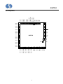
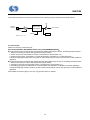
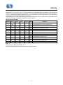
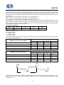
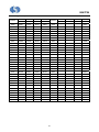
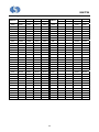
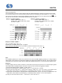
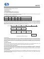
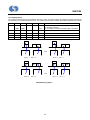
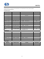
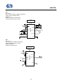
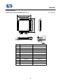
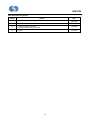
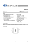
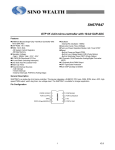
SH67P54 OTP 4-Bit Micro-controller with LCD Driver Features SH6610D-Based Single-Chip 4-Bit Micro-controller OTPROM: 4K X 16 bits RAM: 384 X 4bits - System Register: 48 X 4 bits - Data RAM: 336 X 4 bits Operation Voltage: System Oscillator = 300kHz - 4MHz, VDD = 2.4V - 6.0V System Oscillator = 30kHz - 8MHz, VDD = 4.5V - 6.0V 16 CMOS Bi-directional I/O Pins (PORT C, D can switch to segment) Built-in Pull-high and Pull-low Resistor for I/O 8-Level Subroutine Nesting (include interrupts) One 8-Bit Auto Re-load Timer/Counter Warm-Up Timer for Power-on Reset Powerful Interrupt Sources: - External Rising/Falling Interrupt - Timer0 Interrupt - Base Timer Interrupt - Port's Rising/Falling Edge Interrupt: PORTB, C 8-bit Base Timer LCD Driver: 8 X 30 (1/8 duty 1/4 bias), 6 X 32 (1/6 duty 1/3 bias), 5 X 33 (1/5 duty 1/3 bias), 4 X 34 dots (1/4 duty 1/3 bias) LCD used as Scan Output LCD shared as LED Matrix Built-in Dual Tone PSG with One Noise Generator Built-in Watchdog Timer Two LVR Level (Code Option) - Level1: 4.0V - Level2: 2.5V 2 Clock Sources OSC: (Code Option selects the type of OSC) - Crystal Oscillator: 32.768kHz - RC Oscillator: 262kHz OSCX: (system register selects the type of OSCX) - Ceramic Resonator/Crystal Oscillator: 400kHz - 8MHz - RC oscillator: 2MHz - 8MHz Instruction cycle time (4/fOSC): User program can read ROM data Two low power operation modes: HALT and STOP Low power consumption OTP type & Code protection Chip and LQFP64 General Description SH67P54 is a single chip micro-controller integrated with SRAM, 4K OTPROM, timer, watchdog timer and dual-tone PSG, LCD driver, LED Matrix driver and I/O port. 1 V2.2 SH67P54 NC NC COM1 COM2 COM3 COM4 COM5/SEG34 COM6/SEG33 COM7/SEG32 COM8/SEG31 SEG30 SEG29 SEG28 SEG27 SEG26 SEG25 LQFP64 PIN Configuration 48 47 46 45 44 43 42 41 40 39 38 37 36 35 34 33 SEG24 49 32 V1 SEG23 50 31 V2 SEG22 51 30 V3 SEG21 52 29 V4 SEG20 53 28 NC SEG19 54 27 RESET SEG18 55 26 TEST SEG17 56 25 OSCO SEG16 57 24 OSCI SEG15 58 23 OSCXO SEG14 59 22 OSCXI SEG13 60 21 VDD SEG12 61 20 GND SEG11 62 19 NC SEG10 63 18 PORTA.0 SEG9 64 17 PORTA.1 8 9 10 11 12 13 14 15 16 NC PORTD.3/SEG8 PORTD.2/SEG7 PORTD.1/SEG6 PORTD.0/SEG5 PORTC.3/SEG4 PORTC.2/SEG3 PORTC.1/SEG2 2 PORTA.2 7 PORTA.3 6 PORTB.0 5 PORTB.1 4 PORTB.2 3 PORTB.3 2 PORTC.0/SEG1 1 NC SH67P54 SH67P54 COM1 COM3 COM2 COM4 COM5/SEG34 COM7/SEG32 COM6/SEG33 SEG30 COM8/SEG31 SEG29 SEG28 SEG27 SEG25 SEG26 Pad Configuration 42 41 40 39 38 37 36 35 34 33 32 31 30 29 28 V1 44 27 V2 45 26 V3 SEG21 46 25 V4 SEG20 47 24 RESET SEG19 48 23 TEST SEG18 49 22 OSCO SEG17 50 21 OSCI SEG16 51 20 OSCXO SEG9 58 1 2 3 4 5 6 7 8 9 10 11 12 13 14 15 16 PORTA.0 57 PORTA.1 SEG10 PORTA.2 56 BD0 PORTA.3 SEG11 GND 17 PORTB.0 55 PORTB.1 SEG12 BD1 PORTB.2 54 PORTB.3 SEG13 VDD 18 PORTC.0/SEG1 53 PORTC.1/SEG2 SEG14 PORTC.2/SEG3 52 19 OSCXI PORTC.3/SEG4 SEG15 SH67P54 PORTD.0/SEG5 SEG22 PORTD.1/SEG6 SEG23 PORTD.2/SEG7 43 PORTD.3/SEG8 SEG24 3 SH67P54 Block Diagram ROM (4096 X 16) RAM (384 X 4) OSCS SH6610D 8-BIT TIMER0 CPU CORE PORTA & EXTERNAL INT I/O PORT SEGMENT LCD RESET RAM SCAN REGISTER PSG COMMON DRIVER GND CPU OPERATING VOLTAGE LCD VOLTAGE GENERATOR DRIVER V1 V2 V3 V4 4 OSCI OSCO OSCXI OSCXO PORTA.0 (INT0) PORTA.1 (PSG) PORTA.2 (PSG) PORTA.3 PORTB [3:0] PORTC [3:0] PORTD [3:0] SEG [30:9] (SEG[8:1] shared with PORTC &PORTD) COM [4:1] (COM[8:5] shared with SEG[31:34]) SH67P54 Pad Description Pad NO. Designation I/O Description 3, 4, 5, 6 PORTD [3:0] I/O Bit programmable I/O, shared with Segment 8 - 5 7, 8, 9, 10 PORTC [3:0] I/O Bit programmable I/O, shared with Segment 4 - 1 11, 12, 13, 14 PORTB [3:0] I/O Bit programmable I/O, Vector interrupt 15, 16, 17, 18 PORTA [3:0] I/O Bit programmable I/O, PORTA.1, PORTA.2 shared with PSG output 20 GND P Ground BD0 I Bonding option 0 VDD P Power supply BD1 I Bonding option 1 22 OSCXI I Oscillator X input 23 OSCXO O Oscillator X output 24 OSCI I Oscillator input 25 OSCO O Oscillator output 26 TEST I Test pin must be connected to GND 27 RESET I Reset input (No internal pull-high) 29, 30, 31, 32 V [4:1] I Connected with external LCD divided resistor 38, 37, 36, 35 COM [4:1] O Common signal output for LCD display 39, 40, 41, 42 COM5/SEG34, COM6/SEG33, COM7/SEG32, COM8/SEG31 O Common/segment signal output for LCD display 43 - 64 SEG [30:9] O Segment signal output for LCD display, Shared with scan output 21 Total: 58 Pads, 2 bonding Pads. OTP Programming Pin Description (OTP program mode) Pad NO. Designation I/O Shared by Description 21 VDD P VDD 27 VPP P RESET 20 GND P GND Ground 24 SCK I OSCI Programming Clock input pin 18 SDA I/O PORTA.0 Programming Power supply (+5.5V) Programming high voltage Power supply (+11.0V) Programming Data pin 5 SH67P54 Functional Description 1. CPU The CPU contains the following functional blocks: Program Counter (PC), Arithmetic Logic Unit (ALU), Carry Flag (CY), Accumulator, Table Branch Register, Data Pointer (INX, DPH, DPM, and DPL) and Stacks. 1.1. PC The PC is used for ROM addressing consisting of 12-bits: Page Register (PC11), and Ripple Carry Counter (PC10, PC9, PC8, PC7, PC6, PC5, PC4, PC3, PC2, PC1, PC0). The program counter is loaded with data corresponding to each instruction. The unconditional jump instruction (JMP) can be set at 1-bit page register for higher than 2K. The program counter cans only 4K program ROM address. (Refer to the ROM description). 1.2. ALU and CY The ALU performs arithmetic and logic operations. The ALU provides the following functions: Binary addition/subtraction (ADC, SBC, ADD, SUB, ADI, SBI) Decimal adjustments for addition/subtraction (DAA, DAS) Logic operations (AND, EOR, OR, ANDIM, EORIM, ORIM) Decisions (BA0, BA1, BA2, BA3, BAZ, BNZ, BC, BNC) Logic Shift (SHR) The Carry Flag (CY) holds the ALU overflow that the arithmetic operation generates. During an interrupt service or CALL instruction, the carry flag is pushed into the stack and recovered from the stack by the RTNI instruction. It is unaffected by the RTNW instruction. 1.3. Accumulator (AC) The accumulator is a 4-bit register holding the results of the arithmetic logic unit. In conjunction with the ALU, data is transferred between the accumulator and system register, or data memory can be performed. 1.4. Table Branch Register (TBR) Table Data can be stored in program memory and can be referenced by using Table Branch (TJMP) and Return Constant (RTNW) instructions. The TBR and AC are placed by an offset address in program ROM. TJMP instruction branch into address ((PC11 - PC8) X (28) + (TBR, AC)). The address is determined by RTNW to return look-up value into (TBR, AC). ROM code bit7-bit4 is placed into TBR and bit3-bit0 into AC. 1.5. Data Pointer The Data Pointer can indirectly address data memory. Pointer address is located in register DPH (3-bits), DPM (3-bits) and DPL (4-bits). The addressing range can have 3FFH locations. Pseudo index address (INX) is used to read or write Data memory, then RAM address bit9 - bit0 comes from DPH, DPM and DPL. 1.6. Stack The stack is a group of registers used to save the contents of CY & PC (11-0) sequentially with each subroutine call or interrupt. The MSB is saved for CY and it is organized into 13 bits X 8 levels. The stack is operated on a first-in, last-out basis and returned sequentially to the PC with the return instructions (RTNI/RTNW). Note: The stack nesting includes both subroutine calls and interrupts requests. The maximum allowed for subroutine calls and interrupts are 8 levels. If the number of calls and interrupt requests exceeds 8, then the bottom of stack will be shifted out, that program execution may enter an abnormal state. 2. OTPROM The ROM can address 4096 X 16 bits of program area from $000 to $FFF. 2.1. Vector Address Area ($000 to $004) The program is sequentially executed. There is an area address $000 through $004 that is reserved for a special interrupt service routine such as starting vector address. Address Instruction Remarks $000 JMP* Jump to RESET service routine $001 JMP* Jump to External interrupt service routine $002 JMP* Jump to Timer0 service routine $003 JMP* Jump to Base Timer service routine $004 JMP* Jump to PORT interrupt service routine *JMP instruction can be replaced by any instruction. 6 SH67P54 3. RAM Built-in RAM contains of general-purpose data memory and system register. Because of its static nature, the RAM can keep data after the CPU enters STOP or HALT. 3.1. RAM Addressing Data memory and system register can be accessed in one instruction by direct addressing. The following is the memory allocation map: System register and I/O: $000 - $01F, $370 - $377 Data memory: $020 - $16F LCD RAM space: $300 - $348 Segment scan output RAM: $358 - $36D 3.2. Configuration of System Register: System Register $00-$1F, $370 - $377 RAM Map: Address Bit3 Bit2 Bit1 Bit0 R/W Remarks $00 IEX IET0 IEBT IEP R/W Interrupt enable flags $01 IRQX IRQT0 IRQBT IRQP R/W Interrupt request flags $02 TM0.3 TM0.2 TM0.1 TM0.0 R/W Timer0 Mode register (Prescaler) $03 BTM.3 BTM.2 BTM.1 BTM.0 R/W Base timer mode register $04 TL0.3 TL0.2 TL0.1 TL0.0 R/W Timer0 load/counter register low nibble $05 TH0.3 TH0.2 TH0.1 TH0.0 R/W Timer0 load/counter register high nibble $06 - - - - - $07 - LCDON RLCD1 RLCD0 R/W Bit0, 1: Select LCD divider resistors Bit2: LCD on/off $08 PA.3 PA.2 PA.1 PA.0 R/W PORTA $09 PB.3 PB.2 PB.1 PB.0 R/W PORTB $0A PC.3 PC.2 PC.1 PC.0 R/W PORTC $0B PD.3 PD.2 PD.1 PD.0 R/W PORTD BD 1 BD 0 R $0C PAM2 PAM1 Reserved Bit0, 1: Bonding option. BD0 is weakly pulled high BD1 is weakly pulled low Bit2, 3: PORTA.1 & PORTA.2 as PSG output or I/O PORT R/W $0D LVD O/S2 O/S1 O/S0 R/W Bit0: Set PORTC as LCD segment Bit1: Set PORTD as LCD segment Bit2: Set segment as output port Bit3: LCD Voltage degrade $0E TBR.3 TBR.2 TBR.1 TBR.0 R/W Table Branch Register $0F INX.3 INX.2 INX.1 INX.0 R/W Pseudo index register $10 DPL.3 DPL.2 DPL.1 DPL.0 R/W Data pointer for INX low nibble $11 - DPM.2 DPM.1 DPM.0 R/W Data pointer for INX middle nibble $12 - DPH.2 DPH.1 DPH.0 R/W Data pointer for INX high nibble $13 PULLEN PH/PL PBCFR EINFR R/W Bit0: External interrupt (PORTA.0) rising/falling edge set Bit1: PORTB, PORTC interrupt rising/falling edge set Bit2: Port pull-high/low set Bit3: Port pull-high/low enable control $14 OXS - OXM OXON R/W Bit0: Turn on OSCX oscillator Bit1: CPU clocks select (1: OSCX/0: OSC) Bit3: OSCX type selection $15 LPS1 LPS0 DUTY0 DUTY1 R/W Bit0, 1: Select LCD DUTY (1/8, 1/6, 1/5 or 1/4) Bit2, 3: LCD frequency control 7 SH67P54 The Configuration of System Register (continue) Address Bit3 Bit2 Bit1 Bit0 R/W $16 PACR.3 PACR.2 PACR.1 PACR.0 R/W PORTA input/output control Remarks $17 PBCR.3 PBCR.2 PBCR.1 PBCR.0 R/W PORTB input/output control $18 PCCR.3 PCCR.2 PCCR.1 PCCR.0 R/W PORTC input/output control $19 PDCR.3 PDCR.2 PDCR.1 PDCR.0 R/W PORTD input/output control $1A RDT.3 RDT.2 RDT.1 RDT.0 R/W ROM Data table address/data register $1B RDT.7 RDT.6 RDT.5 RDT.4 R/W ROM Data table address/data register $1C RDT.11 RDT.10 RDT.9 RDT.8 R/W ROM Data table address/data register $1D RDT.15 RDT.14 RDT.13 RDT.12 R/W ROM Data table address/data register Bit0 - 2: Watchdog timer control Bit3: Watchdog timer overflow flag WDT.2 WDT.1 WDT.0 R/W R - - - - - $370 SEL1 SEL0 C2M C1M W Bit0, 1: PSG1, PSG2 mode control Bit2, 3: PSG1, PSG2 clock source selection $371 C1.3 C1.2 C1.1 C1.0 W PSG channel 1 low nibble $372 OCT1 C1.6 C1.5 C1.4 W PSG channel 1high nibble Bit3: channel 1 octave shift control $373 C2.3 C2.2 C2.1 C2.0 W PSG channel 2 nibble 1 or alarm output $1E WDF $1F Reserved $374 C2.7 C2.6 C2.5 C2.4 W PSG channel 2 nibble 2 $375 C2.11 C2.10 C2.9 C2.8 W PSG channel 2 nibble 3 $376 OCT2 C2.14 C2.13 C2.12 W PSG channel 2 nibble 4 Bit3: channel 2 octave shift control $377 VOL1 VOL0 CH2EN CH1EN W Bit0, Bit1: Channel 1, 2 enable Bit2, Bit3: volume control System Register $00 - $12. (Please refer to SH6610D User’s manual) 3.3. System Register Initial State: Address Bit 3 Bit 2 Bit 1 Bit 0 $00 IEX IET0 IEBT IEP Power On Reset /Pin Reset /Low Voltage Reset 0000 $01 IRQX IRQT0 IRQBT IRQP 0000 0000 WDT Reset 0000 $02 T0M.3 T0M.2 T0M.1 T0M.0 0000 uuuu $03 BTM.3 BTM.2 BTM.1 BTM.0 0000 uuuu $04 T0L.3 T0L.2 T0L.1 T0L.0 xxxx xxxx $05 T0H.3 T0H.2 T0H.1 T0H.0 xxxx xxxx $06 - - - - - - $07 - LCDON RLCD1 RLCD0 -000 -uuu $08 PA.3 PA.2 PA.1 PA.0 0000 0000 $09 PB.3 PB.2 PB.1 PB.0 0000 0000 8 SH67P54 System Register Initial State (continue): Address Bit 3 Bit 2 Bit 1 Bit 0 $0A PC.3 PC.2 PC.1 PC.0 Power On Reset /Pin Reset /Low Voltage Reset 0000 $0B PD.3 PD.2 PD.1 PD.0 0000 0000 $0C PAM2 PAM1 BD 1 BD 0 00xx uuxx $0D LVD O/S2 O/S1 O/S0 0000 uuuu $0E TBR.3 TBR.2 TBR.1 TBR.0 xxxx uuuu $0F INX.3 INX.2 INX.1 INX.0 xxxx uuuu $10 DPL.3 DPL.2 DPL.1 DPL.0 xxxx uuuu $11 - DPM.2 DPM.1 DPM.0 -xxx -uuu $12 - DPH.2 DPH.1 DPH.0 -xxx -uuu $13 PULLEN PH/PL PBCFR EINFR 0100 0uuu $14 OXS - OXM OXON 0-00 u-0u $15 LPS1 LPS0 DUTY1 DUTY0 0000 uuuu WDT Reset 0000 $16 PACR.3 PACR.2 PACR.1 PACR.0 0000 0000 $17 PBCR.3 PBCR.2 PBCR.1 PBCR.0 0000 0000 $18 PCCR.3 PCCR.2 PCCR.1 PCCR.0 0000 0000 $19 PDCR.3 PDCR.2 PDCR.1 PDCR.0 0000 0000 $1A RDT.3 RDT.2 RDT.1 RDT.0 0000 uuuu $1B RDT.7 RDT.6 RDT.5 RDT.4 0000 uuuu $1C RDT.11 RDT.10 RDT.9 RDT.8 0000 uuuu $1D RDT.15 RDT.14 RDT.13 RDT.12 0000 uuuu $1E WDF WDT.2 WDT.1 WDT.0 0000 1000 $1F - - - - - - $370 SEL1 SEL0 C2M C1M 0000 uuuu $371 C1.3 C1.2 C1.1 C1.0 0000 uuuu $372 OCT1 C1.6 C1.5 C1.4 0000 uuuu $373 C2.3 C2.2 C2.1 C2.0 0000 uuuu $374 C2.7 C2.6 C2.5 C2.4 0000 uuuu $375 C2.11 C2.10 C2.9 C2.8 0000 uuuu $376 OCT2 C2.14 C2.13 C2.12 0000 uuuu $377 VOL1 VOL0 CH2EN CH1EN 0000 uu00 Legend: x = unknown, u = unchanged, - = unimplemented read as '0'. 3.4. Others Initial State: Others After any Reset Program Counter (PC) $000 CY Undefined Accumulator (AC) Undefined Data Memory Undefined 9 SH67P54 4. System Clock and Oscillator 4.1. Circuit Configuration SH67P54 has two on-chip oscillation circuits OSC and OSCX. OSC is a low frequency crystal (Typ. 32.768kHz) or RC (Typ.262kHz) determined by the Code Option. This is designed for low frequency operation. OSCX also has two types: ceramic/crystal (Typ.455kHz) or RC (2MHz to 8MHz) to be determined by the software option. It is designed for high frequency operation. It is possible to select the high speed CPU processing by a high frequency clock and select low power operation by low operation clock. At the start of Power on reset, Pin reset and low power reset initialization, the OSC starts oscillation and OSCX is turned off. But at the start of WDT reset initialization, the OSC starts oscillation and OSCX remains the original state. Immediately after reset initialization, the OSC clock is automatically selected as the system clock input source. Oscillator Block Diagram OSCI Base Timer Low Frequency Clock Oscillator OSCO System clock Source Selector & Switching control OSCXI System clock Generator CPU Clock High Frequency OSCXO Clock Oscillator 4.2. OSC Oscillation The OSC generates the basic clock pulses that provide the CPU and peripherals (Base Timer, LCD) with an operating clock. OSC Crystal Oscillator Type 10P-15 P OSCI 32.768kHz Crystal CHIP OSCO 10P-15 P OSC RC Oscillator Type ROSC OSCI 102 CHIP OSCO 10 SH67P54 4.3. OSCX Oscillation OSCX has two clock oscillators. The software options select the Ceramic/Crystal or RC as the CPU's sub clock. If the OSCX is not used, it must be selected as a ceramic resonator and the OSCXI must be connected to GND. OSCX Ceramic/Crystal Oscillator Type 47P-100 P OSCXI 455kHz Ceramic CHIP OSCXO 47P-100 P OSCX RC Oscillator Type ROSCX OSCXI 102 CHIP OSCXO 4.4. Control of Oscillator The oscillator control register configuration is shown as follows: Address Bit3 Bit2 Bit1 Bit0 $14 OXS - OXM OXON OXON: OSCX oscillation on/off. 0: Turn-off OSCX oscillation 1: Turn-on OSCX oscillation OXM: switching system oscillator. 0: select OSC as system oscillator 1: select OSCX as system oscillator OXS: OSCX oscillator type selection 0: OSCX set as Ceramic Resonator/Crystal Oscillator 1: OSCX set as RC oscillator 4.5. Programming Notes It takes at least 5 ms for the OSCX oscillation circuit to turn on until the oscillation stabilizes. When switching the CPU system clock from OSC to OSCX, the user must wait a minimum of 5ms since the OSCX oscillation is running. However, the start time varies with respect to oscillator characteristics and the condition of use. Thus the wait time depends on the application. When switching from OSCX to OSC, the user should switch clock first then turn off OSCX. If switching from OSCX to OSC and turning off OSCX in one instruction, the OSCX turn off control will be delayed for one instruction cycle automatically to prevent CPU operation error. Following is the timing of system clock switching. OSCX turn off OSCX turn on OSCXO OSCO SYS CLOCK High frequency operation Low frequency operation High frequency operation Warm-up time Switch from OSCX to OSC Figure 1. Timing of System Clock Switching 11 Switch from OSCX to OSC SH67P54 4.6. System Clock The system clock varies as the clock source changes. The following table shows the instruction execution time according to each frequency of the system clock source. OSCFREQ 32.768kHz (OSC) 262kHz (OSC) 455kHz (OSCX) 2MHz (OSCX) 8MHz (OSCX) Cycle time 122.07 µs 15.27 µs 8.79 µs 2 µs 0.5 µs 5. Low Voltage Reset (LVR) The LVR function is to monitor the supply voltage and generate an internal reset in the device. It is typically used in AC line applications or large battery where large loads may be switched in and cause the device voltage to temporarily fall below the specified operating minimum. 5.1. Functions of the LVR Circuit The LVR function is selected by Code Option. The LVR circuit has the following functions: - It generates an internal reset signal when VDD ≤ VLVR - It cancels the internal reset signal when VDD > VLVR Here, VDD: power supply voltage, VLVR: LVR detect voltage, there are two level selected by Code Option: Level1: 2.4 - 2.6V, typical 2.5V Level2: 3.8 - 4.2V, typical 4.0V 12 SH67P54 6. I/O Ports The MCU provides 16 bi-directional I/O pins. Each I/O pin contains pull high/low MOS controllable through programming. When every I/O is used as input, the PORT control register (PACR, PBCR, PCCR, PDCR) controls the ON/OFF of the output buffer. Every I/O pin has an internal pull high/low resistor, which is controlled by PULLEN, PH/PL of $13 and data of the port. Port I/O mapping address is shown as follows: Address Bit3 Bit2 Bit1 Bit0 R/W Remarks $08 PA.3 PA.2 PA.1 PA.0 R/W PORTA $09 PB.3 PB.2 PB.1 PB.0 R/W PORTB $0A PC.3 PC.2 PC.1 PC.0 R/W PORTC $0B PD.3 PD.2 PD.1 PD.0 R/W PORTD $16 PACR.3 PACR.2 PACR.1 PACR.0 R/W PORTA input/output control $17 PBCR.3 PBCR.2 PBCR.1 PBCR.0 R/W PORTB input/output control $18 PCCR.3 PCCR.2 PCCR.1 PCCR.0 R/W PORTC input/output control $19 PDCR.3 PDCR.2 PDCR.1 PDCR.0 R/W PORTD input/output control Equivalent Circuit for a Single I/O Pin VDD PULLEN PH/PL VDD Weak Pull high I/O Control Register I/O Pad DATA Regiser GND GND READ DATA IN DATA Weak Pull Low READ System Register $13 Address $13 Bit3 PULLEN Bit2 PH/PL Bit1 PBCFR Bit0 EINFR Remarks R/W Bit0: External interrupt (PORTA.0) rising/falling edge set Bit1: PORTB, PORTC interrupt rising/failing edge set R/W Bit2: Port pull-high/low set Bit3: Port pull-high/low enable control EINFR: 1: External Rising Edge interrupt 0: External Falling Edge interrupt PBCFR: 1: PORTB, PORTC Rising Edge interrupt 0: PORTB, PORTC Falling Edge interrupt PH/PL: 1: Port Pull high resistor ON 0: Port Pull low resistor ON PULLEN: 1: Port Pull high/low enable 0: Port Pull high/low disable To turn on the pull high resistor, user must set PULLEN to 1, set PH/PL to 1, and write 1 to the port data register. To turn on the pull low resistor, user must set PULLEN to 1, set PH/PL to 0, and write 0 to the port data register. 13 SH67P54 6.1. PORTB & PORTC Interrupt The PORTB and PORTC are used as port interrupt sources. Following is the port interrupt function block-diagram. IEP PORTB.n PORTC.n Rising / Falling Edge Detector Port Interrupt PBCR.n PCCR.n IRQP PBCFR Note: n = 0, 1, 2, 3 6.2. External INT0 PORTA.0 is shared by external interrupts. External INT0 (PORTA.0) AND PORTB, PORTC interrupt PROGRAMMING NOTES: If user wants to generate an interrupt when a rising edge from GND to VDD emerges in the port, the following must be executed. 1. Set the port as input port, fill port data register and avoid port floating. 2. Pull low the port (Use external pull low resistor or set PULLEN to 1and set PH/PL to 0). 3. Set Rising Edge register. (Set PBCFR to 1 in PBC INT application. Set EINFR to 1 in EXINT application.) And further rising edge transition would not be able to make interrupt request until all of the pins return to GND in PBC INT application. If user wants to generate an interrupt when a falling edge from VDD to GND emerges on the port, the following must be executed. 1. Set the port as input port, fill port data register and avoid port floating. 2. Pull high the port (Use external pull high resistor or set PULLEN to 1and set PH/PL to 1). 3. Set Falling Edge register. (Set PBCFR to 0 in PORTB, PORTC INT application. Set EINFR to 0 in EXINT application). And further falling edge transition would not be able to make interrupt request until all of the pins return to VDD in PBC INT application. When PORTC is shared to segment, user can only generate interrupt on PORTB. 14 SH67P54 7. Timer 0 SH67P54 has one 8-bit timer. The timer consists of an 8-bit up counter and an 8-bit preload register. The timers provide the following functions: - Programmable internal timer function - Read the counter values 7.1. Timer 0 Configuration and Operation The timer 0 consists of an 8-bit write-only timer load register (TL0L, TL0H) and an 8-bit read-only timer counter (TC0L, TC0H). Each has low order digits and high order digits. The timer counter can be initialized by writing data into the timer load register (TL0L, TL0H). Write the low-order digit first and then the high-order digit. The timer counter is loaded with the content of the load register automatically when the high order digit is written or counts overflow happens. The timer overflow will generate an interrupt, if the interrupt enable flag is set. The timer can be programmed in several different system clock sources by setting the Timer Mode register (TM0). Timer 0 reads and writes operations follow these rules: Write Operation Read Operation Low nibble first High nibble first High nibble to update the counter Low nibble follows 7.2. Timer0 Mode Register (TM0) The 8-bit counter counts prescaler overflow output pulses. TM0 are 4-bit registers used for timer control as shown in Table 1. The register selects the input clock sources in the timer. Table 1. Timer0 Mode Registers ($02) TM0.3 TM0.2 TM0.1 TM0.0 Prescaler Clock Source - 0 0 0 /2048 System clock - 0 0 1 /512 System clock - 0 1 0 /128 System clock - 0 1 1 /32 System clock - 1 0 0 /8 System clock - 1 0 1 /4 System clock - 1 1 0 /2 System clock - 1 1 1 /1 PORTA.0(Falling Edge) TM0.3 control function: 0: without Auto-Reload function 1: Auto-Reload function 15 SH67P54 8. Base Timer The MCU has a base timer which the clock source is OSC (Low frequency oscillation: Crystal 32.768kHz or RC 262kHz). After MCU is reset, it counts at every clock-input signal. When it counts to $FF, right after next clock input, counter counts to $00 and generates an overflow. This causes the interrupt of base timer interrupt request flag to 1. Therefore, the base timer can function as an interval timer periodically, generating overflow output as every 256th clock signal output. The timer accepts 4096Hz or 32.75kHz clock, and base timer generates an accurate timing interrupt. This clock-input source is selected by BTM register. Address Bit3 Bit2 Bit1 Bit0 $03 BTM.3 BTM.2 BTM.1 BTM.0 1 0 X X Enable the base timer X X Disable the base timer, clear base timer counters and keep them as $00 Else states Remarks Base timer mode register BTM.1 BTM.0 Prescaler Ratio Clock Source 0 0 /1 4096Hz or 32.75kHz 0 1 /4 4096Hz or 32.75kHz 1 0 /8 4096Hz or 32.75kHz 1 1 /16 4096Hz or 32.75kHz MPX 32.768kHz or 262kHz /8 4096Hz or 32.75kHz /4 /8 /16 BTM [3:2] /1 8 Bit base timer counter 4Bit Scaler 16 SH67P54 9. Watchdog Timer (WDT) Watchdog timer is a down-count counter, and its clock source is an independent built-in RC oscillator, so that the WDT will always run even in the STOP mode (if it is enabled). The watchdog timer automatically generates a device reset when it overflows. Code Option can enable or disable this function. The watchdog timer control register (WDT bit2 - 0) selects different overflow frequency. WDT bit3 is watchdog timer overflow flag. If the Watchdog timer is enabled, the CPU will be reset when watchdog timer overflows. Repeat reads or writes WDT register ($1E), the watchdog timer should re-count before the overflow happens. System Register $1E: (WDT) Address $1E Bit 3 Bit 2 Bit 1 Bit 0 R/W WDT.2 WDT.1 WDT.0 R/W R Bit2 - 0: Watchdog timer control Bit3: Watchdog timer overflow flag (Read only) X 0 0 0 R/W Watchdog timer-out period = 4096ms X 0 0 1 R/W Watchdog timer-out period = 1024ms X 0 1 0 R/W Watchdog timer-out period = 256ms X 0 1 1 R/W Watchdog timer-out period = 128ms X 1 0 0 R/W Watchdog timer-out period = 64ms X 1 0 1 R/W Watchdog timer-out period = 16ms X 1 1 0 R/W Watchdog timer-out period = 4ms X 1 1 1 R/W Watchdog timer-out period = 1ms 0 X X X R No watchdog timer overflow reset 1 X X X R Watchdog timer overflow, WDT reset happens WDF Remarks Note: Watchdog timer-out period valid for VDD = 5V. WDF will be cleared after Power on Reset, Pin Reset or Low Power Reset. 17 SH67P54 10. LCD Driver The LCD driver contains a controller, a voltage generator, 8 common signal pins and 30 segment driver pins when LCD dots are maximum. There are four different programmable driving modes: 1/8 duty & 1/4 bias, 1/6 duty & 1/3 bias, 1/5 duty & 1/3 bias and 1/4 bias & 1/3bias. The driving modes are controlled by the system register $15 and the power-on initialization status is 1/8 duty, 1/4 bias. When 1/6 duty and 1/3 bias mode are used, COM7 - 8 are used as SEG32 - 31. When 1/5 duty and 1/3 bias mode are used, COM6 - 8 are used as SEG33 - 31. When 1/4 duty and 1/3 bias mode are used, COM5 - 8 are used as SEG34 - 31. The LCD SEG9 - 30 can also be used as output port controlled by the bit 2 of the system register $0D. When SEG9 - 30 are used as output ports, data must be written to bit 0 of the same addresses ($358 - $36D). LCD RAM could be used as data memory if necessary. When the "STOP" instruction is executed, the LCD will be turned off, but the data of LCD RAMs keep the same value before executing the "STOP" instruction. 10.1. LCD Control Register Address Bit 3 Bit 2 Bit 1 Bit 0 $15 LPS1 LPS0 DUTY1 DUTY0 DUTY1, 0: LCD duty control 0, 0: 1/8 duty, 1/4 bias 0, 1: 1/6 duty, 1/3 bias 1, 0: 1/5 duty, 1/3 bias 1, 1: 1/4 duty, 1/3 bias LPS1, LPS0: LCD frame frequency control. LCD clock is divided from OSC, so LCD frame frequency will change in proportion to the variation of OSC frequency. LPS1, LPS0 FRAME Frequency (OSC = 32.768kHz) 0, 0 0, 1 1, 0 1, 1 IN 1/8 DUTY MODE 32Hz 16Hz 8Hz 4Hz IN 1/6 DUTY MODE 34.1Hz 17.0Hz 8.5Hz 4.2Hz IN 1/5 DUTY MODE 34.1Hz 17.0Hz 8.5Hz 4.2Hz IN 1/4 DUTY MODE 32Hz 16Hz 8Hz 4Hz LPS1, LPS0 FRAME Frequency (OSC = 262kHz) 0, 0 0, 1 1, 0 1, 1 IN 1/8 DUTY MODE 256Hz 128Hz 64Hz 32Hz IN 1/6 DUTY MODE 273Hz 136Hz 68Hz 34Hz IN 1/5 DUTY MODE 273Hz 136Hz 68Hz 34Hz IN 1/4 DUTY MODE 256Hz 128Hz 64Hz 32Hz COM1 COM1 ONE FRAME When the CPU is in STOP mode, the COMx and SEGx are pulled low. It can easily be woken up by a keyboard scan (Port interrupt). When the CPU is in HALT mode, the COMx and SEGx are normal. It can easily be woken up by base timer﹑timer0 or port interrupt. 18 SH67P54 10.2. LCD Power VDD Power Switch LCDON Power Degrade LVD LCD COM1 common driver COM8 LCD Power Supply Control Circuit LCD SEG1 segment driver OSC Pre-scaler LPS0 LPS1 LCDCLK DUTY0 DUTY1 Duty Control & scan output SEG34 Built-in special LCD power control for LCD power modulation. Address Bit 3 Bit 2 Bit 1 Bit 0 $0D LVD O/S2 O/S1 O/S0 O/S2: Set LCD SEG9-SEG30 to be LCD segment output or scan output ports 0: LCD segment output 1: scan output ports. O/S1: Set PORTD as LCD segment or I/O PORT 0: I/O PORT 1: LCD segments. O/S0: Set PORTC as LCD segment or I/O PORT 0: I/O PORT 1: LCD segments. When LVD is set to 1 and the divider resistors is 270kΩ, the LCD voltage power will be degraded to about 90% of VDD. It is designed to reduce extra LCD contrast control output pins. Then the LCD can be fitted automatically for different voltage levels by the software. 10.3. LCD on/off Control and Divider Resistors Setting Address Bit 3 Bit 2 Bit 1 Bit 0 $07 - LCDON RLCD1 RLCD0 VDD LCDON: LCD on/off switch. 0: LCD off. 1: LCD on. * When LCD is off, COM & SEG output GND in LCD application. If LCD is off and LCD is shared to LED application, COM output VDD and SEG output GND. LCDON LVD Power Switch Power Degrade V2 LCD RLCD1, RLCD0: LCD divider resistors setting 0, 0: R1 = R2 = R3 = R4 = 270kΩ (Default) 0, 1: R1 = R2 = R3 = R4 = 90kΩ 1, 0: R1 = R2 = R3 = R4 = 30kΩ 1, 1: R1 = R2 = R3 = R4 = 10kΩ When large LCD panel is used, user can set the value of $07 to increase the bias current for better LCD performance. But it will cost more power, when smaller divider resistors are used. User can also use external parallel connection resistors for complex bias current. Power Supply Control Circuit V1 R1 R2 R3 V3 R4 SH67P54 19 V4 SH67P54 10.4. Configuration of LCD RAM LCD 1/4 Duty, 1/3 Bias (COM1 - 4, SEG1 - 34) Address Bit3 Bit2 Bit1 Bit0 Address Bit3 Bit2 Bit1 Bit0 COM4 COM3 COM2 COM1 COM4 COM3 COM2 COM1 $300 SEG1 SEG1 SEG1 SEG1 $311 SEG18 SEG18 SEG18 SEG18 $301 SEG2 SEG2 SEG2 SEG2 $312 SEG19 SEG19 SEG19 SEG19 $302 SEG3 SEG3 SEG3 SEG3 $313 SEG20 SEG20 SEG20 SEG20 $303 SEG4 SEG4 SEG4 SEG4 $314 SEG21 SEG21 SEG21 SEG21 $304 SEG5 SEG5 SEG5 SEG5 $315 SEG22 SEG22 SEG22 SEG22 $305 SEG6 SEG6 SEG6 SEG6 $316 SEG23 SEG23 SEG23 SEG23 $306 SEG7 SEG7 SEG7 SEG7 $317 SEG24 SEG24 SEG24 SEG24 $307 SEG8 SEG8 SEG8 SEG8 $318 SEG25 SEG25 SEG25 SEG25 $308 SEG9 SEG9 SEG9 SEG9 $319 SEG26 SEG26 SEG26 SEG26 $309 SEG10 SEG10 SEG10 SEG10 $31A SEG27 SEG27 SEG27 SEG27 $30A SEG11 SEG11 SEG11 SEG11 $31B SEG28 SEG28 SEG28 SEG28 $30B SEG12 SEG12 SEG12 SEG12 $31C SEG29 SEG29 SEG29 SEG29 $30C SEG13 SEG13 SEG13 SEG13 $31D SEG30 SEG30 SEG30 SEG30 $30D SEG14 SEG14 SEG14 SEG14 $31E SEG31 SEG31 SEG31 SEG31 $30E SEG15 SEG15 SEG15 SEG15 $31F SEG32 SEG32 SEG32 SEG32 $30F SEG16 SEG16 SEG16 SEG16 $320 SEG33 SEG33 SEG33 SEG33 $310 SEG17 SEG17 SEG17 SEG17 $321 SEG34 SEG34 SEG34 SEG34 20 SH67P54 LCD 1/5 Duty, 1/3 Bias (COM1 - 5, SEG1 - 33) Bit3 Bit2 Bit1 Bit0 COM4 COM3 COM2 COM1 $300 SEG1 SEG1 SEG1 SEG1 $301 SEG2 SEG2 SEG2 $302 SEG3 SEG3 $303 SEG4 SEG4 $304 SEG5 $305 SEG6 $306 $307 Address Bit3 Bit2 Bit1 Bit0 - - - COM5 $328 - - - SEG1 SEG2 $329 - - - SEG2 SEG3 SEG3 $32A - - - SEG3 SEG4 SEG4 $32B - - - SEG4 SEG5 SEG5 SEG5 $32C - - - SEG5 SEG6 SEG6 SEG6 $32D - - - SEG6 SEG7 SEG7 SEG7 SEG7 $32E - - - SEG7 SEG8 SEG8 SEG8 SEG8 $32F - - - SEG8 Address $308 SEG9 SEG9 SEG9 SEG9 $330 - - - SEG9 $309 SEG10 SEG10 SEG10 SEG10 $331 - - - SEG10 $30A SEG11 SEG11 SEG11 SEG11 $332 - - - SEG11 $30B SEG12 SEG12 SEG12 SEG12 $333 - - - SEG12 $30C SEG13 SEG13 SEG13 SEG13 $334 - - - SEG13 $30D SEG14 SEG14 SEG14 SEG14 $335 - - - SEG14 $30E SEG15 SEG15 SEG15 SEG15 $336 - - - SEG15 $30F SEG16 SEG16 SEG16 SEG16 $337 - - - SEG16 $310 SEG17 SEG17 SEG17 SEG17 $338 - - - SEG17 $311 SEG18 SEG18 SEG18 SEG18 $339 - - - SEG18 $312 SEG19 SEG19 SEG19 SEG19 $33A - - - SEG19 $313 SEG20 SEG20 SEG20 SEG20 $33B - - - SEG20 $314 SEG21 SEG21 SEG21 SEG21 $33C - - - SEG21 $315 SEG22 SEG22 SEG22 SEG22 $33D - - - SEG22 $316 SEG23 SEG23 SEG23 SEG23 $33E - - - SEG23 $317 SEG24 SEG24 SEG24 SEG24 $33F - - - SEG24 $318 SEG25 SEG25 SEG25 SEG25 $340 - - - SEG25 $319 SEG26 SEG26 SEG26 SEG26 $341 - - - SEG26 $31A SEG27 SEG27 SEG27 SEG27 $342 - - - SEG27 $31B SEG28 SEG28 SEG28 SEG28 $343 - - - SEG28 $31C SEG29 SEG29 SEG29 SEG29 $344 - - - SEG29 $31D SEG30 SEG30 SEG30 SEG30 $345 - - - SEG30 $31E SEG31 SEG31 SEG31 SEG31 $346 - - - SEG31 $31F SEG32 SEG32 SEG32 SEG32 $347 - - - SEG32 $320 SEG33 SEG33 SEG33 SEG33 $348 - - - SEG33 21 SH67P54 LCD 1/6 Duty, 1/3 Bias (COM1 - 6, SEG1 - 32) Bit3 Bit2 Bit1 Bit0 COM4 COM3 COM2 COM1 $300 SEG1 SEG1 SEG1 SEG1 $301 SEG2 SEG2 SEG2 $302 SEG3 SEG3 $303 SEG4 SEG4 $304 SEG5 $305 SEG6 $306 $307 Address Bit3 Bit2 Bit1 Bit0 - - COM6 COM5 $328 - - SEG1 SEG1 SEG2 $329 - SEG2 SEG2 SEG3 SEG3 $32A - SEG3 SEG3 SEG4 SEG4 $32B - SEG4 SEG4 SEG5 SEG5 SEG5 $32C - - SEG5 SEG5 SEG6 SEG6 SEG6 $32D - - SEG6 SEG6 SEG7 SEG7 SEG7 SEG7 $32E - - SEG7 SEG7 SEG8 SEG8 SEG8 SEG8 $32F - - SEG8 SEG8 Address $308 SEG9 SEG9 SEG9 SEG9 $330 - - SEG9 SEG9 $309 SEG10 SEG10 SEG10 SEG10 $331 - - SEG10 SEG10 $30A SEG11 SEG11 SEG11 SEG11 $332 - - SEG11 SEG11 $30B SEG12 SEG12 SEG12 SEG12 $333 - - SEG12 SEG12 $30C SEG13 SEG13 SEG13 SEG13 $334 - - SEG13 SEG13 $30D SEG14 SEG14 SEG14 SEG14 $335 - - SEG14 SEG14 $30E SEG15 SEG15 SEG15 SEG15 $336 - - SEG15 SEG15 $30F SEG16 SEG16 SEG16 SEG16 $337 - - SEG16 SEG16 $310 SEG17 SEG17 SEG17 SEG17 $338 - - SEG17 SEG17 $311 SEG18 SEG18 SEG18 SEG18 $339 - - SEG18 SEG18 $312 SEG19 SEG19 SEG19 SEG19 $33A - - SEG19 SEG19 $313 SEG20 SEG20 SEG20 SEG20 $33B - - SEG20 SEG20 $314 SEG21 SEG21 SEG21 SEG21 $33C - - SEG21 SEG21 $315 SEG22 SEG22 SEG22 SEG22 $33D - - SEG22 SEG22 $316 SEG23 SEG23 SEG23 SEG23 $33E - - SEG23 SEG23 $317 SEG24 SEG24 SEG24 SEG24 $33F - - SEG24 SEG24 $318 SEG25 SEG25 SEG25 SEG25 $340 - - SEG25 SEG25 $319 SEG26 SEG26 SEG26 SEG26 $341 - - SEG26 SEG26 $31A SEG27 SEG27 SEG27 SEG27 $342 - - SEG27 SEG27 $31B SEG28 SEG28 SEG28 SEG28 $343 - - SEG28 SEG28 $31C SEG29 SEG29 SEG29 SEG29 $344 - - SEG29 SEG29 $31D SEG30 SEG30 SEG30 SEG30 $345 - - SEG30 SEG30 $31E SEG31 SEG31 SEG31 SEG31 $346 - - SEG31 SEG31 $31F SEG32 SEG32 SEG32 SEG32 $347 - - SEG32 SEG32 22 SH67P54 LCD 1/8 Duty, 1/4 Bias (COM1 - 8, SEG1 - 30) Bit3 Bit2 Bit1 Bit0 COM4 COM3 COM2 COM1 $300 SEG1 SEG1 SEG1 SEG1 $301 SEG2 SEG2 SEG2 $302 SEG3 SEG3 $303 SEG4 SEG4 $304 SEG5 $305 SEG6 $306 $307 Address Bit3 Bit2 Bit1 Bit0 COM8 COM7 COM6 COM5 $328 SEG1 SEG1 SEG1 SEG1 SEG2 $329 SEG2 SEG2 SEG2 SEG2 SEG3 SEG3 $32A SEG3 SEG3 SEG3 SEG3 SEG4 SEG4 $32B SEG4 SEG4 SEG4 SEG4 SEG5 SEG5 SEG5 $32C SEG5 SEG5 SEG5 SEG5 SEG6 SEG6 SEG6 $32D SEG6 SEG6 SEG6 SEG6 SEG7 SEG7 SEG7 SEG7 $32E SEG7 SEG7 SEG7 SEG7 SEG8 SEG8 SEG8 SEG8 $32F SEG8 SEG8 SEG8 SEG8 Address $308 SEG9 SEG9 SEG9 SEG9 $330 SEG9 SEG9 SEG9 SEG9 $309 SEG10 SEG10 SEG10 SEG10 $331 SEG10 SEG10 SEG10 SEG10 $30A SEG11 SEG11 SEG11 SEG11 $332 SEG11 SEG11 SEG11 SEG11 $30B SEG12 SEG12 SEG12 SEG12 $333 SEG12 SEG12 SEG12 SEG12 $30C SEG13 SEG13 SEG13 SEG13 $334 SEG13 SEG13 SEG13 SEG13 $30D SEG14 SEG14 SEG14 SEG14 $335 SEG14 SEG14 SEG14 SEG14 $30E SEG15 SEG15 SEG15 SEG15 $336 SEG15 SEG15 SEG15 SEG15 $30F SEG16 SEG16 SEG16 SEG16 $337 SEG16 SEG16 SEG16 SEG16 $310 SEG17 SEG17 SEG17 SEG17 $338 SEG17 SEG17 SEG17 SEG17 $311 SEG18 SEG18 SEG18 SEG18 $339 SEG18 SEG18 SEG18 SEG18 $312 SEG19 SEG19 SEG19 SEG19 $33A SEG19 SEG19 SEG19 SEG19 $313 SEG20 SEG20 SEG20 SEG20 $33B SEG20 SEG20 SEG20 SEG20 $314 SEG21 SEG21 SEG21 SEG21 $33C SEG21 SEG21 SEG21 SEG21 $315 SEG22 SEG22 SEG22 SEG22 $33D SEG22 SEG22 SEG22 SEG22 $316 SEG23 SEG23 SEG23 SEG23 $33E SEG23 SEG23 SEG23 SEG23 $317 SEG24 SEG24 SEG24 SEG24 $33F SEG24 SEG24 SEG24 SEG24 $318 SEG25 SEG25 SEG25 SEG25 $340 SEG25 SEG25 SEG25 SEG25 $319 SEG26 SEG26 SEG26 SEG26 $341 SEG26 SEG26 SEG26 SEG26 $31A SEG27 SEG27 SEG27 SEG27 $342 SEG27 SEG27 SEG27 SEG27 $31B SEG28 SEG28 SEG28 SEG28 $343 SEG28 SEG28 SEG28 SEG28 $31C SEG29 SEG29 SEG29 SEG29 $344 SEG29 SEG29 SEG29 SEG29 $31D SEG30 SEG30 SEG30 SEG30 $345 SEG30 SEG30 SEG30 SEG30 SEG9 - 30 is used as scan output port Address Bit0 Address Bit0 Address Bit0 Address Bit0 $358 SEG9 $35E SEG15 $364 SEG21 $36A SEG27 $359 SEG10 $35F SEG16 $365 SEG22 $36B SEG28 $35A SEG11 $360 SEG17 $366 SEG23 $36C SEG29 $35B SEG12 $361 SEG18 $367 SEG24 $36D SEG30 $35C SEG13 $362 SEG19 $368 SEG25 $35D SEG14 $363 SEG20 $369 SEG26 23 SH67P54 10.5. LCD Waveform 1/8 DUTY 1/4 BIAS SELECT UNSELECT 1/4 DUTY 1/3 BIAS SELECT UNSELECT V1 V2 V2 COM V3 COM V1 V3 GND V4 GND UNSELECT SELECT V1 SELECT V2 SEG SEG V3 GND GND Example the output waveform of 1/8 duty and 1/4 bias V1 V2 V3 V4 GND V1 V2 COM2 V3 V4 GND V1 V2 COM3 V3 V4 GND VDD V1 SEG V1 V2 V3 V4 COM1 UNSELECT V2 V3 GND 24 SH67P54 Example 1/4 Duty 1/3 Bias COM4 V3 V2 COM1 COM3 V1 0 V3 COM2 V2 COM2 V1 COM1 0 V3 V2 COM3 V1 0 V3 V2 COM4 V1 0 SEGn+1 V3 SEGn V2 SEGn V1 0 V V2 SEGn+1 V1 0 V3 V V1 COM4 - SEGn 0 -V1 -V2 -V3 10.6. Shared to LED Application User can use SEG & COM in the application of LED matrix by Code Option and configuration of LED RAM is the same as LCD RAM. Application Note The SEG & COM can not driver the LED matrix directly for the cause of weak driving ability. So in the LED Matrix application the driving circuit will be used such as following. Example 1/8 Duty LED Matrix Application Circuit. VDD VDD VDD COM1 COM2 COM3 COM1' SEG1' SEG2' SEG1 GND GND SEG30' SEG29 GND COM3' LED Matrix 8X30 dots SEG29' SEG2 COM2' SEG30 GND 25 VDD COM8 COM8' SH67P54 10.7. LED Waveform 1/8 DUTY UNSELECT 1/4 DUTY UNSELECT VDD COM VDD COM SELECT SELECT GND SELECT SELECT SELECT SELECT VDD SEG GND SELECT SELECT VDD SEG UNSELECT UNSELECT GND UNSELECT UNSELECT GND Example 1/4 Duty 4X10 Dots VDD GND COM1 COM2 COM1' COM3 COM2' COM4 COM3' SEG1 GND COM4' SEG2 SEG3 SEG1' SEG2' SEG3' SEG4'SEG5' SEG6' SEG7' SEG8' SEG9' SEG10' SEG4 SEG5 COMx' & SEGx'refer to the driving-amplified output of COMx & SEGx. SEG6 GND VDD SEG7 SEG8 SEG9 SEG10 GND 11. Read ROM DATA Address Bit 3 Bit 2 Bit 1 Bit 0 R/W Remarks $1A RDT.3 RDT.2 RDT.1 RDT.0 R/W ROM Data table address/data register $1B RDT.7 RDT.6 RDT.5 RDT.4 R/W ROM Data table address/data register $1C RDT.11 RDT.10 RDT.9 RDT.8 R/W ROM Data table address/data register $1D RDT.15 RDT.14 RDT.13 RDT.12 R/W ROM Data table address/data register The RDT register consists of a 12-bit write-only PC address load register (RDT.11 - RDT.0) and a 16-bit read-only ROM table data read-out register (RDT.15 - RDT.0). To read out the ROM table data, users should write the ROM table address to RDT register first (high nibble first then low nibble), then after one instruction, the right data will put into RDT register automatically (write lowest nibble of address into $1A will start the data read-out action). 26 SH67P54 12. Programmable Sound Generator (PSG) PSG has channel1 and channel2. The function block diagram is shown as follows: CHANNEL1 CH1 CLK OSC MIXER MPX OSCX CHANNEL2 CH2 CLK PSG PSG The PSG function provides four sub functions for wide applications. Programmable Sound Two channels create programmable sound. Every channel can be programmed as follows: - Enable/Disable every channel sounds. - Select every channel sound frequency. - Two channel sounds are mixed into one PSG output. - The PSG output can be controlled at 4 volume levels. Fine Noise PSG can provide wide-band noise. The wide-band noise volume can be controlled at 4 volume levels. Alarm PSG can provide many alarm functions by the software. The alarm carrier frequency can be programmed individually. The alarm volume can be controlled at 4 volume levels. Remote Control The remote control is the only expandable application for PSG sound. Since the remote control frequency is 56.13kHz or 37.92kHz, the software can select the sound frequency. 12.1. PSG Sub Block Diagram MPX block diagram SEL0 OSC SEL1 /2 CLOCK-SLECTOR OSCX PSG CLocK /16 SEL1 SEL0 Clock Source OSC clock PSG clock 0 0 OSC OSC = 32.768kHz 32.768kHz OSC = 262kHz 262kHz 0 1 OSC/2 OSC = 32.768kHz 16.384kHz OSC = 262kHz 131kHz OSCX = 1.8MHz 1.8MHz OSCX = 455kHz 455kHz OSCX = 1.8MHz 112.5kHz OSCX = 455kHz 28.4kHz 1 1 0 1 OSCX OSCX/16 The MPX block selects 4 clock sources as PSG clock that provides the two channel clock sources. 27 SH67P54 Channel 1 CH1EN OCT1 REGISTER C1.6 ~ C1.0 /8 PSG CLOCK SELECTOR OCT1 Scaling ratio 0 1 1 1/8 DIVIDER 1 /2 CH1 OUT Channel 1 is constructed by a 7-bit pseudo random counter. Channel 1 is enabled/disabled by CH1EN. It creates either a sound frequency or an alarm carrier frequency or a remote carrier frequency Channel 2 C2M NOISE GENERATOR CH2EN OCT2 PSG SELECTOR C2.14 ~ C2.0 /8 CLK CH2 OUT REGISTER C2.14 ~ C2.0 SELECTOR C2.14 ~ C2.8 DIVIDER 2 C2.3 ~ C2.0 /2 C1M 1Hz 4Hz ENEVLOP ENEVLOP 8Hz 32Hz OCT2 Scaling ratio 0 1 1 1/8 C2M A 15-bit pseudo random counter, construct channel 2. Channel 2 is enabled/disabled by CH2EN It can be a 15-bit wide-band noise generator or a 7-bit sound generator. It can also create an alarm envelope signal. C1M Remarks 0 0 CH1 is a Sound generator. CH2 is a Sound generator. 1 0 CH1 is a Sound generator. CH2 is a Noise generator. x 1 CH1 is a Sound generator. CH2 is an Alarm mode register. 28 SH67P54 Mixer TIME SLOT VOL0 VOL1 PAM1 PA.1 I/O PSG CH1 OUT TIME SLOT CH2 OUT SELECTOR1 PORTA.1 SELECTOR2 PORTA.2 VOL CONTROL PSG PA.2 I/O PAM2 The MIXER mixes CH1-OUT and CH2-OUT into one tone output to PORTA.1、PORTA.2, when PAM1 = 1、PAM2 = 1. Then the tone output is controlled by the volume control bit into 4 volume levels and in the end outputted by PSG. PORTA.1 & PORTA.2 are controlled by PAM1 & PAM2 PAM2 PAM1 Remarks 0 0 PORTA.1: I/O PORT PORTA.2: I/O PORT 0 1 PORTA.1: PSG output PORTA.2: I/O PORT 1 0 PORTA.1: I/O PORT PORTA.2: PSG output 1 1 PORTA.1: PSG output PORTA.2: PSG output SEL1 SEL0 Vol. control VOL1 VOL0 Vol. Level 0 0 NO 0 0 1 0 1 YES 0 1 2 1 0 YES 1 0 3 1 1 YES 1 1 4 Note: The user should not enable two PSG channels together to produce one tone; otherwise it will produce some unpredictable errors. If it is necessary to use 2 channels together (i.e.: to play two channel melody), do not allow score always is the same tones, then the unpredicted errors will not occur or user will ignore it. 29 SH67P54 The Value N of Divider1 is Corresponding to the REG C1.6 - C1.0 or REG C2.14 - C2.8 as shown in the following Table: LSFR (C1.6 - C1.0) (C2.14 - C2.8) N LSFR (C1.6 - C1.0) (C2.14 - C2.8) N LSFR (C1.6 - C1.0) (C2.14 - C2.8) N LSFR (C1.6 - C1.0) (C2.14 - C2.8) N 01 127 16 95 12 63 4B 31 02 126 2C 94 24 62 17 30 04 125 59 93 49 61 2E 29 08 124 33 92 13 60 5D 28 10 123 67 91 26 59 3B 27 20 122 4E 90 4D 58 77 26 41 121 1D 89 1B 57 6E 25 03 120 3A 88 36 56 5C 24 06 119 75 87 6D 55 39 23 0C 118 6A 86 5A 54 73 22 18 117 54 85 35 53 66 21 30 116 29 84 6B 52 4C 20 61 115 53 83 56 51 19 19 42 114 27 82 2D 50 32 18 05 113 4F 81 5B 49 65 17 0A 112 1F 80 37 48 4A 16 14 111 3E 79 6F 47 15 15 28 110 7D 78 5E 46 2A 14 51 109 7A 77 3D 45 55 13 23 108 74 76 7B 44 2B 12 47 107 68 75 76 43 57 11 0F 106 50 74 6C 42 2F 10 1E 105 21 73 58 41 5F 9 3C 104 43 72 31 40 3F 8 19 103 07 71 63 39 7F 7 72 102 0E 70 46 38 7E 6 64 101 1C 69 0D 37 7C 5 48 100 38 68 1A 36 78 4 11 99 71 67 34 35 70 3 22 98 62 66 69 34 60 2 40 1 45 97 44 65 52 33 0B 96 09 64 25 32 30 SH67P54 12.2. Function Description PSG as sound generator The programmable sound is one of the 4 working modes. The software designer can select up to 16 clock sources as PSG clock. And then select the CH1 and CH2 frequency divided value that is controlled by the value of REG C1.6 - C1.0 or C2.14 C2.8. The user can select the 4-volume level controlled by VOL0, VOL1. The music tone can output both PSG and PSG . The user also can control the OCT1, OCT2 bit that shifts the music tone 3 octaves. Example 1: CH1EN = CH2EN = 1 OSCX = 1.8MHz, SEL0 = SEL1 = 1 So PSG clock = 112kHz; Switch clock = 28kHz Vol. Clock = 112kHz Example 2: CH1EN = 0; CH2EN = 1 OSCX = 1.8MHz, SEL0 = SEL1 = 1 So PSG clock = 112kHz; Switch clock = 28kHz; Vol. Clock = 112kHz Example 3: CH1EN = CH2EN = 1 OSC = 32.768kHz, SEL0 = SEL1 = 0 So PSG clock = 32.768kHz; Switch clock = 32.768kHz No vol. control, the VOL level is set to 4 by hardware, so software should set VOL0 = VOL1 = 1. Note: For 32.768kHz operations, the volume control cannot be used, since the PWM multiplexing frequency is not high enough to switch sound! If a user wants to turn off the PSG completely, the software must disable both channels. The user should not turn off the PSG by zero waves from output. Both the CH1EN and CH2EN should be set to "0" for the low power operation mode. Example 4 If software designer wants to create C2 (Channel 1) mixed with F5 (Channel 2) sound (For the C2, F5 sound frequency please refer to Music Table 1 and Music Table 2), VOL level = 3.Then the user can select the suggestion as follows: (1) The user first selects CH1EN = CH2EN = 1, C1M = C2M = 0. (2) The user can select OSCX = 1.8MHz and SEL0 = SEL1 = 1, so the PSG CLK = 112.5kHz. (3) Then the user can select OCT1 = 1 and the value of channel 1 LSFR (C1.6 - C1.0) = 23, so the N = 108. Please see the Music Table 1.So the channel 1 sound frequency = 112.5kHz/8/(2 X 108) = 64.10Hz ≒ the C2 sound frequency. (4) Then the user can select OCT2 = 0 and the value of channel 2 LSFR (C2.8 - C2.14) = 4F, so the N = 81. Please refer to the Music Table 1.So the channel 2 sound frequency = 112.5kHz/1/(2 X 81) = 694.4Hz ≒ the F5 sound frequency . (5) Lastly, the user should select the VOL1 = 1 and VOL0 = 0, so the VOL level = 3. 31 SH67P54 Note: The designer provides two crossing tables as an appendix since the designer prefers PSG clock = 32.768kHz or PSG clock = 112.5kHz. PSG as a Noise Generator Fine noise is created by CH2. If the user wants to create the single noise, then make the CH1 music tone output. Otherwise, the user can mix the wide-band noise and the CH1 music tone into one output through the MIXER. Lastly, the user can select 4 volume levels controlled by VOL0, VOL1. PSG as an Alarm Generator When PSG is in the alarm mode, the CH1 provides the alarm carrier frequency and the CH2 provides the alarm envelope signal. Lastly the user can select 4 volume levels controlled by VOL0, VOL1. The channel 2 low nibble C2.0 - C2.3 will be the alarm control register. Channel 1 output would modulate with an ALARM envelope control for 32.768kHz or 262kHz. The carrier frequency can be programmed by PSG channel 1.In reading this alarm control register, the user can read the corresponding output envelope frequency (the 1Hz, 4Hz, 8Hz, and 32Hz). Alarm Control Register (OSC = 32.768kHz or 262kHz) $373 C2.3 C2.2 C2.1 C2.0 Alarm output control 0 0 0 0 DC envelop X X X 1 1Hz output X X 1 X 4Hz output X 1 X X 8Hz output 1 X X X 32Hz output Figure: Alarm modulation output for OSC = 32.768kHz or OSC = 262kHz. PSG as Remote Control The remote control is only an expandable application for PSG sound. The user can select the CH1 as tone output and the CH2 will create alarm frequency envelope signal. When PSG channel is programmed in the ALARM mode, the programmer can set ALARM mode register to "0000B". Program the adequate frequency output to PSG output. Then use PAM1 or PAM2 control the envelope of code. In this way, remote control function can be implemented easily. The Remote Frequency = 56.73kHz or 37.92kHz. The software should select OSCX = 455kHz, SEL1 = 1 and SEL0 = 0, so that the PSG Clock = 455kHz. Then select channel 1 alarm mode (C1M = 1), and OCT1 = 0, C2.0 - C2.3 are set to 00H. VOL1, VOL2 = 1, 1. Then select C1.6 - C1.0 = 7E, so that N = 6 and the PSG output frequency = 455kHz/1/(2 X 6) = 37.92kHz. Or select C1.6 - C1.0 = 78, so that N = 4 and the PSG output frequency = 455kHz/1/(2 X 4) = 56.87kHz. 32 SH67P54 13. Interrupt Four interrupt sources are available in SH67P54: - External interrupt (INT0) - Timer0 interrupt - Base timer interrupt - Port's falling/rising edge detection interrupt (INT1) 13.1. Interrupt Control Bits and Interrupt Service The interrupt control flags are mapped on $00 and $01 of the system register. They can be accessed or tested by the program. Those flags are cleared to 0 at initialization by the chip reset. The Configuration of System Register $0: Address Bit 3 Bit 2 Bit 1 Bit 0 Function $00 IEX IET0 IEBT IEP Interrupt enable flags $01 IRQX IRQT0 IRQBT IRQP Interrupt request flags When IEx is set to 1 and the interrupt request is generated (IRQx is 1), the interrupt will be activated and the vector address will be generated from the priority PLA corresponding to the interrupt sources. When an interrupt occurs, the PC and CY flag will be saved into the stack memory and jump to the interrupt service vector address. After the interrupt occurs, all interrupt enable flags (IEx) are reset to 0 automatically, so when IRQx is 1 and IEx is set to 1 again, the interrupt will be activated and the vector address will be generated from the priority PLA corresponding to the interrupt sources. Inst.cycle 1 2 3 Instruction Execution N Instruction Execution I1 Instruction Execution I2 Interrupt Generated Interrupt Accepted Vector Generated Stacking 4 5 Fetch Vector address Reset IE.X Start at vector address Interrupt Servicing Sequence Diagram Interrupt Nesting: During the SH6610D CPU interrupt service, the user can enable any interrupt enable flag before returning from the interrupt. The servicing sequence diagram shows the next interrupt and the next nesting interrupt occurrences. If the interrupt request is ready and the instruction of execution N is IE enable, then the interrupt will start immediately after the next two instruction executions. However, if instruction I1 or instruction I2 disables the interrupt request or enable flag, then the interrupt service will be terminated. 13.2. External Interrupt External interrupt is shared with the PORTA.0, falling/rising edge active. When the bit 3 of the register $0 (IEX) is set to 1, the external interrupt is enabled. The External interrupt can be used to wake the CPU from the HALT mode. 13.3. Timer0 Interrupt, Base Timer Interrupt The input clock of Timer0 and Base Timer are based on system clocks or OSC clock/INT0 input as Timer0 and Base Timer source. The timer overflow from $FF to $00 will generate an internal interrupt request (IRQT0 or IRQBT = 1), If the interrupt enable flag is enabled (IET0 or IEBT = 1), a timer interrupt service routine will start. Timer interrupt can also be used to wake the CPU from the HALT mode. 13.4. Port Interrupt The PORTB and PORTC are used as port interrupt sources. Since PORTB and PORTC are bit programmable I/Os, so only the voltage transition from VDD to GND applying to the digital input port can generate a port interrupt. The condition is that the other port must be input high level. 33 SH67P54 14. HALT and STOP Mode After the execution of HALT instruction, the device will enter halt mode. In the halt mode, CPU will stop operating. But peripheral circuit (Timer0, Base Timer, and Watchdog Timer) will keep operating. After the execution of STOP instruction, the device will enter stop mode. In the stop mode, the whole chip (including oscillator) will stop operating without watchdog timer, if it is enabled. In HALT mode, SH67P54 can be waked up if any interrupt occurs. In STOP mode, SH67P54 can be waked up if port interrupt occurs or Watchdog timer overflow (when WDT is enabled). When SH67P54 is waked up by interrupt from HALT or STOP mode, it will save current PC into the stack and jump to the corresponding interrupt vector address. 15. Warm-up Timer The device has oscillator warm-up timer to eliminate unstable state of initial oscillation when oscillator starts oscillating in the following conditions: - Hardware reset - Power on reset - Low voltage reset - Wake-up from stop mode Warm-up time interval: (1) If RC oscillator is selected as system clock, the warm-up counter prescaler is divided by 27 (128). Example: 262kHz RC is system clock, warm-up time interval is 27 X (1/262kHz) = 0.489ms. 12 (2) If Ceramic Resonator/Crystal Oscillator is selected as system clock, the warm-up counter prescaler is divided by 2 (4096). Example: 8MHz Ceramic is system clock, warm-up time interval is 212 X (1/8MHz) = 0.512ms. 34 SH67P54 16. Options 16.1. Bonding Options Up to 4 different bonding options are possible for the user 's needs. The chip's program has 4 different program flows that will vary depending on which bonding option is used. The readable contents of BD1 and BD0 will be different depending on bonding. Address Bit 3 Bit 2 Bit 1 $0C Bit 0 BD 1 BD 0 R/W Remarks R Bit0, 1: Bonding option. BD0 is weakly pulled high, BD1 is weakly pulled low. Bit2, 3: PORTA.1 & PORTA.2 as PSG output or I/O PORT PAM2 PAM1 X X 0 1 X X 1 1 BD1 bond to VDD X X 0 0 BD0 bond to GND X X 1 0 BD0 bond to GND and BD1 bond to VDD R/W GND BD 0 GND BD 1 VDD BD 0 BD 1 VDD PCB BD 0 = 1 BD 0 = 1 BD 1 = 0 GND BD 0 BD 1 = 1 GND BD 1 VDD BD 0 BD 1 PCB BD 0 = 0 BD 1 = 0 BD 0 = 0 SH67P54 Bonding Option 35 BD 1 = 1 VDD SH67P54 16.2. Code Option (a) Oscillate type: 0 = 32.768kHz Crystal oscillator 1 = 262kHz RC oscillator (b) OSCX range select: 0 = 400kHz - 2MHz 1 = 2MHz-8MHz (c) Watchdog timer: 0 = Enable 1 = Disable (d) LVR Reset 0 = Disable 1 = Enable (e) LVR level 0 = Level1: 4.0V 1 = Level2: 2.5V (f) LCD/LED matrix 0 = LCD application 1 = LED matrix application 36 SH67P54 17. Instruction Set All instructions are one cycle and one-word instructions. The characteristic is memory-oriented operation. Arithmetic and Logical Instruction Accumulator Type Mnemonic Instruction Code Function Flag Change ADCM X (, B) 00000 1bbb xxx xxxx AC, Mx ← Mx + Ac + CY ← Mx + Ac + CY ADD X (, B) 00001 0bbb xxx xxxx AC ← Mx + Ac CY ADDM X (, B) 00001 1bbb xxx xxxx AC, Mx ← Mx + Ac CY SBC X (, B) 00010 0bbb xxx xxxx AC ← Mx + -Ac + CY CY SBCM X (, B) 00010 1bbb xxx xxxx AC, Mx ← Mx + -Ac + CY CY SUB X (, B) 00011 0bbb xxx xxxx AC ← Mx + -Ac + 1 CY SUBM X (, B) 00011 1bbb xxx xxxx AC, Mx ← Mx + -Ac + 1 CY EOR X (, B) 00100 0bbb xxx xxxx AC ← Mx ⊕ Ac EORM X (, B) 00100 1bbb xxx xxxx AC, Mx ← Mx ⊕ Ac OR X (, B) 00101 0bbb xxx xxxx AC ← Mx | Ac ORM X (, B) 00101 1bbb xxx xxxx AC, Mx ← Mx | Ac AND X (, B) 00110 0bbb xxx xxxx AC ← Mx & Ac ANDM X (, B) 00110 1bbb xxx xxxx AC, Mx ← Mx & Ac 11110 0000 000 0000 0 → AC [3]; AC [0] → CY ; AC shift right one bit ADC X (, B) SHR 00000 0bbb xxx xxxx AC CY CY CY Immediate Type Mnemonic ADI X,I Instruction Code 01000 i i i i xxx xxxx Function Flag Change AC ← Mx + I CY ADIM X,I 01001 i i i i xxx xxxx AC, Mx ← Mx + I CY SBI X,I 01010 i i i i xxx xxxx AC ← Mx + -I + 1 CY SBIM X,I 01011 i i i i xxx xxxx AC, Mx ← Mx + -I + 1 CY EORIM X,I 01100 i i i i xxx xxxx AC, Mx ← Mx ⊕ I ORIM X,I 01101 i i i i xxx xxxx AC, Mx ← Mx | I ANDIM X,I 01110 i i i i xxx xxxx AC, Mx ← Mx & I Decimal Adjust Mnemonic Instruction Code DAA X 11001 0110 xxx xxxx DAS X 11001 1010 xxx xxxx Function Flag Change ← Decimal adjust for add. AC; Mx ← Decimal adjust for sub. CY AC; Mx 37 CY SH67P54 Transfer Instruction Mnemonic Instruction Code Function Flag Change ← Mx ← AC AC, Mx ← I LDA X (, B) 00111 0bbb xxx xxxx AC STA X (, B) 00111 1bbb xxx xxxx Mx LDI X,I 01111 i i i i xxx xxxx Control Instruction Mnemonic Instruction Code Function Flag Change BAZ X 10010 xxxx xxx xxxx PC BNZ X 10000 xxxx xxx xxxx PC BC X 10011 xxxx xxx xxxx PC BNC X 10001 xxxx xxx xxxx PC BA0 X 10100 xxxx xxx xxxx PC BA1 X 10101 xxxx xxx xxxx PC BA2 X 10110 xxxx xxx xxxx PC BA3 X 10111 xxxx xxx xxxx P ← ← ← ← ← ← ← ← CALL X 11000 xxxx xxx xxxx ST P ← CY; PC + 1 ← X (Not include p) RTNW H, L 11010 000h hhh l l l l PC ← ST; TBR ← hhhh; AC ← l l l l RTNI 11010 1000 000 0000 CY; PC ← ST HALT 11011 0000 000 0000 STOP 11011 1000 000 0000 JMP X 1110p xxxx xxx xxxx X if AC = 0 X if AC ≠ 0 X if CY = 1 X if CY ≠ 1 X if AC (0) = 1 X if AC (1) = 1 X if AC (2) = 1 X if AC (3) = 1 CY ← X (Include p) ← (PC11 - C8) (TBR) (AC) PC TJMP 11110 1111 111 1111 P NOP 11111 1111 111 1111 No Operation Where PC Program counter I Immediate data p ROM page = 0 AC Accumulator ⊕ Logical exclusive OR ST Stack -AC Complement of accumulator | Logical OR TBR Table Branch Register CY Carry flag & Logical AND Mx Data memory bbb RAM bank = 000 38 SH67P54 Electrical Characteristics Absolute Maximum Ratings* *Comments DC Supply Voltage . . . . . . . . . . . . . . .-0.3V to +7.0V Stresses above those listed under "Absolute Maximum Ratings" may cause permanent damage to this device. These are stress ratings only. Functional operation of this device at these or any other conditions above those indicated in the operational sections of this specification is not implied or intended. Exposure to the absolute maximum rating conditions for extended periods may affect device reliability. Input Voltage . . . . . . . . . . . . . . . -0.3V to VDD + 0.3V Operating Ambient Temperature . . . . -40℃ to +85℃ Storage Temperature . . . . . . . . . . . . -55℃to +125℃ DC Electrical Characteristics (VDD = 3.0V ,GND = 0V, TA = 25℃, fOSC = 32.768kHz, fOSCX is not used, LCD voltage divider resistor = 270kΩ, 1/4 LCD bias, unless otherwise specified) Parameter Symbol Min. Typ. Max. Unit Conditions Operating Voltage VDD 2.4 3 3.6 V Operating Current IOP1 - 12 22 µA Operating Current IOP2 - 0.3 0.5 mA Standby Current ISB1 - 4 6 µA Standby Current ISB1H - 200 300 µA Standby Current ISB2 - - 1 µA Input High Voltage VIH 0.7 X VDD - VDD + 0.3 V PORTA - PORTD Input High Voltage VIH1 0.8 X VDD - VDD + 0.3 V Input Low Voltage VIL -0.3 - 0.3 X VDD V RESET (Schmitt trigger input) PORTA - PORTD Input Low Voltage VIL1 -0.3 - 0.2 X VDD V Output High Voltage VOH1 0.7 X VDD - - V RESET (Schmitt trigger input) PORTA.0, PORTA.3, PORTB - D (IOH = -2mA) Output Low Voltage VOL1 - - 0.2 X VDD V PORTA.0, PORTA.3, PORTB - D (IOL = 2mA) Output High Voltage VOH2 0.7 X VDD - - V PORTA.1 - 2 or Alarm output, IOH = -5mA All output pins unload execute NOP instruction, LCD off, WDT off All output pins unloaded, OSCX as system oscillator, fOSCX = 4MHz (Execute NOP instruction) All output pins unload (HALT mode), WDT off, LVR off, LCD off All output pins unload, (HALT mode) OSCX as system oscillator, fOSCX = 4MHz WDT off All output pins unload (STOP mode), LCD off, WDT off Output Low Voltage VOL2 - - 0.2 X VDD V PORTA.1 - 2 or Alarm output, IOL = 5mA Output High Voltage VOH3 VDD - 0.6 - - V SEGx to be output port or LED SEGx IOH = -1mA Output Low Voltage VOL3 - - 0.6 V SEGx to be output port or LED SEGx, IOL = 1mA Output High Voltage VOH4 VDD - 0.6 - - V LED COMx, IOH = -100µA Output Low Voltage VOL4 - - GND + 0.6 V LED COMx, IOL = 2.5mA LCD Driving on resistor RON - 5 - kΩ LCD COMx, LCD SEGx, the voltage variation of V1, V2, V3, V4 is less than 0.2V Pull-high Resistor RPH - 200 - kΩ PORTA - D Pull-low Resistor RPL - 200 - kΩ PORTA - D WDT Current IWDT - - 10 µA LCD Lighting ILCD - 8 270 90 30 10 10 µA LCD voltage divider resistor RLCD - RLCD1, RLCD0 = 0, 0 RLCD1, RLCD0 = 0, 1 kΩ RLCD1, RLCD0 = 1, 0 RLCD1, RLCD0 = 1, 1 - 39 SH67P54 DC Electrical Characteristics (VDD = 5.0V, GND = 0V, TA = 25℃, fOSC = 32.768kHz, fOSCX is not used, LCD voltage divider resistor = 270kΩ, 1/4 LCD bias, unless otherwise specified) Parameter Symbol Min. Typ Max. Unit Operating Voltage VDD 2.4 5 6 V Operating Current IOP1 - 22 42 µA All output pins unload execute NOP instruction, LCD off, WDT off Operating Current IOP2 - 1.5 2 mA All output pins unloaded, OSCX as system oscillator, fOSCX = 8MHz (Execute NOP instruction) Standby Current ISB1 - 7 12 µA All output pins unload (HALT mode), WDT off, LVR off Standby Current ISB1H - 600 800 µA All output pins unload, (HALT mode), OSCX as system oscillator, fOSCX = 8MHz WDT off Standby Current ISB2 - - 1 µA All output pins unload (STOP mode), LCD off, WDT off Input High Voltage VIH 0.7 X VDD - VDD + 0.3 V PORTA - PORTD Input High Voltage VIH1 0.8 X VDD - VDD + 0.3 V Input Low Voltage VIL -0.3 - 0.3 X VDD V RESET (Schmitt trigger input) PORTA - PORTD Input Low Voltage VIL1 -0.3 - 0.2 X VDD V Pull-high Resistor RPH - 150 - kΩ RESET (Schmitt trigger input) PORTA - D Pull-low Resistor RPL - 150 - kΩ PORTA - D WDT Current IWDT - - 20 µA LCD Lighting ILCD - 12 15 µA 40 Conditions SH67P54 AC Characteristics (VDD = 3.0V, GND = 0V, TA = 25℃, fOSC = 32.768kHz crystal, unless otherwise specified) Parameter Symbol Oscillation Start Time tSTT Instruction Time Tcy Min. - Typ. Max. 1 2 Unit Conditions s µs 122.07 AC Characteristics (GND = 0V, TA = 25℃, fOSC = 262kHz RC, fOSCX stop, unless otherwise specified) Parameter Symbol Min. Typ. Max. Unit Conditions Frequency Variation |∆f|/f - - 20 % Include supply voltage and chip-to-chip variation AC Characteristics (GND = 0V, TA = 25℃, fOSCX = 8MHz RC, unless otherwise specified) Parameter Symbol Min. Typ. Max. Unit Conditions Frequency Variation |∆f|/f - - 20 % Include supply voltage and chip-to-chip variation Low Voltage Reset Electrical Characteristics (VDD = 2.4 - 6V, GND = 0V, TA = 25°C, unless otherwise specified) Parameter Symbol Min. Typ. Max. Unit LVR Voltage 1 VLVR1 2.4 2.5 2.6 V LVR Enable LVR Voltage 2 VLVR2 3.8 4.0 4.2 V LVR Enable 41 Condition SH67P54 Timing Waveform System Clock Timing Waveform T1 T2 T3 T4 T5 T6 T7 T8 T1 T2 T3 T4 System Oscillator System Clock Tcy RC Oscillator Characteristics Graphs (for reference only) Typical RC Oscillator Resistor vs. Frequency: (1) fOSC vs. Rosc VDD = 5.0V 500 fosc (kHz) 400 300 200 100 0 0 1000 2000 3000 4000 5000 6000 7000 8000 Rosc (kΩ) Resistor vs. fOSC, VDD = 5.0V VDD = 3.0V 500 fosc (kHz) 400 300 200 100 0 0 2000 4000 6000 Rosc (kΩ) Resistor vs. fOSC, VDD = 3.0V 42 8000 SH67P54 (2) fOSCX vs. Roscx VDD = 5V 8000 foscx (kHz) 6000 4000 2000 0 0 50 100 150 200 Roscx (kΩ) Resistor vs. fOSCX, VDD = 5.0V VDD = 3.0V 8000 foscx (kHz) 6000 4000 2000 0 0 50 100 150 Roscx (kΩ) Resistor vs. fOSCX, VDD = 3.0V 43 200 SH67P54 In System Programming Notice for OTP The In System Programming technology is valid for OTP chip. The Programming Interface of the OTP chip must be set on the user’s application PCB, and users can assemble all components including the OTP chip in the application PCB before programming the OTP chip. Of course, it’s accessible bonding OTP chip only first, and then programming code and finally assembling other components. Since the programming timing of Programming Interface is very sensitive, therefore four jumpers are needed (VDD, VPP, SDA, SCK) to separate the programming pins from the application circuit as shown in the following diagram. Application PCB OTP Chip VPP VDD SCK OTP Writer SDA GND To Application Circuit Jumper The recommended steps are as following: (1) The jumpers are open to separate the programming pins from the application circuit before programming the chip. (2) Connect the programming interface with OTP writer and begin programming. (3) Disconnect OTP writer and short these jumpers when programming is complete. For more detail information, please refer to the OTP writer user manual. 44 SH67P54 Application Circuit (for reference only) AP1: VDD = 3.0V OSC: Crystal oscillator 32.768kHz (Code Option) OSCX: Ceramic oscillator 455kHz PORTB: I/O PORTA.1, PORTA.2: ALARM output LCD: Internal LCD 1/8 duty, 1/4 bias 8 x 30 1/8 duty 1/4 bias 100p 10k Ω VDD OSCXI 455kHz RESET OSCXO 104 PORTB OSCO SH67P54 I/O 100Ω PORTA.1 BUZZER 32.768kHz OSCI PORTA.2 TEST GND 12p AP2: VDD = 5.0V OSC: RC oscillator 262kHz (Code Option) LCD: Internal LCD 1/4 duty, 1/3 bias PORTA, PORTB: I/O PORTA.0: External interrupt 4 X 34 1/4 duty 1/3 bias OSCXI VDD 10kΩ RESET OSCXO 104 930k Ω OSCO SH67P54 PORTA PORTB I/O PORTA.0 OSCI 102 GND TEST 45 Ext.int SH67P54 AP3: VDD = 5.0V OSC: Crystal oscillator 32.768kHz (Code Option) OSCX: RC oscillator 1.8MHz PORTB, PORTC, PORTD: I/O PORTA.1: PSG output PORTA.2: PSG output 4 X 26 1/4 duty 1/3 bias 45k Ω OSCXI VDD 10k Ω SPEAKER 102 RESET 104 SH67P54 I/O OSCXO PORTB PORTC PORTD OSCO 32.768kHz 10k Ω PORTA.1 OSCI PORTA.2 TEST GND 8050 12p AP4: Large LCD panel: If internal different bias resistor (10kΩ, 30kΩ, 90kΩ, 270kΩ) don ’t meet request, user can use External LCD bias 1/4 Bias or 1/3 Bias Normal LCD pannel 1/4 Bias Large LCD pannel V1 V1 1/3 Bias Large LCD pannel V1 Ext.R V2 V2 SH67P54 Ext.R V2 SH67P54 SH67P54 Ext.R V3 V3 Ext.R V3 Ext.R V4 V4 Ext.R V4 Use internal bias resistors 46 SH67P54 Music Table 1. Following is the music scale reference table for channel 1 (or channel 2) under OSCX = 1.8MHz. (Up to 6 octaves are possible) Music scale data for 1.8MHz OSCX and SEL0 = SEL1 = 1 LSFR Real OCT1/ Error% (C1.6 - C1.0) freq. OCT2 (C2.14 - C2.8) 114 0 42 493.42 -0.09 61.73 LSFR OCT1 (C1.6 - C1.0) /OCT2 (C2.14 - C2.8) 114 1 42 61.68 -0.08 B4 493.88 65.10 108 1 23 65.10 0.01 C5 523.25 108 0 23 520.83 -0.46 69.29 101 1 64 69.62 0.47 #C5 554.35 101 0 64 556.93 0.47 Note Ideal freq. B1 C2 #C2 N Real freq. Error% Note Ideal freq. N D2 73.42 96 1 0B 73.24 -0.24 D5 587.33 96 0 0B 585.94 -0.24 #D2 77.78 90 1 4E 78.13 0.44 #D5 622.24 90 0 4E 625.00 0.44 E2 82.41 85 1 54 82.72 0.38 E5 659.26 85 0 54 661.77 0.38 F2 87.31 81 1 4F 86.81 -0.58 F5 698.46 81 0 4F 694.44 -0.58 #F2 92.50 76 1 74 92.52 0.02 #F5 739.97 76 0 74 740.13 0.02 G2 98.00 72 1 43 97.66 -0.35 G5 783.99 72 0 43 781.25 -0.35 #G2 103.82 68 1 38 103.40 -0.40 #G5 830.59 68 0 38 827.21 -0.41 A2 110.00 64 1 9 109.86 -0.13 A5 880.00 64 0 9 878.91 -0.12 #A2 116.54 60 1 13 117.19 0.56 #A5 932.31 60 0 13 937.50 0.56 B2 123.47 57 1 1B 123.36 -0.09 B5 987.77 57 0 1B 986.84 -0.09 1046.48 54 C3 130.81 54 1 5A 130.21 -0.46 C6 0 5A 1041.67 -0.46 #C3 138.59 51 1 56 137.87 -0.52 #C6 1108.71 51 0 56 1102.94 -0.52 D3 146.83 48 1 37 146.48 -0.24 D6 48 0 37 1171.88 -0.24 #D3 155.56 45 1 3D 156.25 0.44 #D6 1244.48 45 0 3D 1250.00 0.44 E3 164.81 43 1 76 163.52 -0.79 E6 1318.48 43 0 76 1308.14 -0.78 F3 174.61 40 1 31 175.78 0.67 F6 1396.88 40 0 31 1406.25 0.67 #F3 184.99 38 1 46 185.03 0.02 #F6 1479.95 38 0 46 1480.26 0.02 G3 196.00 36 1 1A 195.31 -0.35 G6 1567.95 36 0 1A 1562.50 -0.35 #G3 207.65 34 1 69 206.80 -0.41 #G6 1661.18 34 0 69 1654.41 -0.41 1174.63 A3 220.00 32 1 25 219.73 -0.12 A6 1759.96 32 0 25 1757.81 -0.12 #A3 233.08 30 1 17 234.38 0.56 #A6 1864.62 30 0 17 1875.00 0.56 B3 246.94 28 1 5D 251.12 1.69 B6 1975.49 28 0 5D 2008.93 1.69 C4 261.63 27 1 3B 260.42 -0.46 C7 2092.96 27 0 3B 2083.33 -0.46 #C4 277.18 25 1 6E 281.25 1.47 #C7 2217.41 25 0 6E 2250.00 1.47 D4 293.66 24 1 5C 292.97 -0.24 D7 0 5C 2343.75 -0.24 #D4 311.12 23 1 39 305.71 -1.74 #D7 2488.96 23 0 39 2445.65 -1.74 E4 329.63 21 1 66 334.82 1.58 E7 2636.96 21 0 66 2678.57 1.58 F4 349.23 20 1 4C 351.56 0.67 F7 2793.77 20 0 4C 2812.50 0.67 #F4 369.99 19 1 19 370.07 0.02 #F7 2959.89 19 0 19 2960.53 0.02 G4 392.00 18 1 32 390.63 -0.35 G7 3135.90 18 0 32 3125.00 -0.35 #G4 415.30 17 1 65 413.60 -0.41 #G7 3322.37 17 0 65 3308.82 -0.41 2349.27 24 A4 440.00 16 1 4A 439.45 -0.12 A7 3519.93 16 0 4A 3515.63 -0.12 #A4 466.15 15 1 15 468.75 0.56 #A7 3729.23 15 0 15 3750.00 0.56 B4 493.88 14 1 2A 502.23 1.69 B7 0 2A 4017.86 1.69 47 3950.98 14 SH67P54 Music Table 2. Following is the music scale reference table for channel 1 (or channel 2) under OSC = 32.768kHz. (Up to 4 octaves are possible) Music scale data for 32.768kHz OSC and SEL0 = SEL1 = 0 Note Ideal freq. N LSFR OCT1 (C1.6 - C1.0) /OCT2 (C2.14 - C2.8) 1 0D Real freq. Error% Note Ideal freq. N LSFR Real OCT1 Error% (C1.67 - C1.0) freq. /OCT2 (C2.14 - C2.8) 0 12 260.06 -0.60 A1 55.00 37 55.35 0.64 C4 261.63 63 #A1 58.27 35 1 34 58.51 0.42 #C4 277.18 59 0 26 277.70 0.19 B1 61.73 33 1 52 62.06 0.54 D4 293.66 56 0 36 292.57 -0.37 C2 65.41 31 1 4B 66.07 1.00 #D4 311.12 53 0 35 309.13 -0.64 #C2 69.29 30 1 17 68.27 -1.48 E4 329.63 50 0 2D 327.68 -0.59 D2 73.42 28 1 5D 73.14 -0.38 F4 349.23 47 0 6F 348.60 -0.18 #D2 77.78 26 1 77 78.77 1.27 #F4 369.99 44 0 7B 372.36 0.64 E2 82.41 25 1 6E 81.92 -0.60 G4 392.00 42 0 6C 390.10 -0.49 F2 87.31 23 1 39 89.04 1.99 #G4 415.30 39 0 63 420.10 1.16 #F2 92.50 22 1 73 93.09 0.64 A4 440.00 37 0 0D 442.81 0.64 G2 98.00 21 1 66 97.52 -0.49 #A4 466.15 35 0 34 468.11 0.42 #G2 103.82 20 1 4C 102.40 -1.37 B4 493.88 33 0 52 496.49 0.53 A2 110.00 19 1 19 107.79 -2.01 C5 523.25 31 0 4B 528.52 1.01 #A2 116.54 18 1 32 113.78 -2.37 #C5 554.35 30 0 17 546.13 -1.48 B2 123.47 17 1 65 120.47 -2.43 D5 587.33 28 0 5D 585.14 -0.37 C3 130.81 16 1 4 128.00 -2.15 #D5 622.24 26 0 77 630.15 1.27 #C3 138.59 15 1 0C 136.53 -1.48 E5 659.26 25 0 6E 655.36 -0.59 D3 146.83 112 0 0A 146.29 -0.37 F5 698.46 23 0 39 712.35 1.99 #D3 155.56 105 0 1E 156.04 0.31 #F5 739.97 22 0 73 744.73 0.64 E3 164.81 99 0 11 165.50 0.42 G5 783.99 21 0 66 780.19 -0.49 F3 174.61 94 0 2C 174.30 -0.18 #G5 830.59 20 0 4C 819.20 -1.37 #F3 184.99 89 0 1D 184.09 -0.49 A5 880.00 19 0 19 862.32 -2.01 G3 196.00 84 0 29 195.05 -0.49 #A5 932.31 18 0 32 910.22 -2.37 #G3 207.65 79 0 3E 207.39 -0.12 B5 987.77 17 0 65 963.77 -2.43 A3 220.00 74 0 50 221.41 0.64 C6 1046.48 16 0 4A 1024.00 -2.15 #A3 233.08 70 0 0E 234.06 0.42 #C6 1108.71 15 0 15 1092.27 -1.48 B3 246.94 66 0 62 248.24 0.53 D6 14 0 2A 1170.29 -0.37 48 1174.63 SH67P54 Ordering Information Part No. Package SH67P54H CHIP FORM SH67P54P LQFP 64 49 SH67P54 Package Information LQFP64 Outline Dimensions (BODY SIZE: 10*10) unit: inches/mm HD D 49 48 16 33 E 1 17 b 32 A2 A1 A c e HE 64 See Detail F L Seating Plane L1 DETAIL F Symbol Dimensions in inch Dimensions in mm A 0.063 (MAX) 1.60 (MAX) A1 0.002 (MIN.), 0.006(MAX.) 0.05 (MIN), 0.15 (MAX) A2 0.055 ± 0.002 1.40 ± 0.05 b 0.009 ± 0.002 0.22 ± 0.05 c 0.004 (MIN), 0.008 (MAX) 0.09 (MIN), 0.20 (MAX) D 0.394 BASIC 10.00 BASIC E 0.394 BASIC 10.00 BASIC e 0.020 BASIC 0.50 BASIC HD 0.472 BASIC 12.00 BASIC HE 0.472 BASIC 12.00 BASIC L 0.024 ± 0.006 0.60 ± 0.15 L1 0.039 REF 1.00 REF 50 SH67P54 Data Sheet Revision History Version Content Date 2.2 Package information update Feb. 2009 2.1 Change Ordering Information Dec. 2008 2.0 1. Change Ordering Information 2. Change QFP64 package information Jan. 2005 1.0 Original Oct. 2004 51