1
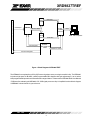
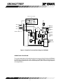
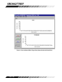
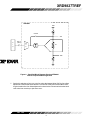
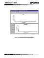
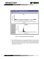
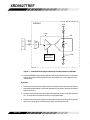
XRD9827TREF
May 1999-2
XRD9827TREF
USER MANUAL
TOSHIBA CIS 36-BIT COLOR
SINGLE LINE SCANNER
Rev. 1.00
EXAR Corporation, 48720 Kato Road, Fremont, CA 94538 • (510) 668-7000 • FAX (510) 668-7017
XRD9827TREF
EVALUATION KIT PART LIST
z
z
z
z
z
XRD9827TREF CIS 36-Bit Color Single Line Scanner
XRD9827TREF User Manual
SenseIt 1.0 Software Installation Diskettes (3)
XRD9827 Data Sheet
Scan Targets (Black, White, Color)
FEATURES
z One line scanning functionality of XRD9827 with TOSHIBA 600DPI CIS
(Contact Image Sensor)
z Easy to use with most personal computers through Parallel Port Interface
z Simple way of loading the Serial Port of XRD9827 to adjust gain and offset
z Software SenseIt 1.0 to view single line scan
z Optimized PCB Layout with Four Layers
SYSTEM REQUIREMENTS
z
z
z
z
Intel 486 compatible computer with Windows 95 operating system
8 MBytes system memory
25-pin D-shape parallel port receptacles
3 1/2” floppy disk drive
INTRODUCTION
The XRD9827TREF is a demo system which includes a PCB design with a TOSHIBA
CIPS218MC600 600DPI Color Contact Image Sensor (CIS). It demonstrates how to interface
a CIS with EXAR’s XRD9827, a 12-bit Linear CIS/CCD Sensor Signal Processor to output a
single line scan and display the offset and gain corrected amplitude of each of the three colors.
The XRD9827TREF is designed to provide a signal path for the CIS output signals to be
processed, digitized by the XRD9827 and transmitted to a personal computer. There are no
software algorithms or hardware implementations to adjust for color response.
The XRD9827TREF board is loaded with the XRD9827, an Altera MAX7128SLC84 FPGA, two
FIFO SRAMs and peripheral circuits for the CIS. The MAX7128, which is a FieldProgrammable Gate Arrays (FPGA) provides timing signals to the XRD9827, the SRAMs and
the CIS. It also programs the XRD9827 to operate in the correct mode and adjust for gain and
offset values. The XRD9827 processes the analog output from the CIS sensor, level-shifts
and converts the signal into 12-bit digital codes. The SRAMs gate the digitized data from the
XRD9827 and store the data temporarily. Controlled by the software, the SRAMs send the
data through a parallel port connection to the PC and histograms of raw data are displayed
on the monitor using the SenseIt software. A block diagram of the XRD9827TREF is shown
below in Figure 1.
Rev. 1.00
2
XRD9827TREF
8-Bit Data
TOSHIBA CIPS218MC600 600DPI COLOR CIS
FIFO
SRAM
CIS Output
XRD9827
Parallel
Port DB25
Connector
6-Bit Bus Nibble
INTEL 486 Compatible
FIFO
SRAM
Control Signals
Data
8-Bit Data
ALTERA
EPM7128SLC84
FPGA
Parallel Port Control
CIS Control Signals
Figure 1. Block Diagram of XRD9827TREF
The XRD9827 is a complete linear CIS or CCD sensor signal processor on a single monolithic chip. The XRD9827
includes a high speed 12-Bit ADC, a 6-Bit Programmable Gain Amplifier with gain adjustment of 1 to 10 and an
8-Bit programmable input referred offset calibration range of 800 mV. Please see the XRD9827EVAL User Manual
/ PCB board for evaluating the XRD9827 CIS / CCD signal processor chip. A simplified functional block diagram
of XRD9827 is shown below for your reference.
Rev. 1.00
3
XRD9827TREF
Biasing Circuit for CANON
CIS
VBG
AVDD
Power
Down
GRN
CLAMP
RED
S/H
DVDD
&
+
3-1
VREF+
MUX
VRT
BUFFER
BLU
12
_
RL12-BIT
ADC
PGA
VDCREF
VDCEXT
DATA
I/O
PORT
8
DB7:0
VRB
INT/EXT_VDCREF
6
G<5:0>
DGND
CLP
6-BIT GAIN
REGISTERS
Power
DC/AC
R
G
Down
B
8-BIT DAC
AVDD
AGND
AGND
AGND
8
O<7:0>
CIS/CCD
8-BIT OFFSET
REGISTERS
VRT
CCD
CIS
R
G
B
TIMING &
SYNCH
CLAMP
ADCCLK
CONTROL LOGIC
Figure 2. Simplified Functional Block Diagram of XRD9827
OPERATIONAL PROCEDURE
The routine listed below will first calibrate the photo response of the CIS using the XRD9827
by optimizing its offset and gain. After calibration, the XRD9827TREF can be used to scan
any color target to show CIS non-color corrected response. (Color correction is typically done
in the digital ASIC.)
Rev. 1.00
4
XRD9827TREF
How to Run the XRD9827TREF Demonstration
1. Make sure the computer is powered off and the AC power adapter is disconnected from
a wall outlet
2. Connect the parallel port cable to the printer port of the computer
3. Connect the AC power adapter into a wall outlet
4. Turn on the computer and activate Windows 95
Loading EXAR Software
5.
6.
7.
8.
Load the diskette labeled SenseIt 1.0 Disk # 1 into the floppy drive
Select the Start menu in the program manager and choose RUN
Inside the small pop-up window, type: A:\setup
Follow the instructions to finish software installation
Parallel Port Configurations
1. Confirm the parallel port address as follows:
a. Select the Start Menu, choose Settings, then choose Control Panel
b. From the Control Panel window which pops up, double-click on System
c. In the System Properties window, select Device Manager
d. From the Device Manager window, double-click on Ports (COM & LPT)
e. Double-click on Printer Port (LPT1). If you can not find it, please goto Step 2
f. From the pop-up window, select Resources
g. Verify the Input/Output Range is set to 0378 - 037F
h. If the range is not correct, clear the Use Automatic Settings check box by clicking it
i. Choose correct address which is 0378 by default and click OK
j. Re-start the computer as advised
2. If you do not have a Printer Port configured on your computer, please follow the steps listed
below:
a. From the Control Panel window which pops up, double-click on Add New Hardware
b. From the pop-up window, click the Next > button
c. Select ‘No’ when prompted for ‘Do you want Windows to search for your new
hardware?’, then click the Next > button
d. Choose Ports (COM & LPT), then click the Next > button
e. Choose Printer Port, then click the Next > button
f. Make a note of the Input/Output Range of Printer Port of your computer and click OK.
You will use these values later when configure the SenseIt software
g. Re-start the computer as advised
Rev. 1.00
5
XRD9827TREF
D D D D D D D D S S S
0 1 2 3 4 5 6 7 0 1 2
NOT
USED
0
1
Figure 3. Dip Switches Set to Value [110 01000000] to Reset XRD9827
Offset Adjustment With a Black Target
1. Set the dip switches located on the side panel of the scanner to [110 01000000] as shown
in Figure 3 and push the Serial Port button which is located on the front panel of the demo
system. This will reset the XRD9827.
2. Select the Start Menu, choose Programs, then choose SenseIt icon
3. A window will pop up as shown below. The upper window shows the plot of captured data
and the lower window shows the histogram of data. Figure 4 shows the pop-up window when
SenseIt is first started.
4. Select SETUP from the pull-down menu and choose I/O ADDRESS. In the window that pops
up, type in the Input/Output Range of Printer Port of your computer. The default setting is
378H.
5. Select SETUP again from the pull-down menu and choose PIXEL NUMBER. In the pop-up
window, type in 5148 which is the number of pixels of one line.
6. Pick the black target out from the kit and put it on a flat area. Place the XRD9827TREF on
top of the black target with the CIS sensor facing downwards. Set the dip switches to [110
00001100] and then push the Serial Port button. This configures the XRD9827 to operate
in a AC Coupled CCD mode since output signal of TOSHIBA CIS is similar to CCD
waveform. From the CAPTURE menu select SNAP SHOT (or simply press CTRL and B
buttons simultaneously) for a single line scan of the black target. A typical result of a black
target scan is shown in Figure 5.
Rev. 1.00
6
XRD9827TREF
Figure 4. SenseIt Software Window Before Scanning
Rev. 1.00
7
XRD9827TREF
Figure 5. Non-calibrated Black Target Scan (Output Codes Are Below Zero)
Rev. 1.00
8
XRD9827TREF
XRD9827
VDD
CLAMP
VRT
C
PIN 19
(RED)
I
S
M
U
X
RL
VRB
Figure 6. Simplified Block Diagram Showing XRD9827
with AC Coupled CCD Configuration
7.
Set the dip switches to [001 01011000] to select the internal offset DAC for fine offset
adjustment. Push the Serial Port button. From the CAPTURE menu select SNAP SHOT.
A typical result of the fine offset adjustment is shown below. Please notice that the black
code value has moved up to just above zero.
Rev. 1.00
9
XRD9827TREF
Figure 7. Black Target Scan After Fine Offset Adjustment
Rev. 1.00
10
XRD9827TREF
XRD9827
VDD
CLAMP
VRT
C
PIN 19
(RED)
I
S
M
U
X
RL
8-BIT
OFFSET
DAC
VRB
Figure 8. Simplified Block Diagram Showing Fine Offset Adjustment by XRD9827
8. Switch the black target to the enclosed white target. From the CAPTURE menu select
SNAP SHOT for a single lline scan of the white target. A typical result of a white target is
shown below.
Rev. 1.00
11
XRD9827TREF
Figure 9. White Target Scan Without Gain Adjustment
10. Set the dip switches to [000 00111100] to select the desired gain. Push the Serial Port
button. From the CAPTURE menu select SNAP SHOT. The gain should move the output
of the CIS to almost full scale. Please refer to data sheet for further gain adjustment and
optimal values of dip switches for your scanner. A typical result of the white target with
gain adjustment is shown below.
Rev. 1.00
12
XRD9827TREF
Figure 10. White Target Scan After Gain Adjustment
Rev. 1.00
13
XRD9827TREF
XRD9827
VDD
CLAMP
VRT
C
I
S
PIN 19
(RED)
M
U
X
PGA
6-BIT GAIN
REGISTER
RL
VRB
Figure 11. Simplified Block Diagram Showing Gain Adjustment by XRD9827
11. Once the XRD9827 has been fully calibrated, any target can be scanned. For example:
Scan a gray scale to demonstrate the stair step response or a color target for color
responsitivity.
Important:
1. If at any time an unexpected result is shown or the demo system seems to not working,
please pull the AC adapter out from the wall outlet to cycle power. Start the procedures
again from Step 11.
2. Keep the scanner away from other electrical equipment, power cords, light dimmers,
etc., as stray electrical fields can end up in the digitized data.
3. Switch off all unnesscessary light sources and place the scanner flat on the image, this
can prevent stray light from entering the sensor and disrupt the scan.
Rev. 1.00
14
DGND
0.1uF
C31
DVDD
Rev. 1.00
15
POWERJAC
K
J1
10K 10K
R42 R43
UNUSED
LOGIC
3
11
74HC04
7
DGND
10uH
L2
C9
470nF
1
IN
U10
G
N
DGND
2
OUT
LM7809-9
AGND
2
3
gt
TP1
OPEN
74HC04
R36
U9B
4
CISOUT
1
16
17
18
1uF
C33
+9V
C32
100pF
19
0.1uF
1uF
AGND
C4
C3
74HC04
U9E
10
U9F
12
13
14
15
AGN
D
DVD
D
DGN
D
AVDD
DIODE
D1
U3
IN
0.22uF
C10
1
IN
U2
13
11
12
9
8
7
6
5
4
3
2
14
20
10
1
2
OUT
OUT
LM7805-5
3
LM7805-5
DGND
G
N
G
N
2
AGND
0.22uF
C7
1
XRD982
7
VDCEX ADCCL
KCLAM
T
P
SYNC
H
DB7/L
DB6/SDAT
D
GRN ADB5/SCL
DB4
K
DB3
BLU
DB2
DB1
DB0
RED
VREF+
U1
3
0.01uF
C2
0.47uF
C11
0.1uF
C8
DVDD
OPEN
L1
AVDD
SYNC
ADCCLK
CLP
DB7/LD
DB6/SDATA
DB5/SCLK
DB4
DB3
DB2
DB1
DB0
AVDD
0.01uF
AGND
0.1uF
DGND
C6
C5
0.1uF
C1
DVDD
1K
R1
DGND
Date:
Size
B
Title
XRD9827REF_TOSHIBA
CIS
Tuesday, December 15, 1998 Sheet
XRD9827TREF REFERENCE
BOARD
Document Number
1
of
3
GO TO LED ON
CASE OF
THE
SCANNER
HEADER 2
1
2
JP1
H:\PROJECT\ORCADWIN\9827\9827_TOS\9827T_RA.DS
N
DVDD
POWER
CIRCUIT
SUPPLY
S
Rev
A
XRD9827TREF
XRD9827TREF
U6
7
8
10
11
12
13
14
15
DB0
DB1
DB2
DB3
DB4
DB5/SCLK
DB6/SDATA
DB7/LD
DVDD
LWCLK
O7
O6
O5
O4
O3
O2
O1
O0
READY
J2
STROBE
O0
O1
O2
O3
O4
O5
O6
O7
CY7C4261
RCLK
U8
30
31
32
1
2
3
4
5
6
DGND
DVDD
C21
0.1uF
7
8
10
11
12
13
C22
0.1uF
14
15
DGND
AVDD
D8
DVDD
D7
29
D6
RS*28
D5
WEN1*27
D4
WCLK26
D3
WEN2*
D2
D1 LSB
24
D0
Q823
Q722
PAF*
Q621
PAE*
Q520
REN1*
Q419
RCLK
Q318
REN2*
Q217
OE*
Q116
Q0
EF*
9
FF*
GND
25
D8
DVDD
D7
29
D6
RS*28
D5
WEN1*27
D4
WCLK26
D3
WEN2*
D2
D1 MSB
24
D0
Q823
Q722
PAF*
Q621
PAE*
Q520
REN1*
Q419
RCLK
Q318
REN2*
Q217
OE*
Q116
Q0
EF*
9
FF*
GND
1
2
3
4
5
6
7
8
9
10
11
12
13
14
15
16
17
18
19
20
21
22
23
24
25
AUTOFD
RESET
INIT
9
DGND
DVDD
25
U9D
74HC04
8
30
31
32
1
2
3
4
5
6
DB25
DGND
RESET
WEN1
MWCLK
ACK
O7
O6
O5
O4
O3
O2
O1
O0
O[7:0]
DGND
CY7C4261
DVDD
+9V
C24
1uF
C25
0.1uF
C26
0.01uF
AVDD
14
U7A
R22
C28
1
2
0.1uF
7
74HC04
AGND
U7B
DGND 3
4
R26
10K
Q1
NPN
10K
R39
CISOUT
JP3
Q2
NPN
1
2
3
4
5
6
7
8
9
10
11
12
74HC04
RLED
GLED
BLED
U7C
5
R27
330
10K
6
R40
Q3
NPN
74HC04
DGND
U9C
5
CISCLP
CISRST
CISCLK
SP
6
74HC04
DVDD
330
R44
R41
100
DGND
U7F
13
12
74HC04
C30
330
R29
GLED
RLED
BLED
LEDCA (ANODE)
NO CONNECT
RS
CISCLK
SP
DGND
AVDD
DVDD
CISOUT
C29
0.1uF
TOSHIBA CIPS218MC600 CIS
+9V
C34
0.1uF
DGND
AGND
10uF
100
DGND
U7E
11
R30
74HC04
100
H:\PROJECT\ORCADWIN\9827\9827_TOS\9827T_RA.DSN
Title
XRD9827TREF REFERENCE BOARD
U7D
9
DGND
10
8
74HC04
R31
Size
B
100
Date:
Rev. 1.00
16
Document Number
XRD9827REF_TOSHIBA CIS
Tuesday, December 15, 1998
Rev
A
Sheet
3
of
3
XRD9827TREF
DVDD
DVDD
JP2
1
2
3
5
D7
6
D8
DGND
8
D9
9
D6
10
READY
11
D10
DVDD
24
23 D10
22 D9
21 D8
20 D7
19 D6
18 D5
17 D4
16 D3
15 D2
14 D1
13 D0
12
RESET
S1
1
2
3
4
5
6
7
8
9
10
11
12
15
R2
R3
R4
R5
R6
R7
R9
R10
R11
R12
R13
2.2K
2.2K
2.2K
2.2K
2.2K
2.2K
2.2K
2.2K
2.2K
2.2K
2.2K
16
D5
17
D4
18
D3
20
D2
21
D1
R14
33
R15
33
22
MWCLK
SW DIP-12
24
DGND
25
LWCLK
27
28
WEN1
U9A
29
2
1
SPORTN
SYNC
30
31
74HC04
33
34
35
DVDD
36
37
C14
C15
C16
10uF
0.1uF 0.1uF
C17
C18
C19
C20
C27
ACK
39
0.01uF 0.01uF 0.01uF 0.01uF 0.1uF
40
R20
33
41
RCLK
DGND
44
45
78
66
53
43
38
TD0
IO2
TD1
IO3
TMS
IO4
R33
R34
R35
1K
1K
1K
1K
DVDD
TCK
71
1 10
2 9
3 8
4 7
5 6
14
23
62
HEADER 5X2
IO5
IO6
IO58
IO7
IO57
IO8
IO56
IO9
IO55
IO10
IO54
IO11
IO53
IO12
IO52
IO13
IO51
EPM7128SLC84
IO14
IO50
IO15
IO49
IO16
IO48
IO17
IO47
IO18
IO46
IO19
IO45
IO20
IO44
IO21
IO43
IO22
IO42
IO23
IO41
IO24
IO40
IO25
IO39
IO26
IO38
IO27
IO37
IO59
IO36
IO28
IO35
IO29
IO34
IO30
IO33
IO31
IO32
IO60
1
46
R32
S2
IO1
82
4
D0
72
1uF
59
C13
0.1uF
GCLK1
47
C12
OE1/INPUT
42
84
32
DGND
83
Oscillator
26
HEADER 3
3
19
OUT
4
VCCINT1
VCCIO1
VCCIO2
VCCIO3
VCCINT2
VCCIO4
VCCIO5
VCCIO6
GND
V+
DGND1
DGND2
DGND3
DGND4
DGND5
DGND6
DGND7
DGND8
DGND9
DGND10
NC
7
2
2
1
DVDD
U5
13
U4
SPORTN
3
DVDD
81
DGND
80
79
77
76
75
R18
33
74
R19
33
R16
33
73
70
ADCCLK
CISCLK
CISCLP
DB5/SCLK
69
68
R8
33
R17
33
DB6/SDATA
67
65
DB7/LD
64
63
61
60
58
57
56
55
54
CLP
SP
BLED
RLED
GLED
CISRST
52
51
50
49
48
H:\PROJECT\ORCADWIN\9827\9827_TOS\9827T_RA.DSN
Title
Size
B
ALTERA7128SLC84
DGND
Date:
Rev. 1.00
17
XRD9827TREF REFERENCE BOARD
Document Number
XRD9827REF_TOSHIBA CIS
Tuesday, December 15, 1998
Rev
A
Sheet
2
of
3
XRD9827TREF
NOTICE
EXAR Corporation reserves the right to make changes to the products contained in this publication in order to improve
design, performance or reliability. EXAR Corporation assumes no responsibility for the use of any circuits described
herein, conveys no license under any patent or other right, and makes no representation that the circuits are free of
patent infringement. Charts and schedules contained here in are only for illustration purposes and may vary depending
upon a user’s specific application. While the information in this publication has been carefully checked; no
responsibility, however, is assumed for in accuracies.
EXAR Corporation does not recommend the use of any of its products in life support applications where the failure
or malfunction of the product can reasonably be expected to cause failure of the life support system or to significantly
affect its safety or effectiveness. Products are not authorized for use in such applications unless EXAR Corporation
receives, in writing, assurances to its satisfaction that: (a) the risk of injury or damage has been minimized; (b) the
user assumes all such risks; (c) potential liability of EXAR Corporation is adequately protected under the
circumstances.
Copyright 1999 EXAR Corporation
Datasheet May 1999
Reproduction, in part or whole, without the prior written consent of EXAR Corporation is prohibited.
Rev. 1.00
18