1
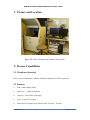
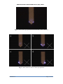
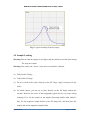
NANOELECTRONICS FABRICATION FACILITY (NFF), HKUST Standard Operating Manual ___________________________________________________________ Park Systems Atomic Force Microscope (AFM) XE-150S Version 1.0 Page 1 of 18 NANOELECTRONICS FABRICATION FACILITY (NFF), HKUST Contents 1. Picture and Location 2. Process Capabilities 2.1 Cleanliness Standard 2.2 Features 2.3 Sample size 3. Contact List and How to Become a Qualified User 3.1 Emergency Responses and Communications 3.2 Training to Become a Qualified User 4. Operating Procedures 4.1 System Description 4.2 Important Cautions 4.3 Turn On the system 4.4 Laser Beam Alignment 4.5 Sample Loading 4.6 Cantilever Approaching 4.7 Measurement 4.8 Sample Unloading 4.9 Data Processing 4.10 Data Analysis 4.11 System Shutdown Version 1.0 Page 2 of 18 NANOELECTRONICS FABRICATION FACILITY (NFF), HKUST 1. Picture and Location Fig 1: XE-150S is located at NFF Phase II Room 2240 2. Process Capabilities 2.1 Cleanliness Standard Prior of any measurement, samples should be submitted to NFF for approval. 2.2 Features Non-Contact Mode AFM Probe size: ~ 10nm in diameter 100 µm × 100 µm XY scan range Up to 12 µm Z scan range Motorized XY sample stage travels entire 150 mm × 150 mm Version 1.0 Page 3 of 18 NANOELECTRONICS FABRICATION FACILITY (NFF), HKUST 2.3 Sample size Up to 6 inch wafer 3. Contact List and How to Become a User 3.1 Emergency Responses and Communications Safety Officer: Mr. Wing Leong CHUNG 2358-7211 & 64406238 Deputy Safety Officer: Mr. Man Wai LEE 2358-7900 & 9621-7708 NFF Phase 2 Technicians: Mr. Li Ho ,or Mr. Chen Yi gong 2358 7896 Security Control Center: 2358-8999 (24hr) & 2358-6565 (24hr) 3.2 Training to Become a Qualified User Please follow the procedure below to become a qualified user. 1. Read all materials on the NFF website concerning this ellipsometer. 2. Send an e-mail to NFF staff requesting operation training. Scheduling can take up to several weeks due to the many requests coming in for this tool. Version 1.0 Page 4 of 18 NANOELECTRONICS FABRICATION FACILITY (NFF), HKUST 4. Operating Procedures 4.1 System Description AFM can be used to image the surface topography with resolution down to nanoscale. The XE-150 consists of four major components: the XE-150 SPM stage with an acoustic enclosure, the control electronics, the computer and the video monitor. In this document, a basic operating procedure is given. For other operating techniques, parameters definitions in the software and other details, please refer to the manuals provided by the Park Systems. 4.2 Important Cautions (1) If the instrument failure while being used, never try to fix the problem by yourself. Please contact NFF staff. (2) Parts of the instrument can be easily damaged. Handle with extreme care. (3) It is easy to break the AFM cantilever. Pay attention to keeping clear of the cantilever from your hands, tweezers and sample during laser beam alignment and sample loading/unloading. (4) Make sure your samples are tidy; especially there should be no sticky residue on the bottom surface. 4.3 Turn On the System (1) Turn on the XY Stage controller and SPM controller. (2) Turn on the computer. (3) Turn on the illuminator. Version 1.0 Page 5 of 18 NANOELECTRONICS FABRICATION FACILITY (NFF), HKUST (4) Open the door of the acoustic enclosure; switch on the power of the Active Vibration Isolation System. (5) Turn on the vacuum pump for sample stage vacuum. (6) After the computer boots up, double click XEC icon to open the CCD vision window for the optical microscope. Wait unit the window is opened. The window displays the actual view from the optical microscope. Then double click the XEP icon to open data acquisition program for XE-150S. (7) The “Frequency Sweep” window will be displayed. Click on “OK” (8) Click on the icon . The “Session Manager” window will be displayed. In the field of “Location”, enter “c:\spmdata\NFFxxxx” where xxxx is your project number. Also enter a name for the “Session Name”. (9) Click on the icon . The “Preferences” window will be displayed. Click on “Filename”. In the field of “Filename Format”, enter a filename. Click on “OK” (10) Check the icon is pressed down. (11) Find NFF staff to help install your AFM cantilever. 4.4 Laser Beam Alignment Warning: Don’t move the “Focus” stage down to and below 1000µm. (1) With the help of the CCD vision, in the “Motors” control window, adjust the “Focus” so that the backside of the cantilever can be viewed clearly. (2) Then adjust the two laser aligning screws located on the upper part of the XE-150S head to move the laser spot to the tip of the cantilever as shown in Fig. 2. Fig. 3 shows that the laser spot deviates from the correct position to a) up, b) down, c) left and d) right. Version 1.0 Page 6 of 18 NANOELECTRONICS FABRICATION FACILITY (NFF), HKUST Fig. 2: correct laser spot position on the backside of the cantilever Fig. 3: some incorrect cases of laser spot position Version 1.0 Page 7 of 18 NANOELECTRONICS FABRICATION FACILITY (NFF), HKUST (3) Adjust the two screws for the steering mirror located on the front side of the head to maximize the A+B signal first (In general, A+B value will be more than 4V). To keep maximizing the A+B signal, at the same time position the laser beam (displayed as red dot on the screen) to the centre of the PSPD so that both A-B and C-D signals are within ±0.5V. (4) Click on the “NCM ASetup” button. The “Frequency Sweep” window will be displayed. Click on the grid area and scroll the mouse to make the scale interval being 500nm. The frequency spectrum of the cantilever should look like the one show in Fig. 4. Fig. 4: typical frequency spectrum of the non-contact cantilever (Model: ACTA). First, drag the red cross to set a drive frequency. In general, it should be set within the typical range as shown in Fig. 5. Secondly, drag the red horizontal line to set a set point. In general, the set point should be set below the red cross where the vertical distance between the red cross and the red line is from 400nm to 1000nm (Note that the larger the distance, the larger the feedback. But it may result in larger noise.). Then click on “OK” Version 1.0 Page 8 of 18 NANOELECTRONICS FABRICATION FACILITY (NFF), HKUST Fig. 5: typical working frequency range. 4.5 Sample Loading Warning: Beware that the sample is too high to hit the cantilever and the head during XY stage movement. Warning: Don’t move the “Focus” stage down to and below 1000µm. (1) Fully lift the Z Stage. (2) Unload the XY Stage. (3) For 4 to 6 inch wafers, place directly on the XY Stage. Apply vacuum to fix the wafer. (4) For small sample, you may try to place directly on the XY Stage without the vacuum. However, the noise of the topography signal may be very large during scanning. If so, fix the sample on the sample disk using double sided adhesive tape. Fix the magnetic sample holder to the XY Stage first, and then place the sample disk on the magnetic sample holder. Version 1.0 Page 9 of 18 NANOELECTRONICS FABRICATION FACILITY (NFF), HKUST (5) Move the XY Stage so that the sample is aligned roughly under the cantilever. (6) Gradually move the Z Stage down until the distance between the sample and the cantilever is around 1mm to 2mm. (Noted that during the Z Stage moving down towards the sample, you can adjust the XY Stage as well to make sure the sample is just under the cantilever.) (7) From the Active Vibration Isolation System’s front panel, press button “E” enable the isolation. The red LED of “ISOL. ON” will be on and the small LCD panel will display “ISOLATION ENABLED”. (8) Close the acoustic enclosure. 4.6 Cantilever Approaching Warning: Don’t move the “Focus” stage down to and below 1000µm. (1) This first thing is to get to know the separation between the cantilever and the sample. The following suggests one of the methods. Method 1: (a) Move down the “Focus” to try to view the image of the cantilever reflected from the sample. For example, Fig. 7 shows an image of the cantilever reflected from a bare Si wafer surface. Fig. 6 shows its real object for comparison. (b) Write down the focus distance F(um) for the image and the focus distance F(um) for the real cantilever. Subtract the focus distance for the real cantilever by the focus distance for the image. And dividing the subtracted value by 2 will give the separation between the cantilever and the sample. Version 1.0 Page 10 of 18 NANOELECTRONICS FABRICATION FACILITY (NFF), HKUST Fig. 6: the real object of the cantilever. Fig. 7: the image of the cantilever of Fig. 6. Version 1.0 Page 11 of 18 NANOELECTRONICS FABRICATION FACILITY (NFF), HKUST (2) Move the Z Stage down so that the separation between the cantilever and the sample is about 100µm. (As it is easy to make collision of the cantilever to the sample carelessly, it is suggested that apply several moves in approaching to the sample. Says if the initial separation is 2000µm, it is better to move down 1000µm first. Then check the separation again.) (3) If there are patterns in the sample, move “Focus” to the sample surface so that the patterns can be viewed. Adjust XY Stage to place the cantilever over the location of interest. (4) Move “Focus” back to the cantilever. (5) Enter the “Scan Size” to zero, “Scan Rate” to 0.5Hz, and “Z Servo Gain” to 1. (6) Adjust the PSPD signal again if it drifted. After PSPD signal is adjusted, click on “NCM ASetup” to set the drive frequency and set point again. (7) Click on “Approach” to let the computer automatically bring the cantilever to the sample surface. Warning: After the cantilever reached the sample surface, (1) don’t move the Z Stage down; (2) don’t adjust the Focus; (3) don’t move the XY Stage; (4) don’t click on “NCM ASetup”. 4.7 Measurement (1) Look at the Topography line traces. Since the Scan Size is set as zero now, it shows the traces of zero scan (see Fig. 8) Version 1.0 Page 12 of 18 NANOELECTRONICS FABRICATION FACILITY (NFF), HKUST Fig. 8: Zero scan traces. Check that the zero scan traces are straight enough (no matter leveling of the traces and neglect the amplitudes over the straight traces first). Then, check also the amplitudes are small enough for your application. In Fig. 8, the amplitude are about 2Å. (If the traces are not straight or the amplitudes are too large, don’t perform scan. Move the Z-stage up so that the separation between the cantilever and the sample is about 100µm. Click on “NCM ASetup”. Try another drive frequency or/and set point. Approach again to see if it helps. Otherwise, the cantilever may need to be replaced.) (2) Enter the “Scan Size”. (It is suggested that start from 1µm first if you don’t know much about the features of your sample) (3) Adjust the “Z Servo Gain” in order to make the two line traces matching each other and repeatable. You can increase the gain until there is no oscillation present. (4) Adjust the “Offset X” and “Y” if necessary. (5) Click on the “Start” or “Scan Here” to start the measurement. Version 1.0 Page 13 of 18 NANOELECTRONICS FABRICATION FACILITY (NFF), HKUST 4.8 Sample Unloading (1) Enter the “Scan Size” to zero. (2) Move the Z-stage up so that the separation between the cantilever and the sample is about 100µm. (3) Click on “Lift Z”. (4) Open the door of the acoustic enclosure. From the Active Vibration Isolation System’s front panel, press button “E” to disable the isolation. The red LED of “ISOL. ON” will be off and the small LCD panel will display “ISOLATION DISABLED”. (5) Unload the XY Stage. (6) Turn off the vacuum if the vacuum has been applied. (7) Remove the sample. 4.9 Data Processing The first step is flattening. Three examples will be given here. Flattening Example 1: Grid patterns (1) Double click XEI icon to open the data analysis software. (2) Open a data file “c:\spmdata\Examples\example1.tiff”. (3) Select “Process>Flatten” from the Menu bar. (4) Click on “ ” to select entire region. (5) In the parameters setting, select “Whole” for the Scope; “X Axis” for the Orientation; “1” for the Regression Order. (6) Click on “Execute”. (7) Change Orientation from “X Axis” to “Y Axis”. Version 1.0 Page 14 of 18 NANOELECTRONICS FABRICATION FACILITY (NFF), HKUST (8) Click on “Execute” again. (9) Click on “OK”. Example 2: Bare silicon (1) In the XEI, open a data file “c:\spmdata\Examples\example2.tiff”. (2) Select “Process>Flatten” from the Menu bar. (3) Click on “ ” to select entire region. (4) In the parameters setting, select “Line” for the Scope; “X Axis” for the Orientation; “1” for the Regression Order. (Note that Orientation must be set the same as the fast scan direction during measurement for “Line” Scope. In this example, the fast scan direction is X axis.) (5) Click on “Execute”. (6) Click on “OK”. Example 3: Surface with large particles (1) In the XEI, open a data file “c:\spmdata\Examples\example3.tiff”. (2) In this example, the data was flattened once according to the Step (4) of Example 2. Some dark shadows (regions with lower height) are seen near some large and tall particles as shown in Fig. 9. Version 1.0 Page 15 of 18 NANOELECTRONICS FABRICATION FACILITY (NFF), HKUST Fig.9 Click on “ ” to select entire region. (3) In the Histogram, drag the left cursor and place it at 1nm in order to unselect the regions where the height is larger than 1nm. (4) In the parameters setting, select “Line” for the Scope; “X Axis” for the Orientation; “1” for the Regression Order. (5) Click on “Execute”. (6) Click on “OK”. The result is shown in Fig. 10. Fig. 10 Version 1.0 Page 16 of 18 NANOELECTRONICS FABRICATION FACILITY (NFF), HKUST 4.10 Data Analysis Line Analysis (1) In the XEI, select “Analysis>Line”. (2) From the toolbar at the right hand side of the image, select slanted line or x-axis line or y-axis line first. Click on the graph and a line will be shown on the image. Drag the line to the line of interest. (3) A corresponding Line Profile is shown on the right of the screen. And Statistics such as roughness of the line are shown on the bottom. (4) Repeat Step (2) for adding second line if necessary. To display profiles for both lines at the same time, simply click on any area of the image other than the two lines. (5) Right click on the line profile to show a menu of useful items for doing some measurement on the profile. Select them if necessary. (6) Export the screen by selecting “File>Export”. Enter the file name and also the file type (.png or .jpg, or .bmp). Click on “Save”. Region Analysis (1) In the XEI, select “Analysis>Region”. (2) From the toolbar at the right hand side of the image, you can select Entire Region. Or click on the Inclusion icon first, and then select Square or the Ellipse or the Polygon; click on the graph and adjust the size; place it on the area of interest. Statistics are shown on the bottom. (3) Export the screen by selecting “File>Export”. Version 1.0 Page 17 of 18 NANOELECTRONICS FABRICATION FACILITY (NFF), HKUST 3D (1) In the XEI, select “Analysis>3D”. (2) Drag the 3D image for adjusting the viewing angle. (3) Export the screen by selecting “File>Export”. 4.11System Shutdown (1) Make sure the sample has been removed. If not, follow steps of “Sample Unloading”. (2) Shutdown the computer. (3) Turn off the XY Stage controller and SPM controller. (4) From the Active Vibration Isolation System’s front panel, press button “↑” for several times until the LCD displays “SYSTEM UNLOCKED”. Then press button “ “to lock the system. Wait for the locking mechanism finish. The LCD panel will display “SYSTEM LOCKED”. Turn off the power of the Active Vibration Isolation System. (5) Close the door of the acoustic enclosure. (6) Turn off the illuminator. (7) Turn off the vacuum pump. Reference: (1) XE-150 User’s Manual by Park Systems Corporation. (2) XEP Software Manual by Park Systems Corporation. (3) XEI Software Manual by Park Systems Corporation. Version 1.0 Page 18 of 18