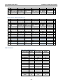
1
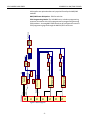
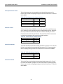
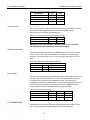
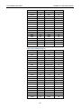
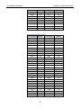
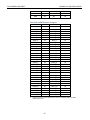
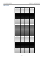
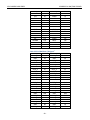
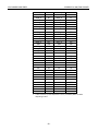
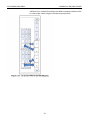
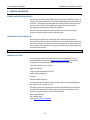
Carrier Card Series VPX4820/VPX4820CC VPX XMC/PMC Carrier USER’S MANUAL ACROMAG INCORPORATED 30765 South Wixom Road Wixom, MI 48393-7037 U.S.A. Tel: (248) 295-0310 Fax: (248) 624-9234 Copyright 2014, Acromag, Inc., Printed in the USA. Data and specifications are subject to change without notice. 8501-010A VPX CARRIER CARD SERIES VPX4820 PCIe XMC/PMC CARRIER Contents 1. 2. GENERAL INFORMATION ............................................................................................................... 4 KEY VPX4820 FEATURES ................................................................................................................ 4 PREPARATION FOR USE ................................................................................................................. 6 UNPACKING AND INSPECTION ....................................................................................................... 6 CARD CAGE CONSIDERATIONS .................................................................................................. 6 Board Configuration ................................................................................................................. 6 JUMPERS ...................................................................................................................................... 7 PCIe Lane Configuration............................................................................................................ 7 PCie Upstream Port Select ........................................................................................................ 8 PCie Gen 1 Force ...................................................................................................................... 8 PCie NT Port Enable .................................................................................................................. 8 PCie NT Port Select................................................................................................................... 8 +3.3_AUX Power ...................................................................................................................... 9 JTAG Reference Power.............................................................................................................. 9 Clock Settings........................................................................................................................... 9 I2C PROGRAMMING....................................................................................................................... 9 NVROM ..................................................................................................................................10 LED’s ...........................................................................................................................................10 BACKPLANE KEY ...........................................................................................................................10 CONNECTORS ..............................................................................................................................10 VPX Connectors.......................................................................................................................12 PMC Connectors......................................................................................................................14 XMC Connectors......................................................................................................................18 3. 4. 5. FIELD GROUNDING CONSIDERATIONS ...........................................................................................21 VPX CONNECTIVITY ......................................................................................................................22 VITA 65 PROFILES.........................................................................................................................22 REAR I/O......................................................................................................................................22 SERVICE AND REPAIR....................................................................................................................24 SERVICE AND REPAIR ASSISTANCE.................................................................................................24 PRELIMINARY SERVICE PROCEDURE..........................................................................................24 WHERE TO GET HELP ....................................................................................................................24 SPECIFICATIONS...........................................................................................................................25 PHYSICAL.....................................................................................................................................25 Physical Configuration .............................................................................................................25 Connectors .............................................................................................................................25 Jumpers..................................................................................................................................25 - 2- VPX CARRIER CARD SERIES VPX4820 PCIe XMC/PMC CARRIER POWER........................................................................................................................................25 XMC/PMC Power.....................................................................................................................26 Power Dissipation....................................................................................................................26 6. PCIe BUS COMPLIANCE.................................................................................................................28 PCI BUS COMPLIANCE...................................................................................................................29 XMC/PMC Slot Selection...............................................................................................................29 Rear I/O.......................................................................................................................................29 ENVIRONMENTAL ........................................................................................................................29 Certificate of Volatility..................................................................................................................30 Revision History ...........................................................................................................................30 The information contained in this manual is subject to change without notice. Acromag, Inc. makes no warranty of any kind with regard to this material, including, but not limited to, the implied warranties of merchantability and fitness for a particular purpose. Further, Acromag, Inc. assumes no responsibility for any errors that may appear in this manual and makes no commitment to update, or keep current, the information contained in this manual. No part of this manual may be copied or reproduced in any form, without the prior written consent of Acromag, Inc. IMPORTANT SAFETY CONSIDERATIONS It is very important for the user to consider the possible adverse effects of power, wiring, component, sensor, or software failures in designing any type of control or monitoring system. This is especially important where economic property loss or human life is involved. It is important that the user employ satisfactory overall system design. It is agreed between the Buyer and Acromag, that this is the Buyer's responsibility. - 3- VPX CARRIER CARD SERIES VPX4820 PCIe XMC/PMC CARRIER 1. GENERAL INFORMATION The VPX4820 card is a 6U VPX non-intelligent XMC/PMC carrier board designed for PCIe bus connection to the VPX Expansion Plane. The board supports up to a 16x PCIe connection that is selectable via jumpers. The carrier enables the use of XMC and PMC mezzanine I/O modules. The carrier card acts as an adapter to route PCIe bus signals between the PCIe bus of your backplane and either P15 connector of an XMC module card or P11 and P12 of a PMC Card. Access to rear I/O is provided through connections to the backplane. XMC and PCM modules with front I/O can be accessed though the front mounting bracket. The VPX4820 series is a 6U VPX Non-Intelligent XMC/PMC carrier board designed for 4x/8x/16x PCIe bus connection. The carrier card uses a PLX Technology® PCIe Switch Chip (PEX 8632) and IDT Technology® PCIe to PCI Bridge Chip (TSI384) to interface between the VPX PCIe bus and one XMC/PMC mezzanine I/O module card. Model VPX4820 is an air-cooled product which can be used for front and rear I/O XMC/PMC mezzanine modules. Model VPX4820CC is an extended temperature conduction-cooled product which supports all Acromag FPGA modules. It only supports Rear I/O. Model Board Size Operating Temperature (Length) Range VPX4820 6U 0 to +70C VPX4820-CC 6U -40 to +85C1 1. See Power Specifications for further information including power rating. 2. Both boards are available in leaded (-L) or lead-free (-LF) version. KEY VPX4820 FEATURES PCI Express Interface: Up to Sixteen PCI Express Gen 1 or Gen 2 lanes are connected to the VPX P2 connecter. This is the Expansion Plane. Lane configuration is jumper selectable. PCI Express Configuration: Jumper selectable for one x16 port, two x8 ports, four x4 ports, or one x8 port and two x4 ports. PCI and PC-X Compliant: Each slot supports up to 133MHz 64 bit PCI-X. Upstream and NT Port Configuration: Selectable via jumper. I/O: Support both Front and Rear I/O. CC model is Rear I/O only. Single Power Supply: The carrier only requires VPX to provide +12V to PS1. The carrier will generate and supply the PMC/XMC modules with +5V and +3.3V. The XMC VPWR pins are connected to +12V. This board can also run off only the VPX PS3 +5V supply. Please contact the factory for details. All - 4- VPX CARRIER CARD SERIES VPX4820 PCIe XMC/PMC CARRIER AUX supplies are optional and are only required if used by the XMC/PMC modules. XMC/PMC Power Dissipation: 25W for each slot. JTAG Programming Header: The VPX4820 carrier includes a programming connector that mates with a Xilinx programmer for programming Acromag FPGA products. Acromag XMC FPGA boards can be configured to route the JTAG programming signals through the XMC P15/P25 connectors. Figure 1 Block Diagram - 5- VPX CARRIER CARD SERIES VPX4820 PCIe XMC/PMC CARRIER 2. PREPARATION FOR USE UNPACKING AND INSPECTION Upon receipt of this product, inspect the shipping carton for evidence of mishandling during transit. If the shipping carton is badly damaged or water stained, request that the carrier's agent be present when the carton is opened. If the carrier's agent is absent when the carton is opened and the contents of the carton are damaged, keep the carton and packing material for the agent's inspection. For repairs to a product damaged in shipment, refer to the Acromag Service Policy to obtain return instructions. It is suggested that salvageable shipping cartons and packing material be saved for future use in the event the product must be shipped. This board is physically protected with packing material and electrically protected with an anti static bag during shipment. It is recommended that the board be visually inspected for evidence of mishandling prior to applying power. The board utilizes static sensitive components and should only be handled at a static-safe workstation. CARD CAGE CONSIDERATIONS Refer to the specifications for loading and power requirements. Be sure that the system power supplies are able to accommodate the power requirements of the carrier board, plus the installed PMC/XMC modules, within the voltage tolerances specified. Adequate air circulation must be provided to prevent a temperature ri se above the maximum operating temperature and to prolong the life of the electronics. If the installation is in an industrial environment and the board is exposed to environmental air, careful consideration should be given to airfiltering. Board Configuration Power should be removed from the board when changing jumper configurations or when installing an XMC or PMC module, cables and field wiring. - 6- VPX CARRIER CARD SERIES VPX4820 PCIe XMC/PMC CARRIER JUMPERS There are three jumper blocks located on the board. The jumper blocks are labeled J1, J2, and J3. Within each jumper block are five jumpers. Jumper one is marked as shown in the diagram above. Refer to Error! Reference source not found. above. The description for each jumper is described in the tables below. The jumper position is OPEN if no jumper is present. The jumper position is SET if a jumper is present across the two pins. For rugged designs all jumpers can be replaced with 0 Ohm resistors. Please contact the factory for details. Figure 2 Jumper and Connector Locations Bold Selections are the factory defaults. PCIe Lane Configuration The VPX P2 PCie lane configuration is selectable via the first and second jumper of J1. Please note that these strapping settings can be overwritten via a I2 C write to the PLX8632. Table 2-1 PCIe Lane Jumper Configuration PCIe Lane Configuration J1-1 J1-2 16x OPEN OPEN 8x-8x SET SET 4x-4x-4x-4x OPEN SET 8x-4x-4x SET OPEN The PCie lane configuration determined the PCIe switch port naming convention. Use Table 2-2 as a reference when selecting the upstream and downstream port.22 Table 2-2 PCIe Port Naming Convention PCIe Lane Configuration Port Naming L0-L3 L4-L7 L8-L11 L12-L15 16x Port 0 8x-8x Port 0 Port 1 4x-4x-4x-4x Port 0 Port 1 Port 2 Port 3 8x-4x-4x Port 0 Port 1 Port 2 - 7- VPX CARRIER CARD SERIES VPX4820 PCIe XMC/PMC CARRIER PCie Upstream Port Select The PCIe Upstream port is selected by the third and forth jumpers of J1. Please note that these strapping settings can be overwritten via a I 2 C write to the PLX8632. Table 2-3 PCIe Upstream Port Jumper Selection PCIe Upsteam Port J1-3 J1-4 0 OPEN OPEN 1 SET OPEN 2 OPEN SET 3 SET SET PCie Gen 1 Force To Force all lanes of the PEX8632 to run at Gen 1 speeds set the fifth jumper of J2. Note only use this setting if the auto-negotiate process fails. Normally this only needs to be used for PCIe devices are were released prior to the finalization of the PCIe 1.0 specification. This will effect all PCIe connections on the board including to the processor and XMC modules. Table 2-4 PCIe Force Gen 1 Jumper Setting PCIe Speed J2-5 Gen 1 SET Gen 2 OPEN PCie NT Port Enable To Enable the NT Port of the PCIe switch, SET the first jumper of J3. The PCIe NT port is selected by the second and third jumpers of J3. Please note that these strapping settings can be overwritten via a I 2C write to the PLX8632. Table 2-5 NT Enabled Jumper Settings NT Port J3-1 Disabled OPEN Enabled Set PCie NT Port Select The PCIe NT port is selected by the second and third jumpers of J3. The NT Port must be enabled via jumpers J3-1 for these jumper to operate properly. Please note that these strapping settings can be overwritten via a I 2 C write to the PLX8632. - 8- VPX CARRIER CARD SERIES VPX4820 PCIe XMC/PMC CARRIER Table 2-6 PCIe NT Port Jumper Selection PCIe NT Port J3-2 J3-3 0 OPEN OPEN 1 SET OPEN 2 OPEN SET 3 SET SET +3.3_AUX Power The 3.3V_AUX power is required for proper operation of this board. For users without this power supply available on the VPX backplane you can alternatively use the onboard generated 3.3V. Table 2-7 +3.3V_AUX Power Select Jumper Settings Source of +3.3V-AUX J3-4 J3-5 Backplane OPEN SET Onboard SET OPEN WARNING! The J3-4 and 5 jumpers should both never be set. This could cause damage to either the board or chassis power supply. JTAG Reference Power The pull-up voltage on the JTAG pins to XMC P15 and P25 can be selected as either +2.5V or +3.3V. Refer to the XMC User’s Manual for proper voltage selection. The forth jumper in J2 is for slot A and the fifth jumper in J1 is for slot B. Table 2-8 JTAG Power Select Jumper Settings JTAG Ref Voltage Slot LOC Setting Slot A J2-4 SET +3.3V OPEN +2.5V Slot B J1-5 SET +3.3V OPEN +2.5V Clock Settings There are several clock options available for the user. These options are set on the first, second, and third jumpers of J2. The default selection is to use the on-board crystal to generate the 100MHz PCIe clock. This frequency is propagated to all parts and XMC modules. Users also have the option to use a clock from the VPX backplane. Note that this must be a 100MHz clock for proper operation. Refer to the table below for jumper settings. Table 2-9 Clock Jumper Settings Global Clock Source J2-1 On Board Crystal OPEN VPX SYSCLK SET Disable all CLK’s OPEN J2-2 OPEN OPEN OPEN J2-3 OPEN OPEN SET I2C PROGRAMMING The PEX8632 PCI switch can alternately be programmed via a simple I 2C bus. The I2C is accessed via the System Bus pins on the VPX backplane. - 9- VPX CARRIER CARD SERIES VPX4820 PCIe XMC/PMC CARRIER Furthermore the I 2C bus is connected to both XMC modules. For further information on programming using the I2C bus contact the factory. NVROM The NVROM signal from the VPX Backplane is routed to the PCIe Switch EEPROM as well as both XMC modules. LED’s The VPX4820 has several status LEDS. Refer to Figure 2 for the location of the LED’s. These LED’s are primarily used for initial power-up status. The table below describes the functionality. Table 2-10 LED LED Color DS1 Green DS2 Red DS3 Red DS4 Red DS5 Red DS6 Red DS7 Red DS8 Red DS9 Red DS10 Green DS11 Green DS12 Green DS13 Green DS14 Green DS15 Green DS16 Red DS17 Green Description All power supplies are good. PMC A Only – PCIe Lane 1 has connected. PMC A Only – PCIe Lane 2 has connected. PMC A Only – PCIe Lane 3 has connected. PMC A Only – PCIe Lane 4 has connected. PMC B Only – PCIe Lane 1 has connected. PMC B Only – PCIe Lane 2 has connected. PMC B Only – PCIe Lane 3 has connected. PMC B Only – PCIe Lane 4 has connected. VPX PCIe Port 0 has successfully connected VPX PCIe Port 1 has successfully connected VPX PCIe Port 2 has successfully connected VPX PCIe Port 3 has successfully connected A Connection has been made to XMC/PMC Slot A. A Connection has been made to XMC/PMC Slot B. Fatal Error (non-recoverable) PCI INTA BACKPLANE KEY The VPX4820 is not keyed and will plug into any VPX backplane. Prior to powerup, verify that VS1 is +12V. Any other voltage on VS1 may damage the board. CONNECTORS Refer to Error! Reference source not found. for connector locations. Connectors on the VPX4820 carrier consist of six VPX Backplane connectors, then 2 XMC connectors, and four PMC connectors for each slot. These interface connectors are discussed in the following sections. - 10 - VPX CARRIER CARD SERIES VPX4820 PCIe XMC/PMC CARRIER J11/J12/J13/J21/J22/J23 ...............PMC PCI signals J14/J25........................................PMC user signals (Rear I/O) J15/J25 ........................................XMC PCIe signals J16/J26 .......................................XMC user signals (Rear I/O) P0 ...............................................VPX Power and system signals. P1…………………………………………………VPX Data Plane. This connector is not populated. P2 ...............................................VPX Expansion plane. This connects to all PCIe lanes. P3/P4..........................................PMC/XMC Slot A Rear I/O. P5/P6 ..........................................PMC/XMC Slot B Rear I/O. - 11 - VPX CARRIER CARD SERIES VPX4820 PCIe XMC/PMC CARRIER VPX Connectors Table 2-11 P0 – VPX Utility Signals Pin A B C D 1 VS2 VS2 VS2 NC 2 VS2 VS2 VS2 NC 3 +5V +5V +5V NC 4 NVMRO P0_SYSRESET GND -12V_AUX 5 I2C_DAT I2C_CLK GND +3.3V_AUX 6 GA0 GA1 GND +12V_AUX 7 JTAG_TRST JTAG_TMS GND JTAG_TDI 8 GND REF_BUS_P REF_BUS_N GND All blue colored cells are Not Used in this design. E +12V +12V +5V GND GND GND JTAG_TDO P0_REFCLK_P Table 2-12 P2 – VPX Expansion Plane Pin A B C D 1 PCIE_L0_RXP PCIE_L0_RXN Gnd PCIE_L0_TXP 2 Gnd PCIE_L1_RXP PCIE_L1_RXN Gnd 3 PCIE_L2_RXP PCIE_L2_RXN Gnd PCIE_L2_TXP 4 Gnd PCIE_L3_RXP PCIE_L3_RXN Gnd 5 PCIE_L4_RXP PCIE_L4_RXN Gnd PCIE_L4_TXP 6 Gnd PCIE_L5_RXP PCIE_L5_RXN Gnd 7 PCIE_L6_RXP PCIE_L6_RXN Gnd PCIE_L6_TXP 8 Gnd PCIE_L7_RXP PCIE_L7_RXN Gnd 9 PCIE_L8_RXP PCIE_L8_RXN Gnd PCIE_L8_TXP 10 Gnd PCIE_L9_RXP PCIE_L9_RXN Gnd 11 PCIE_L10_RXP PCIE_L10_RXN Gnd PCIE_L10_TXP 12 Gnd PCIE_L11_RXP PCIE_L11_RXN Gnd 13 PCIE_L12_RXP PCIE_L12_RXN Gnd PCIE_L12_TXP 14 Gnd PCIE_L13_RXP PCIE_L13_RXN Gnd 15 PCIE_L14_RXP PCIE_L14_RXN Gnd PCIE_L14_TXP 16 Gnd PCIE_L15_RXP PCIE_L15_RXN Gnd All blue colored cells are Not Used in this design. Table 2-13 P3 – PMC SLOT A Rear I/O Pin A B C 1 PMC1_RIO1_N PMC1_RIO1_P Gnd 2 Gnd PMC1_RIO3_N PMC1_RIO3_P 3 PMC1_RIO5_N PMC1_RIO5_P Gnd 4 Gnd PMC1_RIO7_N PMC1_RIO7_P 5 PMC1_RIO9_N PMC1_RIO9_P Gnd 6 Gnd PMC1_RIO11_N PMC1_RIO11_P 7 PMC1_RIO13_N PMC1_RIO13_P Gnd 8 Gnd PMC1_RIO15_N PMC1_RIO15_P 9 PMC1_RIO17_N PMC1_RIO17_P Gnd 10 Gnd PMC1_RIO19_N PMC1_RIO19_P F +12V +12V +5V SM3 GA4 GA2 GND P0_REFCLK_N E G +12V +12V +5V SM2 GAP GA3 JTAG_TCK GND F G PCIE_L0_TXN PCIE_L1_TXP PCIE_L2_TXN Gnd PCIE_L1_TXN Gnd PCIE_L3_TXP PCIE_L4_TXN PCIE_L5_TXP PCIE_L6_TXN PCIE_L7_TXP PCIE_L3_TXN Gnd PCIE_L5_TXN Gnd PCIE_L7_TXN PCIE_L8_TXN PCIE_L9_TXP PCIE_L10_TXN PCIE_L11_TXP Gnd PCIE_L9_TXN Gnd Gnd PCIE_L11_TXN Gnd PCIE_L12_TXN PCIE_L13_TXP PCIE_L14_TXN PCIE_L15_TXP Gnd PCIE_L13_TXN Gnd Gnd PCIE_L15_TXN Gnd D E Gnd Gnd Gnd Gnd F G PMC1_RIO0_N PMC1_RIO0_P Gnd Gnd PMC1_RIO4_N Gnd PMC1_RIO8_N PMC1_RIO2_N PMC1_RIO4_P PMC1_RIO6_N PMC1_RIO8_P PMC1_RIO2_P Gnd PMC1_RIO6_P Gnd Gnd PMC1_RIO12_N Gnd PMC1_RIO16_N PMC1_RIO10_N PMC1_RIO12_P PMC1_RIO14_N PMC1_RIO16_P PMC1_RIO10_P Gnd Gnd PMC1_RIO14_P Gnd Gnd Gnd PMC1_RIO18_N PMC1_RIO18_P Gnd - 12 - Gnd Gnd VPX CARRIER CARD SERIES VPX4820 PCIe XMC/PMC CARRIER Pin A B C 11 PMC1_RIO21_N PMC1_RIO21_P Gnd 12 Gnd PMC1_RIO23_N PMC1_RIO23_P 13 PMC1_RIO25_N PMC1_RIO25_P Gnd 14 Gnd PMC1_RIO27_N PMC1_RIO27_P 15 PMC1_RIO29_N PMC1_RIO29_P Gnd 16 Gnd PMC1_RIO31_N PMC1_RIO31_P All blue colored cells are Not Used in this design. Table 2-14 P4 – XMC SLOT A Rear I/O Pin A B C 1 XMC1_DP05_N XMC1_DP05_P Gnd 2 Gnd XMC1_DP07_N XMC1_DP07_P 3 XMC1_DP09_N XMC1_DP09_P Gnd 4 Gnd XMC1_DP15_N XMC1_DP15_P 5 XMC1_DP17_N XMC1_DP17_P Gnd 6 Gnd XMC1_DP19_N XMC1_DP19_P 7 XMC1_DP01_N XMC1_DP01_P Gnd 8 Gnd XMC1_DP03_N XMC1_DP03_P 9 XMC1_DP11_N XMC1_DP11_P Gnd 10 Gnd XMC1_DP13_N XMC1_DP13_P 11 Gnd 12 Gnd 13 Gnd 14 Gnd 15 Gnd 16 Gnd All blue colored cells are Not Used in this design. Table 2-15 P5 – PMC SLOT B Rear I/O Pin A B C 1 PMC2_RIO1_N PMC2_RIO1_P Gnd 2 Gnd PMC2_RIO3_N PMC2_RIO3_P 3 PMC2_RIO5_N PMC2_RIO5_P Gnd 4 Gnd PMC2_RIO7_N PMC2_RIO7_P 5 PMC2_RIO9_N PMC2_RIO9_P Gnd 6 Gnd PMC2_RIO11_N PMC2_RIO11_P 7 PMC2_RIO13_N PMC2_RIO13_P Gnd 8 Gnd PMC2_RIO15_N PMC2_RIO15_P 9 PMC2_RIO17_N PMC2_RIO17_P Gnd 10 Gnd PMC2_RIO19_N PMC2_RIO19_P 11 PMC2_RIO21_N PMC2_RIO21_P Gnd 12 Gnd PMC2_RIO23_N PMC2_RIO23_P 13 PMC2_RIO25_N PMC2_RIO25_P Gnd D E PMC1_RIO20_N Gnd PMC1_RIO24_N Gnd PMC1_RIO28_N PMC1_RIO20_P PMC1_RIO22_N PMC1_RIO24_P PMC1_RIO26_N PMC1_RIO28_P Gnd PMC1_RIO30_N PMC1_RIO30_P Gnd D F G Gnd PMC1_RIO22_P Gnd Gnd PMC1_RIO26_P Gnd Gnd E F G XMC1_DP04_N Gnd XMC1_DP08_N Gnd XMC1_DP04_P XMC1_DP06_N XMC1_DP08_P XMC1_DP14_N Gnd XMC1_DP06_P Gnd Gnd XMC1_DP14_P Gnd XMC1_DP16_N Gnd XMC1_DP00_N Gnd XMC1_DP16_P XMC1_IO_B19 XMC1_DP00_P XMC1_DP02_N Gnd XMC1_IO_A19 Gnd Gnd XMC1_DP02_P Gnd XMC1_DP10_N XMC1_DP10_P Gnd Gnd XMC1_DP12_N XMC1_DP12_P Gnd Gnd Gnd Gnd Gnd Gnd Gnd Gnd Gnd Gnd D E F G PMC2_RIO0_N Gnd PMC2_RIO0_P PMC2_RIO2_N Gnd PMC2_RIO2_P PMC2_RIO4_N Gnd PMC2_RIO8_N Gnd PMC2_RIO4_P PMC2_RIO6_N PMC2_RIO8_P PMC2_RIO10_N Gnd PMC2_RIO6_P Gnd Gnd PMC2_RIO10_P Gnd PMC2_RIO12_N Gnd PMC2_RIO16_N Gnd PMC2_RIO12_P PMC2_RIO14_N PMC2_RIO16_P PMC2_RIO18_N Gnd PMC2_RIO14_P Gnd Gnd PMC2_RIO18_P Gnd Gnd PMC2_RIO20_N PMC2_RIO20_P Gnd Gnd PMC2_RIO22_N PMC2_RIO22_P Gnd PMC2_RIO24_N PMC2_RIO24_P Gnd - 13 - VPX CARRIER CARD SERIES VPX4820 PCIe XMC/PMC CARRIER Pin A B C D E F G 14 Gnd PMC2_RIO27_N PMC2_RIO27_P Gnd PMC2_RIO26_N PMC2_RIO26_P Gnd 15 PMC2_RIO29_N PMC2_RIO29_P Gnd PMC2_RIO28_N PMC2_RIO28_P Gnd 16 Gnd PMC2_RIO31_N PMC2_RIO31_P Gnd PMC2_RIO30_N PMC2_RIO30_P Gnd All blue colored cells are Not Used in this design. Table 2-16 P6 – XMC SLOT B Rear I/O Pin A B C 1 XMC2_DP05_N XMC2_DP05_P Gnd 2 Gnd XMC2_DP07_N XMC2_DP07_P 3 XMC2_DP09_N XMC2_DP09_P Gnd 4 Gnd XMC2_DP15_N XMC2_DP15_P 5 XMC2_DP17_N XMC2_DP17_P Gnd 6 Gnd XMC2_DP19_N XMC2_DP19_P 7 XMC2_DP01_N XMC2_DP01_P Gnd 8 Gnd XMC2_DP03_N XMC2_DP03_P 9 XMC2_DP11_N XMC2_DP11_P Gnd 10 Gnd XMC2_DP13_N XMC2_DP13_P 11 Gnd 12 Gnd 13 Gnd 14 Gnd 15 Gnd 16 Gnd All blue colored cells are Not Used in this design. D E F G XMC2_DP04_N XMC2_DP04_P Gnd Gnd XMC2_DP06_N XMC2_DP06_P Gnd XMC2_DP08_N XMC2_DP08_P Gnd Gnd XMC2_DP16_N Gnd XMC2_DP00_N XMC2_DP14_N XMC2_DP16_P XMC2_IO_B19 XMC2_DP00_P XMC2_DP14_P Gnd Gnd XMC2_IO_A19 Gnd Gnd Gnd XMC2_DP02_N XMC2_DP02_P Gnd XMC2_DP10_N XMC2_DP10_P Gnd Gnd XMC2_DP12_N XMC2_DP12_P Gnd Gnd Gnd Gnd Gnd Gnd Gnd Gnd Gnd Gnd PMC Connectors Table 2-17 Jx1 PMC PCI Signals Pin Description Number Pin Description TCK 1 -12V GND 3 INTA# INTB# 5 INTC# BUSMODE1# 7 +5V INTD# 9 NC1 GND 11 +3.3VAUX CLK 13 GND GND 15 GNT# REQ# 17 +5V +3.3V 19 AD31 AD28 21 AD27 AD25 23 GND GND 25 C/BE3# AD22 27 AD21 AD19 29 +5V - 14 - Number 2 4 6 8 10 12 14 16 18 20 22 24 26 28 30 VPX CARRIER CARD SERIES VPX4820 PCIe XMC/PMC CARRIER Pin Description Number Pin Description +3.3V 31 AD17 FRAME# 33 GND GND 35 IRDY# DEVSEL# 37 +5V PCIXCAP 39 LOCK# NC1 41 NC1 PAR 43 GND +3.3V 45 AD15 AD12 47 AD11 AD9 49 +5V GND 51 C/BE0# AD6 53 AD5 AD4 55 GND +3.3V 57 AD3 AD2 59 AD1 AD0 61 +5V GND 63 REQ64# 1. Number 32 34 36 38 40 42 44 46 48 50 52 54 56 58 60 62 64 NC- Not used. Table 2-18 Jx2 PMC PCI Signals Pin Description Number Pin Description +12V 1 TRST# TMS 3 TDO TDI 5 GND GND 7 NC1 NC1 9 NC1 BUSMODE2# 11 +3.3V RST# 13 BUSMODE3# +3.3V 15 BUSMODE4# PME# 17 GND AD30 19 AD29 GND 21 AD26 AD24 23 +3.3V IDSEL 25 AD23 +3.3V 27 AD20 AD18 29 GND AD16 31 C/BE2# GND 33 NC1 TRDY# 35 +3.3V GND 37 STOP# PERR# 39 GND +3.3V 41 SERR# C/BE1# 43 GND AD14 45 AD13 - 15 - Number 2 4 6 8 10 12 14 16 18 20 22 24 26 28 30 32 34 36 38 40 42 44 46 VPX CARRIER CARD SERIES VPX4820 PCIe XMC/PMC CARRIER Pin Description Number Pin Description M66EN 47 AD10 AD8 49 +3.3V AD7 51 NC1 +3.3V 53 NC1 1 NC 55 GND NC1 57 NC1 GND 59 NC1 ACK64# 61 +3.3V GND 63 NC1 1. Number 48 50 52 54 56 58 60 62 64 NC- Not used. Table 2-19 Jx3 PMC PCI Signals Pin Description Number Pin Description NC1 1 GND GND 3 C/BE7# C/BE6# 5 C/BE5# C/BE4# 7 GND +3.3V 9 PAR64 AD63 11 AD62 AD61 13 GND GND 15 AD60 AD59 17 AD58 AD57 19 GND +3.3V 21 AD56 AD55 23 AD54 AD53 25 GND GND 27 AD52 AD51 29 AD50 AD49 31 GND GND 33 AD48 AD47 35 AD46 AD45 37 GND +3.3V 39 AD44 AD43 41 AD42 AD41 43 GND GND 45 AD40 AD39 47 AD38 AD37 49 GND GND 51 AD36 AD35 53 AD34 AD33 55 GND +3.3V 57 AD32 1 NC 59 NC1 - 16 - Number 2 4 6 8 10 12 14 16 18 20 22 24 26 28 30 32 34 36 38 40 42 44 46 48 50 52 54 56 58 60 VPX CARRIER CARD SERIES VPX4820 PCIe XMC/PMC CARRIER Pin Description Number Pin Description NC1 61 GND GND 63 NC1 1. NC- Not used. Table 2-20 Jx4 PMC PCI Rear I/O Signals Pin Description Number Pin Description RIO0_P 1 RIO1_P RIO0_N 3 RIO1_N RIO2_P 5 RIO3_P RIO2_N 7 RIO3_N RIO4_P 9 RIO5_P RIO4_N 11 RIO5_N RIO6_P 13 RIO7_P RIO6_N 15 RIO7_N RIO8_P 17 RIO9_P RIO8_N 19 RIO9_N RIO10_P 21 RIO11_P RIO10_N 23 RIO11_N RIO12_P 25 RIO13_P RIO12_N 27 RIO13_N RIO14_P 29 RIO15_P RIO14_N 31 RIO15_N RIO16_P 33 RIO17_P RIO16_N 35 RIO17_N RIO18_P 37 RIO19_P RIO18_N 39 RIO19_N RIO20_P 41 RIO21_P RIO20_N 43 RIO21_N RIO22_P 45 RIO23_P RIO22_N 47 RIO23_N RIO24_P 49 RIO25_P RIO24_N 51 RIO25_N RIO26_P 53 RIO27_P RIO26_N 55 RIO27_N RIO28_P 57 RIO29_P RIO28_N 59 RIO29_N RIO30_P 61 RIO31_P RIO30_N 63 RIO31_N 1. Number 62 64 Number 2 4 6 8 10 12 14 16 18 20 22 24 26 28 30 32 34 36 38 40 42 44 46 48 50 52 54 56 58 60 62 64 In VPX Connector pinouts P3/P5 the name is preceded by PMC1 or PMC2 depending on Slot. - 17 - VPX CARRIER CARD SERIES VPX4820 PCIe XMC/PMC CARRIER XMC Connectors Table 2-21 Jx5 XMC PCIe Signals Pin Description Number Pin Description PET0p0 A1 PET0p1 GND A2 GND PET0p2 A3 PET0p3 GND A4 GND PET0p4 A5 PET0p5 GND A6 GND PET0p6 A7 PET0p7 GND A8 GND NC A9 NC GND A10 GND PER0p0 A11 PER0p1 GND A12 GND PER0p2 A13 PER0p3 GND A14 GND PER0p4 A15 PER0p5 GND A16 GND PER0p6 A17 PER0p7 GND A18 GND REFCLK+0 A19 WAKE#1 PET0n0 B1 PET0n1 GND B2 GND PET0n2 B3 PET0n3 GND B4 GND PET0n4 B5 PET0n5 GND B6 GND PET0n6 B7 PET0n7 GND B8 GND NC B9 NC GND B10 GND PER0n0 B11 PER0n1 GND B12 GND PER0n2 B13 PER0n3 GND B14 GND PER0n4 B15 PER0n5 GND B16 GND PER0n6 B17 PER0n7 GND B18 GND REFCLK-0 B19 ROOT0#1 3.3V C1 VPWR TRST# C2 MRSTI# 3.3V C3 VPWR - 18 - Number D1 D2 D3 D4 D5 D6 D7 D8 D9 D10 D11 D12 D13 D14 D15 D16 D17 D18 D19 E1 E2 E3 E4 E5 E6 E7 E8 E9 E10 E11 E12 E13 E14 E15 E16 E17 E18 E19 F1 F2 F3 VPX CARRIER CARD SERIES VPX4820 PCIe XMC/PMC CARRIER Pin Description Number Pin Description TCK C4 MRSTO#1 3.3v C5 VPWR TMC C6 +12V 3.3v C7 VPWR TDI C8 -12V NC C9 VPWR TDO C10 GA0 MBIST# C11 VPWR GA1 C12 MPRESENT# 3.3V AUX C13 VPWR GA2 C14 MSDA NC C15 VPWR MVMRO C16 MSCL NC C17 NC NC C18 NC NC C19 NC Number F4 F5 F6 F7 F8 F9 F10 F11 F12 F13 F14 F15 F16 F17 F18 F19 Table 2-22 Jx6 XMC Rear I/O Signals1 Pin Description Number Pin Description DP00_P A1 DP01_P GND A2 GND DP02_P A3 DP03_P GND A4 GND DP04_P A5 DP05_P GND A6 GND DP06_P A7 DP07_P GND A8 GND DP08_P A9 DP09_P GND A10 GND DP10_P A11 DP11_P GND A12 GND DP12_P A13 DP13_P GND A14 GND DP14_P A15 DP15_P GND A16 GND DP16_P A17 DP17_P GND A18 GND DP18_P A19 DP19_P DP00_N B1 DP01_N GND B2 GND DP02_N B3 DP03_N GND B4 GND DP04_N B5 DP05_N Number D1 D2 D3 D4 D5 D6 D7 D8 D9 D10 D11 D12 D13 D14 D15 D16 D17 D18 D19 E1 E2 E3 E4 E5 - 19 - VPX CARRIER CARD SERIES VPX4820 PCIe XMC/PMC CARRIER Pin Description Number Pin Description GND B6 GND DP06_N B7 DP07_N GND B8 GND DP08_N B9 DP09_N GND B10 GND DP10_N B11 DP11_N GND B12 GND DP12_N B13 DP13_N GND B14 GND DP14_N B15 DP15_N GND B16 GND DP16_N B17 DP17_N GND B18 GND DP18_N B19 DP19_N User_SEU1 C1 NC User_SEU2 C2 NC NC C3 NC NC C4 NC NC C5 NC NC C6 NC NC C7 NC NC C8 NC NC C9 NC NC C10 NC NC C11 NC NC C12 NC NC C13 NC NC C14 NC NC C15 NC NC C16 NC NC C17 NC NC C18 NC NC C19 NC 1. Number E6 E7 E8 E9 E10 E11 E12 E13 E14 E15 E16 E17 E18 E19 F1 F2 F3 F4 F5 F6 F7 F8 F9 F10 F11 F12 F13 F14 F15 F16 F17 F18 F19 In VPX Connector pinouts P4/P6 the name is preceded by XMC1 or XMC2 depending on Slot. - 20 - VPX CARRIER CARD SERIES VPX4820 PCIe XMC/PMC CARRIER FIELD GROUNDING CONSIDERATIONS Carrier boards are designed with passive filters on each supply line to each XMC/PMC module. This provides maximum filtering and signal decoupling between the XMC modules and the carrier board. However, the boards are considered non-isolated, since there is electrical continuity between the PCIe bus and the XMC module power supply returns. Therefore, unless isolation is provided on the XMC module itself, the field I/O connections are not isolated from the PCIe bus. Care should be taken in designing installations without isolation to avoid ground loops and noise pickup. This is particul arly important for analog I/O applications when a high level of accuracy/resolution is needed (12-bits or more). Contact your Acromag representative for information on our many isolated signal conditioning products that could be used to interface to the XMC input/output modules. All metalwork on this product will be connected to chassis ground which is isolated from the board ground. However this does not guarantee isolation as other components in your system may interconnect these two grounds. All system integrators should check all ground connections to prevent any current from running though the VPX4820 chassis ground. - 21 - VPX CARRIER CARD SERIES VPX4820 PCIe XMC/PMC CARRIER 3. VPX CONNECTIVITY VITA 65 PROFILES The VPX4820 and VPX4820CC match the following VITA 65 Module Profiles. MOD6-PER-1Q-12.3.5-1 and MOD6-PER-1Q-12.3.5-2. The profile chart for this board is as follows. The customer is responsible for checking compatibility of the VPX4820 with their VPX backplane as well as managing the interconnect between boards. All the PCIe lanes are connected to P2, the expansion plane. Further information can be found in VITA 65. REAR I/O The Rear is mapped per VITA 46.9, method P64s+X12d+X8D. This mapping is shown in the diagram on the following page. Note per the errata attached to VITA 46.9 that the polarity of the XMC twisted pairs is reversed compared to the VITA 42 specification. Please refer to VITA 46.9 for further information. XMC Rear I/O is routed differentially with 100 Ohm impedance and matched length. - 22 - VPX CARRIER CARD SERIES VPX4820 PCIe XMC/PMC CARRIER PMC Rear I/O is routed differentially with 100 Ohm impedance and best effort to match length. Match lengths will be done in groups of four. - 23 - VPX CARRIER CARD SERIES VPX4820 PCIe XMC/PMC CARRIER 4. SERVICE AND REPAIR SERVICE AND REPAIR ASSISTANCE Surface-Mounted Technology (SMT) boards are generally difficult to repair. It is highly recommended that a non-functioning board be returned to Acromag for repair. The board can be damaged unless special SMT repair and service tools are used. Further, Acromag has automated test equipment that thoroughly checks the performance of each board. Please refer to Acromag's Service Policy Bulletin or contact Acromag for complete details on how to obtain parts and repair. PRELIMINARY SERVICE PROCEDURE Before beginning repair, be sure that all of the procedures in Section 2, Preparation for Use, have been followed. Also, refer to the documentation of your carrier board to verify that it is correctly configured. Replacement of the carrier and/or IP with one that is known to work correctly is a good technique to isolate a faulty board. CAUTION: POWER MUST BE TURNED OFF BEFORE REMOVING OR INSERTING BOARDS WHERE TO GET HELP If you continue to have problems, your next step should be to visit the Acromag worldwide web site at http://www.acromag.com. Our web site contains the most up-to-date product and software information. Go to the “Support” tab to access: Application Notes Frequently Asked Questions (FAQ’s) Product Knowledge Base Tutorials Software Updates/Drivers An email question can also be submitted from within the Knowledge Base or directly from the “Contact Us” tab. Acromag’s application engineers can also be contacted directly for technical assistance via telephone or FAX through the numbers listed below. When needed, complete repair services are also available. Phone: 248-295-0310 Fax: 248-624-9234 Email: [email protected] - 24 - VPX CARRIER CARD SERIES VPX4820 PCIe XMC/PMC CARRIER 5. SPECIFICATIONS PHYSICAL Physical Configuration Length ........................................9.187 inches (233.35 mm) Maximum Height.........................................6.299 inches (159.99 mm) Maximum Width .........................................VPX4820 0.8” inch air cooled. 1.0” front panels available upon request. ...................................................VPX4820CC 0.8” Conduction Cooled. Connectors Refer to the Connector Section located early in this manual for pin outs. Jumpers JB1, JB2, and JB3 ..........................Control PCie strapping signals, clk setup, and JTAG power settings. Refer to the Jumper section located earlier in this manual for more information. POWER Board power requirements are a function of the installed XMC module and of the carrier card. The carrier board supports up to four power supplies from the VPX Backplane +12V, +3.3V_AUX, +12V_AUX, -12V_AUX. The +5V and +3.3V supplies for the XMC/PMC modules are generated by on-board DC/DC converters from the +12V backplane supply. Currents specified are for the carrier board only for Model VPX4820, add the XMC module currents for the total current required from each supply. The major power components are listed below to assist with power calculations Table 5-1 VPX4820 Internal Power usage typical. Voltage PCIe Switch2 PCIe-PCI Bridge 3 Watts +1.0V 2.8A 2.8W +2.5V 0.05A 0.125 +1.2V 0.61A 1.81W +3.3V 0.17A 0.56W 1. 2. 3. Power from +12V1 3.36W 0.15W 2.17W 0.672W Assume 80% from on board DC/DC Assume 16 lane operation. Typical. Per PMC Slot Used. Typical +12 Volts (±5%) ...........................900 mA typ, 2A Maximum. +12V_AUX, -12V_AUX ..................not used Supplied to PMC/XMC modules only. +3.3V_AUX…….. ...........................25mA typical, 50mA maximum. Sequencing… ..............................All power supplies will ramp up with 400us of bus power. Onboard supplies will ramp up together once VS1 (+12V) has exceeded 2.5V. Note that there is no onboard detection to determine if +12V is within specification. - 25 - VPX CARRIER CARD SERIES VPX4820 PCIe XMC/PMC CARRIER XMC/PMC Power The maximum power provided to the XMC/PMC modules is limited due to onboard DC/DC converters. Both the +3.3V and +5V supplies are generated on the carrier board. The total limits for the supplies are provided in the table below. Be sure to add up supplies for both XMC/PMC and do not exceed the limits below. Note that each DC/DC can provide up to 12A inrush. Exceeding these limits will cause the on-board supplies to automatically shut down. Furthermore, never exceed using more then 1A per power pin on the PMC/XMC modules. Resistance losses can mount when more then 1A per power pin is used and Acromag can no longer guarantee that the voltage falls within specification. Table 5-2 Total Power Available for PMC/XMC modules Voltage Total Power On-board usage Derating2 Available above +3.3V 0.5A 8A 70C +5V 0A 8A 70C 1 +12V 14A 0.9A NA +12V_AUX 1A 0A NA -12V_AUX 1A 0A NA +3.3V_AUX 1A 0.05A NA 1. 2. From backplane, Assume 8A used to generate +3.3, +5.0V supplies. Derating is required above this temperature due to DC/DC. See Power dissipation section below. Note that extra allowance of 0.5A is available on the CC modules due to the addition of a heat sink. Power Dissipation Power dissipation is a complicated issue on the carrier card. The maximum allowable die temperature is 125C for the critical components on the board. Beyond this point, the DC/DC and the PCIe switch will automatically be disabled to prevent overheating. Furthermore thermal restrictions on the DC/DC IC’s for +3.3V and +5.0V supplies will limit supply current to the XMC/PMC modules dependent on ambient temperature. As such as you proceed to calculate maximum power dissipation you take into consideration how much +3.3V and +5.0V power you are using as well as the overall power usage. The first two charts give the Amperage derating for +3.3V and +5.0V supplies. For conduction cooled boards Acromag limits the maximum power to 0.5A above the 85C limit. This will guarantee full functionality over the full power rating of the XMC/PMC modules. - 26 - VPX CARRIER CARD SERIES VPX4820 PCIe XMC/PMC CARRIER +3.3V Derating 10 8 Currnet (A) 6 4 2 0 -40C 0C 70C 85C 70C 85C +5.0V Derating 9 8 7 Currnet 6 5 4 3 2 1 0 -40C 0C Assuming that your XMC/PMC current supply requirements are met then you can move to the total XMC/PMC power dissipation calculation. Power Dissipation .......................25W Maximum per XMC/PMC. See derating information below. While Acromag can test temperature with a given thermal dissipation we do not guarantee that the individual chips on the XMC/PMC boards will not go into thermal shutdown. Each XMC/PMC module used must be fully rated at the temperature and power usage specified and MUST be connected to the midplane on conduction cooled frame for maximum effectiveness. The two charts below give the maximum power dissipation (per slot) for both air cooled and conduction cooled boards. For air cooled boards it is assume air flow of at least 200cfm is module across the module. Conduction cooled conditions assume a 6U Conduction cooled chassis with the first 3 adjacent slots populate with power board, CPU, and the VPX4820. The test board was an XMC and PMC module modified with power resistors to induce specific - 27 - VPX CARRIER CARD SERIES VPX4820 PCIe XMC/PMC CARRIER currents. The Resistors are provided a direct cooling path to either the conduction cooled ring or the midplane. Air Cooled Power Dissapation 30 25 Power(W) per slot 20 15 10 5 0 0C 50C 65C 70C CC- Card Edge Temperature Maximum 30 25 Power(W) per Slot 20 15 10 5 0 -40C 0C 60C 70C 85C PCIe BUS COMPLIANCE Specification ...............................This device meets or exceeds all written PCI Express specifications per revision 2.0. Note: PCIe Gen 2 signal rates exceed the rated bandwidth of the XMC connectors. While testing to Gen2 signals was completed, Acromag cannot certify Gen2 compliance with non-Acromag products. Switch… ......................................A PLX Tech PEX8632 Gen 2.0 PCIe switch is used for the routing of PCIe signals. The Maximum PCIe trace length on XMC module… 500mils Recommended for Gen2 compliance. - 28 - VPX CARRIER CARD SERIES VPX4820 PCIe XMC/PMC CARRIER Clock… ........................................Jumper selectable between VPX P0 SYSCLK and an on board generated clock. SYSCLK Requirements (if used)…….100MHz 200ppm, JRMS-HF 3.1ps RMS, JRMS-LF 3.0ps RMS PCI BUS COMPLIANCE Specification ...............................This device meets or exceeds all written PCI specifications per revision 3.0 and PCI-X revision 2.0. PCI will operate at 33Mhz or 66HZ. PCI-X will operation at 66MHz or 133MHz at either 32 or 64 bits. Other operational frequencies are available, contact the factory for details. XMC/PMC Slot Selection Auto negotiate…………………………. ..PCIe, PCI-X, and PCI offer auto negotiation for bus width and speed. If you insert and XMC module it will automatically be detected via the MPRESENT# signal and disable the PMC PCI interface. Vice versa if no XMC is present, the PCI Interface to the PMC module is enable. If no PMC module is detected, then the PCIe to PCI bridge will go into low power mode since it is unused. Rear I/O Specification….............................Rear I/O is compliant to VITA 46.9. Slot A is mapped P3w1-P64s+P4w1X12d+X8d Slot B is mapped P5w1-P64s+P6w1-X12d+X8d. ENVIRONMENTAL Operating Temperature ...............VPX4820 - 0 to +70C ...................................................VPX4820CC -40C to +85C. Max card edge temp 85C Relative Humidity........................5-95% non-condensing Storage Temperature ..................-55 to +100C Sinusoidal Vibration ....................IEC 60068-2-6: 10-500 Hz, 5G, 1 Hours/axis Random Vibration .......................IEC 60068-2-64: 10-500 Hz, 5G-rms, 1 Hours/axis Operating Shock ..........................IEC 60068-2-27: 30g, 11 ms half sine, 18 shocks at 6 orientations PCie Non-Isolated........................The PCIe bus and the XMC module commons have a direct electrical connection. As such unless the XMC module provides isolation between the logic and user I/O signals, the user I/O signals are not isolated from the PCIe bus. Chassis Ground……………………………..Chassis Ground is electrical isolated (floating) from all digital (power) grounds on the board. All metal work is attached is chassis ground. Radiated Field Immunity..............Designed to comply with IEC61000-4-3 class A Surge Immunity...........................Not required for signal I/O per European Norm EN61000-6-1 Electric Fast Transient Immunity…Designed to comply with IEC61000-4-4 class A Radiated Emissions .....................Designed to comply with CISPR 16-2-3 class A Electrostatic Discharge ................Designed to comply with IEC6100-4-2 Level 2 Conducted Radio Frequency Interference Designed to comply with IEC6100-4-6 class A PB Content….. .............................TBD - 29 - CARRIER CARD SERIES APCe8675 PCIe XMC CARRIER Certificate of Volatility Certificate of Volatility Acromag Model VPX4820-L VPX4820-LF VPX4820-CC-L VPX4820-CC-LF Manufacturer: Acromag, Inc. 30765 Wixom Rd Wixom, MI 48393 Volatile Memory Does this product contain Volatile memory (i.e. Memory of whose contents are lost when power is removed) □ Yes ■ No Non-Volatile Memory Does this product contain Non-Volatile memory (i.e. Memory of whose contents is retained when power is removed) ■ Yes □ No Type(EEPROM, Size: User Modifiable Function: Process to Sanitize: Flash, etc.) 2kb ■ Yes Storage of Code IPMI Clear Memory by erasing. EEPROM □ No information Note device is empty when first shipped. Type(EEPROM, Size: User Modifiable Function: Process to Sanitize: Flash, etc.) 4096x8-bit ■ Yes Storage for initialization Clear Memory by erasing. EEPROM □ No of PCIe Switch PEX8632 Note device is empty when first shipped. Type(EEPROM, Size: User Modifiable Function: Process to Sanitize: Flash, etc.) 4096x8-bit □ Yes Storage of Code for Not Applicable EEPROM ■ No PCIe/PCI bridge TSI384 (Device is not populated in default build) 6. Revision History The following table shows the revision history for this document: Release Date Version EGR/DOC 14 MAY 2014 A CAB Description of Revision INITIAL RELEASE - 30 -