1
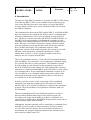
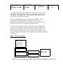
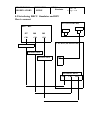
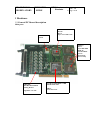
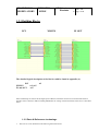
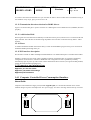
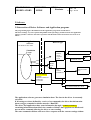
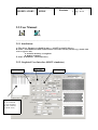
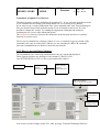
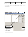
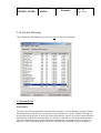
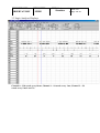
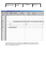
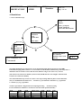
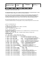
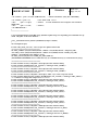
STOCKHOLM
OBSERVATORY
HERSCHEL
SPIRE
DRCU Instrument
Simulator
Date : 2003-11-26
Issue : 1.0
P Page : 1 / 36
DRCU Instrument Simulator
Hardware
Software
User Manual
ver 1.5
Stockholm Observatory
H-G Florén
[email protected]
Göran Olofsson
[email protected]
ICU Polska sp. z o.o.
Świętojańska 75/4
81-389 Gdynia
Tel: +48 58 621 7920
Fax: +48 58 661 6726
e-mail: [email protected]
Source code and this document could be downloaded from
http://www.astro.su.se/~floren/download_sim.htm
STOCKHOLM
OBSERVATORY
HERSCHEL
SPIRE
DRCU Instrument
Simulator
Table of contents
0.0 Introduction
0.1 Product Tree
0.2 How to Connect
1 .Hardware
1.1 General PCI board description
1.2.1Parts & References to drawings
1.2.3 Fast channels receivers (HSII)
1.2.4 Slow channels’ transmitters
1.2.5 Internal registers address decoder
1.2.6 Interrupt mask
1.2.7 Clock 20 MHz dividers
1.2.8 500 us interrupt
1.2.9 FIFO control signal generation
1.2.10 FIFO busy signals generator
1.2.11 Fast channel selection signal (H4)
1.2.12 Transmission direction selection for RS485 drivers
bus Hold description
1.2.13 Add-on bus Hold description
1.2.14 Reset
1.2.15 PCI interface description
1.3
Connectors and pin functions
1.4.1 Computer Controlled Power Consumption Simulator
1.4.2 Example
2.Software
2.1 Interaction of Driver - and Application-software
2.2 Driver software.
2.3 Application software
2.4 Transmitter:
2.5 User Manual
2.5.1 Installation:
2.5.2 Graphical User Interface (DRCU simulator)
2.5.3 How to use and Store Settings.
2.5.4 Receiver IF
2.5.5Test Examples(Current implementation)
2.6.1 Log Files
2.6.2 LogFileReader
2.7Commanding The Power consumption Load Simulator
2.8.Network connection
2.9.1How to modify application software
2.9.2 How to define new simulation functions
2.9.3 Current Implementation
/How To Define New Actions Upon Incoming Request
2.10 Trouble Shooting
3 Testing
3.1 System tests
3.2 Logic Analyser Displays
Date : 2003-11-26
Issue : 1.0
P Page : 2 / 36
STOCKHOLM
OBSERVATORY
HERSCHEL
SPIRE
4 Simulations
4.1 SCU simulation loops
5 Examples (How to)
6 Appendix
A1
A2
A3
A4
A5
A6
A7
A8
A9
A10
A11
A12
A13
A14
A15
A16
A17
A18
A19
A20
A21
A29
Building Blocks
PCI/IF
XILINX overview
XILINX Transmit Main
XILINX Transmitter FastChannel
Transmitter IRQ Mask
Transmitter Phase
Transmitter Slow Channel Input P
Transmitter Slow ChannelInput
Transmitter Slow Channel Output
Receiver Main
Receiver Fast Channel
Receiver IRQ Mask
Receiver Phase
Receiver Slow Channel Input
Receiver Slow Channel Output
In and Out drawings
Cables Pin Assignment
Cable I/F
Terminators
RS 422 definition ADM 485
Power Consumption Simulator circuit layout
DRCU Instrument
Simulator
Date : 2003-11-26
Issue : 1.0
P Page : 3 / 36
STOCKHOLM
OBSERVATORY
HERSCHEL
SPIRE
DRCU Instrument
Simulator
Date : 2003-11-26
Issue : 1.0
P Page : 4 / 36
0. Introduction.
The purpose of the DRCU simulator is to replace the DRCU+FPU during
tests when the DRCU+FPU are not available. In particular this is the
case for the Herschel Oavionics¹ tests where it is part of the SPIRE
Avionics Model (AVM), but it is also intended for DPU I/F tests and
the OBS development.
The communication between the DPU and the DRCU, as defined in RD1,
does not conform to any standard and for this reason a communication
I/F board (called Hermes¹) have been developed, to mate to the PCI
bus . The driver software runs under MS WinNT and MS Win2000. As
the DRCU will react promptly to commands (by returning an echo
including 2 bits acknowledgement¹) the DRCU simulator must do the
same. This type of real-time performance requires a kernel¹ separate
form the operating system, and for this reason, the Hermes software
driver includes this feature. The simulation software, called
application¹ software feeds continuously the driver memory area with
HK data, status information, simulated signal data etc. In this
manner there is always a fresh¹ response available in the driver
memory area for a request from the DPU.
The 32 bit command word has a 12 bit wide CID (command identifier)
field and MSB=1 the command is a read (called get) command, asking
for a specific HK value or status parameter. The simulator responds
by first sending an echo (identical to the command except with a 2
bit ACK field instead of the channel_No field) and then the requested
information. A command with MSB=0 in the CID field is a write (called
set) command and as for get command the immediate response is an
echo. In addition, a set command usually means some setting of the
(simulated) instrument and the application software will react to it
in a similar way as the real instrument.
In order to get an overview of the current state of the (simulated)
instrument, one form that contains all the CID entries for each of
the three (DCU, SCU and MCU) channels is coupled to the simulation
program. The forms(windows) are updated in accordance with new
set commands..
The most demanding task for the simulation program is to deliver
detector and mechanism data frames at the required speed, and
according to the requirements (RD2) it produces a simulation of a
celestial source modulated by the BSM in the photometer mode and an
interferogram in phase with the SMEC.
Although the simulator normally will be controlled by commands from
the DPU, it is also possible to insert parameters directly by means
of a GUI. This tool also displays the current status and activity of
the simulator. By using the network connection the simulator can be
used remotely with the same GUI.
STOCKHOLM
OBSERVATORY
HERSCHEL
SPIRE
DRCU Instrument
Simulator
Date : 2003-11-26
Issue : 1.0
P Page : 5 / 36
All information transmitted by the DRCU simulator is saved to disk in
datalog files. The growth rate of these obviously depends on the mode
of operation, but the disk space will in normal running modes allow
several days of continuous operation.
In order to simulate the power consumption of the DRCU+FPU, a
separate power drain unit has been constructed. This unit is
controlled by the simulator PC via a RS232 connection and allows e.g.
simulation of the power-up sequence and failure modes.
In order to test and run the Hermes communication (including cables
that are part of the DRCU simulator package), a DPU simulator¹ has
been developed that also consists of a PC with a Hermes board. This
Hermes board is configured in receiver mode for the fast channels and
GUI of the application program allows sending of commands, monitoring
of signals etc.
DRCU / DPU unit interface
DRCU unit
Standard PC
Application Win
2000/NT GUI
Driver (low level
logic )
Hermes
PCI Card
3xSlow Channels
Bidirect. 332 KHz
DPU unit
3xFast Channels
one direct 1 Mbit/s
Electrical I/F format complies with the DRCU/DPU unit SPIRE-SAP_PRJ-001324 (2) description
STOCKHOLM
OBSERVATORY
HERSCHEL
SPIRE
DRCU Instrument
Simulator
Date : 2003-11-26
Issue : 1.0
P Page : 6 / 36
0.1 DRCU Simulator Product Tree
HS-DSIM
HS-DSIMx-100
HS-DSIMx-200
HS-DSIMx-300
HS-DSIMx-400
HS-DSIMx-500
HS-DSIMx-600
HS-DSIMx-700
HS-DSIMx-700-01
HS-DSIMx-700-02
HS-DSIMx-700-03
HS-DSIMx-700-04
HS-DSIMx-800
HS-DSIMx-900
DRCU Simulator
CPU Box
CPU Power Cable
Keyboard
Mouse
Monitor
MonitorPower Cable
DPU I/F Cables
Cable I/F to PCI card (mounted) Hermes Interface
Cable CH1
Cable CH2
Cable CH3
Power Consumption Simulator
PCS Cable
HS_DSIMx 700 cables are symmetric. Red or green is arbitrary.
STOCKHOLM
OBSERVATORY
HERSCHEL
SPIRE
DRCU Instrument
Simulator
Date : 2003-11-26
Issue : 1.0
P Page : 7 / 36
0.2 Interfacing DRCU Simulator and DPU
How to connect
PCS (HS-DSIMx-800)
DPU –Box
RS 232
Load
J07
J08
CH1
J09
CH2
CH3
CPU-BOX (HS-DSIMx-100)
HS-DSIMx-700-02
HS-DSIMx-700-03
HS-DSIMx-700-04
Com
1 or 2
HS-DSIMx-700-01
CH1
CH2
CH3
STOCKHOLM
OBSERVATORY
HERSCHEL
SPIRE
DRCU Instrument
Simulator
Date : 2003-11-26
Issue : 1.0
P Page : 8 / 36
1 Hardware
1.1 General PCI board description
Main parts
XILINX SPARTAN
XCS30
FPGA
http://www.xilinx.com/
20 MHz
Clock
Memory
SN74
ACT7882-20FN
2048*18
Clocked FIFO
[Texas
Instrument
www.ti.com]
ADM 485
EIA RS-485 Standard
Analog Devices
Appendix A17-A25
PCI MATCHMAKER CARD
S59200 0106 A027
AMCC
www.amcc.com/
STOCKHOLM
OBSERVATORY
HERSCHEL
SPIRE
DRCU Instrument
Simulator
Date : 2003-11-26
Issue : 1.0
P Page : 9 / 36
1.2.1 Building Blocks
PCI
XILINX
IN OUT
The detailed logical description of the blocks could be found in appendix (A)
PCI
XILINX
A3-A15
IN and OUT
A17
A2
Xilinx XCS30TQ144 contains all the digital parts of Hermes transmitter and receiver boards besides the PCI
interface which is based on AMCC S5920Q Matchmaker IC. Design of both transmitter and receiver is described
below.
1.2.2 Parts & References to drawings
1.
The receiver can be divided into the following functional blocks:
STOCKHOLM
OBSERVATORY
HERSCHEL
SPIRE
DRCU Instrument
Simulator
Date : 2003-11-26
Issue : 1.0
P Page : 10 / 36
A detailed logic layout could be found in the Appendix. (1-16)-use the search function in the appendix section
to locate the ( )- parts and if needed the zoom function if needed.
•
•
•
•
•
•
•
•
•
•
•
•
•
fast channels receivers
( H1 .. H3 )
slow channels transmitters ( T1 .. T3 )
slow channels receivers ( R1 .. R3 )
internal registers address decoder ( L8, I56 )
interrupt mask register ( U1, I25, I26, I57 )
20 MHz clock dividers
500 us interrupt generator ( U3, I150, I151 )
FIFO control signals generation ( I88, I89, I90 )
FIFO busy signals generation ( I142, I143, I144 )
fast channel selection circuit ( H4 )
RS485 direction definition ( I83 )
Add-On bus Hold ( I75 )
Reset
An external 20 MHz creates a basic clock for all receiver parts. Transmission CLKOUT 312,5 kHz, LED 1,5 Hz
are generated by dividing 20 MHz. It is distributed by one of BUFGP lines to guarantee small delays. PTADR,
DXFR and 1 MHz CLKIN from transmitter are also distributed using BUFGP lines. PTWR, CLKOUT, RD1 and
CLKIN are distributed using secondary BUFGS buffers.
1.2.3 Fast channels receivers (HSII)
Serial channel input data are converted to a word in L14 module. Consecutive word bits are registered on rising
edge of 1 MHz clock while frame FR is active. Parallel data are latched in L16 by a rising edge of 20MHz clock
when LATCH_EN is active. LATCH_EN is generated by I162, I163, I550 and is active for half of CLKH period
after FR goes low. The word received is written to FIFO by signals generated in I471, I487, I488 and I490. Write
begins when both LATCH_FULL and channel selection Q are high. WRITE signal is generated and fed to I488. If
Add-On bus is free ( DXFR and PTATN are high) WAIT is generated forcing third state on S5920 outputs. On the
next 20MHz cykle FIFO write enable (WEN) is generated. The next 20 MHZ clock generates CLR that resets the
circuit. Simultaneously WAIT opens L15 buffer and the data received are presented on P[15:0] bus. Fast channel
receiver can generate three interrupts IRQ1, IRQ2, IRQ3. IRQ1 is generated on FR transition from high to low,
IRQ2 on break between frames longer than 1 CLKH period, IRQ3 on FIFO’s AF ( almost full ) transistion from 1
to 0. The interrupts are cleared by CLR_IRQ generated by I132 from DXFR, PTWR, EN (Add-On write to a
given fast channel).
1.2.4 Slow channels’ transmitters
After 32 bit word is written to a slow channel CLK_EN is generated and the data are latched in L16.
Simultaneously START is generated starting 32 CLKL periods long FR frame. I163 register synchronises CLKL
to START and additionally generates RDY, that together with FR defines the moment when data are written
(LOAD) to shift registers module L17. L10 modul generates CLR after 32 CLKL periods are counted. CLR clears
FR. The word written to L17 is transmitted through SER serial output starting from MSB. When FR goes low I
interrupt is generated. This interrupt is cleared by the appropriate channel read operation (CLR_IRQ from I160 ).
Change from 0 to 1 on S serial input results in FR changing from 0 to 1 and starts L11 counter counting 32 CLKL
cycles. Simultaneously CLKL pulses write word bits to L10 shift register. The word is then presented on
DO[31:0] bus. After 32 CLKL pulses I147 register resets (FR=0). Falling FR edge is detected in I141, I142
registers and CLK_EN is generated. CLK_EN enables word write to L12. Rising CLK_EN produces LATCH_EN
STOCKHOLM
OBSERVATORY
HERSCHEL
SPIRE
DRCU Instrument
Simulator
Date : 2003-11-26
Issue : 1.0
P Page : 11 / 36
and I interrupt. I interrupt is cleared by write to appropriate slow channel (CLR_IRQ from I144). The word
received is presented on P[31:0] bus when the appropriate channel is selected (EN).
1.2.5 Internal registers address decoder
Address from Add-On bus is transmitted to BUSIN[31:0] and latched in L8 module by rising edge of PTADR. It
is then transmitted over A[3:0] to I56 address decoder.
1.2.6 Interrupt mask
Interrupts generated by the modules are connected to internal bus DQ[15:0] transmitting them to U1. Module U1
contains 16 registers (L10) where a present interrupt mask is stored. There are also 16 AND gates masking the
interrupts for which a mask bit is equal to 0. The result is presented on O[15:0]. The interrupt mask can be
changed by writing a new value to IRQ_MASK address. After reset the mask has a value of 0x00. O[15:0] bus is
buffered by L4 buffer. L4 is opened when read of interrupt vector occured. All the interrupt lines are also added
by I26, I57 and I25 to create ADDINT.
1.2.7 Clock 20 MHz dividers
20 MHz external clock (generated by quartz oscillator installed on Hermes) is divided by 64 with a duty factor of
50% (L7) to produce 312,5 kHz clock. This signal is then buffered by BUFGS (for fast propagation in Xilinx) and
creates receivers CLKOUT (being the transmission clock for slow channels). CLKOUT is divided by 200000 in
L2 with a duty factor of 50% and provides approx. 1.5 Hz signal to control on board LED.
1.2.8 500 us interrupt
CLKIN (1MHz fast channel transmission clock coming from transmitter) is divided by 500 in U3 with a duty
factor of 1/500. It is then synchronised by I151 and fed to line 15 of DO[15:0] bus. 500 us interrupt is cleared by
Add-On write to INT_TICK address.
1.2.9 FIFO control signals generation
FIFOs’ read signals REN1, REN2, REN3 are generated by I88, I89, I90 when Add-On read from H1, H2 or H3
address occurs.
1.2.10 FIFO busy signals generation
When a 16 bit value is read from FIFO there are OR1, OR2 or OR3 signals presented on Add-On bits 16, 17 and
18 respectively. They are used to confirm that the value read is valid.
1.2.11 Fast channel selection signal (H4)
STOCKHOLM
OBSERVATORY
HERSCHEL
SPIRE
DRCU Instrument
Simulator
Date : 2003-11-26
Issue : 1.0
P Page : 12 / 36
It is used to select three fast channels in a cycle one after the other to assure conflict free received data writing to
one of FIFOs. Every of Q1, Q2, Q3 is active for 3 uS.
1.2.12 Transmission direction selection for RS485 drivers
Logical 1 is fed from I85 gate to pin P75 of Xilinx. It is defining the level on RS485 drivers (ADM485) direction
pin [M1].
1.2.13 Add-On bus Hold
WAIT signals from fast channels are added by I75 and fed to Xilinx pin P4, which in turn is connected to WAIT
input of S5920. Active WAIT sets S5920 in high impedance state. The bus can be then used by Xilinx – FIFO
transfers.
1.2.14 Reset
A standard STARTUP module from Xilinx library is used. S5920 SYSRES (program reset) pin is connected to
STARTUP GSR input through P116 pin.
1.2.15 PCI interface description
PCI interface is based on AMCC S5920Q PCI Matchmaker IC. Its detailed description is available from AMCC.
S5920Q is working in active mode. It has a standard connection with the PCI bus. Its operation is defined by
configuration record written to 24C02 I2C EEPROM. This configuration record is uploaded by S5920Q
automatically upon its power up. This record contains information about resources (I/O region and IRQ number)
used by the board and the board descriptor.
1.3 Connectors and pin functions
Appendix p17 Pin Out Cables
Appendix -p18 Cables I/F drawings
Appendix p19 Terminators
1.4.1 Computer Controlled Power Consumption Simulator
Users Guide
Computer Controlled Power Supply Load (CCPSL Appendix p29) is a variable PS load that can be used to
simulate changes in power consumption for 28 V power supply. It works in the range from 0.84 W up to 120 W.
Fuse F 6.3A
Load
LED
RS232
STOCKHOLM
OBSERVATORY
HERSCHEL
SPIRE
DRCU Instrument
Simulator
Date : 2003-11-26
Issue : 1.0
P Page : 13 / 36
CCPSL front case
The front of CCPSL case is shown above. There are two DEMA9 connectors marked „Load” (DEMA9P) and
“RS232” (DEMA9S), fuse holder and LED on the it.
The power supply output should be connected to “Load” input with positive voltage connected to pins 2 and 7 and
ground connected to pins 4 and 8. There is fast 6.3A fuse installed in serial with “Load” input to protect the load
against overcurrent in case of failure.
CCPSL acts as a regulated current load. The current value is set by a controlling computer through RS232 (serial)
interface. The interface is optoisolated and requires small amount of power from the computer. The supply voltage
is taken from RTS line which must be active for the interface to operate correctly (+12V). It is therefore necessary
to set flow control for the designated serial port to RTS/CTS.
Transmission parameters are set to 2400 bauds, 8 data bits, no parity control and one stop bit (2400, 8, N, 1).
All the internal CCPSL electronics is supplied from “Load” input. Therefore there is always certain minimal
current taken from the PS under test. This current is equal to 30 mA.
To set a given current value the user has to send two bytes to CCPSL:
X – current value
0x21 (ASCII code of “!”)
The maximum current value tha can be set is adjusted to 4 250 mA. If we add 4 250 mA and a constant supplying
current of 30 mA we will have the maximum current that can be set equal to 4 280 mA which gives a maximum
power of 119.84 W for voltage of 28V.
A single bit weight is equal to 16.60 mA (0.465 W). The minimum current of 30 mA gives a minimum load of
0.84 W.
1.4.2 Example:
To set power to 45 W user has to send:
(45 W – 0.84 W)/0.465 W = 95 (0x5F)
User can also read the real current and voltage values by sending 0x3F (ASCII “?”) to CCPSL. CCPSL will
answer with two bytes representing voltage and current
X, Y
To calculate voltage and current the following equations should be used:
U [V] = X * 0.129 + 0.45
I[A] = Y / 60 + 0.03
Example:
The answer 0xDA 0x5C means 28.6 V and 1.56 A.
The LED mounted above RS232 connector signals current consumption ranges
green – I =0
orange – 0 < I < 3 A
red – I > 3 A
RS232 cable is “one to one” (i.e. pin 1 connected to pin 1 and so on) DEMA9P to DEMA9S. However only four
lines (TxD, RxD, RTS and GND) are used.
STOCKHOLM
OBSERVATORY
HERSCHEL
SPIRE
DRCU Instrument
Simulator
Date : 2003-11-26
Issue : 1.0
P Page : 14 / 36
2 Software
2.1Interaction of Driver Software and Application program.
The programming logic is divided between the application programme and the driver.
The driver manage very fast response independent of the operating system drawback. The application
software provides a GUI for interactive operation. The division of tasks between the two levels are as
follows
Application
software
Driver Logic
OS Windows NT /2000
Simulation
Loops
Get
Buffers
32-bit
response
word
Borland C++ builder
32-bit GET ECHO inc ACK
GET
Command word
Status
Buffer
ACK
Set
Buffers
DataBlocks
Fast Channel
Block transfer
0-2
Common memory
1.Length
2.Number Of Blocks
3.TimeGap
4. RunCID
SET
32-bit SET ECHO inc. ACK
The application software generates simulation data. The data in the driver is constantly
refreshed
If all settings are done (defined by a series of set commands) the driver has information
about a trigger command to initiate transfer-“RunCID”.
The driver and application share some information through a common memory
containing information about block size, number of blocks, time gap between blocks and
start transfer command allowing the driver to start sending
The start command will then activate a driver response with the current settings without
STOCKHOLM
OBSERVATORY
HERSCHEL
SPIRE
DRCU Instrument
Simulator
Date : 2003-11-26
Issue : 1.0
P Page : 15 / 36
having to enter the application software New blocks are shifted to the driver from the
simulation loop as the transfer progresses.
2.2 Driver software.
Development tools: Visual c++ (Microsoft)
http://www.microsoft.com
Driver Studio 2.0 and SoftICE DriverStudi(Compuware Corporation)
(http://www.microway.com.au/catalog/listcpp_addons.htm )
--------------------------------Driver start-up
The board driver (hermes.sys) is loaded during Windows NT startup. This driver is uploading the Xilinx
definition file (defining its internal structure) using S5920Q mailbox MD0 and MD1 bits.
After the Xilinx definition file is uploaded, S5920Q communicates with registers created in Xilinx structure
using 32 bit data DQ bus and control signals ADCLK, DXFR#, PTATN#, PTADR#, PTWR and IRQ#. The
communication between S5920Q and Xilinx XCS30 does not use any wait states.
-----------------------------------------------------------------------------------------------------
2.3 Application software
Development tool: Borland C++ Builder.5.0
The Application software is referred to as transmitter and receiver.
The transmitter is the simulator (DRCU) and the receiver (DPU) making it possible to test
setup.
In the application programme (transmitter) the simulation functions will be implemented
STOCKHOLM
OBSERVATORY
DRCU Instrument
Simulator
HERSCHEL
SPIRE
Date : 2003-11-26
Issue : 1.0
P Page : 16 / 36
2.4 Transmitter:
Main units in application software(detailed listing in appendix)
Form1
Main Window
BitFunc
Unit containing some simple bit conversion function
Driver
Open the Driver
Function
Place To Define New Simulation Functions (Data for fast channels will be generated here)
LogFiles
Log File storage
Request
Incoming requests that the simulator should react on
Settings
of transfer specifics
Transmit
Main wrapper file for application execution
Form2 & Unit2 Database handeling
UpdateF Transfer to Driver Buffer of Fast Channel response data
DeviceIoControl(Drv, CHANGE_FAST, pb, len, NULL, 0, &u, NULL); // send it !
UpdateS Transfer to Driver of Slow Channel Response data.
DeviceIoControl(Form1->Drv->hDrv, WRITE_SLOW, &LS_Par, sizeof(LS_Par), NULL, 0, &i, NULL);//send
it !
Only Demo and test modes will not be used (currently not active)
---------UpDataDisplay A Thread to display detector data (will not be used )
Form3 & Unit3 Display of Detector readout.
The project also contains a file Common.h that serve as a link between application and driver.
Common.h Link between application and driver.
#ifndef __Common__
#define __Common__
#include "Typedef.h"
#define HermesVer "Hermes 3.3"
#define LOAD_XILINX
#define RESET_XILINX
#define CREATE_HOOK
#define READ_SLOW
#define WRITE_SLOW
#define CHANGE_FAST
#define FLUSH_FIFO
#define READ_LOG
0x00222000
0x00222004
0x00222008
0x0022200C
0x00222010
0x00222014
0x00222018
0x0022201C
// CCAA TIII IIII IIII PPPP PPPP PPPP PPPP --- drv -> appl
// GGSS xIII IIII IIII PPPP PPPP PPPP PPPP --- appl -> drv
// CC - channel number
// SS - acknowledge bits for SET command
Format Definition
Note that the two
First bits GG are
used internally to
DefineAck bits
For get commands
STOCKHOLM
OBSERVATORY
HERSCHEL
SPIRE
DRCU Instrument
Simulator
Date : 2003-11-26
Issue : 1.0
P Page : 17 / 36
// GG - acknowledge bits for GET command
// PPPP PPPP PPPP PPPP - parameter
#define GET_MASK
0xC0000000
#define SET_MASK
0x30000000
#define PAR_MASK
0x0000FFFF
#define CHN_ID(p) ((UCHAR)(((p)&GET_MASK) >> 30))
#define ACK_ID(p) ((UCHAR)(((p)&SET_MASK) >> 28))
#define CMD_ID(p) ((USHORT)(((p)&0x0FFF0000) >> 16))
#define CMD_NR(p)
((USHORT)(((p)&0x07FF0000) >> 16))
#define CMD_SG(p) ((UCHAR)(((p)&0x08000000) ? 0x01 : 0x00))
#define PAR_ID(p) ((USHORT)((p)&PAR_MASK))
#define CH
3
// number of channels
#define MIN_LEN 5
// min frame length
#define MAX_FN
16
// max number of functions for one channel
#define MAX_DAT
1023
of words in single block
#define MAX_LS
2048
of SET/GET parameters
#define MAX_REQ 200
// max size queue of requests
#define MAX_BLK 200
// max size queue of blocks
Range definitions
// max number
// max number
Block
Definition
typedef struct _BLOCK
{
USHORT
Length;
// number of data words
USHORT
Data[MAX_DAT];
} BLOCK;
// Frame ID - stored in Data[0]
// Time words and CRC stored in Data table (various positions)
typedef struct _FAST_O
{
USHORT Channel;
USHORT Loop;
USHORT
BlkNum;
USHORT RunCid;
BLOCK
// single block format
// one extra word for CRC
// application --> driver
FAST OUT
Definition
// which channel
// loop mode active
// number of blocks
+ Block struct
// command "start block transfer"
Block;
// block
} FAST_O;
typedef struct _FAST_I
// application <-- driver
{
USHORT Channel;
// which channel
BLOCK
Block;
// block
} FAST_I;
typedef struct _LS_PAR
// parameters for slow channels
{
ULONG Data[CH][MAX_LS]; // mixed ACKs/PARAM words
} LS_PAR;
typedef struct _LS_ONE
{
USHORT
// GET CMD for channels
Channel;
// which channel
STOCKHOLM
OBSERVATORY
HERSCHEL
SPIRE
USHORT Idx;
ULONG Param;
DRCU Instrument
Simulator
Date : 2003-11-26
Issue : 1.0
P Page : 18 / 36
// index of ACK/PARAM word
// mixed ACK/PARAM word to change
} LS_ONE;
typedef struct _CHANGE
{
ULONG
// single transaction for slow channel
In;
// incomming word
Out;
// outgoing word
Stamp;
ULONG
LONGLONG
// time stamp
} CHANGE;
#endif
// __Common__
STOCKHOLM
OBSERVATORY
HERSCHEL
SPIRE
DRCU Instrument
Simulator
Date : 2003-11-26
Issue : 1.0
P Page : 19 / 36
2.5 User Manual
Hermes.sys
Hermes.reg
-----------------------------------------------------------------------------------
2.5.1 Installation:
A. The driver Hermes.sys should be put c:\ winNT\system32 \drivers
B. Folder TransmittPhase3 2002-12-09 contains source files and the (Hermes.reg i double click
on it to registrer file).
C: Create a directory “C:\LogFiles”
D. Reboot computer
E. Start Transmitter (Start Receiver)
2.5.2 Graphical User Interface (DRCU simulator)
BlockLength
Display Window
S=set command
G=get command
R=run command
(transfer starts)
RUN CMD
TimeGap[ms]
STOCKHOLM
OBSERVATORY
HERSCHEL
SPIRE
DRCU Instrument
Simulator
Date : 2003-11-26
Issue : 1.0
P Page : 20 / 36
Transmitter Graphical User Interface
The different modes could be defined in the graphical I/F. If you select the predefined modes
in the comboboxes the settings will change block size etc for that specific channel.
If you want to test a certain combination enter values manually and click TransferSettings to
file.(you should always finish with this update if you do changes in the boxes. It is also
possible to change the “modes” by sending the appropriate command and parameter
combination (see receiver side instruction below)
The sim function selector references the definitions in the function unit (how to redefine
function see section xxxx)
The received command box will show if there is a set =s command or get=g comand. If the
command is the same as in the RUN CID box it is also considered a RUN =R command.
(the start command known to the driver that will start transfer.
2.5.3 How to use and Store Settings.
The set parameters are send to the simulator there they are stored and displayed.
Three separate windows are defined for each channel. CH0,CH1,CH2
(use SETTINGS|CH0 orCH1 or CH2 to store and modify values)
SET CMD
Switch
defines
Runtime var
Show settings
In GUI
CH0,CH1,CH2
Make GUI changes
Active (transfer to run-time
var)
Get settings
To GUI from
file
Store
Settings to file
You are free to make changes in the GUI. After pressing “TransferGUIchangesToDriver”
STOCKHOLM
OBSERVATORY
HERSCHEL
SPIRE
DRCU Instrument
Simulator
Date : 2003-11-26
Issue : 1.0
P Page : 21 / 36
The settings become active in the simulation loop. Note Settings files are generated separately
for each channel.The settings are not automatically stored you have to do that by pressing
StoreCurrentSettings->
2.5.4“Receiver” I/F (DPU) software used for testing the “simulator side”
Commanding the simulator:Channel To Send On 0-2
Command Number
Make sure the same cheksum
is selected on both sides
1
2
3
4
Select channel 0,1,2
Enter command number
Enter parameter value
Press Send Now
Hex or
Decimal
Display
Parameter
STOCKHOLM
OBSERVATORY
HERSCHEL
SPIRE
DRCU Instrument
Simulator
Date : 2003-11-26
Issue : 1.0
P Page : 22 / 36
2.6.1 Log Files
Logfiles are stored in directory c:\LogFiles Remenber to clear that directory if disk-space become crucial.
In Hermes phase 3 software the driver and „Transmit.exe” were modified. All the data received or sent by
transmitter are written to files.
If Transmitter program is started it creates in the (c:\LogFiles) four files with the following names:
„HHMMSSs.log”
„HHMMSSf0.log”
„HHMMSSf1.log”
„HHMMSSf2.log”
- a common file for all slow channels,
- file for channel 0,
- file for channel 1,
- file for channel 2.
where HH is the current hour, MM minutes, SS seconds.
1. Slow channels
The following changes were implemented in the driver and transmitter application to log the data:
- added „DeviceIoControl” function named READ_LOG,
- write to a file was added to receiving thread („Request”).
READ_LOG function operates similarly to READ_SLOW function that was already used in
previous versions of software. There is however a small difference between the two functions.
In READ_SLOW a queue of single words was read. In READ_LOG a queue of CHANGE
structures defined in „common.h” is read. Every structure consisits of the following fields
:
- ULONG In
- a request received from „Receiver.exe”
- ULONG Out
- an answer sent to „Receiver.exe”
- LONGLONG Stamp
- „time stamp” (FILETIME structure)
All the structures read are written one after the other to „HHMMSSs.log” file.
The size of file is equal to:
Size = number of words received * sizeof(CHANGE) = number of words received * 16
2. Fast channels
Blocks of data to be sent are additionally stored in COPY_F structure (defined in „UpdateF.h”)
in every thread preparing data for fast channels („UpdateF”). The COPY_F structure is
complemented with time stamp. The structure consists of:
- LONGLONG Stamp
- FAST_O Data
- time stamp (FILETIME structure)
- data block (variable length!)
CHANGE_FAST function was modified. Now the driver informs the application that a given
block of data was used i.e. transmitted through a fast channel. If it happens, its copy is written
to an appropriate „HHMMSSf?.log” file.
STOCKHOLM
OBSERVATORY
HERSCHEL
SPIRE
DRCU Instrument
Simulator
Date : 2003-11-26
Issue : 1.0
P Page : 23 / 36
For every transmission the length of a file is increased per:
:
Size = number_of_blocks_sent * (number_of_data_in_the_block + 11) * 2
Remarks
You may use FileTimeToSystemTime (Windows SDK) function to use time stamp.
After „LOG” checkbox is pressed present *.log files are closed and new ones are created.
Data are written to files by unsynchronised threads and the data may be corrupted if you
use the „LOG” checkbox during the active fast channel transmission.
2.6.2 Log file Reader
A preliminary file reader is available to view contents Developed in C++ builder.
Load either
All blocks
Or a certain
number of
blocks from
BEOF
2.7Commanding The Power consumption Load Simulator
We have constructed simple commanding I/F based on C++ builder and Asynch professional
(www.turbopower.com) plug in software is used for the serial communication. It could be integrated with the
application programme.
2.8.Network connection
STOCKHOLM
OBSERVATORY
HERSCHEL
SPIRE
DRCU Instrument
Simulator
Date : 2003-11-26
Issue : 1.0
P Page : 24 / 36
We have tested to operate the simulator remotely. For that purpose we used Remote Admin
(see http://www.famatech.com/). Other commercially available software should also work. In standard
networks.
2.9.1How to modify application software
Open C++ Builder project file
Open the Function Unit
Locate
void FuncInit()
void FuncInit()
{
UCHAR i, j;
randomize();
for(i=0; i<CH; i++)
for(j=0; j<MAX_FN; j++)
{
Channel No
Form1->Set.pFnHS[i][j] = NULL;
Func No
Form1->Set.pFnLS[i][j] = NULL;
}
// Assign functions
Form1->Set.pFnHS[0][0] = D0;
Form1->Set.pFnHS[0][1] = D1;
Form1->Set.pFnHS[0][2] = Time_F2;
…..
Function Definition
Selected in
ComboBox
SimFunction
(GUI)
Form1->Set.pFnHS[1][0] = T0;
Form1->Set.pFnHS[1][1] = Time_F1;
…..
Form1->Set.pFnHS[2][0] = Specctro_Array_F;
Form1->Set.pFnHS[2][1] = Time_F2;
Form1->Set.pFnHS[2][2] = Crazy_F;
……
}
2.9.2 How to define new simulation functions
void D0(BLOCK *pb)
{
USHORT *pd = &pb->Data[0];
USHORT n = pb->Length - MIN_LEN; // Length, Frame ID, TmrTag1, TmrTag2, CRC
SYSTEMTIME tm;
GetSystemTime(&tm);
int index = Form1->ComboBox3->ItemIndex;
*pd++ =FrameId(index);
int i=0;
while(n--) *pd++ = (int)(1000*(1+sin(0.002*M_PI*Form1->mirror_pos)));
*pd++ = tm.wSecond;
// TmrTag1
*pd = tm.wMilliseconds; // TmrTag2
Variable from separate Timer Thread
Event Changing the position (t )
STOCKHOLM
OBSERVATORY
HERSCHEL
SPIRE
DRCU Instrument
Simulator
Date : 2003-11-26
Issue : 1.0
P Page : 25 / 36
}
2.9.3 Current Implementation
/How To Define New Actions Upon Incoming Requests
All set commands are branched in huge switch sentence, defining all set commands
individually.
First the three channels are separated
switch(Ch)
{case 0: {
//// Form1->GET_[2][ch][CID]= StrToInt(A_1025) Updateing of Ack commands
switch(Cmd)
{case 3 : { Form1->start_time_ms =timeGetTime();Form1->Edit3->Text="Reset_Timer"; }break;
resoultioin
Set command number is selected, graphical GUI channel 1 and the driver buffers are updated
case 1024: { Form6->C0_1024->Text=IntToStr(Par);Form1->GET_[0][0][1024]=Par;}break;
case 1025: { Form6->C0_1025->Text=IntToStr(Par);Form1->GET_[0][0][1025]=Par;}break;
case 1026: { Form6->C0_1026->Text=IntToStr(Par);Form1->GET_[0][0][1026]=Par;}break;
case 1027: { Form6->C0_1027->Text=IntToStr(Par);Form1->GET_[0][0][1027]=Par;}break;
case 1028: { Form6->C0_1028->Text=IntToStr(Par);Form1->GET_[0][0][1028]=Par;}break;
case 1029: { Form6->C0_1029->Text=IntToStr(Par);Form1->GET_[0][0]
[1029]=Par;SET_VSSp(1,24,Par);}break; //VSS1
Sometimes additional functions are called
case 1030: { Form6->C0_1030->Text=IntToStr(Par);Form1->GET_[0][0]
[1030]=Par;SET_VSSp(25,24,Par);}break;
case 1031: { Form6->C0_1031->Text=IntToStr(Par);Form1->GET_[0][0]
[1031]=Par;SET_VSSp(49,24,Par);}break;
case 1032: { Form6->C0_1032->Text=IntToStr(Par);Form1->GET_[0][0]
[1032]=Par;SET_VSSp(73,24,Par);}break;
case 1033: { Form6->C0_1033->Text=IntToStr(Par);Form1->GET_[0][0]
[1033]=Par;SET_VSSp(97,24,Par);}break;
case 1034: { Form6->C0_1034->Text=IntToStr(Par);Form1->GET_[0][0]
[1034]=Par;SET_VSSp(121,24,Par);}break;
case 1035: { Form6->C0_1035->Text=IntToStr(Par);Form1->GET_[0][0]
[1035]=Par;SET_VSSp(145,24,Par);}break;
case 1036: { Form6->C0_1036->Text=IntToStr(Par);Form1->GET_[0][0]
[1036]=Par;SET_VSSp(169,24,Par);}break;
case 1037: { Form6->C0_1037->Text=IntToStr(Par);Form1->GET_[0][0]
[1037]=Par;SET_VSSp(193,24,Par);}break;
case 1038: { Form6->C0_1038->Text=IntToStr(Par);Form1->GET_[0][0]
[1038]=Par;SET_VSSp(217,24,Par);}break;
case 1039: { Form6->C0_1039->Text=IntToStr(Par);Form1->GET_[0][0]
[1039]=Par;SET_VSSp(262,24,Par);}break;
case 1040: { Form6->C0_1040->Text=IntToStr(Par);Form1->GET_[0][0]
[1040]=Par;SET_VSSp(241,21,Par);}break; //VSS12
case 1041: { Form6->C0_1041->Text=IntToStr(Par);Form1->GET_[0][0][1041]=Par;}break;
This is the section to add new functions function calls, triggered by set commands
”Request Unit”
//1 ms
STOCKHOLM
OBSERVATORY
HERSCHEL
SPIRE
DRCU Instrument
Simulator
Date : 2003-11-26
Issue : 1.0
P Page : 26 / 36
2.10 Trouble Shooting
Check Windows Task Manager So that only one transmit.exe is running
3.1 System Tests
Performance
The processor load on transmitter side depends on number of active channels, lengths of blocks
and breaks between the blocks. For the most critical situation i.e. all the channels working, no
breaks between the blocks (if the break between the blocks’ starts is set to time smaller than the
transmission of the block time then there is a break of 2 stop bits i.e. 2us between the blocks)
and long blocks the processor load without the optimisation was equal to 100%. If a block is
long (e.g. 1000 words) than there is no need to calculate new data with a full speed (approx. 1
STOCKHOLM
OBSERVATORY
HERSCHEL
SPIRE
DRCU Instrument
Simulator
Date : 2003-11-26
Issue : 1.0
P Page : 27 / 36
ms per block) as the new block is necessary every 17 ms. The calculating thread goes asleep
for this period and calculates the data only once instead of 17 times.
The function we are using is pretty complicated and the processor is calculating all the time.
However as mentioned above the new data block is required only after the previous one was
transmitted. The optimisation is active and the program only calculates new data before they
are needed for a new transmission.
The maximum processor load we observed for all three channels sending constantly 500 or
1000 words without a break between the blocks (break between the starts set to e.g. 1 ms) was
equal to 40% on 500 MHz Pentium III.
Performance test with the following assumptions
The fastest block rate is 500 Hz (for a very short block, just 7 words). At the same time (but
not synchronised), larger blocks (69 words) are sent at 160 Hz (or so) on another channel
The load was around 6 to 8%. The measurement results are shown on the following two
pages.
STOCKHOLM
OBSERVATORY
HERSCHEL
SPIRE
DRCU Instrument
Simulator
Date : 2003-11-26
Issue : 1.0
P Page : 28 / 36
3.2 Logic Analyser Displays
Channel 0 – 330 words every 10 ms, Channel 1 – 10 words every 2 ms, Channel 2 – 50
words every 5 ms Load 7%
STOCKHOLM
OBSERVATORY
HERSCHEL
SPIRE
DRCU Instrument
Simulator
Date : 2003-11-26
Issue : 1.0
P Page : 29 / 36
The same settings as above – 10 times faster sampling to show the details. Not all the
frames can be seen as not all the zeroes between the blocks are registered (they are too
short for the sampling frequency set)
STOCKHOLM
OBSERVATORY
HERSCHEL
SPIRE
DRCU Instrument
Simulator
Date : 2003-11-26
Issue : 1.0
P Page : 30 / 36
4 Simulations
4.1 SCU simulation loops
GUI
Display
CEVT_Temp (K)
CPHP_TEMP (K)
Status Info Heat Switches
Main
Simulation
Loop
Update Rate
1Hzto 80Hz
Update HK
loop
Normal 1 Hz
“UpdateCry
oDBTimer”
Housekeeping Block
Fast Channel
Send Rate 80/(1+x) Hz
x=0-255
SCU DataBase Get
Commands
2272
The Main simulation loop refresh rate is set by the Housekeeping block refresh rate- max 80Hz.
If the Housekeeping block transfer is set to less than one Hz the main simulation loop will always have a
minimum value of one Hz to assure that the SCU database will get new values every second.
[The refresh rate of the SCU database (if above 1Hz) should therefore not be higher than the block
transfer rate on the fast channel]
The main simulation loop consists of 3 timer events representing different phases of the simulation.
They are all defined in the main form. A:TimerCryo_normalTimer B:TimerCryo_regenTimer
C: TimerCryo_stop_regenTimer
Normal Operation ## Regeneration ## Stop Regenerating
Assumed Cycling
For the moment the simulator is assumed to start in normal operational mode)
Mode
Normal
StartRegen
Stop Regen
EVHS
HEAT
Open
Closed
Closed
SPHS
HEAT
Closed
Open
Closed
CEVT Temp
0.3
1.7
1.7
CPHP
Temp
1.7
40
1.7
Heater
Time
Off
On
Off
Time1
Time2
CH 2
STOCKHOLM
OBSERVATORY
Normal
Open
HERSCHEL
SPIRE
Closed
0.3
DRCU Instrument
Simulator
1.7
Off
Date : 2003-11-26
Issue : 1.0
P Page : 31 / 36
Time3
Time2-Time1~30 min Time3-Time2~1min
The update HK loop is a timer event. It could be turned on and off in the Settings|DisplayBuffers window
You could also could also change the refresh rate (ms) (default 1000 ms) .
If you want to edit or scroll the SCU database you need to turn off the updating of the HouseKeeping
Loop. (otherwise it will jump back and forth in the database) The normal automatic updating of
Incoming command transfer to the driver is turned off while data is being transferred to the database.
(should only be during that fraction of time) It’s only a minor delay of the housekeeping functions.
House Keeping Block Definition this code extract shows the current implementation.
All values not named fixed have a time dependence. I have put similar temperatures to the same value.
void SCU_normal(BLOCK *pb)
{
///CPHP_T cryo sorption pump
int CPHP_ADU=(int) (StrToFloat(Form1->Edit34->Text)/0.002);
//// 0.3 K Sub Temperture Level
double T = StrToFloat(Form1->Edit33->Text);
int CEVT_ADU=(int) ((1000*T)/
(0.032015060-0.0039288996*T-1.1377826*Power(T,2)+3.3303894*Power(T,3)-1.213793*Power(T,4)));
USHORT *pd = &pb->Data[0];
USHORT n = pb->Length - MIN_LEN; // Length, Frame ID, TmrTag1, TmrTag2, CRC
SYSTEMTIME tm;
GetSystemTime(&tm);
/*2*/ *pd++ =0x20;
/// Frame Number 0x20 = 32 dec
div_t x=div((timeGetTime()-Form1->start_time_ms)*1,65536);
/*3 ind=0 */ *pd++ =CPHP_ADU;
// Cryo cooler sortion Pump Heater temperature
/*4 ind=1 */ *pd++ =CPHP_ADU;
// Cryo cooler sortion Pump Heat Switch temperature
/*5 ind=2 */ *pd++ =CEVT_ADU;
// Sub <
1K Cryo-cooler Evaporator Heat Switch 1.7
/*6 ind=3 */ *pd++ =CEVT_ADU;
// Sub
Cryo-cooler thermal shunt temperature
/*7 ind=4 */ *pd++ = Form1->T_SOB;
// fixed = 1.7 SPIRE Optical Bench temperature
/*8 ind=5 */ *pd++ = CEVT_ADU;
// Sub< 1k
Spectrometer Level 0 det box temperature
/*9 ind=6 */ *pd++ = CEVT_ADU;
// Sub 1K Photometer Level 0 det box temperature
/*10 ind=7 */ *pd++ = CEVT_ADU;
// Sub< 1k
Optical SUb Bench temperature
/*11 ind=8 */ *pd++ = Form1->T_BAF;
// fixed = FPU input Baffle Temperature
/*12 ind=9 */ *pd++ = Form1->T_BSMS;
// fixed = BSM/Sob i/f temperature
/*13 ind=10*/ *pd++ = Form1->SCal2Temp;
// Spectrometer 2% Calibrator Temperure
/*14 ind=11*/ *pd++ = Form1->SCal4Temp;
// Spectrometer 4% Temperature
/*15 ind=12*/ *pd++ = 1234;
// Spectrometer Calibrator flange (STructure) temperature
/*16 ind=13*/ *pd++ = Form1->T_FTSS;
// fixed = 1.8K
/*17 ind=14*/ *pd++ = Form1->T_FTSM;
// fixed = 1.8K
/*18 ind=15*/ *pd++ = Form1->T_BSMM;
// fixed = 1.8K
/*19 ind=16*/ *pd++ = CEVT_ADU;
// Cryo cooler evaporator temperature
/*20 ind=17*/ *pd++ = Form1->PhCalCur;
// Bias current of spectrometer calibrator 2%
/*21 ind=18*/ *pd++ = Form1->PhCalVolt;
// Voltage across Photometer calibrator
/*22 ind=19*/ *pd++ = Form1->SCal2Cur;
// Bias current of spectrometer calibrator 2%
/*23 ind=20*/ *pd++ = Form1->SCal2Volt;
// Voltage across spectrometer calibrator 2%
/*24 ind=21*/ *pd++ = Form1->SCal4Cur;
// Bias current of spectrometer calibrator 4%
/*25 ind=22*/ *pd++ = Form1->SCal4Volt;
// Voltage across spectrometer calibrator 4%
STOCKHOLM
OBSERVATORY
HERSCHEL
SPIRE
/*26 ind=23*/ *pd++ = Form1->SPHeaterVolt;
/*27 ind=24 */ *pd++ = 0;
/*28*/
*pd++ = x.quot;
MSB+LSB
/*29*/
*pd++ = x.rem;
/*30 CHECKSUM */
}
-------------------------------
DRCU Instrument
Simulator
Date : 2003-11-26
Issue : 1.0
P Page : 32 / 36
// Heater calculated =(int)( Par*7216/1800);;
// SCU Staus word ??????
// Timer 1
For the moment ms since computer was turned on
// Timer 2
Current Implementation of the HK loop. (database update loop) Corresponding Get commands are updated CID_DEC in the SCU database.
void __fastcall TForm1::UpdateCryoDBTimer(TObject *Sender)
{
TLocateOptions Opts;
Form2->edit_mode_scu=true; //close on post for update of driver db
//////////////////////////////////////////////////////////////
int ADU_CPHPT =(int)(StrToFloat(Form1->Edit34->Text)/0.002)*Form1->TempON_OFF;
//int ADU_CEVT= (int)(StrToFloat(Form1->Edit33->Text)/0.002)*Form1->SUBK_ON_OFF;
double T = StrToFloat(Form1->Edit33->Text);
int ADU_CEVT=(int)(Form1->SUBK_ON_OFF*(1000*T)/
(0.032015060-0.0039288996*T-1.1377826*Power(T,2)+3.3303894*Power(T,3)-1.213793*Power(T,4)));
///////////////////////////////////////////////////////////////
Form2->Table5->Locate("CID_DEC",2272,Opts);Form2->Table5->Edit();
Form2->Table5->FieldByName("C0_VALUE")->AsInteger=ADU_CPHPT;//
///////////////////////////////////////////////////////////////
Form2->Table5->Locate("CID_DEC",2273,Opts);Form2->Table5->Edit();
Form2->Table5->FieldByName("C0_VALUE")->AsInteger=ADU_CPHPT;//
//////////////////////////////////////////////////////////////
Form2->Table5->Locate("CID_DEC",2274,Opts); //8E2 Cryo cooler evap. heat switch
Form2->Table5->Edit();Form2->Table5->FieldByName("C0_VALUE")->AsInteger=ADU_CEVT;//
///// Calibrators Voltage and Temperatures ////////////////
Form2->Table5->Locate("CID_DEC",2275,Opts);Form2->Table5->Edit();
Form2->Table5->FieldByName("C0_VALUE")->AsInteger=ADU_CEVT;//
//////////////////////////////////////////////////////////////
Form2->Table5->Locate("CID_DEC",2276,Opts);Form2->Table5->Edit();
Form2->Table5->FieldByName("C0_VALUE")->AsInteger=Form1->T_SOB;//
//////////////////////////////////////////////////////////////
Form2->Table5->Locate("CID_DEC",2277,Opts);Form2->Table5->Edit();
Form2->Table5->FieldByName("C0_VALUE")->AsInteger=ADU_CEVT;//
//////////////////////////////////////////////////////////////
Form2->Table5->Locate("CID_DEC",2278,Opts);Form2->Table5->Edit();
Form2->Table5->FieldByName("C0_VALUE")->AsInteger=ADU_CEVT;//
//////////////////////////////////////////////////////////////
Form2->Table5->Locate("CID_DEC",2279,Opts);Form2->Table5->Edit();
Form2->Table5->FieldByName("C0_VALUE")->AsInteger=ADU_CEVT;//
//////////////////////////////////////////////////////////////
Form2->Table5->Locate("CID_DEC",2280,Opts);Form2->Table5->Edit();
Form2->Table5->FieldByName("C0_VALUE")->AsInteger=Form1->T_BAF;//
//////////////////////////////////////////////////////////////
Form2->Table5->Locate("CID_DEC",2281,Opts);Form2->Table5->Edit();
Form2->Table5->FieldByName("C0_VALUE")->AsInteger=Form1->T_BSMS;//
//////////////////////////////////////////////////////////////
Form2->Table5->Locate("CID_DEC",2282,Opts);Form2->Table5->Edit();
STOCKHOLM
OBSERVATORY
HERSCHEL
SPIRE
DRCU Instrument
Simulator
Date : 2003-11-26
Issue : 1.0
P Page : 33 / 36
Form2->Table5->FieldByName("C0_VALUE")->AsInteger= Form1->SCal2Temp ;//
//////////////////////////////////////////////////////////////
Form2->Table5->Locate("CID_DEC",2283,Opts);Form2->Table5->Edit();
Form2->Table5->FieldByName("C0_VALUE")->AsInteger=Form1->SCal4Temp;//
//////////////////////////////////////////////////////////////
Form2->Table5->Locate("CID_DEC",2284,Opts);Form2->Table5->Edit();
Form2->Table5->FieldByName("C0_VALUE")->AsInteger=1234;//
//////////////////////////////////////////////////////////////
Form2->Table5->Locate("CID_DEC",2285,Opts);Form2->Table5->Edit();
Form2->Table5->FieldByName("C0_VALUE")->AsInteger=Form1->T_FTSS;//
//////////////////////////////////////////////////////////////
Form2->Table5->Locate("CID_DEC",2286,Opts);Form2->Table5->Edit();
Form2->Table5->FieldByName("C0_VALUE")->AsInteger=Form1->T_FTSM;//
//////////////////////////////////////////////////////////////
Form2->Table5->Locate("CID_DEC",2287,Opts);Form2->Table5->Edit();
Form2->Table5->FieldByName("C0_VALUE")->AsInteger=Form1->T_BSMM;//
//////////////////////////////////////////////////////////////
Form2->Table5->Locate("CID_DEC",2288,Opts);Form2->Table5->Edit();
Form2->Table5->FieldByName("C0_VALUE")->AsInteger=ADU_CEVT;//
//////////////////////////////////////////////////////////////
Form2->Table5->Locate("CID_DEC",2248,Opts);Form2->Table5->Edit();
Form2->Table5->FieldByName("C0_VALUE")->AsInteger= Form1->PhCalCur;//
//////////////////////////////////////////////////////////////
Form2->Table5->Locate("CID_DEC",2249,Opts);Form2->Table5->Edit();
Form2->Table5->FieldByName("C0_VALUE")->AsInteger=Form1->PhCalVolt;//
//////////////////////////////////////////////////////////////
Form2->Table5->Locate("CID_DEC",2250,Opts);Form2->Table5->Edit();
Form2->Table5->FieldByName("C0_VALUE")->AsInteger=Form1->SCal2Cur;//
//////////////////////////////////////////////////////////////
Form2->Table5->Locate("CID_DEC",2251,Opts);Form2->Table5->Edit();
Form2->Table5->FieldByName("C0_VALUE")->AsInteger=Form1->SCal2Volt;//
//////////////////////////////////////////////////////////////
Form2->Table5->Locate("CID_DEC",2252,Opts);Form2->Table5->Edit();
Form2->Table5->FieldByName("C0_VALUE")->AsInteger=Form1->SCal4Cur;//
//////////////////////////////////////////////////////////////
Form2->Table5->Locate("CID_DEC",2253,Opts);Form2->Table5->Edit();
Form2->Table5->FieldByName("C0_VALUE")->AsInteger=Form1->SCal4Volt;//
Form2->edit_mode_scu=false;
// Driver update DB To Driver
//////////////////////////////////////////////////////////////
Form2->Table5->Locate("CID_DEC",2246,Opts);Form2->Table5->Edit();
Form2->Table5->FieldByName("C0_VALUE")->AsInteger=12345 ;//heater
/////////////////////////////////////////////