1
Chickadee User's Manual
by Ivan L. Baggett
Rev. 1.0 09/24/96
Rev. 1.1 10/30/98
Copyright 1996-1998 Bagotronix
All rights reserved
The material presented in this document is the intellectual property of Bagotronix, except for
material furnished by others where indicated. No part of this publication may be reproduced or
distributed in any form or by any means, or stored in a data base or retrieval system, without
the prior written permission of Bagotronix.
Bagotronix
1019 Crossing Brook Way
Tallahassee, FL 32311
850-942-7905
Chapter 1: Introduction
2
Chapter 1: Introduction
The Chickadee is a single board computer for embedded control applications. Measuring just
3.55 x 6.5 x 0.6 inches and consuming only 350 mW of power, the Chickadee incorporates all
of the I/O interfacing, memory storage, processing, communications, and user interface
elements of most control applications. When connected to PC/104 modules, an even more
capable control system is produced. The control system software may be programmed in
Borland C/C++ or Microsoft C/Visual C++.
Chickadee features:
•
80C188 CPU at 8MHz (higher speeds to 25 MHz optional)
•
Up to 512K SRAM, battery backable
•
Up to 512K EPROM or 256K Flash EEPROM
•
Real time clock with timed power-up and 0.5K non-volatile SRAM (optional)
•
0.5K serial EEPROM
•
Power monitor with power-on reset, watchdog timer, and power fail warning
•
PC/104 expansion bus (PC/104 version)
•
Power requirement: 5V only, at 70 mA typical (stand-alone version)
•
2 8250-compatible serial communication ports (1 RS-232 standard, 1 RS-232/485
optional, 16550-compatibility optional)
•
Galvanic isolation and surge protection for RS-232/485 port (optional)
•
16 82C55-type TTL I/O
•
7 relay driver outputs
•
8 AC/DC optically isolated inputs (optional)
•
8-channel 12-bit ADC (optional)
•
2 counter/timer inputs, 1 counter/timer output
•
LED status indicators for relay, opto, and serial I/O (optional)
•
On-board reset pushbutton and LED indicator
•
Character LCD interface with software adjustable contrast
•
Keypad interface for switch matrix keypads up to 4 x 4
1
Chapter 1: Introduction
•
Voltage regulator with transient protection (optional)
•
4-layer FR-4 PCB
The burden of hardware development is eased by the many features and great flexibility of the
Chickadee. The burden of software development is eased by the use of low cost, familiar
software tools such as Borland C/C++ or Microsoft C/Visual C++. During development of
your application software, debugging is accomplished with the use of Paradigm DEBUG/RT
and LOCATE.
To help you get the most out of the Chickadee, Bagotronix offers Chickadee application
assistance at no charge. If you require design assistance for other parts of your control system,
Bagotronix consulting design services are available for a nominal fee.
Organization
The organization of the Chickadee User's Manual is logically divided into several chapters.
Procedures for writing, compiling, and debugging control system software are covered in
Chapter 4: Software Development. Interfacing to the expansion bus, keypad, LCD, serial, and
I/O ports is discussed in Chapter 3: Hardware Reference. Technical information about the
Chickadee is in the Appendix section.
Throughout this manual, it is assumed that you have some experience in C programming, 8086
assembly language, and PC usage. The development process involves these steps:
1) Design or acquire your application's I/O hardware (sensors, switches, relays, solenoids,
etc.)
2) Connect the Chickadee to your application's I/O hardware and the PC serial port
3) Write and debug your application
2
Chapter 2: Setup
3
4
Chapter 2: Setup
Overview
This chapter tells you how to set up the Chickadee for development activities. You are
probably eager to get started on your design project, but please take time to read this chapter
first.
What you Need
To develop your application software you need at least the following items:
1) Chickadee with 128K or 512K SRAM and a ROM containing DEBUG/RT kernel
2) Sunflower C software library on floppy disk
3) DB9F to DB9F null-modem serial adapter (crossover cable)
4) JP11 or JP15 cable for Chickadee (if not using a serial port on a PC/104 expansion card)
5) Borland C/C++ or Microsoft C/Visual C++ compiler
6) Paradigm DEBUG/RT and LOCATE development software
7) PC with an available serial port
8) DC power source with red and black wires for attachment
Items 1 - 4 are included with the Chickadee Development System.
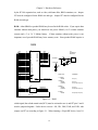
How to Connect It All
There are two different setups. The first is if you are using one of the two serial ports on the
Chickadee as the debugger port. The second is if you are using a third serial port on a PC/104
expansion board as the debugger port.
Debugger port on Chickadee:
1) Place the Chickadee on the table. Verify that the debugger kernel ROM is installed in U4
and the SRAM is installed in U6. Verify that standoffs are installed on the bottom side of
the Chickadee to prevent direct contact of the circuit board with the table surface.
2) Connect a red wire to JP12 pin 1. This is the positive (+) power supply feed.
3) Connect a black wire to JP12 pin 2. This is the negative (-) power supply feed, also called
“ground”. Note: instead of the connections to JP12 pin 1 and JP12 pin 2, you may connect
+5V to JP6 pin 4 and ground to JP6 pin 2, respectively.
5
Chapter 2: Setup
4) Connect the other end of the red (+) wire to the positive (+) terminal of your power
source. If the voltage regulator option is installed, the power source may be in the range of
7 to 26 VDC. If the voltage regulator option is not installed, the power source must be 5
+/- 0.2 VDC. Any voltage beyond these ranges may result in damage or improper
operation of the Chickadee.
5) Connect the other end of the black (-) wire to the negative (-) terminal of your power
source.
6) Turn the power source on. The red LED “RESET IND” should illuminate for a fraction of
a second, then extinguish. If it glows steadily or flickers, the voltage may be too low.
7) Turn the power source off.
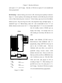
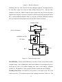
8) Connect the DB9F to DB9F null-modem serial adapter (crossover cable) to the DB9M on
your PC. See Fig. 2-1. If your PC’s serial port does not use a DB9M AT-style serial
connector, you will need an adapter.
9) Connect the JP11 or JP15 cable into whichever Chickadee serial port (JP11 or JP15) you
will be using for the debugger. Note that using JP15 for the debugger requires the second
RS-232 serial port option.
10) Connect the other end of the JP11 or JP15 cable to the free end of the DB9F to DB9F nullmodem serial adapter. Go to the section “Checking it Out”.
Fig. 2-1: Chickadee Development Setup
Debugger port on PC/104 expansion board:
1) Follow steps 1 - 9 of the “Debugger port on Chickadee” procedure.
6
Chapter 2: Setup
2) Attach the PC/104 expansion board to the Chickadee with standoffs. Be sure to engage all
PC/104 connector pins.
3) Verify that the interrupt jumpers and I/O address dipswitches on the PC/104 expansion
board are correct for the debugger configuration you will be using. Check the debugger
kernel ROM label for details.
4) Turn the power source on. The red LED “RESET IND” should illuminate for a fraction of
a second, then extinguish. If it glows steadily or flickers, the voltage may be too low.
5) Turn the power source off.
6) Attach the PC/104 expansion board serial cable to the PC/104 expansion board in the
manner prescribed by its user manual.
7) Attach the other end of the PC/104 expansion board serial cable to the free end of the
DB9F to DB9F null-modem serial adapter.
Checking it Out
It is assumed that the compiler you will use for software development is already installed on
your PC. If this is not so, install it now.
1) Install the Paradigm DEBUG/RT and LOCATE development software on your PC.
2) To check the serial link between your PC and the Chickadee, change to
C:\PDREM\UTILS (assuming drive C:) and type “RTTEST”.
This will invoke the
Paradigm PDREMOTE Test Aid. Set the baud rate to 115,200 (F5) and select the proper
port (F4). Press F2 several times to send nulls to the Chickadee and observe the responses
in the window. Exit (F9) the program. If this does not work, recheck your power and
serial cable connections, and PC/104 expansion board jumpers and dipswitches (if
applicable), and try again. If this still does not work, call Bagotronix technical support.
3) Insert the Sunflower C library floppy disk in your PC, create a directory
\CHICKADE\CSFC on your PC’s hard disk and copy the Sunflower C source files into
them.
4) Change to the \CHICKADE\CSFC directory. After reading the README.TXT file, run
your compiler and the Paradigm tools using the makefile to build the Sunflower C library
examples.
7
Chapter 2: Setup
5) Load some of the example programs. Try stepping through the code one line at a time.
You can even trace into Sunflower C library functions, since they still have debugging
information.
If your attempt to get started was unsuccessful, go back and examine each step to see if it was
done correctly. It is important to get this test working, since you will not be able to develop
your application software unless the Chickadee and your PC cooperate. Serial ports are
frequently troublesome. If your PC has a non-standard serial port, you are in for some
detective work.
8
Chapter 3: Hardware Reference
9
10
Chapter 3: Hardware Reference
Overview
This chapter contains information on how to use the Chickadee peripherals. It is assumed that
you are familiar with C and 8086 assembly language, possess a working knowledge of
electronics, and have access to data sheets of every key integrated circuit used in the Chickadee
design.
CPU
The Chickadee uses the 80C188 CPU, which comes in several variations.
Subject to
availability, compatible variants of the 80C188 may be substituted. Originally designed by
Intel, the 80C188 provides object code compatibility with the 8086.1 The 80C188 also has
several enhancements to the 8086 instruction set.2
The 80C188 has a memory address range of 1 MB. The I/O address range is 64 KB. The onchip peripherals include a power-save unit, interrupt control unit, timer/counter unit, chip select
unit, DMA unit, and refresh control unit. The CPU clock rate can range from 8 to 25 MHZ
depending on the grade of CPU and crystal installed.
Memory
Chickadee memory map:
00000h - 7FFFFh
RAM (1 chip)
80000h - (x-1)h
PC/104 expansion bus (if applicable)
(x)h - FFFFFh ROM (1 chip)
where x is the starting address for the Upper Chip Select (UCS) pin of the 80C188. The UCS
may be configured for any convenient size up to 256K inclusive.3 If it is desired to use a 512K
ROM, U5 must be factory configured to direct all memory accesses from 80000h to FFFFFh
to the ROM. Note that this configuration would preclude any use of these memory addresses
1
80C186EA/80C188EA User's Manual, (Intel Corporation, 1991), Chapter 2, p. 14.
2
Ibid., Appendix A, pp. 1-9.
3
Ibid., Chapter 6, p. 6.
11
Chapter 3: Hardware Reference
by the PC/104 expansion bus, such as video, solid state disks, BIOS extensions, etc. Jumper
JP3 must be configured for the ROM size and type. Jumper JP7 must be configured for the
RAM size and type.
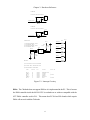
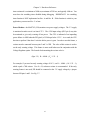
RAM: either SRAM or pseudo-SRAM may be used in the RAM socket. If you require data
retention without main power, you should use low power SRAM (1 to 2 uA data retention
current) and a 3 to 3.6 V lithium battery. If data retention without main power is not
important, use of pseudo-SRAM may lower memory costs. Since pseudo-SRAM requires a
RAM
U6
SA0
SA1
SA2
SA3
SA4
SA5
SA6
SA7
SA8
SA9
SA10
SA11
SA12
SA13
SA14
SA15
SA16
12
11
10
9
8
7
6
5
27
26
23
25
4
28
3
31
2
-CSRAM
-RD
-WR
CE2/SA17
22
24
29
30
A0
A1
A2
A3
A4
A5
A6
A7
A8
A9
A10
A11
A12
A13
A14
A15
A16
O0
O1
O2
O3
O4
O5
O6
O7
13
14
15
17
18
19
20
21
TO
EXTERNAL
BATTERY
SD0
SD1
SD2
SD3
SD4
SD5
SD6
SD7
D3
1
2
+
-
SIP\2P
VCC
SD[0..7]
C8
0.01
CE1
OE
WE
CE2
1
3
5
JP1
1
D4
VCCRAM
RFSH
1
-RFSH/SA18
JP7
VCC
CE2/SA17
SA17
2
VCCRAM
2
4
6
-REFRESH
-RFSH/SA18
SA18
HEADER3X2
RAM TYPE:
JUMPERS:
<= 32KX8
SRAM
JP7(1-3)
128KX8
SRAM
PSRAM
JP7(1-3)
JP7(1-3) & JP7(2-4)
256KX8
SRAM
PSRAM
JP7(3-5)
JP7(3-5) & JP7(2-4)
512KX8
SRAM
JP7(3-5) & JP7(4-6)
SA[0..19]
Figure 3-1: RAM
refresh signal, the refresh control unit (RCU) must be activated to use it, and JP7 pins 2 and 4
must be jumpered together. Useful device sizes are: 8K, 32K, 128K, 256K, and 512K, with
jumpers on JP7 set according to Figure 3-1. When inserting a 28-pin DIP device, leave U6
12
Chapter 3: Hardware Reference
socket pins 1,2, 31, and 32 empty. Note that a 512K device requires U5 to be installed and
factory programmed.
RAM Backup: connect a battery power source to JP1, observing correct polarity as shown in
Figure 3-1. Incorrect polarity will not damage the Chickadee or the RAM chip, but will result
in loss of data when main power is removed. Various battery types may be used, but lithium
batteries are best. They have long service life, wide temperature range, and high capacity. A
standard PC-type 3.6 V lithium battery works well. Also recommended are two 1.5 V AA
alkaline batteries wired in series for 3 V. Voltages higher than 3.6 V are not recommended
since the standby current of SRAM goes up
sharply with voltage. For example, three AA
ROM
cells actually give less battery life than two AA
U4
SA0
SA1
SA2
SA3
SA4
SA5
SA6
SA7
SA8
SA9
SA10
SA11
SA12
SA13
SA14
SA15
SA16
VCC/SA17
-CSROM
-RD
VCC
-WR/SA18
12
11
10
9
8
7
6
5
27
26
23
25
4
28
29
3
2
30
22
24
1
31
A0
A1
A2
A3
A4
A5
A6
A7
A8
A9
A10
A11
A12
A13
A14
A15
A16
A17
CE
OE
VPP
A18
O0
O1
O2
O3
O4
O5
O6
O7
13
14
15
17
18
19
20
21
SD0
SD1
SD2
SD3
SD4
SD5
SD6
SD7
SD[0..7]
USE 5V
FLASH
ONLY
VCC/SA17
SA17
either EPROM (27CXXX series) or
blocked/sectored flash EEPROM with 5 V
programming voltage (29FXXX series) may be
used in the U4 ROM socket.
With the
updateable storage, because erasure would
obliterate the boot code. However, bulk erase
JP3
1
3
5
ROM:
Chickadee, bulk erase flash is not useful for
27040
VCC
cells!
2
4
6
-WR
-WR/SA18
SA18
HEADER3X2
SA[0..19]
ROM TYPE:
JUMPERS:
<=128KX8
ROM
FLASH
JP3(1-3)
JP3(1-3) & JP3(2-4)
256KX8
ROM
FLASH
JP3(3-5)
JP3(3-5) & JP3(2-4)
512KX8
ROM
JP3(3-5) & JP3(4-6)
flash may still be used like an EPROM for boot
code. Useful device sizes are: 32K, 64K, 128K,
256K, and 512K, with jumpers on JP3 set
according to Figure 3-2. When inserting a 28pin DIP device, leave U4 socket pins 1,2, 31,
and 32 empty. Note that a 512K device requires
U5 to be installed and factory programmed.
Figure 3-2: ROM
13
Chapter 3: Hardware Reference
PC/104 Expansion Bus:
If your application needs only the built-in I/O on the Chickadee, there is no need to use the
PC/104 expansion bus. Otherwise, use of the PC/104 bus is necessary. The PC/104 bus
signals are listed in Table 3-1. Active low signals are designated by an asterisk (*).
Pin Number J1/P1 Row A Description
1
2
3
4
5
6
7
8
9
10
IOCHCHK*
SD7
SD6
SD5
SD4
SD3
SD2
SD1
SD0
IOCHRDY
11
12
13
14
15
16
17
18
19
20
21
22
23
24
25
26
27
28
29
30
31
32
AEN
SA19
SA18
SA17
SA16
SA15
SA14
SA13
SA12
SA11
SA10
SA9
SA8
SA7
SA6
SA5
SA4
SA3
SA2
SA1
SA0
GND
I/O Channel Check - input; not implemented, NC
System Data bit 7 - bidirectional 3-state with 10K pull-up resistor
System Data bit 6 - bidirectional 3-state with 10K pull-up resistor
System Data bit 5 - bidirectional 3-state with 10K pull-up resistor
System Data bit 4 - bidirectional 3-state with 10K pull-up resistor
System Data bit 3 - bidirectional 3-state with 10K pull-up resistor
System Data bit 2 - bidirectional 3-state with 10K pull-up resistor
System Data bit 1 - bidirectional 3-state with 10K pull-up resistor
System Data bit 0 - bidirectional 3-state with 10K pull-up resistor
I/O Channel Ready - input with 1K pull-up resistor; pull low to insert
wait states
Address Enable - output; not implemented, tied to GND
System Address bit 19 - output
System Address bit 18 - output
System Address bit 17 - output
System Address bit 16 - output
System Address bit 15 - output
System Address bit 14 - output
System Address bit 13 - output
System Address bit 12 - output
System Address bit 11 - output
System Address bit 10 - output
System Address bit 9 - output
System Address bit 8 - output
System Address bit 7 - output
System Address bit 6 - output
System Address bit 5 - output
System Address bit 4 - output
System Address bit 3 - output
System Address bit 2 - output
System Address bit 1 - output
System Address bit 0 - output
Ground
Table 3-1: PC/104 Expansion Bus Signals
14
Chapter 3: Hardware Reference
Pin Number J1/P1 Row B Description
1
2
3
4
5
GND
RESETDRV
+5V
IRQ2
-5V
6
7
DRQ2
-12V
8
9
ENDXFR*
+12V
10
11
12
13
14
15
16
17
18
19
20
21
(KEY)
SMEMW*
SMEMR*
IOW*
IOR*
DACK3*
DRQ3
DACK1*
DRQ1
REFRESH*
SYSCLK
IRQ7
22
23
24
IRQ6
IRQ5
IRQ4
25
26
27
28
IRQ3
DACK2*
TC
BALE
29
30
31
32
+5V
OSC
GND
GND
Ground
Reset Driver - output; active high when CPU is in reset
+5V power supply voltage
Interrupt Request 2 - input with 10K pull-up resistor
-5V power supply voltage - not required or generated by
Chickadee
DMA Request 2 - input; not implemented; NC
-12V power supply voltage - not required or generated by
Chickadee
End Transfer - input; not implemented; NC
+12V power supply voltage - not required or generated by
Chickadee
Ground - used for connector keying on some PC/104 systems
System Memory Write - output; active low
System Memory Read - output; active low
I/O Write - output; active low
I/O Read - output; active low
DMA Acknowledge 3 - output; not implemented; tied to +5V
DMA Request 3 - input; not implemented; NC
DMA Acknowledge 1 - output; not implemented; tied to +5V
DMA Request 1 - input; not implemented; NC
DRAM Refresh - output; connected to Refresh Control Unit
System Clock - frequency related to CPU clock
Interrupt Request 7 - input with 10K pull-up or 1K pull-down
resistor
Interrupt Request 6 - input with 10K pull-up resistor
Interrupt Request 5 - input with 10K pull-up resistor
Interrupt Request 4 - input with 10K pull-up or 1K pull-down
resistor
Interrupt Request 3 - input with 10K pull-up resistor
DMA Acknowledge 2 - output; not implemented; tied to +5V
Terminal Count - output; not implemented; tied to Ground
Bus Address Latch Enable - output; indicates valid address
when low
+5V power supply voltage
14.31818 MHz Oscillator - output; not implemented; NC
Ground
Ground
Table 3-1 (continued): PC/104 Expansion Bus Signals
As a minimum, interfacing to the PC/104 expansion bus requires I/O address decoding and
bidirectional transfer of data. Your application I/O hardware may also require memory address
decoding, interrupt requests, and wait states. Since most I/O hardware uses a small number of
consecutive byte addresses, it should be mapped into I/O space, not memory space. Memory
15
Chapter 3: Hardware Reference
space should only be used for RAM, ROM, EEPROM, video hardware, or highly specialized
I/O.
PC/104 Expansion Bus Timing: Proper synchronization with the PC/104 expansion bus is
essential for your I/O circuitry to function. If your I/O circuitry cannot keep up with the
Chickadee CPU, it must generate wait states. Wait states inform the CPU that the bus
operation currently in progress will take longer than usual. If the Chickadee CPU is clocked at
8 MHz or less and your I/O circuit uses LSTTL/HCMOS logic, you probably do not need to
use wait states. If the Chickadee CPU is clocked at 16MHz, you probably need to use at least
one wait state, or FAST/FACT logic. The speed limiting factors are usually the I/O devices,
such as peripheral interfaces, counters, A/D converters, UARTs, etc. These are usually much
slower than logic devices. For PC/104 expansion bus timings, refer to an ISA bus technical
reference4.
Interrupts: Interrupts can operate in two different modes: edge-sensitive and level-sensitive.
The PC/104 expansion bus mainly uses edge-sensitive interrupts, but either mode may be used.
In edge-sensitive mode, interrupt requests are made on the rising edge (low-to-high transition)
of the request pulse. In the level-sensitive mode, interrupt requests may occur as long as the
interrupt request line remains high.5 Two or more devices may share the same interrupt in
level-sensitive mode. The PC/104 expansion bus interrupt request lines are held high (or low)
by pull-up (or pull-down) resistors on the Chickadee. Do not use a push-pull (totem-pole) type
driver if you intend for two or more devices to share an interrupt. If an IRQn line is operated
in level-sensitive mode, your I/O circuitry must allow the IRQn line to be pulled low by a
resistor under normal conditions, and drive it high only during the interrupting condition. The
Chickadee interrupt circuitry is shown in Figure 3-3. Note that IRQ4 and IRQ7 can be jumper
configured for 1K pull-down or 10K pull-up resistors. IRQ2, IRQ3, IRQ5, and IRQ6 have
only 10K pull-up resistors on-board, but can use 1K pull-down resistors located on a PC/104
expansion board.
4
Several good technical references exist, such as Interfacing to the IBM Personal Computer, Second
Edition, Lewis C. Eggebrecht, (Howard W. Sams and Company), and IEEE-P996.
5
80C186EA/80C188EA User's Manual, Chapter 8, pp. 9-10.
16
Chapter 3: Hardware Reference
JUMPER:
1 - 2 N O N - S H A R E D IR Q 4
JP4
1
2
D 1
1
C O M 1 IR Q
2
IR Q 4
1N4148
JUMPER:
1 - 2 N O N - S H A R E D IR Q 7
JP5
1
2
D 2
1
C O M 2 IR Q
2
IR Q 7
1N4148
V C C
R 6
J U M P E R S :
V C C
1
1
6
6
-2
-3
-5
-4
NO
SH
NO
SH
N
A
N
A
-S H A R
R E D IR
-S H A R
R E D IR
E D IR Q 4
Q 4
E D IR Q 7
Q 7
IO R D Y
1K
R 9
10K
R 2
R 10
1K
IR Q 2
JP2
IR Q 4
1
3
5
10K
2
4
6
R 3
IR Q 3
IR Q 7
10K
HEADER3X2
R 7
1K
R 4
R 8
10K
IR Q 5
10K
V C C
R 5
IR Q 6
N O T E S :
10K
1) PC D M A N O T S U P P O R T E D
2) PC N M I N O T S U P P O R T E D
3 ) IN T E R R U P T M A P P IN G :
C P U
IN T 2
DMA1
IN T 0
IN T 1
DMA0
IN T 3
VEC#
E
B
C
D
A
F
P C
IR
IR
IR
IR
IR
IR
Q
Q
Q
Q
Q
Q
2
3
4
5
6
7
P C I/O
C P U I/O
R E S E R V E D
C O M 2
C O M 1
H A R D
FLO P P Y
LPT1
C O M 1
C O M 2
Figure 3-3: Interrupt Circuitry
DMA: The Chickadee does not support DMA as it is implemented in the PC. This is because
the DMA controller inside the 80C188 CPU is not hardware or software compatible with the
8237 DMA controller used in PCs. This means that PC/104 and ISA boards which require
DMA will not work with the Chickadee.
17
Chapter 3: Hardware Reference
In describing DMA use, a DMA operation refers to one or more read/write cycles of the DMA
unit, and a DMA transfer refers to a single read/write cycle. Thus, an operation is made up of
one or more transfers. DMA transfer timings are the same as read and write timings, except
for destination synchronized transfers, where two idle states are inserted at the end of the
deposit (write) cycle.6 Two consecutive bus cycles are required for a DMA transfer: one to
read the data from the source, and one to write the data to the destination. The DMA request
timing is as follows: to initiate the DMA operation, DRQn must be driven high for at least one
SYSCLK clock, and remain high for the duration of the DMA operation. DRQn must be
deasserted at least four clocks before the end of the DMA operation, or another DMA transfer
will begin, unless the TC (Terminal Count register) is programmed to limit the number of
DMA transfers. In the Chickadee, the DMA request inputs to the 80C188 are connected to
IRQ3 and IRQ6. Since the 80C188 does not support PC-style DMA, it makes sense to use the
DMA channels as interrupt request inputs. This is made to work by software which programs
the DMA channel to perform a dummy transfer and interrupt upon terminal count. In the
interrupt service routine, the DMA channel is rearmed and the interrupt request is
acknowledged.
See the Sunflower C library for precoded interrupt service routines to
implement this technique.
I/O Mapped Peripherals: The purpose of I/O address decoding is to generate chip select
signals for the peripheral chips on your PC/104 expansion board. The allowable range of I/O
addresses is 000h to 3FFh.
On-Board Peripherals:
A summary of the Chickadee on-board peripherals follows.
For connector pinouts see
Appendix A.
RS-232 Port:
the UART is 8250-compatible7 (16550 type optional), with RS-232
transceivers8 (MAX232) for transmit data (TX), receive data (RX), request to send (RTS), and
6
80C186EA/80C188EA User's Manual, Chapter 10, pp. 4-5.
7
Computer Products Data Manual, (VLSI Technology, Inc., 1990), Chapter 6, pp. 51-74.
18
Chapter 3: Hardware Reference
clear to send (CTS). An IDC connector and ribbon cable with DB9M plug form an AT-like
DTE device. Baud rates to 115.2K, with full or half duplex operation. RS-232 voltages are
generated on-board. COM1 is at I/O address 400h-407h (PC is 3F8h-3FFh) and uses IRQ4.
RS-232/485 Port: may be configured for either RS-232 or RS-485. The UART is 8250compatible (16550 type optional), with RS-232 transceivers for TX, RX, RTS, and CTS. An
IDC connector and ribbon cable with DB9M plug form an AT-like DTE device. Baud rates to
115.2K, with full or half duplex operation.
RS-232 voltages are generated on-board.
Alternatively, an RS-485 transceiver9 (75176 type) may be used, with half duplex operation to
115.2K baud. Surge protection and jumper selectable 100 ohm AC termination are provided
for RS-485 network connection. Optional galvanic isolation may be added by installing T1,
U24, and U26. COM2 is at I/O address 480h-487h (PC is 2F8h-2FFh) and uses IRQ7 (PC
uses IRQ3).
Peripheral Interface Adapter (PIA): the 7 relay driver outputs and the 16 TTL I/O are
controlled by a 82C55A PIA chip. Each PIA port pin is configured as an input upon power-up
or reset. Software must program each PIA port as either an input or an output.10 The
Sunflower C software library includes functions to program the PIA. The PIA is at I/O address
580h-583h. To use the 7 relay driver outputs, Port B must be configured for output. Any pin
configured as an output on Port A or C can sink 2.5 mA at 0.4 V or source 2.5 mA at 1.7 V,
thereby directly driving optoelectronic I/O modules. There is no need to connect pull-up
resistors to unused pins of the PIA, since each pin has an internal hold device to maintain a
stable state. However, it is mandatory to connect pull-up or pull-down resistors to inputs that
are connected to devices such as switches and open-collector drivers.
Relay Driver Outputs: for operating relays and solenoids up to 500 mA per output and 24V
(up to 50 V by special request - contact Bagotronix tech support). The current rating of each
8
1992 New Releases Data Book, (Maxim Integrated Products, 1991), Chapter 2, pp. 13-40.
9
Interface Circuits, (Texas Instruments, 1991), Chapter 5, pp. 577-586.
10
Peripherals, (Intel Corporation, 1990), Chapter 3, pp. 124-146.
19
Chapter 3: Hardware Reference
output depends on how many outputs are on at the same time, what currents are being driven,
and the ambient temperature. Use the following formulas to determine the limits for your
application:
(Eqn. 3-1) Allowable total power dissipation at a given ambient temperature:
PD = 0.95 - 0.0076 · (T - 25)
where T is in Celsius and PD is in watts
(Eqn. 3-2) Power dissipation of one output driver at a given load current:
PD = 0.75 IC + 2 IC2
where IC is in amperes and PD is in watts
(Eqn. 3-3) Allowable load current at a given power dissipation:
IC = [ - 0.75 + (0.5625 + 8 · PD)1/2 ] / 4
where IC is in amperes and PD is in watts
For example, an ambient temperature of 70 °C results in an allowable total power dissipation of
0.95 - 0.0076 · (70 - 25) = 0.608 W (Eqn. 3-1). If an output driver is driving a relay coil that is
rated at 110 mA, the power dissipation of that output driver is 0.75 · 0.110 + 2 · (0.110)2 =
0.107 W (Eqn. 3-2). From this example, it is shown that at most, five output drivers (0.608 W
/ 0.107 W) may simultaneously operate, each with a 110 mA load. Each output driver
contributes 0.107 W to the total power dissipation. It is possible to operate each output driver
with different loads. For example, at 70 °C one output may drive a solenoid at 300 mA (0.405
W), with four outputs driving 50 mA relay coils (0.043 W each).
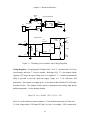
Each output is a NPN Darlington with a flyback diode to protect the output from damage due
to back-EMF when coils are de-energized. The relay driver output equivalent circuit is shown
in Fig 3-4. To turn on an output, write a 1 to its Port B bit. This will turn the transistor on,
sinking the load current.
20
Chapter 3: Hardware Reference
TO JP12
OCn
1
2
2
D18
PORT Bn
1
n = 0..6
Figure 3-4: Relay Driver Output Equivalent Circuit
Note:
even though the relay driver outputs are protected from back-EMF, it is still
recommended that each coil have its own flyback diode mounted as close to the coil terminals
as possible. This will reduce the amount of switching noise coupled into sensitive areas of your
system.
Optically Isolated AC/DC Inputs: for interfacing with equipment operating on different
voltages. AC and DC voltages from 3 to 48 V can be accommodated. The eight inputs are
split into two groups of four inputs, each group with its own common terminal. This allows
monitoring of two systems which are isolated from the Chickadee and each other. Polarity is
unimportant, since each optocoupler circuit has anti-parallel LEDs. The equivalent circuit is
shown in Fig 3-5.
21
Chapter 3: Hardware Reference
n = 0..7
p = 0 for n = 0..3
p = 1 for n = 4..7
VCC
R
In
1
4
ICOMp
2
3
BITn
Figure 3-5: Optically Isolated AC/DC Input
The bit polarity of the AC/DC inputs is inverted. A voltage present on an input will result in a
‘0’ being read from the status register. No voltage present will result in a ‘1’.
When monitoring AC signals, it is necessary to read the AC/DC inputs several times over an
interval related to the AC frequency. This is because the optocouplers will be extinguished
during AC zero crossing. For example, take the first reading. After 1/6 AC cycle (2.78 ms),
take the second reading. After another 1/6 AC cycle (2.78 ms), take the third reading. Then
take the best two of three to determine the input state: if there were two or more 0’s, then the
AC input is on; if there were two or more 1’s, then the AC input is off.
The Sunflower C library includes functions to operate the AC/DC inputs. IMPORTANT: the
optically isolated AC/DC inputs are NOT intended to isolate large potential differences, such as
AC power mains. The creep distance and pin spacing of the optocoupler circuitry are NOT
sufficient for 110 V and higher circuitry. This feature is mainly intended for isolating ground
paths where potential differences are never more than a few volts.
ADC: for interfacing up to eight channels of analog circuitry, sensors, measuring devices, etc.
with 12-bit resolution. The ADC (U9) is connected to the CPU by a serial “bit-bang” interface,
22
Chapter 3: Hardware Reference
therefore the ADC sample rate is limited by the CPU speed. An 8 MHz CPU is capable of
about 2K samples per second. A 25 MHz CPU is capable of about 6K samples per second.
Accurate A/D conversion requires a sample frequency at least twice the highest frequency in
the signal being measured. Due to sampling rate limitations of the Chickadee ADC, it is best
suited for DC and low frequency (less than 500 Hz) applications.
Depending on the desired mode of operation, one of three different ADCs may be installed in
U9 - a MAX186, MAX188, or LTC1296. The ADC reference can be either ratiometric
(MAX188 or LTC1296) or absolute (MAX186 only). With a ratiometric reference, the
Chickadee power supply voltage (5 V typical) is used as the ADC conversion reference, giving
a bit weight of 1.221 mV per LSB. Although the 5 V power to a system is rarely well
regulated, if transducers are capable of ratiometric output, then all errors due to reference
voltage drift and accuracy are eliminated. With an absolute reference, all conversions are made
to a 4.095 V reference voltage, giving a bit weight of 1 mV per LSB. The absolute reference
voltage (VREF) is available to your interface circuitry on JP10 pin 26. Do not load VREF by
more than 0.5 mA, or ADC accuracy may suffer. Also, do not change VREF loading during a
conversion. It is best to buffer VREF with an op-amp if you need the reference voltage for
your application circuitry. Unused ADC channels should be connected to ground. ADC input
voltages must not exceed the 5 V supply by more than 0.5 V, or damage may result.
ADC input voltages should not exceed the 5 V supply by more than 50 mV, or conversion
accuracy on other channels may be affected.
When an ADC conversion is initiated, the signal is first acquired by the ADC, then it is
converted.
High impedance sources may need extra time to charge the ADC internal
capacitance during acquisition. To calculate the acquisition time, use this formula:
(Eqn. 3-4) tAZ = 1.44 · 10-10 · (RS + 5000)
where tAZ is the time in seconds and RS is the internal resistance of the source
23
Chapter 3: Hardware Reference
For example, a sensor with an internal resistance of 100K needs 1.44 · 10-10 · (100000 + 5000)
= 0.000015 s or 15 us acquisition time. The Sunflower C library contains an ADC function
which allows you to specify the acquisition time in microseconds as an argument to the
function.
The ADC can be operated in either SE (single-ended) or DF (pseudo-differential) mode, or a
combination of both modes. In SE mode, the analog input voltage is referenced to ground. In
DF mode, two channels are paired, and the analog input voltage (+) is referenced to another
input voltage (-), not ground. DF mode has a restriction that the (-) input must be stable within
+/- 0.5 LSB with respect to ground during the conversion. This can be accomplished by
connecting a 0.1 uF capacitor between the (-) input and ground. Table 3-2 shows the possible
ADC channel combinations for DF mode.
Table 3-2: ADC DF Mode Channel Combinations
There are many hardware and software based techniques to eliminate noise in ADC
conversions. Hardware techniques include the use of shielded wire to carry signals, RC
filtering, active filtering, etc. Software based techniques include oversampling, averaging,
digital filtering, etc. One effective way to eliminate 60 Hz power line noise from ADC
conversions is to sample many times over a 60 Hz period (16.67 ms) and average all the
samples together. This has the effect of integrating the AC noise over the entire cycle to zero.
24
Chapter 3: Hardware Reference
Status Indicators: for indicating the current state of relay driver outputs, AC/DC inputs, and
serial ports. Each indicator when lit uses about 10 mA of current from the 5 V power supply,
so be sure to include them in your power budget. The serial port indicators are lit only when
the serial line is in the “0” state, therefore they flicker when data is being transferred.
LCD Port: for standard LCD modules to 4 lines by 40 characters per line which use the
Hitachi HD44780 or compatible display control LSI. Contrast voltage (+2/-5 V) is a function
of Timer 0 duty cycle, and may be adjusted by software. If Timer 0 is used for LCD contrast
adjustment, it is unavailable for other use. The Sunflower C library includes functions to
operate the LCD.
Keypad Port: for matrix keypads up to 4 columns by 4 rows. Storm series keypads or
compatibles may be used with no special wiring harness required. Individual switches may also
be used. The Sunflower C library includes functions to operate the keypad port.
Real Time Clock (RTC): a Dallas DS2404 (U13) combines a 32-bit real time counter with
512 bytes of non-volatile RAM. The Sunflower C library includes functions to operate the
RTC. The RTC output is capable of powering up the Chickadee and other equipment
connected to the -PWRUP pin (JP12 pin 3). This feature can be used to let the system turn
itself on at a previously programmed time and date, do some processing, set the time and date
for the next power up, and then turn itself off. No standby power is required. To use this
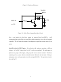
feature, a manual pushbutton, relay, and one of the Chickadee relay driver outputs is required.
Connect these items as shown in Fig. 3-6.
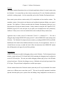
Theory of operation: at some time while the Chickadee is powered, the program sets the RTC
alarm registers to a value equal to the future time at which it should power up. Then the relay
driver output is turned off, resulting in breaking of the relay contacts and the disconnection of
power to the Chickadee. Time passes. When the RTC time registers match the alarm
registers, the -PWRUP output energizes the relay.
25
As the relay contacts engage, the
Chapter 3: Hardware Reference
Chickadee powers up. After reset, the CPU starts running the program. The program turns on
the relay driver output, then clears the alarm condition from the RTC. After the alarm
condition is cleared, the -PWRUP output no longer energizes the relay, but the relay driver
output keeps it energized. If powerup is required at a time not previously programmed into the
RTC, a manual pushbutton should be added. It is necessary to hold the pushbutton in until the
CPU gets to the place in the program where the relay driver output is turned on.
MANUAL START
RELAY
Vsupply
+VIN (To Chickadee)
Q3
POWERUP OUTPUT
RTC Alarm
<--PWRUP
3
2
1
<-OCn
1
2
2
D18
BITn
1
RELAY DRIVER OUTPUT
Figure 3-6: Timed Powerup Circuit
0.5K EEPROM: a 24C04 serial EEPROM (U8) provides 512 bytes of nonvolatile erasable,
rewritable storage. Since EEPROM has a finite write endurance of several thousand cycles, it
should only be used to store seldom changing data, such as serial numbers, calibration
constants, etc. The Sunflower C library includes functions to operate the serial EEPROM.
Watchdog Timer Reset: the MAX705 (U10) provides a reset signal to the CPU if the
software goes awry. Your software must reset the watchdog timer before it times out. The
26
Chapter 3: Hardware Reference
time-out interval is a minimum of 1000 ms, maximum of 2250 ms, and typically 1600 ms. You
must leave the watchdog timer disabled during debugging. IMPORTANT: the watchdog
timer function is NOT implemented on Rev. A and Rev. B. If this function is critical to your
application, you must use Rev. C or later.
Power Monitor: the MAX705 (U10) monitors two power supply voltages. The 5 V supply
is monitored to make sure it is at least 4.75 V. The +VIN input voltage (JP12 pin 1) may also
be monitored to give early warning of lost power. The CPU is informed of an impending
power failure via NMI when the PFI (pin 4) of U10 drops below 1.25 V. As a result, the CPU
has time to perform "shut down" activities before power is gone. In order to use this feature, a
resistor must be connected between pins 2 and 3 of JP8. The value of this resistor is used to
set the early warning voltage. This feature is most useful when used in conjunction with the
Voltage Regulator option. The formula for determining the resistor value is:
(Eqn. 3-5) R = 10000 · (Vin / 1.25 - 1)
For example, if you need an early warning voltage of 10 V, use R = 10000 · (10 / 1.25 - 1),
which equals a 70K resistor. Use of a 1% tolerance resistor is recommended. If the early
warning feature is not used, PFI should be connected to the 5 V supply voltage by a jumper
between JP8 pins 1 and 2. See Fig. 3-7.
27
Chapter 3: Hardware Reference
RESET
SW1
VOLTAGE MONITOR
1
4
2
3
U10
1
2
3
4
EVQ-PA
Vth ADJUST
VCC
JP8
1
2
3
VCC
MR
VCC
GND
PFI
R24
WDO
RESET
WDI
PFO
8
7
6
5
NC
-RESET
NC
-NMI
R23
100K
MAX705CSA
10.0K
1% MF
SIP\3P
POWER SUPPLY
VCC
R32
3.01K
1% MF
U15
LM2941T
D11
+VIN 1
4
2
VIN
HER103
2
GND
D17
C12
470
50V
C13
1
CER
50V
2
ON/OFF
1
5
V
O
U
T
G
N
D
C11
22
TANT
1
ADJ
R40
500
1 2
5V ADJ
3
3
R31
1.00K
1% MF
Figure 3-7: Watchdog, Power Monitor, and Voltage Regulator
Voltage Regulator: for operating the Chickadee from 7 to 26 V. Operation above 26 V may
cause damage, and below 7 V may be unstable. Referring to Fig. 3-7, a low-dropout voltage
regulator (U15) drops the input voltage down to a regulated 5 V. A trimmer potentiometer
(R40) is provided to precisely adjust the supply voltage to 5 V for ratiometric A/D
applications. The regulator can supply up to 1 A of current for the Chickadee, PC/104 boards,
and other circuitry. The regulator current capacity is dependent on the voltage input and the
ambient temperature. Use this derating formula:
(Eqn. 3-6) IMAX = 0.0385 · (150 - T) / (VIN - 5.6)
where IMAX is the maximum current in amperes, T is the ambient temperature in Celsius, and
VIN is the voltage on the +VIN input (JP12 pin 1) in volts. For example, +VIN is connected to
28
Chapter 3: Hardware Reference
15 V and the ambient temperature is 70 ºC. The maximum current the regulator can supply
under this condition is 0.0385 · (150 - 70) / (15 - 5.6) = 0.33 A.
It is possible to get more current capacity from the regulator if a bigger heat sink is used.
Contact Bagotronix tech support to discuss this before doing so.
Transient protection is provided when the Chickadee is equipped with the voltage regulator
option. Diode D17 is a transzorb which clamps at about 27 V. Capacitor C12 helps filter any
ripple which may be present. Diode D11 gives protection from reverse polarity.
Processor Failure Indicator: an LED (RESET IND) illuminates when the CPU is in reset.
Reset can be caused by actuation of the reset pushbutton, watchdog time-out (if enabled), or
supply voltage below the MAX705 (U10) power-on reset threshold. If RESET IND blinks, it
indicates that 1) the CPU is resetting but the code is bombing (if watchdog is enabled), 2) the
supply voltage is marginal, or 3) circuitry failure.
Reset Pushbutton:
with the normally open pushbutton switch SW1, the CPU can be
manually reset at any time. Use caution before using the reset switch in your control system.
See Fig. 3-7.
29
Chapter 3: Hardware Reference
30
Chapter 4: Software Development
31
32
Chapter 4: Software Development
Overview
This chapter contains information on how to develop the application software for control systems using
the Chickadee. It is assumed that you have already connected your PC to the Chickadee and that the
serial link is working properly. It is also assumed that you have the Chickadee Development System.
Most control system software consists mainly of I/O manipulation and user interface routines. The
remainder consists of data analysis and reduction and conditional statements defining your system’s
operation. The Sunflower C libraries provided with the Chickadee Development System give you a
head start on the I/O and user interface routines. Library routines for using the ADC, digital I/O, RTC,
EEPROM, keypad, LCD, and serial ports let you spend your development time more productively.
Sunflower C library source code is also included if the need to modify the library routines arises.
Application code is written on the PC in Microsoft C/Visual C++ or Borland C/C++. The code is
debugged using Paradigm DEBUG/RT running on the PC, and the DEBUG/RT kernel running on the
Chickadee. The Chickadee Development System contains a preconfigured DEBUG/RT kernel ROM.
Modification of the kernel in these ROMs should not be necessary for most applications. However, if
it should become necessary to modify the kernel, follow the instructions in the DEBUG/RT manual,
then call Bagotronix tech support if you still have problems.
Debugging Port
An RS-232 serial port is needed for debugging software on the Chickadee. The Development System
includes a single serial port PC/104 board and a ROM containing the debugging kernel configured to
use the PC/104 serial port. The extra port enables debugging without tying up any of the Chickadee
on-board serial ports. If desired, the debugger can use a Chickadee on-board serial port instead of the
PC/104 port. This special kernel configuration is available upon request.
Galvanic isolation between the Chickadee control system and your PC may be desirable if the control
system uses a different power source than your PC. This may be especially important for machines
operated from three phase power systems where the building wiring configuration is not known or is
33
Chapter 4: Software Development
known to be troublesome. In this case, the Chickadee RS-232/485 port may be equipped with the
galvanic isolation option and used as a debugger port.
C Startup Code
Every C program requires startup code. Startup code conditions the computer system to be able to run
the program that you have written. Even before the call to main(), some work must be done to set up
the stack, copy initialized variables from ROM to RAM, set aside the heap memory space, etc. In the
case of programs which run on the PC, this is taken care of for you by the Microsoft C/Visual C++ and
Borland C/C++ compilers. Each comes with its own startup code which is inserted during linking.
Since the Chickadee is an embedded computer system, it needs different startup code than that which
comes with the C compilers. The Chickadee does not have the same hardware and operating system
resources that a PC does, so its startup code must be different. Fortunately, LOCATE comes with
startup code that is suitable for embedded computer systems. When you are debugging during the
software development stage, the LOCATE configuration file should be edited so that processor
initialization directives are not included in the startup code for your application. When you are
satisfied with your application software and ready to burn it into an EPROM, the LOCATE
configuration file should be edited so that processor initialization directives are included in the startup
code. The procedures are different because the processor initialization is done by the kernel when it
starts up. At the end of application software development, the kernel is no longer needed, so the
processor initialization must be done by the same startup code that goes with the application program.
Processor initialization directives should not need to be changed for your application unless you intend
to use hardware other than that shipped with the Development System. Refer to the 80C188 data
sheet for details on the programmable chip selects and refresh control unit.
34
Chapter 4: Software Development
Your Application Software
Before you begin coding your application, take the time to print out or browse the Sunflower C
Library source files. You will find that most, if not all, of the routines needed to operate I/O are
already done for you.
Use your imagination to think of ways to use the Chickadee's features in your product. For example, a
menu system using several redefinable keys on a keypad located just under the bottom line in a multiline LCD. The text on the bottom line of the LCD could change to indicate context-sensitive functions
of the keys.
The RS-232 port could be connected to a modem for teleservicing and remote
monitoring. If flash memory is also used, software updates and bug fixes could be uploaded via
modem. There are many possibilities.
If it is not possible to connect your I/O hardware to the actual machine (or is dangerous to do so), you
should consider building a simulation apparatus for software testing. This could be as simple as
potentiometers used to simulate transducer inputs and toggle switches for digital inputs, or as elaborate
as rack mounted test equipment under control of a computerized stimulus generation program. For
most situations, a pot-and-switch rig is sufficient.
Once the Chickadee is connected to the PC and power supply and the debugger kernel works, you are
ready to begin software development. Link the startup code, compiler libraries, Sunflower C libraries,
and your compiled program together. Make sure the memory model is the same for all program
modules and libraries. Don't forget to tell the compiler to include symbolic debugging information in
the EXE. When linking is finished, use LOCATE to produce an absolute (AXE) file, then send the
AXE to the Chickadee via DEBUG/RT. Then debug your program.
Things to Watch Out For
Unless you have a ROMable DOS and BIOS installed, do not use DOS or BIOS function calls. Since
there is no DOS or BIOS, your program will bomb if you do so. Be careful of the Microsoft C/Visual
C++ and Borland C/C++ libraries. Many of the functions in these libraries use DOS or BIOS calls but
do not document this crucial fact. If a particular library function is suspect, instruct the compiler to
35
Chapter 4: Software Development
compile to assembly, then manually check the resulting ASM file. If it contains any INT 21h (DOS) or
INT 10h-1Fh (BIOS) calls, you cannot use that library function in your application. For malloc( ) and
other essentials, LOCATE provides an alternate library that does not use DOS or BIOS calls. If you
desire a ROMable DOS, call Bagotronix for details.
Unless you really need floating point in your application, try to do without it. The C floating point
emulation libraries are not reentrant, so they are of limited use for multitasking control programs
(special reentrant libraries do exist). Many computations can be performed with satisfactory precision
using integer arithmetic or lookup tables. Floating point will increase the size of your code and slow it
down when calculations are being performed. Integer (16-bit) and long integer (32-bit) calculations are
much faster. Fractional quantities can be expressed as integers if an artificial decimal point is inserted.
Example: if you are measuring fluid volume to the nearest hundredth liter, an unsigned integer variable
gives you a range of 0.00 to 655.35 liters with a resolution of 0.01 liters. On the other hand, if you
have the ROM space and the CPU time, do what you like.
Sunflower C Library
As you look through the source code of the library functions, you may notice there are conditional
compilation directives for the PC. These directives enable the library functions to be used on the PC as
well as the Chickadee. This might be useful if, for example, the Chickadee is part of a remote machine
monitoring system, and the PC is the data collector. By changing a #define and recompiling, you could
use the serial port functions both on the Chickadee and on the PC. Be sure to keep the Chickadee and
PC libraries in separate directories.
36
Chapter 5: Interrupts
37
38
Chapter 5: Interrupts
Overview
Interrupts are so fundamental to I/O and control applications, an entire chapter on this topic is
warranted. Since hardware and software interrupts occur due to different circumstances, only
hardware interrupts will be covered in this chapter. Getting interrupts to function correctly can
require a great deal of thought and patience. With the Sunflower C library, most the software
work has already been done for you. However, you do need to understand the underlying
principles to be assured that your software works the way you want it to.
In the discussions that follow, occasional references are made to PC interrupts. It is necessary
to understand PC interrupts only if you intend to use some of the Sunflower C functions on the
PC. This might be desirable, for example, if your application requires the Chickadee to
communicate with a PC via a serial port. Recompiling the Sunflower C COMM functions for
the PC would supply you with both sides of the communication software solution.
Brief Review: 80x86 Interrupts
The 80x86 family of microprocessors has a table of 256 interrupt vectors located in the first
1KB of address space (00000h - 003ffh). Each interrupt vector consists of a segment and
offset which correspond to the address of the interrupt service routine for that interrupt. When
a hardware or software interrupt occurs, the FLAGS are pushed onto the stack, followed by
the CS and IP registers. The CS and IP registers are then loaded with the address of the
interrupt service routine (ISR) that is associated with that vector. Execution of the ISR begins
and continues until the IRET instruction. The old IP, CS, and FLAGS are then popped off the
stack and program execution continues at the point where it was interrupted.11
The Interrupt Control Unit
On both the Chickadee and the PC, an Interrupt Control Unit (ICU) is responsible for handling
the interaction between requesting sources and the CPU. On the PC, the ICU is an 8259 or a
11
80C186EA/80C188EA User's Manual, (Intel Corporation, 1991), Chapter 2, pp. 34-36.
39
Chapter 5: Interrupts
compatible chip set. On the Chickadee, the ICU is inside the 80C188 itself. The Chickadee
and PC ICU's are not software compatible.
With the proper software, interrupts IRQ4 and IRQ7 may be shared. Interrupt service routines
(ISR) may either be chained or handled by a master ISR. Examples of each follow.
One interrupt source:
void interrupt isr (void) {
/* your interrupt handler */
/* some code */
}
.
.
disable( );
/* disable interrupts */
/* do not use compiler’s setvect-it has a DOS call */
setvect (IRQ4_VEC, isr);
/* LOCATE’s setvect ( ) */
enable( );
/* enable interrupts */
Two or more interrupt sources using chaining:
When chaining interrupts, a vector is initially set with the address of an ISR. Later, the same
vector is saved in a program variable, and then set with the address of another ISR. This new
ISR must contain a test to determine if its requesting source caused the interrupt. If not, the
old ISR is called.
void interrupt (*oldvect)( );
/* ptr to interrupt func */
void interrupt isr1 (void) {
/* some code */
}
void interrupt isr2 (void) {
if ( /* test condition goes here */ ) {
/* I did it. Handler code goes here. */
40
Chapter 5: Interrupts
}
else
/* Not me! Must have been the first ISR. */
oldvect( );
/* call first ISR */
}
.
.
disable();
/* disable interrupts */
/* setting vector to first isr; do not use compiler setvect-it has a DOS call */
setvect (IRQ4_VEC, isr1);
/* LOCATE’s setvect ( ) */
enable( );
/* enable interrupts */
.
.
/* storing vector to first isr; do not use compiler getvect - it has a DOS call */
oldvect = getvect (IRQ4_VEC);
/* LOCATE’s getvect ( ) */
disable( );
/* disable interrupts */
setvect (IRQ4_VEC, isr2); );
/* LOCATE’s setvect ( ) */
enable( );
/* enable interrupts */
Be sure to install the ISR which must be serviced with the least delay last, since it will be
processed first when the interrupt occurs.
Two or more interrupt sources using master ISR:
When using a master ISR, the interrupt functions must be rewritten as "pseudo-ISRs", that is,
normal C functions returning type int and taking no arguments. The returned value indicates
whether the called pseudo-ISR handled the request. If not, the next pseudo-ISRs are called in
sequence until one handles the request or all four have been called.
void interrupt MasterISR (void);
int isr1 (void) {
if ( /* test condition goes here */ ) {
/* I did it. Handler code goes here. */
41
Chapter 5: Interrupts
return 1;
/* return 1 indicating it was me */
}
else
/* Not me! Must have been some other ISR. */
return 0;
/* return 0 indicating it wasn't me */
}
int isr2 (void);
int isr3 (void);
/* similar to above */
.
.
disable( );
setvect (IRQ4_VEC, MasterISR);
IRQ4setvect (1, isr1);
/* put in master ISR slot 1 */
IRQ4setvect (2, isr1);
/* slot 2 */
IRQ4setvect (3, isr1);
/* slot 3 */
enable( );
There are special considerations with this approach. The function IRQ4setvect( ), which must
be written by you, fills an element of an array of function pointers with the function pointer
passed to it, in the element index passed to it. MasterISR( ), also written by you, is the actual
ISR processed when the interrupt occurs. MasterISR( ) calls each pseudo-ISR in sequence
until a value of 1 is returned. At this point, MasterISR( ) knows that the interrupt has been
serviced by the proper pseudo-ISR, and now may return from the interrupt.
If using a small program model (near code only), near pointers to the pseudo-ISRs are okay. If
using a large program model (far code), far pointers to the pseudo-ISRs are required. You
must also be careful not to call a null function pointer.
42
Chapter 5: Interrupts
End-of-interrupt (EOI)
An EOI is required to reset the ICU after servicing any hardware interrupt.12 Example:
void interrupt TypicalISR (void) {
/* some code */
.
.
NEOI( );
/* non-specific end-of-interrupt */
}
On the Chickadee, a non-specific EOI is issued with the following C code:
NEOI( );
/* see chickade.h header file for macro def */
When the interrupting ICU line is in level-triggered mode, do not issue EOI until the
interrupting condition has been reset and the ICU line has returned to a low logic level.
Otherwise, recursive interrupts will occur, resulting in stack overflow and a program crash.
Tips
1) When setting an interrupt vector, disable interrupts before and enable them afterwards.
This prevents the remote chance of a interrupt occurring halfway through the vector setting
process, which would cause a program crash.
2) If using DOS, do not call DOS functions from an interrupt handler. Doing so will cause a
program crash because DOS is not reentrant. Also, if you are using a multitasking executive,
you must restrict access to DOS to only one task at a time.
12
80C186EA/80C188EA User's Manual, (Intel Corporation, 1991), Chapter 8, p. 5.
43
Chapter 5: Interrupts
3) When using chained interrupts, install the interrupt needing the least latency last. This
makes it the first to execute when the interrupt occurs.
4) If insertion and removal of multiple ISR's is required, the master ISR technique must be
used. An ISR can be removed by setting a NULL vector. The calling order can be changed
also, allowing for latency adjustments if needed.
5) The master ISR technique is more efficient than chaining for more than two interrupt
sources.
6) When using C++ and multitasking, beware of the new( ) and delete( ) operators, since they
handle heap memory by calling malloc( ) and free( ). This process is not reentrant. A program
crash could occur if a task gets preempted during instantiation of an object, and the new task
instantiates another object. Since the previous hidden call to malloc( ) was not finished, the
heap could be corrupt. The solutions to this problem are 1) do not use C++ dynamic objects,
2) guard all C++ dynamic object instantiations with a semaphore, or 3) modify the malloc( )
function in the LOCATE library to guard itself with a built-in semaphore.
recommendations apply to free( ) and the destruction of C++ dynamic objects.
44
The same
Appendix A: I/O and Memory Address Map
45
46
Appendix A: I/O and Memory Address Map
I/O Address Map
The 80C188 Chip Select Unit must be programmed after reset to locate the on-board
peripherals in I/O space in accordance with this mapping. All I/O address are in hexadecimal.
* No hardware implementation
** Used for other purpose
000 - 3FF
Available to PC/104
80C188 -PCS0: 400 - 47F
400 - 407
COM1 16C450 or 16C550 UART:
400
RBR (Receive Buffer Register) (read only, DLAB = 0)
400
THR (Transmit Holding Register) (write only, DLAB = 0)
400
DLL (Divisor Latch LSB) (DLAB = 1)
401
DLM (Divisor Latch MSB) (DLAB = 1)
401
IER (Interrupt Enable Register) (DLAB = 0):
Bit 0
ERBFI (Enable Received Data Available Interrupt)
Bit 1
ETBEI (Enable Transmitter Holding Register Empty Interrupt)
Bit 2
ELSI (Enable Receiver Line Status Interrupt)
Bit 3
EDSSI (Enable Modem Status Interrupt)
Bit 4-7 Reserved (write as 0)
402
IIR (Interrupt Identification Register) (read only):
Bit 0
“0” If Interrupt Pending
Bit 1
Interrupt ID Bit 0
Bit 2
Interrupt ID Bit 1
Bit 3
Interrupt ID Bit 2 (16C550 only, 16C450 = 0)
Bit 4-5 Reserved
Bit 6-7 FIFOs Enabled
402
FCR (FIFO Control Register) (16C550 only, write only):
Bit 0
FIFO Enable
Bit 1
RCVR FIFO Reset
47
Appendix A: I/O and Memory Address Map
Bit 2
XMIT FIFO Reset
Bit 3
DMA Mode Select
Bit 4-5 Reserved (write as 0)
403
404
Bit 6
RCVR Trigger LSB
Bit 7
RCVR Trigger MSB
LCR (Line Control Register):
Bit 0
WLSB0 (Word Length Select Bit 0)
Bit 1
WLSB1 (Word Length Select Bit 1)
Bit 2
STB (Number of Stop Bits)
Bit 3
PEN (Parity Enable)
Bit 4
EPS (Even Parity Select)
Bit 5
Stick Parity
Bit 6
Set Break
Bit 7
DLAB (Divisor Latch Access Bit)
MCR (Modem Control Register):
Bit 0
DTR (Data Terminal Ready) *
Bit 1
RTS (Request To Send)
Bit 2
Out 1 *
Bit 3
INT (Interrupt Pin Enable)
Bit 4
Loop
Bit 5-7 Reserved (write as 0)
405
LSR (Line Status Register):
Bit 0
DR (Data Ready)
Bit 1
OE (Overrun Error)
Bit 2
PE (Parity Error)
Bit 3
FE (Framing Error)
Bit 4
BI (Break Interrupt)
Bit 5
THRE (Transmitter Holding Register Empty)
Bit 6
TEMT (Transmitter Empty)
Bit 7
Error in RCVR FIFO (16C550 only)
48
Appendix A: I/O and Memory Address Map
406
407
408 - 47F
MSR (Modem Status Register):
Bit 0
DCTS (Delta Clear To Send)
Bit 1
DDSR (Delta Data Set Ready) *
Bit 2
TERI (Trailing Edge Ring Indicator) *
Bit 3
DRSLD (Delta Receive Line Signal Detect) *
Bit 4
CTS (Clear To Send)
Bit 5
DSR (Data Set Ready) *
Bit 6
RI (Ring Indicator) *
Bit 7
DCD (Data Carrier Detect) *
SCR (Scratch Register)
Reserved
80C188 -PCS1: 480 - 4FF
480 - 487
COM2 16C450 or 16C550 UART:
480
RBR (Receive Buffer Register) (read only, DLAB = 0)
480
THR (Transmit Holding Register) (write only, DLAB = 0)
480
DLL (Divisor Latch LSB) (DLAB = 1)
481
DLM (Divisor Latch MSB) (DLAB = 1)
481
IER (Interrupt Enable Register) (DLAB = 0):
Bit 0
ERBFI (Enable Received Data Available Interrupt)
Bit 1
ETBEI (Enable Transmitter Holding Register Empty Interrupt)
Bit 2
ELSI (Enable Receiver Line Status Interrupt)
Bit 3
EDSSI (Enable Modem Status Interrupt)
Bit 4-7 Reserved (write as 0)
482
IIR (Interrupt Identification Register) (read only):
Bit 0
“0” If Interrupt Pending
Bit 1
Interrupt ID Bit 0
Bit 2
Interrupt ID Bit 1
Bit 3
Interrupt ID Bit 2 (16C550 only, 16C450 = 0)
Bit 4-5 Reserved
49
Appendix A: I/O and Memory Address Map
Bit 6-7 FIFOs Enabled
482
FCR (FIFO Control Register) (16C550 only, write only):
Bit 0
FIFO Enable
Bit 1
RCVR FIFO Reset
Bit 2
XMIT FIFO Reset
Bit 3
DMA Mode Select
Bit 4-5 Reserved (write as 0)
483
484
Bit 6
RCVR Trigger LSB
Bit 7
RCVR Trigger MSB
LCR (Line Control Register):
Bit 0
WLSB0 (Word Length Select Bit 0)
Bit 1
WLSB1 (Word Length Select Bit 1)
Bit 2
STB (Number of Stop Bits)
Bit 3
PEN (Parity Enable)
Bit 4
EPS (Even Parity Select)
Bit 5
Stick Parity
Bit 6
Set Break
Bit 7
DLAB (Divisor Latch Access Bit)
MCR (Modem Control Register):
Bit 0
DTR (Data Terminal Ready) *
Bit 1
RTS (Request To Send)
Bit 2
Out 1 *
Bit 3
INT (Interrupt Pin Enable)
Bit 4
Loop
Bit 5-7 Reserved (write as 0)
485
LSR (Line Status Register):
Bit 0
DR (Data Ready)
Bit 1
OE (Overrun Error)
Bit 2
PE (Parity Error)
Bit 3
FE (Framing Error)
50
Appendix A: I/O and Memory Address Map
486
487
488 - 4FF
Bit 4
BI (Break Interrupt)
Bit 5
THRE (Transmitter Holding Register Empty)
Bit 6
TEMT (Transmitter Empty)
Bit 7
Error in RCVR FIFO (16C550 only)
MSR (Modem Status Register):
Bit 0
DCTS (Delta Clear To Send)
Bit 1
DDSR (Delta Data Set Ready) *
Bit 2
TERI (Trailing Edge Ring Indicator) **
Bit 3
DRSLD (Delta Receive Line Signal Detect) **
Bit 4
CTS (Clear To Send)
Bit 5
DSR (Data Set Ready) *
Bit 6
RI (Ring Indicator, used by ADC SSTRB line) **
Bit 7
DCD (Data Carrier Detect, used by AC/DC Shift Register Output) **
SCR (Scratch Register)
Reserved
80C188 -PCS2: 500 - 57F
500 - 503
500
501
Bit-Bang Port (used for RTC, EEPROM, ADC, AC/DC inputs, LCD, keypad)
Data:
Bit 0
Not used
Bit 1
LCD Register Select
Bit 2
LCD Data Bit 4
Bit 3
LCD Data Bit 5
Bit 4
LCD Data Bit 6
Bit 5
LCD Data Bit 7, AC/DC Shift/Load
Bit 6
LCD Enable 1
Bit 7
LCD Enable 2
Status (read only):
Bit 0-2 Reserved
Bit 3
ERROR (Serial Data In)
51
Appendix A: I/O and Memory Address Map
502
Bit 4
SLCT (Keypad Row B)
Bit 5
PE (Keypad Row A)
Bit 6
ACK (Keypad Row D)
Bit 7
BUSY (Keypad Row C)
Control:
Bit 0
STROBE (Serial Clock)
Bit 1
AUTOFD (ADC Chip Select)
Bit 2
INIT (RTC Chip Select)
Bit 3
SLIN (Serial Data I/O)
Bit 4-7 Not used
503
504 - 57F
Not used
Reserved
80C188 -PCS3: 580 - 5FF
580 - 583
580
82C55 PIA
Port A:
Bit 0-7 TTL I/O on JP11
581
Port B:
Bit 0-6 Relay driver outputs on JP12 pins 4-10
Bit 7
582
Reserved (write as 0)
Port C:
Bit 0-7 TTL I/O on JP11
583
Control Word:
Bit 0
Port CL I/O
Bit 1
Port B I/O
Bit 2
Mode Selection Group B
Bit 3
Port CH I/O
Bit 4
Port A I/O
Bit 5-6 Mode Selection Group A
Bit 7
Mode Set Flag
52
Appendix A: I/O and Memory Address Map
584 - 5FF
Reserved
80C188 -PCS4: 600 - 67F
600 - 67F
Reserved
80C188 -PCS5: 680 - 6FF
680 - 6FF
Reserved
80C188 -PCS6: 700 - 77F
700
Watchdog
701 - 77F
Reserved
780 - FEFF
Reserved
80C188 PCB (Peripheral Control Block): FF00 - FFFF
Consult the Intel 80C188 User’s Manual or ApBUILDER for the following peripherals:
•
Peripheral Control Block
•
Chip Select Unit
•
Refresh Control Unit
•
Interrupt Controller Unit
•
Timer/Counter Unit
•
DMA Unit
•
Power Management Unit
53
Appendix A: I/O and Memory Address Map
Memory Address Map
The 80C188 Chip Select Unit must be programmed after reset to locate the on-board memory
in accordance with this mapping. All memory address are in hexadecimal.
RAM:
128K RAM (-LCS generated chip select):
00000 - 1FFFF
SRAM
20000 - 7FFFF
Available to PC/104
256K RAM (-LCS generated chip select):
00000 - 3FFFF
SRAM
40000 - 7FFFF
Available to PC/104
512K RAM (U5 generated chip select):
00000 - 7FFFF
SRAM
ROM:
64K ROM (-UCS generated chip select):
80000 - EFFFF
Available to PC/104
F0000 - FFFFF
ROM
128K ROM (-UCS generated chip select):
80000 - DFFFF
E0000 - FFFFF
Available to PC/104
ROM
256K ROM (-UCS generated chip select):
80000 - BFFFF
Available to PC/104
C0000 - FFFFF
ROM
54
Appendix A: I/O and Memory Address Map
512K ROM (U5 generated chip select):
80000 - FFFFF
ROM
In addition to the standard ROM sizes shown, odd ROM sizes can be accommodated using U5
to generate the ROM chip select.
For example, you may want a 192K ROM from
D0000 - FFFF and PC/104 from 80000 - CFFFF. In this case, a 256K ROM and special
programming of U5 would make 192K of the 256K ROM available for use, and the 64K
remainder available for PC/104. Contact Bagotronix tech support if you need a special
memory map.
55
Appendix A: I/O and Memory Address Map
56
Appendix B: Interrupt Map
57
58
Appendix B: Interrupt Map
Interrupt Map
Consult the Intel 80C188 User’s Manual or ApBUILDER regarding the use of any interrupts
not listed here. This listing is only for hardware interrupts used in the Chickadee.
Vector # (hex)
Vector Stored At (hex)
Description
2
00008
NMI (used by voltage monitor)
8
00020
Timer 0 (used by LCD contrast)
A
00028
DMA0 (used as IRQ6)
B
0002C
DMA1 (used as IRQ3)
C
00030
INT0 (used as IRQ4)
D
00034
INT1 (used as IRQ5)
E
00038
INT2 (used as IRQ2)
F
0003C
INT3 (used as IRQ7)
12
00048
Timer 1
13
0004C
Timer 2
Interrupt Assignments
IRQ2
PC/104
IRQ3
PC/104
IRQ4
On-board COM1 (can be shared with PC/104)
IRQ5
PC/104
IRQ6
PC/104
IRQ7
On-board COM2 (can be shared with PC/104)
59
Appendix B: Interrupt Map
60
Appendix C: Connections
61
62
Appendix C: Connections
The following header pin tables are referenced to the component side of the PCB. Except as
noted, pin 1 is a square pad. Except as noted, dual-row header pins are odd numbered (1, 3, 5,
7...) in the row with the square pad (pin 1), and even numbered (2, 4, 6, 8...) in the other row.
If installing jumpers from the solder side of the PCB, remember to mentally “mirror” the header
pins.
63
Appendix C: Connections
J1/P1 - PC/104 Header:
Active low signals are designated by an asterisk (*). Note: J1/P1 pins are consecutively
numbered within the same row. See Fig. C-1.
Pin Number J1/P1 Row A Description
1
2
3
4
5
6
7
8
9
10
IOCHCHK*
SD7
SD6
SD5
SD4
SD3
SD2
SD1
SD0
IOCHRDY
11
12
13
14
15
16
17
18
19
20
21
22
23
24
25
26
27
28
29
30
31
32
AEN
SA19
SA18
SA17
SA16
SA15
SA14
SA13
SA12
SA11
SA10
SA9
SA8
SA7
SA6
SA5
SA4
SA3
SA2
SA1
SA0
GND
I/O Channel Check - input; not implemented, NC
System Data bit 7 - bidirectional 3-state with 10K pull-up resistor
System Data bit 6 - bidirectional 3-state with 10K pull-up resistor
System Data bit 5 - bidirectional 3-state with 10K pull-up resistor
System Data bit 4 - bidirectional 3-state with 10K pull-up resistor
System Data bit 3 - bidirectional 3-state with 10K pull-up resistor
System Data bit 2 - bidirectional 3-state with 10K pull-up resistor
System Data bit 1 - bidirectional 3-state with 10K pull-up resistor
System Data bit 0 - bidirectional 3-state with 10K pull-up resistor
I/O Channel Ready - input with 1K pull-up resistor; pull low to insert
wait states
Address Enable - output; not implemented, tied to GND
System Address bit 19 - output
System Address bit 18 - output
System Address bit 17 - output
System Address bit 16 - output
System Address bit 15 - output
System Address bit 14 - output
System Address bit 13 - output
System Address bit 12 - output
System Address bit 11 - output
System Address bit 10 - output
System Address bit 9 - output
System Address bit 8 - output
System Address bit 7 - output
System Address bit 6 - output
System Address bit 5 - output
System Address bit 4 - output
System Address bit 3 - output
System Address bit 2 - output
System Address bit 1 - output
System Address bit 0 - output
Ground
Table C-1: PC/104 Expansion Bus Signals
64
Appendix C: Connections
Pin Number J1/P1 Row B Description
1
2
3
4
5
6
7
8
9
10
11
12
13
14
15
16
17
18
19
20
21
22
23
24
25
26
27
28
29
30
31
32
GND
RESETDRV
+5V
IRQ2
-5V
DRQ2
-12V
ENDXFR*
+12V
(KEY)
SMEMW*
SMEMR*
IOW*
IOR*
DACK3*
DRQ3
DACK1*
DRQ1
REFRESH*
SYSCLK
IRQ7
IRQ6
IRQ5
IRQ4
IRQ3
DACK2*
TC
BALE
+5V
OSC
GND
GND
Ground
Reset Driver - output; active high when CPU is in reset
+5V power supply voltage
Interrupt Request 2 - input with 10K pull-up resistor
-5V power supply voltage - not required or generated by Chickadee
DMA Request 2 - input; not implemented; NC
-12V power supply voltage - not required or generated by Chickadee
End Transfer - input; not implemented; NC
+12V power supply voltage - not required or generated by Chickadee
Ground - used for connector keying on some PC/104 systems
System Memory Write - output; active low
System Memory Read - output; active low
I/O Write - output; active low
I/O Read - output; active low
DMA Acknowledge 3 - output; not implemented; tied to +5V
DMA Request 3 - input; not implemented; NC
DMA Acknowledge 1 - output; not implemented; tied to +5V
DMA Request 1 - input; not implemented; NC
DRAM Refresh - output; connected to Refresh Control Unit
System Clock - frequency related to CPU clock
Interrupt Request 7 - input with 10K pull-up or 1K pull-down resistor
Interrupt Request 6 - input with 10K pull-up resistor
Interrupt Request 5 - input with 10K pull-up resistor
Interrupt Request 4 - input with 10K pull-up or 1K pull-down resistor
Interrupt Request 3 - input with 10K pull-up resistor
DMA Acknowledge 2 - output; not implemented; tied to +5V
Terminal Count - output; not implemented; tied to Ground
Bus Address Latch Enable - output; indicates valid address when low
+5V power supply voltage
14.31818 MHz Oscillator - output; not implemented; NC
Ground
Ground
Table C-1 (continued): PC/104 Expansion Bus Signals
65
Appendix C: Connections
Figure C-1: Chickadee Connections
66
Appendix C: Connections
Fig. C-2: Chickadee Jumpers
67
Appendix C: Connections
JP1- External Battery Connector:
See Fig. C-1.
Pin Number Description
1
2
Battery + (square pad)
Battery -
JP2, JP4, JP5 - Interrupt Configuration:
See Fig. C-2.
Jumper
Configuration
JP2 1-2
JP4 1-2
JP2 1-3
JP2 5-6
JP5 1-2
JP2 4-6
Non-shared IRQ4
Shared IRQ4
Non-shared IRQ7
Shared IRQ7
JP3 - ROM Configuration:
ROM sizes are in bits (1M = 128K x 8). See Fig. C-2.
Jumper
Configuration
JP3 1-3
JP3 3-5
JP3 3-5
JP3 4-6
JP3 1-3
JP3 2-4
JP3 3-5
JP3 2-4
<= 1M ROM
2M ROM
4M ROM
<= 1M Flash
2M Flash
JP6 - PC/104 Power Connector:
Use this connector to supply +12, -12, and -5 V to PC/104 boards. The Chickadee does not
supply or require any voltages other than +5 V. See Fig. C-1.
Pin
1
2
3
4
5
Description
+12V
Ground
-12V
+5V
-5V
68
Appendix C: Connections
JP7 - RAM Configuration:
RAM sizes are in bits (1M = 128K x 8). See Fig. C-2.
Jumper
Configuration
JP7 1-3
JP7 3-5
JP7 3-5
JP7 4-6
JP7 1-3
JP7 2-4
JP7 3-5
JP7 2-4
<= 1M RAM
2M RAM
4M RAM
<= 1M Pseudostatic RAM
2M Pseudostatic RAM
JP8 - Early Power Fail Warning Configuration:
See Fig. C-2.
Jumper
Configuration
JP8 1-2
JP8 2-3
Early Power Fail Warning not used
Connect resistor between these two pins
JP9 - Connector for LCDs with Dual-Row Headers:
See Fig. C-1.
Pin
Description
1
2
3
4
5
6
7
8
9
10
11
12
13
14
15
16
VCC
Ground
RS
VEE
E (E1 for LCDs with 2 display controllers)
Ground
Not connected
Not connected
Not connected
Not connected
Data bit 5
Data bit 4
Data bit 7
Data bit 6
E2 (for LCDs with 2 display controllers)
E1 (for LCDs with 2 display controllers)
69
Appendix C: Connections
JP10 - ADC Connector:
See Fig. C-1.
Pin
Description
1
2
3
4
5
6
7
8
9
10
11
12
13
14
15
16
17
18
19
20
21
22
23
24
25
26
Analog Input 7
Ground
Ground
Ground
Analog Input 6
Ground
Analog Input 5
Ground
Ground
Ground
Analog Input 4
Ground
Analog Input 3
Ground
Ground
Ground
Analog Input 2
Ground
Analog Input 1
Ground
Ground
Ground
Analog Input 0
Ground
Ground
Analog Reference
70
Appendix C: Connections
JP11 - RS-232 and I/O Connector:
See Fig. C-1.
Pin
1,2,7,8,10
3
4
5
6
9
11
12-50 even
13
15
17
19
21
23
25
27
29
31
33
35
37
39
41
43
45
47
49
Description
Not connected
COM1 RS-232 Receive Data
COM1 RS-232 Request To Send
COM1 RS-232 Transmit Data
COM1 RS-232 Clear To Send
COM1 RS-232 Signal ground
Timer 0 input (pulled up to +5V by 10K resistor)
Ground
Timer 1 input (pulled up to +5V by 10K resistor)
Timer 1 output
82C55 Port A bit 4
82C55 Port A bit 5
82C55 Port A bit 6
82C55 Port A bit 7
82C55 Port A bit 3
82C55 Port A bit 2
82C55 Port A bit 1
82C55 Port A bit 0
82C55 Port C bit 0
82C55 Port C bit 1
82C55 Port C bit 2
82C55 Port C bit 3
82C55 Port C bit 4
82C55 Port C bit 5
82C55 Port C bit 6
82C55 Port C bit 7
+5V
71
Appendix C: Connections
JP12 - Power & I/O Connector:
Although JP12 is a three-row header, all three rows are electrically connected. This means that
a wide variety of connectors can be accommodated: 0.1” screw terminals, dual-row IDC
headers, Wago spring terminals, discrete wires, etc. See Fig. C-1.
Pin
Description
1
2
3
4
5
6
7
8
9
10
11
12
13
14
15
16
17
18
19
20
+VIN (+5V or 7-26V if voltage regulator option installed)
Ground
-PWRUP (open-drain output for timed powerup; if real time clock option installed)
Relay driver output (from 82C55 Port B bit 0)
Relay driver output (from 82C55 Port B bit 1)
Relay driver output (from 82C55 Port B bit 2)
Relay driver output (from 82C55 Port B bit 3)
Relay driver output (from 82C55 Port B bit 4)
Relay driver output (from 82C55 Port B bit 5)
Relay driver output (from 82C55 Port B bit 6)
AC/DC input bit 0 (group 0)
AC/DC input bit 1 (group 0)
AC/DC input bit 2 (group 0)
AC/DC input bit 3 (group 0)
AC/DC input group 0 common
AC/DC input group 1 common
AC/DC input bit 4 (group 1)
AC/DC input bit 5 (group 1)
AC/DC input bit 6 (group 1)
AC/DC input bit 7 (group 1)
JP14 - RS-485 Termination Jumper:
Install a jumper on this header to activate 100 ohm AC termination of the RS-485 multi-drop
bus. Only the nodes at each end of the bus should be terminated. All other nodes in between
should not have this jumper installed. See Fig. C-2.
72
Appendix C: Connections
JP15 - RS-232/485 Connector:
See Fig. C-1.
Pin
1
2
7,8,10
3
4
5
6
9
Description
RS-485 +
RS-485 Not connected
COM2 RS-232 Receive Data
COM2 RS-232 Request To Send
COM2 RS-232 Transmit Data
COM2 RS-232 Clear To Send
COM2 RS-232/485 Signal ground
JP16 - LCD 14x1 Header:
Use this header to connect LCDs which have a single row of 14 pins. See Fig. C-1.
Pin
1
2
3
4
5
6
7,8,9,10
11
12
13
14
Description
Ground
+5V
VEE (contrast drive voltage output)
RS
Ground
E
Not connected
LCD data bit 4
LCD data bit 5
LCD data bit 6
LCD data bit 7
JP17 - Keypad Connector:
See Fig. C-1.
Pin
1
2
3
4
5
6
7
8
Description
Keypad Row A (input, pulled to +5V by 10K resistor)
Keypad Row B (input, pulled to +5V by 10K resistor)
Keypad Column 1 (output, open-collector, +5V max.)
Keypad Column 2 (output, open-collector, +5V max.)
Keypad Column 3 (output, open-collector, +5V max.)
Keypad Column 4 (output, open-collector, +5V max.)
Keypad Row D (input, pulled to +5V by 10K resistor)
Keypad Row C (input, pulled to +5V by 10K resistor)
73