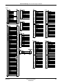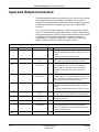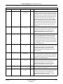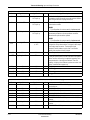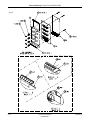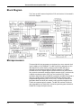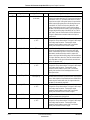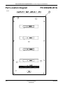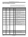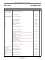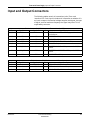
1
Tram-rac 4A Housing Service Manual (Two Board) 2002029-021 127( Due to continuing product innovation, specifications in this manual are subject to change without notice. Trademarks Listed below are GE Medical Systems Information Technologies trademarks. All other trademarks contained herein are the property of their respective owners. 900 SC, ACCUSKETCH, AccuVision, APEX, AQUA-KNOT, ARCHIVIST, Autoseq, BABY MAC, C Qwik Connect, CardioServ, CardioSmart, CardioSys, CardioWindow, CASE, CD TELEMETRY, CENTRA, CHART GUARD, CINE 35, CORO, COROLAN, COROMETRICS, Corometrics Sensor Tip, CRG PLUS, DASH, Digistore, Digital DATAQ, E for M, EAGLE, Event-Link, FMS 101B, FMS 111, HELLIGE, IMAGE STORE, INTELLIMOTION, IQA, LASER SXP, MAC, MAC-LAB, MACTRODE, MANAGED USE, MARQUETTE, MARQUETTE MAC, MARQUETTE MEDICAL SYSTEMS, MARQUETTE UNITY NETWORK, MARS, MAX, MEDITEL, MEI, MEI in the circle logo, MEMOPORT, MEMOPORT C, MINISTORE, MINNOWS, Monarch 8000, MULTI-LINK, MULTISCRIPTOR, MUSE, MUSE CV, Neo-Trak, NEUROSCRIPT, OnlineABG, OXYMONITOR, Pres-R-Cuff, PRESSURE-SCRIBE, QMI, QS, Quantitative Medicine, Quantitative Sentinel, RAC RAMS, RSVP, SAM, SEER, SILVERTRACE, SOLAR, SOLARVIEW, Spectra 400, Spectra-Overview, Spectra-Tel, ST GUARD, TRAM, TRAM-NET, TRAM-RAC, TRAMSCOPE, TRIM KNOB, Trimline, UNION STATION, UNITY logo, UNITY NETWORK, Vari-X, Vari-X Cardiomatic, VariCath, VARIDEX, VAS, and Vision Care Filter are trademarks of GE Medical Systems Information Technologies registered in the United States Patent and Trademark Office. 12SL, 15SL, Access, AccuSpeak, ADVANTAGE, BAM, BODYTRODE, Cardiomatic, CardioSpeak, CD TELEMETRY®-LAN, CENTRALSCOPE, Corolation, EDIC, EK-Pro, Event-Link Cirrus, Event-Link Cumulus, Event-Link Nimbus, HI-RES, ICMMS, IMAGE VAULT, IMPACT.wf, INTER-LEAD, IQA, LIFEWATCH, Managed Use, MARQUETTE PRISM, MARQUETTE® RESPONDER, MENTOR, MicroSmart, MMS, MRT, MUSE CardioWindow, NST PRO, NAUTILUS, O2SENSOR, Octanet, OMRS, PHiRes, Premium, Prism, QUIK CONNECT V, QUICK CONNECT, QT Guard, SMART-PAC, SMARTLOOK, Spiral Lok, Sweetheart, UNITY, Universal, Waterfall, and Walkmom are trademarks of GE Medical Systems Information Technologies. © GE Medical Systems Information Technologies, 2001. All rights reserved. T-2 Tram-rac 4A Housing 2002029-021 Revision A 21 February 2001 1 Introduction . . . . . . . . . . . . . . . . . . . . . . . . . . . . . . . . . . . . 1-1 Manual Information . . . . . . . . . . . . . . . . . . . . . . . . . . . . . . . . . . . . . . . . . . . . . . . . . . 1-3 Revision History . . . . . . . . . . . . . . . . . . . . . . . . . . . . . . . . . . . . . . . . . . . . . . . . . . . 1-3 Manual Purpose . . . . . . . . . . . . . . . . . . . . . . . . . . . . . . . . . . . . . . . . . . . . . . . . . . . 1-3 Related Manuals . . . . . . . . . . . . . . . . . . . . . . . . . . . . . . . . . . . . . . . . . . . . . . . . . . . . 1-4 Tech Memos . . . . . . . . . . . . . . . . . . . . . . . . . . . . . . . . . . . . . . . . . . . . . . . . . . . . . 1-4 Safety Information . . . . . . . . . . . . . . . . . . . . . . . . . . . . . . . . . . . . . . . . . . . . . . . . . . . 1-5 Responsibility of the Manufacturer . . . . . . . . . . . . . . . . . . . . . . . . . . . . . . . . . . . . . 1-5 Intended Use . . . . . . . . . . . . . . . . . . . . . . . . . . . . . . . . . . . . . . . . . . . . . . . . . . . . . 1-5 Definitions of Warnings, Cautions, and Notes . . . . . . . . . . . . . . . . . . . . . . . . . . . . 1-6 Equipment Symbols . . . . . . . . . . . . . . . . . . . . . . . . . . . . . . . . . . . . . . . . . . . . . . . . 1-7 Service Information . . . . . . . . . . . . . . . . . . . . . . . . . . . . . . . . . . . . . . . . . . . . . . . . . . 1-8 Service Requirements . . . . . . . . . . . . . . . . . . . . . . . . . . . . . . . . . . . . . . . . . . . . . . 1-8 Equipment Identification . . . . . . . . . . . . . . . . . . . . . . . . . . . . . . . . . . . . . . . . . . . . . 1-8 Warranty . . . . . . . . . . . . . . . . . . . . . . . . . . . . . . . . . . . . . . . . . . . . . . . . . . . . . . . . 1-8 2 General Information . . . . . . . . . . . . . . . . . . . . . . . . . . . . . 2-1 Equipment Overview . . . . . . . . . . . . . . . . . . . . . . . . . . . . . . . . . . . . . . . . . . . . . . . . . 2-3 Tram-rac Theory . . . . . . . . . . . . . . . . . . . . . . . . . . . . . . . . . . . . . . . . . . . . . . . . . . 2-3 Tram-net Communication . . . . . . . . . . . . . . . . . . . . . . . . . . . . . . . . . . . . . . . . . . . 2-4 Tram-rac 4A Housing . . . . . . . . . . . . . . . . . . . . . . . . . . . . . . . . . . . . . . . . . . . . . . . 2-4 Power Supply Connection . . . . . . . . . . . . . . . . . . . . . . . . . . . . . . . . . . . . . . . . . . 2-12 Technical Specifications . . . . . . . . . . . . . . . . . . . . . . . . . . . . . . . . . . . . . . . . . . . . . 2-13 Revision A Tram-rac 4A 2002029-021 i 3 Maintenance . . . . . . . . . . . . . . . . . . . . . . . . . . . . . . . . . . . 3-1 Controlling Electrostatic Discharge Damage . . . . . . . . . . . . . . . . . . . . . . . . . . . . . 3-3 Guidelines . . . . . . . . . . . . . . . . . . . . . . . . . . . . . . . . . . . . . . . . . . . . . . . . . . . . . . . 3-3 Maintenance Schedule . . . . . . . . . . . . . . . . . . . . . . . . . . . . . . . . . . . . . . . . . . . . . . . 3-4 General . . . . . . . . . . . . . . . . . . . . . . . . . . . . . . . . . . . . . . . . . . . . . . . . . . . . . . . . . 3-4 Inspection . . . . . . . . . . . . . . . . . . . . . . . . . . . . . . . . . . . . . . . . . . . . . . . . . . . . . . . . 3-4 General Cleaning . . . . . . . . . . . . . . . . . . . . . . . . . . . . . . . . . . . . . . . . . . . . . . . . . . 3-5 Electrical Safety Tests . . . . . . . . . . . . . . . . . . . . . . . . . . . . . . . . . . . . . . . . . . . . . . . . 3-6 General . . . . . . . . . . . . . . . . . . . . . . . . . . . . . . . . . . . . . . . . . . . . . . . . . . . . . . . . . 3-6 Recommendations . . . . . . . . . . . . . . . . . . . . . . . . . . . . . . . . . . . . . . . . . . . . . . . . . 3-6 Wall Receptacle Test . . . . . . . . . . . . . . . . . . . . . . . . . . . . . . . . . . . . . . . . . . . . . . . 3-7 Ground (Earth) Integrity . . . . . . . . . . . . . . . . . . . . . . . . . . . . . . . . . . . . . . . . . . . . . 3-7 Ground (Earth) Wire Leakage Current Tests . . . . . . . . . . . . . . . . . . . . . . . . . . . . . 3-8 Enclosure Leakage Current Test . . . . . . . . . . . . . . . . . . . . . . . . . . . . . . . . . . . . . 3-10 Tram-rac 4A Housing Service Kits . . . . . . . . . . . . . . . . . . . . . . . . . . . . . . . . . . . . . 3-12 PN 2006853-001 . . . . . . . . . . . . . . . . . . . . . . . . . . . . . . . . . . . . . . . . . . . . . . . . . 3-12 PN 2006854-001 . . . . . . . . . . . . . . . . . . . . . . . . . . . . . . . . . . . . . . . . . . . . . . . . . 3-12 PN 2006855-001(Repair Kit–3-to-2 Board Conversion) . . . . . . . . . . . . . . . . . . . 3-12 Accessories . . . . . . . . . . . . . . . . . . . . . . . . . . . . . . . . . . . . . . . . . . . . . . . . . . . . . . . 3-13 Repair Log . . . . . . . . . . . . . . . . . . . . . . . . . . . . . . . . . . . . . . . . . . . . . . . . . . . . . . . . 3-14 4 Troubleshooting . . . . . . . . . . . . . . . . . . . . . . . . . . . . . . . . 4-1 Controlling Electrostatic Discharge Damage . . . . . . . . . . . . . . . . . . . . . . . . . . . . . 4-3 Guidelines . . . . . . . . . . . . . . . . . . . . . . . . . . . . . . . . . . . . . . . . . . . . . . . . . . . . . . . 4-3 Wall Receptacle Check . . . . . . . . . . . . . . . . . . . . . . . . . . . . . . . . . . . . . . . . . . . . . . . 4-4 Measure Voltages . . . . . . . . . . . . . . . . . . . . . . . . . . . . . . . . . . . . . . . . . . . . . . . . . 4-4 Ground-Neutral Loop Resistance Check . . . . . . . . . . . . . . . . . . . . . . . . . . . . . . . . 4-4 Check Power Cord . . . . . . . . . . . . . . . . . . . . . . . . . . . . . . . . . . . . . . . . . . . . . . . . . 4-5 General Fault Isolation . . . . . . . . . . . . . . . . . . . . . . . . . . . . . . . . . . . . . . . . . . . . . . . 4-6 First Things to Ask . . . . . . . . . . . . . . . . . . . . . . . . . . . . . . . . . . . . . . . . . . . . . . . . . 4-6 Visual Inspection . . . . . . . . . . . . . . . . . . . . . . . . . . . . . . . . . . . . . . . . . . . . . . . . . . 4-7 Tram-rac 4A LED Troubleshooting Chart . . . . . . . . . . . . . . . . . . . . . . . . . . . . . . . . 4-8 ii Tram-rac 4A 2002029-021 Revision A 5 Tram-rac 4A Housing . . . . . . . . . . . . . . . . . . . . . . . . . . . . 5-1 Theory of Operation . . . . . . . . . . . . . . . . . . . . . . . . . . . . . . . . . . . . . . . . . . . . . . . . . . 5-3 Overview . . . . . . . . . . . . . . . . . . . . . . . . . . . . . . . . . . . . . . . . . . . . . . . . . . . . . . . . 5-3 Top Level Block Diagram . . . . . . . . . . . . . . . . . . . . . . . . . . . . . . . . . . . . . . . . . . . . 5-3 Block Diagram of Control Signals . . . . . . . . . . . . . . . . . . . . . . . . . . . . . . . . . . . . . 5-6 Indicators and Controls . . . . . . . . . . . . . . . . . . . . . . . . . . . . . . . . . . . . . . . . . . . . . . . 5-7 Interconnection Diagram PN 900031 . . . . . . . . . . . . . . . . . . . . . . . . . . . . . . . . . . . . 5-8 Input and Output Connectors . . . . . . . . . . . . . . . . . . . . . . . . . . . . . . . . . . . . . . . . . 5-10 Exploded View PN 900031-005/006 . . . . . . . . . . . . . . . . . . . . . . . . . . . . . . . . . . . . 5-15 Parts List PN 900031-005N/006N . . . . . . . . . . . . . . . . . . . . . . . . . . . . . . . . . . . . . . 5-20 6 Tram-rac 4A Processor Acquisition PCB . . . . . . . . . . . . 6-1 Theory of Operation . . . . . . . . . . . . . . . . . . . . . . . . . . . . . . . . . . . . . . . . . . . . . . . . . . 6-3 Overview . . . . . . . . . . . . . . . . . . . . . . . . . . . . . . . . . . . . . . . . . . . . . . . . . . . . . . . . 6-3 Block Diagram . . . . . . . . . . . . . . . . . . . . . . . . . . . . . . . . . . . . . . . . . . . . . . . . . . . . 6-4 Microprocessors . . . . . . . . . . . . . . . . . . . . . . . . . . . . . . . . . . . . . . . . . . . . . . . . . . . 6-4 Microprocessor Memory . . . . . . . . . . . . . . . . . . . . . . . . . . . . . . . . . . . . . . . . . . . . 6-5 Reset Generator and Watchdog Circuit . . . . . . . . . . . . . . . . . . . . . . . . . . . . . . . . . 6-5 PCB Clock Generation . . . . . . . . . . . . . . . . . . . . . . . . . . . . . . . . . . . . . . . . . . . . . . 6-6 Analog Multiplexers . . . . . . . . . . . . . . . . . . . . . . . . . . . . . . . . . . . . . . . . . . . . . . . . 6-6 Noise Filter and Buffer Amplifier . . . . . . . . . . . . . . . . . . . . . . . . . . . . . . . . . . . . . . 6-6 Analog-to-Digital Converter . . . . . . . . . . . . . . . . . . . . . . . . . . . . . . . . . . . . . . . . . . 6-6 RAC Field Programmable Gate Array (FPGA, U13) . . . . . . . . . . . . . . . . . . . . . . . 6-7 Indicators and Controls . . . . . . . . . . . . . . . . . . . . . . . . . . . . . . . . . . . . . . . . . . . . . . 6-10 Input and Output Connectors . . . . . . . . . . . . . . . . . . . . . . . . . . . . . . . . . . . . . . . . . 6-11 Module Interface (J1–J4) . . . . . . . . . . . . . . . . . . . . . . . . . . . . . . . . . . . . . . . . . . . 6-11 Interface PCB (J5) . . . . . . . . . . . . . . . . . . . . . . . . . . . . . . . . . . . . . . . . . . . . . . . . 6-14 ISP Serial EEPROM Interface (J6) . . . . . . . . . . . . . . . . . . . . . . . . . . . . . . . . . . . 6-15 Part Location Diagram PN 2004288-001A. . . . . . . . . . . . . . . . . . . . . . . . . . . . . . . . 6-16 Parts List PN 2004288-001A . . . . . . . . . . . . . . . . . . . . . . . . . . . . . . . . . . . . . . . . . . 6-19 Schematic Diagram PN 2004289-001A . . . . . . . . . . . . . . . . . . . . . . . . . . . . . . . . . . 6-21 Revision A Tram-rac 4A 2002029-021 iii 7 Tram-rac 4A Interface PCB . . . . . . . . . . . . . . . . . . . . . . . . 7-1 Theory of Operation . . . . . . . . . . . . . . . . . . . . . . . . . . . . . . . . . . . . . . . . . . . . . . . . . 7-3 Overview . . . . . . . . . . . . . . . . . . . . . . . . . . . . . . . . . . . . . . . . . . . . . . . . . . . . . . . . 7-3 Block Diagram . . . . . . . . . . . . . . . . . . . . . . . . . . . . . . . . . . . . . . . . . . . . . . . . . . . . 7-3 Indicators and Controls . . . . . . . . . . . . . . . . . . . . . . . . . . . . . . . . . . . . . . . . . . . . . . 7-8 Input and Output Connectors . . . . . . . . . . . . . . . . . . . . . . . . . . . . . . . . . . . . . . . . . . 7-9 Part Location Diagram PN 800516-001J/002J . . . . . . . . . . . . . . . . . . . . . . . . . . . . 7-13 Parts List PN 800516-001 . . . . . . . . . . . . . . . . . . . . . . . . . . . . . . . . . . . . . . . . . . . . 7-14 Parts List PN 800516-002 . . . . . . . . . . . . . . . . . . . . . . . . . . . . . . . . . . . . . . . . . . . . 7-16 Schematic Diagram PN SD800516-001D . . . . . . . . . . . . . . . . . . . . . . . . . . . . . . . . 7-18 8 Tram-rac 4A Power Supply . . . . . . . . . . . . . . . . . . . . . . . 8-1 Theory of Operation . . . . . . . . . . . . . . . . . . . . . . . . . . . . . . . . . . . . . . . . . . . . . . . . . 8-3 Overview . . . . . . . . . . . . . . . . . . . . . . . . . . . . . . . . . . . . . . . . . . . . . . . . . . . . . . . . 8-3 Indicators and Controls . . . . . . . . . . . . . . . . . . . . . . . . . . . . . . . . . . . . . . . . . . . . . . 8-4 Input and Output Connectors . . . . . . . . . . . . . . . . . . . . . . . . . . . . . . . . . . . . . . . . . . 8-5 Part Location Diagram PN 6123-211A. . . . . . . . . . . . . . . . . . . . . . . . . . . . . . . . . . . . 8-6 Parts List PN 6123-211A . . . . . . . . . . . . . . . . . . . . . . . . . . . . . . . . . . . . . . . . . . . . . . 8-7 Schematic DiagramPN SD6123-211A . . . . . . . . . . . . . . . . . . . . . . . . . . . . . . . . . . . 8-10 iv Tram-rac 4A 2002029-021 Revision A 1 Revision A Introduction TRAM-RAC 4A 2002029-021 1-1 For your notes 1-2 TRAM-RAC 4A 2002029-021 Revision A Introduction: Manual Information Manual Information Revision History Each page of the document has the document part number and revision letter at the bottom of the page. The revision letter changes whenever the document is updated. Table 1. Revision History Revision Date A 23 February 2001 Comment Initial release of this manual for the Tram-rac 4A Two Board version. Manual Purpose Silver or gold? This manual supplies technical information for service representative and technical personnel so they may maintain the equipment to the assembly level. Use it as a guide for maintenance and electrical repair considered field repairable. n This manual applies only to the Tram-rac 4A with the silver plate below the module slots. (Two Board version) n The Tram-rac Housing Service Manual (PN404183-096) is for Tram-rac 4A housings with the gold plate below the module slots. (Three Board version) A service kit is available to repair existing Tram-rac 4As with the gold plate. See “Tram-rac 4A Housing Service Kits” on page 3-12 for the available kit. Users of this manual are expected to have a strong background in electronics, including analog and digital circuity with microprocessor and micro-controller architecture. Revision A TRAM-RAC 4A 2002029-021 1-3 Introduction: Related Manuals Related Manuals Check these documents if you need additional information about related producets. Table 2. Service Documents Part Number Name 404183-006 Tram-rac Chassis Service Manual (For Tram-rac 3 and Tram-rac 4 Housing) 404183-048 Tramscope 12C Monitor Service Manual 404183-094 Tramscope 12 Monitor Service Manual 404183-096 Tram-rac Housing Service Manual 404183-150 Modular Patient Monitor Accessories Manual 404422-001 Tram 100-600 Modules Service Manual 404422-065 Tram 100-850 A & SL Modules Service Manual 405040-002 Centralscope 12 Central Station Service Manual 405040-018 Centralscope 12C Central Station Service Manual 405040-117 Modular Centralscope Central Station Service Manual 414993-001 Solar 7000/8000/View Patient Monitor Service Manual 414993-007 Solar 7000 Patient Monitor Data Manual 2000701-001 Solar 8000M Patient Monitor Service Manual 421669-001 Solar 9500 Information Monitor Service Manual Table 3. Operator Documents Name Tram Critical Care Monitor Operator’s Manual Centralscope Central Station and CD Telemetry–LAN Monitoring System Operator's Manual Solar 7000/8000 Patient Monitor Operator’s Manual Solar 8000M Patient Monitor Operator's Manual Solar 9500 Information Monitor Operator’s Manual Tech Memos GE Medical Systems Information Technologies Service issues technical memos that aid service personnel in servicing and maintaining the equipment. Tech Memos supply important information about changes to the equipment, typical problems, and how to solve those problems. Tech Memos are also written to describe hardware and software upgrades. Tech Memos are automatically distributed to all GE Medical Systems Information Technologies Field Service personnel, and are available to customers by subscription. Contact Technical Support for more information or to subscribe. For the address or telephone number, see How to Reach Us...”.“ 1-4 TRAM-RAC 4A 2002029-021 Revision A Introduction: Safety Information Safety Information Responsibility of the Manufacturer GE Medical Systems Information Technologies is responsible for the effects of safety, reliability, and performance only if: n Assembly operations, extensions, readjustments, modifications, or repairs are carried out by persons authorized by Information Technologies. n The electrical installation of the relevant room complies with the requirements of the appropriate regulations. n The equipment is used in accordance with the instructions for use. Intended Use This device is intended for use under the direct supervision of a licensed health care practitioner. To ensure patient safety, use only parts and accessories manufactured or recommended by GE Medical Systems Information Technologies. Contact Information Technologies for information before connecting any devices to this equipment that are not recommended in this manual. Revision A TRAM-RAC 4A 2002029-021 1-5 Introduction: Safety Information Definitions of Warnings, Cautions, and Notes Warnings, cautions, and notes are used throughout this manual to designate a degree or level of hazardous situations. Hazard is defined as a source of potential injury to a person. '$1*(5 indicates an imminent hazard which, if not avoided, will result in death or serious injury. :$51,1* indicates a potential hazard or unsafe practice which, if not avoided, could result in death or serious injury. &$87,21 indicates a potential hazard or unsafe practice which, if not avoided, could result in minor personal injury or product/property damage. 127(provides application tips or other useful information to assure that you get the most from your equipment. 1-6 TRAM-RAC 4A 2002029-021 Revision A Introduction: Safety Information Equipment Symbols The following symbols appear on the equipment. 127( Some symbols may not appear on all equipment. ATTENTION: Consult accompanying documents before using the equipment. In Europe, this symbol means dangerous or high voltage. In the United States, this symbol represents the caution notice below: To reduce the risk of electric shock, do NOT remove cover (or back). Refer servicing to qualified personnel. Defibrillator-proof type CF equipment; type CF equipment is specifically designed for applications where a conductive connection directly to the heart is established. The paddles indicate the equipment is defibrillator proof. Defibrillator-proof type BF equipment; type BF equipment is specifically designed for applications intentional external and internal application to the patient, excluding direct cardiac application. Type BF equipment is type B equipment with an F-type isolated (floating) part. The paddles indicate the equipment is defibrillator proof. Type B equipment; type B equipment is suitable for intentional external and internal application to the patient, excluding direct cardiac application. Equipotentiality Alternating current (AC) Power; , = ON; 2 = OFF Fuse PRESS Indicates where to press to open the door on the Series 7160 Direct Digital Writer. Revision A TRAM-RAC 4A 2002029-021 1-7 Introduction: Service Information Service Information Service Requirements Follow the service requirements listed below. n Refer equipment servicing to GE Medical Systems Information Technologies’ authorized service personnel only. n Any unauthorized attempt to repair equipment under warranty voids that warranty. n It is the user’s responsibility to report the need for service to GE Medical Systems Information Technologies or to one of their authorized agents. n Failure on the part of the responsible individual, hospital, or institution using this equipment to implement a satisfactory maintenance schedule may cause undue equipment failure and possible health hazards. n Regular maintenance, irrespective of usage, is essential to ensure that the equipment will always be functional when required. Equipment Identification Every GE Medical Systems Information Technologies device has a unique serial number for identification. The serial number appears on the product label on the base of each unit under the Trim knob control. D 1 XX 0005 G XX Month Manufactured A = January B = February C = March D = April E = May F = June G = July H = August J = September K = October L = November M = December Year Manufactured 1 = 2001 2 = 2002 3 = 2003 (and so on) Product Code Two-character product descriptor ST = Tram-rac 4A Product Sequence Number Division Manufacturing F = Diagnostic number (of total G = Monitoring units N = Freiburg manufactured.) Hellige Device Characteristics One or 2 letters that further describe the unit, for example: P = prototype not conforming to marketing specification R = refurbished equipment S = special product documented under Specials part numbers U = upgraded unit Warranty 1 year. 1-8 TRAM-RAC 4A 2002029-021 Revision A 2 Revision A General Information Tram-rac 4A Housing 2002029-021 2-1 For your notes 2-2 Tram-rac 4A Housing 2002029-021 Revision A General Information: Equipment Overview Equipment Overview Tram-rac Theory The Tram-rac housing (remote acquisition case) acquires the patient data for the patient monitor. It provides an interface between the patient monitor and a Tram module or discrete parameter module. An interface cable provides the communications media between the Tram-rac 4A and the host monitor. If the Tram-rac 4A is an unpowered RAC (pn 900031-005), the cable provides +16.5V power. If a Tram-rac housing is located more than 20 feet from the patient monitor, the Tram-rac housing needs its own power supply. 127( For an equipment overview of other products used in the Tram Critical Care Monitoring system, refer to Table 2, “Service Documents,” on page 1-4. Communication options and Tram-net communication are explained in “Tram-net Communication” on page 2-4. There are three Tram-rac housings available for the patient monitor: n Tram-rac 2 housing, which houses a single Tram module or two discrete modules, n Tram-rac 2A housing, which houses a single Tram module or two discrete modules, n Tram-rac 4A housing, which houses a Tram module and two discrete parameter modules or no Tram module and four discrete parameter modules. 127( If your system contains a Tram-rac 4 (not 4A) housing, it houses only two discrete parameter modules and a Tram module in the top slot. This manual addresses only the Tram-rac 4A. Revision A Tram-rac 4A Housing 2002029-021 2-3 General Information: Equipment Overview Tram-net Communication Tram-net communication permits connection to the Tram-rac housing and other bedside peripherals. The Tram-net communication is one form of local area network that provides a data and power link from the monitor to peripheral devices. The connector makes a communication processor available for the peripheral devices. The Tram-net controller processor is built into the communication PCB assembly which frees up the main processor in the monitor. To avoid confusion, consider Tram-net communication as a small area network (SAN) contained in one room or at the patient bedside. For more details about communication networks, refer to the appropriate monitor service manual. Tram-rac 4A Housing Shown below is a Tram-rac 4A housing with a Tram module and one BP and one BP/Dual Temperature module inserted. The Tram-rac 4A housing has three communication connectors: n n The 15-pin yellow color-coded connector is used for analog output, The two 9-pin blue color-coded connectors are for: u u u u Tram-net communication with a patient monitor, Tram-net hub, remote control, or an additional Tram-rac housing. The number of peripheral devices is dependent upon the software version of the host monitor. When you use an optional power supply, there is an additional hidden connector on the back panel for the power supply connection. 2-4 Tram-rac 4A Housing 2002029-021 Revision A General Information: Equipment Overview Below are examples of the rear label of the Tram-rac 4A housing with and without a power supply. Further explanation about connection and labeling of the male and female Tram-net connectors is found on the following pages. ANALOG OUT TRAM NET TRAM NET ANALOG OUT TRAM-RAC Ports TRAM NET TRAM NET TRAM NET TRAM-RAC Ports TRAM NET TRAM NET TRAM NET 50-60 Hz CAUTION Tram-rac without Power Supply Revision A V~ I 100–120V 1A 220–240V 500mA Tram-rac with Power Supply Tram-rac 4A Housing 2002029-021 2-5 General Information: Equipment Overview Solar 7000/8000 Monitor Connection The Solar patient monitor can support two Tram-rac housings. The right Tram-net connector may be connected to the following: n n n a monitor, a Tram-net hub, or another Tram-rac housing if this Tram-rac housing has a power supply. The center Tram-net connector may be connected to the following: n n a remote control or to another Tram-rac 4A housing with a power supply. 127( The Tram-rac housing furthest from the monitor must have a power supply. Shown below are examples of how to connect dual Tram-rac housing to a Solar 7000 or 8000 monitor. Note that the Solar 8000 has a horizontal orientation. C RMT ALM ASYNC COMM ANALOG OUT TRAM NET TRAM NET ANALOG OUT TRAM-NET ETHERNET TRAM-RAC Ports TRAM NET TRAM NET TRAM NET TRAM-RAC Ports TRAM NET TRAM NET TRAM NET RS-232 RMT VID A 50-60 Hz CAUTION 1. I 1A 220–240V 500mA ASYNC COMM 2. 3. V~ 100–120V 4. B C RMT ALM ASYNC COMM D ANALOG OUT TRAM NET TRAM NET TRAM-NET ETHERNET RMT VID RS-232 TRAM-RAC Ports TRAM NET ANALOG OUT TRAM NET TRAM NET TRAM-RAC Ports TRAM NET TRAM NET TRAM NET 50-60 Hz CAUTION V~ I 100–120V 1A 220–240V 500mA See “Accessories” on page 3-13 for cables and cable part numbers. 2-6 Tram-rac 4A Housing 2002029-021 Revision A General Information: Equipment Overview Solar 8000M Monitor Connection The Solar patient monitor can support two Tram-rac housings. The right Tram-net connector may be connected to the following: n n n a monitor, a Tram-net hub, or another Tram-rac housing if this Tram-rac housing has a power supply. The center Tram-net connector may be connected to the following: n n a remote control or to another Tram-rac 4A housing with a power supply. 127( The Tram-rac housing furthest from the monitor must have a power supply. See below to connect dual Tram-rac housing to a Solar 8000M monitor C A A A See “Accessories” on page 3-13 for cables and cable part numbers. :$51,1* Equipment damage. Connect the Octanet and Tram-rac housing to the Solar 8000M patient monitor BEFORE plugging the power cord into an AC outlet. Connecting these devices to a powered Solar 8000M patient monitor could damage the connectors. Revision A Tram-rac 4A Housing 2002029-021 2-7 General Information: Equipment Overview Tramscope Monitor Connection The level of software used in the connected patient monitor determines how the two Tram-net connectors on the Tram-rac 4A may be used. Tramscope V6/V7 Software If your Tramscope monitor uses V6 or V7 software, the monitor may only support one Tram-rac housing. The right Tram-net connector may be connected to the following: n n the monitor or a Tram-net hub. The center Tram-net connector may be connected a remote control but NOT to another Tram-rac housing. 1. ASYNC 2. 3. COMM B 4. ETHERNET ASYNC COMM D ANALOG TRAM TRAM OUT NET NET TRAM-RAC Ports TRAM TRAM NET NET TRAM-NET OR ASYNC COMM ETHERNET ANALOG TRAM TRAM OUT NET NET ASYNC COMM TRAM-RAC Ports TRAM TRAM NET NET TRAM-NET OR ASYNC COMM A See “Accessories” on page 3-13 for cables and cable part numbers. 2-8 Tram-rac 4A Housing 2002029-021 Revision A General Information: Equipment Overview Tramscope V17 Software If your Tramscope monitor uses V17 software, the monitor may support two Tram-rac housings. The right Tram-net connector may be connected to the following: n n n a monitor, a Tram-net hub, or another Tram-rac housing if this Tram-rac housing has a power supply. The center Tram-net connector may be connected to the following: n n a remote control or to another Tram-rac 4A housing with a power supply. 127( The Tram-rac housing furthest from the monitor must have a power supply. If older models of Tram-rac housing are used, a Tram-net hub is necessary. Shown below are examples of how to connect dual Tram-rac housing to a monitor. C ETHERNET ANALOG TRAM TRAM OUT NET NET ANALOG TRAM TRAM OUT NET NET ASYNC COMM TRAM-RAC Ports TRAM-RAC Ports TRAM TRAM NET NET TRAM TRAM NET NET TRAM-NET OR ASYNC A CAUTION 50-60 Hz COMM 1. I 1A 220240V 500mA ASYNC COMM 2. 3. V~ 100120V B 4. C ETHERNET ANALOG OUT ASYNC COMM D TRAM NET TRAM NET TRAM-RAC Ports TRAM NET ANALOG OUT TRAM NET TRAM NET TRAM-RAC Ports TRAM NET TRAM NET TRAM NET TRAM-NET OR ASYNC COMM 50-60 Hz CAUTION V~ I 100–120V 1A 220–240V 500mA See “Accessories” on page 3-13 for cables and cable part numbers. Revision A Tram-rac 4A Housing 2002029-021 2-9 General Information: Equipment Overview Analog Output Connection The analog out connector is provided for customized uses for other peripheral devices. The yellow color-coded 15-pin connector provides an analog output waveform signal. 15 14 13 12 11 10 9 8 7 6 5 4 3 2 1 Note the parameter numbers indicated on the front of the Tram-rac 4A housing. TRAM 2-10 RAC4A 1 2 3 4 5 6 7 8 Tram-rac 4A Housing 2002029-021 Revision A General Information: Equipment Overview When a Tram or discrete parameter module is inserted into the housing, the slot number of the parameter and its analog output waveform is available at a designated pin of the analog out connector. Refer to the list below 127( The Tram module must be in the top slot in order to receive the Tram signals listed below. Table 1. Analog Output Signals Analog Output Pin Signal Name Bezel Number For BP Pin 1 Signal Ground for Tram Waveforms – Pin 2 Trace 1 Tram1 Pin 3 Tram BP3 or SPO2 Value Tram1 Pin 42 Slot 1 Discrete Module Waveform A Pin 5 Tram ART 1 or BP1 Pin 6 Slot 3 Discrete Module Waveform A 6 Pin 7 Slot 4 Discrete Module Waveform A 8 Pin 8 Signal Ground for Discrete Module Waveforms Pin 9 Tram ECG II Tram1 Pin 10 Tram ECG V Tram1 Pin 11 Tram BP4 or RESP Tram1 Pin 122 Slot 1 Discrete Module Waveform B Pin 13 Tram BP2 or SPO2 Waveform Pin 14 Slot 3 Discrete Module Waveform B 5 Pin 15 Slot 4 Discrete Module Waveform B 7 1 Tram 2 Tram 127( The superscript number 1 indicates that this signal remains unchanged after entering the Tram-rac 4A housing and is controlled by Tram module software. All other signals are generated by the DAC (digital-to-analog converter) on the Tram-rac 4 interface PCB assembly. The asterisk indicates reserved for future use. Revision A Tram-rac 4A Housing 2002029-021 2-11 General Information: Equipment Overview Power Supply Connection The power supply is required where one or more of the following conditions apply: 2-12 n n The Tram-rac 4A is more the 20 feet from the monitor, n One Tram-rac without a power supply is already connected to the monitor (or Tram-net hub), or n You exceeded the monitor power supply capability. The Tram-rac 4A operates in an environment with high electrical noise, Tram-rac 4A Housing 2002029-021 Revision A General Information: Technical Specifications Technical Specifications Table 2. Performance Specifications for Analog Output Item Description ECG (From Tram or Discrete Parameter Module) Trace I and II gain 1 V/mV ±10% Range ±5 mV Frequency response 0.05 Hz to 100 Hz Respiration (From Tram module only) Lead Displayed lead Gain 1 V/ohm Range 0.4 ohm to 10 ohms Frequency response 0.05 Hz to 2.2 Hz Outputs Tram: Arterial BP, BP 2, BP 3, BP 4 Discrete Parameter Module: Up to 3 additional BP signals for slots 5, 6 and 8 (Dependent on Tram-rac housing size.) Gain 10 mV/mm Hg ±5% Frequency response 0 to 50 Hz Range -25 mm Hg to 300 mm Hg; 0 mm Hg = 0.0V ±0.005V Blood Pressure (From Tram or Discrete Parameter Module) Table 3. Communication Specifications Item Description Communications to monitor provided by Tram-net communication Data acquisition Intel 80C31, 8-bit, 14.7 MHz Communication to display Intel 80C152, 8-bit, 14.7 MHz Revision A Tram-rac 4A Housing 2002029-021 2-13 General Information: Technical Specifications Table 4. Environmental Specifications Item Description Tram-rac housing 4A with power supply Power requirements 220 ±40 VAC, 50/60 Hz, single phase Power consumption 120 watts Low voltage shutdown 90 VAC/180 VAC Cooling Convection Heat dissipation 238 Btu/hr (70 watts) Tram-rac housing 4A without power supply Maximum distance from monitor 3.67 m (20 ft) Power requirements from monitor 16.5 V @ 3.5 A Tram-rac housing (All) Operation conditions n Ambient temperature n Relative humidity 10° C to 35° C (50° F to 95° F) 40% to 95% (noncondensing) Storage conditions n Temperature n Relative humidity –10° C to 50° C (14° F to 122° F) 0% to 95% (noncondensing) Table 5. Physical Specifications Item Height Description 22.9 cm (9.0 in) Width 14.5 cm (5.7 in) Depth 33.5 cm (13.2 in) Depth w/ power supply 38.4 cm (15.1 in) Weight 2.9 kg (6.4 lb) Weight w/power supply 3.5 kg (7.9 lb) Table 6. Certification Item Safety standards 2-14 Description UL544 listed, IEC 601 certified Meets current ANSI/AAMI safety and performance standards Complies with CSA No. 125 Tram-rac 4A Housing 2002029-021 Revision A 3 Revision A Maintenance Tram-rac 4A Housing 2002029-021 3-1 For your notes 3-2 Tram-rac 4A Housing 2002029-021 Revision A Maintenance: Controlling Electrostatic Discharge Damage Controlling Electrostatic Discharge Damage All components of the Tram Critical Care Monitoring System make extensive use of CMOS components. CMOS components are used because they are more immune to noise and consume less power than standard TTL or NMOS components. However, by their nature CMOS components are more vulnerable to electrostatic discharge (ESD) damage than other semiconductors. ESD damage, usually a subtle weakening of semiconductor junctions, can range from corruption of digital memory to catastrophic failure, rendering a component or a number of components permanently unusable. Although it is more common for CMOS components to fail from ESD damage, no semiconductor device is completely safe from ESD damage. The inputs and outputs of all of the components are protected from ESD damage, so they are no more susceptible to ESD damage during normal operation than any other device. However, when you service components, you expose the components to several sources of static electricity, ranging from human hands to improperly grounded test equipment. For this reason, it is recommended that all service workstations be as staticfree as possible. Guidelines The following guidelines can help make your workstation more resistant to the damage that can be caused by static electricity. Revision A n Discharge any static charge you may have built up before handling semiconductors or assemblies containing semiconductors. n A grounded, antistatic wristband or heelstrap should be worn at all times when repairing assemblies containing semiconductors. n n Use only properly grounded soldering and test equipment. n Do NOT remove semiconductors or assemblies containing semiconductors from antistatic containers (bags) until needed. n Make sure power to an assembly is turned off before removing or inserting a semiconductor. n Do NOT slide semiconductors or assemblies containing semiconductors across any surface. n n Do NOT touch semiconductor leads unless absolutely necessary. Use a static-free surface when working on assemblies containing semiconductors. Semiconductors and assemblies containing semiconductors should be stored only in antistatic bags or boxes. Tram-rac 4A Housing 2002029-021 3-3 Maintenance: Maintenance Schedule Maintenance Schedule General An effective maintenance schedule should be established for the Tramrac 4A. The schedule should include inspection, general cleaning, performance testing, and safety testing on a regular basis. Safety tests are recommended to be performed every twelve months or if any internal components have been altered. :$51,1* A failure, on the part of the responsible individual hospital or institution employing the uses of this monitoring equipment, to implement a satisfactory maintenance schedule may cause undue equipment failure and possible health hazards. Inspection Inspect the Tram-rac 4A on a regular basis. Follow these guideline when you inspect the equipment. n Inspect the equipment for obvious physical damage and replace damaged items. n Inspect all connectors for bent pins or prongs. Replace or repair any bad cables or connectors. 127( Only qualified service personnel should replace the connectors. 3-4 n Inspect all cable insulation. Qualified service personnel should repair or replace damaged or deteriorated cables. n Inspect fuses. Tram-rac 4A Housing 2002029-021 Revision A Maintenance: Maintenance Schedule General Cleaning Exterior Cleaning Clean the Respiratory Mechanics Module on a regular basis. Clean the exterior surfaces of the device with a dampened lint-free cloth. Use one of the following approved solutions: n n n n ammonia (diluted), Cidex, sodium hypochlorite bleach (diluted), or mild soap (diluted). To avoid damage to the equipment, follow these rules. &$87,21 Failure to follow these rules may melt, distort, or dull the finish of the case, blur lettering on the labels, or cause equipment failures. Always dilute the solutions according to the manufacturer’s suggestions. Always wipe off all the cleaning solutions with a dry cloth after cleaning. Never use wax containing a cleaning substance. Never pour water or any cleaning solution on the equipment or permit fluids to run behind switches, into the connectors, or into any ventilation openings in the equipment. Never use these cleaning agents: n n n abrasive cleaners or solvents of any kind, n Betadine. acetone, alcohol based cleaning agents (except for cleaning the thermal print head), or Interior Cleaning On a regular basis, qualified service personnel should open the RM-M or RM module and blow dust from unit with compressed air. Revision A Tram-rac 4A Housing 2002029-021 3-5 Maintenance: Electrical Safety Tests Electrical Safety Tests General Electrical safety tests provide a method of determining if potential electrical health hazards to the patient or operator of the device exist. These tests are for Tram-rac 4A units with the optional power supply. If your Tram-rac 4A does NOT have a power supply, see the test procedure in the service manual of the host monitor( i.e., Solar 8000, Solar 9500, etc.). Recommendations GE Medical Systems Information Technologies recommends electrical safety tests be performed: n n n upon receipt of the module, n To safety test a Tram-rac 4A without a power supply, leave it connected to a monitor during the safety tests. n Safety test a Tram-rac 4A with a power supply separately. every twelve months thereafter, and each time the module is opened or repaired. Record the date and results on the “Repair Log” on page 3-14 ( at the end of this chapter). Required Tests These instructions are intended for for Tram-rac 4A units with the optional power supply. Listed below are the safety tests. n n n n Wall receptacle test, Ground (Earth) integrity, Ground (Earth) leakage current tests, and Enclosure leakage current tests. Checkout procedures, safety tests, and leakage tests are described in the “Maintenance” chapter of the appropriate patient monitor. See Table 2, “Service Documents,” on page 1-4 for the appropriate manual. 127( Perform the safety tests for the Tram modules or discrete parameter modules used in the Tram-rac 4A according to the directions in their respective service manuals. If a Tram-rac 4A under test fails the leakage tests, call Tech Support for assistance. (See “How to Reach Us.”) 3-6 Tram-rac 4A Housing 2002029-021 Revision A Maintenance: Electrical Safety Tests Test Conditions All electrical safety tests may be performed under normal ambient temperature, humidity, and pressure conditions. Test Equipment A Leakage Current Tester is needed. Wall Receptacle Test Before starting the tests, the wall receptacle from which the device will get electrical power must be checked. This test checks the condition of the wall receptacle to ensure correct results from leakage tests. For international wall receptacles, refer to the internal standards agencies of that particular country. Use a digital multimeter to ensure the wall receptacle is wired properly. If other than normal polarity and ground is indicated, corrective action must be taken before proceeding. The results of the following tests will be meaningless unless a properly wired wall receptacle is used. Ground (Earth) Integrity Ground Pin Listed below are two methods for checking the ground (earth) integrity, “Ground Continuity Test” and “Impedance of Protective Earth Connection.” These tests determine whether the device’s exposed metal and power inlet’s earth (ground) connection has a power ground fault condition. Perform the test method below that is required by your Country/Local governing safety organization. Ground Continuity Test Completion of this test is checked by the following steps: 1. Disconnect the DUT (device under test) from the wall receptacle. 2. Connect the negative(–) lead of the ohm meter to the protective earth terminal (ground pin in power in-let connector) or the protective earth pin in the MAINS PLUG (ground pin in power cord). Refer to the US 120Vac power cord figure on the left. 3. Set the Ohm meter to the milliohm (mΩ) range. 4. Connect the positive (+) lead of the Ohm meter to all exposed metal surfaces on the DUT. If the metal surfaces are anodized or painted scrape off a small area in a inconspicuous area for the probe to make contact with the metal. Revision A Tram-rac 4A Housing 2002029-021 3-7 Maintenance: Electrical Safety Tests 5. Resistance should read to pass: u 0.1 ohm or less without power cord u 0.2 ohms or less with power cord Impedance of Protective Earth Connection This test unlike a ground continuity test will also stress the ground system by using special ground bond testers i.e. Kikusui (model 872 or TOS 6100) or Associated Research model HYAMP® Jr. Model 3030D. This test normally is only required as a manufacturing production test to receive safety agency compliance (i.e. IEC601-1). Some country agency’s do require this test after field equipment repairs (i.e. Germany's DIN VDE 0751 standards). Consult your country/local safety agency if in question. Compliance is checked by the following steps: 1. A current not less than 10A and not exceeding 25 A from a current source with a frequency of 50 or 60 Hz with a no-load voltage not exceeding 6 V is passed for at least 5 s through the PROTECTIVE EARTH TERMINAL or the protective earth pin in the MAINS PLUG and each ACCESSIBLE METAL PART which could become LIVE in case of failure in BASIC INSULATION. 2. The voltage drop between the parts described is measured and the impedance determined from the current and voltage drop. It shall not exceed the values indicated. For EQUIPMENT without a POWER SUPPLY CORD the impedance between the PROTECTIVE EARTH TERMINAL and any ACCESSIBLE METAL PART which is PROTECTIVELY EARTHED shall not exceed 0.1 ohms For EQUIPMENT with a POWER SUPPLY CORD the impedance between the protective earth pin in the MAINS PLUG and any ACCESSIBLE METAL PART which is PROTECTIVELY EARTHED shall not exceed 0.2 ohms. When taking this measurement move the customer’s power cord around, no fluctuations in resistance should be observed. Ground (Earth) Wire Leakage Current Tests Perform this test to measure current leakage through the ground (earth) wire of the equipment during normal operation. 1. Set the leakage tester switches as follows: u GND switch - OPEN, u Polarity switch - NORM, u Power switch - OFF. 3-8 Tram-rac 4A Housing 2002029-021 Revision A Maintenance: Electrical Safety Tests 2. Connect the DMM to the METER jacks on the leakage tester. Set the DMM to measure AC millivolts. 3. Connect the power cord of the device under test to the power receptacle on the rear of the leakage tester. 127( The device under test is to be tested at its normal operating voltage. 4. Set the leakage tester power switch to ON. 5. Set the power switch of the device under test to ON. 6. Read the current leakage indicated on DMM. If the reading is greater than the appropriate specification below, the device under test fails and should be repaired and tested again. u 300 µA (0.3 volts on the DMM), and the device under test is powered from 100-120 V/50-60 Hz u 300 µA (0.3 volts on the DMM), and the device under test is powered from a centered-tapped 200-240 V/50-60 Hz, single phase circuit u 500 µA (0.5 volts on the DMM), and the device under test is powered from a non-center-tapped, 200-240 V/50-60 Hz, singlephase circuit 127( Center-tapped and non-center-tapped circuits produce different leakage currents and the UL and IEC limits are different. 7. Set the polarity switch on the leakage tester to RVS (reverse). 8. Read the current leakage indicated on DMM. If the reading is greater than the appropriate specification below, the device under test fails and should be repaired and tested again. u 300 µA (0.3 volts on the DMM), and the device under test is powered from 100-120 V/50-60 Hz u 300 µA (0.3 volts on the DMM), and the device under test is powered from a centered-tapped 200-240 V/50-60 Hz, single phase circuit u 500 µA (0.5 volts on the DMM), and the device under test is powered from a non-center-tapped, 200-240 V/50-60 Hz, singlephase circuit Center-tapped and non-center-tapped circuits produce different leakage currents and the UL and IEC limits are different. Revision A Tram-rac 4A Housing 2002029-021 3-9 Maintenance: Electrical Safety Tests 9. Set the leakage tester power switch to OFF. 127( The MD (measuring device) is the circuitry defined by the appropriate standard for measuring leakage current. The measuring devices, defined by various standard organizations (IEC, UL, etc.), produce almost identical test measurement results. Enclosure Leakage Current Test Perform this test to measure current leakage through exposed conductive surfaces on the device under test during normal operation. 1. Set the leakage tester switches as follows: u GND switch - OPEN, u Polarity switch - NORM. 2. Connect a meter lead between the CHAS connector on the rear of the leakage tester and an unpainted, non-anodized chassis ground on the unit under test. 3. Set the leakage tester power switch to ON. 4. Read the current leakage indicated on DMM. If the reading is greater than the appropriate specification below, the device under test fails and should be repaired and tested again. u 300 µA (0.3 volts on the DMM), and the device under test is powered from 100-120 V/50-60 Hz u 300 µA (0.3 volts on the DMM), and the device under test is powered from a centered-tapped 200-240 V/50-60 Hz, single phase circuit u 500 µA (0.5 volts on the DMM), and the device under test is powered from a non-center-tapped, 200-240 V/50-60 Hz, singlephase circuit 127( Center-tapped and non-center-tapped circuits produce different leakage currents and the UL and IEC limits are different. 3-10 Tram-rac 4A Housing 2002029-021 Revision A Maintenance: Electrical Safety Tests 5. Set the polarity switch to RVS and observe the same meter readings as in the previous step. 6. Set the GND switch on the leakage tester to CLOSED. 7. Read the current leakage indicated on DMM. If the reading is greater than the appropriate specification below, and the device under test is powered from 100-240 V/50-60 Hz, the device under test fails and should be repaired and tested again. u 100 microamperes (0.1 volts on the DMM), and the device under test is powered from 100-240 V/50-60 Hz 8. Set the polarity switch to RVS and observe the same meter readings as in the previous step. 9. Set the leakage tester power switch to OFF and remove the meter lead connected in step 2. Revision A Tram-rac 4A Housing 2002029-021 3-11 Maintenance: Tram-rac 4A Housing Service Kits Tram-rac 4A Housing Service Kits The following part lists are given for ordering purposes. These kits are available to aid troubleshooting by swapping a suspect component. 127( When ordering these kits, note that each kit contains only the latest revision of the PCB assemblies. Contact Service—Tech Support to verify if the latest revision is compatible with your system. PN 2006853-001 This kit can be ordered as an aid to troubleshooting a Tram-rac 4A chassis without a power supply. Table 7. Tram-rac 4A Service Kit Part Number Qty Tram-rac4A Processor Acquisition PCB Description 2004288-001 1 Tram-rac4A Interface PCB 800516-001 1 PN 2006854-001 This kit can be ordered as an aid to troubleshooting a Tram-rac 4A chassis with a power supply. Table 8. Tram-rac 4A w/Power Supply Service Kit Description Part Number Qty Tram-rac4A Processor Acquisition PCB 2004288-001 1 Tram-rac4A Interface PCB 800516-002 1 Tram-rac 4A Power Supply 6123-211 1 PN 2006855-001(Repair Kit–3-to-2 Board Conversion) This kit can be ordered to repair an older Tram-rac 4A (with the gold plate below the module slots). Use this kit to repair an older Tram-rac 4A if the 800514 or the 800518 PCBs are damaged. The 2004288 PCB replaces the functions on the two older PCB assemblies. The new light pipe and silver bottom plate allow for the front bezel LED to be visible. Table 9. Tram-rac 4A Repair Kit–3-to-2 Board Conversion Description 3-12 Part Number Qty Tram-rac4A Processor Acquisition PCB 2004288-001 1 Tram-rac4A Power Light Pipe 2004496-001 1 Tram-rac 4A Bottom Cover 400766-004 1 Grommet, Non-metallic, 3/16 inch ID 2006427-001 1 CD, Service Manual 2002029-025 1 Tram-rac 4A Housing 2002029-021 Revision A Maintenance: Accessories Accessories You can order the following accessories from GE Medical Systems Information Technologies (see “Solar 7000/8000 Monitor Connection” on page 2-6, “Solar 8000M Monitor Connection” on page 2-7, or “Tramscope Monitor Connection” on page 2-8 for cable placement.): Table 10. Tram-rac Accessories Item Cables for Tram-rac 4A without HUB interconnects (Solar 8000M); 9-pin to 9-pin A Cables for Tram-rac 4A without HUB interconnects (Solar 7000/8000, Tramscope); 9-pin to 25-pin Description Part Number 1.2 meter (4 foot) cable; CPU to Tram-rac 700520-001 3 meter (10 foot) cable; CPU to Tram-rac 700520-002 4.5 meter (15 foot) cable; CPU to Tram-rac 700520-003 7.5 meter (25 foot) cable; CPU to Tram-rac 700520-004 1 meter (3.5 foot) cable; CPU to Tram-rac 409753-001 2.4 meter (8 foot) cable; CPU to Tram-rac 409753-002 6 meter (20 foot) cable; CPU to Tram-rac 409753-003 9.1 meter (30 foot) cable; CPU to Tram-rac 409753-004 127( Cable lengths less than 6 meters (20 feet) do not require a Tram-rac with a power supply. 1.2 meter (4 foot) cable; HUB to Tram-rac 409752-001 3 meter (10 foot) cable; HUB to Tram-rac 409752-002 4.5 meter (15 foot) cable; HUB to Tram-rac 409752-003 0.3 meter (1 foot) 411090-001 0.5 meter (1.5 foot) 411090-002 0.8 meter (2.5 foot) 411090-003 Tram-net HUB (Not used with Solar 8000M) Connects the patient monitor to multiple peripheral devices. Hub only. 409754-001 Tram-net HUB (Not used with Solar 8000M) Connects the patient monitor to multiple peripheral devices. Hub with mounting hardware. 410217-001 –– Analog Output Cable for Tram-rac 4A Includes instruction sheet 411170-001 –– Un-terminated Defib Sync Cable 4.5 meter (15 foot) cable 403936-001 Extension Cables for Tram-rac 4A without HUB 30.4 meter (100 foot) cable; CPU to 409753-001 cable. 700164-001 60.9 meter (200 foot) cable; CPU to 409753-001 cable. 700164-002 B C D Cables for Tram-rac 4A with HUB interconnects (connects a Tram-rac 4A to a hub). Daisy-chain Cables to connect a Tram-rac 4A to a Tram-rac 4A; 9-pin to 9-pin. Extension Cables for Tram-rac 4A with HUB –– 30.4 meter (100 foot) cable; CPU to 409753-001 cable. 700159-001 60.9 meter (200 foot) cable; CPU to 409753-001 cable. 700159-002 127( n Can be pulled through conduit; one end must be terminated in the field. Requires pn409753-001 cable to connect to the Tramrac 4A to the power supply. n Cost of labor is extra if the cables are not included with the original equipment purchase. Revision A Tram-rac 4A Housing 2002029-021 3-13 Maintenance: Repair Log Repair Log Unit Serial Number: Institution Name: Date 3-14 Maintenance/Repair Tram-rac 4A Housing 2002029-021 Technician Revision A Maintenance: Repair Log Unit Serial Number: Institution Name: Date Revision A Maintenance/Repair Tram-rac 4A Housing 2002029-021 Technician 3-15 Maintenance: Repair Log For your notes 3-16 Tram-rac 4A Housing 2002029-021 Revision A 4 Revision A Troubleshooting Tram-rac 4A Housing 2002029-021 4-1 For your notes 4-2 Tram-rac 4A Housing 2002029-021 Revision A Troubleshooting: Controlling Electrostatic Discharge Damage Controlling Electrostatic Discharge Damage All components of the Tram Critical Care Monitoring System make extensive use of CMOS components. CMOS components are used because they are more immune to noise and consume less power than standard TTL or NMOS components. However, by their nature CMOS components are more vulnerable to electrostatic discharge (ESD) damage than other semiconductors. ESD damage, usually a subtle weakening of semiconductor junctions, can range from corruption of digital memory to catastrophic failure, rendering a component or a number of components permanently unusable. Although it is more common for CMOS components to fail from ESD damage, no semiconductor device is completely safe from ESD damage. The inputs and outputs of all of the components are protected from ESD damage, so they are no more susceptible to ESD damage during normal operation than any other device. However, when you service components, you expose the components to several sources of static electricity, ranging from human hands to improperly grounded test equipment. For this reason, it is recommended that all service workstations be as staticfree as possible. Guidelines The following guidelines can help make your workstation more resistant to the damage that can be caused by static electricity. Revision A n Discharge any static charge you may have built up before handling semiconductors or assemblies containing semiconductors. n A grounded, antistatic wristband or heelstrap should be worn at all times when repairing assemblies containing semiconductors. n n Use only properly grounded soldering and test equipment. n Do NOT remove semiconductors or assemblies containing semiconductors from antistatic containers (bags) until needed. n Make sure power to an assembly is turned off before removing or inserting a semiconductor. n Do NOT slide semiconductors or assemblies containing semiconductors across any surface. n n Do NOT touch semiconductor leads unless absolutely necessary. Use a static-free surface when working on assemblies containing semiconductors. Semiconductors and assemblies containing semiconductors should be stored only in antistatic bags or boxes. Tram-rac 4A Housing 2002029-021 4-3 Troubleshooting: Wall Receptacle Check Wall Receptacle Check The Tram-rac chassis power supply requires a 120-V, 50/60-Hz main supply. (240 V may be required for international systems.) Using a multimeter, confirm that the AC outlet is wired properly. This consists of two steps: 1. Measure the voltage between the three connections in the outlet and 2. Measure the ground-neutral loop resistance. A standard 120-VAC/240-VAC outlet consists of three connections: n n n Line, Neutral, and Ground. Line and neutral are the rectangular openings with neutral being the wider of the two. Ground is the third opening and is either round or horseshoe shaped. Measure Voltages Neutral Line Ground Select the AC voltage scale on the multimeter. Measure the voltage from line to neutral, line to ground, and neutral to ground. A correctly wired should have these readings: n n n Line to neutral: 120 VAC or 240 VAC Line to ground: 120 VAC or 240 VAC Neutral to ground: <3 VAC Readings other than these indicate improper wiring. Have the outlet checked by a qualified electrician. Ground-Neutral Loop Resistance Check After you have confirmed that the wiring is correct, measure the groundneutral loop resistance. &$87,21 Do NOT check the ground-neutral loop resistance unless the outlet is wired correctly. 1. Select the milli-ohms scale on the multimeter. 2. Measure across the power cord neutral and ground. 3. Measure from the ground lug at the rear of the Tramscope or Remote Display and any exposed metal (fan guard). The resistance between the ground and neutral connections must be less than 100 milli-ohms. If not, have the outlet checked by a qualified electrician. 4-4 Tram-rac 4A Housing 2002029-021 Revision A Troubleshooting: Wall Receptacle Check Check Power Cord Make sure the power cords being are good. A failure in the power cord, caused by pulling on the cord to disconnect it from the wall outlet, is very common. If in doubt, test for continuity through each wire of the cord. Check to see that the line, neutral, and ground wires are all connected firmly to the plug and that they are not shorted together. Rewire the plug to correct this problem. Revision A Tram-rac 4A Housing 2002029-021 4-5 Troubleshooting: General Fault Isolation General Fault Isolation First Things to Ask If the unit is not working properly, save yourself some time troubleshooting by asking yourself these basic questions: 4-6 n n n n n Is the power cord connected? n Has the unit been modified in any way, either in software or hardware? n Is operator error the cause of the problem? Try to repeat the user’s scenario exactly and compare that to the proper operation of the equipment. Check the operator’s manual as necessary. Is the unit turned ON? Does the display LED illuminate? Are all the communication cables firmly connected? Were there any changes in the use, location, or environment of the equipment that could cause the failure? Tram-rac 4A Housing 2002029-021 Revision A Troubleshooting: General Fault Isolation Visual Inspection A thorough visual inspection of the equipment can save time. Small things—disconnected cables, foreign debris on circuit boards, missing hardware, loose components—can frequently cause symptoms and equipment failures that may appear to be unrelated and difficult to track. Take time to make all the recommended visual checks listed in the visual inspection chart below before starting any detailed troubleshooting procedures. Table 1. Visual Inspection Chart Area I/O Connectors and Cables Fuses Interface Cables Circuit Boards Ground Wires/Wiring Mounting Hardware Look for the following problems: n Fraying or other damage n Bent prongs or pins n Cracked housing n Loose screws in plugs n Type and rating. Replace as necessary. n Excessive tension or wear n Loose connection n Strain reliefs out of place n Moisture, dust, or debris (top and bottom) n Loose or missing components n Burn damage or smell of over-heated components n Socketed components not firmly seated n PCB not seated properly in edge connectors n Solder problems: cracks, splashes on board, incomplete feedthrough, prior modifications or repairs n Loose wires or ground strap connections n Faulty wiring n Wires pinched or in vulnerable position n Loose or missing screws or other hardware, especially fasteners used as connections to ground panes on PCBs Power Source n Faulty wiring, especially AC outlet n Circuit not dedicated to system (Power source problems can cause static discharge, resetting problems, and noise.) :$51,1* Solder multilayer and surface mount PCB assemblies at your own risk! Improper repair methods can damage the PCB assemblies even further. Only qualified service personnel with the proper laboratory equipment should attempt to repair PCB assemblies. Revision A Tram-rac 4A Housing 2002029-021 4-7 Troubleshooting: Tram-rac 4A LED Troubleshooting Chart Tram-rac 4A LED Troubleshooting Chart Use the following chart to determine if the Tram-rac 4A is functioning properly. This chart refers to LEDs on the Processor Acquisition PCB. For problems, refer to the appropriate manual for more information about troubleshooting a patient monitor and Tram-rac housing together. Service manuals are listed in Table 2, “Service Documents,” on page 1-4. Table 1. Processor Acquisition PCB Indicators LED/Color Signal Name DS6/Green Power Indicator Function Proper Operation n Visible on Tram-rac 4A front bezel (lower left) Condition n On Continuous: normal operation n Flashing Quickly (2Hz): ADC Error n Flashing Slowly (0.5Hz): watchdog timeouts n LED Off: power off, supply fault, RAC FPGA configuration fault DS5/Red Network Activity I hear talking on TRAM-net n On mostly steady: TRAM-RAC connected n Flickers low: TRAM-net not connected(I hear myself talk) DS4/Green Transmit Enable DS3/Yellow Error Detect DS2/Red RAC COMM 80C152 I am talking on TRAM-net I detect an error on this PCB COMM Processor is OK n Flickers occasionally: when talking n On continuous: while graphing n Off: normal operation n Flashes with DS1 (twice per second): normal operation DS1/Red RAC DAS 80C31 DAS Processor is OK n Flashes with DS2 (twice per second): normal operation 127( 1“I hear talking on my TRAM-net” LED flashes: u with the “I am talking on TRAM-net” LED and u alone when someone else is talking. 4-8 Tram-rac 4A Housing 2002029-021 Revision A 5 Revision A Tram-rac 4A Housing Tram-rac 4A Housing 2002029-021 5-1 For your notes 5-2 Tram-rac 4A Housing 2002029-021 Revision A Tram-rac 4A Housing: Theory of Operation Theory of Operation Overview The Tram-rac 4A housing is a housing for a Tram module and two additional discrete parameter modules or no Tram module and four discrete parameter modules. It connects the modules with the patient monitor via the Tram-net communication network. The light-emitting diode (LED) on the front bezel is used as an indicator of proper operation. It normally illuminates to indicate power is applied, but it may be disabled under microprocessor control. The Tram-net hub connector at the rear of the Tram-rac 4A housing is for daisy-chaining multiple Tram-rac housings. The analog output connector provided at the rear of the Tram-rac 4A housing allows access to analog outputs from all modules. Top Level Block Diagram Below is the top level block diagram for the Tram-rac 4A housing with and without the optional power supply. n PN 900031-006 uses a different Tram-rac4A interface PCB assembly and has a connection for an additional power supply. n PN 900031-005 does not have a connection for a power supply. TRAM-RAC 4A 900031-005/006 TO/FROM TRAM MODULE TRAM-RAC 4A PROCESSOR ACQUISITION PCB 2004288-001 TO/FROM SERIES 7000 MODULES TO/FROM SERIES 7000 MODULES TRAM-RAC4 INTERFACE PCB 800516-001 For -005 Only 800516-002 For -006 Only AC-TO-DC POWER PCB ASSY 6123-204 (With -006 Only) Revision A Tram-rac 4A Housing 2002029-021 TO/FROM ANALOG OUTPUT TO/FROM TRAM-NET COMMUNICATION TO/FROM TRAM-NET COMMUNICATION 5-3 Tram-rac 4A Housing: Theory of Operation The following paragraphs describe the basic functions of the Tram-rac 4A housing Patient Data Acquisition From each of the four discrete parameter module slots, two channels of analog patient signals are acquired. Digital patient data is acquired using the discrete parameter synchronous serial (shift-register) communication interface. As analog and digital data is collected, it is packaged and sent to other devices using the Tram-net communication network. The Tram module does not use discrete parameter synchronous serial communication, but communicates directly on the Tram-net communication network without intervention by any of the Tram-rac processors. Two channels of analog data from each of the module slots are sampled 240 times a second. The analog data is converted to digital data with an input range of ±10.0V and a resolution of 12 bits (4.9 mV). The offset of the analog acquisition circuitry is adjusted continuously by RAC 4A hardware. The data acquisition bandwidth and system accuracy is determined by the specific module used. Analog Output Signals A total of 13 software dependent analog output signals are provided. Eight analog outputs are generated by the data acquisition microprocessor which typically reproduces the eight analog data input channels from the modules slot. The eight analog outputs are buffered so that cables up to 6000 feet long may be driven. The maximum analog output gain error is ±2% and the offset error (zero-level error) is typically less than ±18 mV (±40 mV maximum). Five of the analog outputs are generated by the Tram module used in the Tram-rac 4A housing. Two special analog outputs (typically BP3 and BP4 signals) are provided from the second slot to accommodate a Tram module; otherwise all slots are equivalent. Three more analog signals (typically ECG I, ECG II, and ECG V signals) are sent to all slots, so take care that only one module sources these signals. All invasive blood pressure signals are produced at a 24.415mV/mm Hg scale, regardless of whether they are acquired by the Tram or discrete parameter module. Scaling and zero-level offset is accomplished by the data acquisition microprocessor software. When you use a discrete parameter blood pressure input module, the blood pressure zero-level offset has a range of ±150 mm Hg. The 6-dB bandwidth of the analog output circuitry in the Tram-rac 4A housing is 120Hz. 5-4 Tram-rac 4A Housing 2002029-021 Revision A Tram-rac 4A Housing: Theory of Operation Data Communication Communication of patient data to other devices within the bedside care area occurs with a patient monitor using the Tram-net communication network. The Tram-rac 4A housing contains an intermediate internal Tram-net hub that gives access to the Tram-rac 4 processor, each of the four module slots, and one external Tram-net device such as a remote control, Tram-net interface adapter, or another Tram-rac housing. Optional Power Supply You can have the Tram-rac 4A housing equipped with a power supply for applications where one or more of the following conditions apply: Revision A n The Tram-rac 4A housing is located more than 20 feet from the monitor; n The Tram-rac 4A housing is operating in an environment with high electrical noise; n Another Tram-rac housing without a power supply is already connected to the monitor; or n The power supply capability has been exceeded for another reason. Tram-rac 4A Housing 2002029-021 5-5 Tram-rac 4A Housing: Theory of Operation Block Diagram of Control Signals This block diagram presents the signals paths between the two circuit boards inside the Tram-rac 4A housing. For more detailed information, refer to the theory of operation for each PCB presented below. DAS Microprocessor (80C31, U18) Digital Interface DAS TRAM-net Hub and EEPROM Serial Shift Register (32Kx8, U19) Communication Slot 2 Slot 3 DAS_DATA DAS_ADDRESS 14.7456MHz Crystal & Buffer (Y1, U17) Two Status Registers (Write) Registers (U13) Dual Port RAM (2Kx8), State Machine Control FPGA Configuration EEPROM (U14) TNC_ADDRESS TNC_DATA Tram-Net Comm Microprocessor (80C152, U3) Dip Switch, DAS ID, and Bootfail Logic (U13) Control Logic for Most PCB Functions (U13) Reset / Watchdog Control (U5) FPGA Reset and Configuration (U13) 30 Pin Module Connectors (J1-J4) Analog Interface Slot 1 FPGA Configuration Download Header, 10 pin, J6 TNC TNC SRAM EEPROM (32Kx8, U1) (32Kx8, U2) Slot 4 Analog Multiplexers (U11 and U12) Status Register (Read) Buffer Amplifier (U9) Data Buffer, Offset Correction, 2s Comp. To Unsigned, ADC State Machine Control Serial A/D Converter (AD7895, U8) DAC Data Register (Write, 12 bits, U13) 2.5V Reference (U7) +16.5V, ±15V, +5V 6 Diagnostic LEDs (DS1 DS6) Processor Acquisition PCB to Interface PCB (60 pin connector, J5) TRAM-RAC 4A Processor Acquisition PCB 2004288-001 DC to DC Converter (U1) D/A Converter (U7) TRAM-net Isolation and Buffers +16.5V Power Filter and Turn On Circuits TRAM-RAC 4A Interface PCB 800516-001 (un-powered) 800516-002 (powered, J8 populated) +16.5V Power Supply (15 pin, Opt.) J8 5-6 Tram-rac 4A Housing 2002029-021 TRAM-net Out (Aux, 9 pin) J10 Analog Multiplexer (U10) Analog Buffer and Filters (U5, U4, U8) TRAM-net In (9 pin, Host) J9 Analog Out (15 pin) J11 Revision A Tram-rac 4A Housing: Indicators and Controls Indicators and Controls Listed below is the function of the LED located on the Tram-rac 4A housing. There are no other controls or switches and no calibration procedures. For details on indicator functions, see “Tram-rac 4A LED Troubleshooting Chart” on page 4-8 or “Indicators and Controls” on page 6-10. Table 1. LED Function LED/Color Signal Name Green Power Indicator Revision A Function Indicator of proper operation. Tram-rac 4A Housing 2002029-021 Normal Condition ON when power applied 5-7 Tram-rac 4A Housing: Interconnection Diagram PN 900031 Interconnection Diagram PN 900031 1 of 2 DISCRETE MODULE DISCRETE MODULE DISCRETE MODULE DISCRETE MODULE 5-8 Tram-rac 4A Housing 2002029-021 Revision A Tram-rac 4A Housing: Interconnection Diagram PN 900031 2 of 2 PS1 J7 A3 J8 A3 J9 A2 J1 GND 1 2 (15V) 2 (+15V) 2 3 3 4 (AGND) 3 4 +16.5V IN A3 (+5V) 4 5 5 DN RX A4 6 GND CONV 5 6 6 +16.5V IN 7 GND 7 NC A6 GND 7 8 8 GND IN A7 9 (15V) 8 9 DN RX+ A8 10 (+15V) 10 11 (AGND) 11 12 (+5V) 12 1 13 14 15 SHELL +16.5 CONV +16.5V +16.5V GND SHELL A2 J5 A5 A9 CGND IN A10 A3 J9 A11 A12 15 1 SHELL A3 J5 A13 A3 J10 2 PS1 J7 A3 J8 A2 UP TX 9 3 4 5 UP RX+ A14 GND OUT A15 +16.5V OUT B1 DN TX B2 GND 1 6 +16.5V OUT B3 2 +16.5V 2 7 NC B4 3 GND 3 +16.5V 8 4 4 GND 9 5 SHELL 6 7 8 +16.5V GND +16.5V 6 +16.5V 10 GND 11 1 12 2 +16.5V 14 EXT SQ DN B8 B9 B10 11 EXT RXD DN B11 A3 J11 13 3 B12 WF RTN 15 5 16 EXT DEN UP* 16 17 EXT RXD UP 17 18 EXT SQ UP 18 8 19 EXT TXD DN 19 9 20 EXT DEN DN* 20 10 21 DAC D0 21 11 WF OUT5 WF OUT8 6 WF OUT10 7 WF OUT12 DAC D1 22 12 WF OUT7 23 13 WF OUT9 24 DAC D3 24 14 WF OUT11 DAC D4 25 15 WF OUT13 28 29 DAC D7 GND 30 +5V 31 DAC D8 A3 A4 A5 A6 A7 A3 J11 A8 28 A9 29 30 PSI J8 AC SOURCE 31 LINE 32 DAC D9 32 NEUTRAL 33 DAC D10 33 GROUND 34 DAC D11 34 OUT SEL2 35 36 OUT SEL1 36 37 OUT SEL0 37 38 ANA OUT 38 39 DAC* 39 40 +5V 40 35 A1 A2 26 27 41 GND 41 42 +5V 42 43 GND 43 44 +5V 44 45 GND 45 46 +5V 46 47 AGND 47 48 +15V 48 49 AGND 49 A10 A11 A12 A13 A14 A15 W1 P1 W1 B1 B2 B3 B4 B5 B6 B7 B8 B9 B10 B11 B12 B13 +15V 50 B14 51 AGND 51 B15 52 15V 52 AGND 53 54 15V 54 55 AGND 55 56 WF OUT1 56 57 WF OUT2 57 58 WF OUT3 58 59 WF OUT4 59 60 WF OUT5 60 A2 J5 Revision A MD1 SLOT1* A5 MD0 SLOT1* A6 MOD DATA LATCH* A7 AGND A8 CALIBRATE* A9 GND A10 TN ENA SLOT1* A11 +15V A12 15V A13 AGND A14 WF CH1 MOD EN CH1 B1 WF CH2 B2 +16.5V B3 NC B4 WF OUT1 B5 WF OUT2 B6 WF OUT3 B7 123KHZ B8 PACER BLANK B9 GND B10 +5V B11 +15V B12 15V B13 AGND B14 B15 GND MOD EN CH6 AGND SYNC ECG MOD DATA CLOCK* MD1 SLOT3* MD0 SLOT3* MOD DATA LATCH* AGND CALIBRATE* GND TN ENA SLOT3* +15V 15V AGND WF CH5 MOD EN CH5 WF CH6 +16.5V NC WF OUT1 WF OUT2 WF OUT3 123KHZ PACER BLANK GND +5V +15V 15V AGND A2 J3 A2 J4 GND MOD EN CH4 AGND SYNC ECG MOD DATA CLOCK* MD1 SLOT2* MD0 SLOT2* MOD DATA LATCH* WF OUT4 CALIBRATE* GND TN ENA SLOT2* +15V 15V AGND A1 A2 A3 A4 A5 A6 A7 A8 A9 A10 A11 A12 A13 A14 A15 GND MOD EN CH8 AGND SYNC ECG MOD DATA CLOCK* MD1 SLOT4* MD0 SLOT4* MOD DATA LATCH* AGND CALIBRATE* GND TN ENA SLOT4* +15V 15V AGND W1 P1 50 53 A3 A4 A2 J2 WF OUT3 DAC D2 DAC D6 SYNC ECG MOD DATA CLOCK* A2 J1 WF OUT1 22 27 A1 A2 AGND 23 DAC D5 B15 WF OUT6 14 26 B14 WF OUT4 EXT TXD UP 25 B13 WF OUT2 4 15 B7 CGND OUT 8 10 12 B6 7 9 13 B5 DN TX+ A3 J10 GND 9 GND OUT MOD EN CH2 AGND A15 UP RX 1 5 GND A1 GND IN 13 14 A2 J3 UP TX+ 1 WF CH3 MOD EN CH3 WF CH4 +16.5V NC WF OUT1 WF OUT2 WF OUT3 123KHZ WF OUT5 GND +5V +15V 15V AGND A2 J2 B1 B2 B3 B4 B5 B6 B7 B8 B9 B10 B11 B12 B13 B14 B15 WF CH7 MOD EN CH7 WF CH8 +16.5V NC WF OUT1 WF OUT2 WF OUT3 123KHZ PACER BLANK GND +5V +15V 15V AGND A2 J4 A3 J5 Tram-rac 4A Housing 2002029-021 5-9 Tram-rac 4A Housing: Input and Output Connectors Input and Output Connectors The following tables contain all connections to the Tram-rac 4A housing. Each signal includes such information as whether it is an input or output, the nominal voltage range for each signal, the type of signal, and the maximum frequency the signal may have. This is organized by connector. The Tram-rac 4A provides connectors J1-J4 that correspond to module slots 1-4. The superscript number after the pin number indicates which slot(s) provide the given signal(s). Signal names containing slot numbers 1-4 indicate that the signals to each slot or module connector are independent. Pin numbers listed without a superscript indicate the signal is common to all four module connectors or slots. Table 2. J1–J4 (30–Pin Connectors to Parameter Module Slots) Pin Signal Name Signal Level I/O Signal Description A1 GND 0V O Ground: n Analog discrete parameter modules: reference for the WF_A output. n Tram-series modules: +16.5V power return. B11-4 WF_A1-4 Analog +/– 10 V I Waveform Channels A1- 4: Analog waveforms from channel A slots 1-4. Art or BP1 signal for TRAM-series modules A21-4 MOD_EN_B1-4 Open Drain 1K 5V pull up O Module Channels B1-4 enable: This signal is the module enable for channel B slot 1- 4 of the discrete parameter modules. Signal is asserted high to enable the module to communicate via the synchronous serial "shift register" protocol. B21-4 MOD_EN_A1-4 Open Drain 1K 5V pull up O Module Channels A1- 4 enable: Signal is the module enable for channel A slots 1- 4 of the discrete parameter modules. This signal is asserted high to enable the module to communicate via the synchronous serial “shift register” protocol. A3 AGND 0V O Analog Ground: n Analog discrete parameter modules: reference for WR_B output. n Tram-series modules: reference for the SYNC_ECG signal. B31-4 WF_B1-4 Analog +/- 10 V I Waveform Channels B1- 4: Analog waveform from channel B slots 1-4. This pin is the BP2 signal for Tram-series modules. A4 SYNC_ECG Analog +/- 10 V I/O Sync ECG: Tram-series modules provide this 10mV/V signal for use by other modules. B4 +16.5V +16.5V O +16.5V power output to the modules A5 MOD_DATA_ CLOCK* Open Drain 1K 5V pull up O Module Data Clock: Signal is the discrete parameter modules data clock used in the synchronous serial "shift register" protocol. The falling edge is used to shift serial data both into and out of the selected module. B51-4 No Connection –– –– –– 5-10 Tram-rac 4A Housing 2002029-021 Revision A Tram-rac 4A Housing: Input and Output Connectors Table 2. J1–J4 (30–Pin Connectors to Parameter Module Slots) Pin Signal Name Signal Level I/O Signal Description A61-4 MDI_SLOT1-4* 5V CMOS (no tri-state) O Module load/Module Data In: Signal functions as discrete module load, module data input, and Tram-net receive data to the module for slots 1-4. The module load function is used in the synchronous serial “shift register” protocol to pre-load the module’s output shift register prior to transferring data out of the module to the Tram-Rac 4A housing. When the “shift register” communication protocol is used, active low binary input data is transferred to the module’s input shift register on this signal with the falling edge of the MOD_DATA_CLOCK* signal. When Tram-net communication is used, input data on this signal is Manchester-encoded and does not require a separate clock. B6 WF_OUT1 Analog +/- 10 V I/O Waveform Output no 1: The Tram-series modules generate this signal for use by other modules. This signal is also output to the analog output connector. The waveform signal generated is under software control of the Tram module. Typically, this waveform is the ECG lead II signal. A 71-4 MDO_SLOT1-4* TTL I Module Data Out: Signal is the module data output for slots 14. When the discrete parameter synchronous serial “shift register” communication protocol is used, active low binary output data is transferred from the module’s output shift register on this signal with the falling edge of the module data clock signal. Otherwise, when the Tram-net communication is used, output data on this signal is Manchester-encoded and requires no separate clock. B7 WF_OUT2 Analog +/- 10 V I/O Waveform Output no 2: The Tram-series modules generate this signal for use by other modules. This signal is also output to the analog output connector. The waveform signal generated is under software control of the Tram module. Typically, this waveform is the first displayed trace on the Tramscope monitor. A8 MOD_DATA_ LATCH* Open Drain 1K 5V pull up O Module Data Latch: Signal is the discrete parameter module data latch strobe used in the synchronous serial “shift register” protocol. After eight bits of input data have been shifted into the module using the module data clock, this signal strobes the input data into the module's data latch. B8 WF_OUT3 Analog +/- 10 V I/O Waveform Output no 3: The Tram-series modules generate this signal for use by other modules. This signal is also output to the analog output connector. The waveform signal generated is under software control of the Tram module. Typically, this waveform is the ECG lead V signal. A91,3,4 AGND 0V O Analog Shield Ground: Discrete parameter modules may use this pin to terminate their shield ground. A92 WF_OUT4 Analog +/- 10 V I Waveform Output no 4: The Tram-series modules generate this signal for use by other modules. This signal is also output to the analog output connector. The waveform signal generated is under software control of the Tram module. Typically, this waveform is the BP3 signal. Revision A Tram-rac 4A Housing 2002029-021 5-11 Tram-rac 4A Housing: Input and Output Connectors Table 2. J1–J4 (30–Pin Connectors to Parameter Module Slots) Pin Signal Name Signal Level I/O Signal Description B9 123KHZ Open Drain 1K 5V pull up O 123 kHz Clock: Signal provided to the modules for the purpose of modulating signals for transfer across the module’s isolation barrier using an inductive coupling mechanism. A10 CALIRATE* Open Drain 1K 5V pull up O Module Calibrate: Signal is an active low calibrate control provided to the modules. 127( This function is not currently implemented. B101, 3, 4 PACER_BLANK Open Drain 1K 5V pull up O Pacer Blank: Signal is asserted when a pacemaker spike is detected and provided to a discrete parameter module to indicate that the spike should be rejected. 127( This function is not currently implemented. B102 WF_OUT5 Analog +/- 10 V I Waveform Output no 5: The Tram-series modules generate this signal for use by other modules. This signal is also output to the analog output connector. The waveform signal generated is under software control of the Tram module. Typically, this waveform is the BP4 signal. A11, B11 GND 0V O Ground: Logic reference and +5V return A121-4 TN_ENA_ SLOT1-4* TTL I Tram-net Enable: Determines whether the module is capable of Tram-net communication, and also indicates to the module that the Tram-Rac 4A housing is capable of supporting Tramnet communication. A low logic level indicates Tram-net capability; a high logic level indicates synchronous serial “shift register” communication support only. B12 +5V +5V O +5V digital power A13, B13 +15V +15V O +15V analog power A14, A15 –15V –15V O -15V analog power A15, B15 AGND 0V O Analog power return Table 3. Connector J8 (15-Pin Connector to Optional Power Supply) Pin Signal Name Signal Level I/O 1, 7, 8, Shell GND 0V I GROUND: Power return for +16.5V supply, and chassis ground reference. 2, 9 -15V –15V I –15V POWER: –15 V power. 3, 10 +15V +15V I +15V POWER: +15 V power. 4, 11 AGND 0V I ANALOG GROUND: +5 V, +15 V, and –15 V power return. 5, 12 +5V +5V I +5V POWER: +5 V power. 6 GND_CONV 0V I CONVERTER GROUND: +16.5 V power return for DC/DC converter. 13 +16.5V_CONV +16.5V I CONVERTER +16.5V POWER: +16.5 V power for DC/DC converter. 14, 15 +16.5V +16.5V I +16.5V POWER: +16.5 V power. 5-12 Signal Description Tram-rac 4A Housing 2002029-021 Revision A Tram-rac 4A Housing: Input and Output Connectors Table 4. Connector J9 (9-Pin Tram-net Connector to Patient Monitor) Pin Signal Name Signal Level I/O 1 UP_TX+ Differential O TRAM-NET UPWARD PATH NON-INVERTED TRANSMIT: Non-inverting driver output to the upper-level hub. Signal Description 2, 8 GND_IN 0V I GROUND IN: Power return for +16.5V supply into the Tram-rac 4A housing from the upper-level hub. 3 UP_TX- Differential O TRAM-NET UPWARD PATH INVERTED TRANSMIT: Inverting driver output to the upper-level hub. 4, 6 +16.5V_IN +16.5V I +16.6V POWER IN: +16.5 V power supply into the Tram-rac 4A housing from the upper-level hub. 5 DN_RX– Differential I TRAM-NET DOWNWARD PATH INVERTED RECEIVE: Inverting receiver input from the upper-level hub. 7 Not Used 9 DN_RX+ Differential I TRAM-NET DOWNWARD PATH NON-INVERTED RECEIVE: Non-inverting receiver input from the upper-level hub. Shell CGND_IN 0V I CHASSIS GROUND IN: Shield ground into the Tram-rac 4A housing from the upper-level hub. Table 5. Connector J10 (9-Pin Tram-net Connector to Another Tram-net Device) Pin Signal Name Signal Level I/O 1 UP_RX+ Differential O TRAM-NET UPWARD PATH NON-INVERTED RECEIVE: Non-inverting receiver input from the lower-level device or hub. 2, 8 GND_OUT 0V I GROUND OUT: Power return for +16.5V supply from the Tram-rac 4A housing to the lower-level device or hub. 3 UP_RX- Differential O TRAM-NET UPWARD PATH INVERTED RECEIVE: Inverting receiver input from the lower-level device or hub. 4, 6 +16.5V_OUT +16.5V I +16.5V POWER OUT: +16.5V power supply from the Tramrac 4A housing to the lower-level device or hub. 5 DN_TX- Differential I TRAM-NET DOWNWARD PATH INVERTED TRANSMIT: Inverting transmitter output to the lower-level device or hub. 7 Not Used 9 DN_TX+ Differential I TRAM-NET DOWNWARD PATH NON-INVERTED TRANSMIT: Non-inverting transmitter output to the lowerlevel device or hub. Shell CGND_OUT 0V I CHASSIS GROUND OUT: Shield ground from the Tram-rac 4A housing to the lower-level device or hub. Revision A Signal Description Tram-rac 4A Housing 2002029-021 5-13 Tram-rac 4A Housing: Input and Output Connectors Table 6. Connector J11 (15-Pin Analog Output Connector) 127( The Tram module must be in the top slot to receive the Tram signals listed below. For dual BP discrete parameter modules, waveform A is from the right connector and waveform B is from the left connector. 127(1 The superscript number “1” indicates that this signal remains unchanged after entering the Tram-rac 4A housing and is controlled by Tram module software. 127(2 The superscript number “2” indicates that this signal is generated by the DAC on the interface PCB assembly. Pin Signal Name Signal Level Type Signal Description 1 WF_RTN 0V O WAVEFORM RETURN: Signal return for WF_OUT1 through WF_OUT5. 2 WF_OUT21 Analog +/–10V O WAVEFORM OUTPUT NO. 2: Analog waveform output number 2, typically waveform Tram Trace 1. 3 WF_OUT41 Analog +/–10V O WAVEFORM OUTPUT NO. 4: Analog waveform output number 4, typically waveform Tram BP3 or SPO2. 4 WF_OUT62 Analog +/–10V O WAVEFORM OUTPUT NO. 6: Analog waveform output number 6, slot 1 waveform A. 5 WF_OUT82 Analog +/–10V O WAVEFORM OUTPUT NO. 8: Analog waveform output number 8, slot 2 waveform A or Tram ART 1 or BP1. 6 WF_OUT102 Analog +/–10V O WAVEFORM OUTPUT NO. 10: Analog waveform output number 10, slot 3 waveform A. 7 WF_OUT122 Analog +/–10V O WAVEFORM OUTPUT NO. 12: Analog waveform output number 12, slot 4 waveform A. 8 AGND 0V O ANALOG GROUND: Signal return for WF_OUT6 through WF_OUT13. 9 WF_OUT11 Analog +/–10V O WAVEFORM OUTPUT NO. 1: Analog waveform output number 1, typically waveform Tram ECG II. 10 WF_OUT31 Analog +/–10V O WAVEFORM OUTPUT NO. 3: Analog waveform output number 3, typically waveform Tram ECG V. 11 WF_OUT51 Analog +/–10V O WAVEFORM OUTPUT NO. 5: Analog waveform output number 5, slot 2 waveform B or Tram BP4 or RESP. 12 WF_OUT72 Analog +/–10V O WAVEFORM OUTPUT NO. 7: Analog waveform output number 7, slot 1 waveform B. 13 WF_OUT92 Analog +/–10V O WAVEFORM OUTPUT NO. 9: Analog waveform output number 9, slot 2 waveform B or Tram BP2 or SPO2. 14 WF_OUT112 Analog +/–10V O WAVEFORM OUTPUT NO. 11: Analog waveform output number 11, slot 3 waveform B. 15 WF_OUT132 Analog +/–10V O WAVEFORM OUTPUT NO. 13: Analog waveform output number 13, slot 4 waveform B. Shell CGND 0V O CHASSIS GROUND: Chassis/shield ground 5-14 Tram-rac 4A Housing 2002029-021 Revision A Tram-rac 4A Housing: Exploded View PN 900031-005/006 Exploded View PN 900031-005/006 1 of 5 Revision A Tram-rac 4A Housing 2002029-021 5-15 Tram-rac 4A Housing: Exploded View PN 900031-005/006 2 of 5 5-16 Tram-rac 4A Housing 2002029-021 Revision A Tram-rac 4A Housing: Exploded View PN 900031-005/006 3 of 5 Revision A Tram-rac 4A Housing 2002029-021 5-17 Tram-rac 4A Housing: Exploded View PN 900031-005/006 4 of 5 5-18 Tram-rac 4A Housing 2002029-021 Revision A Tram-rac 4A Housing: Exploded View PN 900031-005/006 5 of 5 Revision A Tram-rac 4A Housing 2002029-021 5-19 Tram-rac 4A Housing: Parts List PN 900031-005N/006N Parts List Item PN 900031-005N/006N Reference Designation Item Description Item Number Qty 404525-006 1 4776-833 6 19 LABEL BLANK 2.6IN X.4IN 22 SCREW 100 FLH 4-40 X .25 GRAY (For PN 900031-005 Only) SCREW 100 FLH 4-40 X .25 GRAY (For PN 900031-006 Only) 4776-833 10 24 SCREW BDGH 4-40 X 1/4, 45074-408 4 25 SCREW SEMS PH 10-32X3/8 (For PN 900031-006 Only) 45018-906 1 33 GASKET EMI TRAMRAC 404874-001 4 34 CLAMP CABLE CUSH-.31 ID (For PN 900031-006 Only) 4528-106 1 45 LABEL SYMBOL EQUIPOTENTIAL 70437-002 1 46 WASHER LOCK SERRATED F/M-6 400041-001 1 47 PLUG MC EQUIPOTENTIAL 400040-001 1 51 LABEL UL LISTED MEDICAL C 408230-011 1 52 LABEL UL LISTED MEDICAL 408230-002 1 54 HOUSING ASSEMBLY TRAM-RAC 4A 404773-003 0 70 BEZEL TRAM-RAC 4A 404479-003 1 71 MOUNT SIDE RAIL RIGHT HAND TRAMRAC 4A 400764-004 1 72 MOUNT SIDE RAIL LEFT HAND TRAMRAC 4A 400764-005 1 75 COVER BOTTOM TRAM-RAC 4A 400766-004 0 76 COVER PL DATA ACQ PBC RAC 4A 404685-003 0 78 COVER BACK TRAM-RAC 4A 404673-007 0 80 LIGHT PIPE TRAM-RAC 4A POWER 2004496-001 1 81 A2 PCB TRAM-RAC 4A PROCESSOR ACQUISITION (See Chapter 6, “Tram-rac 4A Processor Acquisition PCB” ) 2004288-001 1 82 A3 PCB TRAM-RAC 4A INTERFACE W/PS (For PN 900031-005 Only) PCB TRAM-RAC 4A INTERFACE W/PS (For PN 900031-006 Only) (See Chapter 7, “Tram-rac 4A Interface PCB” ) 800516-001 800516-002 1 1 83 PS1 POWER SUPPLY PAC 4A UNIVERSAL (For PN 900031-006 Only) (See Chapter 8, “Tram-rac 4A Power Supply” 6123-211 1 85 SCR PNHD 6-32 X 1.12 STL COAT 405318-002 4 86 SPRING COMPRESSION 410529-001 4 87 LABEL TRAM-RAC 4A DIA W/O PWR (For PN 900031-005 Only) 411224-004 1 88 LABEL TRAM-RAC 4A PORTS (For PN 900031-005 Only) 411224-002 1 93 LABEL CE MARK 408230-008 1 94 SCR 4-24X3/8 PH PHIL BLT POINT 408217-001 6 95 SCR THRD FORMING HI-LOW #4-24 X 3/8 GREY 2001015-001 18 98 KIT SNAP COVER TRAM-RAC 2002421-002 1 99 GROM NON-MTLC 3/16 ID NEOPRENE BLACK 2006427-001 1 5-20 Tram-rac 4A Housing 2002029-021 Revision A 6 Revision A Tram-rac 4A Processor Acquisition PCB Tram-rac 4A Housing 2002029-021 6-1 For your notes 6-2 Tram-rac 4A Housing 2002029-021 Revision A Tram-rac 4A Processor Acquisition PCB: Theory of Operation Theory of Operation Overview The Processor Acquisition PCB (pn 2004288-001) provides digital and analog circuits that acquire parameter data from modules inserted into the TRAM-RAC 4A. Parameter data from each module slot is obtained using TRAM-net communications, serial shift register communications, and analog to digital conversion. The Processor Acquisition PCB contains an 80C31 (U18) and an 80C152 (U3) eight-bit processor. n The 80C31 is referred to as the data acquisition system (DAS) processor. n The 80C152 is referred to as the communications (COMM) processor. A TRAM-net communications hub in the RAC FPGA (U13) combines four module slot TRAM-net nodes, the 80C152 node, and an external auxiliary TRAM-net node into one TRAM-net port connection located on the back of the TRAM-RAC 4A. Static protection circuitry on the Processor Acquisition PCB prevents electro-static discharge damage through module and external RAC connectors. The Processor Acquisition PCB Architecture is shown in Figure 1. Functions shown in shaded blocks are contained in the RAC FPGA (U13). The Processor Acquisition PCB interfaces to the TRAM-RAC Interface PCB (800516-001) through a 60 pin connector. Power required by the Processor Acquisition PCB is supplied by the TRAM RAC 4A Interface PCB (800516). Four module slot connectors (J1-J4) on the Processor Acquisition PCB interface to parameter modules inserted in the RAC 4A. Revision A Tram-rac 4A Housing 2002029-021 6-3 Tram-rac 4A Processor Acquisition PCB: Theory of Operation Block Diagram The Tram-rac 4A Processor Acquisition PCB architecture is illustrated in this block diagram. Microprocessors The two eight bit microprocessors on the board run at an external clock input frequency of 14.7456MHZ. The 80C31 (U18) is referred to as the data acquisition system (DAS) processor while the 80C152 (U3) is referred to as the communications (COMM) processor. The 80C31 provides serial shift register digital communications with each module slot, controls a twelve bit analog to digital converter (ADC), and controls a digital to analog converter (DAC) on the Interface PCB. Patient parameter data acquired by the 80C31 is passed to the 80C152 through a dual port random access memory (RAM) contained in the RAC field programmable gate array (RAC FPGA, U13). The 80C152 collects the parameter data from dual port memory and transmits the data on the TRAM-net communications network. The 80C152 receives TRAM-net data intended for the TRAM-RAC 4A housing and may pass the data to the 80C31 through dual port memory. 6-4 Tram-rac 4A Housing 2002029-021 Revision A Tram-rac 4A Processor Acquisition PCB: Theory of Operation Microprocessor Memory 80C31 DAS processor (U18) The 80C31 DAS processor (U18) executes software code from a 32K byte FLASH memory device (U19). The 80C31 exchanges data with the 80C152 through the 2K byte dual port memory contained in the RAC FPGA (U13). The 80C31 uses a portion of the dual port memory for local data storage and has the ability to execute code from dual port when reprogramming FLASH memory. The 80C31 maps dual port memory into executable code space by asserting the DAS_PROM signal low. 80C152 COMM processor (U3) The 80C152 COMM processor (U3) executes code from another 32Kx8 FLASH memory device (U2). The 80C152 exchanges data with the 80C31 through the 2K byte dual port memory contained in the RAC FPGA. The 80C152 uses a 32K byte static random access memory (SRAM, U1) for local data storage. The 80C152 communications processor has the ability to execute code from SRAM when reprogramming FLASH memory. The 80C152 maps SRAM into code space by asserting the TNC_PROM signal low. Reset Generator and Watchdog Circuit The main reset generator and watchdog timer functions are performed by the MAX705 device (U5). The MAX705 asserts the nCONFIG signal active low for 140ms to 280ms after the +5V supply rises above +4.65V. The MAX705 reset output (nCONFIG node) remains active low while the supply is below +4.65V and is guaranteed to hold the low state down to a supply voltage of 1.2V. An active low nCONFIG signal holds the EP1K30 RAC FPGA (U13) in reset with all pins tri-stated. The FPGA pins have weak internal pull up resistors in the range of 20K to 50K ohms when the nCONFIG signal is low and during FPGA configuration. FPGA configuration occurs when the nCONFIG signal is in the high state. Serial data is clocked from the Atmel AT17LV512A serial EEPROM (U14) into the FPGA using the DCLK signal generated in the EEPROM. FPGA configuration continues for 30ms to 300ms before the FPGA enters user mode. The logic programmed into the FPGA during configuration becomes active in user mode. Once the FPGA enters user mode the RELEASE_RST* output drives low and the TNC_RST* signal transitions high. The 80C152 exits the reset state and begins to execute code from FLASH memory (U2). The 80C152 negates the DAS_RST signal by driving the DAS_RST signal low allowing the 80C31 (U18) to begin code execution. The MAX705 (U5) contains a watchdog timer circuit that times out in the range of 1.0 to 2.25 seconds. The MAX705 circuit forces a board reset (nCONFIG node low) when the internal watchdog timer expires. The 80C152 and 80C31 strobe the watchdog through a single gate OR device (U4). Revision A Tram-rac 4A Housing 2002029-021 6-5 Tram-rac 4A Processor Acquisition PCB: Theory of Operation PCB Clock Generation The Processor Acquisition PCB 80C31 processor uses a 14.7456MHz crystal (Y1) to generate the board clock source. The crystal is connected directly to the 80C31 (U18) that contains an internal inverter. The output of the 80C31 inverter drives an external single gate inverter (U17). U17 drives the clock signal to the RAC FPGA (U13) and the 80C152 (U3). Analog Multiplexers Eight analog waveforms can be acquired from the four module slots for analog-to-digital conversion. Discrete parameter modules output analog parameter data on the WF_CHX signals. Two analog signals from each module slot are routed to the U11 DG408 multiplexer. A second DG408 multiplexer (U12) has ground and +5V connected to the inputs. Multiplexer signal selection is controlled by the 80C31 and logic in the RAC FPGA. The analog waveform signals have a range of ±10V. Noise Filter and Buffer Amplifier The U11 and U12 DG408 multiplexer outputs are connected to 24.9K ohm resistors. The resistors connect to a 470pF capacitor (C34) to form a low pass filter and OR the multiplexer outputs together. The resistorcapacitor filter removes high frequency noise from the selected input signal before the buffer amplifier (U9) stage. The MIC6211 unity gain buffer amplifier (U9) drives the analog-to-digital converter (ADC) input signal with the filtered analog waveform, ground, or +5V. Analog-to-Digital Converter The Processor Acquisition PCB contains an AD7895 analog-to-digital converter (U8). The serial 12-bit analog-to-digital converter (ADC) has a bipolar input range of ±10V. U7 is a 2.5V precision external reference for the ADC that provides a ±0.29% maximum gain error. The U6 linear regulator generates +5V for use by the ADC and the 2.5V reference. An analog-to-digital conversion is initiated when the RAC FPGA receives an ADC convert command from the 80C31 processor. The RAC FPGA generates an active low pulse on the ADC_CONV* signal to start the conversion that requires 3.8µs. The RAC FPGA clocks serial data from the ADC and converts it to parallel form for read access by the 80C31. The 80C31 controls the conversion process timing by switching the multitiplexers, commanding conversions, and reading the conversion result. The +5V supply from the Interface PCB is converted to verify the conversion process is operating properly. Conversions are to performed on ground through the U12 multiplexer to allow the conversion offset correction in the FPGA. Offset errors in the circuit are removed from all waveform conversion results read by the 80C31. Software checks ground conversion results to verify offset remains within reasonable limits. 6-6 Tram-rac 4A Housing 2002029-021 Revision A Tram-rac 4A Processor Acquisition PCB: Theory of Operation When the ground or +5V conversion results are out of tolerance the RAC 4A stops operation and rapidly flashes the green front panel LED. RAC Field Programmable Gate Array (FPGA, U13) The RAC FPGA (U13) is an Altera static random access memory type with logic configured by the contents of a 512K bit serial EEPROM (U14). The EEPROM clocks a serial bit stream into the FPGA immediately after power up. The configured FPGA contains miscellaneous glue logic, a 2K byte dual port RAM, a six port TRAM-net communications hub, shift register communications logic, memory decode, analog output control logic, and analog-to-digital conversion control logic. The following describes the logic functions in the RAC FPGA that have not been included in other sections. Connector J6 can be used to reprogram the contents of the serial configuration EEPROM when the RAC 4A is powered up. COMM and DAS Processor Handshake Signals The RAC FPGA logic implements the communication latches between the COMM (80C152) and DAS (80C31) processors. When one of the processors has data to pass to the other processor, the data is written to the 2k byte dual port memory. The processor sending data generates an interrupt signal (DAS_ATTNCK or TNC_ATTNCK) to inform the receiving processor that data is available. The interrupt signals are latched in the FPGA and the latched signals (DAS_RDY*, ATTN_DAS* or TNC_RDY*, ATTN_TNC*) are output to both processors. The processor receiving the data asserts the ACK_TNC* or DAS_TNC* signal to clear the interrupt latch, allowing the sending processor to send more data if required. DAS_PROM and TNC_PROM Delay Logic The RAC FPGA delays the DAS_PROM and TNC_PROM signals from the DAS and COMM processors. The delayed DAS_PROM_DELAY and TNC_PROM _DELAY signals determine the code execution memory device for each processor. When DAS_PROM_DELAY is high, the 80C31 executes code from the 32K byte FLASH device. Code is executed from dual port memory when DAS_PROM is low during FLASH memory reprogramming. When TNC_PROM_DELAY is high, the 80C152 executes code from the 32K byte FLASH device. When TNC_PROM is low during FLASH memory reprogramming, code is executed from the 32K byte SRAM. The RAC FPGA multiplexes the correct memory control signals based on the state of the DAS_PROM_DELAY and TNC_PROM _DELAY signals. Revision A Tram-rac 4A Housing 2002029-021 6-7 Tram-rac 4A Processor Acquisition PCB: Theory of Operation Processor Memory Map Decode The RAC FPGA provides memory map decoding logic for the 80C31 and 80C152 processors. Each processor address bus is latched in the FPGA and SRAM, FLASH, and dual port memory control signals are generated. Several registers and the associated decode logic are present in the FPGA for use by the 80C31. The 80C31 processor can access the ADC result, DAC output value, control registers 1 and 2, analog I/O select, and three status registers. TRAM-net And Shift Register Communication The RAC FPGA (U13) implements a six port TRAM-net hub and Serial Shift Register communication logic. Figures 2 and 3 show the RAC 4A TRAM-net upward and downward data paths. Six TRAM-net upward data paths are combined into one port that transfers TRAM-net data to the host monitor (SOLAR 8000 / 8000M / 9000 / 9500). The six upward bound ports originate from the four RAC 4A module slots (J1-J4), the 80C152 communications processor, and the external TRAM-RAC 4A auxiliary connector (J10). Each of the RAC 4A module slots are enabled when the associated TRAM-net enable signal input (TN_ENA_SLOTX*) is asserted low. The four TN_ENA_SLOTX* signals are inputs to the RAC 4A and contain a 100K ohm pull down resistors. The logic performs carrier sense on each of the six upward path and downward path TRAM-net ports. Collisions are detected when more than one upward path port transmits simultaneously. When a collision is detected, the collision presence reporting signal is substituted for the colliding signals. The collision reporting signal contains Manchester code violations and enables all network nodes to detect the collision. The logic enforces a 26-bit blinding time after all upward or downward path transmissions to remove spurious transitions. Spurious transitions may occur after a valid packet transmission due to magnetic field collapse in isolation transformers. Loopback, headhub, carrier sense, and blinding timer functions for the 80C152 TRAM-net node are implemented as shown in Figures 2 and 3. The RAC FPGA provides logic for the synchronous serial shift register communication protocol that allows the 7000-series parameter acquisition modules to communicate with the 80C31 DAS processor. 7000-series modules are identified by a logic high on the TN_ENA_SLOTX* signal (input to the RAC 4A). The MOD_LOAD/ DATA_IN and the MOD_DATA_OUT* signals are multiplexed with the TRAM-net receive data and transmit data signals respectively, for each module slot. 6-8 Tram-rac 4A Housing 2002029-021 Revision A Tram-rac 4A Processor Acquisition PCB: Theory of Operation FIGURE 2: Upward TRAM-net Path and Serial Shift Register Data From Modules Two active high Serial Shift Register enable signals to each module slot MOD_EN_CH8-1 Active low TRAM-net enables from RAC FPGA each module slot, Serial Shift Register data from the 80C31 (U18) DN_RX- x EXT_RXD_DN f EXT_SQ_DN* m Register data to each module slot Data MOD_LOAD/DATA_IN DN_RX+ TRAM-net or Serial Shift (U13) TN_ENA_SLOT4 -1* MDI_SLOT4-1* Select xfmr EXT_DEN_DN* Sense Blinding Timer r DN_TX+ EXT_TXD_DN* Carrier DN_TX- TRAM-net downward data to the auxiliary external port: Driver, TRAM-net downward data from host: Driver, transformer, and external J9 are Carrier transformer, and external J10 Sense located on the Interface PCB located on the Interface PCB TNC_TXD TNC_DEN* Blinding Timer Carrier Data TNC_RXD Sense Select TNC_CD* Receive data and carrier detect signals to the 80C152 (U3) TRAM-net node FIGURE 3: Downward TRAM-net Path and Serial Shift Register Data To Modules Clock Generation The RAC FPGA (U13) uses the PCLK signal as a global clock input. PCLK is a 14.7456MHz clock signal output from the U17 single gate inverter. Logic divides the PCLK signal down to 122880Hz and outputs the 123KHZ signal to the four module slots. Revision A Tram-rac 4A Housing 2002029-021 6-9 Tram-rac 4A Processor Acquisition PCB: Indicators and Controls Indicators and Controls The TRAM-RAC 4A Processor Acquisition PCB does not contain switches, jumpers, or adjustable circuits. The watch dog circuit may be disabled by removing the 1K ohm resistor (R23) connected to the MAX705 (U5). The TRAM-RAC 4A Processor Acquisition PCB contains six LEDs. The functionality of each LED is defined in Table 1, “Indicators.” Table 1. Indicators LED / Color Signal Name DS6 / Green Power Indicator Function Proper Operation n Visible on Tram-rac 4A front bezel (lower left) Condition n On Continuous: normal operation n Flashing Quickly (2Hz): ADC Error n Flashing Slowly (0.5Hz): watchdog timeouts n LED Off: power off, supply fault, RAC FPGA configuration fault DS5 / Red Network Activity I hear talking on TRAM-net DS4 / Green Transmit Enable I am talking on TRAM-net DS3 / Yellow Error Detect DS2 / Red DS1 / Red I detect an error on this PCB RAC COMM 80C152 COMM Processor is OK RAC DAS 80C31 DAS Processor is OK n On mostly steady: TRAM-RAC connected n Flickers low: TRAM-net not connected(I hear myself talk) n Flickers occasionally: when talking n On continuous: while graphing n Off: normal operation n Flashes with DS1 (twice per second): normal operation n Flashes with DS2 (twice per second): normal operation 127( 1“I hear talking on my TRAM-net” LED flashes: u with the “I am talking on TRAM-net” LED and u alone when someone else is talking. 6-10 Tram-rac 4A Housing 2002029-021 Revision A Tram-rac 4A Processor Acquisition PCB: Input and Output Connectors Input and Output Connectors This section defines all signal connections with the Processor Acquisition PCB. Pin number, signal name, signal level, input or output, and a description is given for each signal. Module Interface (J1–J4) The Tram-rac 4A Processor Acquisition PCB provides four 30-pin module connectors (1866-030) that interface with up to four modules in the Tram-rac 4A. The connector numbers J1–J4 correspond to slots 1–4. n The superscript number after the pin number indicates which slot(s) provide the given signal(s). Signal names containing numbers (ie.,14) indicate that the signals to each slot listed are independent. n Signals listed with a single pin number, without a superscript, indicate the signal is common to all four slots. Table 2. J1–J4 (30–Pin Connectors to Parameter Module Slots) Pin Signal Name Signal Level I/O Signal Description A1 GND 0V O Ground: n Analog discrete parameter modules: reference for the WF_A output. n Tram-series modules: +16.5V power return. B11-4 WF_A1-4 Analog +/– 10 V I Waveform Channels A1- 4: Analog waveforms from channel A slots 1-4. Art or BP1 signal for TRAM-series modules A21-4 MOD_EN_B1-4 Open Drain 1K 5V pull up O Module Channels B1-4 enable: This signal is the module enable for channel B slot 1- 4 of the discrete parameter modules. Signal is asserted high to enable the module to communicate via the synchronous serial "shift register" protocol. B21-4 MOD_EN_A1-4 Open Drain 1K 5V pull up O Module Channels A1- 4 enable: Signal is the module enable for channel A slots 1- 4 of the discrete parameter modules. This signal is asserted high to enable the module to communicate via the synchronous serial “shift register” protocol. A3 AGND 0V O Analog Ground: n Analog discrete parameter modules: reference for WR_B output. n Tram-series modules: reference for the SYNC_ECG signal. B31-4 WF_B1-4 Analog +/- 10 V I Waveform Channels B1- 4: Analog waveform from channel B slots 1-4. This pin is the BP2 signal for Tram-series modules. A4 SYNC_ECG Analog +/- 10 V I/O Sync ECG: Tram-series modules provide this 10mV/V signal for use by other modules. B4 +16.5V +16.5V O +16.5V power output to the modules A5 MOD_DATA_ CLOCK* Open Drain 1K 5V pull up O Module Data Clock: Signal is the discrete parameter modules data clock used in the synchronous serial "shift register" protocol. The falling edge is used to shift serial data both into and out of the selected module. B51-4 No Connection –– –– –– Revision A Tram-rac 4A Housing 2002029-021 6-11 Tram-rac 4A Processor Acquisition PCB: Input and Output Connectors Table 2. J1–J4 (30–Pin Connectors to Parameter Module Slots) Pin Signal Name Signal Level I/O Signal Description A61-4 MDI_SLOT1-4* 5V CMOS (no tri-state) O Module load/Module Data In: Signal functions as discrete module load, module data input, and Tram-net receive data to the module for slots 1-4. The module load function is used in the synchronous serial “shift register” protocol to pre-load the module’s output shift register prior to transferring data out of the module to the Tram-Rac 4A housing. When the “shift register” communication protocol is used, active low binary input data is transferred to the module’s input shift register on this signal with the falling edge of the MOD_DATA_CLOCK* signal. When Tram-net communication is used, input data on this signal is Manchester-encoded and does not require a separate clock. B6 WF_OUT1 Analog +/- 10 V I/O Waveform Output no 1: The Tram-series modules generate this signal for use by other modules. This signal is also output to the analog output connector. The waveform signal generated is under software control of the Tram module. Typically, this waveform is the ECG lead II signal. A 71-4 MDO_SLOT1-4* TTL I Module Data Out: Signal is the module data output for slots 14. When the discrete parameter synchronous serial “shift register” communication protocol is used, active low binary output data is transferred from the module’s output shift register on this signal with the falling edge of the module data clock signal. Otherwise, when the Tram-net communication is used, output data on this signal is Manchester-encoded and requires no separate clock. B7 WF_OUT2 Analog +/- 10 V I/O Waveform Output no 2: The Tram-series modules generate this signal for use by other modules. This signal is also output to the analog output connector. The waveform signal generated is under software control of the Tram module. Typically, this waveform is the first displayed trace on the Tramscope monitor. A8 MOD_DATA_ LATCH* Open Drain 1K 5V pull up O Module Data Latch: Signal is the discrete parameter module data latch strobe used in the synchronous serial “shift register” protocol. After eight bits of input data have been shifted into the module using the module data clock, this signal strobes the input data into the module's data latch. B8 WF_OUT3 Analog +/- 10 V I/O Waveform Output no 3: The Tram-series modules generate this signal for use by other modules. This signal is also output to the analog output connector. The waveform signal generated is under software control of the Tram module. Typically, this waveform is the ECG lead V signal. A91,3,4 AGND 0V O Analog Shield Ground: Discrete parameter modules may use this pin to terminate their shield ground. A92 WF_OUT4 Analog +/- 10 V I Waveform Output no 4: The Tram-series modules generate this signal for use by other modules. This signal is also output to the analog output connector. The waveform signal generated is under software control of the Tram module. Typically, this waveform is the BP3 signal. 6-12 Tram-rac 4A Housing 2002029-021 Revision A Tram-rac 4A Processor Acquisition PCB: Input and Output Connectors Table 2. J1–J4 (30–Pin Connectors to Parameter Module Slots) Pin Signal Name Signal Level I/O Signal Description B9 123KHZ Open Drain 1K 5V pull up O 123 kHz Clock: Signal provided to the modules for the purpose of modulating signals for transfer across the module’s isolation barrier using an inductive coupling mechanism. A10 CALIRATE* Open Drain 1K 5V pull up O Module Calibrate: Signal is an active low calibrate control provided to the modules. 127( This function is not currently implemented. B101, 3, 4 PACER_BLANK Open Drain 1K 5V pull up O Pacer Blank: Signal is asserted when a pacemaker spike is detected and provided to a discrete parameter module to indicate that the spike should be rejected. 127( This function is not currently implemented. B102 WF_OUT5 Analog +/- 10 V I Waveform Output no 5: The Tram-series modules generate this signal for use by other modules. This signal is also output to the analog output connector. The waveform signal generated is under software control of the Tram module. Typically, this waveform is the BP4 signal. A11, B11 GND 0V O Ground: Logic reference and +5V return A121-4 TN_ENA_ SLOT1-4* TTL I Tram-net Enable: Determines whether the module is capable of Tram-net communication, and also indicates to the module that the Tram-Rac 4A housing is capable of supporting Tramnet communication. A low logic level indicates Tram-net capability; a high logic level indicates synchronous serial “shift register” communication support only. B12 +5V +5V O +5V digital power A13, B13 +15V +15V O +15V analog power A14, A15 –15V –15V O -15V analog power A15, B15 AGND 0V O Analog power return Revision A Tram-rac 4A Housing 2002029-021 6-13 Tram-rac 4A Processor Acquisition PCB: Input and Output Connectors Interface PCB (J5) The TRAM RAC 4A Processor Acquisition PCB (2004288-001) interfaces to the TRAM RAC 4A Interface PCB (800516-001) through a 60-pin connector (J5), internal to the TRAM-RAC 4A. The connector pin out is defined below. The J5 connector used on the Processor Acquisition PCB is a 60-pin, 0.1 inch center, two row header (410333-001). Table 3. J5 (60-Pin Connector to TRAM-RAC 4A Interface PCB) Pin(S) Signal Name Signal Level I/O Signal Description 1, 3, 5, 7, 9, 11 GND 0V I Ground: Power return for +16.5V supply 2, 4, 6, 8, 10, 12 +16.5V +16.5V I +16.5v power: +16.5v power input for module use 13 EXT_RXD_DN TTL I External TRAM_NET downward path receiver data sourced from the host (8000M, 9500…..) 14 EXT_SQ_DN TTL I External TRAM-NET downward path squelch data 15 EXT_TXD_UP TTL O External TRAM-NET upward path transmit data generally routed to the host (8000M, 9500…) 16 EXT_DEN_UP* TTL O External TRAM-NET upward path driver enable 17 EXT_RXD_UP TTL I External TRAM-NET upward path receiver data sourced from the Interface PCB J9 18 EXT_SQ_UP TTL I External TRAM-NET upward squelch data 19 EXT_TXD_DN TTL O External TRAM-NET downward path transmit data generally routed to the Interface PCB J10 20 EXT_DEN_DN* TTL O External TRAM-NET downward path driver 21, 22, 23, 24, 25, 26, 27, 28, 31, 32, 33, 34 DAC_D0 - 12 TTL O D/A converter data from 80C31 to the DAC on the Interface PCB 35, 36, 37 OUT_SEL2 - 0 TTL O Analog output channel select 38 ANA_OUT TTL O Analog output demultiplexer select 39 DAC* TTL O Digital-To-Analog converter device select 29, 41, 43, 45 GND 0V I +5V Ground 30, 40, 42, 44, 46 +5V +5V I +5V Power 47, 49, 51, 53 AGND 0V I Analog Ground 48, 50 +15V +15V I +15V Power 52, 54 -15V –15V I -15V Power 55 WF_RTN 0V O Waveform output return (numbers 1 through 5) 56, 57, 58, 59, 60 WF_OUT1 - 5 Analog +/- 10 V O These signals are waveform outputs numbers 1 through 5. Signals are generated in modules, routed through the this board to the Interface Board. 6-14 Tram-rac 4A Housing 2002029-021 Revision A Tram-rac 4A Processor Acquisition PCB: Input and Output Connectors ISP Serial EEPROM Interface (J6) The Processor Acquisition PCB provides a 10-pin header to interface with in system programming (ISP) equipment. This equipment can be used to reprogram the AT17LV512A serial EEPROM device that is used to configure the Altera EP1K30 FPGA (U13). The 10-pin header can be accessed by removing the TRAM-RAC 4A front bezel and sliding the cover out the front. Table 4. J6 (10–Pin Header to In System Programmer) Pin(S) Signal Name Signal Level I/O Signal Description 1 DATA0 TTL I/O Data stream input from the In System Programming equipment when programming serial EEPROM (SER_EN* active low). Data stream output from the AT17LV512A when configuring the Altera 1K30 FPGA (U13). 2, 4, 5, 6, 9 No connection –– –– Pins are unused and not connected to the Processor Acquisition PCB 3 DCLK TTL I/O Clock signal input from the ISP equipment when programming serial EEPROM (SER_EN* active low). 1.67MHz to 16.7MHz clock signal supplied by the AT17LV512A when configuring the Altera 1K30 FPGA (U13). 7 GND 0V O Ground supplied to the ISP equipment. 8 +3.3V +3.3V O +3.3V power supplied to the ISP equipment. 10 SER_EN* TTL I Signal driven low by ISP equipment when programming the AT17LV512A serial EEPROM. Revision A Tram-rac 4A Housing 2002029-021 6-15 Tram-rac 4A Processor Acquisition PCB: Part Location Diagram PN 2004288-001A Part Location Diagram PN 2004288-001A 1 of 3 6-16 Tram-rac 4A Housing 2002029-021 Revision A Tram-rac 4A Processor Acquisition PCB: Part Location Diagram PN 2004288-001A 2 of 3 Revision A Tram-rac 4A Housing 2002029-021 6-17 Tram-rac 4A Processor Acquisition PCB: Part Location Diagram PN 2004288-001A 3 of 3 6-18 Tram-rac 4A Housing 2002029-021 Revision A Tram-rac 4A Processor Acquisition PCB: Parts List PN 2004288-001A Parts List PN 2004288-001A Reference Designation Item Number Qty 412662-006 8 C2, 6, 8, 10, 15, 25, 27–30, CAP SM X7R 0603 .1UF 10% 33, 42, 44–46, 51, 54, 64–65, 69, 74–75, 77–78, 81, 88, 95, 103, 109, 112, 114 411575-002 31 C3, 7, 9, 11, 13, 16–17, 19, CAP SM X7R 0603 0.01UF 5% 50V 31, 35–36, 47–48, 50, 53, 55–56, 61–63, 66–67, 71, 79, 83–84, 87, 89–90, 92, 96, 100, 102, 104–105, 108, 110, 113, 118 411575-012 39 C5, 20–21, 24, 80, 82, 107, CAP SM X7R 0603 1000PF 5% 50V 111, 115, 117 411575-003 10 C18, 32, 37–41, 57–60, 72, CAP SM BYPASS 0.1UF 20% 50V 91, 106, 116 404370-001 15 C26, 43, 76 CAP SM TANT 3.3UF 10% 16V 406883-005 3 C34 CAP SM NPO 0603 470PF 5% 50V 411576-018 1 C73 CAP SM TANT 10UF 10% 35V 406884-013 1 C93–94 CAP SM NPO 0603 22PF 5% 50V 411576-002 2 CR–13, R15–39, R41–77 DIODE DUAL SERIES BAV99 SOT323 411605-001 75 DS1–2, 5 LED SM 1206 RED 414417-002 3 DS3 LED SM 1206 YELLOW 414417-003 1 DS4 LED SM 1206 GREEN 414417-004 1 DS6 LED GRN SUBMN SRFMNT PRFMD CON 405033-002 1 J1–4 CONN PCB 30P M VER (See “Module Interface (J1–J4)” on page 6-11 or “J1–J4 (30–Pin Connectors to Parameter Module Slots)” on page 5-10) 1866-030 4 J5 HDR 2ROW.10CRT PASS-THR (See “Interface PCB (J5)” on page 6-14 or “J5 (60-Pin Connector to Processor Acquisition PCB)” on page 7-9) 410333-001 1 J6 HEADER VERT 2X5 .10 CTR .230H (See “ISP Serial EEPROM Interface (J6)” on page 6-15) 1778-210 1 Q3 TRANSISTOR SM NPN MMBT3904WT1 421106-001 1 410334-003 27 C1, 4, 22–23, 70, 97–98, 119 Item Description CAP SM TANT 100UF 20% 16V LESR R1, 10, 12, 14, 18, 25, 38, RES SM 0603 100 1% 1/16W 40, 42, 48, 51, 56, 59, 62–65, 67–68, 77, 81, 85, 88, 93, 96, 98, 106 Revision A Tram-rac 4A Housing 2002029-021 6-19 Tram-rac 4A Processor Acquisition PCB: Parts List PN 2004288-001A Reference Designation Item Description Item Number Qty RES SM CER 0603 1K 1% 1/16W R2–7, 13, 17, 20, 23–24, 30–31, 34–35, 39, 41, 43, 46–47, 50, 53–55, 57, 66, 72, 74–76, 80, 87, 89, 91, 97, 99–104 410334-008 41 R8, 19, 21–22, 29, 49, 58, 61, 71, 73, 78 RES SM CER 0603 10K 1% 1/16W 410334-013 11 R9,R37,R83,R94 RES SM 0603 100K 1% 1/16W 410334-019 4 R11, 36, 82, 90, 95 RES SM CER 0603 0 OHM JUMPER 410334-027 5 R15, 52, 60, 84 RES SM 0603 4.75K 1% 1/16W 410334-010 4 R44–45, 69–70 RES SM 0603 49.9 OHM 1% 1/16W 410334-040 4 R105 RES SM 0603 200 OHM 1% 1/16W 410334-044 1 R107 RES SM 0603 750 1% 410334-099 1 R26–28 RES SM CER 0603 24.9K 1% 1/16W 410334-147 3 U1 IC SM CMOS RAM 62256FLP 3202-256 1 U2 EPROM SM RAC COMM PROC 405329-002 1 U3 IC COMM CONTROL 80C152JB PLCC 400368-001 1 U4 IC SM OR-GATE TC7S32F 3047-032 1 U5 IC SM PWR SPLY MON MAX705 410066-001 1 U6 IC REG SM LM78L05ACD 400726-001 1 U7 IC SM REFERENCE 2.5V .1% 50PPM 420084-001 1 U8 IC SM 12-BIT ADC AD7895 419736-001 1 U9 IC SM OP AMP MIC6211 SOT-23 420995-001 1 U10 IC SM LDO REG 3.3V MIC520 420140-003 1 U11–12 IC SM 8CH MUX LOW PWR DG408DY 402024-001 2 U13 IC FPGA SM EP1K30QC208-3 2.5/3.3 208PQFP 2005003-001 1 U14 IC EEPROM SM TRAM-RAC 4A RAC FPGA V1A 2005582-001 1 U15 IC HCT SM HEX BUFFER 74HCT7007 SO14 2006707-001 1 U16 IC SM LDO REG 2.5V 180MA MIC5207 422635-002 1 U17 IC SM HCMOS S-TRIG INV TC7S14 416170-001 1 U18 IC PQFP MICROCOMPUTER 80C31BH 402610-002 1 U19 PEPROM RAC DAS PROC V6A 405330-003 1 Y1 XTAL SM 14.7456MHZ +/-100PPM 414847-002 1 –– STANDOFF PCB MT .143DIA .75L 411134-001 4 –– SCHEM TRAM-RAC 4A PROCESSOR/ACQUISITION (See “Schematic Diagram PN 2004289-001A” on page 6-21) 2004289-001 –– –– CKT BD TRAM-RAC 4A PROCESSOR/ACQUISITION (See “Part Location Diagram PN 2004288-001A” on page 6-16) 2004287-001 –– 6-20 Tram-rac 4A Housing 2002029-021 Revision A Tram-rac 4A Processor Acquisition PCB: Schematic Diagram PN 2004289-001A Schematic Diagram PN 2004289-001A 1 of 9 Revision A Tram-rac 4A Housing 2002029-021 6-21 Tram-rac 4A Processor Acquisition PCB: Schematic Diagram PN 2004289-001A 2 of 9 6-22 Tram-rac 4A Housing 2002029-021 Revision A Tram-rac 4A Processor Acquisition PCB: Schematic Diagram PN 2004289-001A 3 of 9 Revision A Tram-rac 4A Housing 2002029-021 6-23 Tram-rac 4A Processor Acquisition PCB: Schematic Diagram PN 2004289-001A 4 of 9 6-24 Tram-rac 4A Housing 2002029-021 Revision A Tram-rac 4A Processor Acquisition PCB: Schematic Diagram PN 2004289-001A 5 of 9 Revision A Tram-rac 4A Housing 2002029-021 6-25 Tram-rac 4A Processor Acquisition PCB: Schematic Diagram PN 2004289-001A 6 of 9 6-26 Tram-rac 4A Housing 2002029-021 Revision A Tram-rac 4A Processor Acquisition PCB: Schematic Diagram PN 2004289-001A 7 of 9 Revision A Tram-rac 4A Housing 2002029-021 6-27 Tram-rac 4A Processor Acquisition PCB: Schematic Diagram PN 2004289-001A 8 of 9 6-28 Tram-rac 4A Housing 2002029-021 Revision A Tram-rac 4A Processor Acquisition PCB: Schematic Diagram PN 2004289-001A 9 of 9 Revision A Tram-rac 4A Housing 2002029-021 6-29 Tram-rac 4A Processor Acquisition PCB: Schematic Diagram PN 2004289-001A For your notes 6-30 Tram-rac 4A Housing 2002029-021 Revision A 7 Revision A Tram-rac 4A Interface PCB Tram-rac 4A Housing 2002029-021 7-1 For your notes 7-2 Tram-rac 4A Housing 2002029-021 Revision A Tram-rac 4A Interface PCB: Theory of Operation Theory of Operation Overview Several functions are performed by the Tram-rac 4A Interface PCB. Two Tram-net connections and interfaces are provided, one for the patient monitor data and one for an auxiliary device. The analog output circuitry to generate eight analog waveforms and output connector are provided. Five additional analog outputs are supplied from the data acquisition PCB to the analog output connector. The PCB may be configured either to take input power from a patient monitor, or to accept the AC power supply (-002 version). A DC/DC converter residing on this PCB produces +5 V and ±15 V power for the Tram-rac 4A housing and discrete parameter modules. This PCB is connected to the Processor Acquisition PCB within the Tram-rac 4A housing, and is connected to the AC power supply if it is the -002 version. The functions of the Tram-rac 4A Interface PCB include generation of analog waveform outputs, conversion of DC power for the Tram-rac 4A housing, and providing interfaces to the upper and lower levels of the Tram-net network. Each of these functions is discussed next in detail. Block Diagram The architecture of the Tram-rac 4A Interface PCB is illustrated in the block diagram below. DAC_D0-11 D/A Converter U7 Analog Demultiplexer 8 U10 AnalogOutput Control From Processor Acquisition PCB Analog Hold Circuit 8 U4, U5, U8, U11 WF-OUT6-13 To Analog Output Connector Signal Conditioning & Protection Tram Analog Output Signals WF_OUT1-5 U9 Driver/ External Tram-net Communicaton Channel(Monitor) Receiver U3 Driver/ External Tram-net Communicaton Channel(Auxiliary) Receiver U2 Revision A 120-Hz 2nd-Order Low-Pass Filter U4, U5, U8, U11 Tram-rac 4A Housing 2002029-021 Signal Isolation T2 Signal Conditioning & Protection U6 Tram-net Up Tram-net Signals Out Tram-net Down Tram-net Signals In 7-3 Tram-rac 4A Interface PCB: Theory of Operation Analog Waveform Generation In addition to five analog waveforms provided by the Processor Acquisition PCB, the Interface PCB produces eight analog waveform outputs. These waveforms are generated using an 12-bit digital-toanalog converter (DAC) U7. The DAS control processor on the Tram-rac 4A Processor Acquisition PCB controls DAC U7 to produce sequential samples of the eight analog signals. Each analog signal consists of 240 samples per second, so a total of 1920 samples are output each second. The individual analog signals are demultiplexed from the output of the DAC by analog multiplexer U10 which is configured as a 1-to-8 demultiplexer under control of the DAS control processor on the Tramrac4A Processor Acquisition PCB. The demultiplexer circuit feeds eight analog hold circuits which hold the analog samples until they are refreshed by the DAC with the next samples. Finally, the analog signals are filtered to remove the highfrequencies introduced by the digital sampling process. The signals are supplied to external devices through a 15-pin subminiature D-type connector. Digital-to-Analog Converter A12-bit DAC U7 with built-in voltage reference and output amplifier. It produces a voltage output with 1 LSB maximum linearity error. It is configured for bipolar ±10 V operation. The gain error is 0.2% maximum, and the typical zero error is ±10 mV (±20 mV maximum). The data bus and control signals for U7 come from the Tram-rac4 Processor Acquisition PCB. Analog Demultiplexer The analog multiplexer U10 is configured as a 1-to-8 demultiplexer. It consists of eight bi-directional switches with one side of each switch common with all switches. The maximum switch on-resistance is 550 ohms. The switches guarantee break-before-make action to avoid interference between channels. 7-4 Tram-rac 4A Housing 2002029-021 Revision A Tram-rac 4A Interface PCB: Theory of Operation Analog Hold Circuit The analog hold circuit consists of a 4700 pF hold capacitor (C5, C13, C16, C26, C30, C34, C42, and C49) with a 249 ohm current-limiting resistor (R7, R11, R18, R23, R29, R35, R39, and R48) at the input and a voltage-follower operational amplifier (U4A, U5A, U8A, and U11A) circuit at the output. The operational amplifier circuit provides a high impedance to the hold capacitor so that it has a negligible effect on the capacitor’s charge between refresh samples by the DAC. The series resistor, along with the on-resistance of the multiplexer U10, limit the charge/discharge current of the hold capacitor to damp its response to step changes in voltages due to the DAC. The dwell time for each sample (as determined by the DAS control processor on the Tram-rac4A Processor Acquisition PCB) must be at least ten times longer than the RC time constant of 3.8 us (maximum). Low-Pass Filter A two-pole, Butterworth, low-pass filter using U4B, U5B, U8B, and U11B is employed to remove the high-frequency steps caused by the DAC as it produces successive samples of the analog waveform. The low-pass cut-off frequency of the filter is 120 Hz, which is half the sample rate of the analog waveform. The offset error attributable to the low-pass filter is typically 4 mV (10 mV maximum). The maximum gain error is 2% due to the use of 1% tolerance resistors to set the gain. Tram Analog Outputs Five analog signals, which typically are produced by a Tram module inserted in the Tram-rac 4A housing, are included with the analog outputs generated by the Tram-rac 4A housing on the same output connector. These signals are not filtered or buffered. They are, however, protected from over-voltage and electrostatic discharge by the diode array U9. Electrostatic Discharge Protection A single diode array U6 is used to protect all of the analog output signals from excessive voltages typically caused by electrostatic discharge (ESD). The signals are clamped to the ±15 V power supplies if they exceed that voltage range. Tram-net Interfaces The Tram-rac 4A housing appears as a six-port intermediate hub on the Tram-net communication network. Two Tram-net interfaces are provided on the Tram-rac4 Interface PCB. One interface is the upward path toward the header hub (contained within the patient monitor) of the Tram-net network. The second interface, the auxiliary channel, is one of the six ports available to the next device downward along the network path from the Tram-rac 4A housing. Revision A Tram-rac 4A Housing 2002029-021 7-5 Tram-rac 4A Interface PCB: Theory of Operation Transceiver Circuit Both Tram-net interfaces use identical transceiver circuits. A dual differential line driver/receiver (U2 and U3) is used for each interface. This device contains two driver/receiver pairs. One pair is used to perform the TTL-to-differential signal level conversion between the digital logic and isolation transformers which couple to the Tram-net media. The other receiver is used to implement a squelch receiver. The squelch receiver biases its input away from the idle-line voltage level to reject noise received on the data lines. This makes the receiver less sensitive to noise, but also distorts the shape of the waveform received by the squelch receiver. The waveshape is not important since the squelch receiver is only used by the hub circuit to detect activity. Once the hub circuit detects activity, the normal receiver interprets the signals. The squelch receiver is biased negatively by 250 mV (minimum) using an external resistor divider network. Media Interface The transceiver circuit is isolated from the media (twisted-pair wire) by a pulse transformer T2. The receive channel is terminated in 110 ohms, the characteristic impedance of the media. The Tram-rac 4A housing attaches to the media by a 9-pin subminiature D-type connector. A male connector on the Tram-rac 4A housing interfaces to the upper-level hub; a female connector interfaces to the lower-level device or hub. Power Generation and Distribution The Tram-rac4 Interface PCB receives +16.5 V power into the Tram-rac 4A housing, converts it to +5 V and ±15 V, and then distributes all four voltages to other parts of the Tram-rac 4A housing. The +16.5 V power is received either from the patient monitor via the upper-level hub Tramnet connector, or from the Tram-rac power supply which connects directly to the interface PCB via a 15-pin subminiature D connector. The two configurations account for the two versions of the PCB assembly which are available, the -001 and -002, respectively. DC/DC Converter A DC/DC converter U1 is used to generate +5 V and ±15 V power from the +16.5 V source. Since the +5 V output is limited to considerably less than its maximum capability, the ±15 V outputs are capable of delivering a greater maximum current than specified in the data sheets. The output of the DC/DC converter is limited to 25 W total. The DC/DC converter has a soft-start circuit at its input to limit the current surge when a Tram-rac 4A housing is connected while the patient monitor is powered. 7-6 Tram-rac 4A Housing 2002029-021 Revision A Tram-rac 4A Interface PCB: Theory of Operation Signal Conditioning The -001 version provides signal conditioning with choke T1 and MOSFET Q1. 127( The Tram-net ,1 connector has a plastic shell when the power supply is installed to isolate chassis ground. Otherwise, it has a metal shell to connect the chassis ground of the monitor. Use plastic screws to secure the plastic connector to avoid making the chassis ground connection. Revision A Tram-rac 4A Housing 2002029-021 7-7 Tram-rac 4A Interface PCB: Indicators and Controls Indicators and Controls Listed below is the function of any indicators, switches, jumpers, or controls located on the Tram-rac4 Interface PCB. There are no calibration procedures due to the complexity of the circuitry. Table 1. Interface PCB Indicators LED/Color Signal Name Function DS1/Red Network Activity from Auxiliary Device “I hear talking on Tram-net” n Flickers ON1 only if auxiliary device “I am talking on Tram-net” n ON steady while graphing n Flickers ON1 only if auxiliary device DS2/Red Transmit Enable to Auxiliary Device Normal Condition connected connected DS3/Red Network Activity from Monitor “I hear talking on Tram-net” DS4/Red Transmit Enable to Monitor “I am talking on Tram-net” n ON steady while graphing n Flickers ON1 n ON steady while graphing n Flickers ON1 n ON steady while graphing 127( 1Because “I hear when I am talking’, the “talking” LED flashes with the “hearing” LED, but the “hearing” LED also flashes alone when it “hears someone else talking.” 7-8 Tram-rac 4A Housing 2002029-021 Revision A Tram-rac 4A Interface PCB: Input and Output Connectors Input and Output Connectors The following tables are organized by connector for all connections to the Tram-rac4 Interface PCB. Each signal includes information such as symbol name, pin number, function, and whether it is an input or output. Table 2. J5 (60-Pin Connector to Processor Acquisition PCB) Pin Signal Name Signal Level I/O 1, 3, 5, 7, 9, 11 GND 0V O GROUND: Power return for +16.5V supply. 2, 4, 6, 8, 10, 12 +16.5V +16.5V O +16.5V POWER: +16.5V power input for the module slots. 13 EXT_RXD_DN TTL O EXTERNAL TRAM-NET DOWNWARD PATH RECEIVE DATA: This signal is the receive data for the external, downward path Tram-net channel. 14 EXT_SQ_DN TTL O EXTERNAL TRAM-NET DOWNWARD PATH SQUELCH DATA: This signal is the squelch data for the external, downward path Tram-net channel. 15 EXT_TXD_UP TTL I EXTERNAL TRAM-NET UPWARD PATH TRANSMIT DATA: This signal is the transmit data for the external, upward path Tram-net channel. 16 EXT_DEN_UP* TTL I EXTERNAL TRAM-NET UPWARD PATH DRIVER ENABLE: This signal is the active-low driver enable for the external, upward path Tram-net channel. 17 EXT_RXD_UP TTL O EXTERNAL TRAM-NET UPWARD PATH RECEIVE DATA: This signal is the receive data for the external, upward path Tram-net channel. 18 EXT_SQ_UP TTL O EXTERNAL TRAM-NET UPWARD PATH SQUELCH DATA: This signal is the squelch data for the external, upward path Tram-net channel. 19 EXT_TXD_DN TTL I EXTERNAL TRAM-NET DOWNWARD PATH TRANSMIT DATA: This signal is the transmit data for the external, downward path Tram-net channel. 20 EXT_DEN_DN* TTL I EXTERNAL TRAM-NET DOWNWARD PATH DRIVER ENABLE: This signal is the active-low driver enable for the external, downward path Tram-net channel. 21 22 25 26 27 28 31 32 33 34 DAC_D0 DAC_D1 DAC_D4 DAC_D5 DAC_D6 DAC_D7 DAC_D8 DAC_D9 DAC_D10 DAC_D11 TTL I D/A CONVERTER DATA: The 12-bit data for the analog 35, 36, OUT_SEL2, TTL I ANALOG OUTPUT CHANNEL SELECT: The analog output 38 ANA_OUT TTL I ANALOG OUTPUT DEMULTIPLEXER SELECT: The enable signal for the analog output demultiplexer. 39 DAC* TTL I DIGITAL-TO-ANALOG CONVERTER DEVICE SELECT: This active-low signal selects the DAC device during DAC write operations. Revision A Signal Description Tram-rac 4A Housing 2002029-021 7-9 Tram-rac 4A Interface PCB: Input and Output Connectors Table 2. J5 (60-Pin Connector to Processor Acquisition PCB) Pin Signal Name Signal Level I/O 29, 41, 43, 45 GND 0V O +5V GROUND: The return signal for the +5V power supply. Signal Description 30, 40, 42, 44, 46 +5V +5V O +5V POWER: +5V power supply. 47, 49, 51, 53 AGND 0V O ANALOG GROUND: The return signal for the +15V power supplies. 48, 50 +15V +15V O +15V POWER: +15V power supply. 52, 54 -15V –15V O –15V POWER: –15V power supply. 55 WF_RTN 0V I WAVEFORM OUTPUT RETURN (NUMBERS 1 THROUGH 5): This signal is the reference for waveform outputs 1-5. 56 57 58 59 60 WF_OUT1 WF_OUT2 WF_OUT3 WF_OUT4 WF_OUT5 Analog +/- 10 V I WAVEFORM OUTPUTS NUMBERS 1 THROUGH 5: Programmable waveform outputs (unbuffered), typically from a Tram or discrete parameter module. Table 3. Connector J8 (15-Pin Connector to Optional Power Supply) Pin Signal Name Signal Level I/O 1, 7, 8, Shell GND 0V I GROUND: Power return for +16.5V supply, and chassis ground reference. 2, 9 -15V –15V I –15V POWER: –15 V power. 3, 10 +15V +15V I +15V POWER: +15 V power. 4, 11 AGND 0V I ANALOG GROUND: +5 V, +15 V, and –15 V power return. 5, 12 +5V +5V I +5V POWER: +5 V power. 6 GND_CONV 0V I CONVERTER GROUND: +16.5 V power return for DC/DC converter. 13 +16.5V_CONV +16.5V I CONVERTER +16.5V POWER: +16.5 V power for DC/DC converter. 14, 15 +16.5V +16.5V I +16.5V POWER: +16.5 V power. 7-10 Signal Description Tram-rac 4A Housing 2002029-021 Revision A Tram-rac 4A Interface PCB: Input and Output Connectors Table 4. Connector J9 (9-Pin Tram-net Connector to Patient Monitor) Pin Signal Name Signal Level I/O 1 UP_TX+ Differential O TRAM-NET UPWARD PATH NON-INVERTED TRANSMIT: Non-inverting driver output to the upper-level hub. Signal Description 2, 8 GND_IN 0V I GROUND IN: Power return for +16.5V supply into the Tram-rac 4A housing from the upper-level hub. 3 UP_TX- Differential O TRAM-NET UPWARD PATH INVERTED TRANSMIT: Inverting driver output to the upper-level hub. 4, 6 +16.5V_IN +16.5V I +16.6V POWER IN: +16.5 V power supply into the Tram-rac 4A housing from the upper-level hub. 5 DN_RX– Differential I TRAM-NET DOWNWARD PATH INVERTED RECEIVE: Inverting receiver input from the upper-level hub. 7 Not Used 9 DN_RX+ Differential I TRAM-NET DOWNWARD PATH NON-INVERTED RECEIVE: Non-inverting receiver input from the upper-level hub. Shell CGND_IN 0V I CHASSIS GROUND IN: Shield ground into the Tram-rac 4A housing from the upper-level hub. Table 5. Connector J10 (9-Pin Tram-net Connector to Another Tram-net Device) Pin Signal Name Signal Level I/O 1 UP_RX+ Differential O TRAM-NET UPWARD PATH NON-INVERTED RECEIVE: Non-inverting receiver input from the lower-level device or hub. 2, 8 GND_OUT 0V I GROUND OUT: Power return for +16.5V supply from the Tram-rac 4A housing to the lower-level device or hub. 3 UP_RX- Differential O TRAM-NET UPWARD PATH INVERTED RECEIVE: Inverting receiver input from the lower-level device or hub. 4, 6 +16.5V_OUT +16.5V I +16.5V POWER OUT: +16.5V power supply from the Tramrac 4A housing to the lower-level device or hub. 5 DN_TX- Differential I TRAM-NET DOWNWARD PATH INVERTED TRANSMIT: Inverting transmitter output to the lower-level device or hub. 7 Not Used 9 DN_TX+ Differential I TRAM-NET DOWNWARD PATH NON-INVERTED TRANSMIT: Non-inverting transmitter output to the lowerlevel device or hub. Shell CGND_OUT 0V I CHASSIS GROUND OUT: Shield ground from the Tram-rac 4A housing to the lower-level device or hub. Revision A Signal Description Tram-rac 4A Housing 2002029-021 7-11 Tram-rac 4A Interface PCB: Input and Output Connectors Table 6. Connector J11 (15-Pin Analog Output Connector) 127( The Tram module must be in the top slot to receive the Tram signals listed below. For dual BP discrete parameter modules, waveform A is from the right connector and waveform B is from the left connector. 127(1 The superscript number “1” indicates that this signal remains unchanged after entering the Tram-rac 4A housing and is controlled by Tram module software. 127(2 The superscript number “2” indicates that this signal is generated by the DAC on the interface PCB assembly. Pin Signal Name Signal Level Type Signal Description 1 WF_RTN 0V O WAVEFORM RETURN: Signal return for WF_OUT1 through WF_OUT5. 2 WF_OUT21 Analog +/–10V O WAVEFORM OUTPUT NO. 2: Analog waveform output number 2, typically waveform Tram Trace 1. 3 WF_OUT41 Analog +/–10V O WAVEFORM OUTPUT NO. 4: Analog waveform output number 4, typically waveform Tram BP3 or SPO2. 4 WF_OUT62 Analog +/–10V O WAVEFORM OUTPUT NO. 6: Analog waveform output number 6, slot 1 waveform A. 5 WF_OUT82 Analog +/–10V O WAVEFORM OUTPUT NO. 8: Analog waveform output number 8, slot 2 waveform A or Tram ART 1 or BP1. 6 WF_OUT102 Analog +/–10V O WAVEFORM OUTPUT NO. 10: Analog waveform output number 10, slot 3 waveform A. 7 WF_OUT122 Analog +/–10V O WAVEFORM OUTPUT NO. 12: Analog waveform output number 12, slot 4 waveform A. 8 AGND 0V O ANALOG GROUND: Signal return for WF_OUT6 through WF_OUT13. 9 WF_OUT11 Analog +/–10V O WAVEFORM OUTPUT NO. 1: Analog waveform output number 1, typically waveform Tram ECG II. 10 WF_OUT31 Analog +/–10V O WAVEFORM OUTPUT NO. 3: Analog waveform output number 3, typically waveform Tram ECG V. 11 WF_OUT51 Analog +/–10V O WAVEFORM OUTPUT NO. 5: Analog waveform output number 5, slot 2 waveform B or Tram BP4 or RESP. 12 WF_OUT72 Analog +/–10V O WAVEFORM OUTPUT NO. 7: Analog waveform output number 7, slot 1 waveform B. 13 WF_OUT92 Analog +/–10V O WAVEFORM OUTPUT NO. 9: Analog waveform output number 9, slot 2 waveform B or Tram BP2 or SPO2. 14 WF_OUT112 Analog +/–10V O WAVEFORM OUTPUT NO. 11: Analog waveform output number 11, slot 3 waveform B. 15 WF_OUT132 Analog +/–10V O WAVEFORM OUTPUT NO. 13: Analog waveform output number 13, slot 4 waveform B. Shell CGND 0V O CHASSIS GROUND: Chassis/shield ground 7-12 Tram-rac 4A Housing 2002029-021 Revision A Tram-rac 4A Interface PCB: Part Location Diagram PN 800516-001J/002J Part Location Diagram Revision A Tram-rac 4A Housing 2002029-021 PN 800516-001J/002J 7-13 Tram-rac 4A Interface PCB: Parts List PN 800516-001 Parts List PN 800516-001 Table 7. Parts List: PN 800516-001 Reference Designation Item Number Qty 1265-101 1 C2, 4, 6, 9–10, 14, 19–23, CAP CER Z5U .1UF +80/-20% 50V 27, 33, 35–37, 40–41, 43, 48 1287-104 20 C3, 38–39 1264-471 3 C5, 7–8, 11–13, 15–18, 25– CAP CER X7R .0047UF 10% 50V 26, 28–32, 34, 42, 44–47, 49 1282-472 24 C24 CAP CER COG 22PF 10% 50V 1281-220 1 C50 CAP TANT 1.0UF 10% 35V 1224-105 1 CR1 DIODE RECT 4A 100V 2401-410 1 CR2, 5 DIODE RECT 1A 50V 1N4001 2401-001 2 CR3, 4 DIODE TVS515 2002-515 2 DS1–4 DIODE VSBL RED RTANG PC MT 5V 2498-002 4 F1 CURRENT PROT PTC 250MA 1913-025 1 J5 BOARD SPACER .75IN 2X30 .1CTR (See Table 2, “J5 (60-Pin Connector to Processor Acquisition PCB),” on page 7-9) 410676-001 1 J9 CONN D VERT 9M PC MT W/FFS (See Table 4, “Connector J9 (9-Pin Tram-net Connector to Patient Monitor),” on page 7-11) 410573-001 1 J10 CONN D VERT 9F PC MT W/FFS (See Table 5, “Connector J10 (9-Pin Tram-net Connector to Another Tram-net Device),” on page 7-11) 1747-509 1 J11 CONN D VERT 15F PC MT W/FFS (See Table 6, “Connector J11 (15-Pin Analog Output Connector),” on page 712) 1747-516 1 Q1 TRANSISTOR MFET P CHAN IRF9531 2706-101 1 R1, 4–5, 7, 11, 15, 18, 23, 29, 35, 39, 48 RES MINI MF 249 1% 1/4W 1023-133 12 R2–3, 13–14 RES MINI MF 4.99K 1% 1/4W 1023-258 4 R6, 8, 10, 17, 19–20, 22, RES MINI MF 280K 1% 1/4W 28, 30, 32, 34, 36, 38, 40, 47, 49–50 1023-426 17 R9, 12, 16, 21, 24, 27, 31, 33, 45–46 RESISTOR, MINI MF 1% 1/4W 110 1023-100 10 R25–26 RES MINI MF 49.9 1% 1/4W 1023-067 2 C1 7-14 Item Description CAP AL AX 100UF 20% 35V CAP AL 470uF 20% 50V Tram-rac 4A Housing 2002029-021 Revision A Tram-rac 4A Interface PCB: Parts List PN 800516-001 Table 7. Parts List: PN 800516-001 Reference Designation Item Description Item Number Qty T1, 3 CHOKE COMMON MODE 20UH 407418-001 2 T2 TRANSFORMER QUAD ISO STARLAN 404053-001 1 U1 CONVERTER DC/DC 25W 5V +/-15V 409028-001 1 U2–3 IC DIP DIFF XCVR DUAL DS8923 410461-001 2 U4–5, 8, 11 IC DIP AMPL QUAD MC34184 403321-001 4 U6, 9 IC DIP ESD/OVP ARRAY 14 PAIR 411120-001 2 U7 IC 12 BIT D/A CONVERTER AD767 400643-001 1 U10 IC MUX 8CH MOS 508 3304-508 1 W1–2 RES O OHM 1001-000 2 –– CKT BD TRAM-RAC 4A INTERFACE (See “Part Location Diagram PN 800516-001J/002J” on page 7-13) 800517-001 1 –– SCHEM TRAM-RAC 4A INTER (See “Schematic Diagram PN SD800516-001D” on page 7-18) SD800516-001 1 –– SCREW BDGH 4-40 X 1/4 45074-408 6 Revision A Tram-rac 4A Housing 2002029-021 7-15 Tram-rac 4A Interface PCB: Parts List PN 800516-002 Parts List PN 800516-002 Table 8. Parts List: PN 800516-002 Ref Des Item Number Qty 1265-101 1 C2, 4, 6,C9–10, 14, 19–23, CAP CER Z5U .1UF +80/-20% 50V 27, 33, 36–37, 40–41, 43, 48 1287-104 19 C3, 38–39 CAP AL 470uF 20% 50V 1264-471 3 C5, 7–8, 11–13, 15–C18, 25–26, 28–32, 34, 42, 44–47, 49 CAP CER X7R .0047UF 10% 50V 1282-472 24 C24 CAP CER COG 22PF 10% 50V 1281-220 1 CR3–4 DIODE TVS515 2002-515 2 DS1–4 DIODE VSBL RED RTANG PC MT 5V 2498-002 4 F1 CURRENT PROT PTC 250MA 1913-025 1 J5 BOARD SPACER .75IN 2X30 .1CTR (See Table 2, “J5 (60-Pin Connector to Processor Acquisition PCB),” on page 7-9) 410676-001 1 J8 CONN D PLUG 15 PIN (See Table 3, “Connector J8 (15-Pin Connector to Optional Power Supply),” on page 7-10) 402452-001 1 J9 CONN D VERT 9M PC MT W/FFS (See Table 4, “Connector J9 (9-Pin Tram-net Connector to Patient Monitor),” on page 7-11) 410573-001 1 J10 CONN D VERT 9F PC MT W/FFS (See Table 5, “Connector J10 (9-Pin Tram-net Connector to Another Tram-net Device),” on page 7-11) 1747-509 1 J11 CONN D VERT 15F PC MT W/FFS (See Table 6, “Connector J11 (15-Pin Analog Output Connector),” on page 712) 1747-516 1 R1, 4–5, 7, 11, 15, 18, 23, 29, 35, 39, 48 RES MINI MF 249 1% 1/4W 1023-133 12 R2–3, 13–14 RES MINI MF 4.99K 1% 1/4W 1023-258 4 R6, 8, 10, 17, 19–20, 22, RES MINI MF 280K 1% 1/4W 28, 30, 32, 34, 36, 38, 40, 47, 49 1023-426 16 R9, 12, 16, 21, 24, 27, 31, 33, 45–46 RESISTOR, MINI MF 1% 1/4W 110 1023-100 10 R25–26 RES MINI MF 49.9 1% 1/4W 1023-067 2 T2 TRANSFORMER QUAD ISO STARLAN 404053-001 1 C1 7-16 Item Description CAP AL AX 100UF 20% 35V Tram-rac 4A Housing 2002029-021 Revision A Tram-rac 4A Interface PCB: Parts List PN 800516-002 Table 8. Parts List: PN 800516-002 Item Number Qty T3 Ref Des CHOKE COMMON MODE 20UH 407418-001 1 U1 CONVERTER DC/DC 25W 5V +/-15V 409028-001 1 U2–3 IC DIP DIFF XCVR DUAL DS8923 410461-001 2 U4–5, 8, 11 IC DIP AMPL QUAD MC34184 403321-001 4 U6, 9 IC DIP ESD/OVP ARRAY 14 PAIR 411120-001 2 U7 IC 12 BIT D/A CONVERTER AD767 400643-001 1 U10 IC MUX 8CH MOS 508 3304-508 1 –– CKT BD TRAM-RAC 4A INTERFACE (See “Part Location Diagram PN 800516-001J/002J” on page 7-13) 800517-001 1 –– SCHEM TRAM-RAC 4A INTER (See “Schematic Diagram PN SD800516-001D” on page 7-18) SD800516-001 1 –– SCREW BDGH 4-40 X 1/4 45074-408 6 Revision A Item Description Tram-rac 4A Housing 2002029-021 7-17 7-18 J5 DAS BOARD 8 Tram-rac 4A Housing 2002029-021 J5- 20 DS3 555-2007 7 4 EXT_DEN_DN* +5V 2 8 9 10 5 15 16 NC 9 TX2 TX1 NC 11 NC 12 13 U2 DS8923AN 14 RX2 10 5 15 16 11 NC 12 13 RX1 TX2 TX1 U3 DS8923AN 14 RX2 U2 DS8923AN 1 7 EXT_TXD_DN DS4 555-2007 EXT_SQ_UP* EXT_RXD_UP +5V 4 EXT_DEN_UP* DS1 555-2007 2 8 EXT_TXD_UP DS2 555-2007 EXT_SQ_DN* RX1 U3 DS8923AN 1 6 R1 249 R4 249 R5 249 R15 249 5 3 1 R24 110 1 2 3 4 5 6 7 8 I1 I2 I3 I4 I5 I6 I7 V- V+ I14 I13 I12 I11 I10 I9 I8 U6 SP720AP TRAM-NET INTERFACE CIRCUITRY 16 T2 EPA1271 15 2 14 T2 EPA1271 13 4 12 T2 EPA1271 11 6 R12 110 CR4 TVS515 4 16 15 14 13 12 11 10 9 DN_TX- DN_TX+ UP_RX- UP_RX+ UP_TX- UP_TX+ DN_RX- DATE: J10 - 5 J10 - 9 J10 - 3 J10 - 1 J9- 3 J9- 1 J9- 5 J9- 9 +15V_ESD CR3 TVS515 DN_RX+ DRAWN BY: 3 1 MARQUETTE ELECTRONICS INC. J10 TRAM-NET OUT J9 TRAM-NET IN 2 1 of 7 CONFIDENTIAL R2 4.99K R3 4.99K +5V R13 4.99K +5V R14 4.99K 7 T2 EPA1271 8 10 9 -15V_ESD 5 A B C D Schematic Diagram J5- 19 J5- 18 J5- 17 J5- 16 J5- 15 J5- 14 J5- 13 EXT_RXD_DN 7 Tram-rac 4A Interface PCB: Schematic Diagram PN SD800516-001D PN SD800516-001D Revision A Revision A -34 -33 -32 -31 -28 -27 -26 -25 -24 -23 -22 -21 -39 J5 J5 J5 J5 J5 J5 J5 J5 J5 J5 J5 J5 J5 Tram-rac 4A Housing 2002029-021 R48 249 24 23 22 21 20 19 18 17 16 15 14 13 11 AD767 U11 MC34184 + C49 0.0047 3 2 C42 0.0047 1 8 R49 280K R38 280K DB11 DB10 DB9 BIPOFF DB8 DB7 REFOUT DB6 REFIN DB5 DB4 DB3 SUMJCT 10V DB2 20V DB1 VOUT DB0 CS U7 U11 MC34184 10 + 9 DAC_D11 DAC_D10 DAC_D9 DAC_D8 DAC_D7 DAC_D6 DAC_D5 DAC_D4 DAC_D3 DAC_D2 DAC_D1 DAC_D0 DAC* C24 22PF R47 280K R40 280K R25 49.9 R26 49.9 3 2 NC 1 9 7 6 4 7 C47 0.0047 C44 0.0047 8 15 16 1 2 0.0047 C45 S8 S7 S6 S5 S4 S3 S2 S1 9 10 11 12 7 6 5 4 6 5 R46 7 110 5 R35 249 R29 249 R23 249 R18 249 R11 249 R7 249 4 MC34184 + MC34184 + U8 MC34184 + C34 0.0047 3 2 C26 0.0047 10 9 U8 U4 MC34184 + C30 0.0047 3 2 C13 0.0047 10 9 U4 U5 MC34184 + C16 0.0047 3 2 U5 MC34184 + C5 0.0047 10 9 ANALOG OUTPUT CIRCUITRY CONFIDENTIAL U11 + MC34184 - 0.0047 C46 U11 R45 + 110 MC34184 14 13 12 D A2 A1 A0 EN U10 DG508 6 1 8 1 8 1 8 R34 280K R30 280K R22 280K R19 280K R10 280K R8 280K DRAWN BY: R36 280K R28 280K R32 280K R17 280K R20 280K R6 280K 3 DATE: J5 J5 J5 J5 J5 J5 C32 0.0047 C28 0.0047 C18 0.0047 C15 0.0047 C8 0.0047 C11 0.0047 2 0.0047 0.0047 C25 U5 + MC34184 R9 7 110 0.0047 0.0047 C29 U4 + MC34184 - R21 7 110 0.0047 U8 + MC34184 - R33 7 110 J11 - 15 J11 - 8 J11 - 16 J11 - 17 WF_OUT5 WF_OUT4 WF_OUT3 WF_OUT2 WF_OUT1 WF_RTN WF_OUT7 WF_OUT6 WF_OUT8 WF_OUT9 WF_OUT10 WF_OUT11 WF_OUT12 W3 J11 J11 J11 J11 J11 J11 - 11 3 10 2 9 1 J11 - 12 J11 - 4 J11 - 5 J11 - 13 J11 - 6 J11 - 14 J11 - 7 NOT INSTALLED WF_OUT13 1 MARQUETTE ELECTRONICS INC. -60 -59 -58 -57 -56 -55 6 5 C31 R31 12 + U8 110 MC34184 14 13 - 6 5 C17 R27 12 + U4 110 MC34184 14 13 - 6 5 C7 R16 12 + U5 110 MC34184 14 13 - 0.0047 C12 A B C D 2 of 7 R39 249 -35 -36 -37 -38 J5 J5 J5 J5 OUT_SEL2 OUT_SEL1 OUT_SEL0 ANA_OUT 8 Tram-rac 4A Interface PCB: Schematic Diagram PN SD800516-001D 7-19 7-20 J9 TRAM-NET IN NC THIS CIRCUIT CAN SUSTAIN 30 AMP CURRENT FLOW FOR 10 SECONDS. CGND_IN GND_IN +16.5V_IN Tram-rac 4A Housing 2002029-021 J8-4 J8- 11 J8-5 J8- 12 J8-2 J8-9 J8-3 J8- 10 J8-6 J8- 13 J8- 17 J8- 16 J8-1 J8-7 J8-8 J8- 14 J8- 15 1N4001 CR5 R50 280K AGND +5V R37 100K 8 9 6 7 C35 0.1 + C38 470 50V 20% C20 0.1 C37 0.1 + C39 470 50V 20% T3 PLT2003C 20UH CONFIDENTIAL POWER DISTRIBUTION CIRCUITRY +5V_ADJ NOT INSTALLED HD325-2A IN+ +15OUT IN- -15OUT CTRL +5OUT COM ADJ CASE 3 U1 CR1 MUR410 W2 W1 + C2 0.1 GND GND +16.5V CGND_OUT GND_OUT +16.5V_OUT DRAWN BY: C3 470 50V 20% AGND +5V DATE: C21 0.1 THESE GROUNDS ARE TIED TOGETHER AT THE DAS BOARD CONNECTOR. C1 100 35V 20% TL10 250mA C36 + 0.1 TL9 F1 3 -15V 1 2 4 5 CR2 1N4001 T1 PLT2003C 20UH G Q1 IRF9531 1 10% 35V C50 + 4 -15V D S 5 INSTALLED FOR 800516-001 ASSY ONLY +15V 6 +15V GND_CONV +16.5V_CONV THIS CIRCUIT MAKES THE CONNECTION BETWEEN SIGNAL GROUND AND CHASSIS GROUND WHEN THE POWER SUPPLY IS INSTALLED. INSTALLED FOR 800516-002 ASSY ONLY J9-7 J9- 10 J9- 11 J9-2 J9-8 J9-4 J9-6 D 7 NC J5 DAS BOARD J10 TRAM-NET OUT 1 MARQUETTE ELECTRONICS INC. J5- 29 J5- 41 J5- 43 J5- 45 J5- 47 J5- 49 J5- 51 J5- 53 J5- 30 J5- 40 (+5V_PROC) J5- 42 (+5V_PROC) J5- 44 J5- 46 J5- 52 J5- 54 J5- 48 J5- 50 AGND J5- 1 J5- 3 J5- 5 J5- 7 J5- 9 J5- 11 J5- 2 J5- 4 J5- 6 J5- 8 J5- 10 J5- 12 J10 - 7 J10 - 10 J10 - 11 J10 - 2 J10 - 8 J10 - 4 J10 - 6 2 A B C D 3 of 7 J8 POWER SUPPLY 8 Tram-rac 4A Interface PCB: Schematic Diagram PN SD800516-001D Revision A 8 Revision A IC 12 DS8923AN DS8923AN MC34184 MC34184 MC34184 MC34184 C22 0.1 10 8 5 V- V+ AD767 DGND AGND U7 -15V C41 0.1 U10 5 Tram-rac 4A Housing 2002029-021 CONFIDENTIAL WF_OUT11 WF_OUT12 WF_OUT13 WF_OUT10 WF_OUT9 WF_OUT8 WF_OUT7 -15V_ESD 1 2 3 4 5 6 7 8 3 1 3 V- V+ DG508 GND 1 4 IC POWER/RETURN CHART POWER 3 +5V 3 +5V 4 (+) +15V 4 (+) +15V 4 (+) +15V 4 (+) +15V C23 0.1 +15V 6 I1 I2 I3 I4 I5 I6 I7 V- V+ I14 I13 I12 I11 I10 I9 I8 U9 SP720AP 6 6 11 11 11 11 C40 0.1 16 15 14 13 12 11 10 9 RETURN GND GND -15V -15V -15V -15V +15V_ESD WF_OUT6 WF_OUT5 WF_OUT4 WF_OUT3 WF_OUT2 WF_OUT1 WF_RTN (-) (-) (-) (-) +15V 4 POWER REFD C10 C4 C48 C33 C19 C9 DRAWN BY: SUPPLY BYPASS VALUE PWR RTN 0.1 +5V GND 0.1 +5V GND 0.1 +15V AGND 0.1 +15V AGND 0.1 +15V AGND 0.1 +15V AGND 3 C43 C27 C14 C6 DATE: 0.1 0.1 0.1 0.1 -15V -15V -15V -15V 1 MARQUETTE ELECTRONICS INC. AGND AGND AGND AGND 2 A B C D 4 of 7 U3 U2 U11 U8 U4 U5 -15V 7 Tram-rac 4A Interface PCB: Schematic Diagram PN SD800516-001D 7-21 7-22 3-C7 3-D7 3-D3 3-B5 +16.5V_CONV: +16.5V_IN: +16.5V_OUT: +5V_ADJ: Tram-rac 4A Housing 2002029-021 1-B7 1-C7 1-B7 1-B7 1-C7 3-C2 3-C7 EXT_SQ_UP*: EXT_TXD_DN: EXT_TXD_UP: GND: GND_CONV: 1-B3 DN_TX+: EXT_SQ_DN*: 1-D3 DN_RX-: 1-D7 1-D3 DN_RX+: EXT_RXD_UP: 2-D8 DAC_D11: EXT_RXD_DN: 2-D8 DAC_D10: 1-C7 2-D8 DAC_D9: 1-A7 2-D8 DAC_D8: EXT_DEN_UP*: 2-D8 DAC_D7: 1-A3 2-C8 DN_TX-: 2-C8 DAC_D6: EXT_DEN_DN*: 2-C8 2-C8 DAC_D2: DAC_D5: 2-C8 DAC_D1: 2-C8 2-C8 DAC_D0: DAC_D4: 2-C8 DAC_D3: 2-D8 DAC*: 3-B2,B7 1-D5 4-B5 ANA_OUT: AGND: -15V_ESD: 3-B2,B7 4-D6,D7 3-C3 +16.5V: 3-B2,B7 4-D5,D6 1-B3 1-C3 1-C3 2-A1 4-B4 2-A1 4-B4 2-A1 4-B4 UP_RX-: UP_TX+: UP_TX-: WF_OUT1: WF_OUT2: WF_OUT3: 2-A1 4-B4 WF_RTN: CONFIDENTIAL 2-D1 4-B5 2-D1 4-B5 WF_OUT12: WF_OUT13: 2-C1 4-B5 WF_OUT11: 2-B1 4-B5 WF_OUT9: 2-C1 4-B5 2-B1 4-B5 WF_OUT8: WF_OUT10: 2-B1 4-B5 WF_OUT7: 2-A1 4-B4 2-A1 4-B4 1-B3 2-A1 4-B4 2-D8 UP_RX+: WF_OUT5: 2-D8 OUT_SEL2: WF_OUT4: 2-D8 OUT_SEL1: 3-D3 OUT_SEL0: 3-D7 GND_IN: WF_OUT6: 5 PAGE COORDINATES GND_OUT: LABEL 6 4 LABEL 3 DRAWN BY: PAGE COORDINATES DATE: 2 1 PAGE COORDINATES MARQUETTE ELECTRONICS INC. LABEL A B C D 5 of 7 -15V: 7 PAGE COORDINATES 1-D3 4-B4 +15V: LABEL +15V_ESD: 8 Tram-rac 4A Interface PCB: Schematic Diagram PN SD800516-001D Revision A Revision A 7 2-D8 4-D7 2-B2,B4 4-C7 U7: U8: 2-B6,B8 4-C7 1-D4 U6: 2-D6 4-D5 2-D2,D4 4-C7 U5: U11: 2-C2,C4 4-C7 U4: 4-B5 1-C7,D7 4-C7 U3: U9: 1-B7 4-C7 6 5 PAGE COORDINATES CONFIDENTIAL REFDES 4 REFDES 3 DRAWN BY: PAGE COORDINATES DATE: 2 1 PAGE COORDINATES MARQUETTE ELECTRONICS INC. REFDES Tram-rac 4A Housing 2002029-021 A B C D 6 of 7 U10: 3-C5 U2: PAGE COORDINATES U1: REFDES 8 Tram-rac 4A Interface PCB: Schematic Diagram PN SD800516-001D 7-23 7-24 8 GND +16.5V GND +16.5V GND +16.5V GND +16.5V GND +16.5V GND +16.5V EXT_RXD_DN EXT_SQ_DN* EXT_TXD_UP EXT_DEN_UP* EXT_RXD_UP EXT_SQ_UP* EXT_TXD_DN EXT_DEN_DN* DAC_D0 DAC_D1 DAC_D2 DAC_D3 DAC_D4 DAC_D5 DAC_D6 DAC_D7 AGND +5V DAC_D8 DAC_D9 DAC_D10 DAC_D11 OUT_SEL2 OUT_SEL1 OUT_SEL0 ANA_OUT DAC* +5V AGND +5V AGND +5V AGND +5V AGND +15V AGND +15V AGND -15V AGND -15V WF_RTN WF_OUT1 WF_OUT2 WF_OUT3 WF_OUT4 WF_OUT5 SIGNAL 7 6 Tram-rac 4A Housing 2002029-021 UP_TX+ GND_IN UP_TX+16.5V_IN DN_RX+16.5V_IN GND_IN DN_RX+ CGND CGND UP_RX+ GND_OUT UP_RX+16.5V_OUT DN_TX+16.5V_OUT GND_OUT DN_TX+ CGND CGND WF_RTN WF_OUT2 WF_OUT4 WF_OUT6 WF_OUT8 WF_OUT10 WF_OUT12 AGND WF_OUT1 WF_OUT3 WF_OUT5 WF_OUT7 WF_OUT9 WF_OUT11 WF_OUT13 CGND CGND J9-1: J9-2: J9-3: J9-4: J9-5: J9-6: J9-8: J9-9: J9-10: J9-11: J10-1: J10-2: J10-3: J10-4: J10-5: J10-6: J10-8: J10-9: J10-10: J10-11: J11-1: J11-2: J11-3: J11-4: J11-5: J11-6: J11-7: J11-8: J11-9: J11-10: J11-11: J11-12: J11-13: J11-14: J11-15: J11-16: J11-17: CONFIDENTIAL GND -15V +15V AGND +5V GND_CONV GND GND -15V +15V AGND +5V +16.5V_CONV +16.5V +16.5V GND GND SIGNAL J8-1: J8-2: J8-3: J8-4: J8-5: J8-6: J8-7: J8-8: J8-9: J8-10: J8-11: J8-12: J8-13: J8-14: J8-15: J8-16: J8-17: CONNECTOR 5 4 CONNECTOR SIGNAL DRAWN BY: 3 2 DATE: SIGNAL 1 MARQUETTE ELECTRONICS INC. CONNECTOR A B C D 7 of 7 J5-1: J5-2: J5-3: J5-4: J5-5: J5-6: J5-7: J5-8: J5-9: J5-10: J5-11: J5-12: J5-13: J5-14: J5-15: J5-16: J5-17: J5-18: J5-19: J5-20: J5-21: J5-22: J5-23: J5-24: J5-25: J5-26: J5-27: J5-28: J5-29: J5-30: J5-31: J5-32: J5-33: J5-34: J5-35: J5-36: J5-37: J5-38: J5-39: J5-40: J5-41: J5-42: J5-43: J5-44: J5-45: J5-46: J5-47: J5-48: J5-49: J5-50: J5-51: J5-52: J5-53: J5-54: J5-55: J5-56: J5-57: J5-58: J5-59: J5-60: CONNECTOR Tram-rac 4A Interface PCB: Schematic Diagram PN SD800516-001D Revision A 8 Revision A Tram-rac 4A Power Supply Tram-rac 4A Housing 2002029-021 8-1 For your notes 8-2 Tram-rac 4A Housing 2002029-021 Revision A Tram-rac 4A Power Supply: Theory of Operation Theory of Operation Overview The AC-to-DC power supply (pn 6123-211) is manufactured for GE Medical Systems Information Technologies by a vendor. The parts list does not supply part numbers, but a description is provided for each vendor part. 127( The fuse assembly is not a field serviceable component. Revision A Tram-rac 4A Housing 2002029-021 8-3 Tram-rac 4A Power Supply: Indicators and Controls Indicators and Controls Listed below is the function of any indicators, switches, jumpers, or controls located on the power supply. There are no calibration procedures because the power supply is not field repairable. Table 1. Adjustments LED/Color Signal Name Function Normal Condition R112 16.5 Voltage 16.5 DC Voltage Set in Factory Table 2. Switches 8-4 Symbol Signal Name Function Normal Condition SW1 Power Power ON/OFF ON for normal operation Tram-rac 4A Housing 2002029-021 Revision A Tram-rac 4A Power Supply: Input and Output Connectors Input and Output Connectors The following tables contain all connections to the Tram-rac4 Interface PCB. Each signal includes such information as whether it is an input or output, the nominal voltage range for each signal, the type of signal, and the maximum frequency the signal may have. This is organized by connector. Table 3. Connector P1 (15-Pin Connector to Tram-rac4 Interface PCB) Pin Signal Name Signal Level I/O 1, 7, 8, Shell GND 0V O GROUND: Power return for +16.5V supply, and chassis ground reference. Signal Description 2, 9 -15V –15V O –15V POWER: –15 V power. 3, 10 +15V +15V O +15V POWER: +15 V power. 4, 11 AGND 0V O ANALOG GROUND: +5 V, +15 V, and –15 V power return. 5, 12 +5V +5V O +5V POWER: +5 V power. 6 GND_CONV 0V O CONVERTER GROUND: +16.5 V power return for DC/DC converter. 13 +16.5V_CONV +16.5V O CONVERTER +16.5V POWER: +16.5 V power for DC/DC converter. 14, 15 +16.5V +16.5V O +16.5V POWER: +16.5 V power. Table 4. Connector P2 (3-Pin Connector to AC Power Source) Pin Signal Name Signal Level I/O L L 0–280 VAC I LINE: 0 to 280V AC from wall receptacle N N 0–3 VAC I NEUTRAL: 0 to 3V AC from wall receptacle G G 0V I CHASSIS GROUND: 0V DC from wall receptacle. Revision A Signal Description Tram-rac 4A Housing 2002029-021 8-5 Tram-rac 4A Power Supply: Part Location Diagram PN 6123-211A Part Location Diagram PN 6123-211A Q1 Q2 D6 T1 R4 C10 R6 C12 L6 C8 C15 R5 L3 D2 C2 D3 C3 R2 C16 R7 C11 C4 M3 M4 C7 C5 C17 L6 L1 R3 R8 C13 J1 C1 GND 16.5V D4 M5 F1 L4 M6 C6 Q3 T2 R1 F1 C14 D1 L G N D7 R9 C8 X1 P2 Z1 Main PCB Assembly R107 C104 R106 R105 R103 R112 R110 U103 C102 R109 U102 R111 R104 U101 C103 C101 C105 R101 R102 Daughter PCB Assembly 8-6 Tram-rac 4A Housing 2002029-021 Revision A Tram-rac 4A Power Supply: Parts List PN 6123-211A Parts List PN 6123-211A Table 5. Main PCB 127( GE Medical Systems Information Technologies part numbers are not given because this part is manufactured by a vendor. Reference Designation Description Part Number Qty C1 Cap, 0.68µ F, 250V – 1 C2 Cap, 0.33µ F, 250V – 1 C3, 4, 15 Cap, 680pF, 20%, 250V – 3 C5, 6 Cap, Cer, 470µ F, 200V – 2 C7 Cap, Cer, 330µ F, 25V – 1 C8 Cap, 0.47µ F, 20%, 50V – 1 C10, 11, 12 Cap, Cer, 1000µ F, 25V – 1 C13 Cap, 10µ F, 25V – 1 C14 Cap, 0.1µ F, 20%, 50V – 1 C16 Cap, 100pF, 10%, 1KV – 1 C17 Cap, 0.001µ F, 10%, 1KV – 1 D1 Bridge Rectifier, Diode, 4A, 600V – 1 D2, 3 Diode, 1A, 600V BYV26C – 1 D4 Diode, 1A, 100V MUR110 – 1 D6 Diode, 15A, 200V MUR1520 – 1 D7 Diode, Zener, 18V, 1/2W 1N5248B – 1 F1, 2 Fuse Assembly, 2A – 1 127( n This is not a field serviceable component. J1 Jumper, 20 AWG – 1 L1 Inductor, 28mH – 1 L2, 3 Inductor, 288µ H – 2 L4 Inductor, Transformer, 75W – 1 L5 Inductor, 8µ H, 4A – 1 L6 Inductor, Transformer Gate, 1.23mH – 1 M1 Circuit Board, Main PCB (See “Part Location Diagram PN 6123-211A”) – 1 M3, 4, 5, 6 Switch Assembly (Not Shown) – 4 M7, 8 Sleeve, Teflon – 1 M9 Screw, PNH, Phillips, 6–32 x 3/8 – 1 M10 Nut, Keps, Hex, 6-12 x 1/4 – 1 Revision A Tram-rac 4A Housing 2002029-021 8-7 Tram-rac 4A Power Supply: Parts List PN 6123-211A Table 5. Main PCB 127( GE Medical Systems Information Technologies part numbers are not given because this part is manufactured by a vendor. Reference Designation M21 Description Ferrite Bead (on D2) Part Number Qty – 1 M22, 23 Insulator – 1 M24 Spacer, Plastic – 1 P1 (PS1-J7) Connector Assembly, 16.5V, 7-Pin (See “Connector P1 (15-Pin Connector to Tram-rac4 Interface PCB)”) – 1 P2 (PS1-J8) Connector Assembly, AC Input, 3-Pin (See “Connector P2 (3-Pin Connector to AC Power Source)”) – 1 Q1, 2 Transistor, FET, 8A, 500V IRF840 – 2 Q3 SCR, 8A, 50V MCR72-2 – 1 R1 Res, 180K, 5%, 1/2W – 1 R2, 3 Res, 47K, 5%, 2W – 2 R4 Res, 20 Ohm, 5%, 1/4W – 1 R5 Res, 47K, 5%, 1/4W – 1 R6 Res, 0.24 Ohm, 2%, 2W – 1 R7 Res, 100 Ohm, 5%, 1/2W – 1 R8 Res, 10 Ohm, 5%, 1/2W – 1 R9 Res, 44.2K, 1%, 1/4W – 1 T1 Thermistor – 1 T2 Thermistor, 100°C – 1 X1 Daughter PCB (Details listed below.) (See “Part Location Diagram PN 6123-211A”) – 1 Z1 Varistor, Metal Oxide, 280VAC, 22J – 1 – Inductor, 20.6µ H (L8) – 1 – Inductor, 20.6µ H (L8) – 1 8-8 Tram-rac 4A Housing 2002029-021 Revision A Tram-rac 4A Power Supply: Parts List PN 6123-211A Table 6. Daughter PCB 127( GE Medical Systems Information Technologies part numbers are not given because this part is manufactured by a vendor. Reference Designation Description Part Number Qty C101 Cap, 220pF, 100V – 1 C102 Cap, 0.22µ F, 10%, 50V – 1 C103 Cap, 0.01µ F, 10%, 100V – 1 C104 Cap, 0.002µ F, 10%, 100V – 1 C105 Cap, 0.1µ F, 50V – 1 M1 Circuit Board, Daughter PCB (See “Part Location Diagram PN 6123-211A”) – 1 R101 Res, 20 Ohm, 5%, 1/4W – 1 R102 Res, 47K, 5%, 1/4W – 1 R103 Res, 680 Ohm, 5%, 1/4W – 1 R104 Res, 1.33K, 1%, 1/4W – 1 R105, 111 Res, 1.0K, 1%, 1/4W – 1 R106 Res, 909 Ohm, 1%, 1/4W – 1 R107 Res, 5.23K, 1%, 1/4W – 1 R108 Res, 255 Ohm, 1%, 1/4W – 1 R109 Res, 31.6, 1%, 1/4W – 1 R110 Res, 5.11K, 1%, 1/4W – 1 R112 Res, Variable, 1K – 1 U101 Monostable Multivibrator UC2842 – 1 U102 Isolator, Optically-Coupled MOC81011 – 1 U103 Volt Ref, Programmable TL431CLP – 1 Revision A Tram-rac 4A Housing 2002029-021 8-9 Tram-rac 4A Power Supply: Schematic Diagram PN SD6123-211A Schematic Diagram 8-10 PN SD6123-211A Tram-rac 4A Housing 2002029-021 Revision A