1
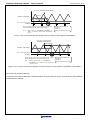
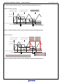
Date: August 22, 2014 RENESAS TECHNICAL UPDATE 1753, Shimonumabe, Nakahara-ku, Kawasaki-shi, Kanagawa 211-8668 Japan Renesas Electronics Corporation Product Category Title MPU/MCU Document No. TN-SH7-A884A/E Usage Notes on A/D Conversion Delaying Function of MTU2 and MTU2S Information Category Technical Notification Reference Document See below. Rev. 1.00 Lot No. Applicable Product See below. All lots Usage notes on A/D conversion delaying function of the multi-function timer pulse unit 2 (MTU2 and MTU2S) for the products listed below are as follows. [Usage Notes] 1. A/D Converter Start Request Enabled Interval If the UT4AE or UT4BE bit is set to 1 in complementary PWM mode, A/D converter start requests are enabled during the TCNT_4 up-counting interval. The A/D converter start request enabled interval is: 0 ≤ TCNT_4 ≤ TCDR − 1. If the DT4AE or DT4BE bit is set to 1 in complementary PWM mode, A/D converter start requests are enabled during the TCNT_4 down-counting interval. The A/D converter start request enabled interval is: TCDR ≥ TCNT_4 ≥ 1. Clear the DT4AE and DT4BE bits to 0 when not in complementary PWM mode. Setting the UT4AE or UT4BE bit to 1 causes an A/D converter start request to be generated at a compare match between TCNT_4 and TADCORA_4/TADCORB_4, regardless of whether TCNT_4 is counting up or down. 2. Notes on Using the A/D Converter Start Request Delaying Function in Complementary PWM Mode When TADCOBRA_4/TADCOBRB_4 is set to 0 and the UT4AE or UT4BE bit in TADCR is set to 1, and then buffer transfer takes place at the trough of TCNT_4, no A/D converter start request occurs during the up-counting interval immediately after the transfer (figure 2.1). When the value of TADCOBRA_4/TADCOBRB_4 is the same as that of TCDR and the DT4AE or DT4BE bit in TADCR is set to 1, and then buffer transfer takes place at the crest of TCNT_4, no A/D converter start request occurs during the down-counting interval immediately after the transfer (figure 2.2). When A/D converter start requests are linked to the interrupt skipping function, set TADCORA_4/TADCORB_4 such that the condition of 2 ≤ TADCORA_4/TADCORB_4 ≤ TCDR − 2 is met. (c) 2014. Renesas Electronics Corporation. All rights reserved. Page 1 of 12 RENESAS TECHNICAL UPDATE TN-SH7-A884A/E Date: August 22, 2014 0 written to TADCOBRA_4/TADCOBRB_4* TCNT_4 TADCORA_4/TADCORB_4 TADCOBRA/B_4 A/D converter start request (TRG4AN) No A/D converter start request occurs during the up-counting interval immediately after the buffer transfer (trough).* Note: * When a value of 1 ≤ TADCOBRA_4/TADCOBRB_4 ≤ TCDR – 1 is written, an A/D converter start request is issued. Complementary PWM mode UT4AE = 1 DT4AE = 0 BF[1:0] = B'10 (transfer at trough) Figure 2.1 A/D Converter Start Request Operation when 0 Is Written to TADCOBRA_4/TADCOBRB_4 Same Value as TCDR written to TADCOBRA_4/TADCOBRB_4* TADCOBRA/B_4 TADCORA_4/TADCORB_4 A/D converter start request (TRG4AN) No A/D converter start request occurs during the up-counting interval immediately after the buffer transfer (crest).* Note: * When a value of TCDR – 1 ≥ TADCOBRA_4/ TADCOBRB_4 ≥ 1 is written, an A/D converter start request is issued. Complementary PWM mode UT4AE = 0 DT4AE = 1 BF[1:0] = B'10 (transfer at crest) Figure 2.2 A/D Converter Start Request Operation when Same Value as TCDR Is Written to TADCOBRA_4/TADCOBRB_4 [Corrections in the User’s Manual] Corrections of the User’s Manual are described below using the SH7214 Group, SH7216 Group User's Manual: Hardware as an example. Page 2 of 12 RENESAS TECHNICAL UPDATE TN-SH7-A884A/E Date: August 22, 2014 11.3.10 Timer A/D Converter Start Request Control Register (TADCR) [Before correction (p.506 to 508)] Bit: 15 14 BF[1:0] Initial value: 0* 0 R/W: R/W R/W 13 0 R 12 0 R 11 0 R 10 0 R 9 0 R 8 0 R 7 6 5 4 3 2 1 0 UT4AE DT4AE UT4BE DT4BE ITA3AE ITA4VE ITB3AE ITB4VE 0* 0* 0* 0* 0* 0* 0 0 R/W R/W R/W R/W R/W R/W R/W R/W Notes: * Do not set to 1 when complementary PWM mode is not selected. Bit Bit Name Initial Value R/W Description 15, 14 BF[1:0] 00 R/W TADCOBRA_4/TADCOBRB_4 Transfer Timing Select Select the timing for transferring data from TADCOBRA_4 and TADCOBRB_4 to TADCORA_4 and TADCORB_4. For details, see table 11.29. 7 UT4AE 0 R/W 6 DT4AE 0* R/W 5 UT4BE 0 R/W 4 DT4BE 0* R/W 3 ITA3AE 0* R/W 2 ITA4VE 0* R/W 1 ITB3AE 0* R/W 0 ITB4VE 0* R/W Up-Count TRG4AN Enable Enables or disables A/D converter start requests (TRG4AN) during TCNT_4 up-count operation. 0: A/D converter start requests (TRG4AN) disabled during TCNT_4 up-count operation 1: A/D converter start requests (TRG4AN) enabled during TCNT_4 up-count operation Down-Count TRG4AN Enable Enables or disables A/D converter start requests (TRG4AN) during TCNT_4 down-count operation. 0: A/D converter start requests (TRG4AN) disabled during TCNT_4 down-count operation 1: A/D converter start requests (TRG4AN) enabled during TCNT_4 down-count operation Up-Count TRG4BN Enable Enables or disables A/D converter start requests (TRG4BN) during TCNT_4 up-count operation. 0: A/D converter start requests (TRG4BN) disabled during TCNT_4 up-count operation 1: A/D converter start requests (TRG4BN) enabled during TCNT_4 up-count operation Down-Count TRG4BN Enable Enables or disables A/D converter start requests (TRG4BN) during TCNT_4 down-count operation. 0: A/D converter start requests (TRG4BN) disabled during TCNT_4 down-count operation 1: A/D converter start requests (TRG4BN) enabled during TCNT_4 down-count operation TGIA_3 Interrupt Skipping Link Enable Select whether to link A/D converter start requests (TRG4AN) with TGIA_3 interrupt skipping operation. 0: Does not link with TGIA_3 interrupt skipping 1: Links with TGIA_3 interrupt skipping TCIV_4 Interrupt Skipping Link Enable Select whether to link A/D converter start requests (TRG4AN) with TCIV_4 interrupt skipping operation. 0: Does not link with TCIV_4 interrupt skipping 1: Links with TCIV_4 interrupt skipping TGIA_3 Interrupt Skipping Link Enable Select whether to link A/D converter start requests (TRG4BN) with TGIA_3 interrupt skipping operation. 0: Does not link with TGIA_3 interrupt skipping 1: Links with TGIA_3 interrupt skipping TCIV_4 Interrupt Skipping Link Enable Select whether to link A/D converter start requests (TRG4BN) with TCIV_4 interrupt skipping operation. 0: Does not link with TCIV_4 interrupt skipping 1: Links with TCIV_4 interrupt skipping Notes: 1. TADCR must not be accessed in eight bits; it should always be accessed in 16 bits. 2. When interrupt skipping is disabled (the T3AEN and T4VEN bits in the timer interrupt skipping set register (TITCR) are cleared to 0 or the skipping count set bits (3ACOR and 4VCOR) in TITCR are cleared to 0), do not link A/D converter start requests with interrupt skipping operation (clear the ITA3AE, ITA4VE, Page 3 of 12 RENESAS TECHNICAL UPDATE TN-SH7-A884A/E Date: August 22, 2014 ITB3AE, and ITB4VE bits in the timer A/D converter start request control register (TADCR) to 0). 3. If link with interrupt skipping is enabled while interrupt skipping is disabled, A/D converter start requests will not be issued. * Do not set to 1 when complementary PWM mode is not selected. [After Correction] Bit: 15 14 BF[1:0] 0 Initial value: 0* R/W: R/W R/W 13 0 R 12 0 R 11 0 R 10 0 R 9 0 R 8 0 R 7 6 5 4 3 2 1 0 UT4AE DT4AE UT4BE DT4BE ITA3AE ITA4VE ITB3AE ITB4VE 0* 0* 0* 0* 0* 0* 0 0 R/W R/W R/W R/W R/W R/W R/W R/W Notes: Accessing TADCR in 8-bit units is prohibited. Always access TADCR in 16-bit units. * Set to 0 when complementary PWM mode is not selected. Bit Bit Name Initial Value 15, 14 BF[1:0] 0* 0 1 R/W Description R/W TADCOBRA_4/TADCOBRB_4 Transfer Timing Select Select the timing for transferring data from TADCOBRA_4 and TADCOBRB_4 to TADCORA_4 and TADCORB_4. For details, see table 11.29. 7 UT4AE 0 R/W Up-Count TRG4AN Enable Enables or disables A/D converter start requests (TRG4AN) during TCNT_4 up-count operation. 0: A/D converter start requests (TRG4AN) are disabled during TCNT_4 up-count operation 1: A/D converter start requests (TRG4AN) are enabled during TCNT_4 up-count operation 6 DT4AE 0* 1 R/W Down-Count TRG4AN Enable Enables or disables A/D converter start requests (TRG4AN) during TCNT_4 down-count operation. 0: A/D converter start requests (TRG4AN) are disabled during TCNT_4 down-count operation 1: A/D converter start requests (TRG4AN) are enabled during TCNT_4 down-count operation 5 UT4BE 0 R/W Up-Count TRG4BN Enable Enables or disables A/D converter start requests (TRG4BN) during TCNT_4 up-count operation. 0: A/D converter start requests (TRG4BN) are disabled during TCNT_4 up-count operation 1: A/D converter start requests (TRG4BN) are enabled during TCNT_4 up-count operation 4 DT4BE 0* 1 R/W Down-Count TRG4BN Enable Enables or disables A/D converter start requests (TRG4BN) during TCNT_4 down-count operation. 0: A/D converter start requests (TRG4BN) are disabled during TCNT_4 down-count operation 1: A/D converter start requests (TRG4BN) are enabled during TCNT_4 down-count operation 3 ITA3AE 1 2 3 0* * * R/W TGIA_3 Interrupt Skipping Link Enable Selects whether to link A/D converter start requests (TRG4AN) with TGIA_3 interrupt skipping operation. 0: Does not link with TGIA_3 interrupt skipping operation 1: Links with TGIA_3 interrupt skipping operation Page 4 of 12 RENESAS TECHNICAL UPDATE TN-SH7-A884A/E Bit Bit 2 Initial Value Name ITA4VE 1 2 3 0* * * R/W Description R/W TCIV_4 Interrupt Skipping Link Enable Date: August 22, 2014 Selects whether to link A/D converter start requests (TRG4AN) with TCIV_4 interrupt skipping operation. 0: Does not link with TCIV_4 interrupt skipping operation 1: Links with TCIV_4 interrupt skipping operation 1 ITB3AE 1 2 3 0* * * R/W TGIA_3 Interrupt Skipping Link Enable Selects whether to link A/D converter start requests (TRG4BN) with TGIA_3 interrupt skipping operation. 0: Does not link with TGIA_3 interrupt skipping operation 1: Links with TGIA_3 interrupt skipping operation 0 ITB4VE 1 2 3 0* * * R/W TCIV_4 Interrupt Skipping Link Enable Selects whether to link A/D converter start requests (TRG4BN) with TCIV_4 interrupt skipping operation. 0: Does not link with TCIV_4 interrupt skipping operation 1: Links with TCIV_4 interrupt skipping operation Notes: 1. Set to 0 when complementary PWM mode is not selected. 2. Clear this bit to 0 when interrupt skipping is disabled (when the T3AEN or T4VEN bit in the timer interrupt skipping set register (TITCR) is cleared to 0 or when the skipping count set bit (3ACOR or 4VCOR) in TITCR is cleared to 0). 3. If link with interrupt skipping is enabled while interrupt skipping is disabled, A/D converter start requests will not be issued. [Before correction (p.508)] Table 11.29 Setting of Transfer Timing by Bits BF1 and BF0 Bit 7 Bit 6 BF1 BF0 Description Does not transfer data from the cycle set buffer register to the cycle set register. Transfers data from the cycle set buffer register to the cycle set register at the 0 1 1 crest of the TCNT_4 count.* Transfers data from the cycle set buffer register to the cycle set register at the 1 0 2 trough of the TCNT_4 count.* Transfers data from the cycle set buffer register to the cycle set register at the 1 1 2 crest and trough of the TCNT_4 count.* Notes: 1. Data is transferred from the cycle set buffer register to the cycle set register when the crest of the TCNT_4 0 0 count is reached in complementary PWM mode, when compare match occurs between TCNT_3 and TGRA_3 in reset-synchronized PWM mode, or when compare match occurs between TCNT_4 and TGRA_4 in PWM mode 1 or normal operation mode. 2. These settings are prohibited when complementary PWM mode is not selected. Page 5 of 12 RENESAS TECHNICAL UPDATE TN-SH7-A884A/E Date: August 22, 2014 [After correction] Table 11.29 Setting of Transfer Timing by BF[1:0] Bits Bit 15 Bit 14 Description BF1 BF0 Complementary PWM Mode Reset-Synchronized PWM Mode 0 0 0 1 Does not transfer data from the cycle set buffer register (TADCOBRA_4/TADCOBRB_4) to the cycle set register (TADCORA_4/TADCORB_4). Transfers data from the cycle set buffer register (TADCOBRA_4/TADCOBRB_4) to the cycle set register (TADCORA_4/TADCORB_4) at the crest of TCNT_4. 1 0 Does not transfer data from the cycle set buffer register (TADCOBRA_4/TADCOBRB_4) to the cycle set register (TADCORA_4/TADCORB_4). Transfers data from the cycle set buffer register (TADCOBRA_4/TADCOBRB_4) to the cycle set register (TADCORA_4/TADCORB_4) when a compare match occurs between TCNT_3 and TGRA_3. Setting prohibited 1 1 Bit 15 Bit 14 BF1 BF0 PWM Mode 1 Normal Mode 0 0 0 1 Does not transfer data from the cycle set buffer register (TADCOBRA_4/TADCOBRB_4) to the cycle set register (TADCORA_4/TADCORB_4). Transfers data from the cycle set buffer register (TADCOBRA_4/TADCOBRB_4) to the cycle set register (TADCORA_4/TADCORB_4) when a compare match occurs between TCNT_4 and TGRA_4. 1 0 Setting prohibited Does not transfer data from the cycle set buffer register (TADCOBRA_4/TADCOBRB_4) to the cycle set register (TADCORA_4/TADCORB_4). Transfers data from the cycle set buffer register (TADCOBRA_4/TADCOBRB_4) to the cycle set register (TADCORA_4/TADCORB_4) when a compare match occurs between TCNT_4 and TGRA_4. Setting prohibited 1 1 Setting prohibited Setting prohibited Transfers data from the cycle set buffer register (TADCOBRA_4/TADCOBRB_4) to the cycle set register (TADCORA_4/TADCORB_4) at the trough of TCNT_4. Transfers data from the cycle set buffer register (TADCOBRA_4/TADCOBRB_4) to the cycle set register (TADCORA_4/TADCORB_4) at the crest and trough of TCNT_4. Setting prohibited Description Page 6 of 12 RENESAS TECHNICAL UPDATE TN-SH7-A884A/E 11.4.9 Date: August 22, 2014 A/D Converter Start Request Delaying Function Example of Procedure for Specifying A/D Converter Start Request Delaying Function [Before correction (p.615)] [1] Set the cycle in the timer A/D converter start request cycle buffer register (TADCOBRA_4 or TADCOBRB_4) and timer A/D converter start request cycle register (TADCORA_4 or TADCORB_4). (The same initial value must be specified in the cycle buffer register and cycle register.) A/D converter start request delaying function Set A/D converter start request cycle • Set the timing of transfer from cycle set buffer register • Set linkage with interrupt skipping • Enable A/D converter start request delaying function [1] [2] Use bits BF1 and BF2 in the timer A/D converter start request control register (TADCR) to specify the timing of transfer from the timer A/D converter start request cycle buffer register to A/D converter start request cycle register. • Specify whether to link with interrupt skipping through bits ITA3AE, ITA4VE, ITB3AE, and ITB4VE. • Use bits TU4AE, DT4AE, UT4BE, and DT4BE to enable A/D conversion start requests (TRG4AN or TRG4BN). [2] Notes: 1. Perform TADCR setting while TCNT_4 is stopped. 2. Do not set BF1 to 1 when complementary PWM mode is not selected. 3. Do not set ITA3AE, ITA4VE, ITB3AE, ITB4VE, DT4AE, or DT4BE to 1when complementary PWM mode is not selected. A/D converter start request delaying function Figure 11.79 Example of Procedure for Specifying A/D Converter Start Request Delaying Function [After correction] [1] Set the cycle in the timer A/D converter start request cycle buffer register (TADCOBRA_4 or TADCOBRB_4) and timer A/D converter start request cycle register (TADCORA_4 or TADCORB_4). (The same initial value must be specified in the cycle buffer register and cycle register.) A/D converter start request delaying function Set A/D converter start request cycle • Set the timing of transfer from cycle set buffer register • Set linkage with interrupt skipping • Enable A/D converter start request delaying function A/D converter start request delaying function [1] [2] [2] Use bits BF[1:0] in the timer A/D converter start request control register (TADCR) to specify the timing of transfer from the timer A/D converter start request cycle buffer register to A/D converter start request cycle register. • Specify whether to link with interrupt skipping through bits ITA3AE, ITA4VE, ITB3AE, and ITB4VE. • Use bits TU4AE, DT4AE, UT4BE, and DT4BE to enable A/D conversion start requests (TRG4AN or TRG4BN). Notes: 1. Perform TADCR setting while TCNT_4 is stopped. 2. Set BF1 bit to 0 when complementary PWM mode is not selected. 3. Set ITA3AE, ITA4VE, ITB3AE, ITB4VE, DT4AE, or DT4BE bits to 0 when complementary PWM mode is not selected. 4. Clear the ITA3AE, ITA4VE, ITB3AE, or ITB4VE bit to 0 to disable interrupt skipping. Figure 11.79 Example of Procedure for Specifying A/D Converter Start Request Delaying Function Page 7 of 12 RENESAS TECHNICAL UPDATE TN-SH7-A884A/E Date: August 22, 2014 Basic Operation Example of A/D Converter Start Request Delaying Function [Before correction (p.616)] Transfer from cycle buffer register to cycle register Transfer from cycle buffer register to cycle register Transfer from cycle buffer register to cycle register TADCORA_4 TCNT_4 TADCOBRA_4 A/D converter start request (TRG4AN) (Complementary PWM mode) Figure 11.80 Basic Example of A/D Converter Start Request Signal (TRG4AN) Operation [After Correction] Transfer from cycle buffer register to cycle register Transfer from cycle buffer register to cycle register A/D converter start request enabled interval (DT4AE) A/D converter start request enabled interval (UT4AE) TADCORA_4 TCNT_4 TADCOBRA_4 A/D converter start request (TRG4AN) 0 ≤ TCNT_4 ≤ TCDR – 1 A/D converter start request enabled interval (DT4AE): TCDR ≥ TCNT_4 ≥ 1 A/D converter start request enabled interval (UT4AE): Complementary PWM mode UT4AE = 0 DT4AE = 1 BF[1:0] = B'10 Figure 11.80 Basic Example of A/D Converter Start Request Signal (TRG4AN) Operation Page 8 of 12 RENESAS TECHNICAL UPDATE TN-SH7-A884A/E Date: August 22, 2014 [Addition (p.616): to be added after the section of “Basic Operation Example of A/D Converter Start Request Delaying Function”] A/D Converter Start Request Enabled Interval When TCNT_4 and TADCORA_4/TADCORB_4 match during the interval enabled by theUT4AE, DT4AE, UT4BE, or DT4BE bit in TADCR, a start request is issued for the corresponding A/D converter (TRG4AN or TRG4BN). If the UT4AE or UT4BE bit is set to 1 in complementary PWM mode, A/D converter start requests are enabled during the TCNT_4 up-counting interval (0 ≤ TCNT_4 ≤ TCDR − 1). A/D converter start requests are enabled during the TCNT_4 down-counting interval (TCDR ≥ TCNT_4 ≥ 1) if the DT4AE or DT4BE bit is set to 1 (figure 11.80). Clear the DT4AE and DT4BE bits to 0 when not in complementary PWM mode. Setting the UT4AE or UT4BE bit to 1 causes an A/D converter start request to be generated at a compare match between TCNT_4 and TADCORA_4/TADCORB_4, regardless of whether TCNT_4 is counting up or down. Buffer Transfer [Before correction (p.616)] The data in the timer A/D converter start request cycle set registers (TADCORA_4 and TADCORB_4) is updated by writing data to the timer A/D converter start request cycle set buffer registers (TADCOBRA_4 and TADCOBRB_4). Data is transferred from the buffer registers to the respective cycle set registers at the timing selected with the BF1 and BF0 bits in the timer A/D converter start request control register (TADCR_4). [After Correction] The data in the timer A/D converter start request cycle set registers (TADCORA_4 and TADCORB_4) is updated by writing data to the timer A/D converter start request cycle set buffer registers (TADCOBRA_4 and TADCOBRB_4). Data is transferred from the buffer registers to the respective cycle set registers at the timing selected with the BF[1:0] bits in the timer A/D converter start request control register (TADCR). When using buffer transfer in complementary PWM mode, exercise care regarding the buffer transfer timing. For details, see 11.7.24, Notes on Using the A/D Converter Start Request Delaying Function in Complementary PWM Mode. Also, clear the BF1 bit to 0 when not in complementary PWM mode. Page 9 of 12 RENESAS TECHNICAL UPDATE TN-SH7-A884A/E Date: August 22, 2014 A/D Converter Start Request Delaying Function Linked with Interrupt Skipping [Before correction (p.616 to 617)] A/D converter start requests (TRG4AN and TRG4BN) can be issued in coordination with interrupt skipping by making settings in the ITA3AE, ITA4VE, ITB3AE, and ITB4VE bits in the timer A/D converter start request control register (TADCR). Figure 11.81 shows an example of A/D converter start request signal (TRG4AN) operation when TRG4AN output is enabled during TCNT_4 up-counting and down-counting and A/D converter start requests are linked with interrupt skipping. Figure 11.82 shows another example of A/D converter start request signal (TRG4AN) operation when TRG4AN output is enabled during TCNT_4 up-counting and A/D converter start requests are linked with interrupt skipping. Note: This function must be used in combination with interrupt skipping. When interrupt skipping is disabled (the T3AEN and T4VEN bits in the timer interrupt skipping set register (TITCR) are cleared to 0 or the skipping count set bits (3ACOR and 4VCOR) in TITCR are cleared to 0), make sure that A/D converter start requests are not linked with interrupt skipping (clear the ITA3AE, ITA4VE, ITB3AE, and ITB4VE bits in the timer A/D converter start request control register (TADCR) to 0). [After Correction] In complementary PWM mode, A/D converter start requests (TRG4AN and TRG4BN) can be issued in coordination with interrupt skipping by making settings in the ITA3AE, ITA4VE, ITB3AE, and ITB4VE bits in the timer A/D converter start request control register (TADCR). Figure 11.81 shows an example of A/D converter start request signal (TRG4AN) operation when TRG4AN output is enabled during TCNT_4 up-counting and down-counting and A/D converter start requests are linked with interrupt skipping. Figure 11.82 shows another example of A/D converter start request signal (TRG4AN) operation when TRG4AN output is enabled during TCNT_4 up-counting and A/D converter start requests are linked with interrupt skipping. The A/D converter start request delaying function linked to the interrupt skipping function cannot be used when not in complementary PWM mode. In this case, clear the ITA3AE, ITA4VE, ITB3AE, and ITB4VE bits in TADCR to 0. Note: This function must be used in combination with interrupt skipping. When interrupt skipping is disabled (the T3AEN and T4VEN bits in the timer interrupt skipping set register (TITCR) are cleared to 0 or the skipping count set bits (3ACOR and 4VCOR) in TITCR are cleared to 0), make sure that A/D converter start requests are not linked with interrupt skipping (clear the ITA3AE, ITA4VE, ITB3AE, and ITB4VE bits in the timer A/D converter start request control register (TADCR) to 0). Furthermore, when this function is to be used, set TADCORA_4 and TADCORB_4 to a value between H'0002 and the TCDR setting minus two. Page 10 of 12 RENESAS TECHNICAL UPDATE TN-SH7-A884A/E Date: August 22, 2014 [Addition (p.629)] 11.7.24 Notes on Using the A/D Converter Start Request Delaying Function in Complementary PWM Mode When TADCOBRA_4/TADCOBRB_4 is set to 0 and the UT4AE or UT4BE bit in TADCR is set to 1, and then buffer transfer takes place at the trough of TCNT_4, no A/D converter start request occurs during the up-counting interval immediately after the transfer (figure 11.139). When the value of TADCOBRA_4/TADCOBRB_4 is the same as that of TCDR and the DT4AE or DT4BE bit in TADCR is set to 1, and then buffer transfer takes place at the crest of TCNT_4, no A/D converter start request occurs during the down-counting interval immediately after the transfer (figure 11.140). When A/D converter start requests are linked to the interrupt skipping function, set TADCORA_4/TADCORB_4 such that the condition of 2 ≤ TADCORA_4/TADCORB_4 ≤ TCDR - 2 is met. 0 written to TADCOBRA_4/TADCOBRB_4* TCNT_4 TADCORA_4/TADCORB_4 TADCOBRA/B_4 A/D converter start request (TRG4AN) No A/D converter start request occurs during the up-counting interval immediately after the buffer transfer (trough).* Note: * When a value of 1 ≤ TADCOBRA_4/TADCOBRB_4 ≤ TCDR – 1 is written, an A/D converter start request is issued. Complementary PWM mode UT4AE = 1 DT4AE = 0 BF[1:0] = B'10 (transfer at trough) Figure 11.139 A/D Converter Start Request Operation when 0 Is Written to TADCOBRA_4/TADCOBRB_4 Same Value as TCDR written to TADCOBRA_4/TADCOBRB_4* TADCOBRA/B_4 TADCORA_4/TADCORB_4 A/D converter start request (TRG4AN) No A/D converter start request occurs during the up-counting interval immediately after the buffer transfer (crest).* Note: * When a value of TCDR – 1 ≥ TADCOBRA_4/ TADCOBRB_4 ≥ 1 is written, an A/D converter start request is issued. Complementary PWM mode UT4AE = 0 DT4AE = 1 BF[1:0] = B'10 (transfer at crest) Figure 11.140 A/D Converter Start Request Operation when Same Value as TCDR Is Written to TADCOBRA_4/TADCOBRB_4 Page 11 of 12 RENESAS TECHNICAL UPDATE TN-SH7-A884A/E Date: August 22, 2014 [Applicable Products and Reference Documents] Series Group SH7080 SH7083, SH7084, SH7085, SH7086 SH7137 SH7131, SH7132, Reference Document Rev. Ref. No. SH7080 Group User's Manual: Hardware 5.00 R01UH0198EJ0500 SH7137 Group Hardware Manual 3.00 REJ09B0402-0300 SH7136, SH7137 SH7146 SH7146, SH7149 SH7146 Group User's Manual: Hardware 4.00 R01UH0049EJ0400 SH7200 SH7201 SH7201 Group User's Manual: Hardware 3.00 R01UH0026EJ0300 SH7203 SH7203 Group User's Manual: Hardware 4.00 R01UH0458EJ0400 SH7205 SH7205 Group Hardware Manual 2.00 REJ09B0372-0200 SH7206 SH7206 Group User's Manual: Hardware 4.00 R01UH0283EJ0400 SH7210 SH7211 SH7211 Group Hardware Manual 3.00 REJ09B0344-0300 SH7216 SH7214, SH7216 SH7214 Group, SH7216 Group User's Manual: 4.00 R01UH0230EJ0400 Hardware SH7231 SH7231 SH7231 Group User's Manual: Hardware 2.00 R01UH0073EJ0200 SH7239 SH7237, SH7239 SH7239 Group, SH7237 Group User's Manual: 2.00 R01UH0086EJ0200 3.00 R01UH0229EJ0300 R01UH0025EJ0300 Hardware SH7243 SH7243 SH7280 Group, SH7243 Group User's Manual: Hardware SH7260 SH7261 SH7261 Group User's Manual: Hardware 3.00 SH7262, SH7264 SH7262 Group, SH7264 Group User's Manual: 3.00 Hardware R01UH0134EJ0300 SH7263 SH7263 Group User's Manual: Hardware 4.00 R01UH0459EJ0400 SH7265 SH7265 Group Hardware Manual 2.00 REJ09B0351-0200 SH7266, SH7267 SH7266 Group, SH7267 Group User's Manual: 2.00 Hardware SH7268, SH7269 SH7268 Group, SH7269 Group User's Manual: R01UH0412EJ0200 2.00 Hardware SH726A, SH726B SH726A Group, SH726B Group User's Manual: R01UH0048EJ0200 1.00 Hardware SH7280 SH7285, SH7286 SH7280 Group, SH7243 Group User's Manual: R01UH0202EJ0100 3.00 R01UH0229EJ0300 5.00 REJ09B0243-0500 Hardware SH/Tiny SH7124, SH7125 SH7125 Group, SH7124 Group Hardware Manual End of Document Page 12 of 12