1
UM1762
User manual
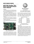
SPC560P-DISP Discovery+ evaluation board
Introduction
The SPC560P-DISP Discovery kit helps you to discover SPC56 P line Power Architecture®
Microcontrollers.
The discovery board is based on SPC560P50L5, 64 MHz, single issue, 32-bit CPU core
complex (e200z0h) CPU core with 574KB flash in an LQFP144 package.
The numerous interfaces including GPI/O's, peripherals such as CAN, JTAG, K-Line, LIN,
FlexCAN and GPIOs make the SPC560P-DISP an excellent starter kit for customer quick
evaluation and project development.
Dedicated connectors allow plugging Arduino shields (Arduino-compatible).
The SPC560 P line is designed to address cost sensitive chassis, airbag, electrical
hydraulic power steering (EHPS), electric power steering (EPS), and electrical motor control
applications.
Free ready-to-run application firmware examples are available inside SPC5Studio
(www.st.com/spc5studio) to support quick evaluation and development.
May 2014
DocID026329 Rev 1
1/24
www.st.com
Contents
UM1762
Contents
1
2
SPC560P-DISP Discovery+ board . . . . . . . . . . . . . . . . . . . . . . . . . . . . . . 5
1.1
Debug interface . . . . . . . . . . . . . . . . . . . . . . . . . . . . . . . . . . . . . . . . . . . . . 5
1.2
I/O interface and connectors . . . . . . . . . . . . . . . . . . . . . . . . . . . . . . . . . . . 5
Hardware overview . . . . . . . . . . . . . . . . . . . . . . . . . . . . . . . . . . . . . . . . . . 6
2.1
3
Power Supply section . . . . . . . . . . . . . . . . . . . . . . . . . . . . . . . . . . . . . . . . . 6
2.1.1
5 VDC power supply . . . . . . . . . . . . . . . . . . . . . . . . . . . . . . . . . . . . . . . . 7
2.1.2
3.3 VDC power supply . . . . . . . . . . . . . . . . . . . . . . . . . . . . . . . . . . . . . . 8
2.1.3
Power supply using USB connection . . . . . . . . . . . . . . . . . . . . . . . . . . . . 8
2.1.4
Automatic DC source selector . . . . . . . . . . . . . . . . . . . . . . . . . . . . . . . . . 9
2.2
Crystal oscillator . . . . . . . . . . . . . . . . . . . . . . . . . . . . . . . . . . . . . . . . . . . . . 9
2.3
Reset section . . . . . . . . . . . . . . . . . . . . . . . . . . . . . . . . . . . . . . . . . . . . . . 10
2.4
User LEDs . . . . . . . . . . . . . . . . . . . . . . . . . . . . . . . . . . . . . . . . . . . . . . . . 10
2.5
ADC reference . . . . . . . . . . . . . . . . . . . . . . . . . . . . . . . . . . . . . . . . . . . . . 10
2.6
Integrated USB programmer/debugger . . . . . . . . . . . . . . . . . . . . . . . . . . .11
2.7
JTAG connectors . . . . . . . . . . . . . . . . . . . . . . . . . . . . . . . . . . . . . . . . . . . 13
2.8
FlexCAN interface and Safety Port . . . . . . . . . . . . . . . . . . . . . . . . . . . . . 15
2.9
FlexRay interface . . . . . . . . . . . . . . . . . . . . . . . . . . . . . . . . . . . . . . . . . . . 15
2.10
LINFlex communication (Serial Communication Interface module) . . . . . 16
2.11
Connectors Arduino-compatible . . . . . . . . . . . . . . . . . . . . . . . . . . . . . . . . 17
2.12
I/O header . . . . . . . . . . . . . . . . . . . . . . . . . . . . . . . . . . . . . . . . . . . . . . . . 18
PCB layout . . . . . . . . . . . . . . . . . . . . . . . . . . . . . . . . . . . . . . . . . . . . . . . . 21
Appendix A General handling precautions . . . . . . . . . . . . . . . . . . . . . . . . . . . . . 22
Revision history . . . . . . . . . . . . . . . . . . . . . . . . . . . . . . . . . . . . . . . . . . . . . . . . . . . . 23
2/24
DocID026329 Rev 1
UM1762
List of tables
List of tables
Table 1.
Table 2.
Table 3.
Table 4.
Table 5.
PSU Section - LEDs . . . . . . . . . . . . . . . . . . . . . . . . . . . . . . . . . . . . . . . . . . . . . . . . . . . . . . . 7
User LEDs . . . . . . . . . . . . . . . . . . . . . . . . . . . . . . . . . . . . . . . . . . . . . . . . . . . . . . . . . . . . . 10
JTAG connector (X1 and X2) . . . . . . . . . . . . . . . . . . . . . . . . . . . . . . . . . . . . . . . . . . . . . . . 14
I/O header (Schematic diagram). . . . . . . . . . . . . . . . . . . . . . . . . . . . . . . . . . . . . . . . . . . . . 19
Document revision history . . . . . . . . . . . . . . . . . . . . . . . . . . . . . . . . . . . . . . . . . . . . . . . . . 23
DocID026329 Rev 1
3/24
3
List of figures
UM1762
List of figures
Figure 1.
Figure 2.
Figure 3.
Figure 4.
Figure 5.
Figure 6.
Figure 7.
Figure 8.
Figure 9.
Figure 10.
Figure 11.
Figure 12.
Figure 13.
Figure 14.
Figure 15.
Figure 16.
Figure 17.
Figure 18.
Figure 19.
Figure 20.
Figure 21.
Figure 22.
Figure 23.
Figure 24.
Figure 25.
Figure 26.
Figure 27.
Figure 28.
Figure 29.
4/24
SPC560P-DISP Discovery+ board . . . . . . . . . . . . . . . . . . . . . . . . . . . . . . . . . . . . . . . . . . . . 5
SPC560P-DISP - hw overview . . . . . . . . . . . . . . . . . . . . . . . . . . . . . . . . . . . . . . . . . . . . . . . 6
PSU section (PCB top side) . . . . . . . . . . . . . . . . . . . . . . . . . . . . . . . . . . . . . . . . . . . . . . . . . 6
PSU section (PCB bottom side) . . . . . . . . . . . . . . . . . . . . . . . . . . . . . . . . . . . . . . . . . . . . . . 7
PSU section (Vout: 5.0 VDC). . . . . . . . . . . . . . . . . . . . . . . . . . . . . . . . . . . . . . . . . . . . . . . . . 8
PSU section (Vout: 3.3 VDC). . . . . . . . . . . . . . . . . . . . . . . . . . . . . . . . . . . . . . . . . . . . . . . . . 8
USB connection - 3.3 VDC. . . . . . . . . . . . . . . . . . . . . . . . . . . . . . . . . . . . . . . . . . . . . . . . . . . . . . . . . . . . . . . . 8
Automatic DC source selector . . . . . . . . . . . . . . . . . . . . . . . . . . . . . . . . . . . . . . . . . . . . . . . 9
Crystal oscillator . . . . . . . . . . . . . . . . . . . . . . . . . . . . . . . . . . . . . . . . . . . . . . . . . . . . . . . . . . 9
Reset section . . . . . . . . . . . . . . . . . . . . . . . . . . . . . . . . . . . . . . . . . . . . . . . . . . . . . . . . . . . 10
User LEDs . . . . . . . . . . . . . . . . . . . . . . . . . . . . . . . . . . . . . . . . . . . . . . . . . . . . . . . . . . . . . 10
ADC reference . . . . . . . . . . . . . . . . . . . . . . . . . . . . . . . . . . . . . . . . . . . . . . . . . . . . . . . . . . 11
Integrated debugger – USB input . . . . . . . . . . . . . . . . . . . . . . . . . . . . . . . . . . . . . . . . . . . . 12
Integrated debugger – EEPROM . . . . . . . . . . . . . . . . . . . . . . . . . . . . . . . . . . . . . . . . . . . . 12
Integrated debugger - Level Shifters . . . . . . . . . . . . . . . . . . . . . . . . . . . . . . . . . . . . . . . . . 13
Integrated debugger - LEDs . . . . . . . . . . . . . . . . . . . . . . . . . . . . . . . . . . . . . . . . . . . . . . . . 13
JTAG connectors . . . . . . . . . . . . . . . . . . . . . . . . . . . . . . . . . . . . . . . . . . . . . . . . . . . . . . . . 14
FlexCAN - jumpers configuration . . . . . . . . . . . . . . . . . . . . . . . . . . . . . . . . . . . . . . . . . . . . 15
High Speed CAN and FlexRay . . . . . . . . . . . . . . . . . . . . . . . . . . . . . . . . . . . . . . . . . . . . . . 15
FlexRay – jumper configuration . . . . . . . . . . . . . . . . . . . . . . . . . . . . . . . . . . . . . . . . . . . . . 16
FlexRay transceiver and connector . . . . . . . . . . . . . . . . . . . . . . . . . . . . . . . . . . . . . . . . . . 16
LINFlex communication (I) . . . . . . . . . . . . . . . . . . . . . . . . . . . . . . . . . . . . . . . . . . . . . . . . . 17
LINFlex communication (I) . . . . . . . . . . . . . . . . . . . . . . . . . . . . . . . . . . . . . . . . . . . . . . . . . 17
Connectors Arduino-compatible (I) . . . . . . . . . . . . . . . . . . . . . . . . . . . . . . . . . . . . . . . . . . . 17
Connectors Arduino-compatible (II) . . . . . . . . . . . . . . . . . . . . . . . . . . . . . . . . . . . . . . . . . . 18
Connectors Arduino-compatible (III) . . . . . . . . . . . . . . . . . . . . . . . . . . . . . . . . . . . . . . . . . . 18
Connectors Arduino-compatible (IV). . . . . . . . . . . . . . . . . . . . . . . . . . . . . . . . . . . . . . . . . . 18
I/O header (Schematic diagram). . . . . . . . . . . . . . . . . . . . . . . . . . . . . . . . . . . . . . . . . . . . . 19
PCB layout . . . . . . . . . . . . . . . . . . . . . . . . . . . . . . . . . . . . . . . . . . . . . . . . . . . . . . . . . . . . . 21
DocID026329 Rev 1
UM1762
1
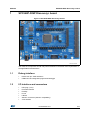
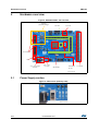
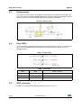
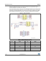
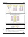
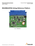
SPC560P-DISP Discovery+ board
SPC560P-DISP Discovery+ board
Figure 1. SPC560P-DISP Discovery+ board
("1(3*
The PCB, the components and all HW parts assembled in the board meet requirements of
the applicable RoHS directives.
1.1
1.2
Debug interface
•
Double 2x7-pin JTAG interfaces
•
USB mini B and integrated programmer/debugger
I/O interface and connectors
•
PSU plug (+12V)
•
FlexCAN interface
•
FlexRay
•
K-Line
•
LINFlex
•
Arduino connectors (Arduino compatibility)
•
4x37 headers
DocID026329 Rev 1
5/24
23
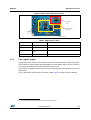
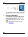
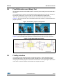
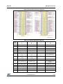
Hardware overview
2
UM1762
Hardware overview
Figure 2. SPC560P-DISP - hw overview
,QWHJUDWHG
SURJUDPPHUGHEXJJHU
8VHU/('V
8VHU/('V
-7$*FRQQHFWRU
5HVHW
9'& SRZHU6XSSO\
DQGVZLWFK
368DQG
9/('V
3RWHQWLRPHWHU
IRU$'&
63&3/
("1(3*
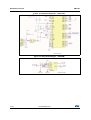
2.1
Power Supply section
Figure 3. PSU section (PCB top side)
("1(3*
6/24
DocID026329 Rev 1
[+HDGHU
UM1762
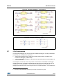
Hardware overview
Figure 4. PSU section (PCB bottom side)
96XSSO\
8
'&VRXUFH6HOHFWRU
88
96XSSO\
8
("1(3*
Table 1. PSU Section - LEDs
Item
2.1.1
Color
Function
D7
Green
Vext (+12V)
D8
Green
5V
D9
Green
D3
Green
3.3V
VCIO
5 VDC power supply
This section is only used when an external 12V PSU is connected to the X5 DC port(a) (X5).
The diode D6 is used to protect the board against reverse polarity and AC source. The fuse
F1 protects the board when an accidental short circuit occurs.
The LED D7 is switched on when the board is correctly powered and the switch S1 is set to
ON position.
The 5V generator is based on the ST device A7985; Figure 5 shows the circuit diagram.
a.
The external 12V PSU adapter is not included in the evaluation kit
DocID026329 Rev 1
7/24
23
Hardware overview
UM1762
Figure 5. PSU section (Vout: 5.0 VDC)
("1(3*
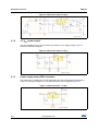
2.1.2
3.3 VDC power supply
The liner regulator LD1117-3V3 is used to generate the 3.3 V supply voltage; Figure 6
shows the schematic diagram.
Figure 6. PSU section (Vout: 3.3 VDC)
("1(3*
2.1.3
Power supply using USB connection
The board can be supplied by the USB cable when the internal programmer/debugger is
used; in this working condition 3.3 V is generated using a liner regulator (Figure 7).
Figure 7. USB connection - 3.3 VDC
("1(3*
8/24
DocID026329 Rev 1
UM1762
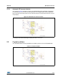
2.1.4
Hardware overview
Automatic DC source selector
The circuit in Figure 8 switches 5 V and 3.3 V automatically when the board is supplied by
an external PSU or by 5V from the PC/USB cable. The voltage divider made by R46 and
R51 is used to sense the presence of an external PSU (5V is sensed) and it drives U19 and
U23 properly.
Figure 8. Automatic DC source selector
("1(3*
The jumper JP24 allows selecting the VDD_HV level: 3.3 V or 5 V.
2.2
Crystal oscillator
The SPC560P-DISP board is populated with 16 MHz crystal to clock the SPC560P50L5.
Figure 9. Crystal oscillator
("1(3*
DocID026329 Rev 1
9/24
23
Hardware overview
2.3
UM1762
Reset section
The reset circuit (see Figure 10) generates a sharp signal to reset the microcontroller. The
core of the circuit is the device STM6315RB-2.63 V; it produces the reset pulse when the S3
button is pushed: D14 is turned on on when the reset pulse is generated.
Figure 10. Reset section
("1(3*
2.4
User LEDs
On the board are present three USER LEDs connected as shown in Figure 11. The jumpers
JP13, JP14 and JP18 allow disconnecting the LED cathodes and used the GPIO to a
different purpose.
Figure 11. User LEDs
("1(3*
Table 2. User LEDs
Item
2.5
Color
µC Pin - function
D11
Green
A0_eTIMER0_ETC0
D12
Green
A1_eTIMER0_ETC1
D13
Green
G4_FlexPWM0_B2
ADC reference
Jumper JP 12 allows setting the ADC reference level: 5 V or 3.3 V.
10/24
DocID026329 Rev 1
UM1762
Hardware overview
Figure 12. ADC reference
("1(3*
Two potentiometers (R56 and R57) and the jumpers JP19 and JP20 allow the user to
quickly evaluate the performance of ADC: the analog voltage can be adjusted in the range is
0 ÷ VDD_HV_ADC.
Removing the jumper the pin E0 and E12 can be used to support a different application.
2.6
Integrated USB programmer/debugger
The integrated debugger, based on the device FTDI2232H and UDE PLS software, allows
the user to build, run and debug the software applications.
The integrated debugger can be configured to operate as standalone unit and used to
program and debug another SPC5xx application or an evaluation boards. The board is
configured to operate using the integrated debugger.
The SPC560P-DISP discovery board includes a full-featured, perpetual code-limited (128
Kbytes) PLS software license. The debugger serial number is reported on a label applied on
the board.
To download the debugger software and to activate license go to the PLS website.
The integrated debugger is accessible via ST's free integrated development environment,
SPC5Studio (www.st.com/spc5studio).
DocID026329 Rev 1
11/24
23
Hardware overview
UM1762
Figure 13. Integrated debugger – USB input
("1(3*
Figure 14. Integrated debugger – EEPROM
("1(3*
12/24
DocID026329 Rev 1
UM1762
Hardware overview
Figure 15. Integrated debugger - Level Shifters
("1(3*
Figure 16. Integrated debugger - LEDs
("1(3*
2.7
JTAG connectors
The integrated debugger can also be used as standalone debugger. To make possible this
functionality, two HW options are possible:
1.
Remove the debugger for the main board cutting small portions of PCB where is
located the debugger; (cutable PCB).
2.
Let the integrated PLS adapter on the board and electrically disconnect the adapter to
the microcontroller
The first option consists to remove the portion of PCB where is assembled the debugger
cutting small portion of PCB. Both the debugger and the discovery board do notneed HW
modification to work properly(b). A JTAG connector (X1) present in the detached
debugger/programmer allows connecting the board to a target application. Level shifters are
b.
Removing the integrated adapter the discovery board must be supplied using a PSU
DocID026329 Rev 1
13/24
23
Hardware overview
UM1762
present to equalize the I/O levels. The discovery board can be programmed using an
external programmer connected to the JTAG X2.
The second solution does not need to remove the debugger because it can be disconnected
electrically removing the array resistor RP1. The two JTAG connectors allow connecting the
programmer to the target application. The discovery board must be supplied using a PSU
and a programmer must be connected to the JTAG port to program the microcontroller.
Figure 17. JTAG connectors
("1(3*
Table 3. JTAG connector (X1 and X2)
14/24
Pin
Signal
Pin
Signal
1
TDI
2
GND
3
TDO
4
GND
5
TCK
6
GND
7
EVTI
8
NC
9
RESET
10
TMS
11
VDDE7
12
GND
13
RDY
14
JCOMP
DocID026329 Rev 1
UM1762
2.8
Hardware overview
FlexCAN interface and Safety Port
SPC560P50L5 includes a FlexCAN interface controller (version 2.0B), the transceiver and a
connector.
The controller also includes a second CAN controller synthesized to run at high bit rates to
be used as a safety port. It can be used as a second independent CAN module.
JP22 and JP23 allow selecting the CAN channel connected to the transceiver; see
Figure 18. JP10 connects the 120 Ω termination resistor (the resistor is connected when the
jumper is present).
Figure 18. FlexCAN - jumpers configuration
("1(3*
The CAN output signals are available in a single 2x8 pin male connector (see U24 in
Figure 19); the FlexCAN output signals are connected to the even pins of the connector.
Figure 19. High Speed CAN and FlexRay
("1(3*
2.9
FlexRay interface
The FlexRay module implements the Protocol Specification 2.1 with selectable single or
dual channel support. The transceiver used is TJA1080 (U15); JP7, JP8 and JP9 allow
configuring the FlaxRay signals connected to the transceiver. The output signals are located
in the same connector used for the FlexCAN, the odd pins are used.
DocID026329 Rev 1
15/24
23
Hardware overview
UM1762
Figure 20. FlexRay – jumper configuration
("1(3*
Figure 21. FlexRay transceiver and connector
("1(3*
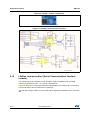
2.10
LINFlex communication (Serial Communication Interface
module)
The LINFlex supports LIN Master mode, LIN Slave mode and UART mode. LIN state
machine is compliant to LIN1.3, 2.0, and 2.1 specifications.
Figure 22 and Figure 23 show the hardware implemented for the UART/LIN: U18 and U14
are the LIN and the K-Line transceivers respectively.
JP4 and JP5 configure UART or LIN; the RX and SX signals are available on the connector
JP6.
16/24
DocID026329 Rev 1
UM1762
Hardware overview
Figure 22. LINFlex communication (I)
("1(3*
Figure 23. LINFlex communication (I)
("1(3*
2.11
Connectors Arduino-compatible
In this discovery board are present Arduino compatible: the connectors J1 J2, J4 and J5 are
compatible with the Arduino-UNO shields and the J5, J6, and JP2 are compatible with
Arduino-Mega shields.
The figures here below are showing the connections of the microcontroller pins and the
Arduino connectors.
Figure 24. Connectors Arduino-compatible (I)
("1(3*
DocID026329 Rev 1
17/24
23
Hardware overview
UM1762
Figure 25. Connectors Arduino-compatible (II)
("1(3*
Figure 26. Connectors Arduino-compatible (III)
("1(3*
Figure 27. Connectors Arduino-compatible (IV)
("1(3*
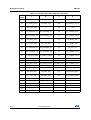
2.12
I/O header
All of the MCU GPIOs and communication channels can be accessed through a 4x37 I/O
headers. Here below the I/O header pin mapping summarized in .
18/24
DocID026329 Rev 1
UM1762
Hardware overview
Figure 28. I/O header (Schematic diagram)
("1(3*
Table 4. I/O header (Schematic diagram)
Pin
number
A
B
C
D
1
GND
GND
GND
+5V
2
D14_FlexPWM0_B1
G4_FlexPWM0_B2
E0_ADC1_AN5
E12_ADC1_AN10
3
G7_FlexPWM0_B3
D11_FlexPWM0_B0
C0_ADC1_AN3
E11_ADC1_AN9
4
B14_ADC1_AN1
E10_ADC1_AN8
B15_ADC1_AN2
E9_ADC1_AN7
5
E8_ADC1_AN6
D15_ADC1_AN4
--
E13_DSPI3_SCK
E14_DSPI3_SOU
T
E15_DSPI3_SIN
6
G8_FlexPWM0_FAU G9_FlexPWM0_FAU
LT0
LT1
7
G10_FlexPWM0_FA
ULT2
G11_FlexPWM0_FA
ULT3
--
--
8
F0_FlexRay0_DBG0 F1_FlexRay0_DBG1
--
--
9
C10_DSPI2_CS2
A9_DSPI2_CS1
--
C15_FlexRay0_CA_T
R_EN
10
A10_DSPI2_CS0
A11_DSPI2_SCK
--
D0_FlexRay0_CA_TX
11
A12_DSPI2_SOUT
A13_DSPI2_SIN
B2_LIN0_TXD
B3_LIN0_RXD
12
RESET
--
--
--
13
--
--
--
--
14
G0_FCU0_F0
--
NMI
D1_FlexRay0_CA_RX
DocID026329 Rev 1
19/24
23
Hardware overview
UM1762
Table 4. I/O header (Schematic diagram) (continued)
Pin
number
A
B
C
D
15
A5_DSPI1_CS0
A6_DSPI1_SCK
B1_CAN0_RXD
D2_FlexRay0_CB_RX
16
A7_DSPI1_SOUT
A8_DSPI1_SIN
17
B0_CAN0_TXD
18
D12_FlexPWM0_X1
G2_FlexPWM0_X2
A0_eTIMER0_ET
C0
A2_eTIMER0_ETC2
19
G5_FlexPWM0_X3
D9_FlexPWM0_X0
A1_eTIMER0_ET
C1
A4_eTIMER1_ETC0
20
C9_DSPI2_CS3
--
F11_NEXUS0_EV
TI
D8_DSPI1_CS2
21
F15_LIN1_RXD
F14_LIN1_TXD
F10_NEXUS0_EV
TO
C4_DSPI0_CS0
22
D13_FlexPWM0_A1
G3_FlexPWM0_A2
A3_eTIMER0_ET
C3
G1_FCU0_F1
23
G6_FlexPWM0_A3
D10_FlexPWM0_A0
C11_eTIMER0_ET
C13_eTIMER1_ETC1
C4
F2_FlexRay0_DBG2 F3_FlexRay0_DBG3
F9_NEXUS0_MSE
C14_eTIMER1_ETC2
O0
24
20/24
A15_SafetyPort0_
D3_FlexRay0_CB_TX
RXD
A14_SafetyPort0_TX C12_eTIMER0_ET D4_FlexRay0_CB_TR
D
C5
_EN
25
D7_DSPI1_CS3
C8_DSPI1_CS1
B6_CLKOUT
C5_DSPI0_SCK
26
B7_ADC0_AN0
B12_ADC0/1_AN14
C6_DSPI0_SOUT
C7_DSPI0_SIN
27
B13_ADC1_AN0
B11_ADC0/1_AN13
C3_DSPI0_CS1
F12_eTIMER1_ETC3
28
B10_ADC0/1_AN12
B9_ADC0/1_AN11
D6_DSPI0_CS2
F13_eTIMER1_ETC4
29
E2_ADC0_AN5
E7_ADC0_AN10
D5_DSPI0_CS3
F8_NEXUS0_MSEO1
30
B8_ADC0_AN1
E6_ADC0_AN9
F7_NEXUS0_MC
KO
F6_NEXUS0_MDO1
31
C2_ADC0_AN3
E5_ADC0_AN8
F5_NEXUS0_MD
O2
F4_NEXUS0_MDO3
32
E4_ADC0_AN7
C1_ADC0_AN2
GND
GND
33
E3_ADC0_AN6
E1_ADC0_AN4
+5V
5V
34
GND
GND
GND
5V
35
--
--
--
--
36
--
--
--
--
37
V_EXT_P
V_EXT_P
3v3
VDD_LV_COR
DocID026329 Rev 1
UM1762
3
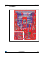
PCB layout
PCB layout
Figure 29. PCB layout
("1(3*
DocID026329 Rev 1
21/24
23
General handling precautions
Appendix A
UM1762
General handling precautions
The following precautions are recommended when using the SPC560P-DISP:
22/24
•
Do not modify or manipulate the board when the USB or DC supply is connected to the
board.
•
Do not supply the board with a DC source higher than +12V.
•
Any equipment or tool used for any manipulation of the semiconductor devices or
board modification should be shielded and connected to ground.
•
The connectors and cables should be plugged and removed when the board is off.
•
It is suggested recommended to use antistatic tools.
DocID026329 Rev 1
UM1762
Revision history
Revision history
Table 5. Document revision history
Date
Revision
20-May-2014
1
Changes
Initial release.
DocID026329 Rev 1
23/24
23
UM1762
Please Read Carefully:
Information in this document is provided solely in connection with ST products. STMicroelectronics NV and its subsidiaries (“ST”) reserve the
right to make changes, corrections, modifications or improvements, to this document, and the products and services described herein at any
time, without notice.
All ST products are sold pursuant to ST’s terms and conditions of sale.
Purchasers are solely responsible for the choice, selection and use of the ST products and services described herein, and ST assumes no
liability whatsoever relating to the choice, selection or use of the ST products and services described herein.
No license, express or implied, by estoppel or otherwise, to any intellectual property rights is granted under this document. If any part of this
document refers to any third party products or services it shall not be deemed a license grant by ST for the use of such third party products
or services, or any intellectual property contained therein or considered as a warranty covering the use in any manner whatsoever of such
third party products or services or any intellectual property contained therein.
UNLESS OTHERWISE SET FORTH IN ST’S TERMS AND CONDITIONS OF SALE ST DISCLAIMS ANY EXPRESS OR IMPLIED
WARRANTY WITH RESPECT TO THE USE AND/OR SALE OF ST PRODUCTS INCLUDING WITHOUT LIMITATION IMPLIED
WARRANTIES OF MERCHANTABILITY, FITNESS FOR A PARTICULAR PURPOSE (AND THEIR EQUIVALENTS UNDER THE LAWS
OF ANY JURISDICTION), OR INFRINGEMENT OF ANY PATENT, COPYRIGHT OR OTHER INTELLECTUAL PROPERTY RIGHT.
ST PRODUCTS ARE NOT DESIGNED OR AUTHORIZED FOR USE IN: (A) SAFETY CRITICAL APPLICATIONS SUCH AS LIFE
SUPPORTING, ACTIVE IMPLANTED DEVICES OR SYSTEMS WITH PRODUCT FUNCTIONAL SAFETY REQUIREMENTS; (B)
AERONAUTIC APPLICATIONS; (C) AUTOMOTIVE APPLICATIONS OR ENVIRONMENTS, AND/OR (D) AEROSPACE APPLICATIONS
OR ENVIRONMENTS. WHERE ST PRODUCTS ARE NOT DESIGNED FOR SUCH USE, THE PURCHASER SHALL USE PRODUCTS AT
PURCHASER’S SOLE RISK, EVEN IF ST HAS BEEN INFORMED IN WRITING OF SUCH USAGE, UNLESS A PRODUCT IS
EXPRESSLY DESIGNATED BY ST AS BEING INTENDED FOR “AUTOMOTIVE, AUTOMOTIVE SAFETY OR MEDICAL” INDUSTRY
DOMAINS ACCORDING TO ST PRODUCT DESIGN SPECIFICATIONS. PRODUCTS FORMALLY ESCC, QML OR JAN QUALIFIED ARE
DEEMED SUITABLE FOR USE IN AEROSPACE BY THE CORRESPONDING GOVERNMENTAL AGENCY.
Resale of ST products with provisions different from the statements and/or technical features set forth in this document shall immediately void
any warranty granted by ST for the ST product or service described herein and shall not create or extend in any manner whatsoever, any
liability of ST.
ST and the ST logo are trademarks or registered trademarks of ST in various countries.
Information in this document supersedes and replaces all information previously supplied.
The ST logo is a registered trademark of STMicroelectronics. All other names are the property of their respective owners.
© 2014 STMicroelectronics - All rights reserved
STMicroelectronics group of companies
Australia - Belgium - Brazil - Canada - China - Czech Republic - Finland - France - Germany - Hong Kong - India - Israel - Italy - Japan Malaysia - Malta - Morocco - Philippines - Singapore - Spain - Sweden - Switzerland - United Kingdom - United States of America
www.st.com
24/24
DocID026329 Rev 1