1
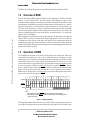
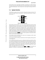
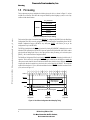
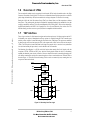
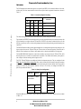
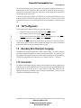
Freescale Semiconductor
Application Note
AN2387/D
Rev. 0, 11/2002
Freescale Semiconductor, Inc...
MPC8xx Using BDM and
JTAG
Robert McEwan
NCSD Applications
East Kilbride,
Scotland
As the technical complexity of microprocessors has increased, so too has the need for
adequate resources to enable efficient debugging and system testing. This application note
explains the functional and configurational differences between background debug mode
(BDM) and the IEEE 1149.1 test access port (TAP) of the MPC8xx device family. An
overview of each of the test mechanisms is followed by the basic operation and system
interfaces.
This document contains the following sections:
Topic
Section 1.1, “References”
Section 1.2, “Overview of BDM”
Section 1.3, “Operation of BDM”
Section 1.4, “System Interface”
Section 1.5, “Pin muxing”
Section 1.6, “Overview of JTAG”
Section 1.7, “TAP interface”
Section 1.8, “TAP Configuration”
Section 1.9, “Boundary Scan Descriptor Language”
Section 1.10, “Conclusion”
Appendix A, “Typical Set-up Questions and Answers”
1.1
Page
1
2
2
3
4
5
5
7
7
7
8
References
Users should familiarize themselves with the MPC860 PowerQUICC™ Family User Manual
(MPC860UM/D) and the Programming Environments Manual for 32-Bit Implementations of
the PowerPC™ Architecture, (MPEFPC32B/AD) .
These manuals can be downloaded from the MPC860 web-page:
Click on the link below to go to the Freescale Semiconductor Products Sector homepage:
http://www.freescale.com
Follow the links to:
Network and Communications Processors
© Freescale Semiconductor, Inc., 2004. All rights reserved.
For More Information On This Product,
Go to: www.freescale.com
Freescale Semiconductor, Inc.
Overview of BDM
The IEEE 1149.1 JTAG specification is also recommended reading for those unfamiliar with JTAG.
1.2
Overview of BDM
Freescale Semiconductor, Inc...
Before the introduction of BDM, the options available to users for debugging were limited to either ROM
monitors or in-circuit emulators (ICE). The former typically entails debugging code that has been
downloaded to RAM, requiring the same memory space as if burned into ROM. To communicate with the
external debugger, the ROM monitor also requires an interface that may be internal to the device, which can
degrade device performance, or an external interface, which increases board size. The other alternative, the
ICE, allows greater flexibility in the control of the processor including real-time tracing, programming
model access and hardware breakpoints, without using processor resources. However, since it requires the
bond-out of additional signals, along with external memory and specialized cables, it is considered an
expensive outlay for development.
BDM is implemented on the MPC8xx to overcome the limitations of the ROM monitor and without the
expense of ICE. This is achieved via some of the development support functions on the device, which will
be explained later in the document. A full-duplex serial interface, allows communications between the
development port support logic and the development tool. This allows program flow tracking, along with
internal watchpoint and breakpoint generation. More importantly, single step debugging allows memory and
registers to be examined at any point.
1.3
Operation of BDM
The development port can operate in two modes, either trap enable mode or debug mode. When in trap
enable mode the development port receives a 10 bit transmission from the development tool. These
transmissions are used to control the on-chip breakpoint functions and the debug port commands. In debug
mode all (32-bit) instructions are fetched from the development port and are fed into the processor to be
executed, with load/store accesses performed on the real system memory. Debug mode operation is enabled
at reset by the assertion of DSCK at least three clocks before the negation of SRESET, as shown in
Figure 1-1. If DSCK is then asserted past the SRESET negation, the processor takes a breakpoint exception
and goes directly into debug mode instead of fetching the reset vector. This allows the user to debug a
ROM-less system. If debug mode is not required directly after reset then DSCK must be negated no later
than seven clock cycles after the negation of SRESET.
0
1
2
3
4
5
6
7
8
9
10
11 12
13 14 15
16 17
CLKOUT
SRESET
DSCK
Note 1
Note 2
Notes:
1. DSCK asserts high while SRESET asserted to enable debug mode operation.
2. DSCK asserts high after SRESET negation to enter debug mode immediately (without
fetching reset vector).
Figure 1-1. Debug mode entry
The Debug Enable Register (DER) allows the user to selectively enable events that cause the processor to
enter debug mode. Interrupt events are reported in the Interrupt Cause Register (ICR). This results in entry
2
MPC8xx Using BDM and JTAG
For More Information On This Product,
Go to: www.freescale.com
Freescale Semiconductor, Inc.
System Interface
into debug mode only if the corresponding bit in the DER is set and debug mode is enabled. After debug
mode entry, program execution will continue from the point at which debug mode was entered. To exit from
debug mode use the rfi instruction. This returns the processor to normal operation and negates the FRZ/FLS
pins.
1.4
System Interface
Freescale Semiconductor, Inc...
The BDM signals communicate with the development tool through the development port interface. This
consists of several pins on the device that are routed to a 10-pin dual-row header on the user’s board, as
shown in Figure 1-2.
FRZ/VFLS0
1
2
SRESET
GND
3
4
DSCK
GND
5
6
FRZ/VFLS1
HRESET
7
8
DSDI
VDD
9
10
DSDO
Figure 1-2. BDM connector Pinout
The Development Serial Clock (DSCK) is used at reset to enable debug mode. This can be entered either
immediately following reset or on the occurrence of an event reported in the ICR. DSCK is an input to the
development port and must be driven either high or low at all times. It must not be allowed to float. It is
therefore recommended to connect this pin to a pull-down resistor to prevent accidental entry to debug
mode. The DSCK is also used to clock the data in and out of the development port shift register, when in
asynchronous clocked mode, so called because DSCK is asynchronous with CLKOUT. Another clock mode
available, called synchronous self-clocked, does not require the input clock. Instead, the port is clocked via
the system clock. The selection between these two clock modes occurs at reset. The DSDI input is latched
eight clocks after the negation of SRESET. If the input is low, then asynchronous clocked mode is enabled,
otherwise synchronous self-clocked mode is enabled.
The Development Serial Data In (DSDI) pin receives data from the development tool, which is shifted
serially into the development port shift register.
The Development Serial Data Out (DSDO) pin transmits data out of the development port shift register back
to the development tool.
The Freeze (FRZ) pin indicates that the processor is in debug mode, which can be used to halt any off-chip
device and allows a handshake between the development port and tool. When the FRZ signal is asserted, the
clocks to the software watchdog, PIT, real-time clock, timebase counter, and decrementer can be disabled.
This is controlled by the associated bits in the control register of each timer. If they are programmed to stop
counting when FRZ is asserted, the counters maintain their values until FRZ is negated. However, the bus
monitor, will be enabled regardless of the state of this signal.
To allow the development tool to reset the processor, both HRESET and SRESET must be included on the
BDM header. The VDD pin is also required and provides a power sense to the development tool.
MPC8xx Using BDM and JTAG
For More Information On This Product,
Go to: www.freescale.com
3
Freescale Semiconductor, Inc.
Pin muxing
1.5
Pin muxing
The development port pins are multiplexed with other pins on the device, as shown in Figure 1-3, and are
available in two locations. This allows the user greater flexibility when designing a system, in case of any
conflict with the shared function.
ALE_B/DSCK/AT1
IP_B6/DSDI/AT0
OP3/MODCK2/DSDO
MPC8xx
TCK/DSCK
TDI/DSDI
Freescale Semiconductor, Inc...
TDO/DSDO
Figure 1-3. Development Port pin-muxing
The location of these pins is determined during HRESET by configuring the [DBPC] bits in the Hard Reset
Configuration Word. After reset the configuration set-up is loaded into the corresponding bits of the SIU
Module Configuration Register (SIUMCR). Any subsequent SRESET will load the pin as per the
configuration set-up in the SIUMCR.
The FRZ pin is multiplexed with IRQ6 and is selected by clearing SIUMCR[FRC], although the reset value
defaults to FRZ. Optionally, the VFLS0/VFLS1 pins can replace the FRZ pin and the value of 0b11 on these
pins also indicates debug mode. However, since these pins also share pin muxing, to be selected requires
[DBGC] = 0b11 in the Hard Reset Configuration Word.
The Hard Reset Configuration Word is used during a PORESET/ HRESET to determine the initial mode of
operation. This is achieved by asserting the RSTCONF signal, which instructs the MPC8xx to sample the
values present on the data-bus, otherwise the internal default value (0x00) is selected. When the PORESET
is negated, the data-bus is sampled every nine clock cycles, on the rising edge of CLKOUT. The set-up time
required for the data bus is 15 cycles, while the maximum rise time of HRESET should be less than six clock
cycles, as shown in Figure 1-4.
0
1
2
3
4
5
6
7
8
9
10
11 12
13 14
15 16 17
CLKOUT
HRESET
Maximum time of
reset recognition
RSTCONF
DATA
Reset configuration word
Maximum set-up time of reset recognition
Sample data
configuration
Sample data
configuration
Figure 1-4. Hard Reset Configuration Word Sampling Timing
4
MPC8xx Using BDM and JTAG
For More Information On This Product,
Go to: www.freescale.com
Sample data
configuration
Freescale Semiconductor, Inc.
Overview of JTAG
1.6
Overview of JTAG
The conventional methods used to test printed circuit boards (PCBs) involved methods such as the Edge
Connector Test and the “Bed of Nails” Test. However, with introduction of high pin-count devices with fine
pitch, along with multi-layer PCBs, these methods are no longer adequate or cost-effective in testing.
During the 1980’s the Joint Test Action Group (JTAG) was formed from over 200 companies to address
these issues. They subsequently developed a standard for integrating hardware into standard devices, that
could be controlled by software. This was termed Boundary Scan Testing (BST). This was later adopted by
the IEEE and defined as the IEEE 1149.1 Standard Test Access Port and Boundary Scan Architecture. The
MPC8xx family provides a test access port (TAP) that is compatible with this standard.
Freescale Semiconductor, Inc...
1.7
TAP interface
The test logic consists of a 4-bit instruction register and two data registers (a 1-bit bypass register and a 475
bit boundary scan register). Manipulation of these registers is controlled using the TAP controller state
machine, whose sequence is controlled using the Test mode select (TMS) input. The registers are modified
by data from the serial test data input pin (TDI), with output results visible on the serial test data out pin
(TDO). The TDO pin is tri-stated when data is not being driven out the device. An active low asynchronous
reset (with an internal pull-up resistor) is used to initialize the TAP controller.
The Boundary Scan Register is a 475-bit serial shift register that contains bits for all signals, with the
exception of XTAL, EXTAL and XFC pins, which are analog signals. When the device is functioning
normally the boundary scan circuitry is inactive. However when the test mode is entered the boundary scan
cells that are contained in each pin are connected together to form a scan chain between TDI and TDO, as
shown in Figure 1-5. This allows electrical testing of devices such as connectivity tests, ensuring there are
no opens or shorts on the board.
TRST
TMS
TCK
TAP
controller
Instruction
register
TDI
Inputs
Bypass
register
Core
logic
TDO
Outputs
Boundary scan register
Figure 1-5. Boundary Scan Test Logic
MPC8xx Using BDM and JTAG
For More Information On This Product,
Go to: www.freescale.com
5
Freescale Semiconductor, Inc.
TAP interface
The TAP implements an instruction register, as required by the IEEE 1149.1 standard, which is 4-bits wide,
with no parity. The four instruction bits select the three required and two optional instructions as shown in
Table 1-1.
Table 1-1. Instruction Register Decoding
Code
Freescale Semiconductor, Inc...
Instruction
B3
B2
B1
B0
0
0
0
0
EXTEST
0
0
0
1
SAMPLE/PRELOAD
0
X
1
X
BYPASS
0
1
0
0
HI-Z
0
1
0
1
CLAMP & BYPASS
The instruction register selects the BYPASS instruction by default, during the test-logic-reset state.
The external test (EXTEST) instruction places the device into external boundary test mode and connects the
475-bit boundary scan register between TDI and TDO. EXTEST also asserts an internal soft reset for the
MPC8xx system logic to force to a known beginning internal state while performing external boundary scan
operations.
The BYPASS instruction allows data to pass through the device during normal operation by placing the 1-bit
bypass register between the TDI and TDO pins. The data does not enter the boundary scan chain and is
therefore used to enhance test efficiency when another device, other than the MPC8xx is being tested.
The SAMPLE/PRELOAD instruction connects the boundary scan register between TDI and TDO, while
allowing the device to remain in its normal mode of operation. This enables the boundary scan register to
take a sample of the data entering and leaving the device.
The TCK, TDI and TDO pins are multiplexed with the development port pins. They are configured in the
DBPC bits of the Hard Reset Configuration Word, which is loaded from the data bus, during the assertion
of HRESET and RSTCONF. If RSTCONF is not asserted during this time the default value of 0x0 will be
selected. To ensure the TAP interface functions correctly it is necessary to configure the DBPC bits
[D11/D12] as shown in Table 1-2
Table 1-2. Debug Port Configuration
DBPC=00
DBPC=01
De ned b y DBGC.
Note: If DPBC = 11, DPBC
overrides DBGC.
DBPC=10
Reserved
DPBC=11
DSCK
DSDI
DSDO
PTR*
DSCK
TCK
TCK
DSDI
TDI
TDI
DSDO
TDO
TDO
If both the BDM and TAP ports are required then DPBC must be set to 0x11, as shown in the last column
of Table 1-2.
6
MPC8xx Using BDM and JTAG
For More Information On This Product,
Go to: www.freescale.com
Freescale Semiconductor, Inc.
TAP Configuration
The TAP controller remains in the test-logic-reset state after power-on and is disabled to allow the device to
function normally. To enter JTAG mode set TMS=0. The default on entering JTAG mode is for the core to
come up in a state equivalent to BYPASS mode. In this mode a 1bit shift register path is created between
TDI, through the bypass register to TDO.
A simple way to indicate that the MPC8xx is in JTAG mode is to enter the default BYPASS mode, clock a
bit stream into TDI and monitor the bit stream coming back out on TDO 1 cycle later. Assertion of FRZ
signal indicates that the core is in debug mode and therefore the entry conditions for JTAG have not been
met.
1.8
TAP Configuration
Freescale Semiconductor, Inc...
The TAP signals must be configured as follows to reset the scan chain logic:
•
•
•
If both the TAP and low power mode are never used, connect TRST to ground.
If the TAP or low power mode is used, connect TRST to PORESET.
If power down mode (the lowest power mode, where VDDH is disabled) is used, connect TRST to
PORESET through a diode (anode to TRST, cathode to PORESET).
The TMS, TDI, and TRST signals include on-chip pull-up resistors. However, TCK does not have an
on-chip pull-up or pull-down resistor; it should be pulled down through a (10k) resistor. TCK should not
be greater than 10MHz since this is the maximum frequency allowed.
1.9
Boundary Scan Descriptor Language
The Boundary Scan Descriptor Language (BSDL), which is a subset of VHDL, was devised to standardize
the method of describing the boundary-scan architectures detailed in the IEEE 1149.1 specification. This
allows designers and test software developers to generate test patterns and perform in-circuit programming.
The BSDL file for the MPC860 can be found on the web, as described in Section 1.1, “References”.
1.10 Conclusion
The challenges of the debugging and testing of high pin count microprocessors on densely populated circuit
boards have been overcome on the MPC8xx devices. This has been achieved by integrating BDM and JTAG
support functions on silicon with access via a simple interface for each. These features are easily
implemented without taking up valuable board space, resulting in increased efficiency in the user’s system
development, while simultaneously reducing cost.
MPC8xx Using BDM and JTAG
For More Information On This Product,
Go to: www.freescale.com
7
Freescale Semiconductor, Inc.
Typical Set-up Questions and Answers
Appendix A
Typical Set-up Questions and Answers
The following questions are frequently asked during the set-up phase.
When the 8xx is in BDM, if the cache is enabled, will the cache respond to accesses to external memory?
That is, if you try to read/write memory from the core when in BDM, will caches intervene and respond?
When you are in BDM, caches are frozen. You can read/write the registers of the cache, and
thereby look into it, but the cache will not try to operate in its normal fashion. This is true
regardless of the mode that the cache was in before entry into BDM.
Freescale Semiconductor, Inc...
Can the FRZ signal pin be substituted in place of VFLS(0:1) on MPC8xx BDM interface without affecting
debug mode functionality?
If you don't plan on using the trace function, then you don't need the VFLS pins. FRZ is not a
substitute for VFLS, their function (as described in the Development Support section of the
User Manual) is completely different.
In BDM, while accessing memory, is the device’s operation is stopped?
In BDM the MPC8xx core is held in a frozen state and will only accept instructions from the
BDM port. If no instructions are issued the core remains frozen i.e. it's operation is stopped until
the next instruction appears on the BDM port. The MPC8xx should not fall over in the middle
of a memory access. If the cycle completes for example writing to internal memory and there
is no more instructions to process the processor will stop.
Do the instructions that come from the development port use physical addresses instead of logical
addresses. The user manual indicates that instructions from development port perform accesses on the real
system memory. Does it mean physical memory?
Physical addressed memory is referred to as real addresses in the architecture specification.
What happens after a Soft reset (SRESET)?
When a soft reset event occurs the MPC8xx will reconfigure the development port, depending
on the user’s settings.. The user should ensure there are no spurious writes to the SIUMCR that
could corrupt the debug port / pin configurations.
How should the TAP be configured to prevent accidental entry to JTAG?
To ensure that the scan chain test logic is kept transparent to the system logic during normal
operation, the TAP should be forced into the test-logic-reset controller state by keeping TRST
or TMS continuously asserted.
If the MPC8xx starts executing from FLASH after power-up and enters JTAG mode, will it continue to
execute the code from FLASH?
This depends on which state the JTAG port is configured in coming out of reset. When the
BYPASS mode of operation is selected, all of the test registers in the MPC8xx perform their
normal system function.
What will the core of the MPC8xx do when it is in JTAG mode?
The default on entering JTAG mode is for the core to come up in a state equivalent to BYPASS
mode. In this mode a 1bit shift register path is created between TDI, through the bypass register
to TDO. A simple way to indicate that the MPC8xx is in JTAG mode is to enter the default
BYPASS mode, clock a bit stream into TDI and monitor the bit stream coming back out on
TDO 1 cycle later.
8
MPC8xx Using BDM and JTAG
For More Information On This Product,
Go to: www.freescale.com
Freescale Semiconductor, Inc.
Typical Set-up Questions and Answers
Is assertion of FRZ expected in JTAG mode?
Assertion of FRZ signal indicates that the core is in debug mode and therefore the entry
conditions for JTAG have not been met.
If SIUMCR [DBGC and DBPC] are latched during the PORESET can they be modified afterwards by
software?
The user can write to these fields at any time as long as SIUMCR[DLK] is not asserted.
TRST must be asserted at least initially to set up JTAG. If TRST remains low, can JTAG still be used by
pulling TMS to 0 and clocking TCK?
TRST cannot remain low, but must be pulled low initially.
Freescale Semiconductor, Inc...
Will JTAG work if the clock input to the processor is held inactive? Will the PLL never lock?
Boundary scan testing should still be possible with the clock input to the processor held inactive
- its operation decouples the processor system clock prior to testing. However, any non-scan
testing the user plans to do such as checking registers, will require some form of clock
functionality. If the PLL experiences a loss of lock (PLPRCR[LOLRE]=1) an internal hard
reset will occur. If the user to attempts to start the processor clock from this inactive state, they
should not expect the PLL to function correctly. It requires stable input clocks to operate.
Is the software watchdog disabled in BDM and JTAG mode?
The software watchdog configuration will be the same as was set up in the system protection
control register SYPCR[SWE], when JTAG is enabled. The user will need to take into account
any resets to the MPC8xx as JTAG is entered. The watchdog timer has to be disabled manually.
The same applies to BDM. Out of reset, if JTAG is enabled and is being used for board testing,
i.e. continuity testing, and not to monitor the chip internals, then the fact that the Watchdog
times out and HRESET is asserted should not matter.
MPC8xx Using BDM and JTAG
For More Information On This Product,
Go to: www.freescale.com
9
Freescale Semiconductor, Inc.
Freescale Semiconductor, Inc...
Typical Set-up Questions and Answers
10
MPC8xx Using BDM and JTAG
For More Information On This Product,
Go to: www.freescale.com
Freescale Semiconductor, Inc.
Freescale Semiconductor, Inc...
Typical Set-up Questions and Answers
MPC8xx Using BDM and JTAG
For More Information On This Product,
Go to: www.freescale.com
11
Freescale Semiconductor, Inc.
How to Reach Us:
Home Page:
www.freescale.com
Freescale Semiconductor, Inc...
E-mail:
[email protected]
USA/Europe or Locations Not Listed:
Freescale Semiconductor
Technical Information Center, CH370
1300 N. Alma School Road
Chandler, Arizona 85224
+1-800-521-6274 or +1-480-768-2130
[email protected]
Europe, Middle East, and Africa:
Freescale Halbleiter Deutschland GmbH
Technical Information Center
Schatzbogen 7
81829 Muenchen, Germany
+44 1296 380 456 (English)
+46 8 52200080 (English)
+49 89 92103 559 (German)
+33 1 69 35 48 48 (French)
[email protected]
Japan:
Freescale Semiconductor Japan Ltd.
Headquarters
ARCO Tower 15F
1-8-1, Shimo-Meguro, Meguro-ku,
Tokyo 153-0064
Japan
0120 191014 or +81 3 5437 9125
[email protected]
Asia/Pacific:
Freescale Semiconductor Hong Kong Ltd.
Technical Information Center
2 Dai King Street
Tai Po Industrial Estate
Tai Po, N.T., Hong Kong
+800 2666 8080
[email protected]
For Literature Requests Only:
Freescale Semiconductor Literature Distribution Center
P.O. Box 5405
Denver, Colorado 80217
1-800-441-2447 or 303-675-2140
Fax: 303-675-2150
[email protected]
Information in this document is provided solely to enable system and software
implementers to use Freescale Semiconductor products. There are no express or
implied copyright licenses granted hereunder to design or fabricate any integrated
circuits or integrated circuits based on the information in this document.
Freescale Semiconductor reserves the right to make changes without further notice to
any products herein. Freescale Semiconductor makes no warranty, representation or
guarantee regarding the suitability of its products for any particular purpose, nor does
Freescale Semiconductor assume any liability arising out of the application or use of
any product or circuit, and specifically disclaims any and all liability, including without
limitation consequential or incidental damages. “Typical” parameters which may be
provided in Freescale Semiconductor data sheets and/or specifications can and do
vary in different applications and actual performance may vary over time. All operating
parameters, including “Typicals” must be validated for each customer application by
customer’s technical experts. Freescale Semiconductor does not convey any license
under its patent rights nor the rights of others. Freescale Semiconductor products are
not designed, intended, or authorized for use as components in systems intended for
surgical implant into the body, or other applications intended to support or sustain life,
or for any other application in which the failure of the Freescale Semiconductor product
could create a situation where personal injury or death may occur. Should Buyer
purchase or use Freescale Semiconductor products for any such unintended or
unauthorized application, Buyer shall indemnify and hold Freescale Semiconductor
and its officers, employees, subsidiaries, affiliates, and distributors harmless against all
claims, costs, damages, and expenses, and reasonable attorney fees arising out of,
directly or indirectly, any claim of personal injury or death associated with such
unintended or unauthorized use, even if such claim alleges that Freescale
Semiconductor was negligent regarding the design or manufacture of the part.
AN2387/D
For More Information On This Product,
Go to: www.freescale.com