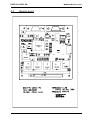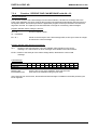
1
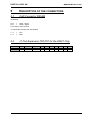
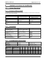
TECHNICAL USER'S MANUAL FOR: PC/104 Peripheral boards MSMCAN CAN-BUS interface card #260399-1 Nordstrasse 11/F, CH-4542 Luterbach Tel.: ++41 (0)32 681 53 33 - Fax: ++41 (0)32 681 53 31 DIGITAL-LOGIC AG MSMCAN Manual V1.60b COPYRIGHT 1992-95 BY DIGITAL-LOGIC AG No part of this document may be reproduced, transmitted, transcribed, stored in a retrieval system, in any form or by any means, electronic, mechanical, optical, manual, or otherwise, without the prior written permission of DIGITAL-LOGIC AG. The software described herein, together with this document, are furnished under a license agreement and may be used or copied only in accordance with the terms of that agreement. REVISION HISTORY: Prod.-Serialnumber: From: To: Product Version V1.4B V1.4B V1.4B V1.4B BETA Document Version V1.1 V1.2 V1.3 V1.4 V1.5 V1.51 V1.52 V1.60b 2 Date/Visa: 02.95 FK 07.95 FK 09.96 RP 09.96 RP 10.96 RP 12.97 SL 03.99 TS 03.99 JM Modification: Remarks, News, Attention: Initial Version Current Version New Structure Jumper Function 04, 05, Revision Write to register, sample rev. Related APP-NOTES Maintenance update DIGITAL-LOGIC AG MSMCAN Manual V1.60b Registration Form: Please register your product under: http://www.digitallogic.ch -> SUPPORT -> Product Registration After registration, you will receive driver & software updates, errata information, customer information and news from DIGITAL-LOGIC AG products automatically. 3 DIGITAL-LOGIC AG MSMCAN Manual V1.60b Table of Contents 1 PREFACE............................................................................................................................ 6 1.1 1.2 1.3 1.4 1.5 1.6 1.7 2 How to use this manual...................................................................................................................6 Trademarks .....................................................................................................................................6 Disclaimer .......................................................................................................................................6 Who should use this product...........................................................................................................6 Recycling information ......................................................................................................................7 Technical Support ...........................................................................................................................7 Limited Warranty.............................................................................................................................7 OVERVIEW ......................................................................................................................... 8 2.1 2.2 2.3 Standard Features ..........................................................................................................................8 Ordering Information .......................................................................................................................8 Related Application Notes ...............................................................................................................8 3 PC/104 BUS SIGNALS........................................................................................................ 9 4 DETAIL SYSTEM DESCRIPTION ..................................................................................... 12 4.1 5 82527 Controller............................................................................................................................12 DESCRIPTION OF THE CONNECTORS .......................................................................... 13 5.1 5.2 5.3 6 CAN Connector DSUB9 ................................................................................................................13 J7 Port Expansion P20-P27 for the 82527 Chip ...........................................................................13 J40 PC/104 BUS Interface ............................................................................................................14 JUMPER LOCATIONS ON THE BOARD .......................................................................... 15 6.1 Jumper Descriptions .....................................................................................................................15 6.1.1 IO-mapped or Memory-mapped.............................................................................................15 6.1.2 PLD Equations .......................................................................................................................15 6.1.3 S1 IO-BASE-Address Selection Switch .................................................................................15 6.1.4 S2 IRQ Selector Switch .........................................................................................................16 6.1.5 S3 NODE Selector Switch .....................................................................................................16 6.2 Board Layout .................................................................................................................................17 7 SOFTWARE ...................................................................................................................... 18 7.1 7.2 7.2.1 7.2.2 7.3 7.3.1 7.3.2 7.3.3 7.3.4 7.3.5 7.3.6 7.4 8 Delivered Software ........................................................................................................................18 Accessing the CAN-Controller 82527 from Intel ...........................................................................18 IO-mapped Operation ............................................................................................................18 MEMORY-mapped Operation ................................................................................................19 Functions of the CAN-Driver .........................................................................................................19 Function: INIT CAN with AH = 00 .........................................................................................19 Function: TRANSMIT CAN MESSAGE with AH = 01 ...........................................................20 Function: READY CAN with AH = 02....................................................................................20 Function: RECEIVE ONE CAN MESSAGE with AH = 03.....................................................21 Function: CAN_RxDADR with AH = 4 * ..............................................................................22 Function: Get_Status Register with AH = 5 ..........................................................................22 Program Example in Pascal..........................................................................................................24 BUILDING A SYSTEM ...................................................................................................... 26 8.1 8.2 8.2.1 8.3 8.4 CAN Bus cable and termination ....................................................................................................26 To start the CAN card ...................................................................................................................26 Installation of the CAN-Driver CA_I9.COM or CA_I5.COM ...................................................26 The CANTEST.EXE Program to monitor the CAN bus.................................................................27 Uninstalling the CAN-Driver CA........COM ....................................................................................29 4 DIGITAL-LOGIC AG 9 MSMCAN Manual V1.60b DIAGNOSTICS .................................................................................................................. 30 9.1 General..........................................................................................................................................30 10 FAILURES AND HINTS.................................................................................................. 31 10.1 10.2 11 CAN does not work .......................................................................................................................31 500 kBit/s Speed Problem.............................................................................................................31 INDEX ............................................................................................................................ 32 5 DIGITAL-LOGIC AG 1 MSMCAN Manual V1.60b PREFACE This manual is for integrators and programmers of systems based on the MICROSPACE card family. It contains information on hardware requirements, interconnections, and details of how to program the system. The specifications given in this manual were correct at the time of printing; advances mean that some may have changed in the meantime. If errors are found, please notify DIGITAL-LOGIC AG at the address shown on the title page of this document, and we will correct them as soon as possible. 1.1 How to use this manual This manual is written for the original equipment manufacturer (OEM) who plans to build computer systems based on the single board MICROSPACE-PC. It provides instructions for installing and configuring MICROSPACE boards, and describes the system and setup requirements. 1.2 Trademarks Chips & Technologies MICROSPACE, MicroModule DOS Vx.y, Windows PC-AT, PC-XT NetWare Ethernet DR-DOS, PALMDOS ROM-DOS 1.3 SuperState R DIGITAL-LOGIC AG Microsoft Inc. IBM Novell Corporation Xerox Corporation Digital Research Inc. / Novell Inc. Datalight Inc. Disclaimer DIGITAL-LOGIC AG makes no representations or warranties with respect to the content of this manual and specifically disclaims any implied warranty of merchantability or fitness for any particular purpose. DIGITAL-LOGIC AG shall under no circumstances be liable for incidental or consequential damages or related expenses resulting from the use of this product, even if it has been notified of the possibility of such damage. DIGITAL-LOGIC AG reserves the right to revise this publication from time to time without obligation to notify any person of such revisions. If errors are found, please contact DIGITAL-LOGIC AG at the address listed on the title page of this document. 1.4 - Who should use this product Electronic engineers with know-how in PC-technology. Without electronic know-how we expect you to have questions. This manual assumes, that you have a general knowledge of PC-electronics. Because of the complexity and the variability of PC-technology, we can’t give any warranty that the product will work in any particular situation or combination. Our technical support will help you. Pay attention to the electrostatic discharges. Use a CMOS protected workplace. Power supply OFF when you are working on the board or connecting any cables or devices. This is a high-technology product. You need know-how in electronics and PC-technology to install the system ! 6 DIGITAL-LOGIC AG 1.5 MSMCAN Manual V1.60b Recycling information Hardware: - Print: epoxy with glass fiber wires are of tin-plated copper - Components: ceramics and alloys of gold, silver check your local electronic recycling Software: - no problems: re-use the diskette after formatting 1.6 Technical Support 1. Contact your local Digital-Logic Technical Support in your country. 2. Use Internet Support Request form on http://www.digitallogic.ch -> support 3. Send a FAX or an E-mail to DIGITAL-LOGIC AG with a description of your problem. DIGITAL-LOGIC AG Dept. Tech. Support Nordstr. 4F CH-4542 Luterbach (SWITZERLAND) Fax: ++41-32 681 53 31 E-Mail: [email protected] è Support requests will only be accepted with detailed informations about the product (BIOS, Board Version) ! 1.7 Limited Warranty DIGITAL-LOGIC AG warrants the hardware and software products it manufactures and produces to be free from defects in materials and workmanship for one year following the date of shipment from DIGITAL-LOGIC AG, Switzerland. This warranty is limited to the original product purchaser and is not transferable. During the one year warranty period, DIGITAL-LOGIC AG will repair or replace, at its discretion, any defective product or part at no additional charge, provided that the product is returned, shipping prepaid, to DIGITAL-LOGIC AG. All replaced parts and products become property of DIGITAL-LOGIC AG. Before returning any product for repair, customers are required to contact the company. This limited warranty does not extend to any product which has been damaged as a result of accident, misuse, abuse (such as use of incorrect input voltages, wrong cabling, wrong polarity, improper or insufficient ventilation, failure to follow the operating instructions that are provided by DIGITAL-LOGIC AG or other contingencies beyond the control of DIGITAL-LOGIC AG), wrong connection, wrong information or as a result of service or modification by anyone other than DIGITAL-LOGIC AG. Neither, if the user has not enough knowledge of these technologies or has not consulted the product manual or the technical support of DIGITAL-LOGIC AG and therefore the product has been damaged. Except, as expressly set forth above, no other warranties are expressed or implied, including, but not limited to, any implied warranty of merchantability and fitness for a particular purpose, and DIGITAL-LOGIC AG expressly disclaims all warranties not stated herein. Under no circumstances will DIGITAL-LOGIC AG be liable to the purchaser or any user for any damage, including any incidental or consequential damage, expenses, lost profits, lost savings, or other damages arising out of the use or inability to use the product. 7 DIGITAL-LOGIC AG MSMCAN Manual V1.60b 2 OVERVIEW 2.1 Standard Features Controller: Clock: Intel 82527 16MHz CAN Specification: V2.0 part B Frames: Identifier: Objects: Standard and extended data and remote frames Standard and extended message identifier 14 TX/RX objects and 1 Rx object with programmable mask Host Interface: IO-mapped or memory-mapped 1k window C800,CC00, D000, D400, D800, DC00 200h to 3ffh I/O range CAN Interface: Driver Output: CAN Speed: Protection: Standard ISO/DIS 11898 50 mA up to 500 kBaud Thermal shutdown Power Supply: Bus: Size: Environmental Temperature: 5V PC/104 104 stackthrough pins 96 x 90 mm operating: -25°C to + 85°C storage: - 65°C to +125°C 9 pin DSub Any information is subject to change without notice. 2.2 Ordering Information MSMCAN MICROSPACE PC/104 CAN Controller 2.3 Related Application Notes # 19A 30 72 Description For MSMCAN and other CAN-Products CAN Software CAN 82C527 Controller è Application Notes are availble at http://www.digitallogic.ch ->support, or on any Application CD from DIGITAL-LOGIC. 8 DIGITAL-LOGIC AG 3 MSMCAN Manual V1.60b PC/104 BUS SIGNALS AEN, output Address Enable is used to degate the microprocessor and other devices from the I/O channel to allow DMA transfers to take place. low = CPU Cycle , high = DMA Cycle BALE, output Address Latch Enable is provided by the bus controller and is used on the system board to latch valid addresses and memory decodes from the microprocessor. This signal is used so that devices on the bus can latch LA17..23. The SA0..19 address lines latched internally according to this signal. BALE is forced high during DMA cycles. /DACK[0..3, 5..7], output DMA Acknowledge 0 to 3 and 5 to 7 are used to acknowledge DMA requests (DRQO through DRQ7). They are active low. This signal indicates that the DMA operation can begin. DRQ[0..3, 5..7], input DMA Requests 0 through 3 and 5 through 7 are asynchronous channel requests used by peripheral devices and the I/O channel microprocessors to gain DMA service (or control of the system). A request is generated by bringing a DRQ line to an active level. A DRQ line must be held high until the corresponding DMA Request Acknowledge (DACK/) line goes active. DRQO through DRQ3 will perform 8-Bit DMA transfers; DRQ5-7 are used for 16 accesses. /IOCHCK, input IOCHCK/ provides the system board with parity (error) information about memory or devices on the I/O channel. low = parity error, high = normal operation IOCHRDY, input I/O Channel Ready is pulled low (not ready) by a memory or I/O device to lengthen I/O or memory cycles. Any slow device using this line should drive it low immediately upon detecting its valid address and a Read or Write command. Machine cycles are extended by an integral number of one clock cycle (67 nanoseconds). This signal should be held low for no more than 2.5 microseconds. low = wait, high = normal operation /IOCS16, input I/O 16 Bit Chip Select signals the system board that the present data transfer is a 16-Bit, 1 wait-state, I/0 cycle. It is derived from an address decode. /IOCS16 is active low and should be driven with an open collector (300 ohm pull-up) or tri-state driver capable of sinking 20mA. The signal is driven based only on SA15-SAO (not /IOR or /IOW) when AEN is not asserted. In the 8 Bit I/O transfer, the default transfers a 4 wait-state cycle. /IOR, input/output I/O Read instructs an I/O device to drive its data onto the data bus. It may be driven by the system microprocessor or DMA controller, or by a microprocessor or DMA controller resident on the I/O channel. This signal is active low. /IOW, input/output I/O Write instructs an I/O device to read the data on the data bus. It may be driven by any microprocessor or DMA controller in the system. This signal is active low. 9 DIGITAL-LOGIC AG MSMCAN Manual V1.60b IRQ[ 3 - 7, 9 - 12, 14, 15], input These signals are used to tell the microprocessor that an I/O device needs attention. An interrupt request is generated when an IRQ line is raised from low to high. The line must be held high until the microprocessor acknowledges the interrupt request. /Master, input This signal is used with a DRQ line to gain control of the system. A processor or DMA controller on the I/0 channel may issue a DRQ to a DMA channel in cascade mode and receive a /DACK. /MEMCS16, input MEMCS16 Chip Select signals the system board if the present data transfer is a 1 wait-state, 16-Bit, memory cycle. It must be derived from the decode of LA17 through LA23. /MEMCS16 should be driven with an open collector (300 ohm pull-up) or tri-state driver capable of sinking 2OmA. /MEMR input/output These signals instruct the memory devices to drive data onto the data bus. /MEMR is active on all memory read cycles. /MEMR may be driven by any microprocessor or DMA controller in the system. When a microprocessor on the I/0 channel wishes to drive /MEMR, it must have the address lines valid on the bus for one system clock period before driving /MEMR active. These signals are active low. /MEMW, input/output These signals instruct the memory devices to store the data present on the data bus. /MEMW is active in all memory read cycles. /MEMW may be driven by any microprocessor or DMA controller in the system. When a microprocessor on the I/O channel wishes to drive /MEMW, it must have the address lines valid on the bus for one system clock period before driving /MEMW active. Both signals are active low. OSC, output Oscillator (OSC) is a high-speed clock with a 70 nanosecond period (14.31818 MHz). This signal is not synchronous with the system clock. It has a 50% duty cycle. OSC starts 100µs after reset is inactive. RESETDRV, output Reset Drive is used to reset or initiate system logic at power-up time or during a low line-voltage outage. This signal is active high. When the signal is active all adapters should turn off or tri-state all drivers connected to the I/O channel. This signal is driven by the permanent Master. /REFRESH, input/output These signals are used to indicate a refresh cycle and can be driven by a microprocessor on the I/0 channel. These signals are active low. SAO-SA19, LA17 - LA23 input/output Address bits 0 through 19 are used to address memory and I/0 devices within the system. These 20 address lines, allow access of up to 1 MBytes of memory. SAO through SA19 are gated on the system bus when BALE is high and are latched on the falling edge of BALE. LA17 to LA23 are not latched and addresses the full 16 Mbytes range. These signals are generated by the microprocessors or DMA controllers. They may also be driven by other microprocessor or DMA controllers that reside on the I/0 channel. The SA17-SA23 are always LA17-LA23 address timings for use with the MSCS 16 signal. This is advanced AT96 design. The timing is selectable with jumpers LAxx or SAxx. /SBHE, input/output Bus High Enable (system) indicates a transfer of data on the upper byte of the data bus, XD8 through XD15. Sixteen-Bit devices use /SBHE to condition data-bus buffers tied to XD8 through XD15. SD[O..15], input/output 10 DIGITAL-LOGIC AG MSMCAN Manual V1.60b These signals provide bus bits 0 through 15 for the microprocessor, memory, and I/0 devices. DO is the least-significant Bit and D15 is the most significant Bit. All 8-Bit devices on the I/O channel should use DO through D7 for communications to the microprocessor. The 16-Bit devices will use DO through D15. To support 8-Bit device, the data on D8 through D15 will be gated to DO through D7 during 8-Bit transfers to these devices; 16-Bit microprocessor transfers to 8-Bit devices will be converted to two 8-Bit transfers. /SMEMR input/output These signals instruct the memory devices to drive data onto the data bus for the first MByte. /SMEMR is active on all memory read cycles. /SMEMR may be driven by any microprocessor or DMA controller in the system. When a microprocessor on the I/0 channel wishes to drive /SMEMR, it must have the address lines valid on the bus for one system clock period before driving /SMEMR active. The signal is active low. /SMEMW, input/output These signals instruct the memory devices to store the data present on the data bus for the first MByte. /SMEMW is active in all memory read cycles. /SMEMW may be driven by any microprocessor or DMA controller in the system. When a microprocessor on the I/O channel wishes to drive /SMEMW, it must have the address lines valid on the bus for one system clock period before driving /SMEMW active. Both signals are active low. SYSCLK, output This is a 8 MHz system clock. It is a synchronous microprocessor cycle clock with a cycle time of 167 nanoseconds. The clock has a 66% duty cycle. This signal should only be used for synchronization. TC output Terminal Count provides a pulse when the terminal count for any DMA channel is reached. The TC completes a DMA-Transfer. This signal is expected by the on-board floppy disk controller. Do not use this signal, because it is internally connected to the floppy controller. /OWS, input The Zero Wait State (/OWS) signal tells the microprocessor that it can complete the present bus cycle without inserting any additional wait cycles. In order to run a memory cycle to a 16-Bit device without wait cycles, /OWS is derived from an address decode gated with a Read or Write command. In order to run a memory cycle to an 8-Bit device with a minimum of one-wait states, /OWS should be driven active one system clock after the Read or Write command is active, gated with the address decode for the device. Memory Read and Write commands to an 8-Bit device are active on the falling edge of the system clock. /OWS is active low and should be driven with an open collector or tri-state driver capable of sinking 2OmA. 12V +/- 5% used only for the flatpanel supply and BIAS generation. GROUND = 0V used for the entire system. VCC, +5V +/- 0.25V separate for logic and harddisk/floppy supply. 11 DIGITAL-LOGIC AG 4 MSMCAN Manual V1.60b DETAIL SYSTEM DESCRIPTION The MICROSPACE CAN module performs all serial communication functions such as transmission and reception of messages, message filtering, transmit search, and interrupt search with minimal interaction from the host CPU. The MSMCAN supports the standard and the extended message framed in CAN specification 2.0, part B. Due to the backward compatible nature of the MSMCAN module the standard message frames in CAN specification 2.0, part A, are fully met. The MSMCAN provides storage for 15 message objects of 8 byte data length. Each message object can be configured as either transmit or receive except for the last message object. The MSMCAN uses a physical CAN bus interface for high speed applications up to 500 kBaud. The interface provides transmit capability to the differential bus and differential receive capability from the CAN bus. Different driver software packages are available for the MSMCAN. 4.1 82527 Controller The 82527 Controller is implemented in our boards in mode 3! You will need the Intel Manual for the 82527. Copies of the 82527Manual or other Intel literature may be obtained from: Intel Corporation Literature Sales P.O. Box 7641 Mt. Prospect, IL 60056-7641 or call 1-800-879-4683 Or ask your local Intel dealer. 12 DIGITAL-LOGIC AG MSMCAN Manual V1.60b 5 DESCRIPTION OF THE CONNECTORS 5.1 CAN Connector DSUB9 J1 and J3: Pin 2 = CANL - Signal Pin 7 = CANH - Signal Pin 3 and Pin 6 are Ground. J1 defines the AS input from the 82C250. 1-2 2-3 = = 5.2 J7 Signal 82527 PIN VCC GND J7 Port Expansion P20-P27 for the 82527 Chip 1. VCC 2. P27/ WAH 10 3. P26/INT 11 4. P25 12 5. P24 13 13 6. P23 14 7. P22 15 8. P21 16 9. P20 17 10. GND DIGITAL-LOGIC AG 5.3 MSMCAN Manual V1.60b J40 PC/104 BUS Interface The cross out signals are not connected on this board. Pin A: B: 0 1 2 3 4 5 6 7 8 9 10 11 12 13 14 15 16 17 18 19 20 21 22 23 24 25 26 27 28 29 30 31 32 IOCHCK SD7 SD6 SD5 SD4 SD3 SD2 SD1 SD0 IOCHRDY AEN SA19 SA18 SA17 SA16 SA15 SA14 SA13 SA12 SA11 SA10 SA9 SA8 SA7 SA6 SA5 SA4 SA3 SA2 SA1 SA0 Ground Ground RESET +5V IRQ9 NC DRQ2 (-12V) NC +12V Ground SMEMW SMEMR SIOW SIOR DACK3 DRQ3 DACK1 DRQ1 REF SYSCLK IRQ7 IRQ6 IRQ5 IRQ4 IRQ3 DACK2 TC ALE +5 Volt OSC Ground Ground 14 C: D: Ground SBHE LA23 LA22 LA21 LA20 LA19 LA18 LA17 MEMR MEMW SD8 SD9 SD10 SD11 SD12 SD13 SD14 SD15 Ground Ground MEMCS16 IOCS16 IRQ10 IRQ11 IRQ12 IRQ15 IRQ14 DACK0 DRQ0 DACK5 DRQ5 DACK6 DRQ6 DACK7 DRQ7 +5 Volt MASTER Ground Ground DIGITAL-LOGIC AG MSMCAN Manual V1.60b 6 JUMPER LOCATIONS ON THE BOARD 6.1 Jumper Descriptions 6.1.1 IO-mapped or Memory-mapped The MSMCAN operates IO-mapped or Memory-mapped, depending on the PLD-Version and the jumper selections. Refer to the following list: Jumper / PLD-Version: IO-mapped: * MEM-mapped: J10 Switch J6 Switch 1 - 2 (disable the Sax) * 2 - 3 (enable the SA latch) 2 - 3 (enable SA latch) * 2 - 3 (enable SA0-SA7) 1 - 2 (disable the SA latch) 1 - 2 (disable the SA latch) U15 PLD Software Device MSMCANIO.PP2 GAL20V8A MSMCANME.PP2 GAL20V8A CAN IO CAN MEM Output: IO-mapped: MEM-mapped: CS244 (Node Switch) = CS373 (IO Address Latch for CANC) /( /AO * A1 * /SELIO * /IOR) /AO * /A1 * /SELIO <= GND CS245 (Databus Select) = DTR245 = /( /AO * /A1 * /SELIO) IOR SELMEM MEMR RW (for CANC) = CANCS (for CANC) = IOW /( /AO * /A1 * /SELIO) MEMW SELMEM PCINT (PC Interrupt) = IORDY (PC Ready Signal) = CANINT VCC CANINT VCC Marking on the PLD-Device * Default 6.1.2 PLD Equations * = AND 6.1.3 S1 IO-BASE-Address Selection Switch Standard board * IO-mapped * Custom board MEM-mapped Switch S1 IO Base address: [hex] 370 360 350 340 * 320 310 Switch S1 Range 000h - 3ffh Switch S1 Range A0xxx - FFxxxh MEM Base address: [hex] DC0xx D80xx D40xx D00xx C80xx C40xx 1 2 3 4 5 6 7 8 off off off off off off off off off off off off on off on off off on on on off off on off on on on on off off off off off off off off on on on on on on on on on on on on 15 DIGITAL-LOGIC AG 6.1.4 S2 IRQ Selector Switch Interrupt line: Switch S2 1 2 on off off on off off off off IRQ3 IRQ5 IRQ9 * IRQ4 6.1.5 MSMCAN Manual V1.60b 3 off off on off 4 off off off on S3 NODE Selector Switch (Read IO-Base+2) S3-1: DSACK Input S3-2: S3-3 to S3-8: READY Input Node Number Not used for PC-CPUs. Only for none Intel-CPUs with nonmultiplexed BUS is only in MODE 0 / 1 used and not in Mode 3 (free for user) for your own application. Switch S3 : off = signal to GND, on = signal to VCC, off/on. The position can be either off or on. It has no function in our CAN test program. SD0 DSACK Switch S3 1 off Standard board * Signal SD1 READY 2 off SD2 SD3 SD4 SD5 SD6 SD7 3 4 5 6 7 8 off/on off/on off/on off/on off/on off/on Do not change these Jumpers! J11 J5 J4 * Default 1-2 = Alternative Interrupt 1-2 = Reset from ISA-BUS (external Reset) 1-2 = 82C250 RS to VCC 2-3 = Standard Interrupt * 2-3 = Reset from Max1232 (internal Reset) * 2-3 = 82C250 RS to GND * The 82C527 controller is implemented into our boards in mode 3. Do not change these Jumpers! Mode 0 1 2 3* J8 2-3 2-3 1-2 1-2 J9 2-3 1-2 2-3 1-2 16 DIGITAL-LOGIC AG 6.2 MSMCAN Manual V1.60b Board Layout B A D C 17 DIGITAL-LOGIC AG MSMCAN Manual V1.60b 7 SOFTWARE 7.1 Delivered Software Available from our BBS No. ++41 32 681 53 34 (tools / can.zip). CA_I5 CA_I9 CANTEST CANTEST DOSLIB CA_I5 CA_I9 CANSELE CANSELE MAKECAN ASM ASM ASM EXE INC COM COM ASM EXE BAT 35,341 35,341 15,688 3,756 37,006 15,323 15,323 14,411 3,654 9 08-31-96 08-31-96 08-31-96 08-31-96 08-31-96 08-31-96 08-31-96 08-31-96 08-31-96 02-07-95 12:43p 12:43p 4:24p 4:24p 3:18p 12:43p 12:43p 3:06p 3:05p 3:12p 7.2 Accessing the CAN-Controller 82527 from Intel 7.2.1 IO-mapped Operation This mode is default on standard boards. Assumes that the BASE-IO-ADR is selected on 340h: Assumes that you are using an IO-mapped board with the CANIO PLD. Sample: Read, modify, write-back register 08 of the 82527 Register-Address Register 08 Register-Address Read register 08 from 82527 to “al” Modify “register 08” which is in “al” Write modified register 08 back to 82527 mov mov out mov in or/and out dx, al, dx, dx, al, al, dx, 341h 08h al 340h dx xx al For testing the correct settings read the power-on default in the Register 02: Register-Address Register 02 Register-Address Read register 02 from 82527 to “al” mov mov out mov in dx, al, dx, dx, al, 341h 02h al 340h dx The result in the “al”-register must be 61h, this is the default value after power-up! For more information see 82527 Serial Communications Controller manual „82527pm.pdf” . 18 DIGITAL-LOGIC AG 7.2.2 MSMCAN Manual V1.60b MEMORY-mapped Operation This mode is only assigned for customer applications. Assumes that the BASE-MEM-ADR is selected on D0xxh: Assumes that you are using a MEMORY-mapped board with the CANMEM PLD. All Registers of the CAN controller 82C527 are directly available. Pay attention to the timing. For the PCbus you need the double read mechanism for fast access, as proposed by INTEL. Refer to the INTEL documentation. 7.3 Functions of the CAN-Driver The CAN-driver CA_I5.COM , CA_I9.COM provides six general functions: TRANSMIT, RECEIVE, INIT, READY, RxDADR and Get_Status. Before the CAN-driver may be accessed, the driver must be installed. The CA_I5.COM , CA_I9.COM CAN-driver is a stay memory resident program, that may be asked from every application or programming language to communicate with the CAN board. The CAN-driver will be accessed over the software interrupt 61h. The AH register defines the function which must be executed. After the hardware reset (or power-up) the CAN controller must be initialised, before any other step is performed. 7.3.1 Function: INIT CAN with AH = 00 Function description: This function initialises the CAN controller on the board. The transfer speed may be selected depending on the CAN nodes. Remember, all CAN nodes must use the same transfer speed. Register definition before calling the INT61h: AH = 00 AL = undefined BL = transfer speed Function request number BL = 00 for 100 kBit/sec BL = 01 for 500 kBit/sec BL = 02 for 20 kBit/sec BL = 03 for 50 kBit/sec Register definition after returning from INT61h: AL = Status of the CAN controller 19 DIGITAL-LOGIC AG 7.3.2 MSMCAN Manual V1.60b Function: TRANSMIT CAN MESSAGE with AH = 01 Function description: This function transmits one CAN message to the CAN bus. The length of the datafield must be defined over register CL. Since the INTEL CAN controller allows to communicate with basic and with extended CAN, the message type must be defined by register CH. The CAN message is composed of the ARBITRATION- and the DATA-string. Register definition before calling the INT61h: AH = 01 Function request number AL = 01 01 uses the first message buffer of the 82527 CL = Data Length code CL = 00 .. 08 (8 databytes are the maximum) CH = CAN message type CH = 00 : BASIC-CAN CH = 01 : EXTENDED-CAN ES:SI = Pointer to the first byte of the CAN message. CAN Message: Byte number: Arbitration: Databytes: 00 0 01 1 02 2 03 3 04 05 06 07 08 09 0A 0B 00 01 02 03 04 05 06 07 The number of the valid databytes is defined by register CL. BASIC-CAN: EXTENDED-CAN: Only the first 11 bits of the arbitration string may be used. All 21 bits of the arbitration string may be used. Register definition after returning from INT61h: AL = Status of the CAN controller 7.3.3 Function: READY CAN with AH = 02 Function description: This function asks the internal receive buffer, if some CAN messages are available. If yes, the AX register returns the number of available messages. Register definition before calling the INT61h: AH = 02 AL = undefined Function request number Register definition after returning from INT61h: AX = Number of received CAN messages. 20 DIGITAL-LOGIC AG 7.3.4 MSMCAN Manual V1.60b Function: RECEIVE ONE CAN MESSAGE with AH = 03 Function description: This function receives one CAN message from the internal buffer, if at least one message was in the buffer. After initialising, the driver receives all incoming CAN messages automatically and stores them in the dynamic buffer. This feature prevents the application program to interrupt real-time if the CAN message was received. The capacity of the internal buffer is enough for memorising 1000 messages. Register definition before calling the INT61h: AH = 03 AL = undefined Function request number ES : SI = Pointer to the first byte of the CAN message buffer, that may be used as a target to transfer the current message. Register definition after returning from INT61h: AX = Number of the CAN message. They are available, after transferring the current message. AX = 000 means, no other messages are available in the internal buffer. ES:SI = Pointer to the first byte of the CAN message buffer, filled with the current CAN message. CAN Message: Byte number: Arbitration: Databytes: BASIC-CAN: EXTENDED-CAN: 00 0 01 1 02 2 03 3 04 05 06 07 08 09 0A 0B 00 01 02 03 04 05 06 07 Only the first 11 bits of the arbitration string may be used. All 21 bits of the arbitration string may be used. After returning from this function, the transferred CAN message is available in the buffer pointed by the ES-SI registers. 21 DIGITAL-LOGIC AG 7.3.5 MSMCAN Manual V1.60b Function: CAN_RxDADR with AH = 4 * Version: 1.1 30.08.96 Felix Basic Code Function description: With this function it is possible to put a mask to the message 15 Mask Register 0C, 0D, 0E and 0F. If this function is not used, the default is „don’t care“. A „0“ value means „don’t care“ or accept a „0“ or „1“ for that bit position. A „1“ value means that the incomming bit value „must-match“ exactly the corresponding bit in message 15. See also Intel Manual 82527. Register definition before calling the INT61h: AH = 04 Function request BX = Mask15 ID Register 0C and Reg 0D CX = Mask15 ID Register 0E and Reg 0F Register definition after returning from INT 61h: AX = 00 7.3.6 Function: Get_Status Register with AH = 5 Version: 1.1 30.08.96 Felix Basic Code Function description: This function receives the status information of the 82527 CAN Controller . For the description of the status register see chapter 7.3.6.1 Status Register (01H) information of the 82527 CAN Controller. Register definition before calling the INT61h: AH = 05 Function request Register definition after returning from INT 61h: AX = Status Register 527 7.3.6.1 Byte: Info: Dir: Status Register (01H) information of the 82527 CAN Controller 07 BOFF R 06 WARN R 05 WAKE R 04 RXOK RW 03 TXOK RW 22 02 LEC2 RW 01 LEC1 RW 00 LEC1 RW DIGITAL-LOGIC AG MSMCAN Manual V1.60b BOFF: Bus OFF Status: one: There is an abnormal rate of errors occurrences on the CAN bus. More than 256 errors. zero: The 82527 is not bus off, normal operation. WARN: Warning Status: one: There is an abnormal rate of occurrences of errors on the CAN bus. More than 96 errors. zero: The 82527 is not in an abnormal error status. WAKE: Wake up Status: This bit is set when the 82527 had been previously set into sleep mode by the CPU. This bit is resetted by reading the status register. RXOK: Received Message successfully: one: A message has been received successfully. Must be resetted by the CPU after full transmission. zero: No message was received. TXOK: Transmitted Message successfully: one: A message has been transmitted successfully. Must be resetted by the CPU after full transmission. zero: Since this bit was last resetted by the CPU, no message has been successfully transmitted. LEC 0 - 2 Last Error Code 00 No Error 01 Stuff error, more than 5 bits in a sequence have occurred in a part of a received message where this is not allowed. 02 Form Error 03 Acknowledge Error The message transmitted by this device was not acknowledged by another node. 04 Bit 1 Error During the transmission of a message, the 82527 wanted to send a recessive level, but the monitored CAN bus value was dominant. 05 Bit 0 Error During the transmission of a message, the 82527 wanted to send a dominant level, but the monitored CAN bus value was recessive. 06 CRC Error The CRC checksum was incorrect in the message received. 07 unused 23 DIGITAL-LOGIC AG 7.4 MSMCAN Manual V1.60b Program Example in Pascal The purpose is to make a program in a higer language which uses the six general functions: TRANSMIT, RECEIVE, INIT, READY, RxDADR and Get_Status from the CAN-driver CA_I5.COM , CA_I9.COM Before the CAN-driver may be accessed, the driver must be installed. The CA_I5.COM , CA_I9.COM CAN-driver is a stay memory resident program, that may be asked by every application or programming language to communicate with the CAN board. First we used the program example INTR from the Pascal 6 help . With this example we established the next two program. The CanTran1.exe program transmits one CAN message to the CAN bus. PROGRAM CanTran1; USES crt,printer,dos; CONST canmessage : array[1..12] of BYTE = (02,02,00,00,01,02,03,04,05,06,07,08); VAR Daten regs : byte; : Registers; {***************************************************} {* Main *} {***************************************************} BEGIN TEXTCOLOR(lightgreen);TEXTBACKGROUND(blue);CLRSCR; WRITELN; {******************************} { Function Init CAN with AH=00 } {******************************} { Init CAN function } regs.ah := 0; { Function request number } regs.al := 0; { none } regs.bl := 0; { transferspeed 100k } Intr($61,regs); { Call DOS , Funktion INT61 } {******************************************} { Function Transmit CAN Message with AH=01 } {******************************************} regs.ah := 1; { Function request number } regs.al := 1; buffer 1 of the 82527 } regs.cl := 8; regs.ch := 0; regs.es := Seg(canmessage); regs.si := Ofs(canmessage[1]); Intr($61,regs); INT61 } { uses the first message { 00..08 databytes } { BASIC-CAN } { Pointer to the first { byte of the CAN message} { Call DOS , Function daten := regs.al; controller } WRITELN; WRITE ('Das CAN Resultat ist: ', Daten ); READLN; END. 24 { Get Status of the CAN DIGITAL-LOGIC AG MSMCAN Manual V1.60b The CANRES1.EXE. program will receive only one message PROGRAM CanRes1; USES crt,printer,dos; CONST canmessage : array[1..12] of BYTE = (02,02,00,00,01,02,03,04,05,06,07,08); VAR Daten canreceivemess regs c : : : : byte; array[1..12] of byte; Registers; integer ; {***************************************************} {* Main *} {***************************************************} BEGIN TEXTCOLOR(lightgreen);TEXTBACKGROUND(blue);CLRSCR; WRITELN; WRITE ('Eine CAN Message wird erwartet: '); {******************************} { Function Init CAN with AH=00 } {******************************} { Init CAN function } regs.ah := 0; { Function request number } regs.al := 0; { none } regs.bl := 0; { transferspeed 100k } Intr($61,regs); { Call DOS , Function INT61 } {*******************************} { Function Ready Can with AH=02 } {*******************************} { Get can status } Repeat regs.ah := 2; { Function request number } regs.al := 0; { none } Intr($61,regs); { Call DOS , Function INT61 } UNTIL (regs.al > 0); {******************************} { Function Init CAN with AH=03 } {******************************} { Receive CAN Message } regs.ah := 3; number } regs.al := 1; buffer 1 } regs.es := Seg(canreceivemess); regs.si := Ofs(canreceivemess[1]); Intr($61,regs); INT61 } { Function request { use message { Pointer to the } { first byte of the CAN message} { Call DOS, Function daten := regs.al; WRITELN; WRITELN ('Anzahl noch vorhandener Messages: ', Daten ); FOR c:=1 TO 12 DO BEGIN WRITE (':',canreceivemess[c]); END; readln; END. 25 DIGITAL-LOGIC AG MSMCAN Manual V1.60b 8 BUILDING A SYSTEM 8.1 CAN Bus cable and termination The CAN bus must be terminated on each end of the bus with one 120ohm resistor! 120 ohm 120 ohm Connector Pin 2 7 First CAN-Node 1 8.2 CAN-Node 2 CAN-Node ........ 2 7 Last CAN-Node To start the CAN card The CA_I5.COM, CA_I9.COM driver is a stay memory resident program, that may be asked by every application or programming language to communicate with the CAN board. The CAN-driver provides four general functions: TRANSMIT, RECEIVE, INIT and READY. Before the CAN-driver may be accessed, the driver must be installed. 8.2.1 Installation of the CAN-Driver CA_I9.COM or CA_I5.COM CA_I5.COM To use with IRQ5 and IO ADR 340 CA_I9.COM To use with IRQ9 and IO ADR 340 default If you need another IRQ or IO ADR it has to be altered in the CA_I5.ASM, CA_I9.ASM . Description The CAN board is at default IRQ 9 and address 340. Do not change anything! Execute the file CA_I9.COM. The installation message informs you about the successful installation as a memory resident program. Input Screen CA_I9.COM "******************************************* " [ENTER] "* DIGITAL-LOGIC AG Switzerland *" "******************************************* " * TSR-CAN-Driver 82527 Ver.:1.10b * " "******************************************* " "Parameters: Speed : var 20k to 500k " " IRQ : 9 " " IO ADR : 340/341h " " SW INT : 61h " " Product: MSMCAN " If no ERROR Message appears, the installation was successful. 26 DIGITAL-LOGIC AG MSMCAN Manual V1.60b 8.3 The CANTEST.EXE Program to monitor the CAN bus Start the CANTEST.EXE program after installing the CAN-driver CA_I9.COM. The menu allows you to transmit and to receive CAN messages. To communicate with CAN I/O modules from SELECTRON use CANSELE.EXE. Description Start the CANTEST program after installing the CAN-driver CA_I9.COM. The menu allows you to transmit and to receive CAN messages. Input CANTEST.EXE [ENTER] Chose the speed you wish with cursor down and cursor up . cursor down cursor up [ENTER] Now the screen will look like this: Each menu can be selected with cursor down cursor up and ENTER. If you are not sure about the Input, press ENTER and the default is automatically chosen. Screen Communicator for MSMCAN Modules BASIC-CAN Version 1.10c -----------------------------------------------------------DIGITAL-LOGIC AG Parameters: defined by CA.COM, var. Speed CA.COM Version 1.10 must be loaded before this program ! Only basic CAN mode: ID28 to ID18 are addresses, others are zero. > 100kBit/s 500kBit/s 20kBit/s 50kBit/s Communicator for MSMCAN Modules BASIC-CAN Version 1.10c -----------------------------------------------------------DIGITAL-LOGIC AG Parameters: defined by CA.COM, var. Speed CA.COM. Version 1.10 must be loaded before this program! Only basic CAN mode: ID28 to ID18 are addresses, others are zero. > Define Transmit ADR, LEN Define bitrate and init Define Receive Mask ADR Send a message Receive a message Get 527 Status EXIT Rx-Message: 3B25 In Buffer: 03E0 ID: 00000000 DATA: 0000000000000000 Tx-Message: ID: 10000000 DATA: 3344556677889900 If you have chosen every menu, the screen will look like this: 27 Communicator for MSMCAN Modules BASIC-CAN Version 1.10c ------- ------------------------------------------------------------------------------------- DIGITAL-LOGIC AG MSMCAN Manual V1.60b Use the 82527 Intel Manual. The pages and titles are from this Manual. Refer also to the Manual Functions of the CAN-Driver (page 19). Page 21 Message Object Structure ID28-ID21 Target Addr.Bits : This is the Arbitration 0 10 DIGITAL-LOGIC AG Parameters: defined by CA.COM, var.Speed CA.COM Version 1.10 must be loaded before this program ! Only basic CAN mode: ID28 to ID18 are addresses, other are zero. ID28-ID21 Target Adr.Bits : 10 ID20-ID13: 00 CAN Message Len [0-8] DLC : 08 ID28-ID21 Receive Mask Bit: 00 ID20-ID13:00 [0=undef / 1=equality] ID28-ID21 Receive Adr.Bits: 00 ID20-ID13:00 Status [BOff/Warn/Wake/RxOK/TxOK/Err2/Err1/Err0]: 35 > Define Transmit ADR, LEN Define bitrate and init Define Receive Mask ADR Send a message Receive a message Get 527 Status EXIT ID20-ID13: 00 This is the Arbitration 1 The arbitration 2 and 4 is not used in this program. For the structure of an arbitration see page 23, Arbitration 0, 1, 2, 3 Registers. ID: 10 00 Arbitration 0, Arbitration 1, 0000 can be anything CAN Message Len [0-8] DLC : 08 This is the Message Configuration Registor (page 24). ID28-ID21 Receive Mask Bit: 00 [0=undef / 1 = equality] ID28-ID21 Receive Adr.Bits: 00 ID20-ID13:00 ID20-ID13:00 This is the Message 15 Mask Register (0C-0FH) at page 15. Status [BOff/Warn/Wake/RxOK/TxOK/Err2/Err1/Err0]: 35 When an error occurs, refer to the Status Register (01H) page 10/11. See also the ERROR explanations in this Manual at page 22. Attention: There is a mistake in the program. The status register must be deleted after receiving the error message. So the value 35 is wrong . Rx-Message: 3B25 Counter of the message added on the program cantest.ASM 28 Rx-Message: 3B25 In Buffer: 03E0 ID: 00000000 DATA: 0000000000000000 Tx-Message: ID: 10000000 DATA: 3344556677889900 DIGITAL-LOGIC AG MSMCAN Manual V1.60b In Buffer: 03E0 It is implemented in the ca_i9.com. There are 1024 messages possible to store. ID: 00000000 Target Address from the RX-message DATA: 00 00 00 00 00 00 00 00 0 1 2 3 4 5 6 7 These are the data of the message Object Structure, page 21. 8.4 Uninstalling the CAN-Driver CA........COM Description Execute the file CA........COM. The previous installed CAN-driver will be uninstalled. The displayed message informs you about the successful uninstallation from the memory. 29 Input CA_I9.COM [ENTER] Screen Reinstallation of CAN Driver OK DIGITAL-LOGIC AG 9 DIAGNOSTICS 9.1 General MSMCAN V1.51 If you need more information on CAN, contact the CIA CAN Automation International Users and Manufacturers Group. Address: Weichelgarten 26 D-91058 Erlangen Tel. +49-9131-601091 FAX +49-9131-601092 Copies of the Intel 82527 Manual or other Intel literature may be obtained from: Intel Coporation Literature Sales P.O. Box 7641 Mt. Prospect, IL 60056-7641 or call 1-800-879-4683 Or ask your local Intel dealer. 30 DIGITAL-LOGIC AG MSMCAN Manual V1.60b 10 FAILURES AND HINTS 10.1 CAN does not work Check: cable It is It must be interrupt address Does the Software, which you have loded, correspond with IRQ and address? 10.2 Fast access: 500 kBit/s Speed Problem With 500kB/s speed transmission we remarked, that it could be necessary to pull-up the Databus of the 82C527 with 10k resistors. All boards V1.4 and later and some of V1.3 have already integrated pull-ups. Older boards may be updated by DLAG. SW3 NODE pull 82527 ups U15 GAL S2 IRQ SW1 BASE Address J6 J10 R16 31 DIGITAL-LOGIC AG 11 MSMCAN Manual V1.60b INDEX Intel Coporation ....................................................... 30 IO-mapped .............................................................. 15 IO-mapped Operation.............................................. 18 5 500 kBit/s speed problem........................................ 31 J 8 J113 J10 Switch ............................................................... 15 J3:............................................................................ 13 J6 Switch ................................................................. 15 J7 Porterweiterung .................................................. 13 Jumper descriptions ................................................ 15 82527 Controller...................................................... 12 A Accessing the CAN-Controller 82527 from Intel...... 18 L B layout....................................................................... 17 LEC 0 - 2 ................................................................. 23 Literature Sales ....................................................... 30 Board....................................................................... 17 BOFF....................................................................... 23 M C Mask Register.......................................................... 28 memory-mapped ..................................................... 15 MEMORY-mapped Operation.................................. 19 mode 3! ................................................................... 12 MSMCANIO.PP2 ..................................................... 15 MSMCANME.PP2.................................................... 15 CA_I5.COM ............................................................. 26 CA_I9.COM ............................................................. 26 cable........................................................................ 26 CAN Connector DSUB9 .......................................... 13 CAN Message Len [0-8] DLC : 08 ........................ 28 CANH - Signal ......................................................... 13 CANL - Signal.......................................................... 13 CanRes1 ................................................................. 25 CANTEST.EXE........................................................ 27 CanTran1 ................................................................ 24 CIA Can in Automation International Users and Manufacturers Group........................................... 30 O Ordering information.................................................. 8 P D PC/104 BUS Interface ............................................. 14 PLD Equations : ...................................................... 15 DATA: 0000000000000000 ............................... 28; 29 Diagnostics.............................................................. 30 R E ERROR explanations .............................................. 28 Receive Mask .......................................................... 28 RECEIVE ONE CAN MESSAGE ............................. 21 RXOK ...................................................................... 23 F S Failure and Hints ..................................................... 31 S1 BASE-Address Selection Switch........................ 15 S2 IRQ Selector Switch ........................................... 16 S3 NODE Selector Switch ....................................... 16 signals ....................................................................... 9 software ................................................................... 18 speed....................................................................... 27 Standard features...................................................... 8 Status ...................................................................... 28 Status Register (01H) information ........................... 22 G GAL20V8A .............................................................. 15 I ID: 00000000..................................................... 28; 29 ID20-ID13: 00 ....................................................... 28 ID28-ID21 Target Addr.Bits : 10 ........................... 28 T termination............................................................... 26 The Functions of the CAN-Driver ............................ 19 In Buffer : 03E0 ................................................. 28; 29 32 DIGITAL-LOGIC AG MSMCAN Manual V1.60b TXOK....................................................................... 23 W U WAKE...................................................................... 23 WARN ..................................................................... 23 U15 PLD.................................................................. 15 Uninstalling the CAN-Driver CA........COM .............. 29 33