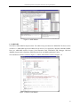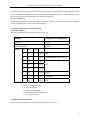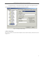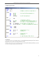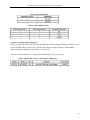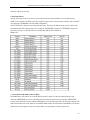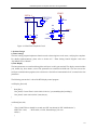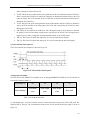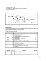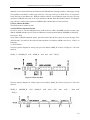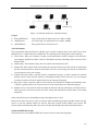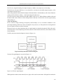
1
Embedded Systems Development and Labs; The English Edition
Embedded System Development and Application Course Series
Embedded System Development and Labs for
ARM
Edited, revised, and updated by Radu Muresan
Compound with Embest ARM Labs System
Compound with Multimedia Teaching Demo Modules
Embedded System Development and Application Course Series
Embedded Systems Development and Labs; The English Edition
To Readers
Embedded System Application Development and Labs Textbook is compounded with the Embest ARM
Development System that was developed by Embst Inc. at Shenzhen, China. Any reader who is interested in
using the Embest development tools for ARM can contact Embest Inc. The following is the Embest contact
information:
Room 509, Luohu Science&Technology Building,
#85 Taining Road, Shenzhen, Guangdong, China
ZIP: 518020
Tel: +86-755-25635656, 25635626
Fax: +86-755-25616057
Web: http://www.armkits.com or http://www.embedinfo.com
E-mail: [email protected]
Embedded System Development and Applications Textbook and Embedded System Application
Development and Labs Textbook are compounded with teaching demo modules separately. If you are
interested in any of these demo modules please contact Embest Inc.
2
Embedded Systems Development and Labs; The English Edition
An Introduction to This Book
This book is a Lab manual and is part of the “Embedded System Development and Application” course series.
This Lab manual is based on the Embest ARM Labs System development platform hardware, which uses an
ARM processor as its core. The Lab manual is a complete teaching and training tool for developing Embedded
Systems. The book contains 22 Labs that include: Labs for the embedded software development fundamentals;
Labs for basic interfaces; Labs for human-machine interface; Labs for communication and audio interfaces;
Labs for uC/OS-II embedded real-time operating system porting and application; etc. This book offers many
examples for the embedded system learners. The Labs form an embedded system teaching or training tool and
are introduced in a gradual manner from simple to complex applications that are close related to the engineering
world. This book is accompanied by a free CD that contains the Embest IDE Pro Education Version software
produced by Embest Inc.
This book can be used as a Lab teaching material for embedded and real-time embedded systems at
undergraduate or graduate level with majors in Commuter Science, Computer Engineering, Electrical
Engineering; or for professional engineers.
3
Embedded Systems Development and Labs; The English Edition
About the Editor of the English Version of the Embedded System Development and Labs
Radu Muresan is the editor of the English version of the “Embedded System Development and
Labs” book offered first in Chinese by Embest as an accompaniment book to their ARM
development platform. Radu Muresan has a PhD in Electrical and Computer Engineering from the
University of Waterloo Canada and is currently an assistant professor at the University of Guelph
Canada. He is currently teaching the Real-Time Systems Design course in the School of
Engineering using the “Embedded System Development and Labs” book and the Embest
development platform and tools.
4
Embedded Systems Development and Labs; The English Edition
FOREWORD
The Evolution of the Embedded Technology
The embedded systems based on 8-bits single-chip microprocessors have already being used in many fields.
Even today, most of the embedded applications are still belonging to the early stage of embedded system. A
general characteristic of these applications is that they include a MCU (micro-controller unit), sensors,
monitoring or testing devices, service systems, display devices, etc. Also, these applications have functions such
as testing, displaying, processing and automatic control of information. In some industrial control applications
such as automobile electronic systems and intelligent home electronic devices, these MCUs are interconnected
in a network through common buses such as CAN, RS-232, RS-485, etc. This kind of network has limited
applications. The related communication protocols are relatively simple and excluded to the Internet that is
being widely used. Today Internet has become a fundamental communication system that is serving the society
and also becomes an important way of exchanging information needed by the people. The embedded systems
can be integrated to the Internet, helping to transfer information world wide.
With the process of integration of embedded devices and Internet, complex high-end applications, mobile
phones, PDAs, routers, modems, etc will demand high performance from the embedded processors. Although
the embedded technologies that are based on the 8-bit single-chip computer still exist, these kinds of
technologies can’t meet the requirements of the evolution of the future embedded system technology due to its
limited functions. The market and technology competition consistently requires a higher function/price ratio.
On the other hand, the time development of an embedded system is also being required to be shorter and shorter.
From the early 70s when the embedded system concept has been introduced, the embedded systems have
evaluated rapidly and high performance and low power consumption systems have been developed. In the early
stages, many embedded system had no real time operation system (RTOS) support; those embedded system
were merely processing some functions such as simple controls that respond to the outside input through a
simple loop control algorithm, etc. With the evolution of technology, the system complexity increased and the
application fields of the embedded system expanded. Every time when some new functions were introduced, the
system software design needed to be completely changed. So, the lacking of real time operating system support
became an important issue. Due to the fact that running RTOS on an 8-bit single-chip processor has some
difficulties, the 32-bit microprocessor (as core of high performance embedded systems) became a common
trend of technology development.
From the early 90s, the way of embedded system design had gradually been changed from “Integrated Circuit”
level to “Integrated System” level. The “Integrated Circuit” is based on embedded microprocessors and DSPs.
The “Integrated System” is based on SoC (System on Chip) concept that was introduced at that time. Nowadays,
the embedded system has entered a design phase that is based on SoC and the SoC standardization is used more
and more. SoC provide complex hardware features for high performance embedded system. SoC also provides
the basic hardware support for real time embedded operating system. During 80s, some real time operating
systems emerged. The most common RTOS include VxWorks, Windows CE, Palm, ucLinux, pSOS, uC/OS etc.
However, the real application on these RTOS happened only in recent last few years.
There are two reasons for this development. One is the increased requirement of the complexity of embedded
5
Embedded Systems Development and Labs; The English Edition
software development in the last few years; another is the SoC. RTOS can be run in a dependable, effaceable
and affordable way. Most of the RTOS are expensive. As a result, some open sourced RTOS such as uc/OS-II,
ucLinux are being chosen by many users. These open sourced RTOS are also suitable as teaching tools. The
RTOS functionality and principles are relatively complex. Anyone who is interested in the RTOS research or
development, please refer to related books in the field.
Embedded systems based on embedded processor are characterized by small size, lightweight, low cost and
high performance. The largely used 32-bit microprocessors are ARM from ARM Ltd, Alpha from Compaq,
PA-RISE from HP, Power-PC from IBM, MIPS from MIPS Technologies Inc., SPARC from Sun etc.
ARM processors have merits of high performance, low power consumption, low cost, etc. ARM processors are
the most widely used microprocessors amongst the 32 bit and 64 bit microprocessors.
In the early 90s, the semiconductor industry formed a production chain that combined the design industry,
manufacture industry, packaging and testing industry. Some real semiconductor companies were greatly
developed and some fabless (chipless) companies also emerged. The Advanced RISC Machines (ARM), is the
most successful company based on the fabless chipless mode. ARM doesn’t produce or sale chips but provides
high performance IP cores that are being sold to authorized semiconductor companies.
Let’s look back to the development history of ARM technologies. At the time when ARM7 system architecture
(system architecture v3) was just been accepted and applied, the embedded microprocessor market was
overwhelmingly occupied by 8-bit and 16-bit microprocessors. However these microprocessors can’t meet the
requirements of developing high-end applications such as mobile phones, modems, etc. These high-end
products needed the 32-bit microprocessors processing power and higher programming code density than the
16-bit CISC processors. In order to meet these requirements, a T variety of ARM architecture was developed.
This T variety is called 16-bit Thumb Instruction Set. Thumb technology is one of the best characteristics of
ARM technology. The ARM7TDMIT (system architecture v4T) is the first microprocessor that supports Thumb
instruction set. ARM7TDMIT’s work mode can be switched to the Thumb working state. The 32-bit processor
can be run with 16-bit Thumb instruction set. So, thumb is a bridge between the 16-bit older system and the
32-bit new system. ARM architecture provided higher performance processor solutions to the users who were
looking for higher performance processors. These features greatly increased the embedded development as well
as ARM technology. The 16-bit microprocessors were not developed as people expected. The reason was
complicated. Maybe one of the reasons was that the 32-bit ARM processors provided higher performance and
lower price than the 16-bit processors and enabled the high-end embedded applications to jump to the new
32-bit generation.
Many semiconductor companies have accepted the ARM processor production development. There are more
than 100 IT companies that are currently using the ARM processors. Among them 19 of the 20 largest
semiconductor companies are developing chips based on the ARM architecture. These semiconductor
companies include TI, Philips, Intel etc. The excellent processor performance and the punctual marketing
enabled ARM to get tremendous resources. These resources greatly accelerated many kinds of system chips
developed for different applications. ARM has already established its lead position in the embedded
technologies and the ARM technologies are being widely used. ARM has gained great success in the field of
high performance embedded applications and the number one position in 32-bit embedded applications in the
world. In 2002, ARM processors occupied 79.5% of 32-bits and 64-bit microprocessor market in the world.
There were 20 billion ARM cores used by 2002. Nowadays, ARM processors are almost in everybody’s pocket
6
Embedded Systems Development and Labs; The English Edition
because almost all of the mobile phones, PDAs are developed based on ARM cores. As a result, in order to keep
up with the modern embedded technologies, people need to study the embedded development technologies that
are based on 32-bit ARM processors and also need to study its development environment and platform
technologies.
If integrated circuit and related technologies are the drivers of PC development that have increased the IT
technologies in the last twenty years, we could say that, besides the PC technologies, the portable, mobile and
Internet related embedded Internet information processing devices will be the main drivers that will enable a
Post-PC time becomes true in the next few decades. Currently the embedded Internet is merely limited to some
applications such as mobile business, intelligent electronic home devices, control and intelligent devices etc.
With the development of related technologies, embedded technology will be developed more and more at an
unimaginable speed with more complex applications. The area of embedded applications will be expanded and
the embedded systems and applications will be more valuable to the society.
Currently the Wintel (Microsoft an Intel federation established at early 90s) has dominated the computer
industry. With the development of information technology and network technology, the embedded technology
will make this monopoly not exist in the Post-PC time. Embedded System will be the main portion of non-PC
devices.
Current Status of Embedded System Tools for Teaching and Development
Human resource is the key of developing embedded system technology. Enhancing the embedded technology
teaching in the universities is to provide the embedded development human resources. On the other hand, the
existing engineering staffs in the companies are also needed to be trained by modern embedded technology.
The engineering staffs in companies welcome the embedded system training courses that are based on ARM. To
this point, establishing a new embedded system training system that is based on ARM is very necessary and
urgent. This kind of university training courses will resolve the problem of lacking technology human recourses
for developing embedded systems.
Although the ARM processors have higher performance and higher processing power than 8-bit single chip
computers such as 51 series microprocessors, the complexity and difficulty of developing embedded system
hardware and software based on ARM are greater.
The main purpose of establishing new tools based on ARM embedded technologies, is the need to enhance the
traditional embedded system training by adding complex embedded sample program modules, real time
operation system, etc to the text book to make the teaching closer to the real world of electrical and computer
engineering.
About the Course Series and Related Labs
In order to establish tools based on 32-bit ARM embedded technologies, the main requirement is
to develop the basic knowledge about ARM architectures. The “ARM System on Chip
Architecture” by Steve Furber together with the “ARM Architecture Reference Manual” by David
Seal can provide the necessary background.
7
Embedded Systems Development and Labs; The English Edition
The Course Series consists of the following basic textbooks:
Embedded System Development and Applications Textbook (Available in Chinese)
--Compound with multimedia demo modules
Major Contents: Basic concepts of embedded system application development, an overview of ARM
technology, ARM instruction set, the foundation of embedded program design based on ARM, development
samples based on ARM, open sourced real time operating system uC/OS-II and uCLinux, porting and
application software development. The readers can completely master the basic concepts and the design flow of
developing an embedded system, the embedded software development skills based on ARM, the basic concept
of porting and application development of embedded operating systems.
Embedded System Application Development and Labs Textbook
-- Compound with Embest ARM Labs System
--Compound with Multimedia Teaching Demo Modules
Major Contents: The embedded system application development Labs is based on the Embest ARM
development system. The Labs are coordinated with the course textbook Embedded System development and
Applications. The Labs include five parts: basic labs for embedded development, basic device interfacing labs,
complex human-machine interfacing labs, communication and voice interface labs, embedded RTOS
(Real-Time Operating Systems) porting and application development. These five parts have 22 Labs in total.
The labs increase in their difficulty as the book progresses through more material. The labs are very practical
and target real world applications. The readers can quickly master the skills that are needed to develop real
projects. The purpose of this book is to develop students’ creation ability, design ability, real world engineering
project development ability.
In order to coordinate with the course teaching and Lab teaching, we developed Multimedia Demo Modules for
the Embedded System Development and Applications and Embedded System Application Development and Labs
courses. As a start point, we will continually change or add new course textbooks, lab textbooks or multimedia
demo modules based on real practical teaching techniques and the evolution of related technologies.
This set of textbook combined with class teaching and lab teaching, provides a solution for students to master
embedded system development technologies based on ARM. The tools used in the ARM embedded application
development include the Integrated Development Environment (IDE), the Embedded Real-Time Operating
System, the evaluation board, the JTAG emulator, and other auxiliary tools. Generally, an Integrated
Development Environment (IDE) with its basic functions is the only nedded tool for embedded system
development. Others tools are optional.
The major IDEs used in the world include: SDT and ADS from ARM, Multi2000from GreenHill, Embest IDE
for ARM from Embest Inc, etc. The emulators used are Muti-ICE from ARM and ARM JTAG Emulater from
Embest Inc.
SDT and ADS is the IDE produced by ARM Ltd in its early state (discontinued). The S3C series chips from
SAMSUNG are the most widely used ARM based microprocessors. Embest Inc has developed the Embest
ARM Development board based on the S3C44B0 chip. This development board has memory, I/O, digital LCD
display, touch screen, keyboard, IIS, Ethernet interface, USB interface IIC interface, advanced extension
including IDE hard disk, CF card, flash disk etc. The Embest software and hardware tools are complete, reliable
and easy to use. These qualities are most needed in an university environment and made us use these tools for
8
Embedded Systems Development and Labs; The English Edition
our embedded based courses.
NOTE that other microprocessor and interfacing courses and textbooks can provide the basic
background for using the Embest development system.
The Prerequisites for Studying This Course Series
Before studying this course, students should have studied courses such as Microcomputer Interfacing, C
Language Programming, and have some basic knowledge of operating systems, computer architecture and
network protocols. The text book series have also presented background knowledge of basic networks protocol,
touch panel basics, keyboard interface programming basic etc.
9
Embedded Systems Development and Labs; The English Edition
Thanks (from Radu Muresan)
I am using this book to teach the “Real-Time Systems Design” course at the University of Guelph Canada. I
want to thank the Embest engineers {Liuchi, Zhang Guorui, Xu Guangfeng, Baidong} for their full support
during editing the English version of this book. They have provided detailed technical support and materials for
the assimilation of the existing labs and development of new labs. I also want to thank Oliver Zhihui Liu for
providing the first English draft of the Chinese version of the “Embedded Systems Development and Labs”
book. I have worked with his translation and generated the English version of the “Embedded Systems
Development and Labs”. In this version, I have updated the technical content of the labs based on the “ARM
Architecture Reference Manual”, I have verified all the labs and I have added a new real-time lab. Finally I want
to thank my master students Zhanrong Yang and Shukla Nupoor for their contributions to the testing of the labs.
Zhanrong Yang has work hard to help with the board setup and with providing support with the Chinese
documentation. Unfortunately, I was not able yet to edit other books based on the Embedded System
Development series. However, this lab manual can be combined with any microcomputer interfacing or
real-time system design courses offered in other universities.
Due to the fact that the translation draft was sort of word by word translation there are still English and technical
errors throughout the book. I have issued this version so the students can perform the required labs for my
Real-Time System Design course. I am still working on editing and updating the book and I hope to produce a
better version soon. Also, I am planning to produce an Embedded Real-Time system design text book that can
accompany this lab manual. However, I believe that this lab book is an excellent tool for teaching embedded
systems based on the ARM architecture. I have used other IDEs and I can say that the Embest engineers have
developed an excellent product. I want to congratulate the Embest engineers for putting together this product.
Radu Muresan, 2005
10
Embedded Systems Development and Labs; The English Edition
PREFACE
Theory teaching and Lab teaching are two important parts of the modern advanced education. Lab course is an
important part in the teaching process. This book is the Lab manual of the Embedded System Development
Course Series that provides teachers and students with complete embedded system training tools based on the
ARM architectures. In this Lab manual, we focus mainly on developing complete embedded applications using
the Embest development system. The applications provide the software and hardware details of the designs. We
integrated complex embedded system application sample modules, porting of embedded operating systems, etc.
Using this manual the students can learn not only the basics of the embedded system development, but also can
learn how to develop complex interface modules that apply to real world applications.
The following outlines the content of the chapters:
Chapter One: An overview of embedded system development, embedded system IDE, ARM embedded
development system, embedded study, etc.
Chapter Two: Embest embedded IDE for ARM, Embest ARM development system and Embest JTAG
emulator.
Chapter Three: Basic Labs of embedded software development based on ARM including: ARM basic
instruction set, Thumb instruction set, assembly programming, ARM processor mode switching, embedded C
programming, C and assembly language mix programming, overview of programming. (This chapter provides
the basic knowledge of embedded software development, basic programming skills, usage of IDE)
Chapter Four: Labs that target basic peripheral interfacing in embedded systems. The chapter includes
applications using memory, I/O interface, interrupts, serial communication, real-time clock and simple digital
LED interface.
(These Labs teach the student the basic principles of peripheral interfacing in embedded systems)
Chapter Five: Complex applications that introduce the human-machine interfacing. This chapter includes a
Lab using the LCD display, a Lab using the keyboard control, a Lab using the touch screen control.
(These Labs are more complex, difficult and closer to the real engineering applications. These labs require good
skills in using the Embest development system)
Chapter Six: Complex labs for developing applications using communication interfacing and IIS voice
interfacing. This chapter includes a Lab of IIC serial communication bus, a Lab of Ethernet communication and
a Lab of IIS voice bus interface communication.
(Chapters 4, 5, and 6 can prepare the students to develop applications using various interfaces and device
development that target real world applications.)
Chapter Seven: Introduces the uC/OS-II real-time operating system, porting and real-time application
development based on the Embest tools.
(Through the Labs of this chapter, the students will learn how to port uC/OS-II to the ARM processor and how
to build simple real-time applications based on the uC/OS-II kernel. They will learn the porting steps of the
uC/OS-II kernel to the ARM7 microprocessor, the boot flow of the uc/OS-II, the task management, the
inter-task communication, the synchronization and the memory management under uc/OS-II kernel.)
Appendix A and B: Instruction Quick Reference Table and Instruction Set Coding Table.
11
Embedded Systems Development and Labs; The English Edition
Appendix C: An introduction to Embest ARM products.
Appendix D: An introduction to the contents of the CD attached to this book.
The CD attached to this book is IDE Pro, a free educational version of the IDE software that Embest Inc
provides to the readers of this book. The readers can install this software and edit, compile and debug the sample
programs on a software target emulator. After this software is installed, the readers can find the basic Lab
sample software of Chapter 3 of this manual in the “\EmbestIDE\Examples\S3CEV40” directory. To run the rest
of the sample programs of the manual the readers need to purchase the full version of the Embest IDE, the
Embest development board and ICE emulator. The students should also study the embedded Lab development
system course that introduces computer interfacing, computer application software development, computer
operatimg systems, applied electronic technology, network communication, etc.
This lab manual can be used as a reference book for embedded system development based on ARM. There are
many real-time operating systems (RTOS) for embedded applications based on 32b-bit systems (RTOS such as
VxWorks, Windows CE, Palm, uClinux, uC/OS, etc). We have selected the uC/OS since this kernel is fully
documented and is an excellent tool for learning to develop real-time embedded applications.
This manual together with the Embest development system can be used in teaching undergraduate and graduate
courses in embedded systems design.
12
Embedded Systems Development and Labs; The English Edition
Chapter 1: An Overview of Embedded System Application Development 19
1.1 Embedded System Development and Applications .................................................................. 19
1.2 An Overview of Embedded Development Environment for ARM ........................................... 19
1.2.1 Cross Development Environment .................................................................................... 19
1.2.2 Software Emulator ........................................................................................................... 20
1.2.3 Evaluation Board ............................................................................................................. 20
1.2.4 Embedded Operation System........................................................................................... 20
1.3 An Overview of ARM Development system ............................................................................ 20
1.3.1 ARM SDT ........................................................................................................................ 20
1.3.2 ARM ADS........................................................................................................................ 21
1.3.3 Multi 2000........................................................................................................................ 22
1.3.4 Embeds IDE for ARM ..................................................................................................... 24
1.3.5 OPENice32-A900 Emulator ............................................................................................ 25
1.3.6 Multi-ICE Emulator ......................................................................................................... 25
1.4 How to Study Embedded System Application Development Based on ARM .......................... 26
Chapter 2: Embest ARM Lab Development system 27
2.1 An Overview of the Lab Development system ......................................................................... 27
2.1.1 The Embest IDE............................................................................................................... 28
2.1.2 Embest Emulator for ARM JTAG.................................................................................... 30
2.1.3 Flash Programmer............................................................................................................ 31
2.1.4 Embest S3CCEV40 Development Board......................................................................... 32
2.1.5 Connection Cables and Power Adapters .......................................................................... 33
2.2 The Installation of Lab Development system ........................................................................... 33
2.2.1 The Installation of Embest IDE........................................................................................ 33
2.2.2 The Installation of Flash Programmer.............................................................................. 36
2.2.3 The Interconnection of Software and Hardware Platforms.............................................. 37
2.3 Lab Development system Hardware Circuits ........................................................................... 37
2.3.1 An Overview of Lab Development Hardware ................................................................. 37
2.3.2 Hardware Reference for Software Design ....................................................................... 46
2.3.3 Bus Expansion ................................................................................................................. 50
2.4 The Usage of Embest IDE ........................................................................................................ 51
2.4.1 Embest IDE Main Window .............................................................................................. 51
2.4.2 Project Management ........................................................................................................ 51
2.4.3 Project Basic Settings ...................................................................................................... 54
2.4.4 Project Compiling and Linking........................................................................................ 68
2.4.5 Load Debugging............................................................................................................... 68
2.4.6 Flash Programmer............................................................................................................ 76
Chapter 3 Embedded System Development Basic Labs 78
3.1 ARM Assembly Instructions Lab 1........................................................................................... 78
3.1.1 Purpose............................................................................................................................. 78
13
Embedded Systems Development and Labs; The English Edition
3.1.2 Lab Equipment................................................................................................................. 78
3.1.3 Content of the Lab 1 ........................................................................................................ 78
3.1.4 Principles of the Lab 1 ..................................................................................................... 78
3.1.5 Lab 1 Operation Steps...................................................................................................... 80
3.1.6 Sample Programs of Lab 1............................................................................................... 84
3.1.7 Exercise............................................................................................................................ 87
3.2 ARM Assembly Instruction Lab 2 ............................................................................................ 87
3.2.1 Purpose............................................................................................................................. 87
3.2.2 Lab Equipment................................................................................................................. 87
3.2.3 Content of the Lab 2 ........................................................................................................ 88
3.2.4 Principles of the Lab 2 ..................................................................................................... 88
3.2.5 Lab Operation Steps......................................................................................................... 90
3.2.6 Sample Programs of Lab 2............................................................................................... 91
3.2.7 Exercises .......................................................................................................................... 92
3.3 Thumb Assembly Instruction Lab............................................................................................. 93
3.3.1 Purpose............................................................................................................................. 93
3.3.2 Lab Equipment................................................................................................................. 93
3.3.3 Content of the Lab ........................................................................................................... 93
3.3.4 Principles of the Lab ........................................................................................................ 93
3.3.5 Operation Steps of Lab 3 ................................................................................................. 95
3.3.6 Sample Programs ............................................................................................................. 95
3.3.7 Exercises .......................................................................................................................... 97
3.4 ARM Work Mode Labs............................................................................................................. 97
3.4.1 Purpose............................................................................................................................. 97
3.4.2 Lab Equipment................................................................................................................. 97
3.4.3 Content of the Lab ........................................................................................................... 97
3.4.4 Principles of the Lab ........................................................................................................ 97
3.4.5 Operation Steps of the Lab............................................................................................. 100
3.4.6 Sample Programs of the Lab.......................................................................................... 102
3.4.7 Exercises ........................................................................................................................ 104
3.5 C Language Program Lab 1 .................................................................................................... 104
3.5.1 Purpose........................................................................................................................... 104
3.5.2 Lab Equipment............................................................................................................... 104
3.5.3 Content of the Lab ......................................................................................................... 104
3.5.4 Principles of the Lab ...................................................................................................... 104
3.5.5 Operation Steps.............................................................................................................. 107
3.5.6 Sample Programs ........................................................................................................... 107
3.5.7 Exercises ........................................................................................................................ 108
3.6 C Language Program Lab 2 .................................................................................................... 108
3.6.1 Purpose........................................................................................................................... 108
3.6.2 Lab Equipment............................................................................................................... 109
14
Embedded Systems Development and Labs; The English Edition
3.6.3 Content of the Lab ......................................................................................................... 109
3.6.4 Principles of the Lab ...................................................................................................... 109
3.6.5 Operation Steps...............................................................................................................111
3.6.6 Sample Programs ........................................................................................................... 115
3.6.7 Exercises ........................................................................................................................ 118
3.7 Assembly and C Language Mutual Call ................................................................................. 118
3.6.1 Purpose........................................................................................................................... 118
3.6.2 Lab Equipment............................................................................................................... 118
3.6.3 Content of the Lab ......................................................................................................... 118
3.6.4 Principles of the Lab ...................................................................................................... 118
3.7.5 Operation Steps.............................................................................................................. 120
3.7.6 Sample Programs ........................................................................................................... 121
3.7.7 Exercises ........................................................................................................................ 124
3.8 Sum Up Programming ............................................................................................................ 124
3.8.1 Purpose........................................................................................................................... 124
3.8.2 Lab Equipment............................................................................................................... 124
3.8.3 Content of the Lab ......................................................................................................... 124
3.8.4 Principles of the Lab ...................................................................................................... 124
3.8.5 Operation Steps.............................................................................................................. 126
3.8.6 Sample Programs ........................................................................................................... 129
3.8.7 Exercises ........................................................................................................................ 132
Chapter 4 Basic Interface Labs 133
4.1 Memory Lab ........................................................................................................................... 133
4.4.1 Purpose........................................................................................................................... 133
4.4.2 Lab Equipment............................................................................................................... 133
4.1.3 Content of the Lab ......................................................................................................... 133
4.1.4 Principles of the Lab ...................................................................................................... 133
4.1.5 Operation Steps.............................................................................................................. 140
4.4.6 Sample Programs ........................................................................................................... 141
4.1.7 Exercises ........................................................................................................................ 145
4.2 I/O Interface Lab..................................................................................................................... 145
4.2.1 Purpose........................................................................................................................... 145
4.2.2 Lab Equipment............................................................................................................... 145
4.2.3 Content of the Lab ......................................................................................................... 145
4.2.4 Principles of the Lab ...................................................................................................... 145
4.2.5 Operation Steps.............................................................................................................. 148
4.2.6 Sample Programs ........................................................................................................... 149
4.2.7 Exercises ........................................................................................................................ 153
4.3 Interrupt Lab ........................................................................................................................... 153
4.3.1 Purpose........................................................................................................................... 153
4.3.2 Lab Equipment............................................................................................................... 153
15
Embedded Systems Development and Labs; The English Edition
4.3.3 Content of the Lab ......................................................................................................... 153
4.3.4 Principles of the Lab ...................................................................................................... 154
4.3.5 Operation Steps.............................................................................................................. 161
4.3.7 Exercises ........................................................................................................................ 165
4.4 Serial Port Communication Lab.............................................................................................. 165
4.4.1 Purpose........................................................................................................................... 165
4.4.2 Lab Equipment............................................................................................................... 165
4.4.3 Content of the Lab ......................................................................................................... 165
4.4.4 Principles of the Lab ...................................................................................................... 165
4.4.5 Operation Steps.............................................................................................................. 171
4.5.6 Sample Programs ........................................................................................................... 171
Exercises ................................................................................................................................. 176
4.5 Real-Time Timer Lab.............................................................................................................. 176
4.5.1 Purpose........................................................................................................................... 176
4.5.2 Lab Equipment............................................................................................................... 176
4.5.3 Content of the Lab ......................................................................................................... 176
4.5.4 Principles of the Lab ...................................................................................................... 176
4.5.5 Lab Design..................................................................................................................... 178
4.5.6 Operation Steps.............................................................................................................. 180
4.5.7 Sample Programs ........................................................................................................... 180
4.5.8 Exercises ........................................................................................................................ 185
4.6 8-SEG LED Display Lab ........................................................................................................ 185
4.6.1 Purpose........................................................................................................................... 185
4.6.2 Lab Equipment............................................................................................................... 185
4.6.3 Content of the Lab ......................................................................................................... 185
4.6.4 Principles of the Lab ...................................................................................................... 185
4.6.5 Operation Steps.............................................................................................................. 188
4.6.6 Sample Programs ........................................................................................................... 188
4.6.7 Exercises ........................................................................................................................ 189
Chapter 5 Human Interface Labs
190
5.1 LCD Display Lab.................................................................................................................... 190
5.1.1 Purpose........................................................................................................................... 190
5.1.2 Lab Equipment............................................................................................................... 190
5.1.3 Content of the Lab ......................................................................................................... 190
5.1.4 Principles of the Lab ...................................................................................................... 190
5.1.5 Lab Design..................................................................................................................... 199
5.1.6 Operation Steps.............................................................................................................. 202
5.1.7 Sample Programs ........................................................................................................... 203
5.1.8 Exercises ........................................................................................................................ 209
5.2 4 x 4 Keyboard Control Lab ................................................................................................... 209
5.2.1 Purpose........................................................................................................................... 209
16
Embedded Systems Development and Labs; The English Edition
5.2.2 Lab Equipment............................................................................................................... 209
5.2.3 Content of the Lab ......................................................................................................... 209
5.2.4 Principles of the Lab ...................................................................................................... 209
5.2.5 Lab Design..................................................................................................................... 210
5.2.6 Operation Steps.............................................................................................................. 214
5.2.7 Sample Programs ........................................................................................................... 214
5.2.8 Exercises ........................................................................................................................ 218
5.3 Touch Panel Control Lab ........................................................................................................ 218
5.2.1 Purpose........................................................................................................................... 218
5.2.2 Lab Equipment............................................................................................................... 218
5.2.3 Content of the Lab ......................................................................................................... 218
5.2.4 Principles of the Lab ...................................................................................................... 218
5.3.5 Lab Design..................................................................................................................... 221
5.3.6 Operation Steps.............................................................................................................. 223
5.3.7 Sample Programs ........................................................................................................... 224
5.3.8 Exercises ........................................................................................................................ 229
Chapter 6 Communication and Voice Interface Labs
230
6.1 IIC Serial Communication Lab ............................................................................................... 230
6.1.1 Purpose........................................................................................................................... 230
6.1.2 Lab Equipment............................................................................................................... 230
6.1.3 Content of the Lab ......................................................................................................... 230
6.1.4 Principles of the Lab ...................................................................................................... 230
6.1.5 Lab Design..................................................................................................................... 237
6.1.6 Operation Steps.............................................................................................................. 238
6.1.7 Sample Programs ........................................................................................................... 239
6.1.8 Exercises ........................................................................................................................ 239
6.2 Ethernet Communication Lab ................................................................................................. 242
6.2.1 Purpose........................................................................................................................... 242
6.2.2 Lab Equipment............................................................................................................... 242
6.2.3 Content of the Lab ......................................................................................................... 242
6.2.4 Principles of the Lab ...................................................................................................... 242
6.2.5 Operation Steps.............................................................................................................. 256
Sample Programs .................................................................................................................... 256
Exercises ................................................................................................................................. 259
6.3 IIS Voice Interface Lab ........................................................................................................... 259
6.3.1 Purpose........................................................................................................................... 259
6.3.2 Lab Equipment............................................................................................................... 259
6.3.3 Content of the Lab ......................................................................................................... 259
6.3.4 Principles of the Lab ...................................................................................................... 259
6.3.5 Sample Programs ........................................................................................................... 263
6.3.6 Exercises ........................................................................................................................ 268
17
Embedded Systems Development and Labs; The English Edition
Chapter7 Real Time Operation System Labs 269
7.1 uC/OS Immigration Lab ......................................................................................................... 269
6.3.1 Purpose........................................................................................................................... 269
7.1.2 Lab Equipment............................................................................................................... 269
7.1.3 Content of the Lab ......................................................................................................... 269
7.1.4 Principles of the Lab ...................................................................................................... 269
7.1.5 Sample Programs ........................................................................................................... 272
Exercises ................................................................................................................................. 275
7.2 uC/OS Application Lab........................................................................................................... 275
7.2.1 Purpose........................................................................................................................... 275
7.1.2 Lab Equipment............................................................................................................... 275
7.1.3 Content of the Lab ......................................................................................................... 275
7.1.4 Principles of the Lab ...................................................................................................... 275
7.2.5 Sample Programs ........................................................................................................... 277
7.2.6 Exercises ........................................................................................................................ 279
Appendix A ARM Instruction, ARM Addressing and Thumb Instruction Quick Reference
287
Appendix B ARM and Thumb Instruction Code
288
Appendix C Embest ARM Related Products 289
Appendix D Content of CD-ROM
290
Reference Documentations 291
18
Embedded Systems Development and Labs; The English Edition
Chapter 1: An Overview of Embedded System Application
Development
1.1 Embedded System Development and Applications
Embedded system based on embedded microprocessor is a new technology direction in IT technology.
ARM series processors are products from Advanced RISC Machine. The current ARM core includes
ARM7TDMI, ARM720T, ARM9TDMI, ARM920T, ARM940T, ARM946T, ARM966T and Xscale, etc.
Recently ARM Ltd. renounced to 4 ARM11 microprocessors (ARM1156T2-S, ARM1156T2F-S, ARM1176JZ
and ARM11JZF-S). ARM chips are supported by many real time operating systems providers such as
WindowsCE, uCLinux, VxWorks, Nucleus, EPOC, uc/OS, BeOS, Palm and QNX, etc.
1.2 An Overview of Embedded Development Environment for ARM
1.2.1 Cross Development Environment
Cross development means editing and compiling software on a general-purpose computer, and then
downloading the software to the embedded device and debugging it on both, host and target. The
general-purpose computer is called host. The embedded device is called target. Cross Development
Environment consists of cross development software running on the host PC and the debug channel from host to
target. There are three types of debug channels from host to target:
1. The JTAG Based ICD
JTAG based ICD (In-Circuit Debugger) is also called JTAG Emulator. The JTAG Emulator connects to the
target through the JTAG interface of the ARM processor and connects to the host through the serial port, the
network port, or the USB port. JTAG Emulator has the following functions:
● Read/write CPU registers, visit and control ARM processor core.
● Read/write memory.
● Visit ASIC system.
● Visit I/O system.
● Single step execute program and real time execute program.
● Set break points.
JTAG Emulator is the most widely used debug method.
2. Angel Debugging Software
Angel debug monitor software is a group of software programs running at the target board. It receives debug
commands from host to set break points, single step execute programs, read/write memory, etc. Angel software
is cheap and it doesn’t need any other hardware debugging emulators. The inconvenient of this software is that
it can be used only after the hardware is in a stable state.
3. The In Circuit Emulator (ICE) is a CPU emulation device.
The ICE can completely emulate a target CPU such as the ARM processor and provides deeper debug functions.
19
Embedded Systems Development and Labs; The English Edition
Serial port, network port and USB port are also the communication channels of ICE. ICE can emulate high
speed ARM processor. ICE is expensive and normally used in hardware development. It is seldom used in
software development.
1.2.2 Software Emulator
Software Emulator can partly emulates the target hardware. It is normally an instruction set emulator. Software
emulator can only be used as a primary debug tool because its function is limited and can’t completely emulate
the real hardware.
1.2.3 Evaluation Board
The evaluation board is also called a development board. It is useful for the developers. Experienced engineers
can also make their own development board. A good development board has complete documentation, hardware
and software implementations, schematic, sample programs, source code, etc for development references.
1.2.4 Embedded Operation System
Embedded real time operation system (RTOS) provides memory management, task management and resource
management, etc. RTOS can save a lot of troubles in complicated applications. But if the application is not
complicated, embedded systems can run without real time operation systems.
1.3 An Overview of ARM Development system
1.3.1 ARM SDT
ARM SDK is called ARM Software Development Kit. It is made by ARM Ltd. The latest version is 2.5.2. The
highest ARM processors it can support are ARM9 series. ARM Ltd will not continue the ARM SDK in the
future. The user interface of ARN SDK is shown in Figure 1-1 and Figure 1-2.
Figure 1-1 ARM Project Manager
20
Embedded Systems Development and Labs; The English Edition
Figure 1-2 ADW Window
1.3.2 ARM ADS
The ADS is called ARM Development Suite. The ADS is being used instead of ARM SDK. The latest version
of ADS is 1.2. ARM ADS supports all ARM series processors. It is supported by Windows 2000/Me, RedHat
Linux, etc. ARM ADS consists of 6 parts: Code Generation Tools, CodeWarrior IDE, Debugger (ADS and
ARMSD), Instruction Set Simulators, ARM Firmware Suite and ARM Applications Library.
The CodeWarrior interface is shown in Figure 1-3 and the ADS interface is shown in Figure 1-4.
Figure 1-3 Source Code Window
21
Embedded Systems Development and Labs; The English Edition
Figure 1-4 ADS Windows
1.3.3 Multi 2000
Multi 2000 is developed by Green Hills (www.ghs.com). Multi 2000 supports C/C++, Embedded C++, Ada95
and Fortran, etc programming languages. It can be run on Windows and Unix and supports remote debugging.
Multi 2000 supports various 16-bit, 32-bit and 64-bit CPUs and DSPs such as PowerPC, ARM, MIPS, X86,
Sparc, Tricore and SH-DSP etc. Multi2000 also supports multiple CPU debugging. Multi 2000 consists of
Project Builder (Figure 1-6), Source-Level Debugger (Figure 1-7), Event Analyzer (Figure 1-8), Performance
Profiler (Figure 1-9), Run-Time Error Checking, Graphic Browser (Figure 1-10), Text Editor and Version
Control System.
Figure 1-5 Multi 2000
22
Embedded Systems Development and Labs; The English Edition
Figure 1-6 Project Builder
Figure 1-7 Source-Level Debugger
Figure 1-8 Event Analyzer
23
Embedded Systems Development and Labs; The English Edition
Figure 1-9 Performance Profiler
Figure 1-10 Graphic Browser
1.3.4 Embest IDE for ARM
Embest IDE is called Embest Integrated Development Environment developed by Embest Info&Tech Co.,LTD
(www.embedinfo.com). Embest IDE is a highly integrated graphic development environment that includes an
editor, compiler, debugger, project manager, flash programmer, etc. Embest IDE currently supports all the
processors based on ARM7 and ARM9. Also, the software can be upgraded to support the new ARM cores. The
Embest IDE interface is shown is Figure 1-11.
24
Embedded Systems Development and Labs; The English Edition
Figure 1-11 Embest IDE for ARM Windows
1.3.5 OPENice32-A900 Emulator
OpenNice32-A900 emulator is produced by AIJI (www.aijisystem.com). OPENNice32-A900 is a JTAG
emulator and supports ARM7/ARM9/ARM10 and Intel Xscale processor series.
The OPENNice32-A900 has the following features:
● Supports multiple CPUs or multiple CPU boards.
● Supports assembly and C language debugging.
● Provides On_board Flash programming tool.
● Provides memory controller configuration GUI.
● Software can be upgraded to support new ARM cores.
1.3.6 Multi-ICE Emulator
Multi-ICE is a JTAG emulator developed by ARM Ltd. The latest version is 2.1. Multi-ICE supports external
power supply. This is important for debugging devices such as mobile phones, battery power supply devices,
etc.
The following are the advantages of the Multi-ICE emulation:
● Rapid download and single step program execution.
● User controlled input/output at bit level.
● Programmable JTAG bit transfer rates.
25
Embedded Systems Development and Labs; The English Edition
●
●
●
Open interface support for non-ARM cores and DSPs.
Multiple debuggers can be connected to the network.
Target board power supply or external power supply.
1.4 How to Study Embedded System Application Development Based on ARM
First, the readers need to study the basic knowledge related to the microprocessor organization and interfacing
(Flash/SRAM/SDRAM/Catch, UART, Timer, GPIO, Watchdog, USB, IIC, etc), understand one CPU
architecture, understand operating system basics (interrupt, priority, inter-task communication and
synchronization, etc). For programming, readers need to master C, C++ and assembly language programming
(at least C language programming), understand microprocessor architecture, instruction set, programming
modes, application development, etc. Secondly, the student of embedded system development needs a good
development platform. Also, good development system with basic examples and typical real life application are
essential.
26
Embedded Systems Development and Labs; The English Edition
Chapter 2: Embest ARM Lab Development system
2.1 An Overview of the Lab Development system
The Embest ARM Lab development system includes:
● Embest IDE for ARM 2003
● Embest Emulator for ARM JTAG
● Flash Programmer
● Embest S3CEV40 Development Board
● Connection Cables, Power Adapters and Lab Guide
● Two CDs:
-- An Embest IDE for ARM Software Installation CD
-- A Compound Lab Development system CD
Embest IDE software and Flash Programmer software are on the Embest IDE for ARM Software Installation
CD. The content of the compounded CD includes: Embest S3CEV40 Evaluation Board Manual, Schematics of
Evaluation Board, Boot Program, Function Module Test Programs, uC/OS-II Real Time Operation System, etc.
This CD also has all the source code of this Lab course. (PLEASE NOTE that some of the resources are in
Chinese and the ones that are in English need to be corrected)
In order to run the sample programs of this Lab course, please copy the content of the CD in the following
directory: C:\Embest\Examples\Samsung\S3CEV40. “C:” is the default hard drive. Users can select different
hard drives during the installation process. In all the Labs of this book, the directory
“C:\Embest\Examples\Samsung\S3CEV40” is called “sample program directory”.
Attached to this book is the latest version of the IDE Education Version. The installation process of this software
is exactly the same as the installation process of normal version Embest IDE for ARM 2003 that provided in the
full Embest IDE version. During the installation process of the IDE Education Version, the source code of
Chapter 3 is automatically copied in the directory C:\Embest\Examples\Samsung\S3CEV40. A basic model of
Embest ARM development system is shown in Figure 2-1.
27
Embedded Systems Development and Labs; The English Edition
Figure 2-1 Model diagram of the Labs
2.1.1 The Embest IDE
1. An Overview of Embest IDE
Embest is a new generation of integrated development environment that is being used in embedded software
development. It provides high efficiency and clear graphic interface for embedded software development. It
provides a set of development and debugging tools that include: editor, compiler, linker, project manager, etc.
The style of the Embest IDE is similar to that of the Microsoft Visual Studio. It is a set of visual development
system for embedded software development. In this IDE, the user can conveniently create or open projects;
create or open files; compile, link, run or debug various kinds of embedded programs. The Embest IDE
interface is shown in Figure2-2
28
Embedded Systems Development and Labs; The English Edition
Figure 2-2 Interface of Embest IDE
2. Features of Embest IDE
Embest IDE can be run under various operating systems such as Windows 98, 2000, NT, XP etc. It mainly
supports ARM processors (currently ARM7 and ARM 9 series). The first version of Embest IDE for ARM was
finished in 2001. The latest version is the 2003 Embest IDE for ARM.
The following are the important features of Embest IDE for ARM:
● Supported programming languages: C and assembly.
● Friendly and convenient interface: Microsoft Visual Studio user like interfaces.
● Project Manager: Graphic project management tools that organize and manage the source code files. It
provides Windows for compiling, linking, library settings. Multiple software projects or multiple library
projects can be managed in the same work zone.
● Source Code Editor: Standard text editor that supports color display for key words, syntax key word etc.
The IDE also provides find string engine for quick search.
● Compile Tool: The GCC from GNU has been optimized and strictly tested in Win32 environment. The IDE
provides a graphic compiler setting interface. The user can use simple, fast, and direct settings for a project
compilation. The output of the compilation information is clear and organized for the users to quickly locate
the syntax errors in their source code.
● Debugger: Source code level debugging. The debugger provides two debugging ways that are graphic
interface debugging and command line debugging. The debugger is capable of setting break points, single
step source code execution, exception processing, peer or modify memory, register values and variables,
29
Embedded Systems Development and Labs; The English Edition
peer the function stack, disassembly code, etc.
● Debug Device: Embest JTAG Emulator. One of its ends is DB25 interface that connect to the parallel port
of a PC, another end is an IDC plug that connects to the JTAG interface of the target board. Users can use
Embest IDE and Embest JTAG Emulator together for software development. Embest IDE also supports
universal JTAG cables connectivity.
● Off-line debugging: Embest IDE for ARM provides an ARM instruction emulator. Users can debug ARM
application software on PC without the target hardware connected.
● A rich set of sample programs: Provides sample programs for debugging and usage descriptions for ARM
processors from many companies such as Atmel, Samsung, Cirrus Logic, OKI, etc.
● On-line Help: English and Chinese version on-line helps files.
When developing embedded software, the first step is the design, the second step is the programming, and the
third step is the debugging. A few thousand lines program could have no warnings in the compilation, but will
not meet the requirements when executed in hardware. Or, the program will cause system collapse and no
startup. Errors such as run time random problems and system collapse are hard to solve. The Embest IDE
debugger and debug devices provide Windows debugging environment for program loading, execution, run
time control and monitoring of various debug information.
The Embest debugging functions include:
● Break points: Break point setting, break point shielding, break point cancellation, conditional break point,
break point listing.
● Single step execution of programs.
● Variable monitoring functions: Variable value display can be changed while the program is executing,
variables can also be modified at run time.
● Memory content display and modification, memory content display format setting.
● Stack display.
● Graphic interface debugging and command line debugging.
● Multiple display mode for the same source code: the source code can be displayed as source, assembly or
mixed source/assembly.
● Provides MS Visual Studio like debug menu: Go, Stop, Step into, Step over, Step out, Run to Cursor, etc.
● Program uploads and downloads.
2.1.2 Embest Emulator for ARM JTAG
JTAG emulator is also called JTAG debugger. The JTAG emulator communicates with the ARM core through a
JTAG loop interface. This debugging method doesn’t need to use the main resources on the chip. It doesn’t need
the target memory and it doesn’t occupy any peripheral ports of the target system.
Because the target programs are executed by the target board, the emulation is closer to the hardware. Some
interfacing problems such as high frequency restriction, AC and DA parameter matching problems, length of
wires, etc have been minimized. The combination of IDE and JTAG Emulator is the most commonly used way
of debugging. The Embest Emulator for ARM is shown in Figure 2-3.
30
Embedded Systems Development and Labs; The English Edition
Figure 2-3: Embest Emulator for ARM JTAG
2.1.3 Flash Programmer
After the programming is finished, the user needs to download the binary code into the flash memory for run
time testing. Embest Inc. provides a Flash Programmer that allows the user to directly write the flash of the
development board. (The Flash Programmer needs to work together with the Embest Emulator for ARM JTAG.)
The windows interface is shown in Figure 2-4.
Figure 2-4 Flash Programmer Windows
The following are the features of the Flash Programmer:
● Supports all ARM7 and ARM 9 microprocessors: ATMEL AT91, INTEL 28 Series, SST 29/39/49 series.
● Flash empty memory space checking, memory erasing; memory programming, file verification, protection
and uploading.
31
Embedded Systems Development and Labs; The English Edition
●
●
●
●
Specific memory sector operations without changing other memory sectors.
8-bit, 16-bit and 32-bit read/write width.
Support for 1 to 4 flash chips programming, program files doesn’t need to be split
Support for Windows 98, 2000, NT and XP operating systems.
2.1.4 Embest S3CCEV40 Development Board
Embest S3CEV40 is the hardware platform of the Lab development system. It is an ARM development board
developed by Embest Inc. with full functions. This board provides various resources and is based on the
Samsung S3C44B0X microprocessor (ARM7TDMI). The hardware consists mostly of commonly used devices
to develop an embedded system. These devices are serial port, Ethernet port, voice output port, LCD and TSP
touch screen, 4x4 small keyboard, Solid-State Hard Disc, Flash, SDRAM, etc. After this course, users could not
only finish the examples that are provided by the Lab system, but also could build their own target systems. The
hardware platform is shown in Figure 2-5.
Figure 2-5 Lab System Hardware Platform
The following are the basic features of the S3CEV40 development board:
● Power supply: 5V power supply or USB power supply via PC, LED power status display, 500mA fuse.
● 1M x 16 bit Flash
● 4 x 1M x 16 bit SDRAM
● 4Kbit IIC bus serial EEPROM
● 2 serial ports: one is a simple interface port, another is a full interface port that can be connected to the
RS232 MODEM
● Reset switch
● Two interrupt buttons, two LEDs
● IDE hard disk interface
● LCD and TSP touch screen interfaces
32
Embedded Systems Development and Labs; The English Edition
●
●
●
●
●
●
●
●
●
●
20 pin JTAG interface
USB connector
4x4 keyboard interface
Four 2 x 20 extended CPU interfaces
10 Mb/s Ethernet interface
8 segment LED
Microphone input port
IIS voice signal output port that can be connected to a two channel speaker
16M x 8 bit Solid-State Hard Disc
320x240 LCD panel with a touch screen panel
2.1.5 Connection Cables and Power Adapters
Besides the above components, the Lab system also provides cables for interconnections including a network
cable, a USB cable, a serial cable, a parallel cable, 2 JTAG cable (20 pins and 16 pins). The lab system also
provides a 5V power adapter for the Embest S3CEV40 board.
2.2 The Installation of Lab Development system
The Embest ARM Lab system consists of Embest IDE, Flash programmer, Embest Emulator for ARM JTAG,
Embest S3CEV40 development board, various cables and a power adapter. The software platform is composed
of the Embest IDE and the Flash programmer. The rest are part of the hardware platform. This section is mainly
about how to install and setup the software platform. The software platform installation includes:
● Embest IDE installation
● Embest Flash Programmer installation
2.2.1 The Installation of Embest IDE
Insert the “Embest IDE for ARM Software Installation CD” into your CD-ROM, an the installation process is
automatically started. This is shown in Figure 2-6. Click “ENGLISH”, and a new interface will shown (See
Figure 2-7).
33
Embedded Systems Development and Labs; The English Edition
Figure 2-6 Embest IDE Installation Interface
Figure 2-7 Installation Software Selection Interface
Select “Embest IDE for ARM 2003”, click on the name of the software and run the installation. This is shown in
Figure 2-8 and Figure 2-9.
34
Embedded Systems Development and Labs; The English Edition
Figure 2-8 Installation Program Boot Interface
Figure 2-9 Select Type of Setup
After the installation, the system will prompt you to reboot the computer. After the computer is rebooted, an
icon of Embest IDE will be displayed on the desktop. Double click on this icon to run Embest IDE. When the
Embest IDE is first time started, the software will prompts to a registration dialog box as shown in Figure 2-10.
35
Embedded Systems Development and Labs; The English Edition
Figure 2-10 Registration Information Dialog
After you fill correctly the user information, click on the “Generate Key.dat” button. The software will generate
a key.dat file in the License subdirectory. Send the key.dat file to [email protected] via email. The user
will receive a License.dat file in 24 hours. Copy the License.dat file to the License subdirectory. Restart the IDE,
and the Embest IDE will work properly.
2.2.2 The Installation of Flash Programmer
Refer to Figure 2-7, select “Embest Online Flash Programmer” and run the installation. An interface as shown
in Figure 2-11 will be started.
Figure 2-11 Flash Programmer Installation Interface
Follow the installation steps and finish the installation.
36
Embedded Systems Development and Labs; The English Edition
2.2.3 The Interconnection of Software and Hardware Platforms
As shown in Figure 2-12, the Emulator is connected to the PC via a parallel cable and is connected to the target
board via a 20-pin JTAG cable.
Figure 2-12 Lab Platform Interconnection Diagram
2.3 Lab Development System Hardware Circuits
2.3.1 An Overview of the Lab Development system Hardware
1. Embest ARM Lab Development system
The Embest ARM Development system block diagram is shown at Figure 2-13.
37
Embedded Systems Development and Labs; The English Edition
Figure 2-13 Embest S3CEV40 Function Block Diagram
2. Memory System
The Lab system has one 1Mx16 Flash chip (SST39VF160) and a 4Mx16 SDRAM chip (HY57V65160B). The
flash chip interconnection diagram is shown in Figure 2-14. The pin nGCS0 of 44B0X microprocessor chip is
connected to the pin nCE of SST39VF160 flash chip. Because the flash chip is 16 bit, the address bus A1-A20
of 44B0X CPU is connected to the A0-A19 of the SST39VF160 flash chip. The memory space address of the
Flash is 0x000000-0x00200000.
The SDRAM circuit interconnection diagram is shown at Figure 2-15. The SDRAM has four banks. Each bank
has 1Mx16 bit. The address of the bank is decided by pin BA1 and BA0: 00 selects Bank0, 01 selects bank1, 10
selects Bank2, and 11 selects Bank3. The row address pulse RAS and the column address pulse CAS are used in
addressing each banks. The Lab system provides jumpers for the users to upgrade the capability of SDRAM up
to 4x2M x16 bit. The upgrade method is done by connecting the pin BA0, BA1 of SDRAM chip to the pins A21,
A22, A23 of CPU chip. The SDRAM will be the chip selected by a specified chip selection signal nSCS0 of the
CPU. The SDRAM memory space is 0x0C000000-0x0C8000000.
38
Embedded Systems Development and Labs; The English Edition
A(20..1)
A(19..0)
D(15..0)
DQ(15..0)
nGCS0
nCE
nOE
nOE
nWE
nWE
44B0X
SST39VF160
FLASH
Figure 2-14 Flash Interconnection Circuit Diagram
A(12..1)
A(11..0)
D(15..0)
D(15..0)
nSRAS
nSCAS
nSCS0
nOE
DQM0
DQM1
nRAS
nCAS
nCS
nWE
LDQM
UDQM
A21
A22
A23
44B0X
R1
R2
UNLOAD
R3
R4
BA0
BA1
SDRAM
UNLOAD
Figure 2-15 SDRAM Interconnection Circuit Diagram
3. IIC EEPROM Interface
The Lab system provides a 4Kb EEPROM chip (AT24C04) that supports the IIC bus. The IIC is a two direction,
two wires serial simple bus that is used for internal IC control. The data transfer speed is 100kb/s in the standard
mode. The data transfer speed can be as high as 400kb/s in the high-speed mode.
4. Serial Interface
The serial interface of the circuit is shown in Figure 2-16. The Lab system provides two serial ports (DB9). One
is the main port UART1 that is used to communicate with the PC or the MODEM. Because the S3C44B0X
doesn’t provides the I/O modem interface signals DCD, DTR, DSR, RIC, the MCU general purpose I/O must be
used. The other serial interface is UART0 that has two wires RxD and TxD for simple data
receiving/transmitting. The UART1 port uses MAX3243E for voltage conversion. The UART0 uses
MAX3221E for voltage conversion.
39
Embedded Systems Development and Labs; The English Edition
44B0X
GPE1
MAX3221E
TIN
TOUT
DB9 UART0
2
ROUT
RIN
GPE2
3
MAX3243E
T1IN
T1OUT
T2IN
T2OUT
T3IN
T3OUT
R1OUT
R1IN
R2OUT
R2IN
R3OUT
R3IN
R4OUT
R4IN
R5OUT
R5IN
PC12
PC10
PC15
PC13
PC11
PC8
PC9
PC14
DB9 UART1
Figure 2-16 Serial Port Circuit Diagram
5. USB Circuit Module
The USB module circuit is shown in Figure 2-17. The IC chip is USBN9603. A company named NS makes this
USB controller. The USB controller supports the USB1.0 and USB1.1 communication protocols and has a
parallel bus. It has three work modes that are Non-Multiplexing Parallel Interface Mode, Multiplexed Parallel
Interface Mode, and MICROWIRE Interface Mode. The mode selection is decided by the pins MODE1 and
MODE2. If the MODE1, MODE2 are connected to ground, the work mode is defined as Non-Multiplexing
Parallel Interface Mode. In this mode, the pin DACK should be connected to high because DMA is not used.
The MCP will select the USB controller using chip selection signal CS1 that is generated by the decoder. The
USBN9603 sends the interrupt request to the MCU through the pin EXINT0.
D(7..0)
D(7..0)
A1
A0
nOE
RE
nWE
WE
44B0X
D+
USBN9603
nRESET
RESET XOUT
EXINT0
INTR
CS1
2
USBPORT
3
D-
C1
X3
24MHz
R1
C2
CS
XIN
Figure 2-17 USB Circuit Diagram
6. Ethernet Circuit Module
The Ethernet circuit module is shown in Figure 2-17. The Embest Development system uses REALTEK’s
40
Embedded Systems Development and Labs; The English Edition
RTL8019AS a full duplex Ethernet controller that can be hot swapped. The followings are the features of this
Ethernet controller chip:
● Meet the standard of Ethernet II and IEEE802.3.
● Full duplexes send and receive at 10Mb/s.
● Internal 16KB SRAM for send/receive buffering. This buffer can reduce the speed requirements of the main
CPU.
● Support 8/16-bit data bus, 8 interrupt lines, and 16 I/O base address selections.
● Support UTP, AVI and BNC auto detection, support auto polar modification for the 10BaseT network
architecture.
● Four LED programmable output
● 100 pin PQFP package that minimized the size of the PCB board.
D(15..0)
SD(15..0)
A(12..8)
EXINT3
nOE
nWE
nRESET
SA(4..0) TPIN+
TPININT0
LD
IORB
HD
IOWB
RSTRV
A20
A19
A18
nGCS1
44BOX
A2
A1 Y7 CS7
A0
S3
74LV138
4
6
3
1
7
9
10
12
FB2022
3
6
2
1
RJ45
AEN
RTL8019AS
Figure 2-18 Ethernet Circuit Diagram
RTL8019AS has three work modes. If 93C46 is not used in the embedded application, the cost could be reduced
and the wiring. Thus the jumper work mode is normally used. The I/O address of the network card is decided by
IOS3, IOS2, IOS1 and IOS0. There are two RAMs that are integrated in the RTL8019. One is a 16KB from
0x4000 to 0x7FFF and another is a 32 bit from 0x0000 to 0x001F. The RAM is a paged memory with one page
of 256-bit. Generally the page 0 is called PROM for storing the networks card address that will be read when the
network card is reset. This Lab system doesn’t use 93C46, so the PROM is not used. In this case, the software
must specify a network address and write it to MAR0-MAR5. The 16KB RAM is used for receive/transmit
buffering where 0x4C00-0x7FFF is used as a receive buffer and 0x4000-0x4BFF is used as a send buffer.
7. IIS Interface
IIS is an audio bus interface. It is a standard interface that is used by SONY, Philips, etc. The IIS interface circuit
diagram is presented in Figure 2-19. The S3C44B0x’s IIS interface is connected to the Philips’ UDA1341TS
Digital audio CODEC. A MICROPHONE output channel and a SPEAKER phone input channel is available on
this chip. UDA1341 can convert the analog dimensional sound stereo to digital signal and convert digital signal
to analog signal. For the digital signal, this chip provides DSP functions for digital audio signal processing. In
applications, this chip can be used at MDs, CDs, Notebook computers, PCs, Digital Cameras, etc. The
41
Embedded Systems Development and Labs; The English Edition
S3C44B0X’s IIS port can be connected to the pin BCK, WS, DATAI, DATAO and SYSCLK of UDA1341TS.
The pins L3DATA, L3MODE and L3CLOOCK are the L3 bus of the UDA1341TX. This bus is used at
microprocessor input mode. The pins are microprocessor data line, microprocessor mode line and
microprocessor clock line. Microprocessor can configure the digital audio process parameter and system control
parameter via this bus interface. But S3C44B0X doesn’t have connections to this bus interface. This bus
interface could be extended via I/O port.
IISLRC
WS
IISD
DAT
IISD
VOUT
VOUT
SPEAK
DATA
IISCL
BC
PA
L3DAT VINL
DQM
L3MO VINR
DQM
L3CLOCK
Micropho
SYSCL
CODE
44B0
UDA1341
Figure 2-19 IIS Interface Circuit Diagram
8. 8 segments LED
The lab system has an 8 segments LED shown in Figure 2-10. The low level signal lights the LED. The CPU
data bus DATA (0-7) drives the LED through 74LC573 driver. Its chip select signal is select by CPU’s nGCS1
and CS6, which is generated by the CODEC from 3 address wires (A20, A19, A18). The low data wires of CPU
determine the contents of the 8 segments LED.
D(7..0)
44B0X
CS6 1
2
A
Q0
D(7..0) Q1
Q2
Q3
Q4
G
Q5
Q6
Q7
DPY
a
f
e
g
d
b
c
dp
74LCX573
Figure 2-20 8-SEG LED Circuit Diagram
9. Solid-State Hard Disc
As shown in Figure 2-21, Embest development board has a 16MB solid-state hard disk (Nand Flash). The chip
model is K9F2808. Its chip select pin is CS2, which is decoded from NGCS1 by 74LS138. The general I/O
42
Embedded Systems Development and Labs; The English Edition
ports (PF6, PF5, NXDACK0, NXDREQ0) are connected to ALE, CLE, R/B and CE port of K9F2080 separately.
The user can treat the solid-state hard disk and the USB port together as a U-disc. The user can also store his
program and data on the solid-state hard disk. The solid-state hard disk practical application includes:
● Stores the gathered data on the solid-state hard disk and upload these data to PC through USB for backup
and analysis purposes.
● Save certain system parameters in the solid-state hard disk, and make real-time revision when the system is
running. Protect data when electricity drops.
● When system source code quantity is extremely large, and unable to run in 2M FLASH memory, the system
source code can be stored in the solid-state hard disk. When the system is powered, a start up code in the
FLASH memory can load the code in the SDRAM. This function is extremely useful when running big
operation system applications.
D(7..0)
I/O(7..0)
NXDACK0
R/B\
NXDREQ0
CE
PF6
ALE
PF5
CLE
nWE
nOE
CS2
OR
WE
RE
OR
44B0X
K9F2808
Figure 2-21 Solid-State Hard Disc Circuit Diagram
10. IDE Interface
This port is a general 8-bit/16-bit bus extension port. It can connect with hard disk or CF card (compact Flash
card) as well as the user’s own expanded peripheral components. When the port is connected to the hard disk or
CF card, LED_D4, hard disk working indicator lamp is on. This port occupies three chip select signals (CS3,
CS4, and CS5) and two external interrupts (EXINT4, EXINT5).
11. LCD and TSP Circuits
Because 44B0C chip has already provided the LCD controller, driver and input/output port, the base LCD port
pins are already connected to the corresponding CPU base pins inside the chip. The LCD control and the driver
that is integrated in the 44B0X chip can support single color, 4 gray levels, 16 gray level LCD and single color,
256-color STN LCD or DSTN LCD. The typical actual screen sizes are: 640 x 468, 320 x 240, 160 x 160
(Pixels). The special-function registers can be configured to determine the actual LCD types. The chip select
signal the LCD occupies is CS8. As to TSP, since 44B0X chip did not provide controller function, the general
I/O port can be configured and used. TSP includes two surface resistances, namely, X axial surface resistance, Y
axial surface resistance. Therefore TSP has 4 terminals. Its connection is shown in Figure 2-22. When the
system is in the sleep mode, Q4, Q2, Q3 are closed and Q1 is opened. When the screen is touched, X axial
surface resistance and Y axial surface resistance is opened at the touch point. Since the resistance value is very
43
Embedded Systems Development and Labs; The English Edition
small (about several hundred ohms), a low level is gained at EXINT2, which generates an interrupt signal to the
MCU. The MCU causes Q2, Q4 to be opened and Q1, Q3 to be closed through controlling I/O ports. AIN1 reads
X-axis coordinates, then closes Q2, Q4, and causes Q1, Q3 to pass. AIN0 reads Y-axis coordinates. When the
system reaches the coordinate value, Q4, Q2, Q3 are closed, Q1 is opened and the system returns to its original
state and waits for the next touch. TSP occupies 44B0X external interrup-EXINT2, as well as 4 general I/O port
(PE4-PE7).
VDD
Q3
PE5
VDD
AIN1
PE4
TSPX+
Q4
TSPY+
AIN0
TSPY-
EXINT2
PE7
R
Q1
TSPXPE6
Q2
VDD
Figure 2-22 TSP Circuit Module
12. 4x4 Keyboard Circuit
As shown in Figure 2-23, a 4 x 4 matrix keyboard port is extended on the board. This keyboard can work in
interrupting mode or scanning modes. 4 data wires act as rows and 4 address wires act as columns. Row wires
are connected through resistances to high level, and connect the output signal with MCU’s interrupt EXIT1
through the AND gates of 74HC08. Column wires are connected through resistances to low level. When some
key is pressed down, row wires are pulled down to low level, which causes the EXINT1 input to become low
and interrupt MCU. After the interruption, the pressed key can be found by scanning the rows and columns of
the keyboard. Chip 74HC541 is selected by chip select signal nGCS3. This assures that MCU does not read the
row wire’s information when the keyboard is not used.
44
Embedded Systems Development and Labs; The English Edition
L3
L2
L1
L0
14
12
10
8
6
4
2
R200
10K R201 R202 R203
10K 10K 10K
7
VCC GND
13
6Y
6A
11
5Y
5A
9
4Y
4A
5
3Y
3A
3
D3
2Y
2A
1
D2
1Y
1A
R205
D1
10K
D0
74HC17
R204
NGCS3
10K
U100
U101
VDD33
74HC541
11
12
13
14
15
16
17
18
19
20
U13B
74HC08
7
74HC08
U13C
Y8
Y7
Y6
Y5
Y4
Y3
Y2
Y1
G2
VCC
10 6
EXINT18
14
L3
D7
1N4148
D8
1N4148
L2
L1
D9
1N4148
L0
D10
1N4148
4
5
9
VDD33
10 GND
9
A4
8
A3
7
A2
6
A1
5
4
3
2
1 GND
GND
A8
A7
A6
A5
A4
A3
A2
A1
G1
13
11
U13D
74HC08
4*4KEYBOARD
1
2
3
4
5
6
7
8
CON7
12
R35 R36 R37 R38
4.7K 4.7K 4.7K 4.7K
VDD33
Figure 2-23 Keyboard Interface Circuit Diagram
13. Power Supply, Reset, Clock Circuit and JTAG Port
The development board is powered by a 5V DC regulated power supply. Two on board chips produce constant
voltages of 3.3V and 2.5V voltage for the I/O and the ARM core, respectively. There is a Reset button on the
development board. You may press down this button to reset the system. The real time clock is generated by
connecting MCU to an external 32.768KHz crystal oscillator and power supply circuit. The JTAG connection
electric circuit is shown in Figure 2-24. It is 20 pins standard JTAG connection circuit.
JTAG20
2
4
6
8
10
12
14
16
18
GND
20
1
3
5
7
9
11
13
15
17
19
VDD33
VDD33
TDI
TMS
TCK
TDI
TMS
TCK
GND
TDO
nRESET
TDO
nRESET
R52
10K
R53
10K
R54
10K
R55
10K
VDD33
Figure 2-24 JTAG Interface Circuit Diagram
14. Switches and Status Indicate Lights
SW1 is the power switch of the entire development board. When the switch is in the “USB Power” position, the
development board is powered through USB; when the switch is in the “EXIPOWER” position, the
45
Embedded Systems Development and Labs; The English Edition
development board is powered by the power supply. D3 is the power-indicating lamp, which lights if the board
is powered. Moreover, the Ethernet port also has 4 status indicating lamps, which are: D5 for connection; D6 for
data receiving; D13 for data transmitting; D14 for auto-testing passed.
15. User Testing Area
The development board has a solder point matrix area for the users to do testing or circuit extension during the
process of using the Lab system or software development.
2.3.2 Hardware Reference for Software Design
1. Chip Select Signals
The usage of Embest chip select signal is shown in Table 2-1.
Signal
Connection or Component
NGCS0
FLASH
NGCS6/NSCS0
SDRAM
NGCS1
A20
A19
A18
0
0
0
CS1
USB
0
0
1
CS2
Solid state hard disk (SSHD)
0
1
0
CS3
0
1
1
CS4
1
0
0
CS5
1
0
1
CS6
8-SEG
1
1
0
CS7
ETHERNET
1
1
1
CS8
LCD
IDE
Table 2-1 Chip Select Usage
(1) Chip Select Signal
(2) Chips or Extent Modules
(3) Solid-state Hard Disc (Nand Flash)
(4) 8 Segments LED
2. Peripheral Address Allocation
The Lab System’s peripheral access address setting is shown as in Table 2-2.
46
Embedded Systems Development and Labs; The English Edition
Table 2-2 Peripherals accesses address settings
Peripheral
CS
CS register
Address space
FLASH
NGCS0
BANKCON0
0X0000_0000~0X01BF_FFFF
SDRAM
NGCS6
BANKCON6
0X0C00_0000~0X0DF_FFFF
USB
CS1
BANKCON1
0X0200_0000~0X0203_FFFF
Solid-state Hard Disc
CS2
BANKCON1
0X0204_0000~0X0207_FFFF
IDE(IOR/W)
CS3
BANKCON1
0X0208_0000~0X020B_FFFF
IDE(KEY)
CS4
BANKCON1
0X020C_0000~0X020F_FFFF
IDE(PDIAG)
CS5
BANKCON1
0X0210_0000~0X0213_FFFF
8-SEG
CS6
BANKCON1
0X0214_0000~0X0217_FFFF
ETHERNET
CS7
BANKCON1
0X0218_0000~0X021B_FFFF
LCD
CS8
BANKCON1
0X021C_0000~0X021F_FFFF
NO USE
NGCS2
BANKCON2
0X0400_0000~0X05FF_FFFF
KEYBOARD
NGCS3
BANKCON3
0X0600_0000~0X07FF_FFFF
NO USE
NGCS4
BANKCON4
0X0800_0000~0X09FF_FFFF
NO USE
NGCS5
BANKCON5
0X0A00_0000~0X0BFF_FFFF
NO USE
NGCS7
BANKCON7
0X0E00_0000~0X1FFF_FFFF
2. I/O Ports
The I/O port A-G pin definitions are listed in Table 2-3 to Table 2-9.
Table 2-3 Port A
Port A
Pin function
Port A
Pin function
Port A
Pin function
PA0
ADDR0
PA4
ADDR19
PA8
ADDR23
PA1
ADDR16
PA5
ADDR20
PA9
OUTPUT(IIS)
PA2
ADDR17
PA6
ADDR21
PA3
ADDR18
PA7
ADDR22
PCONA access address: 0X01D20000
47
Embedded Systems Development and Labs; The English Edition
PDATA access address: 0X01D20004
PCONA reset value: 0X1FF
Table 2-4 Port B
Port B
Pin function
Port B
Pin function
Port B
Pin function
PB0
SCKE
PB4
OUTPUT(IIS)
PB8
NGCS3
PB1
SCLE
PB5
OUTPUT(IIS)
PB9
OUTPUT(LED1)
PB2
nSCAS
PB6
nGCS1
PB10
OUTPUT(LED2)
PB3
nSRAS
PB7
NGCS2
PCONB access address: 0X01D20008
PDATB access address: 0X01D2000C
PCONB reset value: 0X7FF
Table 2-5 Port C
Port C
Pin function
Port C
Pin function
Port C
Pin function
PC0
IISLRCK
PC6
VD5
PC12
TXD1
PC1
IISDO
PC7
VD4
PC13
RXD1
PC2
IISDI
PC8
INPUT *
PC14
INPUT *
PC3
IISCLK
PC9
INPUT *
PC15
INPUT *
PC4
VD7
PC10
RTS1
PC5
VD6
PC11
CTS1
Port D
Pin function
(*) – string mouce
PCONC access address: 0X01D20010
PDATC access address: 0X01D20014
PUPC access address: 0X01D20018
PCONC reset value: 0X0FF0FFFF
Table 2-6 Port D
Port D
Pin function
Port D
Pin function
48
Embedded Systems Development and Labs; The English Edition
PD0
VD0
PD3
VD3
PD6
VM
PD1
VD1
PD4
VCLK
PD7
VFRAME
PD2
VD2
PD5
VLINE
PCOND access address: 0X01D2001C
PDATD access address: 0X01D20020
PUPD access address: 0X01D20024
PCOND reset value: 0XAAAA
Table 2-7 Port E
Port E
Pin function
Port E
Pin function
Port E
Pin function
PE0
OUTPUT(LCD)
PE3
RESERVE
PE6
OUTPUT(TSP)
PE1
TXD0
PE4
OUTPUT(TSP)
PE7
OUTPUT(TSP)
PE2
RXD0
PE5
OUTPUT(TSP)
PE8
CODECLK
PCONE access address: 0X01D20028
PDATE access address: 0X01D2002C
PUPE access address: 0X01D20030
PCONE reset value: 0X25529
Table 2-8 Port F
Port F
Pin function
Port F
Pin function
Port F
Pin function
PF0
IICSCL
PF3
IN SSHD
PF6
out(*)
PF1
IICSDA
PF4
out *
PF7
IN(bootloader)
PF2
RESERVED
PF5
out(*)
PF8
IN(bootloader)
(*) – solid state hard drive (SSHD)
PCONF access address: 0X01D20034
PDATF access address: 0X01D20038
PUPF access address: 0X01D2003C
PCONF reset value: 0X00252A
Table 2-9 Port G
49
Embedded Systems Development and Labs; The English Edition
Port G
Pin function
Port G
Pin function
Port G
Pin function
PG0
EXINT0
PG3
EXINT3
PG6
EXINT6
PG1
EXINT1
PG4
EXINT4
PG7
EXINT7
PG2
EXINT2
PG5
EXINT5
PCONG access address: 0X01D20040
PDATG access address: 0X01D20044
PUPG access address: 0X01D20048
PCONG reset value: 0XFFFF
2.3.3 Bus Expansion
Embest EV44B0 development board has reserved the expansion ports for all pins and the user can conveniently
expand memory and other external equipments according to their own needs. It can satisfy the application
requirements of most products. Users need to make their own expansion board when they are expanding their
circuit design. As long as the definition (signals) of the expansion board port corresponds to the expansion port
(signals) in the development board. The definition of expansion interface A and B are completely the same. This
is shown in Figure 2-25.
J13
1
2
3
4
5
6
7
8
9
10
11
12
13
14
15
16
17
18
19
20
21
22
23
24
25
26
27
28
29
30
31
32
33
34
35
36
37
38
39
40
HEADER 20X2
J14
VDD33
VDD33
D7
D6
D5
D4
D3
D2
D1
D0
GND
D15
D14
D13
D12
D11
D10
D9
D8
GND
PC0
PC1
PC2
PC3
PC4
PC5
PC6
PC7
GND
PC8
PC9
PC10
PC11
PC12
PC13
PC14
PC15
GND
GPE1
GPE2
1
2
3
4
5
6
7
8
9
10
11
12
13
14
15
16
17
18
19
20
21
22
23
24
25
26
27
28
29
30
31
32
33
34
35
36
37
38
39
40
HEADER 20X2
J13
VDD33
VDD33
PD0
PD1
PD2
PD3
PD4
PD5
PD6
PD7
GND
PE3
VDDRTC
AVCOM
AREFB
AREFT
GND
AIN7
AIN6
AIN5
AIN4
AIN3
AIN2
AIN1
AIN0
GND
GND
PE7
PE6
PE5
PE4
IICSCL
IICSDA
GND
PF5
PF6
PF7
PF8
GND
GND
1
2
3
4
5
6
7
8
9
10
11
12
13
14
15
16
17
18
19
20
21
22
23
24
25
26
27
28
29
30
31
32
33
34
35
36
37
38
39
40
J14
VDD33
VDD33
D7
D6
D5
D4
D3
D2
D1
D0
GND
D15
D14
D13
D12
D11
D10
D9
D8
GND
PC0
PC1
PC2
PC3
PC4
PC5
PC6
PC7
GND
PC8
PC9
PC10
PC11
PC12
PC13
PC14
PC15
GND
GPE1
GPE2
HEADER 20X2
1
2
3
4
5
6
7
8
9
10
11
12
13
14
15
16
17
18
19
20
21
22
23
24
25
26
27
28
29
30
31
32
33
34
35
36
37
38
39
40
VDD33
VDD33
PD0
PD1
PD2
PD3
PD4
PD5
PD6
PD7
GND
PE3
VDDRTC
AVCOM
AREFB
AREFT
GND
AIN7
AIN6
AIN5
AIN4
AIN3
AIN2
AIN1
AIN0
GND
GND
PE7
PE6
PE5
PE4
IICSCL
IICSDA
GND
PF5
PF6
PF7
PF8
GND
GND
HEADER 20X2
Figure 2-25 Bus Expansion Interface Definition
50
Embedded Systems Development and Labs; The English Edition
2.4 The Usage of Embest IDE
2.4.1 Embest IDE Main Window
To step into Embest IDE for ARM, just run Embest IDE.exe. Embest IDE user interface consists of an
integrated set of windows, tools, menus, directories, and other elements that allow you to create, test, and debug
your applications. The main window of Embest IDE is shown in Figure 2-26. The Embest IDE main Window
includes Title Bar, Menu Bar (1), Tools Bar (2), Project Management Window (3), Data Watch Window (4),
Status Bar (5), Memory Window (6), Output Window (7), Variable Window (8), Stack Window (9), Register
Window (10) and Source Code Window (11).
Figure 2-26 Embest IDE Main Window
2.4.2 Project Management
1. An Introduction to the Project Manager
The project is an important concept for Embest IDE. It is a basic architecture for users to organize source files,
set compile and linking options, generate debug information, and finally generate the BIN file for the target
processor. The Embest IDE project management functions include:
(1) File management in a Project Management Window (Figure2-27).
51
Embedded Systems Development and Labs; The English Edition
Figure2-27 Project Management Window
(2) Provides dialogs for microprocessor/debug device selection and settings, configuration of debug information,
compiler/assembly/linker settings, etc.
(3) Provides Build menu and tool buttons and output build information the Build page in Output Window
(Figure 2-28).
Figure 2-28 Build Page of Output Window
2. Create a Project
A workspace consists of one or multiple projects. The steps of creating a project are the followings:
(1) Select FileÆ New Workspace, IDE will prompt a dialog for creating a new project. The dialog box is shown
in Figure 2-29.
(2) Fill in the project name, use the default directory or select another directory for saving the project.
(3) Click OK. A new project will be created. A new workspace with the same name as the project’s name will
also be created. Also for an existing workspace new projects can be added by right clicking the workspace name
in the Project Management Window.
52
Embedded Systems Development and Labs; The English Edition
Figure 2-29 Crate a New Project
3. Create New Source File
Select FileÆ New, IDE will open a new edit window without a title. The user can input and edit source code in
this window and save it.
4. Add Files to Project
Select ProjectÆAdd To ProjectÆFiles or right click the project name bar in the Project Management Window
and the IDE will open a new dialog box for file selection. This is shown in Figure 2-30.
Figure 2-30 Add Source Files to a Project
5. Set Active Project
If there are more than one project in the workspace, the user can activate any of these projects by right
clicking the project and select “Set as Active Project”. This is shown in Figure 2-31.
53
Embedded Systems Development and Labs; The English Edition
Figure 2-31 Color Icon and Right Click to Select Active Project
2.4.3 Project Basic Settings
1. Processor Settings
Select ProjectÆSettings… The IDE will open a new dialog box. Select the “Processor” page as shown in Figure
2-32. Embest IDE for ARM supports ARM series microprocessor and GNU build tools.
Figure 2-32 Processor Settings Dialog
2. Emulator Settings
54
Embedded Systems Development and Labs; The English Edition
Select ProjectÆSettings… The IDE will open a new dialog box. Select the “Remote” page shown in
Figure 2-33.
Figure 2-33 Emulator Connection Settings Dialog
If the software emulator is used, the “Simarm7” should be selected. If Power ICE is used, the “PowerIceArm7”
should be selected. If a parallel port cable is used in connecting PC and ICE, “Parallel Port” should be selected.
Only the emulator supported download speed is valid when you select the download speed for emulators. Power
ICE for ARM supports all speeds.
Figure 2-34 Embest Power ICE for ARM Emulator Download Speed Support
55
Embedded Systems Development and Labs; The English Edition
3. Debugging Settings
The debug related settings are shown in Figure 2-35. There are the following three options:
1) General
● Download file: Symbol file name and its directory. Symbol file includes debug information. Normally
symbol file is an elf format file or a coff format file.
● Action after connected: There are three ways for selection:
¾ None -- No actions after the IDE connected to target.
¾ Auto download – After the IDE is connected to the target, the file will be automatically
downloaded to the board.
¾ Command script -- After the IDE is connected to the target, a script file will be executed first.
Figure 2-35 Debug General Settings
2) Download Settings
Download settings page is shown in Figure 2-36.
● Download file: Symbol file name and its directory. Symbol file includes debug information. Normally the
symbol file is an elf format file or a binary file. When download as an elf file the system will automatically
convert it into a binary file.
● Download verification: Automatically compare the downloaded file if it is the same as the original file.
● Download address: The downloaded file will be stored from this address.
● Execute program from:
¾ Don’t care – After download the system’s PC (program counter) will not change.
¾ Download address – After download the system will execute from this address.
56
Embedded Systems Development and Labs; The English Edition
¾ Program entry point -- After download, the system will set the PC to the program entry point.
● Execute until: The last symbol the system will execute after the download.
Figure 2-36 Debug Download Settings
3) Memory Maps Settings
If the memory map file is used, select this item. Map file is used to control the memory read and write as shown
in Figure 2-32.
57
Embedded Systems Development and Labs; The English Edition
Figure 2-37 Debug Memory Maps Settings
4. Directory Settings
If users want to trace driver function library and programs in function library, select this item. Shown in
Figure 2-37.
58
Embedded Systems Development and Labs; The English Edition
Figure 2-38 Directory Settings Dialog
5. Compiler Settings
The compiler settings are shown in Figure 2-39. All of the settings in this page will be displayed in the
“Compile Options” edit window. The users can manually edit the Compile Options but need to follow the
GNU rules.
a) Compiler General Settings
The compiler general setting is shown in Figure 2-39.
● Include Directory – header files directory.
● Object files location – the directory of object files.
● Preprocessor Definitions – Define the pre-compile micros.
Figure 2-39 Compiler General Settings
b) Compiler Warning Options
The compiler warning setting is shown in Figure 2-40.
59
Embedded Systems Development and Labs; The English Edition
Figure 2-40 Compiler Warning Settings
c) Compiler Debug/Optimization Settings
The compiler debug/optimization setting is shown in Figure 2-41.
Figure 2-41 Compiler Debug/Optimization Settings
60
Embedded Systems Development and Labs; The English Edition
d) Compiler Target Specific Options Settings
The compiler target specific options setting is shown in Figure 2-42.
Figure 2-42 Compiler Target Specific Options Settings
e) Compiler Code Generation Settings
The code generation setting is shown in Figure 2-43.
61
Embedded Systems Development and Labs; The English Edition
Figure 2-43 Compiler Code Generation Settings
6. Assembler Settings
The assembler settings is shown in Figure 2-44. All the settings in this page will be displayed in the
“Assemble Options” window. The users can manually edit the “Assemble Options” but need to follow the
GNU rules.
a) Assembler General Settings
The assembler general settings are shown in Figure 2-44.
● Include Directory – header files directory.
● Object files location – the directory of object files.
● Predefinitions – Define the pre-compile macros.
62
Embedded Systems Development and Labs; The English Edition
Figure 2-44 Assembler General Settings
b) Assembler Code Generation Settings
The assembler warning setting is shown in Figure 2-45.
Figure 2-45 Code Generation Settings
63
Embedded Systems Development and Labs; The English Edition
c) Assembler Target Specific Settings
The assembler target specific setting is shown in Figure 2-46.
Figure 2-46 Assembler Target Specific Settings
d) Assembler Warning Options Settings
The assembler warning options setting is shown in Figure 2-42.
64
Embedded Systems Development and Labs; The English Edition
Figure 2-47 Assembler Warning Options Settings
7. Linker Settings
The linker settings are shown in Figure 2-48. All the settings in this page will be displayed in the “Link
Options” edit window. The users can manually edit the Link Options but need to follow the GNU rules.
a) Linker General Settings
The linker general setting is shown in Figure 2-48.
● Executable file – generate executable file.
● Library – generate library file.
● Linker script file – select this item only when executable output file is selected.
● Output file name – could be elf or lib file.
Figure 2-48 Linker General Settings
b) Linker Image Entry Options Settings
The assembler warning settings are shown in Figure 2-49.
● Select Entry file – select one of the files listed in the List Box as the first parameter file in the linker
command. When the Image Entry Point is set, this item can be empty.
● Image entry point – the entry point of executable file.
65
Embedded Systems Development and Labs; The English Edition
Figure 2-49 Linker Image Entry Options Settings
c) Linker Code Generate Option Settings
The code generation option setting is shown in Figure 2-50.
Figure 2-50 Linker Code Generate Option Settings
66
Embedded Systems Development and Labs; The English Edition
d) Linker Include Object and Library Modules Settings
The include object and library settings are shown in Figure 2-51.
Figure 2-51 Linker Include Object and Library Modules Settings
e) Linker Additional Library Search Path Settings
The additional library search path setting is shown in Figure 2-52.
67
Embedded Systems Development and Labs; The English Edition
Figure 2-52 Linker Add Library Search Path Settings
2.4.4 Project Compiling and Linking
After the project is properly configured, the user can compile and link the project shown as shown in Figure
2-53. If there are any errors, double click the text line in the output window; the error line will be located.
Figure 2-53 Project Build Menu and Tools Bar
2.4.5 Load Debugging
The Embest IDE for ARM includes a software emulator. The user can debug software without the hardware. If
the users debug software with the hardware, the JTAG emulator needs to be connected. Select DebugÆRemote
Connect and then select “Download” from the menu. If “Automatic Download” is selected in the project
settings, the online debugging will be launched immediately after the file is downloaded.
1. Break Point Setting and Single Stepping
The Embest IDE can set break points in source program, disassemble program code source/assembly
mixed program.
There are following ways of setting break points:
● Use “Insert/Remove Break Point” button.
● Use F9.
● Use “Hand” pointer.
● Use DebugÆToggle Breakpoint menu item.
A valid break point sample is shown in Figure 2-54.
68
Embedded Systems Development and Labs; The English Edition
Figure 2-54 A Valid Break Point
If a break point is set at a non-executable line, the break point is not valid. The non-valid break point is shown in
Figure 2-55.
Figure 2-55 An Invalid Break Point
When the program is executed, it will stop at the first break point as shown in Figure 2-56.
Figure 2-56 Program Stops at Break Point
The user can select DebugÆBreakpoints… item, and a dialog box will list all the break points as shown in
Figure 2-57.
69
Embedded Systems Development and Labs; The English Edition
Figure 2-57 Break Point List
The user can click the “Modify” button to modify break point information as shown in Figure 2-58.
Figure 2-58 Break Point Information Modification
In this dialog, user can click the “Advanced” button to add condition information as shown in Figure 2-58.
70
Embedded Systems Development and Labs; The English Edition
Figure 2-59 Add Break Point Condition Information
2. Disassembly Window
The disassembly window is shown in Figure 2-60. Break points can be set in disassembly window.
Figure 2-60 Source File and Its Disassembly Instructions
71
Embedded Systems Development and Labs; The English Edition
3. Register Window
Register Windows is shown in Figure 2-61. It is used to display and modify the values of the registers of the
target microprocessor and peripheral devices.
Figure 2-61 Register Window
Click on a register name, the name and the value of the register will be displayed at the top of the window. The
user can modify the register value here as shown in Figure 2-62.
Figure 2-62 Register Value Modification
After the value is changed, the color of the register will become red as shown in Figure 2-63.
72
Embedded Systems Development and Labs; The English Edition
Figure 2-63 The Modified Register
4. Memory Window
The memory Window is used to display and modify the content of memory. The display will be started from the
address indicated by the user. The Memory Window is shown in Figure 2-64.
Figure 2-64 Memory Window
The user can modify the address from the pull down menu at the top of the Memory Window. The pull down
menu can record 10 start addresses as shown in Figure 2-65.
73
Embedded Systems Development and Labs; The English Edition
Figure 2-65 Memory Start Address Pull Down List
5. Data Watch Window
Select ViewÆDebug WindowÆWatch item and the Data Watch Window will be open. The Data Watch
Window is used to display variables or expressions that the user wants to watch. This is shown in Figure 2-66.
Figure 2-66 Data Watch Window
6. Variable Window
Select ViewÆDebug WindowÆVariables and the Variable Window will be open. The Variable Window is used
to display the values of global or local variables as shown in Figure 2-67.
74
Embedded Systems Development and Labs; The English Edition
Figure 2-67 Variable Window
7. Function Stack Window
Select ViewÆDebug WindowÆCall Stack item and the Function Stack Window will be opened. The Function
Stack Window is used to display the call relationship of the software functions. The last called function is at the
top of the list. The originating calling function is at the bottom of the list as shown in Figure 2-68.
Figure 2-68 Function Stack Window
Double click on any function in the function list. The IDE will go to the source code of this function as shown in
Figure 6-69.
75
Embedded Systems Development and Labs; The English Edition
Figure 6-69 Double Click the Function in the Function List
2.4.6 Flash Programmer
The Embest IDE ARM provides flash programming tool that can erase on-board flash or burn file to the flash.
The software dialog window is shown in Figure 2-70.
Figure 2-70. Flash programmer settings
1. Features and Functions of the Flash Programmer
● Supports all microprocessors based on ARM7 and ARM9 such as AT91R4087, EP7312, S3C4510 and
S3C2410, etc.
76
Embedded Systems Development and Labs; The English Edition
●
●
●
●
●
Supports most of flash products such as ATMEL AM29 series, Intel 28 series and SST 29/39/49 series, etc.
Supports flash empty checking, erasing, programming, verifying files, protecting, upload operations, etc.
All the flash operation can be located to specific sectors.
Support 8-bit, 16-bit, 32-bit flash visit width.
Support one chip, two chips and four chips programming. As a result the program file doesn’t need to be
separated.
2. Other Characters of Flash Programmer
● The programming configuration data can be saved.
● Can read registers before program and test the target.
● Can specify the individual sectors.
● Simple and direct microprocessor register configuration interface.
77
Embedded Systems Development and Labs; The English Edition
Chapter 3 Embedded System Development Basic Labs
3.1 ARM Assembly Instructions Lab 1
3.1.1 Purpose
● Learn how to use Embest IDE for ARM and ARM Software Emulator.
● Use basic ARM instructions.
3.1.2 Lab Equipment
● Hardware: PC
● Software: Embest IDE 2003, Windows 98/2000/NT/XP
3.1.3 Content of the Lab 1
● Introduction to the development environment and learn how to work with registers and memory using
LDR/STR MOV, etc instructions.
● Learn the basic arithmetic/logic instructions such as ADD, SUB, LSL, AND, ORR etc.
3.1.4 Principles of the Lab 1
The ARM processor has a total of 37 registers:
● 31 general-purpose registers, including a program counter (PC). These registers are 32 bits wide.
● 6 status registers. The status registers are also 32-bit wide but only 12-bits are used.
The registers are arranged in partially overlapping banks, with a different register bank for each processor mode.
At any time, 15 general-purpose registers (R0 to R14), one or two status registers and the program counter are
visible. Here we study only the general registers. The status registers will be studied in Section 3.2.4.
1. ARM General Registers
The general-purpose registers R0-R15 can be split into 3 groups. These groups differ in the way they are banked
and in their special-purpose uses:
A) The unbanked registers, R0-R7. This means that each of them refers to the same 32-bit physical register in all
processor modes. They are completely general-purpose registers, with no special uses implied by the
architecture, and can be used wherever an instruction allows a general-purpose register to be specified.
B) The banked registers, R8-R14. The physical register referred to by each of them depends on the current
processor mode. Where a particular physical register is intended, without depending on the current processor
mode, a more specific name (as described below) is used. Almost all instructions allow the banked registers to
be used wherever a general-purpose register is allowed.
Registers R8 to R12 have two banked physical registers each. One is used in all processor modes other than FIQ
mode, and the other is used in FIQ mode. Where it is necessary to be specific about which version is being
referred to, the registers of the first group are referred to as R8_usr to R12_usr and the second group as R8_fiq
to R12_fiq. Registers R8 to R12 do not have any dedicated special purposes in the architecture. However, for
interrupts that are simple enough to be processed using registers R8 to R14 only, the existence of separate FIQ
mode versions of these registers allows very fast interrupt processing.
Registers R13 and R14 have six banked physical registers each. One is used in User and System modes, while
each of the remaining five is used in one of the five exception modes. Where it is necessary to be specific about
78
Embedded Systems Development and Labs; The English Edition
which version is being referred to, you use names of the form: R13_<mode>, R14_<mode>. Where <mode> is
the appropriate one of usr, svc (for Supervisor mode), abt, und, irq and fiq. Register R13 is normally used as a
stack pointer and is also know as the SP. In the ARM instruction set, this is by convention only, as there are no
defined instructions or other functionality which use R13 in a special-case manner. However, there are such
instructions in the Thumb instruction set.
Each exception mode has its own banked version of R13, which should normally be initialized to point to a
stack dedicated to that exception mode. On entry, the exception handler typically stores to this stack the values
of other registers to be used. By reloading these values into the registers when it returns, the exception handler
can ensure that it does not corrupt the state of the program that was being executed when the exception
occurred.
Register R14 (also, known as the Link Register or LR) has two special functions in the architecture:
•
In each mode, the mode’s own version of R14 is used to hold the subroutine return address. When a
subroutine call is performed by a BL or BLX instruction, R14 is set to the subroutine return address.
The subroutine return is performed by copying R14 back to the program counter.
•
When an exception occurs, the appropriate exception mode’s version of R14 is set to the exception
return address (offset by a small constant for some exceptions). The exception return is performed in a
similar way to a subroutine return, but using slightly different instructions to ensure full restoration of
the state of the program that was being executed when the exception occurred.
Register R14 can be treated as a general-purpose register at all other times.
C) Register R15 holds the Program Counter (PC). It can often be used in place of the general-purpose registers
R0 to R14, and is therefore considered one of the general-purpose registers. However, there are also many
instruction-specific restrictions or special cased about its use. These are noted in the individual instruction
descriptions. Usually, the instruction is UNPREDICTABLE if R15 is used in a manner that breaks these
restrictions.
2. Memory Format
The ARM architecture uses a single, flat address space. Byte addresses are treated as unsigned numbers,
running from 0 to 232 - 1. The address space is regarded as consisting of 230 32-bit words, each of whose
address is word-aligned, which means that the address is divisible by 4. The word whose word-aligned
address is A consists of the four bytes with addresses A, A+1, A+2, and A+3. In ARM architecture version
4 and above, the address space is also regarded as consisting of 231 16-bit halfwords, each of whose
address is halfword-aligned.
•
In a little-endian memory system: a byte or halfword at a word-aligned address is the least significant
byte or halfword within the word at that address; a byte at a halfword-aligned address is the least
significant byte within the halfword at that address.
•
In a big-endian memory system: a byte or halfword at a word-aligned address is the most significant
byte or halfword within the word at that address; a byte at a halfword-aligned address is the most
significant byte within the halfword at that address.
3. GNU Basic Knowledge
The Embest IDE is based on the GNU assembler (as), compiler (gcc) and linker (ld). So, the GNU syntax and
79
Embedded Systems Development and Labs; The English Edition
rules should be following when programming. For the usage of as, gcc and ld, please refer to the electronic
document ProgRef.chm of the Embest IDE. Following presents some basic knowledge:
● The program entry point is “_start”. The default start address of text segment is 0x8000;
● “as” is often used as a pseudo operator.
1) . equ
.equ can be used to define a symbol such as a variable, a value based on a register, a label in the program, etc.
Syntax Format:
.equ symbol, expr
expr can be an address value of a register, a 32-bit address variable or a 32-bit variable.
symbol can be a character name of expr defined by .equ.
Example:
.equ Version, “0.1”
2) .global and .globl
.global declares a global variable that can be used by other files.
.global and .globl is the same.
Syntax Format:
.global symbol
symbol is a character name that is defined by .global. It is case sensitive.
Example:
.global My AsmFunc
3) .text
The .text pseudo operator tells the compiler to put the compiled code to start from .text of the code
section or subsection.
Syntax Format:
.text {subsection}
Example:
.text
4) .end
.end is the end notation of the assembly file. The code after this notation will not be processed.
Syntax Format:
.end
3.1.5 Lab 1 Operation Steps
1. Lab A
(1) Create a New Project:
Run the Embest IDE and select File->New Workspace menu item. A new dialog window will pop up. Input the
contents shown in Figure 3-1.
80
Embedded Systems Development and Labs; The English Edition
Figure 3-1 Create a New Workspace
Click OK button and a new project will be created. A new workspace will also be created using the same name
with the project. In the work space window, the new workspace and project will be opened by the IDE.
Note: In order to add a new project to the workspace right click on the “Workspace ‘name’: n project(s)” that
appears in the left window after a workspace ‘name’ is created. Normally, n represents the total number of
projects that are currently in the workspace. In order to build your new project you have to activate the project.
(2) Create a Source File:
Select FileÆNew and a new editor window without a specific title will appear. The input cursor will be at the
first line of the window. Input the sample source code asm_a.s. After the edition of the source file is finished
save the file as asm_a.s in the project directory.
(3) Add a Source File to the Project. First click project source then do the followings:
Select ProjectÆAdd To Project->Files or right click the project name in the project window. A file selection
dialog will appear. Select the file asm_a.s that has just been created.
(4) Basic Settings:
Select ProjectÆSettings… or press Alt+F7. The project settings dialog will open. Select the “Processor” page
shown in Figure 3-2. Set the target board processor as arm7.
81
Embedded Systems Development and Labs; The English Edition
Figure 3-2 Processor Settings at New Work Space
(5) Generate Object Code:
Select BuildÆBuild asm_a or press F7 to generate the object code. Or click the button on tool bar shown in
Figure 3-3.
Figure 3-3 Embest IDE Compiling Buttons
(6) Debug Settings:
Select ProjectÆSettings… or press Alt+F7. The Project Settings dialog will pop up. Select the “Remote” page
to set the debug devices as shown in Figure 3-4.
82
Embedded Systems Development and Labs; The English Edition
Figure 3-4 Emulator Settings in New Work Space
Select “Debug” page to set the debug module shown in Figure 3-5.
Notice: The setting of symbol file should be the same as the download file. The user can copy the system default
output file setting from the “Linker” page; the download address of the Lab 1 is 0x8000 that is the start address
of the text segment used by GNU as assembler. Because the “Assembler” and “Linker” page doesn’t need
setting, the default values are used. So the start address of text segment is started from 0x8000.
(7) Select DebugÆRemote Connect. Select Debug Æ Download. Open the “Register” window by clicking the
Register window in the tool bar.
(8) Open the “Memory” window; watch the content in the address 0x8000-0x801F and the content in the
address 0xFF0-0xFFF.
(9) Single step to execute the program and watch and record the values in the memory.
(10) Watch the program run and study the related technical details. Get a good understanding of the usage of the
ARM instructions.
(11) After understanding and mastering the Lab A, do the exercises at the end of the Lab 1.
83
Embedded Systems Development and Labs; The English Edition
Figure 3-5 Debugger Settings of the Workspace
3. Lab B
(1) Right click the mouse on the Workspace in the project management window and select “Add New Project to
Workspace…”
(2) Refer to Lab A, build project sam_b.
(3) Refer to Lab A, finish the object code generation and debugging.
(4) After understanding and mastering the Lab A, do the exercises at the end of the Lab 1.
3.1.6 Sample Programs of Lab 1
1. Lab A Sample Program
2. Lab B Sample Program
84
Embedded Systems Development and Labs; The English Edition
Executing the above program step your register window and memory window will show how the values of the
registers and memory locations change when each instruction execute. For example, stepping through the above
program the following figures show the content of the windows:
85
Embedded Systems Development and Labs; The English Edition
Sep-by-step execution
86
Embedded Systems Development and Labs; The English Edition
Register and Memory window content at the current step
3.1.7 Exercises
(1) Write a program to write the values 1-8 into R4-R11. Every time when you write this value, save the content
of R4-R11 to SP. The initial value of SP should be 0x800. At the end, use the LDMFD instruction to clear
R4-R11 to 0.
(2) Modify the value of x, y in this Lab and watch the results in the debug windows.
3.2 ARM Assembly Instruction Lab 2
3.2.1 Purpose
Through Lab 2, the students will learn how to use more complex memory and branch type
instructions such as LDMFD/STMFD, B and BL. Also, they will have a better understand the
CPSR.
3.2.2 Lab Equipment
● Hardware: PC
● Software: Embest IDE 2003, Windows 98/2000/NT/XP.
87
Embedded Systems Development and Labs; The English Edition
3.2.3 Content of the Lab 2
● Get familiar with IDE; perform memory copy.
● Complete design of a branched program; perform different conditional subprogram calls.
3.2.4 Principles of the Lab 2
1. ARM Program Status Registers
The current program status register (CPSR) is accessible in all processor modes. It contains condition code flags,
interrupt disable bits, the current processor mode, and other status and control information. Each exception
mode also has a saved program status register (SPSR) that is used to preserve the value of the CPSR when the
associated exception occurs. The format of CPSR and SPSR is shown below:
1) The Condition Code Flags
The N, Z, C and V (Negative, Zero, Carry and oVerflow) bits are collectively known as the condition code flags,
often referred to as flags. The condition code flags in the CPSR can be tested by most instructions to determine
whether the instruction is to be executed. The condition code flags are usually modified by:
•
•
Execution of a comparison instruction (CMN, CMP, TEQ or TST).
Execution of some other arithmetic, logical or move instructions, where the destination register of the
instruction is not R15. Most of these instructions have both a flag-preserving and a flag-setting variant,
with the latter being selected by adding an S qualifier to the instruction mnemonic. Some of these
instructions only have a flag-preserving version. This is noted in the individual instruction description
Check the ARM reference manual for the description of these bits and their usage.
2) The Control Bits
The bottom eight bits of a Program Status Register (PSR), incorporating I, F, T and M[4:0], are known
collectively as the control bits. The control bits change when an exception arises and can be altered by software
only when the processor is in the privileged mode.
•
Interrupt disable bits. I and F are the interrupt disable bits. I bit disables IRQ interrupts when it is set.
F bit disables FIQ interrupts when it is set.
•
The T bit. The T bit should be zero (SBZ) on ARM architecture versions 3 and below, and on non-T
variants of ARM architecture version 4. No instructions exist in these architectures that can switch
between ARM and Thumb states. Check the ARM reference manual for its meaning.
•
The mode bits. M0, M1, M2, and M4 (M[4:0]) are the mode bits, and these determine the mode in
which the processor operates. Their interpretation is shown in Table 3-1.
88
Embedded Systems Development and Labs; The English Edition
Table 3-1 ARM Work Modes M [4:0]
3) Other Bits
Other bits in the program status registers are reserved for future expansion. In general, programmers must take
care to write code in such a way that these bits are never modified. Failure to do this might result in code which
has unexpected side-effects on future versions of the architecture.
3. The Assembly (as) Syntax and Rules Used in This Lab
1) A label is written as a symbol immediately followed by a colon: The symbol then represents the current value
of the active location counter. You are warned if you use the same symbol to represent two different locations;
the first definition overrides any other definitions.
2) Some Instructions
(1) LDR
The LDR (Load Register) instruction loads a word from the memory address calculated by <addressing_mode>
(See the ARM reference manual) and writes it to register <Rd>. If the address is not word-aligned, the loaded
value is rotated right by 8 times the value of bits [1:0]
Please note that the as compiler will replace the LDR instruction with a MOV of MVN instruction if that is
possible.
Syntax Format:
LDR <Rd>, =<expression>
Where “expression” is a 32 bit variable that needs to be read; “Rd” is the target register.
Example:
LDR r1,=0xff
LDR r0,=0xfff00000
89
Embedded Systems Development and Labs; The English Edition
(2) ADR
ADR can read a value into a register from an address stored in the PC or other general register. The assembler
will replace the ADR with a suitable instruction, ADD or SUB.
Syntax Format:
ADR <register><label>
“register” is the target register. “label” is an expression based on a PC address or a register.
Example:
Label1:
MVO r0,#25
ADR r2,label1
(3) .ltorg
.ltorg is used to generate a word aligned address for the following segment of code (generally is .text segment).
Syntax Format:
.ltorg
3.2.5 Lab Operation Steps
1. Lab A
(1) Refer to Section 3.1.5Æ Lab AÆ step 1, build a new project and name it as ARMcode.
(2) Refer to Section 3.1.5Æ Lab AÆ step 2 and input the sample program lab A as source code. Save this file as
ARMcode.s.
(3) Select ProjectÆAdd To Project Files item, or right click the project management window and select the
same item. A dialog will open. Select the source file that has just been created.
(4) Refer to 3.1.5Æ Lab AÆ step 4, finish the related settings.
(5) Refer to 3.1.5Æ Lab AÆ step 5, generate the object code.
(6) Refer to 3.1.5Æ Lab AÆ step 6, finish the related settings. Notice: In the “Debug” page, the Symbol file
should be ARMcode.elf.
(7) Select DebugÆRemote Connect to connect the software emulator. Execute the Download command to
download program. Open the register window.
(8) Open the memory window; watch the contents at 0x8054-0x80A0 and the contents at 0x80A4-0x80F0.
(9) Single step the program; watch and record the changes in registers and memory. Watch the content changes
in the memory in step 8. When the STDMFD, LDMFD, LDMIA and STMIA is executing, watch the content
changes that these instructions’ parameter pointed in the memory or registers.
(10) Study the related technical materials; watch the program run. Get a better understanding of the usage of
these ARM instructions.
(11) After understanding and mastering the Lab A, do the exercises at the end of the Lab 2.
2. Lab B
(1) Reter to 3.1 ARM Instruction Lab 1 and sample programs, add new project to the current work apace.
(2) Refer to the steps in Lab A, finish the object code generation and debugging.
(3) After understanding and mastering the Lab B, do the exercises at the end of the Lab 2.
90
Embedded Systems Development and Labs; The English Edition
3.2.6 Sample Programs of Lab 2
1. Sample Program of Lab A
91
Embedded Systems Development and Labs; The English Edition
2. Sample Program of Lab B
3.2.7 Exercises
(1) Open the boot file in the Example directory (C:\EmbestIDE\Examples\Samsung\S3CEV40). Watch the
programming of reset exception, the usage and functions of .ltorg.
(2) Build a project and write your own assembly program. Use the LDR, STR, LDMIA and STMIA to write data
to a section of consequent memory and watch the results.
92
Embedded Systems Development and Labs; The English Edition
3.3 Thumb Assembly Instruction Lab [Needs Revision]
3.3.1 Purpose
Master the usage of ARM 16 bit Thumb instruction.
3.3.2 Lab Equipment
● Hardware: PC
● Software: Embest IDE 2003, Windows 98/2000/NT/XP
3.3.3 Content of the Lab
● Basic reg/mem visiting and simple arithmetic/logic computing.
● Usage of thumb instructions, more complicated program branching, usage of PUSH/POP, understanding the
maximum/minimum limitation of immediate numbers.
3.3.4 Principles of the Lab
1. Work Status of ARM Processor
● ARM instruction set, 32 bit instructions
● Thumb instruction set, 16 bit instructions
ARM cores start up, after reset, executing ARM instructions. The normal way they switch to execute Thumb
instructions is by executing a Branch and Exchange instruction (BX, BLX). The format of the instructions is BX
| BLX Rm. The branch target is specified in the Rm register. Bit[0] of Rm is copied into the T bit in the CPSR
and bits[31:1] are moved into the PC:
a) If Rm[0] is 1, the processor switches to execute Thumb instructions and begins executing at the address
in Rm aligned to a half-word boundary by clearing the bottom bit.
b) If Rm[0] is 0, the processor continues executing ARM instructions and begins executing at the address
in Rm aligned to a word boundary by clearing Rm[1].
Other instructions which change from ARM to Thumb code include exception returns, either using a special
form of data processing instruction or a special form of load multiple register instruction. Both of these
instructions are generally used to return to whatever instruction stream was being executed before the exception
was entered and are not intended for deliberate switch to Thumb mode. Like BX, these instructions change the
program counter and therefore flush the instruction pipeline.
Note: The state switching between Thumb and ARM doesn’t change the processor modes and contents of the
registers.
ARM processor can be switched between the two working states.
2. Thumb State Register Set
The register set of the Thumb stream is a subset of the register set of ARM stream. The user can directly use the
8 general registers (R0-R7), PC, SP, LR and CPSP. Each supervisor mode has its own SP, LR and SPSR.
● The R0-R7 in Thumb state is the same as the R0-R7 in ARM state.
● The CPSR and SPSR in Thumb state is the same as CPSR and SPSR in ARM state.
93
Embedded Systems Development and Labs; The English Edition
● The SP in Thumb state is mapped to R13 in ARM state.
● The LR in Thumb state is mapped to R14 in ARM state.
● The PC in Thumb state is mapped to PC (R15) in ARM state.
The relationship between the thumb registers and ARM registers is shown in Figure 3-7.
3. The “as” operation in this Lab.
1) .code[16|32]
The “code” operation is used in selecting the current assembly instruction set. The parameter 16 will select the
Thumb instruction set; the parameter 32 will select the ARM instruction set.
Thumb State
R0
ARM State
R0
R1
R1
R2
R2
R3
R3
R4
R4
R5
R5
R6
R6
R7
R7
Low Reg
R8
R9
R10
R11
SP
R12
SP£ R̈13£ ©
LR
LR(R14)
PC
PC(R15)
CPSR
CPSR
SPSR
SPSR
High Reg
Figure 3-7 Register State Diagram
Syntax Format:
.code [16|32]
2) .thumb
as same as .code 16.
3) .arm
94
Embedded Systems Development and Labs; The English Edition
as ame as .code 32.
4) .align
Alignment method: Add filling bits to make the current address meet the alignment.
Syntax Format:
.align {alignment}{,fill}{,max}
alignment: the alignment method, possibly 2 xxx, default is 4.
fill: contents of filling, default is 0.
max: maximum number of filling bits. If the number of filling bits exceeds the max, the alignment will not
process.
Example:
.align
3.3.5 Operation Steps of Lab 3
3.3.6 Sample Programs
1. Lab A Sample Source Code
.global _start
.text
_start:
.arm
header:
ADR
r0, Tstart + 1
BX
r0
/* Subsequent instructions are ARM */
/* Processor starts in ARM state, */
/* so small ARM code header used */
/* to call Thumb main program. */
NOP
.thumb
Tstart:
MOV
MOV
BL
r0, #10
r1, #3
doadd
/* Set up parameters */
/* Call subroutine */
stop:
B stop
doadd:
ADD
MOV
.end
r0, r0, r1
pc, lr
/* Subroutine code */
/* Return from subroutine. */
/* Mark end of file */
95
Embedded Systems Development and Labs; The English Edition
2. Lab B Sample Source Code
.global _start
.text
.equ num, 20
_start:
.arm
/* Set number of words to be copied */
/* Subsequent instructions are ARM header */
/* set up user_mode stack pointer (r13) */
/* Processor starts in ARM state, */
/* so small ARM code header used */
/* to call Thumb main program. */
/* Subsequent instructions are Thumb. */
MOV
ADR
BX
sp, #0x400
r0, Tstart + 1
r0
LDR
LDR
MOV
r0, =src
r1, =dst
r2, #num
/* r0 = pointer to source block */
/* r1 = pointer to destination block */
/* r2 = number of words to copy */
r3,r2, #2
copywords
/* number of four word multiples */
/* less than four words to move? */
.thumb
Tstart:
blockcopy:
LSR
BEQ
PUSH
{r4-r7}
quadcopy:
LDMIA r0!, {r4-r7}
STMIA r1!, {r4-r7}
SUB
r3, #1
BNE
quadcopy
POP
{r4-r7}
copywords:
MOV
r3, #3
AND
r2, r3
BEQ
stop
wordcopy:
LDMIA r0!, {r3}
STMIA r1!, {r3}
SUB
r2, #1
BNE
wordcopy
/* save some working registers */
/* load 4 words from the source */
/* and put them at the destination */
/* decrement the counter */
/* ... copy more */
/* don't need these now - restore originals */
/* bottom two bits represent number... */
/* ...of odd words left to copy */
/* No words left to copy ? */
/* a word from the source */
/* store a word to the destination */
/* decrement the counter */
/* ... copy more */
96
Embedded Systems Development and Labs; The English Edition
stop:
B
stop
.align
src:
.long
1,2,3,4,5,6,7,8,1,2,3,4,5,6,7,8,1,2,3,4
.long
0,0,0,0,0,0,0,0,0,0,0,0,0,0,0,0,0,0,0,0
dst:
.end
3.3.7 Exercises
Write a program; switch the state processor from ARM state to Thumb state. In ARM state, put the value
0x12345678 to R2; in Thumb state, put the value 0x87654321 to R2. Watch and record the value of CPSR and
SPSR. Analyze each of the flag bits.
3.4 ARM State Mode Labs
3.4.1 Purpose
● Learn how to change ARM state mode by using MRS/MMSR instruction. Watching the registers in
different mode and get a better understanding of the CPU architecture.
● Learn how to specify a start address of the text segment by using command line in ld.
3.4.2 Lab Equipment
● Hardware: PC
● Software: Embest IDE 2003, Windows 98/2000/NT/XP.
3.4.3 Content of the Lab
Through ARM instructions, switch the processor mode and watch the behavior of the registers in different
modes. Master the different ARM mode entry and exit.
3.4.4 Principles of the Lab
1. ARM Processor Modes
Most programs operate in user mode. However, ARM has other privileged operating modes which are used to
handle exceptions and supervisor calls (which are sometimes called software interrupts). The current operating
mode is defined by the bottom five bits of the CPSR. The interpretation of these modes is summarized in Table
3-2. Where the register set is not the user registers, the relevant shaded registers shown below replace the
corresponding user registers and the current SPSR (Saved Program Status Register) also become accessible.
The privileged modes can only be entered through controlled mechanisms; with suitable memory protection
97
Embedded Systems Development and Labs; The English Edition
they allow a fully protected operating system to be built. Most ARMs are used in embedded systems where such
protection is inappropriate, but the privileged modes can still be used to give a weaker level of protection that is
useful for trapping errant software.
Processor Modes
User usr
Explanation
Normal user code
FIQ fiq
Processing fast instructions
IRQ irq
Processing standard instructions
SVC svc
Processing software interrupts
Abort abt
Undefined und
System sys
Processing memory faults
Handling undefined instruction traps
Running privileged OS tasks
Table 3-2 Processor Modes
The mode can be changed through software. Interrupts and exceptions can also change the mode of the
processor. When the processor is working in the user mode, the executing program can’t use some of the system
resources that are protected. In the privileged modes, the system resources can be freely used and the modes can
be changed as well. 5 of these modes are called exception modes:
FIQ (Fast Interrupt reQuest);
IRQ (Interrupt ReQuest);
Management (Supervisor);
Abort (Abort);
Undefined (undefined);
When a specific exception happens, the processor enters the related mode. Each mode has its own additional
registers to avoid the user mode to enter in some unstable state when the exception happens.
The supervisor mode is only available for the higher versions of ARM system architecture. The processor can’t
enter this mode by any exceptions. The supervisor mode has the same registers as the user mode. It is not limited
as the user mode because it is an authorized mode. It is used by the operation system task when the operation
system needs to use the system’s resources without using the same registers that the exception mode used. The
task states will be stable when the additional registers are not used when exceptions happen.
2. Program Status Register
98
Embedded Systems Development and Labs; The English Edition
The program status register CPSR and SPAR in 3.2.4 includes condition code flags, interrupt disable bit, current
processor mode bits, etc. Each exception mode has a Saved Program Status Registers (SPSR). When exceptions
happen, SPSR is used to save the status of CPSR.
The format of CPSR and SPSR is as following:
1) Condition Code Flags
The N, Z, C and V bits are the condition code flags that most of ARM instruction can be detected. These flags
can be used to decide how to execute the programs.
2) Control Bits
The bottom 8 bits I, F, T, M, M, M, M, M are used as control bits. When exception happens, the control bits can
be changed; when the processor working at the supervisor mode, these bits can be changed by software.
● Interruption disable bit: The I and F bits are the interrupt disable bits. When set, these disable the IRQ and
FIQ interrupts respectively.
● The T bit: This reflects the operating state. When this bit is set, the processor is executing in THUMB state,
otherwise it is executing in ARM state. The instructions that can switch the states between ARM and
Thumb can be used freely.
● Mode Bits: The M4, M3, M2, M1 and M0 bits (M [4:0]) are the mode bits. These determine the processor’s
operating mode, as shown in Table 3-3.
99
Embedded Systems Development and Labs; The English Edition
Table 3-3 ARM Work Modes M [4:0]
3) Other Bits
The other bits of status register are reserved for extension in the future.
3. The Command Line Parameters of ld Used in This Lab
-Ttext org
The “org” is used as the start address of the text segment. Org must be a hex number.
3.4.5 Operation Steps of the Lab
1) Refer to Step 1 of 3.1.5 Lab A, create a new project and name it as ARMMode.
2) Refer to Step 2 of 3.1.5 Lab A, and the sample source file, input the source code of the Lab. After the edition
finished, save the file as ARMMode.s
3) Select Project->Add To Project Files item, or right click the project management window and select the same
item. A dialog will open. Select the source file that has just been created.
4) Refer to Step 2 of 3.1.5 Lab A, finish the related settings.
Note: At the Link Option in the Linker page, manually add “-Ttext 0x0” that specifies the start address of the
data segment. This is shown in Figure 3-8.
5) Refer to Step 5 of 3.1.5 Lab A, generate the object code.
6) In the Download Address, the download address should be the same as the start address at the Linker page.
7) Select Debug->Remote Connection to connect the software emulator. Execute the download command; open
the register window.
8) Single step execute the program. Watch and record how the value changes in R0 and CPSR and in the 36
registers after the value is written. Specially notice the value changes in of R13 and R14 in every mode.
100
Embedded Systems Development and Labs; The English Edition
Figure 3-8 Embest IDE Linker Settings
Figure 3-9 Embest IDE Debug Settings
9) Combined with the contents of the Lab and related technology materials, watch the program run. Get a deeper
101
Embedded Systems Development and Labs; The English Edition
understanding of the usage of the registers in different modes.
10) After understanding and mastering the lab, finish the Lab exercises.
3.4.6 Sample Programs of the Lab
.global _start
.text
_start:
# --- Setup interrupt / exception vectors
B
Reset_Handler
Undefined_Handler:
B
Undefined_Handler
B
SWI_Handler
Prefetch_Handler:
B
Prefetch_Handler
Abort_Handler:
B
Abort_Handler
NOP
/* Reserved vector */
IRQ_Handler:
B
IRQ_Handler
FIQ_Handler:
B
FIQ_Handler
SWI_Handler:
mov pc, lr
Reset_Handler:
#into System mode
MRS R0,CPSR
BIC R0,R0,#0x1F
ORR R0,R0,#0x1F
MSR CPSR,R0
MOV R0, #1
MOV R1, #2
MOV R2, #3
MOV R3, #4
MOV R4, #5
MOV R5, #6
MOV R6, #7
MOV R7, #8
102
Embedded Systems Development and Labs; The English Edition
MOV R8, #9
MOV R9, #10
MOV R10, #11
MOV R11, #12
MOV R12, #13
MOV R13, #14
MOV R14, #15
#into FIQ mode
MRS R0,CPSR
BIC R0,R0,#0x1F
ORR R0,R0,#0x11
MSR CPSR,R0
MOV R8, #16
MOV R9, #17
MOV R10, #18
MOV R11, #19
MOV R12, #20
MOV R13, #21
MOV R14, #22
#into SVC mode
MRS R0,CPSR
BIC R0,R0,#0x1F
ORR R0,R0,#0x13
MSR CPSR,R0
MOV R13, #23
MOV R14, #24
#into Abort mode
MRS R0,CPSR
BIC R0,R0,#0x1F
ORR R0,R0,#0x17
MSR CPSR,R0
MOV R13, #25
MOV R14, #26
#into IRQ mode
MRS R0,CPSR
BIC R0,R0,#0x1F
ORR R0,R0,#0x12
MSR CPSR,R0
MOV R13, #27
MOV R14, #28
103
Embedded Systems Development and Labs; The English Edition
#into UNDEF mode
MRS R0,CPSR
BIC R0,R0,#0x1F
ORR R0,R0,#0x1b
MSR CPSR,R0
MOV R13, #29
MOV R14, #30
B
Reset_Handler
.end
3.4.7 Exercises
Refer to the example of this Lab, change the system mode to user mode; compile and debug the program; watch
the result of the program execution.
Prompt: You can’t switch the mode directly from user mode to system mode. Use SWI instruction to switch to
supervisor mode first.
3.5 C Language Program Lab 1
3.5.1 Purpose
● Learn how to write and debug simple C language program using Embest IDE.
● Learn how to write and use command script files.
● Analyze the result through the Memory, Register, Watch and Variable windows.
3.5.2 Lab Equipment
● Hardware: PC
● Software: Embest IDE 2003, Windows 98/2000/NT/XP.
3.5.3 Content of the Lab
Use the command script to initialize the stack pointer. Use C language to create a delay function.
3.5.4 Principles of the Lab
1. Command Script
When the user connects the IDE to the target board for debugging or execution of programs sometimes the user
needs to perform automatically some specific functions such as reset the target board, clear the watch dog, mask
the interrupt register and memory, etc. By executing a series of commands we can perform various specific
functions. The file that contains a group of sequential commands is called command script file (Embest uses .cs
as the file extension for a command script file).
Each command has a name and appropriate parameters. In each command line the “;” indicates the beginning of
104
Embedded Systems Development and Labs; The English Edition
the comment. Every command that can be used in the debug window can also be used in the command script file
including the executing command SCRIPT. For the debug commands and detailed contents, please refer to
“Debug Command List” in the user guide document UserGuide.chm found on the CD that accompanies the
EmbestIDE ARM development system.
The commands in the script will be executed automatically in a sequential order.
2. The Executing Methods of the Command Scripts
There are two methods of executing a command script:
● Input the SCRIPT command in the command window:
script <command script file name>
● On the Debug page of Project Settings Dialog, specify the command script file at the “Action After
Connected”. The IDE will first execute the command script file after the connection established.
3. The Often Used Commands
1) GO – Execute target program
syntax:
go
description: Execute target program from current program counter
Parameter:
none
option:
none
example:
Go
2) MEMWRITE –Write to memory
syntax:
memwrite [option] address value
description: Write value to the specified memory location. It accesses the
memory by default in word format using Little Endian mode.
parameter:
option:
example:
address memory location
value
Specifies value to write.
-h
Specifies access the memory in half word format.
-b
Specifies access the memory in byte format.
-e
Write memory using Big Endian mode
Memwrite 0x1000 0x5A Write 0x5a to 0x1000
memwrite -e
0x2000000
0x22334455
Equal to memwrite 0x2000000
0x55443322
105
Embedded Systems Development and Labs; The English Edition
3) REFRESH – refresh all windows
syntax:
refresh
description: refresh all windows include register, memory, stack, watch,
global/local
parameter:
none
option:
none
example:
refresh
4) REGWRITE – set register
syntax:
Regwrite register name value
description: Set register
parameter:
register
name
Specifies register name
value
The value to write
option:
none
example:
regwrite pc 0x3840
Set PC with the value 0x3840
5) RESET –Reset the target
syntax:
reset
description: Reset the target device
parameter:
none
option:
none
example:
reset
6) STOP –Stop the target
syntax:
stop
description: Stop the target
parameter:
none
option:
none
106
Embedded Systems Development and Labs; The English Edition
example:
stop
3.5.5 Operation Steps
1) Refer to the former Labs and create a new project (project name is c1).
2) Refer to the sample program, edit the source file c1.c and c1.cs and add them to the project. Add the c1.cs to
the root directory of the project.
3) Refer to the former Labs, finish the standard settings. One thing to be noted is that the command script file
needs to be added as well in the settings. This is shown in Figure 3-10.
Figure 3-10 Embest IDE Debug Settings
4) Refer to the former Labs and compile the program.
5) Download the program and open the Memory/Register/Watch/Variable windows. Single step through the
program and analyze the results through the Memory/Register/Watch/Variable windows. In the Watch window,
input the variable I and J that need to be watched.
6) Refer to the contents of the Lab and related technology materials, watch the program run.
7) After understanding and mastering the Lab, do the exercises.
3.5.6 Sample Programs
1. c1.c sample program source code
107
Embedded Systems Development and Labs; The English Edition
2. c1.cs sample source code
stop
; stop target CPU
regwrite sp 0x1000
; initialize stack, set stack pointer at 0x1000
3.5.7 Exercises
Write an assembly program. Use B or BL instruction to jump to the main () function of the C language program.
Use the ev40boot.cs as command script file. Watch the memory settings by executing this command script file.
3.6 C Language Program Lab 2
3.6.1 Purpose
● Create a complete ARM project including boot code, linker script, etc.
108
Embedded Systems Development and Labs; The English Edition
●
●
●
●
Understand the boot process of ARM7. Learn how to write simple C language programs and assembly
language boot program.
Master the linker commands.
Learn how to specify a code entry address and entry point.
Learn the usage of Memory/Register/Watch/Variable windows.
3.6.2 Lab Equipment
● Hardware: PC
● Software: Embest IDE 2003, Windows 98/2000/NT/XP.
3.6.3 Content of the Lab
Write a delay function using C language. Use embedded assembly code.
3.6.4 Principles of the Lab
1. ARM Exception Vector Table
An exception takes place when the normal program execution flow is interrupted. For example, the process of
an external interrupt causes an exception. Before the processor core processes the exceptions, the current status
must be preserved. When the exception process is finished, the processor will return to the interrupted program.
The ARM exception Vector Table is shown in Table 3-4.
Table 3-4 ARM Exception Vector table
Vector Address
0x00000000
Exception
Mode
SVC
Reset
0x00000004
Undefined Instruction
UND
0x00000008
Software interrupt
SVC
0x0000000C
Prefetch abort
Abort
0x00000010
Data abort
Abort
0x00000014
Reserved
Reserved
0x00000018
IRQ
IRQ
0x0000001C
FIQ
FIQ
Multiple exceptions can arise at the same time. As a result, a priority order in which the exceptions are handled
is defined:
High Priorities
1—Reset (highest priority)
2— Data abort
3—FIQ
4—IRQ
5—Prefetch Abort
6— SWI, undefined instruction (including absent coprocessor); this is the lowest priority
These are mutually exclusive instruction encodings and therefore cannot occur simultaneously. Reset starts the
109
Embedded Systems Development and Labs; The English Edition
processor from a known state and renders all other pending exceptions irrelevant. The most complex scenario is
where a FIQ, an IRQ and a third exception (which is not Reset) happen simultaneously. FIQ has higher priority
than IRQ and also masks it out, so the IRQ will be ignored until the FIQ handler explicitly enables IRQ or
returns to the user code. If the third exception is a data abort, the processor will enter the data abort handler and
then immediately enter the FIQ handler, since data abort entry does not mask FIQs out. The data abort is
remembered in the return path and will be processed when the FIQ handler returns. If the third exception is not a
data abort, the FIQ will be entered immediately. When the FIQ and IRQ have both completed, the program
returns to the instruction which generated the third exception, and in all the remaining cases the exception will
recur and be handled accordingly.
From the above, the reset entry is the start point of all the programs. So the first executed line of the program
will be executed at 0x00000000. Generally, the following code is used:
# --- Setup interrupt / exception vectors
B
Reset_Handler
Undefined_Handler:
B
Undefined_Handler
SWI_Handler:
B
SWI_Handler
Prefetch_Handler:
B
Prefetch_Handler
Abort_Handler:
B
Abort_Handler
NOP
/* Reserved vector */
IRQ_Handler:
B
IRQ_Handler
FIQ_Handler:
B
FIQ_Handler
Reset_Handler:
LDR
…
sp, =0x00002000
2. Linker Script
The Linker Script controls all the linking process. The Linker Script is written using the so called link command
language. The main functions of the linker scripts control how to place the programs to the output file and
control how to locate the output file in the memory. If needed, the linker script can implement other functions.
Most of the linker script files are simple. The simplest linker file has only one command line called SECTIONS.
The SECTION command controls the memory distribution of the output file (code).
SECTION command is powerful. For example, consider a program that consists of consists of code, initialized
data and un-initialized data are placed in “.text”, “.data” and “.bss” sections. The code of these sections needs to
be placed at addresses 0x10000 and 0x8000000, respectively. A simple linker script that performs the above
110
Embedded Systems Development and Labs; The English Edition
tasks is:
SECTIONS
{
. = 0x1000;
.text : { *(.text) }
. =0x8000000
.data : { *(.data) }
.bss : { *(.bss) }
}
The starts with the key word SECTIONS. Next is the body of the command encompassed by “{“ and “}”.
Within the command The first line inside the SECTIONS command sets the value of the special symbol “.”
which is the location counter. If you do not specify the address of an output section in some other way (other
ways are described later), the address is set from the current value of the location counter. The location counter
is then incremented by the size of the output section. At the start of the SECTIONS command, the location
counter has the value 0.
The second line defines an output section “.text”. The colon “:” is required syntax that may be ignored for now.
Within the brackets after the output section name, you list the names of the input section that should be placed
into this output section. The “*” is a wildcard which matches any file name. The expression *(.text) means
all .text input sections of all input files. Since the location counter is 0x10000 when the output section .text is
defined, the linker will set the address of the .text section in the output file to be 0x10000.
The remaining lines define the .data and .bss section in the output file. The linker will place the .data output
section at address 0x8000000. After the linker places the .data output section, the value of the location counter
will be 0x8000000 plus the size of the .data output section. The effect is that the linker will place the .bss output
section immediately after the .data output section in memory.
The linker will ensure that each output section has the required alignment, by increasing the location counter if
necessary. In this example, the specified addresses for the .text and .data section will probably satisfy any
alignment constraints, but the linker may have to create a small gap between the .data and .bss sections.
3. Embedded Assembly Code
The GCC support most of the basic assembly code. The following example shows how the assembly code can
be embedded in a C program. An assembly language notation will be inserted to the output stream when the
compiler meets this statement.
Example: A basic embedded assembly code.
__asm__(“mov r1, r2”)
3.6.5 Operation Steps
1) Refer to the former Labs and create a new project named c2.
2) Edit the new source files c2.c, init.s and script file ldscript. Add them to the project.
3) Refer to the former Labs and finish the standard settings. Note: In the Linker page shown in Figure 3-11 the
ldscript file is used. For the functions of this file please refer to Section 3.6.1.
111
Embedded Systems Development and Labs; The English Edition
Figure 3-11 Embest IDE Linker Script File Settings
Because the concept of initialization file in introduced, the entry file init.o should be specified as shown in
Figure 3-12. Please note that the init.o code must be downloaded at address 0x0. The other programs of the
project will be automatically downloaded to consecutive address locations. The init.s program initializes the SP
register (VERY IMPORTANT !!!) and jumps to the _main () function of the C program.
4) Refer to the former Labs and compile the project. Set the Linker page options as explained in Chapter 2. Also,
Figures 3-12a to 3-12d show the correct settings for this project. Build the c2 project. Set the debug options.
5) Download the program, open the Memory/Register/Watch/Variable windows, single step execute the
program and analyze the results. In the Watch window, input the variable I that need to be watched. Specially
watch and record the changes of the variable I.
6) Combined with the contents of the Lab and related technology materials, watch the program run. Get a deeper
understanding of the usage of the registers in different modes.
7) After understanding and mastering the lab, finish the Lab exercises.
112
Embedded Systems Development and Labs; The English Edition
Figure 3-12 Embest IDE Linker Settings
Figure 3-12a. Remote page setting (first step).
113
Embedded Systems Development and Labs; The English Edition
Figure 3-12b. General options for compiler and linker settings. (Note: set the compiler options and do the
compile command before you set the linker options. The Linker script file is set to be ldscript)
Figure 3-12c. Image Entry Option and Code Generation Options for the Linker page. (Note: the init.o is the
select entry file. The c2.o file will be loaded at the end of the init.o code)
Figure 3-12d. The Debug page option settings. (Note: the download address is set to 0x0 since the init.o starts at
114
Embedded Systems Development and Labs; The English Edition
address 0x0 in the memory)
Figure 3-13 Embest IDE Call Stack Window
3.6.6 Sample Programs
1. c2.c source code
void _nop_(){
__asm("mov r0,r0");
}
//-----------------------------------------------------------------------------------------------//Function Name: delay
//-----------------------------------------------------------------------------------------------void delay(void)
//delay
{
int i;
for(i=0;i<=10;i++)
{
_nop_();
}
}
void delay10(void)
115
Embedded Systems Development and Labs; The English Edition
{
int i;
for(i=0;i<=10;i++)
{
delay();
}
}
//*---------------------------------------------------------------------------//* Function Name
: _start
//* Input Parameters
: none
//* Output Parameters : none
//*---------------------------------------------------------------------------__main()
{
int i=5;
for(;;)
{
delay10();
}
}
3. init.s source code
# *******************************************************
# * NAME
: 44BINIT.S
*
# * Version : 10.April.2000
*
# * Description:
*
# * C start up codes
*
# * Configure memory, Initialize ISR ,stacks
*
# * Initialize C-variables
*
# * Fill zeros into zero-initialized C-variables
*
# *******************************************************
# Program Entry
#.arm
.global _start
.text
_start:
# --- Setup interrupt / exception vectors
B
Reset_Handler
Undefined_Handler:
B
Undefined_Handler
116
Embedded Systems Development and Labs; The English Edition
SWI_Handler:
B
SWI_Handler
Prefetch_Handler:
B
Prefetch_Handler
Abort_Handler:
B
Abort_Handler
NOP
IRQ_Handler:
B
IRQ_Handler
FIQ_Handler:
B
FIQ_Handler
Reset_Handler:
LDR
/* Reserved vector */
sp, =0x00002000
#-----------------------------------------------------------------------------#- Branch on C code Main function (with interworking)
#---------------------------------------------------#- Branch must be performed by an interworking call as either an ARM or Thumb
#- main C function must be supported. This makes the code not position#- independant. A Branch with link would generate errors
#-----------------------------------------------------------------------------.extern
__main
ldr
r0, = __main
mov
lr, pc
bx
r0
#-----------------------------------------------------------------------------#- Loop for ever
#--------------#- End of application. Normally, never occur.
#- Could jump on Software Reset ( B 0x0 ).
#-----------------------------------------------------------------------------End:
b
End
.end
3. ldscript source code
SECTIONS
117
Embedded Systems Development and Labs; The English Edition
{
. = 0x0;
.text : { *(.text) }
.data : { *(.data) }
.rodata : { *(.rodata) }
.bss : { *(.bss) }
}
3.6.7 Exercises
(1) Improve the exercise “ARM Assembly Instruction Lab 1” in 3.1. Define globe and local variables in the C
file. Use the linker script file in compiling and linking. Use the Disassemble all in the Tools menu to generate
objdump file. Watch the storage of code and variables in the target output file.
(2) In the above C language files, add embedded assembly language code. Implement read/write memory using
assembly code. Primarily master the usage of embedded assembly code.
3.7 Assembly and C Language Mutual Calls
3.6.1 Purpose
● Read Embest S3CEV40 boot code. Watch the boot process of the processor.
● Learn how to interpret the debug results using Embest IDE debug windows.
● Learn how to write, compile and debug assembly and C language mutual call programs.
3.6.2 Lab Equipment
● Hardware: PC
● Software: Embest IDE 2003, Windows 98/2000/NT/XP.
3.6.3 Content of the Lab
Write a random number generation function using assembly language. Call this function from a C program to
produce a series of random umbers and save them in the memory.
3.6.4 Principles of the Lab
1. ARM procedure call -- ATPCS (ARM)
ATPCS is a series of basic rules that are used in mutual calls between programs. These rules cover:
● Support data stack limitation check.
● Support read only section position irrelevant (ROPI).
● Support read write section position irrelevant (RWPI).
● Support mixed usage of ARM program and Thumb program.
● Process float computing.
When using the above rules, the application program must follow the following rules:
118
Embedded Systems Development and Labs; The English Edition
● Programming must follow the ATPCS.
● Use registers and data stack to transfer variables.
● Assembler uses –apcs parameters.
For the other ATPCS rules, users can read the related ARM processor books or visit ARM website.
Following the rules of ATPCS, users can write programs using different languages. The main problem is
resolving the parameter transfer. The interim registers and data stack are used for parameter transfer. The 1-4
parameters use R0-R4 registers. If the program has more than 4 parameters, these parameters should be
transferred using data stack. As a result, the receiving program should know how many parameters are
transferred. However, when the program is called, the program can’t know how many parameters should be
transferred. The application programs that are written using different languages can define their own
commitments for parameter transferring. The often-used method is to use the first or the last parameter to
indicate the number of parameters (including the quantity number itself). The ATPCS register mapping is shown
in Table 3-5:
Register
ATPCS Special
Role in the procedure call standard
R0 – R3
<==>
a1 – a4
Argument/result/ scratch register 1- 4 .
R4
<==>
v1
Variable register (v-register) 1.
R5
<==>
v2
Variable register (v-register) 2.
R6
<==>
v3
Variable register (v-register) 3
R7
<==>
v4 wr
R8
<==>
v5
R9
<==>
v6 sb
R10
<==>
v7 sl
R11
<==>
v8
R12
<==>
ip
The Intra-Procedure-call scratch register.
R13
<==>
sp
The Stack Pointer.
R14
<==>
lr
The Link Register.
R15
<==>
PC
The Program Counter.
Variable register (v-register) 4. Thumb-state
Work Register.
ARM-state variable-register 5.
ARM-state v-register 6. Static Base in
PID,/re-entrant/shared-library variants
ARM-state variable-register 7. Stack Limit
pointer in stack-checked variants.
ARM-state variable-register 8. ARM-state
frame pointer.
119
Embedded Systems Development and Labs; The English Edition
Table 3-5 ATPCS Register List
2. main() and __gccmain Function
When the program includes the main() function, the main() function can initialize the C run time library. This
initialization is done through __gccmain function. At the entry of the main() function, the compiler will call the
__gccmain() first and then executes the rest of the code. __gccmain() function is implemented in the standard C
library. When the application program doesn’t include main() function, the C run-time library will not be
initialized and many functions from the run-time library cannot be used in the application program.
In the basic Lab manual, the function library is not included. As a result, the usage of function library will not be
given here. If the main() function is used as the main function of the application program, an empty __gccmain()
function can be added to the source code. (Using either C language or assembly language.)
3.7.5 Operation Steps
1) Refer to the former Labs, create a new project and name it as explsam.
2) Refer to the sample programs, edit them and add them to the project and save them as randtest, init.s,
random.s and ldscript.
3) Refer to the former Labs, follow the process of compilingÆassembler settingÆlinker settingÆdebugger
setting to set the new project. Compile and link the project shown in Figure 3-14.
4) Download the debug file, open the Memory/Register/Watch/Variable/Call stack windows, single step execute
the program. Through the above windows, watch and analyze the result of the program run. Learn how to used
Embest IDE for application program development and debugging.
5) After understanding and mastering the Lab, do the exercises.
Figure 3-14 explasm Projet Files
120
Embedded Systems Development and Labs; The English Edition
3.7.6 Sample Programs
1. randtest.c Sample Source Code
/* Random number generator demo program
Calls assembler function 'randomnumber' defined in random.s
*/
//#include <stdio.h>
/* this function prototype is needed because 'randomnumber' is external */
extern unsigned int randomnumber( void );
int main()
{
int i;
int nTemp;
unsigned int random[10];
for( i = 0; i < 10; i++ )
{
nTemp = randomnumber();
random[i] = nTemp;
}
return( 0 );
}
2. init.s Sample Source Code
# *******************************************************
# * NAME: 44BINIT.S
*
# * Version: 10.April.2000
*
# * Description:
*
# * C start up codes
*
# * Configure memory, Initialize ISR ,stacks
*
# * Initialize C-variables
*
# * Fill zeros into zero-initialized C-variables
*
# *******************************************************
# Program Entry Point, ARM assembly
#.arm
.global _start
.text
_start:
121
Embedded Systems Development and Labs; The English Edition
# --- Setup interrupt / exception vectors
B
Reset_Handler
Undefined_Handler:
B
Undefined_Handler
SWI_Handler:
B
SWI_Handler
Prefetch_Handler:
B
Prefetch_Handler
Abort_Handler:
B
Abort_Handler
NOP
/* Reserved vector */
IRQ_Handler:
B
IRQ_Handler
FIQ_Handler:
B
FIQ_Handler
Reset_Handler:
LDR
sp, =0x00002000
#-----------------------------------------------------------------------------#- Branch on C code Main function (with interworking)
#---------------------------------------------------#- Branch must be performed by an interworking call as either an ARM or Thumb
#- main C function must be supported. This makes the code not position#- independant. A Branch with link would generate errors
#-----------------------------------------------------------------------------.extern
main
ldr
r0, = main
mov
lr, pc
bx
r0
#-----------------------------------------------------------------------------#- Loop for ever
#--------------#- End of application. Normally, never occur.
#- Could jump on Software Reset (B 0x0 ).
#-----------------------------------------------------------------------------End:
b
End
122
Embedded Systems Development and Labs; The English Edition
.global
__gccmain
__gccmain:
mov
pc, lr
.end
3. random.s Sample Source Code
# Random number generator
#
# This uses a 33-bit feedback shift register to generate a pseudo-randomly
# ordered sequence of numbers which repeats in a cycle of length 2^33 - 1
# NOTE: randomseed should not be set to 0, otherwise a zero will be generated
# continuously (not particularly random!).
#
# This is a good application of direct ARM assembler, because the 33-bit
# shift register can be implemented using RRX (which uses reg + carry).
# An ANSI C version would be less efficient as the compiler would not use RRX.
.GLOBAL randomnumber
randomnumber:
# on exit:
#
a1 = low 32-bits of pseudo-random number
#
a2 = high bit (if you want to know it)
LDR
ip, seedpointer
LDMIA ip, {a1, a2}
TST
a2, a2, LSR#1
/* to bit into carry */
MOVS
a3, a1, RRX
/* 33-bit rotate right */
ADC
a2, a2, a2
/* carry into LSB of a2 */
EOR
a3, a3, a1, LSL#12
/* (involved!)
*/
EOR
a1, a3, a3, LSR#20
/* (similarly involved!)*/
STMIA ip, {a1, a2}
MOV
pc, lr
seedpointer:
.LONG
seed
.DATA
.GLOBAL seed
seed:
.LONG
.LONG
0x55555555
0x55555555
123
Embedded Systems Development and Labs; The English Edition
#
END
4. ldscript Sample Source Code
SECTIONS
{
. = 0x0;
.text : { *(.text) }
.data : { *(.data) }
.rodata : { *(.rodata) }
.bss : { *(.bss) }
}
3.7.7 Exercises
Refer to the “sample source code” of Lab A in 3.3.6, improve the exercise program “C language program Lab2”
in 3.6. Use embedded assembly language to implement R1_R2=R0. Save the result in R0. When you debugging,
open the Register window, watch the changes R0, R1, R2 and SP registers before and after the embedded
assembly program run. Watch the content changes in ATPCS mapping registers.
3.8 Sum Up Programming
3.8.1 Purpose
● Master the microprocessor boot process
● Master how to interpret the debugging results using Embest IDE debug windows, learn how to find out the
errors when debugging the software.
● Master the often-used skills needed in the Embest IDE software development and debugging.
3.8.2 Lab Equipment
● Hardware: PC
● Software: Embest IDE 2003, Windows 98/2000/NT/XP.
3.8.3 Content of the Lab
Accomplish a complete project including boot code, assembly function and C file. The C file includes ARM
function and Thumb function that can be mutual called by each other.
3.8.4 Principles of the Lab
1. Embest IDE Development and Debug Windows
With the Embest IDE embedded development environment, the users can edit the source program files in the
Edit Windows; use the Disassembly Window to watch the execution of the program; use the Register Window
124
Embedded Systems Development and Labs; The English Edition
to watch the operation of the program and the status of the CPU; use Watch or Variable Windows to watch
variables of the program; use the Operation Console to execute special commands. With the additional right
click menu items, users can implement or find any part of the program, modify any errors during development
time or run time.
2) Embest IDE Software Tools
1) Elf to Bin Tool
Elf to Bin Tool is a binary executable file generation tool. The Elf file generated by the IDE compiler can be
converted to a binary executable file that can be downloaded to the hardware.
Select ToolsÆ Elf to Bin item, a Bin file that has the same name as the Elf file will be created in the “debug”
directory.
The users can use the direct command line method to accomplish the same thing. The command’s executable
file elf2bin.exe is located in the Tools sub-directory of the Embest installation directory. The elf2bin command
can be input at the control console.
For the software project that has already passed the debugging step, the elf2bin can convert it to an executable
file. This file can be loaded into the ROM using the Embest Online Flash Programmer software.
2) Disassemble all
The user can use disassemble tool to disassemble the debug symbol file to objdump file with detailed
information. This file can be used to watch the program lines, address distribution, location of the variables and
code, etc. Also it can be used for finding errors generated in writing or debugging the software. It is a direct
reference for the software engineers to find out the software inefficiency and optimize the software.
The content of the objdump includes: code location (for example, the definition and distribution of the text
segment, data segment and other segments), program address space distribution, hardware instruction lines and
assembly code, variables and label location.
The following is a part of objdump file:
INT_test.elf file format elf32-littlearm
Disassembly of section.text
0x0c000000 <Entry>:
c000000: ea000125
b c00049<ResetHandler>
c000004: ea00005d
b
c00180<HandlerUndef>
c000008: ea000062
b
c00198<HandlerSWI>
c00000c: ea00006d
b c001c8<HandlerPabort>
c000010: ea000066
b
c001b0<HandlerDabort>
c000014: eafffffe
b
c00014<Image_R0_Base+0x14>
c000018: ea000052
b c00168<HandlerIRQ>
c00001c: ea00004b
b
c00150<HandlerFIQ>
3. The last Work of Software Development
For the software project that has passed debugging, use elf2bin tool to convert it to a bin file. The Embest online
Flash Programmer can download the bin file to the hardware ROM space. This software can be watched in a
read hardware environment. This is the last step of software development.
125
Embedded Systems Development and Labs; The English Edition
After the software is burnt into the hardware, the users can use the hardware debugging function provided by
Embest to debug or improve the software that is executed by the real hardware.
3.8.5 Operation Steps
1) Open the interwork project at the sample program directory (C:\EmbestIDE\Examples\Samsung\S3CEV40),
and perform the following project settings:
(a) At the “Assembler” page, select “Make the assembled code as supporting interworking” shown in Figure
3-15.
(b) At the “Compiler” page, select “ARM interworking” shown in Figure 3-16.
(c) Click on the Thumb files, select the options shown in Figure 3-17 to Figure 3-19.
2) Refer to the former Labs, compile and link the interwork project files. Download and debug, single step
execute program, analyze the result through the Memory/Register/Watch/Variable windows.
3) Use Embest IDE Disassemble all tool convert the elf file to objdump file. Open and watch the storage of the
code, check the definition of the text section defined at linker script, compare it with the real source code,
master the problem searching method through the objdump file and the source files.
Figure 3-15 Embest IDE Assembler Settings
126
Embedded Systems Development and Labs; The English Edition
Figure 3-16 Embest IDE Compiler Settings
Figure 3-17 Select If Use Specific Compile Settings
127
Embedded Systems Development and Labs; The English Edition
Figure 3-18 Select Setting the Output Format of the Target Code of C Programs
Figure 3-19 Select Setting the Output Format of the Target Code of Assembly Programs
4) Use elf2bin to convert the elf file into bin file. Compare the source code and objdump file in the IDE and get
a better understanding of the linking location of the source code.
128
Embedded Systems Development and Labs; The English Edition
5) Single step execute the ARM and Thumb mutual call disassembled programs, analyze the status changing
process of ARM core.
6) After understanding and mastering the lab, finish the Lab exercises.
3.8.6 Sample Programs
1. arm.c
extern char arm[20];
static void delay(int time)
{
int i, j, k;
k = 0;
for(i=0; i<time; i++)
{
for(j=0; j<1000; j++)
k++;
}
}
void arm_function(void)
{
int i;
char * p = "Hello from ARM world";
for(i=0; i<20; i++)
arm[i] = (*p++);
delay(10);
}
2. entry.s
.equ count, 20
.global Thumb_function
.text
#.arm
mov r0, #count
mov r1, #0
mov r2, #0
mov r3, #0
mov r4, #0
mov r5, #0
mov r6, #0
loop0:
add r1, r1, #1
129
Embedded Systems Development and Labs; The English Edition
add r2, r2, #1
add r3, r3, #1
add r4, r4, #1
add r5, r5, #1
add r6, r6, #1
subs r0, r0, #1
bne loop0
ADR
BX
R0, Thumb_Entry+1
R0
# thumb
.thumb
Thumb_Entry:
mov r0, #count
mov r1, #0
mov r2, #0
mov r3, #0
mov r4, #0
mov r5, #0
mov r6, #0
loop1:
add r1, #1
add r2, #1
add r3, #1
add r4, #1
add r5, #1
add r6, #1
sub r0, #1
bne loop1
bl Thumb_function
.end
3. random.s
# Random number generator
#
# This uses a 33-bit feedback shift register to generate a pseudo-randomly
# ordered sequence of numbers which repeats in a cycle of length 2^33 - 1
# NOTE: randomseed should not be set to 0, otherwise a zero will be generated
130
Embedded Systems Development and Labs; The English Edition
# continuously (not particularly random!).
#
# This is a good application of direct ARM assembler, because the 33-bit
# shift register can be implemented using RRX (which uses reg + carry).
# An ANSI C version would be less efficient as the compiler would not use RRX.
#
AREA
|Random$$code|, CODE, READONLY
.GLOBAL randomnumber
randomnumber:
# on exit:
#
a1 = low 32-bits of pseudo-random number
#
a2 = high bit (if you want to know it)
LDR
ip, seedpointer
LDMIA ip, {a1, a2}
TST
a2, a2, LSR#1
/* to bit into carry */
MOVS
a3, a1, RRX
/* 33-bit rotate right */
ADC
a2, a2, a2
/* carry into LSB of a2 */
EOR
a3, a3, a1, LSL#12
/* (involved!)
*/
EOR
a1, a3, a3, LSR#20
/* (similarly involved!)*/
STMIA ip, {a1, a2}
MOV
pc, lr
seedpointer:
.LONG
seed
.global
__gccmain
__gccmain:
mov
pc, lr
.DATA
.GLOBAL seed
seed:
.LONG
0x55555555
.LONG
0x55555555
#
END
4. thumb.c
extern void arm_function(void);
char arm[22];
char thumb[22];
static void delay(int time)
131
Embedded Systems Development and Labs; The English Edition
{
int i, j, k;
k = 0;
for(i=0; i<time; i++)
{
for(j=0; j<1000; j++)
k++;
}
}
int Thumb_function(void)
{
int i;
char * p = "Hello from Thumb World";
arm_function();
delay(10);
for(i=0; i<22; i++)
thumb[i] = (*p++);
while(1);
}
3.8.7 Exercises
(1) Read 44binit.s boot file, try to understand every line of this program.
(2) Write an assembly program and a C Language program to implement transferring parameters from a C
mathematic function to an assembly mathematical function and return the result from the C function. Name the
new project as “smath”. Add the 44init.s to the project. Refer to the project settings in the basic Labs. Use the
ldscript linker script file in the “common” directory. After the compiling and linking, use the Embest tools to
disassemble all and elf2bin to convert and analyze the output file. Connect the software emulator and download
file at 0x0C000000 to start the debugging, tracing and program execution.
132
Embedded Systems Development and Labs; The English Edition
Chapter 4 Basic Interface Labs
4.1 Memory Lab
4.4.1 Purpose
● Get familiar with the ARM memory space.
● Get familiar with configuring the memory space through registers.
● Learn how to access and view memory locations.
4.4.2 Lab Equipment
● Hardware: Embest S3CEV40 hardware platform, Embest Standard/Power Emulator, PC.
● Software: Embest IDE 2003, Windows 98/2000/NT/XP operation system.
4.1.3 Content of the Lab
Learn how to configure and read/write the S3C44B0X memory space. Use assembly and C language to
read/write words, half-words, bytes, half bytes from/to RAM.
4.1.4 Principles of the Lab
1. Memory Controller
The S3C44B0X memory controller provides the necessary memory control signals for external memory access.
S3C44B0X has the following features:
● Little/Big endian (selectable by an external pin)
● Address space: 32Mbytes per each bank (total 256MB: 8 banks)
● Programmable access size (8/16/32-bit) for all banks
● Total 8 memory banks. 6 memory banks for ROM, SRAM etc. 2 memory banks for ROM, SRAM,
FP/EDO/SDRAM etc.
● 7 fixed memory bank start address and programmable bank size
● 1 flexible memory bank start address and programmable bank size
● Programmable access cycles for all memory banks
● External wait to extend the bus cycles
● Supports self-refresh mode in DRAM/SDRAM for power-down
● Supports asymmetrically or symmetrically addressable DRAM
Figure 4-1 shows the memory space of S3C44B0X (after reset). The special function registers are located at
4M-memory space from 0x01C00000 to 0x20000000. The start addresses and size of Bank0-Bank5 are fixed.
The start address of Bank 6 is fixed, but its size is changeable. Bank 7 memory can be configured as 2/4/8/16/32
Mb and its start address and size are not fixed. The detailed relationship between the memory address and
memory size of Bank 6 and Bank 7 memory is shown in Table 4-1.
133
Embedded Systems Development and Labs; The English Edition
Note: SROM means ROM or SRAM
Figure 4-1 S3C44B0X Memory Space (after reset)
Table 4-1 Bank6/Bank7 Addresses
1) Big/Small Endian Selection
While nRESET is L, the ENDIAN pin defines which endian mode should be selected. If the ENDIAN pin is
connected to Vss with a pull-down resistor, the little endian mode is selected. If the pin is connected to Vdd with
a pull-up resistor, the big endian mode is selected. This is shown in Table 4-2.
2) Bank0 Bus Width
The data bus width of BANK0 (nGCS0) should be configured as one of 8-bit, 16-bit and 32-bit. Because the
BANK0 is the booting ROM bank (mapped to 0x0000_0000), the bus width of BANK0 should be determined
before the first ROM access, which will be determined by the logic level of OM[1:0] at Reset.
134
Embedded Systems Development and Labs; The English Edition
Table 4-2 Big/Samll Endian
Table 4-3 Bus Width Selections
3) Memory Controller Specific Registers
Memory Controller Specific Registers includes Bus Width & Wait Control Register (BWSCON), Bank Control
Register (BANKCONn: nGCS0-nGCS5), Refresh Control Register, Banksize Register, SDRAM Mode
Register Set Register (MRSR) shown in Table 4-4 to Table 4-8.
The format of Bus Width & Wait Control Register (BWSCON) is shown in Figure 4-2.
Table 4-4 Bus Width & Wait Control Register (BWSCON)
135
Embedded Systems Development and Labs; The English Edition
Figure 4-2 BWSCON Register Format
Table 4-5 Bank Control Register (BANKCONn: nGCS0-nGCS5)
Table 4-6 Refresh Control Register
136
Embedded Systems Development and Labs; The English Edition
Table 4-7 Banksize Register
Table 4-8 SDRAM Mode Register Set Register (MRSR)
For the detailed definition of the above registers, please refer to S3C44B0X specification.
The following is an example of the 14 memory control registers settings:
ldr r0, =SMRDATA /* loads r0 with the address SMRDATA */
ldmia r0, {r1-r13} /* loads registers r1 to r13 with the consecutive words stored at SMRDATA */
ldr r0, =0x01c80000 ; BWSCON Address
stmia r0, {r1-r13}
SMRDATA DATA
DCD 0x22221210 ; BWSCON
DCD 0x00000600 ; GCS0
DCD 0x00000700 ; GCS1
DCD 0x00000700 ; GCS2
DCD 0x00000700 ; GCS3
DCD 0x00000700 ; GCS4
DCD 0x00000700 ; GCS5
DCD 0x0001002a ; GCS6, EDO DRAM(Trcd=3, Tcas=2, Tcp=1, CAN=10bit)
DCD 0x0001002a ; GCS7, EDO DRAM
DCD 0x00960000 + 953 ; Refresh(REFEN=1, TREFMD=0, Trp=3, Trc=5, Tchr=3)
DCD 0x0 ; Bank Size, 32MB/32MB
DCD 0x20 ; MRSR 6(CL=2)
DCD 0x20 ; MRSR 7(CL=2)
The 13 control registers are located at consequent memory addresses starting from 0x01C80000. As a result, the
instruction “stmia r0, {r1-r13}” writes the configuration data to the corresponding registers. The Embest
S3CEV40 memory (SROM/DRAM/SDRAM) address pin connection are shown in Table 4-9.
4) Memory (SROM/DRAM/SDRAM) Address Pin Connections
The Embest S3CEV40 chips select signals usage is shown in Table 4-10.
137
Embedded Systems Development and Labs; The English Edition
Table 4-9 Memory (SROM/DRAM/SDRAM) Address Pin Connections
Table 4-10 chips select signal usage
Chip Select signal (CS)
Chips or External Modules
NGCS0
FLASH
NGCS6/NSCS0
SDRAM
NGCS1
A20
A19
A18
0
0
0
CS1
USB
0
0
1
CS2
Solid-state Hard Disc (Nand Flash)
0
1
0
CS3
IDE
0
1
1
CS4
1
0
0
CS5
1
0
1
CS6
8-SEG
1
1
0
CS7
ETHERNET
1
1
1
CS8
LCD
5) Peripherals accesses address settings
The peripherals accesses address settings is shown in Table 4-11.
Table 4-11 Peripherals accesses address settings
Peripheral
CS
CS register
Address space
FLASH
NGCS0
BANKCON0
0X0000_0000~0X01BF_FFFF
SDRAM
NGCS6
BANKCON6
0X0C00_0000~0X0DF_FFFF
USB
CS1
BANKCON1
0X0200_0000~0X0203_FFFF
138
Embedded Systems Development and Labs; The English Edition
Solid-state Hard Disc
CS2
BANKCON1
0X0204_0000~0X0207_FFFF
IDE(IOR/W)
CS3
BANKCON1
0X0208_0000~0X020B_FFFF
IDE(KEY)
CS4
BANKCON1
0X020C_0000~0X020F_FFFF
IDE(PDIAG)
CS5
BANKCON1
0X0210_0000~0X0213_FFFF
8-SEG
CS6
BANKCON1
0X0214_0000~0X0217_FFFF
ETHERNET
CS7
BANKCON1
0X0218_0000~0X021B_FFFF
LCD
CS8
BANKCON1
0X021C_0000~0X021F_FFFF
NO USE
NGCS2
BANKCON2
0X0400_0000~0X05FF_FFFF
KEYBOARD
NGCS3
BANKCON3
0X0600_0000~0X07FF_FFFF
NO USE
NGCS4
BANKCON4
0X0800_0000~0X09FF_FFFF
NO USE
NGCS5
BANKCON5
0X0A00_0000~0X0BFF_FFFF
NO USE
NGCS7
BANKCON7
0X0E00_0000~0X1FFF_FFFF
2. Circuit Design
The memory system of the development board includes a 1M×16bit Flash (SST39VF160) and a 4M×16bit
SDRAM (HY57V65160B). As shown in Figure 4-3, the Flash chip is enabled by the nGCS0 signal. The Flash
address space is from 0x00000000 ~ 0x00200000. As a result, the processor’s address bits A0-A19 are used.
Figure 4-4 presents the SDRAM connection diagram. The SDRAM memory is divided into 4 equal memory
banks of 1Mx16 bits. The BANK’s address is determined by BA1, BA0 pins (00 corresponds to BANK0, 01
corresponds to BANK1, 10 corresponds to BANK2, 11 corresponds to BANK3). Each bank uses the row
address pulse to select RAS and the column address pulse to select CAS to carry on the addressing. This
development board also has Jumpers that allow for memory update to 4×2M×16bit. For 8M SDRAM, R1 and
R3 are 0 ohms and R2 and R4 are empty. Namely, BA0, BA1 are connected separately to A21 and A22; both
10
10
row and column address wire width are A1~A11. As a result, the address space is 4×2 ×2 , (from 0x0C000000
~ 0x0C3FFFFF). For 16M SDRAM, R2 and R4 are 0 ohms and R1 and R3 are empty. Namely, BA0, BA1 are
connected to A22, A23, respectively; both row and column address wire width are A1~A12. The address space
11
11
is 4×2 ×2 , from 0x0C000000 ~ 0x0C7FFFFF. The SDRAM chip is selected by MCU through the chip select
signal nSCS0 and its address space is from 0x0C000000 ~ 0x0C8000000.
139
Embedded Systems Development and Labs; The English Edition
Figure 4-3 Connection Circuit
Figure 3-4 Connection Circuit
4.1.5 Operation Steps
1) Prepare the Lab environment. Connect the Embest Emulator to the target board. Connect the target board
UART0 to the PC serial port through the serial cable that comes with the Embest development system.
2) Run the PC Hyper Terminal. Click Start >> All Programs >> Accessories >> Communication >> Hyper
Terminal. In the Hyper Terminal Window click the disconnect icon and then configure the COM1 port to the
following properties: 115200 bits per second, 8 data bits, none parity, 1 stop bits, none flow control.
3) Connect the Embest Emulator to the target board. Open the Memory_Test.ews project file in the
Memory_test sub directory in the sample directory. After compiling and linking, connect to the target board and
download the program.
NOTE: If the program does not execute properly in the workspace window click on the common directory >>
click the file 44init.s >> click delete. Open the 44init.s file that is located in
the …\Samsung\S3CEV40\ALL_Test\asm directory and attach this file to the common directory of the project.
140
Embedded Systems Development and Labs; The English Edition
Have the 44init.s window active and compile the file by clicking on the Build >> Compile 44init.s. After this
build the project and reconnect and download the code to the board. Make sure that the ..\common\ev40boot.cs
file is present in the debug window of the project settings.
4) Open Memory1 window, key in the address 0x0C010000. Open Memory2 window, key in the address
0x0C010200.
5) Open Rwrams.s, set a break point at the line “LDR r2, =0x0C010000”. Open Rwarmc.c, set a break point at
the line “*ptr=0xAA55AA55;”.
6) Execute the program. The program will stop at the line “LDR r2, =0x0C010000”. Watch the date content in
the Memory1 window. Single step execute the program and watch the changes in Memory 1 window. According
to the program, master the method of visiting memory using assembly language.
7) When the program stops at the line “*ptr=0xAA55AA55;”, watch the content in the Memory2 window.
Single step execute the program and watch the changes in Memory2 window. According to the program, master
the method of visiting memory using C language.
8) After understanding and mastering the lab, finish the Lab exercises.
4.4.6 Sample Programs
44binit.s, 44blib.c: these source files can be found in the …\Samsung\S3CEV40\Common directory.
RWrams.s source code:
//////////// RAM read/write using assembly language
sRWramtest:
LDR
r2,=RWBase
LDR
r3,=0x55AA55AA
STR
r3,[r2]
LDR
ADD
STR
r3,[r2]
r3,r3,#1
r3,[r2]
LDR
LDRH
ADD
STRH
STRH
r2,=RWBase
r3,[r2]
r3,r3,#1
r3,[r2],#2
r3,[r2]
LDR
LDRB
LDRB
STRB
LDRB
STRB
r2,=RWBase
r3,[r2]
r3,=0xDD
r3,[r2],#1
r3,=0xBB
r3,[r2],#1
/*// Read by Word.*/
/*// Write by Word.*/
/*// Read by half Word.*/
/*// Write by half Word.*/
/*// Read by half Byte.*/
/*// Write by half Byte.*/
141
Embedded Systems Development and Labs; The English Edition
LDRB
STRB
LDRB
STRB
mov
r3,=0x22
r3,[r2],#1
r3,=0x11
r3,[r2]
pc,lr
/* The LR register may be not valid for the mode changes. */
RWramc.c source code:
//////////// RAM read/write using C language
#define RWram
(*(unsigned long *)0x0c010200)
void cRWramtest(void)
{
unsigned long * ptr = 0x0c010200;//RWram;
unsigned short * ptrh = 0x0c010200;//RWram;
unsigned char * ptrb = 0x0c010200;//RWram;
char i;
unsigned char tmpb;
unsigned short tmph;
unsigned long tmpw;
*ptr = 0xAA55AA55;
tmpw = *ptr;
/*// Read by Word.*/
*ptr = tmpw+1; /*// Write by Word.*/
tmph = *ptrh;
*ptrh = tmph+1;
/*// Read by half Word.*/
/*// Write by half Word.*/
tmpb = *ptrb;
/*// Read by half Byte.*/
*ptrb = tmpb+1; /*// Write by half Byte.*/
}
main.c source code:
#define RWNum 100
#define RWBase 0x0c030000
/*--- function declare ---*/
void Test_MEM(void);
void main(void);
142
Embedded Systems Development and Labs; The English Edition
/*--- extern function ---*/
extern void sRWramtest(void);
/****************************************
* name:
main
* func:
c code entry
* para:
none
* ret:
none
* modify:
* comment:
************************************************/
void main(void)
{
sys_init();
/* Initial 44B0X's Interrupt,Port and UART */
_Link();
/* Print Misc info */
Test_MEM();
Uart_Printf("\n Press any key to exit Memory Test.\n");
Uart_Getch();
__asm("mov pc,#0"); // return;
}
void Test_MEM(void)
{
int i,step;
volatile char input_char;
Uart_Printf(
"\n ================= Memory Read/Write Access Test. ================= \n");
Uart_Printf("\n Memory Read/Write(ASM code) Test. \n");
sRWramtest();
Uart_Printf("\n Press any key to continue... \n");
Uart_Getch();
step=sizeof(int);
// Access by Word.
for(i=0;i<RWNum/step;i++)
{
(*(int *)(RWBase +i*step))
= 0xAA55AA55;
(*(int *)(RWBase +RWNum+i*step)) = (*(int *)(RWBase +i*step));
}
143
Embedded Systems Development and Labs; The English Edition
Uart_Printf(" Memory Read/Write(C code =>Word) Test. \n");
Uart_Printf(" Base Address is: %x\n",RWBase);
Uart_Printf(" Memory Units is: %x\n",RWNum);
Uart_Printf(" Access Memory Times is: %d\n",i);
Uart_Printf("\n Press any key to continue... \n");
Uart_Getch();
step=sizeof(short);
// Access by half Word.
for(i=0;i<RWNum/step;i++)
{
(*(short *)(RWBase +i*step)) = 0xFF00;
(*(short *)(RWBase +RWNum+i*step)) = (*(short *)(RWBase +i*step));
}
Uart_Printf(" Memory Read/Write(C code =>halfWord) Test. \n");
Uart_Printf(" Base Address is: %x\n",RWBase);
Uart_Printf(" Memory Units is: %x\n",RWNum);
Uart_Printf(" Access Memory Times is: %d\n",i);
Uart_Printf("\n Press any key to continue... \n");
Uart_Getch();
step=sizeof(char);
// Access by Byte.
for(i=0;i<RWNum/step;i++)
{
(*(char *)(RWBase +i*step)) = 0xBB;
(*(char *)(RWBase +RWNum+i*step)) = (*(char *)(RWBase +i*step));
}
Uart_Printf(" Memory Read/Write(C code =>Byte) Test. \n");
Uart_Printf(" Base Address is: %x\n",RWBase);
Uart_Printf(" Memory Units is: %x\n",RWNum);
Uart_Printf(" Access Memory Times is: %d\n",i);
Uart_Printf("\n Press any key to continue... \n");
Uart_Getch();
Uart_Printf(" Memory Test Success! \n");
Uart_Printf("\n << CACHE >> Test. Y/y to continue,any key skip it.\n");
input_char = Uart_Getch();
if(input_char == 'Y' || input_char == 'y')
Test_CACHE();
}
144
Embedded Systems Development and Labs; The English Edition
4.1.7 Exercises
Write a program to read and write a consequent RAM memory space using assembly and C language.
4.2 I/O Interface Lab
4.2.1 Purpose
● Get familiar with the ARM chip and the I/O interface devices.
● Learn to interface the ARM chip with the LED chip.
4.2.2 Lab Equipment
● Hardware: Embest S3CEV40 hardware platform, Embest Standard/Power Emulator, PC.
● Software: Embest IDE 2003, Windows 98/2000/NT/XP operation system.
4.2.3 Content of the Lab
The ARM chip I/O ports are normally used with other I/O pins. Get familiar with the method of configuring the
ARM I/O port via programming. Implement the lighting and winking LED1, LED2 of the hardware board.
4.2.4 Principles of the Lab
The S2C44B0X has 71 multi functional I/O pins that combine 7 groups of I/O interfaces.
● 2 nine bits I/O interface (port E and F).
● 2 eight bits I/O interface (port D and G).
● 1 sixteen bits I/O interface (port C).
● 1 ten bits I/O interface (port A).
● 1 eleven bits I/O interface (port B).
Each of the port can be configured through registers by software to meet the requirements of different
configurations. Before running the main program, each of the pins that will be used should be configured. If
some of these I/O pins are not used, they could be configured as I/O ports.
1. S3C44B0X I/O Port Related Registers
(1) Port Control Register (PCONA-G): In S3C44B0X, most of the pins are multiplexed. Therefore, the
functions for each pin must be selected. The PCONn (port control register) determines which function is used
for each pin. If PG0 - PG7 are used as wakeup signal in power down mode, these ports must be configured in
interrupt mode.
(2) Port Data Register (PDATA-G)
If these ports are configured as output ports, data can be written to the corresponding bits of PDATn. If Ports are
configured as input ports, the data can be read from the corresponding bits of PDATn.
(3) Port Pull-Up Register (PUPC-G)
The port pull-up resistor controls the pull-up resistor enable/disable of each port group. When the corresponding
145
Embedded Systems Development and Labs; The English Edition
bit is 0/1, the pull-up resistor of the pin is enabled/disabled.
(4) External Interrupt Control Register
The 8 external interrupts are activated through various signaling methods that are programmed in the EXTINT
register. The signaling methods available are: low level trigger, high level trigger, falling edge trigger, rising
edge trigger, and both edge triggers for the external interrupt request
Table 4-12 to Table 4-18 show the pin definitions of each port.
Table 4-12 Port A
Port A Pin function
Port A Pin function
Port A Pin function
PA0
PA1
PA2
PA3
PA4
PA5
PA6
PA7
PA8
PA9
ADDR0
ADDR16
ADDR17
ADDR18
ADDR19
ADDR20
ADDR21
ADDR22
ADDR23
OUTPUT(IIS)
PCONA access address: 0X01D20000
PDATA access address: 0X01D20004
PCONA reset value: 0X1FF
Table 4-13 Port B
Port B
Pin function
Port B
Pin function
Port B
Pin function
PB0
PB1
PB2
PB3
SCKE
SCLE
nSCAS
nSRAS
PB4
PB5
PB6
PB7
OUTPUT(IIS)
OUTPUT(IIS)
nGCS1
NGCS2
PB8
PB9
PB10
NGCS3
OUTPUT(LED1)
OUTPUT(LED2)
PCONB access address: 0X01D20008
PDATB access address: 0X01D2000C
PCONB reset value: 0X7FF
Table 4-14 Port C
Port C
Pin function
Port C
Pin function
Port C
Pin function
PC0
PC1
PC2
PC3
PC4
PC5
IISLRCK
IISDO
IISDI
IISCLK
VD7
VD6
PC6
PC7
PC8
PC9
PC10
PC11
VD5
VD4
INPUT(UART)
INPUT(UART)
RTS1
CTS1
PC12
PC13
PC14
PC15
TXD1
RXD1
INPUT(UART)
INPUT(UART)
PCONC access address: 0X01D20010
PDATC access address: 0X01D20014
146
Embedded Systems Development and Labs; The English Edition
PUPC access address: 0X01D20018
PCONC reset value: 0X0FF0FFFF
Table 4-15 Port D
Port D
Pin function
Port D
Pin function
Port D
Pin function
PD0
PD1
PD2
VD0
VD1
VD2
PD3
PD4
PD5
VD3
VCLK
VLINE
PD6
PD7
VM
VFRAME
PCOND access address: 0X01D2001C
PDATD access address: 0X01D20020
PUPD access address: 0X01D20024
PCOND reset value: 0XAAAA
Table 4-16 Port E
Port E
PE0
PE1
PE2
Pin function
OUTPUT(LCD)
TXD0
RXD0
Port E
PE3
PE4
PE5
Pin function
RESERVE
OUTPUT(TSP)
OUTPUT(TSP)
Port E
PE6
PE7
PE8
Pin function
OUTPUT(TSP)
OUTPUT(TSP)
CODECLK
PCONE access address: 0X01D20028
PDATE access address: 0X01D2002C
PUPE access address: 0X01D20030
PCONE reset value: 0X25529
Table 4-17 Port F
Port F
Pin function
Port F
Pin function
Port F
Pin function
PF0
IICSCL
PF3
IN(Nand Flash)
PF6
out(Nand Flash)
PF1
PF2
IICSDA
RESERVED
PF4
PF5
out(Nand Flash)
out(Nand Flash)
PF7
PF8
IN(bootloader)
IN(bootloader)
PCONF access address: 0X01D20034
PDATF access address: 0X01D20038
PUPF access address: 0X01D2003C
PCONF reset value: 0X00252A
147
Embedded Systems Development and Labs; The English Edition
Table 4-18 Port G
Port G
Pin function
Port G
Pin function
Port G
Pin function
PG0
PG1
PG2
EXINT0
EXINT1
EXINT2
PG3
PG4
PG5
EXINT3
EXINT4
EXINT5
PG6
PG7
EXINT6
EXINT7
PCONG access address: 0X01D20040
PDATG access address: 0X01D20044
PUPG access address: 0X01D20048
PCONG reset value: 0XFFFF
2. The Description of the Circuit
In Table 4-13 PB9 and PB10 pins are defined as outputs and are connected to LED1 and LED2. Figure 4-5
shows the circuit connections for the LED1 and LED2. The anodes of LED1 and LED2 are connected to the pin
47 of S3C44B0X which is VDD33. VDD33 pin provides a 3.3V dc voltage. The cathodes of LED1 and LED2
are connected to pin 23 (PB9) and 24 (PB10), respectively. These two pins belong to Port B and have been
configured as outputs. Writing a 1 or a 0 to the specific bit of the PDATAB register can make the pin’s output
low or high. When the pin 23, 24 is low, the LEDs will be on (lit). When the pin 23, 24 is high, the LEDs will be
off.
NGCS4
NGCS5
23
R95
24
R96
S3C44B0X
VDD33
LED1
LED2
47
Figure 4-5. Connection diagram to LED 1 and LED 2
4.2.5 Operation Steps
1) Prepare the Lab environment. Connect the Embest Emulator to the target board. Connect the target board
UART0 to the PC serial port through the serial cable provided by the Embest development system.
2) Run the PC Hyper Terminal (set to 115200 bits per second, 8 data bits, none parity, 1 stop bits, none flow
control).
3) Connect the Embest Emulator to the target board. Open the LED_test.ews project file that is located in
the …\EmbestIDE\Examples\Samsung\S3CEV40 directory. Compile and link the project. Connect to the target
148
Embedded Systems Development and Labs; The English Edition
board and download the program.
NOTE: please note that the debug window should be set as in Figure 4-5a:
Figure 4-5a. Debug settings for the project
4) Watch the hyper terminal output. The following should be displayed:
Embest 44B0X Evaluation Board (S3CEV40)
LED Test Example
5) The LED1 and LED2 will be in the following states:
LED1 on Æ LED2 on Æ LED1 and LED2 onÆ LED2 off Æ LED1 off.
4.2.6 Sample Programs
/*****************************************************************************
* File Name: light.c
* Author: embest
* Description: control board's two LEDs on or offf
* History:
*****************************************************************************/
/*--- include files ---*/
#include "44b.h"
#include "44blib.h"
/*--- global variables ---*/
int led_state;
/* LED status */
/*--- function declare ---*/
void Led_Test();
void leds_on();
void leds_off();
void led1_on();
void led1_off();
/* LED test
*/
/* all leds on */
/* all leds off */
/* led 1 on
*/
/* led 1 off
*/
149
Embedded Systems Development and Labs; The English Edition
void led2_on();
void led2_off();
//void Led_Display(int LedStatus);
/* led 2 on
/* led 2 off
*/
/* led control */
*/
/*--- function code---*/
/*************************************************************************
* name:
Led_Test
* func:
leds test funciton
* para:
none
* ret:
none
* modify:
* comment:
**************************************************************************/
void Led_Test()
{
/* 1 on -> 2 on -> all on -> 2 off -> 1 off */
leds_off();
Delay(1000);
led1_on();
Delay(1000);
led1_off();
led2_on();
Delay(1000);
leds_on();
Delay(1000);
led2_off();
Delay(1000);
led1_off();
}
/***************************************************************************
* name:
leds_on
* func:
all leds on
* para:
none
* ret:
none
* modify:
* comment:
***************************************************************************/
void leds_on()
{
Led_Display(0x3);
150
Embedded Systems Development and Labs; The English Edition
}
/**************************************************************************
* name:
leds_off
* func:
all leds off
* para:
none
* ret:
none
* modify:
* comment:
*****************************************************************************/
void leds_off()
{
Led_Display(0x0);
}
/****************************************************************************
* name:
led1_on
* func:
led 1 on
* para:
none
* ret:
none
* modify:
* comment:
*****************************************************************************/
void led1_on()
{
led_state = led_state | 0x1;
Led_Display(led_state);
}
/*****************************************************************************
* name:
led1_off
* func:
led 1 off
* para:
none
* ret:
none
* modify:
* comment:
****************************************************************************/
void led1_off()
{
led_state = led_state & 0xfe;
Led_Display(led_state);
151
Embedded Systems Development and Labs; The English Edition
}
/*****************************************************************************
* name:
led2_on
* func:
led 2 on
* para:
none
* ret:
none
* modify:
* comment:
******************************************************************************/
void led2_on()
{
led_state = led_state | 0x2;
Led_Display(led_state);
}
/*****************************************************************************
* name:
led2_off
* func:
led 2 off
* para:
none
* ret:
none
* modify:
* comment:
******************************************************************************/
void led2_off()
{
led_state = led_state & 0xfd;
Led_Display(led_state);
}
#define _LIB_LED_off // _LIB_LED_off -- don't use LIB settings.
#ifndef _LIB_LED_off
/**************************************************************************
* name:
Led_Display
* func:
Led Display control function
* para:
LedStatus -- led's status
* ret:
none
* modify:
* comment:
**************************************************************************/
void Led_Display(int LedStatus)
152
Embedded Systems Development and Labs; The English Edition
{
led_state = LedStatus;
if((LedStatus&0x01)==0x01)
rPDATB=rPDATB&0x5ff;
else
rPDATB=rPDATB|0x200;
if((LedStatus&0x02)==0x02)
rPDATB=rPDATB&0x3ff;
else
rPDATB=rPDATB|0x400;
}
#endif
4.2.7 Exercises
Write a program to implement LED1 and LED2 display 00-11 in a loop.
4.3 Interrupt Lab
4.3.1 Purpose
● Get familiar with ARM interrupt methods and principles.
● Get familiar with the details of ISR (Interrupt Service Routine) programming in ARM based systems.
4.3.2 Lab Equipment
● Hardware: Embest S3CEV40 hardware platform, Embest Standard/Power Emulator, PC.
● Software: Embest IDE 2003, Windows 98/2000/NT/XP operation system.
4.3.3 Content of the Lab
Learn the principals of ARM interrupt system. Get familiar with S3C44B0X interrupt registers. Learn various
programming methods used in dealing with interrupts. Write programs that implement an interrupt service
routine.
● Use button SB2 to trigger the interrupt EINT6. The interrupt will turn LED1 on; then the 8-SEG LED will
display the characters 0 to F 1 time; then the LED1 will be turned off.
● Use button SB3 to trigger the interrupt EINT7. The interrupt will turn LED1 on; then the 8-SEG LED will
display the characters 0 to F 1 time; then the LED1 will be turned off.
To understand the interface to the 8-SEG LED display please refer to the “8-SEG LED Display Lab” presented
in Section 4.6.
153
Embedded Systems Development and Labs; The English Edition
4.3.4 Principles of the Lab
The integrated interrupt controller of the S3C44B0X processor can process 30 interrupt requests. These
interrupt sources include internal peripherals such as the DMA controller, UART, SIO, etc. In these interrupt
sources, the four external interrupts (EINT4/5/6/7) are 'OR'ed to the interrupt controller.The UART0 and 1
Error interrupt are 'OR'ed, as well.
The role of the interrupt controller is to ask for the FIQ or IRQ interrupt request to the ARM7TDMI core after
making the arbitration process when there are multiple interrupt requests from internal peripherals and external
interrupt request pins.
Originally, ARM7TDMI core permits only the FIQ or IRQ interrupt, which is the arbitration process based on
priority by software. For example, if you define all interrupt sources as IRQ (Interrupt Mode Setting), and, if
there are 10 interrupt requests at the same time, you can determine the interrupt service priority by reading the
interrupt pending register, which indicates the type of interrupt request that will occur.
This kind of interrupt process requires a long interrupt latency until to jump to the exact service routine. (The
S3C44B0X may support this kind of interrupt processing.) To reduce the interrupt latency, S3C44B0X
microcontroller supports a new interrupt processing called vectored interrupt mode, which is a general feature
of the CISC type microcontrollers. To accomplish this, the hardware inside the S3C44B0X interrupt controller
provides the interrupt service vector directly.
When the multiple interrupt request sources are present, the hardware priority logic determines which interrupt
should be serviced. At the same time, this hardware logic applies the jump instruction of the vector table to 0x18
(or 0x1c), which performs the jump to the corresponding service routine. Compared with the previous software
method, it will reduce the interrupt latency, dramatically.
1. Interrupt Controller Operation
1) F-bit and I-bit of PSR (program status register)
If the F-bit of PSR (program status register in ARM7TDMI CPU) is set to 1, the CPU does not accept the FIQ
(fast interrupt request) from the interrupt controller. If I-bit of PSR (program status register in ARM7TDMI
CPU) is set to 1, the CPU does not accept the IRQ (interrupt request) from the interrupt controller. So, to enable
the interrupt reception, the F-bit or I-bit of PSR has to be cleared to 0 and also the corresponding bit of INTMSK
has to be cleared to 0.
2) Interrupt Mode
ARM7TDMI has 2 types of interrupt mode, FIQ or IRQ. All the interrupt sources determine the mode of
interrupt to be used at interrupt request.
3) Interrupt Pending Register
Indicates whether or not an interrupt request is pending. Whenever a pending bit is set, the interrupt service
routine starts if the I-flag or F-flag is cleared to 0. The Interrupt Pending Register is a read-only register, so the
service routine must clear the pending condition by writing a 1 to I_ISPC or F_ISPC.
4) Interrupt Mask Register
Indicates that an interrupt has been disabled if the corresponding mask bit is 1. If an interrupt mask bit of
INTMSK is 0, the interrupt will be serviced normally. If the corresponding mask bit is 1 and the interrupt is
generated, the pending bit will be set. If the global mask bit is set to 1, the interrupt pending bit will be set but all
154
Embedded Systems Development and Labs; The English Edition
interrupts will not be serviced.
2. Interrupt Sources
Among 30 interrupt sources, 26 sources are provided for the interrupt controller. Four external interrupt
(EINT4/5/6/7) requests are ORed to provide a single interrupt source to the interrupt controller, and two UART
error interrupts (UERROR0/1) use the ORed configuration.
NOTE: EINT4/5/6/7 share the same interrupt request line. Therefore, the ISR (interrupt service routine) will
discriminate these four interrupt sources by reading the EXTINPHD[3:0] register. EXTINPND[3:0] must be
cleared by writing a 1 in the ISR after the corresponding ISR has been completed.
Table 4-19.
3. Vectored Interrupt Mode (Only for IRQ)
S3C44B0X has a new feature, the vectored interrupt mode, in order to reduce the interrupt latency time.
When the ARM7TDMI core receives the IRQ interrupt request from the interrupt controller, ARM7TDMI
executes the instruction located at address 0x00000018. In vectored interrupt mode, the interrupt controller will
load branch instructions on the data bus when ARM7TDMI fetches the instructions at 0x00000018. The branch
instructions let the program counter be a unique address corresponding to each interrupt source.
155
Embedded Systems Development and Labs; The English Edition
The interrupt controller generates the machine code for branching to the vector address of each interrupt source.
For example, if EINT0 is IRQ, the interrupt controller must generate the branch instruction which branches to
0x20 instead of 0x18. As a result, the interrupt controller generates the machine code, 0xea000000.
The user program code must locate the branch instruction, which branches to the corresponding ISR (interrupt
service routine) at each vector address. The machine code, branch instruction, at the corresponding vector
address is calculated as follows:
Branch Instruction machine code for vectored interrupt mode = 0xea000000 +((<destination address> - <vector
address> - 0x8)>>2)
Note: A relative address must be calculated for the branch instruction.
Table 4-20 The Vector Addresses of Interrupt Sources
For example, if Timer 0 interrupt is to be processed in vector interrupt mode, the branch instruction, which
jumps to the ISR, is located at 0x00000060. The ISR start address is 0x10000. The following 32bit machine
code is written at 0x00000060. The machine code at 0x00000060 is:
0xea000000+((0x10000-0x60-0x8)>>2) = 0xea000000+0x3fe6 = 0xea003fe6
156
Embedded Systems Development and Labs; The English Edition
The assembler usually generates the machine code automatically and therefore the machine code does not have
to be calculated as above.
4. Example of Vectored Interrupt Mode
In the vectored interrupt mode, CPU will branch to each interrupt address when an interrupt request is generated.
As a result, at the corresponding interrupt address there must be a branch instruction that jumps to the
corresponding ISR:
ENTRY
b ResetHandler ; 0x00
b HandlerUndef ; 0x04
b HandlerSWI ; 0x08
b HandlerPabort ; 0x0c
b HandlerDabort ; 0x10
b . ; 0x14
b HandlerIRQ ; 0x18
b HandlerFIQ ; 0x1c
ldr pc,=HandlerEINT0 ; 0x20
ldr pc,=HandlerEINT1
ldr pc,=HandlerEINT2
ldr pc,=HandlerEINT3
ldr pc,=HandlerEINT4567
ldr pc,=HandlerTICK ; 0x34
b.
b.
ldr pc,=HandlerZDMA0 ; 0x40
ldr pc,=HandlerZDMA1
ldr pc,=HandlerBDMA0
ldr pc,=HandlerBDMA1
ldr pc,=HandlerWDT
ldr pc,=HandlerUERR01 ; 0x54
b.
b.
ldr pc,=HandlerTIMER0 ; 0x60
ldr pc,=HandlerTIMER1
ldr pc,=HandlerTIMER2
ldr pc,=HandlerTIMER3
ldr pc,=HandlerTIMER4
ldr pc,=HandlerTIMER5 ; 0x74
157
Embedded Systems Development and Labs; The English Edition
b.
b.
ldr pc,=HandlerURXD0 ; 0x80
ldr pc,=HandlerURXD1
ldr pc,=HandlerIIC
ldr pc,=HandlerSIO
ldr pc,=HandlerUTXD0
ldr pc,=HandlerUTXD1 ; 0x94
b.
b.
ldr pc,=HandlerRTC ; 0xa0
b.
b.
b.
b.
b.
b.
ldr pc,=HandlerADC ; 0xb4
5. Interrupt Controller Special Registers
1) Interrupt Control Register (INTCON)
Table 4-21 Interrupt Control Registers
Table 4-21 Interrupt Control Register Bit Description
NOTE: FIQ interrupt mode does not support vectored interrupt mode.
2) Interrupt Pending Register (INTPND)
Each of the 26 bits in the interrupt pending register, INTPND, corresponds to an interrupt source. When an
158
Embedded Systems Development and Labs; The English Edition
interrupt request is generated, the corresponding interrupt bit in INTPND will be set to 1. The interrupt service
routine must then clear the pending condition by writing '1' to the corresponding bit of I_ISPC/F_ISPC. When
several interrupt sources generate requests simultaneously, the INTPND will indicate all interrupt sources that
have generated an interrupt request. Even if the interrupt source is masked by INTMSK, the corresponding
pending bit can be set to 1.
Table 4-23 Interrupt Pending Register
3) Interrupt Mode Register (INTMOD)
Each of the 26 bits in the interrupt mode register, INTMOD, corresponds to an interrupt source. When the
interrupt mode bit for one source is set to 1, the ARM7TDMI core will process the interrupt in the FIQ (fast
interrupt) mode. Otherwise, the interrupt is processed in the IRQ mode (normal interrupt). The 26-interrupt
sources are summarized as follows:
Table 4-24 Interrupt Mode Register
4) Interrupt Mask Register (INTMSK)
Each of the 26 bits except the global mask bit in the interrupt mask register, INTMSK, corresponds to an
interrupt source.
Table 4-25 Interrupt Mask Register
If the INTMSK is changed in ISR (interrupt service routine) and the vectored interrupt is used, an INTMSK bit
cannot mask an interrupt event, which had been latched in INTPND before the INTMSK bit was set. To
eliminate this problem, clear the corresponding pending bit (INTPND) after changing INTMSK.
159
Embedded Systems Development and Labs; The English Edition
5) IRQ Vectored Mode Register
Table 4-26 IRQ Vectored Mode Register
NOTE: In FIQ mode, there is no service pending register like I_ISPR, users must check INTPND register.
The priority-generating block consists of five units, 1 master unit and 4 slave units. Each slave
priority-generating unit manages six interrupt sources. The master priority-generating unit manages 4 slave
units and 2 interrupt sources. Each slave unit has 4 programmable priority source (sGn) and 2 fixed priority
sources (kn). The priority among the 4 sources in each slave unit is determined by the I_PSLV register. The
other 2 fixed priorities have the lowest priority among the 6 sources. The master priority-generating unit
determines the priority between 4 slave units and 2 interrupt sources using the I_PMST register. The 2 interrupt
sources, INT_RTC and INT_ADC, have the lowest priority among the 26 interrupt sources. If several interrupts
are requested at the same time, the I_ISPR register shows only the requested interrupt source with the highest
priority.
6) IRQ/FIQ Interrupt Service Pending Clear Register (I_ISPC/F_ISPC)
I_ISPC/F_ISPC clears the interrupt pending bit (INTPND). I_ISPC/F_ISPC also informs the interrupt controller
of the end of corresponding ISR (interrupt service routine). At the end of ISR (interrupt service routine), the
corresponding pending bit must be cleared.
A bit of INTPND is clear to zero by writing ‘1’ on I_ISPC/F_ISPC. This feature reduces the code size to clear
the INTPND.
NOTE: to clear the I_ISPC/F_ISPC, the following two rules has to be obeyed:
•
•
The I_ISPC/F_ISPC registers are accessed only once in ISR
The pending bit in I_ISPR/INTPND register should be cleared by writing I_ISPC register.
Table 4-27 IRQ/FIQ Interrupt Service Pending Clear Register
160
Embedded Systems Development and Labs; The English Edition
6. Circuit Description
As shown in Figure 4-6, the external interrupts EXINT6 and EXINT7 are used in this Lab. The button SB2 and
SB3 generate interrupts. When the buttons are pressed, EXINT6 and EXINT7 are connected to the ground and a
0V signal is present at these pins. This will initiate an interrupt request. After the CPU accepts the requests, the
corresponded ISRs are executed to implement LED1 and LED2 display. From the presentation of the interrupt
functionality, the EXINT6 and EXINT7 are using the same interrupt controller. As a result, the CPU will only
accept one interrupt request at one time. In another word, when SB2 is pressed, the CPU will not process the
EXINT7 interrupt routine that was generated by pressing SB7 until the EXINT6 interrupt routine is processed.
Please note this functionality in the operation of the Lab.
The 8-SEG LED display circuit is not given here. If needed, please refer to the “8-SEG LED Display Lab”
presented in Section 4.6.
NGCS4
NGCS5
23
R95
24
R96
LED1
LED2
VDD33
S3C44B0X
47
R111
EXINT6
R112
EXINT7
SB2
1
2
1
2
3
4
SB3
3
4
GND
Figure 4-6 Interrupt Circuit
4.3.5 Operation Steps
1) Prepare the Lab environment. Connect the Embest Emulator to the target board and turn-on the power supply
of the target board.
2)
Open
the
ExInt4567.ews
project
file
that
is
located
in
the …\EmbestIDE\Examples\Samsung\S3CEV40\ExInt4567 directory. Compile and link the project, connect to
the target board and download the program. Please note that the ..\common\ev40boot.cs must be used as a
command file to configure the memory before the download can take place.
3) Select ViewÆDebug WindowsÆRegister (or press Alt+5). In the Register window, select peripheral register
(Peripheral). Open the INTERRUPT registers, watch the value changes in the INTPND and I_ISPR registers as
shown in Figure 4-7.
161
Embedded Systems Development and Labs; The English Edition
Figure 4-7 IDE Peripheral Register Window
4) Set a break point at the entry point of Eint4567Isr.c as shown in Figure 4-8. Execute the program; press SB2
or SB3, the program will stop at the break point. Double click the INTPND and I_ISPR; the register window
will be open. Watch the value changes in these registers. Watch the value change at bit21 before and after the
program executed.
Figure 4-8 At the Interrupt Time
5) Cancel all of the above break points. Set a break point at main() function shown in Figure 4-9. Execute the
program. When the program will stop at the break point, watch the value changes at bit21 of these two registers
again. Through these operations, understand the functions of INTPND and I_ISPR register in the interrupt
processing.
162
Embedded Systems Development and Labs; The English Edition
Figure 4-9 After Interrupt Finished
6) Cancel all the above break points. Execute the program, press SB2 or SB3. Watch the changes of LED1,
LED2 and 8-SEG LED on the target board.
(7) After understanding and leaning the Lab, do the exercises at the end of the Lab.
1. Environment Initialization Code
.macro HANDLER HandleLabel
sub
sp,sp,#4
/* decrement sp(to store jump address) */
stmfd sp!,{r0}
/* PUSH the work register to stack(lr does't push because it return to original
address) */
ldr
r0,=\HandleLabel/* load the address of HandleXXX to r0 */
ldr
r0,[r0]
/* load the contents(service routine start address) of HandleXXX */
str
r0,[sp,#4]
/* store the contents(ISR) of HandleXXX to stack */
ldmfd sp!,{r0,pc}
/* POP the work register and pc(jump to ISR) */
.endm
ENTRY:
b ResetHandler
b HandlerUndef
b HandlerSWI
b HandlerPabort
b HandlerDabort
b.
b HandlerIRQ
b HandlerFIQ
/* for debug
*/
/* handlerUndef
*/
/* SWI interrupt handler*/
/* handlerPAbort
*/
/* handlerDAbort
*/
/* handlerReserved
*/
2. Interrupt Initialization
/*********************************************************************
* name:
init_Eint
* func:
* para:
none
* ret:
none
163
Embedded Systems Development and Labs; The English Edition
* modify:
* comment:
**********************************************************************/
void init_Eint(void)
{
/* enable interrupt */
rI_ISPC
= 0x3ffffff;
rEXTINTPND = 0xf;
// clear EXTINTPND reg
rINTMOD
= 0x0;
rINTCON
= 0x1;
rINTMSK
= ~(BIT_GLOBAL|BIT_EINT1|BIT_EINT4567);
/* set EINT interrupt handler */
pISR_EINT4567 = (int)Eint4567Isr;
pISR_EINT1
= (int)KeyIsr;
/* PORT G */
rPCONG = 0xffff;
// EINT7~0
rPUPG = 0x0;
// pull up enable
rEXTINT = rEXTINT|0x22220020;
// EINT1¡¢EINT4567 falling edge mode
rI_ISPC
|= (BIT_EINT1|BIT_EINT4567);
rEXTINTPND = 0xf;
// clear EXTINTPND reg
}
3. Interrupt Service Routine
/**********************************************************************
* name:
Eint4567Isr
* func:
* para:
none
* ret:
none
* modify:
* comment:
************************************************************************/
void Eint4567Isr(void)
{
if(IntNesting)
{
IntNesting++;
Uart_Printf("IntNesting = %d\n",IntNesting);//An Extern Intrrupt had been occur before dealing with
one.
}
164
Embedded Systems Development and Labs; The English Edition
which_int = rEXTINTPND;
rEXTINTPND = 0xf;
rI_ISPC |= BIT_EINT4567;
//clear EXTINTPND reg.
//clear pending_bit
}
4.3.7 Exercises
(1) Get familiar with the S3C44B0X timer controller, the related registers and the principle of timer interrupt.
(2) Write a program and make usage of timer interrupt to implement LED1 and LED2 flashing every 1s.
4.4 Serial Port Communication Lab
4.4.1 Purpose
● Get familiar with the S3C44B0X UART architecture and principles of serial communication.
● Master ARM processor serial port programming methods.
4.4.2 Lab Equipment
● Hardware: Embest S3CEV40 hardware platform, Embest Standard/Power Emulator, PC.
● Software: Embest IDE 2003, Windows 98/2000/NT/XP operation system.
4.4.3 Content of the Lab
Learn the functions of the S3C44B0X UART related registers. Get familiar with the S3C44B0X UART related
interface. Write a serial port communication program. Monitor the S3CEV40 serial port and return the received
characters.
4.4.4 Principles of the Lab
1. S3C44B0X Serial Communication Unit (UART)
The S3C44B0X UART (Universal Asynchronous Receiver and Transmitter) unit provides two independent
asynchronous serial I/O (SIO) ports, each of which can operate in interrupt-based or DMA-based mode. In other
words, UART can generate an interrupt or DMA request to transfer data between CPU and UART. It can
support bit rates of up to 115.2K bps. Each UART channel contains two 16-byte FIFOs for receive and transmit
data. The S3C44B0X UART includes programmable baud-rates, infra-red (IR) transmit/receive, one or two stop
bit insertion, 5-bit, 6-bit, 7-bit or 8-bit data width and parity checking.
Each UART contains a baud-rate generator, transmitter, receiver and control unit, as shown in Figure 10-1. The
baud-rate generator can be clocked by MCLK. The transmitter and the receiver contain 16-byte FIFOs and data
shifters. Data, which is to be transmitted, is written to FIFO and then copied to the transmit shifter. It is then
shifted out by the transmit data pin (TxDn). The received data is shifted from the received data pin (RxDn), and
then copied to FIFO from the shifter.
UART Operation
165
Embedded Systems Development and Labs; The English Edition
The following sections describe the UART operations that include data transmission, data reception, interrupt
generation, baud-rate generation, loop back mode, infra-red mode, and auto flow control.
Data Transmission
The data frame for transmission is programmable. It consists of a start bit, 5 to 8 data bits, an optional parity bit
and 1 to 2 stop bits, which can be specified by the line control register (UCONn). The transmitter can also
produce the break condition. The break condition forces the serial output to logic 0 state for a duration longer
than one frame transmission time. This block transmit break signal after the present transmission word transmits
perfectly. After the break signal transmit, continuously transmit data into the Tx FIFO (Tx holding register in
the case of Non-FIFO mode).
Data Reception
Like the transmission, the data frame for reception is also programmable. It consists of a start bit, 5 to 8 data bits,
an optional parity bit and 1 to 2 stop bits in the line control register (UCONn). The receiver can detect overrun
error, parity error, frame error and break condition, each of which can set an error flag.
● The overrun error indicates that new data has overwritten the old data before the old data has been read.
● The parity error indicates that the receiver has detected an unexpected parity condition.
● The frame error indicates that the received data does not have a valid stop bit.
● The break condition indicates that the RxDn input is held in the logic 0 state for a duration longer than one
frame transmission time.
Receive time-out condition occurs when it does not receive data during the 3 word time and the Rx FIFO is not
empty in the FIFO mode.
Auto Flow Control (ACF)
S3C44BOXs UART supports auto flow control with nRTS and nCTC signals, in case it would have to connect
UART to UART. If users connect UART to a Modem, disable auto flow control bit in UMCONn registers and
control the signal of nRTS by software.
Baud-Rate Generation
The baud rate divisor register (UBRDIVn) controls the baud rate. The serial Tx/Rx clock rate (baud rate) is
calculated as follows:
UBRDIVn = (round_off)(MCLK / (bps x 16)) -1
The divisor should be from 1 to (216-1). For example, if the baud-rate is 115200 bps and MCLK is 40 MHz,
UBRDIVn is:
UBRDIVn = (int)(40000000 / (115200 x 16)+0.5) -1
= (int)(21.7+0.5) -1
= 22 -1 = 21
166
Embedded Systems Development and Labs; The English Edition
Loop-back Mode
The S3C44BOX UART provides a test mode referred to as the loopback mode, to aid in isolating faults in the
communication link. In this mode, the transmitted data is immediately received. This feature allows the
processor to verify the internal transmit and to receive the data path of each SIO channel. This mode can be
selected by setting the loopback-bit in the UART control register (UCONn).
Break Condition
The break condition is defined as a continuous low level signal for more than one frame transmission time on
the transmit data output.
UART Special Registers (See the S3C44BOX User’s Manual)
The main registers of UART are the following:
(1) UART Line Control Register ULCONn. There are two UART line control registers in the UART block. The
bit 6 of these registers determines whether or not to use the Infra Red mode. Bit 5-3 determines the parity mode.
Bit 2 determines the length of the bits. Bit 1 and 0 indicates the number of data bits to be transmitted or received
per frame.
(2) UART Control Register UCONn. There are two UART control registers in the UART block that control the
two UART channels. These registers determine the modes of UART.
(3) UART FIFO control register UFCONn and UART MODEM control register UMCONn determines the
UART FIFO mode and MODEM mode. The bit 0 of UFCONn determines whether FIFO is used or not. The bit
0 of UMCONn is send request bit.
(4) The UART Tx/Rx status registers UTRSTATn and UART Rx error status registers UERSTATn can show
the read/write status and errors separately.
(5) The UART FIFO status registers UFSTATn can show if the FIFO is full and the number of bytes in the
FIFO.
(6) The UART modem status register UMSTATn can show the current CTS status of MODEM.
(7) UART Transmit Holding (Buffer) Register UTXHn and UART Receive Holding (Buffer) Register URXHn
can hold/transmit hold/receive 8-bits of data. NOTE: When an overrun error occurs, the URXHn must be read.
If not, the next received data will also make an overrun error, even though the overrun bit of USTATn had been
cleared.
(4) UART Baud Rate Division Register UBRDIV.
The baud rate divisor register (UBRDIVn) controls the baud rate. The serial Tx/Rx clock rate (baud rate) is
calculated as follows:
UBRDIVn = (round_off)(MCLK / (bps x 16)) -1
The divisor should be from 1 to (216-1). For example, if the baud-rate is 115200 bps and MCLK is 40 MHz,
UBRDIVn is:
UBRDIVn = (int)(40000000 / (115200 x 16)+0.5) -1
= (int)(21.7+0.5) -1
167
Embedded Systems Development and Labs; The English Edition
= 22 -1 = 21
Following presents the register definition used in … \common\44b.h:
/* UART */
#define rULCON0
(*(volatile unsigned *)0x1d00000)
#define rULCON1
(*(volatile unsigned *)0x1d04000)
#define rUCON0
(*(volatile unsigned *)0x1d00004)
#define rUCON1
(*(volatile unsigned *)0x1d04004)
#define rUFCON0
(*(volatile unsigned *)0x1d00008)
#define rUFCON1
(*(volatile unsigned *)0x1d04008)
#define rUMCON0
(*(volatile unsigned *)0x1d0000c)
#define rUMCON1
(*(volatile unsigned *)0x1d0400c)
#define rUTRSTAT0
(*(volatile unsigned *)0x1d00010)
#define rUTRSTAT1
(*(volatile unsigned *)0x1d04010)
#define rUERSTAT0
(*(volatile unsigned *)0x1d00014)
#define rUERSTAT1
(*(volatile unsigned *)0x1d04014)
#define rUFSTAT0
(*(volatile unsigned *)0x1d00018)
#define rUFSTAT1
(*(volatile unsigned *)0x1d04018)
#define rUMSTAT0
(*(volatile unsigned *)0x1d0001c)
#define rUMSTAT1
(*(volatile unsigned *)0x1d0401c)
#define rUBRDIV0 (*(volatile unsigned *)0x1d00028)
#define rUBRDIV1 (*(volatile unsigned *)0x1d04028)
#ifdef __BIG_ENDIAN
#define rUTXH0
#define rUTXH1
#define rURXH0
#define rURXH1
#define WrUTXH0(ch)
#define WrUTXH1(ch)
#define RdURXH0()
#define RdURXH1()
#define UTXH0
#define UTXH1
#define URXH0
#define URXH1
(*(volatile unsigned char *)0x1d00023)
(*(volatile unsigned char *)0x1d04023)
(*(volatile unsigned char *)0x1d00027)
(*(volatile unsigned char *)0x1d04027)
(*(volatile unsigned char *)(0x1d00023))=(unsigned char)(ch)
(*(volatile unsigned char *)(0x1d04023))=(unsigned char)(ch)
(*(volatile unsigned char *)(0x1d00027))
(*(volatile unsigned char *)(0x1d04027))
(0x1d00020+3) //byte_access address by BDMA
(0x1d04020+3)
(0x1d00024+3)
(0x1d04024+3)
#else //Little Endian
#define rUTXH0
#define rUTXH1
#define rURXH0
(*(volatile unsigned char *)0x1d00020)
(*(volatile unsigned char *)0x1d04020)
(*(volatile unsigned char *)0x1d00024)
168
Embedded Systems Development and Labs; The English Edition
#define rURXH1
#define WrUTXH0(ch)
#define WrUTXH1(ch)
#define RdURXH0()
#define RdURXH1()
#define UTXH0
#define UTXH1
#define URXH0
#define URXH1
#endif
(*(volatile unsigned char *)0x1d04024)
(*(volatile unsigned char *)0x1d00020)=(unsigned char)(ch)
(*(volatile unsigned char *)0x1d04020)=(unsigned char)(ch)
(*(volatile unsigned char *)0x1d00024)
(*(volatile unsigned char *)0x1d04024)
(0x1d00020)
//byte_access address by BDMA
(0x1d04020)
(0x1d00024)
(0x1d04024)
The following 3 functions are the main functions that used in this Lab including UART initialization and
character receive/send program. Read tem carefully and understand every line of the program. These functions
can be found at \commom\44lib.c.
(1) UART Initialization Program
static int whichUart=0;
void Uart_Init(int mclk, int baud)
{
int i;
if(mclk == 0)
mclk=MCLK;
rUFCON0=0x0;
//FIFO disable
rUFCON1=0x0;
rUMCON0=0x0;
rUMCON1=0x0;
//UART0
rULCON0=0x3;
//Normal,No parity,1 stop,8 bit
rUCON0=0x245;
//rx=edge,tx=level,disable timeout int.,enable rx error int.,normal,interrupt or polling
rUBRDIV0=( (int)(mclk/16./baud + 0.5) -1 );
//UART1
rULCON1=0x3;
rUCON1=0x245;
rUBRDIV1=( (int)(mclk/16./baud + 0.5) -1 );
for(i=0;i<100;i++);
}
(2) Character Receive Program
char Uart_Getch(void)
{
if(whichUart==0)
169
Embedded Systems Development and Labs; The English Edition
{
while(!(rUTRSTAT0 & 0x1)); //Receive data read
return RdURXH0();
}
else
{
while(!(rUTRSTAT1 & 0x1)); //Receive data ready
return
rURXH1;
}
}
(3) Character Send Program
void Uart_SendByte(int data)
{
if(whichUart==0)
{
if(data=='\n')
{
while(!(rUTRSTAT0 & 0x2));
Delay(10);
//because the slow response of hyper_terminal
WrUTXH0('\r');
}
while(!(rUTRSTAT0 & 0x2));
//Wait until THR is empty.
Delay(10);
WrUTXH0(data);
}
else
{
if(data=='\n')
{
while(!(rUTRSTAT1 & 0x2));
Delay(10);
//because the slow response of hyper_terminal
rUTXH1='\r';
}
while(!(rUTRSTAT1 & 0x2)); //Wait until THR is empty.
Delay(10);
rUTXH1=data;
}
}
2. RS232 Interface
170
Embedded Systems Development and Labs; The English Edition
In the schematic of S3CEV40, the serial port circuit is shown as Figure 4-10. The development board provides
two serial ports DB9. The UART1 is the main serial port that can be connected to PC or MODEM. Because
44B0X didn’t provide standard I/O signals such as DCD, DTE, DSR, RIC, etc. the general I/O port signals are
used. UART0 has only 2 lines RXD and TXD that can be used only for simple data transmitting and receiving.
The full UART1 connects to MAX3243E voltage converter. The simple UART0 connects to MAX3221 voltage
converter.
44B0X
GPE1
GPE2
PC12
PC10
PC15
PC13
PC11
PC8
PC9
PC14
MAX3221E
TIN
TOUT
ROUT
RIN
MAX3243E
T1IN
T1OUT
T2IN
T2OUT
T3IN
T3OUT
R1OUT
R1IN
R2OUT
R2IN
R3OUT
R3IN
R4OUT
R4IN
R5OUT
R5IN
DB9 UART0
2
3
DB9 UART1
Figure 4-10. Serial port circuit signals.
4.4.5 Operation Steps
1) Prepare the Lab environment. Connect the Embest Emulator to the target board. Connect the target board
UART0 to the PC serial port using the serial cable shipped with the Embest development system.
2) Run the PC Hyper Terminal (COM1 configuration settings: 115200 bits per second, 8 data bits, none parity, 1
stop bits, none flow control).
3) Connect the Embest Emulator to the target board. Open the Uart_Test.ews project file that is located
in …\EmbestIDE\Examples\Samsung\S3CEV40\Uart_Test directory. Compile and link the project, check the
debugging options, connect and download the program.
(4) Watch the hyper terminal window. The following will be shown:
Embest S3CEV40>
(5) Key in some characters using PC keyboard. Press the Enter key. All the characters will be displayed as
following:
Embest S3CEV40>Hello Word! <CR>
Hello, Word!
Embest S3CEV40>
(6) After understanding and mastering the lab, finish the Lab exercises.
4.5.6 Sample Programs
1. Main Function
171
Embedded Systems Development and Labs; The English Edition
/************************************************************************
* File Name: main.c
* Author:
embest
* Description: c main entry
* History:
***********************************************************************/
/*--- include files ---*/
#include "44blib.h"
#include "44b.h"
/*--- function code ---*/
char str_send[17] = "Embest S3CEV40 >\0";
char str_error[50] = "TERMINAL OVERFLOW : 256 character max !";
char str[256];
char CR[1] = {0x0A};
/*********************************************************************
* name:
main
* func:
c code entry
* para:
none
* ret:
none
* modify:
* comment:
*******************************************************************/
void Main(void)
{
char input_char;
/* user input char
*/
int i;
char *pt_str = str;
Port_Init();
rI_ISPC = 0xffffffff;
Uart_Init(0,115200);
/* Initial 44B0X's I/O port */
/* clear all interrupt pend
*/
/* Initialize Serial port 1 */
/* printf interface */
Uart_Printf("\n");
Uart_Printf(str_send);
/* get user input */
Delay(500);
//* Terminal handler
while(1)
172
Embedded Systems Development and Labs; The English Edition
{
*pt_str = Uart_Getch();
Uart_SendByte(*pt_str);
if (*pt_str == 0x0D)
{
if (pt_str != str)
{
//* Send str_send
Uart_SendByte(CR[0]);
//* Send received string
pt_str = str;
while (*pt_str != 0x0D)
{
Uart_SendByte(*pt_str);
pt_str++;
}
pt_str = str;
}
Uart_SendByte(CR[0]);
Uart_Printf(str_send);
}
else
pt_str++;
}
}
2. Other Functions in Serial Communication Libs
void Uart_Select(int ch)
{
whichUart=ch;
}
void Uart_TxEmpty(int ch)
{
if(ch==0)
while(!(rUTRSTAT0 & 0x4)); //wait until tx shifter is empty.
else
while(!(rUTRSTAT1 & 0x4)); //wait until tx shifter is empty.
}
char Uart_GetKey(void)
173
Embedded Systems Development and Labs; The English Edition
{
if(whichUart==0)
{
if(rUTRSTAT0 & 0x1)
return RdURXH0();
else
return 0;
}
else
{
if(rUTRSTAT1 & 0x1)
return rURXH1;
else
return 0;
}
//Receive data ready
//Receive data ready
}
void Uart_GetString(char *string)
{
char *string2=string;
char c;
while((c=Uart_Getch())!='\r')
{
if(c=='\b')
{
if( (int)string2 < (int)string )
{
Uart_Printf("\b \b");
string--;
}
}
else
{
*string++=c;
Uart_SendByte(c);
}
}
*string='\0';
Uart_SendByte('\n');
}
174
Embedded Systems Development and Labs; The English Edition
int Uart_GetIntNum(void)
{
char str[30];
char *string=str;
int base=10;
int minus=0;
int lastIndex;
int result=0;
int i;
Uart_GetString(string);
if(string[0]=='-')
{
minus=1;
string++;
}
if(string[0]=='0' && (string[1]=='x' || string[1]=='X'))
{
base=16;
string+=2;
}
lastIndex=strlen(string)-1;
if( string[lastIndex]=='h' || string[lastIndex]=='H' )
{
base=16;
string[lastIndex]=0;
lastIndex--;
}
if(base==10)
{
result=atoi(string);
result=minus ? (-1*result):result;
}
else
{
for(i=0;i<=lastIndex;i++)
{
175
Embedded Systems Development and Labs; The English Edition
if(isalpha(string[i]))
{
if(isupper(string[i]))
result=(result<<4)+string[i]-'A'+10;
else
result=(result<<4)+string[i]-'a'+10;
}
else
{
result=(result<<4)+string[i]-'0';
}
}
result=minus ? (-1*result):result;
}
return result;
}
Exercises
(1) Write a program that displays the characters received from serial port on the LCD.
(2) Based on the sample program in this Lab, add an error detection function.
4.5 Real Time Clock (RTC) Lab
4.5.1 Purpose
● Get familiar with the hardware functionally of the Real Time Clock and its programming functions.
● Master S3C44B0X RTC programming methods.
4.5.2 Lab Equipment
● Hardware: Embest S3CEV40 hardware platform, Embest Standard/Power Emulator, PC.
● Software: Embest IDE 2003, Windows 98/2000/NT/XP operation system.
4.5.3 Content of the Lab
Learn the functionality and the usage of the S3CEV40 RTC module. Write programs that use the RTC. Modify
the setting of time and date. Display the current system clock time through the serial port.
4.5.4 Principles of the Lab
1. Real Time Clock
The RTC unit is a specific module (or separate IC) that can provide date/time, data storage, and other functions.
It is often used as timer resource and parameter storage circuit in computer systems. The communication
176
Embedded Systems Development and Labs; The English Edition
between the CPU and the RTC normally uses simple serial protocols such as IIC, SPI, MICROWARE, CAN, etc.
These serial ports have 2-3 lines that include synchronization and synchronism.
2. S3C44B0X Real-Time Timer
The RTC (Real Time Clock) unit is a peripheral device inside the S3C44B0X. The function diagram is shown in
Figure 4-12. The backup battery can operate the RTC (Real Time Clock) unit while the system power is off. The
RTC can transmit 8-bit data to CPU as BCD (Binary Coded Decimal) values using the STRB/LDRB ARM
operation. The data include second, minute, hour, date, day, month, and year. The RTC unit works with an
external 32.768 KHz crystal and also can perform the alarm function.
Figure 4-12 S3CEV40 RTC Module Function Diagram
The following are the features of the RTC (Real Time Clock) unit:
●
●
●
●
●
●
●
BCD number: second, minute, hour, date, day, month, year
Leap year generator
Alarm function: alarm interrupt or wake-up from power down mode.
Year 2000 problem is removed.
Independent power pin (VDDRTC)
Supports millisecond tick time interrupt for RTOS kernel time tick.
Round reset function
1) Read/Write Registers
Bit 0 of the RTCCON register must be set in order to read and write the register in RTC block. To display the
sec., min., hour, date, month, and year, the CPU should read the data in BCDSEC, BCDMIN, BCDHOUR,
BCDDAY, BCDDATE, BCDMON, and BCDYEAR registers, respectively, in the RTC block. However, a one
second deviation may exist because multiple registers are read. For example, suppose that the user reads the
registers from BCDYEAR to BCDMIN, and the result is is 1959(Year), 12(Month), 31(Date), 23(Hour) and
177
Embedded Systems Development and Labs; The English Edition
59(Minute). If the user reads the BCDSEC register and the result is a value from 1 to 59(Second), there is no
problem, but, if the result is 0 sec., the year, month, date, hour, and minute may be changed to 1960(Year),
1(Month), 1(Date), 0(Hour) and 0(Minute) because of the one second deviation that was mentioned. In this case
(when BCDSEC is zero), the user should re-read from BCDYEAR to BCDSEC.
2) Backup Battery Operation
The RTC logic can be driven by the backup battery, which supplies the power through the RTCVDD pin into
RTC block, even if the system’s power is off. When the system is off, the interfaces of the CPU and RTC logic
are blocked, and the backup battery only drives the oscillator circuit and the BCD counters in order to minimize
power dissipation.
3) Alarm Function
The RTC generates an alarm signal at a specified time in the power down mode or normal operation mode. In
normal operation mode, the alarm interrupt (ALMINT) is activated. In the power down mode the power
management wakeup (PMWKUP) signal is activated as well as the ALMINT. The RTC alarm register,
RTCALM, determines the alarm enable/disable and the condition of the alarm time setting.
4) Tick Time Interrupt
The RTC tick time is used for interrupt request. The TICNT register has an interrupt enable bit and the count
value for the interrupt. The count value reaches '0' when the tick time interrupt occurs. Then the period of
interrupt is as follow:
Period = (n+1 ) / 128 second
n : Tick time count value (1-127)
This RTC time tick may be used for RTOS (real time operating system) as kernel time tick. If the RTC is used to
generate the time ticks, the time related function of RTOS would always be synchronized in real time.
5) Round Reset Function
The round reset function can be performed by the RTC round reset register, RTCRST. The round boundary (30,
40, or 50 sec) of the second carry generation can be selected, and the second value is rounded to zero in the
round reset. For example, when the current time is 23:37:47 and the round boundary is selected to 40 sec, the
round reset changes the current time to 23:38:00.
NOTE 1: All RTC registers have to be accessed by the byte unit using the STRB, LDRB instructions or char
type pointer.
NOTE 2: For a complete description of the registers bits please check the “S3C44BOX User’s Manual”.
4.5.5 Lab Design
1. Hardware Circuit Design
The real-time peripheral circuit is shown in Figure 4-13.
178
Embedded Systems Development and Labs; The English Edition
VDD33
EXTAL1
CRYSTAL
32.768k
XTAL1
X2
D9
1N4148
R72
10K
C47
15P
C46
15P
GND
BAT1
BATTERY
VDDRTC
C54
104
GND
Figure 4-13 Real-Time Peripheral Circuit
2. Software Design
1) Timer Settings
The timer setting program implements functions such as detecting timer work status, verifying the setup data.
For detailed implementations, please refer to Section 4.5.7 “Timer Setting Control Program” and to the
“S3C44BOX User’s Manual”.
2) Time Display
The time parameters are transferred through the serial port 0 to the hyper terminal. The display content includes
year, month, day, hour, minute, second. The parameters are transferred as BCD code. The users can use the
serial port communication program (refer to Section 4.4 “Serial Port Communication Lab”) to transfer the time
parameters.
The following presents the C code of the RTC display control program:
void Display_Rtc(void)
{
Read_Rtc();
Uart_Printf(" Current Time is %02x-%02x-%02x %s",year,month,day,date[weekday]);
Uart_Printf(" %02x:%02x:%02x\r",hour,min,sec);
}
void Read_Rtc(void)
{
//Uart_Printf("This test should be excuted once RTC test(Alarm) for RTC initialization\n");
rRTCCON = 0x01;
// R/W enable, 1/32768, Normal(merge), No reset
while(1)
{
179
Embedded Systems Development and Labs; The English Edition
if(rBCDYEAR == 0x99)
year = 0x1999;
else
year = 0x2000 + rBCDYEAR;
month=rBCDMON;
day=rBCDDAY;
weekday=rBCDDATE;
hour=rBCDHOUR;
min=rBCDMIN;
sec=rBCDSEC;
if(sec!=0)
break;
}
rRTCCON = 0x0;
// R/W disable(for power consumption), 1/32768, Normal(merge), No reset
}
4.5.6 Operation Steps
1) Prepare the Lab environment. Connect the Embest Emulator to the target board. Connect the target board
UART0 to PC serial port using the serial cable that comes with the Embest development system.
2) Run the PC Hyper Terminal (set to 115200 bits per second, 8 data bits, none parity, 1 stop bits, none flow
control).
3) Connect the Embest Emulator to the target board. Open the RTC_test.ews project file located
in …\EmbestIDE\Examples\Samsung\S3CEV40\RTC_test directory. After compiling and linking, connect to
the target board and download the program.
(4) Watch the main window of the hyper terminal, the following information is shown:
RTC Working now. To set time (Y/N)?: y
(5) User can select “y” for timer settings. When a wrong item is introduced, a prompt will ask to input it again.
The prompt information is as following:
Current day is (200d, 1e, 27, TUE). To set day (yy-mm-dd w):
2003-11-07 5
Current time is (1f:08:18). To set time (hh : mm : ss) : 15 : 10 : 00
(6) At last the hyper terminal will display:
2003,11,07,FRI
15:10:14
(7) After understanding and learning the contents of the lab perform the Lab exercises.
4.5.7 Sample Programs
1. Environments and Function Declare
char RTC_ok;
int year;
int month,day,weekday,hour,min,sec;
180
Embedded Systems Development and Labs; The English Edition
int Test_Rtc_Alarm(void);
void Rtc_Init(void);
void Read_Rtc(void);
void Display_Rtc(void);
void Test_Rtc_Tick(void);
void Rtc_Int(void) __attribute__ ((interrupt ("IRQ")));
void Rtc_Tick(void) __attribute__ ((interrupt ("IRQ")));
2. Time Tick Control Program
void Test_Rtc_Tick(void)
{
pISR_TICK=(unsigned)Rtc_Tick;
rINTMSK=~(BIT_GLOBAL|BIT_TICK);
sec_tick=1;
rTICINT = 127+(1<<7); //START
}
void Rtc_Tick(void)
{
rI_ISPC=BIT_TICK;
Uart_Printf("\b\b\b\b\b\b\b%03d sec",sec_tick++);
}
3. Timer Configuration Control Program
char check_RTC(void)
{
char RTC_alr = 0;
/* //check RTC code
char yn = 0x59;
while((yn ==0x0d)|(yn ==0x59)|(yn ==0x79)|(RTC_alr ==0))
{
Uart_Printf("\n RTC Check(Y/N)? ");
yn = Uart_Getch();
if((yn == 0x4E)|(yn == 0x6E)|(yn == 0x59)|(yn == 0x79)) Uart_SendByte(yn);
if((yn == 0x0d)|(yn == 0x59)|(yn == 0x79))
{
RTC_alr = Test_Rtc_Alarm();
Display_Rtc();
}
else break;
181
Embedded Systems Development and Labs; The English Edition
if (RTC_alr) break;
}
*/
RTC_alr = Test_Rtc_Alarm();
Display_Rtc();
return RTC_alr;
}
char USE_RTC(void)
{
char yn,tmp,i,N09=1;
char num0 = 0x30;//"0";
char num9 = 0x39;//"9";
char schar[] ={0,'-',' ',':'};
char sDATE[12];//xxxx-xx-xx x
char sTIME[8];//xx:xx:xx
if(check_RTC())
{
Uart_Printf("\n RTC Working now. To set time(Y/N)? ");
yn = Uart_Getch();
if((yn == 0x4E)|(yn == 0x6E)|(yn == 0x59)|(yn == 0x79)) Uart_SendByte(yn);
if((yn == 0x0d)|(yn == 0x59)|(yn == 0x79)) //want to set time?
{
///////////////////////////////////////////////////////////////////////////////////
do{
Uart_Printf("\nCurrent day is (%04x,%02x,%02x, %s). To set day(yy-mm-dd w): "\
,year,month,day,date[weekday]);
Uart_GetString(sDATE);
if(sDATE[0] == 0x32)
{
if((sDATE[4] == schar[1] )&(sDATE[7] == schar[1] )&(sDATE[10] == schar[2] ))
{
if((sDATE[11] >0)|(sDATE[11] <8))
{
i=0; N09 = 0;
while(i<12)
{
if((i !=4)|(i !=7)|(i !=10))
{
if((sDATE[i] < num0 )&(sDATE[i] > num9))
182
Embedded Systems Development and Labs; The English Edition
{ N09 = 1;
break; }
}
i++;
}
if(N09 == 0)
break;//all right
}
// if date 1 - 7
}
// if "-" or " "
}
// if 32 (21th century)
N09 = 1;
Uart_Printf("\n Wrong value!! To set again(Y/N)? ");
yn = Uart_Getch(); //want to set DATE again?
if((yn == 0x4E)|(yn == 0x6E)|(yn == 0x59)|(yn == 0x79)) Uart_SendByte(yn);
}while((yn == 0x0d)|(yn == 0x59)|(yn == 0x79));
if(N09 ==0)
{
rRTCCON = 0x01;
// R/W enable, 1/32768, Normal(merge), No reset
rBCDYEAR = ((sDATE[2]<<4)|0x0f)&(sDATE[3]|0xf0);//->syear;
rBCDMON = ((sDATE[5]<<4)|0x0f)&(sDATE[6]|0xf0);//->smonth;
rBCDDAY = ((sDATE[8]<<4)|0x0f)&(sDATE[9]|0xf0);//->sday;
tmp
= ((sDATE[11]&0x0f)+1);
if(tmp ==8) rBCDDATE = 1;// SUN:1 MON:2 TUE:3 WED:4 THU:5 FRI:6 SAT:7
else
rBCDDATE = tmp;
rRTCCON = 0x00;
// R/W disable
}else Uart_Printf("\n\n Use Current DATE Settings.\n");
///////////////////////////////////////////////////////////////////////////////////
do{
Uart_Printf("\nCurrent time is (%02x:%02x:%02x). To set time(hh:mm:ss): "\
,hour,min,sec);
Uart_GetString(sTIME);
if((sTIME[2] == schar[3] )&(sTIME[5] == schar[3]))
{
i=0; N09 = 0;
while(i<8)
{
if((i !=2)|(i !=5))
{
if((sTIME[i] < num0 )&(sTIME[i] > num9))
{ N09 = 1;
183
Embedded Systems Development and Labs; The English Edition
break; }
}
i++;
}
if(N09 == 0)
{
tmp = ((sTIME[0]<<4)|0x0f)&(sTIME[1]|0xf0);
if((tmp >0)&(tmp <0x24))
{
sTIME[2] = tmp;//->shour;
tmp = ((sTIME[3]<<4)|0x0f)&(sTIME[4]|0xf0);
if(tmp <=0x59)
{
sTIME[5] = tmp;//->smin;
tmp = ((sTIME[6]<<4)|0x0f)&(sTIME[7]|0xf0);
if(tmp <=0x59)
break;//all right
}
//if min < 59
}
//if 0 < hour < 24
}
//if num 0-9
}
N09 = 1;
Uart_Printf("\n Wrong value!! To set again(Y/N)? ");
yn = Uart_Getch(); //want to set Time again?
if((yn == 0x4E)|(yn == 0x6E)|(yn == 0x59)|(yn == 0x79)) Uart_SendByte(yn);
}while((yn == 0x0d)|(yn == 0x59)|(yn == 0x79));
if(N09 ==0)
{
rRTCCON = 0x01;
// R/W enable, 1/32768, Normal(merge), No reset
rBCDHOUR = sTIME[2]; //->shour;
rBCDMIN = sTIME[5]; //->smin;
rBCDSEC = ((sTIME[6]<<4)|0x0f)&(sTIME[7]|0xf0); //->ssec;
rRTCCON = 0x00;
// R/W disable
}else Uart_Printf("\n\n Use Current TIME Settings.\n");
}else{
Uart_Printf("\n Use Current Settings...\n");
return 1;
} /* end if want to set? */
}else{
Uart_Printf("\n Please check RTC or maybe it's Wrong. \n");
184
Embedded Systems Development and Labs; The English Edition
return 0;
} /* end if(check_RTC) */
}
4.5.8 Exercises
Write a program detecting RTC clock (alarm) function.
4.6
8-SEG LED Display Lab
4.6.1 Purpose
● Get familiar with LED display and its control method.
● Get better understanding of the memory access principles presented in the Section 4.1 Lab.
4.6.2 Lab Equipment
● Hardware: Embest S3CEV40 hardware platform, Embest Standard/Power Emulator, PC.
● Software: Embest IDE 2003, Windows 98/2000/NT/XP operation system.
4.6.3 Content of the Lab
Write a program that displays 0-9, A-F to the 8-SEG LED.
4.6.4 Principles of the Lab
1. 8-SEG LED
In embedded system, the 8-SEG LED is often used to display digitals and characters. The 8-SEG LED displays
are simple and durable and offer clear and bright displays at low voltage.
1) Architecture
The 8-SEG LED consists of 8 irradiant diodes. 8-SEG LED can display all the numbers and part of English
characters.
2) Types
The 8-SEG LED displays are of two types. One is the common anode type where all the anodes are connected
together and the other is the common cathode type where all the cathodes are connected together.
3) Work Principles
Using the common anode type, when the control signal for one segment is low, the related LED will be lit.
When a character needs to be displayed, a combination of LEDs must be on. Using the common cathode type,
the LED will be on when the control signal is high.
The following is the commonly used character segment coding:
185
Embedded Systems Development and Labs; The English Edition
2
3
4
5
7
8
9
10
1
6
a
b
DPY
c
a
d
dp f g b
e
e
c
f
d
g
dp
VCC
VCC
Figure 4-14. 8-Segment LED
Table 4-28 Common Used Character Segment Coding
Character
dp
g
f
e
d
c
b
a
Common
Cathode
Common
Anode
0
0
0
1
1
1
1
1
1
3FH
C0H
1
0
0
0
0
0
1
1
0
06H
F9H
2
0
1
0
1
1
0
1
1
5BH
A4H
3
0
1
0
0
1
1
1
1
4FH
B0H
4
0
1
1
0
0
1
1
0
66H
99H
5
0
1
1
0
1
1
0
1
6DH
92H
6
0
1
1
1
1
1
0
1
7DH
82H
7
0
0
0
0
0
1
1
1
07H
F8H
8
0
1
1
1
1
1
1
1
7FH
80H
9
0
1
1
0
1
1
1
1
6FH
90H
A
0
1
1
1
0
1
1
1
77H
88H
B
0
1
1
1
1
1
0
0
7CH
83H
C
0
0
1
1
1
0
0
1
39H
C6H
D
0
1
0
1
1
1
1
0
5EH
A1H
E
0
1
1
1
1
0
0
1
79H
86H
F
0
1
1
1
0
0
0
1
71H
8EH
–
0
1
0
0
0
0
0
0
40H
BFH
.
1
0
0
0
0
0
0
0
80H
7FH
Extinguishes
0
0
0
0
0
0
0
0
00H
FFH
NOTE: dp – decimal point
4) Display Method
The 8-SEG LED has two ways of displaying and these are static and dynamic.
186
Embedded Systems Development and Labs; The English Edition
Static Display: When the 8 SEG LED displays a character, the control signals remain the same.
Dynamic Display: When the 8 SEG LED displays a character, the control signals are alternately changing. The
control signal is valid in a period of time (1 ms). Because of the human’s eyes vision, the display of LEDs
appears stable.
2. Principles of Circuits
In the circuit of S3CEV40, common anode type of 8-SEG is used. The control signals for each segment are
controlled by lower 8 bits of S3C44B0 data bus through 74LS573 flip-latch. The resisters R1-R8 can modify the
brightness of the LED. The chip selection for the 74LS573 flip-latch is shown in Figure 4-15.
The flip-latch chip select signal CS6 is generated by S3C44B0 nGCS1 and A18, A19, A20. Shown in Figure
4-16. When nGCS1, A18, A20 are high, and A19 is low, the CS6 is valid. At this time the contents in the lower 8
bits of data bus will be displayed at the 8-SEG LED.
VDD33
R7
U2
74LS573
D0
D1
D2
D3
D4
D5
D6
D7
GND
1
2
3
4
5
6
7
8
9
10
GND
OE
D0
D1
D2
D3
D4
D5
D6
D7
GND
VCC
Q0
Q1
Q2
Q3
Q4
Q5
Q6
Q7
G
20
19
18
17
16
15
14
13
12
11
U1
8-LED
R5
470E
470E
R8
470E
R6
R4
470E
470E
R2
R3
470E
470E
R1
2
3
4
5
7
8
9
10
1
6
a
b
DPY
c
a
d
dp f g b
e
e
c
f
d
g
dp
VCC
VCC
470E
U8C
6
VDD33
5
CS6
74HC14
Figure 4-15 8-SEG LED Control Circuit
U7
74LV138
nGCS1
A18
A19
R35 A20
22E
VDD33
R32
10K
1
2
3
4
5
6
7
CS8
GND8
A0
A1
A2
S3
S2
S1
Y7
VSS
VDD
Y0
Y1
Y2
Y3
Y4
Y5
Y6
16
VDD33
15
CS1
14
CS2
13
CS3
CS4
12
11
CS5
10
CS6
9
CS7
Figure 4-15 S3CEV40 Chip Select Signal Decode Circuit
187
Embedded Systems Development and Labs; The English Edition
The start address and end address of the S3C44B0 storage area 1 is fixed. The address range of storage area 1 is
0x02000000-0x2FFFFFF. When the microprocessor accesses this area, the nGCS1 is valid. Compound with
A18, A19, A20, CS6 will be valid when the microprocessor accesses the address 0x02140000-0x0217FFFF. In
the program, the 8SEG LED is displayed by sending data to the address 0x02140000.
4.6.5 Operation Steps
(1) Prepare the Lab environment. Connect the Embest Emulator to the target board. Connect the target board
UART0 to PC serial port using the serial cable that comes with the Embest development system.
2) Run the PC Hyper Terminal (set to 115200 bits per second, 8 data bits, none parity, 1 stop bits, none flow
control).
3) Connect the Embest Emulator to the target board. Open the RTC_test.ews project file located
in …\EmbestIDE\Examples\Samsung\S3CEV40\8LED_test directory. After compiling and linking, connect to
the target board and download the program.
(4) The hyper terminal should output the following messages:
Embest 44B0X Evaluation Board (S3CEV40)
8-segment Digit LED Test Example (Please look at LED)
(5) The lab system 8-SEG LED will display 0-F alternately.
(6) After understanding and learning the contents of the lab perform the Lab exercises.
4.6.6 Sample Programs
/*--- macro defines ---*/
/* Bitmaps for 8-segment */
#define SEGMENT_A
#define SEGMENT_B
#define SEGMENT_C
#define SEGMENT_D
#define SEGMENT_E
#define SEGMENT_F
#define SEGMENT_G
#define SEGMENT_P
#define DIGIT_F
#define DIGIT_E
#define DIGIT_D
#define DIGIT_C
#define DIGIT_B
#define DIGIT_A
SEGMENT_G)
#define DIGIT_9
#define DIGIT_8
0x80
0x40
0x20
0x08
0x04
0x02
0x01
0x10
(SEGMENT_A | SEGMENT_G | SEGMENT_E | SEGMENT_F)
(SEGMENT_A | SEGMENT_G | SEGMENT_E | SEGMENT_F | SEGMENT_D)
(SEGMENT_B | SEGMENT_C | SEGMENT_D | SEGMENT_F | SEGMENT_E)
(SEGMENT_A | SEGMENT_D | SEGMENT_E | SEGMENT_G)
(SEGMENT_C | SEGMENT_D | SEGMENT_F | SEGMENT_E | SEGMENT_G)
(SEGMENT_A | SEGMENT_B | SEGMENT_C | SEGMENT_F | SEGMENT_E |
(SEGMENT_A | SEGMENT_B | SEGMENT_C | SEGMENT_F | SEGMENT_G)
(SEGMENT_A | SEGMENT_B | SEGMENT_C | SEGMENT_D | SEGMENT_F |
188
Embedded Systems Development and Labs; The English Edition
SEGMENT_E | SEGMENT_G)
#define DIGIT_7 (SEGMENT_A | SEGMENT_B | SEGMENT_C)
#define DIGIT_6 (SEGMENT_A | SEGMENT_C | SEGMENT_D | SEGMENT_F | SEGMENT_E |
SEGMENT_G)
#define DIGIT_5 (SEGMENT_A | SEGMENT_C | SEGMENT_D | SEGMENT_F | SEGMENT_G)
#define DIGIT_4 (SEGMENT_B | SEGMENT_C | SEGMENT_F | SEGMENT_G)
#define DIGIT_3 (SEGMENT_A | SEGMENT_B | SEGMENT_C | SEGMENT_D | SEGMENT_F)
#define DIGIT_2 (SEGMENT_A | SEGMENT_B | SEGMENT_D | SEGMENT_E | SEGMENT_F)
#define DIGIT_1 (SEGMENT_B | SEGMENT_C)
#define DIGIT_0 (SEGMENT_A | SEGMENT_B | SEGMENT_C | SEGMENT_D | SEGMENT_E |
SEGMENT_G)
/* 8led control register address */
#define LED8ADDR (*(volatile unsigned char *)(0x2140000))
/********************************************************************
* name:
Digit_Led_Test
* func:
8-segment digit LED test function
*********************************************************************/
void Digit_Led_Test(void)
{
int i;
/* display all digit from 0 to F */
for( i=0; i<16; i++ )
{
Digit_Led_Symbol(i);
Delay(4000);
}
}
4.6.7 Exercises
Write a program that displays each segment of the 8-SEG LED alternatively.
189
Embedded Systems Development and Labs; The English Edition
Chapter 5 Human Interface Labs
5.1 LCD Display Lab
5.1.1 Purpose
● Learn to use the LCD panel and understand its circuit functionality.
● Learn to program the S3C44B0X LCD controller.
● Through the Lab, learn to displaying text and graphic on the LCD.
5.1.2 Lab Equipment
● Hardware: Embest S3CEV40 hardware platform, Embest Standard/Power Emulator, PC.
● Software: Embest IDE 2003, Windows 98/2000/NT/XP operation system.
5.1.3 Content of the Lab
Learn to use the S3CEV40 16 Gray Scale LCD panel (320 x 240 pixels) controller. Understand the human
interface programming methods based on the LCD display.
● Draw multiple rectangles.
● Display ASCII characters.
● Display a mouse bitmap.
5.1.4 Principles of the Lab
1. LCD Panel
LCD (Liquid Crystal Display) is mainly used in displaying text and graphic information. The LCD device is
highly popular for human interface development due the fact that the device is thin, small size, low power, no
radiation, etc.
1) Main types of LCD and Parameters
(1) STN LCD Panel
The STN (Super Twisted Nematic) LCD panel displays in light green or orange color. STN LCD panel is a type
of liquid crystal whereas the alignment surface and therefore the LC molecules are oriented 90° from each
surface of glass. This device produces images in two modes: Positive and Negative. Positive Mode provides
white background with black segments. Negative Mode provides black background and white segments. When
two polarizing filters are arranged along perpendicular axes, as in the first illustration, light passes through the
lead filter and follows the helix arrangement of the liquid crystal molecules. The light is twisted 90 degrees, thus
allowing it to pass through the lower filter. When voltage is applied, however, the liquid crystal molecules
straighten out of their helix pattern. Light is blocked by lower filter and the screen appears black because of
there being no twisting effect.
(2) TFT Color LCD Panel
TFT (Thin Film Transistor) color LCD panels are widely used in computers like notebook computers and
monitors.
190
Embedded Systems Development and Labs; The English Edition
The main parameters of LCD are size, differentiate, dot width and color mode, etc. The mian parameters of
S3C40 development board LCD panel (LRH9J515XA STN/BW) are shown in Table 5-1.
The size parameters are shown in Figure 5-1. The outlook is shown is Figure 5-2.
Figure 5-1 Size Parameters (The unit of the numbers are mm)
Table 5-1 LRH9J515XA STN/BW LCD Panel Main Parameters
Model
LRH9J515XA
External
93.8×75.1×5mm
Weight
45g
Dimension
Picture
320 × 240
Picture Size
9.6cm 3.8inch
Color
gradation
Element
Voltage
16 Level
21.5V 25
Width
0.24 mm/dot
Attach
ment
Cable
connected
191
Embedded Systems Development and Labs; The English Edition
Figure 5-2 LRH9J515XA STN/BW
2) Driver and Display
LCD panel has specific driver circuitry. The driver circuit provides power, lamp voltage and LCD driver logic.
The display control circuit can be a separate IC unit such as EPSON LCD drivers, etc or the LCD driver can be
an internal module of the microprocessor. The Embest development board uses the on-chip S3C44B0X LCD
module that includes the LCD controller, the LCD driver logic and its peripheral circutry.
2. S3C44B0X LCD Controller (See the “S3C44BOX User’s Manual” for a complete description)
S3C44B0X integrated LCD controller supports 4-bit Single Scan Display, 4-bit Dual Scan Display and 8-bit
Single Scan Display. The on-chip RAM is used as display buffer and supports screen scrolling. DMA (direct
memory access) is used in data transfer for minimum delay. Programming according to the hardware could
enable the on-chip LCD controller to support many kinds of LCD panels. The LCD controller within the
3C44B0X is used to transfer the video data and to generate the necessary control signals. The LCD controller
block diagram is shown in Figure 5-3.
Figure 5-3 LCD Controller Block Diagram
1) LCD Controller Interface
The following describes the external LCD interface signals that are commonly used:
•
VFRAME: this is the frame synchronous signal between the LCD controller and the LCD driver. It
signals the LCD panel of the start of a new frame. The LCD controller asserts VFRAME after a full
192
Embedded Systems Development and Labs; The English Edition
frame of display as shown if Figure 5-4.
•
VLINE: This is the line synchronization pulse signal between the LCD controller and the LCD driver,
and it is used by the LCD driver to transfer the contents of its horizontal line shift register to the LCD
panel for display. The LCD controller asserts VLINE after an entire horizontal line of data has been
shifted into the LCD driver.
•
VCLK: This pin is the pixel clock signal between the LCD controller and the LCD driver, and data is
sent by the LCD controller on the rising edge of the VCLK and is sampled by the LCD driver on the
falling edge of the VCLK.
•
VM: This is the AC signal for the LCD driver. The VM signal is used by the LCD driver to alternate
the polarity of the row and column voltage used to turn the pixel on and off. The VM signal can be
toggled on every frame or toggled on the programmable number of the VLINE signal.
•
•
VD[3:0]: This is the LCD pixel data output port. It is used for monochrome displays.
VD[7:0]: This is the LCD pixel data output port. It is used for monochrome and color displays.
2) LCD Controller Time Sequence
The LCD Controller Time Sequence is shown is Figure 5-4.
Figure 5-4 LCD Controller Time Sequence
3) Supported Scan Modes
The scan mode of S3C44B0X LCD controller can be set through DISMOD(LCDCON1[6:5]). The selection of
scan mode is shown in Table 5-3.
DISMOD[6:5]
Mode display
00
01
10
4-bit dual
4-bit single
8-bit single
scan
scan
scan
11
Not used
Table 5-3 Scan Mode Selections
(1) 4-bit Single Scan – the LCD controller scan line is started from the left-top corner of the LCD panel. The
displayed data is VD[3:0]. The correspondence between the VD bits and the RGB color digits is shown in
Figure 5-5.
193
Embedded Systems Development and Labs; The English Edition
Figure 5-5 4-bit Single Scan
(2) 4-bit Dual Scan
The LCD controller uses two scan lines for data display. The higher scan display data is available from VD[3:0].
The lower scan display data is available from VD[7:4]. The correspondence between the VD bits and the RGB
color digits is shown in Figure 5-6.
Figure 5-6 4-bit Dual Scan
(3) 8-bit Single Scan – the LCD controller scan line is started from the left-top corner of the LCD panel. The
displayed data is VD[7:0]. The correspondence between the VD bits and the RGB color digits is shown in
Figure 5-7.
Figure 5-7 8-bit Single Scan
194
Embedded Systems Development and Labs; The English Edition
4) Data Storage and Display
The data transferred by LCD controller represent the attribute of a pixel. 4 gray scale screens use 2 bits data. 16
gray scale screens use 4 bits data. Color RGB screen uses 8 bits data (R[7:5], G[4:2],B[1:0]). The data stored in
the display buffer should meet the configuration requirement of hardware and software, specifically, the length
of data. The data storage of 4-bit Single Scan and 8-bit Single Scan are shown in Figure 5-8. The data storage of
4-bit Dual Scan is shown in Figure 5-9.
Figure 5-8 4-bit Single Scan and 8-bit Single Scan
Figure 5-9 4-bit Dual Scan
In 4-level gray mode, 2 bits of video data correspond to 1 pixel.
In 16-level gray mode, 4 bits of video data correspond to 1 pixel.
In color mode, 8 bits (3 bits of red, 3 bits of green, 2 bits of blue) of video data correspond to 1 pixel. The color
data format in a byte is as follows:
Bit[7:5] – Red; Bit[4:2] – Green; Bit[1:0] – Blue.
5) LCD Controller Registers
The S3C44B0X has all together 18 registers. Shown in Table 5-4.
Table 5-4 LCD Controller Registers List
195
Embedded Systems Development and Labs; The English Edition
196
Embedded Systems Development and Labs; The English Edition
The following description is just a simple introduction to these registers. For detailed usage information, please
refer to the S3C44B0X User’s Manual.
6) LCD Controller Main Parameter Settings
In order to use the LCD controller, 18 registers must be configured. The control signal VFRME, VCLK, VLINE
and VM can be configured by the control register LCDCON1/2. For the LCD screen display, control and data
read/write, the other registers should be configured. The details are as following:
(1) Configuration of the VM, VFRAME, VLINE signals
The VM signal is used by the LCD driver to alternate the polarity of the row and column voltage used to turn the
pixel on and off. The toggle rate of VM signal can be controlled by using the MMODE bit of LCDCON 1
register and MVAL [7:0] field of LCDSADDR 2 register, as shown below:
VM Rate = VLINE Rate / (2 * MVAL)
The VFRAME and VLINE pulse generation is controlled by the configurations of the HOZVAL field and the
LINEVAL field in the LCDCON2 register. This is shown below:
HOZVAL = (Horizontal display size / Number of the valid VD data line) -1
In color mode:
Horizontal display size = 3 * Number of Horizontal Pixel
LINEVAL = (Vertical display size) -1: In case of single scan display type
LINEVAL = (Vertical display size / 2) -1: In case of dual scan display type
(2) Configuration of the VCLK signal
VCLK is the timer signal of the LCD. When the processor is working at MCLK = 66MHz, the highest
frequency of VCLK is 16.5MHz. The minimum value of CLKVAL is 2.
VCLK(Hz)=MCLK/(CLKVAL x 2)
The frame rate is given by the VFRAM signal frequency. The frame rate is closely related to the field of WLH
(VLINE pulse width), WHLY (the delay width of VCLK after VLINE pulse), HOZVAL, VLINEBLANK, and
LINEVAL in LCDCON1 and LCDCON2 registers as well as VCLK and MCLK. Most LCD drivers need their
own adequate frame rate. The frame rate is calculated as follows:
frame_rate(Hz) = 1 / [ ( (1/VCLK) x (HOZVAL+1)+(1/MCLK) x (WLH+WDLY+LINEBLANK) ) x
( LINEVAL+1) ]
VCLK(Hz) = (HOZVAL+1) / [ (1 / (frame_rate x (LINEVAL+1))) - ((WLH+WDLY+LINEBLANK) / MCLK )]
197
Embedded Systems Development and Labs; The English Edition
Table 5-5 Relation between VCLK and CLKVAL(MCLK=60MHz)
(3) Dada Frame Display Control Settings
•
LCDBASEU: These bits indicate A[21:1] of the start address of the upper address counter, which is for
the upper frame memory of dual scan LCD or the frame memory of single scan LCD.
•
LCDBASEL: These bits indicate A[21:1] of the start address of the lower address counter, which is
used for the lower frame memory of dual scan LCD.
•
•
LCDBASEL = LCDBASEU + (PAGEWIDTH + OFFSIZE) x (LINEVAL +1)
PAGEWIDTH: Virtual screen page width (the number of half words) this value defines the width of the
view port in the frame
•
OFFSIZE: Virtual screen offset size (the number of half words). This value defines the difference
between the address of the last half word displayed on the previous LCD line and the address of the first
half word to be displayed in the new LCD line.
•
LCDBANK: These bits indicate A[27:22] of the bank location for the video buffer in the system
memory. LCDBANK value cannot be changed even when moving the view port.
7) Gray Mode Operation
Two gray modes are supported by the LCD controller within the S3C44B0X: 2-bit per pixel gray (4 level gray
scale) or 4-bit per pixel gray (16 level gray scale). The 2-bit per pixel gray mode uses a lookup table, which
allows selection on 4 gray levels among 16 possible gray levels. The 2-bit per pixel gray lookup table uses the
BULEVAL[15:0] in BLUELUT(Blue Lookup Table) register as same as blue lookup table in color mode. The
gray level 0 will be denoted by BLUEVAL[3:0] value. If BLUEVAL[3:0] is 9, level 0 will be represented by
gray level 9 among 16 gray levels. If BLUEVAL[3:0] is 15, level 0 will be represented by gray level 15 among
16 gray levels, and so on. As same as in the case of level 0, level 1 will also be denoted by BLUEVAL[7:4], the
level 2 by BLUEVAL[11:8], and the level 3 by BLUEVAL[15:12]. These four groups among BLUEVAL[15:0]
will represent level 0, level 1, level 2, and level 3. In 16 gray levels, of course there is no selection as in the 4
gray levels.
When the Embest S3CEV40 development board uses 16-level gray scale screen, the LCD controller parameter
setting can apply the following two rules:
(1) LCD Panel: 320 x 240, 16 gray scale, single scan mode
Data frame start address = 0xC300000, offset dot numbers=2048 (512 half words)
Parameter setting is as following:
LINEVAL = 240 –1 = 0xEF;
PAGEWIDTH = 320 x 4/16 = 0x50;
OFFSIZE = 512 = 0x200;
198
Embedded Systems Development and Labs; The English Edition
LCDBANK = 0xc300000 >> 22 = 0x30;
LCDBASEU = 0x100000 >> 1 = 0x8000;
LCDBASEL = 0x8000 + (0x50 + 0x200) x (0xef + 1) = 0xa2b00;
(2) LCD Panel: 320 x 240, 16 gray scale, dual scan mode
LINEVAL = 120 –1 = 0x77;
PAGEWIDTH = 320 x 4/16 = 0x50;
OFFSIZE = 512 = 0x200;
LCDBANK = 0xc300000 >> 22 = 0x30;
LCDBASEU = 0x100000 >> 1 = 0x8000;
LCDBASEL = 0x8000 + (0x50 + 0x200) x (0x77 + 1) = 0xa91580;
5.1.5 Lab Design
1. Circuit Design
The control circuit for LCD panel must provide power supply, bias voltage and LCD control. The S3C44B0X
has its on-chip LCD controller that can drive the LCD panel on the development board. As a result, the control
circuitry must provide the power supply and the bias voltage supply.
1) The Circuit on LCD Panel
The circuit on LCD panel is shown in Figure 5-10.
Figure 5-10 LCD Panel Architecture Diagram
2) Pin Description
The pin description of LCD panel is shown in Table 5-6.
Table 5-6 LCD Panel Pin Descriptions
199
Embedded Systems Development and Labs; The English Edition
3) Control Circuit Design
The power supply of LCD panel is 21.5V. The development board power supply is 3V or 5V. So a voltage
converter is needed. The development board has a MAX629 power management module for LCD panel power
supply. Figure 5-11 shows the S3CEV40 development board power supply and bias voltage supply circuit.
200
Embedded Systems Development and Labs; The English Edition
D1
L1
47uH
1
2
3
4
C5
8
7
6
5
nSHDN VCC
FOL
LX
REF
GND
FB
ISET
0.1u
C8
22u
MBR0540
U1
R8
680K
C7
C6
0.1u
150P
MAX629
R9
39K
C4
0.1u
0.1u
0.1u
0.1u
8
U2A
VEE
4
14
C3
7
C2
1
C1
U2B
LM324
11
R10
100K
U2C
LM324
U2D
LM324
VEE
13
12
9
10
6
5
2
3
LM324
R3
R4
R5
R6
R7
15K
15K
180K
15K
15K
Figure 5-11 Power Supply and Bias Voltage Supply Circuit
2. Software Design
The Lab implementation includes 3 parts: display rectangles, characters and bit maps.
1) A Thought on Design
The basic principle of LCD display is pixel control. The pixel storage and transfer determines the effect
obtained on the display. As a result, the graphics can be displayed by controlling the pixels. Storing the pixels in
some order can display characters such as ASCII characters, language characters, etc.
Embest ARM development system for pixel control functions are the following:
/**************************************************************************
*
S3CEV40 LCD pixel display micro definition
*
LCD LCD_PutPixel(x, y, c) – Send the pixel to the virtual buffer
*
LCD_Active_PutPixel(x, y, c) – Send the pixel to the display buffer (directly drive LCD)
/**************************************************************************
#define LCD_PutPixel(x, y, c) \
(*(INT32U *)(LCD_VIRTUAL_BUFFER+ (y) * SCR_XSIZE / 2 + ( (x)) / 8 * 4)) = \
(*(INT32U *)(LCD_VIRTUAL_BUFFER+ (y) * SCR_XSIZE / 2 + ( (x)) / 8 * 4)) & \
(~(0xf0000000 >> ((( (x))%8)*4))) |((c) << (7 - ( (x))%8) * 4)
#define LCD_Active_PutPixel(x, y, c) \
(*(INT32U *)(LCD_ACTIVE_BUFFER + (y) * SCR_XSIZE / 2 + (319 - (x)) / 8 * 4)) = \
(*(INT32U *)(LCD_ACTIVE_BUFFER + (y) * SCR_XSIZE / 2 + (319 - (x)) / 8 * 4)) & \
(~(0xf0000000 >> (((319 - (x))%8)*4))) |((c) << (7 - (319 - (x))%8) * 4)
201
Embedded Systems Development and Labs; The English Edition
2) Rectangle Display
The rectangle consists of two horizon lines and two vertical lines. Drawing a rectangle on the LCD is
accomplished by calling the line draw function. The line draw function is alternately calling the pixel control
function.
3) Character Display
Characters can be displayed using many fonts. The font size is W x H or H x W such as 8 x 8, 8 x 16, 16 x 16, 16
x 24, 24 x 24, etc. The users can make use of different character libraries for displaying different fonts. For
example, the Lab system uses the 8 x 16 font to display ASCII characters. In order to display an ASCII character
first we have to access the look up predefined character table. This table, used for storing characters, is called
ASCII library.
The function call for the ASCII library is:
Const INIT8U g_auc_Ascii8x16[]={ //ASCII table}
The storage of ASCII table is an array that uses the value of ASCII character as its index. The relationship
between the width/height and the library will be extracted during the process of the pixel-controlled drawing.
The ASCII library consists of 256 ANSI ASCII characters. For detailed information, please refer to the sample
programs of the Lab project.
4) Bit Map Display
Bit map display is used to convert a bitmap file into an array and store it in a data structure. Like displaying
characters, displaying bit map also needs to be controlled by pixel drawing functions and transfer display data to
the display buffer.
The Embest ARM development system provides the following functions that can be used for bit map display:
Const INT8U ucMouseMap[] = {//Bit Map File Data}
Bit map display (please refer to the sample program) function is the following:
Void BitmapView(INT16U x, INT16U y, STRU_BITMAP Stru_Bitmap);
Bit map action (please refer to the sample program) functions are the following:
Void BitmapPush(INT16U x, INT16U y, STRU_BITMAP Stru_Bitmap);
Void BitmapPop(INT16U x, INT16U y, STRU_BITMAP Stru_Bitmap);
5.1.6 Operation Steps
(1) Prepare the Lab environment. Connect the Embest Emulator to the target board. Connect the target board
UART0 to PC serial port using the serial cable that comes with the Embest development system.
(2) Run the PC Hyper Terminal (set to 115200 bits per second, 8 data bits, none parity, 1 stop bits, none flow
control).
(3) Connect the Embest Emulator to the target board. Open the BMP_Display.ews project file in the
BMP_Display sub directory of the Example directory. After compiling and linking, connect to the target board
202
Embedded Systems Development and Labs; The English Edition
and download the program.
(4) The hyper terminal should display the followings:
Please press on one key on keyboard and look at LED…
Embest 44B0X evaluation board (S3CEV40)
LCD display test example (please look at LCD screen)
(5) Watch the LCD screen and you will see many rectangles, ASCII characters, mouse bitmap, etc.
(6) After understanding the details of the lab, finish the Lab exercises.
5.1.7 Sample Programs
1. Initialization Program
/* screen color */
#define M5D(n)
#define BLACK
#define WHITE
((n) & 0x1fffff)
0xf
0x0
/* S3C44B0X LCD control register addresses*/
#define rLCDCON1
(*(volatile unsigned *)0x1f00000)
#define rLCDCON2
(*(volatile unsigned *)0x1f00004)
#define rLCDCON3
(*(volatile unsigned *)0x1f00040)
#define rLCDSADDR1 (*(volatile unsigned *)0x1f00008)
#define rLCDSADDR2 (*(volatile unsigned *)0x1f0000c)
#define rLCDSADDR3 (*(volatile unsigned *)0x1f00010)
#define rREDLUT
(*(volatile unsigned *)0x1f00014)
#define rGREENLUT (*(volatile unsigned *)0x1f00018)
#define rBLUELUT
(*(volatile unsigned *)0x1f0001c)
#define rDP1_2
(*(volatile unsigned *)0x1f00020)
#define rDP4_7
(*(volatile unsigned *)0x1f00024)
#define rDP3_5
(*(volatile unsigned *)0x1f00028)
#define rDP2_3
(*(volatile unsigned *)0x1f0002c)
#define rDP5_7
(*(volatile unsigned *)0x1f00030)
#define rDP3_4
(*(volatile unsigned *)0x1f00034)
#define rDP4_5
(*(volatile unsigned *)0x1f00038)
#define rDP6_7
(*(volatile unsigned *)0x1f0003c)
#define rDITHMODE (*(volatile unsigned *)0x1f00044)
/* screen size */
#define MLCD_320_240
#define LCD_TYPE
#define SCR_XSIZE
#define SCR_YSIZE
#define LCD_XSIZE
(3)
MLCD_320_240
(320)
(240)
(320)
203
Embedded Systems Development and Labs; The English Edition
#define LCD_YSIZE
(240)
/* Micro definition*/
#define MODE_GREY16
#define CLKVAL_GREY16
#define HOZVAL
#define LINEVAL
#define MVAL
(16)
(12)
(LCD_XSIZE/4-1)
(LCD_YSIZE -1)
(13)
/* LCD buffer */
#define ARRAY_SIZE_GREY16
(SCR_XSIZE/2*SCR_YSIZE)
#define LCD_BUF_SIZE
(SCR_XSIZE*SCR_YSIZE/2)
#define LCD_ACTIVE_BUFFER (0xc300000)
#define LCD_VIRTUAL_BUFFER
(0xc300000 + LCD_BUF_SIZE)
/***********************************************************************
* name:
Lcd_Init()
* func:
Initialize LCD Controller
* para:
none
* ret:
none
* modify:
* comment:
*********************************************************************/
void Lcd_Init(void)
{
rDITHMODE=0x1223a;
rDP1_2 =0x5a5a;
rDP4_7 =0x366cd9b;
rDP3_5 =0xda5a7;
rDP2_3 =0xad7;
rDP5_7 =0xfeda5b7;
rDP3_4 =0xebd7;
rDP4_5 =0xebfd7;
rDP6_7 =0x7efdfbf;
rLCDCON1=(0)|(1<<5)|(MVAL_USED<<7)|(0x0<<8)|(0x0<<10)|(CLKVAL_GREY16<<12);
rLCDCON2=(LINEVAL)|(HOZVAL<<10)|(10<<21);
rLCDSADDR1=
(0x2<<27)
|
(
((LCD_ACTIVE_BUFFER>>22)<<21
)
M5D(LCD_ACTIVE_BUFFER>>1));
rLCDSADDR2=
M5D(((LCD_ACTIVE_BUFFER+(SCR_XSIZE*LCD_YSIZE/2))>>1))
(MVAL<<21);
|
|
204
Embedded Systems Development and Labs; The English Edition
rLCDSADDR3= (LCD_XSIZE/4) | ( ((SCR_XSIZE-LCD_XSIZE)/4)<<9 );
// enable,4B_SNGL_SCAN,WDLY=8clk,WLH=8clk,
rLCDCON1=(1)|(1<<5)|(MVAL_USED<<7)|(0x3<<8)|(0x3<<10)|(CLKVAL_GREY16<<12);
rBLUELUT=0xfa40;
//Enable LCD Logic and EL back-light.
rPDATE=rPDATE&0x0e;
}
2. Control Functions
1) Clear Screen Functions
/*****************************************************************
* name:
Lcd_Active_Clr()
* func:
clear virtual screen
* para:
none
* ret:
none
* modify:
* comment:
********************************************************************/
void Lcd_Clr(void)
{
INT32U i;
INT32U *pDisp = (INT32U *)LCD_VIRTUAL_BUFFER;
for( i = 0; i < (SCR_XSIZE*SCR_YSIZE/2/4); i++ )
{
*pDisp++ = WHITE;
}
}
/********************************************************************
* name:
Lcd_Active_Clr()
* func:
clear LCD screen
* para:
none
* ret:
none
* modify:
* comment:
******************************************************************/
void Lcd_Active_Clr(void)
{
INT32U i;
INT32U *pDisp = (INT32U *)LCD_ACTIVE_BUFFER;
205
Embedded Systems Development and Labs; The English Edition
for( i = 0; i < (SCR_XSIZE*SCR_YSIZE/2/4); i++ )
{
*pDisp++ = WHITE;
}
}
2) Draw Line Functions
/***********************************************************************
* name:
Lcd_Draw_HLine()
* func:
Draw horizontal line with appointed color
* para:
usX0,usY0 -- line's start point coordinate
*
usX1 -- line's end point X-coordinate
*
ucColor -- appointed color value
*
usWidth -- line's width
* ret:
none
* modify:
* comment:
********************************************************************/
void Lcd_Draw_HLine(INT16 usX0, INT16 usX1, INT16 usY0, INT8U ucColor, INT16U usWidth)
{
INT16 usLen;
if( usX1 < usX0 )
{
GUISWAP (usX1, usX0);
}
while( (usWidth--) > 0 )
{
usLen = usX1 - usX0 + 1;
while( (usLen--) > 0 )
{
LCD_PutPixel(usX0 + usLen, usY0, ucColor);
}
usY0++;
}
}
/*********************************************************************
* name:
Lcd_Draw_VLine()
206
Embedded Systems Development and Labs; The English Edition
* func:
Draw vertical line with appointed color
* para:
usX0,usY0 -- line's start point coordinate
*
usY1 -- line's end point Y-coordinate
*
ucColor -- appointed color value
*
usWidth -- line's width
* ret:
none
* modify:
* comment:
*********************************************************************/
void Lcd_Draw_VLine (INT16 usY0, INT16 usY1, INT16 usX0, INT8U ucColor, INT16U usWidth)
{
INT16 usLen;
if( usY1 < usY0 )
{
GUISWAP (usY1, usY0);
}
while( (usWidth--) > 0 )
{
usLen = usY1 - usY0 + 1;
while( (usLen--) > 0 )
{
LCD_PutPixel(usX0, usY0 + usLen, ucColor);
}
usX0++;
}
}
3) Bit Map Display Function
/************************************************************************
* name:
BitmapView()
* func:
display bitmap
* para:
x,y -- pot's X-Y coordinate
*
Stru_Bitmap -- bitmap struct
* ret:
none
* modify:
* comment:
**********************************************************************/
void BitmapView (INT16U x, INT16U y, STRU_BITMAP Stru_Bitmap)
{
207
Embedded Systems Development and Labs; The English Edition
INT32U i, j;
INT8U ucColor;
for (i = 0; i < Stru_Bitmap.usHeight; i++)
{
for (j = 0; j <Stru_Bitmap.usWidth; j++)
{
if ((ucColor = *(INT8U*)(Stru_Bitmap.pucStart + i * Stru_Bitmap.usWidth + j)) !=
TRANSPARENCY)
{
LCD_PutPixel(x + j, y + i, ucColor);
}
}
}
}
4) DMA Transfer Display Data Function
/************************************************************************
* name:
Lcd_Dma_Trans()
* func:
dma transport virtual LCD screen to LCD actual screen
* para:
none
* ret:
none
* modify:
* comment:
***********************************************************************/
void Lcd_Dma_Trans(void)
{
INT8U err;
ucZdma0Done=1;
//#define LCD_VIRTUAL_BUFFER (0xc400000)
//#define LCD_ACTIVE_BUFFER
(LCD_VIRTUAL_BUFFER+(SCR_XSIZE*SCR_YSIZE/2))
//DMA ON
//#define LCD_ACTIVE_BUFFER
LCD_VIRTUAL_BUFFER
//DMA OFF
//#define LCD_BUF_SIZE
(SCR_XSIZE*SCR_YSIZE/2)
//So
the
Lcd
Buffer
Low
area
is
from
LCD_VIRTUAL_BUFFER
(LCD_ACTIVE_BUFFER+(SCR_XSIZE*SCR_YSIZE/2))
rNCACHBE1=(((unsigned)(LCD_ACTIVE_BUFFER)>>12)
<<16 )|((unsigned)(LCD_VIRTUAL_BUFFER)>>12);
rZDISRC0=(DW<<30)|(1<<28)|LCD_VIRTUAL_BUFFER; // inc
to
208
Embedded Systems Development and Labs; The English Edition
rZDIDES0=( 2<<30) |(1<<28)|LCD_ACTIVE_BUFFER; // inc
rZDICNT0=( 2<<28)|(1<<26)|(3<<22)|(0<<20)|(LCD_BUF_SIZE);
//
|
|
|
|
|---->0 = Disable
DMA
//
|
|
|
|------------>Int. whenever
transferred
//
|
|
|-------------------->Write time on the fly
//
|
|---------------------------->Block(4-word) transfer mode
//
|------------------------------------>whole service
//reEnable ZDMA transfer
rZDICNT0 |= (1<<20);
//after ES3
rZDCON0=0x1; // start!!!
Delay(500);
//while(ucZdma0Done);
//wait for DMA finish
}
5.1.8 Exercises
Refer to the sample program; display the 4 x 4 keyboard values on the LCD panel.
5.2 The 4 x 4 Keyboard Control Lab
5.2.1 Purpose
● Understand the design method of keyboard interrupt control program.
● Understand the design of the keyboard interrupt test program.
● Understand the interrupt service routine programming using the ARM core processor.
5.2.2 Lab Equipment
● Hardware: Embest S3CEV40 hardware platform, Embest Standard/Power Emulator, PC.
● Software: Embest IDE 2003, Windows 98/2000/NT/XP operation system.
5.2.3 Content of the Lab
Develop a project that accepts the keys of the keyboard pad through interrupt service routine and display the
values on the 8-SEG LED.
5.2.4 Principles of the Lab
For the matrix keyboard interface, there are normally three ways of getting the keyboard values: through
interrupts, through scanning, and through inversion.
● Interrupts: When a key is pressed, CPU will receive an interrupt signal. The interrupt service routine will
209
Embedded Systems Development and Labs; The English Edition
●
●
read the keyboard status on the data bus through different addresses and determine which key is pressed.
Scanning: Send low voltage to one horizontal line and high level to the other horizontal lines. If any vertical
line is low, the key that sits at the intersection of the selected row and column is pressed.
Inversion: Send low voltage to the horizontal lines and read the vertical lines. If any vertical line is low, it
indicates one key is pressed on that column. Then send low voltage to the vertical lines and read the
horizontal lines. If any horizontal line is low, it indicates one key is pressed on that row. The intersection of
the identified row and column will give the position of the key.
5.2.5 Lab Design
1. Keyboard Hardware Circuit Design
1) 4 x 4 Keyboard
The 4 x 4 keyboard has 4 rows and 4 columns. The circuit is shown in Figure 5-12. Any pressed key will
generate a pass route.
SB1
1
SB5
2
1
KEY
1
KEY
1
KEY
KEY
1
1
1
SB15
2
1
KEY
1
SB16
2
KEY
2
KEY
SB12
2
2
KEY
KEY
SB8
2
SB14
2
SB11
2
2
KEY
KEY
KEY
SB4
1
1
SB7
2
1
SB10
2
KEY
SB3
SB13
2
KEY
SB6
2
1
1
KEY
SB2
1
SB9
2
1
2
KEY
Figure 5-12 4 x 4 Keyboard Circuit
2) CPU Recognition Circuit
The keyboard recognition circuit is shown bellow:
210
Embedded Systems Development and Labs; The English Edition
14
L3 12
L2 10
L1 8
L0 6
4
2
R48
10K R51 R54 R55
7 10K10K 10K
VCCGND
13
11
6Y
6A
11
12
5Y
5A
9
13
4Y
4A
5
14
3Y
3A
3
D3 15
2Y
2A
1
D2 16
1Y
1A
R56
D1 17
74HC17 R58 10K
D0 18
19
NGCS3
10K
20
VDD33
U10
U11
Y8
Y7
Y6
Y5
Y4
Y3
Y2
Y1
G2
VCC
U9B
74HC08
7
74HC08
U9C
74HC541
EXINT1 8
GND
A8
A7
A6
A5
A4
A3
A2
A1
G1
10 GND
9
A4
8
A3
7
A2
6
A1
5
4
3
2
1GND
L3
D11
1N4148
D10
1N4148
L2
L1
L0
D7
1N4148
4
10 6
5
9
D8
1N4148
J7
1
2
3
4
5
6
7
8
14
13
VDD33
KEYBOARD
11
U9D
74HC08
12
R63 R65 R68 R69
1.5K 1.5K 1.5K 1.5K
VDD33
Figure 5-13 4 x 4 Keyboard Recognition Circuit
3) Circuit Functionality
As shown in Figure5-13, the keyboard connection electric circuit, a 4×4 matrix keyboard port is expanded on
the board. This keyboard supports the interrupt mode and the scanning mode. 4 data wires represent the rows
and 4 address wires represent the columns. Row wires are connected with pull-up resistors to maintain high
level. These row signals are used to generate the EXINT1 MCU’s interrupt signal through a 74HC08 AND gate.
The column wires are connected with pull-down resistors to maintain low level. When some key is pressed
down, the row wires are pulled to low level, which causes EXINT1 input to become low and activate the MCU
interrupt system. After the interrupt is recognized, the pressed key can be found by scanning the rows and
columns of the keyboard then the corresponding key is processed. Chip 74HC541 is selected through the chip
select signal nGCS3. This guarantees that MCU reads the row wire’s information only when the keyboard is
used. For example, if the key that connects pin1 and pin5 of J7 is pressed, the interrupt routine will read data
using the following addresses (x means 0 or 1):
•
Xxx11101, A1 is logic low. Analyze whether the button on L0 line is pressed. Because the fourth pin
on J7 is in the off status, and high logic on A4 causes that the first pin is disconnected with the fifth
pin of J7, output of data bus from U10 is still 0xF
•
Xxx11011, A2 is low logic. Analyze whether the buttons on L1 line are pressed. Because the third pin
of J7 is in the off status, and high logic on A4 causes that the first pin is disconnected with the fifth pin
of J7, output of data bus from U10 is still 0xF.
•
Xxx10111, A3 is low logic. Analyze whether the buttons on L2 line are pressed. Because the second
211
Embedded Systems Development and Labs; The English Edition
pin of J7 is in the off status, and high logic on A4 causes that the first pin is disconnected with the fifth
pin of J7, output of data bus from U10 is still 0xF.
•
Xxx01111, A4 is low logic. Analyze whether the buttons on L3 line are pressed. Because the first pin
is connected with the fifth pin of J7, and low logic on A4 causes that input of data bus pass through
the loop from U11 to U10, the output of data bus D0 is pulled down by U10 and becomes 0xE. The
interrupt service routine (ISR) can analyze whether the button SB16 is pressed according to the rules.
The addresses and the data for the 16 keys are shown in Table 5-7.
Table 5-7. Key value decisions
A4
A3
A2
A1
A0
Address
D3
D2
D1
D0
Data
SB1
1
1
1
0
1
0xFDH
0
1
1
1
0x7H
SB2
1
1
0
1
1
0xFBH
0
1
1
1
0x7H
SB3
1
0
1
1
1
0xF7H
0
1
1
1
0x7H
SB4
0
1
1
1
1
0xEFH
0
1
1
1
0x7H
SB5
1
1
1
0
1
0xFDH
1
0
1
1
0xBH
SB6
1
1
0
1
1
0xFBH
1
0
1
1
0xBH
SB7
1
0
1
1
1
0xF7H
1
0
1
1
0xBH
SB8
0
1
1
1
1
0xEFH
1
0
1
1
0xBH
SB9
1
1
1
0
1
0xFDH
1
1
0
1
0xDH
SB10
1
1
0
1
1
0xFBH
1
1
0
1
0xDH
SB11
1
0
1
1
1
0xF7H
1
1
0
1
0xDH
SB12
0
1
1
1
1
0xEFH
1
1
0
1
0xDH
SB13
1
1
1
0
1
0xFDH
1
1
1
0
0xEH
SB14
1
1
0
1
1
0xFBH
1
1
1
0
0xEH
SB15
1
0
1
1
1
0xF7H
1
1
1
0
0xEH
SB16
0
1
1
1
1
0xEFH
1
1
1
0
0xEH
1
1
1
1
1
Initial
1
1
1
1
Initial
4) Key Display Control
When a key is pressed, the corresponding key value will be displayed on the 8-SEG LED. The circuit of 8-SEG
LED is shown in Figure 5-14. (Refer to Section 4.6 “8-SEG LED Display Lab”)
212
Embedded Systems Development and Labs; The English Edition
VDD33
R7
U2
74LS573
D0
D1
D2
D3
D4
D5
D6
D7
GND
1
2
3
4
5
6
7
8
9
10
GND
OE
D0
D1
D2
D3
D4
D5
D6
D7
GND
VCC
Q0
Q1
Q2
Q3
Q4
Q5
Q6
Q7
G
20
19
18
17
16
15
14
13
12
11
U1
8-LED
R5
470E
470E
R8
470E
R6
R4
470E
470E
R2
R3
470E
470E
R1
2
3
4
5
7
8
9
10
1
6
a
b
DPY
c
a
d
dp f g b
e
e
c
f
d
g
dp
VCC
VCC
470E
U8C
6
VDD33
5
CS6
74HC14
Figure 5-14 8-SEG LED Control Circuit
2. Software Program Design
Write the programs according to the hardware architecture. The program includes: keyboard interrupt routine,
key recognition program and key display program. The flow diagram of the program is present bellow:
Interrupt
Routine
Start
Key Pressed?
Environment
Initialization
Read (Ax is
low)
Keyboard
Initialization
Data
Ax low?
Recognition
Read Ax+1
Pressed?
Interrupt
Routine
Display
Key Value
Wait
Exit Interrupt
213
Embedded Systems Development and Labs; The English Edition
Figure 5-15 Flow Diagram
5.2.6 Operation Steps
(1) Prepare the Lab environment. Connect the Embest Emulator to the target board. Connect the target board
UART0 to PC serial port with the serial cable provided by the Embest development system.
(2) Run the PC Hyper Terminal (set to 115200 bits per second, 8 data bits, none parity, 1 stop bits, none flow
control).
(3) Connect the Embest Emulator to the target board. Open the Keyboard_Test.ews project file found in the
Keyboard_Test sub directory of the Examples directory. After compiling and linking, connect to the target board
and download the program.
(4) Watch that the hyper terminal output is the following:
Embest 44B0X Evaluation Board (S3CEV40)
Keyboard Test Example
Please press one key on keyboard and look at LED…
(5) User can press keys on the 4 x 4 keyboard. The 8-SEG LED will display the results.
(6) After understanding and mastering the lab, finish the Lab exercises.
5.2.7 Sample Programs
1. Variable Initialization
The external interrupt 1 is used in hardware. The related variables, interrupt controller registers, etc. should be
initialized in the program.
volatile UCHAR *keyboard_base = (UCHAR *)0x06000000;
#define KEY_VALUE_MASK
0x0f
2. Keyboard Inicialization
/***********************************************************************
* name:
init_keyboard
* func:
init keyboard interrupt
* para:
none
* ret:
none
* modify:
* comment:
**********************************************************************/
void init_keyboard()
{
/* enable interrupt */
rINTMOD = 0x0;
rINTCON = 0x1;
/* set EINT1 interrupt handler */
rINTMSK =~(BIT_GLOBAL|BIT_EINT1|BIT_EINT4567);
214
Embedded Systems Development and Labs; The English Edition
pISR_EINT1 = (int)KeyboardInt;
pISR_EINT4567 = (int)Eint4567Isr;
/* PORT G */
rPCONG = 0xffff;
rPUPG = 0x0;
rEXTINT = rEXTINT|0x20;
// EINT7~0
// pull up enable
// EINT1 falling edge mode
rI_ISPC = BIT_EINT1|BIT_EINT4567;
rEXTINTPND = 0xf;
// clear pending bit
// clear EXTINTPND reg
}
3. Interrupt Routine
/*******************************************************************
* name:
KeyboardInt
* func:
keyboard interrupt handler function
* para:
none
* ret:
none
* modify:
* comment:
*********************************************************************/
void KeyboardInt(void)
{
int value;
rI_ISPC = BIT_EINT1;
// clear pending bit
value = key_read();
if(value > -1)
{
Digit_Led_Symbol(value);
Uart_Printf("Key is:%x \r",value);
}
}
8-SEG LED is used in the LAB. For the related programs, please refer to Section 4.6 “8-SEG LED Display
Lab”.
int Seg[] = { SEGMENT_A, SEGMENT_B, SEGMENT_C, SEGMENT_D, SEGMENT_E, SEGMENT_F,
SEGMENT_G, SEGMENT_P};
/*********************************************************************
* name:
Digit_Led_Segment
215
Embedded Systems Development and Labs; The English Edition
* func:
8-segment digit LED's segment display control function
* para:
seg_num -- segment number
* ret:
none
* modify:
* comment:
*********************************************************************/
void Digit_Led_Segment(int seg_num)
{
/* segment control */
if( (seg_num >= 0) && (seg_num < 8) )
LED8ADDR = ~Seg[seg_num];
}
4. Key Detection Program
There are 4 different addresses that are used in the 4 x 4 keyboard detection program. The sample program is as
following:
/*********************************************************************
* name:
key_read
* func:
read key value
* para:
none
* ret:
key value, -1 -- error
* modify:
* comment:
*******************************************************************/
inline int key_read()
{
int value;
char temp;
/* read line 1 */
temp = *(keyboard_base+0xfd);
/* not 0xF mean key down */
if(( temp & KEY_VALUE_MASK) != KEY_VALUE_MASK)
{
if( (temp&0x1) == 0 )
value = 3;
else if( (temp&0x2) == 0 )
value = 2;
else if( (temp&0x4) == 0 )
value = 1;
else if( (temp&0x8) == 0 )
value = 0;
216
Embedded Systems Development and Labs; The English Edition
return value;
}
/* read line 2 */
temp = *(keyboard_base+0xfb);
/* not 0xF mean key down */
if(( temp & KEY_VALUE_MASK) != KEY_VALUE_MASK)
{
if( (temp&0x1) == 0 )
value = 7;
else if( (temp&0x2) == 0 )
value = 6;
else if( (temp&0x4) == 0 )
value = 5;
else if( (temp&0x8) == 0 )
value = 4;
return value;
}
/* read line 3 */
temp = *(keyboard_base+0xf7);
/* not 0xF mean key down */
if(( temp & KEY_VALUE_MASK) != KEY_VALUE_MASK)
{
if( (temp&0x1) == 0 )
value = 0xb;
else if( (temp&0x2) == 0 )
value = 0xa;
else if( (temp&0x4) == 0 )
value = 9;
else if( (temp&0x8) == 0 )
value = 8;
return value;
}
/* read line 4 */
temp = *(keyboard_base+0xef);
/* not 0xF mean key down */
if(( temp & KEY_VALUE_MASK) != KEY_VALUE_MASK)
{
if( (temp&0x1) == 0 )
217
Embedded Systems Development and Labs; The English Edition
value = 0xf;
else if( (temp&0x2) == 0 )
value = 0xe;
else if( (temp&0x4) == 0 )
value = 0xd;
else if( (temp&0x8) == 0 )
value = 0xc;
return value;
}
return -1;
}
5.2.8 Exercises
Write a program that can detect and process two keys pressed at the same time.
5.3 Touch Panel Control Lab
5.3.1 Purpose
● Learn the design and the control methods used for the touch panel.
● Understand the usage of the S3C44B0X LCD controller.
● Understand the A/D convert function of the S3C44B0X processor.
● Review the display and control program from the LCD Lab.
● Review the serial port communication program design of the S3C44B0X processor.
5.3.2 Lab Equipment
● Hardware: Embest S3CEV40 hardware platform, Embest Standard/Power Emulator, PC.
● Software: Embest IDE 2003, Windows 98/2000/NT/XP operation system.
5.3.3 Content of the Lab
Understand the touch panel circuit control and its design. Write programs to get the coordinate values when the
touch panel is pressed. Write programs to output the coordinate values of the touch panel through the serial port.
Write programs to display 0-9, A-F on the LCD to show the range of the coordinate.
5.3.4 Principles of the Lab
1. Touch Screen Panel (TSP)
A 4-wire resistive touch panel is used by the Embest S3CEV40 Development system. The resolution of the
touch panel is 320 x 240 dots. The touch panel system consists of three parts that are the touch panel, the control
circuit and the AD converter circuit.
218
Embedded Systems Development and Labs; The English Edition
Since 44B0X chip did not provide this function, a general I/O port can be used for configuration. The TSP
includes two surface resistances, namely, X axial surface resistance and Y axial surface resistance. Therefore
TSP has 4 terminals. Its equivalent circuitry when the screen is pressed is shown in Figure 5-19. When the
system is in the sleep mode (panel not touched) Q4, Q2 and Q3 are closed and Q1 is opened. When the screen is
touched, X axial surface resistance and Y axial surface resistance is opened at the touching point. Since the
resistance value is very small (about several hundred ohms) a low level signal is generated at EXINT2, which
results into interrupt; MCU causes Q2, Q4 to be opened and Q1, Q3 to be closed by controlling the I/O port.
S3C44B0X A/D converter channel AIN1 reads X axis coordinates, then closes Q2, Q4, and causes Q1, Q3 to
pass. S3C44B0X A/D converter channel AIN0 reads Y-axis coordinates. When the system reaches the
coordinate value, Q4, Q2, Q3 are closed and Q1 is opened. The system returns to original state, waiting for the
next touch. TSP occupies 44B0X external interrupt-EXINT2, as well as 4 general I/O ports (PE4 ~ PE7).
VDD
Q3
PE5
VDD
AIN1
PE4
TSPX+
Q4
TSPY+
AIN0
TSPY-
EXINT2
PE7
R
Q1
TSPXPE6
Q2
VDD
Figure 5-19 The equivalent circuit when touching the screen.
2. A/D Converter Circuit
The 10-bit CMOS ADC (Analog to Digital Converter) of the S3C44B0X controller consists of an 8-channel
analog input multiplexer, auto-zeroing comparator, clock generator, 10 bit successive approximation register
(SAR), and an output register. This ADC provides software-selection power-down (sleep) mode. Figure 5-23
shows the functional block diagram of S3C440BX A/D converter.
The ADC conversion features are:
— Resolution: 10-bit
— Differential Linearity Error: +- 1 LSB
— Integral Linearity Error: +- 2 LSB (Max. +- 3 LSB)
219
Embedded Systems Development and Labs; The English Edition
— Maximum Conversion Rate: 100 KSPS
— Input voltage range: 0-2.5V
— Input bandwidth: 0-100 Hz (without S/H (sample & hold) circuit)
— Low Power Consumption
Figure 5-16 Functional Block Diagram of S3C440BX A/D Converter
1) Register Group
The integrated ADC has the following three registers: ADC control register (ADCCON), ADC Prescaler
Register (ADCPSR) and ADC Data Register (ADCDAT).
(1) ADC control register (ADCCON)
(2) ADC Prescaler Register (ADCPSR)
220
Embedded Systems Development and Labs; The English Edition
(3) ADC Data Register (ADCDAT)
2) A/D Conversion Time
When the system clock frequency is 66MHz and the prescaler value is 20 the total 10-bit conversion time is the
following:
66 MHz / 2(20+1) / 16(at least 16 cycle by 10-bit operation) = 98.2 KHz = 10.2 us
NOTE: Because this A/D converter has no sample-and-hold circuit, the analog input frequency should not
exceed 100Hz for accurate conversion although the maximum conversion rate is 100KSPS.
3) Programming the ADC
● The ADC conversion error is decreased if the ADCPSR is large in comparison to the above ADC conversion
time. If you want accurate ADC conversion, the ADCPSR should be as large as possible.
● Because our ADC has no sample & hold circuit, the input frequency bandwidth is small 0~100Hz.
● If the ADC channel is changed, a channel setup time (min. 15us) is needed.
● After the ADC exits the sleep mode (the initial state is the sleep mode), there is a 10ms wait needed for the
ADC reference voltage stabilization, before the first AD conversion can take place.
● Our ADC has ADC start-by-read feature. This feature can be used for DMA to move the ADC data to
memory.
5.3.5 Lab Design
1. Touch Panel Circuit Design
The touch panel circuit is shown in Figure 5-25. When the touch panel is pressed, the CPU will receive an
interrupt signal. The interrupt service routine will process the Q1, Q2, Q3, Q4 and the A/D conversion.
221
Embedded Systems Development and Labs; The English Edition
PE0
CS8
R33
22E
9
R34
22E
11
G
PD7
PD6
PD5
PD4
PD3
PD2
PD1
PD0
GNDGND
PC7
PC6
PC5
PC4
74HC14
10
U8E
74HC14
AIN0
3
Q4
MOSFET-P
SD
1
R45
GND
3.3K
EXINT2
C32
3.3nF
R44
100K
2
PE4
J5
LCD&TSP
U8D
R49
22E
R43
4.7K
8
VDD25
R52
R40
120E
3.3K
C29
3.3nF
TSPX+
TSPY+
TSPXTSPY-
3
GND
Q2
AIN1
1
SD
Q3
MOSFET-P
G
2
PE5
PE6
MOSFET-N
VDD33
1
2
3
4
5
6
7
8
9
10
11
12
13
14
15
16
17
18
19
20
GND
Q1
PE7
MOSFET-N
Figure 5-25 Touch Panel Circuit
2. Software Design
The touch screen related software includes the serial port data transfer program, the LCD display program, the
touch screen calibration and interrupt service routine, and other auxiliary programs. For the serial port data
transfer program, please refer to the “Serial Port Communication Lab”. For the LCD display program, please
refer to the “LCD Display and Control Lab”. The touch screen calibration of this Lab uses two dots diagonal
calibration. The flow diagram of touch screen control program is shown in Figure 5-26.
222
Embedded Systems Development and Labs; The English Edition
Interrupt
Routine
Start
N
X, Y Range
Calibrated
Environment
Initialization
Y
LCD
Initialization
Getting X, Y
Open Q2, Q4
AIN1 ADC
Coordinates
Calculation
Open Q1, Q3
Pressed?
Y
Interrupt
Routine
N
Wait
AIN0 ADC
Coordinates
Calculation
Output data via serial
port and exit ISR
Figure 5-26 Touch Screen Software Flow Diagram
5.3.6 Operational Steps
1) Prepare the Lab environment. Connect the Embest Emulator to the target board. Connect the target board
UART0 to the PC serial port with the serial cable provided by the Embest development system.
2) Run the PC Hyper Terminal (set to 115200 bits per second, 8 data bits, none parity, 1 stop bits, none flow
control).
3) Connect the Embest Emulator to the target board. Open the TouchScreen_test.ews project file found in the
TouchScreen sub directory of the Examples directory. After compiling and linking, connect to the target board
and download the program.
(4) Watch the main window of the hyper terminal; the following information should be displayed:
Pixel: 320 X 240. Coordinate range designing…
Touch screen coordinate range in:
(Xmix, Ymin) is: (0200,0120)
(Xmax,Ymax) is: (0750,0620)
To use current settings. Press N/n key.
Want to set again (Y/N)?
223
Embedded Systems Development and Labs; The English Edition
The information gives the current valid coordinate range. These are factory default values. The user can select
Y/y to calibrate the TSP again. Otherwise use the default value.
When ‘calibrating the TSP’ is selected, any two points of the diagonal should be pressed using a finger or a
small stick. The hyper terminal will show the coordinate values that the user inputted and will decide if they are
valid. The touch screen program will output the new coordinate values. The user can accept them or calibrate
the screen coordinates again.
The hyper terminal will show the following:
Touch TSP’s corner to ensure Xmax, Ymax, Xmin, Ymin
User touch coordinate (X,Y) is: (0510,0479)
User touch coordinate (X,Y) is: (0364,0382)
Touch screen coordinate range in:
(Xmix, Ymin) is: (0200,0120)
(Xmax,Ymax) is: (0750,0620)
To use current settings, press N/n key.
Want to use again? (Y/N)
After the coordinates are calibrated, the user can press on the touch panel in the valid range. The hyper terminal
will output the coordinate values:
Want to Set Agin? (Y/N)? n
Pixel: 320 X 240. Coordinate Range in: (0,0)-(320,240)
LCD TouchScreen Test Example (please touch LCD screen)
Press any key to exit…
X – Position [AIN1] is 0135
Y – Position [AIN0] is 0145
X – Position [AIN1] is 0135
Y – Position [AIN0] is 0162
X – Position [AIN1] is 0230
Y – Position [AIN0] is 0180
X – Position [AIN1] is 0229
Y – Position [AIN0] is 0183
(5) After understanding and mastering the lab, finish the Lab exercises.
5.3.7 Sample Programs
Because the LCD and serial pot are used, the initialization code should include LCD initialization and serial port
initialization. The initialization of A/D converter could be done at run time.
1) Environment Variable Initialization
Port_Init();
224
Embedded Systems Development and Labs; The English Edition
RIISPC = 0xffffffff;
Uart_Init()(0,115200);
char oneTouch;
unsigned int Vx;
unsigned int Vy;
unsigned int Xmax;
unsigned int Ymax;
unsigned int Xmin;
unsigned int Ymin;
TSPX(GPE4_Q4(+)) TSPY(GPE5_Q3(-)) TSMY(GPE6_Q2(+)) TSMX(GPE7_Q1(-))
rPUPE = 0x0;
// Pull up
rPDATE = 0xb8;
// should be enabled
DelayTime(100);
rEXTINT |= 0x200;
pISR_EINT2=(int)user_irq1;
// falling edge trigger
// set interrupt handler
rCLKCON = 0x7ff8;
// enable clock
rADCPSR = 0x1;//0x4;
// A/D prescaler
rINTMSK =~(BIT_GLOBAL|BIT_EINT2);
2) LCD Initialization (please refer to 5.1 “LCD Display Lab”)
/*********************************************************************
* name:
Lcd_Init()
* func:
Initialize LCD Controller
* para:
none
* ret:
none
* modify:
* comment:
**********************************************************************/
void Lcd_Init(void)
{
rDITHMODE=0x1223a;
rDP1_2 =0x5a5a;
rDP4_7 =0x366cd9b;
rDP3_5 =0xda5a7;
rDP2_3 =0xad7;
rDP5_7 =0xfeda5b7;
rDP3_4 =0xebd7;
225
Embedded Systems Development and Labs; The English Edition
rDP4_5 =0xebfd7;
rDP6_7 =0x7efdfbf;
rLCDCON1=(0)|(1<<5)|(MVAL_USED<<7)|(0x0<<8)|(0x0<<10)|(CLKVAL_GREY16<<12);
rLCDCON2=(LINEVAL)|(HOZVAL<<10)|(10<<21);
rLCDSADDR1=
(0x2<<27)
|
(
((LCD_ACTIVE_BUFFER>>22)<<21
)
M5D(LCD_ACTIVE_BUFFER>>1));
rLCDSADDR2=
M5D(((LCD_ACTIVE_BUFFER+(SCR_XSIZE*LCD_YSIZE/2))>>1))
(MVAL<<21);
rLCDSADDR3= (LCD_XSIZE/4) | ( ((SCR_XSIZE-LCD_XSIZE)/4)<<9 );
// enable,4B_SNGL_SCAN,WDLY=8clk,WLH=8clk,
rLCDCON1=(1)|(1<<5)|(MVAL_USED<<7)|(0x3<<8)|(0x3<<10)|(CLKVAL_GREY16<<12);
rBLUELUT=0xfa40;
//Enable LCD Logic and EL back-light.
rPDATE=rPDATE&0xae;
}
|
|
2. Coordinate Range Value Calibration
/************************************************************************
* name:
DesignREC
* func:
confirm the coordinate rang
* para:
none
* ret:
none
* modify:
* comment:
***********************************************************************/
void DesignREC(ULONG tx, ULONG ty)
{
int tm;
Uart_Printf("\n\r User touch coordinate(X,Y) is :");
Uart_Printf("(%04d",tx);
Uart_Printf(",%04d)\n",ty);
if(oneTouch == 0)
{
Vx = tx;
// Vx as Xmax
Vy = ty;
// Vy as Ymax
oneTouch = 1;
}else{
if(Vx < tx )
{
tm = tx; tx = Vx; Vx = tm; // tx as Xmin
226
Embedded Systems Development and Labs; The English Edition
}
if(Vy < ty )
{
tm = ty; ty = Vy; Vy = tm; // ty as Ymin
}
Xmax = Vx;
Xmin = tx;
Ymax = Vy;
Ymin = ty;
oneTouch = 0;
CheckTSP = 0;// has checked
}// end if(oneTouch == 0)
}
3. Interrupt Service Routine
/***********************************************************************
* name:
TSInt
* func:
TouchScreen interrupt handler function
* para:
none
* ret:
none
* modify:
* comment:
*********************************************************************/
void TSInt(void)
{
int i;
char fail = 0;
ULONG tmp;
ULONG Pt[6];
// <X-Position Read>
// TSPX(GPE4_Q4(+)) TSPY(GPE5_Q3(-)) TSMY(GPE6_Q2(+)) TSMX(GPE7_Q1(-))
//
0
1
1
0
rPDATE=0x68;
rADCCON=0x1<<2;
// AIN1
DelayTime(1000);
for( i=0; i<5; i++ )
{
rADCCON |= 0x1;
while( rADCCON & 0x1 );
while( !(rADCCON & 0x40) );
Pt[i] = (0x3ff&rADCDAT);
// delay to set up the next channel
// Start X-position A/D conversion
// Check if Enable_start is low
// Check ECFLG
227
Embedded Systems Development and Labs; The English Edition
}
// read X-position average value
Pt[5] = (Pt[0]+Pt[1]+Pt[2]+Pt[3]+Pt[4])/5;
tmp = Pt[5];
// <Y-Position Read>
// TSPX(GPE4_Q4(-)) TSPY(GPE5_Q3(+)) TSMY(GPE6_Q2(-)) TSMX(GPE7_Q1(+))
//
1
0
0
1
rPDATE=0x98;
rADCCON=0x0<<2;
// AIN0
DelayTime(1000);
// delay to set up the next channel
for( i=0; i<5; i++ )
{
rADCCON |= 0x1;
// Start Y-position conversion
while( rADCCON & 0x1 );
// Check if Enable_start is low
while( !(rADCCON & 0x40) ); // Check ECFLG
Pt[i] = (0x3ff&rADCDAT);
}
// read Y-position average value
Pt[5] = (Pt[0]+Pt[1]+Pt[2]+Pt[3]+Pt[4])/5;
if(!(CheckTSP|(tmp < Xmin)|(tmp > Xmax)|(Pt[5] < Ymin)|(Pt[5] > Ymax)))
{
tmp = 320*(tmp - Xmin)/(Xmax - Xmin); // X - position
Uart_Printf("X-Posion[AIN1] is %04d ", tmp);
// Is valid value?
Pt[5] = 240*(Pt[5] - Xmin)/(Ymax - Ymin);
Uart_Printf(" Y-Posion[AIN0] is %04d\n", Pt[5]);
}
if(CheckTSP)
/*----------- check to ensure Xmax Ymax Xmin Ymin ------------*/
DesignREC(tmp,Pt[5]);
rPDATE = 0xb8;
DelayTime(3000);
// should be enabled
// delay to set up the next channel
rI_ISPC = BIT_EINT2;
// clear pending_bit
228
Embedded Systems Development and Labs; The English Edition
}
5.3.8 Exercises
Refer to the LCD Display Lab and write a program that accepts 4 points pressed on the touch panel and display
the rectangle using the 4 coordinate values.
229
Embedded Systems Development and Labs; The English Edition
Chapter 6 Communication and Voice Interface Labs
6.1 IIC Serial Communication Lab
6.1.1 Purpose
● Understand the usage of IIC serial communication protocol.
● Learn the method of writing/reading the EPROM component of the board.
● Learn the usage of the S3C44BoX Micro IIC controller via the Lab.
6.1.2 Lab Equipment
● Hardware: Embest S3CEV40 hardware platform, Embest Standard/Power Emulator, PC.
● Software: Embest IDE 2003, Windows 98/2000/NT/XP operation system.
6.1.3 Content of the Lab
Write a program that can read and write the AT24C04 EPROM component on the development board.
Implement a program that can write data to an address, read it from the same address and compare the results.
Test the functionality of the EPROM AT24C04 and the microprocessor IIC interface.
6.1.4 Principles of the Lab
1. IIC Interface and EEPROM
IIC bus is a serial synchronized data transfer bus. Its standard data transfer rate is 100kb/s. The enhanced bus
data transfer rate is 400kb/s. The IIC bus control can be organized as multi-master system or master-slave
system. In multi-master system, the system gets the bus control via hardware arbitration or software arbitration.
In applications, master-slave system is most often used. The master-slave system has only one main control
point while other devices on the bus are all slaves. The addresses of the devices on the IIC bus are determined
by the address bus interconnection. The lowest bit of the address determines the direction of read and write.
Currently most of the memory chips are EEPROM and their most often-used communication protocols are two
wires serial interconnection protocol (IIC) and three wires serial interconnection protocol.
There are many models of IIC EPROM. The AT24CXX series are common used model. The AT24CXX series
include AT2401/02/04/08/16, etc. They support 2-5V low voltage operation and their bit capability (bits/page)
is 128x8 / 256x8 / 512x8 / 1024 x8/ 2048x8.
AT24Series chips are manufactured using the CMOS technology. With an internal high voltage charge pump,
AT24Series chips can work from a single power supply. The standard package is 8-pin DIP package as shown in
Figure 6-1.
Figure 6-1 Standard Package Pins
230
Embedded Systems Development and Labs; The English Edition
The pin description is the following:
SCL
Serial clock input. Follow ISO/IEC7816 standard. This pin is open-drain driven. The SCL input
is used to positive edge clock data into each EEPROM device and negative edge clock data out of
each device.
SDA
The SDA pin is bi-directional and is used for serial data transfer. This pin is open-drain driven
and may be wire-ORed with any number of other open-drain or open collector devices.
A2, A1, A0 A2, A1, A0 are input pins of the component/page address. The A2, A1 and A0 pins are device
address inputs that are hard wired for the AT24C01A and the AT24C02.
WP:
The AT24C01A/02/04/16 has a Write Protect pin that provides hardware data protection. The
Write Protect pin allows normal read/write operations when connected to ground (GND). When
the Write Protect pin is connected to VCC, the write protection feature is enabled.
VCC/GND: +5 V/0V power supply.
2. IIC Bus Read/Write Control Logic
● Start Condition Signal (START_C): A Start condition can be initiated with a High-to-Low transition of the
SDA line while the clock signal of SCL is High.
● Stop Condition Signal (STOP_C): A stop condition is a Low-to-High transition of the SDA line while SCL
is High.
● ACK Signal (ACK): In Stop Condition, ACK will make the SDA line low when a word was received.
● READ-WRITE Signal (READ-WRITE): After the IIC bus started and got an acknowledgment, the serial
data will be transferred when SCL is high; the data will be ready when SCL is low. The data will be transferred
in 8-bit unit that begin with MSB bit. The time sequence diagram is shown is Figure 6-2.
Figure 6-2 IIC Time Sequence Diagram
3. EEPROM Read/Write Operation
1) AT24C04 Architecture and Application
AT24C04 consists of an input buffer and an EEPROM array. Because the write time is 5-10ms, if data is written
to the EPROM directly from the data bus, there will be a 5-10ms wait time for every byte that needs to be
written in. To speedup the writing operation the EEPROM has an input buffer. In this case, the write operation is
actually a write operation to the buffer. After the data is loaded into the buffer, an automatic writing logic will be
231
Embedded Systems Development and Labs; The English Edition
launched to write all the data from the buffer into the EPROM array. Writing to buffer is called page writing.
The capability of the buffer is called ‘page write byte’. The page write byte of AT24C04 is 8. It occupies the
lowest three bits of the address line. When the amount of data is not exceeding the page write byte, the write
operation to EPROM is the same as the write operation to SRAM. When the amount of data is exceeding the
page write byte, another write operation to EPROM will be initiated after a 5-10ms wait time.
2) Device Address (DADDR)
The AT24C04 device address is 1010.
3) AT24CXX Data Operation Format
In order to write or read the EPROM memory, both the device address (DADDR) and the read/write page
address (PADDR) should be given. These two addresses form the operation address (OPADDR) as following:
1010 A2 A1 –R/W
In the Embest ARM Development system, pins A2A1A0 are 000 and the system can access all pages of the
AT24C04 (4k). The format of the read/write data operation to an address (ADDR=1010 A2 A1 –R/W) is as
following:
(1) Write Format
The time sequence diagram for writing one byte to the address ADDR_W is shown in Figure 6-3. The write
format is:
START_C OPADDR_W ACK ADDR_W ACK data ACK STOP_C
Figure 6-3 Write One Byte
The time sequence diagram for writing n bytes to the address ADDR_W is shown in Figure 6-4. The write
format is:
START_C
STOP_C
OPADDR_W
ACK
ADDR_W
ACK
data1
ACK
data1
ACK …
datan ACK
232
Embedded Systems Development and Labs; The English Edition
Figure 6-4 Writing N Bytes
(2) Read Format
The time sequence diagram for reading n bytes from the address ADDR_W is shown in Figure 6-5. The read
format is:
START_C OPADDR_R ACK ADDR_R ACK OPADDR_R ACK data STOP_C
Figure 6-5 Read One Byte
The time sequence diagram for reading 1 byte from the address ADDR_W from the same page is shown in
Figure 6-6. The read format is:
START_C OPADDR_R ACK ADDR_R ACK OPADDR_R ACK data STOP_C
Figure 6-6 Read N Bytes
In reading 1 bytes operation, besides the read address ADDR_R, the operation address OPADD_R is also
needed. As a result, before the 1 byte of data is read, a one byte writing operation is needed. Notice that there is
no ACK after the read operation.
4. S3C44B0X Processor IIC Interface
1) An introduction to the S3C44BOX IIC interface
The S3C44B0X RISC microprocessor can support a multi-master IIC-bus serial interface. There are dedicated
233
Embedded Systems Development and Labs; The English Edition
serial data line (SDA) and a serial clock line (SCL) carry information between bus masters and peripheral
devices that are connected to the IIC-bus. The SDA and SCL lines are bi-directional. A High-to-Low transition
on SDA can initiate a Start condition. A Low-to-High transition on SDA can initiate a Stop condition while SCL
remains steady at High Level. The S3C44B0X IIC-bus interface has four operation modes:
— Master transmitter mode
— Master receiver mode
— Slave transmitter mode
— Slave receiver mode
In the Master Transmitter Mode, the microprocessor communicates to the serial devices via IIC bus using the
following registers:
(1) MULTI-MASTER IIC-BUS CONTROL REGISTER (IICCON)
(2) MULTI-MASTER IIC-BUS CONTROL/STATUS REGISTER (IICSTAT)
234
Embedded Systems Development and Labs; The English Edition
3) MULTI-MASTER IIC-BUS ADDRESS REGISTER (IICADD)
4) MULTI-MASTER IIC-BUS TRANSMIT/RECEIVE DATA SHIFT REGISTER (IICDS)
235
Embedded Systems Development and Labs; The English Edition
The IIC-Bus Controler Block Diagram is as following:
Figure 6-7 IIC-Bus Controller Block Diagram
2) The read/write usage of the S3C44BOX IIC bus
Single byte write operation R/W=0
START_C
Addr(7bit) W
ACK
Addr device, page and address
DATA(1Byte)
Same page multi bytes write operation R/W=0
ACK
STOP_C
OPADDR device and page
address (higher 7bit)
START_C
OPADDR(7bit) W
ACK
Addr
DATA(nByte)
Single byte serial read memory operation R/W=1
ACK
STOP_C
Addr device, page and
address
START_C
Addr(7bit) R
ACK
DATA(1Byte)
Same pagemulti bytes read operation (R/W=1)
ACK
STOP_C
Addr device, page and
address
236
Embedded Systems Development and Labs; The English Edition
START_
C
P&R
ACK
Addr
ACK
P&R
Note: P & R =OPADDR_R=1010xxx higher 7bit
AC
K
DATA(nByte)
ACK
STOP_C
R: Start read operation again
6.1.5 Lab Design
1. Program Design
The flow diagram of IIC program is shown is Figure 6-8.
Start
Configure to Master TX Mode
Writing address to IICDS
Start master mode
IICSTAT write to OxF0
IICDS Tx finished
get ACK and interrupt
Stop master mode
Y
Finished?
N
Writing data to address IICDS
Clear interrupt flag
Data shift to SDA
IICSTA write to 0xD0
Clear interrupt flag
Wait for ACK
End
Figure 6-8 IIC Program Flow Diagram
237
Embedded Systems Development and Labs; The English Edition
2. Circuit Design
In the Embest S3CEV40, the S3C44B0X on-chip IIC controller is the master and the AT24C04 EEPROM is the
slave. The circuit design is shown in Figure 6-9.
1
2
3
4
U18
AT24LC04
A0
A1
A2
GND
VDD
WP
SCL
SDA
8
7
6
5
VDD33
IICSCL
IICSDA
GND
GND
Figure 6-9 AT24C04 EEPROM Control Diagram
6.1.6 Operational Steps
(1) Prepare the Lab environment. Connect the Embest Emulator to the target board. Connect the target board
UART0 to the PC serial port using the serial cable provided by the Embest development system.
(2) Run the PC Hyper Terminal (set to 115200 bits per second, 8 data bits, none parity, 1 stop bits, none flow
control).
(3) Connect the Embest Emulator to the target board. Open the IIC_Test.ews project file found in the IIC_Test
sub directory in the Example directory. After compiling and linking, connect to the target board and download
the program.
(4) Watch the hyper terminal. The sample program write/read data to/from the same address and compare the
results. If write/read is successful, the following will be displayed:
Embest 44B0X Evaluation Board (S3CEV40)
IIC operation test example
IIC test using AT24C04…
Write char 0-f into AT24C04
Read 16 bytes from AT24C04
0
1
2
3
4
5
6
7
8
9
a
b
c
d
e
f
If read/write has error, the following will be displayed:
Embest 44B0X Evaluation Board (S3CEV40)
IIC operation test example
IIC test using AT24C04…
Write char 0-f into AT24C04
Read 16 bytes from AT24C04
f
f
f
f
f
f
f
f
f
f
f
f
f
f
f
f
(5) After understanding and mastering the lab, finish the Lab exercises.
238
Embedded Systems Development and Labs; The English Edition
6.1.7 Sample Programs
1. Initialization Program
/* IIC */
#define rIICCON
(*(volatile unsigned *)0x1d60000)
#define rIICSTAT
(*(volatile unsigned *)0x1d60004)
#define rIICADD
(*(volatile unsigned *)0x1d60008)
#define rIICDS
(*(volatile unsigned *)0x1d6000c)
/* S3C44B0X slave address */
rIICADD=0x10;
/*Enable ACK,interrupt, IICCLK=MCLK/16, Enable ACK//64Mhz/16/(15+1) = 257Khz */
rIICCON=0xaf;
/* enbale TX/RX */
rIICSTAT=0x10;
2. Interrupt Declaration
/* enable interrupt */
pISR_IIC=(unsigned)IicInt;
3. Interrupt Routine
/***********************************************************************
* name:
IicInt
* func:
IIC interrupt handler
* para:
none
* ret:
none
* modify:
* comment:
*********************************************************************/
void IicInt(void)
{
rI_ISPC=BIT_IIC;
iGetACK = 1;
}
4. IIC Write AT24C04 Program
/***********************************************************************
* name:
Wr24C040
* func:
write data to 24C080
239
Embedded Systems Development and Labs; The English Edition
* para:
slvAddr --- chip slave address
*
addr --- data address
*
data
--- data value
* ret:
none
* modify:
* comment:
*********************************************************************/
void Wr24C040(U32 slvAddr,U32 addr,U8 data)
{
iGetACK = 0;
/* send control byte */
rIICDS = slvAddr;
rIICSTAT=0xf0;
while(iGetACK == 0);
iGetACK = 0;
/* send address */
rIICDS = addr;
rIICCON = 0xaf;
while(iGetACK == 0);
iGetACK = 0;
/* send data */
rIICDS = data;
rIICCON = 0xaf;
while(iGetACK == 0);
iGetACK = 0;
/* end send */
rIICSTAT = 0xd0;
rIICCON = 0xaf;
DelayMs(5);
// send the device address 0xa0
// Master Tx,Start
// wait ACK
// resumes IIC operation.
// wait ACK
// resumes IIC operation.
// wait ACK
// stop Master Tx condition
// resumes IIC operation.
// wait until stop condtion is in effect.
}
4. IIC Read AT24C04 Program
/***********************************************************************
* name:
Rd24C080
240
Embedded Systems Development and Labs; The English Edition
* func:
read data from 24C080
* para:
slvAddr --- chip slave address
*
addr --- data address
*
data
--- data pointer
* ret:
none
* modify:
* comment:
********************************************************************/
void Rd24C040(U32 slvAddr,U32 addr,U8 *data)
{
char recv_byte;
iGetACK = 0;
/* send control byte */
rIICDS = slvAddr;
rIICSTAT=0xf0;
while(iGetACK == 0);
iGetACK = 0;
/* send address */
rIICDS = addr;
rIICCON = 0xaf;
while(iGetACK == 0);
iGetACK = 0;
/* send control byte */
rIICDS = slvAddr;
rIICSTAT=0xb0;
rIICCON=0xaf;
while(iGetACK == 0);
iGetACK = 0;
/* get data */
recv_byte = rIICDS;
rIICCON = 0x2f;
DelayMs(1);
// send the device address 0xa0
// Master Tx, Start
// wait ACK
// resumes IIC operation.
// wait ACK
// send the device address 0xa0 again
// Master Rx, Start
// resumes IIC operation.
// wait ACK
// delay
241
Embedded Systems Development and Labs; The English Edition
/* get data */
recv_byte = rIICDS;
/* end receive */
rIICSTAT = 0x90;
rIICCON = 0xaf;
DelayMs(5);
*data = recv_byte;
// stop Master Rx condition
// resumes IIC operation.
// wait until stop condition is in effect.
// store the data
}
6.1.8 Exercises
Write a program to write words such as date, etc. and read them out through serial port or LCD panel.
6.2 Ethernet Communication Lab
6.2.1 Purpose
● Get familiar with Ethernet communication principles and driver program development.
● Learn the IP network protocol and network application software development using the Embest
development system.
6.2.2 Lab Equipment
● Hardware: Embest S3CEV40 hardware platform, Embest Standard/Power Emulator, PC, Ethernet hub.
● Software: Embest IDE 2003, Windows 98/2000/NT/XP operation system.
6.2.3 Content of the Lab
Download the code to the target board through the local LAN using TFTP/IP protocol.
6.2.4 Principles of the Lab
1. Principles of Ethernet Communication
The company Xerox developed the Ethernet protocol based on the Carrier Sense Multiple Access / Collision
Detection (CSMA/CD) mechanism. The communication medium is a coaxial cable. The data transfer rate could
be 10Mb/s. If using twisted pair wires, the data transfer rate could be 100Mb/s. Currently the Ethernet follows
the IEEE802.3 standard.
1) Architecture
The architecture of an Ethernet based system is shown in Figure 6-10.
242
Embedded Systems Development and Labs; The English Edition
Ethernet Li
Figure 6-10. Ethernet architecture, schematic drawing.
2) Types
● Ethernet/IEEE802.3:
● 100M Ethernet:
● 1000M Ethernet:
using coaxial cable; the data transfer rate could be 10Mb/s.
uses twisted pair wire; data transfer rate could be 100Mb/s.
using optical cable or twisted pair wire.
3) Work Principles
The transportation method in Ethernet is Media Access Control technology that is also called Carrier Sense
Multiple Access / Collision Detection (CSMA/CD). The following are the descriptions of this technology:
● Carrier Sense: When your computer is trying to send information to another computer on the networks,
your computer should first monitor if there are information currently transferring on the network or if the
channel id idle.
● Channel Busy: If the channel is busy, then wait until the network channel is idle.
● Channel Idle: If the channel is idle, then transmit the message. Because the whole network is being shared
the same communication bus, all the network station can receive your message, but only the network station
you selected can receive your message.
● Collision Detection: When a network station is transmitting message, it needs to monitor the network
channels, detects if other network station are transmitting messages on the network. If yes, the messages
sent from two stations will be in collision that cause the message be damaged.
● Busy Stop: If there is network collision on the network, the transmission should stop immediately and a
“collision” signal should be sent to the network to let other stations know the collision has happen.
● Multiple Access: If the network station encountered collisions and stop transmission, it should wait for a
while and return to the first step, start the carrier sensing and transmission, until the data is successfully
transmitted.
All the network stations are transmitting messages through the above 6 steps.
Because at the same time, there is only one network station transmitting messages and other stations can only
receive or wait, the collision chances are increase when more network station added to the network. The
network stations will alternately follow the process monitorÆtransmitÆstop transmitÆwaitÆretransmit…
4) Ethernet/IEEE 802.3 Frame
The frame structure of the Ethernet/IEEE 802.3 protocol is shown in the following figure.
243
Embedded Systems Development and Labs; The English Edition
Figure 6-11 Ethernet/802.3 Frame Architecture
●
●
●
●
●
●
Preamble consists of alternative 0 and 1 that informs network stations to get ready. The IEEE802.3
preamble is 7 bytes followed by one byte of SOF. The Preamble includes the SOF, so its total length is 8
bytes.
Start of Frame (SOF) is one byte ended with two consequent 1. This byte stands for the start of the frame.
Destination and Source Addresses means the addresses of the sending workstation and receiving
workstation. The destination address is a single address or a broadcast address.
Data (Ethernet) will be transferred to higher protocols after the data has been processed in the physical
layer and the logic link layer. The minimum length of data is 46 bytes.
Data (802.3) will be filled to 64 bytes if the length of data is not more than 64 bytes.
Frame Check Sequence (FCS) consists of a 4-byte CRC that is generated by the sending device. The
receiving device will recalculate the CRC and compare is with the received CRC in order to make sure that
data has been transferred correctly.
5) Ethernet Driver Development Methods
Developing Ethernet drivers involves initializing and programming the RTL8019AS Ethernet interface chip and
providing data input/output and control interface to higher-level protocols. The RTL8019 chip is an Ethernet
controller made by the Realtek company of Taiwan. Because of its high performance and low price, it is widely
used in commercial products.
The main features of the RTL8019AS are:
● Meets Ethernet II and 802.3 (10 Base, 10 Base2 and 10 BaseT) standards.
● Full duplex and maximum 10 Mb/s in sending and receiving.
● Supports 8/16 bits data bus, 8-interrupt line and 16 base I/O addresses.
● Supports ITP, AUI and BNC automatic detection, Supports auto polarity correction for 10BaseT.
● Support 4 diagnostic LED pins with programmable outputs
244
Embedded Systems Development and Labs; The English Edition
●
100 pins PQFQ package.
RTL8019 consists of the following interfaces: remote DMA, local DMA, MAC (media access control) logic,
data CODEC, and others.
The remote DMA interface is an ISA bus that the processor write/read data to/from the RAM inside the
RTL8019. Microprocessor deals with remote DMA interface only. The local DMA interface is an
interconnection channel between RTL8019AS and network cable.
Bellow the MAC (media access control) logic completes the function:
•
when the processor transmits data to the network, the processor transmits first a frame of data to the
transmit buffer via the remote DMA channel;
•
then the processor sends a transmit command; when the RTL8019AS finishes the current frame
transmission, it starts to transmit the next frame;
•
the RTL8019As receives the data the MAC comparison. After the CRC verification, the data is
transferred to buffer via FIFO;
•
when the frame is full, the RTL8019As will inform the microprocessor through the interrupt or the
register flag bit.
FIFO receive/send 16 bytes data is used as a tampon buffer to reduce the DMA request frequency. The RTL8019
has two internal RAM blocks. One is 16Kb and occupies the address space 0x4000-0x7FFF. The other is 32Kb
and occupies the address space 0x0000-0x001F. The RAM is divided into pages of 256 bytes. Generally the first
12 pages (0x4000-0x4BFF) are used as the transmission buffer. The following 52 pages (0x4C00-0x7FFF) are
used as the receiver buffer. The page 0 is only 32 bytes (0x0000-0x001F) and is the PROM page. The PROM
page is used for storing the Ethernet physical address. In order to read/write data packages, the DMA mode is
needed to read/write the data to the 16 Kb RAM in the RTL8019AS. The RTL8019 has 32-bit input/output
addresses. The address offset is 0x00-0x1F where x00-0x0F are 16 register addresses. These registers hold the
pages addresses. They are PAGE0, PAGE1, PAGE2 and PAGE3. The bit PS1 and bit PS2 of CR (Command
Register) determines which page will be visited. But only the first 3 pages are compatible with NE2000. Page 3
is RTL8019 self defined page and is not compatible with other NE2000 chips (such as DM9008). The remote
DMA address is 0x10-0x17 and is used as remote DMA port. The reset port is 0x18-0x1F (8 addresses) that is
used to reset RTL8019AS. The application diagram of ATL8019As is shown in Figure 6-12.
245
Embedded Systems Development and Labs; The English Edition
Figure 6-12. RTL8019A C application schematic diagram.
Ethernet.c is the driver program of the RTL8019AS chip. The following describes briefly its functions:
● NicInit() 8019 initialization. The initialization steps are: (1) configure the chip to the jumper mode,
half-duplex. (2) Configure the receive/send buffer. Two buffers are used for sending data. Each buffer
occupies 6 pages (256 bytes) of internal RAM and it can transmit a maximum of 1536 bytes of Ethernet
data package. Another buffer is used for receiving data and consists of 20 pages (256 bytes/page) of internal
RAM block. (3) Set MAC address and broadcast address. MAC address is determined by mac_addr array.
(4) Configure the chip only receive the data package that match to the local MAC address (also can be
configured as receiving all packages or broadcast packages). Enable received interrupt. Enable CRC. (5)
Start the chip for receiving/sending data.
● NicClose() Close 8019AS data receive/send functions.
● NicReset() Reset 8019AS chip.
● NicOutput() Data package output. Fill the data package with a header of Ethernet data package. Set the
target MAC address according to the parameter. Write the content of Ethernet package to the send buffer.
Start DMA send function. This chip will automatically finish the sending.
● EtherInput() Data package input. Check the data receive flag register. If there is data in the buffer, then
receive the header of the package from the receive buffer. If the content of the header is correct, then
according to the data length in the header, read the content of data from the package and transfer it to the
higher layer interface. Make the pointer to the current receive buffer to the last page of the buffer.
2. IP Network Protocols
TCP/IP protocol is a group of protocols including TCP (Transmission Control Protocol) and IP (Internet
Protocol), UDP (User Datagram Protocol), ICMP (Internet Control Message Protocol) etc.
TCP/IP was first time introduced in 1973 by two researchers at Stanford University. At that time the US ARPA
(Advanced Research Project Agency) planed to implement interconnections between different networks. ARPA
aided the research and development of inter-network connections. In 1977-1979, the TCP/IP architecture and
standard was developed and is almost the same as the current TCP/IP architecture. Around 1980s, the US
DARPA started to port all the machines to the TCP/IP network. From 1985, NSF (National Scientific
246
Embedded Systems Development and Labs; The English Edition
Foundation) started to support TCP/IP research and gradually played an important role. NFS aided the
establishment of the global Internet network. and used TCP/IP as its communication protocol.
1) Architecture
TCP/IP is a four layers protocol. Every layer is independent and has its own specific function. The TCP/IP layer
structure is shown in Figure 6-13.
Application Layer Layer 4
Transmission Layer Layer 3
Internet Layer Layer 2
Network Interface Layer Layer 1
●
●
●
●
Figure 6-13 TCP/IP Layered Protocol
Network Interface Layer: Responsible for receiving and sending physical frames. This layer defines the
rules of forming frames and the rules of transmission. Frame represents a series of data and a frame is a
communication unit of the network transmission. The network layer puts frames to the network or receives
frames from the networks.
Internet Layer: Responsible for the inter-communication between two network nodes. This layer defines the
format of the “information package” in the Ethernet and the information transmission mechanisms from one
network node to the destination via one or more routers and routing algorithms. The main protocols used in
this layer include IP, ARP, ICMP and IGMP.
Transmission Layer: Responsible for communication of end-to-end. It creates, manages and deletes
end-to-end connections for two-user processes. The main protocols used in this layer include TCP, UDP,
etc.
Application Layer: It defines the application programs that use the Internet. Application programs access
the network via this layer by following BSD network application interface standard. The main protocols
include SMTP, FTP, TELNET, and HTTP, etc.
2) An Introduction to the Main Protocols
(1) IP Protocol
Internet Protocol (IP) is the heart of TCP/IP and the most important protocol in the network layer.
IP layer receives data packages from the lower layer (network interface layer, Ethernet device driver for
example) and sends these data packages to the higher layer – TCP or UDP layer. IP layer can also receive data
from TCP or UDP layer and sends this data to the lower layer. The IP data package is not reliable because IP
does not support mechanisms to check the data integrity and the transmission order of the packages. The IP data
package has its sender’s IP address (source address) and its receiver’s IP address (target address).
IP protocol is a non-connection protocol and is mainly responsible for addressing between the hosts and setting
the route for data packages. Before the data is exchanged, it doesn’t establish sessions because it doesn’t
guarantees error free data transfers. On the other hand, when data is being received, IP doesn’t need to receive
acknowledgment information. As a result the IP protocol is not a reliable protocol. If the IP address is for the
current host, the IP will send the data directly to this host. If the IP address is for a remote host, the IP will check
247
Embedded Systems Development and Labs; The English Edition
the route of the remote host from the route table in the local host (like we dial 114). If a route is found, the IP
will use this route to transfer data; if no route is found, the data package will be sent to a default gateway of the
source host (this gate way is also called a router).
The current IP protocol includes the IPv4 version and the v6 version. IPv4 is currently being widely used; IPv6
is the basic protocol that will be used in the next generation of high speed Internet.
The header of IP protocol is shown in Figure 6-14.
0
4
8
16
32
----------------------------------------------------------------------|Version
|Header Length |Service Type| Total Length
|
---------------------------------------------------------------------|
Identification
|Flags|Fragment Offset|
----------------------------------------------------------------------|
Time to Live
| Protocol
| Header Checksum
|
----------------------------------------------------------------------|
Source IP Address
|
----------------------------------------------------------------------|
Destination IP Address
|
----------------------------------------------------------------------|
Options
|
==================================== ===
|
Data
|
----------------------------------------------------------------------Figure 6-14 IPv4 Data Package Format
The C structure of the IP header is defined as following:
struct ip_header
{
UINT
ip_v:4;
/* Version
UINT
ip_hl:4;
/* Header Length */
UINT8
ip_tos;
UINT16 ip_len;
*/
/* Service Type
*/
/* Total Length */
248
Embedded Systems Development and Labs; The English Edition
UINT16 ip_id;
/* Identification
*/
UINT16 ip_off;
/* Fragment Offset */
UINT8
ip_ttl;
/* Time to Live */
UINT8
ip_p;
/* Higher layer Protocol */
UINT16 ip_sum;
/* checksum */
struct in_addr ip_src, ip_dst;
/* Source and Destination IP Address */
};
The description of these parameters are as following:
ip_v Ip protocol version, Ipv is 4, Ipv6 is 6
ip_hl IP Header length. Based on 4 bytes unit. The length of IP header is fixed as 20
bytes. If there are no options included, this value is 5.
ip_tos Service type, describes the priority of services.
ip_len IP package length. Use byte as a unit.
ip_id Identification of this package
ip_off Fragment Offset. Used with the above IP for reunite fragments.
ip_ttl Time to live. Minus 1 when passing a route, throw away the data package until
this value becomes 0.
ip_p Protocol. The higher layer protocols that create this package. TCP or UDP,for
example.
ip_sum Header checksum. It is used to provide verification to the IP header.
ip_src,ip_dst Sender and receiver IP address.
For more detailed information of IP protocol, please refer to RFC791.
The IP address is actually a method used to unite the network physical addresses with the higher layer software
via Internet Layer. This method uses uniform address format via a uniform management. Different hosts within
the Ethernet have different addresses. In IPv4, each host IP address is 32 bits that consists of 4 bytes. In order to
conveniently read the address by the users, decimal with dot separation format is used. For example,
211.154.134.93 is the IP address of Embedded Development Network Website. Each IP address has two parts.
The network section describes the type of different scale networks. The host section describes the address of the
249
Embedded Systems Development and Labs; The English Edition
host in the network. According to the size of the network scale, the IP address can be divided into five classes A,
B C, D, E and F. Among these classes, A, B and C are used as the main address types. D class address is used as
multi transmission address for multicasting. E class address is used as an extended optional address.
(2) TCP Protocol
If an IP package has a packaged TCP package, the IP layer will transmit this package to the higher TCP layer.
The TCP will sort the packages and do error checking. A virtual circuit connection will also be established. TCP
package has a series number and an acknowledgment. The received package will be sorted by the series number.
The damaged package will be re-transmitted.
The TCP sends its package to the higher layer programs such as Telnet service program or client programs.
Application programs will alternatively send the message back to the TCP layer. The TCP layer will send the
message down to the lower IP layer, device driver and physical media and at last to the end receiver. The format
of the TCP protocol data package header is shown in Figure 6-15.
0
4
8
10
16
24
32
----------------------------------------------------------|
Source Port
| Destination Port
|
----------------------------------------------------------|
Series number
|
----------------------------------------------------------|
Acknowledgment Number
|
----------------------------------------------------------|
|
|U|A|P|S|F|
|
| HL | Reserved |R|C|S|Y|I| Window
|
|
|
|G|K|H|N|N|
|
----------------------------------------------------------|
Checksum
| Emergency Pointer
|
----------------------------------------------------------|
Options
| Fills
|
----------------------------------------------------------Figure 6-15 TCP Protocol Data Package Header Format
For detail information about the TCP protocol, please refer to the related documentations. A TCP session is
established by a three times handshake initialization. The purpose of three times handshake initialization is to
synchronize the data transmission, inform other hosts about the data quantity it can be received at one time and
establish the virtual connection. The simplified process of three times handshake initialization is as following:
(1) Initialize the host and send a session request.
(2) The receiver host replies by sending a data segment with the following items: synchronization flag, the
250
Embedded Systems Development and Labs; The English Edition
series number of the data that will be sent, acknowledgment with the next series number of next data segment
that will be received.
(3) Request the host to send another data segment with acknowledges series number and acknowledge number.
(3) UDP Protocol
UDP is at the same layer as the TCP protocol. UDP do not perform data package series, error
checking or retransmission. As a result, UDP is not used to virtual circuit services or connection
oriented services. UDP is mainly used by those polling-answer services, NFS for example. These
services require less information exchanging than FTP or Telnet. UDP services include NTP (Network
Time Protocol) and DNS (DNS also use TCP). The header of UDP package is shown at Figure 6-16.
0
16
32
--------------------------------------------------------------|
UDP Source Port
| UDP Target Port
|
--------------------------------------------------------------| UDP Datagram Length
| UDP Datagram Checksum |
--------------------------------------------------------------Figure 6-16 UDP Protocol Data Package Header Format
For more detailed information, please refer to related RFC documentation.
UDP protocol is often used in software applications that don’t need acknowledgment and that transmit small
amounts of data.
(4) ICMP Protocol
ICMP is at the same layer as the IP protocol and is used to transmit the IP control message. It is mainly used to
provide route information of the target address. The Redirect message of ICMP provides more accurate route
information for the host that connects to other systems. The Unreachable message means routing problems. If a
route cannot be used, ICMP can decently terminate a TCP connection. PING is the most often used, ICMP based
service.
For more detailed information about ICMP, please refer to the related RFC documentation.
(5) ARP Protocol
In order to communicate between networks, a host must know the hardware address (network card physical
address) of the target host. Address resolution is a process that maps the host IP address to the hardware address.
Address Resolution Protocol (ARP) is used to get the hardware addresses in the same network.
The local network resolution process is as following:
1. When a host needs to communicate with another host, it initializes an ARP request. If the IP protocol
has identified its local IP address, the source host will check out the hardware address of the target host
from the ARP buffer.
2. If the target address of the target host mapping cannot be found, the ARP protocol will broadcast the
source host IP address and hardware address. All hosts in the network will receive this request via
251
Embedded Systems Development and Labs; The English Edition
multicasting and process the request.
3. Every host in the network receives the muticast request and searches for the corresponding IP address.
4. When the target host finds that the IP address broadcasted is the same as its own IP address, the target
host will send an ARP reply to inform its hardware address to the source host. The target host also
updates its ARP buffer with the source host IP address and hardware address. The source host will
establish a communication after receives the reply.
For more detailed information about ARP, please refer to related RFC documentation.
(6) TFTP Protocol
TFTP is a simple protocol for transferring files. It is based on the UDP protocol. It supports user receive/send
files from/to a remote host computer. This protocol is suitable only for small files. It doesn’t have same
functions as the FTP protocol. It can only receive or write files from/to the host server computer. It can’t list file
directory, no verification, it only transfers 8 bit type data.
Because TFTP uses UDP and UDP uses IP, and IP can communicate using other methods, a TFTP data package
includes the following segments: local header, IP header, data package header, TFTP header, and the TFTP data.
The TFTP doesn’t specify any data in the IP header but it uses UDP source and target address and length. The
TID used in TFTP is a port number that must be within 0-65535 range.
The initial connection needs to send WRQ (Write Remote Request) or RRQ (Read Remote Request) and receive
an acknowledgment message, a definite data package or the first data block. Normally an acknowledgment
package includes a package number. Every data package has its block number. The block number start from 0
and the numbers are continuous. The WRQ is a special package and its block number is 0. If the receiver
receives a wrong package, the received package will be rejected. When a connection is created, the two
communicating parts will randomly select a TID. Because the selection is random, the chance of the same TID
is very small. Each package has two IDs, one is for the sender, and the other is for the receiver. In the first
request, the package will be sent to port 69 of the receiver host. When the receiver host sends an
acknowledgment, it will use a selected TID as the source TID and use the TID in the former package as its target
TID. These two IDs will be used in the entire process of communication.
After the connection is created, the first data package with series number 1 will be sent from the host. Later on,
the two hosts must guarantee to communicate with the specified TIDs. If the source ID is not the same as the
specified ID, the data package will be thrown away as a message that is being sent to a wrong address.
For more detailed information about TFTP, please refer to related RFC documentation.
3) Development Methods of Network Application Programs
There are two methods of developing network application programs. One is by using the BSD Socket standard
interface. Using this method, the programs can be ported to other systems. The other method is by using directly
the transmission layer interface. This method is more efficient.
(1) BSD Socket Interface Programming Methods
Socket is a programming method of communicating to other programs via standard FD. Each socket uses a half
related description {protocol, local address, local port}. A completed socket uses a completed description
{protocol, local address, local port, remote address, remote port}. Each socket has a local number that is
specified by the operating system.
Socket has three types:
252
Embedded Systems Development and Labs; The English Edition
●
Stream Socket (SOCK_STREAM). The stream socket provides a reliable stream oriented communication
connection. It uses the TCP protocol and guarantees the correct data transmission and series number
checking.
● Datagram Socket (SOCK_DGRAM). The Datagram Socket defines a non-connection service. Data is
transferred independently and the order is not relevant. It doesn’t guarantee that the data transmission is
reliable and correct. It uses the UDP protocol.
● Original Socket. The original socket allows the user to directly use the lower level protocol (IP or ICMP for
example). The original socket is powerful but not convenient to use. It is mostly used in developing other
protocols.
The Socket programming flow diagram is shown at Figure 6-17.
Server End
Create a server-end socket
Server end socket binds to a
port
Client End
Listen to the connection
requests from clients
Create a client-end socket
Program blocks until the client
send a connection request
Send a connection request via
the server IP address and the
server port number
Receive data from clients
Send data to server
Process the data
Send the data to clients
Receive data
Figure 6-17 Socket Programming Flow Diagram
The most commonly used Socket interface functions are the following:
socket() -- Create a socket
bind() -- specify a local address
253
Embedded Systems Development and Labs; The English Edition
connect() -- connect to a socket
accept() -- wait for a socket connection
listen() -- listening connection
send() -- send data
recv() -- receive data
select() -- input/output multi channels multiplexing
closesocket() -- close socket
A standard server-end data receiving sample program is as following:
#include <stdio.h>
#include <stdlib.h>
#include <errno.h>
#include <string.h>
#include <sys/types.h>
#include <netinet/in.h>
#include <sys/socket.h>
#include <sys/wait.h>
#define MYPORT 4950 /* the port users will be sending to */
#define MAXBUFLEN 100
void main()
{
int sockfd;
struct sockaddr_in my_addr; /* my address information */
struct sockaddr_in their_addr; /* connector's address information */
int addr_len, numbytes;
char buf[MAXBUFLEN];
254
Embedded Systems Development and Labs; The English Edition
if ( (sockfd = socket(AF_INET, SOCK_DGRAM, 0)) == -1 )
{
perror("socket");
exit(1);
}
my_addr.sin_family = AF_INET; /* host byte order */
my_addr.sin_port = htons(MYPORT); /* short, network byte order */
my_addr.sin_addr.s_addr = INADDR_ANY; /* auto-fill with my IP */
bzero(&(my_addr.sin_zero),; /* zero the rest of the struct */
if( bind(sockfd, (struct sockaddr *)&my_addr, sizeof(struct sockaddr)) == -1 )
{
perror("bind");
exit(1);
}
addr_len = sizeof(struct sockaddr);
if ( (numbytes=recvfrom(sockfd, buf, MAXBUFLEN, 0, \
(struct sockaddr *)&their_addr, &addr_len)) == -1 )
{
perror("recvfrom");
exit(1);
}
printf("got packet from %s\n",inet_ntoa(their_addr.sin_addr));
printf("packet is %d bytes long\n",numbytes);
buf[numbytes] = '\0';
printf("packet contains \"%s\"\n",buf);
close(sockfd);
}
255
Embedded Systems Development and Labs; The English Edition
(2) Transmission Layer Specific Interface Programming Methods
Network protocols can provide specific function call interfaces for higher layer/interlayer protocols/applications.
Users can call the specific interfaces provided by the protocol source code to implement a fast data transfer.
The Embest development board provides TFTP protocol specific interface functions. The user can use this
interface to receive data from the host computer. The main interface functions are the following:
● TftpRecv(int *len) receives data. The network library automatically finishes the connection process. The
maximum length of each reception is determined by “len” parameter. Before the function returns, the “len”
will be changed by actual length of received data. The function returns a pointer value to the first address of
data. If it returns Null, it means that a communication error has happed.
● MakeAnswer() Every time after the data has been processed, this function should be called in order to send
a acknowledge signal to the host. The receiving of the ACK will allow the transmission to continue.
6.2.5 Operational Steps
(1) Prepare the Lab environment. Connect the Embest Emulator to the target board. Connect the target board
UART0 to the PC serial port using the serial cable that comes with the Embest development system. Connect
the network port to the hub through a network cable. Connect the network port of PC to the hub through a
network cable.
(2) Set the IP address of PC as 192.192.192.x (x is within the 30-200 range). Reboot the PC to make the IP
address valid.
(3) Run PC DOS window or select StartÆRun at the desktop, input the command:
arp –s 192.192.192.7 00-06-98-01-7e-8f
(4) Connect the Embest Emulator to the target board. Open the TFTP_Test.ews project file in the TFTP_Test
sub directory in the sample directory. After compiling and linking, connect to the target board and download the
program.
(5) Run the TFTPDown.exe on PC, input the target board address 192.192.192.7. Input the address 0x30000 at
the Flash Start Address. Select the file that needs to be downloaded (bin, elf, etc. maximum 1M). Click the
Download button. The program will download the file into the flash of the target board using the TFTP protocol.
Success or error message will be prompted at the dialog box.
(6) Stop the target board run the Embest IDE. Open the Memory window and display the content from address
0x30000. Check if the data in flash is consistent with the downloaded file.
(7) After understanding the functionality of the lab, finish the Lab exercises.
Sample Programs
void Tftp_Test()
{
char* pData;
unsigned long write_addr;
256
Embedded Systems Development and Labs; The English Edition
char input_string[64];
char tmp_ip[4] = {0,0,0,0};
int tmp,len,i,j,num=0;
int b10 =0; int b100 =0; int flag=0;
NicInit(); //Initialize the Ethernet driver
NetInit(); //Initialize the Network protocol
Uart_Printf("\n Do you want to configure local IP ?\n");
Uart_Printf(" Y/y to configure local IP addr; D/d to use Default IP addr(192.168.0.200).\n");
Uart_Printf(" Press any key to continue ...\n");
Uart_Printf(" ( %c )",i = Uart_Getch());
if( i == 'Y' || i == 'y') {
Uart_Printf(" Please input IP address(xxx.xxx.xxx.xxx) then press ENTER:\n");
for( i = 16; i != 0; i--)
input_string[i] = 0xaa;
Uart_GetString(&input_string);
for( i = 0;((i <16)&(input_string[i] != 0xAA)); i++)
if(input_string[i] == '.') num +=1;
if(num != 3) flag = 1;
else
{
num = i - 2; j =0;
for( i = num; i >= 0; i--)
{
if(input_string[i] != '.' )
{
if((input_string[i] < '0' | input_string[i] > '9')) flag = 1;
else
{
tmp = (input_string[i] - 0x30);
if (b100) { tmp *=100; b10 =0; }
if (b10) { tmp *= 10; b100 =1;}
b10 = 1;
if(tmp < 256) tmp_ip[j] += tmp; else local_ip = 0x4dc0c0c0;
}
257
Embedded Systems Development and Labs; The English Edition
}else { j++; b10 =0; b100 =0;}
}
}
if(!flag)
{
Uart_Printf("\nManual Set local ip %d.%d.%d.%d\n",
tmp_ip[3],tmp_ip[2],tmp_ip[1],tmp_ip[0]
);
local_ip = ((tmp_ip[0]<<24))+((tmp_ip[1]<<16))\
+((tmp_ip[2]<<8))+tmp_ip[3];
}else
Uart_Printf("\nIP address error (xxx.xxx.xxx.xxx)!\n");
}// yes
else if(i == 'D' || i == 'd') {
local_ip = 0xc800a8c0;
// config local ip 192.168.0.200
Uart_Printf("\nDefault Set local ip %d.%d.%d.%d\n",
local_ip&0x000000FF,(local_ip&0x0000FF00)>>8,
(local_ip&0x00FF0000)>>16,(local_ip&0xFF000000)>>24
);
}
Uart_Printf("\nPress any key to exit ...\n");
for( ; ; )
{
if( Uart_GetKey() )
return;
pData = (char *)TftpRecv(&len); //receive data
if( (pData == 0) || (len <= 0) )
continue;
write_addr = (pData[0])+(pData[1]<<8)+(pData[2]<<16)+(pData[3]<<24);
pData = pData + sizeof(long);
if( Program(write_addr,pData,len-4) == FALSE )
{
// write data to the flash
258
Embedded Systems Development and Labs; The English Edition
continue;
}
MakeAnswer();
//answer to the TFTP protocol
}
}
Exercises
Rewrite the TFTP_test sample program; change the IP address of the development board and change the
download address of flash; redo the Lab and check if the downloaded data is correct.
6.3 IIS Voice Interface Lab
6.3.1 Purpose
● Get familiar with the principles of IIS (Inter-IC Sound) interface.
● Learn the programming techniques of the S3C44B0 IIS interface.
6.3.2 Lab Equipment
● Hardware: Embest S3CEV40 hardware platform, Embest Standard/Power Emulator, PC.
● Software: Embest IDE 2003, Windows 98/2000/NT/XP operation system.
6.3.3 Content of the Lab
Write a program that plays a wav file that is stored in the memory.
6.3.4 Principles of the Lab
1) Digital Sound Basics
In digital voice systems, the analog voice signal is converted into a series of binary digital data and then after
transmission the digital data will be converted back into an analog signal. One of the devices used in this
process is the A/D converter (ADC). The ADC samples the sound signal at a rate of thousands of samples per
second every time it records a status of the sound wave. This record is called a sample.
The number of samples per second is called the sample frequency. The unit of measure for the sample frequency
is Hz. The higher the sample frequency, the higher the frequency of sound wave that can be described. The
number of bits per sample is call sample precision. The sample frequency and sample precision determines the
quality of the recovered sound. The frequency range of human’s hearing is 20-20Khz. According to Nequest
Law, if the sampling frequency of a sine wave is two times greater than the frequency of the wave the sine wave
can be accurately reproduced. As a result, a sampling frequency higher than 40KHz is sufficient to maintain a
good digital-to-analog conversion quality of the sound.
2) Voice Coding
PCM (Pulse Code Modulation) is used for sampling the voice signal and coding each sample. ITU-T 64kb/s
standard G.711 is based on the PCM method. The sample frequency is 8khz. Each sample is coded with
nonlinear u law or A law. The speed is 64 kb/s.
259
Embedded Systems Development and Labs; The English Edition
The CD voice using PCM coding, the sample frequency is 44khz, every sample uses 16-bit coding.
The PCM voice file used in Windows is a wav format file t.wav that uses 44.100 kHz sample frequency, 16 bit
code dimensional sound stereo.
Other coding methods include ADPCM (Adaptive Differential Pulse Code Modulation), LPC (Linear Predictive
Coding) and LD-CELP (Low Delay – Code Excited Linear Prediction) etc.
The current trend of coding format includes MP3 (MPEG Audio Layer 3), WMA (Windows Media Audio) and
RA (Real Audio). Some features of these coding formats is that they are used on the network, support playing
while reading, etc.
2. IIS Voice Interface
IIS is a serial bus design technology developed by SONY, Philips, etc. It is an interface standard for voice
processing technology and devices such as CD, digital voice processors, etc. IIS separates the clock signal from
the voice signal in order to avoid the clock jitter.
IIS processes only voice data. Other data (such as control signals) are transferred separately. IIS bus has only 3
serial lines that are: time multiplexing Serial Data (SD) line, Word Selection (WS) line, and Continuous Serial
Clock (CSK) line.
The IIS system interconnection diagram is shown in Figure 6-18.
Figure 6-18 IIS System Interconnection Diagram
The basic IIS signal diagram is resented in Figure 6-19.
Figure 6-19. IIS time signal diagram.
WSD signal line indicates what channel (left or right) will be used for data transfer. SD signal line enables the
260
Embedded Systems Development and Labs; The English Edition
voice data transmission from the MSB (most significant bit) to the LSB (low significant bit). The MSB will
always be transferred in the first clock period after the WS signal is toggled. If the data length does not match,
the receiver or sender will automatically intercept or fill the data. For more information, please refer to the IIS
specification presented in the ScC44BOX User’s Manual.
3. Circuit Design
1) S3C44B0 IIS
(1) Signal Lines
The IIS bus has five lines:
● Serial data input (IISDI): The SD signal line of the IIS bus. Input.
● Serial data output (IISDO): The SD signal line of the IIS bus. Output.
● Left/right channel select (IISLRCK): The WS signal line of the IIS bus. Sampling clock.
● Serial bit clock (IISCLK): The SCK signal line of the IIS bus.
● CODECLK is generally 256 (256fs) or 384 (384fs) times the sample frequency (fs). CLDELEK is obtained
from the main CPU clock frequency. The CPU timer registers can be configured through programming. The
value for the frequency division can be from 0 to 16.The relationship of CODECLK and sample frequency
is shown is Table 6-1. It needs to correctly select the IISLRCK and CODEECLK.
Table 6-1 The Relationship of CODECLK and IISRCK
(2) Registers
There are three registers related to IIS:
● IIS Control Register IISCON. IISCON can access the FIFO ready flag, enable or disable transmit DMA
service, enable IISLRCK, IIS prescaler and IIS interface.
● IIS Mode Register IISMOD. IISMOD can select master-slave mode, send-receive mode, active level, serial
data bit per channel, select CODECLK and IISRCK.
● IIS Prescaler Register IISPSR.
(3) Data Transfer
Normal mode or DMA mode can be selected for data transferring. In normal mode, the microprocessor transfers
data according to the status of FIFO. The microprocessor itself accomplishes the data transfer from FIFO to the
IIS bus. The status of FIFO is available via IISFCON register. The data can be directly written into the FIFO
register IISFIF. In DMA mode, the DMA controller completely controls the data transfer to/from FIFO. The
DMA controller automatically sends/receives data according to the status of the FIFO.
2) UDA1341TS Chip
261
Embedded Systems Development and Labs; The English Edition
The UDA1341TS is a voice CODEC made by Philips. UDA1341TS can convert analog dimensional stereo
sound into digital signal and vise versa. It can process the analog signal using PGA (Programmable Gain Access)
and AGC (Automatic Gain Control) functions. For digital signals, this chip also provides special DSP functions.
UDA1341TS is widely used in MDs, CDs, Notebooks, PCs and Camcoders.
The UDA1341TS provides two groups of voice signal input lines, one group of signal output lines, one group of
IIS bus interface lines, and one group of L3 bus lines.
The IIS bus interface lines include clock line BCK, word selection line WS, data input line DATAI, data output
line DATAO and voice system clock SYSCLK.
The L3 bus lines includes microprocessor interface data line L3DATA, microprocessor interface mode line
L3MODE, microprocessor interface clock line L3CLOCK. The microprocessor can configure the UDA1341TS
voice processing parameters and system control parameters through the L3 bus. However, the S3C44B0X has
no L3bus and the general I/O ports must be used to connect to the UDA1341TS L3 bus. For the L3 bus time
sequence and control methods, please refer to UDA1341TS_datasheet.
3) Circuit Interconnection
The IIS interface circuit is shown in Figure 6-20.
IISLRC
WS
IISD
DAT
IISD
IISCL
VOUT
VOUT
DATA
BC
PA
L3DAT VINL
DQM
L3MO VINR
DQM
L3CLOCK
CODE
44B0
SPEAK
Micropho
SYSCL
UDA1341
Figure 6-20 IIS Interface Circuit
262
Embedded Systems Development and Labs; The English Edition
Figure 6-20 IIS Interface Circuit
6.3.5 Sample Programs
/*--- function code---*/
/*******************************************************************
* name:
Test_Iis
* func:
Test IIS circuit
* para:
none
* ret:
none
* modify:
* comment:
********************************************************************/
void Test_Iis(void)
{
IISInit();
// initialize IIS
Uart_Printf(" press \"R\" to Record..., any key to play wav(t.wav)\n");
if(Uart_Getch()=='R')
Record_Iis();
// test record
Playwave(5);
// play wave 5 times
IISClose();
// close IIS
}
/*********************************************************************
* name:
IISInit
* func:
Initialize IIS circuit
* para:
none
263
Embedded Systems Development and Labs; The English Edition
* ret:
none
* modify:
* comment:
********************************************************************/
void IISInit(void)
{
rPCONE = (rPCONE&0xffff)+(2<<16);
// Set I/O port PE8 output CODECLK signal
iDMADone = 0;
/* initialize philips UDA1341 chip */
Init1341(PLAY);
}
/********************************************************************
* name:
Init1341
* func:
Init philips 1341 chip
* para:
none
* ret:
none
* modify:
* comment:
******************************************************************/
void Init1341(char mode)
{
/* Port Initialize */
rPCONA = 0x1ff;
// set PA9 as output and connect to L3D
rPCONB = 0x7CF;
// set PG5:L3M connect to PG4:L3C
rPDATB = L3M|L3C;
// L3M=H(start condition),L3C=H(start condition)
/* L3 Interface */
_WrL3Addr(0x14+2);
#ifdef FS441KHZ
_WrL3Data(0x60,0);
#else
_WrL3Data(0x40,0);
#endif
_WrL3Addr(0x14+2);
#ifdef FS441KHZ
_WrL3Data(0x20,0);
#else
_WrL3Data(0x00,0);
#endif
// status (000101xx+10)
// 0,1,10,000,0 reset,256fs,no DCfilter,iis
// 0,1,00,000,0 reset,512fs,no DCfilter,iis
// status (000101xx+10)
// 0,0,10,000,0 no reset,256fs,no DCfilter,iis
// 0,0,00,000,0 no reset,512fs,no DCfilter,iis
264
Embedded Systems Development and Labs; The English Edition
_WrL3Addr(0x14+2);
// status (000101xx+10)
_WrL3Data(0x81,0);
// 1,0,0,0,0,0,11 OGS=0,IGS=0,ADC_NI,DAC_NI,sngl speed,AonDon
_WrL3Addr(0x14+0);
// DATA0 (000101xx+00)
_WrL3Data(0x0A,0);
//record
if(mode)
{
_WrL3Addr(0x14+2); //STATUS (000101xx+10)
_WrL3Data(0xa2,0); //1,0,1,0,0,0,10 : OGS=0,IGS=1,ADC_NI,DAC_NI,sngl speed,AonDoff
_WrL3Addr(0x14+0); //DATA0 (000101xx+00)
_WrL3Data(0xc2,0); //11000,010 : DATA0, Extended addr(010)
_WrL3Data(0x4d,0); //010,011,01 : DATA0, MS=9dB, Ch1=on Ch2=off,
}
//record
}
/*******************************************************************
* name:
_WrL3Addr
* func:
write control data address to 1341 through L3-interface
* para:
data -- control data address
* ret:
none
* modify:
* comment:
********************************************************************/
void _WrL3Addr(U8 data)
{
U32 vPdata = 0x0;
// L3D=L
U32 vPdatb = 0x0;
// L3M=L(in address mode)/L3C=L
S32 i,j;
rPDATB = vPdatb;
rPDATB |= L3C;
for( j=0; j<4; j++ )
;
// L3M=L
// L3C=H
// tsu(L3) > 190ns
//PA9:L3D PG6:L3M PG7:L3C
for( i=0; i<8; i++ )
{
265
Embedded Systems Development and Labs; The English Edition
if( data&0x1 )
// if data bit is 'H'
{
rPDATB = vPdatb; // L3C=L
rPDATA = L3D;
// L3D=H
for( j=0; j<4; j++ )// tcy(L3) > 500ns
;
rPDATB = L3C;
// L3C=H
rPDATA = L3D;
// L3D=H
for( j=0; j<4; j++ )// tcy(L3) > 500ns
;
}
else
// if data bit is 'L'
{
rPDATB = vPdatb; // L3C=L
rPDATA = vPdata; // L3D=L
for( j=0; j<4; j++ )// tcy(L3) > 500ns
;
rPDATB = L3C;
// L3C=H
rPDATA = vPdata; // L3D=L
for( j=0; j<4; j++ )// tcy(L3) > 500ns
;
}
data >>= 1;
}
rPDATG = L3C|L3M;
// L3M=H,L3C=H
}
/*********************************************************************
* name:
_WrL3Data
* func:
write control data to 1341 through L3-interface
* para:
data -- control data
*
halt -- halt operate
* ret:
none
* modify:
* comment:
******************************************************************/
void _WrL3Data(U8 data,int halt)
{
U32 vPdata = 0x0;
// L3D=L
U32 vPdatb = 0x0;
// L3M/L3C=L
S32 i,j;
266
Embedded Systems Development and Labs; The English Edition
if(halt)
{
rPDATB = L3C;
// L3C=H(while tstp, L3 interface halt condition)
for( j=0; j<4; j++ )
// tstp(L3) > 190ns
;
}
rPDATB = L3C|L3M;
// L3M=H(in data transfer mode)
for( j=0; j<4; j++ )
// tsu(L3)D > 190ns
;
// PA9:L3MODE PG6:L3DATA PG7:L3CLOCK
for( i=0; i<8; i++ )
{
if( data&0x1 )
// if data bit is 'H'
{
rPDATB = L3M;
// L3C=L
rPDATA = L3D;
// L3D=H
for( j=0; j<4; j++ )// tcy(L3) > 500ns
;
rPDATB = L3C|L3M;
// L3C=H,L3D=H
rPDATA = L3D;
for( j=0; j<4; j++ )// tcy(L3) > 500ns
;
}
else
// if data bit is 'L'
{
rPDATB = L3M;
// L3C=L
rPDATA = vPdata; // L3D=L
for( j=0; j<4; j++ )// tcy(L3) > 500ns
;
rPDATB = L3C|L3M;
// L3C=H
rPDATA = vPdata; // L3D=L
for( j=0; j<4; j++ )// tcy(L3) > 500ns
;
}
data >>= 1;
}
rPDATB = L3C|L3M;
// L3M=H,L3C=H
}
267
Embedded Systems Development and Labs; The English Edition
6.3.6 Exercises
(1) Write a program that implements the function of adjusting the voice volume via button.
(2) Write a program that implements the recording function.
268
Embedded Systems Development and Labs; The English Edition
Chapter7 Real Time Operation System Labs
7.1 uC/OS Porting Lab
6.3.1 Purpose
● Get familiar with the uC/OS-II porting conditions and uC/OS-II kernel basic architecture
● Understand the steps of porting the uC/OS-II kernel to the ARM processor.
7.1.2 Lab Equipment
● Hardware: Embest S3CEV40 hardware platform, Embest Standard/Power Emulator, PC.
● Software: Embest IDE 2003, Windows 98/2000/NT/XP operation system.
7.1.3 Content of the Lab
Learn how to port the uC/OS-II kernel to the S3C44B0 ARM processor. Test its functionality using the Embest
IDE.
7.1.4 Principles of the Lab
1. uC-OS-II File System
The file system of the uC/OS-II real time kernel is shown in Figure 7-1. The application software layer is the
code based on the uC/OS-II kernel. The uC/OS-II includes the following three parts:
● Kernel Code: This part has no relationship with the microprocessor. The kernel code includes 7 source files
and 1 header file. The 7 source files are responsible for tasks such as: kernel management, event
management, message queue management, memory management, message management, semaphore
management, task scheduling and timer management.
● Configuration Code: This part includes 2 header files for configuring the number of events per control
block and it includes message management code, etc.
● Processor Related Code: Includes 1 header file, 1 assembly file and 1 C file. In the process of porting the
uC/OS-II kernel the users need to consider these files.
Application Software
Kernel Code (CPU independent)
Oscore.c
Os_mbox.c
Os_mem.c
Os_q.c
Os_sem.c
Os_task.c
Os_time.c
Ucos_ii.h
Configuration Code (Application Related)
Os_cfg.h
Includes.h
269
Embedded Systems Development and Labs; The English Edition
Porting Code (Microprocessor Related)
Os_cup.h
Os_cpu_a.asm
Os_cup_c.c
Figure 7-1 uC/OS-II File System
2. uC/OS-II Porting Conditions
Porting the uC/OS-II to the ARM processor requires the following conditions:
1) The C Compiler Targeting the Microprocessor Can Generate Reentry Code
Reentry code means that a piece of code can be used by more than one task without fear of data corruption. In
another words, this code can be recalled after it was interrupted during the processing.
The following are two examples of non-reentrant and reentrant functions:
Int temp;
Void swap (int *x, int *y)
{
temp=*x;
*X=*Y;
*y=Temp;
}
void swap(int *x, int *y)
{
int temp;
temp=*x;
*X=*Y;
*y=Temp;
}
The difference between these two functions is that the place for storing the variable temp is different. In the first
function, “temp” is a global variable. In the second function, “temp” is a local variable. As a result, the upper
function is not reentrant function. The lower function is a reentrant function.
2) Use C Language to Enable/Disable Interrupts
This can be done through the CPSR register within the ARM processor. The CPSR register has a global
interrupt disable bit. Controlling this bit can enable/disable interrupts.
3) Microprocessor Supports Interrupts and Supports Timer Interrupts (Ticks)
All of the ARM processor cores support interrupts and they can generate timer interrupts.
4) Microprocessor Provide Hardware Support for Stack Control
270
Embedded Systems Development and Labs; The English Edition
For the 8-bit microprocessors that have only 10 address lines, the chip can only access a maximum of 1Kb
memory. For these processors it is difficult to port the uC/OS-II kernel.
5) Microprocessor has Stack Pointer and Other Instructions for Reading Registers and Store the
Contents of Register to Memory or Stack.
The ARM processor has STMFD instruction for pushing the content of registers to stack, LDMFD instruction
for pulling the register contents back from stack..
3. uC/OS-II Porting Steps
1) Basic Configuration and Definition
All the basic configurations and definitions are in 0s_cup.h.
● Defines the data type related to compiler. In order to port uC/OS-II applications, there should be no int,
unsigned int, etc definitions in the program. UC/OS has its own data type such as INT16U which represents
16-bit unsigned integer. For a 32-bit ARM processor, the INT16U is unsigned short. For a 16-bit ARM
processor, the INT16U is unsigned int.
● Defines interrupt enable or disable.
● Defines stack growing direction. After defining the growing direction of stack, the value of
OS_STK_GROWTH is defined.
● Define the micro OS_TASK_SW. OS_TASK_SW is a called when a uc/OS-II lower priority task is
switched with higher priority task. There are two ways to define it. One way is by using software interrupt
and make the interrupt vector to point to the OSCtxSw() function. Another way is to call the OSCrxSw()
function directly.
2) Porting OS_CPU_A.ASM Assembly File
In the OS_CPU_A.ASM, there are four functions that need to be ported.
(1) OSStartHighRdy() function. This function is called by OSStart() function to start the highest priority task
ready to run. OSStart() is responsible for setting the tasks in the ready status. The functions of this routine are
described in the MicroC/OS-II book using pseudocode language. This pseudocode must be converted in ARM
assembly language. OSStartHighRdy() function loads the stack pointer of the CPU with the top-of-stack pointer
of the highest priority task. Restore all processor registers from the new task’s stack. Execute a return from
interrupt instruction. Note that OSStartHighRdy() never returns to OSStart().
(2) OSCtxSw() function. This function is responsible for the context switch. OSCtxSw() is generally written in
assembly language because most C compilers cannot manipulate CPU registers directly from C. This function is
responsible for pushing the registers of the current task on the stack; changing the SP to the new stack value;
restore the registers of the new task; execute and return from the interrupt instruction. This function is called by
OS_TASK_SW which in turn is called by the OSSched() function. OSSched() function is responsible for
scheduling the tasks.
(3) OSIntCtxSw() function. This function is called by OSIntExit() function to perform a context switch from an
ISR. OSIntExit is called by OSTickISR() function. Because OSIntCtxSw() is called from an ISR, it is assumed
that all the processor registers are already properly saved onto the interrupted task’s stack. OSIntCtxSw()
function responds for switching the tasks in timer interruptions. The OSCtxSw() function and OSIntCtxSw()
function are responsible for the switching between tasks. OSIntCtxSw() function is responsible for saving the
current task pointer and recover the register values from the stack.
271
Embedded Systems Development and Labs; The English Edition
(4) OSTickISR() function is a time tick function generated by the timer interrupt. OSTickISR() is responsible
for saving the microprocessor registers and recovering the registers when the task switching is finished.
3) Porting OS_CPU_C.C File
The third step of porting the uC/OS-II kernel is to port the OS_CPU_C.C file. There are 6 functions in this file
that need to be ported.
OSTaskStkInit()
OSTaskCreateHook()
OSTaskDelHook()
OSTaskSwHook()
OSTaskStatHook()
OSTaskTickHook()
The last 5 functions are called hook functions and are used mainly for extending the functions of uC/OS-II. Note
that these functions don’t have to contain code.
The only function that really needs to be ported is the OSTTaskStkInit(). This function is called when the task is
created. This function is responsible for initializing the stack architecture for tasks. This function can be in the
same form for porting to most of the ARM processors.
Please refer to the following sample programs.
7.1.5 Sample Programs
1. OSStartHighRdy
OSStartHighRdy:
BL OSTaskSwHook
MOV
R0,#1
LDR
R1,=OSRunning
STRB R0,[R1]
LDR
LDR
r4, addr_OSTCBCur
r5, addr_OSTCBHighRdy
LDR
LDR
r5, [r5]
sp, [r5]
STR r5, [r4]
@ Get current task TCB address
@ Get highest priority task TCB address
@ get stack pointer
@ switch to the new stack
@ set new current task TCB address
LDMFD sp!, {r4}
@ YYY
MSR
SPSR_cxsf, r4
LDMFD sp!, {r4}
@ get new state from top of the stack
MSR
CPSR_cxsf, r4
@ CPSR should be SVC32Mode
LDMFD sp!, {r0-r12, lr, pc } @ start the new task
2. OS_Task_Sw
OS_TASK_SW:
272
Embedded Systems Development and Labs; The English Edition
STMFD
STMFD
STMFD
MRS
STMFD
MRS
STMFD
sp!, {lr}
sp!, {lr}
sp!, {r0-r12}
r4, CPSR
sp!, {r4}
r4, SPSR
sp!, {r4}
@ save pc
@ save lr
@ save register file and ret address
@ save current PSR
@ YYY+
@ YYY+ save SPSR
# OSPrioCur = OSPrioHighRdy
LDR
r4, addr_OSPrioCur
LDR
r5, addr_OSPrioHighRdy
LDRB r6, [r5]
STRB r6, [r4]
@ Get current task TCB address
LDR
r4, addr_OSTCBCur
LDR
r5, [r4]
STR sp, [r5]
@ store sp in preempted tasks's TCB
# Get highest priority task TCB address
LDR
r6, addr_OSTCBHighRdy
LDR
r6, [r6]
LDR
sp, [r6]
@ get new task's stack pointer
# OSTCBCur = OSTCBHighRdy
STR r6, [r4]
@ set new current task TCB address
LDMFD sp!, {r4}
@ YYY+
MSR
SPSR_cxsf, r4
@ YYY+
LDMFD sp!, {r4}
@ YYY+
MSR
CPSR_cxsf, r4
@ YYY+
LDMFD sp!, {r0-r12, lr, pc} @ YYY+
3. RunNewTask:
RunNewTask:
SUB
lr, lr, #4
STR
lr, SAVED_LR
@STR lr, [pc, #SAVED_LR-.-8]
#;;;;;;;;;;;;;;;;;;;;;;;;;;;;;;;;;;;;;;;;;;
#Change Supervisor mode
#!!!r12 register don't preserved. (r12 that PC of task)
273
Embedded Systems Development and Labs; The English Edition
MRS
AND
ORR
MSR
lr, SPSR
lr, lr, #0xFFFFFFE0
lr, lr, #0x13
CPSR_cxsf, lr
#;;;;;;;;;;;;;;;;;;;;;;;;;;;;;;;;;;;;;;;;;;
#Now Supervisor mode
#;;;;;;;;;;;;;;;;;;;;;;;;;;;;;;;;;;;;;
STR
r12, [sp, #-8] @ saved r12
LDR
r12, SAVED_LR @LDR r12, [pc, #SAVED_LR-.-8]
STMFD sp!, {r12}
@ r12 that PC of task
SUB
sp, sp, #4
@ inclease stack point
LDMIA sp!, {r12}
@ restore r12
STMFD sp!, {lr}
@ save lr
STMFD sp!, {r0-r12} @ save register file and ret address
MRS
r4, CPSR
STMFD sp!, {r4}
@ save current PSR
MRS
r4, SPSR
@ YYY+
STMFD sp!, {r4}
@ YYY+ save SPSR
# OSPrioCur = OSPrioHighRdy
LDR
r4, addr_OSPrioCur
LDR
r5, addr_OSPrioHighRdy
LDRB r6, [r5]
STRB r6, [r4]
# Get current task TCB address
LDR
r4, addr_OSTCBCur
LDR
r5, [r4]
STR sp, [r5]
@ store sp in preempted tasks's TCB
# Get highest priority task TCB address
LDR
r6, addr_OSTCBHighRdy
LDR
r6, [r6]
LDR
sp, [r6]
@ get new task's stack pointer
# OSTCBCur = OSTCBHighRdy
STR r6, [r4]
@ set new current task TCB address
LDMFD sp!, {r4}
@ YYY+
274
Embedded Systems Development and Labs; The English Edition
#
#
#
#
AND
r4, r4, #0xFFFFFF20
ORR
r4, r4, #0x13
MSR
SPSR_cxsf, r4
@ YYY+
LDMFD sp!, {r4}
@ YYY+
AND
r4, r4, #0xFFFFFF20
ORR
r4, r4, #0x13
MSR
CPSR_cxsf, r4
@ YYY+
ldr
r0,=0x4000000
BL
SysENInterrupt
LDMFD sp!, {r0-r12, lr, pc} @ YYY+
Exercises
(1) Expand the function of uC/OS-II. Add time calculation of task switching.
(2) Trace OsTickISR() function. Watch the task switching process in timer pacing.
7.2 uC/OS Application Lab
7.2.1 Purpose
● Get familiar with the uC/OS-II boot flow.
● Get familiar with the uC/OS-II task management.
● Learn how to use the inter-task communication, synchronization and memory management functions
provided by uC/OS-II.
7.1.2 Lab Equipment
● Hardware: Embest S3CEV40 hardware platform, Embest Standard/Power Emulator, PC.
● Software: Embest IDE 2003, Windows 98/2000/NT/XP operation system.
7.1.3 Content of the Lab
Write a program that creates 3 tasks for 8-SEG LED displaying, LED lights flashing, and sending data to the
serial port.
7.1.4 Principles of the Lab
1. The Boot Process of the uC/OS-II Kernel
The uC/OS-II booting follows the following steps flow:
(1) Assign task stack in the programs. The purpose of assigning stack is to provide a space for stack and
variables of the running task. The task stack is initialized by defining array unsigned int
StackX[STACKSIZE] and transfer the pointer to this array when task is booted.
(2) Establish Task Function Body. The function body includes variable definitions and initializations,
functions or instructions, time interval settings of suspended task.
275
Embedded Systems Development and Labs; The English Edition
(3) Describes boot task. Transfer the address of task function, task stack and task priority.
(4) The boot process is done by function main(). This function includes hardware initialization before running
tasks, operation system initialization, start timer interrupt, boot tasks, etc.
2. uC/OS-II Task Managment
uC/OS provides the following functions for task management:
OSTaskCreate ()
create a task
OSTaskCreateExt()
extension version of create a task
OSTaskDel()
delete a task
OSTaskDelReq()
request for a task delete
OSTaskChangePrio()
change task priority
OSTaskSuspend()
suspend a task
OSTaskResume()
resume a task
OSTaskStkChk()
stack check
OSTaskQuery()
get information of task
3. uC/OS-II System Calls
1) Inter-task Communication and Synchronization – Semaphore, Mailbox and Message Queues
(1) Seaphore
OSSemCreate()
create a semaphore
SSemPend()
wait for a semaphore
OSSemPost()
send a semaphore
OSSemAccept()
no waiting request a semaphore
OSSemQuery()
query the current status of a semaphore
(2) Mailbox
OSMboxCreate()
create a mailbox
OSMboxPend()
suspend a mailbox
OSMboxPost()
send a message to mailbox
OSMboxAccept()
no waiting get a message from mailbox
OSMboxQuery()
query status of a mailbox
3) Message Queue
OSQCreate()
create a message queue
OSQPend()
suspend a message queue
OSQPost()
send a message to message queue
OSQAccept()
no waiting get a message from message queue
OSQFlush()
clear a message queue
OSQuery()
query status of a mailbox
2) Other System Calls – Time, Memory Management
(1) Time Management
OSTimeDly()
task delay function
OSTimeDlyHMSM()
time delay by second, minutes, or hours
OSTimeDlyResume()
stop delay when a task is in delay
276
Embedded Systems Development and Labs; The English Edition
OSTimeGet()
OSTimeSet()
(2) Memory Management
OSMemCreate()
OSMemGet()
OSMemPut()
OSMemQuery()
get system time
set system time
create a memory partition
assign a memory block
release a memory block
query the status of a memory block
7.2.5 Sample Programs
void Task1(void *Id)
{
/* print task's id */
OSSemPend(UART_sem, 0, &err);
uHALr_printf(" Task%c Called.\n", *(char *)Id);
OSSemPost(UART_sem);
while(1)
{
led1_on(); // lit the led
led2_off();
OSTimeDly(800); // delay
led1_off();
led2_on();
OSTimeDly(800);
}
}
void Task4(void *Id)
{
int i;
INT32U NowTime;
/* print task's id */
OSSemPend(UART_sem, 0, &err);
uHALr_printf(" Task%c Called.\n", *(char *)Id);
OSSemPost(UART_sem);
while(1)
{
for(i=0; i<16; i++)
{
OSSemPend(UART_sem, 0, &err);
NowTime=OSTimeGet(); //»ñȡʱ¼ä
//uHALr_printf("Run Times at:%d\r", NowTime);
277
Embedded Systems Development and Labs; The English Edition
OSSemPost(UART_sem);
OSTimeDly(180);
}
}
}
void Task3 (void *Id)
{
char *Msg;
int i=0;
/* print task's id */
OSSemPend(UART_sem, 0, &err);
uHALr_printf(" Task%c Called.\n", *(char *)Id);
OSSemPost(UART_sem);
while(1)
{
OSTimeDly(900);
OSSemPend(UART_sem, 0, &err);
EV40_rtc_Disp();
OSSemPost(UART_sem);
}
}
void Task2 (void *Id)
{
int value;
char *Msg;
/* print task's id */
OSSemPend(UART_sem, 0, &err);
uHALr_printf(" Task%c Called.\n\n", *(char *)Id);
OSSemPost(UART_sem);
while(1)
{
value = key_read();
// display in 8-segment LED
if(value > -1)
{
Digit_Led_Symbol(value);
OSTimeDly(90);
}
OSTimeDly(90);
}
278
Embedded Systems Development and Labs; The English Edition
}
void TaskStart (void *i)
{
char Id1 = '1';
char Id2 = '2';
char Id3 = '3';
char Id4 = '4';
/*
* create the first Semaphore in the pipeline with 1
* to get the task started.
*/
UART_sem = OSSemCreate(1);
uHALr_InitTimers();
// enable timer counter interrupt
/*
* create the tasks in uC/OS and assign decreasing
* priority to them
*/
OSTaskCreate(Task1, (void *)&Id1, &Stack1[STACKSIZE - 1], 2);
OSTaskCreate(Task2, (void *)&Id2, &Stack2[STACKSIZE - 1], 3);
OSTaskCreate(Task3, (void *)&Id3, &Stack3[STACKSIZE - 1], 4);
OSTaskCreate(Task4, (void *)&Id4, &Stack4[STACKSIZE - 1], 5);
ARMTargetStart();
// Delete current task
OSTaskDel(OS_PRIO_SELF);
}
void Main(void)//int argc, char **argv
{
char Id0 = '4';
ARMTargetInit();
//hardware initialization
/* needed by uC/OS */
OSInit();
//uC/OS initialization
OSTimeSet(0);
// timer setting
/* create the start task */
OSTaskCreate(TaskStart,(void *)0, &StackMain[STACKSIZE - 1], 0);
/* start the operating system */
ARMTargetStart();
//enable timer interrupt
OSStart();
//start the OS
}
279
Embedded Systems Development and Labs; The English Edition
7.2.6 Exercises
Improve the program by implementing inter-task communication and synchronization such that every time
when the 8-SEG LED displays a character the serial port also outputs the same character.
7.3 uC/OS Application Lab
7.3.1 Content of the Lab
Write a start-stop watch program that uses the uC/OS-II kernel. The program is a simple one-button stopwatch
that displays minutes, seconds, and tenths of seconds in the following format: 99:59.9
The stopwatch has a single button that cycles the watch through three modes: CLEAR -> COUNT -> STOP ->
CLEAR …
7.3.2 Stopwatch Tasks
There are five tasks for the complete program, including the start-up task. The priorities assigned to each task
follow the rate monotonic scheduling rule. Following are the task execution rates and the assigned priorities:
Task
Task Period
Priority
StartTask()
One time only
4*
UpdateTimeTsk()
1ms
6
ScanSwTsk()
10ms
8
DispTimeTsk()
100ms
10
TimerModeTsk
1/keypress
12
* Required to be the highest priority.
The following describes briefly the tasks functions:
(1) StartTask(): This task starts by initializing the kernel timer with OSTTickInit(). It then initializes the
LCD and creates the rest of the tasks. Once the rest of the tasks are complete, the start-up task suspends
itself indefinitely.
(2) UpdateTimeTsk(): This is the primary time keeping task. It has the highest priority to keep the
stopwatch accuracy within 1ms. The task increments a global variable called msCntr every millisecond.
(3) ScanSw(): This is the switch-scanning and debouncing task. The main requirement is that it has to run
with a period that is at least one-half the switch bounce time. Since the task period is 10ms, it is
designed for switch bounce times less than 20ms. It also rejects noise pulses up to 10ms wide. Notice
that the task period does not have to be exactly 10ms. It can vary as much as 20% without causing
significant errors. When a valid keypress is accepted, ScanSw() signals a semaphore event flag, SwFlag.
This flag can than be used by other tasks to service a keypress. In this application the timer mode task
changes the mode each time the key is pressed.
(4) TimerModeTsk(). This task is a simple state machine that controls the mode of the stopwatch. Each
time a key is pressed, the SwFlag semaphore is signaled by the switch-scanning task. When SwFlag is
280
Embedded Systems Development and Labs; The English Edition
signaled, this task makes a state transition and some actions based on the state change. For example,
when the state is changed from CLEAR to COUNT, the msCntr is cleared to restart the millisecond
counter in the time update taks. When the CLEAR mode is entered, the display must be cleared one
time at the transition so it is done by this task. Notice that the buffer must be written to twice to clear
old buffer contents.
(5) DispTimeTsk(). This display task displays the current elapsed time by waiting for a value to be written
to the display ring buffer. It then uses BufRead() to copy the time value stored in the ring buffer into a
local display buffer. By using the ring buffer technique, the other tasks will not be blocked to wait for
the display.
7.3.3 Stopwatch Implementation Code
Open the Workspace for the project ucos_44b0_200.ews found in the …\Samsung\ucos_ii directory. Study and
understand the stopwatch implementation presented in this section. Specifically, understand the main.c file. The
main() function and all of the required task functions used in the start-stop watch implementation are found in
this file.
main.c file
#include "includes.h"
#include "Sems.h"
/* uC/OS interface */
/* Semaphore */
//task stack size
#ifdef SEMIHOSTED
#define TASK_STACK_SIZE (64+SEMIHOSTED_STACK_NEEDS)
#else
#define
TASK_STACK_SIZE 10*1024
#endif
//Task definition
/* allocate memory for tasks' stacks */
#define STACKSIZE 128
/* Global Variable */
unsigned int Stack1[STACKSIZE];
unsigned int Stack2[STACKSIZE];
unsigned int Stack3[STACKSIZE];
unsigned int Stack4[STACKSIZE];
unsigned int StackMain[STACKSIZE];
void Task1(void *Id)
{
281
Embedded Systems Development and Labs; The English Edition
/* print task's id */
OSSemPend(UART_sem, 0, &err);
uHALr_printf(" Task%c Called.\n", *(char *)Id);
OSSemPost(UART_sem);
while(1)
{
led1_on();
led2_off();
OSTimeDly(800);
led1_off();
led2_on();
OSTimeDly(800);
}
}
void Task4(void *Id)
{
int i;
INT32U NowTime;
/* print task's id */
OSSemPend(UART_sem, 0, &err);
uHALr_printf(" Task%c Called.\n", *(char *)Id);
OSSemPost(UART_sem);
while(1)
{
for(i=0; i<16; i++)
{
OSSemPend(UART_sem, 0, &err);
NowTime=OSTimeGet(); //»ñȡʱ¼ä
//uHALr_printf("Run Times at:%d\r", NowTime);
OSSemPost(UART_sem);
OSTimeDly(180);
}
}
}
void Task3 (void *Id)
{
char *Msg;
int i=0;
/* print task's id */
282
Embedded Systems Development and Labs; The English Edition
OSSemPend(UART_sem, 0, &err);
uHALr_printf(" Task%c Called.\n", *(char *)Id);
OSSemPost(UART_sem);
while(1)
{
OSTimeDly(900);
OSSemPend(UART_sem, 0, &err);
EV40_rtc_Disp();
OSSemPost(UART_sem);
}
}
void Task2 (void *Id)
{
int value;
char *Msg;
/* print task's id */
OSSemPend(UART_sem, 0, &err);
uHALr_printf(" Task%c Called.\n\n", *(char *)Id);
OSSemPost(UART_sem);
while(1)
{
value = key_read();
// display in 8-segment LED
if(value > -1)
{
Digit_Led_Symbol(value);
OSTimeDly(90);
}
OSTimeDly(90);
}
}
void TaskStart (void *i)
{
char Id1 = '1';
char Id2 = '2';
char Id3 = '3';
283
Embedded Systems Development and Labs; The English Edition
char Id4 = '4';
/*
* create the first Semaphore in the pipeline with 1
* to get the task started.
*/
UART_sem = OSSemCreate(1);
uHALr_InitTimers();
// enable timer counter interrupt
/*
* create the tasks in uC/OS and assign decreasing
* priority to them
*/
OSTaskCreate(Task1, (void *)&Id1, &Stack1[STACKSIZE - 1], 2);
OSTaskCreate(Task2, (void *)&Id2, &Stack2[STACKSIZE - 1], 3);
OSTaskCreate(Task3, (void *)&Id3, &Stack3[STACKSIZE - 1], 4);
OSTaskCreate(Task4, (void *)&Id4, &Stack4[STACKSIZE - 1], 5);
ARMTargetStart();
// Delete current task
OSTaskDel(OS_PRIO_SELF);
}
void Main(void)//int argc, char **argv
{
char Id0 = '4';
ARMTargetInit();
/* needed by uC/OS */
OSInit();
OSTimeSet(0);
/* create the start task */
OSTaskCreate(TaskStart,(void *)0, &StackMain[STACKSIZE - 1], 0);
/* start the operating system */
OSStart();
284
Embedded Systems Development and Labs; The English Edition
}
7.3.4 Lab Exercise
Using the examples presented so far in this chapter implement an intruder alarm application using the uC/OS-II
kernel. The following describes the intruder alarm application.
Intruder Alarm Description
An intruder alarm system receives information about the state of the monitored building from a number of
sensors located at every possible entrance and exit. Sensors function basically as switches, indicating whether a
given sensor has detected an intruder or not. The alarm is located inside the building. It is set (armed) and reset
(disarmed) from inside the building. A digital code of fixed length is required for both setting and resetting the
alarm. One of the entrances, which also functions as an exit, is nominated as the entrance and the exit after the
alarm has been set.
Timing information is crucial for proper functioning of an intruder alarm. When the alarm is initially set, a
specific time delay is allowed for the user to leave the building through the nominated exit. When the alarm is
set, the use of any of the entrances other than the nominated one for re-entry activates the alarm instantly or, at
most, within a matter of a few seconds. The sensors monitoring the entrance nominated for re-entry and the
route to the alarm control point do not activate the alarm until a set time has elapsed. This set time allows the
user to enter the building and disarm the alarm by entering the correct digital code. If this is not done
successfully, the alarm is activated at the end of the set time.
The alarm system has a siren and a strobe and these are located outside the building. If an intruder is detected or
the alarm is not disarmed by the person entering the building through the nominated entrance during the
required time, the siren begins to sound and the strobe begins to flash immediately, as mentioned above. In this
event, the siren continues to sound for a specified time, usually for a few minutes, and then stops, but the strobe
continues to flash. The alarm can be reset by the user only by entering the correct code. If the alarm has already
been triggered, this would turn the alarm off. The correct code is the most up to date code entered when arming
the system.
When entering the code for disarming the alarm, the user is allowed a maximum period to complete the task. If
the user fails to complete this within the given time, the system discards the partial entry and awaits for the next
attempt. The user is allowed as many attempts as possible to enter the correct code within the allocated time. If
the alarm has already been set off, after this period it cannot be reset except by an appointed independent
authority.
Some reasonable limiting values for the timing parameters involved are:
a. Time allowed for setting the alarm and leaving the building – 30 seconds
b. Time between detecting an intruder and triggering the alarm off – 5 seconds
c. Time allowed for re-entry through the nominated entrance and start resetting the alarm – 2 minutes
d. Duration for resetting the alarm after re-entry – 1 minute
e. Maximum duration for entering the code at each attempt – 20 seconds
f. Duration of the siren sound – 5 minutes
285
Embedded Systems Development and Labs; The English Edition
NOTE: In this application you can use the keypad in order to simulate the entrance and exit switches; the 8-SEG
LED or the LCD to perform the flashing; the earphone to simulate the siren sound.
286
Embedded Systems Development and Labs; The English Edition
Appendix A: ARM Instruction, ARM Addressing and Thumb Instruction
Quick Reference
Table A-1 ARM Instruction Quick Reference
Table A-2 ARM Addressing Quick Reference
Table A-3 Thumb Instruction Quick Reference
287
Embedded Systems Development and Labs; The English Edition
Appendix B: ARM and Thumb Instruction Code
Table B-1 ARM Instruction Set Code
Table B-2 Multiplex and Other Read/Write Memory Instructions
Table B-3 Other Instructions
Table B-4 Thumb Instruction Set Code
Figure B-1 Thumb Instruction Set Code
288
Embedded Systems Development and Labs; The English Edition
Appendix C: Embest ARM Related Products
1. Embest IDE
2. Flash Programmer
3. ARM JTAG Emulator
(1) Embest Easy ICE for ARM
(2) Embest Emulator for ARM
(3) Embest PowerICE for ARM
Figure C-1 Standard Emulator
Figure C-2 Enhanced Emulator
4. ARM Development Boards
(1) Embest S3CEV40 Full Function Development Board
Figure C-3
(2) Embest AT91EB40X Development Board
Figure C-4
(3) AT91EB55 Development Board
Figure C-5
(4) AT91EB63 Development Board
Figure C-6
(5) NET-START! Development Board
Figure C-7
(6) ML674000 Development Board
Figure C-8
289
Embedded Systems Development and Labs; The English Edition
Appendix D: Content of CD-ROM
1. Content of CD-ROM
2. CD-ROM directory architecture
3. Usage of CD-ROM
290
Embedded Systems Development and Labs; The English Edition
Reference Documentations
1. ARM Ltd. ARM Architecture Reference Manual. 2000
2. ARM Ltd. The ARM-Thumb Procedure Call Standard, 2000
3. ARM Processor Architecture and Embedded Application Basics, Translated by Zhongmei Ma, Guangyun
Ma, Yinghui Xu, Ze Tian. Beihang Press. 2002
4. Steve Furber, “ARM Shystem-on-Chip Architecture”, Second Edition, Addison-Wesley, 2000.
5. Jean J. Lambrosse, “MicroC/OS-II The Real-Time Kernel”, Second Edition, CMPBooks, 2002.
6. Todd D. Morton, “Embedded Microcontrollers”, Prentice Hall, 2001.
7. Nimal Nissanke, “Realtime Systems”, Pearson Education, 1997.
8. Embest Info & Tech, Ltd. Embest ARM Teaching System User Manual, version2.01. 2003
9. Embest Info & Tech, Ltd. Embest S3CEV40 Evaluation Board Manual
10. Embest Info & Tech, Ltd. Embest S3CEV40 Evaluation Board Schematics
11. Embest Info & Tech, Ltd. Embest IDE User Manual
12. Jingjian Lu, Haoqiao Xiao, “Embedded Processor Classes and Current Status”, http://www.bol-system.com
13. Jingjian Lu, Haoqiao Xiao, “An Overview of 21 Century Oriented Embedded Systems”,
http://www.bol-system.com
14. Philips, Ltd. UDA1341TS_datasheet.pdf.
15. SAMSUNG, Ltd, S3C44B0X User’s Manual.
291