1
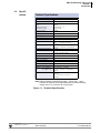
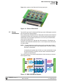
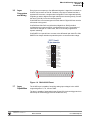
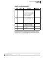
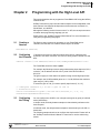
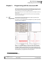
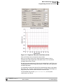
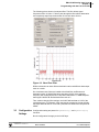
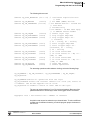
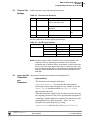
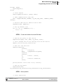
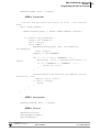
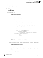
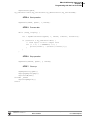
PowerDNA DNA/DNR-AI-205
Analog Input Layer
–
User Manual
Simultaneous Sampling, 18-bit,
4-channel, 250 kS/s per channel,
Analog Input Layer
June 2010 Edition
Version 3.9
PN Man-DNx-AI-205-0610
© Copyright 1998-2010 United Electronic Industries, Inc. All rights reserved.
i
No part of this publication may be reproduced, stored in a retrieval system, or transmitted, in any form
by any means, electronic, mechanical, by photocopying, recording, or otherwise without prior written
permission.
Information furnished in this manual is believed to be accurate and reliable. However, no responsibility
is assumed for its use, or for any infringements of patents or other rights of third parties that may result
from its use.
All product names listed are trademarks or trade names of their respective companies.
See UEI’s website for complete terms and conditions of sale:
http://www.ueidaq.com/company/terms.aspx
Contacting United Electronic Industries
Mailing Address:
27 Renmar Avenue
Walpole, MA 02081
U.S.A.
For a list of our distributors and partners in the US and around the world, please see
http://www.ueidaq.com/partners/
Support:
Telephone:
Fax:
(508) 921-4600
(508) 668-2350
Also see the FAQs and online “Live Help” feature on our web site.
Internet Support:
Support
Web-Site
FTP Site
[email protected]
www.ueidaq.com
ftp://ftp.ueidaq.com
Product Disclaimer:
WARNING!
DO NOT USE PRODUCTS SOLD BY UNITED ELECTRONIC INDUSTRIES, INC. AS CRITICAL
COMPONENTS IN LIFE SUPPORT DEVICES OR SYSTEMS.
Products sold by United Electronic Industries, Inc. are not authorized for use as critical components in
life support devices or systems. A critical component is any component of a life support device or
system whose failure to perform can be reasonably expected to cause the failure of the life support
device or system, or to affect its safety or effectiveness. Any attempt to purchase any United Electronic
Industries, Inc. product for that purpose is null and void and United Electronic Industries, Inc., accepts
no liability whatsoever in contract, tort, or otherwise, whether or not resulting from our or our
employees' negligence or failure to detect an improper purchase.
NOTE: Specifications shown in this document are subject to change without notice. Check with
UEI for current status.
ii
iii
Table of Contents
Chapter 1 Introduction
.................................................... 1
1.1
Organization of this manual . . . . . . . . . . . . . . . . . . . . . . . . . . . . . . . . . . . . . . . . . . . . 1
1.2
Conventions . . . . . . . . . . . . . . . . . . . . . . . . . . . . . . . . . . . . . . . . . . . . . . . . . . . . . . . . 1
1.3
The AI-205 Layer . . . . . . . . . . . . . . . . . . . . . . . . . . . . . . . . . . . . . . . . . . . . . . . . . . . . 2
1.4
Specifications . . . . . . . . . . . . . . . . . . . . . . . . . . . . . . . . . . . . . . . . . . . . . . . . . . . . . . . 3
1.5
Device Architecture. . . . . . . . . . . . . . . . . . . . . . . . . . . . . . . . . . . . . . . . . . . . . . . . . . . 4
1.6
Layer Connectors and Wiring . . . . . . . . . . . . . . . . . . . . . . . . . . . . . . . . . . . . . . . . . . . 5
1.7
Layer Capabilities . . . . . . . . . . . . . . . . . . . . . . . . . . . . . . . . . . . . . . . . . . . . . . . . . . . 5
1.8
Data Representation . . . . . . . . . . . . . . . . . . . . . . . . . . . . . . . . . . . . . . . . . . . . . . . . . . 6
Chapter 2 Programming with the High Level API . . . . . . . . . . . . . . . . . . . . . . . . . . . . . . . 8
2.1
Creating a Session . . . . . . . . . . . . . . . . . . . . . . . . . . . . . . . . . . . . . . . . . . . . . . . . . . . 8
2.2
Configuring the Channels . . . . . . . . . . . . . . . . . . . . . . . . . . . . . . . . . . . . . . . . . . . . . . 8
2.3
Configuring the Timing . . . . . . . . . . . . . . . . . . . . . . . . . . . . . . . . . . . . . . . . . . . . . . . . 8
2.4
Configuring the FIR Filters . . . . . . . . . . . . . . . . . . . . . . . . . . . . . . . . . . . . . . . . . . . . . 9
2.5
Reading Data . . . . . . . . . . . . . . . . . . . . . . . . . . . . . . . . . . . . . . . . . . . . . . . . . . . . . . . 9
2.6
Cleaning-up the Session. . . . . . . . . . . . . . . . . . . . . . . . . . . . . . . . . . . . . . . . . . . . . . . 9
Chapter 3 Programming with the Low-Level API . . . . . . . . . . . . . . . . . . . . . . . . . . . . . . 10
3.1
FIR Programming . . . . . . . . . . . . . . . . . . . . . . . . . . . . . . . . . . . . . . . . . . . . . . . . . . . 10
3.2
Configuration Settings. . . . . . . . . . . . . . . . . . . . . . . . . . . . . . . . . . . . . . . . . . . . . . . . 13
3.3
Channel List Settings . . . . . . . . . . . . . . . . . . . . . . . . . . . . . . . . . . . . . . . . . . . . . . . . 15
3.4
Layer-specific Commands and Parameters . . . . . . . . . . . . . . . . . . . . . . . . . . . . . . . 15
3.5
Data Representation in ACB and DMap . . . . . . . . . . . . . . . . . . . . . . . . . . . . . . . . . . 16
3.6
Using Layer in ACB Mode. . . . . . . . . . . . . . . . . . . . . . . . . . . . . . . . . . . . . . . . . . . . . 16
3.7
Using Layer in DMap Mode . . . . . . . . . . . . . . . . . . . . . . . . . . . . . . . . . . . . . . . . . . . 19
Appendix . . . . . . . . . . . . . . . . . . . . . . . . . . . . . . . . . . . . . . . . . . . . . . . . . . . . . . . . . . . . . . . . 21
Index
. . . . . . . . . . . . . . . . . . . . . . . . . . . . . . . . . . . . . . . . . . . . . . . . . . . . . . . . . . . . . . . . . . 23
© Copyright 2010
United Electronic Industries, Inc.
Tel: 508-921-4600
Date: June 2010
www.ueidaq.com
Vers: 3.9
File:DNA-AI-205TOC.fm
iv
Table of Figures
Chapter 1 Introduction . . . . . . . . . . . . . . . . . . . . . . . . . . . . . . . . . . . . . . . . . . . . . . . . . . . . 1
1-1
Technical Specifications ................................................................................................ 3
1-2
Photo of DNA-AI-205 ..................................................................................................... 4
1-3
DNA-AI-205 Block Diagram ........................................................................................... 4
1-4
DNA-AI-205 Pinout ........................................................................................................ 5
Chapter 2 Programming with the High Level API . . . . . . . . . . . . . . . . . . . . . . . . . . . . . . . 7
(None)
Chapter 3 Programming with the Low Level API . . . . . . . . . . . . . . . . . . . . . . . . . . . . . . . 9
3-1
ScopeFIR Display of Low-Pass Filter Characteristics.................................................. 10
3-2
Polyphase Filter with Cutoff above 4 kHz .................................................................... 12
3-3
Band Pass Filter........................................................................................................... 13
© Copyright 2010
United Electronic Industries, Inc.
Tel: 508-921-4600
Date: June 2010
www.ueidaq.com
Vers: 3.9
File:DNA-AI-205LOF.fm
DNx-AI-205 Analog Input Layer
Chapter 1
Introduction
Chapter 1
Introduction
This document outlines the feature set and use of the DNx-AI-205 layer. The
DNA version is an analog input module for the PowerDNA I/O Cube. The DNR
version is an analog input module for UEI HalfRACK and RACKtangle chassis.
1.1
Organization This DNx AI-205 User Manual is organized as follows:
of this manual
• Introduction
This chapter provides an overview of PowerDNA Analog Input Series
board features, the various models available, and what you need to get
started.
1.2
Conventions
•
Chapter 1 — The AI-205 layer
This chapter provides an overview of the device architecture,
connectivity, and logic of the AI-205 layer.
•
Programming Using the UeiDaq Framework High-Level API
This chapter provides an overview of the how to create a session,
configure the session for analog input, and interpret results on the
AI-205 series layer.
•
Programming Using the Low-Level API
This chapter describes Low-level API commands for configuring and
using the AI-205 series layer.
•
Appendix A: Accessories
This appendix provides a list of accessories available for AI-205
layer(s).
•
Appendix B: Calibration
This appendix outlines a layer calibration procedure for the AI-205
series layer.
•
Index
This is an alphabetical listing of the topics covered in this manual.
To help you get the most out of this manual and our products, please note that
we use the following conventions:
Tips are designed to highlight quick ways to get the job done, or reveal good
ideas you might not discover on your own.
NOTE: Notes alert you to important information.
CAUTION! Caution advises you of precautions to take to avoid
injury, data loss, and damage to your boards or a system crash.
Text formatted in bold typeface generally represents text that should be entered
verbatim. For instance, it can represent a command, as in the following
example: “You can instruct users how to run setup using a command such
as setup.exe.”
© Copyright 2010
United Electronic Industries, Inc.
Tel: 508-921-4600
Date: June 2010
www.ueidaq.com
Vers: 3.9
File: AI205 Chap1.fm
1
DNx-AI-205 Analog Input Layer
Chapter 1
Introduction
1.3
The AI-205
Layer
© Copyright 2010
United Electronic Industries, Inc.
AI-205 is an analog input layer with the following features:
•
Maximum sampling rate of 250kHz per channel
•
±100V max input range
•
18-bit resolution, no missing codes
•
Simultaneous sampling
•
75 kHz input bandwidth (75 kHz RC Filter on each analog input)
•
Polyphase filtering (three 128-tap hardware FIR filters with
post-decimators and bypass mode)
•
Four (4) analog input differential channels fully isolated from the system
ground (up to 500V) – and isolated between channels (up to 350V)
•
Gains of 1/10/100/1000, per-channel selectable, effective ranges:
±100V, ±10V, ±1V, ±0.1V
•
Over-voltage protection (150V)
•
2kV Electrostatic Shock Discharge (ESD) protection
•
2048 sample input FIFO with 32-bit per-sample timestamp
•
Interrupt request on any position in the input or channel list FIFO
•
On-layer EEPROM to store configuration and calibration data
•
Power consumption ~ 1.6/2.2W
•
Two bidirectional lines for every analog input channel. Line state is
encoded into analog input data
•
Two DIO lines per channel, DIO0 is configured by default as an output
and DIO1 as an input
Tel: 508-921-4600
Date: June 2010
www.ueidaq.com
Vers: 3.9
File: AI205 Chap1.fm
2
DNx-AI-205 Analog Input Layer
Chapter 1
Introduction
1.4
Specifications
Technical Specifications:
Max Sampling Rate
Number of Channels
DIOs per channel
FIR Unit:
Size
Decimation Ratio
Number of Taps
FIR Coefficient
Onboard FIFO Size
Input Ranges
Input Impedance
Input Bias Current
Input Bandwidth
Isolation
Input Overvoltage
Total Harmonic Distortion
ENOBs @ G=1:
Signal/(N+D) ratio
Integral Non-linearity
Channel Crosstalk
Power Consumption
Physical Dimensions
Operating Temp. (tested)
Operating Humidity
Vibration IEC 60068-2-6
IEC 60068-2-64
Shock
IEC 60068-2-27
250 kHz/channel
4 (individual A/D per channel)
2
3 stages
1-128 (default - 5)
128 per stage
loadable
2048 samples
±100V, ±10V, ±1V, ±0.1V
2 MΩ (to ground); 4 MΩ (differential)
±1.5 nA
75 kHz
350Vrms (between channels)
500Vrms (to system ground)
2000V ESD, ±150V overvoltage
protection (powered or unpowered)
–100 dB
18 bits @ 10 Hz (filtered)
17.1 bits @ 60 kHz (native)
100 dB
2.5 LSB
120 dB
3W
3.875 x 3.875”(98 x 98 mm)
-40°C to +85°C
95%, non-condensing
5 g, 10-500 Hz, sinusoidal
5 g (rms), 10-500 Hz, broad-band
random
50 g, 3 ms half sine, 18 shocks @ 6
orientations
30 g, 11 ms half sine, 18 shocks @ 6
orientations
Note: DIOs are default configured as: DIO0 – output, DIO1 – input.
Direction of each can be changed statically, but not dynamically.
Output (3.3V TTL) can drive up to 20 mA max.
Figure 1-1. Technical Specifications
© Copyright 2010
United Electronic Industries, Inc.
Tel: 508-921-4600
Date: June 2010
www.ueidaq.com
Vers: 3.9
File: AI205 Chap1.fm
3
DNx-AI-205 Analog Input Layer
Chapter 1
Introduction
Figure 1-2 is a photo of the DNA-AI-205 Analog Input layer.
Figure 1-2. Photo of DNA-AI-205
1.5
Device
Architecture
The AI-205 Layer has a PL-60x base (FPGA layer) and a 205 daughter card with
A/D converters and optical isolation.
Every channel has a dedicated FIR unit. Each FIR unit consists of three identical
in-hardware FIR filters and a decimator. An FIR filter has the ability to perform
multiplication and accumulation operations in one clock cycle. Each FIR filter
can be set into bypass state.
A FIR filter can accept up to 128 taps with 16-bit resolution. A Decimator can
decimate output data with coefficients from 1 to 32. Please see the FIR section
for further details.
NOTE: To avoid aliasing, the sampling rate should be greater than 100 kHz
(preferably about 200 kHz). Lower sampling rates, if needed, should be
achieved via decimation.
At sampling rates greater than 100 kHz, you must use decimation to get
the data rate down to 100 kHz or less in order to meet the maximum
transfer rate specification.
The AI-205 employs a successive approximation 18-bit converter per channel
with no pipeline delay.
Control
Logic
EEPROM
32-bit 66-MHz bus
Isolated
DC/DC
FIR Queue
decimation
128 taps
decimation
128 taps
128 taps
128 taps
18-bit
ADC
decimation
CH3 IN-
128 taps
CH3 IN+
3-Stage FIR Unit
decimation
Calibration
128 taps
...
decimation
18-bit
ADC
Optical Isolation
PGA
CH0 IN-
PGA
Analog Input Connector
CH0 IN+
decimation
3-Stage FIR Unit
Calibration
Figure 1-3. DNA-AI-205 Block Diagram
© Copyright 2010
United Electronic Industries, Inc.
Tel: 508-921-4600
Date: June 2010
www.ueidaq.com
Vers: 3.9
File: AI205 Chap1.fm
4
DNx-AI-205 Analog Input Layer
Chapter 1
Introduction
1.6
Layer
Connectors
and Wiring
Every layer can accept up to four differential signals. A signal line is marked as
CHx IN+ and a return as CHx IN-. Because every layer is isolated and has a
separate A/D converter, a single-ended configuration is not supported implicitly.
If signals you wish to digitize are single-ended (have common ground), connect
the return (CHx IN-) line to the common ground.
CHx AGND line is an isolated ground for this channel. Digital I/O lines are also
referenced to this ground.
CHx DIO0 and CHx DIO1 are bidirectional digital lines. DIO0 is default
configured as an output and DIO1 is configured as an input. The direction of
each can be changed on a static basis, but is not currently supported for
dynamic switching.
CHx SHIELD is a special line to connect to the differential pair shield.The CHx
SHIELD line always maintains a potential equal to a common-mode voltage.
DB-37 (female)
37-pin connector:
N/C
CH0 DIO1
CH0 AGND
CH0 INCH0 SHIELD
CH1 AGND
CH1 DIO0
CH1 AGND
CH1 IN+
N/C
CH2 DIO1
CH2 AGND
CH2 INCH2 SHIELD
CH3 AGND
CH3 DIO0
CH3 AGND
CH3 IN+
37
36
35
34
33
32
31
30
29
28
27
26
25
24
23
22
21
20
19
18
17
16
15
14
13
12
11
10
9
8
7
6
5
4
3
2
1
N/C
CH0 AGND
CH0 DIO0
CH0 AGND
CH0 IN+
N/C
CH1 DIO1
CH1 AGND
CH1 INCH1 SHIELD
CH2 AGND
CH2 DIO0
CH2 AGND
CH2 IN+
N/C
CH3 DIO1
CH3 AGND
CH3 INCH3 SHIELD
Figure 1-4. DNA-AI-205 Pinout
1.7
Layer
Capabilities
The AI-205 layer is capable of acquiring analog input voltages in the ±100V
range with gains of 1, 10, 100 and 1000.
The layer is capable of generating its own CL and CV clocks and trigger and can
also accept an external trigger from the SYNCx bus only.
© Copyright 2010
United Electronic Industries, Inc.
Tel: 508-921-4600
Date: June 2010
www.ueidaq.com
Vers: 3.9
File: AI205 Chap1.fm
5
DNx-AI-205 Analog Input Layer
Chapter 1
Introduction
The layer does not have hardware capability of analog triggering at present, but
will have a digital implementation (after conversion data analysis) in a future
revision.
Table 1-1. Gains
Card
Bandwidth
Gain
Range
Noise, LSB
Resolution,
(Noise
Limited at
High Gains)
DNA-AI-205
1 Mhz
1
± 100V
0.81
762µV
100 kHz
10
±10V
1.05
76.2µV
10 kHz
100
±1V
1.58
20µV
1 kHz
1000
±100mV
3.32
10µV
Analog two-pole anti-aliasing filtering is tuned to provide roll-off at 100kHz.
1.8
Data
Representation
The DNA-AI-205 layer is equipped with four 18-bit A/D converters. The layer can
return 18-bit straight binary data in 32-bit words combined with levels on
general-purpose digital I/O lines.
The 18-bit data is represented as follows:
Table 1-2. 18-bit Data Representation
Bit
Name
Description
Reset State
17-0
ADCDATA
Upper 18 bits of data,
straight-binary
<pos>
<pos> represents a position in the output buffer. Upon reset, every entry in the
output buffer is filled with its relative position number. If you start receiving
consecutive data from the layer, such as 0,1,2, etc., it means that either the layer
is not initialized properly or the layer is damaged.
To convert data into floating point, use the following formula (at a gain of 1):
Volts = (Raw & 3ffff) * (200V/2^18) – 100V
© Copyright 2010
United Electronic Industries, Inc.
Tel: 508-921-4600
Date: June 2010
www.ueidaq.com
Vers: 3.9
File: AI205 Chap1.fm
6
DNx-AI-205 Analog Input Layer
Chapter 1
Introduction
32-bit data has a different representation, as follows:
Table 1-3. 32-bit Data Representation
Bit
Name
Description
Reset State
31-28
CHN
AI-205 channel #
0
27
DIO1
Input level of DIO1 line. This line 0
is configured as an input by
default. User can switch it to an
output on a static basis before
startup, but cannot switch
direction dynamically.
26
DIO0
Input level of DIO0 line. This line 0
is configured as an output by
default. User can switch it to an
input on a static basis before
startup, but cannot switch
direction dynamically.
25-24
INFO
Additional information bits.
Reserved, in the future will
include status of level trigger
23-18
RSV
Reserved, should be ignored by
user application
17-0
ADCD
ADC conversion result
0
Because all channels have a separate converter and, potentially, a different
decimation ratio, the user application should rely on the CHN bits to determine
the channel to which a data point belongs.
© Copyright 2010
United Electronic Industries, Inc.
Tel: 508-921-4600
Date: June 2010
www.ueidaq.com
Vers: 3.9
File: AI205 Chap1.fm
7
DNx-AI-205 Analog Input Layer
Chapter 2
Programming with the High Level API
Chapter 2
Programming with the High Level API
This section describes how to program the PowerDNA AI-205 using the UeiDaq
Framework API.
UeiDaq Framework is object oriented and its objects can be manipulated in the
same manner from different development environments such as Visual C++,
Visual Basic, or LabVIEW.
Although the following section focuses on the C++ API, the concept is the same
no matter what programming language you use.
Please refer to the “UeiDaq Framework User Manual” for more information on
using other programming languages.
2.1
Creating a
Session
The Session object controls all operations on your PowerDNA device.
Therefore, the first task is to create a session object, as follows:
CUeiSession session;
2.2
Configuring
the Channels
Framework uses resource strings to select which device, subsystem and
channels to use within a session. The resource string syntax is similar to a web
URL:
<device class>://<IP address>/<Device Id>/<Subsystem><Channel list>
For PowerDNA, the device class is pdna.
For example, the following resource string selects analog input channels 0,2,3,4
on device 1 at IP address 192.168.100.2: “pdna://192.168.100.2/Dev1/
Ai0,2,3,4”
The gain to apply on each channel is specified using low and high input limits.
For example, the AI-205 available gains are 1, 10,100,1000 and the maximum
input range is [-100V, 100V].
To select the gain of 100, you need to specify input limits of [-1V, 1V].
// Configure channels 0,1 to use a gain of 100 in
// differential mode
session.CreateAIChannel(“pdna://192.168.100.2/Dev0/Ai0,1”, -1.0, 1.0,
UeiAIChannelInputModeDifferential);
2.3
Configuring
the Timing
You can configure the AI-205 to run in simple mode (point by point) or buffered
mode (ACB mode).
In simple mode, the delay between samples is determined by software on the
host computer.
In buffered mode, the delay between samples is determined by the AI-205 onboard clock.
The following sample shows how to configure the simple mode. Please refer to
the “UeiDaq Framework User’s Manual” to learn how to use the other timing
modes.
© Copyright 2010
United Electronic Industries, Inc.
Tel: 508-921-4600
Date: June 2010
www.ueidaq.com
Vers: 3.9
File: AI205 Chap2.fm
8
DNx-AI-205 Analog Input Layer
Chapter 2
Programming with the High Level API
session.ConfigureTimingForSimpleIO();
2.4
Configuring
Each AI-205 analog input channel is equipped with a three-stage FIR filter and
the FIR Filters decimator. You can control those filters using custom properties (Please read
the “UeiDaq Framework User Manual Appendix B).
Note that each property must be written in the sequence described below:
•
“channel”: An integer representing the channel for which you want to
configure the FIR filter.
•
“stage”: An integer set to 0, 1 or 2 representing the stage to configure for
the selected channel.
•
“decimation”: An integer representing the decimation for the selected
stage.
•
“tap”: An array of floating-point values representing the taps for the
selected stage. The maximum number of taps is 128.
NOTE: If all 128 cefficients are specified, the first coefficient should be set to 0.
Note that setting a decimation value greater than 1 will slow down the rate at
which your application will receive data from the AI-205. You need to adjust the
session timeout parameter accordingly.
The following sample code shows how to program the first stage of the FIR filter
on channel 0:
int firChannel = 0;
int firStage = 0;
int decimation = 1;
double taps[8]= {…};
MySession.SetCustomProperty(“channel”, sizeof(int), &firChannel);
MySession.SetCustomProperty(“stage”, sizeof(int), &firStage);
MySession.SetCustomProperty(“decimation”, sizeof(int), &decimation);
MySession.SetCustomProperty(“tap”, 8*sizeof(double), taps);
2.5
Reading Data Reading data from the AI-205 is done using a reader object. There is a reader
object to read raw data coming straight from the A/D converter. There is also a
reader object to read data already scaled to volts.
The following sample code shows how to create a scaled reader object and read
samples.
// Create a reader and link it to the session’s stream
CueiAnalogScaledReader reader(session.GetDataStream());
// read one scan, the buffer must be big enough to contain
// one value per channel
double data[2];
reader.ReadSingleScan(data);
2.6
Cleaning-up
the Session
The session object will clean itself up when it goes out of scope or when it is
destroyed. However, you can manually clean up the session (to reuse the object
with a different set of channels or parameters).
session.CleanUp();
© Copyright 2010
United Electronic Industries, Inc.
Tel: 508-921-4600
Date: June 2010
www.ueidaq.com
Vers: 3.9
File: AI205 Chap2.fm
9
DNx-AI-205 Analog Input Layer
Chapter 2
Programming with the High Level API
© Copyright 2010
United Electronic Industries, Inc.
Tel: 508-921-4600
Date: June 2010
www.ueidaq.com
Vers: 3.9
File: AI205 Chap2.fm
10
DNx-AI-205 Analog Input Layer
Chapter 3
Programming with the Low-Level API
Chapter 3
Programming with the Low-Level API
This section describes how to program the PowerDNA cube using the low-level
API. The low-level API offers direct access to the PowerDNA DAQBios protocol
and also allows you to access device registers directly.
We recommend that you use the UeiDaq Framework (see Chapter 2), which is
easier to use.
You should only need to use the low-level API if you are using an operating
system other than Windows.
3.1
FIR1
We recommend use of an external application capable of generating filter
Programming coefficients and visualizing filter data.
For example, you can use ScopeFIR from IOWegian Corp., which can produce
a display as shown in Figure 3-1.
Figure 3-1. ScopeFIR Display of Low-Pass Filter Characteristics
To design an FIR filter, you should first decide on a base sampling frequency.
The higher the base sampling frequency, the more taps you need to filter lower
frequency signals. On the other hand, a higher sampling frequency allows better
anti-aliasing filtering. A polyphase filter solves this problem.
1. Finite Input Response digital filter.
© Copyright 2010
United Electronic Industries, Inc.
Tel: 508-921-4600
Date: June2010
www.ueidaq.com
Vers: 3.9
File: AI205 Chap3.fm
10
DNx-AI-205 Analog Input Layer
Chapter 3
Programming with the Low-Level API
The second consideration is the filter type. A FIR filter can be programmed to
perform low-pass, high-pass, band-pass and band-stop filtering. A Low-pass
filter (shown) allows signals with frequencies lower than selected to pass. A
High-pass filter does the opposite. A Band-pass filter allows only certain
frequencies to pass through and a band-stop filter blocks them.
Pass-band frequency defines which frequencies the filter should pass without
attenuation. Stop-band defines at what frequency the desired attenuation should
be achieved. The filter requires more taps to achieve sharper roll-off curve.
Pass-band ripple defines deviations of the signal amplitude on signal frequency.
To decrease pass-band ripple, use more filter taps.
Stop-band attenuation defines the remaining signal level at stop-band
frequencies.
To define a band-pass or a band-stop filter, you should define center frequency
and pass-band width (symmetrical to center frequency).
Each AI-205 filter has 128 taps. It might not be enough to filter a user signal
when a low pass-band frequency is required along with steep roll-off. To achieve
this kind of filtering, you should design a polyphase filter in FIR unit filters and
decimators.
For example, if you want to sample at 100 kHz (to avoid picking up aliases) but
the signal of interest lies below 50Hz, you could use the filter displayed in
Figure 3-2.
© Copyright 2010
United Electronic Industries, Inc.
Tel: 508-921-4600
Date: June2010
www.ueidaq.com
Vers: 3.9
File: AI205 Chap3.fm
11
DNx-AI-205 Analog Input Layer
Chapter 3
Programming with the Low-Level API
Figure 3-2. Polyphase Filter with Cutoff above 4 kHz
First, the FIR filter cuts out frequencies above 4 kHz.
Now you can safely remove all the signal frequencies above 5 kHz by
decimating the original signal with a decimation ratio of 10. The effective
sampling rate becomes 10 kHz.
By setting the same parameters for the second and third filter in the FIR unit, the
resulting signal will have a sampling frequency of 100Hz with 10Hz pass-band
and 40Hz stop-band.
It is impossible to achieve this kind of filter characterizing using a single-phase
filter with 3*128 = 384 taps. Polyphase filters have a significant advantage over
single-phase filters with the same cumulative number of taps.
The PowerDNA API provides DqAdv205LoadCoeff()to set up filter
coefficients for an FIR unit.
© Copyright 2010
United Electronic Industries, Inc.
Tel: 508-921-4600
Date: June2010
www.ueidaq.com
Vers: 3.9
File: AI205 Chap3.fm
12
DNx-AI-205 Analog Input Layer
Chapter 3
Programming with the Low-Level API
The following picture shows a band-pass filter. This filter allows signal
frequencies from 13 kHz to 17 kHz to pass through the filter without attenuation
and completely stops frequencies below 10 kHz and above 20 kHz.
Figure 3-3. Band Pass Filter
Different channels can have different decimation ratios and different data output
rates as a result.
On a hardware reset, filters are loaded with default filter coefficients and
decimation ratios. A default filter has a pass-band of 20% of the sampling
frequency with a stop-band at 25%. Stop-band attenuation is –80dB and passband ripple 0.00001 dB. Default decimation ratio is 5.
Thus, without changing filter settings, the AI-205 delivers data at 1/125 of the
original frequency. For example, if the user sets the conversion clock at 125 kHz,
the output data rate will be 1 kHz with a pass-band at 200Hz and a stop-band at
250Hz.
3.2
Configuration Configuration setting are passed in DqCmdSetCfg() and DqAcbInitOps()
functions.
Settings
Not all configuration bits apply to the AI-205 layer.
© Copyright 2010
United Electronic Industries, Inc.
Tel: 508-921-4600
Date: June2010
www.ueidaq.com
Vers: 3.9
File: AI205 Chap3.fm
13
DNx-AI-205 Analog Input Layer
Chapter 3
Programming with the Low-Level API
The following bits are used:
#define DQ_FIFO_MODEFIFO (2L << 16) // continuous acquisition with
// FIFO
#define DQ_LN_MAPPED
(1L<<15)
// For WRRD (DMAP) devices
#define DQ_LN_STREAMING (1L<<14)
// For RDFIFO devices - stream the
// FIFO data
// automatically
// For WRFIFO - do NOT send reply
// to WRFIFO unless needed
#define DQ_LN_IRQEN
(1L<<10)
// enable layer irqs
#define DQ_LN_PTRIGEDGE1 (1L<<9)
// stop trigger edge MSB
#define DQ_LN_PTRIGEDGE0 (1L<<8)
// stop trigger edge: 00 // software,
// 01 - rising, 02 - falling
#define DQ_LN_STRIGEDGE1 (1L<<7)
// start trigger edge MSB
#define DQ_LN_STRIGEDGE0 (1L<<6)
// start trigger edge: 00 //software, 01 - rising,
// 02 - falling
#define DQ_LN_CVCKSRC1
(1L<<5)
// CV clock source MSB
#define DQ_LN_CVCKSRC0
(1L<<4)
// CV clock source 01 - SW, 10 //HW, 11 -EXT
#define DQ_LN_CLCKSRC1
(1L<<3)
// CL clock source MSB
#define DQ_LN_CLCKSRC0
(1L<<2)
// CL clock source 01 - SW, 10 //HW, 11 -EXT
#define DQ_LN_ACTIVE
(1L<<1)
// "STS" LED status
#define DQ_LN_ENABLED
(1L<<0)
// enable operations
For streaming operations with hardware clocking, select the following flags:
DQ_LN_ENABLE | DQ_LN_CVCKSRC0 | DQ_LN_STREAMING | DQ_LN_IRQEN |
DQ_LN_ACTIVE
DQ_LN_ENABLE enables all operations
DQ_LN_CVCKSRC0 selects the internal
a timebase. The AI-205 supports the
DQ_LN_ACTIVE is needed to switch on
with the layer
channel list clock (CL) source as
CV clock.
“STS” LED on CPU layer.
The user can select either the CL or CV clock as a timebase. Because of the
parallel architecture of AI-205 layer, either clock triggers all four converters.
Aggregate rate = Per-channel rate * Number of channels
Acquisition rate cannot be selected on per-channel basis. To select a different
resulting rate for different channels, you should program proper decimators in
the FIR unit.
© Copyright 2010
United Electronic Industries, Inc.
Tel: 508-921-4600
Date: June2010
www.ueidaq.com
Vers: 3.9
File: AI205 Chap3.fm
14
DNx-AI-205 Analog Input Layer
Chapter 3
Programming with the Low-Level API
3.3
Channel List
Settings
AI-205 layer has a very simple channel list structure:
Table 3-1. Channel List Structure
Bit
Name
Purpose
31
DQ_LNCL_NEXT Tells firmware that there is next
entry in the channel list
20
DQ_LNCL_TSRQ Request timestamp as a next
data point
11..8
Gain Number (see Table 3-2)
7..0
Channel number
Macro
DQ_LNCL_GAI
N()
Gains are different for different options of AI-205 layer
Table 3-2. AI-205 Layer Options\
Layer Type
Range
Gain
Gain Number
DNA-AI-205
±100V
1
0
±10V
10
1
±1V
100
2
±100mV
1000
3
NOTE: Despite having the same conversion rate across all channels, data
output rate can vary, depending on decimation. Even when the
decimation ratio is identical, there is no guarantee in which order data
will be put into the output buffer. That’s why you should not rely on the
order of channels he specified in the channel list, but rather strip output
data into channel data based on channel numbers embedded in the
data itself.
3.4
Layer-specific Layer-specific functions are described in the DaqLibHL.h file.
Commands
• DqAdv205Read()
and
This function works using the underlying
Parameters
DqReadAIChannel(), but converts data using internal
knowledge of input range and gain of every channel. It uses the
DQCMD_IOCTL command with the DQIOCTL_CVTCHNL
function under the hood.
When this function is called for the first time, the firmware stops
any ongoing operation on the device specified and reprograms it
accordingly with the channel list supplied. The function uses the
preprogrammed CL update frequency – 10Hz. You can
reprogram the update frequency by calling
DqCmdSetClk()after the first call to DqAdv205Read().
© Copyright 2010
United Electronic Industries, Inc.
Tel: 508-921-4600
Date: June2010
www.ueidaq.com
Vers: 3.9
File: AI205 Chap3.fm
15
DNx-AI-205 Analog Input Layer
Chapter 3
Programming with the Low-Level API
Thus, the user cannot perform this function call when the layer is
involved in any streaming or data mapping operations.
If you specify a short timeout delay, this function can time out
when called for the first time, because it is executed as a pending
command and layer programming takes up to 10ms.
Once this function is called, the layer continuously acquires data
and every call to the function returns the latest acquired data.
If you would like to cancel ongoing sampling, call the same
function with 0xffffffff as a channel number.
•
DqAdv205LoadCoeff()
This function loads the coefficient table.
3.5
Data
Representation in ACB
and DMap
Output layer data are presented in ACB in raw or floating point format in
voltages. Raw data are represented as 32-bit words and floating point data are
represented as structures.
typedef struct {
uint32 raw;// raw part of the data including channel number
double data;// converted data
} DQly205_double, *pDQly205_double;
3.6
Using Layer
in ACB Mode
This is a pseudo-code example that highlights the functions needed in sequence
to use ACB on the 205 layer. A complete example with error checking can be
found in the directory SampleACB205.
Note: the AI-205 layer is not guaranteed to return the channels in the correct
order. This is why data returned from the DqAcbGetScansCopy() function is
an array of DQly205_float structures, which contain both the raw and
converted channel values. The upper 4 bits of the raw value tell you which
channel the value came from. Our example does not use this value to sort the
data; it just dumps out the data in the order received.
#include "PDNA.h"
// unit configuration word
#define CFG205
(DQ_LN_ENABLED \
|DQ_LN_ACTIVE \
|DQ_LN_GETRAW \
|DQ_LN_IRQEN \
|DQ_LN_CVCKSRC0 \
|DQ_LN_STREAMING \
|DQ_AI205_MODEFIFO)
uint32 Config = CFG205;
STEP 1: Start DQE engine
© Copyright 2010
United Electronic Industries, Inc.
Tel: 508-921-4600
Date: June2010
www.ueidaq.com
Vers: 3.9
File: AI205 Chap3.fm
16
DNx-AI-205 Analog Input Layer
Chapter 3
Programming with the Low-Level API
#ifndef _WIN32
DqInitDAQLib();
#endif
// Start engine
DqStartDQEngine(1000*1, &pDqe, NULL);
// Open communication with IOM
hd0 = DqOpenIOM(IOM_IPADDR0, DQ_UDP_DAQ_PORT, TIMEOUT_DELAY,
&RdCfg);
// Receive IOM crucial identification data
DqCmdEcho(hd0, DQRdCfg);
// Set up channel list
for (n = 0; n < CHANNELS; n++) {
CL[n] = n;
}
STEP 2: Create and initialize host and IOM sides.
// Now we are going to test device
DqAcbCreate(pDqe, hd0, DEVN, DQ_SS0IN, &bcb);
// Let’s assume that we are dealing with AI-201 device
dquser_initialize_acb_structure();
// Now call the function
DqAcbInitOps(bcb,
&Config,
0,
//TrigSize,
NULL,
//pDQSETTRIG TrigMode,
&fCLClk,
&CVSize,
0,
//float* fCLClk,
CL,
0,
//uint32* ScanBlock,
&acb);
printf("Actual clock rate: %f\n", fCVClk);
// Now set up events
DqeSetEvent(bcb,
DQ_eFrameDone|DQ_ePacketLost|DQ_eBufferError|DQ_ePacketOOB);
STEP 3: Start operation.
// Start operations
© Copyright 2010
United Electronic Industries, Inc.
Tel: 508-921-4600
Date: June2010
www.ueidaq.com
Vers: 3.9
File: AI205 Chap3.fm
17
DNx-AI-205 Analog Input Layer
Chapter 3
Programming with the Low-Level API
DqeEnable(TRUE, &bcb, 1, FALSE);
STEP 4: Process data.
// We will not use event notification at first - just retrieve
scans
while (keep_looping) {
DqeWaitForEvent(&bcb, 1, FALSE, EVENT_TIMEOUT, &events);
if (events & DQ_eFrameDone) {
minrq = acb.framesize;
avail = minrq;
while (TRUE) {
DqAcbGetScansCopy(bcb, data, acb.framesize,
acb.framesize,
&size, &avail);
samples += size*CHANNELS;
for (i = 0; i < size * CHANNELS; i++) {
fprintf(fo, "%f\t", ((DQly205_float*)data + i)>data);
if ((i % CHANNELS) == (CHANNELS - 1)) {
fprintf(fo, "\n");
}
}
printf("eFD:%d scans received (%d samples) min=%d
avail=%d\n", size,
samples, minrq, avail);
if (avail < minrq) {
break;
}
}
}
}
STEP 5: Stop operation.
DqeEnable(FALSE, &bcb, 1, FALSE);
STEP 6: Clean up.
DqAcbDestroy(bcb);
DqStopDQEngine(pDqe);
DqCloseIOM(hd0);
© Copyright 2010
United Electronic Industries, Inc.
Tel: 508-921-4600
Date: June2010
www.ueidaq.com
Vers: 3.9
File: AI205 Chap3.fm
18
DNx-AI-205 Analog Input Layer
Chapter 3
Programming with the Low-Level API
#ifndef _WIN32
DqCleanUpDAQLib();
#endif
3.7
Using Layer
in DMap Mode
#include "PDNA.h"
STEP 1: Start DQE engine.
#ifndef _WIN32
DqInitDAQLib();
#endif
// Start engine
DqStartDQEngine(1000*10, &pDqe, NULL);
// open communication with IOM
hd0 = DqOpenIOM(IOM_IPADDR0, DQ_UDP_DAQ_PORT,
TIMEOUT_DELAY, &DQRdCfg);
// Receive IOM crucial identification data
DqCmdEcho(hd0, DQRdCfg);
for(i = 0; i < DQ_MAXDEVN; i++) {
if (DQRdCfg->devmod[i]) {
printf("Model: %x Option: %x\n", DQRdCfg>devmod[i], DQRdCfg->option[i]);
} else {
break;
}
}
STEP 2: Create and initialize host and IOM sides.
DqDmapCreate(pDqe, hd0, &pBcb, UPDATE_PERIOD, &dmapin, &dmapout));
STEP 3: Add channels into DMap.
for (i = 0; i < CHANNELS; i++) {
DqDmapSetEntry(pBcb, DEVN, DQ_SS0IN, i, DQ_ACB_DATA_RAW, 1,
&ioffset[i]);
}
DqDmapInitOps(pBcb));
© Copyright 2010
United Electronic Industries, Inc.
Tel: 508-921-4600
Date: June2010
www.ueidaq.com
Vers: 3.9
File: AI205 Chap3.fm
19
DNx-AI-205 Analog Input Layer
Chapter 3
Programming with the Low-Level API
DqeSetEvent(pBcb,
DQ_eDataAvailable|DQ_ePacketLost|DQ_eBufferError|DQ_ePacketOOB);
STEP 4: Start operation.
DqeEnable(TRUE, &pBcb, 1, FALSE);
STEP 5: Process data.
while (keep_looping) {
ret = DqeWaitForEvent(&pBcb, 1, FALSE, timeout, &eventsin);
if (eventsin & DQ_eDataAvailable) {
// read input or write output here
for (i = 0; i < CHANNELS; i++) {
printf("%08x ", *(uint32*)ioffset[i]);
}
}
}
STEP 6: Stop operation.
DqeEnable(FALSE, &pBcb, 1, FALSE);
STEP 7: Clean up.
DqDmapDestroy(pBcb);
DqStopDQEngine(pDqe);
DqCloseIOM(hd0);
#ifndef _WIN32
DqCleanUpDAQLib();
#endif
© Copyright 2010
United Electronic Industries, Inc.
Tel: 508-921-4600
Date: June2010
www.ueidaq.com
Vers: 3.9
File: AI205 Chap3.fm
20
DNx-AI-205 Analog Input Layer
Appendix
A. Appendix A Accessories
The following cables and STP boards are available for the AI-205 layer.
DNA-CBL-37
3ft, 37-way flat ribbon cable; connects DNA-AI-205 to panels
DNA-STP-37
37-way screw terminal panel
DNA-STP-37D
37-way direct-connect screw terminal panel
© Copyright 2010
United Electronic Industries, Inc.
Tel: 508-921-4600
Date: June 2010
www.ueidaq.com
Vers: 3.9
File: AI205 Appendix.fm
21
Index
23
Index
I
A
Accessories 21
Advanced Circular Buffer
Architecture 4
Input Mode
Differential 2, 5
Internet Support ii
16
B
L
Band Pass Filter 13
Block Diagram 4
Layer Capabilities
Low-Level API 10
C
M
Calibration 21
Calibration Procedure 21
Capabilities 5
Channel List
Structure 15
Cleaning-up the Session 9
Configuring the Channels 8
Configuring the FIR Filters 9
Configuring the Timing 8
Conventions 1
Creating a Session 8
D
Data Representation
Dedicated FIR 4
DMap 19
DNA-CBL-37 21
DNA-STP-37 21
DNA-STP-37D 21
Mailing Address
Mode
ACB 16
DMap 16
FIR 10
On-layer EEPROM 2
Organization 1
Over-voltage protection
Pinout 5
Polyphase Filter 12
Polyphase filtering 2
Product Disclaimer ii
16
R
Reading Data
S
H
T
Technical Specifications
The AI-205 Layer 2
8
3
U
Using Layer in ACB Mode 16
Using Layer in DMap Mode 19
6
High Level API
9
Sampling Rate 2
Specifications 3
Support ii
F
Gain(s) 2,
2
P
ESD protection 2
G
ii
O
E
Features 2
FIR filter 12
FPGA 4
Framework API
5
8
© Copyright 2010
United Electronic Industries, Inc.
Tel: 508-921-4600
Date: June 2010
www.ueidaq.com
Vers. 3.9
File:DNA-AI-205IX.fm