1
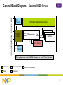
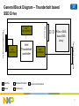
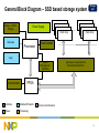
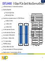
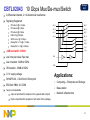
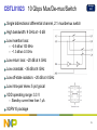
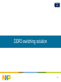
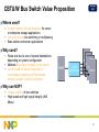
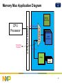
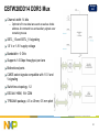
SSD Storage Application Presentation Interface Products 3Q 2012 Rev 1.0 Interface Products Overview System Management I2C-Bus Controllers I2C-Bus Buffers, Muxes & Switches GPIO Expanders LED Controllers Temperature Sensors Active & Passive Level Translation EEPROMs Electronic DIP Switches Stepper Motor Controllers Power Line Modem RF Transceivers High Speed Interface High Speed Buffers & Muxes SerDes Memory Interface UARTs Bridges SDIO Controller PCIe Phy Display Port Converters Clocks, Watches & Graphic Drivers Real Time Clocks Display Drivers Proximity / Touch Switches Data Converters Watch Chips No. 1 in I2C-bus product Most integrated DisplayPort adapters High speed switches up to 10 Gb/s No. 1 in low power RTC’s San Jose San Jose Zurich Focus on high-value, mixed-signal components to support key processors in high-growth connected markets 2 Internal SSD General Block Diagram – Internal SSD Drive SATA Connector Mini PCIe Connector OR mSATA connector ESD Protection SATA redriver PCIe redriver Internal or external power supply Host Interface Processor I2C Flash Interface Flash Array Temp. Sensor ESD Protection The system can have SATA interface or mini PCIe interface Interface Standard Products Power Processing Sensors and Actuators 3 General Block Diagram – External SSD Drive USB connector ESD Protection Thunderbolt Interface USB/TBT interface External SSD Internal or external power supply Host Interface Processor I2C Flash Interface Flash Array Temp. Sensor ESD Protection The system can have SATA interface or mini PCIe interface Interface Standard Products Power Processing Sensors and Actuators 4 General Block Diagram – Thunderbolt based SSD Drive PCIe out NXP CBTL05023 Intel Thunderbolt controller Interface Standard Products Power Processing NXP CBTL05023 PCIe or SATA based SSD Array Thunderbolt Connector Thunderbolt Connector NXP CBTL06DP211 T-Bolt SSD Sensors and Actuators 5 General Block Diagram – SSD based storage system Debug – UARTs, Bridges Power Supply …. Flash Array Discretes Processor Storage SSD Flash Array DDR3 NVDIMM Logic System Management (I2C/SPI) DDR3 NVDIMM High Speed Analog Switches SATA/mSATA/SAS/PCIe FPGA Interface Standard Products Power Processing Sensors and Actuators 6 Storage SSD High Speed Analog Switching Solutions 7 Storage SSD Uses Cases for PCIe PCH PCIe Slot Configuration – x16x8x4x2x1 CBTL04082 PCIe x 1 PCIe x 4 PCIe x 1 NEC µPD720200 USB 3.0 USB 3.0 Marvell 88SE6121 SATA 3 Gbps eSATA IDT 89HMPEB3 83ZA eSATA Intel Processor CBTL04082 CBTL04082 CBTL04082 CBTL04082 PCIe x 8 PCIe x 16 8 CBTU04082 5 Gbps Mux/De-mux/Switch Storage SSD 4 differential channel, 2 : 1 mux/demux Signaling Supported PCIe Gen2, USB3.0, SATA @ 5Gbps Insertion loss: -2dB at 3 GHz A0_P B0_P A0_N B0_N A1_P B1_P A1_N B1_N C0_P Low crosstalk: −23 dB at 3 GHz C0_N Low off-isolation: −23 dB at 3 GHz C1_P C1_N VDD operating range: 1.65 V to 2.0 V ESD tolerance: – 6 kV HBM I/O – 1 kV CDM Low bit-to-bit skew: 10 ps max (between positive and negative bits) A2_P B2_P A2_N B2_N A3_P B3_P A3_N B3_N C2_P Low channel-to-channel skew: 35 ps max C2_N C3_P HVQFN42 package C3_N SEL 9 CBTL04082 5 Gbps Mux/De-mux/Switch Storage SSD 4 differential channel, 2:1 bi-directional mux/demux Signaling Supported PCIe Gen2, USB3.0, SATA @ 5Gbps XSD01 VDD GND VDD VDD GND XSD01 39 39 40 40 41 41 42 42 -0.5dB at 100 MHz VDD Insertion loss -2.0dB at 2.5 GHz 38 GND A0_P 2 37 B0_N A0_N 2 37 B0_P A0_N 3 36 B1_P C0_P 3 36 B0_N GND 4 35 B1_N C0_N 4 35 GND VDD 5 34 C0_P A1_P 5 34 VDD A1_P 6 33 C0_N A1_N 6 33 B1_P A1_N 7 32 C1_P C1_P 7 32 B1_N 31 C1_N C1_N 8 30 VDD VDD 9 31 VDD 30 GND 10 29 B2_P A2_P SEL 10 29 A2_P 11 28 B2_N GND A2_N 11 28 B2_P A2_N 12 27 VDD 13 26 B3_P C2_P 12 27 B2_N B3_N C2_N 13 26 GND 14 VDD 25 C2_P A3_P 14 25 A3_P GND 15 24 C2_N A3_N 15 24 B3_P A3_N 16 23 C3_P C3_P 16 23 B3_N GND 17 22 C3_N C3_N 17 22 GND CBTL04082A CBTL04082B 21 9 20 8 SEL 19 VDD VDD XSD23 VDD GND GND VDD XSD23 VDD 3.3 V supply voltage 1 18 Off-isolation: -30dB at 2.5GHz A0_P 21 Low crosstalk: -30dB at 2.5GHz B0_P 20 Low inter-pair skew: 35ps max 38 19 Low intra-pair skew: 5ps max 1 18 -3.0dB at 4.3 GHz GND HVQFN42 package A0_P B0_P A0_N B0_N A1_P B1_P A1_N B1_N XSD01 C0_P C0_N C1_P C1_N A2_P B2_P A2_N B2_N A3_P B3_P A3_N B3_N C2_P XSD23 C2_N C3_P ESD 6kV HBM, 1kV CDM Two pin outs available for PCB layout optimization C3_N SEL Standby current < 10 uA controlled by XSD pin 10 Storage SSD CBTL02042 5 Gbps Mux/De-mux/Switch 2 differential channel, 2:1 bi-directional mux/demux Signaling Supported A0_P B0_P A0_N B0_N PCIe Gen1 @ 2.5Gbps A1_P B1_P PCIe Gen2 @ 5Gbps A1_N B1_N C0_P USB 3.0 @ 5.0Gbps C0_N SATA Gen 2 @ 3.0Gbps C1_P DisplayPort v1.1a @ 2.7Gbps -3dB bandwidth 4.3 GHz C1_N SEL Low inter-pair skew: 5ps max 3.3 V supply voltage DHVQFN 20, 2.5x4.5mm,0.5mm pitch ESD 6kV HBM, 1kV CDM Two pin-outs available A pin-out optimized for outputs on the opposite side of input VDD VSS 1 VDD 20 VSS Off-isolation: -30dB at 5GHz 1 XSD 20 Low crosstalk: -30dB at 5GHz XSD 2 19 B0_P XSD 2 19 C0_P VDD 3 18 B0_N VDD 3 18 C0_N A0_P 4 17 B1_P B0_P 4 17 A0_P A0_N 5 16 B1_N B0_N 5 16 A0_N VSS 6 15 C0_P VSS 6 15 C1_P CBTL02042A CBTL02042B A1_P 7 14 C0_N B1_P 7 14 C1_N A1_N 8 13 C1_P B1_N 8 13 A1_P SEL 9 12 C1_N SEL 9 12 A1_N 10 11 10 11 VSS VDD VDD VSS B pin-out optimized for outputs on both sides of the package 11 Storage SSD CBTU04083 8Gbps PCIe Gen3 Mux/De-mux/Switch 4 differential channel, 2 : 1 multiplexer/demultiplexer Signaling Supported PCIe Gen3 @ 8 Gbps SAS Gen2 @ 6 Gbps Insertion loss -2.8 dB at 4GHz Low crosstalk: −30 dB at 4 GHz Low off-isolation: −30 dB at 4 GHz VDD operating range: 1.65 V to 2.0 V ESD tolerance: 6kV HBM Low bit-to-bit skew: 10 ps max (between positive and negative bits) Low channel-to-channel skew: 35 ps max HVQFN42 package 12 Storage SSD CBTL04083 8 Gbps PCIe Gen3 Mux/De-mux/Switch 4 differential channel, 2:1 bi-directional mux/demux Signaling Supported PCIe Gen3 @ 8 Gbps SAS Gen2 @ 6 Gbps Insertion loss, equivalent to about 2” of FR4 PCB trace XSD01 VDD GND VDD VDD GND XSD01 39 1 38 B0_P A0_P 1 B1_P B1_N C0_P C0_N 38 GND A0_P 2 37 B0_N A0_N 2 37 B0_P A0_N 3 36 B1_P C0_P 3 36 B0_N GND 4 35 B1_N C0_N 4 35 GND VDD 5 34 C0_P A1_P 5 34 VDD A1_P 6 33 C0_N A1_N 6 33 B1_P A1_N 7 32 C1_P C1_P 7 32 B1_N VDD 8 31 C1_N C1_N 8 31 VDD SEL 9 30 VDD VDD 9 30 SEL GND 10 29 B2_P A2_P 10 29 GND A2_P 11 28 B2_N A2_N 11 28 B2_P A2_N 12 27 B3_P C2_P 12 27 B2_N VDD 13 26 B3_N C2_N 13 26 VDD GND 14 25 C2_P A3_P 14 25 GND CBTL04083A CBTL04083B B3_N GND 17 22 C3_N C3_N 17 22 GND 21 B3_P 23 20 24 16 19 15 C3_P 18 A3_N C3_P 21 C2_N 23 20 24 16 19 15 18 A3_P A3_N XSD23 VDD GND GND VDD XSD23 VDD ESD 2kV HBM, 500V CDM A1_P A1_N C1_P GND VDD HVQFN42 package 40 3.3 V supply voltage 41 Off-isolation: -10dB at 4GHz B0_P B0_N XSD01 42 Low crosstalk: -25dB at 4GHz 39 Low inter-pair skew: 20ps max 40 Low intra-pair skew: 5ps max 41 -3.0dB at 8 GHz 42 -1.0dB at 4 GHz VDD -0.5dB at 100 MHz A0_P A0_N C1_N A2_P B2_P A2_N B2_N A3_P B3_P A3_N B3_N C2_P XSD23 C2_N C3_P C3_N SEL Two pin outs available for PCB layout optimization Standby current < 10 uA controlled by XSD pin 13 CBTL02043 10 Gbps Mux/De-mux/Switch Storage SSD 2 differential channel, 2:1 bi-directional mux/demux Signaling Supported PCIe Gen1 @ 2.5 Gbps PCIe Gen2 @ 5 Gbps PCIe Gen3 @ 8 Gbps USB 3.0 @ 5.0Gbps SATA Gen 2 @ 3.0 Gbps DisplayPort v1.1a @ 2.7 Gbps DisplayPort v1.2 @ 5.4 Gbps A0_P B0_P A0_N B0_N A1_P B1_P A1_N B1_N C0_P C0_N C1_P -3dB bandwidth 10 GHz Low inter-pair skew: 5ps max C1_N SEL Low crosstalk: -30dB at 5GHz XSD Off-isolation: -30dB at 5GHz 3.3 V supply voltage DHVQFN 20, 2.5x4.5mm,0.5mm pitch ESD 6kV HBM, 1kV CDM Two pin-outs available A pin-out optimized for outputs on the opposite side of input Applications: Computing – Enterprise and Storage Base-station Network infrastructure B pin-out optimized for outputs on both sides of the package 14 CBTL01023 10 Gbps Mux/De-mux/Switch Storage SSD Single bidirectional differential channel, 2:1 mux/demux switch High bandwidth: 9 GHz at −3 dB Low insertion loss: – −0.5 dB at 100 MHz – −1.3 dB at 4.0 GHz Low return loss: −20 dB at 4 GHz Low crosstalk: −35 dB at 4 GHz Low off-state isolation: −20 dB at 4 GHz Low intra-pair skew: 5 ps typical VDD operating range: 3.3 V – Standby current less than 1 μA XQFN10 package 15 Storage SSD NXP High Speed Switches Portfolio PCIe Gen 2, USB 3.0, mSATA, LVDS, SATA 2.0, SAS 1.0 Product Function Samples Production CBTU04082B 5 Gbps PCIe Gen 2 Mux/De-mux/Switch NOW NOW NOW NOW NOW NOW (4 differential channels) CBTL04082A 5 Gbps PCIe Gen 2 Mux/De-mux/Switch CBTL04082B A and B pin outs optimized for PCB layouts (4 differential channels) CBTL02042A 5 Gbps PCIe Gen 2 Mux/De-mux/Switch CBTL02042B A and B pin outs optimized for PCB layouts (2 differential channels) 16 Storage SSD NXP High Speed Switches Portfolio PCIe Gen 3, SAS 2.0, SATA 3.0, USB 3.0 Product Function Samples Production CBTU04083B 8 Gbps PCIe Gen3 Mux/De-mux/Switch NOW NOW NOW NOW NOW NOW NOW NOW (4 differential channels) CBTL04083A 8 Gbps PCIe Gen3 Mux/De-mux/Switch CBTL04083B A and B pin outs optimized for PCB layouts (4 differential channels) CBTL02043A 10 Gbps Mux/De-mux/Switch CBTL02043B A and B pin outs optimized for PCB layouts (2 differential channels) CBTL01023 10 Gbps Mux/De-mux/Switch (1 differential channel) 17 Storage SSD DDR3 switching solution 18 CBTU/W Bus Switch Value Proposition Storage SSD Where used? • Custom memory bus architectures for server or enterprise storage applications • General purpose bus switching or multiplexing • Base station and server applications Why used? • Route one bus to one of several destinations depending on system configuration • Maintain high signal integrity at high speed • Can be used for failover purposes in servers/base-stations and Flash based memory support in high end servers Host CBTx Switch/mux Bank 1 Bank 1 Bank 1 Bank n Why use NXP? • Unique portfolio of bus switches • High speed and high signal integrity (800 Mbps) 19 Storage SSD Memory Mux Application Diagram Termination Resistors DIMM SOCKET CPU Processor 533/666/800 MHz CBTW28DD14 Battery/ SuperCap DDR DDR Memories DDR Memories DDR Memories Memories 300 MHz FPGA NAND NAND NAND NAND Flash Flash Flash Flash 20 CBTW28DD14 DDR3 Mux Storage SSD Channel width: 14 bits – Optimal to fit one data lane each as well as divide address & command bus and auxiliary signals over remaining muxes SSTL_15 and SSTL_18 signaling 1.5 V or 1.8 V supply voltage Bandwidth > 3 GHz Supports 1.6 Gbps throughput per lane Bidirectional ports CMOS select signals compatible with 1.5 V and 1.8 V signaling Switch/mux topology: 1:2 ESD 4kV HBM, 1kV CDM TFBGA48 package, 4.5 x 4.5mm, 0.5 mm pitch 21 External SSD T-Bolt SSD DisplayPort/Thunderbolt switches 22 CBTL05023 Thunderbolt Mux External SSD T-Bolt SSD CBTL05023 is optimized to interface TBT/miniDP connector for TBT applications Excellent Signal Integrity to support 5.4Gbps DP1.2 HBR2 data rate – -15dB DDRL @ 2.5GHz for DP MUX – -2dB DDIL @ 2.5GHz for DP MUX – 7GHz bandwidth with 3.3V common mode input voltage • Pass rail-to-rail LS signal swing without clipping Optimized Integration to work with external PIN diodes for 10Gbps+AUX/DDC MUX – BIASOUT buffer supports bias current up to 6 PIN diodes – Integrated bias R for PIN diode path HPD input buffer with 5V tolerant Small 3 mm X3 mm HVQFN24 package with 0.4mm pitch 23 CBTL06DP211 DPv1.1a Mux/De-mux/Switch 1 : 2 multiplexing External SSD T-Bolt SSD – – – – DisplayPort (v1.1 - 2.7 Gbit/s) or PCIe Gen1 (2.5 Gbps) 4 high-speed differential channels 1 channel 4:1 muxing for AUX differential signals or DDC clock and data – 1 channel 2:1 muxing for HPD Low intra-pair differential skew (< 5 ps) Low inter-pair skew (< 180 ps) Current Consumption – Operation – Shutdown 0.2 A < 10 mA DDC and AUX ports tolerant to being pulled to +5 V via 2.2 kΩ resistor – Supports HDMI/DVI incorrect dongle connection 24 Standard I2C Storage SSD building blocks Overview of all standalone peripherals VCC4 Stepper Motor Controller I2C AD or DA Converters I2C General Purpose I/O Expanders Custom I²C Slaves / Masters I2C DIP Switches VCC5 VCC0 VCC2 PCA9541A I2C Master Selector / Demux I2C Mulitplexers & Switches VCC3 I2C LED Blinkers / Dimmers Capacitive Sensors I2C Serial EEPROMs & RAM VCC1 I²C Bus Buffers, Hubs, Repeaters & Translators I²C in hardware or software emulation I²C Bus Controllers LCD Drivers (with I2C) µC Functions with I2C I2C Bus Enablers 8 I2C Real Time Clock / Calendar On-board Off-board µC I2C Temperature Sensors Custom I2C hardware or software emulated Other hardware Bridges (with I²C) Demo Boards & Support I 2C Fast Mode+ Products Click Here SPI UART On-board Off-board UART 25 I2 C Storage SSD NXP I2C Fast Mode Plus Devices – PCA96xx Bus speed DC to 1 MHz fully compatible with existing I2C and SMBus – Higher bandwidth allows more devices on the bus and more complicated patterns w/o addition of buffers Bus drive strength 10x normal I2C I/O drive w/o addition of buffers – Drive heavier capacitive load or longer cable lengths – Low cost alternative to USB, Ethernet, wireless New practical features – Software reset of I/O ports (via I2C bus) – Hardware reset pin – Hardware address pins connecting to VCC, GND, SCL, SDA allow up to 64 addresses vs the normal 8 using only three pins New NXP Cortex™ microcontrollers support Fast-mode plus Target applications: amusement/gaming, lighting, remote user interface applications (e.g. POS, security, kiosk, etc) I2C-bus Specification UM10204 at www.nxp.com/i2c 26 I2 C NXP Fast-mode Plus Product Offerings Bus Controller Bus Buffer LED Controller TYPE Device Device Device PCA9622 PCA9661 PCA9663 PCA9665 CHAN 16 Storage SSD GPIO OUTPUT (OD = Open Drain; TP = Totem Pole ) (mA) (V) OD 100 40 Device # I/O RESET PCA9672 8 YES PCA9621 8 NO PCA9624 8 OD 100 40 PCA9673 16 YES PCA9626 24 OD 100 40 PCA9674/74A 8 NO PCA9601 PCA9632 4 OD/TP 25/10 5 PCA9670 8 YES PCA9605 PCA9633 4 OD/TP 25/10 5 PCA9675 16 NO PCA9634 8 OD/TP 25/10 5 PCA9671 16 YES PCA9635 16 OD/TP 25/10 5 PCA9685 16 OD/TP 25/10 5 PCA9698 40 YES PCA9955 16 Constant Current 57 40 PCA9600 PCA9646 27 I2 C Storage SSD General Purpose I/O Expanders 28 I2 C Storage SSD I/O Expanders with Flexible Output Structures Quasi-Output Structure: - Strong PMOS transistor is turned on only during the LH transition and turned off during static drive - Weak pull-up current source (100μA) at the output - Used in low-power applications where the 100-μA drive is sufficient to bias the inputs of CMOS devices - May be reconfigured as an input or output without the need of a port configuration register # of Outputs 8 16 Interrupt Reset Interrupt & Reset 2Kbit EEPROM Interrupt and 2Kbit EEPROM PCF8574/74A, PCA8574/74A, PCA9674/74A PCA9670 PCA9672 PCA9500/58 PCF8575/75C, PCA9675 PCA9671 PCA9673 - PCA9501 - Totem-Pole Output Structure: - Upper PMOS transistor is turned on during LH transition and static high drive. Up to 10mA (or 25mA) of high drive - Some devices have weak pull-up resistors at the output - Used in applications requiring high drive for heavy loads - Extra command byte needed to switch an I/O pin between input and output # of Outputs None Reset Interrupt Interrupt and Reset 4 8 16 PCA9536 PCA9534/54/54A PCA9535/35C/55 PCA9538, PCA9502, PCA9574 - PCA9557 - 40 - - PCA9537 PCA9539/39R, PCA9575 PCA9505/06, PCA9698 29 Flexible I/O (Output) Structures Quasi Output Totem-Pole Output I2 C Storage SSD Open-Drain Output Strong PMOS on for ½ SCL VCC VCC I/O 100 uA Output input ~25 mA ~10 mA R* I/O input input ~25 mA ~25 mA • Strong PMOS transistor is turned on only during the LH transition • Upper PMOS transistor is turned on during static high drive • PMOS transistor is off during static drive • Some devices have weak pull-ups at the output • No upper PMOS transistor • No pull-up resistor • No weak current drive • Weak current source at the output 30 New Low Voltage GPIO Family I2 C Storage SSD Purpose Offer lower voltage GPIO that operate down to 1.65V but still operate up to 5.5V Offer new input latch and other new Agile IO features with “L” in part number Easy migration - Drop in replacement for existing PCA95XX GPIO PCA Name Feature 16 bit Single Vcc INT & PU PCA9555A INT PCA9535A INT & RST PCA9539A Two Vcc INT & PU INT INT & RST Input Latch Input Latch Input Latch PCAL9555A PCAL9535A PCAL9539A INT & RST INT & RST Input Latch PCA6416A PCAL6416A 31 I2 C Storage SSD Benefit of Lower VCC and Wider VCC Range VVDD2 DD (1.8 (2.3 V) PCA9655L PCA9555 IO0_0 VDD IO0_1 IO0_2 IO0_3 I/O Ports VDD1 (1.8 V) IO0_4 IO0_5 IO0_6 VDD IO0_7 Host CPU IO1_0 SCL SDA GPIO GND Translator (PCA9306) IO1_1 SCL IO1_2 SDA IO1_3 INT A2 A1 A0 I/O Ports IO1_4 GPIO Application IO1_5 IO1_6 IO1_7 VSS Lower VCC to 1.65V on GPIO supply eliminates the need for a voltage translator like the PCA9306! 32 I2 C Storage SSD Benefit of Lower VCC and Wider VCC Range VVDD2 DD (1.8 V) PCA9655L PCA9555A IO0_0 VDD IO0_1 IO0_2 IO0_3 I/O Ports VDD1 (1.8 V) IO0_4 IO0_5 IO0_6 VDD IO0_7 Host CPU IO1_0 SCL SCL SDA SDA GPIO INT GND IO1_1 IO1_2 IO1_3 A2 A1 A0 I/O Ports IO1_4 GPIO Application IO1_5 IO1_6 IO1_7 VSS Lower VCC to 1.65V on GPIO supply eliminates the need for a voltage translator like the PCA9306 and second set of pull ups! 33 Features of the PCAL64xx IO Expanders I2 C Storage SSD GPIO are backwards compatible to existing GPIOs with new superset of registers to control the configurable features. The PCA64xxA and PCA95xxA devices will be drop in replacements while the PCAL64xxA and PCAL95xxA will offer these desirable features: GPIO input latch (bit by bit – default not latched): Lock I/O pin changes on input until the register is read. GPIO output drive strength control (bit by bit – default 10 mA push and 25 mA pull): User can program I/O drive strength 25%, 50%, 75% or 100% This output can be used to control the brightness of LEDs. GPIO open drain control (24-bit bit by bit and 8 and 16-bit bank by bank – default push pull): Provide an optional open-drain output for each I/O pin. This output can also provide an additional wired-OR plane. GPIO pull up or pull down (bit by bit – default no PU/PD): User can turn on/off an internal pull-up or pull down on each I/O pin. GPIO interrupt mask and interrupt status (bit by bit – default not masked): User can enable or disable interrupts of each I/O pin. Identifies the source of interrupts of each I/O pin. 5 state address pins to allow more devices on the bus (24 bit only) 34 I2 C Storage SSD PCA6416A Two Vcc Low-voltage, 16-bit I2C-bus I/O expander with interrupt output, reset, and configuration registers Features • Operating Power-Supply Voltage Range of 1.65 V to 5.5 V • Low Standby Current Consumption of 3 uA Maximum • Allows Bidirectional Voltage-Level Translation and GPIO Expansion Between 1.8, 2.5, 3.3 or 5 V SCL/SDA and 1.8, 2.5, 3.3, or 5 V Totem Pole configured I/O Port • Schmitt-Trigger Hysteresis of 10% of SCL/SDA Supply Voltage • Noise Filter on SCL/SDA Inputs • Fast Mode I2C Bus Operating Frequency of up to 400-kHz • Active-Low Reset Input • Open-Drain Active-Low Interrupt Output • 5-V Tolerant I/O Ports • High current Drive for Directly Driving LEDs • Input/Output Configuration Register • Polarity Inversion Register • Internal Power-On Reset • Power-Up With All Channels Configured as Inputs • No Glitch On Power-Up • Package – 24 pin TSSOP, HWQFN and CSP • Latch-Up Performance Exceeds 100 mA per JESD 78, Class II • ESD Protection Exceeds JESD 22 – 2000-V Human-Body Model (A114-A) – 1000-V Charged-Device Model (C101) 35 I2 C Storage SSD LED Controllers 36 I2C I2 C LED Switch, Blinkers, Dimmers, and Controllers Storage SSD Product overview Fast-mode Plus I2C Bus LED Switch (GPIOs) I2C Bus LED Blinkers 2 slow PWMs PCA967x family PCA955x family Fast-mode Plus I2C Bus I2C Bus LED Controllers LED Dimmers 2 fast PWMs Fast PWM on every output Global PWM for dim or blink PCA953x family PCA962x & 3x families 37 LED Controller Portfolio I2 C OUTPUT Part # #of channel VS CC Storage SSD FUNCTION VDD IDD Control I/F PWM Function PCA9901 1 5V 20mA 1-Wire 12 bit indiv Blinker PCA9922 8 5V 60mA Serial in/out 12-bit indiv Blinker PCA9550,3,1,2 2,4,8,16 - 5V 25mA 400kHz Fm 8-bit Indiv Blinker PCA9530,3,1,2 2,4,8,16 - 5V 25mA 400kHz Fm 8-bit Indiv Dimmer PCA9633,4,5* 4,8,16 - 5V 25mA 1 MHZ Fm+ 8-bit Indiv/global Dimmer 4 (low power) - 5V 25mA 1 MHZ Fm+ 8-bit Indiv/global Dimmer 8,16,24 - 40V 100mA 1 MHZ Fm+ 8-bit Indiv/global Dimmer PCA9685* 16 - 5V 25mA 1 MHZ Fm+ 12 bit indiv Dimmer PCA9952,5** 16 40V 57mA 1 MHZ Fm+ 8-bit Indiv/global Dimmer PCU9654,5,6 8,16,24 40V 100mA 5 MHZ UFM 8-bit Indiv/global Dimmer 40V 57mA 5 MHZ UFM 8-bit Indiv/global Dimmer PCA9632 PCA9624,2,6 PCU9955 16 - 38 I2 C Storage SSD Bus Buffers & Level Shifters 39 I2C Bus Buffer Portfolio Repeaters PCA9527 PCA9515/15A PCA9509 SO SO SO SO 0.9 – to 5.5V PCA9507 RTA for HDMI PCA9519 4 x PCA9509 NO PCA9605 PCA9646 30-mA Drive; 1:4-Channel SO PCA9522[1] IO PCA9508 SO PCA9512A/12B IO Active Level Shifter NO P82B96 [2] P82B715 SO AM No Static Offset PCA9511A PCA9600/9601 SO 1-MHz Speed IO 0.6-V Threshold 30-mA Drive Processor to SMBus PCA9517A PCA9525 (Long Cable Drivers) Active Level Shifter 3-mA Drive Processor to SMBus PCA9509P SO 5-Channel Hub Expander Processor to SMBus PCA9509A PCA9518A SO Storage SSD Extenders (Long Cable) Hot-Swap Buffers SO PCA9507 + ½ PCA9517 I2 C NO PCA9514A IO 0.8-V Threshold PCA9513A IO NO = No Offset 92-mA Current Source SO = Static Offset SO PCA9510A IO No Accelerator IO = Incremental Offset AM = Amplifier [1] PCA9522 is compliant for ATCA applications [2] P82B96 is widely used for opto-isolation applications Red part = 1 MHz system 40 Level Translators Portfolio Active Level Shifter - input & Output dual supply - Capacitance Isolation - High Noise Margins PCA9527 SO RTA for HDMI PCA9519 4 x PCA9509 PCA9508 - Capacitance Isolation P82B96 Passive Level Shifter - No capacitance Isolation - Low Power & Low Cost SO PCA9306 NO 1 – 5.5V PCA9518A 2.3 – 5.5V AM GTL2002/03/10/00 NO 1 – 5.5V SO PCA9600/9601 SO NVT20xx NO 1 – 5.5V w low Ron 0.9 – to 5.5V PCA9507 - Single Supply Storage SSD SO Processor to SMBus PCA9517A Active level Shifter 2.2 – 15V PCA9507 + ½ PCA9517 PCA9509/A/P I2 C SO SO SO 2.2 – 15V PCA9522 1.8 -10V w/HS PCA9516A 2.3 – 5.5V IO SO NO = No Offset SO = Static Offset Active Level Shifter PCA9512A/12B Active Level Shifter IO IO = Incremental Offset AM = Amplifier Red text = 1 MHz system 41 Active Level-Shifter Value Proposition I2 C Storage SSD Why used? – Voltage level shifting between host processor’s I2C-bus and peripheral devices when there is a mismatch of supply voltages – Used when additional drive is needed or to isolate two sections of the bus loading Where used? – Digital logic level translation between host processor and slave device where capacitance isolation is required Why NXP Level-Shifter? – Largest selection of active and passive level shifters – Continuous innovation with new NXP voltage follower and zero-offset active buffers NXP Level Shifter Portfolio Device Description Normal I/O Static Level Offset I/O Accelerator Idle Stop Detect for Hotswap Interrupt PCA9507 2.7V-to-5.5V Level Shifter A Side B Side PCA9508 0.9V-to-5.5V Level Shifter with Offset Free Hot-Swap A Side B Side PCA9509 1.0V-to-5.5V Level Shifter B Side A Side 2KV PCA9515A 3.3V / 5.0V I2C-Bus Repeater A & B Sides 2KV PCA9516A 5-Channel I2C Bus Hub A & B Sides 2KV PCA9517A 0.9V-to-5.5V Level Shifter B Side 5KV PCA9518A 5-Channel I2C Bus Hub Expander A & B Sides 2KV PCA9519 1.1V-to-5.5V Quad Level Shifter B Side A Side 2KV PCA9527 3.0V-to-5.5V Level Shifter A Side B Side PCA9617 0.8V-to-5.5V Level Shifter A Side B Side A Side × (A-Side) ESD (HBM) 5KV × × (A-Side) 6KV × 8KV 5KV 42 PCA9509 0.95V-to-3.3V/5V Level Shifting Buffer I2 C Storage SSD Features Bidirectional level shift between 0.95V and 3.3V/5V without directional control pin A-Side Static Offset Low Voltage B-Side Normal I2C Levels (SMBus/5V) Processor SMBus / Cable Isolates noise and bus capacitance Support dual Vcc(A) and Vcc(B) – Vcc(A) ranges from 0.95V to Vcc(B)-1V – Vcc(B) ranges from 3V to 5.5V Low static level offset (200mV) on A side No external pull-up required on A side due to internal current source MSOP8 and 1.6 x 1.6 “GM” package ESD – 2000 V HBM per JESD22-A114 – 200 V MM perJESD22-A115 – 1000 V CDM per JESD22-C101 Ideal for 1.0 V ± 5% master controlling 3.3V/5V slave or vice-versa 43 Passive Level-Shifter Value Proposition I2 C Storage SSD Why used? – Voltage level shifting between host processor’s I2C-bus peripheral devices when there is a mismatch of supply voltages – Used when additional drive is not needed and capacitive loading is not an issue Where used? – Digital logic level translation between host processor and slave device; no direction control and no capacitance isolation are required – Applications requiring open-drain bidirectional or unidirectional voltage translation (down to 1V) without a direction pin Why NXP Passive Level-Shifter? – Largest selection of active and passive level shifters – Continuous innovation with new NXP Voltage Translation family (NVT20xx) in widths of 1, 2, 3, 4, 6, 8 and 10 bits NXP Passive Level-Shifter Portfolio Device Description RON Process ESD (HBM) PCA9306 2-Bit Bidirectional Voltage-Level Translator 3.5 W CMOS 2kV GTL2002 2-Bit Bidirectional Voltage-Level Translator 6.5 W BiCMOS >2kV GTL2003 8-Bit Bidirectional Voltage-Level Translator 6.5 W BiCMOS >2kV GTL2010 10-Bit Bidirectional Voltage-Level Translator 6.5 W BiCMOS >2kV GTL2000 22-Bit Bidirectional Voltage-Level Translator 6.5 W BiCMOS >2kV NVT2001/02/03/04/ 06/08/10 x-Bit Bidirectional Voltage-Level Translator 3.5 W BiCMOS >4kV 44 PCA9306 Storage SSD I2 C Bidirectional I2C-Bus & SMBus Level Translator Features Bi-directional without need for direction pin Voltage translation between any voltage from 1.0 V to 5.5 V Lock-up free operation for isolation when EN = LOW Mixed-mode I2C-bus application: run two buses, one at 400 kHz other at 100 kHz operating frequency Excellent ESD performance 3.3 V 3.3 V 1.2 V GND VREF1 RPU PCA9306 1.5 V RPU 200K 1.8 V RPU Voltage Level Translation – Mixed-mode I2C-Bus Applications 2.5 V RPU Applications EN VREF2 VCC VCC I2C SCL SCL1 SCL2 SCL BUS MASTER GND I2C BUS DEVICE SDA SDA1 SDA2 SDA GND 45 I2 C NVT20xx: Level Translator Family Where used? – Digital Logic level translation – TI’s PCA9306 is drop-in replacement for NXP GTL2002 and PCA9306 Storage SSD # CH New OLD Usage 1 NVT2001 -- Clock 2 NVT2002 PCA9306 GTL2002 I 2C Why used? – Voltage level shifting in range of 1V and 5V – Bi-directional without direction pin 3 NVT2003 -- I2C, server 4 NVT2004 -- SPI 6 NVT2006 -- Why NXP NVT 20xx Level Shifter? – More consistent device naming - NVT means “NXP Voltage Translator” o NVT2001 – 1-bit o NVT2002 – 2-bit (alt source GTL2002) o NVT2003 - 3-bit o NVT2004 – 4-bit o NVT2006 – 6-bit o NVT2008 – 8-bit (alt source GTL2003) o NVT2010 – 10-bit (alt source GTL2010) – In TSSOP and smaller packages – Can be used as FET replacement – Continuous innovation from NXP 8 NVT2008 GTL2003 Digital RGB 10 NVT2010 GTL2010 Data Bus 22 -- GTL2000 46 I2 C Storage SSD Multiplexers, Demultiplexers & Switches 47 What are Multiplexers and Switches I2 C Storage SSD Application Note AN262 MUX I2C Bus 0 OFF I2C I2C Bus 1 Bus Interrupt 0 I2C Controller Interrupt 1 Interrupt Out Master Channel active after STOP command 2, 4, 8 channel I2C Bus 0 OFF I2C I2C Bus 1 Bus Reset Interrupt Out OFF I2C Controller Interrupt 0 Interrupt 1 Switch 48 Multiplexer / Switch Family Mux/Switches Family 2:1 Mux/Switches 4:1 Mux/Switches Mux /w Interrupt PCA9544A Mux PCA9540B Mux /w Interrupt PCA9542A Switch /w Interrupt & Reset PCA9545A/B/C* I2 C Storage SSD Master Selector Interrupt & Reset PCA9541A/01, /03 8:1 Mux/Switch Mux /w Reset PCA9547 Switch /w Reset PCA9548A Switch /w Reset PCA9546A Switch /w Interrupt & Reset PCA9543A/B/C* * Buffered Switch /w Reset (Fm+) PCA9646 Note: A, B, and C have different I2C fixed address 49 I2 C External SSD Internal SSD Storage SSD Temperature Sensors 50 Temperature Sensors Value Proposition External SSD I2 C Internal SSD Storage SSD Where used? – Networking platforms, Backplanes, Notebook and Tablets Why used? – Determine the temperature – Set window for Interrupt, alarm, fan control, shutdown, etc. Part # Accuracy SMBus Timeout LM75A / 75B ±2 ˚C A = No; B = Yes SE95 ±1 ˚C No SE98A ±1 ˚C Yes SE97B* ±1 ˚C Yes Why NXP Thermal Sensor? – Large selection of commonly used local sensor and local/remote sensor thermal sensors in a wide range of packages – Invented the I2C-bus. Continuously developing newer devices with added features to support different applications. – Continuous innovation with new low price LM75B local sensor in small 2 x 3 mm package wire local local Remote Diode Sensor Local Sensor Accuracy Remote Sensor Accuracy NE1617A ±2 ˚C ±3 ˚C NE1619** ±3 ˚C ±5 ˚C SA56004 ±2 ˚C ±1 ˚C Part # Note: * With 2Kbit EEPROM; ** With voltage monitors 51 Temp Sensor in SSD Applications High Density Memory Array (Flash) I2 C External SSD Internal SSD Storage SSD Power-hungry Controller High current Switched-mode Power Supply Temp Sensor for thermal management 52 I2 C Thermal Sensor Portfolio External SSD Internal SSD Storage SSD ±1°C Remote, ±2°C Local, 11-bit ADC A c c u r a c y DDR3 SPD, ±1°C, 11-bit ADC, 2K EEPROM Low Voltage, ±1°C, 11-bit ADC SE98A SE95 SA56004 SE97B Improved ±1°C LM75, Local, 11-bit ADC ±3°C Remote, ±2°C Local, 8-bit ADC HECETA Voltage Monitor NE1617A LM75A NE1619 LM75B Industry Standard, , ±2°C Local, 11-bit ADC Local only Remote & Local Remote & Local with Voltage Monitor Complexity Samples Now 53 I2 C NXP Temp Sensor Selection Table External SSD Internal SSD Storage SSD Temp Resolution / A/D Resolution Bits Power Supply Voltage Range Supply Current Operating uA Supply Current Standby uA Package Option 0.125/11 2.8-5.5 1000 3.5 SO8 TSSOP8 LM75B 1 ±2°C 0.125/11 2.8-5.5 300 1 SO8, TSSOP8 XSON8, HWSON8 SE95 1 ±1°C 0.125/11 2.8-5.5 NE1617A 1 1 ±2°C ±3°C 1.0/8 3.0-5.5 70 3.0 QSOP16 NE1619 1 1* ±3°C ±5°C 1.0/8 2.8-5.5 500 100 QSOP16 SA56004 1 1 ±2°C ±1°C 0.125/11 3.0-5.5 500 10 SO8, TSSOP8, HVSON8 SE97B 1 ±1°C 0.125/11 3.0-3.6 400 3 HWSON8 SE98A 1 ±1°C 0.125/11 1.7-3.6 400 5 TSSOP8, HWSON8 Accuracy Remote (max) ±2°C Accuracy Local (max) Local Channels 1 Remote Channels Part Number LM75A SO8, TSSOP8 * NE1619 monitor different power supplies: 12 V, 5 V, 3.3 V, 2.5 V, VCCP, VDD 54 LM75B Local Digital Temp. Sensor & Thermal Watchdog I2 C External SSD Internal SSD Storage SSD Features Pin-for-pin replacement for industry standard LM75 and LM75A I2C-bus interface - 8 devices on the same bus Power supply range from 2.8 V to 5.5 V Temperatures range from -55 °C to +125 °C Frequency range 20 Hz to 400 kHz with bus fault time-out to prevent hanging up the bus 11-bit ADC - temperature resolution of 0.125 °C Temperature accuracy of: ±2 °C from -25 °C to +100 °C ±3 °C from -55 °C to +125 °C Programmable temperature threshold and hysteresis set points Max supply current of 1.0 µA in shutdown mode Stand-alone operation as thermostat at power-up ESD protection exceeds 4500 V HBM per JESD22A114, 450 V MM per JESD22-A115 and 2000 V CDM per JESD22-C101 Small 8-pin package types: SO8, TSSOP8, XSON8, & HWSON8 55 I2 C Storage SSD Bridges 56 What is a Bridge IC? I2 C Storage SSD New generation of interface solutions for managing communication among various bus interfaces The purpose is to overcome the limitations of the host bus interface to the peripherals UART UART I2C I2C SPI IrDA SPI GPIO Benefit : – – – – Greater design flexibility Ability to retain original design investment Faster time to market Link legacy and new systems and vice versa 57 NXP Bridges Value Proposition I2 C Storage SSD Why used? • To provide an extra serial port, a SPI or I2C controller. • To bridge between two different buses: SPI to I2C, I2C to SPI, etc. • Three to five wires host interface connection Where used? • Telecommunication network routers, Servers, Blades Why NXP Bridges? • Low cost, advanced low profile packages and easy to use solutions • Sample demo boards and sample software code or drivers are available • NXP offers extensive application support including on-line technical support: [email protected] UART UART I2C I2C SPI IrDA SPI GPIO 58 I2 C Selecting a Bridge IC TO FROM I2C UART UART Storage SSD SPI SC18IM700 SC16IS740 SC16IS75x SC16IS76x SC16IS850L I2C SPI I2C/SPI-to-UART Bridges SC18IS602B SC18IS600 SC16IS740IPW/Q900 Part # UART FIFO SPI GPIO SC16IS740 1 64 4Mbps – SC16IS750 1 64 4Mbps 8 SC16IS752 2 64 4Mbps 8 SC16IS760 1 64 15Mbps 8 SC16IS762 2 64 15Mbps 8 SC16IS850L 1 128 15Mbps – Fully featured standalone UART (IrDA) with I2C/SPI interface and 64byte FIFOs; -40°C to +85°C; TSSOP24; AEC-Q100 compliant automotive qualification SPI-to-I2C Bridges Part # SPI I2C GPIO CLK SC18IS600 1Mbps 400kHz 4 Int I2C-to-SPI Bridges UART-to-I2C Bridge Part # UART I2C GPIO CLK Part # SPI I2C GPIO CLK SC18IM700 460.8kbps 400kHz 8 Int SC18IS602B 1.8Mbps 400kHz 4 Int 59 I2 C Storage SSD UARTs 60 Commercial 16CxxxB UART Family Features I2 C Storage SSD Benefits One-stop shopping Widest supply range (2.5V, 3.3V, 5V) at industrial temperature range (-40˚C to 85˚C) without price premium Single part can be used for multiple systems and multiple operating environments. Lower overall cost of ownership – can replace up to four competitor parts. Fastest device on the market with over 20% faster bus cycle times and baud rates up to 5Mbps Compatible with high-speed processors Power-down mode Ideal for battery-operated systems HVQFN and BGA package options Ideal for small, portable systems Windows and Linux OS-compatible Simplifies software development Infrared (IrDA) interface Enables wireless, short-range applications Software readily available Shortens design cycle Automatic software and hardware flow control Reduces CPU overhead and data loss DMA mode and wide variety of FIFO depths Increases system throughput Drop-in compatibility with existing 16C devices Alternative source to other manufacturers Number of Channels Broad line of single to quad channel UARTs SC16C654B SC16C754B 4 SC16C554B 2 SC68C2550B SC16C2550B SC16C2552B SC68C652B SC16C652B SC68C752B SC16C752B 1 SC16C550B SC16C650B SC16C750B 16 32 FIFO Depth (Bytes) 64 61 I2 C Support Tools 62 I2C2005-1 Demonstration Board Kit I2 C Features Easy experimentation and training. I2C-bus I/O Ports, Temperature Sensors, LED Drivers, Real-time Clock daughter cards Use USB to Windows PC/Laptop GUI/power See details in User Manual Order kits at www.demoboard.com or eTools 63 I2C I2 C Fm+ Development Kit Features Modular evaluation board for Fast-mode Plus (Fm+) devices Easy experimentation and training board Used to develop software and evaluate device performance USB connections for direct control of device with GUI Standalone processor for developing code to control device Used in conjunction with associated daughter cards for GPIO Expanders, LED Controllers, Temperature Sensors, Bus Buffers, etc. Board in development Daughter Cards may also be used with I2C-2005 Board 64 I2 C Sales Collateral I2C-bus device tri-fold I2C GPIO tri-fold High speed switches tri-fold LED controller tri-fold Doc. # 9397 750 16987 Doc. #: 9397 750 17144 Doc. # 9397 750 17037 Doc. # 9397 750 16950 65 I2 C Technical Contact Product Information: www.ics.nxp.com NXP Technical Support: www.nxp.com/support/ E-mail: [email protected] 66