1
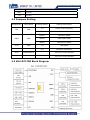
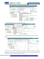
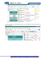
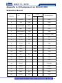
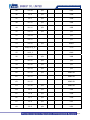
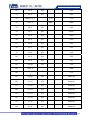
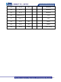
www.embedinfo.com/en EM-LPC1700 Evaluation Board User Manual V1.2 EMBEST CO., LIMITED Address:Room 509, Luohu Science & Technology Building, #85 Taining Road, Shenzhen, Guangdong, China 518020 Telephone: 0086-755-25621715 or 25635626 ext. 1715 Fax: 0086-755-25616057 E-mail: [email protected] || [email protected] Website: http://www.embedinfo.com/en 1/21 www.embedinfo.com/en Content CHAPTER 1 OVERVIEW ...............................................................3 1.1 Product List includes .....................................................4 1.2 Getting Start................................................................4 1.3 Jumpers ......................................................................5 CHAPTER 2 M-LPC1700 HARDWARE SPECIFICATION ..........................6 2.1 Board Overview............................................................6 2.2 Jumpers Setting ...........................................................7 2.3 EM-LPC1700 Block Diagram ...........................................7 2.4 Power Supply ...............................................................8 2.5 Clock Source................................................................8 2.6 Audio ..........................................................................8 2.7 UART ..........................................................................8 2.8 SD Card Interface.........................................................9 2.9 CAN Connector........................................................... 10 2.10 Human-Computer Interface (LCD) ............................. 10 2.11 Hardware Testing...................................................... 11 CHAPTER 3 SOFTWARE DEVELOPMENT AND EXAMPLES ......................... 14 3.1 MDK Introduction ....................................................... 14 3.2 Example Operation ..................................................... 14 APPENDIX A: IO ASSIGNMENT ON EM-LPC1700 EVALUATION BOARD...... 17 2/21 www.embedinfo.com/en Chapter 1 Overview EM-LPC1700 is the latest generation of full function evaluation board produced by Embest for NXP ARM Cortex-M3 core-based processors. The board features comprehensive interfaces, which not only provides a good platform for application development, but also is the first choice for learners. Combining with our company's debugging tools ULINK2, it will offer you a better development environment for saving time and improving efficiency. The features of EM-LPC1700: • Processors: NXP LPC17xx*, the frequency up to 100MHz • Internal Memory: up to 512KB flash memory, 64KB SRAM • 2 RS232 Interfaces • 2 CAN Interfaces • 1 Ethernet Interface • 1 JTAG Interface • 1 ETM Interface • 2 Cortex Debug Interfaces • 1 LCD Display • 1 USB Device/Host/OTG Interface • 1 Analog Output (connected to speaker by default) • 1 Analog Input (connected to potentiometer by default) • RTC (with back-up battery) • 1 Mini SD Card Interface * Note: EM-LPC1700 Evaluation Board is available in three variants: the LPC1758, LPC1766 and LPC1768. • The LPC1758 board (Order# P758): Processor is populated with the NXP LPC1758 microcontroller, 512KB Flash memory, 80 pins, 100MHz. • The LPC1766 (Order# P766): Processor is populated with the NXP LPC1766 microcontroller, 256KB Flash memory, 100 pins, 100MHz. • The LPC1768 (Order# P768): Processor is populated with the NXP LPC1768 microcontroller, 512KB Flash memory, 100 pins, 100MHz. The supplied microcontroller is the only difference between these three boards. 3/21 www.embedinfo.com/en 1.1 Product List includes One EM-LPC1700 board 2.4 inches TFT LCD(240*320) One Cross-serial line One USB A-B One Crossover network cable One EM-LPC1700 cable CD 1.2 Getting Start Power EM-LPC1700 is supplied power by using a standard USB connector. • The power is supplied through a USB Device port on board; the supplied current is less than 500mA. Connection Connect the relevant devices together: • The recommended configuration for a PC: CPU 2.0Ghz, 512MB memory, two USB interfaces, one COM interface, Windows XP OS(recommend to install Keil IDE, such as uvision 3) • Connecting COM1 interface of the board to the COM interface of a PC by using a serial port cable for the information display and input; if you have a JTAG Emulator (optional), you are able to debug and develop the application by connecting to the JTAG interface of the board. • Connecting PC’s USB to the USB on board by using a USB cable for USB communication and power supply; the power LED indicates when power is applied to the board. Hardware Theories Please refer to EM-LPC1700schematics.pdf located in the “Document” folder of CD. Mirror Files Please refer to the “image” folder of CD. Caution 1) Please insure the serial port configuration is correct. 2) Please insure the SD card is inserted tightly. 3) Playing and plugging devices is not allowed when the power is still applied to the board 4/21 www.embedinfo.com/en 1.3 Jumpers Table1. Jumpers Setting jumper state description E/C (JP6) (2 3) ENET Connect P2.8, make CAN2 or Ethernet available D- (JP9) HOST Set USB Line D- to HOST mode D+ (JP8) HOST Set USB Line D+ to HOST mode SPK (JP16) ON Through LF loudspeaker connect AOUT (P0.26) to k VBAT (JP1) ON Connect ON Provide VDDIO pin VDDREG(JP14) ON Provide VDDREG pin for 3.3 V DC VBUS (JP12) ON Provide USB-B connector VBUS pin UMODE (JP11) f AD0.2 (JP7) (2 3)ON Restart a software through P2.9,allows USB devices to ON Connect POT1 to AD0.2, this operation for analog input VDDIO (JP15) the on-board battery to VBAT pin for 3.3 V DC for 5V DC INT0 (JP5) ON make INT0 button available RST (JP4) ON Through the COM0. Make Reset available ISP (JP3) ON Through the COM0. Prohibited In-System Programming LED (JP2) ON make P1.28, P1.29, P1.31, P2.2 - P2.6 LEDs available E/U (JP10) (2 3)ON connect P2.9 to UMODE jumper pin 1 5/21 www.embedinfo.com/en Chapter 2 EM-LPC1700 Hardware Specification 2.1 Board Overview Table 2. A List of Hardware Interfaces J1 USART DB9 male connector COM1 J2 USART DB9 male connector COM0 J3 RJ45 J4 Cortex Debug J5 CAN1 DB9 male connector J6 CAN2 DB9 male connector J7 Cortex Debug ETM interface J8 JTAG 20 interface J9 Mini SD network interface card interface J14 USB OTG interface J15 USB HOST interface J16 USB Device interface U1 LPC175x(optional) U2 LPC176x(optional) U3 MAX3232 U4 74LV244 6/21 www.embedinfo.com/en U5 DM83848 U6/7 TJA1040 U9 ISP1301 2.2 Jumpers Setting Designation Description JP6 CAN JP8/9 JP10 JP11 USB USB Setting Option Setting Description 1-2 Select CAN Controller 2-3 Select Ethernet Controller Above USB OTG Mode Middle USB HOST Mode Below USB Device Mode 1-2 USB Mode 2-3 Ethernet Controller USB/Network LPC1755 Chip Relevant LPC1755 Chip Relevant 2.3 EM-LPC1700 Block Diagram 7/21 www.embedinfo.com/en 2.4 Power Supply EM-LPC1700 evaluation board supports two power supply modes; you can select one of the two power supply modes below through JP12 configuration. 1) Supply 5V DC through power jack (JP11) on the board. 2) Supply power through USB connecter (CON1) on the board, the current should be less than 500mA 2.5 Clock Source EM-LPC1700 evaluation board has two clock sources: • 32K Hz crystal as RTC clock source. • 8M Hz crystal as MCU clock source which can be removed when internal RC clock is used as clock source. 2.6 Audio EM-LPC1700 evaluation board has recording and playing functions, the audio file can be played through the external speaker, and the jumper JP6 controls the DAC output and speaker connection. 2.7 UART EM-LPC1700 evaluation board exports two UARTs, UART0 (COM1) and UART1 (COM2). These two UARTs are both connected to male DB9 connectors. UART2 supports RTS/CTS handshake signals. UART0 the signal definition of RS232 DB9 male connector: Pin No. Function Description Pin No. Function Description 1 NC 6 NC 2 UART0_RXD 7 NC 3 UART0_TXD 8 NC 4 NC 9 NC 5 GND 8/21 www.embedinfo.com/en UART1 RS232 DB9 connecter signal definition: Pin No. Function Description Pin No. Function Description 1 NC 6 NC 2 UART1_RXD 7 JP3 3 UART1_TXD 8 NC 4 -- 9 NC 5 GND 2.8 SD Card Interface STM32 evaluation board has SD card connector and supports SD card read/write operation. SD card and EM-LPC1700 interface connection signal as follows: Pin SD card interface Signal Description LPC1700 Corresponding Pin 1 DAT2 NC 2 DAT3 P0.16 3 CMD 4 VCC 5 CLK 6 VSS 7 DAT0 8 DAT1 NC 9 SW2 NC 10 SW1 P4.29 11 Sh1 GND 12 Sh2 GND 13 Sh3 GND 14 Sh4 GND SD_CMD P0.18 VCC3.3 SD_CLK P0.15 GND SD_DAT0 P0.17 9/21 www.embedinfo.com/en 2.9 CAN Connector EM-LPC1700 evaluation board use SN65HVD230 (U10) as CAN driver chip, CAN connecter adopts DB9 to connect wires, here pin2 provides CANL signal and pin7 provides CANH signal. These pins are connected to CAN driver chip SN65HVD230. CAN DB9 connecter pin definition: Pin NO. Function Description Pin NO. Function Description 1,4,8,9 NC 7 CANH 2 CANL 3,5,6 GND 2.10 Human-Computer Interface (LCD) Color TFT LCD Pin NO. Signal Description Corresponding IO 1 CS P0.6 2 RS GND 3 WR/SCL P0.7 4 RD GND 5 RESET RSTOUT 22 BL_GND GND 23 BL_Control P4.28 24 VDD +3V3 25 VC1 +3V3 26 GND GND 27 GND GND 28 BL_VDD +3V3 29 SDO P0.8 30 SDI P0.9 10/21 www.embedinfo.com/en 31 TCS P0.5 2.11 Hardware Testing (1) I/O Testing Image file: Blinky.hex Location of source code: Blinky Corresponding chip manual: Datasheet\[processor].pdf Steps: Download Blinky.hex to the FLASH of MCU Testing phenomenon: D2-D9 blink in turn (2) LCD Testing Image file: LCD_Blinky.hex Location of source code: LCD Corresponding chip manual: Datasheet\LCD corresponding\ MR024-9325-51P-B.pdf Steps: Download LCD_Blinky.hex to the FLASH of MCU Testing phenomenon: D2-D9 blink, and LCD displays the LOGO and related words of Embest Co. (3) UART Testing Image file: UART.hex Location of source code: UART Corresponding chip manual: Datasheet\[processor].pdf Steps: 1) Download UART.hex to the FLASH of MCU, connect UART0 to PC through Cross-serial line. 2) Run “Begin” -> ”Program” -> ”Accessory” ->”Communication” ->” Super terminal” in PC. 3) Set the attribute of COM1: Bits Per Second: 115200 Data Bits: 8 Parity Check: NO Stop Bits: 1 Data Flow Control: NO Testing phenomenon: The hype terminal displays the characters that input by the keyboard. (4) RTC Testing Image file: rtc.hex Location of source code: RTC Corresponding chip manual: Datasheet\[processor].pdf 11/21 www.embedinfo.com/en Steps: Download rtc.hex to the FLASH of MCU Testing phenomenon: Examine the corresponding changes which the RTC related register bring about (5) DAC SPK Testing Image file: DAC_Test.hex Location of source code: DAC Corresponding chip manual: Datasheet\[processor].pdf Steps: Download DAC_Test.hex to the FLASH of MCU Testing phenomenon: The buzzer in LCD emits sound signals (6) CAN&ADC Testing Image file: CAN.hex Location of source code: CAN Corresponding chip manual: Documents\Datasheet\Peripherals corresponding\ lpc17xx.can.arm.pdf Steps: Link CAN1 and CAN2 through direct serial cable, and download CAN.hex to the FLASH of MCU Testing phenomenon: The color LCD displays the AD conversed value of CAN receive (7) SD card Testing Image file: SD_test.hex Location of source code: SD_test Corresponding chip manual: Datasheet\[processor].pdf Steps: According to (3) UART Testing configures hype terminal, link com1 to PC, plug in SD card, and download SD_test.hex to the FLASH of MCU Testing phenomenon: Hype terminal displays the related information of SD card (8) Network Testing (RL-ARM holder) Image file: HTTPDEMO.hex Location of source code: HTTPDEMO Corresponding chip manual: Datasheet\[processor].pdf Steps: 1) Download HTTPDEMO.hex to the FLASH of MCU 2) The evaluation board IP: 192.168.0.100 3) PC’s configuration as follows: IP: 192.168.0.101 Subnet Mask: 255.255.255.0 Default Gateway: 192.168.0.254 Testing phenomenon: Input 192.168.0.100 in the IE address bar, click on AD and 12/21 www.embedinfo.com/en BUTTON, and then it appears the following forms which show the change of AD value and Joystick’s button value (9) SD card Testing (RL-ARM holder) Image file: SD_file.hex Location of source code: SD_file Corresponding chip manual: Steps: Download SD_file.hex to the FLASH of MCU, link UART0 to PC through the Cross-serial line, and open the super terminal Testing phenomenon: Hype terminal displays as follows: 13/21 www.embedinfo.com/en Chapter 3 Software development and examples 3.1 MDK Introduction RealView MDK Development Suite is the latest software development tool released by ARM Corporation for ARM MCU embedded processors. It integrates the most advanced technology in this industry, including μVision3 IDE and RealView Compiler. RealView MDK supports ARM7、ARM9 and the latest Cortex-M3 Core Processor. It has a configuration wizard for startup code and integrates flash program module, powerful device simulation, performance analyzer and so on. You can obtain MDK software from the CD released with EM-STM3210E Evaluation Board, or you can download the latest version from Keil website www.keil.com. Double click the installation file setup.exe; finish Keil uVision3 installation under the guidance of the installation wizard. The installation interface as follows: 3.2 Example Operation Example operation sequence(take ADC character display for example) 1) Open ADC folder, Enter ADC folder, double-click adc.Uv2 project file,then will open this project file. 2) Project file include StartUp Code(storage area of startup codes), Source Code (storage area of main source program codes), System Code(program library source files)and Documentation(program document description)folders. 3) Connecting the power line and emulator wire to the board (between ULINK2 and JTAG). 14/21 www.embedinfo.com/en 4) Click Flash/Download to download the image as follows: Or click the shortcut icon: to download the image. Click to download procedure 5) After download, execute Debug/Start/Stop Debug Session(Ctrl+F5) to debug as follows: or click shortcut con: to start debug. After that, assembly code will show in the main workspace, if you want to see source code, you can right click mouse before Step, choose “Show Source Code for current Address” As follows: 15/21 www.embedinfo.com/en source code will appear in the workspace. 6) You can make use of the debug shortcut icon in the window to execute debug process, the icon as follows: 16/21 www.embedinfo.com/en Appendix A: IO Assignment on EM-LPC1700 Evaluation Board Level TQFP100 Pin Type IO Assignment Input Output 1 TD0/SW0 JTAG JTAG 2 TDI JTAG JTAG 3 TMS/SWDIO JTAG JTAG 4 TRST JTAG JTAG 5 TCK/SWDCLK JTAG JTAG 6 P0.26 I/O JP16(DAC_SPK) 7 P0.25 I/O ADC 8 P0.24 I/O I/O 9 P0.22 I/O USB 10 VDDA 3.3V 3.3V 11 VSSA GND GND 12 VREFP 3.3V 3.3V 13 NC NC NC 14 RSTOUT O LCD 15 VREFN GND 16 RTCX1 RTCXIN 17 RESET RESET 18 RTCX2 RTCXOUT 19 VBAT I/O VBAT 20 P1.31 I/O LED 17/21 www.embedinfo.com/en 21 P1.30 I/O USB 22 XTAL1 XTALIN 23 XTAL2 XTALOUT 24 P0.28 USB 25 P0.27 USB 26 P3.26 I/O I/O 27 P3.25 I/O I/O 28 VDD(3V3)_3 29 P0.29 30 P0.30 USB 31 VSS_0 GND 32 P1.18 USB 33 P1.19 USB 34 P1.20 I/O Joystick 35 P1.21 I/O I/O 36 P1.22 I/O USB 37 P1.23 I/O Joystick 38 P1.24 Joystick 39 P1.25 Joystick 40 P1.26 41 VSS_1 GND 42 VDD(REG)(3V3) _1 3.3V 43 P1.27 I/O USB 44 P1.28 I/O LED 3.3V I/O I/O USB Joystick 18/21 www.embedinfo.com/en 45 P1.29 I/O LED 46 P0.0 I/O CAN 47 P0.1 I/O CAN 48 P0.10 I/O USB 49 P0.11 I/O USB 50 P2.13 I/O I/O 51 P2.12 I/O 52 P2.11 I/O 53 P2.10 54 VDD(3V3)_2 3.3V 55 VSS_2 GND 56 P0.22 I/O USB 57 P0.21 I/O I/O 58 P0.20 I/O I/O 59 P0.19 I/O I/O 60 P0.18 I/O MINI SD 61 P0.17 MINI SD 62 P0.15 MINI SD 63 P0.16 I/O MINI SD 64 P2.9 I/O USB 65 P2.8 I/O CAN 66 P2.7 I/O CAN 67 P2.6 I/O LED 68 P2.5 I/O LED I/O EINT0 19/21 www.embedinfo.com/en 69 P2.4 I/O LED 70 P2.3 I/O LED 71 VDD(3V3)_1 3.3V 3.3V 72 VSS_3 GND GND 73 P2.2 I/O LED 74 P2.1 I/O RXD1 75 P2.0 I/O TXD1 76 P0.9 I/O LCD 77 P0.8 I/O LCD 78 P0.7 I/O LCD 79 P0.6 I/O LCD 80 P0.5 I/O LCD 81 P0.4 I/O I/O 82 P4.28 I/O LCD 83 VSS_4 GND 84 VDD(REG)(3V3) _0 3.3V 85 P4.29 I/O MINI SD 86 P1.17 I/O Ethernet 87 P1.16 I/O Ethernet 88 P1.15 I/O Ethernet 89 P1.14 I/O Ethernet 90 P1.10 I/O Ethernet 91 P1.9 I/O Ethernet 92 P1.8 I/O Ethernet 20/21 www.embedinfo.com/en 93 P1.4 I/O Ethernet 94 P1.1 Ethernet 95 P1.0 Ethernet 96 VDD(3V3)_0 3.3V 97 VSS_5 GND 98 P0.2 I/O UART0 99 P0.3 I/O UART0 100 RTCK JTAG JTAG_RTCK 21/21