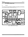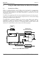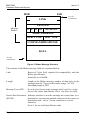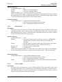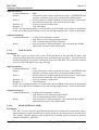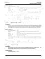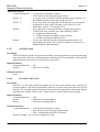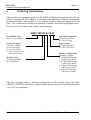
1
Quin Systems Limited BMC302B Hardware Reference Manual MAN 610 Issue 1.0 February 1997 Copyright Notice Copyright 1997 Quin Systems Limited. All rights reserved. Reproduction of this document, in part or whole, by any means, without the prior written consent of Quin Systems Limited is strictly prohibited. Important Notice Quin Systems reserves the right to make changes in the products described in this document in order to improve design or performance and for further product development. Examples given are for illustration only, and no responsibility is assumed for their suitability in particular applications. Reproduction of any part hereof without the prior written consent of Quin Systems is prohibited. Although every attempt has been made to ensure the accuracy of the information in this document, Quin Systems assumes no liability for inadvertent errors. Suggestions for improvements in either the products or the documentation are welcome. European Community Directives This product has not been tested to the protection requirements of the EMC Directive (89/336/EEC) as amended by Directives 92/31/EEC and 93/68/EEC. It is therefore the responsibility of the system integrater to ensure that the overall system complies with the requirements of these Directives. If this poduct is to be incorporated into a system for the control of machinery: • it must not be relied upon to provide safety-critical features such as guarding or emergency stop functions. • it must not be put into service until the machinery into which it has been incorporated has been declared in conformance with the Machinery Directive (89/392/EEC) as amended by Directives 91/368/EEC, 93/44/EEC and 93/68/EEC. This product, as normally supplied, has low voltages accessible to touch and must be mounted within a suitable cabinet to meet any required IP rating to BS EN 60529.The installation instructions in this manual should be followed in constructing a system which complies with all relevant Directives. Issue 1.0 BMC302B Hardware Reference Manual Versions This manual reflects the following versions of hardware and software: • Microsoft Windows 3.0 and above • Microsoft Visual Basic version 1 and above • Wonderware Intouch version 3 and above • Quin qDCX302 version 1.1 and above • Microtech Research MCC68K ‘C’ Compiler • Microtech Research Xray 68K Debugger • BMC302 Hardware Issue B Quin Systems Ltd. Oaklands Business Centre, Oaklands Park, Wokingham, Berkshire. RG41 2FD National Tel: National Fax: email: Compuserve: 01734 - 771077 01734 - 776728 [email protected] 100572,1631 International Tel: +44-1734-771077 International Fax: +44-1734-776728 Quin is a trademark of Quin Systems Ltd. Intel and iDCM44 are trademarks of Intel Corp. Microsoft, Windows and Visual Basic are trademarks of Microsoft Corp. Intouch is a trademark of Wonderware Inc. Copyright © 1997 Quin Systems Limited Page iii BMC302B Hardware Reference Manual ISSUE Issue 1.0 DATE REVISION HISTORY 0.1 Draft Copy IDH Jan 1997 1.0 First Issue IDH Feb 1997 Page iv Copyright © 1997 Quin Systems Limited Issue 1.0 BMC302B Hardware Reference Manual Contents 1. Introduction 1.1 General 1.2 Rated Performance 1.3 Physical Dimensions 1.4 Power Supply Requirements 1.5 Environmental Specification 1.6 Conformity to EC Directives 5 6 8 8 8 9 9 2. Description of Operation 2.1 General 2.2 Bitbus Interface 2.3 XBus2+ Expansion Bus 2.4 Optional RS232/RS485 Ports 2.5 Serial EEPROM 2.6 Hardware Watch-Dog 2.7 Diagnostic LEDs 10 10 11 12 12 12 13 13 3. Using the BMC302B Within the Bitbus Environment 3.1 Introduction to Bitbus 3.1.1 Physical Characteristics 3.1.2 Modes of Operation 3.1.3 Data Link Protocol 3.1.4 Message Specification 3.1.5 Remote Access and Control (RAC) Commands 3.2 qDCX302 Remote Access and Control (RAC) Task Summary19 3.3 Quin Bitbus Libraries 3.4 BMC302B Memory Model 3.5 Remote Access and Control (RAC) Command Reference 3.5.1 RESET STATION (00H) 3.5.2 CREATE TASK (01H) 3.5.3 DELETE TASK (02H) 3.5.4 GET FUNCTION ID (03H) 3.5.5 RAC_PROTECT (04H) 3.5.6 READ IO (05H) 3.5.7 WRITE IO (06H) 3.5.8 UPDATE IO (07H) 3.5.9 UPLOAD MEMORY (08H) 3.5.10 DOWNLOAD MEMORY (09H) 3.5.11 OR IO (0AH) 3.5.12 AND IO (0BH) 3.5.13 XOR IO (0CH) 3.5.14 READ INTERNAL (0DH) 14 14 15 15 15 15 18 Copyright © 1997 Quin Systems Limited 19 20 21 21 21 22 22 22 23 23 23 24 24 25 25 26 26 Page 1 BMc302B Hardware Reference Manual 3.5.15 3.5.16 3.5.17 3.5.18 3.5.19 Issue 1.0 WRITE INTERNAL (0EH) NODE INFO (0FH) OFFLINE (10H) UPLOAD CODE (11H) DOWNLOAD CODE (12H) 27 27 28 28 29 4. Hardware Configuration 4.1 Introduction 4.2 Module Reset J1 4.3 ROM Type Selector J2 4.4 SRAM Size Selector J3 4.5 Bitbus Mode Register J4 4.6 Bitbus Terminators J5 4.7 Serial Port B RTS Source Selector J6 4.8 Module Address Configuration SW1, SW2 4.9 MC68302 Configuration Details 30 30 31 32 32 33 34 34 35 36 5. Connections 5.1 General 5.2 Signal Names 5.3 Power Supply Connector T1 5.4 Bitbus Connections 5.5 Serial Port Connections 5.6 XBus Expansion Connector Details. P2 38 38 38 38 39 39 40 6. Ordering Information 42 Page 2 Copyright © 1997 Quin Systems Limited Issue 1.0 BMC302B Hardware Reference Manual List of Figures Figure 1. BMC302SB:Block Diagram 11 Figure 2. Typical BMC302 Installation 15 Figure 3. Bitbus Message Structure 17 Figure 4. : Memory Model for BMC302 Running qDCX302 V1.0 21 Figure 5. BMC302B and BMC302SB Power and Jumper Locations 31 Figure 6. Module Reset Selector J1 32 Figure 7. EPROM Selector J2 33 Figure 8. SRAM Selector J3 34 Figure 9. Bitbus Mode Register J4 34 Figure 10. Bitbus Termination Selector J5 35 Figure 11. Serial Port B RTS Source Selector J6 36 Figure 12. Node Address Selector Switches SW1 & SW2 36 Figure 13. Power Connector Placement 39 Figure 14. Bitbus D-Type Connector Details 40 Figure 15. High Speed Serial Port D-Type Connector Details 41 Figure 16. BMC302 Issue B: XBus2+ Expansion Bus connections 42 Copyright © 1997 Quin Systems Limited Page 3 BMC302B Hardware Reference Manual Page 4 Issue 1.0 Copyright © 1997 Quin Systems Limited Issue 1.0 1. BMC302B Hardware Reference Manual Introduction This manual describes the operation and capabilities of the Quin Systems Bitbus Carrier module. This module is available in two formats: BMC302B: This module interfaces to the Bitbus network and provides an XBus2+ expansion bus interface for use with Quin Bitbus expansion modules. BMC302SB: In addition to the XBus2+ interface provided by the BMC302B, this module also provides 2, galvanically isolated, software configurable serial communications ports. The part number BMC302B will be used throughout this manual to describe the generic part and all information provided within this manual refers to the generic module unless specifically stated otherwise. External References: 001 qDCX302 Distributed Control Executive Software Manual for the dDCX302 Bitbus Operating System Issue 1.0 Part number MAN611 002 The Bitbus Interconnect Serial Control Bus Specification Part Number 280645-001, Intel Corporation Release 001 Rev B 7/88 003 Bitbus DDE manual for Windows 3.1 Quin Systems Ltd. 004 Bitbus DLL manual for Windows 3.1 Quin Systems Ltd. 005 Motorola MC68302 User’s Manual Rev. 2 Motorola Copyright © 1997 Quin Systems Limited Page 5 BMC302B Hardware Reference Manual 1.1 Issue 1.0 General The BMC302B is a compact DIN rail mounted Bitbus module which provides the user a fully configured interface between the Bitbus high-speed serial network and the XBus2+ parallel expansion bus. The BMC302B module is based on the Motorola MC68302 microcontroller with 128K/512K RAM and 256K/512K EPROM or 512K Flash EPROM which form a complete microcomputer system. This system runs the qDCX302 real-time, multi-tasking operating system which is a compatible superset of the Intel iDCX51 operating system. Each BMC302B has a preprogrammed Remote Access and Control (RAC) task which provides all of the RAC functionality as required by the Bitbus Interconnect specification and thereby ensures that the BMC302B is fully compatible with other manufacturer’s Bitbus products. The BMC302B is designed for operation in the industrial environment. It complies with all relevant EU EMC Directives and utilises galvanic isolation to ensure a high degree of noise immunity from the local environment. The electrical interface to Bitbus conforms to the RS485 standard and is in addition galvanically isolated from the remainder of the module. The unit also possesses watch-dog circuitry which will invoke a full hardware reset should the Watch-Dog task fail to toggle the input once every 1.5 seconds. This watch-dog facility may be enabled or disabled by a jumper link. The RAC task enables the BMC302B to be fully applied from PC resident programs which utilise a Bitbus compliant driver program. The use of the Quin BBPCMS or IBC-PC-CON master card together, with the Quin Bitbus libraries, enables rapid system development using standard PC development tools and languages. A second, Watch-Dog, task is also provided which continuously monitors the operation of the module and will cause a hardware reset should the module cease functioning. The module is also designed to facilitate the programming and execution of custom firmware which can be programmed into EPROM or downloaded via Bitbus and programmed into the optional Flash EPROM. In this way the operation and general functionality of the module can be changed on network initialisation or during operation. All module resident firmware comprises tasks running under qDCX302. These on-module tasks can perform local control and data acquisition functions which are capable of maintaining control in the event of a network failure. The reader is referred to the qDCX302 Bitbus Operating System manual (MAN611) for further information on the development of qDCX302 tasks. Page 6 Copyright © 1997 Quin Systems Limited Issue 1.0 BMC302B Hardware Reference Manual On the BMC302SB one further task, Serial Driver, is provided which controls the operation of the two high speed bidirectional serial ports. This task handles all lowlevel control of the ports and provides a high-level user-interface which facilitates simple configuration of protocols, handshaking etc. and even configuration for RS232 (point to point) or RS485 (multidrop) networks. The reader is referred to the BMC302SB Serial Driver Programmers Manual (MAN612) for further details. Some Quin expansion modules, eg. the BMAIX16 analogue input module, require special driver tasks to control their operation. These drivers are provided by Quin preprogrammed into EPROM or as dowloadable modules for storing in Flash EPROM on the BMC302B. The XBus2+ expansion bus permits the user to connect a selection of up to five of the large range of Quin Bitbus expansion modules. It also facilitates the interfacing of custom modules to the Bitbus network with full technical support available from Quin Systems. The BMC302SB may be used either as a Bitbus master or slave node. Throughout the remainder of this manual it is assumed that it is being used as a slave device, for further information on using the BMC302SB module as a master Bitbus device the reader is referred to the BMC302SB Serial Gateway Reference Manual (MAN613). Copyright © 1997 Quin Systems Limited Page 7 BMC302B Hardware Reference Manual 1.2 Issue 1.0 Rated Performance This section details the rated performance of the BMC302B and BMC302SB modules. Table 1: BMC302B and BMC302SB Rated Performance Bitbus Mode Max. Baud Rate RS232/485 Ports Max. Baud Rate Synchronous 1.67 Mbaud 2 38.4 kbaud Asyncronous 375 kbaud 2 38.4 kbaud Asynchronous 62.5 kbaud 2 38.4 kbaud The BMC302B and BMC302SB modules are designed to maintain their rated performance without the need for any user adjustments. This is achieved through the use of high precision, high stability components. 1.3 Physical Dimensions The standard module is provided with D-Type connectors for all serial communications links. A two-part two-pin combicon connector is provided for application of the 24Vdc power supply. This facilitates pre-wiring of harnesses etc. prior to installation of the module. The table below shows the space required for installation. Length 225mm Width 77mm (raft base only) Height 40mm (from top of DIN rail) Weight 0.4 kg Table 2: Module Dimensions 1.4 Power Supply Requirements The power supply for the module is derived from the main 24Vdc supply via a 10W dc/dc converter which provides galvanic isolation of the 24V and regulation down to 5Vdc. The BMC302B only requires 50% of the converter’s output capacity, this leaves a total of 5W for powering expansion modules connected to the XBus2+ connector. Page 8 Copyright © 1997 Quin Systems Limited Issue 1.0 1.5 BMC302B Hardware Reference Manual Environmental Specification The table below shows the operating and storage environmental limits: Temperature Ranges Rated Performance 0 -50 C Storage -25 C - 70C Rel Humidity 0 to 95% at 50 C Table 3: Temperature Ranges If necessary, the unit can be supplied in a suitable sealed cabinet. Please contact your sales office or Quin Systems directly for further details. 1.6 Conformity to EC Directives If this product is incorporated into system for the control of machinery, it must not be relied upon to provide safety-critical features such as guarding or emergency stop functions. It must not be put into service until the machinery into which it has been incorporated has been declared in conformity with the Machinery Directive 89/392/ EEC and/or its relevant amendments. These installation instructions should be followed in constructing a system which meets requirements. This product has not been tested to the protection requirements of the EMC Directive (89/336/EEC) as amended by Directives 92/31/EEC and 93/68/EEC. It is therefore the responsibility of the system integrator to ensure that the overall system complies with the requirements of these Directives. This product only uses low voltages, and is therefore exempt under the Low Voltage Directive (73/23/EEC) as amended by 93/68/EEC. The product as normally supplied has low voltages accessible to touch, and must be mounted within a suitable cabinet to meet any required IP rating to BS EN 60529. Copyright © 1997 Quin Systems Limited Page 9 BMC302B Hardware Reference Manual Issue 1.0 2. Description of Operation 2.1 General This section summarises the operation of the Bitbus Carrier module. The following is a block diagram of the BMC302SB, the BMC302B is similar but does not have the circuitry associated with the two RS232/485 serial ports. EPROM/ FLASH RAM Diagnostic LEDs XBus2+ Data & Address Buffers Serial EEPROM MC68302 MicroController Bitbus RS485 Serial Port 1 Address Data & Control Serial Ports 2&3 OptoIsolators Watch-dog Mode Register XBus 2+ 5A Node Address Hardware Selector Reset Main 24V to 5V DC/DC Power Supply Port A Buffers RS232 / RS485 Port B Buffers RS232 / RS485 DC/DC OptoIsolators DC/DC Figure 1. BMC302SB:Block Diagram Page 10 Copyright © 1997 Quin Systems Limited Issue 1.0 BMC302B Hardware Reference Manual The BMC302B is based on the Motorola MC68302 integrated multiprotocol processor (IMP). The IMP has the benefit of a closely coupled, industry-standard, M68000 microprocessor core, a system integration block (SIB) and a dedicated communications processor (CP). This configuration makes the 68302 ideally suited to the BMC302B application as it has three high speed serial ports each of which can be software configured to run many different protocols. This device together with the 128k/512k bytes of RAM and 256k/512k bytes of ROM form a powerful target processor system capable of high speed processing of quite complex programs. The standard BMC302B is preprogrammed to run the qDCX302 real-time, multi-tasking operating system. The BMC302B is provided with a set of five diagnostic LEDs which are driven directly by the processor and indicate, the state of the system during powerup tests, the state of the Bitbus Data and RTS lines, and the state of the hardware watchdog. The Bitbus network is buffered by RS485 tranceivers, optically isolated and then fed into the MC68302, serial port 1. The associated Tx and Rx control lines and data synchronisation are handled by a PZ5032 CPLD (Complex Programmable Logic Device). The two optional serial ports, Port A and Port B, are also buffered, by software configurable LTC1334 RS232/485 transceivers, and then optically isolated before being fed into the MC68302 serial ports 2 and 3 respectively. The parallel data and address buses of the MC68302 are decoded by a second PZ5032 CPLD to produce the required control signals to drive the XBus2+ multiplexed 12 bit address/8 bit data bus. The addition of Mode Register and Node Address selectors enables the BMC302B to initialise in the correct Bitbus communication mode. These devices are read by the processor during initialisation of the qDCX302 operating system to determine the Bitbus baud rate and the Node address of the module on the Bitbus network. 2.2 Bitbus Interface The BMC302B interfaces to the IEEE1118 industry standard Bitbus interconnect as a slave node. Bitbus is based on a high speed RS485 multidrop network which has one master node and up to 250 slave nodes. On initial application of power, or following a reset, the qDCX302 operating system reads the Mode Register and Node Address switches to determine the speed and mode (synchronous/asynchronous) of the Bitbus network to which the module is connected. It is therefore essential that both the Mode Register and Node Address switches are set up before power is applied to the module. Note: All nodes on the same network must have a unique node number (00...FA) and all nodes must be configured to use the same communication speed and mode. Copyright © 1997 Quin Systems Limited Page 11 BMC302B Hardware Reference Manual 2.3 Issue 1.0 XBus2+ Expansion Bus The XBus2+ expansion bus is decoded from the MC68302 address and data bus to provide a simple but flexible multiplexed 12 bit address / 8 bit data bus. The bus is buffered by three 74BCT245 transceivers with additional 100 ohm series termination of the high speed /RD, /WR, /SEL, /ALE and /EXP signals. In addition to the address and data lines the XBus2+ also has two dedicated interrupt lines INT0 & INT1 which are connected to the Ext.0 (PB8) and Ext.1 (PB9) interrupt inputs of the MC68302. Four power supply lines (two 0V and two +5V) are also provided to enable low-power expansion modules to be supplied directly from the expansion bus. XBus2+ is a 34 way compatible superset of the 26 way XBus2 expansion bus. The first 26 pins of the XBus2+ connector have identical functionality to the XBus2 making it simple to interface to all existing XBus2 expansion modules. For further details about interfacing to the XBus2+ expansion bus the reader is referred to the ‘Interfacing to the XBus2+ Expansion Bus’ manual (MAN614) available from Quin Systems. NOTE: The maximum current that can be drawn from the +5V XBus2+ supply is 1.0 Amp. Under no circumstances must the XBus2+ load be permitted to exceed this level as erratic operation of the BMC302B may result. 2.4 Optional RS232/RS485 Ports The BMC302SB has two additional high-speed serial communication ports (Port A and Port B). Each port is driven directly from one of the MC68302 serial ports (2 or 3), through LTC1334 transceivers. These devices can be independently configured, via software, to provide RS232 or RS485 compatible drive voltages. The serial communication protocol and handshaking, used by the MC68302, are also software configurable thus enabling a wide variety of serial communication links to be interfaced. Each port is galvanically isolated from the remainder of the BMC302B by the use of opto-isolators and DC/DC converters. In normal use the serial ports A and B are accessed via Bitbus messages to the moduleresident Serial Driver task. This task handles all of the data buffering and hardware/ software handshaking which is normally associated with serial communications. For further information on use of the serial ports the reader is referred to the BMC302SB Serial Driver Reference Manual (MAN612). 2.5 Serial EEPROM A non-volatile 512 * 8 bit X25040 serial EEPROM is provided for saving module configuration information. This device is accessed via special functions provided within the RAC interface. Page 12 Copyright © 1997 Quin Systems Limited Issue 1.0 2.6 BMC302B Hardware Reference Manual Hardware Watch-Dog To ensure continuous operation of the BMC302B a MAX705 hardware watch-dog I.C. is provided. When the watch-dog is enabled the MAX705 WDI input must be toggled, by the MC68302 processor, once every second. Each BMC302B has a pre-defined WDOG task, resident in ROM, which is automatically invoked during module initialisation. This task monitors the state of all active qDCX302 tasks together with the state of the BMC302B power supply. Once enabled, the expiry of the WDOG timeout instigates a full reset of the BMC302B hardware. 2.7 Diagnostic LEDs To facilitate diagnosis of system faults the BMC302B is provided with five diagnostic LEDs (L1...L5). The operation of these LEDs is discussed below: L1 & L2 These two LEDs (L1 red, L2 green) are used during system initialisation to indicate the state of various system components as shown in the following table Table 4: State L1 Red L2 Green Initialising On On Boot Sequence Complete Initialising qDCX302 Off Off qDCX302 Installed and Running Off On Once the module has booted these LEDs are available for use by custom applications. L3 & L4 This yellow LED is illuminated while the module is transmitting Bitbus messages. L4 This yellow LED is illuminated when the Bitbus DATA line is a logic ‘1’. L5 The red WDOG LED indicates the state of the WDI input to the MAX705. It is illuminated when the WDI input is a logic ‘0’. When the watch-dog is enabled the WDI input must be toggled every 1.6 seconds to prevent a hardware reset. Consequently this LED normally flashes with a period of approximately 1 second. Copyright © 1997 Quin Systems Limited Page 13 BMC302B Hardware Reference Manual Issue 1.0 3. Using the BMC302B Within the Bitbus Environment 3.1 Introduction to Bitbus Bitbus is a high performance, serial Fieldbus network designed for communication between distributed process I/O and intelligent controllers. It uses the IEEE-1118 international open standard for the Bitbus Interconnect as specified by the Intel Corporation in 1984. The IEEE1118 standard specifies the electrical and data link protocols for the network, along with the application message structure and protocol for use with a multi-tasking operating environment such as qDCX302. The BMC302B is primarily intended to be used as a slave Bitbus node which is connected to a number of expansion modules via the XBus2+ expansion bus. The BMC302B would typically form part of a distributed Bitbus network which would include a PC resident Master card as shown in the following figure: PC Bitbus Temperature Monitor/Controllers 88.5 °C RS232 Set BMC302SB Bitbus Boiler Vessel BMC302SB BMDX1616B RS485 20.4 °C Set Figure 2. Typical BMC302B Installation Page 14 Copyright © 1997 Quin Systems Limited Issue 1.0 3.1.1 BMC302B Hardware Reference Manual Physical Characteristics The network uses a simple multi-drop bus configuration, with the standard RS-485 (twisted pair) specification cable link. This standard has been thoroughly tested and proven for industrial communications and is currently in world-wide use. 3.1.2 Modes of Operation Bitbus supports two modes of operation, synchronous for very high speed performance and asynchronous (or self-clocked) for operation over large distances. Synchronous mode of operation allows Bitbus to operate at speeds of 500kbits/sec or 2.4Mbits/sec, with a maximum of 28 nodes distributed over a physical distance of 30 metres. Self-clocked operation allows Bitbus to be used for much larger distances, with the ability to link together up to 250 nodes over a distance of up to 13.2km. In this mode Bitbus can use multiple segments, linked via repeaters, to achieve a range of 13.2 km at 62.5kbits/sec or 3.3 km at 375kbits/sec. 3.1.3 Data Link Protocol Bitbus uses a highly reliable Master-Slave protocol. This uses a single master node to control all communication on the network. Each message transaction is initiated by the master node by sending an order to a specified slave, then polling for a reply. Slaves only send messages on the network in response to an order from the master. 3.1.4 Message Specification The Bitbus protocol uses a similar structure for both order and reply messages. The master starts a transaction by issuing an order to a slave. The slave must then respond with a reply back to the master. The application message structure is the same for all Bitbus communications and is shown in the following figure: Copyright © 1997 Quin Systems Limited Page 15 BMC302B Hardware Reference Manual Issue 1.0 MSB LSB LINK first bit transmitted LENGTH Message Header MT SE DE TR RESERVED NODE ADDRESS SOURCE TASK DEST. TASK COMMAND/RESPONSE DATA last bit transmitted Figure 3. Bitbus Message Structure The contents of the Bitbus message fields are explained below: Link: Reserved 2 byte field, required for compatibility with the Bitbus specification. Normally set to 0000H. Length: Length of the Bitbus message, number of data bytes in the message plus the 7 bytes in the header (range 7 to 255). Maximum length is FFH Message Type (MT): Set to 0 (zero) for an order message and 1 (one) for a reply. Set to 0 for orders from Master. Set to 1 by Slave on reply. Source/Dest Extension: Indicates whether or not the message has come from, or is (SE/DE) destined for, an extension module connected to the source or destination node. Set to 1 for an extension or 0 (zero) otherwise. Set to 1 for use with Quin Master cards. Page 16 Copyright © 1997 Quin Systems Limited Issue 1.0 BMC302B Hardware Reference Manual Track (TR): Used by some implementations for message control. If used it is set to 0 (zero) on sending and 1 on receiving. Set to 0 for use with Quin Master cards. Reserved: Reserved for possible future enhancements. Cleared on send, unknown on receive. Set to 0 for use with Quin Master cards. Node Address: Destination node for orders, source node for replies, i.e. it doesn’t change during the message transaction. In the range 1-250. Set to zero for intertask messages on BMC302B. Set to 01H...FAH to access slave nodes on network or set to FFH to access a Quin master card from a PC resident task. Source Task: The task that initiated the message transaction or that will receive the reply (depending on the value set in the Message Type field). Set to 1 for use with Quin Master cards. Destination Task: The task that will receive the original order message or the source of the reply message. Set to 0 to access RAC functions or 1..7 to access other module-resident tasks. Command / Response: This field is normally used by user tasks to identify the message within the overall user application, i.e. read, write, update command message. It is also used by the Bitbus message protocol in message responses to indicate errors that have occurred. See following section for detailed information on the contents of this field. Data: The Data field contains any data specific to the Bitbus message and is defined by the command field. This field is the only optional field in the message and can be in the range from 0 bytes to 248 bytes long, dependent on implementation. The Bitbus specification requires that every Bitbus node be able to accept a message length of 20 bytes, ie. 13 bytes of data, however, the maximum permitted message length is 255 bytes giving a maximum data field size of 248 bytes. See following section for detailed information on the contents of this field. Copyright © 1997 Quin Systems Limited Page 17 BMC302B Hardware Reference Manual 3.1.5 Issue 1.0 Remote Access and Control (RAC) Commands The Bitbus specification defines a set of high level commands (and associated responses) to carry out various general purpose operations on remote slave nodes. This interface, the Remote Access and Control (RAC) command interface, provides a standard means of interrogating slave nodes across all Bitbus network implementations. The remote access interface provides the user with general I/O read & write facilities, together with memory upload and download capability. The remote control functions allow control and monitoring of tasks at remote slaves. When supported, the RAC interface is always implemented as task 0 (zero) on the slave node and makes use of the standard Bitbus message protocol. This enables RAC commands to be implemented as standard on all Bitbus nodes. The functions specified and supported by RAC are shown in the following table: Table 5: Bitbus RAC Commands Control Command /Response Reset * 00H Perform software reset Create Task * 01H Start a module-resident task Delete Task * 02H Delete a module-resident task Get Function IDs * 03H Return IDs of all running tasks RAC Protect * 04H Suspend/Resume Access services Command Access Action Taken by Task 0 Read I/O * 05H Return data from specified I/O ports Write I/O * 06H Write to specified I/O ports Update I/O * 07H Update specified I/O ports Upload Memory * 08H Return values from specified memory area Download Memory * 09H Write values to specified memory area. OR I/O * 0AH OR values into specified I/O ports AND I/O * 0BH AND values into specified I/O ports XOR I/O * 0CH XOR values into specified I/O ports Read Internal * 0DH Read values from specified ‘internal’ memory Write Internal * 0EH Write values to specified ‘internal’ memory Node Information * 0FH Return module related information. 10H Set remote node offline Offline * Upload Code * 11H Read values from code memory space Download Code * 12H Write values to specified code space Page 18 Copyright © 1997 Quin Systems Limited Issue 1.0 3.2 BMC302B Hardware Reference Manual qDCX302 Remote Access and Control (RAC) Task Summary The Remote Access and Control (RAC) service, contained in task 0, allows resources on Bitbus nodes interconnected via a Bitbus network, to be accessed via the standard Bitbus message interface. The qDCX302 RAC task provides exactly the same functionality as the iDCX RAC commands contained within task 0 included on the 8044BEM processor. A RAC service request is made by sending an order message to task 0 on the node at which the service is to be performed. RAC order messages are standard Bitbus messages that have the COMMAND/RESPONSE field set to indicate which RAC service is to be performed. Any additional required information is sent and received in the DATA field. 3.3 Quin Bitbus Libraries The simplest way of utilising the BMC302B on a Bitbus network is to connect the network to a PC resident master card. If this master card is compatible with the Intel standard, eg the Quin BBPCMS or IBC-PC-CON master card, the network can be controlled using the high-level functions provided within the Quin Bitbus Libraries. These functions support all of the standard RAC commands together with the extended RAC facilities available under qDCX302. Use of the Quin libraries relieves the programmer of most of the protocol and error handling thus ensuring maximum productivity and a robust system design. A user-friendly monitor program is available which allows the system designer to manually exercise the RAC functions on the BMC302B and all other makes of Bitbus node. Copyright © 1997 Quin Systems Limited Page 19 BMC302B Hardware Reference Manual 3.4 Issue 1.0 BMC302B Memory Model All of the peripheral devices including the XBus2+ expansion bus are memory mapped utilising the address decoding and chip select functions provided within the MC68302. The resultant module memory map is shown in the following figure: FFFFFF FFFFFE FFDFFF Internal I/O Standard External I/O @ 1MHz FFD000 FFCFFF Fast External I/O @ 2MHz FFC000 81FFFF 81007F 810000 80FF00 User Memory Application Task Static Variables User Application Task Descriptors System Variables Memory Mapped I/O Accessed using RAC task Read & Write I/O, Update I/O, OR I/O, AND I/O XOR I/O RAM 128K (optional 512K) Accessed using RAC task Download Memory &Upload Memory System Heap task stacks system message pool qDCX302 stack Jump Table 800000 700FFF 700000 MC68302 Registers MC68302 Registers & dual-port RAM User Application Task Code EPROM 256K (optional 512K) or FLASH 512K 03FFFF 010000 00FFFF Unused qDCX302 RAC Task Accessed using RAC task Download Code &Upload Code qDCX302 Operating System Vector Table 000000 Figure 4. Memory Model for BMC302B Running qDCX302 V1.0 Page 20 Copyright © 1997 Quin Systems Limited Issue 1.0 3.5 BMC302B Hardware Reference Manual Remote Access and Control (RAC) Command Reference This section explains the functions performed by each of the qDCX302 standard RAC commands which are identical to those in the Intel iDCM-44 operating system. All memory mapping required to translate I/O and memory locations to the MC68302 memory map (figure 4) are carried out within the RAC application and are transparent to the user. 3.5.1 RESET STATION (00H) Description This RAC service performs a software reset (causes jump to restart vector) on the node at the specified address. No reply is returned, unless there is a general error with the operation. NOTE: An Offline command should be issued following a Reset Station to ensure that the Master resynchronises with the reset slave node. Input Parameters Command/Response = 00H Output Parameters None. If the operation was carried out successfully. Command/Response = 91H. If node didn’t exist. 3.5.2 CREATE TASK (01H) Description This RAC service creates (runs) the task whose Initial Task Descriptor (ITD) resides at the address given in the DATA field. Status is returned in the reply message Command/Response field. Input Parameters Command/Response = 01H Data(0) = high byte ITD address offset Data(1) = low byte ITD address offset Output Parameters Command/Response = valid response from create task system call, or = 81H-86H If create task failed. = 91H Protocol error during message transfer NB: The ITD address offset is handled by the RAC using the following procedure: RAC first looks for an ITD pattern (indicating the start of an ITD) in external RAM memory (using an external memory offset value). If one isn’t found, it automatically checks in code memory for the ITD (using a code memory offset value). An error is only reported if no ITD is found in either memory area. This technique facilitates debugging by enabling code to be downloaded directly to RAM to effectively "overwrite" a task already stored in EPROM. Copyright © 1997 Quin Systems Limited Page 21 BMC302B Hardware Reference Manual 3.5.3 Issue 1.0 DELETE TASK (02H) Description This RAC service deletes (kills) a running task which has the task ID given in the Data field. Status is returned in the reply message Command/Response field. Input Parameters Command/Response = 02H Data(0) = task ID (0..7) Output Parameters Command/Response = 0 The task was successfully deleted = 80H the specified task did not exist = 91H Protocol error during message transfer 3.5.4 GET FUNCTION ID (03H) Description This RAC service returns the Function IDs for all currently running tasks. The FID table is returned in the reply message Data field. Input Parameters Command/Response = 03H Data (0 to 7) = An 8 byte array to allow buffer space for reply. The data values contained in the array are of no consequence. Output Parameters Command/Response = 0 Successful command execution = 91H Protocol error during message transfer Data (0 to 7) = FID table for currently running tasks. Any unused element is set to 0 by this RAC service. 3.5.5 RAC_PROTECT (04H) Description This RAC service disables or enables certain RAC services. If a disable RAC Protect message is sent, further RAC services at this node are suspended until a re-enable RAC Protect message is sent. If an attempt is made to invoke a disabled RAC service a value of 95H is returned in the Command/Response indicating that it is currently RAC protected. Input Parameters Command/Response = 04H Data(0) = 0 to disable RAC services or = 1 to re-enable RAC services Output Parameters Command/Response = 0 Successful command execution = 91H Protocol error during message transfer Page 22 Copyright © 1997 Quin Systems Limited Issue 1.0 3.5.6 BMC302B Hardware Reference Manual READ IO (05H) Description This RAC service reads the specified I/O ports and returns their values. I/O port references and returned I/O bytes are stored in a structured array in the Data field. Input Parameters Command/Response = 05H Data(0) = a byte offset value, relative to the base I/O space = 00FFDF00H, that provides a reference to the I/O location to be read. Data(1) = an 8-bit place holder where the returned I/O byte will be placed. Data (len - 8) = Last I/O reference in Data field. Data (len - 7) = Last data byte placeholder. NOTE: The maximum number of I/O ports that can be read at one request is determined by the size of the data field which is set by the message length less the 7 bytes for the header. Output Parameters Command/Response = = = Data() = 3.5.7 0 Successful command execution 91H Protocol error during message transfer 95H Command presently RAC protected same as shown in "Input Parameters" above but with the read I/O data contained in the relevant 8-bit databyte place holder. WRITE IO (06H) Description This RAC service writes to the specified I/O ports. I/O port reference and write byte are stored in a structured array in the Data field. Input Parameters Command/Response = 06H Data(0) = a byte offset value, relative to the base I/O space = 00FFDF00H, that provides a reference to the I/O location to be written. Data(1) = an 8-bit value to be written to the preceding I/O port. Data(len - 8) = Last I/O reference in Data field. Data(len - 7) = Last byte to be written. NOTE: The maximum number of I/O ports that can be written at one request is determined by the size of the data field which is set by the message length less the 7 bytes for the header. Output Parameters Command/Response = 0 Successful command execution = 91H Protocol error during message transfer = 95H Command presently RAC protected 3.5.8 UPDATE IO (07H) Description This RAC service writes to the specified I/O ports and then rereads and returns the read values. I/O port reference and write byte are stored in a structured array in the Data field. The read I/O byte is returned in place of the write byte in the reply message. Copyright © 1997 Quin Systems Limited Page 23 BMC302B Hardware Reference Manual Issue 1.0 Input Parameters Command/Response = 07H Data(0) = a byte offset value, relative to the base I/O space = 00FFDF00H, that provides a reference to the I/O location to be read/written. Data(1) = an 8-bit value to be written to the preceding I/O port. Upon return, this field will contain the value read from the I/O port. Data(len - 8) = Last I/O reference in data field. Data(len - 7) = Last byte to be written. NOTE: The maximum number of I/O ports that can be updated at one request is determined by the size of the data field which is set by the message length less the 7 bytes for the header. Output Parameters Command/Response = = = Data() = 3.5.9 0 Successful command execution 91H Protocol error during message transfer 95H Command presently RAC protected same as shown in "Input Parameters" above but with the write bytes replaced by the returned I/O bytes. UPLOAD MEMORY (08H) Description This RAC service reads a specified number of bytes from external memory starting at a specified address. qDCX302 automatically adds any required offset from the base of external memory. The message length field minus 9 bytes for the message header and starting address determines the number of bytes read. Values read are returned in the reply message. Input Parameters Command/Response = 08H Data(0) = High byte of starting address. Data(1) = Low byte of starting address. Output Parameters Command/Response = 0 Successful command execution = 91H Protocol error during message transfer = 95H Command presently RAC protected Data(2 to (length - 9))= An array of data bytes read. The number of bytes returned depends upon the message length specified minus 9 bytes for the message header and starting address. NOTE: The maximum number of memory locations that can be uploaded at one request is determined by the size of the available data field which is set by the message length less the 7 bytes for the header and the 2 bytes for the starting address. 3.5.10 DOWNLOAD MEMORY (09H) Description This RAC service writes a specified number of bytes to external memory starting at a specified address. qDCX302 automatically adds any required offset from the base of external memory. The value of message length minus 9 bytes for the message header and starting address determines the maximum number of bytes that can be downloaded. Page 24 Copyright © 1997 Quin Systems Limited Issue 1.0 BMC302B Hardware Reference Manual Input Parameters Command/Response = 09H Data(0) = High byte of starting address. Data(1) = Low byte of starting address. Data(2 to (length - 9))= An array of data bytes to be written. NOTE: The maximum number of memory locations that can be downloaded at one request is determined by the size of the available data field which is set by the message length less the 7 bytes for the header and the 2 bytes for the starting address. Output Parameters Command/Response = 0 Successful command execution = 91H Protocol error during message transfer = 95H Command presently RAC protected 3.5.11 OR IO (0AH) Description This RAC service performs one or more OR operations on the specified I/O ports, with specified OR masks, then rereads the ports, and returns the values read. I/O port reference and OR mask byte are stored in a structured array in the Data field. The byte read is returned in place of the OR mask in the reply message. Input Parameters Command/Response = 0AH Data(0) = a byte offset value, relative to the base I/O space = 00FFDF00H, that provides a reference to the location to perform the OR operation. Data(1) = an 8-bit value to be ORed with the specified I/O port. Upon return, this field will contain the value read from the I/O port. Data(len - 8) = Last I/O reference in Data field. Data(len- 7) = Last OR mask. NOTE: The maximum number of I/O ports that can be ORed at one request is determined by the size of the data field which is set by the message length less the 7 bytes for the header. Output Parameters Command/Response = 0 Successful command execution = 91H Protocol error during message transfer = 95H Command presently RAC protected Data() = same as "Input Parameters" above but with the ORed data returned in place of the OR masks. 3.5.12 AND IO (0BH) Description This RAC service performs one or more AND operations on the specified I/O ports, with specified AND masks, then rereads the ports, and returns the read values. I/O port reference and AND mask byte are stored in a structured array in the Data field. Read byte is returned in place of the AND mask in the reply message. Copyright © 1997 Quin Systems Limited Page 25 BMC302B Hardware Reference Manual Issue 1.0 Input Parameters Command/Response = 0BH Data(0) = a byte offset value, relative to the base I/O space = 00FFDF00H, that provides a reference to the I/O to perform the AND operation. Data(1) = an 8-bit value to be ANDed with the specified I/O port. Upon return, this field will contain the value read from the I/O port. Data(len - 8) = Last I/O reference in Data field. Data(len - 7) = Last AND mask. NOTE: The maximum number of I/O ports that can be ANDed at one request is determined by the size of the data field which is set by the message length less the 7 bytes for the header. Output Parameters Command/Response = = = Data() = 3.5.13 0 Successful command execution 91H Protocol error during message transfer 95H Command presently RAC protected same as shown in "Input Parameters" above but with the ANDed data returned in place of the AND masks. XOR IO (0CH) Description This RAC service performs one or more XOR operations on the specified I/O ports, with specified XOR masks, then rereads the ports, and returns the read values. I/O port reference and XOR mask byte are stored in a structured array in the Data field. The read byte is returned in place of the XOR mask in the reply message. Input Parameters Command/Response = 0CH Data(0) = a byte offset value, relative to the base I/O space = 00FFDF00H, that provides a reference to the I/O to perform the XOR operation. Data(1) = an 8-bit value to be XORed with the specified I/O port. Upon return, this field will contain the value read from the I/O port. Data(len - 8) = Last I/O reference in Data field. Data(len - 7) = Last XOR mask. NOTE: The maximum number of I/O ports that can be XORed at one request is determined by the size of the data field which is set by the message length less the 7 bytes for the header. Output Parameters Command/Response = = = Data() = 3.5.14 0 Successful command execution 91H Protocol error during message transfer 95H Command presently RAC protected same as shown in "Input Parameters" above but with the XORed data returned in place of the XOR masks. READ INTERNAL (0DH) Description This RAC service reads the specified internal memory locations and returns their values. Internal memory location and the byte read are stored in a structured array in the Data field. The ‘pseudo’ internal memory used in qDCX302 is actually located in between memory addresses 80FF00H - 80FFFFH. Page 26 Copyright © 1997 Quin Systems Limited Issue 1.0 BMC302B Hardware Reference Manual Input Parameters Command/Response = 0DH Data(0) = a byte value that specifies the internal memory location to be read. Data(1) = a byte value place holder where the read byte is placed. Data(len - 8) = Last internal memory location. Data(len - 7) = Last data byte placeholder. NOTE: The maximum number of internal memory locations that can be read at one request is determined by the size of the data field which is set by the message length less the 7 bytes for the header. Output Parameters Command/Response = = = Data() = 0 Successful command execution 91H Protocol error during message transfer 95H Command presently RAC protected same as shown in "Input Parameters" above but with the read data returned in the place holders. . 3.5.15 WRITE INTERNAL (0EH) Description This RAC service writes to the specified internal memory locations. Internal memory location and write byte are stored in a structured array in the Data field. The ‘pseudo’ internal memory used in qDCX302 is actually located in between memory addresses 80FF00H - 80FFFFH. Input Parameters Command/Response = 0EH Data(0) = a byte value that specifies the internal memory location to be written. Data(1) = a byte value to be written to the specified internal memory location. Data(len - 8) = Last address in Data field. Data (len - 7) = Last byte to be written. NOTE: The maximum number of internal memory locations that can be written at one request is determined by the size of the data field which is set by the message length less the 7 bytes for the header. Output Parameters command/response 3.5.16 = 0 Successful command execution = 91H Protocol error during message transfer = 95H Command presently RAC protected NODE INFO (0FH) Description This RAC service retrieves device specific information about the specified node. The message length must be set to 20 to allow buffer space for this information. Input Parameters Command/Response = 0FH Copyright © 1997 Quin Systems Limited Page 27 BMC302B Hardware Reference Manual Issue 1.0 Output Parameters Command/Response = 0 Successful command execution = 91H Protocol error during message transfer Data(0 - 5) = A six byte array in which an ASCII identifier string is placed. For Quin Bitbus products, the string will be 'QSL302'. Data(6 - 7) = A two byte array specifying the ASCII firmware version number. Production versions of the firmware will be from '10' to '99', indicating versions 'V1.0' through 'V9.9'. Data(8) = Byte value that is read from the node configuration jumpers. A qDCX302 node will have one of the following values:0 = synchronous Bitbus mode 1 = 375Kbit asynchronous Bitbus mode (default) 3 = 62.5Kbit asynchronous Bitbus mode Data(9) = A byte value that indicates the maximum message buffer size supported by this node. This is equal to rqbufsize (20 bytes for a standard Bitbus implementation). 3.5.17 OFFLINE (10H) Description This RAC function sets the designated node offline, meaning that the next command message sent to that node will cause resynchronisation with that node. This command is only required when the master node needs to resynchronise with a slave. Input Parameters Command/Response = 0H Data(0) = Node to be set offline. Output Parameters None 3.5.18 UPLOAD CODE (11H) Description This RAC service reads a specified number of bytes from code memory space starting at a specified address. qDCX302 automatically adds any required offset from the base of code memory. The message length field minus 9 bytes for the message header and starting address determines the number of bytes read. Values read are returned in the reply message. Input Parameters Command/Response = 11H Data(0) = High byte of starting address. Data(1) = Low byte of starting address. Output Parameters Command/Response = 0 Successful command execution = 91H Protocol error during message transfer = 95H Command presently RAC protected Data(2 to (length - 9))= An array of data bytes read. Page 28 Copyright © 1997 Quin Systems Limited Issue 1.0 BMC302B Hardware Reference Manual NOTE: The maximum number of code locations that can be uploaded at one request is determined by the size of the available data field which is set by the message length less the 7 bytes for the header and the 2 bytes for the starting address. 3.5.19 DOWNLOAD CODE (12H) Description This RAC service writes a specified number of bytes to code memory space starting at a specified address. qDCX302 automatically adds any required offset from the base of code memory. The value of message length minus 9 bytes for the message header determines the maximum number of bytes written. Input Parameters Command/Response = 12H Data(0) = High byte of starting address. Data(1) = Low byte of starting address. Data(2 to (length - 9))= An array of data bytes to be written. NOTE: The maximum number of code locations that can be downloaded at one request is determined by the size of the available data field which is set by the message length less the 7 bytes for the header and the 2 bytes for the starting address. Output Parameters Command/Response = 0 Successful command execution = 91H Protocol error during message transfer = 95H Command presently RAC protected Copyright © 1997 Quin Systems Limited Page 29 BMC302B Hardware Reference Manual Issue 1.0 4. Hardware Configuration 4.1 Introduction The BMC302B is constructed on one 225mm*72mm, four layer PCB. The BMC302SB is constructed from the same PCB but contains additional components to support the two high-speed serial ports. Neither module requires any calibration to achieve its rated performance. However, several options are catered for by provision of jumpers on the motherboard. These jumpers must be correctly configured in order to prevent damage and to ensure correct functioning of the modules. P1 S1 J4 1 1 L1 L2 L3 L4 L5 SW1 SW2 J5 +24v 0V Module Power T1 1 J1 J2 1 J3 1 J6 1 S4 S3 Port B Port A P2 1 J1 Figure 5. BMC302B and BMC302SB Power and Jumper Locations Page 30 Copyright © 1997 Quin Systems Limited Issue 1.0 4.2 BMC302B Hardware Reference Manual Module Reset J1 The hardware on the BMC302B module can be reset from three sources, hardware watch-dog timer, MC68302 watch-dog or manual. To enable the watchdog requires the installation of a link on jumper J1 as follows: Table 6: Watchdog Source Selection Watch-Dog Source Link Pins Watch-dog task 1-2 Manual Reset 3-4 MC68302 Internal Watch-dog 5-6 Watch-dog disabled None MC68302 Watch-dog task output Manual Reset MC68302 Internal Watch-dog The diagram below shows J1 configured for use with the on-board watch-dog task. 1 6 J1 Figure 6. Module Reset Selector J1 Copyright © 1997 Quin Systems Limited Page 31 BMC302B Hardware Reference Manual 4.3 Issue 1.0 ROM Type Selector J2 The BMC302B can accept a variety of EPROMs and Flash EPROMs. This selector must be correctly configured to enable the MC68302 processor to access the installed ROM. This is achieved by installation of links on jumper J2 as follows: Table 7: ROM Type Configuration ROM Type Link Pins 27C010, 27C020 128k/256k*8 EPROMs 2-4 27C040 512k*8 EPROM 4-6 27C080 1M*8 EPROM 3-5, 4-6 29F010, 29F040 128k/512k Flash EPROM 1-3, 2-4 The diagram below shows J2 configured for use with a 27C010/27C020 EPROM. 1 6 J2 Figure 7. EPROM Selector J2 4.4 SRAM Size Selector J3 The BMC302B supports two sizes of static RAM 128k*8 and 512k*8. This selector must be correctly configured to enable the MC68302 processor to access the installed RAM. This is achieved by installing a link on jumper J3 as follows: Table 8: SRAM Type Selection SRAM Size Link Pins 628128 128k*8 2-3 628512 512k*8 1-2 The diagram below shows J3 configured for use with a 27C010/27C020 EPROM. Page 32 Copyright © 1997 Quin Systems Limited +5V Memory pin30 BMC302B Hardware Reference Manual MC68302 A17 Issue 1.0 1 3 J3 Figure 8. SRAM Selector J3 4.5 Bitbus Mode Register J4 This 16 pin jumper configures the Bitbus communications mode. This jumper must be correctly configured BEFORE applying power to the BMC302B. Incorrect configuration will result in the module being unable to communicate with other devices on the network. The BMC302B currently supports three modes of operation which are selected by installing a link on jumper J4 as follows: Table 9: Bitbus Communication Mode Selection Bitbus Mode Link Pins Synchronous at 2.4 Mbaud No Links Fitted Asynchronous at 375kbaud 1-2 Asynchronous at 62.5kbaud 1-2, 3-4 The diagram below shows J4 configured for asynchronous 375kbaud operation. 1 16 J4 Figure 9. Bitbus Mode Register J4 Copyright © 1997 Quin Systems Limited Page 33 BMC302B Hardware Reference Manual 4.6 Issue 1.0 Bitbus Terminators J5 The Bitbus network should be terminated into a 120 ohm impedance. Each BMC302B has suitable terminating resistors fitted for both the DATA and CLOCK lines. However, to ensure that the loading does not exceed the specification these resistors are jumper selectable. Only the module at the far end of the network should be terminated, all other modules should be unterminated. Termination of the network is achieved by installation of links on jumper J5 as follows: Table 10: Bitbus Termination Termination Mode Link Pins Data Pair Terminated 1-2 Clock Pair Terminated 3-4 The diagram below shows both the DATA and the CLOCK pair terminated. 1 4 J5 Figure 10. Bitbus Termination Selector J5 4.7 Serial Port B RTS Source Selector J6 The BMC302B is designed to enable the generation of an RS232/485 compatible timing signal for synchronising external equipment. This is achieved by routing the MC68302 TOUT2 timer output through one of the serial buffers on Port B in place of the normal RTS signal. The period of this heartbeat signal can then be varied under software control. This RTS source is selected by installation of a link on jumper J6 as follows: Table 11: Serial Port B: RTS Source Selection RTS Source Link Pins Serial Port 3 RTS Output (Normal Operation) 1-2 MC68302 TOUT2 Timer Output 2-3 The diagram below shows J6 configured for normal operation with Port B RTS sourced from the MC68302 Port 3 RTS output. Page 34 Copyright © 1997 Quin Systems Limited Issue 1.0 BMC302B Hardware Reference Manual MC68302 Port 3 RTS Output 1 Serial Port B RTS Line MC68302 TOUT2 Timer Output 3 J6 Figure 11. Serial Port B RTS Source Selector J6 4.8 Module Address Configuration SW1, SW2 The base address of the BMC302B is selectable within the allowable Bitbus address range of 1...250. The node address is set in hexadecimal by rotary switches SW1 (MSNibble) and SW2 (LSNibble). The permitted range of switch settings is therefore 01...FA. The following diagram shows SW1 and SW2 configured for node address 3E hex (62 decimal). 1 2 B C D E 0 F A 3 4 5 6 SW1 7 8 9 0 F 1 A 3 4 5 6 B C D E 2 SW2 7 8 9 Figure 12. Node Address Selector Switches SW1 & SW2 Copyright © 1997 Quin Systems Limited Page 35 BMC302B Hardware Reference Manual 4.9 Issue 1.0 MC68302 Configuration Details This section details the internal configuration of the MC68302 and the I/O lines that are used by the processor to control the various peripheral devices. The MC68302 IMP microcontroller requires its internal registers to be programmed to enable it to operate correctly (see Motorola MC68302 User’s Manual Rev. 2). The user does not need to be concerned with this level of programming as register initialisation is normally undertaken by the boot code and the qDCX302 operating system resulting in the memory model shown in figure 4. However, certain system components are available for use by the programmer once the module has completed its initialisation sequence, eg. diagnostic LEDs. The following information is provided to enable the programmer to gain full access to the module. Table 12: MC68302 User Accessible Pin Assignments Memory Address / MC68302 Port Pin Facility Comments Chip Selects/ Xbus Selects EPROM chip select MC68302 CS0 SRAM chip select MC68302 CS1 Node Add. and Mode Register Select MC68302 CS2 Expansion Bus Select MC68302 CS3 Interrupts XBus2+ Int 0 MC68302 PB8 MC68302 Ext.0 XBus2+ Int 1 MC68302 PB9 MC68302 Ext.1 User Interrupt 2 MC68302 PB10 No Connection User Interrupt 3 MC68302 PB11 No Connection Serial Port A Serial Port A RXD2 MC68302 PA0 Serial Port A TXD2 MC68302 PA1 Serial Port A CTS2 MC68302 PA4 Serial Port A RTS2 MC68302 PA5 Serial Port A RS232 mode MC68302 PA3 = 0 MC68302 PA2 = X Serial Port A RS485 point-to-point mode (enabled) MC68302 PA3 = 1 MC68302 PA2 = 0 Serial Port A RS485 multi-drop mode. (tristate controlled by RTS) MC68302 PA3 = 1 MC68302 PA2 = 1 Page 36 Copyright © 1997 Quin Systems Limited Issue 1.0 BMC302B Hardware Reference Manual Table 12: MC68302 User Accessible Pin Assignments Facility Memory Address / MC68302 Port Pin Comments Serial Port B Serial Port B RXD3 MC68302 PA8 Serial Port B TXD3 MC68302 PA9 Serial Port B CTS3 MC68302 SPRXD Serial Port B RTS3 MC68302 SPTXD Serial Port B RS232 mode MC68302 PA11 = 0 MC68302 PA10 = X Serial Port B RS485 point-to-point mode (enabled) MC68302 PA11 = 1 MC68302 PA10 = 0 Serial Port B RS485 multi-drop mode. (tristate controlled by RTS) MC68302 PA11 = 1 MC68302 PA10 = 1 Serial EEPROM Serial EEPROM Chip Select MC68302 PA12 Serial EEPROM Clock MC68302 PA13 Serial EEPROM Data Out to PROM MC68302 PA14 Serial EEPROM Data In from PROM MC68302 PA15 Diagnostic LEDs Diagnostic LED L1 (Red) MC68302 PB1 Available to user, 0 = On Diagnostic LED L2 (Green) MC68302 PB0 Available to user, 0 = On Diagnostic LED L3 (Yellow) PZ5032 /TXEN Lit on Bitbus transmission Diagnostic LED L4 (Yellow) PZ5032 SDATA Lit when DATA bit = 0 Diagnostic LED L5 (Red) MC68302 PB2 Watch-dog trigger Copyright © 1997 Quin Systems Limited Page 37 BMC302B Hardware Reference Manual 5. Connections 5.1 General Issue 1.0 This section details the connections to the BMC302B and BMC302SB modules. 5.2 Signal Names On all signals, a ‘/’ prefix is used to denote an inverted or active low signal. 5.3 Power Supply Connector T1 The BMC302B module derives all of its on-board voltages from the on-board +5V logic supply. The +5V supply is in turn derived from the external power connector via a 10W DC/DC converter. This converter has a wide range input capable of accepting an external supply voltage of 18V...72V dc. The external supply must be have a power rating of 14W to allow for maximum XBus2+ loading. With the module orientated as shown below, the +Ve supply should connect to the right (+24V), the -Ve supply to the left (0V). 0V +24V T1 Bitbus Connector PCB Figure 13. Power Connector Location Page 38 Copyright © 1997 Quin Systems Limited Issue 1.0 5.4 BMC302B Hardware Reference Manual Bitbus Connections The Bitbus network connects to S1 or P1. These two connectors (S1 female, P1 male) are connected in parallel to facilitate simple network loop-through. The use of a male and female pair of connectors enables the module to be simply removed from a network with the remainder of the network being simply reinstated by plugging together the two free connectors, which will be a male and female mating pair. P1 n/c : 5 /RTS : 4 9 : RTS 8 : DATA 7 : GND 6 : n/c /DATA : 3 GND : 2 n/c : 1 n/c : 1 GND : 2 /DATA : 3 /RTS : 4 n/c : 5 6 : n/c 7 : GND 8 : DATA 9 : RTS S1 Figure 14. Bitbus D-Type Connector Details 5.5 Serial Port Connections The BMC302SB has two high-speed serial communications ports (Port A and Port B) which can be configured for either RS232 or RS485 use. The following figure details the connections for both Port A (S3) and Port B (S4). Copyright © 1997 Quin Systems Limited Page 39 BMC302B Hardware Reference Manual RTS B : 1 TX B : 2 RX B : 3 CTS B : 4 GND B : 5 6 : /RTS B 7 : /TX B 8 : /RX B 9 : /CTS B Issue 1.0 5 :GND A /CTS A: 9 4 :CTS A 3 :RX A 2 :TX A /RX A: 8 /TX A: 7 /RTS B : 6 1 :RTS A S4 S3 Port B Port A Figure 15. High Speed Serial Port: D-Type Connector Details 5.6 XBus Expansion Connector Details. P2 In addition to the output connections described above, there is also an XBus2+ expansion bus connector provided for connection to the wide range of Quin Bitbus expansion modules. This bus provides a copy of the system address/data bus and a full set of control and enable lines. Page 40 Copyright © 1997 Quin Systems Limited Issue 1.0 BMC302B Hardware Reference Manual AD4 1: AD5 3: AD6 5: AD7 7: TOP_PAGE 9: ALE 11: RD 13: WR 15: PORT1.3 17: PORT1.4 19: INT0 21: GND 23: GND 25: A10 27: A11 29: EXP 31: Reserved 33: 2: AD0 4: AD1 6: AD2 8: AD3 10: GND 12: GND 14: GND 16: GND 18: GND 20: GND 22: INT1 24: VCC 26:VCC 28:A8 30: A9 32: RESET 34:Reserved Figure 16. BMC302B Issue B: XBus2+ Expansion Bus connections The default settings, define the /TOP_PAGE signal on XBus2 and XBus3 expansion buses as active when the I/O page is being addressed (location $FF00). Expansion Connector: WARNING Note that due to the concentration of signal lines, it is a requirement for correct operation of this module that the cable lengths are kept to a minimum, or shielded and screened in such a way as to ensure no crosstalk or environmental interference take place. The expansion bus connection is buffered via hardware bus tranceivers on the BMC302B, however it is not galvanically isolated. Quin Systems can take no liability for incorrect operation of this hardware if the above precautions are not adhered to. It is similarly advised that the supplied cover is not removed during general operation of the module, and if so to ensure at all times that adequate precautions are taken to prevent the possibility of accidental electrical connection being made to this expansion connector. Copyright © 1997 Quin Systems Limited Page 41 BMC302B Hardware Reference Manual 6. Issue 1.0 Ordering Information This module is designed to interface to the IEEE1118 Bitbus network and provides an XBus2+ multiplexed 12bit address/ 8 bit data bus for addition of XBus2+ compatible expansion modules. This module is also available with two optional high-speed serial ports. Two variants of the module are currently available, the following diagram shows how to specify the correct part number when ordering. BMC302SB-E-24-D Base Module Type Bitbus Carrier Module Serial Port Connectors Currently Available: D: 9 Way D-Type Serial O/P Option Currently Available: X: No Serial Ports S: Two Serial Ports G: Two Serial Ports plus Gateway Firmware Input Voltage Currently Available: 24: 18V-72V Input Revision Level Currently Available: B: (with XBus2+) Memory Configuration Currently Available: C: 512Kx8 EPROM plus 128Kx8 static RAM D: 512Kx8 EPROM plus 512Kx8 static RAM E: 256Kx8 EPROM plus 128Kx8 static RAM F: 512Kx8 FLASH plus 512Kx8 static RAM The above example shows a standard configuration of the module fitted with 256k EPROM, 128k RAM and the two optional high-speed serial ports fitted with standard 9 way D-Type connectors. Page 42 Copyright © 1997 Quin Systems Limited Issue 1.0 BMC302B Reference Manual B H Bitbus 6 baud rate 11 IEEE1118 standard 11, 14 Interface 11 Introduction to 14 Isolation 11 Libraries 19 Master 11 Master card 6 Message structure 15 Modes 15 Node address 11 PC driver software 6 PC Libraries 6 Physical characteristics 15 Protocol 14, 15 Serial Gateway 7 Slave 11 Typical installation 14 Bitbus connections 39 BMC302 Hardware configuration 30 Memory model 20 Power connections 38 Serial driver 7 Serial ports A&B 39 BMC302 Bitbus connections 39 BMC302 XBus2+ connections 40 BMC302SB Block diagram 9 Heartbeat 34 C Communications processor 11 CP 11 D Diagnostics LEDs 11, 13 Watch-dog 13 E EC Directives EMC Directive 9 Low Voltage Directive 9 Machinery Directive 9 EEPROM 12 EMC Directive 9 Expansion bus 6, 7, 11 Expansion bus connections 40 Copyright ©1996 Quin Systems Limited I iDCX51 6 Integrated multiprotocol processor 11 IP Rating 9 J J2 Rom type 32 J3 SRAM type 32 J4 Bitbus mode register 33 J5 Bitbus terminators 34 J6 Serial portB RTS 34 Jumper J1 31 Jumper J2 32 Jumper J3 32 Jumper J4 33 Jumper J5 34 Jumper J6 34 Jumper locations 30 L LEDs 13 Libraries 19 Low Voltage Directive 9 M Machinery Directive 9 MC68302 11 Internal configuration 36 Message Command 17 Data 17 Destination 16, 17 Length 16 Link 16 Node address 17 Response 17 Source 16, 17 Track 17 Type 16 N Node address 17 Page 45 Issue 1.0 BMC302B Reference Manual O X Ordering Information 42 XBus2+ 7, 11 XBus2+ connections 40 XBus2+ expansion bus 6 P Part numbering 42 Power connections 38 Q qDCX302 6, 14 Initialisation of 68302 registers 36 R RAC Command summary 21 Commands 18 Summary 19 RAC Task 6 RAC task 18 Remote Access and Control Command summary 21 Commands 18 Summary 19 Remote Access and Control Task 6, 18 Reset jumper J1 31 S Serail ports buffering 11 Serial EEPROM 12 Serial ports 12 isolation 11 Serial Ports A & B connections 39 SIB 11 Specification Dimensions 8 Specifications Communication rates 8 EC Directives 9 Environmental 9 Power supply 8 Stock code 42 SW1,SW2 Module address selectors 35 Switches SW1 & SW2 35 System integration block 11 W Watch-dog 6, 13 Copyright ©1996 Quin Systems Limited Page 46