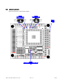
1
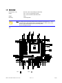
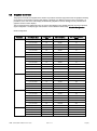
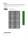
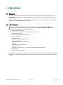
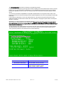
Cool SpaceRunner-LX800
PC/104-Plus CPU Board
Technical Manual
TME-104P-CSR-LX800-R1V11.doc
Revision 1.11 / April 11
©LiPPERT Embedded Computers GmbH
Hans-Thoma-Str. 11
D-68163 Mannheim
http://www.lippertembedded.com/
Technical Manual Cool SpaceRunner-LX800
LiPPERT Document: TME-104P-CSR-LX800-R1V11 Revision 1.11
Copyright ©2011 LiPPERT Embedded Computers GmbH, All rights reserved
Contents and specifications within this manual are subject of change without notice.
Trademarks
MS-DOS, Windows, Windows 95, Windows 98, Windows NT and Windows XP are trademarks of Microsoft
Corporation. PS/2 is a trademark of International Business Machines, Inc. Intel and Solid State Drive are
trademarks of Intel Corporation. Geode is a trademark of Advanced Micro Devices. PC/104 is a registered
trademark of PC/104 Consortium. All other trademarks appearing in this document are the property of their
respective owners.
Disclaimer
Contents and specifications within this technical manual are subject of change without notice.
LiPPERT Embedded Computers GmbH provides no warranty with regard to this technical manual or any other
information contained herein and hereby expressly disclaims any implied warranties of merchantability or fitness
for any particular purpose with regard to any of the foregoing. LiPPERT Embedded Computers GmbH assumes no
liability for any damages incurred directly or indirectly from any technical or typographical errors or omissions
contained herein or for discrepancies between the product and the technical manual. In no event shall LiPPERT
Embedded Computers GmbH be liable for any incidental, consequential, special, or exemplary damages, whether
based on tort, contract or otherwise, arising out of or in connection with this user’s guide or any other information
contained herein or the use thereof.
Table of Contents
1
1.1
1
Overview
Introduction ............................................................................................... 1
Features .................................................................................................... 1
Block Diagram ............................................................................................. 2
1.2
Ordering Information .................................................................................... 3
Cool SpaceRunner-LX800 Models ..................................................................... 3
Cable Sets and Accessories ............................................................................ 3
1.3
Specifications............................................................................................. 4
Electrical Specifications ................................................................................. 4
Environmental Specifications ........................................................................... 4
Mean Time Between Failures ........................................................................... 4
1.4
2
2.1
Mechanical ................................................................................................ 5
6
Getting Started
Connector Locations .................................................................................... 6
Top .......................................................................................................... 6
Bottom ...................................................................................................... 7
2.2
Jumper Locations ........................................................................................ 8
2.3
LED indicators ............................................................................................ 9
2.4
Hardware Setup ........................................................................................ 10
3
11
Module Description
3.1
Processor ............................................................................................... 11
3.2
Companion .............................................................................................. 12
3.3
Graphics-Controller.................................................................................... 13
VGA Connector ........................................................................................... 14
LVDS Configuration...................................................................................... 15
LVDS Connector ......................................................................................... 15
LVDS Color Mapping .................................................................................... 16
Backlight Connector ..................................................................................... 16
Display Voltage Jumpers ............................................................................... 17
3.4
EIDE Solid State Drive ................................................................................ 17
TME-104P-CSR-LX800-R1V11.doc
Rev 1.11
i
3.5
Ethernet Controller ..................................................................................... 18
Ethernet Interface ........................................................................................ 18
3.6
On Board Power Supply .............................................................................. 19
Power Connector ........................................................................................ 19
3.7
EIDE Port ................................................................................................ 20
EIDE Connector .......................................................................................... 20
3.8
PS/2 Interface .......................................................................................... 21
Keyboard and Mouse Connector ..................................................................... 21
3.9
USB 2.0 Ports .......................................................................................... 21
USB 2.0 Connector 0.................................................................................... 22
USB 2.0 Connector 1/2/3 ............................................................................... 22
3.10
Serial Ports .............................................................................................. 23
COM1/2 Connector ...................................................................................... 23
RS485-Termination Jumpers .......................................................................... 24
3.11
Parallel Port LPT ....................................................................................... 24
LPT Connector ........................................................................................... 25
3.12
Speaker .................................................................................................. 26
3.13
External Power-Button ................................................................................ 26
3.14
Reset-In Signal ......................................................................................... 27
3.15
Internal Battery ......................................................................................... 27
3.16
External Battery ........................................................................................ 27
3.17
PC/104-Plus Bus Interface ........................................................................... 28
PC/104 Plus Bus Connector ........................................................................... 29
3.18
PC/104 Bus Interface ................................................................................. 30
PC/104 Bus Connector ................................................................................. 30
3.19
4
BIOS Recovery ......................................................................................... 31
32
Using the Module
4.1
Watchdog ............................................................................................... 32
4.2
LEMT functions ......................................................................................... 32
4.3
BIOS...................................................................................................... 33
Battery Jumper ........................................................................................... 33
Configuring the XpressROM BIOS .................................................................... 33
TME-104P-CSR-LX800-R1V11.doc
Rev 1.11
ii
Trouble Shooting BIOS Settings ...................................................................... 41
4.4
Drivers ................................................................................................... 42
4.5
Programming Examples .............................................................................. 43
LIVE-LED .................................................................................................. 43
Watchdog ................................................................................................. 44
Reading Temperatures .................................................................................. 45
Reading Voltages ........................................................................................ 46
5
47
Address Maps
5.1
Memory Address Map ................................................................................ 47
5.2
I/O Address Map ....................................................................................... 48
5.3
Interrupts ................................................................................................ 49
5.4
DMA Channels.......................................................................................... 49
5.5
PC/104 Bus Address Space ......................................................................... 50
Appendix A, Contact Information
A
Appendix B, Additional Information
B
Appendix C, Getting Help
C
Appendix D, Revision History
D
TME-104P-CSR-LX800-R1V11.doc
Rev 1.11
iii
Acronyms
ACPI
AES
APM
ATA
BIOS
BPP
CD
COM
CPU
CRT
CSR
DAC
DDR
DMA
DOT
EIDE
EMC
ETH
FIFO
FPU
FWH
GPIO
HDD
I²C
IP
ISA
LCD
LEMT
LED
LPC
LVDS
MAC
MMU
PCI
PHY
PLL
PS/2
PWR
SMB
SMC
SPI
SSD
SVGA
TCP
TLB
UART
USB
UDMA
UDP
VGA
WDOG
Advanced Configuration and Power Management Interface
Advanced Encryption Standard
Advanced Power Management
Advanced Technology Attachment
Basic Input Output System
Bits Per Pixel
Compact Disc
Communication Equipment
Central Processing Unit
Cathode Ray Tube
Cool SpaceRunner
Digital-to-Analog-Converter
Double Date Rate
Direct Memory Access
Dynamic Overclocking Technology
Enhanced Integrated Device Electronics
Electromagnetic Compatibility
Ethernet
First In First Out
Floating Point Unit
Firmware Hub
General Purpose Input Output
Hard Disk Drive
Inter-Integrated Circuit
Internet Protocol
Industry Standard Architecture
Liquid Crystal Display
LiPPERT Enhanced Management Technology
Light Emitting Diode
Low Pin Count
Low Voltage Differential Signaling
Media Access Control
Memory Management Unit
Peripheral Component Interconnect
Physical Interface
Phase-Locked Loop
Personal System/2
Power
System Management Bus
System Management Controller
Serial Peripheral Interface
Solid State Drive
Super Video Graphics Array
Transmission Control Protocol
Translation Look-aside Buffer
Universal Asynchronous Receiver Transmitter
Universal Serial Bus
Ultra-Direct Memory Access
User Datagram Protocol
Video Graphics Array
Watchdog
TME-104P-CSR-LX800-R1V11.doc
Rev 1.11
iv
1 Overview
1.1
Introduction
The Cool SpaceRunner-LX800 is a CPU-board for especially designed with rugged appliances in mind. It allows
the design of devices without moving parts. Additional resilience comes from the used through-hole connectors.
The PC/104-Plus board with AMD’s Geode™ LX processor has a very good performance to power ratio. The
board comprises all peripherals needed for an embedded PC on a small 3.775" by 4.050" printed circuit board. It
is fully plug-in compatible with the Cool SpaceRunner 2, except that the Flat Panel connector is replaced with
three USB 2.0 ports.
The Cool SpaceRunner-LX800 integrates a powerful yet efficient AMD Geode™ LX800 processor together with a
CS5536 I/O companion and a Super I/O chip to form a complete PC, with all the standard peripherals already
onboard. There is a graphics controller with VGA and LVDS adapters to connect different sorts of display
terminals. Backlighting is provided for LCD modules too.
A fast 100/10BaseT Ethernet port, two RS232/RS422/RS485 serial ports, and four USB 2.0 host ports handle the
communication with external devices. There are PS/2 connectors for keyboard and mouse as well as a parallel
printer port available. An IDE ATA100 adapter allows connection of hard disk or CD drives. Applications that
require non-moving storage can use the integrated Solid State Drive.
There is Solid State Drive (SSD) integrated, which is connected to the ATA-controller.
System expansion can easily be realized over PC/104, PC/104-Plus and I²C bus connectors.
The Cool SpaceRunner-LX800 is powered by a 5V-only supply and supports ACPI, advanced power management
and PCI power management. Security critical applications take advantage of the Geode LX800 processor, too. It
has an on-chip AES 128-bit crypto acceleration block capable of 44 Mbps throughput on either encryption or
decryption. The AES block runs asynchronously to the processor core and is DMA based.
The Cool SpaceRunner-LX800 runs DOS, Windows, Linux and VxWorks operating systems.
Features
CPU
Main Memory
·
·
·
·
·
·
· soldered 256 MB DDR SDRAM 400 MHz
AMD Geode™ LX 800@0,9W (500MHz)
Cache Memory with:
64 KB/64 KB level 1 I/D caches
TLB (Translation Look-aside Buffer):
128 KB level 2 cache
Efficient Prefetch
Chipset
Extension slots
· AMD CS5536 companion device
· 1 x 32-bit PC/104-Plus
· 1 x 16-bit PC/104 with full DMA capability
Interfaces
·
·
·
·
·
·
Ethernet 10/100BaseT
ATA-6 EIDE (Ultra DMA-100)
PS/2 Keyboard/Mouse
4 x USB 2.0 ports
2 x RS232/RS485/RS422, software selectable
1 x parallel port
· SVGA monitor
· 18/24 Bit LVDS for displays
· MISC signals: external power button, I²C bus,
speaker, external reset button, external battery
connector
· Power supply
· Solid Sate Drive on EIDE
Other configurations are possible at high volumes.
TME-104P-CSR-LX800-R1V11.doc
Rev 1.11
1 (50)
Block Diagram
COM1
RS232/485
IDC 10
2.54 mm
LPT/ Parallel
IDC 26
2.54 mm
Line Driver
LTC1334
Super I/O
ITE8712
COM2
RS232/485
IDC 10
2.54 mm
Line Driver
LTC1334
PS/2-MS/KB
MISC
IDC 10
2.54 mm
PS/2
SMC
UPD78F0511GA
LPC
FWH
DF13 10 pin
1.25 mm
SST FWH
SST25LF080A
SPI
SMB
EIDE
IDC 44
2.00 mm
EIDE
SSD
2GB
USB1/2/3
IDC12
2.54 mm
I/O Companion
CS5536
USB0
Ethernet1
IDC 10
2.54 mm
ETH
Intel 82551IT
PCI
PCI -> ISA
ITE8888
VGA
IDC 10
2.54 mm
ISA
PCI
PC/104 Plus
Backlight
DF13 8 pin
1.25 mm
AMD Geode LX800
LVDS DF14
2 x 10 pin
1.25 mm
Transmitter
DS90C383B
PC/104
Memory
256 MB
CSR-LX800 PC/104- Diagram
rev1v2 10072008CS
TME-104P-CSR-LX800-R1V11.doc
Rev 1.11
2 (50)
1.2
Ordering Information
Cool SpaceRunner-LX800 Models
Order number
Description
903-0019-10
Cool SpaceRunner-LX800 with LCD+VGA-CRT, AMD GEODE [email protected] (500 MHz), low
power consumption, 256MB DDR SDRAM, 4x USB2.0, IrDA, RTC, Battery, EIDE, 3x COM,
LPT (EPP/EPC), PS/2 Keyboard, PS/2 Mouse, WDOG, LEMT, PC/104 bus, PC/104+ bus,
VGA controller and LVDS Interface, Fast Ethernet 100/10BaseT, EIDE 2 GB SSD
Operating temperature range: -40°C…+85°C
Cable Sets and Accessories
There are some options offered for the Cool SpaceRunner-LX800.
Order number
Description
863-0014-10
Adapter Cable Set
Power, PS/2 keyboard and mouse, Ethernet and USB, VGA-CRT, 3x USB, COM1, COM2,
LPT, IDE (44 pin, 2mm), cable adapter 2.5" > 3.5", adapter 3.5" > 2.5"
TME-104P-CSR-LX800-R1V11.doc
Rev 1.11
3 (50)
1.3
Specifications
Electrical Specifications
Supply voltage
+5 V DC
Rise time
< 10 ms
Supply voltage tolerance
± 5%
Inrush current
6.5 A, 25µs
Supply current
maximal 0.95 A (Memtest86 v1.70)
typical 0.6 A (Windows XP idle mode)
typical 0.2 A (suspend to ram mode)
1
2
Environmental Specifications
Operating:
Temperature range
-20 … 60 °C (standard version)
-40 … 85 °C (extended version)
Temperature change
max. 10K / 30 minutes
Humidity (relative)
10 … 90 % (non-condensing)
Pressure
450 … 1100 hPa
Non-Operating/Storage/Transport:
Temperature range
-40 … 85 °C
Temperature change
max. 10K / 30 minutes
Humidity (relative)
5 … 95 % (non-condensing)
Pressure
450 … 1100 hPa
Mean Time Between Failures
MTBF at 25°C
1
294 173 hours
With that tolerance is not mentioned that all plugged devices are running with.
2
That rate of current is possible when only monitor, mouse and keyboard are plugged.
If there are connected additional peripheral devises the current rises up.
TME-104P-CSR-LX800-R1V11.doc
Rev 1.11
4 (50)
1.4
Mechanical
Dimensions (L x W)
95.9 mm x 90.2 mm (including I/O extension)
Height
max. 14 mm on top side above PCB
max. 12 mm on bottom side above PCB
Weight
100 g
Mounting
4 mounting holes
Note: It is strongly recommend using plastic spacers instead of metal spacers to mount
the board. With metal spacers, there is a possible danger to create a short circuit
with the components located around the mounting holes.
This can damage the board!
TOP
Pin1
TME-104P-CSR-LX800-R1V11.doc
Pin2
Rev 1.11
5 (50)
2 Getting Started
2.1
Connector Locations
Top
(Click on the blue font to reach the right chapter.)
LPT
X15
COM1
X11
COM2
X12
PC/104
Plus
X17
PC/104
X18
PWR
X19
LVDS
X7
Backlight
X6
ETH/USB0
X9
USB1/2/3
X8
VGA
X3
EIDE
X10
PS/2
X16
The connectors' pin 1 is marked RED
TME-104P-CSR-LX800-R1V11.doc
Rev 1.11
6 (50)
Bottom
PC/104
Plus
X17
PC/104
X18
The connectors' pin 1 is marked RED
TME-104P-CSR-LX800-R1V11.doc
Rev 1.11
7 (50)
2.2
Jumper Locations
(Click on the blue font to reach the right chapter.)
Jumper
COM1 termination
X13
Pin 1
Pin 3
Pin 2
Pin 4
Jumper
COM2 termination
X14
Pin 1
Pin 3
Pin 2
Pin 4
Jumper
Battery
X30
Jumper
LVDS and Backlight Power Supply
X5
TME-104P-CSR-LX800-R1V11.doc
Rev 1.11
8 (50)
2.3
LED indicators
The onboard LED indicators provide a very comfortable way to check the board’s status. The boot success,
power status, IDE accesses, Watchdog and Ethernet accesses are all visible.
The LED indicators are located on top of the board, near the PC/104 connector.
LINK
Green LED shows the Ethernet Link status.
ACT
Red LED flashes at Ethernet activity.
Speed
Yellow LED lights up if 100Mbit connection is established.
MAIN
Green LED lights up when Main Power is supplied.
PM
Power Mode
Green LED is constantly lit if the boot process is complete and the
board is running normally.
LED flashes when board goes in suspend to ram mode.
SBY
Green LED lights up when Standby Power is supplied.
LIVE
Red LED is on at startup while the board executes the BIOS power
on self test (POST). After that it is freely usable by application
programs. Chapter "LIVE-LED" shows a small sample program how
to control it.
IDE
Yellow LED flashes when IDE activity is recognized.
WD
Red LED lights up when Watchdog was triggered. Can only be reset by a power off sequence.
TME-104P-CSR-LX800-R1V11.doc
Rev 1.11
9 (50)
2.4
Hardware Setup
Caution
Be sure to observe the EMC security measures. Make sure you are always at the
same potential as the module.
Caution
Never connect or disconnect peripherals like HDD's, PCI, and ISA boards while
the board's power supply is connected and switched on!
Use the cable set provided by LiPPERT to connect the Cool SpaceRunner-LX800 to a VGA monitor. Connect
either PS/2 or USB keyboard or mouse, respectively. Use the 44-wire cable to connect the hard disk. Make sure
that the pins match their counterparts correctly and are not twisted! If you plan to use additional other peripherals,
now is the time to connect them, too.
Set the “Jumper Battery” that it has contact with both pins. The location can be found on chapter 2.2.
Connect a 5 volt power supply to the power connector and switch the power on.
Note
In continuous mode there only about 1 amp necessary,
but at power on there are more than 6,5 A inrush current required.
The display shows the BIOS messages. If you want to change the standard BIOS settings, press the <F1> key to
enter the BIOS menu. See chapter 4.3 for setup details.
If you need to load the BIOS default values, they can be automatically loaded at boot time. See chapter "Trouble
Shooting BIOS Settings", about how to do it.
The Cool SpaceRunner-LX800 boots from CD drives, USB floppy, USB stick, or hard disk. Provided that any of
these is connected and contains a valid operating system image, the display then shows the boot screen of your
operating system.
The Cool SpaceRunner-LX800 does not need any cooling measures, neither at standard environment
temperatures from –20 °C … +60 °C nor in the extended range of -40 °C ... +85 °C.
TME-104P-CSR-LX800-R1V11.doc
Rev 1.11
10 (50)
3 Module Description
3.1
Processor
The AMD Geode LX [email protected] processor delivers one of the best performance-per-watt figures in the industry,
providing x86 power and versatility to embedded products. Its architecture and high level of integration
guarantees longer battery life and allows very small designs, while delivering full x86 functionality.
The AMD Geode LX 800 processor consumes a maximum power of 3.9W and 1.8W typical at 500 MHz, enabling
systems that only need to be passively cooled.
The x86 compatibility allow designers to focus on developing end products that efficiently meet consumer needs
without being concerned with software porting or compatibility issues.
Coupled with the AMD Geode™ CS5536 companion device, the combined chipset, which operates at 1.9W
typical at 433MHz and at 2.4W typical at 500MHz, offers a complete set of features that deliver full desktop
functionality to embedded and portable devices.
Internal block diagram of the LX 800 processor
TME-104P-CSR-LX800-R1V11.doc
Rev 1.11
11 (50)
Processor functional blocks are
·
CPU Core
·
GeodeLink™ Control Processor
·
GeodeLink Interface Units
·
GeodeLink Memory Controller
·
Graphics Processor
·
Display Controller
·
Video Processor
·
Video Input Port
·
GeodeLink PCI Bridge
·
Security Block
For further information please refer to the data book of the AMD Geode LX 800
TM
P
3.2
P
P
Companion
AMD Geode™ CS5536 companion device
The AMD Geode™ CS5536 companion device is designed to work with an integrated processor North Bridge
component such as the AMD Geode™ GX/LX processor. Together, the Geode GX/LX processor and Geode
CS5536 companion device provide a system-level solution well suited for the high-performance and low-power
needs of a host of embedded devices including digital set-top boxes, mobile computing devices, thin client
applications, and single board computers.
The internal architecture uses a single, high-performance modular structure based on GeodeLink™ architecture.
This architecture yields high internal speed (over 4 GB/s) data movement and extremely versatile internal power
management. The GeodeLink™ architecture is transparent to application software. Communication with the
Geode GX/LX processor is over a 33/66 MHz PCI bus.
The Geode CS5536 companion device incorporates many I/O functions, including some found in typical Super-I/O
chips, simplifying many system designs. Since the graphics subsystem is entirely contained in the Geode GX/LX
processor, system interconnect is simplified. The device contains state-of-the-art power management that
enables systems, especially battery powered systems, to significantly reduce power consumption.
Audio is supported by an internal controller, designed to connect to multiple AC97 compatible codecs. An IR
(infrared) port supports all popular IR communication protocols. The IR port is shared with one of two industrystandard serial ports that can reach speeds of 115.2 kbps. An LPC (low pin count) port is provided to facilitate
connections to a Super-I/O should additional expansion, such as a floppy drive, be necessary, and/or to an LPC
ROM for the system BIOS
The hard disk controller is compatible to the ATA-5 specification. The bus mastering IDE controller includes
support for two ATA-compliant devices on one channel. The CS5536 companion device provides four Universal
Serial Bus (USB) 2.0 compliant ports, supporting low speed, full speed, and high speed connections. All four ports
are individually automatically associated with either the Open Host Controller Interface (OHCI) or the Enhanced
Host Controller Interface (EHCI) depending on the attached device type. A real-time clock (RTC) keeps track of
time and provides calendar functions.
A suite of 82xx devices provides the legacy PC functionality required by most designs, including two PIC's
(programmable interrupt controllers), one PIT (programmable interval timer) with three channels, and DMA (direct
memory access) functions. The CS5536 companion device contains eight MFGPT's (multi-function general
purpose timers) that can be used for a variety of functions. A number of GPIO's (general purpose input/outputs)
are provided, and are assigned to system functions on power-up.
State-of-the-art power management features are attained with the division of the device into two internal power
domains. The GPIO's and multi-function timers are distributed into each domain allowing them to act as wakeup
sources for the device. The device provides full ACPI (Advanced Configuration Power Interface) compliance and
supports industry-standard Wakeup and Sleep modes.
TME-104P-CSR-LX800-R1V11.doc
Rev 1.11
12 (50)
3.3
Graphics-Controller
The graphics controller is integrated in the Geode LX processor and does high performance 2D-graphics handling.
CRT monitors can be used as well as LVDS displays. Therefore, two different connectors are on the board. It is
possible to use a CRT and a LVDS display simultaneously (depends on drivers setting), but only with the same
graphics content on both displays.
The Cool SpaceRunner-LX800 supports 3,3V and 5V LVDS displays with 18/24bit interfaces and unconventional
signal configuration. The display type and resolution can be selected in BIOS setup: Graphics Configuration
SVGA Configuration
Resolution
Color Depth (bpp)
Refresh Rate
(Hz)
Dot Clock (MHz)
Min. GLIU Frequency
(MHz)
640 x 480
8, 16, or 24/32
60
25.175
75
8, 16, or 24/32
70
28.560
75
8, 16, or 24/32
72
31.500
75
8, 16, or 24/32
75
31.500
75
8, 16, or 24/32
85
36.000
75
8, 16, or 24/32
90
37.889
400
8, 16, or 24/32
100
43.163
400
8, 16, or 24/32
60
40.000
75
8, 16, or 24/32
70
45.720
75
8, 16, or 24/32
72
49.500
75
8, 16, or 24/32
75
49.500
75
8, 16, or 24/32
85
56.250
75
800 x 600
1024 x 768
1152x864
1280 x 1024
8, 16, or 24/32
90
60.065
400
8, 16, or 24/32
100
68.179
400
8, 16 or 24/32
60
65.000
75
8, 16, or 24/32
70
75.000
100
8, 16, or 24/32
72
78.750
100
8, 16, or 24/32
75
78.750
100
8, 16, or 24/32
85
94.500
100
8, 16, or 24/32
90
100.187
400
8, 16, or 24/32
100
113.310
400
8, 16, or 24/32
60
81.600
100
8, 16, or 24/32
70
97.520
100
8, 16, or 24/32
72
101.420
200
8, 16, or 24/32
75
108.000
200
8, 16, or 24/32
85
119.650
200
8, 16, or 24/32
90
129.600
400
8, 16, or 24/32
100
144.000
400
8, 16, or 24/32
60
108.000
200
8, 16, or 24/32
70
129.600
200
8, 16, or 24/32
72
133.500
200
8, 16, or 24/32
75
135.000
200
TME-104P-CSR-LX800-R1V11.doc
Rev 1.11
13 (50)
Resolution
Color Depth (bpp)
Refresh Rate
(Hz)
Dot Clock (MHz)
Min. GLIU Frequency
(MHz)
8, 16, or 24/32
85
157.500
200
1600 x 1200
1920x1440
8, 16, or 24/32
90
172.800
400
8, 16, or 24/32
100
192.000
400
8, 16, or 24/32
60
162.000
200
8, 16, or 24/32
70
189.000
200
8, 16, or 24/32
72
198.000
233
8, 16, or 24/32
75
202.500
233
8, 16, or 24/32
85
229.500
266
8, 16, or 24/32
90
251.182
400
8, 16, or 24/32
100
280.640
400
8, 16, or 24/32
60
234.000
266
8, 16, or 24/32
70
278.400
400
8, 16, or 24/32
72
288.000
400
8, 16, or 24/32
75
297.000
400
8, 16, or 24/32
85
341.349
400
VGA Connector
Connector type:
Matching connector:
IDC10 pin header 2.54 mm
IDC10 pin female connector 2.54 mm
Pin
Signal
Pin
Signal
1
Red
2
GND
3
Green
4
GND
5
Blue
6
GND
7
HSYNC
8
GND
VSYNC
10
GND
9
X3
TME-104P-CSR-LX800-R1V11.doc
Rev 1.11
14 (50)
LVDS Configuration
The display options of LVDS are shown in the table:
Setting
Possible Values
Flat Panel Type
Resolution
LVDS
320x240, 640x480, 800x600, 1024x768,
1152x864, 1280x1024, 1600x1200
Data Bus Type
18/24 Bits, 2ppc
Refresh Rate
60 70, 72, 75, 85, 90, 100 Hz
HSYNC Polarity
High, Low
VSYNC Polarity
High, Low
LP Active Period
Active Only
Free Running
à only active during SYNC
à always active
SHFCLK Active Period
Active Only
Free Running
à only active during SYNC
à always active
To ease usage of these displays it’s possible to select the display and backlight supply voltages with the onboard
voltage selector jumpers. (Jumper LVDS and Backlight, see below)
LVDS Connector
Connector type:
Matching connector:
Pin
Signal
2
SW-VDD
4
6
8
3
Hirose DF13 2x 10-pin header
Hirose DF13-20DS-1.25C, part number 536-0555-6 00
Pin
Signal
1
SW-VDD
GND
3
GND
TX3+
5
TX3GND
3
3
TXCLK-
7
10
GND
9
TXCLK+
12
TX2+
11
TX2-
14
TX1-
13
GND
16
GND
15
TX1+
18
TX0+
17
TX0-
20
DDC DATA
19
DDC CLK
X7
1.0 A is the maximum current for each pin
TME-104P-CSR-LX800-R1V11.doc
Rev 1.11
15 (50)
LVDS Color Mapping
Backlight Connector
Connector type:
Matching connector:
Hirose DF13 8 pin
Hirose DF13-8S-1.25C, part number 536-0007-0 00
Pin
Signal
1
+12 Volt
4
2
+12 Volt
4
3
+5 Volt
4
4
+5 Volt
4
5
EN
6
VCC
7
GND
8
GND
5
4
0.5 A is the maximum current for each pin
5
That voltage can be selected using the jumper "Backlight", shown on next page.
TME-104P-CSR-LX800-R1V11.doc
Rev 1.11
X6
16 (50)
Display Voltage Jumpers
Jumper LVDS and Backlight
Connector type:
Matching part:
IDC6 pin header 2.0 mm
2.0 mm jumper
Use a 2 mm jumper between 1-3 or 3-5 to select the backlight voltage.
Use a 2 mm jumper between 2-4 or 4-6 to select the display voltage.
Pin
Signal
Pin
Signal
1
+12 Volt
2
+5 Volt
3
Backlight voltage
4
Display voltage
5
+ 5 Volt
6
+3.3 Volt
X5
default jumper setting
Backlight
Jumper
1-3
3-5
+12V
+5V
Jumper
2-4
4-6
Power supply
+5V
+3.3V
Power supply
LVDS
Note:
3.4
An arrow on the PCB marks Pin 1
EIDE Solid State Drive
On the top side of the board, the SSD is mounted. It can be used instead of a hard disk. Per default, it is defined
as master but that can be changed in BIOS.
The SSD, manufactured by SST, is built as a flash storage organized of Single Level Cells (SLC). It can be erased
over 100M times without losing capacity. The wear-leveling feature can increase that number, depending on the
allocation of the disk space.
Product features:
Read Bandwidth
30 Mbytes/s
Write Bandwidth
20 Mbytes/s
Access time
0.2 ms
PATA Compatibility
ATA-5; PIO 0-4; DMA 0-2; UDMA 0-4
Power Control
Automatic power down during wait periods
Automatic sleep mode during host inactivity
NAND Management
TME-104P-CSR-LX800-R1V11.doc
Active wear-leveling algorithm
Rev 1.11
17 (50)
3.5
Ethernet Controller
Intel 82551IT Fast Ethernet Controller
The 82551IT is an evolutionary addition to Intel’s family of 8255x controllers. It provides excellent performance by
offloading TCP, UDP and IP checksums and supports TCP segmentation off-load for operations such as Large
Send. The 82551IT provides an extended operating temperature in addition to all of the same capabilities and
features as the 82551ER to address applications requiring a wider operating temperature range.
Its optimized 32-bit interface and efficient scatter-gather bus mastering capabilities enable the 82551IT to perform
high speed data transfers over the PCI bus. This capability accelerates the processing of high level commands
and operations, which lowers CPU utilization. Its architecture enables data to flow efficiently from the bus interface
unit to the 3 KB Transmit and Receive FIFO's, providing the perfect balance between the wire and system bus. In
addition, multiple priority queues are provided to prevent data underruns and overruns.
The 82551IT includes both a MAC and PHY. In also has a simple interface to the analog front end, which allows
cost effective designs requiring minimal board real estate. The 82551IT is pin compatible with the 82559 family of
controllers and is offered with software that provides backwards compatibility with previous 8255xER controllers.
Ethernet Interface
The Ethernet connector is shared with USB 0 and I²C bus.
Connector type:
Matching connector:
IDC10 pin header 2.54 mm
IDC10 pin female connector 2.54 mm
Pin
Signal
Pin
Signal
1
ETH1-TX+
2
ETH1-TX-
3
ETH1-RX+
4
SMB_DATA
5
SMB_CLK
6
ETH1-RX-
7
USB0+
8
USB0-
9
VCC_USB0
10
USB-GND
X9
TME-104P-CSR-LX800-R1V11.doc
Rev 1.11
18 (50)
3.6
On Board Power Supply
The on board power controllers generate all necessary voltages from the single supply voltage
of 5 Volt. The generated 3.3 Volt is available at Backlight- and LVDS- connector.
Note
This 3.3 V cannot be used to supply external electronic devices with high power
consumption like other PC/104 boards or displays.
Power Connector
Connector type:
Matching connector:
Note
JST B15B-EH-A 15 pin
JST EHR-15 15 pin female connector
Pin
Signal (standard)
Signal (5V only)
1
+5 V
+5V
2
GND
GND
3
+5V
+5V
4
GND
GND
5
+5V
+5V
6
n.c.
n.c.
7
GND
GND
8
GND
GND
9
n.c.
n.c
10
n.c.
n.c
11
GND
GND
12
+12V
n.c
13
+12V
n.c
14
GND
GND
15
-12V
n.c
X19
The default cable adapter supports the connection of ±12V power supply.
That pins are routed to the PC/104- , PC/104-plus bus as well as the backlight port.
If the 5 V only power supply is required leave these pins open.
The board can be supplied over the 5 V pins of the PC/104- or PC/104 plus bus too.
TME-104P-CSR-LX800-R1V11.doc
Rev 1.11
19 (50)
3.7
EIDE Port
An EIDE port is provided by the chipset to connect one drive. The connected device can be set as master and
slave, depending on the SSD mode.. To enhance the performance, this port has a 100 MB/s IDE controller in
UDMA mode per the ATA-5 specification The EIDE port is available on a standard 44-pin header (2 mm) for 2.5"
hard disks.
Only one more EIDE device can be connected, one slot is reserved for the SSD.
EIDE Connector
Connector type
Matching connector:
IDC44 pin header 2.00 mm
IDC44 pin female connector 2.00 mm
Pin
Signal
Pin
Signal
1
Reset#
2
GND
3
Data7
4
Data8
5
Data6
6
Data9
7
Data5
8
Data10
9
Data4
10
Data11
11
Data3
12
Data12
Data13
13
Data2
14
15
Data1
16
Data14
17
Data0
18
Data15
19
GND
20
NC
GND
21
DRQ0
22
23
Write
24
GND
25
Read
26
GND
27
Ready
28
CSEL
GND
29
DACK0
30
31
IRQ
32
IOCS16-
33
Address1
34
PD66
35
Address0
36
Address2
CS3
37
6
CS1
38
39
NC
40
GND
41
+5 Volt
42
+5 Volt
43
GND
44
GND
6
X10
6
0,8 A is the maximum current for each pin
TME-104P-CSR-LX800-R1V11.doc
Rev 1.11
20 (50)
3.8
PS/2 Interface
PS/2-connectors for mouse and keyboard are shared with several system signals.
An adapter cable for the PS/2 devices is available.
Keyboard and Mouse Connector
Connector type:
Matching connector:
3.9
IDC10 pin header 2.54 mm
IDC10 pin female connector 2.54 mm
Pin
Signal
Pin
Signal
1
Speaker
2
Mouse Clock
3
Reset-In
4
Mouse Data
5
KB Data
6
KB Clock
7
GND
8
+5 Volt Switched
9
Ext. Battery
10
Power Button
7
X16
USB 2.0 Ports
Four standard USB 2.0 host ports are provided with the Cool SpaceRunner-LX800. Three are located on the
IDC12 header "USB". An adapter cable is available to use standard USB devices with this connector.
The other one is located on the IDC10 header "Ethernet". A standard adapter cable is available, too.
It is possible to use an USB keyboard under MSDOS without special driver software.
Note:
7
Not all USB keyboard models are supported.
0.5 A is the maximum current for each pin; power supply will be switched off in standby mode
TME-104P-CSR-LX800-R1V11.doc
Rev 1.11
21 (50)
USB 2.0 Connector 0
Connector type:
Matching connector:
IDC10 pin header 2.54 mm
IDC10 pin female connector 2.54 mm
Pin
Signal
Pin
1
ETH1-TX+
2
ETH1-TX-
3
ETH1-RX+
4
SMB_DATA
5
SMB_CLK
6
ETH1-RX-
7
USB0+
8
USB0-
9
VCC_USB0
10
USB-GND
8
Signal
X9
USB 2.0 Connector 1/2/3
Connector type:
Matching connector:
IDC12 pin header 2.54 mm
IDC12 pin female connector 2.54 mm
Pin
8
Signal
1
VCC_USB1
3
USB1+
5
VCC_USB2
7
USB2+
9
VCC_USB3
11
USB3+
8
8
8
Pin
Signal
2
USB-GND
4
USB1-
6
USB-GND
8
USB2-
10
USB-GND
12
USB3-
X8
0.5 A is the maximum current for that pin; power supply will be switched off in standby mode
TME-104P-CSR-LX800-R1V11.doc
Rev 1.11
22 (50)
3.10 Serial Ports
The maximum supported baud rates:
RS485 mode
RS232 mode
1,5 Mbit/s
115 kbit/s
9
The serial ports are located on two IDC headers "COM1" and "COM2". Adapter cables with standard DSUB-9
male connectors are available. The ports either work in RS232 or RS485 mode, selectable in BIOS.
When entering Serial and Parallel Device Configurations, COM Port 1 Mode and COM Port 2 Mode can be
selected. Termination resistors for RS485 Mode can be set with Jumpers on pin headers as described in this
chapter.
To enable the transmitters of COM1 and COM2 in RS485 mode set the RTS# signal to ‘1’. Depending on your
operating system driver’s logic, this may mean setting a (non-inverted) RTS bit to ‘0’ in your application software.
The serial ports are programmable in BIOS setup. When entering Serial and Parallel Device Configurations,
configuration of the serial ports is accessible.
The following settings are possible for COM1 and COM2:
·
Disabled
·
3F8 / IRQ4 (base address / interrupt channel)
·
2F8 / IRQ3 (base address / interrupt channel)
·
3E8 / IRQ4 (base address / interrupt channel)
·
2E8 / IRQ3 (base address / interrupt channel)
The modes can be switched between RS232 and RS485.
COM1/2 Connector
Connector type:
Matching connector:
IDC10 pin header 2.54 mm
IDC10 pin female connector 2.54 mm
Pin
RS232
RS485
Pin
RS232
RS485
1
DCD
Not
used
2
DSR
RXD+
3
RXD
RXD-
4
RTS
TXD+
5
TXD
TXD-
6
CTS
Not used
7
DTR
Not
used
8
Not used
Not used
9
GND
GND
10
+5 Volt
+5 Volt
10
10
X11, X12
9
10
That baud rate requires changing registers manually, it is not supported by the default driver
0.5 A is the maximum current for that pin
TME-104P-CSR-LX800-R1V11.doc
Rev 1.11
23 (50)
RS485-Termination Jumpers
Connector type:
Matching connector:
IDC4 pin header 2.0 mm
IDC4 pin female connector 2.0 mm
Use 2 mm jumpers to terminate lines correctly.
There are two jumpers COM1 and COM2, respectively.
The RS485 termination jumpers are located at the top of the printed circuit board, see chapter 2.2
Pin
Signal
Pin
Signal
1
TX+
2
TX-
3
RX+
4
RX-
X13, X14
When the jumper is set, the differential pairs
are terminated with 120W between them.
(e.g. RX+ and RX-)
Additionally, positive/negative receive lines are pulled up/down with 1kW to
5V/GND in order to protect the transceivers of the Cool SpaceRunnerLX800 from over voltage.
It is recommended to protect the ports of the external device in the same
way!
Caution:
Termination Resistors should not be used in RS232 Mode!
Otherwise, the serial ports will not work.
3.11 Parallel Port LPT
The parallel port is located on an IDC26 header. An adapter cable with a standard DSUB-25 female connector is
available.
The parallel port is programmable in BIOS.
Entering Motherboard Device Configuration à Serial and Parallel Device Configurations, configuration of LPT is
accessible.
LPT Parameter
Base Address
Mode
Possible Settings
Disabled, 0x378
0x3BC and 0x278 are not recommended, because of a possible
conflict with the PCI to ISA Bridge
Compatible, PS/2 Bi-directional, EPP 1.7, EPP 1.9
IRQ
Disabled, IRQ 5, IRQ 7, IRQ 9, IRQ 10, IRQ 11
DMA
None, Channel 1, Channel 3
TME-104P-CSR-LX800-R1V11.doc
Rev 1.11
24 (50)
LPT Connector
Connector type:
Matching connector:
IDC26 pin header 2.54 mm
IDC26 pin female connector 2.54 mm
Pin
Signal
Pin
Signal
1
Strobe
2
Auto LF
3
Data0
4
Error
5
Data1
6
Init
7
Data2
8
Select In
9
Data3
10
GND
11
Data4
12
GND
13
Data5
14
GND
15
Data6
16
GND
17
Data7
18
GND
19
ACK
20
GND
21
Busy
22
GND
23
Paper End
24
GND
25
Select
26
+5Volt
11
X15
11
0.5 A is the maximum current for that pin
TME-104P-CSR-LX800-R1V11.doc
Rev 1.11
25 (50)
3.12 Speaker
The speaker signal is located on the IDC10 Header PS/2. A standard PC
Speaker can be connected between the signal SPEAKER and VCCKB.
Connector type:
Matching connector:
IDC10 pin header 2.54 mm
IDC10 pin female connector 2.54 mm
Pin
Signal
Pin
Signal
1
Speaker
2
Mouse Clock
3
Reset-In
4
Mouse Data
5
KB Data
6
KB Clock
7
GND
8
+5 Volt Switched
9
Ext. Battery
10
Power Button (default)/
Reset-In
12
X16
3.13 External Power-Button
The Power-Button signal is located on the IDC10 Header PS/2. To power up/down the board the signal PowerButton must be pulled to GND. It is not available in standard configuration.
Connector type:
Matching connector:
12
IDC10 pin header 2.54 mm
IDC10 pin female connector 2.54 mm
Pin
Signal
Pin
Signal
1
Speaker
2
Mouse Clock
3
Reset-In
4
Mouse Data
5
KB Data
6
KB Clock
7
GND
8
+5 Volt Switched
9
Ext. Battery
10
Power Button
X16
0.5 A is the maximum current for each pin; power supply will be switched off in standby mode
TME-104P-CSR-LX800-R1V11.doc
Rev 1.11
26 (50)
3.14 Reset-In Signal
The "Reset-In" signal is located on the IDC10 Header PS/2. To reset the board, the signal "Reset-In" must be
pulled to GND.
Connector type:
Matching connector:
IDC10 pin header 2.54 mm
IDC10 pin female connector 2.54 mm
Pin
Signal
Pin
Signal
1
Speaker
2
Mouse Clock
3
Reset-In
4
Mouse Data
5
KB Data
6
KB Clock
7
GND
8
+5 Volt Switched
9
Ext. Battery
10
Power Button
X16
3.15 Internal Battery
On the board a soldered battery type CR1225 is used to keep RTC time and date running if the board is not
powered. The battery can be connected or disconnected to the RTC with the battery jumper set to ON or OFF. As
default on delivery the jumper is set to OFF. It is recommended to set this jumper if the board is used in the
application and to remove the jumper if the board is stored for a longer period. This will prevent the battery from
discharge.
3.16 External Battery
A connected battery should replace or support the mounted one to keep date and time active during the board is
mechanical off.
It is recommended to use a model with 3 Volt, but it will also work with power suppliers up till 3,6 Volt.
The time and date will be lost if the power supplier falls down to 2,4 Volt.
For live time calculation there are 2 µA (25°C) needed when the board is not running.
That value can rise up with higher temperatures.
Connector type:
Matching connector:
IDC10 pin header 2.54 mm
IDC10 pin female connector 2.54 mm
Pin
Signal
Pin
Signal
1
Speaker
2
Mouse Clock
3
Reset-In
4
Mouse Data
5
KB Data
6
KB Clock
7
GND
8
+5 Volt Switched
9
Ext. Battery
10
Power Button
TME-104P-CSR-LX800-R1V11.doc
Rev 1.11
X16
27 (50)
3.17 PC/104-Plus Bus Interface
The PC/104-Plus bus is a modification of the standard PCI bus. It allows all of the PC/104 features to be used,
together with the high speed PCI bus.
The main features are:
·
PC/104-Plus Bus slot, fully compatible with PCI version 2.2 specifications.
·
Integrated PCI arbitration interface (32 bit wide, 3.3V).
·
Translation of PCI cycles to ISA bus.
·
Translation of ISA master initiated cycle to PCI.
·
Support for burst read/write from PCI master.
·
33 MHz PCI clock.
Note:
TME-104P-CSR-LX800-R1V11.doc
The 3.3 V pins on the PC/104 Plus bus connector are not supplied by the
onboard 3.3 V power supply. If a PC/104 Plus peripheral board is used that
needs 3.3V from the bus as power the customer must supply this voltage
by itself.
Rev 1.11
28 (50)
PC/104 Plus Bus Connector
Pin
A
B
C
D
1
GND
Reserved
+5 Volt
AD00
2
VI/O
AD02
AD01
+5 Volt
3
AD05
GND
AD04
AD03
4
C/BE0
AD07
GND
AD06
5
GND
AD09
AD08
GND
6
AD11
VI/O
AD10
M66EN
7
AD14
AD13
GND
AD12
8
n.c.
C/BE1
AD15
n.c.
9
SERR
GND
SB0
PAR
10
GND
PERR
n.c.
SDONE
11
STOP
n.c.
LOCK
GND
12
n.c.
TRDY
GND
DEVSEL
13
FRAME
GND
IRDY
n.c.
14
GND
AD16
n.c.
C/BE2
15
AD18
n.c.
AD17
GND
16
AD21
AD20
GND
AD19
17
n.c.
AD23
AD22
n.c.
18
IDSEL0
GND
IDSEL1
IDSEL2
19
AD24
C/BE3
VI/O
IDSEL3
20
GND
AD26
AD25
GND
21
AD29
+5 Volt
AD28
AD27
22
+5 Volt
AD30
GND
AD31
23
REQ0
GND
REQ1
VI/O
24
GND
REQ2
+5 Volt
GNT0
25
GNT1
VI/O
GNT2
GND
26
+5 Volt
CLK0
GND
CKL1
27
CLK2
+5 Volt
CLK3
GND
28
GND
INTD
+5 Volt
RST
29
+12 Volt
INTA
INTB
INTC
30
-12 Volt
REQ3
GNT3
GND
Note:
TME-104P-CSR-LX800-R1V11.doc
X17
All VI/O pins are connected to +3,3 V at default.
The voltages +5 V, +12 V and -12 V are not generated by the onboard
power-supply but they are routed from the Power Supply Connector.
The maximum current is limited depending on voltage:
+12 V < 1 A; -12 V < 0,3 A; +5 V < 8 A
One pin can be used for 1 A at maximum.
Rev 1.11
29 (50)
3.18 PC/104 Bus Interface
The PC/104 bus is a modification of the industry standard (ISA) PC bus specified in IEEE P996. The PC/104 bus
has different mechanics than P966 to allow the stacking of modules. The main features are:
·
Supports programmable extra wait state for ISA cycles
·
Supports I/O recovery time for back-to-back I/O cycles
The following table shows the pin assignment of the PC/104 connector.
PC/104 Bus Connector
Pin
0
1
2
3
4
5
6
7
8
9
10
11
12
13
14
15
16
17
18
19
D
GND
MEMCS16
IOCS16
IRQ10
IRQ11
IRQ12
IRQ15
IRQ14
DACK0
DRQ0
DACK5
DRQ5
DACK6
DRQ6
DACK7
DRQ7
+5 Volt
MASTER
GND
GND
Note:
TME-104P-CSR-LX800-R1V11.doc
C
GND
SBHE
LA23
LA22
LA21
LA20
LA19
LA18
LA17
MEMR
MEMW
SD8
SD9
SD10
SD11
SD12
SD13
SD14
SD15
KEY
Pin
1
2
3
4
5
6
7
8
9
10
11
12
13
14
15
16
17
18
19
20
21
22
23
24
25
26
27
28
29
30
31
32
A
IOCHCK
D7
D6
D5
D4
D3
D2
D1
D0
IOCHRDY
AEN
A19
A18
A17
A16
A15
A14
A13
A12
A11
A10
A9
A8
A7
A6
A5
A4
A3
A2
A1
A0
GND
B
GND
RSTDRV
+5 Volt
IRQ9
n.c.
DRQ2
-12 Volt
n.c.
+12 Volt
n.c.
SMEMW
SMEMR
IOW
IOR
DACK3
DRQ3
DACK1
DRQ1
REFRESH
SYSCLK
IRQ7
IRQ6
IRQ5
IRQ4
IRQ3
DACK2
TC
BALE
+5 Volt
OSC
GND
GND
X18
The voltages +5 V, +12 V and -12 V are not generated by the onboard
power-supply but they are routed from the Power Supply Connector.
The maximum current is limited depending on voltage:
+12 V < 1 A; -12 V < 0,3 A; +5 V < 3 A
One pin can be used for 1 A at maximum.
Rev 1.11
30 (50)
3.19 BIOS Recovery
Onboard there is a soldered SPI bios connected to an interface of the Super I/O IT8712.
Next to the PC104 header is a connector to plug in a recovery bios on the LPC bus.
If the system should boot from a connected FWH, the pin 6 "BIOS_DISABLE#" have to push to ground.
The mounted SPI BIOS will be disabled for booting activities and can be reprogrammed with a tool running in
DOS.
To program the SPI flash the FWH can be disconnected after the operation system is loaded successfully.
Connector type:
Matching connector:
13
Hirose DF13 10 pin header 1.25 mm
Hirose DF13-10S-1.25C, part number 536-0009-6 00
Pin
Signal
1
+3V3
2
LAD0
3
LAD1
4
LAD2
5
LAD4
6
BIOS_DISABLE#
7
LFRAME#
8
PCI_RST#
9
CLK_33_FWH_R
10
GND
13
0.3 A is the maximum current for that pin
TME-104P-CSR-LX800-R1V11.doc
Rev 1.11
31 (50)
4 Using the Module
4.1
Watchdog
A watchdog timer is integrated on-board and managed with the SMC LEMT functionality. There are different
possibilities for its activation. More details can be found in the next chapter where a detailed description of the
SMC can be found.
A watchdog event is triggered by internal circuit of the ITE8712 Super I/O. It is possible to program the trigger
duration, see chapter "Watchdog" for an example.
4.2
LEMT functions
The onboard Microcontroller implements power sequencing and LEMT (LiPPERT Enhanced Management
Technology) functionality. The microcontroller communicates via the System Management Bus with the
CPU/Chipset. The following functions are implemented:
·
Total operating hours counter
Counts the number of hours the module has been run in minutes.
·
On-time minutes counter
Counts the seconds since last system start.
·
Power cycles counter
·
Watchdog Timer
Set / Reset / Disable Watchdog Timer.
·
System Restart Cause
Power loss / Watchdog / External Reset.
·
Flash area
1kB Flash area for customer data
·
Protected Flash area
128 Bytes for Keys, ID's, etc. can stored in a write- and clear-protect able area.
·
Board Identify
Vendor / Board / Serial number
LEMT Tools are available for Windows and Linux, LEMT functionality can also be used in applications. Please ask
our support for the LEMT software manual and technical manual regarding more details on functionality and how
to use it.
TME-104P-CSR-LX800-R1V11.doc
Rev 1.11
32 (50)
4.3
BIOS
The Cool SpaceRunner-LX800 is delivered with an Insyde Technology XpressROM BIOS. The default settings
guarantee a "ready to run" system, even without a BIOS setup backup battery.
All setup changes of the BIOS are stored in the CMOS RAM. A copy of the CMOS RAM, excluding date and time,
is stored in the flash memory. This means that even if the backup battery runs out of power, the BIOS settings are
not lost. Only date and time will be reset to their default value.
The soldered battery will keep that information over 2 years without any activation of the board.
That depends on the use of the board. When power is up, the battery does not lose capacity.
Battery Jumper (Default OFF)
With the Jumper "Battery", see chapter 2.2, the battery can be disconnected from the system.
Because of the flash storage in the BIOS the settings will keep their information after.
Except the Real Time Clock will not be up to date.
If the board should be stored for longer times, this is the best solution to save the capacity.
The battery loses 1% of its capacity over self-discharge per year without the jumper.
The BIOS revision can be easily updated on-board with software under DOS.
Configuring the XpressROM BIOS
Pressing <F1> on power up starts the BIOS setup utility.
On the screen there are three separated parts:
TOP
The part shows information about the current BIOS version. Among it is the name of the associated bin-file. On the
right side is the build date shown.
MIDDLE
Here are the various menus listed.
TME-104P-CSR-LX800-R1V11.doc
Rev 1.11
33 (50)
BOTTOM
A short help text about the selected menu is shown.
Field Selection
To move between fields in Setup, use the keys listed below:
Key
à, ß, â, á
+, Enter
Esc
Function
Move between fields
Selects next/previous values in fields
Go to the submenu for the field
To previous field then to exit menu
In order to save your settings, select Save values and Exit and confirm with Y.
Should you want to discard everything, select Exit Without Save.
When troubleshooting a system, it is highly recommend to first restoring the BIOS's factory settings before any
debugging is done. This is achieved with Load Defaults in the main setup menu. If you cannot reach the BIOS
setup, because of bad system configuration, reset the board five times for loading default values.
TME-104P-CSR-LX800-R1V11.doc
Rev 1.11
34 (50)
The Drive Configuration menu allows configuring connected EIDE devices.
Here you can turn off the primary (and only) ATA controller, disabling the on-board SSD device and IDE connector,
maybe in favor of external hardware. Independently, you can disable all IDE drive support (INT 13) in the BIOS,
including the capability to boot from IDE. You can also switch the on-board SSD from primary Master to Slave
device.
To work around potential incompatibilities it is possible to disable DMA or force specific transfer modes. Note
however that as soon as the OS has loaded its native, BIOS-independent ATA driver it will probably override these
restrictions.
If “80-Conductor Cable Sense” is set to the default “GPIO 05”, the board will recognize modern 80-wire IDE
cables automatically and allow faster transfer rates if one is detected. Changing this option allows overriding the
detection if necessary.
Specifically, if no cable is attached, the missing 80-wire signal will force the chipset to assume 40-wire cabling.
This will limit the on-board SSD to lower UDMA2 speed. Therefore, if you havn’t anything connected to the onboard IDE connector, but are only using the SSD, set “80-Conductor Cable Sense” to “Force 80 conductor cable”
to gain maximum performance. Don’t do this if you are planning to connect a device via an old 40-wire IDE cable.
As SSD standalone will probably be the most common case, the “Force 80” setting has been made the default
with BIOS SRLX0013 (not pictured here). To use an old 40-wire cable it has to be manually changed back to
“Auto” (previously “GPIO 05” but renamed to be more self-explanatory).
Hard Drive Setting
Options
80-Conductor Cable Sense
GPIO 05, NONE, Force 40, Force 80
Drive Modes
Auto, PIO0, PIO1, PIO2, PIO3, PIO4,
MDMA0, MDMA1, MDMA2, UDMA0,
UDMA1, UDMA2, UDMA3, UDMA4
TME-104P-CSR-LX800-R1V11.doc
Rev 1.11
35 (50)
The Serial and Parallel Device Configurations menu allows configuring COM1, COM2 and LPT.
COM-Ports can be switched between RS232 and RS485. It is possible to change the resource and interrupts of all
ports.
Hard Drive Setting
Serial Port 1/2
Options
Disabled, 0x3f8 IRQ 4, 0x2f8 IRQ 3,
0x3e8 IRQ4, 0x2e8 IRQ3
Serial Mode
RS232, RS485
Parallel Port
Disabled, 0x378, 0x278, 0x3BC
Parallel Mode
Compatible, PS/2 Bi-directional,
EPP 1.7, EPP 1.9, ECP
Parallel IRQ
Disabled, IRQ5, IRQ7, IRQ9, IRQ10, IRQ11
Parallel DMA
Channel 1, Channel 3
TME-104P-CSR-LX800-R1V11.doc
Rev 1.11
36 (50)
The Graphics Configuration menu allows setting up different displays and their several functions.
Possible options are mentioned in chapter "LVDS Configuration" too.
The PCI Configuration menu contents options about PCI interrupts and USB.
Here the PCI ports can be assigned to an interrupt.
In the USB Settings the different controllers can be selected. Port 4 can be changed to client mode.
Note:
TME-104P-CSR-LX800-R1V11.doc
If you have an external ISA card that needs e.g. IRQ 5, PCI Interrupt
steering must be configured in a way that none of the PCI interrupt request
is routed to IRQ 5. In this example it would be possible to steer PCI INTC#
Rev 1.11
37 (50)
to IRQ 10.
System Clock/PLL Configuration lets you define the CPU and PLL settings.
Note:
TME-104P-CSR-LX800-R1V11.doc
CPU Multipliers above 15 (500Mhz) may seriously damage the CPU!
Rev 1.11
38 (50)
The Power Management menu gives control over supported power down modes.
Note:
Some Linux versions may require “acpi=force” as a kernel boot parameter
to make use of ACPI.
Miscellaneous Configuration controls various other features
TME-104P-CSR-LX800-R1V11.doc
Rev 1.11
39 (50)
ISA I/O and Memory Configuration allows setting the board’s ISA memory and I/O map.
The DDMA Configuration allows activating ISA DMA for channel 0 to 7.
By default the following I/O and Memory Ranges are mapped to ISA and NOT accessible for other devices any
more:
I/O:
Range-0: 100h-17Fh
Range-1: 17Fh-1BFh
Range-2: 1C0h-1DFh
Range-3: 200h-27Fh
Range-4: 300h-33Fh
Range-5: 340h-35Fh
Memory: Range-0: C8000h-CFFFFh
Range-1: D0000h-DFFFFh
If a PCI device (e.g. on an external adapter) needs some of these ranges, the space has to be freed, because the
system is NOT Plug and Play!
Otherwise, if an external ISA card needs additional I/O or Memory space, the above ranges need to be
reconfigured.
Note:
TME-104P-CSR-LX800-R1V11.doc
You need to know exactly the resources that are needed by external cards
in order to setup the BIOS correctly! Otherwise it may be that some cards
do not work properly!
Rev 1.11
40 (50)
The Boot Order menu specifies the order in which the BIOS tries the various mass memory devices for a bootable
operating system. Boot over LAN is also supported.
Trouble Shooting BIOS Settings
It may happen that the BIOS is configured that the Cool SpaceRunner-LX800 does not start at all. To repair this,
the default values of the BIOS can be automatically loaded at boot time. To load these, the power must be
switched on and off again within 2 seconds. This sequence must be repeated 5 times, and then the default values
get loaded by the BIOS.
Power
On
1
2
3
4
5
Off
≤ 2s
Pressing the Reset-Button five times while the system is booting achieves the same result.
If there is a power down during an upgrade of the BIOS or if a wrong software version has been erroneously
flashed, there is the possibility to use a Recovery BIOS.
Next to the PC104 header is a connector to plug in a Recovery BIOS on the LPC bus. The pin assignment can be
found at chapter 3.17. If such a recovery BIOS is connected and thus a firmware hub present, this recovery BIOS
will be used to boot the computer instead of the SPI BIOS.
The SPI BIOS is then disabled and can be reprogrammed with a Linux/DOS-based tool provided by Lippert..
TME-104P-CSR-LX800-R1V11.doc
Rev 1.11
41 (50)
4.4
Drivers
Software drivers for Ethernet, AES and graphics adapter are available for the Cool SpaceRunner-LX800.
These drivers can be downloaded from LiPPERT's website http://www.lippertembedded.com.
Follow the installation instructions that come with the drivers.
TME-104P-CSR-LX800-R1V11.doc
Rev 1.11
42 (50)
4.5
Programming Examples
The following programming examples are made for a Linux operation system. If other operation systems are used
some header files could be unnecessary or they can have different names.
The "iopl()" function is a Linux specific one, in Windows XP a tool called "porttalk" can be used instead.
Be careful with the interpretation of the "outb" order in our examples:
Linux:
"outb(value, address)"
DOS, Windows:
"outb(address, value)"
The following example is meant to be compiled using gcc under Linux.
LIVE-LED
The Live-LED can be programmed by users. The cathode of the mounted LED is connected to a GPIO pin of the
Super I/O. If the input has ground potential the LED is on.
The Live-LED (red) can be controlled with bit 0 of I/O port 1220h (Super I/O GP10). The BIOS signals with it that
the POST is in progress. After that, the LED may be freely used by any application program.
The following Linux program changes the state of the Live-LED.
#include <stdio.h>
#include <sys/io.h>
#define PORT 0x1220
#define MASK 0x01
int main()
{
unsigned char data;
if (iopl(3)) {
//get port access permissions (must be root)
perror("iopl"); return 1;
}
data = inb(PORT);
//read GPIOs
if (data & MASK) {
//isolate LED bit (inverse logic!)
printf("Live LED was off, switching it on.\n");
outb(data & ~MASK, PORT);
} else {
printf("Live LED was on, switching it off.\n");
outb(data | MASK, PORT);
}
iopl(0);
return 0;
}
TME-104P-CSR-LX800-R1V11.doc
Rev 1.11
43 (50)
Watchdog
Since the Watchdog is disabled in delivery status, it must be set up for proper use.
The Watchdog is an internal feature of the ITE8712 Super I/O. If the Watchdog is activated and the timer is not set
back within a programmed amount of time, the board does a system reset.
The mounted LEMT initialize a hardware reset and turns on the watchdog LED.
#include <stdio.h>
#include <sys/io.h>
#include <unistd.h>
#define CONF_ADDR 0x2E
#define CONF_DATA 0x2F
int main()
{
unsigned char i;
iopl(3);
outb(0x87, CONF_ADDR); // sets SIO in configuration mode (fixed sequence:
outb(0x01, CONF_ADDR); // 0x87,0x01,0x55,0x55)
outb(0x55, CONF_ADDR);
outb(0x55, CONF_ADDR);
outb(0x07, CONF_ADDR); // LDN=0x07
outb(0x07, CONF_DATA);
outb(0x72, CONF_ADDR); // set time out value to seconds
outb(inb(CONF_DATA)|0x80, CONF_DATA);
outb(0x73, CONF_ADDR); //set time out:
outb(0x03, CONF_DATA); //0x03 -> 3 seconds
printf("Watchdog enabled. Press CTRL+C within 5 seconds to stop disarming.\n");
for(i=0; i<5; i++)
{
outb(0x73, CONF_ADDR); //reset time out
outb(0x03, CONF_DATA);
printf(".");
fflush(stdout);
sleep(1);
}
outb(0x73, CONF_ADDR);
outb(0x00, CONF_DATA); //deactivate watchdog
printf("\nWatchdog disabled\n");
iopl(0);
return 0;
}
TME-104P-CSR-LX800-R1V11.doc
Rev 1.11
44 (50)
Reading Temperatures
There are temperature sensors available that allow measurement of the CPU's chip temperature as well as the
board's ambient temperature. These are shown in the BIOS setup screens, see above.
#include <stdio.h>
#include <unistd.h>
#include <sys/io.h> // needed for inb/outb
#define EC_INDEX 0x295
#define EC_DATA 0x296
int main()
{
signed char cputemp, ambtemp;
if (iopl(3)) { // Linux-specific, e.g. DOS doesn't need this
printf("Failed to get I/O access permissions.\n");
printf("You must be root to run this.\n");
return 1;
}
printf("Press CTRL+C to cancel!\n");
printf("CPU AMBIENT\n");
while (1) {
outb(0x29, EC_INDEX); //read out CPU temp
cputemp = inb(EC_DATA);
outb(0x2A, EC_INDEX); //read out ambient temp
ambtemp = inb(EC_DATA);
printf("%3d %3d\n", cputemp, ambtemp);
}
}
fflush(stdout);
sleep(1);
//return 0;
TME-104P-CSR-LX800-R1V11.doc
Rev 1.11
45 (50)
Reading Voltages
The +12/-12V supplies are not used by any on board components, but only forwarded to the PC/104+ and
backlight connectors. Still, the voltages on these lines can be monitored in the BIOS Setup (see above) or by an
application, as shown here.
#include <stdio.h>
#include <sys/io.h> // needed for inb/outb
#define EC_INDEX 0x295
#define EC_DATA 0x296
int main()
{
signed int p12V, n12V;
if (iopl(3)) { // Linux-specific, e.g. DOS doesn't need this
printf("Failed to get I/O access permissions.\n");
printf("You must be root to run this.\n");
return 1;
}
outb(0x24, EC_INDEX); // read +12 V voltage
p12V = ((unsigned char)inb(EC_DATA)) * 64; //mV
printf("+12 V voltage: %+5.1f V\n", p12V/1000.0);
outb(0x25, EC_INDEX); // read -12 V voltage
n12V = ((unsigned char)inb(EC_DATA)) * 80 - 16384; //mV
printf("-12 V voltage: %+5.1f V\n", n12V/1000.0);
return 0;
}
TME-104P-CSR-LX800-R1V11.doc
Rev 1.11
46 (50)
5 Address Maps
This section describes the layout of the CPU memory and I/O address spaces.
Note Depending on enabled or disabled functions in the BIOS, other or more
resources may be used
5.1
Memory Address Map
Address range (dec)
Address range (hex)
Size
1024K - 16384K
100000 - FFFFFF
15360K
896K - 1024K
E0000 - FFFFF
128K
800K - 896K
C8000 - DFFFF
96K
Mapped to ISA (default)
768K - 800K
C0000 - C7FFF
32K
Graphics BIOS
736K - 768K
B8000 - BFFFF
32K
Color text memory
704K - 736K
B0000 - B7FFF
32K
Monochrome text memory
640K - 704K
A0000 - AFFFF
64K
Graphics memory
639K - 640K
9FC00 - 9FFFF
1K
0K - 639K
0 - 9FBFF
639K
TME-104P-CSR-LX800-R1V11.doc
Rev 1.11
Description
Extended memory
System BIOS
EBDA
Conventional memory
47 (50)
5.2
I/O Address Map
The system chipset implements a number of registers in I/O address space. These registers occupy the following
map in the I/O space:
Address range (hex)
0000 - 000F
0020 - 0021
002E - 002F
0040 - 0043
0048 - 004B
0060 - 0060
0061 - 0061
0064 - 0064
0070 - 0073
0080 - 008F
0092 - 0092
00A0 - 00A1
00C0 - 00DF
00F0 - 00FF
0100 - 017F
0180 - 01BF
01C0 - 01DF
01F0 - 01FF
0200 - 027F
0279 - 0279
0290 - 0297
0298 - 029B
02F8 - 02FF
0300 - 033F
0340 - 035F
0378 - 037F
03B0 - 03BA
03C0 - 03DF
03F0 - 03F7
03F8 - 03FF
0480 - 048F
04D0 - 04D1
0A79 - 0A79
0CF8 - 0CFF
1220 - 1227
1228 - 122F
1390 - 13FF
AC1C - AC1F
Description
DMA controller
Programmable interrupt controller
Super I/O
System timer
System timer
Keyboard
System speaker
Keyboard
System CMOS / Real-time clock
DMA controller
System
Programmable interrupt controller
DMA controller
Numeric coprocessor
*PCI-ISA bridge positive decode range 1 (default)
*PCI-ISA bridge positive decode range 2 (default)
*PCI-ISA bridge positive decode range 3 (default)
*IDE controller
*PCI-ISA bridge positive decode range 4 (default)
(ISA-PnP data port)
Environment controller
PME direct access
*Serial port 2
*PCI-ISA bridge positive decode range 5 (default)
*PCI-ISA bridge positive decode range 6 (default)
*Parallel port
VGA
VGA
(Floppy controller)
*Serial port 1
DMA controller
Programmable interrupt controller
(ISA-PnP data port)
PCI config space
Simple-I/O
SPI flash
*DDMA controller
VSA
* Item can be moved or disabled in BIOS Setup
TME-104P-CSR-LX800-R1V11.doc
Rev 1.11
48 (50)
5.3
Interrupts
IRQ
System Resource
0
Timer
1
Keyboard
2
(Secondary interrupt controller)
3
Serial port 2
4
Serial port 1
5
PCI INTC#
6
(not used)
7
Parallel port
8
Real-time clock
9
ACPI (Environment controller)
10
PCI INTA# (Graphics, ethernet, AES)
11
PCI INTB# (Misc. CS5536 devices)
12
PS/2 mouse
13
Numeric coprocessor
14
Primary IDE channel
15
PCI INTD# (USB)
Note
5.4
Depending on the BIOS settings, it is possible to reserve several IRQs
for the PC/104 or PC/104 plus bus
DMA Channels
DMA
Data width
0
8 bits
Available
1
8 bits
Parallel port (ECP mode)
2
8 bits
Available
3
8 bits
Available
4
System Resource
Reserved, Cascade Channel
5
16 bits
Available
6
16 bits
Available
7
16 bits
Available
TME-104P-CSR-LX800-R1V11.doc
Rev 1.11
49 (50)
5.5
PC/104 Bus Address Space
The PC/104 bus address space mapping can be changed in the BIOS setup. The table shows the factory default
values. None of these ranges is used by any on-board devices so they all may be changed at will.
Range
Start Address
End Address
Size
Description
I/O 0
100
17F
128 bytes
IT8712 Positive Decode I/O Range 1
I/O 1
180
1BF
64 bytes
IT8712 Positive Decode I/O Range 2
I/O 2
1C0
1DF
32 bytes
IT8712 Positive Decode I/O Range 3
I/O 3
200
27F
128 bytes
IT8712 Positive Decode I/O Range 4
I/O 4
300
33F
64 bytes
IT8712 Positive Decode I/O Range 5
I/O 5
340
35F
32 bytes
IT8888 Positive Decode I/O Range 6
Mem 0
C8000
CFFFF
32 Kbytes
Memory mapped to ISA
Mem 1
D0000
DFFFF
64 Kbytes
Memory mapped to ISA
Mem 2
-
Disabled
Mem 3
-
Disabled
TME-104P-CSR-LX800-R1V11.doc
Rev 1.11
50 (50)
Appendix A,
Contact Information
Headquarters
LiPPERT Embedded Computers GmbH
Hans-Thoma-Straße 11
68163 Mannheim
Germany
Phone
+49 621 43214-0
Fax
+49 621 4321430
E-mail
[email protected]
[email protected]
Website
www.lippertembedded.com
US Office
LiPPERT Embedded Computers, Inc.
2220 Northmont Parkway Suite 250
Duluth, GA 30096
USA
Phone
+1 (770) 295 0031
Fax
+1 (678) 417 6273
E-mail
[email protected]
[email protected]
Website
TME-104P-CSR-LX800-R1V11.doc
www.lippertembedded.com
Rev 1.11
Appendix A
Appendix B,
Additional Information
B.1 Additional Reading
AMD Geode™ LX Processors Data Book
AMD Geode™ CS5536 Companion Device Data Book
Datasheet LPC interface ITE IT8712F, available at http://www.ite.com.tw
B.2 PC/104 and PC/104-Plus Specifications
A copy of the latest PC/104 and PC104-Plus specifications can be obtained from the PC/104 Consortium's
website at www.pc104.org
TME-104P-CSR-LX800-R1V11.doc
Rev 1.11
Appendix B
Appendix C,
Getting Help
Should you have technical questions that are not covered by the respective manuals, please contact our support
department at [email protected] .
Please allow one working day for an answer!
Technical manuals as well as other literature for all LiPPERT products can be found in the Products section of
LiPPERT's website www.lippertembedded.com. Simply locate the product in question and follow the link to its
manual.
Returning Products for Repair
To return a product to LiPPERT for repair, you need to get a Return Material Authorization (RMA) number first.
Please print the RMA Request Form from http://www.lippertembedded.com/service/repairs.html
fill in the blanks and fax it to +49 621 4321430. We'll return it to you with the RMA number.
Deliveries without a valid RMA number are returned to sender at his own cost!
LiPPERT has a written Warranty and Repair Policy, which can be retrieved from
http://www.lippertembedded.com/service/warranty.html
It describes how defective products are handled and what the related costs are. Please read this document
carefully before returning a product.
TME-104P-CSR-LX800-R1V11.doc
Rev 1.11
Appendix C
Appendix D,
Revision History
Filename
Date
Edited
by
Change
TME-104P-CSR_LX800-R0V1.doc
2008-05-09
CS
Draft
TME-104P-CSR_LX800-R0V2.doc
2008-05-28
CS
Block diagram, wrong USB connector removed
TME-104P-CSR_LX800-R0V3.doc
2008-06-05
JR
RS485, ISA-Bus, ACPI with Linux, Live-LED, minor
changes and typos
TME-104P-CSR_LX800-R0V4.doc
2008-07-10
CS
Solid State Disk: SST instead of Intel
TME-104P-CSR_LX800-R0V5.doc
2008-09-01
CS
Changed all BIOS hardcopies
TME-104P-CSR_LX800-R0V6.doc
2008-09-09
PK
MTBF figures added
TME-104P-CSR_LX800-R0V7.doc
2008-09-15
CS
Refreshed chapter 3.13 from SMC to LEMT content
TME-104P-CSR_LX800-R1V0.doc
2008-10-30
PK
Released
TME-104P-CSR_LX800-R1V1.doc
2008-12-01
CS
2.3 LIVE LED description
4.3 Added program example for Live-LED
5.7 correction of signals
TME-104P-CSR_LX800-R1V2.doc
2008-12-15
CS
4.1 New diagram of BIOS trouble shooting
BIOS screen shots updated
TME-104P-CSR-LX800-R1V3.doc
2008-12-22
MF
Minor corrections
TME-104P-CSR-LX800-R1V4.doc
2009-01-08
CS
Ch. 1.4 dimensions added
Ch. 4.5 program failure corrected
TME-104P-CSR-LX800-R1V5.doc
2009-03-11
CS
Ch. 1.3 footnote added
TME-104P-CSR-LX800-R1V6.doc
2009-04-14
2009-04-27
CS
JR
2009-06-10
CS
2009-07-01
JR
Ch. 3.9 USB numbering changed by -1
Ch. 4.3 made program example for Live-LED work
Ch. 5 corrections in address maps
Ch. 3.8 Reset-In on pin 10 removed
Ch. 3.20 Pin C19 is KEY not GND
Ch. 4.6 added voltage readout example
TME-104P-CSR-LX800-R1V7.doc
2009-09-29
CS
Ch. 2.1 Top added label to EIDE connector
Ch. 2.2 hyperlinks to jumper added
Ch. 3.3 LVDS color mapping added
article numbers of cable adapters added
added links from port overview to chapters
added foot prints to power supply pins
Ch. 1.2 Article number corrected
TME-104P-CSR-LX800-R1V8.doc
2009-11-02
CS
2009-11-26
JR
Ch. 1.4 metrics added
Ch. 3.10 max. baud rates added
Ch. 3.15 External Battery added
Ch. 3.17 BIOS Recovery added
Ch. 4.3 BIOS screen shots updated
Ch. 4.4 structure changed
General: added RefDes to all connectors
Ch. 5.2 SRLX0012.BIN moved SPI and DDMA I/O ranges
2010-03-03
2010-07-07
CS
JR
Ch. 3.16 Added reference to IRQ, DRQ and DACK signals
Ch. 2.3 Replaced position of MAIN and PM LED
Ch. 4.3 Clarified “Drive Configuration”
2010-07-29
MS
Matching parts / connectors added
TME-104P-CSR-LX800-R1V9.doc
TME-104P-CSR-LX800-R1V10.doc
TME-104P-CSR-LX800-R1V11.doc
Rev 1.11
Appendix D
Filename
Date
Edited
by
TME-104-CSR-LX800-R1V11
2011-04-01
MF
TME-104P-CSR-LX800-R1V11.doc
Rev 1.11
Change
Ch.3.15 Internal battery included
Appendix E