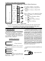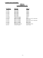
1
HMS Electronics
5935 Labath Avenue, Rohnert Park, California 94928
Tel: (707)584-8760 Fax: (707)584-7052
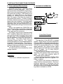
HS2-MPX Anode Rotator
'HIGH SPEED STARTER'
"R VERSION"
or
"R/Q VERSION"
***New***
500 Volt Output Capability
See Page 3 of manual
INSTALLATION AND SERVICE MANUAL
HS2-TP.PM 6
December 1996
CONTENTS
A.
B.
INSTALLATION PLANNING DATA ..................................... 2
INSTALLATION CONNECTIONS
1. POWER ..................................................................... 3
2. VERIFY LIGHTS ...................................................... 4
3. STATOR CONNECTIONS ...................................... 4-5
4. INPUTS AND OUTPUTS ........................................ 5-6
5. DIP SWITCH PROGRAMMING ............................. 6-8
6. FLUORO & SPOT FILM FUNCTIONS ................. 9
C. OUTLINE OF OPERATION ................................................... 10-12
D. TROUBLE SHOOTING (& Diagnostics) ............................. 11-15
E. TYPICAL SETUP CHART ..................................................... 17
E. PARTS LISTS ......................................................................... 18-27
F. SCHEMATIC DRAWINGS ..................................................... 28-
1
A. INSTALLATION PLANNING DATA
The system consists of a standard 19 inch
rack of electronics (approx. 35 pounds)
mounted in a NEMA enclosure (also 35
pounds).
Power Requirements:
208 to 240 VAC
50-60 Hz Single Phase
15 Amp "R" Version
30 Amp "R/Q" version
277 VAC ***[Not U.L. Approved]**
50-60 Hz Single Phase
12 Amp "R" Version
20 Amp "R/Q" Version
Enclosure Dimensions
Suitable for use on a circuit capable of
delivering not more than 5,000 rms Symmetrical Amperes, 240 volts maximum.
Mounting:
NEMA Type I enclosure
Total weight 70 pounds.
NOTE: The "R/Q" unit requires branch
circuit protection with maximum 30 Amp protector. The "R" unit requires branch circuit
protection with a maximum 20 Amp protector.
It is recommended that a multi-conductor cable
be used for interface connections. The interface wiring or cable must have a 600 Volt
insulation. Recommended wire size for interface 20 Gauge maximum.
The proper sequence of installation steps are
as follows.
1. Measure line voltages and connect
autotransformer taps.
2. Turn on power and verify lights OK.
3. Connect stators.
4. Connect inputs and outputs.
5. Program DIP switches.
6. Fluoro & Spot-Film Functions.
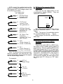
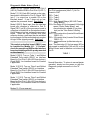
Enclosure mounting hole pattern
The proper manner to perform these steps
is explained in the following pages.
2
B. INSTALLATION CONNECTIONS
1. Power.
Refer to the main schematic
MAINS: Use maximum 10 Gauge wire or
minimum 12 gauge wire for the "R/Q" models.
Use maximum 10 Gauge wire or minimum 14
gauge wire for the "R" model.
Utilize the terminals provided in the connector
kit for connections of the mains to the circuit
breaker. In the event that solid wire is used, as
the connectors are intended for stranded wire,
the connectors must be soldered to the wire
before connection to the circuit breaker.
The incoming AC line goes directly to the
circuit breaker below the chassis. Connect the
ground wire to the ground lug provided, in the
bottom of the cabinet. Measure the incoming
voltage leg to leg. Select the proper line
matching taps on top of 1T1 (Autotransformer)
& 1T2 (low voltage transformer).
The taps are accessible by tipping the 19
inch rack assembly down. Please note that the
ground screw for the green grounding wire is
used as a stop for the chassis. Once the taps
are connected, turn on power and measure for
one of the following:
5944 AUTO
TRANSFORMER
1.1 440 Volts High Speed start voltage
Measure the 370 volts from tap 1 to the 370 Volt
tap (see HS2-MPX Schematic). If this voltage
is greater than 385 VAC change the input taps
to provide a lower output. Under no condition
may the starter be operated with the autotransformer output voltage greater than 385 VAC
from tap 1 to the 370 Volt tap. The 5 Volt tap
is intended for fine adjustment of the line input.
1.2 500 Volts High Speed start voltage
Measure the 416 volts from tap 1 to 12 on the
autotransformer (see HS2-MPX Schematic).
If this voltage is greater than 420 VAC change
the input taps to provide a lower output. Under
no condition may the starter be operated with
the autotransformer output voltage greater than
420 VAC from tap 1 to the 416 Volt tap. The 5
Volt tap is intended for fine adjustment of the
line input.
3
April '97
2. Verify Lights
KAUX relay is under program control and is
intended to be interfaced so as to provide
separate low speed and high speed interlock to
the generator. This is easily accomplished by
connecting one leg of the current interlock (KaKp [CB511]) to the common of Kaux and then
the low speed interlock connected to the normally closed contact. The high speed interlock
would of course be wired to the normally open
contact.
With software version 3.x and up, Kaux
status is determined by SW1-1 on CB515. If
SW1-1 is on, Kaux is programmed on during a
brake cycle to allow for interface with generators requiring a tube change inhibit signal. With
SW1-1 OFF, Kaux is programmed on with high
speed rotation command (requires a High Speed
start reason other than Fl=High Speed to be on.
When you apply the power (after the proper
taps have been selected), the relays are sequenced. The order of sequence is:
1. Tube 1 [ K1 on CB511]
2. Tube 2 [ K2 on CB511]
3. Tube 3 [ K3 on CB511]
4. Low speed start [ K1 on CB513]
5. Low speed run [ K2 on CB513] &
[ K6 on CB511]
6. High speed start [ K5 & K6 and K3
on CB513]
7. High speed run [ K5 & K6 and K4
on CB513] & [ K6 on CB511]
On the light bar, CB515, the "+5" status LED
should be on and the "OK" status LED should be
flashing at one second intervals.
On the Inverter Driver Board (CB512) all
threeLED’s should beONand of equal brightness.
On the mother board (CB517)LED 1 &
LED 2should beOFF. If any of these lights is
not correct, something is wrong. Consult
the trouble-shooting section.
If all the lights are OK, proceed with the
installation connections.
Installation Connections
3. Stators
On the edge of the tube selection board
(CB 511) are three terminal blocks for the
stator connections. Verify the /Q or /R in the
model number of the starter to be used with a
"Q" or "R" type stator. For R/Q models verify
that the program jumpers (dip switches version -6 and up) on interface board (CB515)
match the "Q" or "R" type at the appropriate
tube selection site. R/Q models are shipped
with tubes 1 & 3 selected as "Q" stators and
tube 2 selected as an "R" stator. WARNING!
If a "Q" stator is connected and an "R" type is
programed, damage to the starter may result.
Refer to the interface drawing for jumper/
switch identification. [ Tube1, jumper/switch
right of D10: Tube 2, jumper/switch right of
D11: Tube 3, jumper/switch right of D12].
The Serv-Norm (Service-Normal) jumper
is provided on the interface board in order to
achieve continuous rotation during calibration.
In the SERV position if a low speed start is
given, then the tube is held in low speed until a
tube change or high speed is selected. If a high
speed signal is given, then the tube is rotated in
high speed until a tube change is selected.
When the jumper is removed then the tube
brakes and returns to normal operation.
4
B. INSTALLATION CONNECTIONS CONTINUED
CB-511-6
Typical Stator Resistance
(Wht)
C3
(Blk)
P3
(Grn or Red)
A3
C-P (White to Black) 15-20 Ohms
P-A (Black to Green or Red) 50-70
Ohms
C-A (White to Green or Red) 40-50
Ohms
Typical stator
Designations
U9
(Wht)
C2
U7
(Blk)
P2
U8
(Grn or Red)
A2
H9
O9
(Wht)
C1
H7
O7
(Blk)
P1
H8
O8
(Grn or Red)
A1
Tube3
Red or Green is now commonly being
used for the phase or shifted winding.
P = Black
(Principal Winding or Main)
A = Green or Red
(Auxilary or Phase Shifted)
C = White
(Common winding)
Tube 2
Tube 1
Please note:
Any Green wire with a yellow stripe is not a stator wire but a ground wire!
Incorrect connections of the stator will be detected in high speed
and will cause a high speed fault condition!
4. Inputs and Outputs
All inputs go into opto-isolators. The standard manner of making a command is to apply
12 to 24 volts AC or DC with the jumpers
installed above the 2 watt resistor associated
with the input { or 110 volts AC or DC by
removing the jumper above the 2 watt resistor
associated with the input}. It is preferable to
use the power from the generator to supply
these command signals. If your generator or
spot filmer cannot, then +24 VDC and ground
are available on J2 pins. Using this internal DC
will expose the ground of the electronics rack
to the outside environment and may introduce
noise into the system. If you use the internal
24VDC, it may be necessary to use shielded
cables between the starter and generator. Tie
the shield to chassis ground.
All generator logic inputs and outputs are
made to the J2 connector on the front edge of
the interface board (CB515). Using the connector and pins supplied, make a harness.
The interface outputs of this starter are all
relay contacts. They will carry a maximun 3
amps at 30 VDC or 250 VAC.
Installation Connections
J2- Terminals
21
X-Ray Interlock.
22
Contacts close when rotor is up to
speed and exposures are then permitted.
19
18
A typical input (somewhat simplified) is as
follows:
Kaux
Logic Level to CPU
20
Kaux programmed on with high speed
orientation. Software version 3.x and
CB515 SW1-1 OFF.
5
If DC is used, the positive lead must be
applied to the proper terminal to turn on the
opto-isolator LED. If AC voltage is used, it will
be rectified by the diode.
The inputs are:
J2- terminals
3 ST(Rad Prep)
[Usually from
2 handswitch]
5
4
7
6
9
8
5. DIP Switch Programming CB514
(processor)
There are two dip switch banks on the
microprocessor boards (CB514). They are
called SW1 and SW2.
SW2
FL(Fluoro)
[usually from
the generator]
SW1
HS(High Speed)
[usually from tube
protector in
generator]
SW1. This group of eight switches controls
the accelerate/brake times for
Tube 1 and
Tube 2.
SW2. This group of four switches controls
the accelerate/brake time for
Tube 3.
Refer to page 6 for the SW1 and SW2 time
table chart.
SF (Spot Film
Transfer)
[Usually "RL"from
spot filmer]
11 TC2
(Tube change 2)
10 [Tube 3 selected]
Dip Switch Programming CB515
(Interface)
There is one switch (SW1) on CB515 interface which is set to enable various options of
programming. There is a switch (SW2) for the
R/Q model to select the "R" or "Q" stator type,
a switch (SW3) to program which flouro tubes
will be held for minutes instead of seconds in
high speed. Extended hold for high speed is
made by switch selection. For the Fluoro
functions to be enabled, the tube rotation must
be started with "FL" (Fluoro) or "SF" (SpotFilm).
13 TC1
(Tube Change 1)
12 [Tube 2 selected]
Note: To minimize the wires required from
starter to generator, you may link all of the
return lines together, assuming all the signals
use the same voltage source.
For example:
3
ST [+]
(Rad Prep)
2
5
FL [+]
(Fluoro)
4
7
6
HS [+]
(High Speed)
Common
6
B. INSTALLATION CONNECTIONS CONTINUED
SW1-1 [On]
K-aux on during brake.
1
CB514-SW2
2
3
4
Delay
1
2
3
4
Off Off Off Off
On Off Off Off
Off On Off Off
On On Off Off
0.60
0.65
0.70
0.80
5
6
7
Off Off
On Off
Off On
On Off
On Off
On Off
0.85 Sec
0.90 Sec
0.95 Sec
SW1-4 [On]
HS=High Speed Start (HS by itself will
initiate High Speed Rotation)
8
9
10
11
On On On Off
Off Off Off On
On Off Off On
Off On Off On
1.00 Sec
1.05 Sec
1.10 Sec
1.20 Sec
SW1-5&6 [On]
Control high speed hold time
(see High Speed Hold Table)
12 On On Off
13 Off Off On
14 On Off On
On
On
On
1.30 Sec
1.40 Sec
1.50 Sec
SW1-7* [On]
Forces a .75 second delay while in HIGH
SPEED HOLD & before X-Ray when a
new start is commanded (removes inter
lock for .75S). When tube 3 is not used,
insert the Diagnostic Jumper 'D2' on
CB514 and the Delay Table will become
active thereby making the delay adjustable.
15 Off
16 On
On
On
1.60 Sec
1.70 Sec
SW1-1 [OFF]
K-aux on with high speed command.
SW1-2 [On]
No DC Brake.
SW1-3 [On]
Hold cancel (generator has hold for low
speed fluoro hold time).
On
On
On
On
Sec
Sec
Sec
Sec
Delay Table
Selected by Diagnostic Jumper 'D2' on
CB514 and SW1-7 on CB515
SW1-8 [On]
Forces high speed FLUORO
(FL input will initiate High Speed
Rotation and Hold will be enabled, Kaux
relay will remain OFF until a normal High
Speed command).
SW1-5
SW1-6
Hold
Hold *D3
*Extend
Extend *D3
CB515
CB515
CB515
CB514
CB515
CB514
1
Off
Off
0 Sec
10 Sec
2 Min
4 Min
2
On
Off
20 Sec
40 Sec
3 Min
6 MIn
3
Off
On
35 Sec
70 Sec
5 Min
10 Min
4
On
ON
50 Sec
100 Sec
8 MIn
16 Min
High Speed hold table
Notes:
*Extended High Speed Hold: CB515 extended hold switch (SW3) enables extended hold times dependent on tube selection. This is a Fluoro function.
*D3 Install the Diagnostic Jumper D3 on CB514 to obtain the 'D3' hold times
listed in the high speed hold table.
7
April 22,1997
DIP Switch Programming Microprocessor
Select the combination which is appropriate for your tube. SW1-1 through SW1-4 are for
tube 1, and SW1-5 through SW1-8 are for tube 2 & SW2-1 through SW2-4 are for tube 3.
To avoid overheating the housing, it is advisable to choose the shortest time combination
which fully accelerates the anode.
combination
lo acc.
time
hi acc.
time
lo-hi acc.
time
TUBE1 SW11 2 3
4
TUBE2 SW1TUBE3 SW25 6 7
8 1 2 3 4
1
0.8
.80
.7
off off off off
off off off off
off off off off
2
0.9
.9
.75
on off off off
on off off off
on off off off
3
1.0
1.0
.8
off on off off
off on off off
off on off off
4
1.2
1.2
.85
on on off off
on on off off
on on off off
5
1.3
1.3
.9
off off on off
off off on off
off off on off
6
1.5
1.5
1.0
on off on off
on off on off
on off on off
7
1.6
1.7
1.2
off on on off
off on on off
off on on off
8
1.8
1.8
1.35
on on on off
on on on off
on on on off
9
2.0
2.0
1.5
off off off on
off off off on
off off off on
10
2.5
2.5
1.8
on off off on
on off off on
on off off on
11
3.0
3.0
2.2
off on off on
off on off on
off on off on
12
3.2
3.2
2.4
on on off on
on on off on
on on off on
13
3.5
3.5
2.6
off off on on
off off on on
off off on on
14
4.0
4.2
3.1
on off on on
on off on on
on off on on
15
4.5
4.8
3.2
off on on on
off on on on
off on on on
16
5.0
5.2
3.5
on on on on
on on on on
on on on on
Start-Run Delay Times
8
B. INSTALLATION CONNECTIONS CONTINUED
6. Fluoro and Spot Film functions
C. OUTLINE OF OPERATION
Energizing the Fluoro or Spot Film inputs
enables a 2 minute hold cycle. That is, the
starter maintains LOW SPEED continuous rotation for two minutes following any Fluoro (SF)
low speed start condition. If this feature is not
desired, set switch SW1-3 on the interface
board to on. Another function of the FluoroSpot Film inputs is that they also enable the
high speed hold function. If rotation is begun
by either of these inputs then an optional high
speed hold time is enabled. If the high speed
hold time is set to zero (see Dip Switch Programming) then the high speed hold is cancelled. See the table on Page 6 for the hold time
options.
When in low speed hold, 3300 RPM, only
70% of the start time is required to obtain high
speed. This reduces the time delay between
Fluoro and spot film exposures.
The "Delay" function set by interface board
SW1-7 enables a delay before exposure of .75
seconds when a start command is given while
in a hold cycle. This is available in the event
that the generator or spot film device has no
built-in delay. This delay should allow for
necessary filament heat-up. This function
causes high speed run to be released and then
re-applied .75 seconds later. This action removes the current through the current sensing
relays and exposure permission is lost, during
the .75 second delay on exposure.
All hold functions are cancelled by a tube
change selection.
Power Block Diagram
The operation of the HS2-MPX is straight
forward. There are two AC power supplies 50/
60Hz and 180Hz. If low speed stator operation
is commanded, the 50/60Hz source will supply
220 VAC for start and 60 VAC for run. For high
speed operation, the 180Hz inverter chops
440 VDC (start) and 100 VDC (run) into 180Hz
AC, for “R” stator. For “Q” stator 350VDC
(start) and 80VDC (run).
The start and run voltages are directed into
the phase shift capacitor and current sensing
relays. By output relay selection, either of
three tubes may be selected.
During high speed braking, 50/60Hz AC is
applied to the tube, then DC is applied if DC
brake is enabled.
The control of all functions is achieved by
relays driven by a microprocessor. The microprocessor responds to commands from the
generator. With its memory and the input data,
all functions are monitored and current operating status is indicated on LED’S.
Calibration:
There are no calibration adjustments.
9
C. Outline of Operation (Continued)
Refer to the over all schematic
In low speed operation, 220 VAC or 60 VAC
is taken directly from transformer 1T1, passed
through relay K5 to [I] and [K] terminals. [K] is
the principal winding source. [I] is connected to
1C1 and 1C2 which are the phase shift capacitors. Terminal [J] is the auxiliary winding
source.
During acceleration time, K6[CB511] (the
run relay) is de-energized. The closed contacts disable the current transformers from
coupling the current to the sensing circuits.
The AC passes from [J] and [K] directly to
whichever tube is selected. For run, K6[CB511]
will open its contacts. The AC will now pass
through the current sensing circuits and the
current sensing will turn on the interlock relay.
These current sensing circuits are used to
signal to the generator that exposures are
permitted.
For high speed operation, either 370 VAC
or 72 VAC is directed to 1CR1, (300 VAC or 55
VAC) for “Q” stator. The output on terminals [F]
and [G] is a DC Voltage which is applied to the
inverter.
On the inverter Driver Board (CB512), the
two sets of opto-isolators are driven by the
microprocessor port D bits 5 and 6. The timing
consists of 5.68 millisecond intervals and is set
by internal programing (180Hz). These signals are coupled through the opto- isolators to
the bases of four driver transistors. The driver
transistors have isolated power supplies as
required for operating the inverter transistors.
The Driver and Inverter transistors are set
up so that when Inverter transistors Q1 and Q2
are on, Q3 and Q4 are off. With Q1 on, the DC
[F] is connected up to [M] and Q2 connects the
DC [G] to [L]. When the drive changes polarity,
Q1 and Q2 turn off and Q3 and Q4 turn on. This
will apply the opposite polarity DC to [L] and
[M].
[L] and [M] are the square wave 180Hz AC
source. This 180Hz AC is applied via K5 relay
contacts (now energized) to [K] and through
1C2 to [J].
Input data, from the generator, is isolated
by opto-isolators to protect the microprocessor
from external noise. The conditions of the
inputs is shown on status LED’S. The data is
passed through input ports to the microprocessor and software routine. Output ports control
Driver transistors and operating status LED’s.
The solid state relay 1SS1 is opened each time
any power relay is actuated. This removes
incoming power momentarily and prevents
contact arcing.
CURRENT DETECTION during a start cycle is
provided by the current circuit located on the
mother board (T1, Z2, Z3, R5, Q2). On powerup the current window signal is checked for a
high level (+5V) [unless the service jumper is
installed]. During a start cycle the current
window is checked for active low, 50/60 or 180
HZ pulses, indicating that current is flowing.
With this signal CORRECT, a run cycle will be
enabled. If the signal is not correct then the
start cycle will be suspended and the program
will wait for all start reasons to be released.
After start commands are removed, then the
tube selection relays will be cycled quickly to
give a 'software reset' indication. This safety
feature will detect faulty start conditions caused
by defective relays, blown fuses, bad connections, faulty relay driver or a defect in the
microprocessor board.
DC BRAKE is achieved by applying High Speed
run signals to appropriate relays ,and the microprocessor turns on 1/2 of the inverter during
the brake period. This applies about 60VDC to
the stator "Principal" or "Main" winding.
10
.
Review---Current Window
RESET During Operation
The current in the common of the stator is
actively monitored during both low and high
speed starts. In low speed, the signal is looked
at for a low each time the line crosses through
zero. Since the sum of the main and shifted
currents should not be a low value, the "Current Window" signal should be low at line
crossing through zero. In high speed, the
"Current Window" signal is checked for a low
each time that the inverter is switched. Again,
the sum of the main and shifted currents should
not be a low value when the inverter is being
switched. In high speed the impedance matching of the main and shifted winding is more
critical than in low speed. The windings must
be connected properly or the "Current Window" signal will become distorted due to improper phase of the two currents (main and
shifted). Therefore, the "Current Window" will
not always detect a fault in low speed, but will
detect improper connections in high speed.
The stator connections when connected backward, will cause the tube to rotate backward in
low speed and the tube will come up to proper
speed--no problem. However, in high speed
the tube will not come up to speed when trying
to rotate backward.
HARDWARE RESET: This reset is generally caused by arcing of relay contacts during
a start, run or brake sequence. This is most
likely to occur in the event that the solid state
relay is shorted or defective in some way.
The unit will act like it was just turned on and all
of the relays will be cycled.
SOFTWARE RESET: This reset is generally caused by a current phase error in the
common of the supply to the stator. If this is the
reset condition, then temporarily moving the
service-normal jumper on the interface board
to the service position will disable this software
safety and a normal start-run sequence will
complete. The usual cause for this condition is
that there is a problem with the connections to
the x-ray tube stator windings.
STATOR VOLTAGES The following voltages +-10% should be the typical output voltages of
the starter as measured Common to Principle (C-P).
Q STATOR
Q STATOR
START
340 VAC 180HZ
220 VAC 60HZ
RUN
60 VAC 180HZ
52 VAC 60HZ
BRAKE
220 VAC BRAKE1, 50VDC BRAKE2
50 VDC BRAKE
R STATOR
R STATOR
440 VAC 180HZ
220 VAC 60 HZ
100 VAC 180HZ
54 VAC 60HZ
220 VAC BRAKE1, 60VDC BRAKE2
60VDC BRAKE
**With tap 12 on the autotransformer selected**
R STATOR ~500 VAC 180HZ 100 VAC 180HZ 220 VAC BRAKE1, 60VDC BRAKE2
11
September 96
D. TROUBLE SHOOTING
Jan 8, 1992
Use Diagnostic 0, Mode 2 to run the driver
board and test both driver and inverter boards.
(see page 13)
Failure of Inverter (CB510):
Using an Ohmmeter, measure the resistance of the four power transistors. They
should all be similar in resistance checks. Generally, the Inverter transistors will short base to
collector. If any power transistor block checks
shorted, replace it. Also, since the transistor(s)
likely would have shorted base-collector, this
would have burned out the base resistor and it
will need replacing. In the event of a failure of
the inverter do a dynamic check of the Driver
Board (CB512).
If repeat failures occur:
1. Check that there is no possibility of the stator
wires shorting to each other or to ground as one
single arc will instantly destroy the inverter.
2. Check the two current transformers on the
Tube Select & Safety board (CB511) to insure
that they are not arcing from primary to secondary. They should have infinite resistance from
primary to secondary and are insulated to withstand 2000V. After an arc, there is usually
some carbon created and some resistance will
be able to be measured.
3. An intermittent drive signal from the driver
board may cause failures especially for “Q”
stators. See 'Driver Board Dynamic Test' to
verify proper driver board operation.
4. Check the snubber networks for open 15
Ohm resistors or open .68 microfarad capacitors.
Inverter Failure Symptoms
1.
2.
3.
4.
High speed is commended.
HS relays and start relay pulls.
No high speed inverter signal to tube stator.
The starter goes to stand by mode ~ .3
seconds into start.
5. At release of high speed start, AC BRAKE
is applied (V3.5 & up software), and then
the relays are sequenced as if power had
just turned on. This was caused by the
current window not being active 180 HZ,
i.e. no power to stator or an improper phase
angle was detected in the common lead.
6. The storage capacitor will probably be
charged to about 460 VDC during the HS
start cycle if the cause is failure of the
inverter section.
Driver Board Static Test (CB512)
Feel the 10 watt resistors on the board. All
resistors should be cool in standby operation
(inverter not running). If any are HOT then the
associated driver transistor or its associated
opto-isolator are defective and need replacing.
Driver Board Dynamic Test (CB512)
1. Remove the 'Power Relay Board'
and the 'Inverter Board'.
3. Put the 'Driver Board' on the
Extender Card.
4. Turn the unit on.
5. After a minute or two, all four of
the 10 watt resistors should be
cold.
6. Use Diagnostic 0, Mode 2 to run
the inverter & driver for dynamic
testing. (see page 13)
7. On the Driver Board, Successively
jumper the 510 ohm 1/4Watt resis
tor at the output of each of the four
driver stages and verify that the
appropriate 10 watt resistor begins
to heat up. (jumpering the 510
ohm resistor provides a load for the
driver stage). You may want to
verify about a 4+ VDC drop across
the 10 watt resistor with the 510
ohm resistor jumpered.
Test Notes:
Jumper R2 , R1 gets hot.
Jumper R7, R6 gets hot.
Jumper R11, R10 gets hot.
Jumper R16, R17 gets hot.
12
November 21, 1996
D. TROUBLE SHOOTING CONTINUED
CPU Board (CB514) Cont'd
Power Relay Board (CB513)
Since the relays are all sequenced on and
off immediately following the power being turned
on, if any relay or relay contacts are suspected
just turn power off then after 2 seconds turn
power back on and watch for the relay to come
on, and its associated contacts to change position. To manually control the relays, use Diagnostic 0, Mode 0 (see page 13 and Table 1 on
page 14).
Safety and Tube Select Board ( CB511)
In the event of no rotor interlock with normal
anode rotation check for the following:
1. Insure that relay K6 comes in with RUN as
its contacts have to open to allow for current to
pass through the current sensing circuits. Repair sensing circuits as necessary. To manually control the relays on this board use Diagnostic 0, Mode 0 (see page 13 and Table 1 on
page 14)
Verify that the "OK" status LED on CB515
flashes at 1 second intervals. If it does not,
check for the presence of the 50/60Hz signals
from CB515. If the 50/60Hz signals are present
and the 1 Hz signal is not flashing then the CPU
is likely not running.
The microprocessor board has its own
power up reset and watchdog circuit. Verify
that power up reset is high. If the reset remains
low repair the reset circuit U1. If reset performs
properly, check for the two 50/60 Hz pulses to
U10 (CA1 pin 40, and CB1 pin 18). The reset
chip "DS1232" will maintain a low at the reset
output if the 5Volt supply falls below 4.65Volts.
*See pages 13-14 for Diagnostic Notes
Current Safety Mother board
The LED on the mother board should come
on during a start cycle (high current) and will be
off during standby, (no current flowing). The
service position of the jumper on the interface
board allows software to disregard the current
window signal. This allows for easier trouble
shooting.
Microprocessor Board CB514
In the event of a microprocessor board
malfunction, the board should be replaced.
The following diagram for the light bar is given
for your convenience.
10 +5 Volts
9 N/C
8 Autotransformer
7 Inverter Drive (CB512)
6 Inverter Drive (CB512)
5 Run (K6-CB511; K2 or K4-CB513)
4 High Speed (K5 & K6-CB513)
3 Tube 3 (K3-CB511)
2 Tube 2 (K2-CB511)
1 Tube 1 (K1-CB511)
Interface Board (CB515)
1. Check the 24 volt unregulated and 5 volt
regulated and verify them as being OK.
2. Verify, using the Light Bar as an indicator
that the corresponding light illuminates with
the appropriate opto-isolator using the J2
connector.
3. Verify the presence of the 50/60Hz signals
from U10 in the event that the CPU seems
dead as all outputs timing to the relays is
derived from the two 50/60Hz signals.
Note: The opto-isolators are open collector
output. This means that you can use a
jumper to bring the output low. As you bring
an opto-isolator output low, the output of
the buffer chip U8 should go low and the
appropriate LED on the light bar should
turn on.
4. Neither buffer chip should be hot. U7 buffer
is only read at turn on and after release of
a start. If You feel that the two chips are
conflicting, remove U7, and try them both
in the U8 position, then as you ground
each input, each output should go low.
13
September 21, 1996
Diagnostic Mode Notes for CPU (CB514):
Version 4.x software and up now does a
checksum test on the eprom and a ram test. If
the Eprom checksum fails, the Light bar LED 9
will blink. If Ram test fails, the Light bar LED 9
will blink and the solid state relay will be on
(LED 8 of the light bar). Starter operation is
disabled.
Version 4.1 Adds a test of current window
signal during the relay cycle test. If the current
window signal is low, fast blink of 'OK' LED on
interface board and LED9 of procesor board.
Starter operation is disabled.
Version 4.1 Adds a delay between turning on
relays during power-up to prevent welding of
contacts should the solid state relay be shorted.
Version 4.2 keeps software compatible with
older processor boards (watchdog circuit).
Diagnostic 1 (Switch 2 test):
Move the diagnostic Jumper from the 'N' to
the '1' position on the processor board, turn
on power, SW2 test is enabled.
SW2 Test: As each switch of SW2 is turned on
or off, the corresponding LED (1-4) on the light
bar should turn on and off. LED 1 of the light
bar is nearest SW1 (bottom LED) If any of the
four LED's do not follow the switch settings
then the processor board is likely defective.
Diagnostic Modes SW2 on Processor Board:
(See Table 1 for utilization of these switches.)
SW2-> 1234
Mode 0 [0000]: Each SW1 switch on the processor board is reflected to Port D. Port D bits
are indicated by the light bar. If all 8 LED's on
the light bar do not reflect the status of SW1
switches, the processor board is likely defective. See Note1
Note: On older versions of processor boards,
(CB514 Rev 4 and older), The starter will
appear inoperative with the checksum or Ram
check error! (LED9 on the processor board is
not driven)
Mode 1 [1000]: Reflect Current Window signal
to Port D bit 7 (LED 4) , Short pin 'C' of the
processor board to signal ground, or short out
Q2 on Mother board to 'simulate' level change
on PA7. LED 2 on the mother board should
light while the short is present.
HS2 Diagnostics
These diagnostics allow the service engineer
to check out and evaluate the interaction of the
processor board and interface board as well as
checking all port inputs and outputs of the
processor board.
Mode 2 [0100]: Run Inverter Timer (Port D bits
5 & 6) & turn on Kaux relay on interface board.
Inverter Driver and Inverter boards may be
installed for this test.
Entering Diagnostic Mode:
1. Turn off Power
2. Remove all boards from the starter except
for the processor and interface board
(CB514 and CB515). Put the processor
board on the extender card.
3. Record settings of SW1 and SW2 on Processor board.
4. Record settings of SW1, SW2 and if you
have 'RQ' starter, SW3 on Interface board.
5. Turn off all SW1 on processor board.
6. Diagnostic 0 (Modes 0-15):
Move the diagnostic Jumper from the 'N' to
the '0' position on the processor board, turn
on power. Diagnostics Modes 0-15 is enabled.
Mode 3 [1100]: Turn on OK LED on Interface
Board. Pin A on processor board should go
high.
Mode 4 [0010]: Turn on Kaux relay on Interface
Board. Pin 1 on processor board should go
high.
Mode 5 [1010]: Turn on Start relay (see LED1
on mother board). Pin D of processor board
should be set high. Power Relay Board may be
installed for this test.
Note1: These diagnostic modes will turn on the
relays corresponding to table 1 if the
appropriate boards are installed. Damage to
Starter could result if not careful!
14
September 21, 1996
Diagnostic Mode Notes (Cont.)
Mode 6 [0110]: Reflect IRQA to Port D bit 5
(LED 6), Reflect IRQB to Port D bit 6 (LED 7).
Mode 7 [1110]: Each SW1 switch on the interface board is reflected to Port D. Signal 'OE2'
(pin F ) is output low to enable U9 on the
interface board. If pin F does not go low,
replace the processor board. See Note1
Mode 8 [0001]: Each input from the interface
board opto couplers is reflected to Port D.
Signal 'OE1' (pin E) of the processor board is
output low to enable U8 on the interface board.
If pin E does not go low, replace the processor
board. Since the opto couplers are open
collector devices, each input can be activated
by shorting pin 4 of the associated opto coupler
to logic 0volts (signal ground). See Note1
*****************************************************
Tube select and safety board (CB511) may
be installed for Modes 9-11. If Q stator,
check the operation of SW2 on the interface
board and enabling of the Kr-q relay mounted
on the chassis.)
*****************************************************
Mode 9 [1001]: Turn on Tube 1, and Reflect
Extended Time switch (SW3-1 on Interface
Board) to Port D bit 3 (4th LED from bottom).
Check SW2-1 on Interface board for Q select
if applicable.
Mode 10 [0101]: Turn on Tube 2 and Reflect
Extended Time switch (SW3-2 on Interface
Board) to Port D bit 3 (4th LED from bottom).
Check SW2-2 on Interface board for Q select
if applicable.
Port D bit assignments (bits 0-7), bit 0 is
closest to SW1
PD0 = Tube 1
PD1 = Tube 2
PD2 = Tube 3
PD3 = High Speed Relays (K5 & K6 Power
Relay Board)
PD4 = Run Relay (K2 for low speed, K4 for high
speed, Power Relay Board), and
current detection enable (X-ray Inter
lock) on the Tube Select & Safety
board.
PD5 = 1/2 inverter drive (Inverter Driver Board,
CB512-15)
PD6 = 1/2 inverter drive (Inverter Driver Board,
CB512-13)
PD7 = autotransformer (solid state relay enable)
Note: The start relay (K1 for low speed, K3 for
high speed is enabled by PA6 and Q1 on the
Mother Board and is therefore not driven by
Port D.
TABLE 1
Normal Operation: To return to normal starter
operation, simply turn the power on with the
Diagnostic jumper removed or in the "N"
position.
Mode 11 [1101]: Turn on Tube 3 and Reflect
Extended Time switch (SW3-3 on Interface
Board) to Port D bit 3 (4th LED from bottom).
Check SW2-3 on Interface board for Q select
if applicable.
Modes 12-15 are reserved.
*********************************************************************************************************
15
D. TROUBLE SHOOTING CONTINUED
General
The starter can be partially checked out without the microprocessor board installed. This
should only be done if necessary to verify that everything else is OK. With the CPU board
removed, make appropriate jumpers to ground on each of the relay drive outputs, in order to
activate each relay in turn.
When power is first applied each of the relays are turned on in sequence. This is a simple
routine which is intended to give an audio or visual that the microprocessor is running and
controlling the relays.
E. TYPICAL SETUP CHART
SW1-
1
2
3
4
5
6
7
8
Fischer
1
X
0
0
X
X
X
0*
G.E.
1
X
1
0
X
X
X
X*
Raytheon
1
X
1
0
X
X
X
X*
Shimadzu
0
X
0
1
X
X
X
X*
0=OFF
X=DON'T CARE
1=ON
* May be used for Spot-Film Camera input when High Speed is desired.
Typical Setup Table CB515 Interface
Test Fixture
A test fixture is available for ease of test and trouble shooting the HS2 starter. The test fixture
is plugged into the J2 connector on the interface and works both 24volt and 110volt AC
configurations. The fixture is available for $65.00.
16
E. PARTS LISTS
CB510-2
INVERTER BOARD
REFERENCE
DESCRIPT
PART NUMBER
510-2-C1
510-2-C2
510-2-C3
510-2-C4
510-2-EJ1
510-2-EJ2
510-2-PB1:Q2/Q3
510-2-PB2:Q1/Q4
510-2-R1
510-2-R10
510-2-R11
510-2-R12
510-2-R2
510-2-R3
510-2-R4
510-2-R5
510-2-R6
510-2-R7
510-2-R8
510-2-R9
510-2-W1
510-2-W2
510-2-W3
510-2-W4
CB510-2
CAPACITOR, METAL FILM
CAPACITOR, METAL FILM
CAPACITOR, METAL FILM
CAPACITOR, METAL FILM
EJECTOR LEVER
EJECTOR LEVER
POWER TRANSISTOR BLOCK
POWER TRANSISTOR BLOCK
RESISTOR, 5W
RESISTOR, 2W
RESISTOR, 2W
RESISTOR, 2W
RESISTOR, 5W
RESISTOR, 5W
RESISTOR, 5W
RESISTOR, 2W
RESISTOR, 2W
RESISTOR, 2W
RESISTOR, 2W
RESISTOR, 2W
2" WIRE, .110 PUSH-ON
2" WIRE, .110 PUSH-ON
2" WIRE, .110 PUSH-ON
2" WIRE, .110 PUSH-ON
CIRCUIT BOARD
.68MFD @ 400VDC MF/1.5
.68MFD @ 400VDC MF/1.5
.68MFD @ 400VDC MF/1.5
.68MFD @ 400VDC MF/1.5
S-202
S-202
CC50R1000K
CC50R1000K
15 OHM 5W WW
18 OHM 2W METAL
18 OHM 2W METAL
18 OHM 2W METAL
15 OHM 5W WW
15 OHM 5W WW
15 OHM 5W WW
56K OHM 2W METAL
56K OHM 2W METAL
56K OHM 2W METAL
56K OHM 2W METAL
18 OHM 2W METAL
2" WIRE, .110 PUSH-ON
2" WIRE, .110 PUSH-ON
2" WIRE, .110 PUSH-ON
2" WIRE, .110 PUSH-ON
CB510-PWB
17
E. PARTS LISTS CONTINUED:
CB511-6
TUBE SELECT & SAFETY
REFERENCE
DESCRIPT
PART_N
511-7-1 (LED)
511-7-2 (LED)
511-7-C1
511-7-C2
511-7-CR1
511-7-CR2
511-7-CR3
511-7-CR4
511-7-EJ1
511-7-K1
511-7-K2
511-7-K3
511-7-K4
511-7-K6
511-7-Q1
511-7-Q2
511-7-R1
511-7-R10
511-7-R2
511-7-R3
511-7-R4
511-7-R5
511-7-R6
511-7-R7
511-7-R8
511-7-R9
511-7-T1
511-7-T2
511-7-TB1
511-7-TB2
511-7-TB3
511-7-Z1
511-7-Z2
511-7-Z3
511-7-Z4
CB511-7
LED
LED
CAPACITOR, AE/A
CAPACITOR, AE/A
BRIDGE RECTIFIER
RECTIFIER
BRIDGE RECTIFIER
RECTIFIER
EJECTOR LEVER
RELAY, PC 24VDC
RELAY, PC 24VDC
RELAY, PC 24VDC
RELAY, PC 24VDC
RELAY, PC DPDT
TRANSISTOR, TO92
TRANSISTOR, TO92
RESISTOR, 1W
RESISTOR, 1/4W
RESISTOR, 1W
RESISTOR, 1/4W
RESISTOR, 1/4W
RESISTOR, 1/4W
RESISTOR, 1W
RESISTOR, 1W
RESISTOR, 1/4W
RESISTOR, 1/4W
TRANSFORMER, CURREN
TRANSFORMER, CURREN
TERMINAL BLOCK
TERMINAL BLOCK
TERMINAL BLOCK
ZENER DIODE, .4W 5.1V
ZENER DIODE, .4W 3.3V
ZENER DIODE, .4W 5.1V
ZENER DIODE, .4W 3.3V
CIRCUIT BOARD
3MM RED
3MM RED
22MFD @ 35VDC AE/A/.1
22MFD @ 35VDC AE/A/.1
1 AMP 200V DIP BRIDGE
1N4004
1 AMP 200V DIP BRIDGE
1N4004
S-202
G4W-2212P-US-TV5-HP24VDC
G4W-2212P-US-TV5-HP24VDC
G4W-2212P-US-TV5-HP24VDC
JW1AFEN-DC24V
HB2-DC24V
2N5307
2N5307
150 OHM 1W METAL
33K OHM
150 OHM 1W METAL
10K OHM
1K OHM
33K OHM
150 OHM 1W METAL
150 OHM 1W METAL
10K OHM
1K OHM
4548D
4548D
6PCV-03
6PCV-03
6PCV-03
1N759
1N746
1N759
1N746
CB511-PWB
18
E. PARTS LISTS CONTINUED:
CB512-5
DRIVER BOARD
REFERENCE
DESCRIPT
PART_N
512-5-C1
512-5-C2
512-5-C3
512-5-C4
512-5-C5
512-5-C6
512-5-C7
512-5-C8
512-5-D1
512-5-D10
512-5-D11
512-5-D12
512-5-D2
512-5-D3
512-5-D4
512-5-D5
512-5-D6
512-5-D7
512-5-D8
512-5-D9
512-5-EJ1
512-5-EJ2
512-5-LED1
512-5-LED2
512-5-LED3
512-5-Q1
512-5-Q1HS
512-5-Q2
512-5-Q2HS
512-5-Q3
512-5-Q3HS
512-5-Q4
512-5-Q4HS
512-5-R1
512-5-R10
512-5-R11
512-5-R12
512-5-R13
512-5-R14
512-5-R15
512-5-R16
512-5-R17
512-5-R18
512-5-R19
512-5-R2
512-5-R20
512-5-R21
512-5-R3
512-5-R4
CAPACITOR, AE/R
CAPACITOR, MYLAR
CAPACITOR, AE/R
CAPACITOR, MYLAR
CAPACITOR, AE/R
CAPACITOR, MYLAR
CAPACITOR, AE/R
CAPACITOR, MYLAR
RECTIFIER
RECTIFIER
DIODE
DIODE
RECTIFIER
RECTIFIER
RECTIFIER
RECTIFIER
RECTIFIER
RECTIFIER
RECTIFIER
RECTIFIER
EJECTOR LEVER
EJECTOR LEVER
LED
LED
LED
TRANSISTOR, TO220
HEAT SINK, TO220 (AAVID)
TRANSISTOR, TO220
HEAT SINK, TO220 (AAVID)
TRANSISTOR, TO220
HEAT SINK, TO220 (AAVID)
TRANSISTOR, TO220
HEAT SINK, TO220 (AAVID)
RESISTOR, 10W
RESISTOR, 1/4W
RESISTOR, 1/4W
RESISTOR, 10W
RESISTOR, 1/4W
RESISTOR, 1/4W
RESISTOR, 1/4W
RESISTOR, 1/4W
RESISTOR, 10W
RESISTOR, 1/4W
RESISTOR, 1/4W
RESISTOR, 1/4W
RESISTOR, 1/4W
RESISTOR, 1/4W
RESISTOR, 1/4W
RESISTOR, 1/4W
3300MFD @ 16VDC AE/R/.3
.01MFD @ 63VDC MF/.2
3300MFD @ 16VDC AE/R/.3
.01MFD @ 63VDC MF/.2
3300MFD @ 16VDC AE/R/.3
.01MFD @ 63VDC MF/.2
3300MFD @ 16VDC AE/R/.3
.01MFD @ 63VDC MF/.2
1N4004
1N4007
1N4148
1N4148
1N4004
1N4007
1N4004
1N4004
1N4007
1N4004
1N4004
1N4007
S-202
S-202
3MM RED
3MM RED
3MM RED
TIP106
5741-02-B00000
TIP106
5741-02-B00000
TIP106
5741-02-B00000
TIP106
5741-02-B00000
5 OHM 10W WW
330 OHM
510 OHM
5 OHM 10W WW
330 OHM
510 OHM
2K OHM
510 OHM
5 OHM 10W WW
330 OHM
510 OHM
510 OHM
2K OHM
2K OHM
2K OHM
510 OHM
19
E. PARTS LISTS CONTINUED:
512-5-R5
512-5-R6
512-5-R7
512-5-R8
512-5-R9
512-5-U1
512-5-U1S
512-5-U2
512-5-U2S
512-5-U3
512-5-U3S
512-5-U4
512-5-U4S
512-5-W1
512-5-W2
512-5-W3
CB512-5
RESISTOR, 1/4W
RESISTOR, 10W
RESISTOR, 1/4W
RESISTOR, 1/4W
RESISTOR, 1/4W
OPTO ISOLATOR, SCHMIDT
SOCKET, IC 6 PIN
OPTO ISOLATOR, SCHMIDT
SOCKET, IC 6 PIN
OPTO ISOLATOR, SCHMIDT
SOCKET, IC 6 PIN
OPTO ISOLATOR, SCHMIDT
SOCKET, IC 6 PIN
RESISTOR, ZERO OHM
RESISTOR, ZERO OHM
RESISTOR, ZERO OHM
CIRCUIT BOARD
20
330 OHM
5 OHM 10W WW
510 OHM
2K OHM
510 OHM
H11L1
6 PIN DIP /.3
H11L1
6 PIN DIP /.3
H11L1
6 PIN DIP /.3
H11L1
6 PIN DIP /.3
ZERO OHM RESISTOR
ZERO OHM RESISTOR
ZERO OHM RESISTOR
CB512-PWB
E. PARTS LISTS CONTINUED:
CB513-5
POWER RELAY BOARD
REFERENCE
DESCRIPT
PART_N
513-5-D1
513-5-D2
513-5-D3
513-5-D4
513-5-D5
513-5-D6
513-5-D7
513-5-D8
513-5-EJ1
513-5-EJ2
513-5-K1
513-5-K2
513-5-K3
513-5-K4
513-5-K5
513-5-K6
513-5-R1
CB513-5
RECTIFIER
RECTIFIER
RECTIFIER
RECTIFIER
RECTIFIER
RECTIFIER
RECTIFIER
RECTIFIER
EJECTOR LEVER
EJECTOR LEVER
RELAY, PC DPDT
RELAY, PC DPDT
RELAY, PC DPDT
RELAY, PC DPDT
RELAY, PC DPDT
RELAY, PC DPDT
RESISTOR 10K 10W
CIRCUIT BOARD
1N4004
1N4004
1N4004
1N4004
1N4004
1N4004
1N4004
1N4004
S-202
S-202
G4W-2212P-US-TV5-HP24VDC
RM 207 024
G4W-2212P-US-TV5-HP24VDC
RM 207 024
RM 207 024
RM 207 024
10K OHM 10W WW
CB513-PWB
21
E. PARTS LISTS CONTINUED:
CB514-6A
MICROPROCESSOR BOARD
Reference
Description
Part Number
514-5-C1
514-5-C2
514-5-C3
514-5-C4
514-5-C5
514-5-DS1
514-5-EJ1
514-5-EJ2
514-5-Q1
514-5-R1
514-5-R2
514-5-R3
514-5-R4
514-5-SW1
514-5-SW2
514-5-TPG
514-5-U1
514-5-U10
514-5-U2
514-5-U3
514-5-U4
514-5-U5
514-5-U5-S
514-5-U6
514-5-U7
514-5-U8
514-5-U9
514-5-U9-S
CB514-5
CAPACITOR, TANTALUM
CAPACITOR, TANTALUM
CAPACITOR, TANTALUM
CAPACITOR, MYLAR
CAPACITOR, MYLAR
LIGHT BAR
EJECTOR LEVER
EJECTOR LEVER
TRANSISTOR, TO92
RESISTOR, 1/4W
RESISTOR, 1/4W
RESISTOR, 1/4W
SIP RESISTOR
SWITCH, DIP
SWITCH, DIP
TEST POINT (WHITE)
IC, RESET
IC, I/O TIMER
IC, DECODER
IC, OSCILLATOR
IC, MICROPROCESSOR
IC, EPROM
SOCKET, IC 28 PIN
IC, RAM
IC, I/O TIMER
IC, OCTAL BUFFER
IC, OCTAL RELAY DRIVER
SOCKET, IC 18 PIN
CIRCUIT BOARD
1.0MFD @ 35VDC T/.1
1.0MFD @ 35VDC T/.1
1.0MFD @ 35VDC T/.1
.1MFD @ 63VDC M/.2
.01MFD @ 63VDC M/.2
10 SEG LIGHT BAR, RED
S-202
S-202
PN2222A
2K OHM
3K OHM
390 OHM
CTS770-101-391
8 POS. DIP SWITCH
4 POS. DIP SWITCH
151-201
DS1232
R6522
74HCT138
OSC 1.000 MHZ
R65(C)02
27C64 (PROGRAMMED)
28 PIN DIP /.6
2K X 8 (24 PIN)
R6522
74HCT541
ULN2803
18 PIN DIP /.3
CB514-PWB
22
E. PARTS LISTS CONTINUED:
CB515-6
INTERFACE BOARD
REFERENCE
DESCRIPT
PART_N
515-6-C1
515-6-C10
515-6-C11
515-6-C2
515-6-C3
515-6-C4
515-6-C5
515-6-C6
515-6-C7
515-6-C8
515-6-C9
515-6-CR14
515-6-D1
515-6-D10
515-6-D11
515-6-D12
515-6-D13
515-6-D14
515-6-D15
515-6-D16
515-6-D2
515-6-D3
515-6-D4
515-6-D5
515-6-D6
515-6-D7
515-6-D8
515-6-D9
515-6-EJ1
515-6-EJ2
515-6-J2A
515-6-J2B
515-6-J3
515-6-K1
515-6-LB1
515-6-P3
515-6-Q1
515-6-Q2
515-6-Q3
515-6-R1
515-6-R10
515-6-R11
515-6-R12
515-6-R13
515-6-R14
515-6-R15
515-6-R16
515-6-R17
515-6-R18
515-6-R19
515-6-R2
CAPACITOR, AE/R
CAPACITOR, MYLAR
CAPACITOR, TANTALUM
CAPACITOR, AE/R
CAPACITOR, AE/R
CAPACITOR, AE/R
CAPACITOR, AE/R
CAPACITOR, AE/R
CAPACITOR, TANTALUM
CAPACITOR, AE/R
CAPACITOR, AE/A
BRIDGE RECTIFIER
RECTIFIER
DIODE
DIODE
DIODE
DIODE
DIODE
DIODE
ZENER DIODE, .4W 5.1V
RECTIFIER
RECTIFIER
RECTIFIER
RECTIFIER
RECTIFIER
RECTIFIER
ZENER DIODE, .4W 5.1V
ZENER DIODE, .4W 5.1V
EJECTOR LEVER
EJECTOR LEVER
HEADER, 11 X 156
HEADER, 11 X 156
HEADER, 3 PIN
RELAY, PC 24VDC
LIGHT BAR
SHORTING PLUG
TRANSISTOR, TO220
TRANSISTOR, TO92
TRANSISTOR, TO92
RESISTOR, 2W
RESISTOR, 1/4W
RESISTOR, 1/4W
RESISTOR, 1/4W
RESISTOR, 2W
RESISTOR, 1/4W
RESISTOR, 1/4W
RESISTOR, 1/4W
RESISTOR, 2W
RESISTOR, 1/4W
RESISTOR, 1/4W
RESISTOR, 1/4W
33MFD @ 35VDC AE/R/.1
.01MFD @ 63VDC M/.2
1.0MFD @ 35VDC T/.1
33MFD @ 35VDC AE/R/.1
33MFD @ 35VDC AE/R/.1
33MFD @ 35VDC AE/R/.1
33MFD @ 35VDC AE/R/.1
33MFD @ 35VDC AE/R/.1
1.0MFD @ 35VDC T/.1
220MFD @ 50VDC AE/A/1.2
2200MFD @ 35VDC AE/A/1.6
2 AMP 200V RECT. BRIDGE
1N4004
1N4148
1N4148
1N4148
1N4148
1N4148
1N4148
1N751
1N4004
1N4004
1N4004
1N4004
1N4004
1N4004
1N751
1N751
S-202
S-202
09-60-1111 (MOLEX)
09-60-1111 (MOLEX)
3 PIN HEADER .1X3 ST.
JW1FEN-DC24V
10 SEG LIGHT BAR, RED
SHORTING PLUG, W/HANDLE
TIP106
PN2222A
PN2222A
5.6K OHM 2W METAL
510 OHM
1K OHM
1K OHM
5.6K OHM 2W METAL
510 OHM
1K OHM
1K OHM
5.6K OHM 2W METAL
510 OHM
1K OHM
510 OHM
23
E. PARTS LISTS CONTINUED:
515-6-R20
515-6-R21
515-6-R22
515-6-R23
515-6-R24
515-6-R25
515-6-R26
515-6-R27
515-6-R28
515-6-R29
515-6-R3
515-6-R30
515-6-R31
515-6-R32
515-6-R33
515-6-R34
515-6-R35
515-6-R36
515-6-R37
515-6-R38
515-6-R4
515-6-R5
515-6-R6
515-6-R7
515-6-R8
515-6-R9
515-6-RP1
515-6-SW1
515-6-SW2
515-6-SW3
515-6-U1
515-6-U10
515-6-U10S
515-6-U1S
515-6-U2
515-6-U2S
515-6-U3
515-6-U3S
515-6-U4
515-6-U4S
515-6-U5
515-6-U5S
515-6-U6
515-6-U6S
515-6-U7
515-6-U7S
515-6-U8
515-6-U8S
515-6-U9
515-6-U9S
CB515-5
RESISTOR, 1/4W
RESISTOR, 2W
RESISTOR, 1/4W
RESISTOR, 1/4W
RESISTOR, 1/4W
RESISTOR, 1/4W
RESISTOR, 1/4W
RESISTOR, 1/4W
RESISTOR, 1/4W
RESISTOR, 1/4W
RESISTOR, 1/4W
RESISTOR, 1/4W
RESISTOR, 1/4W
RESISTOR, 1/4W
RESISTOR, 1/4W
RESISTOR, 1/4W
RESISTOR, 1/4W
RESISTOR, 1/4W
RESISTOR, 1/4W
RESISTOR, 1/4W
RESISTOR, 1/4W
RESISTOR, 2W
RESISTOR, 1/4W
RESISTOR, 1/4W
RESISTOR, 1/4W
RESISTOR, 2W
SIP RESISTOR 390OHM
SWITCH, DIP
SWITCH, DIP
SWITCH, DIP
IC, OPTO ISOLATOR, SCHMID
IC, COMPARATOR
SOCKET, IC 8 PIN
SOCKET, IC 6 PIN
IC, OPTO ISOLATOR, SCHMID
SOCKET, IC 6 PIN
IC, OPTO ISOLATOR, SCHMID
SOCKET, IC 6 PIN
IC, OPTO ISOLATOR, SCHMID
SOCKET, IC 6 PIN
IC, OPTO ISOLATOR, SCHMID
SOCKET, IC 6 PIN
IC, OPTO ISOLATOR, SCHMID
SWITCH, DIP
IC, OCTAL BUFFER
SOCKET, IC 20 PIN
IC, OCTAL BUFFER
SOCKET, IC 20 PIN
IC, RELAY DRIVER
SOCKET, IC 8 PIN
CIRCUIT BOARD
24
1K OHM
5.6K OHM 2W METAL
510 OHM
1K OHM
1K OHM
10K OHM
10K OHM
10K OHM
10K OHM
10K OHM
1K OHM
10K OHM
10K OHM
10K OHM
47K OHM
47K OHM
10K OHM
1K OHM
200 OHM
390 OHM
1K OHM
5.6K OHM 2W METAL
510 OHM
1K OHM
1K OHM
5.6K OHM 2W METAL
770-101-R390
8 POS. DIP SWITCH
3 POS. DIP SWITCH
3 POS. DIP SWITCH
H11L1
LM393N
8 PIN DIP /.3
6 PIN DIP /.3
H11L1
6 PIN DIP /.3
H11L1
6 PIN DIP /.3
H11L1
6 PIN DIP /.3
H11L1
6 PIN DIP /.3
H11L1
6 POS. DIP SWITCH
74LS541
20 PIN DIP /.3
74LS541
20 PIN DIP /.3
75452N
8 PIN DIP /.3
CB515-PWB
E. PARTS LISTS CONTINUED:
CB517-5A
Mother Board
REFERENCE
DESCRIPT
PART_N
CB517-5
CB517-5-CR2
CB517-5-D1
CB517-5-J510
CB517-5-J511
CB517-5-J512
CB517-5-J513
CB517-5-J514
CB517-5-J515
CB517-5-LED1
CB517-5-LED2
CB517-5-Q1
CB517-5-Q2
CB517-5-R1
CB517-5-R10
CB517-5-R2
CB517-5-R3
CB517-5-R4
CB517-5-R5
CB517-5-R6
CB517-5-R7
CB517-5-R8
CB517-5-R9
CB517-5-T1
CB517-5-Z1
CB517-5-Z2
CB517-5-Z3
CIRCUIT BOARD
BRIDGE RECTIFIER
RECTIFIER
CONNECTOR, (CINCH)
CONNECTOR, (CINCH)
CONNECTOR, (CINCH)
CONNECTOR, (CINCH)
CONNECTOR, (CINCH)
CONNECTOR, (CINCH)
LED
LED
TRANSISTOR, TO92
TRANSISTOR, TO92
RESISTOR, 1/4W
RESISTOR, 10W
RESISTOR, 1/4W
RESISTOR, 1/4W
RESISTOR, 1/4W
RESISTOR, 1/4W
RESISTOR, 1/4W
RESISTOR, 2W
RESISTOR, 2W
RESISTOR, 2W
TRANSFORMER, CURRENT
VOLTAGE REG, 1 AMP 5V
ZENER DIODE, 1W 12V
ZENER DIODE, .4W 3.3V
CB517-PWB
1.5 AMP 200V (ROUND)
1N4004
50-22SN-5 22X156 SINGLE
50-22SN-5 22X156 SINGLE
50-22SN-5 22X156 SINGLE
50-44SN-1 22X156 DUAL
50-44SN-1 22X156 DUAL
50-44SN-1 22X156 DUAL
3MM RED
3MM RED
2N5307
PN2222A
10K OHM
15 OHM 10W WW
2K OHM
200 OHM
3K OHM
1K OHM
390 OHM
56K OHM 2W METAL
56K OHM 2W METAL
56K OHM 2W METAL
4548D
7805A
1N4742A
1N746
25
E. PARTS LISTS CONTINUED:
MISC. CHASSIS PARTS
HS2-MPX STARTER
REFERENCE
DESCRIPT
PART_N
CB510
CB511
CB512
CB513
CB514
CB515
CB517
EXTENDER
HS2-1C1
HS2-1C1A (Q)
HS2-1C2
HS2-1C2A (Q)
HS2-1C3
HS2-1C4 (Q)
HS2-1CR1
HS2-1F1
HS2-1F2
HS2-1F3
HS2-1F4
HS2-1F5
HS2-1F6
HS2-1FH1
HS2-1FH2
HS2-1FH3
HS2-1FH4
HS2-1FH5
HS2-1FH6
HS2-1K1
HS2-1R1 (Q)
HS2-1R2 (Q)
HS2-1R3 (Q)
HS2-1R4
HS2-1SS1
HS2-1T1
HS2-1T2
HS2-CB1 (Q)
HS2-CB1 (R)
HS2-LF1
INVERTER BOARD
TUBE SELECT BOARD
DRIVER BOARD
POWER RELAY BOARD
PROCESSOR BOARD
INVTERFACE BOARD
MOTHER BOARD
EXTENDER BOARD ASSY
AC CAP 25MFD @ 370
AC CAP 15MFD @ 440
AC CAP 6MFD @ 660
AC CAP 20MFD @ 440
AC CAP 3MFD @ 440
AE CAPACITOR
BRIDGE RECTIFIER
FUSE SLO-BLO
FUSE SLO-BLO
FUSE SLO-BLO
FUSE SLO-BLO
FUSE SLO-BLO
FUSE SLO-BLO
1-1/4 FUSE HOLDER
1-1/4 FUSE HOLDER
1-1/4 FUSE HOLDER
1-1/4 FUSE HOLDER
1-1/4 FUSE HOLDER
1-1/4 FUSE HOLDER
R/Q RELAY
RESISTOR
RESISTOR
RESISTOR
RESISTOR
SOLID STATE RELAY
AUTOTRANSFORMER
TRANSFORMER
CIRCUIT BREAKER
CIRCUIT BREAKER
LINE FILTER
CB510/W
CB511/W
CB512/W
CB513/W
CB514/W
CB515/W
CB517/W
CB4X5EXT
97F9006
97F9037
26F6623FA
97F9039
97F5437
36DX2000-450VDC
35MB120A (IR)
MDL 1/2
MDL 1/2
MDL 1-1/2
MDA 7
MDA 7
MDA 7
HKP
HKP
HKP
HKP
HKP
HKP
HG4-DC-24V
RH50-.2 OHM 1%
RH50-.2 OHM 1%
RH50-.2 OHM 1%
RH50-10 OHM 1%
SSR600240R55
5944
5251
ULP-11-1-66-203
ULP-11-1-66-103
20VB1
26
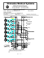
Shimadzu Medical Systems
National Technical Support
20101 S. Vermount Ave. Torrance, Ca. 90502
Tel. (800) 228-1429
Fax. (310) 217-0729
SERVICE BULLETIN
Model: HMS Starter and UD150B-30/L-30
Date: 10/19/98
Number: XR-980014
Title: HMS starter interface to the UD150B-30/L-30
Checked by:__________
Approved by:__________
Issued by: Gordon Bowller
======================================================================
UD150B-30/L-30
MOTHER-96 PCB
JS1
HS2 Interface PCB
J2
Install Jumpers for 15V
5V
U1
6
R1
2
4
1
R3
1K
C1
33
2
5.6K
D1
R2
B8
ST
Normal Speed
Rotation Start
2
5
R4
5V
1K
1N4004
510
3
*= no connections with
a RAD only system
4
**= no connections for
a one X-ray
tube systems
U2
6
R5
2
4
1
R7
1K
C2
33
5.6K
D2
R6
FL
5
R8
5V
1K
1N4004
510
U3
6
R9
2
4
1
R11
1K
C3
33
6
5.6K
D3
R10
5
R12
5V
1K
1N4004
510
A9
High Speed
Rotation Start
H2
HS
A1 B1 +15
7
+15V DC
U4
6
R13
2
4
1
C4
33
R15
1K
8
5.6K
D4
R14
5
R16
5V
5
1K
1N4004
510
x4 TERMINAL-96 PCB
SF
F
9
U5
6
R17
2
4
1
R19
1K
C5
33
L0
10
5.6K
D5
R18
5V
6
1K
1N4004
510
*
TC2
5
R20
*
11
SP1
*
U6
R21
2
4
1
C6
R23
1K
33
Tube 2 selected
B7
2M
A6
7
Normal Speed
Confirmation
20
B6
H7
High Speed
Confirmation
21
A15 B15
22
A5 B5
HON
1
A3 B3
+15V DC
12
5.6K
D6
R22
TC1
**
5
R24
1K
1N4004
510
+24V DC
13
15
Kaux
19
18
INTLK
GND
0V
CAUTION: DO NOT MIX +15V DC AND L100 POWER SUPPLIES
VERIFY ALL JUMPERS ON THE HMS INTERFACE PCB
Reference the connection diagrams in the UD150B-30/L-30 schematics
for MOTHER-96 (3/17) and TERMINAL-96 (5/6) PCB's.
page
of 1
1
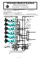
Shimadzu Medical Systems
National Technical Support
20101 S. Vermount Ave. Torrance, Ca. 90502
Tel. (800) 228-1429
Fax. (310) 217-0729
SERVICE BULLETIN
Model: HMS Starter and UD150L-F/RII
Date: 10/19/98
Number: XR-980015
Title: HMS starter interface to the UD150L-F/RII
Checked by:__________
Approved by:__________
Issued by: Gordon Bowller
======================================================================
UD150L-F or UD150L-RII
HS2 Interface PCB
5V
JS1
J2
Install Jumpers for 15V
XUD CONT-94 PCB
U1
6
R1
2
4
1
R3
1K
C1
33
2
5.6K
D1
R2
B8
ST
Normal Speed
Rotation Start
2
5
R4
5V
1K
1N4004
510
*= no connections
with
UD150L-RII
3
U2
6
R5
2
4
1
R7
1K
C2
33
4
5.6K
D2
R6
FL
**=no connections
for a one X-ray
tube systems
5
R8
5V
1K
1N4004
510
U3
6
R9
2
4
1
R11
1K
C3
33
6
5.6K
D3
R10
5
R12
5V
1K
1N4004
510
A9
High Speed
Rotation Start
H2
HS
A1 B1 +15
7
+15V DC
U4
6
R13
2
4
1
C4
33
R15
1K
8
5.6K
D4
R14
5
R16
5V
5
1K
1N4004
510
x1 XTV TERMINAL-94 PCB
SF
F
9
U5
6
R17
2
4
1
R19
1K
C5
33
L0
10
5.6K
D5
R18
5V
6
1K
1N4004
510
*
TC2
5
R20
*
11
SP1
*
U6
R21
2
4
1
C6
R23
1K
33
D6
Tube 2 selected
B7
2M
19
18
A6
7
Normal Speed
Confirmation
20
B6
H7
High Speed
Confirmation
21
A15 B15
22
A5 B5
HON
1
A3 B3
+15V DC
12
5.6K
R22
TC1
**
5
R24
1K
1N4004
510
+24V DC
13
15
Kaux
INTLK
GND
0V
CAUTION: DO NOT MIX +15V DC AND L100 POWER SUPPLIES
VERIFY ALL JUMPERS ON THE HMS INTERFACE PCB
Reference the connection diagrams in the UD150L-F/RII schematics
for XUD CONT-94 (7/13) and XTV TERMINAL-94 PCB's.
1
page
of 1