1
QUANTAR TECHNOLOGY
3300/2400 SERIES
SYSTEM INSTALLATION AND OPERATION
MANUAL
Copyright 1990-2013
Quantar Technology Incorporated
2620A Mission Street
Santa Cruz, CA 95060
Tel: 831-429-5227
FAX: 831-429-5131
www.quantar.com
18 Nov 2013, Rev I
This page is intentionally blank
3300/2400 System Manual
page 2
18 Nov 2013, Rev I
TABLE OF CONTENTS
LIST OF FIGURES . . . . . . . . . . . . . . . . . . . . . . . . . . . . . . . . . . . . . . . . . . . . . . . . . . . . . . . . . . . . . . . . . . . page 5
GENERAL INFORMATION . . . . . . . . . . . . . . . . . . . . . . . . . . . . . . . . . . . . . . . . . . . . . . . . . . . . . . . . . . . page 9
SCOPE OF THIS MANUAL . . . . . . . . . . . . . . . . . . . . . . . . . . . . . . . . . . . . . . . . . . . . . . . . . . . . . page 9
GENERAL DESCRIPTION . . . . . . . . . . . . . . . . . . . . . . . . . . . . . . . . . . . . . . . . . . . . . . . . . . . . . . page 9
SECTION 1. SYSTEM INSTALLATION . . . . . . . . . . . . . . . . . . . . . . . . . . . . . . . . . . . . . . . . . . . . . . . .
SENSOR ASSEMBLY MOUNTING . . . . . . . . . . . . . . . . . . . . . . . . . . . . . . . . . . . . . . . . . . . . . .
MOUNTING OF ELECTRONICS MODULES . . . . . . . . . . . . . . . . . . . . . . . . . . . . . . . . . . . . . .
CONNECTING SENSOR TO PREAMP . . . . . . . . . . . . . . . . . . . . . . . . . . . . . . . . . . . . . . . . . . .
SYSTEM INTERCONNECTION DIAGRAMS . . . . . . . . . . . . . . . . . . . . . . . . . . . . . . .
SIGNAL LEADS . . . . . . . . . . . . . . . . . . . . . . . . . . . . . . . . . . . . . . . . . . . . . . . . . . . . . .
ORIENTATION OF SIGNAL LEADS: A, B, C, D . . . . . . . . . . . . . . . . . . . . . . . . . . . .
SIGNAL LEAD DECOUPLING . . . . . . . . . . . . . . . . . . . . . . . . . . . . . . . . . . . . . . . . . .
HV LEADS . . . . . . . . . . . . . . . . . . . . . . . . . . . . . . . . . . . . . . . . . . . . . . . . . . . . . . . . . .
VACUUM FEEDTHROUGHS . . . . . . . . . . . . . . . . . . . . . . . . . . . . . . . . . . . . . . . . . . . .
GROUNDING AND BYPASSING . . . . . . . . . . . . . . . . . . . . . . . . . . . . . . . . . . . . . . . .
HIGH VOLTAGE BIAS . . . . . . . . . . . . . . . . . . . . . . . . . . . . . . . . . . . . . . . . . . . . . . . . .
HIGH VOLTAGE DIVIDER NETWORK . . . . . . . . . . . . . . . . . . . . . . . . . . . . . . . . . . .
HV BIAS CONFIGURATIONS . . . . . . . . . . . . . . . . . . . . . . . . . . . . . . . . . . . . . . . . . . .
CONNECTING PREAMP TO POSITION ANALYZER . . . . . . . . . . . . . . . . . . . . . . . . . . . . . . .
CONNECTING POSITION ANALYZER TO EXTERNAL DEVICES . . . . . . . . . . . . . . . . . . . .
ANALOG X AND Y POSITION SIGNALS . . . . . . . . . . . . . . . . . . . . . . . . . . . . . . . . . .
Z AXIS . . . . . . . . . . . . . . . . . . . . . . . . . . . . . . . . . . . . . . . . . . . . . . . . . . . . . . . . . . . . .
STROBE . . . . . . . . . . . . . . . . . . . . . . . . . . . . . . . . . . . . . . . . . . . . . . . . . . . . . . . . . . . .
SUM . . . . . . . . . . . . . . . . . . . . . . . . . . . . . . . . . . . . . . . . . . . . . . . . . . . . . . . . . . . . . . .
BUSY . . . . . . . . . . . . . . . . . . . . . . . . . . . . . . . . . . . . . . . . . . . . . . . . . . . . . . . . . . . . . .
RATE . . . . . . . . . . . . . . . . . . . . . . . . . . . . . . . . . . . . . . . . . . . . . . . . . . . . . . . . . . . . . .
VETO GATE INPUT . . . . . . . . . . . . . . . . . . . . . . . . . . . . . . . . . . . . . . . . . . . . . . . . . . .
DIGITAL X AND Y POSITION SIGNALS . . . . . . . . . . . . . . . . . . . . . . . . . . . . . . . . . .
DIGITAL STROBE . . . . . . . . . . . . . . . . . . . . . . . . . . . . . . . . . . . . . . . . . . . . . . . . . . . .
REAR-PANEL SWITCHES . . . . . . . . . . . . . . . . . . . . . . . . . . . . . . . . . . . . . . . . . . . . . . . . . . . . .
Y-AXIS DIGITAL OUTPUT MODE SWITCH . . . . . . . . . . . . . . . . . . . . . . . . . . . . . . .
1-D/2-D DIGITAL MEMORY MAPPING CABLE SWITCH . . . . . . . . . . . . . . . . . . . .
page 11
page 11
page 11
page 14
page 14
page 14
page 15
page 15
page 15
page 15
page 18
page 19
page 19
page 23
page 24
page 24
page 24
page 25
page 25
page 25
page 25
page 26
page 26
page 26
page 26
page 28
page 28
page 28
SECTION 2. SYSTEM OPERATION . . . . . . . . . . . . . . . . . . . . . . . . . . . . . . . . . . . . . . . . . . . . . . . . . . .
INITIAL TURN-ON AND CHECKOUT . . . . . . . . . . . . . . . . . . . . . . . . . . . . . . . . . . . . . . . . . . .
SYSTEM SET-UP . . . . . . . . . . . . . . . . . . . . . . . . . . . . . . . . . . . . . . . . . . . . . . . . . . . . .
VACUUM PRESSURE . . . . . . . . . . . . . . . . . . . . . . . . . . . . . . . . . . . . . . . . . . . . . . . . .
PRELIMINARY HV CHECK . . . . . . . . . . . . . . . . . . . . . . . . . . . . . . . . . . . . . . . . . . . .
CONNECT XY MONITOR . . . . . . . . . . . . . . . . . . . . . . . . . . . . . . . . . . . . . . . . . . . . . .
HV TURN-ON . . . . . . . . . . . . . . . . . . . . . . . . . . . . . . . . . . . . . . . . . . . . . . . . . . . . . . . .
INITIAL OPERATION . . . . . . . . . . . . . . . . . . . . . . . . . . . . . . . . . . . . . . . . . . . . . . . . .
CHECKING NOISE LEVEL . . . . . . . . . . . . . . . . . . . . . . . . . . . . . . . . . . . . . . . . . . . . .
CHECKING SPATIAL RESOLUTION . . . . . . . . . . . . . . . . . . . . . . . . . . . . . . . . . . . . .
OPTIMIZING HV BIAS SETTINGS . . . . . . . . . . . . . . . . . . . . . . . . . . . . . . . . . . . . . . . . . . . . . .
METHOD 1. INPUT LEVEL METER . . . . . . . . . . . . . . . . . . . . . . . . . . . . . . . . . . . . .
METHOD 2. OSCILLOSCOPE . . . . . . . . . . . . . . . . . . . . . . . . . . . . . . . . . . . . . . . . . .
METHOD 3. EXTERNAL PULSE HEIGHT ANALYZER . . . . . . . . . . . . . . . . . . . . . .
METHOD 4. BUILT-IN DIGITAL PULSE HEIGHT ANALYZER . . . . . . . . . . . . . . . .
page 30
page 30
page 30
page 30
page 30
page 31
page 31
page 32
page 32
page 33
page 33
page 33
page 33
page 34
page 34
3300/2400 System Manual
page 3
18 Nov 2013, Rev I
METER FUNCTIONS . . . . . . . . . . . . . . . . . . . . . . . . . . . . . . . . . . . . . . . . . . . . . . . . . . . . . . . . .
COUNT RATE . . . . . . . . . . . . . . . . . . . . . . . . . . . . . . . . . . . . . . . . . . . . . . . . . . . . . . .
DEAD-TIME PERCENT . . . . . . . . . . . . . . . . . . . . . . . . . . . . . . . . . . . . . . . . . . . . . . . .
INPUT LEVEL . . . . . . . . . . . . . . . . . . . . . . . . . . . . . . . . . . . . . . . . . . . . . . . . . . . . . . .
EDGE GATING CONTROLS . . . . . . . . . . . . . . . . . . . . . . . . . . . . . . . . . . . . . . . . . . . . . . . . . . .
OPERATING CONSIDERATIONS . . . . . . . . . . . . . . . . . . . . . . . . . . . . . . . . . . . . . . . . . . . . . . .
COUNT RATE AND DEAD-TIME . . . . . . . . . . . . . . . . . . . . . . . . . . . . . . . . . . . . . . . .
SPATIAL RESOLUTION . . . . . . . . . . . . . . . . . . . . . . . . . . . . . . . . . . . . . . . . . . . . . . .
page 35
page 35
page 35
page 36
page 36
page 36
page 36
page 40
SECTION 3. DIAGNOSTICS AND TROUBLESHOOTING . . . . . . . . . . . . . . . . . . . . . . . . . . . . . . . . . . page 42
PROBLEM DIAGNOSIS AND TROUBLESHOOTING . . . . . . . . . . . . . . . . . . . . . . . . . . . . . . . page 42
APPENDIX: TECHNICAL REFERENCES . . . . . . . . . . . . . . . . . . . . . . . . . . . . . . . . . . . . . . . . . . . . . . . page 50
3300/2400 System Manual
page 4
18 Nov 2013, Rev I
LIST OF FIGURES
Figure 1.0 Model 2401 Position Analyzer and 3300 Series MCP/RAE Sensor . . . . . . . . . . . . . . . . . . . . . . page 8
Figure 1.1 Suggested Sensor Mounting Methods . . . . . . . . . . . . . . . . . . . . . . . . . . . . . . . . . . . . . . . . . . . page 10
Figure 1.2 Mounting Hole Locations, 25 mm, Models 3390, 3391 . . . . . . . . . . . . . . . . . . . . . . . . . . . . . . page 12
Figure 1.3 Mounting Hole Locations, 40 mm, Models 3394, 3395 . . . . . . . . . . . . . . . . . . . . . . . . . . . . . . page 13
Figure 1.4 Electrical Connections for 2 MCP versions and 3 MCP Option 010 versions . . . . . . . . . . . . . . page 16
Figure 1.5 Electrical Connections, 5 MCP versions . . . . . . . . . . . . . . . . . . . . . . . . . . . . . . . . . . . . . . . . . page 17
Figure 1.6 System Interconnection and Biasing, 2 MCP Sensors . . . . . . . . . . . . . . . . . . . . . . . . . . . . . . . . page 20
Figure 1.7 System Interconnection and Biasing, 3 MCP Option 010 Sensors . . . . . . . . . . . . . . . . . . . . . . page 21
Figure 1.8 System Interconnection and Biasing, 5 MCP Sensors . . . . . . . . . . . . . . . . . . . . . . . . . . . . . . . . page 22
Figure 1.9 Digital Output Connector, Rear Panel, . . . . . . . . . . . . . . . . . . . . . . . . . . . . . . . . . . . . . . . . . . page 27
Figure 1.10 Complete System Block Diagram (With Typical Data System) . . . . . . . . . . . . . . . . . . . . . . . . page 29
Figure 2.1 SUM Pulse Residual Noise (trailing portion of SUM waveform), 20 mV/cm . . . . . . . . . . . . . . page 32
Figure 2.2 Analog SUM Signal Pulse Height Distribution (Oscilloscope Photo) . . . . . . . . . . . . . . . . . . . . page 34
Figure 2.3 Typical Digital Histogrammed Pulse Height (Peak Amplitude) Distribution of SUM pulse . . . page 35
Figure 2.4 Electronic Dead-Time Curves, Analog Only and Digital Options . . . . . . . . . . . . . . . . . . . . . . . page 38
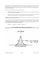
Figure 2.5 Definition of Spatial Resolution (Resolvable Element) . . . . . . . . . . . . . . . . . . . . . . . . . . . . . . . page 41
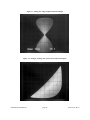
Figure 3.1 Analog X-Y Image, Full Active Area . . . . . . . . . . . . . . . . . . . . . . . . . . . . . . . . . . . . . . . . . . . . page 43
Figure 3.2 Analog X-Y Image, Emission Point Defect . . . . . . . . . . . . . . . . . . . . . . . . . . . . . . . . . . . . . . . page 43
Figure 3.3 Analog X-Y Image, Input Leads Interchanged . . . . . . . . . . . . . . . . . . . . . . . . . . . . . . . . . . . . . page 44
Figure 3.4 Analog X-Y Image, One Corner Not Connected Properly . . . . . . . . . . . . . . . . . . . . . . . . . . . . page 44
Figure 3.5 Analog X-Y Image, Two Opposite Corners Not Connected Properly . . . . . . . . . . . . . . . . . . . . page 45
Figure 3.6 Digital Image, Incorrect ADC Span and Zero Adjustments . . . . . . . . . . . . . . . . . . . . . . . . . . . page 45
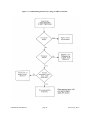
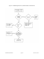
Figure 3.7 Troubleshooting Decision Tree, Image on CRT Not Circular . . . . . . . . . . . . . . . . . . . . . . . . . . page 46
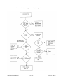
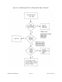
Figure 3.8 Troubleshooting Decision Tree, No Output From Detector . . . . . . . . . . . . . . . . . . . . . . . . . . . . page 47
Figure 3.9 Troubleshooting Decision Tree, Insufficient Number of Events Detected . . . . . . . . . . . . . . . . page 48
Figure 3.10 Troubleshooting Decision Tree, Background Too High or "Hot Spots" . . . . . . . . . . . . . . . . . . page 49
3300/2400 System Manual
page 5
18 Nov 2013, Rev I
This page is intentionally blank
3300/2400 System Manual
page 6
18 Nov 2013, Rev I
LIMITED WARRANTY
Quantar Technology products are warranted against defects in material and workmanship for a period of one year from
the date of shipment. During the warranty period, Quantar Technology will, at our option, repair, replace or refund
the purchase price of products which prove to be defective. For warranty service or repair, this product must be returned
to Quantar Technology.
For products returned to Quantar Technology for warranty service, Buyer shall prepay shipping charges to Quantar
Technology and Quantar Technology shall pay shipping charge to return the product to Buyer. However, Buyer shall
pay all shipping charges, duties, and taxes for products returned to Quantar Technology from another country.
LIMITATION OF WARRANTY
The foregoing warranty shall not apply to defects resulting from improper or inadequate maintenance by Buyer, Buyersupplied software or interfacing, unauthorized modification or misuse, operation outside of the environmental
specifications for the product, or improper site preparation or maintenance.
Special Notes regarding MCP's and products containing MCP's (microchannel-plate electron multipliers):
Warranty does not cover damage to MCP's caused by warpage or cracking due to improper storage, shock, vibration,
contamination or improper handling. Users are cautioned that MCP's are sensitive to water vapor absorption and may
warp and crack if stored outside of clean vacuum systems for extended periods.
For sealed-tube detectors, warranty does not cover damage resulting from exposure to excessive input radiation levels,
thermal shock, exposure to temperatures below -30° C or above +45°C, excessively rapid rates of change of
temperature, mechanical shock or excessive high voltage applied to tube.
NO OTHER WARRANTY IS EXPRESSED OR IMPLIED. WE SPECIFICALLY DISCLAIM IMPLIED
WARRANTIES OF MERCHANTABILITY AND FITNESS FOR A PARTICULAR PURPOSE.
EXCLUSIVE REMEDIES
THE REMEDIES PROVIDED HEREIN ARE BUYER'S SOLE AND EXCLUSIVE REMEDIES. NEITHER
QUANTAR TECHNOLOGY NOR ANY OF ITS EMPLOYEES SHALL BE LIABLE FOR ANY DIRECT,
INDIRECT, SPECIAL, INCIDENTAL, OR CONSEQUENTIAL DAMAGES ARISING OUT OF USE OF ITS
PRODUCTS, WHETHER BASED ON CONTRACT, TORT OR ANY OTHER LEGAL THEORY, EVEN IF
QUANTAR TECHNOLOGY HAS BEEN ADVISED IN ADVANCE OF THE POSSIBILITY OF SUCH DAMAGES.
SUCH EXCLUDED LOSSES SHALL INCLUDE, BUT ARE NOT LIMITED TO: COSTS OF REMOVAL AND
INSTALLATION, LOSSES SUSTAINED AS THE RESULT OF INJURY TO ANY PERSON, OR DAMAGE TO
PROPERTY.
3300/2400 System Manual
page 7
18 Nov 2013, Rev I
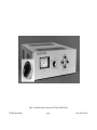
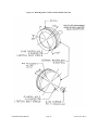
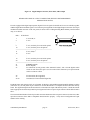
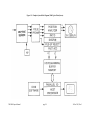
Figure 1.0 Model 2401 Position Analyzer and 3300 Series MCP/RAE Sensor
3300/2400 System Manual
page 8
18 Nov June 2013, Rev I
GENERAL INFORMATION
1.0
SCOPE OF THIS MANUAL
This Quantar Technology 3300/2400 SYSTEM INSTALLATION AND OPERATION MANUAL provides information
regarding the system-level set-up, installation and operation of the Series 3300 Open-Face MCP/RAE Sensors when
operated together with the Model 2401 Position Analyzer. It is intended to be used with the separate manuals for the
3300 Series Sensors and the Model 2401 Position Analyzer, which provide more detail on these individual models,
especially regarding corrective repair and maintenance. All circuit schematics and component locators for the Model
2401 are contained in its specific manual.
Manual Update Inserts may be provided with this manual that update information regarding manual errors or design
changes.
1.0.1
GENERAL DESCRIPTION
A 3300 Series MCP/RAE Sensor (detector head) operated with the Model 2401 Position Analyzer and auxiliary HV
bias supplies and data collection systems forms a single-event-counting, high-sensitivity, position-sensitive imaging
detector system for scientific applications. The detector system is sensitive to charged-particles, neutral-particles, and
energetic photons (EUV, soft X-ray), and operates in vacuum environments. This single-event-counting sensitivity
combined with extremely low detector-generated-background results in exceptionally good signal-to-detectorbackground performance. Applications range from 1-D use in multichannel spectroscopy, such as XPS, to 2-D imaging
spatially-resolved spectroscopy, to full 2-D X-Y imaging.
The system is available in two versions. The standard spatial-resolution version (FWHM resolution of 1/100 of active
diameter) uses 2 MCP's in the sensor with a mean electron gain of approximately 5 x 10 6 and the Option EM preamp.
The high spatial-resolution version (FWHM resolution of 1/400 of active diameter) uses 3 or 5 MCP's in the sensor
with a mean electron gain of approximately 5 x 10 7 and uses the Option EP Preamp. Preamp gain is different in the
two options to compensate for the output levels of the two sensor types.
3300/2400 System Manual
page 9
18 Nov 2013, Rev I
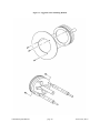
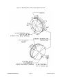
Figure 1.1 Suggested Sensor Mounting Methods
3300/2400 System Manual
page 10
18 Nov 2013, Rev I
SECTION 1. SYSTEM INSTALLATION
1.1
SENSOR ASSEMBLY MOUNTING
The detector assembly can be physically mounted either from the rear ceramic baseplate or from the front mounting
ring.
To mount from the rear baseplate, use the clearance holes (0.140 inch, 3.6 mm diameter) provided in the baseplate for
mounting the sensor on machined support posts or tabs from the rear (e.g. from a vacuum flange). See Figure 1.1, 1.2
(25mm) and 1.3 (40mm). Since the ceramic baseplate is electrically isolated from all electrodes, supporting hardware
can be maintained at any desired potential with respect to the detector. If using machined mounting posts, use either
threaded ends with low-profile nuts (to avoid interference with the close-proximity RAE substrate) or machined "C"
ring grooves and matching "C" rings and spring washers to hold the detector in place on the ends of the posts. There
is limited clearance space between the location of the mounting holes for such posts and the edge of the relatively
fragile RAE substrate, so care must be exercised to avoid damage due to tool slippage, etc.
To mount from the front surface, 0-80 size screws can be used to mount to the front ring which has several 0-80
threaded holes. Be certain that the screws are not excessively long, such that they could electrically short the front and
rear rings, which will result in arcing and improper operation.
If the sensor is to be mounted from the front ring, be certain the surface to which it is to be mounted can be operated
at the same electrical potential as the front ring, which is at the same potential as the front MCP surface. Whether the
front surface of the sensor is operated at ground potential or a high negative potential depends on the biasing
arrangement chosen by the user based on the application details. Generally, it is desirable to avoid potentials on the
first MCP surface which will attract stray charged particles in the vacuum chamber.
If the sensor is equipped with option 001/SE, Additional Electrically-Isolated Front Ring, the sensor can be supported
from this ring in the manner described above, and the Option 001/SE ring can then be maintained at any desired
potential within 2 kV (the approximate breakdown voltage) of the input MCP electrode voltage.
The sensor can be mounted on a standard Conflat-type, copper or O-ring gasket, vacuum flange (rotatable type is
sometimes preferred to enable alignment of detector axes if necessary). Generally the smallest size flange that can be
used for mounting is a 4-5/8 inch size Conflat-type the smallest for the 25mm and 40 mm size sensors (a 4-1/2 inch
Conflat flange can be used but the ID of the copper sealing gasket generally must be modified). An 8-inch diameter
Conflat-type flange is required for the Model 3392A 75 mm MCP/RAE Sensor and larger sensors.
1.2
MOUNTING OF ELECTRONICS MODULES
The main chassis of the Model 2401 Position Analyzer may be used either as a stand-alone unit or mounted in a
standard 19-inch wide electronics rack using the rack mounting brackets supplied. Handles for convenience in lifting
are mounted on the rack adapter brackets. When mounting in an electronics rack with other equipment, proper
grounding procedures should be followed to avoid generation of noise and ground loop currents.
3300/2400 System Manual
page 11
18 Nov 2013, Rev I
Figure 1.2 Mounting Hole Locations, 25 mm, Models 3390, 3391
3300/2400 System Manual
page 12
18 Nov 2013, Rev I
Figure 1.3 Mounting Hole Locations, 40 mm, Models 3394, 3395
3300/2400 System Manual
page 13
18 Nov 2013, Rev I
The 24012 Preamplifier Module should be mounted as close to the MCP/RAE Sensor as possible to minimize lead
capacitance at the input of the charge-sensitive circuits. It is recommended that the preamp be mounted to a common
electrical ground point on or close to the vacuum flange for the signal and HV vacuum feedthroughs. It may be
mounted on a user-supplied metal bracket using two or more of the 4-40 size machine screws that can be seen on the
bottom surface of the preamp module case. It may be necessary to use slightly longer screws, depending on the
thickness of the mounting bracket. The bracket should then be mounted securely to the vacuum chamber. Even a few
ohms resistance in this grounding path can result in ground loop noise voltages. It may be necessary to experiment
with the optimum grounding procedure for a particular setup to minimize noise pickup (see SUM pulse diagnostic
measurements, section CHECKING NOISE LEVEL).
1.3
BIASING AND ELECTRICAL CONNECTIONS - CONNECTING SENSOR TO PREAMP
1.3.1 SYSTEM INTERCONNECTION DIAGRAMS.
See Figures 1.4 and 1.5, Electrical Connections, for identification of contacts on rear of 3300 Series MCP/RAE
Sensors.
Figures 1.6, 1.7 and 1.8, System Interconnection and Biasing, provide schematic information for hookup of signal
leads, HV leads and the HV Bias Voltage Divider. The following sections should be read with reference to these
figures.
SAFETY WARNING
The electrical potentials applied to this MCP sensor for proper operation are potentially
harmful. Personnel should use extreme care in handling HV leads, making connections and
performing tests.
1.3.2 SIGNAL LEADS
Signal connections from the 4 contacts (corners) of the RAE should be shielded if over about 4 inches (10 cm) long
due to the extreme sensitivity of the charge-sensitive amplifiers to extraneous electrical signals which can be generated
either inside or outside the vacuum system. Use the lowest-capacitance coax cable available that is compatible with
your UHV environment requirements to minimize additive noise at the input of the charge-sensitive amplifiers (due
to cable capacitance) which will degrade the spatial resolution (increase position jitter) of the system. A maximum
of about 60 pF (picofarads) capacitance to ground is permissible in each signal lead to the preamplifier without
adversely affecting spatial resolution. Low-capacitance coax cable with Teflon insulation (e.g. RG187/188 type, 30 pF
per foot) can be used if compatible with the specific vacuum environment and temperature requirements of the
application (probable maximum vacuum of 10-9 and maximum temperature of 150 degrees C). Shielded bakeable
ceramic-bead-insulated coax is available from Ceramaseal Corporation (see below**).
**For UHV-compatible, bakeable shielded cable assemblies for use in bringing RAE signal
leads from sensor to vacuum feedthrough it is suggested to contact: Ceramaseal Corporation,
New Lebanon, New York, 121256; Tel: 518/794-7800 or 800-752-7325; FAX 517/794-8080;
www.ceramseal.com. Or, Insulator Seal Div of MDC, Sarasota FL 34243 Tel: 941-751-2880
FAX: 941-751-3841 www.isi-seal.com. Request information on "In-Vacuum Cable
Assemblies." Desired cable lengths and connector types must be specified before ordering.
3300/2400 System Manual
page 14
18 Nov 2013, Rev I
Generally, attempt to keep the total length of signal leads less than 24 inches (0.6 meter) from sensor to preamplifier
(i.e. both inside and outside the vacuum). Longer leads may be used, but some increased position jitter or noise pickup
may be experienced (depending on noise sources present). may
If signal leads are shorter than 4 inches, shielding is typically not required except in extremely noisy electrical
environments.
1.3.3 ORIENTATION OF SIGNAL LEADS: A, B, C, D.
In order to produce a proper image, the signals from the RAE must be connected in the proper orientation. The
following procedure is recommended for connection of the signals from the sensor. First, designate any of the four
corners of the sensor as "A." Connect this output to preamp input A. Moving counterclockwise around the sensor,
as viewed from the rear, designate the next corner as B and, likewise, connect to preamp input B. Continue this
sequence for C and D. The rotational orientation is arbitrary, except for mirror imaging the signals. However, in any
case, the A, B, C and D leads must follow each other in consecutive order. If any two adjacent leads are interchanged,
a "twisted" image will result (see Maintenance section and Figure 3-3).
1.3.4 SIGNAL LEAD DECOUPLING
The preamp inputs are direct-coupled and cannot tolerate any DC bias. Each signal output lead is capacitively
decoupled by 1000 pF ceramic block capacitors mounted on the rear of the ceramic baseplate. These capacitors are
rated at a maximum of 5000 VDC. The purpose of these capacitors is to enable biasing of the anode at a high DC
potential relative to ground and yet to avoid applying this high voltage to the preamplifier signal inputs, which will
be damaged by any substantial DC voltage and also to reduce the required voltage rating of the coaxial signal leads.
1.3.5 HV LEADS
The number of HV leads required depends on whether the HV Bias Voltage Divider is located inside the vacuum
system or outside. For all leads inside the vacuum system, it is recommended that some type insulated wire be used
to avoid corona discharge and shorting which would adversely affect detector operation. Teflon-insulated wire is
suitable for use in some vacuum systems while other insulation methods should be used for other vacuum system
environments, depending on the application and level of operating pressure. All HV leads outside the vacuum chamber
should be appropriately insulated and shielded to avoid noise pickup.
1.3.6 VACUUM FEEDTHROUGHS
Separate BNC-type and SHV-type feedthrough connectors have been found to be most practical. Multi-pin feedthrough
connectors can be used provided the voltage rating is sufficient and the interelectrode capacitance is minimized (1-2
pF). Signals are not of the frequency range to require use of feedthroughs with a defined 50 impedance.
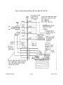
4 BNC-type feedthrough connectors are required for signal output leads and, depending on the location ofthe HV Bias
Voltage Divider network, a suitable number of SHV-type (5KV rating) HV feedthroughs for HV bias voltage leads.
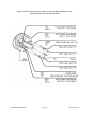
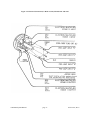
Using an external HV divider, for 2 MCP versions and 3 MCP Option 010 version, the following are required: RAE
bias (Vrae), MCPout (Vout), MCPcenter (Vctr), MCP in (Vin). See Figure 1.6 & 1.7.
Using an external HV divider, for 5 MCP versions, the following are required: RAE bias, Stage 2 Out (Zout), Stage
2 In (Zin), Stage 1 out (Vout), Stage 1 in (Vin). See Figure 1.8.
An additional HV feedthrough is required if the option SE Extra Front Ring is to be biased. In addition, it is often
desirable to use a separate pin feedthrough for the common signal coax shield ground lead as shown in the diagrams.
3300/2400 System Manual
page 15
18 Nov 2013, Rev I
Figure 1.4 Electrical Connections for 2 MCP versions and 3 MCP Option 010 versions,
Models 3390 and 3394; 3391-010 and 3395-010
3300/2400 System Manual
page 16
18 Nov 2013, Rev I
Figure 1.5 Electrical Connections, 5 MCP versions, Models 3391 and 3395
3300/2400 System Manual
page 17
18 Nov 2013, Rev I
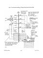
1.3.7 GROUNDING AND BYPASSING
The signal leads are extremely susceptible to pickup of electrical noise, radio frequency interference (RFI) and
transients from the electrical environment. Hence, they should be adequately shielded.
Give particular attention to minimizing signal ground loops, which will interfere with proper operation of the sensor,
by properly terminating grounded shields of coax cables and avoiding the use of multiple grounding points which may
be at slightly different actual electrical potentials. For example, it is typically desirable to ground only one end of the
signal coax cable shields, not both ends. If grounded at the sensor (detector head) end, bring a single ground lead out
from the common shield connection out through an isolated vacuum feedthrough and ground at a common point with
the preamplifier (See block diagram, either Figure 1.6, 1.7 or 1.8). The shields should be grounded at one point as
physically near the MCP/RAE sensor as possible.
Small ceramic bypass capacitors are recommended as shown in Figures 1.6, 1.7 and 1.8 to provide extra current to the
last MCP's during event multiplication and to bypass high-frequency noise to ground. Select capacitors with
appropriate voltage ratings based the HV bias levels used.
A convenient way to observe and quantify the quality of the grounding is to connect an oscilloscope to the SUM output
with the scope external trigger input connected to the RATE output of the Model 2401. Adjust the scope TRIGGER
LEVEL manually. This will display the incoming pulses in sync and allow them to be differentiated from noise. By
setting the scope sensitivity to about 5 mV per division, the background noise can be also observed as the SUM pulse
completes its positive-leading bipolar cycle and returns to the baseline. Background noise above 15 mv peak-to-peak
can cause degradation in the system spatial resolution. This is discussed further in Section 2, System Operation, and
Figure 2.1, SUM PULSE NOISE.
To isolate sources of local noises and interference, monitor the noise on the SUM signal as described above and turn
ON and OFF possible sources of noise (ion gauges, pumps, stepper motors, computer switching-type power supplies,
etc.) until the source of noise is identified. It can then often be corrected by improved grounding or shielding.
NOISE PICKUP AND GROUNDING
The outer shield of a coaxial cable serves to interconnect the chassis of each instrument
module with that of the next. When all components are mounted in an instrument rack, this
electrical connection is often redundant. When components are physically separate, however,
the shield will tend to establish a common ground potential for all components. If all chassis
are not grounded internally to the same point, some dc current may need to flow in the shield
to maintain the common ground potential. In many routine applications, this ground current
is small enough to be of no practical consequence. However, in low-signal-level systems like
the Series 3300/2400, this current can be large compared to signal currents from the RAE. If
components are physically separated and internally grounded under widely different
conditions, the shield current can be large and its fluctuations may induce significant noise in
the cable and preamp. Under these conditions, such "ground loops" must be eliminated by
ensuring that all components are internally grounded to a single common point for the entire
system.
3300/2400 System Manual
page 18
18 Nov 2013, Rev I
1.3.8 HIGH VOLTAGE BIAS
CAUTION
Carefully avoid placing any HV bias voltage on the preamplifier inputs. To do so may
permanently damage the input FET, protection diodes and other circuitry.
Adequate MCP gain is necessary to enable the sensor to detect incoming events with desired spatial resolution. In turn,
MCP gain is critically dependent on the magnitude of the HV bias applied to each MCP between its input surface
electrode and output electrode.
In addition, a sufficient and uniform electric field must be maintained between the last MCP surface and the RAE for
proper imaging.
The HV bias provides both of these voltages through use of a user-supplied resistive voltage divider network and HV
power supply (with low ripple and noise).
1.3.9 HIGH VOLTAGE DIVIDER NETWORK
The bias voltages for the sensor are typically provided by external resistive voltage dividers and HV power supplies.
It is also possible to construct resistive voltage dividers inside the vacuum system using vacuum-compatible (e.g. glass)
resistors that have been suitably cleaned of oils and silicone greases. While less flexible and accessible due to location,
this method minimizes the number of HV vacuum feedthroughs that are required. This method is particularly simple
for 2 MCP sensors since only three resistors are essential (ignoring the series current-limiting resistors that are
recommended but not required).
Proper operating HV levels differ slightly for each MCP/RAE sensor, based on differences in MCP gain versus voltage
characteristics. Consult the Final Performance Test Report supplied with each Quantar Technology 3300 Series
MCP/RAE sensor for values found to be suitable in final test. Also see Section 2.2, HV Optimization, in this manual.
Construct a HV resistive divider network in a shielded, grounded, protective metal enclosure that provides sufficient
safety for operating personnel. The total resistance of the voltage divider string should be such that a minimum of 400500 microamps current flows in the divider resistor string (at least about 10X the quiescent, no-signal, bias current)
while the desired voltages are developed for each MCP and RAE electrode. This ensures that the HV bias voltage will
not fluctuate significantly due to varying signal currents in the MCP's, which can result in fluctuating and decreased
gain. Often, it is preferable to wire the HV resistors only to each other and connectors, not using a PC board for
mounting but relying on air dielectric for protection against breakdown. If a PC board is used, be certain the board
and the lead spacing is of a suitable material to withstand the voltages involved.
Calculate and select each resistor of the divider chain to produce the desired voltage for a specific electrode contact
in the MCP/RAE Sensor. It is recommended to use HV-type resistors to avoid breakdown or use multiple resistors in
series to keep the voltage across any single resistor within its rated limits. During setup, variable resistors (with HVinsulated shafts and mountings) may be temporarily used to optimize voltages but should be replaced by fixed resistors
in the final voltage divider. To meet the desired voltage and total current requirement with commercially available
resistor values may require several iterative calculations. Calculate the power dissipation (P=I2 x R or P=I x E) of each
resistor and select resistors of appropriate power rating.
The polarity of the HV is determined by the configuration considerations discussed in Section 1.3.10, HV Bias
Configurations of this manual.
3300/2400 System Manual
page 19
18 Nov 2013, Rev I
Figure 1.6 System Interconnection and Biasing, 2 MCP Sensors, Models 3390, 3392 and 3394
3300/2400 System Manual
page 20
18 Nov 2013, Rev I
Figure 1.7 System Interconnection and Biasing, 3 MCP Option 010 Sensors, Models 3391-010 and 3395-010
3300/2400 System Manual
page 21
18 Nov 2013, Rev I
Figure 1.8 System Interconnection and Biasing, 5 MCP Sensors, Models 3391 and 3395
3300/2400 System Manual
page 22
18 Nov 2013, Rev I
Each MCP requires approximately 700-1000 VDC. The exact voltage to produce the desired level of electron gain
(and, therefore, spatial resolution) without introducing excessive background varies from unit to unit. The MCP
voltage used in production tests will be indicated on the test data supplied with each sensor. Some experimentation
with this voltage by the user can often result in an optimum voltage for a specific application environment. In no case
should the bias voltage need to exceed 1000 VDC per MCP. The voltage bias between the output of the last MCP and
the RAE is not critical in most environments (providing there are no strong transverse magnetic fields) but should be
at least 200 volts and no more than 500 volts.
The RAE is normally biased through the 1 megohm s (vacuum-compatible) resistor supplied with the sensor and
mounted on the rear surface of the ceramic baseplate. This resistor presents a much higher impedance than the
approximately 50 ohm input impedance of the preamplifiers and thus results in essentially no signal loss, yet provides
a fixed bias path to the RAE to maintain a uniform electric field between the last MCP surface and the RAE which is
necessary for proper spatial imaging.
It is recommended that series current-limiting resistors be installed in each HV lead from the voltage divider to the
MCP's. These will limit the current that can flow in the event of arcing or field emission upon application of high
voltage bias. This, in turn, will limit damage to the MCP's. Any voltage drop across the series resistance must be
accounted for in arriving at the correct bias voltage to the MCP itself. Test data sheets supplied with the unit indicate
the bias (strip) current of each MCP and are typically in the range of 25 to 60 microamps depending on type and size,
with special MCP types exhibiting even higher bias currents. The HV bias levels shown on the test data supplied do
NOT include any adjustment for a voltage drop across a series limiting resistor.
1.3.10 HV BIAS CONFIGURATIONS
The sensor may be operated in either of two configurations. In either configuration, electrical potentials must always
become increasingly positive from the front surface of the detector to the RAE at the rear so secondary electrons are
accelerated toward the RAE.
1.3.10.1. FRONT MCP AT GROUND POTENTIAL:
In this case, the front surface of the sensor is operated at ground potential. Each succeeding stage must be operated
at a progressively more positive potential so that electrons generated in the MCP's will be accelerated. The RAE will
be at the highest (and positive) potential in this configuration. Assuming this configuration is satisfactory from the
standpoint of the remainder of the application set-up (e.g. energy analyzer potentials), this is often the easiest way to
operate the sensor.
1.3.10.2. FRONT MCP SURFACE AT NON-GROUND POTENTIAL:
In this case, the front MCP will most often be operated at a high negative potential. Each succeeding stage will be
operated at a lower negative potential. The RAE will then typically be at ground potential or close to ground.
Operation in this mode may result in stray charge particles in the vacuum chamber (originating from various processes)
being attracted to the MCP and being detected as increased background.
In addition, the sensor may be operated with both front MCP and RAE at non-ground potentials, providing the
potential differences are correct between MCP stages (always accelerating electrons toward the RAE) and the voltage
rating of the decoupling capacitors is not exceeded.
3300/2400 System Manual
page 23
18 Nov 2013, Rev I
1.4
CONNECTING PREAMP TO POSITION ANALYZER
The preamp has 6 connections which go to the position analyzer, including 5 signal outputs and a power connector.
Outputs A through D correspond to inputs A through D and carry amplified and shaped signals from the four corners
of the detector. Output E is a fast version (higher bandwidth) sum of the input signals to the preamp which is used
by the position analyzer for look-ahead and pulse-pile-up rejection timing. Connect A to A, B to B and so on. Signals
A through D come from identical preamps and may be interchanged to correct for improper arrangement of the preamp
inputs from the MCP/RAE sensor or for purposes of troubleshooting. An 8-foot (2.4 m) cable is supplied for
interconnecting these signals to the position analyzer. A longer cable up to 17 feet (5.1 m) in length may be substituted
without significant signal degradation.
1.5
CONNECTING POSITION ANALYZER TO EXTERNAL DEVICES
The following sections discuss the function and characteristics of the rear panel outputs and switches on the Model
2401B Position Analyzer. For additional detail on the waveforms of these signals, consult the Model 2401B Operating
and Service Manual.
1.5.1 ANALOG X AND Y POSITION SIGNALS
These signals are the primary analog event position outputs from the system. They are intended to be connected to the
X and Y axes of an oscilloscope, producing a real-time monitor image of the incoming flux. They can also be
connected to a user-supplied analog-to-digital converter or digitizing multi-channel-analyzer (MCA).
The amplitude voltage (of the valid flat top portion) of these pulsed position signals ranges from approximately 0.5
to 4.5 volts, and is linearly proportional to the coordinate position of the most recently processed event, starting from
one edge of the active area diameter of sensor and ending at the other edge (along diameter on each axis). These
signals should be read by external devices only during periods when the STROBE signal (see below) is valid. This
assures these signals are properly settled. These analog position signals are present for the following times (which are
slightly less than the total dead-time of the Model 2401 version being used): 3 sec (analog only and 8-bit digitized
output option), 5 sec (9-bit option) and 8 sec (10-bit option).
Note regarding use with external MCA's (multi-channel-analyzers): The standard quiescent level (between events)
of these X and Y position signals is 2.5 volts. As a result, the leading edge of the X, Y (or both) position pulses of an
event located to the left and lower of the image center will have a negative-going leading edge. This confuses some
MCA-type pulse-height analyzers (especially those without an externally-triggered Sampled Voltage Analysis Mode)
which require a positive-going leading edge on all input pulses to enable the proper sampling of the peak voltage. A
special interface option is available for the Model 2401B, called the MCA Interface Option, for these situations and
returns the inter-event voltage to 0 volts so the leading edge of the position pulse is always positive-going. Up to Model
2401A serial number 7440, this option was supplied on a plug-in board. Starting with that serial number, the
components for this option are installed on a special section of the main board.
3300/2400 System Manual
page 24
18 Nov 2013, Rev I
1.5.2 Z AXIS
The Analog X and Y position outputs return to their quiescent level between event computations and would normally
be displayed on the oscilloscope screen. However, in order to eliminate the fuzzy bright spot and traces which would
appear on the display due to this dwell time, the Z-axis signal provides a properly timed 15 volt signal which blanks
the CRT screen except at times when the outputs represent a valid event computation, in which case a bright dot
appears at the appropriate point on the screen.
CAUTION
Do NOT connect or disconnect the Z-axis cable while either the oscilloscope or the 2401 is
powered on. Due to the presence of appreciable voltages on the Z-axis of some oscilloscopes,
the Z axis output circuit (U120) of the Model 2401 can be damaged if this is done. Always
turn oscilloscope power and Model 2401 power OFF before connecting or disconnecting the Zaxis lead.
The timing of the Z axis signal is the same as the Strobe signal. The Z-axis signal changes from +15 V to 0 volts for
approximately the following periods: 4 sec (analog only and 8-bit digitized output options), 6 sec (9-bit digitized
output) and 10 sec (10-bit digitized output). This Z-axis output is compatible with the Z-axis Intensity Blanking
function on the most popular laboratory oscilloscopes (Tektronix, HP, etc).
1.5.3 STROBE
The analog strobe signal is a TTL-level signal which normally goes to 5 volts for the time period during which the
analog X, Y position signal outputs are stable and readable. It can be used to trigger external A-to-D conversion or
other logic. Connect to digital frequency counter to monitor STROBE count rate to measure total number of fullyprocessed events per second. There is a single STROBE pulse generated for every valid, fully-processed event. Polarity
is selected by a board-level STROBE jumper (see Control Logic Component Locator, Jumper is located next to IC
U122; use 2 pins nearest edge of board for 0V to +5V leading edge; use 2 pins farthest from edge of board for +5V
to 0V leading edge). Duration of the STROBE pulse is dependent on the digitized output options, similar in operation
to the Z-axis. Note: RATE is monitored by the front-panel meter; STROBE rate is not monitored).
1.5.4 SUM
The SUM signal is the arithmetic sum of the output signals from the four shaping preamps (channels A through D).
It is used as a diagnostic signal for observing the total pulse amplitude levels, indicating the size of the charge pulse
deposited on the RAE from the MCP's and a direct indication of MCP electron gain, and enabling the adjustment of
the HV bias to the appropriate level to generate the proper MCP gain. The SUM signal can also be used for observation
of random noise and transient pickups by the system which can be detrimental to performance.
1.5.5 BUSY
The busy signal is a, TTL-level signal which goes from 0 volts to a logical high when triggered by the RATE lowerlevel threshold comparator (about 150 mV) and indicates the BUSY one-shot circuit is in a timing sequence. The
"busy" monostable produces a signal slightly longer than the pulse duration of the four shaper amplifiers (for a single
detected event it has a 2.8 msec duration) and is retriggerable. Any additional pulse arriving within the busy period
of a previous pulse will retrigger the "busy" timeout and will result in a longer pulse duration. It is useful in observing
the preamp-associated dead-time.
3300/2400 System Manual
page 25
18 Nov 2013, Rev I
1.5.6 RATE
The RATE signal represents the total incoming rate of pulses which exceed the RATE threshold (150 mV on SUM
signal). A separate RATE pulse is generated for each event that is time-separated by a least 400 nsec from a prior
event. Pulse duration is 0.6 sec and the leading edge moves from the TTL-low level to the TTL-high level. Pulses
are further tested for level and timing before actual processing and some events included in RATE may be vetoed later
from further processing. The RATE output is useful for determining actual (true) input rate as compared to output rate
available at the strobe (imaged) output to determine the fraction of input pulses being processed. See notes elsewhere
in this manual regarding RATE channel deadtime.
The RATE includes events that may later be vetoed from further processing (and not included in the Strobe) due to
edge-gating settings, failure to exceed the Strobe lower threshold (300 mV on SUM pulse), pulse-pile-up rejection (see
dead-time discussion below) or pull-down of the external Veto Gate Input (2401B only). The RATE will always equal
or exceed STROBE. The ratio of STROBE to RATE enables calculation of fractional dead-time loss (1-ratio). The
RATE output can be connected to a digital frequency counter for monitoring (adjust counter’s threshold carefully to
avoid double counting). This signal is equivalently monitored by the front panel meter when the Meter Switch is in
the Count Rate position.
1.5.7 VETO GATE INPUT (Model 2401B version only, beginning October 1990).
This input provides for external, time-based digital control of processing. Grounding of this rear-panel input interrupts
both analog and digital output until it is released from ground. This capability is useful in applications where it is
desirable to exclude processing of events to an external data system or memory during specified periods which are
synchronized to external experimental conditions (e.g. low-rep-rate pulsed laser excitation of a sample). The precision
(time-jitter) for the cut-on and cut-off of processing is approximately 300 nsec. This input is pulled-up to the "normal
status" by internal resistors when the input has no connection and signal input should never excess of 5 volts.
If an event is NOT to be vetoed, the VETO GATE signal must be in high state no later than 20-30 nsec after the event
occurs (when the FAST RATE signal appears on U115b) and must continue to be in the high state up to approximately
800 nsec (peak time, PK-TH). If it is allowed to go low at any time in this interval, then the event will be vetoed from
further processing. If an event IS to be vetoed, the VETO GATE must be pulled LOW at least sometime before 500
nsec after the event occurs, and held low through about 800 nsec.
1.5.8 DIGITAL X AND Y POSITION SIGNALS
The digitized position output signals are TTL-level, positive-true signals and are provided on data lines (8, 9 or 10
lines), each with a separate ground connection, plus a Digital Strobe ("read-me" signal). Refer to Figure 1.9 for details
regarding the connector designations.
1.5.8.1 DIGITAL STROBE
1.5 msec duration, negative true logic, TTL-level pulse that accompanies digitized position signals to latch data or
trigger to be read by external data device (memory, computer, etc). Digital Strobe starts immediately at end of ADC
conversion (later than the analog strobe), which depends on digital option. Not available on analog only versions.
Goes from TTL-high level to TTL-low level on leading edge.
3300/2400 System Manual
page 26
18 Nov 2013, Rev I
Figure 1.9 Digital Output Connector, Rear Panel, ADC Output
REAR PANEL DIGITAL OUTPUT CONNECTOR (WITHOUT HISTOGRAMMING
MEMORY INSTALLED)
For units equipped with digital output options, digital TTL-level signals for both X and Y axes are available, together
with the Digital Strobe and Rate signals. The connector pin assignments for the Digital Output Connector (the 50-pin
3M brand D ribbon connector on the rear panel) for units without a Histogramming Buffer Memory board installed
only, are as follows:
PIN #
FUNCTION
1
Y axis LSB, 20
2
Y axis
.
.
.
.
9
Y axis, used only for 9 and 10 bit options
10
Y axis, used only for 10 bit options
------------------------------------------------------------------------11
X axis, LSB, 20
12
X axis
.
.
.
.
19
X axis, used only for 9 and 10 bit options
20
X axis, used only for 10 bit options
------------------------------------------------------------------------21
STROBE (Digital)
22
RATE (Digital)
23
No connection (do not ground). After 2401B S/N 95467, with 1-D/2-D digitial switch
circuit on main board, this pin is used for control of this function by rear panel manual
switch or software control.
24
25
26-50
No connection (do not ground)
No connection (do not ground)
Grounded (for each individual digital bit)
For Model 2401 units equipped with one of Quantar Technology's optional Histogramming Buffer Memory modules
(2412/2415 etc), the rear panel 50-pin connector is used for the interface to a computer IO board from the memory
board. The digitized output from the main board is connected to the input of the memory board. Consult the manual
for the appropriate model memory board for pin assignments for the rear-panel 50 pin connector which differ from the
above.
The current 3M Part Number for the 50-pin cable connector that mates to this rear panel connector is 3564-1001; other
equivalent connectors from AMP or Amphenol should interface properly. Verify desired configuration and part
number before ordering.
3300/2400 System Manual
page 27
18 Nov 2013, Rev I
1.6 REAR-PANEL SWITCHES
1.6.1 Y-AXIS DIGITAL OUTPUT MODE SWITCH - PULSE HEIGHT MEASUREMENT
This switch, located on the rear panel, selects the input signal to be digitized by the optional Y-Axis A-to-D converter.
In the normal position, the converter digitizes the Y-Position signal. In the PHA position, the converter digitizes the
peak values of the SUM pulses, creating a digitized pulse height distribution (number of events on vertical axis and
relative SUM pulse amplitude on the horizontal axis) which is useful for more precise evaluation of MCP gain.
Observation of this digitized Pulse Height Distribution requires a digital data collection system. See Figure 2.1 and
2.2, Typical Pulse Height Distribution.
1.6.2 1-D/2-D DIGITAL MEMORY MAPPING CABLE SWITCH
This switch controls the mode of the optional Switchable Digital Memory Mapping Cable linking the ADC output with
the address input port of the Model 2412A or 2415A Histogramming Buffer Memory. It enables switching between
1-dimensional (Y-axis only) and 2-dimensional (Y and X axes) operation without physically exchanging the Digital
Memory Mapping Cable (flat multiconductor ribbon cable) which is normally required when changing between 1-D
and 2-D data accumulation.
In 2401B units with SN 95467 and above (approx Dec 1995), this 1-D/2-D switching function is implemented on the
main board. It is designed primarily to be controlled by Quantar Model 2251A MCA/MCA2D Software. It can be
controlled by an optional rear-panel switch as well which is normally not installed. If the switch is installed, it must
be left in the 2-D position in order for the software to be able to control the switching function. Consult the factory
for details of installing this manual switch if desired.
3300/2400 System Manual
page 28
18 Nov 2013, Rev I
Figure 1.10 Complete System Block Diagram (With Typical Data System)
3300/2400 System Manual
page 29
18 Nov 2013, Rev I
SECTION 2. SYSTEM OPERATION
2.1 INITIAL TURN-ON AND CHECKOUT
2.1.1 SYSTEM SET-UP
Connect the various system components as described in the SYSTEM INSTALLATION section of this manual.
WARNING
The Model 2401B is equipped with a switchable AC power input module. To avoid serious damage, this
module must be set to the appropriate LINE VOLTAGE before inserting the power cord. The operating
voltage is set by the orientation of the small removable printed circuit insert card in the power module.
To access this card, slide the plastic cover to the left and remove the PC card with thin pliers. Reinsert
with the appropriate marking for 100/120/220/240 VAC in the position that matches the line voltage
being used.
2.1.2 VACUUM PRESSURE
When the sensor is first installed, substantial outgassing of the adsorbed gases on the large surface area of the MCP's
and other components will normally occur. It is recommended that the sensor be resident in the vacuum system at a
pressure lower than 10-6 torr for at least 24 hours, particularly after initial installation, before applying high voltage.
Preferably the pressure at the sensor should be in the 10-7 range or better for operation. Background count rate is very
dependent on operating pressure. The lower the pressure, the better the performance of the sensor will be. The
importance of a clean, oil- and contaminant-free vacuum cannot be overemphasized. The MCP's can be permanently
damaged by contamination such as pump-oil backstreaming.
2.1.3 PRELIMINARY HV CHECK
With the sensor bias leads connected only to the HV supply and voltage divider network (MCP sensor temporarily
disconnected), verify the bias voltages are correct (by carefully measuring the voltages with a suitable very-high-inputimpedance high-voltage probe and voltmeter). Make sure the voltmeter probe is not loading the bias voltages down
and giving falsely low readings. Turn off HV and re-connect the MCP/RAE sensor to the HV bias leads if this check
is satisfactory.
With the Model 2401B power ON, but before turning the HV supply on, check the front-panel count rate meter or a
frequency counter connected to the RATE output of the electronic readout unit. You should detect zero counts in this
HV-OFF condition. If the front panel Count Rate meter (switch in the Count Rate position) reads upscale (above zero),
noise is being picked up by the electronics, either from RFI-type signals or ground loops. These extraneous signals must
be eliminated before proceeding further. Make certain the preamplifier case is very well grounded to the vacuum
system, preferably with heavy ground strap or braid, or is mounted directly on the vacuum flange with a metal bracket.
A single ground wire is NOT generally adequate for this purpose. Resolve any noise problems before proceeding.
3300/2400 System Manual
page 30
18 Nov 2013, Rev I
2.1.4 CONNECT XY MONITOR
Make the following connections to an oscilloscope set to operate in the X-Y mode:
Model 2401B
Oscilloscope Input
X-Position Analog Output
Y-Position Analog Output
Z-Axis Output
Horizontal amplifier input, high Z only, not 50 ohms
Vertical amplifier input, high Z only, not 50 ohms
Z-Axis Intensity Blanking input
Set both horizontal and vertical amplifier sensitivity to 0.5 volts/division. Adjust the intensity control for what would
be normal brightness when a valid event is displayed (i.e. the Z-Axis blanking signal is equal to 0V). In operation,
processed events will be displayed as intensified dots on the X-Y CRT display.
2.1.5 HV TURN-ON
SLOWLY increase the HV bias level from zero volts. Carefully watch the X-Y display, a frequency counter connected
to the STROBE output of the readout electronics and the Input Level Meter on the readout electronics. At a HV power
supply setting such that the voltage across each MCP is approximately 600-700 volts, you should see background
counts sporadically occurring. Slowly increase the potential to the target operating voltage of the HV divider network
you are using. At this voltage, you should see more background counts occurring. Observe the spatial distribution of
the background. This should be random; a concentration of counts in one area indicates either a "hot spot" on the
MCP/RAE Sensor or electronic transients being detected by one or more preamplifiers (a common manifestation of
electrical transient problems is an apparent "hot spot" near the center of the X-Y monitor image due to signals being
detected equally (common-mode) by all four preamplifiers). A test for this condition that is usually effective is to
decrease the high voltage somewhat so real signals are sub-threshold and see if the "spot" disappears. The typical rate
of background will be < 10 counts/sec for the 25 mm and 40 mm size sensors, and up to 100 cps for the 75 mm size
sensors.
The front panel meter, with the Meter Switch in the Input Level position, should indicate approximately mid-scale with
the HV at the target operating level.
If during these tests, flashes of counts or other discharges are noted, immediately decrease the HV to avoid damage
to the MCP. Investigate the cause and correct before proceeding to other tests.
CAUTION
IF AT ANY TIME YOU OBSERVE A FLASH OF BACKGROUND COUNTS OR
INTENSE AREAS OF BACKGROUND EMISSION, IMMEDIATELY TURN OFF
THE HV AND INVESTIGATE THE CAUSE. EXCESSIVE BACKGROUND
INDICATES A DISCHARGE OR EMISSION WHICH CAN PERMANENTLY
DAMAGE THE MCP SURFACES.
When making this test be sure all sources of countable events capable of reaching the sensor surface have been turned
off, especially devices such as ionization-type vacuum gauges or unshielded ion-type pumps which will produce a large
number of detected events in most vacuum systems and will be picked up by the detector. Other sources of background
may be corona from a bias lead, electrical discharge or field emission. Naturally occurring cosmic rays will also
contribute some background (depending on altitude above sea level) but many of these will be vetoed by the system due
to excessive pulse amplitude.
3300/2400 System Manual
page 31
18 Nov 2013, Rev I
2.1.6 INITIAL OPERATION.
If the background count rate observed is satisfactory, turn on a test signal, preferably at a count rate of 4000-5000
counts per second. You should clearly see the additional events on the X-Y monitor. Depending on the count rate and
the short persistence time of the X-Y display device used, you may or may not be able to visually view a recognizable
image at lower count rates (below 1000 counts per second) but generally can do so at higher count rates when the image
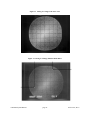
is more "filled in." With radiation flooding the detector, a circular image should be seen.
2.1.7 CHECKING NOISE LEVEL
1. Turn the Model 2401 power OFF. Connect a second oscilloscope, if available, to the "SUM" BNC-type connector
on the rear panel of the Model 2401B. (If a second oscilloscope is not available, the scope monitoring the X-Y signals
above may be used, making sure to turn the units off before disconnecting the Z-axis cable. It is preferable to continue
monitoring the X-Y outputs as well, if possible). Connect the RATE output to the EXT TRIGGER of the oscilloscope
for easiest triggering and set the horizontal SWEEP TIME to 1 sec per division.
2. Turn the HV off. Turn the Model 2401B ON. Approximately 10-15 mV (peak-to-peak) "white" broadband noise
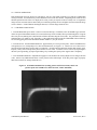
will typically be seen, with perhaps a few line-related transients (see Figure 2.1). About 5-10 mV of this noise is
generated by the RAE and electronics and is not reducible. All such transients should be smaller than 300 mV (peakto-peak), or they will be interpreted by the electronics as real events. Transients can be reduced by improving the
detector system grounding, by improving shielding or by isolating the system power supplies more completely.
3. Leave the Model 2401B ON. Adjust the HV supply to 0 volts and turn ON. Slowly adjust to a low voltage (100-300
volts). Observe any additional transients or noise present on the SUM output. If the HV power supply is properly
filtered and isolated, no change should be seen.
Figure 2.1 SUM Pulse Residual Noise (trailing portion of SUM waveform), 20 mV/cm
(peak-to-peak noise should be less than 10-15 mV, 20 mV maximum)
3300/2400 System Manual
page 32
18 Nov 2013, Rev I
4. Again increase the HV power supply voltage to the correct operating voltage for the MCP/RAE sensor and voltage
divider in use. Turn on a source of countable events (i.e. stray electrons from an operating ion vacuum gauge or a
flashlight bulb filament operating in vacuum at about 50-70% of its rated voltage makes a convenient source if none
is otherwise available). Pulses similar to those shown in Figure 2.2, Analog Sum Pulse Height Distribution, should
be seen at the SUM output. Make minor adjustments in the HV supply voltage until the "mean" (0 to peak) height is
between 1.5 to 2.0 volts without introducing excessive background (see HV Optimization section in this manual). It
is suggested to clearly mark this HV setting on the HV Power Supply as a reminder of the correct operating voltage.
2.1.8 CHECKING SPATIAL RESOLUTION
Spatial resolution and spatial linearity tests can be made on the system by placing a transmission mask, with
appropriate details on it, directly in front of the MCP surface and collecting the data on an appropriate digital data
collection system.
2.2 OPTIMIZING HV BIAS SETTINGS
Spatial resolution is optimized in this type of detector system when the levels of the charge signals from the RAE are
within certain ranges. In turn, these levels are directly related to the gain of the MCP's and thus operating HV bias
voltage.
While these charge levels are too low (typically 10-12 coulombs) to conveniently measure at the RAE, a monitor output
called SUM is provided on most Quantar Technology readout electronics (see Manual for Position Analyzer). The
SUM signal is representative of the total charge deposited on the RAE from the MCP's, regardless of spatial position.
There are several ways to measure the SUM signal and thereby determine if MCP gain is proper. This measurement
is referred to as the Pulse Height Distribution (this is the event-to-event, statistical distribution to the gain particular
events experience as they pass through the MCP stacks).
2.2.1
METHOD 1. INPUT LEVEL METER.
The Model 2401B Position Analyzer is equipped with a front panel meter that monitors the approximate SUM signal
amplitude. Put the Meter Switch in the INPUT LEVEL position. The meter should indicate approximately in the
black band zone on the bottom scale of the meter. Note, at very low count rates, this method is not effective (the meter
needle will swing from zero to full scale erratically). This is the least accurate method yet is useful for routine
monitoring during normal operation.
2.2.2
METHOD 2. OSCILLOSCOPE.
Connect an oscilloscope to the SUM output connector of the Quantar readout electronics. Set the vertical sensitivity
to 1 V/cm and horizontal sweep to 1 sec/cm (Model 2401). Operate the detector with a count rate of approximately
1000 counts per second. By adjusting the trigger control, you will be able to observe the bipolar, shaped pulses from
the shaper amplifier. The average zero-to-positive-peak amplitude should be 1.5 to 2.0 volts. There will be some larger
peak amplitude pulses and some smaller. Adjust the HV bias (observing the maximum of 1000 volts per MCP) to
achieve an average of the proper height. A display of what the waveform should look like is shown in Figure 2.2.
3300/2400 System Manual
page 33
18 Nov 2013, Rev I
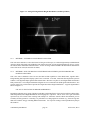
Figure 2.2 Analog SUM Signal Pulse Height Distribution (Oscilloscope Photo)
2.2.3
METHOD 3. EXTERNAL PULSE HEIGHT ANALYZER.
This is the same method as 2. above but instead of using an oscilloscope, use a Pulse Height Analyzer (Multichannel
Analyzer) which will sample each SUM pulse peak, digitize and "bin" it so the exact distribution can be seen. Again,
the centroid of the distribution should be in the 1.5 to 2.0 volt range and the FWHM of the distribution should be 80140% of the mean value (the narrower the better).
2.2.4
METHOD 4. BUILT-IN DIGITAL PULSE HEIGHT ANALYZER IN QUANTAR MODEL 2401
POSITION ANALYZER.
This is the same as Method 3 above but uses the built-in PHA capabilities of the Model 2401, together with a
histogramming data acquisition-display system if one is available. To do this, connect the data acquisition system to
read the Y-axis digitized output signal from the Model 2401. Move the rear-panel Y-Axis Digital Mode Switch to the
PHA position (the Y-axis sample-and-hold and digitizer are now connected to the SUM signal rather than the Y-axis
position signal. The collected data represents the Digital Sum Pulse Height Distribution. A typical digital PHD is
shown in Figure 2.3.
USE OF UV EXCITATION IN PHD MEASUREMENTS.
Depending on photon energy, angle of incidence and other experimental factors, it may not be possible to obtain a fullysaturated (peaked) Pulse Height Distribution when imaging far UV photons. This is due to lower gain sometimes
experienced by UV-excited events resulting from multiple UV reflections down the MCP microchannels prior to
secondary electron generation. Generally, it is preferable to use charged-particle excitation (e.g. electrons of greater
than 100 eV kinetic energy) in making PHD measurements. Use of specific coatings on the input MCP may help in
this situation.
3300/2400 System Manual
page 34
18 Nov 2013, Rev I
Figure 2.3 Typical Digital Histogrammed Pulse Height (Peak Amplitude) Distribution of SUM pulse
(Number of events versus gain of each event)
2.3
METER FUNCTIONS
A selector switch on the Model 2401B front panel allows display of three different operating parameters on the panel
meter.
2.3.1 COUNT RATE
The count rate function indicates, on a log scale, the RATE of incoming pulses. This rate signal is derived from the
look-ahead circuitry which is fed by the "E" preamp. All pulses from this pre-amp greater than 150 mv (referred to
SUM signal) will be included in the rate count even though the position-computing circuitry rejects signals less than
300 mv and greater than 5 volts. This is done to afford the user a better estimate of real input activity. Because this
indication is on a log scale, the meter will indicate offscale to the left for count-rates below 1 count per second.
2.3.2 DEAD-TIME PERCENT
Indicates the percent of incoming events (as measured by RATE signal) that are fully processed to position outputs (as
measured by STROBE signal or X-Y outputs). The inverse of this is percent of incoming events lost.
3300/2400 System Manual
page 35
18 Nov 2013, Rev I
2.3.3 INPUT LEVEL
When operating with a Gaussian distribution of event pulse heights, this function indicates the average input level (size
of charge pulse deposited on RAE by MCP's). A black band spanning the 40% to 60% of full scale range on the meter
indicates the optimum range for this average. It is important to understand how this function is derived. If the incoming
signal is greater than approximately 1.75 volts (1.25 volts in earlier models), the meter is set to full scale until another
pulse come in. If a pulse is less than that value, the meter is set to zero until the next pulse. For high rates of inputs
(greater than 10 Hz) the meter movement averages out these swings into a fairly stable reading. At lower frequencies,
some interpretation will be necessary. At frequencies in the 0 to 5 Hz range, the needle will tend to swing from one
extreme to the other and not necessarily be interpretable. Note that a proper indication is only obtained for inputs with
a distribution of input levels. Note that for constant-amplitude inputs such as those obtained from a pulse generator,
the meter will indicate zero or full value, depending on whether the test pulse amplitude is above or below the MID
threshold.
2.4
EDGE GATING CONTROLS
There are four edge-gating controls located on the front panel of the Model 2401 Position Analyzer. These enable the
user to clip (electronically window) the image independently along the plus and minus X and Y axis directions. This
allows the operator to exclude (veto) portions of the image which are not desired. Note, however, that although these
events are not imaged to the output, because the position of these events is calculated, they do occupy processor time
and therefore contribute to system dead-time.
It is important to note that since these controls overlap in range, it is possible to set them such that the entire image
is blanked. This situation is suspect when the meter indicates normal signal rate and level yet no outputs are observed.
When this occurs set the front-panel Edge Gating controls as follows which will open the edge windows completely:
+Y
-Y
+X
-X
Fully clockwise (to right)
Fully counter-clockwise (to left)
Fully clockwise (to right)
Fully counter-clockwise (to left)
2.5 OPERATING CONSIDERATIONS
2.5.1 COUNT RATE AND DEAD-TIME
In single-event, pulse-counting detector systems, each event is processed serially in time as a separate event. This
implies a processing time or detector system "dead-time" for each event and thus an upper limit on the maximum
number of separate events that can be processed in a given interval of time (counts per second). Furthermore, in most
applications, the arrival of events at the detector are not on a fixed, periodic time spacing but rather arrive with a
randomly-distributed time spacing between events. At low count rates, the processing of a second event is rarely
discontinued due to its arrival too soon after a prior event. As incoming count rates increase, however, increasingly
more events are ignored due to this factor. Finally, at some input count rate, the indicated detector output count rate
goes through a maximum and actually decreases for further increases in incoming rate. At this peak output count rate,
the percentage of input counts that are continuing to be processed will have generally dropped to approximately 40%
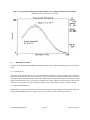
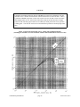
of the incoming rate. This relationship is shown graphically in Figure 2.4, Electronic Dead-Time Curves.
In the Model 2401B, this dead-time is composed of two primary components. In addition, under some circumstances,
there can be a third component associated with the MCP electron multipliers as discussed below.
3300/2400 System Manual
page 36
18 Nov 2013, Rev I
2.5.1.1. Preamp dead-time (3 sec):
The output pulses from the charge-sensitive preamplifiers have a relatively long decay time in order to assure that
complete charge collection occurs from the resistive anode encoder (RAE). This is necessary since the 4 charge signals
from the RAE carry the information regarding spatial position of an event. At high count rates, with a random timespacing between events, this long decay time (tail) can introduce pulse-pileup, where a second pulse is superimposed
on the tail of a preceding pulse. In this case, the amplified pulse is no longer a good measure of charge Q, and this
can lead to errors in determination of spatial position of events. An important objective, therefore, is to ensure that
the amplifier output is restored to the zero baseline prior to processing of the next event.
To minimize this pile-up effect, fast pulse shaping is used to eliminate the long tails from the charge-sensitive amplifier
while the amplitude of the pulse is not significantly affected. This processing reduces the time required to re-establish
the baseline level of the preamps while maintaining desirable pulse amplitude and thus spatial position accuracy and
spatial resolution. In the Model 2401B, this dead-time is approximately 3 microseconds.
This 3 sec dead-time component is paralyzable; this means it is retriggered (restarted) each time a thresholdexceeding event is detected (by the E channel fast preamp) to have reached the charge-sensitive preamplifiers. The
E channel preamp can distinguish separate events providing they are separated in arrival time by at least 400
nanoseconds and their amplitudes exceed a special RATE lower-level threshold.
2.5.1.2. ADC Dead-time
A second dead-time component is due to the finite time required by the analog-to-digital converters (ADC), when this
option is installed, to produce a digitized version of the analog position pulse. During this time period, another event
cannot be processed accurately. The ADC digitization process itself starts 1-2 microseconds after detection of the event
and continues for the following times depending on the digital resolution option installed:
Option 008/EC (8 bit, 256 channel):
Option 009/EE (9 bit, 512 channel):
Option 010/EJ (10 bit, 1024 channel:
2 sec
4 sec
9 sec
In addition, there is some additional overhead time (approximately 0.5-1.0 sec) associated with preparation for the
conversion process and to enable stabilization of circuits in preparation for the next event. The total dead-time for units
with digital output options installed is a combination of the preamp dead-time above and these ADC dead-times. This
results in a total effective dead-time of 4 sec (8-bit), 6 sec (9-bit) and 10 sec (10-bit) per event shown in the
Specifications for these options.
This ADC-related dead-time component is non-paralyzable; it is not re-triggered upon only detection of another event
at the charge-sensitive preamplifier inputs.
2.5.1.3. Dead-time Curves
The combined result of the two dead-time components discussed above regarding the counting rate of the Model 2401B
is shown in Figure 2.4, Electronic Dead-Time Curves, for the analog only version, and 8-bit, 9-bit and 10-bit ADC
option versions. On these plots, the X-Y imaged event rate (measured by the STROBE signal, one pulse for each event
that is fully processed and position-determined) is plotted on the vertical axis and the assumed true input rate (as
measured by the RATE signal and measured by the front-panel meter) is plotted on the horizontal axis. The slight
discontinuity in the digital option dead-time curves at higher count rates is due to the effect of the separate nonparalyzable ADC dead-time component, which enables somewhat higher throughput rates than would be possible if
the ADC component were also paralyzable.
3300/2400 System Manual
page 37
18 Nov 2013, Rev I
CAUTION
It should be noted that monitoring only the STROBE rate signal can be misleading, since the
dead-time curve is double-valued as shown in the dead-time curves referred to above. That is,
a particular STROBE output rate (vertical axis on plot) can occur for both a lower true RATE
and a higher RATE as well. Observation of the input count rate and the direction of output
count rate with increasing input count rate will identify at which point on the curve operation
is taking place. Care must be exercised to avoid inadvertent operation at extremely high count
rates.
Figure 2.4 Electronic Dead-Time Curves, Analog Only and Digital Options
(Assuming no dead-time correction for RATE channel, and random time-of-arrival of events)
3300/2400 System Manual
page 38
18 Nov 2013, Rev I
These dead-times (as indicated by the dead-time curves discussed above and shown in Figure 2.4) combined with the
pulse-pair rejection capability of the Model 2401B, has the overall effect of on the processing of successive events as
follows:
Time Separation T Between Events
Effects On Processing
T < 400 nanoseconds
Events merged into single event with spatial position calculated
as geometric mean. Multiple events within 400 nsec spacing
often are vetoed because they exceed upper level (Overload)
discriminator.
400 nsec < T < 1 sec
Both events are vetoed and eliminated from processing.
1 sec < T < EDT* sec
First event is processed normally, second event is vetoed from
processing and eliminated. *EDT (effective dead-time) depends
on option version; 3-4 sec for analog only, 4 sec for 8 bit, 6
sec for 9 bit, 10 sec for 10 bit.
T > EDT* sec
Both first and second events are processed normally.
2.5.1.4. Dead-time Correction (Live Time-Dead Time).
The approximate dead-time percent (%) can be observed on the front-panel meter when the METER FUNCTION
switch is in the Dead-time position.
In addition, by counting the RATE output (which tracks the occurrence of normal gain events up to approximately 800
KHz to 1 MHz, although with some dead time itself, about 500-600 nsec) relative to the STROBE output (which
outputs a single pulse only for each event that is accepted for processing), the percentage dead-time can be determined.
Many electronic digital frequency counters will calculate the ratio of these two signals automatically using A and B
channels. This percentage can then be used to normalize the imaged, processed count rate data to the true count rate,
thereby compensating for input events that were vetoed by the system from position processing due to potential pulsepileup and consequent inaccuracies. This compensation of position-determined events assumes the dead-time is
uniform over the active area of the detector.
2.5.2. MCP DEAD TIME
In addition to the above electronic (global) dead-time considerations, there are spatially-localized dead-time effects
associated with the MCP's (microchannel plate electron multipliers). These effects are seen only when input event
count rates in a small spatial area exceed the aggregate re-charge time of the group of microchannels involved in the
multiplication process. This effect is dependent on the following factors:
1.
Quiescent, no signal, bias current (also termed "strip current") of specific MCP's used. This determines, in
part, the re-charge time for an individual channel which has fired. The higher the bias current of the MCP
(the lower its resistance), the faster the recharge time.
2.
The spatial dimensions of the input flux to the MCP's (essentially how many individual microchannels are
involved in the multiplication process) and the diameter and spacing of the microchannels in the MCP.
3.
The input count-rate in the localized area.
3300/2400 System Manual
page 39
18 Nov 2013, Rev I
Because of the possible variation in these parameters, it is not possible to give exact predictions of these effects.
However, in general, conventional bias current MCP's have been observed to support a count rate of 50-200 counts per
second per microchannel. This typically leads to effects on observed count-rates only when flux pattern geometries
are considerably smaller than 300 x 300 microns.
If the upper localized MCP count-rate limit is exceeded, effects will first be seen on the localized gain (measured by
the pulse-height distribution) and therefore decreased spatial resolution and then, at somewhat higher count rates, as
a decrease in the STROBE rate. Finally, effects will be seen as a decrease in the RATE signal itself.
2.5.3. MCP GAIN AND BACKGROUNG COUNT RATE
It is valuable to periodically check the electron multiplier (MCP) gain and background count rate. This can be done
most simply by repeating steps outlined in Section 2.2 (Optimizing HV Bias Settings). A slight degradation in gain
as a function of time is to be expected especially in the spatial region on the MCP that is most frequently used. In most
clean, low-flux-rate environments, this amounts to only a few percent a year. Measurement of the digital PHD is the
most accurate method of comparison, noting the HV bias and comparing to prior measurements. If MCP gain
decreases such that the mean gain has moved from the target 1.5 to 2.0 volt range, adjustment of the MCP HV bias
should be made to re-establish the proper gain level.
2.6 SPATIAL RESOLUTION
When the detector is operating at specified spatial resolution, two input peaks of Gaussian-shaped intensity profiles,
spatially-separated by the specified FWHM of the "resolvable element," should be just resolvable (approximately 10%
valley between merged peaks). A statistically significant (1000+) number of counts should be accumulated in the peaks
to make this measurement. This is shown diagrammatically in Figure 2.5, Spatial Resolution. From another
perspective, this "spread" function is simply the "position-jitter" in the electronically-calculated spatial positions of a
large number of events which were incident on the theoretically exact same spatial position on the active sensor surface.
In Figure 2.5, also note the filled dots on the curve which represent the sampled digital data. These digital samples
of the analog position signals are taken at fixed positions across the active diameter of the sensor. Note, because the
digital output is a "sampled" version of the analog position signals, it is important to (spatially) oversample the analog
signal by using an ADC which provides at least 2 digital channels per "resolution elements width." As an example,
a 3300 Series MCP/RAE Sensor with 2 MCP's is capable of electron-optically resolving (at FWHM of the spatial
resolution spread function) 100 elements across either the X or Y active area diameter. Minimum acceptable digital
oversampling requires, therefore, 100 x 2 = 200 digital data points. The 8-bit (256 channel) ADC would, therefore,
be selected; the 9-bit or 10-bit ADC would give even better digital spatial resolution "fidelity", at the expense of
reduced maximum counting rates. Likewise, the 3300 Series MCP/RAE Sensors using 5 MCP's can resolve 400
"elements" across either diameter, so the minimum number of digital channels is 800, and the 10-bit ADC would be
selected.
3300/2400 System Manual
page 40
18 Nov 2013, Rev I
The appropriate number of digital channels to adequately oversample the analog position signal depends to some extent
on the application as well. In applications requiring careful re-construction of line shapes or accurate determination
of peak center locations, such as in some types of spectroscopy, the need is more critical. In other applications, the
need may be less demanding.
Achievement of specified spatial resolution depends primarily on:
1.
Reduction of extraneous noise from being introduced into the system. This can be diagnosed from the SUM
pulse output observed on an oscilloscope.
2.
Adequate gain in the MCP's which assures that the signal levels are sufficiently high relative to thermallygenerated noise such that the jitter in event-to-event position calculations is minimized.
In addition, the user must be careful not to allow aberrations in optics or electron-optics to smear spatial separation
of the input flux prior to reaching the detector.
Observed spatial resolution is a convolution of the detector "spatial-resolution spread function" and the intrinsic spatial
resolution (spread) of the input flux pattern itself. In addition, the measured "spread function" is subject to the usual
statistical uncertainties of counting, which decrease as the number of accumulated counts in the measurement increase.
These independent sources typically add in an RMS manner.
(FWHM)2observed = (FWHM)2input + (FWHM)2det + (FWHM)2statistics
Figure 2.5 Definition of Spatial Resolution (Resolvable Element)
High-Spatial-Resolution Version Performance Shown, 400 x 400 Resolvable Elements, Infinitely-Narrow Input
3300/2400 System Manual
page 41
18 Nov 2013, Rev I
SECTION 3. DIAGNOSTICS AND TROUBLESHOOTING
3.1 PROBLEM DIAGNOSIS AND TROUBLESHOOTING
Operational problems that occur in this type of system must be carefully analyzed to efficiently determine the source
of the problem and enable correction. In this section, a number of possible problem symptoms are described with
possible tests for specific causes outlined in the form of decision trees.
Problems which arise at first turn-on after installation or after re-installation following a period of non-use are often
caused by basic problems involving signal or HV leads, noise pickup, inadequate vacuum or, possibly, hardware failure.
Check these factors carefully.
Use the procedures outlined to determine if the problem is present only when HV is ON or OFF, or if the problem can
be isolated to the MCP/RAE Sensor or to the electronics.
Problems which occur at some point during normal operation (without any changes in wiring, mounting, vacuum, etc)
are generally of a somewhat different type and are more likely to involve hardware failure of some type. However, with
complex experimental situations in UHV systems, do not overlook the possibility that some other factor has, in actual
fact, changed and is causing an observable abnormality at the detector, while the detector itself is operating normally.
Refer to the Model 2401B Operation and Service Manual for detailed Theory of Operation, Component Locators and
Schematic diagrams for the electronic circuits.
When communicating with Quantar Technology Customer Technical Support regarding installation or operational
problems, it is helpful to have answers to as many of the applicable questions in the decision trees as possible.
3300/2400 System Manual
page 42
18 Nov 2013, Rev I
Figure 3.1 Analog X-Y Image, Full Active Area
Figure 3.2 Analog X-Y Image, Emission Point Defect
3300/2400 System Manual
page 43
18 Nov 2013, Rev I
Figure 3.3 Analog X-Y Image, Input Leads Interchanged
Figure 3.4 Analog X-Y Image, One Corner Not Connected Properly
3300/2400 System Manual
page 44
18 Nov 2013, Rev I
Figure 3.5 Analog X-Y Image, Two Opposite Corners Not Connected Properly
Figure 3.6 Digital Image, Incorrect ADC Span and Zero Adjustments
3300/2400 System Manual
page 45
18 Nov 2013, Rev I
Figure 3.7 Troubleshooting Decision Tree, Image on CRT Not Circular
3300/2400 System Manual
page 46
18 Nov 2013, Rev I
Figure 3.8 Troubleshooting Decision Tree, No Output From Detector
3300/2400 System Manual
page 47
18 Nov 2013, Rev I
Figure 3.9 Troubleshooting Decision Tree, Insufficient Number of Events Detected
3300/2400 System Manual
page 48
18 Nov 2013, Rev I
Figure 3.10 Troubleshooting Decision Tree, Background Too High or "Hot Spots"
3300/2400 System Manual
page 49
18 Nov 2013, Rev I
APPENDIX: TECHNICAL REFERENCES
3300/2400 System Manual
page 50
18 Nov 2013, Rev I
Index
ADC Deadtime . . . . . . . . . . . . . . . . . . . . . . . . . . . . . . . . . . . . . . . . . . . . . . . . . . . . . . . . . . . . . . . . . . . . . page 37
ADC Span and Zero, incorrect adjustment . . . . . . . . . . . . . . . . . . . . . . . . . . . . . . . . . . . . . . . . . . . . . . page 45
Background, count rate . . . . . . . . . . . . . . . . . . . . . . . . . . . . . . . . . . . . . . . . . . . . . . . . . . . . . . . . . . . . . . page 32
Background, from ion pumps . . . . . . . . . . . . . . . . . . . . . . . . . . . . . . . . . . . . . . . . . . . . . . . . . . . . . . . . . page 31
Biasing, HV, RAE (anode) . . . . . . . . . . . . . . . . . . . . . . . . . . . . . . . . . . . . . . . . . . . . . . . . . . . . . . . . . . . page 15
Black band, input level meter function . . . . . . . . . . . . . . . . . . . . . . . . . . . . . . . . . . . . . . . . . . . . . . . . . . page 33
Cable, coax . . . . . . . . . . . . . . . . . . . . . . . . . . . . . . . . . . . . . . . . . . . . . . . . . . . . . . . . . . . . . . . . . . . . . . . . page 14
Capacitors . . . . . . . . . . . . . . . . . . . . . . . . . . . . . . . . . . . . . . . . . . . . . . . . . . . . . . . . . . . . . . . . . . . . . . . . page 15
Capacitors, ceramic, HV, chip . . . . . . . . . . . . . . . . . . . . . . . . . . . . . . . . . . . . . . . . . . . . . . . . . . . . . . . . page 15
Capacitors, HV, decoupling . . . . . . . . . . . . . . . . . . . . . . . . . . . . . . . . . . . . . . . . . . . . . . . . . . . . . . . . . . page 15
Ceramic-bead-insulated coax . . . . . . . . . . . . . . . . . . . . . . . . . . . . . . . . . . . . . . . . . . . . . . . . . . . . . . . . . page 14
Coax cable . . . . . . . . . . . . . . . . . . . . . . . . . . . . . . . . . . . . . . . . . . . . . . . . . . . . . . . . . . . . . . . . . . . . . . . . page 14
Coax, ceramic-bead-insulated . . . . . . . . . . . . . . . . . . . . . . . . . . . . . . . . . . . . . . . . . . . . . . . . . . . . . . . . . page 14
Configuration, Front MCP Surface at Ground Voltage . . . . . . . . . . . . . . . . . . . . . . . . . . . . . . . . . . . . . page 23
Configuration, Front MCP Surface at Non-Ground Voltage . . . . . . . . . . . . . . . . . . . . . . . . . . . . . . . . . page 23
Configurations, HV Bias . . . . . . . . . . . . . . . . . . . . . . . . . . . . . . . . . . . . . . . . . . . . . . . . . . . . . . . . . . . . . page 23
Count Rate . . . . . . . . . . . . . . . . . . . . . . . . . . . . . . . . . . . . . . . . . . . . . . . . . . . . . . . . . . . . . . . . . . . . . . . . page 35
Count Rate and Deadtime, relationship between . . . . . . . . . . . . . . . . . . . . . . . . . . . . . . . . . . . . . . . . . . page 36
Current, minimum, voltage divider . . . . . . . . . . . . . . . . . . . . . . . . . . . . . . . . . . . . . . . . . . . . . . . . . . . . . page 19
Customer Technical Support . . . . . . . . . . . . . . . . . . . . . . . . . . . . . . . . . . . . . . . . . . . . . . . . . . . . . . . . . . page 42
Dead-Time Correction (Live Time-Dead Time). . . . . . . . . . . . . . . . . . . . . . . . . . . . . . . . . . . . . . . . . . . page 39
Dead-Time Curves . . . . . . . . . . . . . . . . . . . . . . . . . . . . . . . . . . . . . . . . . . . . . . . . . . . . . . . . . . . . . . . . . . page 37
Dead-Time Percent . . . . . . . . . . . . . . . . . . . . . . . . . . . . . . . . . . . . . . . . . . . . . . . . . . . . . . . . . . . . . . . . . page 35
Deadtime, ADC . . . . . . . . . . . . . . . . . . . . . . . . . . . . . . . . . . . . . . . . . . . . . . . . . . . . . . . . . . . . . . . . . . . . page 37
Deadtime, MCP . . . . . . . . . . . . . . . . . . . . . . . . . . . . . . . . . . . . . . . . . . . . . . . . . . . . . . . . . . . . . . . . . . . . page 39
Decoupling, capacitors, HV . . . . . . . . . . . . . . . . . . . . . . . . . . . . . . . . . . . . . . . . . . . . . . . . . . . . . . . . . . . page 15
Description, General . . . . . . . . . . . . . . . . . . . . . . . . . . . . . . . . . . . . . . . . . . . . . . . . . . . . . . . . . . . . . . . . . page 9
Edge Gating Controls . . . . . . . . . . . . . . . . . . . . . . . . . . . . . . . . . . . . . . . . . . . . . . . . . . . . . . . . . . . . . . . page 36
Electrical Connections, 2 MCP versions, Models 3390 and 3394 . . . . . . . . . . . . . . . . . . . . . . . . . . . . . page 16
Electrical Connections, 5 MCP versions, Models 3391 and 3395 . . . . . . . . . . . . . . . . . . . . . . . . . . . . . . page 17
Emission Point Defect . . . . . . . . . . . . . . . . . . . . . . . . . . . . . . . . . . . . . . . . . . . . . . . . . . . . . . . . . . . . . . . page 43
Feedthroughs, vacuum flange . . . . . . . . . . . . . . . . . . . . . . . . . . . . . . . . . . . . . . . . . . . . . . . . . . . . . . . . . page 15
Final Performance Test Report . . . . . . . . . . . . . . . . . . . . . . . . . . . . . . . . . . . . . . . . . . . . . . . . . . . . . . . page 19
Gain, MCP, re spatial resolution . . . . . . . . . . . . . . . . . . . . . . . . . . . . . . . . . . . . . . . . . . . . . . . . . . . . . . page 19
Gating controls, edge, front panel . . . . . . . . . . . . . . . . . . . . . . . . . . . . . . . . . . . . . . . . . . . . . . . . . . . . . . page 36
Ground loops, minimizing . . . . . . . . . . . . . . . . . . . . . . . . . . . . . . . . . . . . . . . . . . . . . . . . . . . . . . . . . . . . page 18
Holes, clearance, mounting . . . . . . . . . . . . . . . . . . . . . . . . . . . . . . . . . . . . . . . . . . . . . . . . . . . . . . . . . . . page 11
HV Bias, and Spatial Resolution . . . . . . . . . . . . . . . . . . . . . . . . . . . . . . . . . . . . . . . . . . . . . . . . . . . . . . . page 19
HV Bias, Configurations, Choice of . . . . . . . . . . . . . . . . . . . . . . . . . . . . . . . . . . . . . . . . . . . . . . . . . . . . page 23
HV Bias, Optimizing . . . . . . . . . . . . . . . . . . . . . . . . . . . . . . . . . . . . . . . . . . . . . . . . . . . . . . . . . . . . . . . . page 33
HV Divider, current selection . . . . . . . . . . . . . . . . . . . . . . . . . . . . . . . . . . . . . . . . . . . . . . . . . . . . . . . . . page 19
HV Polarity . . . . . . . . . . . . . . . . . . . . . . . . . . . . . . . . . . . . . . . . . . . . . . . . . . . . . . . . . . . . . . . . . . . . . . . page 19
INITIAL TURN-ON AND CHECKOUT . . . . . . . . . . . . . . . . . . . . . . . . . . . . . . . . . . . . . . . . . . . . . . . . page 30
Input Level, Meter . . . . . . . . . . . . . . . . . . . . . . . . . . . . . . . . . . . . . . . . . . . . . . . . . . . . . . . . . . . . . . . . . . page 36
interchanged RAE signals, adjacent channels . . . . . . . . . . . . . . . . . . . . . . . . . . . . . . . . . . . . . . . . . . . . page 44
Ion-type pumps . . . . . . . . . . . . . . . . . . . . . . . . . . . . . . . . . . . . . . . . . . . . . . . . . . . . . . . . . . . . . . . . . . . . page 31
MCP Deadtime . . . . . . . . . . . . . . . . . . . . . . . . . . . . . . . . . . . . . . . . . . . . . . . . . . . . . . . . . . . . . . . . . . . . page 39
Meter, Count Rate function . . . . . . . . . . . . . . . . . . . . . . . . . . . . . . . . . . . . . . . . . . . . . . . . . . . . . . . . . . . page 35
Meter, dead-time percent function . . . . . . . . . . . . . . . . . . . . . . . . . . . . . . . . . . . . . . . . . . . . . . . . . . . . . page 35
Meter, Input Level Function . . . . . . . . . . . . . . . . . . . . . . . . . . . . . . . . . . . . . . . . . . . . . . . . . . . page 33, page 36
3300/2400 System Manual
page 51
18 Nov 2013, Rev I
missing RAE signals, one channel . . . . . . . . . . . . . . . . . . . . . . . . . . . . . . . . . . . . . . . . . . . . . . . . . . . . . . page 44
missing RAE signals, two opposing channels . . . . . . . . . . . . . . . . . . . . . . . . . . . . . . . . . . . . . . . . . . . . . page 45
Mounting hole locations, 25 mm, Model 3390, 3391 . . . . . . . . . . . . . . . . . . . . . . . . . . . . . . . . . . . . . . . page 12
Mounting Hole Locations, 40 mm, Models 3394, 3395 . . . . . . . . . . . . . . . . . . . . . . . . . . . . . . . . . . . . . page 13
Mounting methods, sensor, suggested . . . . . . . . . . . . . . . . . . . . . . . . . . . . . . . . . . . . . . . . . . . . . . . . . . . page 10
Mounting, Sensor Assembly . . . . . . . . . . . . . . . . . . . . . . . . . . . . . . . . . . . . . . . . . . . . . . . . . . . . . . . . . . page 11
Mounting, sensor, from front surface . . . . . . . . . . . . . . . . . . . . . . . . . . . . . . . . . . . . . . . . . . . . . . . . . . . page 11
Mounting, sensor, from rear baseplate . . . . . . . . . . . . . . . . . . . . . . . . . . . . . . . . . . . . . . . . . . . . . . . . . . page 11
Noise level, checking on SUM pulse . . . . . . . . . . . . . . . . . . . . . . . . . . . . . . . . . . . . . . . . . . . . . . . . . . . . page 32
OPERATING CONSIDERATIONS . . . . . . . . . . . . . . . . . . . . . . . . . . . . . . . . . . . . . . . . . . . . . . . . . . . page 36
OSCILLOSCOPE, XY Monitor . . . . . . . . . . . . . . . . . . . . . . . . . . . . . . . . . . . . . . . . . . . . . . . . . . . . . . . page 31
PIN # FUNCTION . . . . . . . . . . . . . . . . . . . . . . . . . . . . . . . . . . . . . . . . . . . . . . . . . . . . . . . . . . . . . . . . . . page 27
Preamp deadtime . . . . . . . . . . . . . . . . . . . . . . . . . . . . . . . . . . . . . . . . . . . . . . . . . . . . . . . . . . . . . . . . . . . page 37
Pressure, vacuum, effect on background . . . . . . . . . . . . . . . . . . . . . . . . . . . . . . . . . . . . . . . . . . . . . . . . page 30
Problem Diagnosis, Troubleshooting . . . . . . . . . . . . . . . . . . . . . . . . . . . . . . . . . . . . . . . . . . . . . . . . . . . . page 42
Problems
circular image cut off by display border . . . . . . . . . . . . . . . . . . . . . . . . . . . . . . . . . . . . . . . . . . page 45
diagonal half circle image . . . . . . . . . . . . . . . . . . . . . . . . . . . . . . . . . . . . . . . . . . . . . . . . . . . . . page 44
diagonal line image . . . . . . . . . . . . . . . . . . . . . . . . . . . . . . . . . . . . . . . . . . . . . . . . . . . . . . . . . . page 45
emission points / hot spots image . . . . . . . . . . . . . . . . . . . . . . . . . . . . . . . . . . . . . . . . . . . . . . . . page 43
high backgound count rate / hot spots . . . . . . . . . . . . . . . . . . . . . . . . . . . . . . . . . . . . . . . . . . . . page 49
hourglass / twisted image . . . . . . . . . . . . . . . . . . . . . . . . . . . . . . . . . . . . . . . . . . . . . . . . . . . . . . page 44
insufficient number of event / low sensitivity . . . . . . . . . . . . . . . . . . . . . . . . . . . . . . . . . . . . . . page 48
no output from detector . . . . . . . . . . . . . . . . . . . . . . . . . . . . . . . . . . . . . . . . . . . . . . . . . . . . . . . page 47
non-circular image on CRT . . . . . . . . . . . . . . . . . . . . . . . . . . . . . . . . . . . . . . . . . . . . . . . . . . . . page 46
Pulse Height Distribution . . . . . . . . . . . . . . . . . . . . . . . . . . . . . . . . . . . . . . . . . . . . . . . . . . . . . . . . . . . . page 33
pusle height analysis . . . . . . . . . . . . . . . . . . . . . . . . . . . . . . . . . . . . . . . . . . . . . . . . . . . . . . . . . . . . . . . . page 34
built-in internal analyzer . . . . . . . . . . . . . . . . . . . . . . . . . . . . . . . . . . . . . . . . . . . . . . . . . . . . . . page 34
external analyzer . . . . . . . . . . . . . . . . . . . . . . . . . . . . . . . . . . . . . . . . . . . . . . . . . . . . . . . . . . . . page 34
REAR PANEL DIGITAL OUTPUT CONNECTOR . . . . . . . . . . . . . . . . . . . . . . . . . . . . . . . . . . . . . . . page 27
References, Technical . . . . . . . . . . . . . . . . . . . . . . . . . . . . . . . . . . . . . . . . . . . . . . . . . . . . . . . . . . . . . . . page 50
Resistor, HV, current limiting . . . . . . . . . . . . . . . . . . . . . . . . . . . . . . . . . . . . . . . . . . . . . . . . . . . . . . . . . page 23
Resolution, Spatial . . . . . . . . . . . . . . . . . . . . . . . . . . . . . . . . . . . . . . . . . . . . . . . . . . . . . . . . . . . . . . . . . . page 40
Resolution, spatial, checking . . . . . . . . . . . . . . . . . . . . . . . . . . . . . . . . . . . . . . . . . . . . . . . . . . . . . . . . . . page 33
Series limiting resistors . . . . . . . . . . . . . . . . . . . . . . . . . . . . . . . . . . . . . . . . . . . . . . . . . . . . . . . . . . . . . . page 23
Signal connections . . . . . . . . . . . . . . . . . . . . . . . . . . . . . . . . . . . . . . . . . . . . . . . . . . . . . . . . . . . . . . . . . . page 14
SIGNAL LEADS AND HV LEADS . . . . . . . . . . . . . . . . . . . . . . . . . . . . . . . . . . . . . . . . . . . . . . . . . . . . page 14
Spatial resolution, checking . . . . . . . . . . . . . . . . . . . . . . . . . . . . . . . . . . . . . . . . . . . . . . . . . . . . . . . . . . page 33
spatial resolution, FWHM . . . . . . . . . . . . . . . . . . . . . . . . . . . . . . . . . . . . . . . . . . . . . . . . . . . . . . page 9, page 40
SUM signal . . . . . . . . . . . . . . . . . . . . . . . . . . . . . . . . . . . . . . . . . . . . . . . . . . . . . . . . . . . . . . . . . . . . . . . . page 33
System Interconnection and Biasing, 2 MCP Sensors, Models 3390 . . . . . . . . . . . . . . . . . . . . page 20, page 21
System Interconnection and Biasing, 5 MCP Sensors, Models 3391 . . . . . . . . . . . . . . . . . . . . . . . . . . . page 22
UV excitation of MCP, effect on PHD measurements . . . . . . . . . . . . . . . . . . . . . . . . . . . . . . . . . . . . . . page 34
Vacuum feedthroughs, types . . . . . . . . . . . . . . . . . . . . . . . . . . . . . . . . . . . . . . . . . . . . . . . . . . . . . . . . . . page 15
Vacuum flanges . . . . . . . . . . . . . . . . . . . . . . . . . . . . . . . . . . . . . . . . . . . . . . . . . . . . . . . . . . . . . . . . . . . . page 15
Vacuum, pressure, effect on background . . . . . . . . . . . . . . . . . . . . . . . . . . . . . . . . . . . . . . . . . . . . . . . . page 30
XY Monitor, connecting . . . . . . . . . . . . . . . . . . . . . . . . . . . . . . . . . . . . . . . . . . . . . . . . . . . . . . . . . . . . . page 31
3300/2400 System Manual
page 52
18 Nov 2013, Rev I