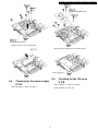
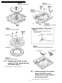
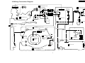
1
Deze download wordt u gratis aangeboden door Pick-upnaalden.nl
Web
:
www.pickupnaalden.com
Email
:
[email protected]
Facebook
:
www.facebook.com/pickupnaalden
Twitter
:
twitter.com/Pickupnaalden
Google+
:
https://plus.google.com/+FCaris_pickupnaalden
ORDER No.AD0404041C0
A2
Direct Drive Digital Turntable
SL-DZ1200PP
SL-DZ1200EB
SL-DZ1200EG
SL-DZ1200EP
SL-DZ1200GN
Colours
(S)..................Silver Type
Specification
● Playable media
CD (12 cm) (5 ” ):
CD-Audio (CD-DA)
CD-R / CD-RW (CD-DA, MP3)
● Headphone
20 mW max. 32 Ω (adjustable)
Output level:
SD Memory Card
● Pickup
● CD-MP3 player format
Compatible compression rate:
Compatible sampling rate:
between 32 kbps and 192 kbps
(Recommended: 128 kbps)
48 kHz / 44.1 kHz / 32 kHz
Compatible sampling rate:
790 nm
Laser Power:
No hazardous radiation is emitted
● General
Power supply:
● SD Audio play format
Audio extension format:
Wave length:
PP ; AC 120 V, 60Hz
EB,EG,EP,GN; AC 220-240 V, 50
Hz
MPEG2-AAC / MP3
48 kHz / 44.1 kHz / 32 kHz
Power consumption:
20 W
Dimensions (W × H × D):
(12 39
● Audio
No. of channels:
2 (stereo)
*
Frequency response :
Output voltage:
Output terminal:
4 Hz-20 kHz
2 Vrms (0 dB) (JEITA)
Pin jack
● Digital audio output
Coaxial digital output:
Mass:
320 × 111 × 330 mm
/ 64 ” × 4 3 / 8 ” × 13 ” )
5.8 kg
(12.8 lb.)
Note:
Specifications are subject to change without notice.
Mss and dimensions are approximate.
*
Specifications are the values when playing CD audio in the CD
PLAYER mode with temporeset.
Pin jack
© 2004 Matsushita Electric Industrial Co., Ltd. All
rights reserved. Unauthorized copying and
distribution is a violation of law.
SL-DZ1200PP / SL-DZ1200EB / SL-DZ1200EG / SL-DZ1200EP / SL-DZ1200GN
CONTENTS
Page
Page
1 Safety Precaution
3
10.4. SW &
2 Caution for AC Mains Lead
4
10.5. LED TEST
LED TEST
3 Handling Precautions for Optical pick-up
36
36
5
10.6. SD SAVE /
3.1. Handling of traverse deck optical pick-up
5
10.7. INITIAL
37
37
3.2. Grounding for electrostatic breakdown prevention
5
10.8. CD UNIT TEST 1
37
LOAD
4 Precaution of Laser Diode
6
5 Accessories
7
11.1. About obtaining the program.
6 Main features
8
11.2. Program Writing to the Flash ROM (IC23) after
7 Component part names
9
11 Cautions after Exchange of the Flash ROM (IC23)
10
8.1. Checking for the control panel (1) P.C.B. and control panel
10
8.3. Checking for the jack P.C.B.
10
8.4. Checking for the power supply P.C.B.
11
8.5. Checking for the CD servo P.C.B.
11
y and motor
8.7. Replacement for the center panel ass ’
y and LCD
42
43
13.1. Schematic Diagram Notes
43
13.2. Schematic Diagram
45
61
14.1. CD SERVO P.C.B. test point table
61
14.2. Printed Circuit Board
63
12
15 Block Diagram
69
13
16 Wiring Connection Diagram
75
17 Terminal Function of ICs
77
17.1. IC2(C2CBHH000043): SYSTEM CONTROL (UI
14
y and slip plate ass ’
y
41
s, Transistors and Diodes
14 Printed Circuit Board
8.8. Replacement for the connection P.C.B. and sensor P.C.b.
8.9. Replacement for the turntable ass ’
40
11.4. Adjusting the Display Contrast
13 Schematic Diagram
8.6. Replacement for the LED P.C.B., loading motor P.C.B.,
CD mouse ass ’
11.3. Program Confirmation
12 Type Illustration of IC ’
10
(2) P.C.B..
8.2. Checking for the main P.C.B.
38
39
Replacement
8 Operation Checks and Component Replacement Procedures
38
Microcomputer)
77
17.2. IC14(C0ZBZ0000910): MULTIMEDIA DIGITAL IMAGE
14
8.10. Replacement for the control panel (2) P.C.B., button base
PROCESSOR (SC Microcomputer)
78
16
17.3. IC34(C0ZBZ0000910): MULTIMEDIA DIGITAL IMAGE
PROCESSOR (MD Microcomputer)
80
16
17.4. IC1(AN8882SB-E1): SERVO AMP.
83
8.12. Replacement for the CD servo P.C.B.
17
17.5. IC102 (C2BBGE000781): SYSTEM CONTROL
83
8.13. Replacement for the optical pick-up
18
B and button base C.
8.11. Replacement for the control panel (1) P.C.B., reverse
switch P.C.B., button base A and button base D
9 Technological Explanation of the Circuit and Signal
10 Self-diagnosis function
18 Replacement Parts List
20
34
85
18.1. Component, Accessory, and Packaging Parts
85
18.2. CD Mechanism Parts
91
10.1. DEVICE TEST
34
19 Cabinet Parts Location
95
10.2. TT BRAKE TEST
35
20 CD Mechanism Parts Location
97
10.3. TT SPEED (Phase) TEST
35
21 Packaging
98
2
SL-DZ1200PP / SL-DZ1200EB / SL-DZ1200EG / SL-DZ1200EP / SL-DZ1200GN
1 Safety Precaution
(This “Safety Precaution” is applied only in U.S.A.)
1. Before servicing, unplug the power cord to prevent an electric shock.
2. When replacing parts, use only manufacturer’s recommended components for safety.
3. Check the condition of the power cord. Replace if wear or damage is evident.
4. After servicing, be sure to restore the lead dress, insulation barriers, insulation papers, shields, etc.
5. Before returning the serviced equipment to the customer, be sure to make the following insulation resistance test to prevent the
customer from being exposed to a shock hazard.
■Insulation Resistance Test
1. Unplug the power cord and short the two prongs of the plug with a jumper wire.
2. Turn on the power switch.
3. Measure the resistance value with ohmmeter between the jumper AC plug and each exposed metal cabinet part, such as screw
heads, control shafts, handle brackets, etc. Equipment with antenna terminals should read between 3MΩ and 5.2MΩ to
allexposedparts. (Fig. A) Equipment without antenna terminals should read approximately infinity to all exposed parts. (Fig. B)
*Note: Some exposed partsmay beisolated from the chassis by design. These will read infinity.
(Fig. A)
(Fig. B)
4. If the measurement is outside the specified limits, there is a possibility of a shock hazard. The equipment should be repaired
and rechecked before it is returned to the customer.
3
SL-DZ1200PP / SL-DZ1200EB / SL-DZ1200EG / SL-DZ1200EP / SL-DZ1200GN
2 Caution for AC Mains Lead
4
SL-DZ1200PP / SL-DZ1200EB / SL-DZ1200EG / SL-DZ1200EP / SL-DZ1200GN
3 Handling Precautions for Optical pick-up
The laser diode in the optical pick-up may break down due to
potential difference caused by static electricity of clothes or
human body.
3.2.2.
Put a conductive material (sheet) or steel sheet on the area
where the optical pick-up is placed, and ground the sheet.
Refer to Fig. 2-3.
So be careful of electrostatic breakdown during repair of the
optical pick-up.
3.1.
Work table grounding
Handling of traverse deck
optical pick-up
1. Do not subject the optical pick-up to static electricity as it is
extremely sensitive to electrical shock.
2. To protect the laser diode against electrostatic breakdown,
short the flexible board (FFC board) with a clip or similar
object. Refer to Fig. 2-1.
Fig. 2-3.
3. Take care not to apply excessive stress to the flexible board
(FFC board).
Caution:
The static electricity of your clothes will not be grounded
through the wrist strap.
4. Do not turn the variable resistor (laser power adjustment). It
has already been adjusted. Refer to Fig. 2-1.
So take care not to let your clothes touch the optical pickup.
Fig. 2-1.
3.2.
3.2.1.
Grounding for electrostatic
breakdown prevention
Human body grounding
Use the anti-static wrist strap to discharge the static electricity
from your body. Refer to Fig. 2-2.
Fig. 2-2.
5
SL-DZ1200PP / SL-DZ1200EB / SL-DZ1200EG / SL-DZ1200EP / SL-DZ1200GN
4 Precaution of Laser Diode
6
SL-DZ1200PP / SL-DZ1200EB / SL-DZ1200EG / SL-DZ1200EP / SL-DZ1200GN
5 Accessories
· AC power supply cord for (PP) area
(REZ1619)....................1 pc.
· AC mains lead for (EB) area
(REZ1496)....................1 pc.
· AC mains lead for (EG),(EP) areas
(REZ1495)....................1 pc.
· AC mains lead for (GN) areas
(REZ1620)....................1 pc.
· Stereo connection cable for all areas
(SFDHBD2N01)....................1 pc.
· Slip surface for all areas
(RGK1704-S2)....................1 pc.
7
SL-DZ1200PP / SL-DZ1200EB / SL-DZ1200EG / SL-DZ1200EP / SL-DZ1200GN
6 Main features
This direct drive digital turntable is designed for DJs to play digital media (CDs and SD audio) giving an analog-like feeling. Having the feeling of an
analog turntable, this unit delivers digitally robust functions and performance realizing a new style of play.
Control panel
SAMPLE PADS
SD CARD LOAD and SAVE
VINYL SIM
•You can store up to 4 audio segments to memory.
•You can use for dual play for up to 2 sample pads,
and use for switching between one shot and loop
play.
You can SAVE and LOAD sample
pad, cue point panel data etc. to
the SD Memory Card.
You can simulate sound similar to an analog player.
DYNAMIC FX
You can transform sound by
using the platter.
CUE PADS
You can store 4 cue points to
memory. Play can be started instantly from one of those cue
points.
FORWARD and REVERSE
The rotation direction of the
platter can be reversed by
switching the play direction
switch to REVERSE or FORWARD.
LOOP play
You can set the IN and OUT
points and play as a loop.
Platter
Play media is synchronized
with platter movement.
Strobo Dot Reflectors
You can use the red strobo illuminator to check changes in
tempo.
Platter slip surface
Use your hand to turn the platter slip surface for scratch,
brake and spin DJ play.
CUE
•Setting the cue point
Store the cue point to
memory.
•Back cue
During play you can instantly
return to the set cue point
and the unit waits in the
pause state.
TEMPO
PLAY SELECT
FREE WHEEL
Selects CD or SD play.
You can switch the platter to
freewheel.
•You can control the play speed
(tempo).
•You can adjust the tempo to
4 levels of settings between
±8 and ±50 using the
RANGE button.
•You can instantly return to
normal playing speed using
the RESET button.
•By using the PITCH LOCK
button the pitch is held even
if the tempo is changed.
Front panel
SD Memory Card slot
CD slot (Slot in type)
Rear panel
TURNTABLE
Mode for DJ play.
CD PLAYER
Mode for use as an audio
player.
8
SL-DZ1200PP / SL-DZ1200EB / SL-DZ1200EG / SL-DZ1200EP / SL-DZ1200GN
7 Component part names
9
SL-DZ1200PP / SL-DZ1200EB / SL-DZ1200EG / SL-DZ1200EP / SL-DZ1200GN
8 Operation Checks and
Component Replacement
Procedures
· This section describes procedures for checking the
operation of the major printed circuit boards and replacing
the main components.
· For reassembly after operation checks or replacement,
reverse the respective procedures. Special reassembly
procedures are described only when required.
8.1.
Checking for the control panel
(1) P.C.B. and control panel (2)
P.C.B..
8.2.
Checking for the main P.C.B.
· Follow the (Step 1) - (Step 3) of item 8.1.
· Check the main P.C.B. (A side) as shown below.
· Check the main P.C.B. (B side) as shown below.
· Check the control panel (1) P.C.B. and control panel (2)
P.C.B. as shown below.
8.3.
Checking for the jack P.C.B.
· Follow the (Step 1) - (Step 3) of item 8.1.
10
SL-DZ1200PP / SL-DZ1200EB / SL-DZ1200EG / SL-DZ1200EP / SL-DZ1200GN
· Check the jack P.C.B. as shown below.
· Check the power supply P.C.B. as shown below.
8.4.
8.5.
Checking for the power supply
P.C.B.
Checking for the CD servo
P.C.B.
· Follow the (Step 1) - (Step 3) of item 8.1.
· Follow the (Step 1) - (Step 3) of item 8.1.
· Follow the (Step 1) of item 8.2.
11
SL-DZ1200PP / SL-DZ1200EB / SL-DZ1200EG / SL-DZ1200EP / SL-DZ1200GN
8.6.
Replacement for the LED
P.C.B., loading motor P.C.B.,
CD mouse ass ’ y and motor
· Follow the (Step 1) - (Step 3) of item 8.1.
· Follow the (Step 1) of item 8.2.
· Follow the (Step 1) - (Step 9) of item 8.5.
12
SL-DZ1200PP / SL-DZ1200EB / SL-DZ1200EG / SL-DZ1200EP / SL-DZ1200GN
8.7.
13
Replacement for the center
panel ass ’ y and LCD
SL-DZ1200PP / SL-DZ1200EB / SL-DZ1200EG / SL-DZ1200EP / SL-DZ1200GN
8.9.
Replacement for the turntable
ass ’ y and slip plate ass ’ y
· Follow the (Step 1) - (Step 6) of item 8.7.
· Follow the (Step 1) - (Step 5) of item 8.8.
8.8.
Replacement for the
connection P.C.B. and sensor
P.C.b.
· Follow the (Step 1) - (Step 6) of item 8.7.
14
SL-DZ1200PP / SL-DZ1200EB / SL-DZ1200EG / SL-DZ1200EP / SL-DZ1200GN
15
SL-DZ1200PP / SL-DZ1200EB / SL-DZ1200EG / SL-DZ1200EP / SL-DZ1200GN
8.10. Replacement for the control
panel (2) P.C.B., button base B
and button base C.
· Follow the (Step 1) - (Step 3) of item 8.1.
8.11. Replacement for the control
panel (1) P.C.B., reverse
switch P.C.B., button base A
and button base D
· Follow the (Step 1) - (Step 3) of item 8.1.
16
SL-DZ1200PP / SL-DZ1200EB / SL-DZ1200EG / SL-DZ1200EP / SL-DZ1200GN
8.12. Replacement for the CD servo
P.C.B.
· Follow the (Step 1) - (Step 3) of item 8.1.
· Follow the (Step 1) of item 8.2.
· Follow the (Step 1) - (Step 9) of item 8.5.
· Follow the (Step 1) - (Step 4) of item 8.6.
17
SL-DZ1200PP / SL-DZ1200EB / SL-DZ1200EG / SL-DZ1200EP / SL-DZ1200GN
8.13. Replacement for the optical
pick-up
· Follow the (Step 1) - (Step 3) of item 8.1.
· Follow the (Step 1) of item 8.2.
· Follow the (Step 1) - (Step 9) of item 8.5.
· Follow the (Step 1) - (Step 4) of item 8.6.
· Follow the (Step 1) - (Step 5) of item 8.12.
18
SL-DZ1200PP / SL-DZ1200EB / SL-DZ1200EG / SL-DZ1200EP / SL-DZ1200GN
· Grease PART NO.: RFKXPG641
19
SL-DZ1200PP / SL-DZ1200EB / SL-DZ1200EG / SL-DZ1200EP / SL-DZ1200GN
9 Technological Explanation of the Circuit and Signal
Composition of the parts: (Refer to the block diagram, Fig. 1)
POWER (power supply), JACK, MAIN, panel, motor (turntable), CD unit, LCD unit
Outline of the parts: (Refer to the block diagram, Fig. 1)
1. POWER (power supply) (Fig. 9)
SW power supply with multiple correspondence from 100 to 240 V
AC inlet and fuse differ according to the destination (the constants are used in common).
Output of +20 V, +15 V, +7 V, +5 V, +3.3 V, -15 V
Power supply for +20 V motor
Power supply for +15 V analog operation amplifier
Power supply for -15 V analog operation amplifier, power supply for LCD
Power supply for +7 V CD unit motor
+5 V system power supply
+3.3 V system power supply
+1.8 V system power supply (generated at the MAIN circuit board)
2. JACK
Composed of I/O JACK, SW, turntable drive circuit, analog circuit, etc.
Headphone JACK: 6.3 mm specification, stereo, 20 mW (at the time of a 32 ohm load)
Headphone volume: Variable
LINE OUT: RCA pin type, L/R ch
Digital output: COAXIAL
Control: Used with connection of stereo MINI, DZ, or MZ
Mode switching switch: Turntable mode (scratching is possible, turntable speed)
CD mode (scratching is not possible, the turntable does not turn)
Brake: The brake at the time of turntable mode becomes variable.
3. MAIN
System control is performed.
Composed of the three microcomputers UI, SC, and MD.
UI microcomputer: Control of the main panel
SC microcomputer: Mainly control of sound processing, LCD display, audio output
MD microcomputer: Mainly control of data reading, CD and SD data reading
4. Panel
Composed of switches, LEDs, adjustment controls, etc.
Panel switches, LED control, volume control
A/D method by resistance division, divided into 10 steps
5. Motor
This is the turntable motor circuit board.
It is composed of the motor common with SL1200.
6. CD unit
CD drive unit for CAR, with antivibration construction, max. 4x speed.
The MAIN circuit board uses an ATAPI connection.
7. LCD unit
This is a display LCD unit with 128 x 128 full dots and blue mode.
Explanation of the main signals:
UI microcomputer
• Panel control
SW10 to 40: SW input
SW input for SD open detection, CD/turntable switching, and switches other than
EJECT
CD/SD: CD/SD switching input
REV: Reverse switch input
PCON: Pitch control switch input
CP0, 1, CPLED, CPDATA, CPCLK: LED control
STROBE: Stroboscope output
20
SL-DZ1200PP / SL-DZ1200EB / SL-DZ1200EG / SL-DZ1200EP / SL-DZ1200GN
• Others
ENCA/B: Sensor encoder input
LINKSD/LINKSK: For control terminals
TTPWM: Turntable clock
SC microcomputer
• Audio output
DSP.DATA/BCK/LRCK/SCK: Audio data, digital output data
• LCD controls
CRDT0 to 7, others
• CD shutter controls
CDOPN/CLS, CDSMO/C: CD shutter detection and motor control
• JTAG.xx: For bug check
• DSP.DTx, GIOx: For MD microcomputer communication
MD microcomputer
• SRDT0 to 15, Others: For communication with the CD unit and for communication with SDI/F
Signal flow:
1. Panel (refer to the block diagram, Fig. 2)
Input signals from CP1, CP2, CP3, CP5, PCON
Input to the A/D input port of the UI microcomputer
LED output and execution of communication with SC
LCD display, audio output, turntable rotation, etc.
2. LED (refer to the block diagram, Fig. 3)
Port output from the UI microcomputer (from data of the above switches etc.)
Data output to CP1, CP3, CP5, STROBE, etc.
Address serial data are concerted to the matrix and LEDs are lit.
3. Audio flow for CD, SD (refer to the block diagram, Fig. 4/5)
CD unit
SD slot
MD microcomputer <--> SDRAM
SD I/F
Data storage
SC microcomputer <-- UI microcomputer <-- Slip sensor
Audio processing <--> SDRAM
Sensor, tempo, REV, FREE
DAC/DIT
Audio output
4. Turntable (turntable mode) (refer to the block diagram, Fig. 6)
Switch input
UI microcomputer
<-- Clock, reverse, start/stop, free-wheel
Motor control IC
Driver IC
Motor
<-- Turntable rotation
21
SL-DZ1200PP / SL-DZ1200EB / SL-DZ1200EG / SL-DZ1200EP / SL-DZ1200GN
5. LCD (refer to the block diagram, Fig. 7)
Switch input
UI microcomputer
SC microcomputer <-- Acquisition of display data
LCD
6. Reset circuit (refer to the block diagram, Fig. 8)
Reset circuits exist for +5 V, +3.3 V, and +1.8 V, and the operation is independent in regard
to the circuit boards.
In the end, +3.3 V performs overall control.
22
SL-DZ1200PP / SL-DZ1200EB / SL-DZ1200EG / SL-DZ1200EP / SL-DZ1200GN
DZ1200 system block diagram
Fig 1
LINK
LINE OUT
H.PHONE DIGITAL
OUT
OUT
Refer to the item "Composition of the parts".
Refer to the item "Outline of the parts".
Refer to the item "Explanation of the main signals".
JACK
MUTE
Turntable
AMP
Motor
Controller AN6680
Driver AN6675
Sensor
AMP
BUFFER
POWER
VCC
Switching power supply
AC100V~240V
MAIN
DAC
PCM1734
DIGITAL
TC9271
VCC
4.5 V monitoring
27MHz
11.29MHz
Microcomputer
RESET
M30622
27MHz
DSC25
DSC25
(SC microcomputer)
(MD microcomputer)
Serial
Serial
(UI microcomputer)
16MHz
I2C
EEROM
ADC IN
2.9 V monitoring
RESET
External bus
Buffer
FLASH
ROM
External bus
SDRAM
X2
Buffer
FLASH
ROM
SDRAM
SD I/F
MN5772
(ATAPI interface)
CP
TEMPO VR
Shutter
LCD
Decoder
CD
SD
LED
SW
SW
LED
LED
DZ1200 SW, VOLUME input circuit block diagram
Refer to the item "Signal flow", panel.
Fig 2
MAIN
CP1
CP3
IC2
UI microcomputer
M30622
CP2
A/D
input
SW10~40
SW x6
A/D
input
A/D
input
A/D
input
CD/SD
SW x9
SW x8
SW x3
CD/SD
SW
DE
REV
CP5
SW x5
SW x4
P-CON
Scratch microcomputer
DSC25
REV SW
DE
DE
PCON
Serial
communication
IC14
SW x4
TEMPO
VR
DE
23
SL-DZ1200PP / SL-DZ1200EB / SL-DZ1200EG / SL-DZ1200EP / SL-DZ1200GN
24
SL-DZ1200PP / SL-DZ1200EB / SL-DZ1200EG / SL-DZ1200EP / SL-DZ1200GN
DZ1200 audio output circuit block diagram
Refer to the item "Signal flow", CD, SD audio flow.
Fig 5
MAIN
JACK
IC18
+7 V power supply
Three-terminal
+5 V for audio
regulator
IC14
IC33
DAC
Scratch microcomputer
PCM1734
DSC25
LRCK
DATA
BCK
Analog
audio
IC35
Operation
amplifier
M5218A
Analog
audio
IC2004
Operation
amplifier
M5218A
Analog
audio
IC2002
Operation
amplifier
M5218A
Q2004
Q2005
Q2006
Q2007
H.PHONE
audio
T2001
Isolation
Digital
audio
LINE
OUT
SCK
Serial communication
VR2002
Digital output enable signal
H.PHONE
VR
H.PHONE
OUT
IC2
UI microcomputer
M30622
MUTE signal
X6
IC4
DIGITAL
AUDIO
TC9271
11.2896MHz
IC15
Gate
7W08F
Digital
audio
MUTE
circuit
IC2006
7WU04F
Buffer
transformer
DZ1200 turntable control circuit block diagram
Refer to the item "Signal flow", turntable.
Fig 6
MAIN
JACK
Turntable
+20V
+10V
Q2008
+20 V power supply
Transistor
Clock
IC2003
Motor controller
AN6680
IC2
Serial
M30622
X2001
communication
Motor
TT.PWM
UI microcomputer
IC2005
Motor driver
AN6675
Three-phase signal
4.193MHz
Brake
ECR
adjustment
VR2001
Torque switching
EC
IC2007
IC2008
Q2009
FG
AMP
Analog SW
IC14
Scratch microcomputer
DSC25
DIGITAL
OUT
Motor ON/OFF
Turntable FREE
Forward/reverse switching signal
25
FG signal
FD coil
SL-DZ1200PP / SL-DZ1200EB / SL-DZ1200EG / SL-DZ1200EP / SL-DZ1200GN
DZ1200 LCD access circuit block diagram
Refer to the item "Signal flow", LCD.
Fig 7
LCD unit
MAIN
Data bus
IC9
IC14
Voltage conversion
Scratch microcomputer
LVX4245
Data bus
DSC25
Controller
IC1, 19
Control bus
Control bus
Voltage conversion
+5V
+5 V power supply
Operation power supply
Contrast
PWM
voltage control
Contrast power supply
-10~ -13V
IC23
FLASH
ROM
-15 V power supply
Image data
IC8
Backlight power supply
Three terminal
+5V
+7V
regulator
DZ1200 reset circuit block diagram
Refer to the item "Signal flow", reset circuit.
Fig 8
+1.8V
+3.3V
IC14
Scratch microcomputer
DSC25
RESET
+3.3 V power supply
+1.8V
+3.3V
IC34
Media microcomputer
DSC25
GIO
RESET
IC11
+2.9V
monitoring IC
IC20
+1.8 V power supply
Three-terminal
IC10
+1.6V
regulator
monitoring IC
General purpose output
DE
+5 V power supply
Q5
IC6
+4.5V
monitoring IC
RESET
+5V
IC2
UI microcomputer
M30622
26
SL-DZ1200PP / SL-DZ1200EB / SL-DZ1200EG / SL-DZ1200EP / SL-DZ1200GN
DZ1200 POWER circuit board power supply circuit block diagram
Refer to the item "Outline of the parts", POWER (power supply).
Fig 9
POWER
AC input
100~240V
S1101
Power supply switch
F1101
FUSE
L1120
L1121
Line filter
D1140
Rectifier
diode
T1150
Switching
D1403
Diode
-15V
transformer
1.6A
IC1150
Switching IC
MR1722
D1271
Diode
Q1200
IC1200
Photocoupler
Voltage detection
D1261
Diode
+20V
+7V
IC1302
Three-terminal
+5V
regulator
IC1410
Switching
+3.3V
regulator
IC1201
Three-terminal
regulator
27
+15V
SL-DZ1200PP / SL-DZ1200EB / SL-DZ1200EG / SL-DZ1200EP / SL-DZ1200GN
Fault mode analysis: (Refer to the table of fault symptoms and countermeasures.)
1. The power cannot be switched on.
The power cannot be
switched on.
Replace the fuse.
Does the fuse
blow when the
power is
switched on?
No
Blown fuse
Yes
Defective parts around IC1150, D1140
2. The power can be switched on, but there is no operation.
The power can be switched on, but there is
no operation.
Switch on the power.
Does the LED
of the CD
mouse light?
No
Defective power supply
circuit of the +5 V system
The LCD backlight
lights, but the LED
does not light.
Yes
No
Defect related to the
SC/MD microcomputer
Yes
Do some of the panel
switches/LEDs
operate?
No
Defect related to the UI
microcomputer
Defect related to the UI
microcomputer
Yes
Defect related to the
SC/MD microcomputer
** Observe the waveforms of microcomputer CS, address, and data, and determine the fault location.
When there is absolutely no operation, doubting the SC/MD microcomputer is fastest.
28
SL-DZ1200PP / SL-DZ1200EB / SL-DZ1200EG / SL-DZ1200EP / SL-DZ1200GN
3. Display-related
No LCD display
Can CD audio
etc. be heard?
No
Defect related to the SC
microcomputer
Yes
There is the possibility of a defective
connection in the LCD wiring.
The LED does not
light.
Is the operation of
all switches without
problems?
No
Defect related to the UI
microcomputer
Yes
There is the possibility of a defective
intermediate connection.
4. CD-related
The CD is not
recognized.
Defect related to the
SC/MD microcomputer
Defective intermediate
connection
The CD cannot be ejected.
Defective EJECT SW
Defective power supply
circuit
Defective shutter operation
Defective intermediate
connection
Defective shutter
switch
5. SD-related
The SD is not
recognized.
Defective SD
connector
Defective CD unit
Defective MD
microcompute
Defective I/F IC
29
Defective shutter
motor
SL-DZ1200PP / SL-DZ1200EB / SL-DZ1200EG / SL-DZ1200EP / SL-DZ1200GN
6. Turntable-related
Defective rotation
Defective motor
controller IC
Defective motor driver
IC
Confirmation of the
MAIN control signal
There is rotation, but no
sound.
Can sound be
heard in CD
mode?
No
Yes
Defective turntable
sensor part
Is the LCD TIME
display moving?
No
Defect related to the
SC/MD microcomputer
Yes
Defective audio circuit
7. Related to the audio output
AD signal output is not
possible.
Defective DAC IC
Defective operation
amplifier power supply
Defective MUTE circuit
Analysis points:
1. There are three microcomputers.
The panel operates when UI is running.
When the LED of the PAD button flashes when "REALTIME REC" is pressed while the power is on, SC also is OK.
2.
3.
4.
5.
6.
7.
MD also is OK when updating from SD is possible.
SC/MD operation judgment and sensor judgment can be made by turntable/CD mode switching.
Confirm the power supply if the system is unstable.
Use test mode.
As the panels are connected in the order of CP1 --> CP5 --> CP3, confirm the preceding one.
For analog trouble, confirmation with a test CD (sine wave) is faster as the circuit is simple.
8. CD and SD have different connections to the MD microcomputer, but the signal flow after the input is in common.
30
SL-DZ1200PP / SL-DZ1200EB / SL-DZ1200EG / SL-DZ1200EP / SL-DZ1200GN
Table of fault symptoms and countermeasures (for repair)
** The following fault symptoms assume that a product which operated perfectly at the time of shipping has become defective.
Symptom
Individual symptom
Possible causes
Defect location, countermeasures
1 Related to the
The power cannot be switched on at all. Blown fuse
Replace the fuse on the POWER circuit board.
None
of
the
power
supplies
is
put
out.
IC1150
and
D1140 on the POWER circuit board and
power supply
their surroundings
Each power supply is normal, but there
is no operation.
+1.8 V is not put out.
IC20 and D2 on the MAIN circuit board and their
surroundings
Check that +1.8 V is applied to C13 on the MAIN circuit
board.
The +3.3 V power supply is not put out.
IC1410 and L1271 on the POWER circuit board and
their surroundings
POWER circuit board fuse protector FP1400
The +5 V power supply is not put out.
IC1302 and D1261 on the POWER circuit board and
their surroundings
Check that +5 V is applied to C15 on the MAIN circuit
board.
The +7 V power supply is not put out.
POWER circuit board D1261
Check that +7 V is applied to C19 on the MAIN circuit
board.
The +15 V power supply is not put out.
IC1201 on the POWER circuit board and its
surroundings
Power circuit board resistor R1211
The +20 V power supply is not put out.
D1271 on the POWER circuit board and its
surroundings
The -15 V power supply is not put out.
D1403 on the POWER circuit board and its
surroundings
Microcomputer-related defect
IC2, IC14, and IC34 on the MAIN circuit board and their
surroundings
Defective connection between MAIN-JACK
Confirmation of the connection cable
circuit board and POWER-JACK circuit board Pay attention to the orientation.
Defective oscillation circuit
X1, X3, X5 on the MAIN circuit board and their
surroundings
Confirm that X1 oscillates at 8 MHz and X3 and X5 at
27 MHz.
Defective reset circuit
IC6 and IC11 on the MAIN circuit board and their
surroundings
Output of +5 V for the output of IC6 on the MAIN circuit
board and output of +3.3 V for the output of IC11
Memory-related defects
IC23, IC24, IC25, IC36, and IC38 on the MAIN circuit
board
2 Display-related
Nothing is displayed on the LCD.
Defective connection between MAIN and LCD Connection confirmation, connecting cable replacement
relay circuit board
Defective connection between relay circuit
board and LCD
Defective LCD control circuit
Defective contrast -15 V power supply
Defective LCD unit
Defective microcomputer on the scratch side
Dark LCD
Defective backlight power supply
Defective backlight LED in the LCD
Wire break in the FFC cable of the LCD
circuit board
The LCD display shows incorrect
characters.
Some or all LEDs do not light.
Connection confirmation, FFC cable replacement
IC1, IC9, and IC13 on the MAIN circuit board and their
surroundings
IC12, Q7, and Q8 on the MAIN circuit board and their
surroundings
Confirm that approximately -10 V to -13 V is put out to
C6 on the MAIN circuit board.
Replacement of the LCD unit
IC14 on the MAIN circuit board and its surroundings
IC8 on the MAIN circuit board and its surroundings
Confirm that +5 V is put out for the output of IC8.
Replacement of the LCD unit
Replacement of the LCD unit or the FFC cable
Defective connection between relay circuit
board and LCD
Connection confirmation, FFC cable replacement
Defective LCD control circuit
IC1, IC9, and IC13 on the MAIN circuit board and their
surroundings
Defective LCD unit
Replacement of the LCD unit
Defective LED parts
Defective connection between MAIN and CP
Defective connection between CP1 and CP3
Defective connection between CP1 and CP5
Defective LED decoding circuit on the CP
circuit board
Replacement of the respective LEDs
Connection confirmation, FFC cable replacement
Connection confirmation, FFC cable replacement
Connection confirmation, cable replacement
IC3101, IC3102, IC3103, IC3104, Q3101, Q3102,
Q3103, and Q3104 on the CP circuit board and their
surroundings
Defective operation of the UI microcomputer
IC2 on the MAIN circuit board and its surroundings
31
SL-DZ1200PP / SL-DZ1200EB / SL-DZ1200EG / SL-DZ1200EP / SL-DZ1200GN
Symptom
3 CD-related
Individual symptom
CD loading is not possible.
CD ejection is not possible.
The CD is not recognized correctly.
Possible causes
Defective +7 V CD motor power supply
Defect location, countermeasures
Confirmation of the +7 V power supply of the POWER
circuit board
Check that approx. +7 V is applied to C19 on the MAIN
circuit board.
Defective CD unit
CD unit replacement
Defective wiring of the CD eject button
Confirmation of the wiring between MAIN and CDOPSW
circuit board
Confirmation of the wiring between CDOPSW circuit
board and EJECT circuit board
Defective wiring between MAIN and CD unit
Connection confirmation, FFC cable replacement
Defective wiring between MAIN and CD unit
Defective CD control signal
Connection confirmation, FFC cable replacement
IC3, IC5, IC21, IC22, IC27, and IC29 on the MAIN
circuit board and their surroundings
IC34 on the MAIN circuit board and its surroundings
CD unit replacement
Defective media microcomputer
Defective CD unit
4 SD-related
The CD does not turn.
Defective +7 V CD motor power supply
Confirmation of the +7 V power supply of the POWER
circuit board
Check that approx. +7 V is applied to C19 on the MAIN
circuit board.
Defective CD unit
CD unit replacement
The shutter does not open and close.
Defective shutter motor
Defective motor drive circuit
Shutter motor and its surroundings
Q2, Q3, Q10, and Q11 on the MAIN circuit board and
their surroundings
Defective connection between MAIN and
CDOPSW circuit board
Confirmation of the wiring between MAIN and CDOPSW
circuit board
Confirmation of the wiring between CDOPSW and motor
The shutter motor operates
continuously.
Defective shutter open/close detection switch Defective SW2301, SW2302 on the CDOPSW circuit
board
Recording of CD title information is not
possible.
Defective record EEROM
IC16 on the MAIN circuit board and its surroundings
No recognition
Defective SD lid open/close detection switch
Defective SD I/F IC
SW1 on the MAIN circuit board and its surroundings
IC17 and CN4 on the MAIN circuit board and their
surroundings
SD key rewriting
Defective SD key writing
Reading is not possible.
Defective SD I/F IC
Defective operation of the microcomputer on
the media side
5 Turntable-related
No turning
Unwanted rotation at the time of power
supply start
IC17, CN4, and Q4 on the MAIN circuit board and their
surroundings
IC34 on the MAIN circuit board and its surroundings
Defective connection between MAIN and
JACK circuit board
Connection confirmation, FFC cable replacement
Pay attention to the orientation.
Defective connection between JACK and
MOTOR circuit board
Connection confirmation, cable replacement
Defective motor control IC
IC2003 and IC2005 on the JACK circuit board and their
surroundings
Defective rotation pulse output
IC2 and CN7 on the MAIN circuit board and their
surroundings
JACK circuit board IC2003
Defective motor start signal output
IC2 and CN7 on the MAIN circuit board and their
surroundings
JIC2003 and Q2010 on the JACK circuit board and their
surroundings
Defective motor
Motor circuit board replacement
Defective +3.3 V microcomputer power supply Confirmation of the +3.3 V power supply of the POWER
circuit board
Check that +3.3 V is applied to C14 on the MAIN circuit
board.
Defective connection between MAIN and
JACK circuit board
Connection confirmation, FFC cable replacement
Pay attention to the orientation.
Forward/reverse switching is not
possible.
Defective switching signal
Q2003 on the JACK circuit board and its surroundings
Defective connection of the forward/reverse
switch
Confirmation of the connection between CP2 and CP3
Bad brake effectiveness
Defective motor control IC
IC2003 and IC2005 on the JACK circuit board and their
surroundings
The turntable turns, but no audio is
heard.
Defective rotation detection sensor
SENSOR circuit board SENSOR replacement
Confirm lighting of the SENSOR LED.
Defective connection between SENSOR and
relay circuit board
Connection confirmation, cable replacement
Defective rotation detection FG circuit
IC2003 and Q2009 on the JACK circuit board and their
surroundings
Defective motor control IC
IC2003 and IC2005 on the JACK circuit board and their
surroundings
Irregular rotation
Vacillation of the stroboscope with -50% Defective motor torque switching circuit
slow rotation
32
IC2007, IC2008, Q2019, and Q2020 on the JACK circuit
board and their surroundings
SL-DZ1200PP / SL-DZ1200EB / SL-DZ1200EG / SL-DZ1200EP / SL-DZ1200GN
Symptom
6 Output-related
Individual symptom
No audio output for LINE OUT and
headphone
Possible causes
Defective +15 V, -15 V power supply
Defective MUTE circuit
Distorted output to LINE OUT and
headphone
Defect location, countermeasures
Confirmation of +15 V and -15 V power supply on the
POWER circuit board
Q2001, Q2002, Q2012, Q2013, Q2014, Q2015, Q2016,
Q2017, and Q2018 on the JACK circuit board and their
surroundings
Defective audio DAC
IC33 and IC18 on the MAIN circuit board and their
surroundings
Confirm that +5 V is put out for the output of IC18.
Defective audio amplifier
Defective audio clock circuit
IC35 on the MAIN circuit board and its surroundings
X6 and IC32 on the MAIN circuit board and their
surroundings
Confirm that 11.2989 MHz is oscillated.
Defective +15 V, -15 V power supply
Confirmation of +15 V and -15 V power supply on the
POWER circuit board
IC18 on the MAIN circuit board and its surroundings
Defective three-terminal regulator for the
audio DAC
No sound from LINE OUT L, R
Defective LINE OUT amplifier
IC2004 on the JACK circuit board and its surroundings
No sound from LINE OUT L
Defective Lch MUTE circuit
Defective LINE OUT amplifier
Q2016 on the JACK circuit board and its surroundings
IC2004 on the JACK circuit board and its surroundings
No sound from LINE OUT R
Defective Rch MUTE circuit
Defective LINE OUT amplifier
Q2015 on the JACK circuit board and its surroundings
IC2004 on the JACK circuit board and its surroundings
No sound from the headphone or low
volume
Defective headphone amplifier
IC2002, Q2004, Q2005, Q2006, and Q2007 on the
JACK circuit board and their surroundings
No sound from the left headphone
Defective Lch MUTE circuit
Defective headphone amplifier
Q2018 on the JACK circuit board and its surroundings
IC2002, Q2004, and Q2005 on the JACK circuit board
and their surroundings
No sound from the right headphone
Defective Rch MUTE circuit
Defective headphone amplifier
Q2017 on the JACK circuit board and its surroundings
IC2002, Q2006, and Q2007 on the JACK circuit board
and their surroundings
No digital output (there is analog output) Defective digital audio IC
Defective digital output circuit system
IC4 on the MAIN circuit board and its surroundings
IC15 on the MAIN circuit board and its surroundings
IC2006 on the JACK circuit board and its surroundings
Defective digital IC modification (initial
product)
Confirmation of the GND connection of P10, P23, and
P24 on the IC4 MAIN circuit board
There is digital output, but copying is not Defective digital IC modification (initial
possible.
product)
Confirmation of the GND connection of P10, P23, and
P24 on the IC4 MAIN circuit board
Large shock sound at the time of power Defective MUTE circuit
ON/OFF
Q2001, Q2002, Q2012, Q2013, Q2014, Q2015, Q2016,
Q2017, and Q2018 on the JACK circuit board and their
surroundings
7 Switch- and button- No reaction from any switch or button
related
Defective operation of the UI microcomputer
IC2 on the MAIN circuit board and its surroundings
Defective connection between MAIN and CP1 Connection confirmation, FFC cable replacement
No reaction of LCD panel buttons
Defective operation of the UI microcomputer IC2 on the MAIN circuit board and its surroundings
Defective connection between MAIN and CP1 Connection confirmation, FFC cable replacement
Defective connection between CP1 and CP3
Defective connection between CP1 and CP5
No reaction by a specific button
Defective operation of the UI microcomputer IC2 on the MAIN circuit board and its surroundings
Defective connection between MAIN and CP1 Connection confirmation, FFC cable replacement
Defective connection between CP1and CP3
Defective connection between CP1and CP5
8 Link operation
No link operation
Connection confirmation, FFC cable replacement
Connection confirmation, cable replacement
Connection confirmation, FFC cable replacement
Connection confirmation, cable replacement
Defective operation of the UI microcomputer
IC2 on the MAIN circuit board and its surroundings
Defective diode parts
Replacement of D2004, D2005, D2006, and D2007 on
the JACK circuit board
33
SL-DZ1200PP / SL-DZ1200EB / SL-DZ1200EG / SL-DZ1200EP / SL-DZ1200GN
10 Self-diagnosis function
· Start by switching on the power while pressing EXECUTE, SAMPLE PAD3 for the finished product.
Select the following pages with the buttons (||<< and >>||) at the lower part of the LCD.
10.1. DEVICE TEST
· Press the [TEST] button: ROM/RAM/E2PROM diagnosis and CD/SD interface diagnosis is performed and OK/NG is displayed
on the LCD.
ROM/RAM shows the ROM/RAM contents of SC&MDadded outside the microcomputer. CD/SD means sending a signal to the
unit and receiving an answer.
· Insert a CD: The first title of the CD automatically starts to play. →Signal confirmation at LINE OUT.
· Press the start button with a CD inserted or after inserting a CD. Perform TT forward with tempo ±0. →Visually confirm that the
stroboscope is stopped.
· All LEDs flash with entry to this page. Return to normal condition by real-time REC button operation or escape to page 1.
34
SL-DZ1200PP / SL-DZ1200EB / SL-DZ1200EG / SL-DZ1200EP / SL-DZ1200GN
10.2. TT BRAKE TEST
· Set the brake to the maximum for FAST and press the start button with a CD inserted. (Please Wait is displayed for some time.)
Press the [FAST] button when steady rotation has been reached. →The TT count from pressing [FAST]until complete stop is
measured and the value is displayed on the LCD.
Next, set to the maximum for SLOW, press the start button, and then press the [SLOW] button in the same way to display the
respective results on the LCD. (SLOW inspection ispossible only after FAST has been performed once.)
Judgment standard: [FAST] Within 80 degrees (TT count values 15858) OK, [SLOW] Angle difference from FAST within 60
degrees (count value 11894 or more) OK
· Tempo reset is done automatically with entry to this page.
10.3. TT SPEED (Phase) TEST
· Press the start button with a CD inserted, move the tempo slider sequentially to 0, +50%, and -50%, and press [TEST].
(Perform this operation manually. This also serves for inspection of the slider itself).At this time, automatic counting is
performed on the inside (a measuring time of TT 1.5 revolutions each is required), and when the upper and lower limit range
set in advance is not exceeded, OK is displayed on the LCD, while NG is displayed when therange is exceeded → Phase
deviation (DP value) within 12 between MAX and MIN.
Note:
For the measuring of page 3, it is required to wait until the TT speed has stabilized before the [TEST] button is pressed.
· At the same time, the cogging deviation width also is displayed on the LCD. (OK/NG display also is performed if upper and lower
limit have been decided.)
· When the tempo slider is not set to ±50% or 0% and if tempo reset is not in ON condition, measuring does not start even when
[TEST] is pressed.
→In case of NG, a defect of the shaft in case of a mechanical fault, a defective servo constant in case of an electrical defect, or
defective parts can be assumed.
35
SL-DZ1200PP / SL-DZ1200EB / SL-DZ1200EG / SL-DZ1200EP / SL-DZ1200GN
10.4. SW & LED TEST
· Press [TEST] to start the inspection.
· Each time a switch on the control panel is pressed, the LED near the switch lights, so that the operation can be confirmed.
· Each time all switches on the control panel, the mode switch on the rear, CD-EJECT at the front, or the front SD lid are
operated,The inspected items are counted up on the LCD, and when all operations have been completed,the LEDs on the
PADpart light as shown on the right to indicate completion.
· Lighting of all LEDs can be confirmed with the real-time REC switch.
Note:
Switches with two states become OK with operation through both states. (Play selection CD/SD, TT direction lever, SD lid). The
tempo slider has to be moved only once.
The brake VOL and headphone VOL on the rear cannot be recognized bythe microcomputer and are not inspection objects.
10.5. LED TEST
· Press [TEST] to start the inspection.
· The LCD display is changed with the two switches at the lower part of the LCD. (<< >>)
→(||<<. >>||) on both sides are switches for page switching in the sameway as for the other pages, and this should be noted.
36
SL-DZ1200PP / SL-DZ1200EB / SL-DZ1200EG / SL-DZ1200EP / SL-DZ1200GN
10.6. SD SAVE / LOAD
· Insert an SD card into the slot.
· Press [TEST] to start the inspection. (Root-dir: 1 KB: TEST.TET. Deleted at the end, independent of OK or NG)
· OK is displayed on the LCD when reading and writing are performed normally, while NG is displayed in case of an abnormality.
10.7. INITIAL
· When [INIT] is pressed, initialization to the factory preset values is performed, and the settings for 50 media CUEPAD, LOOP,
and AUTOCUE and the LCD display angle are initialized. (The LCD contrast is changed to no change.)
10.8. CD UNIT TEST 1
· When a CD is inserted and start is performed, the first five seconds of the first title are played, the first five seconds of the last
title are played, and then the CD is ejected.
If the unit is left in this condition, automatic reloadingis performed after 10 seconds, and then the operation from playing of the
first five seconds of the first title on is repeated endlessly.
→Approximately the same operation as for the traverse test.
37
SL-DZ1200PP / SL-DZ1200EB / SL-DZ1200EG / SL-DZ1200EP / SL-DZ1200GN
11 Cautions after Exchange of the Flash ROM (IC23)
written to the flash ROM (IC23). When the flash ROM (IC23)
has been replaced, perform this service according to the
following procedure.
This unit uses a flash ROM (IC23) for the program ROM. The
program in the flash ROM (IC23) can be written and rewritten
electrically. With this unit, an SD card with a written program is
inserted in advance into the main unit, and thenthe program is
11.1. About obtaining the program.
Please obtain the data through your local Panasonic service organization.
Note:
· Don´t change a file name after download.
· Copy to the root directory of SD card.
· Use 64 M bytes or less of SD card.
· Format SD card in this unit. It does not format with a personal computer.
38
SL-DZ1200PP / SL-DZ1200EB / SL-DZ1200EG / SL-DZ1200EP / SL-DZ1200GN
11.2. Program Writing to the Flash ROM (IC23) after Replacement
1. Insert the SD card to which the program has been written into the SD Memory card slot.
2. Switch on the power while keeping the CUE PADS buttons {1}, {2}, {3}, and {4} all pressed.
3. The lamps of the CUE PADS {1} and {2} light and writing to the flash ROM (IC23) starts.
4. Afterwards, the CUE PADS {3} and {4} automatically light in sequence, and finally the lamps of all CUE PADS/SAMPLE PADS
light and writing is completed.
Note:
The flash ROM can be destroyed when the power is switched off during writing. Do not switch off the power until writing has
been completed.
Please wait for about 2 minutes until writing has been completed.
39
SL-DZ1200PP / SL-DZ1200EB / SL-DZ1200EG / SL-DZ1200EP / SL-DZ1200GN
11.3. Program Confirmation
The program of the flash ROM (IC23) can be confirmed according to the following procedure.
1. Press button {1} of the SAMPLE PADS and the EXECUTE button at the same time for at least 5 seconds.
2. The CD version is displayed on the LCD as Version (Example: V 1.7). Also, the lamps of the SAMPLE PADS and the CUE
PADS light as shown below.
For example
Above figure is shown as V 1.7.
SAMPLE PADS shows “0001” means that 1.0. (Binary scale)
CUE PADS means 0.7 as “0111” shows. (Binary scale)
40
SL-DZ1200PP / SL-DZ1200EB / SL-DZ1200EG / SL-DZ1200EP / SL-DZ1200GN
11.4. Adjusting the Display Contrast
Adjust the contrast of the LCD after replacement of IC23 if the contrast is very strong or very weak.
1. Press and hold [キDISPLAY ANGLE —FUNCTION] for about 2 or more seconds until the display changes
· “CONTRAST” is selected in the display.
2. Press [ · Press [ -
], [ +
], [ +
] to adjust the display contrast
] to change the display to the desired contrast (adjustable range: 1-100).
· If no buttons are pressed for more than 5 seconds, the time display returns to its original state.
· The setting remains in memory even when the power is turned off.
41
SL-DZ1200PP / SL-DZ1200EB / SL-DZ1200EG / SL-DZ1200EP / SL-DZ1200GN
12 Type Illustration of IC ’ s, Transistors and Diodes
AN8882SB-E1
C0DBAJG00005
C0DBZGE00002
C0EBH0000105
C0JBAE000098
C0JBAZ000531
No.1
36PIN
32PIN
8PIN
8PIN
8PIN
24PIN
C0JBAZ001166
C0JBAZ001251
C0ZBZ0000378
C0ZBZ0000667
C3ABPG000133
C3ABPJ000048
8PIN
20PIN
30PIN
8PIN
54PIN
86PIN
C3FBMD000179 48PIN
C3FBMD000180 48PIN
M5218AFPE3
8PIN
PCM1734EB-E2 28PIN
TC7WU04FT12L 8PIN
C1BB00000598 144PIN
C2BBGE000781 80PIN
MN5772AA
64PIN
MN6627482WA
80PIN
No.1
C3EBJC000037
C0DBZHG00012
C0DACZH00008
C0CAALE00002
C0DAEJC00003
B3PBA0000078
8
3
5
4
1
1
5
2
1
4
AN6680
3
25
2
31
3
2
1
1
4
AN6675
13
13
C0JAAN000070 16PIN
C0JAAQ000013 14PIN
C0JACB000006 14PIN
24
24
12
12
5
4
1
2
C3ABHG000008
XC61CN1602MR
44
35
3
32
23
1
10
B3NAA0000083
C0GBF0000004
C0GBF0000007
AN77L05M-E1
C0CBADC00042
C0CBADD00009
C0CBBLB00002
22
5
21
1
6
15
1
7
4
8
22
C0ZBZ0000910
28
2
2
13
3
No.1
1
1
C0DBZFD00015
C0EBE0000252
C0EBJ0000158
C0JBAA000001
C0JBAE000087
C0JBAZ000519
TC7S66FTE85L
1
1
14
3
C2CBHH000043
80
51
...
....
....
50
....
...
81
....
...
....
....
....
100
C
31
B
30
E
1
B0BB17000004
B0EAMM000036
B0JAQL000005
B0HANM000024
E
D
G
C
S
E
B
B0HCMM000001
Cathode
+
Anode
-
Ca
A
A
C
XP151A12A2MR
XP152A12C0MR
2SA830STPB
B
B0EDKT000002
A
Anode
Ca
Cathode
2SB621ARSTA
2SC1845EFTA
2SC2634-STU
2SD592ARSTA
2SB709ATX
2SD601ATX
2SD0602A0L
B1ADCF000001
B1GBCFNA0010
B1GDCFJG0003
B1GDCFGH0004
B1GBCFQQ0005
~
Anode
Cathode
Anode
Ca
A
~
B3AAA0000530
SLR-325MG
B3AAA0000726
B3ADA0000148
A
Anode
MAZ4120NMF
B3EB00000009
MA185TA
MA111TX
MA2Q73800L
Ca
Cathode
Cathode
Ca
Cathode
MA728TX
Cathode
Ca
Ca
A
Anode
A
Ca
A
Anode
A
B0ADCJ000025
SELS5223C
Anode
Anode
A
Cathode
Cathode
Cathode
Ca
42
Anode
Cathode
Anode
Anode
Anode
A
B3AAA0000727
Cathode
A
Ca
SL-DZ1200PP / SL-DZ1200EB / SL-DZ1200EG / SL-DZ1200EP / SL-DZ1200GN
13 Schematic Diagram
13.1. Schematic Diagram Notes
S1:
S1501:
S1901:
S2001:
S2108:
S2111:
S2112:
S2115:
S2116:
S2119:
S2120:
S2125:
S2126:
S2301:
S2302:
S3101:
S3102:
S3103:
S3104:
S3105:
S3139:
S3306:
S3307:
S3309:
S3310:
S3313:
S3314:
S3317:
S3318:
S3321:
S3322:
S3323:
S3324:
S3327:
S3328:
S3329:
S3330:
(CUE PADS4)
Simulation, effect type select button
(TYPE +)
Simulation, effect type select button
(TYPE -)
Sampling data record, play, and erase
button (SAMPLE PADS3)
Sampling data record, play, and erase
button (SAMPLE PADS4)
Instant play select button (INSTANT
CHANGE)
Load SD Memory Card data button
(LOAD)
Play mode and edit item select button
(SAMPLE EDIT)
Execute button (EXECUTE)
Power button (POWER
OFF
ON)
Media play select switch (PLAY SELECT)
Loading switch
Inner switch
S3331:
SD cover open switch (SD OP. DET.)
Play direction switch (REVERSE,
FORWARD).
CD eject button (
CD EJECT)
Turntable, CD player select switch
(MODE)
Display angle setting, function setting
button (キDISPLAY ANGLE -FUNCTION)
Track skip, setting button (
)
Track search, setting button (
)
Track skip, setting button (
)
Track search, setting button (
)
Remaining time display, auto cue setting
button (キREMAIN -AUTO CUE)
End of loop play point setting, erase
button (LOOP OUT)
Play or cancel loop play button (LOOP,
EXIT/RELOOP)
Start of loop play point setting, erase
button (LOOP IN)
CD open detection switch (CD OP. DET.)
CD close detection switch (CD CL. DET.)
Cue setting, load and stop button (CUE
STOP)
Play pause button (PLAY/PAUSE)
Normal tempo button (RESET)
Fixed pitch play button (PITCH LOCK)
Tempo variation range button (RANGE)
Platter free wheel setting button (FREE
WHEEL)
Sample pad play mode, edit memory
button (MEMORY)
Cue point, pad memory button
(REALTIME REC)
Cue memory, play and erase button
(CUE PADS1)
Cue memory, play and erase button
(CUE PADS2)
Sampling data record, play, and erase
button (SAMPLE PADS1)
Sampling data record, play, and erase
button (SAMPLE PADS2)
Modify data button (TRIM -)
Modify data button (TRIM +)
Save SD Memory Card data button
(SAVE)
SD Memory Card save mode select
button (S.PADS, PANEL)
Analog player simulation button (VINYL
SIM)
Special effects button (DYNAMIC FX)
Cue bank, file number select button
(BANK +)
Cue bank, file number select button
(BANK -)
Cue memory, play and erase button
(CUE PADS3)
Cue memory, play and erase button
S3332:
S3333:
S3334:
S3335:
S3336:
S3337:
S3338:
S1101:
S1A:
S1:
S2:
· Indicated voltage values are the standard values for the unit
measured by the DC electronic circuit tester (highimpedance) with the chassis taken as standard. Therefore,
there may exist some errors in the voltage values,
depending on theinternalimpedanceof the DC circuit tester.
No mark: CD STOP
( ): CD play [1kHz, L+R, 0dB]
Important safety notice:
Components identified by
mark
characteristics important for safety.
have
special
Furthermore, special parts which have purpose of fireretardant (resistors), high-quality sound (capacitors), lownoise (resistors), etc. are used. When replacing any of
components, be sure to use only manufacture´s specified
parts shownintheparts list.
Caution!
· IC and LSI are sensitive to static electricity.
· Secondary trouble can be prevented by taking care
during repair.
· Cover the parts boxes made of plastics with
aluminum foil.
· Ground the soldering iron.
· Put a conductive mat on the work table.
· Do not touch the legs of IC or LSI with the fingers
directly.
43
SL-DZ1200PP / SL-DZ1200EB / SL-DZ1200EG / SL-DZ1200EP / SL-DZ1200GN
Voltage and signal lines
: Positive voltage line
: CD playback signal line
: Negative voltage signal line
44
SL-DZ1200PP / SL-DZ1200EB / SL-DZ1200EG / SL-DZ1200EP / SL-DZ1200GN
13.2. Schematic Diagram
VIN GND VOUT
R22
0
I
F
E
G
H
A
Q1
B1ADCF000001
C
VREF 5
10
1K
0.1
11
12
B
13
TRACKING
COIL
FOCUS
COIL
14
15
LPD
GND
TT+
FF+
8
9
R3
0
C13
1000P
D
(1.8V)
0V
C10
0.027
10
11
12
C11
2700P
R4
1.8
A
B
A
13
14
15
9 CAGC
GCTRL 28
10 ARF
FEOUT 27
11 CEA
FEN 26
(0V)
5.2V
(2.3V)
0V
Q2
B1GBCFNA0010
D
(0.3V)
0V
2.6V
13 CBDO
T
U
C41
1
C42
10V100
R33
0
C40
1
R40
220K
1200P
2.7K
2
R44
330
Q4
B1GDCFJG0003
R13
2.2K
V
W
SWITCHING
H
R12
33K
X
C18
C15
180P
Y
2200P
R21
0
5V
VCC2 21
2.6V
18 GND
S
TEN 23
VREF2 22
0V
17 NRFDET
C71
330
1000P
2.6V
2.6V
16 OFTR
0
G
R14
33K
2.6V
2.6V
15 COFTR
F
2.6V
FTEO 25
TEOUT 24
E
I
220K
2.2V
C19
12 3TOUT
R18
330K
0.1
R17
C20 0.1
1200P
C21
R65
R32
47K
2.6V
2.7K
FBAL 29
R19
5.6K
X1
1 (16.93MHz) 3
R64
8 RFC
2.6V
C33
TBAL 30
14 BDO
C
VREF1 20
TVREF2 19
(0V)
2.6V
C16
4700P
Q5
B1GDCFJG0003
R15
47K
SWITCHING
SWITCHING
C1
4V100
C2
0.1
A
(3.2V)
4V
(3.2V)
4V
R11
39K
D
(2.6V)
4V
7 EQCTL
0V
C12
2700P
B
C
16
(3.2V)
4V
E 31
R20
5.6K
R39
C9 (1.6V)
0.1 0V
C3 R5
0.1 100
16
VREF
C
7
(2.7V)
0V
6 RFOUT
2.6V
0.33
4 AIN
NA
C8
0.1
F 32
C63
9
8
(2.3V)
2.1V
6
5 LDON
2.6V
0.33
3 BIN
NA 6
OUT
C6
6.3V100
D 33
C62
GND 7
R9
10K
5
(2.6V)
0.6V
B 34
4 TFLT
C35
0.1
2 Vcc
GND
C7
0.1
4
3 Vcc1
R80
R31
47K
(2.8V)
2.6V
R38
10K
7
NB
R2
22
R
41 42 43 44 45 46 47 48 49 50 51 52 53 54 55 56 57 58 59 60
2.6V
5V
(0V)
5.2V
SSEL 80
MSEL 79
PSEL 78
CSEL 77
RSEL/GIO3 76
OUTR 75
AVss1 74
OUTL 73
AVDD1 72
/TEST 71
IOSEL 70
RESY/FLAG6 69
DEMPH 68
CRC 67
CLVS 66
FLAG 65
IPFLAG 64
GIO2/FCLK 63
CLDCK 62
TRVSTP 61
Q3
B1GBCFNA0010
SWITCHING
R77
82K
1 GND
NB 8
OUT
B
C32
3300P
SERVO PROCESSOR/
DIGITAL SIGNAL PROCESSOR/
DIGITAL FILTER/
D/A CONVERTER
C37
0.033
C
3
C 35
C36
1
6
GND
A
A 36
2 LD
(2.8V)
2.6V
D
B
B
R16
47K
0.047
5
LD
GND
2
1 PD
A
C14
0.1
LD
LD
(4.3V)
4.6V
C68
470P
4
PDE
R1
220
CN1
8.2K
3
PDF
1
R10
2
Vcc
R6
100
0.1
1
SERVO AMP
(0.3V)
0V
C4
0.1
D
D C
R28
0
OPTICAL PICK-UP
IC1
AN8882SB-E1
C5
6.3V33
C D
R7
4.7
B
IC3
MN6627482WA
R41
1.5M
2.6V
21
2.6V
20
C58
19
1
18 7V
17
16
15
LASER POWER DRIVE
A
0.027
PMCK
SMCK
/RST
STAT
DMUTE
SUBQ
SQCK/GIO0
BLKCK
/TLOCK
/FLOCK
SENSE
MLD
MDATA
MCLK
TX
DVss1
DVDD1
SRDATA
LRCK
BCLK
C61
1000P
C60
4700P
C67
R42
100K
1
IC5
C0GBF0000007
TRV
TVD
PC
ECM
ECS
KICK
TRD
FOD
VREF
FBAL
TBAL
FE
TE
RFENV
VDET
OFT
TRCRS
/RFDET
BDO
LDON
R34
220K
V02+
V02-
7V
MOTOR DRIVE
VSS1-0
V01+
V01VS1
21
22
23
24
25
26
27
28
29
30
31
32
33
34
35
36
37
38
39
40
PLLF2
TOFS
WVEL
ARF
IREF
DRF
DSLF
PLLF
VCOF
AVDD2
AVss2
EFM/CK384
PCK/DSLB
VCOF2
SUBC
SBCK
Vss
X1
X2
VDD
VREF-I
VREF-O
V04V04+
3.5V
VS2
(3.1V)
V03(3.7V) V03+
3.5V
C59
0.1
7V
20 19 18 17 16 15 14 13 12 11 10 9 8 7 6 5 4 3 2 1
1.8K
R35
120K
M
VSS1
4.7K
R36
330K
R63 C56
10 0.22
TRAVERSE
MOTOR
8
9
10
11
12
13
14
R61
R62
R30
100K
2
E
7V
3.5V
3.5V
3.4V
7V
3.5V
3.5V
FIN2
R58
2.7K
C34
0.1
1
FIN1
R60
4.7K
R37
33K
C55
CN2
MUTE1
VSS2-0
VSS2
NC
R23
2.2
C43
0.1
R74
39
2.6V
2.6V
2.6V
2.6V
28
27
26
25
24
23
22
N
O
P
1
5V
C17
1
C57
0.1
7V
VG2
VIN3
VG3
VIN4
VG4
MUTE2
VCC
VIN2
VG1
VIN1
2
C28
1
3
7V
C44
10V100
F
1
2
3
4
5
6
7
R26
47K
21
20 5.2V(2.6V)
19
C48
18 (0.7V) 0.1
0V
17
16 5.2V(0.9V)
15
R54
0
2.6V
2.6V
2.6V
7V
R57
330
R24
47K
REGULATOR
2.6V
R53
8.2K
H3+
H3-
56K
R55
1.2K
H2+
H2-
R50
IC2
AN77L05M-E1
C27
6.3V47
ECR
FR
FG2
SB
CNF
BR
VH
47K
C26
0.1
GND
H1+
H1-
A
Q
B
C
D
E
F
G
H
I
J
K
L
M
R27
0
R49
C51
0.1
G
8
9
10
11
12
13
14
:CD PLAYBACK SIGNAL LINE
R25
47K
R66
100K
FIN2
FIN1
(1.4V) 5.2V
(1.5V) 5.2V
(1.5V) 5.2V
(1.5V) 5.2V
(1.5V) 5.2V
(1.4V) 5.2V
R76
0
C22
0.1
A2
NC3
NC4
A1
28
27
26
25
24
0V(5V)
23
2.6V
22
C24
10V100
RNF
VM
GSW
VCC
FG
PS
EC
NC1
A3
NC2
C50
0.01
(4.5V) 0V 1
2
(4.4V) 0V 3
4
5
(4.5V) 6
0V
7
:POSITIVE VOLTAGE LINE
R52
6.8
6.9V
7V
5.3V
5.3V
C23
10V100
R48
330
MOTOR DRIVE
11
10
9
8
7
6
5
4
3
2
1
M
SPINDLE
MOTOR
R51
1.8
IC4
C0GBF0000004
CN3
H
NOTE: The number which noted at the connectors on the schematic diagram as "SCHEMATIC DIAGRAM-1" or "SCHEMATIC DIAGRAM-2"
indicates the schematic diagram serial number located on the left corner in the schematic diagram.
A CD SERVO CIRCUIT
C52
0.1
SCHEMATIC DIAGRAM-1
Z
a
SL-DZ1200(PP,EB,EG,EP,GN) CD SERVO CIRCUIT DIAGRAM
1
2
3
4
5
6
7
45
8
9
10
11
12
SL-DZ1200PP / SL-DZ1200EB / SL-DZ1200EG / SL-DZ1200EP / SL-DZ1200GN
A CD SERVO CIRCUIT
C127
0.1
:POSITIVE VOLTAGE LINE
:CD PLAYBACK SIGNAL LINE
C128
0.1
SCHEMATIC DIAGRAM-2
X102
(5MHz)
IC103
C3ABHG000008
1
16M FLASH MEMORY
2
3
S
A
B
C
D
E
F
G
H
G A
Q101
B1GDCFGH0004
J
K
L
M
N
O
P
Q
B
5.3V
R143
0
47K
47K
47K
R133
47K
R134
R132
R135
100
100
VCC1
I/O1
I/O2
I/O3
I/O4
I/O5
I/O6
I/O7
I/O8
NC1
VSS3
I/O16
I/O15
I/O14
I/O13
I/O12
I/O11
I/O10
I/O9
NC5
44
43
42
41
40
39
38
37
36
35
13
14
15
16
17
18
19
20
21
22
VCC2
UW
LW
RAS
A0
A1
A2
A3
A4
VCC3
VSS2
CAS
OE
NC4
NC3
NC2
A7
A6
A5
Vss1
32
31
30
29
28
27
26
25
24
23
5.2V
5.2V
5.2V
5.2V
5.2V
5.2V
5.2V
5.2V
5.2V
5.2V
d
I
b
a
Z
Y
X
W
R139
100
R140
100
5.2V
5.2V
5.2V
V
U
T
S
R
C126
0.1
C120
0.1
C124
0.1
C125
6.3V47
S2
0V(5.1V)
5.2V
5.2V
0V(0.2V)
5.2V(2.6V)
S1
0V
2.8V
3.2V
5.3V
0.2V(5.1V)
0.2V
0.2V
0.2V(2.8V)
5.3V
5.3V
D104 R129
330
D103
D101~104
B3EB00000009
(PHOTO SENSOR)
R137
R138
1
2
3
4
5
6
7
8
9
10
f
g
h
i
e
R131
47K
D102 R128
330
D101
C
0V
5.3V
5.2V
5.2V
5.2V
0V
0V
0V
0V
5.2V
5.3V
R136
100
A
POWER SUPPLY
5.1V
5.3V
5.2V
5.2V
5.2V
5.2V
5.2V
5.2V
5.2V
5.2V
80 79 78 77 76 75 74 73 72 71 70 69 68 67 66 65 64 63 62 61
(0V) 5.1V
(5.2V) 0V
5.2V
47K
5.2V
5.2V
5.3V
B
0V
E
5.2V
(5.1V) 0V
5.2V
0V
5.2V
5.2V
2.5V
2.6V
1
2
3
4
5
6
7
8
9
10
11
12
13
14
15
16
17
18
19
20
P15
P16
P17
AVSS
P130
P131
AVREF1
P70
P71
P72
P20
P21
P22
P23
P24
P25
P26
P27
AD0
AD1
RESET
P127
P126
P125
P124
P123
P122
P121
P120
P37
P36
P35
P34
P33
P32
P31
P30
ASTB
WAIT
WR
IC102
C2BBGE000781
MICRO COMPUTER
60
59
58
57
56
55
54
53
52
51
50
49
48
47
46
45
44
43
42
41
5.2V
0V
5.2V(0V)
5.2V(0V)
5.2V
5.2V(0V)
0V
2.6V
0V
G
Y
X
Z
a
D
Q
IC104
C0JBAZ001251
LOGIC CONTROL
1.4V
5.2V
5.2V
2.5V
2.6V
2.6V
2.5V
2.5V
2.9V
(1.5V)1.7V
(3.3V)4V
A
B
C
D
E
F
G
H
D
E
AD2
AD3
AD4
AD5
AD6
AD7
P50
P51
P52
P53
P54
P55
VSS
P56
P57
P60
P61
P62
P63
RD
F
C
K
J
L
M
P14
P13
P12
P11
P10
AVREF0
VDD0
XT1
XT2
IC
X1
X2
VDD1
VSS0
P05
P04
P03
P02
P01
P00
R130
47K
R144
D105
B0ADCJ000025
R141
0
VCC
Q0
Q1
Q2
Q3
Q4
Q5
Q6
Q7
G
5.3V
20
2.5V
19
2.6V
18
2.5V
17
2.5V
16
2.5V
15
2.9V
14
1.7V(2.5V)
13
3.9V(3.3V)
12
1.4V
11
H
I
J
K
L
M
N
O
C123
1
OE
D0
D1
D2
D3
D4
D5
D6
D7
GND
P
Q
R
S
T
U
V
W
1.3V
OUT
CD
GND
5
NC3
6
VCC
RESET
7
NC4
IC105
C0EBH0000105
R H I
8
NC1
C D E F G H
5.2V
5.3V
F
NC2
A B
0V
0V
0V
5.2V
2.6V
2.5V
2.6V
2.9V
(2.5V) 1.7V
(3.3V) 4V
21 22 23 24 25 26 27 28 29 30 31 32 33 34 35 36 37 38 39 40
1
2
3
4
5
6
7
8
9
10
1
2
3
4
X
SL-DZ1200(PP,EB,EG,EP,GN) CD SERVO CIRCUIT DIAGRAM
13
14
15
16
17
18
19
46
20
21
22
23
24
SL-DZ1200PP / SL-DZ1200EB / SL-DZ1200EG / SL-DZ1200EP / SL-DZ1200GN
:POSITIVE VOLTAGE LINE
C103
6.3V100
:CD PLAYBACK SIGNAL LINE
CN5
C101
0.1
A CD SERVO CIRCUIT
C102
6.3V100
SCHEMATIC DIAGRAM-3
h
f
1
2
3
4
5
g
i
e
PS2
PS4
GND
PS3
PS1
To SENSOR FPC
H
IC106
C0DBZGE00002
R125
5.1K
V L
5 NC4
VCC 4
6 OUT
NC3 3
7 NC5
NC2 2
8 GND
NC1 1
5.3V
R142
0
G
C110
0.1
A B C
L101
R101
10K
5.2V
5.2V
5.2V
5.2V
5.2V
5.3V
5.2V
5.2V
5.2V
5.2V
0V
0V
0V
0V
5.2V
5.2V
5.2V
5.2V
5.2V
5.2V
5.2V
5.2V
5.2V
5.2V
5.2V
5.2V
5.2V
5.2V
C111
0.1
C113
0.1
R148
0
K J U
3.4V
C107
0.1
T S R Q P O N M
C108
4V47
F E D C B A
C109
0.1
b a Z Y X W H G
C112
0.1
C114
0.1
L103
C106
1
C104
0.1
C105
4V100
REGULATOR
A
B
C
T
N
P
O
V
C129
0.1
R126
200
U
W
5.2V
5.2V
5.2V
(0V) 5V
(2.5V) 1.5V
(2V) 2.4V
2.5V
(0.6V) 0V
5V
0.1V
(0.2V) 0V
1.6V
1.1V
R127
10K 1.1V
IC101
C1BB00000598
MICRO COMPUTER
116
115
114
113
112
111
110
109
R106
10K
R105
10K
R104
10K
R103
10K
3.4V
144
5.2V
143
0V
142
141
5.2V
140
5.2V
139
0V
138
5.3V
137
136
0V(4.7V)
135
0V
134
5.1V(0.6V)
133
132
5.2V
131
3.4V
130
5.2V
129
3.9V
128
127
5.3V
126
3.4V
125
3.4V
124
0V
123
5.2V
122
121
5.2V
120
5.2V
119
5.2V
118
5.2V
117
L102
R146
10K
RA105
82
R122
10K
RA106 82
R147
10K
RA107 22
R121
R118
82
RA101 33
RA102 33
5.2V
5.2V
5.2V
5.2V
5.2V
5.2V
3.4V
RA103 33
10K
VCC
VCC
DISCDET
BCLK
PGND
PGND
DGND
LRCK
VDD
VDD
MASTER
SRDATA
CS3FX
CS1FX
DGND
DA2
NC
DA0
DA1
IOCS16
INTRQ
DMA3
IORDY
DIOR
DIOE
DMARQ
DGND
DD15
DD0
DD14
DD1
DD13
DD2
DD12
DD3
DD11
DD4
DD10
DD5
DD9
DD6
DD8
DD7
DGND
HRST
F
E
To B MAIN CIRCUIT(CN2)
on SCHEMATIC DIAGRAM-4
D
C
3.4V
5.2V
73 74 75 76 77 78 79 80 81 82 83 84 85 86 87 88 89 90 91 92 93 94 95 96 97 98 99 100 101 102 103 104 105 106 107 108
B
C117
0.1
C116
0.1
R120
82
C131
1000P
R124
0
C115
0.1
1
1.6V
1.7V
5.3V
DVDD1-4
HRST
DASP
VSS1-7
CS3FX
CS1FX
DA2
VDD0-5
VSS1-6
DA0
PDIAG
DA1
VSS1-5
IOCS16
HINTRQ
DMACK
IORDY
VSS1-4
VDD0-4
DIOR
DIOW
DMARQ
DD15
VSS1-3
DD0
DD14
DD1
DD13
VSS1-2
DD2
DD12
DD3
DD11
DD4
DD10
VDD1-3
45
44
43
42
41
40
39
38
37
36
35
34
33
32
31
30
29
28
27
26
25
24
23
22
21
20
19
18
17
16
15
14
13
12
11
10
9
8
7
6
5
4
3
2
1
5.2V
5.2V
5.3V
5.2V
5.2V
5.2V
5.2V
R123
1M
3
2
VDD1-1
IO14
IO15
NC1
VSS0-7
IOP0
IOP1
IOP2
IOP3
IOP4
IOP5
IOP6
IOP7
NC2
TEST0
XTALCK
XTAL
VDD0-2
VSS0-8
MCK
TEST1
DSDATA
DLRCK
DBCK
C2PO
SDATA
BCK
LRCK
EXCK
WFCK
SBSO
SCOR
PLL1
PLL2
PLL3
Vss0-9
2.5V
2.5V
2.9V
(2.5V)1.7V
(3.3V) 4V
5.2V
5.2V
5.2V
X101
(33.86MHz)
37
38
39
40
41
42
43
44
45
46
47
48
49
50
51
52
53
54
55
56
57
58
59
60
61
62
63
64
65
66
67
68
69
70
71
72
5.2V
5.2V
(3.3V) 3.9V
2.5V
2.6V
2.5V
2.5V
2.5V
2.9V
(2.5V) 1.7V
2.5V
2.6V
2.6V
5.3V
5.2V
5.2V
VDD1-2
RESET
MCK3
CSCTRL
RD
WR
CS
SUA0
SUA1
SUA2
SUA3
SUA4
SUA5
SUA6
D0
D1
D2
VDD0-3
VSS0-10
D3
D4
D5
D6
D7
INT0
INT1
SWAIT
RSTCPU
CSEL
DD7
ATPINSEL
DD8
DD6
DD9
DD5
VSS1-1
3.4V
I
d
R102
10K
VSS0-6
IO13
IO12
IO11
IO10
IO9
IO8
IO7
IO6
VSS0-5
IO5
IO4
IO3
IO2
IO1
IO0
RA8
VSS0-4
VDD0-1
RA7
RA6
RA5
RA4
RA3
RA2
RA1
RA0
VSS0-3
LWE
UWE
OE
VSS0-2
CAS1
CAS0
RAS0
Vss0-1
36 35 34 33 32 31 30 29 28 27 26 25 24 23 22 21 20 19 18 17 16 15 14 13 12 11 10 9 8 7 6 5 4 3 2 1
CN4
RA104
33
A
X
F E O H I
J K L M N P Q R
S T U V W C B D G
A
SL-DZ1200(PP,EB,EG,EP,GN) CD SERVO CIRCUIT DIAGRAM
25
26
27
28
29
30
31
47
32
33
34
35
36
SL-DZ1200PP / SL-DZ1200EB / SL-DZ1200EG / SL-DZ1200EP / SL-DZ1200GN
SCHEMATIC DIAGRAM-4 B MAIN CIRCUIT
:POSITIVE VOLTAGE LINE
:CD PLAYBACK SIGNAL LINE
IC21
C0JBAZ001166
H
Y1 6
4 GND
A2 5
5.2V
R138
100
2V(0V)
L
IC22
C0JBAE000087
R
LOGIC CONTROL
3.5V
IC27
C0JBAZ001166
G
4
3.5V
LOGIC CONTROL
1.6V
CN2
Y1 6
A2 5
2.4V
1.8V
(3.2V)
D
5.2V
Vcc 8
A1
G2 7
3
Y2
Y1 6
4 GND
5.3V
5.2V
R108
100
Q
T
A2 5
2.8V
(0V)
5.2V
N
5.2V
L
S
R106
100
5.2V
J
5.2V
5.2V
F
D
R94
10K
5.2V
3.5V
1 VCCA
VccB 24
2 DIR
VccB 23
5 A3
6 A4
7 A5
8 A6
9 A7
10 A8
(0V)
0.1V
(0V)
0.1V
I
AD14
3
AD13
VSS 46
4
AD12
DT15 45
5
AD11
DT7 44
6
AD10
DT14 43
7
AD9
DT6 42
8
AD8
DT13 41
9
AD19
DT5 40
BYTE 47
Z153
100
OE 22
(3V)
2.4V
(3V)
2.1V
(3V)
1.8V
(3V)
0.5V
(3V)
0.7V
(3V)
1V
(3V)
0.9V
(3V)
1.5V
12 GND
DT12 39
10 NC
3.5V
4 A2
2
3.5V
3 A1
11 GND
C67
0.1
A
B
R231
22
R228
22
Z2 220
R229
22
B
R230
22
R219
33
5.2V
C20
0.1
G
H
R152
220
5.2V
P
R111
100
E
3.5V
H
3.4V
B1 21
A
11 WE
DT4 38
12 RESET
VCC 37
B2 20
B
B3 19
C
13 VPP
DT11 36
B4 18
D
14 NC
DT3 35
B5 17
E
B6 16
F
B7 15
G
15 RY/BY
DT10 34
16 AD18
DT2 33
17 AD17
DT9 32
18 AD7
DT1 31
19 AD6
DT8 30
20 AD5
DT0 29
21 AD4
OE 28
22 AD3
VSS 27
0V
J
0V
B8 14
H
K
0V
Z154
100
GND 13
L
M
C
Z4 220
IC5
C0JBAZ000531
0
R246
2.2K
J
A
R245
3.3K
5.2V
I
5.2V
5.2V
M
3.4V
D
S
G 3.4V
5 A3
6 A4
7 A5
8 A6
9 A7
10 A8
Z155
100
OE 22
(3V)
2.4V
(3V)
1.3V
(3V)
1.1V
(3V)
1.7V
(3V)
1.7V
(3V)
0.9V
(3V)
1.3V
(3V)
1.2V
12 GND
B1 21
I
B2 20
J
B3 19
K
B4 18
L
B5 17
M
B6 16
N
B7 15
O
B8 14
G
3.4V
Q2
XP151A12A2MR
G 3.4V
G MOTOR DRIVE
3.4V
CE 26
23 A2
24 AD1
AD0 25
C9
0.1
IC10
XC61CN1602MR
IC11
C0EBE0000252
RESET
b
(2.8V)
3.1V
a
(2.8V)
3.1V
Z
(2.8V)
3.1V
Y
(2.8V)
3.1V
X
(2.8V)
3.1V
W
(2.8V)
3.1V
V
(2.6V)
3.1V
U
(2.8V)
3.1V
3.4V
R75
0
3.4V
R69
0
T
N
O
(0V)
0.1V
IC16
C3EBJC000037
EEPROM
RESET
NC 5
OUT VSS
3.5V
2
2 VDD
Q11
XP152A12C0MR
q
(2.8V)
3.1V
S
1 OUT
3.4V
S
d
(2.8V)
3.1V
1 A0
Vcc 8
VDD
2 A1
WP 7
3
3 A2
SCL 6
4 GND
SDA 5
3.4V
C29
0.1
D
(2.8V)
3.1V
P
D
0V
e
Z156
100
GND 13
Q10
XP152A12C0MR
f
(2.8V)
3.1V
Z37
100K
4 A2
(2.4V)
3.3V
R
MOTOR DRIVE
S
3 GND
3.4V
1
1.9V
NC 4
3.5V
0V
3.4V
MOTOR DRIVE
G
H
I
E
C32
0.22
D
0V
3 A1
R40
0
0V
MOTOR DRIVE
D
0V
3.5V
11 GND
B
C
3.5V
C21
100P
C8
100P
Q3
XP151A12A2MR
47
5.2V
O
R206
47
R207
R193
47
5.2V
G
K
1
2
3
4
5
6
7
A
5.2V
E
VccB 23
g
(2.8V)
3.1V
C68
0.1
5.2V
2 DIR
0V
Q
R41
1K
5.2V
A
VccB 24
C10
0.1
3.5V
3.5V
1 VCCA
h
(2.8V)
3.1V
0V
P
5.3V
C
R240
0V
O
LOGIC CONTROL
Z63
10K
Z62
10K
D
E
0V
N
m
(2.8V)
3.1V
S
R44
100K
220
(2.8V)
3.1V
3.5V
3.5V
0V
R154
C7
100P
B
To K LOADING MOTOR
CIRCUIT(CN2301) on
SCHEMATIC DIAGRAM-14
5.3V
3.4V
n
AD16 48
0V
H
Z61
10K
G1
2
0V
G
LOGIC CONTROL
C28
0.1
Z36
10K
1
0V
F
LOGIC CONTROL
3.4V
0V
E
IC3
C0JBAZ000531
CN12
COM
CDOPN
CDCLS
MOT+
MOTLED
EJECT
R194
100
AD15
3.5V
0V
D
Q
0V
1
(0V)
0.1V
C
IC29
C0JBAZ001166
(0.3V)1.6V
(0V)
0.1V
A
R140
100
R217
33
R31
220
C
Z1
220
G2 7
Y2
16M FLASH ROM
P
B
C116
100P
CS1FX
CS3FX
SRDATA
MASTER
VDD
VDD
LRCK
DGND
PGND
PGND
BCLK
DISCDET
VCC
VCC
Z15 470
A1
3
Z28
1K
D
DIOE
DIOR
IORDY
DMA3
INTRQ
IOCS16
DA1
DA0
NC
DA2
DGND
Z14 470
2
4 GND
A
B
C
D
E
F
G
H
I
J
K
L
M
N
O
P
Q
Z13 470
(5V)2.8V
IC23
C3FBMD000179
R197
33
B
10K
To A CD SERVO
CIRCUIT(CN4) on
SCHEMATIC DIAGRAM-3
A
Vcc 8
R70
0
R208
33
R104
E
Z12
470
G1
I
3
C27
0.1
5.3V
R153
220
F
1
2
3
4
5
6
7
8
9
10
11
12
13
14
15
16
17
18
19
20
21
22
23
24
25
26
27
28
29
30
31
32
33
34
35
36
37
38
39
40
41
42
43
44
45
Z177
10K
HRST
DGND
DD7
DD8
DD6
DD9
DD5
DD10
DD4
DD11
DD3
DD12
DD2
DD13
DD1
DD14
DD0
DD15
DGND
DMARQ
1
5 1 3.5V
2 3.5V
K
R102
33
Z40
100K
G2 7
Y2
Z38
100K
A1
3
Z39 100K
2
C69
0.1
5.3V
C66
0.1
Vcc 8
C75
0.1
(0V)3V
G1
C57
0.1
R234
0
2.4V
C
1
R68
0
LOGIC CONTROL
F
SL-DZ1200(PP,EB,EG,EP,GN) MAIN CIRCUIT DIAGRAM
1
2
3
4
5
6
7
48
8
9
10
11
12
SL-DZ1200PP / SL-DZ1200EB / SL-DZ1200EG / SL-DZ1200EP / SL-DZ1200GN
:CD PLAYBACK SIGNAL LINE
R54
100K
:POSITIVE VOLTAGE LINE
R30
10K
IC32
C0JBAZ000519
S R Q P O N M L H G
F E D C B A n K J I
T V X Z b d
f
h U W Y a q e g m
R15
R14
3.5V
CLOCK GENERATOR
5 4 1.7V
1.8V 2
R170
100
O
N I
C47
12P
X3
(27MHz)
R55
220
B MAIN CIRCUIT
0
0
C76
0.1
SCHEMATIC DIAGRAM-5
R56
1M
C48
12P
Z168
10K
a
A B C D E F
A
B
R167
10K
R172
R173
R174
10K
0
0
Z50
100K
Z31
100K
Z30
100K
0
0
0
M
N
G
H
O
P
Q
R43
R45
E
F
R175
R23
R34
R35
R176
R177
R178
R179
R180
R181
R182
R183
G
H
I
J
K
L
M
N
R192
100K
T
R66
100K
0
0
0
0
0
0
0
0
0
0
0
0
33
0
R214
100K
R211
0
P
Q
R
S
0
0
0
R18
0
R156
R157
R158
T
EUM1
EUM0
ARM A0
ARM A1
ARM A2
ARM A3
ARM A4
ARM A5
ARM A6
ARM A7
ARM A8
ARM A9
CGND8
CVDD8
ARM A10
ARM A11
ARM A12
ARM A13
ARM A14
ARM A15
ARM A16
ARM A17
ARM A18
ARM A19
ARM A20
ARM A21
ARM A22
ARM D0
ARM D1
ARM D2
ARM D3
ARM D4
ARM D5
DGND8
DVDD8
ARM D6
ARM D7
ARM D8
ARM D9
ARM D10
ARM D11
ARM D12
ARM D13
ARM D14
ARM D15
BUSWIDTH
FLSH CE
CSE
EM RDWR
EM OE
EM WE
CE1
CE0
CGND7
MXO
MXI
CVDD7
PLLVDD3
PLLGND3
EM BEM
EM BEL
EM WAIT
EM BUSREQ
EM BUSACK
DGND7
DVDD7
SD DATA2
SD DATA3
SD CMD
SD CLK
SD DATA0
SD DATA1
DSP BDX0
DSP BCLKX0
DSP BFSX0
DSP BDR0
DSP BCLKR0
DSP BFSR0
DVDD1
DSP CLKS0
DGND1
RXD0
TXD0
RXD1
TXD1
SCLK0
SDI0
SDO0
SCLK1
SDI1
SDO1
GI031
GI030
GI029
GI028
CVDD1
CGND1
GI027
GI026
GI025
GI024
GI023
GI022
GI021
GI020
GI019
GI018
GI017
GI016
GI015
GI014
GI013
GI012
DVDD1
DGND2
GI011
GI010
GI09
GI08
GI07
GI06
GI05
GI04
GI03
GI02
GI01
GI00
CVDD2
RESET
PWDWN
CGND2
TCK
TDI
TMS
TRST
TEST0
TEST1
TEST2
TEST3
TEST4
TEST5
TEST6
SCANEN
TD0
U
V
IC14
C0ZBZ0000910
MULTIMEDIA DIGITAL IMAGE PROCESSOR
216
215
214
213
212
211
210
209
208
207
206
205
204
203
202
201
200
199
198
197
196
195
194
193
192
191
190
189
188
187
186
185
184
183
182
181
180
179
178
177
176
175
174
173
172
171
170
169
168
167
166
165
164
163
162
161
160
159
158
157
156
155
154
153
152
151
150
149
148
147
146
145
Z92
33
A
B
C
D
Z93 33
Z94
33
Z95
33
Z96 33
Z97 33
Z98 33
Z99 33
Z100 33
Z101 33
Z102 33
Z103 33
E
F
G
H
I
J
K
L
M
N
O
P
Q
R
S
T
U
V
W
X
Y
Z
a
b
g
d
e
f
A
B
C
D
E
F
G
H
I
J
K
L
M
N
O
P
Q
R
Z104
33
73 74 75 76 77 78 79 80 81 82 83 84 85 86 87 88 89 90 91 92 93 94 95 96 97 98 99 100 101 102 103 104 105 106 107 108 109 110 111 112 113 114 115 116 117 118 119 120 121 122 123 124 125 126 127 128 129 130 131 132 133 134 135 136 137 138 139 140 141 142 143 144
C50
0.1
C36
0.1
D C B A
C33
0.1
E
C49
0.1
I G H F
C35
0.1
J
CFIOWR
CFIORD
I0IS16
CFRDY
CFD2
CFD1
CFWAIT
STSCHG
CFRST
CFE2
CFE1
CFQE
CGND6
CVDD6
SDR DQ0
SDR DQ1
SDR DQ2
DVDD9
SDR DQ3
SDR DQ4
SDR DQ5
SDR DQ6
SDR DQ7
SDR DQ8
SDR DQ9
SDR DQ10
DGND6
DVDD6
SDR DQ11
SDR DQ12
SDR DQ13
SDR DQ14
SDR DQ15
SDR DQ16
SDR DQ17
SDR DQ18
SDR DQ19
SDR DQ20
SDR DQ21
SDR DQ22
SDR DQ23
SDR DQ24
CGND5
CVDD5
SDR DQ25
SDR DQ26
SDR DQ27
SDR DQ28
SDR DQ29
SDR DQ30
SDR DQ31
DGND5
SDR A0
SDR A1
SDR A2
SDR A3
SDR A4
DVDD5
SDR A5
SDR A6
SDR A7
SDR A8
SDR A9
SDR A10
SDR A11
SDR A12
SDR A13
SDR A14
SDR DQMLL
SDR DQMLH
SDR DQMHL
SDR DQMHH
C44
0.1
R49
100K
K
L
R25
R146
R147
1
2
3
4
5
6
7
8
9
10
11
12
13
14
15
16
17
18
19
20
21
22
23
24
25
26
27
28
29
30
31
32
33
34
35
36
37
38
39
40
41
42
43
44
45
46
47
48
49
50
51
52
53
54
55
56
57
58
59
60
61
62
63
64
65
66
67
68
69
70
71
72
C45
0.1
C46
0.1
S T U V W X
R57
G
H
I
J
10K
0
10K
USB DP
USB DM
USB VDD
PLLVDD1
PLLGND1
DVDD3
M40XI
M40XO
DGND3
HSYNC
VSYNC
CVDD3
C VWN
C DATA0
C DATA1
C DATA2
C DATA3
CGND3
IREF B
DAOUT B
VSSA1
VDDA1
BIAS B
VREF RGB
IREF G
DAOUT G
VSSA2
VDDA2
BIAS G
VSS3V
VDD3V
IREF R
DAOUT R
VSSA3
VDDA3
BIAS R
C DATA4
C DATA5
C DATA6
C DATA7
C DATA8
C DATA9
C DATA10
C DATA11
CVDD4
C PCLK
CGND4
C VSYNC
C HSYNC
C FIELD
LCD SCLK
LCD D07
LCD D06
LCD D05
LCD D04
LCD D03
LCD D02
LCD D01
LCD D00
PLLVDD2
PLLGND2
LCD OE
BLIGHT
DVDD4
EXT CLK
DGND4
SDR CS
SDR CLK
SDR RAS
SDR CAS
SDR WE
SDR CKE
Z29
100K
Z64
100K
Z161
10K
R166
10K
C24
15P
E
F
R168
R165
R169
C37
0.1
R171
100
288 287 286 285 284 283 282 281 280 279 278 277 276 275 274 273 272 271 270 269 268 267 266 265 264 263 262 261 260 259 258 257 256 255 254 253 252 251 250 249 248 247 246 245 244 243 242 241 240 239 238 237 236 235 234 233 232 231 230 229 228 227 226 225 224 223 222 221 220 219 218 217
A
B
C
D
R
S
C53
0.1
10K
10K
Z35
33
X6
(11.2896MHz)
C23
10P
R10
R9
U
R50
10K
R105
1M
C52
0.1
3
0
SL-DZ1200(PP,EB,EG,EP,GN) MAIN CIRCUIT DIAGRAM
13
14
15
16
17
18
19
49
20
21
22
23
24
25
26
27
28
29
G
30
50
31
18
19
20
21
22
23
24
25
26
27
R71
0
A
X
R59
R63
12
13
14
15
16
17
18
19
20
21
22
23
24
25
26
27
32
220
220
R72
0
H
D
C
B
A
K
M
N
R58
R60
R61
R62
33
220
220
220
220
S
U
V
W
O
34
P Q R
35
S
36
0
17
R42
VDD
16
0
0
0
A3
15
VSS
A4
A5
A6
28
R76
R78
R112
A2
14
A7
29
0
B
3.5V
A1
13
A8
0V
0V
0V
0V
0V
0V
0V
Z54
100K
Z53
100K
Z56
100K
Z55
100K
G
R5
11
28
VSS
VDD
10
29
A4
A3
C
0V
A0
12
A9
30
0V
0V
A10
11
NC
31
F
3.5V
9
30
A5
A2
D
0V
BA1
10
A11
3.4V
E
0V
8
31
A6
A1
E
0V
BA0
9
CLK
32
0V
/CS
8
CKE
0V
1.6V
D
0V
7
32
A7
A0
F
0V
/RAS
7
NC
33
0V
0V
/CAS
6
DQMH
Z116
33
Z115
33
C
0V
6
33
A8
A10/AP
G
0V
0V
0V
/WE
0V
3.5V
0V
0V
0V
0V
Z114
33
B
0V
5
34
A9
BA1
A
34
0V
B
35
0V
0V
DQML
5
VSS
36
0V
4
35
NC
BA0
3
36
A11
/CS
C
3.4V
3.4V
VDD
4
DQ8
37
0V
D
3.4V
DQ7
3
VDDQ
38
3.4V
2
37
CLK
/RAS
1
38
CKE
/CAS
3.4V
3.4V
0V
VSSQ
2
DQ9
39
3.4V
0V
3.5V
DQ6
1
DQ10
DQ5
40
1.6V
J
0V
W
41
3.4V
NC
/WE
DQMH
DQML
K
42
3.4V
VSS
VDD
Z117
33
0V
43
0V
V
A
0
F
44
0V
DQ8
DQ7
L
0V
Z108
33
M
45
3.5V
U
Z
0
E
46
0V
T
0V
47
0V
VSSQ
VDDQ
48
a
3.5V
VDDQ
VSSQ
DQ9
DQ6
DQ10
DQ11
DQ4
49
0V
39
DQ5
DQ12
DQ3
0V
3.5V
b
R115
D
3.5V
VDDQ
VSSQ
50
0V
Z118
33
0V
0V
DQ13
DQ2
g
R100
C
Z107
33
N
Z109
33
40
VSSQ
41
VDDQ
42
DQ11
43
DQ4
S
0V
O
0V
R
3.5V
44
DQ12
45
DQ3
Z119
33
0V
Z113
33
d
0
0
0
B
e
0V
P
0V
Z106
33
DQ14
DQ1
51
3.5V
Q
0V
52
0V
H
G
0V
VSSQ
VDDQ
0V
:POSITIVE VOLTAGE LINE
R11
R47
R77
A
0V
VSS
DQ15
DQ0
64M SDRAM
VDD
53
Z110
33
46
VDDQ
47
VSSQ
48
DQ13
49
DQ2
50
DQ14
51
DQ1
3.5V
0V
f
0V
Z120
33
54
0V
52
VSSQ
64M SDRAM
Z111
33
R74
0
53
VDDQ
Z105
33
3.5V
IC24
C3ABPG000133
3.5V
IC25
C3ABPG000133
54
DQ15
Z52
100
R73
0
DQ0
E
F
A
B
TEST
TERMINAL
0V
D
VSS
C
1
2
3
4
5
6
7
8
9
10
11
12
VDD
CN9
0V
C60
0.1
C51
0.1
B MAIN CIRCUIT
3.5V
C61
0.1
R83
100
C58
0.1
Z48
10K
SCHEMATIC DIAGRAM-6
Z112
33
C59
0.1
R84
100
R85
220K
Z51
10K
R13
10K
SL-DZ1200PP / SL-DZ1200EB / SL-DZ1200EG / SL-DZ1200EP / SL-DZ1200GN
:CD PLAYBACK SIGNAL LINE
Y
A
B
C
D
E
F
G
H
I
J
K
L
M
N
O
P
A
B
C
D
E
F
G
H
I
J
K
L
M
N
O
P
R
Q
P
T
X
I
A B C D E F G
L
J
I
H
G
F
E
Z46
10K
A
C
D
E
B
A B C D E F G
R46
100K
A B C D
U
SL-DZ1200(PP,EB,EG,EP,GN) MAIN CIRCUIT DIAGRAM
SL-DZ1200PP / SL-DZ1200EB / SL-DZ1200EG / SL-DZ1200EP / SL-DZ1200GN
:CD PLAYBACK SIGNAL LINE
A B
C D
E
R126
1M
100K
I H G F E D C B A
100K
J
L
C103
12P
Z41
100K
R82
R17
R16
Z A B C D E F J M b
R125
220
0
0
P O N M L K
P Q R S T U V W X Y
X5
C102
12P (27MHz)
R65
:POSITIVE VOLTAGE LINE
R93
100K
B MAIN CIRCUIT
R124
100K
SCHEMATIC DIAGRAM-7
10K
10K
C107
0.1
R101
R99
1
2
3
4
5
6
7
8
9
10
11
12
13
14
15
16
17
18
19
20
21
22
23
24
25
26
27
28
29
30
31
32
33
34
35
36
37
38
39
40
41
42
43
44
45
46
47
48
49
50
51
52
53
54
55
56
57
58
59
60
61
62
63
64
65
66
67
68
69
70
71
72
R148
0
R149
0
Z43
100K
0
Z45 100K
Z49 100K
Z3
100K
R48
100K
Z33 100K
H
I
J
E
F
G
K
L
M
N
R27
R28
0
0
R184
R185
R186
R187
R188
R189
R190
R191
0
0
0
0
0
0
0
0
Z7 100K
T
R213
0
R109
R162
R163
R164
100K
0
0
0
A
B
C
E
IC34
C0ZBZ0000910
MULTIMEDIA DIGITAL IMAGE PROCESSOR
D
216
215
214
213
212
211
210
209
208
207
206
205
204
203
202
201
200
199
198
197
196
195
194
193
192
191
190
189
188
187
186
185
184
183
182
181
180
179
178
177
176
175
174
173
172
171
170
169
168
167
166
165
164
163
162
161
160
159
158
157
156
155
154
153
152
151
150
149
148
147
146
145
Z121
33
A
B
C
D
Z122 33
Z124
33
Z123
33
Z125 33
Z126 33
Z127 33
Z128 33
Z129 33
Z130 33
R6
Z131
33
33
Z132
33
E
F
G
H
I
J
K
L
M
N
O
P
Q
R
S
T
U
V
W
X
Y
Z
a
b
g
d
e
f
A
B
C
D
E
F
G
H
I
J
K
L
M
N
O
P
Q
Z133
33
73 74 75 76 77 78 79 80 81 82 83 84 85 86 87 88 89 90 91 92 93 94 95 96 97 98 99 100 101 102 103 104 105 106 107 108 109 110 111 112 113 114 115 116 117 118 119 120 121 122 123 124 125 126 127 128 129 130 131 132 133 134 135 136 137 138 139 140 141 142 143 144
C106
0.1
C82
0.1
C78
0.1
C104
0.1
C86
0.1
C79
0.1
A B C D E
C99
0.1
R119
100K
R218
CFIOWR
CFIORD
I0IS16
CFRDY
CFD2
CFD1
CFWAIT
STSCHG
CFRST
CFE2
CFE1
CFQE
CGND6
CVDD6
SDR DQ0
SDR DQ1
SDR DQ2
DVDD9
SDR DQ3
SDR DQ4
SDR DQ5
SDR DQ6
SDR DQ7
SDR DQ8
SDR DQ9
SDR DQ10
DGND6
DVDD6
SDR DQ11
SDR DQ12
SDR DQ13
SDR DQ14
SDR DQ15
SDR DQ16
SDR DQ17
SDR DQ18
SDR DQ19
SDR DQ20
SDR DQ21
SDR DQ22
SDR DQ23
SDR DQ24
CGND5
CVDD5
SDR DQ25
SDR DQ26
SDR DQ27
SDR DQ28
SDR DQ29
SDR DQ30
SDR DQ31
DGND5
SDR A0
SDR A1
SDR A2
SDR A3
SDR A4
DVDD5
SDR A5
SDR A6
SDR A7
SDR A8
SDR A9
SDR A10
SDR A11
SDR A12
SDR A13
SDR A14
SDR DQMLL
SDR DQMLH
SDR DQMHL
SDR DQMHH
C100
0.1
C101
0.1
R S T U V W
R127
Z44 100K
R120
10K
B
A
V
DSP BDX0
DSP BCLKX0
DSP BFSX0
DSP BDR0
DSP BCLKR0
DSP BFSR0
DVDD1
DSP CLKS0
DGND1
RXD0
TXD0
RXD1
TXD1
SCLK0
SDI0
SDO0
SCLK1
SDI1
SDO1
GI031
GI030
GI029
GI028
CVDD1
CGND1
GI027
GI026
GI025
GI024
GI023
GI022
GI021
GI020
GI019
GI018
GI017
GI016
GI015
GI014
GI013
GI012
DVDD1
DGND2
GI011
GI010
GI09
GI08
GI07
GI06
GI05
GI04
GI03
GI02
GI01
GI00
CVDD2
RESET
PWDWN
CGND2
TCK
TDI
TMS
TRST
TEST0
TEST1
TEST2
TEST3
TEST4
TEST5
TEST6
SCANEN
TD0
USB DP
USB DM
USB VDD
PLLVDD1
PLLGND1
DVDD3
M40XI
M40XO
DGND3
HSYNC
VSYNC
CVDD3
C WEN
C DATA0
C DATA1
C DATA2
C DATA3
CGND3
IREF B
DAOUT B
VSSA1
VDDA1
BIAS B
VREF RGB
IREF G
DAOUT G
VSSA2
VDDA2
BIAS G
VSS3V
VDD3V
IREF R
DAOUT R
VSSA3
VDDA3
BIAS R
C DATA4
C DATA5
C DATA6
C DATA7
C DATA8
C DATA9
C DATA10
C DATA11
CVDD4
C PCLK
CGND4
C VSYNC
C HSYNC
C FIELD
LCD SCLK
LCD D07
LCD D06
LCD D05
LCD D04
LCD D03
LCD D02
LCD D01
LCD D00
PLLVDD2
PLLGND2
LCD OE
BLIGHT
DVDD4
EXT CLK
DGND4
SDR CS
SDR CLK
SDR RAS
SDR CAS
SDR WE
SDR CKE
Z42
100K
EUM1
EUM0
ARM A0
ARM A1
ARM A2
ARM A3
ARM A4
ARM A5
ARM A6
ARM A7
ARM A8
ARM A9
CGND8
CVDD8
ARM A10
ARM A11
ARM A12
ARM A13
ARM A14
ARM A15
ARM A16
ARM A17
ARM A18
ARM A19
ARM A20
ARM A21
ARM A22
ARM D0
ARM D1
ARM D2
ARM D3
ARM D4
ARM D5
DGND8
DVDD8
ARM D6
ARM D7
ARM D8
ARM D9
ARM D10
ARM D11
ARM D12
ARM D13
ARM D14
ARM D15
BUSWIDTH
FLSH CE
CSE
EM RDWR
EM OE
EM WE
CE1
CE0
CGND7
MXO
MXI
CVDD7
PLLVDD3
PLLGND3
EM BEM
EM BEL
EM WAIT
EM BUSREQ
EM BUSACK
DGND7
DVDD7
SD DATA2
SD DATA3
SD CMD
SD CLK
SD DATA0
SD DATA1
288 287 286 285 284 283 282 281 280 279 278 277 276 275 274 273 272 271 270 269 268 267 266 265 264 263 262 261 260 259 258 257 256 255 254 253 252 251 250 249 248 247 246 245 244 243 242 241 240 239 238 237 236 235 234 233 232 231 230 229 228 227 226 225 224 223 222 221 220 219 218 217
C105
0.1
Z163
100K
0
SL-DZ1200(PP,EB,EG,EP,GN) MAIN CIRCUIT DIAGRAM
37
38
39
40
41
42
43
51
44
45
46
47
48
49
A
B C
50
D E
F G
H
N V U T R
51
M L K A B C P
52
Q
R S
T U
a Z
V W
53
AD17
AD7
AD6
AD5
AD4
AD3
AD2
AD1
34
33
32
31
30
29
28
27
26
25
1
2
3
4
5
6
7
8
9
10
11
12
13
14
15
16
17
18
19
20
21
22
23
24
R
Q
Y
3.5V
3.5V
3.5V
3.5V
R139
10
R64
86 85 84 83 82 81 80 79 78 77 76 75 74 73 72 71 70 69 68 67 66 65 64 63 62 61 60 59 58 57 56 55 54 53 52 51 50 49 48 47 46 45 44
D
E
E
C
D
B
54
55
52
49
50
51
52
53
54
3.5V
55
10K
56
1.3V
57
3.4V
58
3.4V
59
(3.4V)1.4V
60
3.5V
61
(0V)2.7V
62
(0V)0.4V
63
(0V)2.7VV
64
1 2 3 4 5 6 7 8 9 10 11 12 13 14 15 16 17 18 19 20 21 22 23 24 25 26 27 28 29 30 31 32 33 34 35 36 37 38 39 40 41 42 43
K G H W V U
56
SD1DAT1
SD1DAT0
SD1CD
SD1WP
TESTMODE
MINTESTY
XSTANDBY
Vss
MCLK
XRST
XMNCS
XMNRE
XMNWE
MNA7
MNA6
MNA5
T
57
3.5V
3.4V
0V(1.7V)
AD18
35
3.5V
3.4V
3.4V
3.4V
3.4V
3.4V
3.4V
(3.2V)
1.8V
RY/BY
36
3.5V
3.5V
S
SD1DAT2
SD1DAT3
SD1CMD
Vss
VDD
SD0DAT0
SD0DAT1
SD0DAT2
SD0DAT3
SD0WP
SD0CMD
Vss
VDD
SD0CD
SDCLK
ACCNT
T
(0V)
2V
(0V)
1.6V
(0V)
2.7V
NC
37
VCC
DT11
DT3
DT10
DT2
DT9
DT1
DT4
DT0
/OE
VSS
/CE
AD0
(0V)
1.6V
R145
0
(3.3V) R143
0.6V 0
(3V)
1.2V
(3.4V) R144
1.4V 0
(3V)
1.5V
(3V)
1.3V
(3V)
0.9V
(3V)
0.9V
(3V)
0.9V
(3V)
1.5V
(3V)
0.7V
3.5V
(3V)
1.7V
A
VDD
MNA4
MNA3
MNA2
MNA1
MND15
MND14
MND13
MND12
MND11
MND10
MND9
MND8
MND7
MND6
MND5
g b
C
3.5V
(0V)2.7V
(0V)1.6V
(0V)2V
(3.2V)1.8V
(3V)2.4V
(3V)2.1V
(3V)1.8V
(3V)0.5V
(3V)0.7V
(3V)0.9V
(3V)0.9V
(3V)1.5V
(3V)2.4V
(3V)1.3V
(3V)1.1V
U
Z137
33
e d
V
Z138
33
W
P
0V
f
H
0V
0V
3.5V
0V
3.5V
J
Z136
33
M
O
(0V)
2.7V
NC
38
DT4
(3V)
0.5V
R141
0
Z139
33
Z135
33
/RESET
39
DT12
(3V)
1.1V
G
(0V)
0.4V
/WE
40
DT5
(3V)
1.8V
N
0V
0V
3.5V
0V
0V
I H G F E D Q
Z140
33
b
0V
NC
41
DT13
(3V)
1.3V
F
(0V)
2.7V
AD19
42
DT6
(3V)
2.1V
M
0V
AD8
43
DT14
(3V)
2.4V
E
0V
0V
3.5V
0V
0V
S W J
Z134
33
O
L
0V
3.5V
0V
0V
AD9
44
DT7
(3V)
2.4V
D
3.5V
3.4V
AD10
45
VSS
B MAIN CIRCUIT
0V
220
X
R136
0V
AD11
46
DT15
K
0V
0V
0V
0V
0V
0V
0V
3.5V
1.4V(1.7V)
3.4V
0V
0V
0V
0V
0V
0V
0V
0V
I
R132
220
Y
220
220
220
220
(0V)
2.7V
AD12
/BYTE
0V
3.5V
C
Z141
33
R135
R134
R133
R131
Z
0V
K J
J
DQM1
NC
NC
CLK
CKE
A9
A8
A7
A6
A5
A4
A3
DQM3
VSS
NC
DQ31
VDDQ
DQ30
DQ29
VSSQ
DQ28
DQ27
VDDQ
DQ26
DQ25
VSSQ
DQ24
VSS
Z145
33
A
(0V)
0.4V
AD13
AD16
B
NC
VSS
M L
(0V)
3.1V
AD14
16M FLASH ROM
AD15
I
3.5V
0V
3.4V
3.3V
3.4V
3.4V
O N
B
Z146
33
C
0V
0V
0V
0V
0V
C111
0.1
A
0.2V
D
0V
0V
3.5V
0V
E
DQ10
DQ9
VDDQ
DQ8
P
47
Z144
33
Z143
33
Z142
33
F
0V
0V
3.5V
0V
0V
0V
R142
0
IC38
C3FBMD000180
48
Z147
33
VSS
DQ15
VSSQ
DQ14
DQ13
VDDQ
DQ12
DQ11
VSSQ
IC36
C3ABPJ000048
VDD
DQ0
VDDQ
DQ1
DQ2
VSSQ
DQ3
DQ4
VDDQ
DQ5
DQ6
VSSQ
DQ7
NC
VDD
DQM0
/WE
/CAS
/RAS
/CS
NC
BA0
BA1
A10
A0
A1
A2
DQM2
VDD
NC
DQ16
VSSQ
DQ17
DQ18
VDDQ
DQ19
DQ20
VSSQ
DQ21
DQ22
VDDQ
DQ23
VDD
C110
0.1
R137
0
SCHEMATIC DIAGRAM-8
0.2V
0V
3.5V
0.2V
0.2V
3.5V
0V
3.5V
0V
0.2V
64M SDRAM
Z148
33
Z149
33
C109
0.1
SL-DZ1200PP / SL-DZ1200EB / SL-DZ1200EG / SL-DZ1200EP / SL-DZ1200GN
:POSITIVE VOLTAGE LINE
D
Z58
10K
R128
100
P
IC17
MN5772AA
SD CARD I/ F
S RQ A B C D E F G H I
ACYALID
ACDATA
ACCLK
ACREQ
CCLKEN
MNIRQ3
MNIRQ2
MNIRQ
XMNDK
MND0
MND1
MND2
VDD
Vss
MND3
MND4
58
CN4
Z57
10K
R129
100
Z59
100
1
2
3
4
5
6
7
8
9
10
11
12
48 47 46 45 44 43 42 41 40 39 38 37 36 35 34 33
32
31
30
29
28
27
26
25
24
23
22
21
20
19
18
17
3.8V
3.4V
3.4V
3.4V
0V
1.2V(3V)
1.3V(3V)
0.9V(3V)
3.5V
1.5V(3V)
1.7V(3V)
59
SD CARD
CONNECTOR
R103
100
R110
100
C108
0.1
C119
0.1
C120
0.1
C121
0.1
C
B
A
P
O
N
M
L
1 2 3 4 5 6 7 8 9 10 11 12 13 14 15 16
J K
0V
Q4
B1GBCFQQ0005
SWITCHING
X
SL-DZ1200(PP,EB,EG,EP,GN) MAIN CIRCUIT DIAGRAM
60
SL-DZ1200PP / SL-DZ1200EB / SL-DZ1200EG / SL-DZ1200EP / SL-DZ1200GN
B MAIN CIRCUIT
:POSITIVE VOLTAGE LINE
:NEGATIVE VOLTAGE LINE
IC8
C0CBADC00042
A B
REGULATOR
R200
47
OUT VSS
1
2
VIN
5V
7V
C91
1000P
C90
1000P
9 A7
B6 16
10 A8
B7 15
11 GND
B8 14
12 GND
GND 13
M
Z150
33
5.2V
3.4V
3.4V
5.2V
3.4V
3.4V
Z
(2.8V)
3V
(2.9V)
3V
(2.8V)
3V
b
IC6
C0EBJ0000158
d
RESET
f
(2.8V)
3V
5 NC
h
5.3V
4 NC
2.9V
XOUT 8
1 XIN
C5
0.1
C74
100P
R237
47
5.2V
5.2V
5.2V
0V
0V
2.6V
5.2V
5.2V
5.2V
5.2V
5.2V
5.2V
5.2V
5.2V
5.2V
C3
0.1
C4
0.1
S1
(SD OP. DET.)
Z75 10K
Z164 10K
Z165 10K
5.2V
5.3V
5.2V
5.2V
5.2V
5.2V
5.2V
5.2V
5.2V
5.2V
5.2V
5.2V
5.2V
Z166 10K
Z167 10K
Z5
10K
31 32 33 34 35 36 37 38 39 40 41 42 43 44 45 46 47 48 49 50
S
R8
10K
RESET
Z11
33
R
Q5
B1GBCFQQ0005
M
5.1V
R3
2.2K
Z9
33
0V
R39
2.2K
R216
3.3K
R215
3.3K
0.5V
5.2V
5.2V
5.2V
5.2V
5.2V
5.2V
5.2V
5.2V
5.2V
5.2V
5.2V
5.2V
5.2V
5.2V
5.2V
5.2V
Z6
33
3.1V
R223
10K
SYSTEM CONTROL
T
R38
10K
Q7
2SB709ATX
2.5V
IC2
C2CBHH000043
80
79
78
77
76
75
74
73
72
71
70
69
68
67
66
65
64
63
62
61
60
59
58
57
56
55
54
53
52
51
R24
3.5V
R243
0
C38
25V10
C95
0.1
-9.9V
R204
47K
R203
3.3K
-17V
5.3V
X1
(8MHz)
2
-14.9V
SSCLK 5
R26
1M
IN
1
FBSEL 6
4 S0
C16
18P
3
3 S1
5.3V
C18
18P
OUT GND
C22
16V10
R202
15K
-14.5V
GND
VDD 7
2.7V
2.7V
2.8V
2.8V
1.4V
2.8V
POWER SUPPLY
CONT.
R201
3.3K
C54
50V1
C34
1
R36
100
POWER SUPPLY
-12.3V
5.3V
8
VCC
4
L1
0
R33
2.5V
5.3V
5.2V
3.9V
4V
4.7K
0.5V
(5.2V) 0.1V
5.2V
4.7K
CLOCK GENERATOR
IC1(1/2)
C0JBAE000098
REGULATOR
LOGIC CONTROL
-14.9V
Q8
2SD601ATX
3.4V
5.3V
5.2V
5.2V
IC7
C0ZBZ0000667
IC12
C0CBBLB00002
IC13
C0JBAA000001
R2
P
Q
2 VSS
2 3.3V
(2.6V)
R37
47
GND 3
N
a
I
LOGIC CONTROL
3.3V
1(2.6V)
5.2V
5.2V
5.1V
N
O
OUT 1
VDD 2
LOGIC CONTROL
5.3V
5
4
5.1V
(3.3V) 3
R7
1K
5.1V
IC1(1/2)
C0JBAE000098
Z151
33
J
K
L
X
(2.8V)
3V
Z74
10K
P10/ D8
P11/ D9
P12/D10
P13/D11
P14/D12
P15/D13
P16/D14
P17/D15
P20/A0
P21/A1
P22/A2
P23/A3
P24/A4
P25/A5
P26/A6
P27/A7
VSS
P30/A8
VCC
P31/A9
P32/A10
P33/A11
P34/A12
P35/A13
P36/A14
P37/A15
P40/A16
P41/A17
P42/A18
P43/A19
(0V)0.2V
5.2V
5.2V
(0V)0.1V
0V
(0V)0.1V
(0V)0.1V
B5 17
V
(2.7V)
3V
0V
8 A6
3.4V
5.2V
0.1V
5.2V
1.3V
5.2V
5.3V
P96
P95
P94
P93
P92
P91
P90
BYTE
CNVSS
P87
P86
RESET
XOUT
VSS
XIN
VCC
P85
P84
P83
P82
P81
P80
P77
P76
P75
P74
P73
P72
P71
P70
R20
10K
B4 18
1K
1
2
3
4
5
6
7
8
9
10
11
12
13
14
15
16
17
18
19
20
21
22
23
24
25
26
27
28
29
30
P67
P66
P65
P64
P63
P62
P61
P60
P57
P56
P55
P54
P53
P52
P51
P50
P47
P46
P45
P44
7 A5
R226
0.7V
3.2V
3.2V
1K 4.8V
3.4V
B3 19
1K
T
(2.7V)
3V
R92
0
R67
0
Z67
47
B2 20
6 A4
R224
100 99 98 97 96 95 94 93 92 91 90 89 88 87 86 85 84 83 82 81
R222
10K
(4.7V)
5.1V
5 A3
(2.7V)
3V
2.2K
2.2K
R1
4.7K
CN5
1
2
3
4
5
6
7
8
9
10
11
12
13
B1 21
C11
0.1
(4.8V)
5.1V
(4.7V)
5.1V
4 A2
H
G
R235
100K
(4.7V)
5.1V
3.4V
D1
MA111TX
(4.7V)
5.1V
3.5V
OE 22
C12
0.22
(4.6V)
5.1V
VccB 23
3 A1
C17
0.1
(4.7V)
5.1V
2 DIR
R227
R225
R32
2.2K
5.2V
(4.7V)
5.1V
3.5V
VccB 24
C31
0.1
C30
0.1
Z66
47
I
LOGIC CONTROL
1 VCCA
R22
10K
P97
AVCC
VREF
P100/AN0
AVSS
P101/AN1
P102/AN2
P103/AN3
P104/AN4
P105/AN5
P106/AN6
P107/AN7
P00/D0
P01/D1
P02/D2
P03/D3
P04/D4
P05/D5
P06/D6
P07/D7
IC9
C0JBAZ000531
Z69
100K
Z68
100K
C1
0.1
C77
1000P
5.3V
D0
RST
C/D
CE
To N CONNECTION
RD
CIRCUIT(CN3403)
VR
on SCHEMATIC
VEE
DIAGRAM-14
VDD
VSS
VOUTB
VOUTA
VCC
GND
C92
1000P
3
Z17
10K
47
Z16 10K
47
R199
C26
0.1
R198
C25
6.3V47
To N CONNECTION
CIRCUIT(CN3401)
on SCHEMATIC
DIAGRAM-14
1
2
3
4
5
6
7
8
9
10
11
C6
16V10
R196
47
CN1
BLA
BLK
NC
FS
D7
D6
D5
D4
D3
D2
D1
C D E F G H I
R4
10
R244
100
SCHEMATIC DIAGRAM-9
R21
10K
E F
N
U
T
SL-DZ1200(PP,EB,EG,EP,GN) MAIN CIRCUIT DIAGRAM
61
62
63
64
65
66
67
53
68
69
70
71
72
SL-DZ1200PP / SL-DZ1200EB / SL-DZ1200EG / SL-DZ1200EP / SL-DZ1200GN
C19
10V470
:CD PLAYBACK SIGNAL LINE
C71
0.1
C72
0.1
C73
0.1
IC18
C0CBADD00009
REGULATOR
IC20
C0DBZFD00015
R232
0
:NEGATIVE VOLTAGE LINE
C15
6.3V330
C13
6.3V100
:POSITIVE VOLTAGE LINE
OUT VSS
3
1
IN
C39
1.3V 0.1
1.9V
5 OUT
2
1
7V
5V
R117
100K
C85
16V10
15
NC
VOUTL
VCC1
A.GND1
VOUTR
13
14
C89
16V10
R114
47K
0V
0V
Q
O
Z175 220
R195
10K
IC4
C0ZBZ0000378
2.7V
CN6
1 AE
2 AE
3 AE
Q6
B1GBCFQQ0005
INTERFACE
SWITCHING
(0V)
0.1V
3.5V
1 BLOCK
R12
0
O
I
P
Q
S
10P
SWITCHING
(0V)
0.1V
10P
Q9
B1GBCFQQ0005
C56
Z176 220
P
10P
C94
22P
C55
R118
100K
C43
S
R
Z174
220
C81
0.1
C80
0.1
C84
16V10
2.5V
10P
5V
C
A
B
D
NC
EXTR
11
12
2.5V
10P
5V
10
4
C42
9
GND
-17V
10P
8
1.7V
A.GND2R
VCC2R
VDD
7
8
VCC
C41
0V
1.7V
(1.7V)
6
14.8V
BUFFER AMP
C40
5
D.GND
XTO
XTI
CLKO
4
BUFFER AMP
IC35(1/2)
M5218AFPE3
VDD 30
2 UBDA
CKA2 29
3 LRS
CKA1 28
To C JACK
CIRCUIT(CN2007)
on SCHEMATIC
DIAGRAM-11
F
E
To C JACK
CIRCUIT(CN2001)
on SCHEMATIC
DIAGRAM-11
D
A
3.4V
3.5V
Z70
33
CTG3 24
8 YLDY
CTG2 23
9 EMPH
CTG1 22
10 COPY
IS2 21
11 FS1
IS1 20
3.5V
3.5V
M1 18
14 X1
D02 17
15 VSS
D01 16
1.7V
1.7V
1
3.4V
2
R86
R87
17
16
15
14
13
12
11
10
9
8
7
6
5
4
3
2
1
33
47
47
5
3
4
2.1V
R79
220
B
C
R238
0
IC15
C0JBAA000001
Z170
33
D
E
LOGIC CONTROL
Z171
33
F
G
H
R91
+5D
CPA0
CPA1
CPLED
CPRST
CPDATA
CPCLK
DE
SW10
SW20
SW30
SW40
CD/SD
REV
PCDN
STROBE
DE
C
To E CONTROL
PANEL (2) CIRCUIT
(CN3101)on
SCHEMATIC
DIAGRAM-13
B
33
C62
0.1
C112
0.1
R90
CN3
Z169
33
5.3V
R239
220
M2 19
13 CKS
C113
0.1
12 FS2
C2
1000P
3.5V
1.7V
M
R
K
N
J
L
C126
47P
3.5V
Z65
33
3.5V
R233
470K
7 DATA
(1.7V) 0V
C125
0.1
FR32 25
C127
47P
6 BCK
C124
0.1
1.7V
Z157
10K
NC 26
Z172
15K
LBIT 27
R29
10K
5 NC
R89
4.7K
4 LRCK
R88
4.7K
1.7V
Z173
15K
3
IC35(1/2)
M5218AFPE3
C96
0.1
16
24 HPL
23 HPR
22 AE
21 AE
20 MUTE
19 +15V
18 -15V
17 T.GAIN
16 +7V
15 +7V
14
DE
13
DE
12 TT/CD
11
+3.3D
10
+3.3D
9
+5V
8
+5V
7
LINKSO
6
LINKSI
5
TT.ON
4
FREE
3 TT.PWM
2
TT.REV
1
DOUT
C97
0.1
17
C115
25V10
1.7V
BCK
DATA
LRCK
Z47
33
2
0V
C114
25V10
18
G
CN7
5V
19
D/A CONVERTER
1
2.5V
EXTL
VCC2L
2.5V
A.GND2L
21
5V
20
/ZERO
5V
22
/RST
23
/CS
5V
24
MODE
IC33
PCM1734EB-E2
/MUTE
MD
MC
ML
R107
10K
(3.4V)
3.4V 3.4V 5V
0V
28
27
26
25
0V
C98
0.1
C93
22P
K
J
L
R81
0
VIN 3
C65
0.1
C87
6.3V1000
C83
0.1
3.1V
4 VIN
R113
47K
D2
MA2Q73800L
VSS 2
3.1V
C88
16V10
H
REGULATOR
L2
10 H
B MAIN CIRCUIT
C14
6.3V330
SCHEMATIC DIAGRAM-10
R221
4.7K
0.2V
R220
10K
T
3.2V
Q1
2SD601ATX
A
LED DRIVE
SL-DZ1200(PP,EB,EG,EP,GN) MAIN CIRCUIT DIAGRAM
73
74
75
76
77
78
79
54
80
81
82
83
84
SL-DZ1200PP / SL-DZ1200EB / SL-DZ1200EG / SL-DZ1200EP / SL-DZ1200GN
SCHEMATIC DIAGRAM-11
H
C JACK CIRCUIT
:POSITIVE VOLTAGE LINE
:NEGATIVE VOLTAGE LINE
:CD PLAYBACK SIGNAL LINE
R2029
22
CN2001
To B MAIN CIRCUIT(CN6)
on SCHEMATIC DIAGRAM-10
AE 1
AE 2
AE 3
C2028
22P
R2039
100K
C2060
16V10
R2033
100K
0V
C2030
16V22
0V
N
R2068
2.2K
R2066
0
14.8V
0V
R2013
82K
C2007
16V22
0V
A
IC2004(1/3)
M5218AFPE3
C2012
22P
G
R2044
560
N
R2022
100K
R2080
100
0V
0V
R2026
22
BUFFER AMP
Q2004
2SD592ARSTA
H.P. AMP
R2082
22
R2056
22
B
N
IC2002(1/3)
M5218AFPE3
0V
R2024
2.2K
BUFFER AMP
C2061
16V10
0V
C2031
16V22
0V
R2081
100
R2045
560
C
R2069
2.2K
IC2004(1/3)
M5218AFPE3
R2021
100K
BUFFER AMP
C2020
0.1
C2011
22P
R2014
82K
0V
0V
B
C
D
E
F
G
Q2007
2SB621ARSTA
-17V
H.P. AMP
GND
IC2006(1/2)
TC7WU04FT12L
Q2014
2SB709ATX
GND
MUTING CONT.
14.8V
R2074
10K
R2076
4.7K
0V
Q2015
2SD0602A0L
R2077
4.7K
R2075
4.7K
Q2013
2SD601ATX
0V
0V
14.8V
MUTING
0V
0V
Q2016
2SD0602A0L
MUTING CONT.
0V
R2071
47K
N
0.6V
R2072
100K
IC2006(1/2)
TC7WU04FT12L
LOGIC CONTROL
0V
Q2012
2SD601ATX
MUTING CONT.
14.8V
MUTING
R2097
3.3K
R2062
10K
R2078
4.7K
C2002
16V47
C2053
16V10
R2095
10
R2073
10K
DIGITAL OUT
B
L2001
C2072
330P
C2052
0.01
REGULATOR
-17V
C2062
25V47
POWER SUPPLY CONT.
IC2004(1/3)
M5218AFPE3
4
C2069
0.1
Q2002
2SD601ATX
R2064
150
T2001
REGULATOR
GND
-17V
LOGIC CONTROL
R2063
150
IC2002(1/3)
M5218AFPE3
14.8V
8
VCC
4
0V
0.6V
R2005
100K
C2059
0.1
C2006
0.1
5.3V
14.8V
8
VCC
C2070
0.1
14.1V
C2071
0.1
CD
PLAYER
C2005
0.1
R2008
10K
VCC
JK2003
R2030
22
R2009
10K
R2037
0
D
POWER SUPPLY
14.8V
14.8V
R2006
47K
C
R2055
22
Q2001
2SB709ATX
S2001
(MODE)
TURN
TABLE
R2083
22
0V
R2025
2.2K
BUFFER AMP
H.P. AMP
0V
R2027
22
0V
IC2002(1/3)
M5218AFPE3
Q2006
2SD592ARSTA
14.8V
0V
VR2002
10K(A)
(VOLUME)
A
D2002
MA728TX
D
R2040
100K
R2034
100K
C2008
16V22
C2003
25V47
To B MAIN CIRCUIT
(CN7) on SCHEMATIC
DIAGRAM-10
CN2007
1
2
3
4
5
6
7
8
9
10
11
12
13
14
15
16
17
18
19
20
21
22
23
24
N
E
HPL
HPR
AE
AE
MUTE
+15V
-15V
T.GAIN
+7V
+7V
DE
DE
TT/CD
+3.3D
+3.3D
+5V
+5V
LINKSO
LINKSI
TT.ON
FREE
TT.PWM
TT.REV
DOUT
H.P. AMP
N
C2014
0.1
24
23
22
21
20
19
18
17
16
15
14
13
12
11
10
9
8
7
6
5
4
3
2
1
-17V
N
F
C2029
22P
Q2005
2SB621ARSTA
0V
0V
0V
Q2017
2SD0602A0L
MUTING
R2079
4.7K
0V
0V
Q2018
2SD0602A0L
MUTING
A
SL-DZ1200(PP,EB,EG,EP,GN) JACK CIRCUIT DIAGRAM
1
2
3
4
5
6
7
55
8
9
10
11
12
SL-DZ1200PP / SL-DZ1200EB / SL-DZ1200EG / SL-DZ1200EP / SL-DZ1200GN
SCHEMATIC DIAGRAM-12
C JACK CIRCUIT
:POSITIVE VOLTAGE LINE
:NEGATIVE VOLTAGE LINE
:CD PLAYBACK SIGNAL LINE
C2057
0.1
14
13
12
11
10
9
8
7
6
5
4
3
2
1
C2056
0.1
C2058
0.1
C2054
0.1
CN2014
C2063
0.1
C2055
0.1
R2003
10K
Q2003
2SD601ATX
Q2011
2SD601ATX
SWITCHING
SWITCHING
R2007
4.7K
0V
E
L2002
0.3V
A
H
To P POWER SUPPLY CIRCUIT(P1102)
on SCHEMATIC DIAGRAM-15
L ch
G
JK2001
LINE OUT
R2084
4.7K
R2010
10K
C
R2086
4.7K
0V
C2068
0.1
C2064
1000P
4.9V
R2001
4.7K
G
UNREG-15V
AE
+15V
UNREG7V
ME
ME
ME
UNREG20V
UNREG20V
REG5V
3R3V
DE
DE
DE
R ch
VCC
IC2008
TC7S66FTE85L
VCC
BILATERAL SWITCH
GND
1
0V
0.6V
2
0.7V
Q2020
2SD601ATX
3
1
2
0.7V
0.1V
C2047
0.047
C2043
0.047
R2087
100
5
4
2
3
7
8
1
JK2002
PHONES
F
L2006
C
B
BILATERAL SWITCH
GND
R2098
100
9.5V
4
D2007
MA111TX
IC2007
TC7S66FTE85L
9.5V
5
D
1
JK2004
3
0.1V
2
D2005
MA111TX
R2089
47K
CONTROL
3
POWER SUPPLY CONT.
R2092
100K
A
9.5V
4
D2006
MA111TX
9.5V
5
D2004
MA111TX
R2096
22K
8.8V
R2094
10K
R2093
10K
B
9.5V
R2099
100
POWER SUPPLY
9.5V
L2003
R2085
100
Q2019
2SB709ATX
C2041
10V47
C2066
0.1
R2049
470
R2059
150K
R2052
3.3K
C2051
6.3V33
R2060
22K
R2047
4.7K
20
21
22
23
24
C1
P1
GND
PC
OSC
VCC
BS
CS
PC
ATC
A1
A2
9
8
7
6
5
4
3
2
1
17.4V
4.9V
6.7V
5.1V
2.3V
2.3V
P3
P2
P1
C
A3
A2
ARMATURE
COIL
A1
FG
2.3V
R2058
10K
A
SL-DZ1200(PP,EB,EG,EP,GN) JACK,MOTOR CIRCUIT DIAGRAM
13
D
R2051 C2045
25V33
4.7
R2043
15
POSITION DET.COIL
B
R2050 C2042
4.7
25V33
REGULATOR
C2039
0.1
C2032
0.1
A3
10
GND
11
AC
12
R2054 C2048
4.7
25V33
19
R2048
10K
C2022
100P
C2019 R2028 X2001
22P 390 (4.13MHz)
C2017
0.1
C2016
25V100
VR2001
20K(B)
(BRAKE)
R2016
4.7K
C2009
10V100
23V
18
12
11
10
9
8
7
6
5
4
3
2
1
D2003
MA111TX
R2012
18K
9.5V
17
C2027
0.1
10.1V
Q2008
2SC1845EFTA
16
17.6V 17.6V
R2038
10K
C2021
470P
R2053
220
C2036
35V47
C2033
0.1
2.7V
R2036
100K
1.4V
15
TURNTABLE
DRIVE
R2035
1.2K
2.3V
EC
1
2.3V
ECR
2
0.3V
ER
INT
3
22.8V
ED
FI
4
23V
EN
FO
5
22.7V 23V
14
C3
OS2
6
SYSTEM CONTROL
R2065
1.2K
17.6V
C2034
0.1
OS1
7
F
R2042
47K
13
IC2005
AN6675
P3
45
8
2V
17.6V 17.5V 17.6V
IC2003
AN6680
9
3.4V
C2035
50V4.7
CN1301
12
11
10
9
8
7
6
5
4
3
2
1
24
10
3.3V
R2046
2.2
P2
23
2.8V
11
10.1V
D MOTOR CIRCUIT
CN2013
FGI
22
2.8V
12
9.5V
C2038
5600P
C2
2.8V
33
BI
21
R2061
47
R2041
10K
C2026
50V1
50V1
0.1V
T
20
S.S
19
M
18
6V
FGG
0V
GND
ECR
17
FAI
16
5.1V
VCN
SWITCHING
15
2.4V
VCC
Q2010
2SD601ATX
14
8.2V
SRB
VO
R2004
10K
13
0.7V
PO
D
0.1V
FAO
0V
0.6V
FNC
R2002
4.7K
0.3V
FG AMP
C2037
0.1
C2050
50V1
C2018
R2015
4.7K
FGO
R2090 10K
R2032
120K
R2057
1V 1K
2.5V
Q2009
2SC2634-STU
C2024
0.047
6.3V470
C2015
0.22
0.056
C2025
50V1
R2031
2.7K
C2023
R2020 27K
C2013
R2091 220K
C2044
0.1
R2011
220
R2023
18K
R2018
820K
R2019 470K
C2010
50V2.2
R2017
56K
E
14
15
16
17
18
19
56
20
21
22
23
24
SL-DZ1200PP / SL-DZ1200EB / SL-DZ1200EG / SL-DZ1200EP / SL-DZ1200GN
SCHEMATIC DIAGRAM-13 E CONTROL PANEL(2) CIRCUIT
:POSITIVE VOLTAGE LINE
Q3101
R3106
10K
LOGIC CONTROL
1.4V
4.9V
D3101
B3AAA0000530
(CUE,STOP)
D3105
B3AAA0000530
(+ 8)
D3102
B3AAA0000530
(PLAY/PAUSE)
D3106
B3AAA0000530
(+16)
D3103
SLR-325MG
(RESET)
D3107
B3AAA0000530
(+33)
D3104
B3AAA0000530
(PITCH LOCK)
D3108
B3AAA0000530
(+50)
R3129
47
IC3101
C0JAAN000070
R3122
47
R3105
10K
H
R3103
10K
R3101
10K
5.3V
Q3102
VCC 16
2 A1
Y0 15
5.3V
4.2V
1.3V
R3107
10K
4.2V
3 A2
Y1 14
4 CS2
Y2 13
1.6V
4.9V
Q3103
4.2V
5.3V
G PITCH CONTROL CIRCUIT
1.4V
4.2V
5 CS3
Y3 12
6 CS1
Y4 11
7 Y7
Y5 10
8 GND
Y6 9
R3108
10K
5.2V
G
Q3104
R3109
10K
1.8V
4.9V
VR3801
10K(B)
(TEMPO)
CN3101
LED DRIVE
LOGIC CONTROL
1 A
VCC 14
2 B
QH 13
3 QA
QG 12
4 QB
QF 11
R3151
47
5.2V
4.2V
4.2V
5.2V
5 QC
QE 10
6 QD
CLK 9
7 GND
CLK 8
5.2V
5.2V
R3150
47
5.2V
R3149
47
5.2V
R3148
47
5.2V
LOGIC CONTROL
R3138
47
R3147
47
1
2
3
4
5
6
7
8
COM0
COM1
SEG2
SW2.1
SW3.1
SW2
SW3
DE
C3104
0.1
C3103
0.1
COM0
COM1
COM2
COM3
SEG3
SEG4
SEG5
SEG6
SEG7
SW0
SW1
SW2.1
SW3.1
REV
DE
IC3104(1/3)
C0JACB000006
R3152
1.5K
S3139
(FREE
WHEEL)
S3103
(RESET)
5.3V
5.3V
VCC
VCC
GND
GND
IC3103(1/2)
C0JACB000006
IC3104(1/3)
C0JACB000006
LOGIC CONTROL
LOGIC CONTROL
CN3104
C3110
2200P
S3105
(RANGE)
C3106
2200P
R3110
1.5K
C
L3101
VLP0056-T
1
2
3
4
5
6
7
8
9
10
11
12
13
14
15
LOGIC CONTROL
3
S3104
(PITCH
LOCK)
2
C3111
2200P
1
C3109
2200P
S3101
(CUE,STOP)
CD
C3107
2200P
SD
S3102
(PLAY/PAUSE)
C3108
2200P
R3153
100
S1A
(PLAY SELECT)
CN3121
2
1
1
2
3
CN3103
IC3103(1/2)
C0JACB000006
E
D
CN3801
1
2
3
5.3V
C3102
10V220
5.3V
LOGIC CONTROL
5.3V
5.2V
CN3102
IC3104(1/3)
C0JACB000006
C3105
0.1
Q3101-3104
2SA830STPB
IC3102
C0JAAQ000013
R3102
10K
R3104
10K
1
2
3
4
5
6
7
8
9
10
11
12
13
14
15
16
17
C3101
10V220
F
To B MAIN CIRCUIT
(CN3) on SCHEMATIC
DIAGRAM-10
17
16
15
14
13
12
11
10
9
8
7
6
5
4
3
2
1
+5D
CPA0
CPA1
CPLED
CPRST
CPDATA
CPCLK
DE
SW10
SW20
SW30
SW40
CD/SD
REV
PCDN
STROBE
DE
4.9V
5.3V
R3801
1K
3.2V
5.3V
1 A0
R3802
1K
3.2V
B
F STROBO CIRCUIT
CN3701
D3701
SELS5223C
(STROBO ILLUMINATOR)
1
2
D3702
SELS5223C
(STROBO ILLUMINATOR)
A
SL-DZ1200(PP,EB,EG,EP,GN) CONTROL PANEL(2),STROBO,PITCH CONTROL CIRCUIT DIAGRAM
1
2
3
4
5
6
7
57
8
9
10
11
12
SL-DZ1200PP / SL-DZ1200EB / SL-DZ1200EG / SL-DZ1200EP / SL-DZ1200GN
SCHEMATIC DIAGRAM-14 H CONTROL PANEL(1) CIRCUIT
D3311
(SAMPLE PADS1)
D3315
(CUE PADS1)
:POSITIVE VOLTAGE LINE
D3321
(INSTANT CHANGE)
D3319
(START)
K LOADING MOTOR CIRCUIT
:NEGATIVE VOLTAGE LINE
D3325
(PANEL)
S2301
(CD OP. DET.)
CN2301
D3312
(SAMPLE PADS2)
D3316
(CUE PADS2)
D3313
(SAMPLE PADS3)
D3317
(CUE PADS3)
D3314
(SAMPLE PADS4)
D3318
(CUE PADS4)
D3320
(END)
D3311-3314
B3AAA0000726
D3322
(LOAD)
D3326
(DYNAMIC FX)
D3323
(SAVE)
D3327
(VINYL SIM)
D3324
(S.PADS)
To B MAIN CIRCUIT(CN12)
on SCHEMATIC DIAGRAM-4
D3319-3327
B3AAA0000530
LOADING
MOTOR
D3315-3318
B3ADA0000148
COM
CDOPN
CDCLS
MOT+
MOTLED
EJECT
L LED CIRCUIT
1
2
3
4
5
6
7
CN2303
D2201
B3AAA0000727
(POWER LAMP)
CN2201
1
1
2
2
H
S2302
(CD CL. DET.)
G
CN2302
M
1
2
M EJECT SW CIRCUIT
R3340
33K
S3324
(DYNAMIC FX)
(
CN2319
J REVERSE SW CIRCUIT
1
2
3
R3344
82K
CN3315
8
7
6
5
1
2
3
4
E
1
2
3
N CONNECTION CIRCUIT
I CONTROL PANEL(3) CIRCUIT
To B MAIN CIRCUIT(CN1)
on SCHEMATIC DIAGRAM-9
D2110
B3ADA0000148
(LOOP OUT)
CN2104
D
BLA
BLK
NC
FS
D7
D6
D5
D4
D3
D2
D1
1
2
3
4
5
6
7
8
9
10
11
D0
RST
C/D
CE
RD
VR
VEE
VDD
VSS
VOUTB
VOUTA
VCC
GND
1
2
3
4
5
6
7
8
9
10
11
12
13
CN3402
1
2
3
4
5
6
7
8
9
10
11
12
13
14
15
16
17
18
19
20
C3402
0.1
1
2
3
4
5
6
7
8
To B MAIN CIRCUIT(CN5)
on SCHEMATIC DIAGRAM-9
R2133
5.6K
BLA
BLK
NC
FS
D7
D6
D5
D4
D3
D2
D1
D0
RST
C/D
CE
RD
VR
VEE
VDD
VSS
C
To LCD UNIT
O SENSOR CIRCUIT
B
RAG3401
IC801
B3NAA0000083
SENSOR
CN3408
C3401
0.1
R2113
8.2K
S2108
( DISPLAYANGLE
FUNCTION)
S2125
(LOOP,
EXIT/RELOOP)
R2132
5.6K
S2126
(LOOP IN)
S2119
( REMAIN
AUTO CUE)
(
(
R2126
3.9K
S2120
(LOOP OUT)
S2115
(
)
R2121
2.7K
R2125
3.9K
S2116
,+ )
R2117
2.2K
S2112
,-)
R2120
2.7K
S2111
(
)
CN3403
R2116
2.2K
F
1
2
3
CN1501
1
2
3
CN3401
D2109
B3ADA0000148
(LOOP IN)
S1901
CD EJECT)
CN1901
S1501
(REVERSE / FORWARD)
L3301
VLP0056-T
R3346
82K
S3333
(SAMPLE PADS3)
R3345
33K
R3341
33K
S3329
(CUE PADS3)
R3342
15K
R3336
15K
S3335
(INSTANT CHANGE)
R3335
15K
R3343
82K
S3336
(LOAD)
S3331
(TYPE +)
R3331
8.2K
S3332
(TYPE -)
S3327
(BANK +)
R3328
5.6K
S3328
(BANK -)
S3323
(VINYL SIM)
R3324
3.9K
S3338
(EXECUTE)
S3321
(SAVE)
R3339
33K
S3322
(S.PADS,PANEL)
R3334
15K
S3317
(TRIM -)
R3330
8.2K
S3337
(SAMPLE EDIT)
S3330
(CUE PADS4)
R3337
8.2K
R3327
5.6K
S3318
(TRIM +)
S3310
(CUE PADS2)
R3319
2.7K
R3323
3.9K
S3334
(SAMPLE
PADS4)
R3315
2.2K
S3313
(SAMPLE
PADS1)
S3309
(CUE PADS1)
R3312
1.5K
R3318
2.7K
S3314
(SAMPLE
PADS2)
S3306
(MEMORY)
R3314
2.2K
S3307
(REAL TIME REC)
CN3301
1
2
3
4
5
6
7
8
9
10
11
12
13
14
15
R3311
1.5K
CN801
1
2
3
4
0V
1
2
3
4
0V
1
2
3
5.3V
4
VOB
6
VOA
GND
VCC
PIC
5
5.2V
R801
220
SL-DZ1200(PP,EB,EG,EP,GN) CONTROL PANEL(1),(3),REVERSE SW,LOADING MOTOR,LED, EJECT SW,SENSOR CIRCUIT DIAGRAM
13
14
15
16
17
18
19
58
20
21
22
23
24
A
SL-DZ1200PP / SL-DZ1200EB / SL-DZ1200EG / SL-DZ1200EP / SL-DZ1200GN
SCHEMATIC DIAGRAM-15
:NEGATIVE VOLTAGE LINE
D1403
MA185TA
29
5
28
6
27
3.5V
9
5
8
6
7
3.5V
10
23
11
22
12
21
13
20
14
19
15
18
16
17
7V
23V
23V
23V
L1400
33 H
R1408
22
R1409
C1124
1000P
D1271
B0HANM000024
4
R1211
6.8
C1273
0.1
C1150
35V56
2
22
23V
2
IC1201
C0CAALE00002
D
C1424
0.1
C1262
10V470
IC
Q1200
B3PBA0000078
C1153
0.01
PHOTO COUPLER
R1208
1K
5.7V
1
IC1200
C0DAEJC00003
R1204
6.2K
R1203
68K
ERROR VOLTAGE DET.
B
3
5V
D1305
B0EAMM000036
ET1
C1428
0.1
2
C1429
0.1
W1103
2.5V
R1206
2.4K
4.7V
5
5.3V
L1404
VLP0056-T
1
4
C1302
10V220
2
3
6.3V
R1414
3.3K
3
2
6.3V
R1201
82K
4.7V
R1200
2K
1
C1200
0.047
R1210
10K
R1207
10K
R1156
24K
REGULATOR
4
R1155
0
C1154
680P
C
R1157 R1154
10K
12K
DE
DE
DE
3R3V
REG5V
UNREG20V
UNREG20V
ME
ME
ME
UNREG7V
+15V
AE
UNREG-15V
IC1302
C0DBZHG00012
C1201
0.047
C1151
150P
D1156
MA111TX
1
2
3
4
5
6
7
8
9
10
11
12
13
14
3
L1260
10 H
C1260
10V1200
R1151
1K
C1152
100P
R1152
10K
14.8V
1
REGULATOR
D1261
B0JAQL000005
5
R1209
1K
3
D1152
MAZ4120NMF
1
P1102
L1270
10 H
C1272
35V220
R1150
22
POWER SUPPLY
D1151
B0HCMM000001
C1270
25V470
IC1150
C0DACZH00008
L1403
22 H
C1425
0.1
E
C1422
0.1
23V
C1421
0.1
4
3.5V
24
R1403
2.2K
R1404
47
C1419
10V220
10
25
9
4.8V
C1423
0.1
3
3.5V
26
8
C1407
100P
C1274
25V10
11
7
R1401
1M
R1406
10K
4
0.9V
C1408
1000P
30
R1402
10K
3
2.4V
C1409
10V1000
2
C1404
0.1
12
L1401
22 H
1
R1160
3.3K
R1159
3.3K
31
R1405
150
2
R1413
10
3
C1413
270P
3
6.7V
FP1400
K5H202200005
4
T1150
(POWER TRANSFORMER)
1
C1121
0.01
3
C1122
1000P
R1120
3.3M
C1120
0.1
D1110
AC IN
120V 60Hz ... [PP]
220-240V 50Hz ... [EB,EG,EP,GN]
4
2
F1101
T1.6AL ... [EB,EG,EP,GN]
1.6A ... [PP]
4
F
1
C1123
1000P
P1101
S1101
(POWER)
2
C1143
400V120
1
L1121
32
2
23V
LB1122
VLP0056-T
D1157
B0BB17000004
L1120
1
R1407
820
3.5V
G
POWER SUPPLY
R1400
330K
C1402
0.047 4.4V
3.5V
D1140
B0EDKT000002
D1400
MA111TX
IC1410
C0DBAJG00005
C1405
0.1
C1401
0.1
H
C1417
25V220
C1416
25V220
L1402
22 H
C1406
0.1
:POSITIVE VOLTAGE LINE
C1414
3.3
P POWER SUPPLY CIRCUIT
W1102
A
SL-DZ1200(PP,EB,EG,EP,GN) POWER SUPPLY CIRCUIT DIAGRAM
1
2
3
4
5
6
7
59
8
9
10
11
12
To C JACK
CIRCUIT
(CN2014)
on SCHEMATIC
DIAGRAM-12
SL-DZ1200PP / SL-DZ1200EB / SL-DZ1200EG / SL-DZ1200EP / SL-DZ1200GN
60
SL-DZ1200PP / SL-DZ1200EB / SL-DZ1200EG / SL-DZ1200EP / SL-DZ1200GN
14 Printed Circuit Board
14.1. CD SERVO P.C.B. test point table
Test point
TPS 2
TPS35
TPS44
TPS45
TPS48
TPS101
TPS105
TPS106
TPS107
TPS129
TPS130
TPS131
VCC
GND
VREF
SL +
SL F+
FT+
TFE
TE
RF
ARF
TRD
FOD
IPFLAG
IC Pin No. etc.
Q1 : E
IC4 : Pin No.22
IC3 : Pin No.36
IC3 : Pin No.39
IC3 : Pin No.35
IC102 : Pin No.3
IC102 : Pin No.44
IC102 : Pin No.45
IC102 : Pin No.46
IC102 : Pin No.71
+B
GND
+B
GND
VREF
IC5 : Pin No.10
IC5 : Pin No.11
IC5 : Pin No.16
IC5 : Pin No.15
IC5 : Pin No.14
IC5 : Pin No.13
IC3 : Pin No.32
IC3 : Pin No.33
IC1 : Pin No.6
IC3 : Pin No.44
IC3 : Pin No.27
IC3 : Pin No.28
IC3 : Pin No.64
61
SL-DZ1200PP / SL-DZ1200EB / SL-DZ1200EG / SL-DZ1200EP / SL-DZ1200GN
62
SL-DZ1200PP / SL-DZ1200EB / SL-DZ1200EG / SL-DZ1200EP / SL-DZ1200GN
14.2. Printed Circuit Board
Note: This printed circuit board diagram may be modified at any time with the development of new technology.
H
CD SERVO P.C.B.(SIDE:A)
(SIDE : B)
C106
G
C104
4
1
5
8
L101
A
C105
CN2
CN4
40
35
30
25
20
R105
R106
45
5
R120
RA104
C112
110 109
108
105
100
120
C116
C129
R126
C111
95
125
90
85
80
135
75
73
IC101
140
R125
R127
R147
R102
R122
115
RA105
72
1
70
50
55
60
C62
TPS45
C
B
C5
R22
C51
L102
C101
C48
R49
R66
C50
R76
C52
R28
C59
C58
C102
C6
C44
C42
C26
C27
C24
R21
R74
C22
R3
C2
C1
C4
R4
R37
E B BE E
B
Q3
C
E
Q2
Q4 C
5
C131
10
1
75
30
IC3
R80
70
35
C128 C127
80
C21 25
R31
C
15
C67 21
R30
R17
R18
Q5
R77
C32
15 18
C68
R53
C56 C55
14
R55
R5
C3
R6
C17
C16
R20
R19
R14
C19
R12
C18
R51
R52
RF
8 10
C20
65
40
C34
45
TPS106
TPS105 TPS107
TPS44
ARF
5
D105
20
R35
41
15
R34
61
5 7
1
1
C125
R36
R135 R134
R133 R132
40
X1
1
2
3
21
R48
R32
65
19
T-
20
10
TPS48
3
35
(VEP62121B)
D101
2
70
22
IC2
R54 R58 R62
IC102
25
R57 R60 C61
C60
R61
30
TE
28
2
1
C126
R50
IC1
R9
R10 R16
R15
C12
1
2
3
4
5
1
20
T+
IC5
FOD TRD
X102
75
25
C9
C10
C11
CN5 25
30
R11
D104
36 35
25 28
C8
80
21
22
TPS35
VREF
1 TPS129
C13
5
C41
R40 C37
C43
C36
R41
R24
C33 C28
R25
R39
R27
R64
R38 R26
C35
C71
R42
10
R44
C
15
C40
R128
Q101E B
R141
8
2021
15
20
R131
R129
C124
C123
D102
C
TPS101
C120
GND
FE
1
IC105
5
C14
IC4
C7
25
23
TPS131
TPS130
11
10 9
8 75
6 3
4
2 1
R65
C63
R136
20
R140 R137
22
R139R138 4
CN3
1
3
5
20
D103
32
30
5
7
10 9
12 11
14 13
16 15 F+ F-
1
R33
13
15
7 5
10 8
14
8
1
3
6
SL+
R13
C15
35
IC103
R23
10
4
SL-
IPFLAG
R144
40
R130
2
X101
R143
D
CN1
S2
44 3 2 1
5
10
15
C23
1
IC104
11
C57
C114
B
C
R63
C113
35 36 37
40
TPS2
R1
45
30
E
R124
50
25
R123
S1
R7
55
20
Q1
VCC
60
15
C103
65
10
R2
5
C115
R146
C109
IC106
L103
R148
130
E
1
2
C108
RA102
RA101
C110
144
1
RA103
R101
C117
R118
10
RA107
R121 R142
R103
F
15
C107
R104
RA106
61
41
45
50
55
60
B
A
SL-DZ1200(PP,EB,EG,EP,GN) CD SERVO P.C.B.
1
2
3
4
5
6
7
63
8
9
10
11
12
13
SL-DZ1200PP / SL-DZ1200EB / SL-DZ1200EG / SL-DZ1200EP / SL-DZ1200GN
(SIDE:B)
IC15
Z147
Z148
Z149
Z142
Z143
Z144
R139
C110
R137
R208 R197
R217
R104
C27
R152
R219
R154
C67
C9
C66
C28
C20
R234
C69
R39
R216
R91
C24
C125
R89
Q5
C
R90
R87
C126
R88
R86
C127
C124
R140
R105 R170
C23 R171
R204 C76
R194
Z3
R138
R35
R45
R24
R25
R3
E
R166 R167 R147
R175
R172 R146
R173
R43
R174
R23 R34
R38
R180
R179 R178
R214 R181
R177 R176
R211
C99
C101
Z46
R125
X5
C102 C103
R82
R108
R103
R129
Z59
R111
R110
R128
Z49
Z33
Z45
Z7
Z43
Z133
Z130
R16
Z140 Z139
Z41
R126
Z57
C119
48 45
40
Z58
35
Q4
B
32
30
50
55
60
25
IC17
20
64
5
C111 R141
1
10
17
15
1
16
48
5
45
40
10
E
33
C
49
IC38
35
15
30
20
10
24
(REP3599A-M)
R40
C29
Z35
R169
R10
R9
R168
R13
R218
S1
A
R18
R41
C33
R85
Z138
CN4
R203
Q7
B
E
R202
C121
25
1
B
8
R144 R143
24
Z30
R15
C36
Z98
Z100
Z97
Z95
Z94
Z92
5
85
86
IC34
C106
C120
30
20
C83
R114
Z104
Z101
Z99
Z120
Z96
Z93
80
35
IC21
5
C
B
E
1
R36
Q8
C
4
R164
R213 R162
R109 R163
Z44
IC23
10
Z163
40
10
4
Z50
R64
9
Z42
1
R101
2
75
C78
3
15
45
R99
4
R30
R54
Z54
5
70
IC27
R28
Z53
48
4
R215
3
3
R27
C79
1
R134
R135
R136
Z56
9 10 11 12
1
R185 R149
Z55
8
25
IC36
5
C82
R145
7
Z102
Z103
R72
C59
Z119
30
60
8
R191
R190
R133 R127
R131
C86
Z28 Z177
R189 R184
R188 R187
R186 R148
R142
6
Z106
Z105 Z118 Z117
C15
Z134
55
R132
4
1
Z38
R119
R124
5
R107
C87
C19
35
R17
R93
4
Z37
R65
3
15
B
C26
R21
R8
R20
R42
R100
R115
Z6
2
5
6
50
R6
IC11
IC32
Z153 Z154 Z155 Z156
Z52
20
C108
Z40
4
5
1
R165
Z39
8
R201
1
5
Z51
40
24
C68
R66
R56
C48
X3
43
45
65
1
R55
C47
IC29 5
R106
R102 1
IC10
2
R192
R183
C107
7
44
CN9
C50
R84
Z123 Z124 Z121 Z122
Z127
Z125 Z126
11 12 8
28
R157 13 15
20
C49 R158
R44
C32
3
R83
Z146
Z132
D
30
R49
Z4 Z2
C10
R156
Z48
Z145
D
R46
C98
C8
R206
1
Q3
C51
R78
3
C57
2
Q10
1
25
27
IC20
R68
3
50
35
24 Z29 Z168
1
R182
Z129
45
20
5
C35
Z131
40
35
4
R75
4
R112
R76
C13
5
51
31
40
R69
5
R230
S
G D
R231
Q11
R229
D
G
S
GS
C65
Z5
R222
IC25
15
55
30
45
C53
C52
5
13
12 10
IC14
Z141
25
50
10
60
R14
C37
54
1
Z112
65
R70
6
C
Q2
R207 C21 R228
7
Z174
C14
70
IC2
R74
C96
4
20
IC5
R50
C45
28
5
R244
Z74
75
R77
CN12
G
2
4
Z165 Z164 Z75
5
R61
R60
C61
C94
R118
Z63 IC22
3 1
15
C44
C109
5
27
8
C46
R59
R62
5
IC3
5
R58
Z36
1
15
C112
30
Z61
10
IC35
14
Z15
Z1
1 Z62
12
4
C73
Z111Z110 Z109 Z108 Z107
R223
R221
IC18
10
1
35
25
1
80
R5
S
IC16
Z17
81
1
3
L2
90
R11
R47
D
1
IC6
4
Z16
85
5
20
C81
40
Z137
R193
3
45
IC24
Z135 Z136
C11
E
50
5
IC33
5
30
20
D2
B
54
1
R63
R81
C
Q1
R220
R31
R153
C7
95
25
15
Z167
D1
R235
C12
17
C43
R232
16
C42
25
5
10 Z70
IC4
3
C39
15
100
C92
8
C1
4
R7
14
R33
13
Z169 Z172
C91
R32 R227 R226
C3 10
8
R1
IC7
R233
15
R29
5
R37
20
C17
R2
1
X6
11
2
C41
20
B R79 C113
Z31
C75
1
Z65
10
12
4
C
Z166
R224 R225
C62
R26
9
3
Z173 Z157
Z64
7
8
E
6
IC8
Z9 Z11
R243
C95
C18
C16
L1
2
1
C6
IC12
X1
5
1
3
Z161
3
6
C25
IC1
2
4
8
R71
CN6
Z171
5
Z170
54
C38
1
C115
C114
8
4
C22
2
10
C56
C84
C88
1
IC13
CN3
12
2
R22
1
1
3
10
11
14
C58
10
15
13
R67
2
10
R92
3
8
16
C85
12
Z150 Z151
7
Z67
4
20
IC9
C54
5
6
C34
5
5
C90
6
18
1
C77
Z66
4
24
R4
C4
7
20
C89
8
3
1
C5
2
R196
R200
22
C71
C31
C30
Z68
9
C72
Z69
10
9
F
R199
CN1
1
24
R94
R12
R245
11
G
R240
R246
C116
12
R198
CN5
13
C40
5
Z14
R113 R117
C97
C93
28
C105
45 43 41 39 37 35 33 31 29 27 25 23 21 19 17 15 13 11 9 7 5 3 1
44 42 40 38 36 34 32 30 28 26 24 22 20 18 16 14 12 10 8 6 4 2
4
1
C80
Q9 C E
1
Z113
3
Z116 Z115
5
Z114
7
R239
9
C2
CN7
13 11
15
R238
17
R73
19
C60
CN2
21
C55 Z175 Z176
23
15
Z13
Z12
Z47
16
R48
1
R237
3
C74
E B
C100
R120
Q6
R195
H
R57
MAIN P.C.B.(SIDE:A)
Z128
C104
B
25
SD CARD
SL-DZ1200(PP,EB,EG,EP,GN) MAIN P.C.B.
1
2
3
4
5
6
7
64
8
9
10
11
12
13
SL-DZ1200PP / SL-DZ1200EB / SL-DZ1200EG / SL-DZ1200EP / SL-DZ1200GN
LINE OUT
CONTROL
MODE
JK2004
Q2003C
R2066
R2004
C2064 R2007 R2002
C2003
Q2010
R2075
R2073
J
CN2007
24 22 20 18 16 14 12 10 8 6 4
R2001
2
23 21 19 17 15 13 11 9 7 5 3 1
C
E
R2092
J
12 11 10 9 8 7 6 5 4 3 2 1
C2042
J
3
2
1
J
R2012
R2016
D2003
J
J
J
J
C2057
5
6
R2038
B
C
E
C2027
C2017
C2016
C2019
J
8
9 10 11 12
5
4
4
J
R2020
1
3
3 R2090
1
C
R2019 R2091
R2011 C2015
R2018
24 23 22 21 20 19 18 17 16 15 14 13
C2026
C2025
R2051
J
IC2008
5
R2096
R2093
R2015
R2032
7
IC2007
R2031
4
4
C2018
5
C2039
6
C2035
7
J
C2032
8
C2045
J
J
R2048
C2034
12 11 10 9
3
R2036 Q2019
B
R2094 E
J
R2043
R2058
2
C2024
R2042
R2028
R2065
C2022 C2021
1
J
C2038
B
R2035
J
C Q2020
C2048
J
B
C
E
Q2009
J
D2006 D2004
R2095
J
J
J
C2037
R2041
C2036
J
R2049
J
R2059
R2052
R2061 R2060
C2050
C2051
C2041
IC2005
J
Q2008
J
X2001
13 14 15 16 17 18 19 20 21 22 23 24
R2047
R2050
CN2013
J
W2003
J
C2002
J
R2053
J
J
J
J
C
B
E
R2010 B E
J
Q2014
C
R2005 J
J
C
Q2011
J
IC2003
J
C2033
CN3701
C2055
C2068
C2030
C2013
R2023
STROBO P.C.B.
C2056
J
1
2
3
4
5
6
7
8
9
10
11
12
13
14
1
2
D3702
D3701
CN2014
J
(REP3600AK-S)
J
C2010
Q2013
B E
Q2012
R2071
C
B
E
C2062
C2006
B E
R2072
J
C2014
J
B
R2097
J
W2002
4
J
J
J
B E
R2006
R2008
J
J
Q2002
R2074
E
1
R2089
R2057
D2005 D2007
J
J
IC2006
W2007
C2054
F
C2009
J
J
J
R2009
C
R2064
ET2
N
N
ET3
Q2001 C
N
C2023
R2068
R2062
R2086
R2045
C2053
5
C2052
C2031
8
8
C2059
C2044
R2039
W2014
R2033
C2028
C2060
R2081
R2054
C2007
Q2018
5
T2001
R2063
J
E
1
W2009
R2046
J
L2006
L2001
L2002
R2080
R2044
R2084
J
W2008
4
J
C2061
C2070 C2071
J
J
R2076
R2078
R2079
IC2004
J
J
E
R2003
E
(W2009)
J
B
J
EB
B
R2099 R2098
R2082
Q2006
E
EB
R2077
C
R2083
R2029
J
C2047
R2026
R2024
R2056
R2087 R2085
J
R2055
B C E
Q2004
B
C
E
J
B
L2003 Q2017
J
R2014
8
5
R2021
R2025
W2011
C2011
Q2015
C
J
J
R2030
B
C
E
Q2007
C2020
J
J
D2002
R2027
J
C2063
1
2
3
5
N
(W2011)
C2005C2069
(W2008)
4
Q2005
B C E
C2043
IC2002
J
(W2014)
R2022
C2012
R2013
W2013
W2012
W2005
4
R2034
R2040
C2029
N
1
7
N
8
2
D
VR2002
C Q2016
C
3
F
J
JK2002
VR2001
R2037 S2001
2
C2072
R2069
J
CN2001
G
3
C2058
JK2001
N
C2008
CD
PLAYER
TERN
TABLE
1
JK2003
1
BRAKE
(L ch)
R2017
(R ch)
DIGITAL
OUT
J
VOLUME
PHONES
C2066
JACK P.C.B.
J
C
H
(REP3601AB-S)
G
J
PITCH CONTROL P.C.B.
REVERSE SW P.C.B.
C
S1501
(REVERSE/
FORWARD)
1
8
1
R3801
R3802
CN3801
CN1501
3 2 1
2
7
3
B
2
6
3
5
4
VR3801
(TEMPO)
(REP3600AB-S)
(REP3600AL-S)
A
SL-DZ1200(PP,EB,EG,EP,GN) JACK, PITCH CONTROL, STROBO, REVERSE SW P.C.B.
1
2
3
4
5
6
7
65
8
9
10
11
12
13
SL-DZ1200PP / SL-DZ1200EB / SL-DZ1200EG / SL-DZ1200EP / SL-DZ1200GN
D
MOTOR P.C.B.
H
CN1301
1 2 3 4 5 6 7 8 9 101112
G
CN3103
8
3
7
18
9
F
17
2
4
6
8
10
12
14
R3150
1
3
5
7
9
11
13
15
4
17
15
15
16
S3139
(FREE
WHEEL)
14
11
13
R3148
CONTROL PANEL(2) P.C.B.
6
R3147
E
E
R3151
2
R3149
5
C3103
CN3121
9 10 11 12 13 14
7
6
IC3103
4
3
J
J
17
16 15 13
14
11
R3108
12
9
J
10
7
5
8
J
R3109
6
3
4
1
2
9 10 11 12 13 14 15 16
J
J
J
J
9 10 11 12 13 14
D3102
(PLAY/PAUSE)
7
6
5
4
3
2
1
R3102
IC3104
J
C3101
8
J
IC3102
7
6
5
4
3
2
1
J
J
R3104
J
J
J
J
J
S3102
(PLAY/PAUSE)
J
J
2
8
J
3
7
J
R3105
R3103
R3101
1
J
9 10 11 12 13 14
J
S1A
(PLAY SELECT)
S3105
(RANGE)
8
J
1
J
2
J
3
C3110
4
J
5
3
6
C3104
J
6
J
7
C3111
8
2
5
C3108
1
J
4
J
J
J
C3102
R3152
J
CN3104
J
J
R3107
IC3101
J
J
CN3101
J
R3106
J
D3105
( 8)
C3106
J
Q3104
E C B
16)
R3110
J
D3101
(CUE, STOP)
C3105
Q3103
E C B
J
D3106(
33)
J
D3107(
50)
D3108(
Q3101
E C B
J
J
J
S3101
(CUE, STOP)
J
J
B
J
(REP3600AF-S)
C3107
S3104
(PITCH LOCK)
J
J
J
J
1
2
3
D3104
(PITCH
LOCK)
C
1
J
CN3102
B
C
E
Q3102
J
L3101
J
J
C3109
2
R3129
5
R3138
S3103
(RESET)
8
R3122
D3103(RESET)
D
1
R3153
2
A
(REP3600AA-S)
SL-DZ1200(PP,EB,EG,EP,GN) CONTROL PANEL(2), MOTOR P.C.B.
1
2
3
4
5
6
7
66
8
9
10
11
12
13
SL-DZ1200PP / SL-DZ1200EB / SL-DZ1200EG / SL-DZ1200EP / SL-DZ1200GN
H
D3324(S.PADS)
J
J
S3323
(VINYLSIM)
S3324
(DYNAMIC FX)
D3323
(SAVE)
D3322
(LOAD)
D3320
(END)
D3327
(VINYLSIM)
D3325(PANEL)
D3326
(DYNAMIC FX)
H
S3336
(LOAD)
S3321
(SAVE)
D3319
(START)
CONTROL PANEL(1) P.C.B.
S3318
(TRIM )
S3338
(EXECUTE)
S3317
(TRIM )
S3306
(MEMORY)
D3313
(SAMPLE PADS3)
D3314
(SAMPLE PADS4)
D3311
(SAMPLE PADS1)
D3312
(SAMPLE PADS2)
J
J
J
D3316
(CUE PADS2)
R3328
I
R3311
R3314
S3309
(CUE PADS1)
J
J
R3315
R3312
CONTROL PANEL(3) P.C.B.
L3301
S3307
(REAL TIME REC)
J(L3302)
S3330
(CUE PADS4)
R3324
J
J
J
J
S3310
(CUE PADS2)
D3315
(CUE PADS1)
R3319
S3329
(CUE PADS3)
J
2 1
R3337
2 4 6 8 10 12 14
1 3 5 7 9 11 13 15
CN3301
S3335
(INSTANT CHNGE)
R3318
J
J
J
D3317(CUE PADS3)
J
D3321
(INSTANT CHANGE)
R3323
J
CN3315
F
S3333
(SAMPLE PADS3)
D3318(CUE PADS4)
S3328
(BANK )
3
R3327
J
J
S3327
(BANK )
S3332
(TYPE )
S3313
(SAMPLE PADS1)
J
R3340
S3331
(TYPE )
R3343
S3334
(SAMPLE PADS4)
J
J
R3339
R3334
G
R3335
R3342
R3341
S3314
(SAMPLE PADS2)
R3345
J
J
R3331
R3336
R3344
R3330
J
S3337
(SAMPLE EDIT)
S3322
(S.PADS, PANEL)
J
J
J
J
J
R3346
S2108
( DISPLAYANGLE
FUNCTION)
CN2104
8 7 6 5 4 3 2 1
R2113
R2117
(REP3600AC-S)
R2121
R2116
E
R2126
S2125
(LOOP,
EXIT/RELOOP)
R2133
R2132
S2115
(
)
D
(
K
S2116
,+ )
LOADING MOTOR P.C.B.
S2120
(LOOP OUT)
L
S2302
LED P.C.B.
(
D2110
(LOOP OUT)
J
S2112
,- )
S2301
CN2319
3
2
1
C
CN2201
1
CN2302
2
D2201
(POWER LAMP)
2
1
D2109
(LOOP IN)
S2111
(
)
CN2303
2
1
S2126
(LOOP IN)
B
(REP3601AE-S)
R2120
7
S2119
( REMAIN
AUTOCUE)
R2125
6 5 4 3 2
1
CN2301
(REP3601AF-S)
(REP3601AD-S)
A
SL-DZ1200(PP,EB,EG,EP,GN) CONTROL PANEL(1), CONTROL PANEL(3), LOADING MOTOR, LED P.C.B.
1
2
3
4
5
6
7
67
8
9
10
11
12
13
SL-DZ1200PP / SL-DZ1200EB / SL-DZ1200EG / SL-DZ1200EP / SL-DZ1200GN
M
H
N
EJECT SW P.C.B.
(
CONNECTION P.C.B.
O
SENSOR P.C.B.
S1901
CD EJECT)
CN801
1 2 3 4
R801
C3402
6
CN1901
G
5
IC801
3 2 1
CN3402
20 18 16 14 12 10
17 15 13 11
19
6
8
9
7
4
5
3
4
CN3401
2
1
1 2 3 4 5 6 7 8 9 10 11
1
(REP3600AJ-S)
CN3403
13 12 11 10 9 8 7 6
CN3408
(REP3601AG-S)
4 3 2
RAG3401
5 4 3 2 1
1
C3401
F
(REP3600AD-S)
E
F1101
1.6A . . . [PP]
T1.6AL . . . [EB,EG,EP,GN]
POWER SUPPLY P.C.B.
W1103
10
3
9
4
C1120
R1120
LB1122
D1157
POWER
C1151
C1123
J
6
D1152
R1150
5
7
C1260
D1140
D1151
C1424
1
2
Q1200
C1143
4
R1152
J
5
4
C1152
2
R1151
3
IC1150
R1155
C1153
J
R1207
R1206
R1209 R1208
R1210
J
J
J
C1201
D1305
R1201
R1200
IC1302
C1124
1
C1154
ET1
D1156
L1260
C1262
C1150
3
1
IC1200 3
R1203
R1204
C1302
1
5
J
L1120
J
D1271
D1403
C1417
R1414
C1122
C1421
2
J
L1402
J
11
8
C1416
FP1400
1
R1157
R1154
R1156
R1159
D1261
C1270
L1270
R1404
L1401
C1414
B
J
L1400
R1408 C1405
R1409
J
J
C1413
R1413
R1160
J D1400
C1429
J
C1409
10
12
AC IN
S1101
IC1410
5
T1150
(POWER TRANSFORMER)
J(LB1125)
R1211
30
1
15
C1402 C1401 C1404 16
C
L1404
J(LB1124)
C1428
20 17
C1419
C1272
L1403
C1406
1
C1423
R1406
3
C1273
25
32
R1405
R1407
C1408
2
L1121
C1425
C1274
IC1201
R1401
R1402 C1407
R1403 R1400
ZA1103
ZA1104
C1121
J
D
W1102
P1102
14 13 12 11 10 9 8 7 6 5 4 3 2 1
C1422
P1101
D1110
P
2
C1200
REP3601BA-S . . . [PP]
REP3601CA-S . . . [EB,EG,EP,GN]
A
SL-DZ1200(PP,EB,EG,EP,GN) EJECT SW, CONNECTION, SENSOR, POWER SUPPLY P.C.B.
1
2
3
4
5
6
7
68
8
9
10
11
12
13
SL-DZ1200PP / SL-DZ1200EB / SL-DZ1200EG / SL-DZ1200EP / SL-DZ1200GN
15 Block Diagram
RF
EQ
+B1
39
BDO
38
/RFDET
Ech
Vref.
SUBTRACTER
3TOUT
11
8,6
VDD
26
2,4,7
9
10
SPINDLE
MOTOR
M
11
12
13
14
15
8
VIN4
VO1-
VREF1
VSS1,2
Vcc
GSW
ECR
A1~3
H1+
H1H2+
EC
PS
RNF
VM
H2H3+
Vcc
H3-
FG2
VH
GND
CNF
42
TOFS
29
VREF
41
PLLF2
D/A
CONVERTER
FOD
Vss
AVss2
DVDD1
AVDD2
VDD
MICROCOMPUTER
INTERFACE
23
27
28
22
26
10
21
24
25
11
12
43
28
27
SERVO OUTPUT
PORT
WVEL
TRD
1
Q-CODE
REGISTER
LDON
/TLOCK
RFENV
EQCTL
FBAL
LDON
TBAL
VREF
VREF
40
16
13
14
15
18
45
TIMING GEN.
/PITCH CONT.
17
8
7
9
20
19
58
59
26
LRCK
1
BCLK
3
SRDATA
55
SUBC
SBCK
56
SBCK
CLDCK
62
/CLDCK
PSEL
78
SSEL
80
MSEL
79
FCLK
63
EFM
52
+B1
X1
(16.9344MHz)
MLD
MCLK
STAT
RSTO
2
25
MDATA
TVD
3
SUBQ
VG1
LDON
SQCK
M
VO1+
CRCC CHECK
BLKCK
10
TRAVERSE
MOTOR
FBAL
DMUTE
VIN1
30
TLOCK
VG3
VO2+
FBAL
/FLOCK
VIN3
TBAL
FLOCK
13
T-
VO2-
31
ECS
14
VG2
TBAL
SERVO
CPU
ECM
T+
VO3+
Q3
SWITCHING
VDET
TRV
12
35
2
BCLK
SUBC
SUB-CODE
DEMODULATOR
SENSE
4
TRCRS
KICK
7
37
IPFLAG
LRCK
SRDATA
CLV
SERVO
TVD
15
VIN2
OFTR
ECS
TRACKING
COIL
F-
VO3-
36
64
PEAK
DETECTOR/
AUTO CUE
FOD
FOCUS
COIL
TE
PC
16
33
RAM
ADDRESS
GENERATOR
TRD
29
TFLT
30
SWITCHING
F+
FE
GCTRL
Q2
C0GBF0000007
IC5
FOCUS COIL / TRACKING
COIL / TRAVERSE MOTOR DRIVE
32
28
Fch
F
Vref.
FE
IPFLAG
73
16K
SRAM
PC
F
RFENV
OFTR
Vref.
EQCTL
28
VCBA
34
24
GCTRL
Vref.
F
TEOUT
RFENV
75
X2
E
E
C
18
SYNCHRONIZING
ITERPOLATION
PROTECTION
SERVO
INPUT
PORT
OUTR
X1
GND
FBAL
F
31
VREF
22
Vref.
TBAL
D
PLLF
S/P
CONVERTER
SMCK
Vref.
IOSEL
FLAG 6
PWM
LOGIC
21
69
PWM
LOGIC
FLAG6
INTERPOLATION
/SOFT MUTING
/DIGITAL
ATTENUATION/
PEAK DETECT/
AUTO CUE
MASH LOGICS
FE
VREF2
A
Vref.
C
B
6
OUTL
PMCK
E
36
D
A
TX
MLD
OFTR
27
EFM DATA
DEMODULATOR
SYNCHRONIZING
PROTECTION
Vref.
E
57
MCLK
16
VCC2
CIRC
DECODER
8 times over sampling
Digital filter
OFTR
FE OUT
Bch
B
FREQUENCY
COMPARATOR
DIGITAL
DE-EMPHASIS
14
PHASE
COMPARATOR
DSL
VCO
Vref.
VCBA
LDON
17
BDO
ARF
ECM
PHOTO DETECTOR
SUBTRACTER
/RFDET
44
SENSE
5
51
STAT
Ach
74
MDATA
A
10
IREF
B
ARF
/RST
Vref.
Vref.
DIGITAL AUDIO
INTERFACE
SYNDROME
CALCULATION
SUBQ
RF
DET.
+B1
5
SQCK
Vref.
34
60
DMUTE
BDO
DET.
+B1
50
BLKCK
Vref.
LD
TVD
2
4
48
AGC
A/D
CONVERTER
Q1
LASER
POWER
DRIVE
70
AVDD1
OFTR
DET.
PD
FOD
1
46
VCC1
TRD
SEMICONDUCTOR
LASER
72
47
DRF
3
9
CAGC
DSLF
OPTICAL PICK-UP
+B1
AVss1
AN8882SB-E1
IC1
SERVO AMP
MN6627482WA
IC3
SERVO PROCESSOR / DIGITAL SIGNAL PROCESSOR
DIGITAL FILTER , D/A CONVERTER
+B1
DVss1
+B1 +B1
21
22
+7V
21
ECS
22
ECM
23
PC
28
27
25
19
+7V
+7V
Q5
AN77L05M-E1
IC2
+B1
REGULATOR
SWITCHING
+7V
Q4
SWITCHING
C0GBF0000004
IC4
SPINDLE MOTOR
DRIVE
4X
+B1
2X
+B1
VDD
FG
17
SL-DZ1200(PP,EB,EG,EP,GN) BLOCK DIAGRAM
69
SL-DZ1200PP / SL-DZ1200EB / SL-DZ1200EG / SL-DZ1200EP / SL-DZ1200GN
3
7
VDD
75
VDD
74
62
BCLK
63
LRCK
64
SBCK
65
/CLDCK
66
SUBC
67
BLKCK
68
4
33
SDATA
EXCK
WFCK
SBSO
13
SUBQ
11
STAT
14
MLD
15
SENSE
16
MDATA
17
MCLK
18
4X
58
2X
57
EQCTL
55
DMUTE
54
TVD
GCTRL
53
56
VSS0
VSS
AVSS
VDD1
VDD0
P63
P03
P04
P02
P00
WAIT
P130
WR
P22
RD
P20
C2BBGE000781
IC102
MICRO COMPUTER
P23
P24
102,
104~107,
110~115,
117~120,
122
DD0~15
101
DMARQ
A3.3V
AD0~7
ASTB
97
99
78
77
87~89,
92~96
1,5,9,19,
27,36,41,
55,72,91
79~86
P120
P15
53
18,54,
90,126,
137
37,73,
109,144
VDD
6
143
D3.3V
X101
(33.86MHz)
64
63
12~19
42
41
40
19~26
2~9
43
11
P25
P27
52
62
C0JBAZ001251
IC104
LOGIC CONTROL
D0~7
52
POWER
SUPPLY
20
VCC
VDD
G
VDD
P26
108,116,121,
127,132,136,
141
Q101
10
1
1
P126
S1
P125
HRST
D101~104
(PHOTO SENSOR)
P123
P122
P16
P121
RESET
P124
70
2
S2
D105
60
6
C0EBH0000105
IC105
RESET
OUT
69
59
5
X102
(5MHz)
VCC
7
VDD
6
A3.3V
L103
OUT
C0DBZGE00002
IC106
VCC
REGULATOR
D3.3V
4
4
L102
+5V
GND
SQCK
P131
98
GND
5
DIOE
Q0~7
RSTO
124
69
PLLI
GND
61
CSEL
SCOR
CD
FG
DD0~15
P127
65
AVREF0
FLAG6
P01
X2
39
AVREF1
FLOCK
DIOR
67
P62
X1
38
DIOW
LRCK
74
TLOCK
DIOR
BCK
VDD
68
IORDY
C1BB00000598
IC101
MICRO COMPUTER
C2PO
VSS0-1~10
VDD
SRDATA
IORDY
125
CAS0
D0~7
VSS3
61
128
OE
VSS2
IPFLAG
DA0~2
HRST
31
CS1FX
133,135,138
RAS0
VDD1-1~4
6
WR
44
30
RD
32
2
VDD0-1~5
CAS
16
CS3FX
139
DA0~2
LWE
XTAL
OE
VSS1
8
XTALCK
RAS
15
VSS1-1~7
LW
140
OE
C3ABHG000008
IC103
16M FLASH MEMORY
CS1FX
UWE
INT0
23
VCC3
7
14
SWAIT
22
CS3FX
RA0~7
VCC2
UW
VDD
10~17
CS,SUA0~6
RA0~7
IO0~15
17~21,
24~26
INT1
13
VDD
I/O1~I/O16
VCC1
RESET
1
VDD
21~26,
28~35,
38,39
2~9,
36~43
8
VDD
DISCDET
SL-DZ1200(PP,EB,EG,EP,GN) BLOCK DIAGRAM
70
SL-DZ1200PP / SL-DZ1200EB / SL-DZ1200EG / SL-DZ1200EP / SL-DZ1200GN
10
SUB SO
11
SDC SI
12
SDC SO
13
UICK
14
UISO
15
UISI
+5V
C0JBAE000098
IC1
LOGIC
CONT.
LCD UNIT
+5V
Q8
POWER
SUPPLY
C0CBBLB00002
IC12
REGULATOR
Q7
+3.3V
UIBSY
29
DAC MC
17
DAC MD
19
DAC ML
20
TT. FREE
35
TT. REV
37
TT. ON
39
GIO10
40
GIO9
41
GIO8
44
GIO13
45
VSS3V
VSSA1~3
PLLGND1~3
38
141
18
142
17
143
16
144
37
145
39
146
15
149,150,
152~158,
160~164
20~26,
29~35
166~172,
175~188,
191~198,
200~202
2,4,5,7,8,
10,11,13,
42,44,45,
47,48,50,
51,53
SDR DQ0~31
CS
CLK
VDD
1,14,
27
+3.3V
RAS
CAS
VDDQ
3,9,
43,49
+3.3V
WE
CKE
DQMH
C3ABPG000133
IC24
64M SDRAM
VSS
28,41,
54
DQML
A0~11
BA0,1
VSSQ
6,12,
46,52
DQ0~15
TXD0
C0ZBZ0000910
IC14
MULTIMEDIA DIGITAL IMAGE PROCESSOR
RXD1
TXD1
19
SCLK0
38
SDIO
18
SDO0
17
GIO24
16
SCLK1
37
SDO1
20~26,
29~35
GIO31
CS
CLK
GIO18
GIO16
VDD
1,14,
27
+3.3V
RAS
CAS
WE
VDDQ
3,9,
43,49
+3.3V
C3ABPG000133
IC25
CKE
64M SDRAM
A0~11
BA0,1
VSS
2,4,5,7,8,
10,11,13,
42,44,45,
47,48,50,
51,53
28,41,
54
DQ0~15
GIO14
SDR DQMLH
GIO13
SDR DQMLL
GIO12
GIO11
GIO4~7
GIO10
GIO2
30
52
55
46
47
57
60
62
63
72
54
34
C0EBE0000252
IC11
+3.3V
RESET
CD
PLAYER
JTG C. RST
JTG C. CK
JTG C. MS
RESET
JTAG C. DO
S2001
(MODE)
DSP RST
GIO11
GIO12
DOSTOP
MIRES
+1.8V
28
31
27
26
234
147
39
148
15
DQMH
VSSQ
6,12,
46,52
DQML
48~51
53
233
Q2,3,
11,12
TURN
TABLE
XC61CN1602MR
IC10
TURST
CGND1~8
DGND1~8
PLLVDD1~3
GI015
GI017
RXD0
GIO23
POWER
SUPPLY
CONT.
-15V
16
DSP CLKS0
140
(
MOTOR
DRIVE
S1901
CD EJECT) +3.3V
M
LOADING
MOTOR
X3
(27MHz)
S2301 S2302
(CD OP. (CD CL.
DET.)
DET.)
DSP DT4~7
SUB SI
SDR A0~11,13,14
DSP BFSR0
19
DISCDET
REGULATOR
8
DSP BCLKX0
139
MXI
6
MXO
DSP LRCK
SDR DQMHL
DSP BDX0
GIO27
2
EM WE
GIO26
ARMD0~7
C0CBADC00042
IC8
+7V
DSP BCK
DSP SCK
LOGIC
CONT.
+3.3V
1
SDR DQMHH
GIO22
C0JBAZ000531
IC9
DSP DATA
SDR CKE
GIO25
WE
+5V
238
11
SDR CLK
EM OE
GIO19
239
SDR CS
SDR WE
GIO01
28
102
FLGH CE
TDO
242
93,99,
106
SDR CAS
TRST
OE
26
77,133,
230,
ARM D0~15
TMS
CE
VSS
25,59,90,
119,174,204,
235,276,
SDR RAS
TCK
27
244~253,
256~261
9,43,81,
138,165,
190,224,
255,
76,132,
231,
ARM A0~19
RESET
29~36,
38~45
C3FBMD000179
DT0~15
IC23
16M FLASH ROM
CEI
24,56,84,
117,173,203,
103
232,275
94,100,
75 107
GIO8
AD0~19
VCC
265~274,
277~286
38
GIO0
37
237
ARM
A1
GIO3
+3.3V
1~9,
16~25,
48
36
7,42,78,136,
159,189,199,
223,254
CVDD1~9
X6
(11.2896MHz)
+5V
6
+1.8V
VDD3V
5
+3.3V
USB VDD
LOGIC
CONT.
+3.3V
DVDD1~9
CLOCK
GENERATOR
4
VDDA1~3
VCC
SCL
+3.3V
C3EBJC000037
IC16
EEPROM GND
8
GIO9
C0JBAA000001
IC13
+3.3V
SDA
C0JBAZ000519
IC32
SL-DZ1200(PP,EB,EG,EP,GN) BLOCK DIAGRAM
71
SL-DZ1200PP / SL-DZ1200EB / SL-DZ1200EG / SL-DZ1200EP / SL-DZ1200GN
SDC SI
11
GIO13
40
GIO12
41
GIO11
44
GIO10
45
93,99,
106
VSS3V
102
VSSA1~3
77,133,
230,
CGND1~8
CVDD1~9
25,59,90,
119,174,204,
235,276,
DGND1~8
103
VDDA1~3
9,43,81,
138,165,
190,224,
255,
24,56,84,
117,173,203, 76,132,
231,
232,275
PLLGND1~3
10
SDC SO
USB VDD
DVDD1~9
94,100,
75 107
+1.8V
VDD3V
7,42,78,136,
159,189,199,
223,254
+3.3V
PLLVDD1~3
+3.3V
SDR CS
SDR CLK
RXD0
SDR RAS
TXD0
SDR CAS
GIO9
46
GIO8
47
DSP DT7
48
DSP DT6
49
DSP DT5
50
DSP DT4
51
57
DSP RST
C0JBAZ000531
IC5
GIO13
GIO12
SDR CKE
GIO11
SDR DQMHH
GIO10
SDR DQMHL
GIO9
SDR DQMLH
GIO8
SDR DQMLL
SDR A14
GIO7
SDR A13
GIO6
GIO5
C0ZBZ0000910
IC34
MULTIMEDIA DIGITAL IMAGE PROCESSOR
GIO4
SDR A0~10
RESET
20
140
68
141
19
142
18
143
17
144
67
145
59
146
28
147
71
148
16
149
22
150
23
153~158,
160~164
24~27,
60~66
166~172,
175~188,
191~198,
200~202
2,4,5,7,8,10,11,13,
31,33,34,36,37,39,
40,42,45,47,48,50,
51,53,54,56,74,76,
77,79,80,82,83,85
SDR DQ0~31
252,253,
256~261
LOGIC
CONT.
DD0~7
SDR WE
139
CS
CLK
RAS
CAS
VDD
WE
1,15,
29,43
+3.3V
CKE
DQM3
C3ABPJ000048
IC36
VDDQ
64M SDRAM
DQM2
DQM1
3,9,35,
41,49,
55,75,
81
+3.3V
DQM0
BA0
VSS
BA1
44,58,
72,86
A0~10
VSSQ
6,12,32,
38,46,52,
78,84
DQ0~31
ARM D0~7
C0JBAE000087
IC22
LOGIC
CONT.
DD8~15
C0JBAZ000531
IC3
244~251
LOGIC
CONT.
ARM D8~15
FLSH CE
237
EM OE
CE1
EM WE
242
26
239
28
238
11
C0JBAZ001166
IC21
1~9,
16~25,
48
285,
286
C0JBAZ001166
IC27
DA0,1
282,
283
265~274,
277~281
60
62
63
227 236
37
53
54
234
37
+3.3V
WE
C3FBMD000180
IC38
16M FLASH
VSS
27,
46
29~36,
38~45
MXI
MXO
GIO1
GIO3
52
GIO2
GIO17
36
GIO16
EM WAIT
61
CEO
TDI
TRST
TMS
ARM A0,1
ARM A2
TCK
LOGIC
CONT.
HRST
VCC
OE
AD0~19
ARM A5~19
284
ARM A3,4
DA2
CE
DT0~15
233
LOGIC
CONT.
SRAD0~19
SRDT0~15
DIOR
IRQ1
IRQ2
IRQ3
XRST
MCLK
SDEW WAIT
SRCE0
IORDY
JTAG C. DO
JTG C. RST
JTG C. MS
JTG C. CK
SRAD5~19
SRAD3,4
SRAD0,1
SRDT0~7
DIOE
SRDT2
LOGIC
CONT.
CS1FX
SRDT8~15
CS3FX
DIOE
X5
(27MHz)
C0JBAZ00116
IC29
SL-DZ1200(PP,EB,EG,EP,GN) BLOCK DIAGRAM
72
SL-DZ1200PP / SL-DZ1200EB / SL-DZ1200EG / SL-DZ1200EP / SL-DZ1200GN
XRST
58
SRCE0
59
DIOR
60
DIOE
61
MCLK
VDD
CN4
SDODAT0~3
XMNCS
SDOCMD
XMNRE
XMNWE
MNA1~7
SDCLK
MN5772AA
IC17
SD I/F
SDOWP
6~18,
21~23
SRDT0~15
+3.3V
XRST
2~5,
62~64
SRAD1~7
1,20,
36,44
SDOCD
40~43
C0CBADD00009
IC18
DATA0~3
38
34
24
WP
MODE
35
I/O CHK
DATA
1
LRCK
26
IRQ3
27
MNIRQ
3
BCK
VSS
MNIRQ2
DAC MC
27
MC
DAC MD
26
MD
DAC ML
28
ML
19,37,
45,56
+5V
24
VR3801
(TEMPO)
XMNDK
5
MUTE
MODE
CONT.
8
9,20
VDD
RST
VCC2R/L
15
7
VCC
10,19
DGND
14
AGND2R/L
AGND1
M5218AFPE3
IC35
MODE
CONTROL
INPUT
INTERFACE
MNIRQ3
Q4
SWITCHING
22
25
TIMING
CONTROL
S-LEVEL
DAC
RIGHT
L.P.F.
(RIGHT)
CMOS
AMP
(RIGHT)
S-LEVEL
DAC
LEFT
L.P.F.
(LEFT)
CMOS
AMP
(LEFT)
VOUTL
16
VOUTR
13
M5218AFPE3
IC2004
BUFFER
AMP
N
L2002
LINE
AMP
LINE
OUT
N
25
IRQ2
SDEW WAIT
2
MND0~15
IRQ1
+7V
SD CARD
CLK
39
REGULATOR
PCM1734EB-E2
IC33
D/A CONVERTER
CMD
DIGITAL
FILTER
57
MCLK
NOISE
SHAPER
M5218AFPE3
IC2002
R ch
Q2004~2007
XTI
L2003
HEADPHONES
AMP
VR2002
(VOLUME)
PHONES
R ch
Q3101~3104
LED
DRIVE
+5V
SELECT SW
Q2001,2002
C0JACB000006
IC3103,3104
LOGIC CONTROL
3~6,
10~13
12~15
C0JAAQ000013
IC3102
LOGIC CONTROL
UICK
2
UIBSY
4
VCC
P97
VCC
P96
AVCC
C2CBHH000043
IC2
SYSTEM CONTROL
P95
P93
P63
CNVSS
P62
AVSS
C0EBJ0000158
IC6
12
DSP BCK
6
16
DSP SCK
14
+5V
62
+5V
99
+5V
B3NAA0000083
IC801
+3.3V
30
C0JBAA000001
IC15
TC7WU04FT12L
IC2006
LRCK
DATA
C0ZBZ0000378 D01
IC4
BCK DIGITAL INTERFACE
16
15
18
T2001
X1
+5V
VSS
VDD
15
Q6,9
SWITCHING
19
+5V
14
9
96
80
P86
P83
P84
P72
28
SENSOR
DIGITAL OUT
SD
SIGNAL
GATE
11
C0ZBZ0000667
IC7
RESET
+5V
Q1
Q5
LED
DRIVE
L2006
CLOCK
GENERATOR
CONTROL
RESET
X1
(8MHz)
+5V
TT. PWM
D3701,3702
(STROBE)
MIRES
+5V
30
P10/D8
XIN
36
7
3,21,22
RESET
SUB SO
P70
35
4
DSP DATA
P94,P81,P80
VSS
SUB SI
DSP LRCK
89
K13
90
K12
98
91,
92
K10,11
7
93~95,
97
VREF
P92
5
S1
(SD OPEN DET.)
8
P90
6
P91
P64
1
DOSTOP
1
3
CLK
T.GAIN
UISO
33
+15V
+5V
A
A2
AN0~3
100
2
34
P87
10
1
P65
6
TURST
MUTING
MUTING
CONT.
C0JAAN000070
IC3101
LOGIC CONTROL
A1
Q2015~2018
Q2012~2014
QA~H
A0
POWER
SUPPLY
KEY SW
Y0~3
CS1
UISI
+15V
SL-DZ1200(PP,EB,EG,EP,GN) BLOCK DIAGRAM
73
SL-DZ1200PP / SL-DZ1200EB / SL-DZ1200EG / SL-DZ1200EP / SL-DZ1200GN
NOTE
L1402
D1403
-15V
+20V
POSITION
DETECTOR COIL
: CD PLAYBACK SIGNAL LINE
P3
P2
L1403
AN6675
IC2005
TURNTABLE DRIVE
P1
18
Vcc
20
21
BS
CS ATC
23
+1.8V
3-DIFFERENCE
FULL-WAVE NPN
POWER TR.
DRIVE COIL
L1401
DRIVE COIL
AMPLITUED
CREATION
A1
24
A1
1
A2
2
A3
15
P1
A2
13
P2
A3
11
P3
14
C1
12
C2
10
C3
P-SIGNAL
DETECTOR
FP1400
T1150
D1271
L1270
D1140
+20V
POWER TR.
DRIVE COIL
3-DIFFERENCE
FULL-WAVE PNP
C0CAALE00002
IC1201
4
AC
POSITION
DETECTOR
+15V
( + , -)
PULSE
GENERATOR
8
C0DBAJG00005
IC1410
POWER
SUPPLY
REGULATOR
C0DBZFD00015
IC20
OSC
(50kHz)
PC
D2
19
OSC
17
+3.3V
PC
EC
22
5
ECR
6
RECTIFIER
POWER
TRANSFORMER
REGULATOR
L1260
D1261
L1121
L1120
F1101
S1101
AC
IN
D1110
D1157
+7V
EN
9
C0DBZHG00012
IC1302
D1305
Q2003
TT. REV
+5V
REGULATOR
SWITCHING
C0DACZH00008 POWER
SUPPLY
IC1150
AN6680
IC2003
SYSTEM CONTROL
X2001
(4.13MHz)
TT. PWM
5
OS1
4
OS2
2
FI
3
FO
Q1200
(PHOTO COUPLER)
OSC
SPEED
CONTROL
1/16
VO
13
TC7S66FTE85L
IC2008
BUFFER
FGO
24
22
FGI
12
FNC
11
SRB
PHASE
CONTROL
FILTER AMP
FG
FG AMP
SCHMITT
FGG
BI
16
17
15
TC7S66FTE85L
IC2007
VCN
9
BILATERAL
SWITCH
Vcc
10
RESET
REGULATOR
21
FAI
ECR
C0DAEJC00003
IC1200
BRAKE
TIMER
START
/STOP
REGULATOR
SPEED
SELECT
T
M
S.S
45
33
INT
20
18
19
6
7
1
Q2008
+20V
+20V
Q2010
SWITCHING
Q2019,2020 POWER
SUPPLY
VR2001
(BRAKE)
D2003
TT. ON
SWITCHING
14
FAO
I/N
Q2011
TT. FREE
PO
T.GAIN
Q2009
FG
AMP
23
ERROR
VOLTAGE
DET.
BILATERAL
SWITCH
SL-DZ1200(PP,EB,EG,EP,GN) BLOCK DIAGRAM
74
SL-DZ1200PP / SL-DZ1200EB / SL-DZ1200EG / SL-DZ1200EP / SL-DZ1200GN
16 Wiring Connection Diagram
SPINDLE MOTOR
M EJECT
SW P.C.B.
N CONNECTION P.C.B.
45. . . . . . . . . . . . . . . . . . . . . . . . . . . . . . . . . . . . . . . . 1
K LOADING MOTOR P.C.B.
CN4
CN3401
OPTICAL PICK-UP
.
.
.
.
.
.
1
. .
. . . .
. . . .
. .
2 1.
4
5
WHITE
BLACK
1.
.
4
CN1
1
A CD SERVO P.C.B.
1.
.
.
.
.
.
.
.
19
2.
.
.
.
.
.
.
.
20
45. . . . . . . . . . . . . . . . . . . . . . . . . . . . . . . . . . . . . . . .1
44 . . . . . . . . . . . . . . . . . . . . . . . . . . . . . . . . . . . . . . 2
CN5
CN1
1.
.
.
.
.
.
.
.
.
11
1.
.
.
.
.
.
.
.
.
.
.
13
1.
3
23 . . . . . . . . . . 1
24 . . . . . . . . . . 2
1.
3
CN1901
CN2301
CN2
13
.
.
.
.
.
.
.
.
.
.
.
1
WHITE
BLACK
1.
.
.
.
.
7
CN6
1.3
WHITE
BLACK
1.
.
.
.
.
7
CN2303
12
CN2302
1.3
12
CN2319
2. 1.
. ..
. .
. .
. .
. .
16 17
1.3
2
1
CN3
RED
BLACK
LOADING
MOTOR
4. .1
21
CN801
CN5
B MAIN P.C.B.
O SENSOR P.C.B.
BLACK
WHITE
2
1.
.
4
16 15
11
10
. .
.
. ..
.
CN3
CN3408
WHITE
BLACK
1.
.
.
.
.
.
.
.
.
.
.
13
CN3402
2 1
1.
.
.
.
.
.
.
.
.
11
WHITE
BLACK
1.
.
.
.
.
.
.
.
.
.
.
13
CN7
WHITE
BLACK
1.
.
.
.
.
.
.
.
.
11
11
.
CN3403 ..
1.3
CN12
1.
.
.
.
.
7
LCD UNIT
21
CN2201
L LED P.C.B.
SENSOR FPC
AC IN
G PITCH
CONTROL P.C.B.
E CONTROL PANEL(2) P.C.B.
1. .
CN3101
.2
. . . .1
. . . .
. . .
16 . . .
17
1.
.
.
.
.
.
8
CN3102
3.
1
BLACK
WHITE
3.
1
WHITE
BLACK
.
CN3104
.
.
.
8
1.
.
.
.
.
.
8
CN3121
CN2104
F STROBO P.C.B.
J REVERSE
SW P.C.B.
1. . . . . . . . . .12
21
CN3701
D MOTOR P.C.B.
1
2
WHITE
BLACK
1. . . . . .8
BLACK
WHITE
21
SUPPLY
P POWER
P.C.B.
CN3103
CONTROL
I PANEL(3)
P.C.B.
1. . . . . . . . . .12
15
. 14
. ..
.
. ..
. .
.
1 2
CN1301
23 . . . . . . . . . . 1
24 . . . . . . . . . . 2
CN1501
3.1
CN2007
12. . . . . . . . . .1
CN2013
P1102
3.1
C JACK P.C.B.
1 . . . . . . 15
2 . . . . . 14
CN3801
3.1
CN3301
CN3315
1.
3
CN2001
H CONTROL PANEL(1) P.C.B.
75
CN2014
14
.
.
.
.
.
.
.
.
.
.
.
.
1
1.
.
.
.
.
.
.
.
.
.
.
.
14
WHITE
BLACK
1.
.
.
.
.
.
.
.
.
.
.
.
14
SL-DZ1200PP / SL-DZ1200EB / SL-DZ1200EG / SL-DZ1200EP / SL-DZ1200GN
76
SL-DZ1200PP / SL-DZ1200EB / SL-DZ1200EG / SL-DZ1200EP / SL-DZ1200GN
17 Terminal Function of ICs
17.1. IC2(C2CBHH000043):
SYSTEM CONTROL
(UI Microcomputer)
Pin No.
Pin No.
I/O
Function
52
Terminal
Name
P42/A18
O
53
P41/A17
O
The address bus signal for external
bus
The address bus signal for external
bus
The address bus signal for external
bus
The address bus signal for external
bus
The address bus signal for external
bus
The address bus signal for external
bus
The address bus signal for external
bus
The address bus signal for external
bus
The address bus signal for external
bus
The address bus signal for external
bus
Power supply
The address bus signal for external
bus
Power supply
The address bus signal for external
bus
The address bus signal for external
bus
The address bus signal for external
bus
The address bus signal for external
bus
The address bus signal for external
bus
The address bus signal for external
bus
The address bus signal for external
bus
The address bus signal for external
bus
The data bus signal for external bus
The data bus signal for external bus
The data bus signal for external bus
The data bus signal for external bus
The data bus signal for external bus
The data bus signal for external bus
The data bus signal for external bus
Servo filter (change)
The data bus signal for external bus
The data bus signal for external bus
The data bus signal for external bus
The data bus signal for external bus
The data bus signal for external bus
The data bus signal for external bus
The data bus signal for external bus
The data bus signal for external bus
SD LID open signal input
Pitch control input
REVERSE change input
CD/SD change input
CPSW input
CPSW input
CPSW input
Power supply
CPSW input
Analog standard voltage input
Power supply
I/O
Function
54
P40/A16
O
1
Terminal
Name
P96
O
55
P37/A15
O
2
P95
I
56
P36/A14
O
3
P94
I
57
P35/A13
O
4
P93
I
58
P34/A12
O
5
6
7
8
P92
P91
P90
BYTE
O
O
O
I
59
P33/A11
O
60
P32/A10
O
61
P31/A9
O
9
CNVSS
I
10
11
12
13
14
15
16
17
18
19
20
21
22
23
24
25
26
27
28
P87
P86
/RESET
XOUT
VSS
XIN
VCC
P85
P84
P83
P82
P81
P80
P77
P76
P75
P74
P73
P72
O
O
I
P
I
P
I
I/O
I/O
I/O
I
I
O
I
I
I
I/O
62
63
VCC
P30/A8
P
O
64
65
VSS
P27/A7
P
O
66
P26/A6
O
67
P25/A5
O
68
P24/A4
O
69
P23/A3
O
70
P22/A2
O
71
P21/A1
O
72
P20/A0
O
29
30
P71
P70
O
31
32
33
34
35
36
37
38
39
40
41
42
43
44
45
46
47
48
49
50
51
P67
P66
P65
P64
P63
P62
P61
P60
P57
P56
P55
P54
P53
P52
P51
P50
P47
P46
P45
P44
P43/A19
O
O
O
I
I
O
O
O
I/O
I/O
I/O
O
O
Transmitting data for SC DSC25
(reserve)
Communication clock for SC
DSC25 (reserve)
Platter pulse A (for time
measurement)
SC DSC25 communication
(reserve)
CP data
CP Light Emitting Diode control
CP clock output
External data bus width setup (´H´
8-bit width)
Processor mode change (for Flash
writing)
IO RESET
MUTE
Reset signal input
Not used. (Open)
Power supply
Clock input
Power supply
Not used. (’H’)
CONTROL terminal
CONTROL terminal
Not used. (’H’)
Platter pulse B (count)
Platter pulse A (count)
Not used. (Open)
It connects with Pin No.25.
It connects with Pin No.24.
It connects with Pin No.27.
It connects with Pin No.26.
The rotation pulse output for
turntables
Not used. (Open)
The stroboscope output for
turntables
Not used. (Open)
Not used. (Open)
CP Light Emitting Diode address 1
CP Light Emitting Diode address 0
Receiving data for SC DSC25
Transmitting data for SC DSC25
Not used. (Open)
Not used. (Open)
Not used. (Open)
Not used. (Open)
Not used. (’L’)
Not used. (Open)
Not used. (Open)
RD signal output for external bus
UB signal output for SRAM
WR signal output for external bus
Not used. (Open)
Not used. (Open)
Not used. (Open)
Not used. (Open)
The address bus signal for external
bus
73
74
75
76
77
78
79
80
81
82
83
84
85
86
87
88
89
90
91
92
93
94
95
96
97
98
99
P17/D15
P16/D14
P15/D13
P14/D12
P13/D11
P12/D10
P11/D9
P10/D8
P07/D7
P06/D6
P05/D5
P04/D4
P03/D3
P02/D2
P01/D1
P00/D0
P107/AN7
P106/AN6
P105/AN5
P104/AN4
P103/AN3
P102/AN2
P101/AN1
AVSS
P100/AN0
VREF
AVCC
I/O
I/O
I/O
I/O
I/O
I/O
I/O
O
I/O
I/O
I/O
I/O
I/O
I/O
I/O
I/O
I
I
I
I
I
I
I
P
I
I
P
77
SL-DZ1200PP / SL-DZ1200EB / SL-DZ1200EG / SL-DZ1200EP / SL-DZ1200GN
Pin No.
100
Terminal
Name
P97
I/O
I
Function
Pin No. Terminal Name
49
GIO6
Receiving data for SC DSC25
(reserve)
17.2. IC14(C0ZBZ0000910):
MULTIMEDIA DIGITAL IMAGE
PROCESSOR
(SC Microcomputer)
Pin No. Terminal Name
1
DSP_BDX0
2
DSP_BCLKX0
3
DSP_BFSX0
4
DSP_BDR0
5
DSP_BCLKR0
6
DSP_BFSR0
I/O
O
O
I/O
I
I/O
O
7
8
9
10
11
12
13
14
DVDD1
DSP_CLKS0
DGND1
RXD0
TXD0
RXD1
TXD1
SCLK0
P
O
P
I
O
I
O
O
15
SDI0
I
16
SDO0
O
17
18
19
20
21
22
23
24
25
26
27
28
29
30
31
32
SCLK1
SDI1
SDO1
GIO31
GIO30
GIO29
GIO28
CVDD1
CGND1
GIO27
GIO26
GIO25
GIO24
GIO23
GIO22
GIO21
O
I
O
O
I/O
I/O
I/O
P
P
I
I
I/O
I/O
I/O
I/O
I/O
33
GIO20
I/O
34
35
36
37
38
39
40
41
42
43
44
45
46
47
48
GIO19
GIO18
GIO17
GIO16
GIO15
GIO14
GIO13
GIO12
DVDD1
DGND2
GIO11
GIO10
GIO9
GIO8
GIO7
I
O
O
O
O
O
I
I
P
P
I
I
I
I
I
I/O
I
Function
DSP transmitting data
DSP transmitting clock
Not used. (’H’)
Not used. (’H’)
Not used. (’H’)
DSP LR selection (LR clock input
for PCM1734 and TC9271)
Power supply
DSP clock input
DE
UI microcomputer receiving data
UI microcomputer transmitting data
MD DSC25 receiving data
MD DSC25 transmitting data
UI microcomputer communication
clock (reserve)
UI microcomputer receiving data
(reserve)
UI microcomputer transmitting data
(reserve)
DAC setup (PCM1734 MC)
Not used. (’H’)
DAC setup (PCM1734 MD)
DAC setup (PCM1734 ML)
For soft debugging (“H”)
MD DSC25 communication DT9
MD DSC25 communication DT8
Power supply
DE
CD shutter closing
CD shutter opening
CD shutter motor control
UI microcomputer BUSY signal
The PWM output for LCD contrast
CD shutter motor control
SD insertion signal input (for test)
(´L´ Insertion)
SD WRITE PROTECT input (for
test) (’L’ WRITE PROTECT)
EJECT SW input (’L’ SW ON)
FREE WHEEL control
I2C DATA (EEROM I2C DATA)
Turntable reverse signal output
I2C CLOCK (EEROM I2C CLOCK)
Turntable motor ON signal output
MD DSC25 communication data bus
MD DSC25 communication data bus
Power supply
DE
MD DSC25 communication data bus
MD DSC25 communication data bus
MD DSC25 communication data bus
MD DSC25 communication data bus
MD DSC25 communication data bus
(It is the ´L´ output if it is SD load
discontinuation.)
78
50
GIO5
I
51
52
GIO4
GIO3
I
O
53
54
55
56
57
GIO2
GIO1
GIO0
CVDD2
RESET
I
I
O
P
I
58
59
60
61
62
63
64
65
66
67
68
69
70
71
72
73
74
75
76
77
78
79
80
81
82
83
84
85
86
87
88
89
90
91
92
93
94
95
PWDWN
CGND2
TCK
TDI
TMS
TRST
TEST0
TEST1
TEST2
TEST3
TEST4
TEST5
TEST6
SCANEN
TDO
USB_DP
USB_DM
USB_VDD
PLLVDD1
PLLGND1
DVDD3
M40XI
M40XO
DGND3
HSYNC
VSYNC
CVDD3
C_VWN
C_DATA0
C_DATA1
C_DATA2
C_DATA3
CGND3
IREF_B
DAOUT_B
VSSA1
VDDA1
BIAS_B
I
P
I
I
O
O
I
I
I
I
I
I
I
I
O
P
P
P
P
I
P
P
I
I
I
I
I
P
P
P
I
96
97
98
99
100
101
VREF_RGB
IREF_G
DAOUT_G
VSSA2
VDDA2
BIAS_G
I
P
P
I
102
103
104
105
106
107
108
VSS3V
VDD3V
IREF_R
DAOUT_R
VSSA3
VDDA3
BIAS_R
P
P
P
I
Function
MD DSC25 communication data bus
(It is ´L´ if MD is busy (under a
read).)
MD DSC25 communication data bus
(´L´ when a shutter may be shut)
Process inspection setup
UI microcomputer reset (´H´: reset
´L´: O.K.)
DSKDET (’H’: LOADING/EJECT)
Player mode
Digital audio output (prohibition)
Power supply
Reset signal input (It is ´L´ at the
time not more than VCC=2.9V)
Power down signal input (’L’)
DE
For JTAG (10K PULL UP)
For JTAG (10K PULL UP)
For JTAG (10K PULL UP)
For JTAG (10K PULL DOWN)
DSC25 test mode 0 (’L’)
DSC25 test mode 1 (’L’)
MXI clock selection (’L’)
(’L’)
(’H’)
(’L’)
(’L’)
Not used. (’L’)
For JTAG (10K PULL UP)
Not used. (Open)
Not used. (Open)
USB power supply
Power supply
DE
Power supply
Not used. (’L’)
Not used. (’Open’)
DE
Not used. (’Open’)
Not used. (’Open’)
Power supply
Not used. (’L’)
Not used. (’L’)
Not used. (’L’)
Not used. (’L’)
Not used. (’L’)
DE
Not used.
Not used. (’Open’)
AE
Power supply
VIDEO bias voltage (it is GND
connection at 0.1µF)
Not used.
Not used.
Not used. (’Open’)
AE
Power supply
VIDEO bias voltage (it is GND
connection at 0.1µF)
Power supply
Power supply
Not used.
Not used. (Open)
AE
Power supply
VIDEO bias voltage (it is GND
connection at 0.1µF)
SL-DZ1200PP / SL-DZ1200EB / SL-DZ1200EG / SL-DZ1200EP / SL-DZ1200GN
Pin No.
109
110
111
112
113
114
115
116
117
118
119
120
121
122
123
124
125
126
127
128
129
130
131
132
133
134
135
136
137
138
139
140
141
142
143
144
145
146
147
148
149
Terminal Name
C_DATA4
C_DATA5
C_DATA6
C_DATA7
C_DATA8
C_DATA9
C_DATA10
C_DATA11
CVDD4
C_PCLK
CGND4
C_VSYNC
C_HSYNC
C_FIELD
LCD_SCLK
LCD_DO7
LCD_DO6
LCD_DO5
LCD_DO4
LCD_DO3
LCD_DO2
LCD_DO1
LCD_DO0
PLLVDD2
PLLGND2
LCD_OE
BLIGHT
DVDD4
EXTCLK
DGND4
SDR_CS
SDR_CLK
SDR_RAS
SDR_CAS
SDR_WE
SDR_CKE
SDR_DQMHH
SDR_DQMHL
SDR_DQMLH
SDR_DQMLL
SDR_A14
I/O
I
I
I
I
I
I
I
I
P
I
P
P
P
P
I
P
O
O
O
O
O
O
O
O
O
O
O
150
SDR_A13
O
151
152
153
154
155
156
157
158
159
160
161
162
163
164
165
166
167
168
169
170
171
172
173
SDR_A12
SDR_A11
SDR_A10
SDR_A9
SDR_A8
SDR_A7
SDR_A6
SDR_A5
DVDD5
SDR_A4
SDR_A3
SDR_A2
SDR_A1
SDR_A0
DGND5
SDR_DQ31
SDR_DQ30
SDR_DQ29
SDR_DQ28
SDR_DQ27
SDR_DQ26
SDR_DQ25
CVDD5
O
O
O
O
O
O
O
O
P
O
O
O
O
P
P
I/O
I/O
I/O
I/O
I/O
I/O
I/O
P
Function
Not used. (’L’)
Not used. (’L’)
Not used. (’L’)
Not used. (’L’)
Not used. (’L’)
Not used. (’L’)
Not used. (’L’)
Not used. (’L’)
Power supply
Not used. (’L’)
DE
Not used. (’H’)
Not used. (’H’)
Not used. (’H’)
Not used. (Open)
Not used. (Open)
Not used. (Open)
Not used. (Open)
Not used. (Open)
Not used. (Open)
Not used. (Open)
Not used. (Open)
Not used. (Open)
Power supply
DE
Not used. (Open)
Not used. (Open)
Power supply
Not used. (PULL UP(100K))
DE
SDRAM chip selection
SDRAM clock
SDRAM RAS
SDRAM CAS
SDRAM Write Enable
SDRAM Clock Enable
SDRAM DQ signal
SDRAM DQ signal
SDRAM DQ signal
SDRAM DQ signal
SDRAM address bus (SDRAM bank
selection)
SDRAM address bus (SDRAM bank
selection)
SDRAM address bus
SDRAM address bus
SDRAM address bus
SDRAM address bus
SDRAM address bus
SDRAM address bus
SDRAM address bus
SDRAM address bus
Power supply
SDRAM address bus
SDRAM address bus
SDRAM address bus
SDRAM address bus
SDRAM address bus
DE
SDRAM data bus
SDRAM data bus
SDRAM data bus
SDRAM data bus
SDRAM data bus
SDRAM data bus
SDRAM data bus
Power supply
Pin No. Terminal Name
174
CGND5
175
SDR_DQ24
176
SDR_DQ23
177
SDR_DQ22
178
SDR_DQ21
179
SDR_DQ20
180
SDR_DQ19
181
SDR_DQ18
182
SDR_DQ17
183
SDR_DQ16
184
SDR_DQ15
185
SDR_DQ14
186
SDR_DQ13
187
SDR_DQ12
188
SDR_DQ11
189
DVDD6
190
DGND6
191
SDR_DQ10
192
SDR_DQ9
193
SDR_DQ8
194
SDR_DQ7
195
SDR_DQ6
196
SDR_DQ5
197
SDR_DQ4
198
SDR_DQ3
199
DVDD9
200
SDR_DQ2
201
SDR_DQ1
202
SDR_DQ0
203
CVDD6
204
CGND6
205
CFQE
206
CFE1
207
CFE2
208
CFRST
209
STSCHG
210
CFWAIT
211
CFD1
212
CFD2
213
CFRDY
214
IOIS16
215
CFIORD
216
CFIOWR
217
SD_DATA1
218
SD_DATA0
219
SD CLK
220
SD_CMD
221
SD_DATA3
222
SD_DATA2
223
DVDD7
224
DGND7
225
EM_BUSACK
226
EM_BUSREQ
227
EM_WAIT
228
EM_BEL
229
EM_BEM
230
PLLGND3
231
PLLVDD3
232
CVDD7
233
MXI
79
I/O
P
I/O
I/O
I/O
I/O
I/O
I/O
I/O
I/O
I/O
I/O
I/O
I/O
I/O
I/O
P
P
I/O
I/O
I/O
I/O
I/O
I/O
I/O
I/O
P
I/O
I/0
I/O
P
P
I/O
I/O
I/O
I/O
I/O
I/O
P
P
I
I
P
P
P
I
234
MXO
O
235
236
237
CGND7
CE0
CE1
P
O
Function
DE
SDRAM data bus
SDRAM data bus
SDRAM data bus
SDRAM data bus
SDRAM data bus
SDRAM data bus
SDRAM data bus
SDRAM data bus
SDRAM data bus
SDRAM data bus
SDRAM data bus
SDRAM data bus
SDRAM data bus
SDRAM data bus
Power supply
DE
SDRAM data bus
SDRAM data bus
SDRAM data bus
SDRAM data bus
SDRAM data bus
SDRAM data bus
SDRAM data bus
SDRAM data bus
Power supply
SDRAM data bus
SDRAM data bus
SDRAM data bus
Power supply
DE
Not used. (Open)
Not used. (Open)
Not used. (Open)
Not used. (Open)
Not used. (Open)
Not used. (Open)
Not used. (Open)
Not used. (Open)
Not used. (Open)
Not used. (Open)
Not used. (Open)
Not used. (Open)
SD card data 1 (for test)
SD card data 0 (for test)
SD card clock (for test)
SD card command (for test)
SD card data 3 (for test)
SD card data 2 (for test)
Power supply
DE
Not used. (Open)
Not used. (’H’)
Not used. (’H’)
Not used. (Open)
Not used. (Open)
DE
Power supply
Power supply
27MHz clock input (core clock
27MHz oscillator input)
27MHz clock output (core clock
27MHz oscillator output)
DE
Not used. (Open)
LCD chip selection (CE signal for
LCD)
SL-DZ1200PP / SL-DZ1200EB / SL-DZ1200EG / SL-DZ1200EP / SL-DZ1200GN
Pin No. Terminal Name
238
EM_WE
I/O
O
239
EM_OE
O
240
241
242
EM_RDWR
CSE
FLSH_CE
O
243
244
BUSWIDTH
ARM_D15
I
I/O
245
ARM_D14
I/O
246
ARM_D13
I/O
247
ARM_D12
I/O
248
ARM_D11
I/O
249
ARM_D10
I/O
250
ARM_D9
I/O
251
ARM_D8
I/O
252
ARM_D7
I/O
253
ARM_D6
I/O
254
255
256
DVDD8
DGND8
ARM_D5
P
P
I/O
257
ARM_D4
I/O
258
ARM_D3
I/O
259
ARM_D2
I/O
260
ARM_D1
I/O
261
ARM_D0
I/O
262
263
264
265
ARM_A22
ARM_A21
ARM_A20
ARM_A19
O
266
ARM_A18
O
267
ARM_A17
O
268
ARM_A16
O
269
ARM_A15
O
270
ARM_A14
O
271
ARM_A13
O
272
ARM_A12
O
273
ARM_A11
O
274
ARM_A10
O
275
276
277
CVDD8
CGND8
ARM_A9
P
P
O
278
ARM_A8
O
Function
Write enable (WE signal for external
bus)
Read enable (OE signal for external
bus)
Not used. (Open)
Not used. (Open)
ROM#0 chip selection (CE signal for
16M FLASH ROM)
External bus width setup (´H´ 16bit)
External data bus (data bus signal
for external bus)
External data bus (data bus signal
for external bus)
External data bus (data bus signal
for external bus)
External data bus (data bus signal
for external bus)
External data bus (data bus signal
for external bus)
External data bus (data bus signal
for external bus)
External data bus (data bus signal
for external bus)
External data bus (data bus signal
for external bus)
External data bus (data bus signal for
external bus)
External data bus (data bus signal
for external bus)
Power supply
DE
External data bus (data bus signal
for external bus)
External data bus (data bus signal
for external bus)
External data bus (data bus signal
for external bus)
External data bus (data bus signal
for external bus)
External data bus (data bus signal
for external bus)
External data bus (data bus signal
for external bus)
Not used. (Open)
Not used. (Open)
Not used. (Open)
External address bus (address bus
signal for external bus)
External address bus (address bus
signal for external bus)
External address bus (address bus
signal for external bus)
External address bus (address bus
signal for external bus)
External address bus (address bus
signal for external bus)
External address bus (address bus
signal for external bus)
External address bus (address bus
signal for external bus)
External address bus (address bus
signal for external bus)
External address bus (address bus
signal for external bus)
External address bus (address bus
signal for external bus)
Power supply
DE
External address bus (address bus
signal for external bus)
External address bus (address bus
signal for external bus)
Pin No. Terminal Name
279
ARM_A7
I/O
O
280
ARM_A6
O
281
ARM_A5
O
282
ARM_A4
O
283
ARM_A3
O
284
ARM_A2
O
285
ARM_A1
O
286
ARM_A0
O
287
288
EUM0
EUM1
I/O
I/O
Function
External address bus (address
signal for external bus)
External address bus (address
signal for external bus)
External address bus (address
signal for external bus)
External address bus (address
signal for external bus)
External address bus (address
signal for external bus)
External address bus (address
signal for external bus)
External address bus (address
signal for external bus)
External address bus (address
signal for external bus)
Not used. (’H’)
Not used. (’H’)
bus
bus
bus
bus
bus
bus
bus
bus
17.3. IC34(C0ZBZ0000910):
MULTIMEDIA DIGITAL IMAGE
PROCESSOR
(MD Microcomputer)
Pin No. Terminal Name
1
DSP_BDX0
2
DSP_BCLKX0
3
DSP_BFSX0
4
DSP_BDR0
5
DSP_BCLKR0
6
DSP_BFSR0
7
DVDD1
8
DSP_CLKS0
9
DGND1
10
RXD0
11
TXD0
12
RXD1
13
TXD1
14
SCLK0
15
SDI0
16
SDO0
17
SCLK1
18
SDI1
19
SDO1
20
GIO31
21
GIO30
22
GIO29
23
GIO28
24
CVDD1
25
CGND1
26
GIO27
27
GIO26
28
GIO25
29
GIO24
30
GIO23
31
GIO22
32
GIO21
33
GIO20
34
GIO19
35
GIO18
36
GIO17
37
GIO16
38
GIO15
39
GIO14
40
GIO13
80
I/O
I/O
I/O
I
I/O
I/O
P
I
P
I
O
I
I
I/O
I/O
I/O
I/O
P
P
I/O
I/O
I/O
I/O
I/O
I/O
I/O
I/O
I/O
I/O
O
O
I/O
I/O
O
Function
Not used. (Open)
Not used. (’H’)
Not used. (’H’)
Not used. (’H’)
Not used. (’H’)
Not used. (’H’)
Power supply
Not used. (’H’)
DE
SC DSC25 receiving data
SC DSC25 transmitting data
Not used. (’H’)
Not used. (’Open’)
Not used. (’L’)
Not used. (’L’)
Not used. (’L’)
Not used. (’Open’)
Not used. (’H’)
Not used. (’Open’)
Not used. (’H’)
Not used. (’H’)
Not used. (’H’)
Debugging use (´L´)
Power supply
DE
Not used. (’H’)
Not used. (’H’)
Not used. (’H’)
Not used. (’H’)
Not used. (’H’)
Not used. (’H’)
Not used. (’H’)
Not used. (’H’)
Not used. (’H’)
CD reset (´L´ reset)
Reset for MN5772
The clock for MN5772
Not used. (’H’)
Not used. (’H’)
SC DSC25 communication data bus
(DSP_BDX1:transmitting data)
SL-DZ1200PP / SL-DZ1200EB / SL-DZ1200EG / SL-DZ1200EP / SL-DZ1200GN
Pin No. Terminal Name
41
GIO12
I/O
O
42
43
44
DVDD1
DGND2
GIO11
P
P
O
45
GIO10
O
46
GIO9
O
47
GIO8
O
48
GIO7
O
49
GIO6
O
50
GIO5
O
51
GIO4
O
52
53
54
55
56
57
GIO3
GIO2
GIO1
GIO0
CVDD2
RESET
O
O
O
O
P
I
58
59
60
61
62
63
64
65
66
67
68
69
70
71
72
73
74
75
76
77
78
79
80
81
82
83
84
85
86
87
88
89
90
91
92
93
94
95
PWDWN
CGND2
TCK
TDI
TMS
TRST
TEST0
TEST1
TEST2
TEST3
TEST4
TEST5
TEST6
SCANEN
TDO
USB_DP
USB_DM
USB_VDD
PLLVDD1
PLLGND1
DVDD3
M40XI
M40XO
DGND3
HSYNC
VSYNC
CVDD3
C_WEN
C_DATA0
C_DATA1
C_DATA2
C_DATA3
CGND3
IREF_B
DAOUT_B
VSSA1
VDDA1
BIAS_B
I
P
I
I
I
I
I
I
I
I
I
I
I
I
O
P
P
P
P
I
P
P
I
I
I
I
I
P
P
P
I
96
97
VREF_RGB
IREF_G
I
-
Function
SC DSC25 communication data bus
(DSP_BCLKX1:transmitting clock)
Power supply
DE
SC DSC25 communication data bus
(DSP_BSFX1:transmitting frame)
SC DSC25 communication data bus
(DSP_BDR1:receiving data)
SC DSC25 communication data bus
(DSP_BCLKR1:receiving clock)
SC DSC25 communication data bus
(DSP_BFSR1:receiving frame)
SC DSC25 communication data bus
(it is ´L´ at the time of SD load
discontinuation)
SC DSC25 communication data bus
(’L’:Reading)
SC DSC25 communication data bus
(´L´ when a shutter may be shut)
MAIN DSC25 communication data
bus
MN5772 IRQ3
MN5772 IRQ2
MN5772 IRQ
DSKDET (’H’: Loading/ejecting)
Power supply
Reset signal input (It is ´L´ at the
time not more than VCC=2.9V)
Power down signal input (’L’)
DE
For JTAG
For JTAG
For JTAG
For JTAG
DSC25 test mode 0 (’L’)
DSC25 test mode 1 (’L’)
MXI clock selection (’L’)
(’L’)
(’H’)
(’L’)
(’L’)
Not used. (’L’)
For JTAG
Not used. (Open)
Not used. (Open)
USB power supply
Power supply
DE
Power supply
Not used. (’H’)
Not used. (’H’)
DE
Not used. (’Open’)
Not used. (’Open’)
Power supply
Not used. (’L’)
Not used. (’L’)
Not used. (’L’)
Not used. (’L’)
Not used. (’L’)
DE
Not used.
Not used. (’Open’)
AE
Power supply
VIDEO bias voltage (it is GND
connection at 0.1µF)
Not used.
Not used.
Pin No. Terminal Name
98
DAOUT_G
99
VSSA2
100
VDDA2
101
BIAS_G
81
I/O
P
P
I
102
103
104
105
106
107
108
VSS3V
VDD3V
IREF_R
DAOUT_R
VSSA3
VDDA3
BIAS_R
P
P
-
109
110
111
112
113
114
115
116
117
118
119
120
121
122
123
124
125
126
127
128
129
130
131
132
133
134
135
136
137
138
139
140
141
142
143
144
145
146
147
148
149
150
151
152
153
154
155
156
157
158
159
160
161
162
C_DATA4
C_DATA5
C_DATA6
C_DATA7
C_DATA8
C_DATA9
C_DATA10
C_DATA11
CVDD4
C_PCLK
CGND4
C_VSYNC
C_HSYNC
C_FIELD
LCD_SCLK
LCD_DO7
LCD_DO6
LCD_DO5
LCD_DO4
LCD_DO3
LCD_DO2
LCD_DO1
LCD_DO0
PLLVDD2
PLLGND2
LCD_OE
BLIGHT
DVDD4
EXTCLK
DGND4
SDR_CS
SDR_CLK
SDR_RAS
SDR_CAS
SDR_WE
SDR_CKE
SDR_DQMHH
SDR_DQMHL
SDR_DQMLH
SDR_DQMLL
SDR_A14
SDR_A13
SDR_A12
SDR_A11
SDR_A10
SDR_A9
SDR_A8
SDR_A7
SDR_A6
SDR_A5
DVDD5
SDR_A4
SDR_A3
SDR_A2
I
I
I
I
I
I
I
I
P
I
P
P
P
P
I
P
O
O
O
O
O
O
O
O
O
O
O
O
O
O
O
O
O
O
P
O
O
O
P
I
Function
Not used. (’Open’)
AE
Power supply
VIDEO bias voltage (it is GND
connection at 0.1µF)
Power supply
Power supply
Not used.
Not used. (Open)
AE
Power supply
VIDEO bias voltage (it is GND
connection at 0.1µF)
Not used. (’L’)
Not used. (’L’)
Not used. (’L’)
Not used. (’L’)
Not used. (’L’)
Not used. (’L’)
Not used. (’L’)
Not used. (’L’)
Power supply
Not used. (’L’)
DE
Not used. (’H’)
Not used. (’H’)
Not used. (’H’)
Not used. (Open)
Not used. (Open)
Not used. (Open)
Not used. (Open)
Not used. (Open)
Not used. (Open)
Not used. (Open)
Not used. (Open)
Not used. (Open)
Power supply
DE
Not used. (Open)
Not used. (Open)
Power supply
Not used. (PULL UP(100K))
DE
SDRAM chip selection
SDRAM clock
SDRAM RAS
SDRAM CAS
SDRAM Write Enable
SDRAM Clock Enable
SDRAM DQ signal
SDRAM DQ signal
SDRAM DQ signal
SDRAM DQ signal
SDRAM address bus
SDRAM address bus
Not used.
Not used.
SDRAM address bus
SDRAM address bus
SDRAM address bus
SDRAM address bus
SDRAM address bus
SDRAM address bus
Power supply
SDRAM address bus
SDRAM address bus
SDRAM address bus
SL-DZ1200PP / SL-DZ1200EB / SL-DZ1200EG / SL-DZ1200EP / SL-DZ1200GN
Pin No. Terminal Name
163
SDR_A1
164
SDR_A0
165
DGND5
166
SDR_DQ31
167
SDR_DQ30
168
SDR_DQ29
169
SDR_DQ28
170
SDR_DQ27
171
SDR_DQ26
172
SDR_DQ25
173
CVDD5
174
CGND5
175
SDR_DQ24
176
SDR_DQ23
177
SDR_DQ22
178
SDR_DQ21
179
SDR_DQ20
180
SDR_DQ19
181
SDR_DQ18
182
SDR_DQ17
183
SDR_DQ16
184
SDR_DQ15
185
SDR_DQ14
186
SDR_DQ13
187
SDR_DQ12
188
SDR_DQ11
189
DVDD6
190
DGND6
191
SDR_DQ10
192
SDR_DQ9
193
SDR_DQ8
194
SDR_DQ7
195
SDR_DQ6
196
SDR_DQ5
197
SDR_DQ4
198
SDR_DQ3
199
DVDD9
200
SDR_DQ2
201
SDR_DQ1
202
SDR_DQ0
203
CVDD6
204
CGND6
205
CFQE
206
CFE1
207
CFE2
208
CFRST
209
STSCHG
210
CFWAIT
211
CFD1
212
CFD2
213
CFRDY
214
IOIS16
215
CFIORD
216
CDIOWR
217
SD_DATA1
218
SD_DATA0
219
SD CLK
220
SD_CMD
221
SD_DATA3
222
SD_DATA2
223
DVDD7
224
DGND7
225
EM_BUSACK
226
EM_BUSREQ
227
EM_WAIT
228
EM_BEL
229
EM_BEM
I/O
O
O
P
I/O
I/O
I/O
I/O
I/O
I/O
I/O
P
P
I/O
I/O
I/O
I/O
I/O
I/O
I/O
I/O
I/O
I/O
I/O
I/O
I/O
I/O
P
P
I/O
I/O
I/O
I/O
I/O
I/O
I/O
I/O
P
I/O
I/0
I/O
P
P
I
I
I
I
I
P
P
I
I
-
Function
SDRAM address bus
SDRAM address bus
DE
SDRAM data bus
SDRAM data bus
SDRAM data bus
SDRAM data bus
SDRAM data bus
SDRAM data bus
SDRAM data bus
Power supply
DE
SDRAM data bus
SDRAM data bus
SDRAM data bus
SDRAM data bus
SDRAM data bus
SDRAM data bus
SDRAM data bus
SDRAM data bus
SDRAM data bus
SDRAM data bus
SDRAM data bus
SDRAM data bus
SDRAM data bus
SDRAM data bus
Power supply
DE
SDRAM data bus
SDRAM data bus
SDRAM data bus
SDRAM data bus
SDRAM data bus
SDRAM data bus
SDRAM data bus
SDRAM data bus
Power supply
SDRAM data bus
SDRAM data bus
SDRAM data bus
Power supply
DE
Not used. (Open)
Not used. (Open)
Not used. (Open)
Not used. (Open)
Not used. (Open)
Not used. (Open)
Not used. (Open)
Not used. (Open)
Not used. (Open)
Not used. (Open)
Not used. (Open)
Not used. (Open)
Not used. (Open)
Not used. (Open)
Not used. (Open)
Not used. (Open)
Not used. (Open)
Not used. (Open)
Power supply
DE
Not used. (Open)
Not used. (’H’)
CD ROM WAIT
Not used. (Open)
Not used. (Open)
Pin No. Terminal Name
230
PLLGND3
231
PLLVDD3
232
CVDD7
233
MXI
82
I/O
P
P
P
I
234
MXO
O
235
236
CGND7
CE0
P
O
237
CE1
O
238
EM_WE
O
239
EM_OE
O
240
241
242
EM_RDWR
SCE
FLSH_CE
O
243
244
BUSWIDTH
ARM_D15
I
I/O
245
ARM_D14
I/O
246
ARM_D13
I/O
247
ARM_D12
I/O
248
ARM_D11
I/O
249
ARM_D10
I/O
250
ARM_D9
I/O
251
ARM_D8
I/O
252
ARM_D7
I/O
253
ARM_D6
I/O
254
255
256
DVDD8
DGND8
ARM_D5
P
P
I/O
257
ARM_D4
I/O
258
ARM_D3
I/O
259
ARM_D2
I/O
260
ARM_D1
I/O
261
ARM_D0
I/O
262
263
264
265
ARM_A22
ARM_A21
ARM_A20
ARM_A19
O
266
ARM_A18
O
267
ARM_A17
O
268
ARM_A16
O
269
ARM_A15
O
270
ARM_A14
O
271
ARM_A13
O
Function
DE
Power supply
Power supply
27MHz clock input (core clock
27MHz oscillator input)
27MHz clock output (core clock
27MHz oscillator output)
DE
SD I/F chip selection (CE signal for
SD I/F (MN5772))
CD chip selection (CE signal for
CD)
Write enable (WE signal for external
bus)
Read enable (OE signal for external
bus)
Not used. (Open)
Not used. (Open)
ROM#0 chip selection (CE signal for
16M FLASH/MASK ROM)
External bus width setup (´H´ 16bit)
External data bus (data bus signal
for external bus)
External data bus (data bus signal
for external bus)
External data bus (data bus signal
for external bus)
External data bus (data bus signal
for external bus)
External data bus (data bus signal
for external bus)
External data bus (data bus signal
for external bus)
External data bus (data bus signal
for external bus)
External data bus (data bus signal
for external bus)
External data bus (data bus signal for
external bus)
External data bus (data bus signal
for external bus)
Power supply
DE
External data bus (data bus signal
for external bus)
External data bus (data bus signal
for external bus)
External data bus (data bus signal
for external bus)
External data bus (data bus signal
for external bus)
External data bus (data bus signal
for external bus)
External data bus (data bus signal
for external bus)
Not used. (Open)
Not used. (Open)
Not used. (Open)
External address bus (address bus
signal for external bus)
External address bus (address bus
signal for external bus)
External address bus (address bus
signal for external bus)
External address bus (address bus
signal for external bus)
External address bus (address bus
signal for external bus)
External address bus (address bus
signal for external bus)
External address bus (address bus
signal for external bus)
SL-DZ1200PP / SL-DZ1200EB / SL-DZ1200EG / SL-DZ1200EP / SL-DZ1200GN
Pin No. Terminal Name
272
ARM_A12
I/O
O
273
ARM_A11
O
274
ARM_A10
O
275
276
277
CVDD8
CGND8
ARM_A9
P
P
O
278
ARM_A8
O
279
ARM_A7
O
280
ARM_A6
O
281
ARM_A5
O
282
ARM_A4
O
283
ARM_A3
O
284
ARM_A2
O
285
ARM_A1
O
286
ARM_A0
O
287
288
EUM0
EUM1
I/O
I/O
Function
External address bus (address
signal for external bus)
External address bus (address
signal for external bus)
External address bus (address
signal for external bus)
Power supply
DE
External address bus (address
signal for external bus)
External address bus (address
signal for external bus)
External address bus (address
signal for external bus)
External address bus (address
signal for external bus)
External address bus (address
signal for external bus)
External address bus (address
signal for external bus)
External address bus (address
signal for external bus)
External address bus (address
signal for external bus)
External address bus (address
signal for external bus)
External address bus (address
signal for external bus)
Not used. (’H’)
Not used. (’H’)
Pin No.
bus
29
30
31
32
33
34
35
36
bus
bus
bus
bus
I/O
I
I
I
I
I
I
I
I
bus
Pin No.
bus
bus
I/O
Function
1
2
3
I
I
I
4
AVSS
-
5
6
P130
P131
O
O
7
8
9
10
11
12
13
AVREF1
P70
P71
P72
P20
P21
P22
I
I
O
14
15
16
17
18
19
P23
P24
P25
P26
P27
AD0
I
O
I
O
O
O
20
AD1
O
21
AD2
O
22
AD3
O
23
AD4
O
24
AD5
O
25
AD6
O
26
AD7
O
27
28
29
30
31
32
33
34
35
36
37
P50
P51
P52
P53
P54
P55
VSS
P56
P57
P60
P61
I
38
39
40
P62
P63
/RD
I
I
O
Loading switch detected signal
Inner switch detected signal
Ejection switch detected signal (for
debugging)
GND for A/D converter and D/A
converter
Reset output terminal to DSP IC
Reset output terminal to Decoder
I/F IC
Power supply for D/A converter
Not used, open
Not used, open
Not used, open
DSP sub code Q data input signal
Not used, open
Clock output signal for DSP sub
code Q register
DSP status input signal
DSP command load output signal
DSP sense input signal
DSP command data output signal
DSP command clock output signal
External memory low-rank address
/ data bus: AD0
External memory low-rank address
/ data bus: AD1
External memory low-rank address
/ data bus: AD2
External memory low-rank address
/ data bus: AD3
External memory low-rank address
/ data bus: AD4
External memory low-rank address
/ data bus: AD5
External memory low-rank address
/ data bus: AD6
External memory low-rank address
/ data bus: AD7
Not used, open
Not used, open
Not used, open
Not used, open
Not used, open
Not used, open
GND
Not used, open
Not used, open
Not used, open
TEXT data read-out permission
signal
Tracking servo drawing-in signal
Focus servo drawing-in signal
Signal for external memory
reading operation
bus
bus
bus
I/O
Function
1
2
3
4
I
O
I
I
5
6
7
8
LDON
RFOUT
EQCTL
RFC
I
I
I
9
CAGC
I
10
11
ARF
CEA
O
I
12
13
3TOUT
CBDO
O
I
14
15
BDO
COFTR
O
I
16
17
18
19
20
21
22
23
24
25
26
27
28
OFTR
NRFDET
GND
TVREF2
VREF1
VCC2
VREF2
TEN
TEOUT
FTEO
FEN
FEOUT
GCTRL
O
O
O
O
I
O
O
O
I
O
I
APC Amp. input terminal
APC Amp. output terminal
Power supply terminal 1
TE Amp. analog SW & VREF2
Buffer control terminal
APC & STANDBY control terminal
Not used, open
EQ characteristic control terminal
The capacity connection terminal
for the AGC input HPF
AGC loop filter connection
terminal
AGC output terminal
The capacity connection terminal
for HPF-Amp.
3 TENV Output Terminal
The capacity connection terminal
for RF - side envelope detection
BDO output terminal
The capacity connection terminal
for RF + side envelope detection
OFTR output terminal
NRFDET output terminal
GND
VREF2 Buffer output terminal
VREF1 output terminal
Power supply terminal 2
VREF2 output terminal
TE Amp. reversal input terminal
TE Amp. output terminal
Not used, open.
FE Amp. reversal input terminal
FE Amp. output terminal
GCTL terminal
FBAL control terminal
TBAL control terminal
Tracking signal input terminal 1
Tracking signal input terminal 2
Focus Signal input terminal 4
Focus Signal input terminal 2
Focus Signal input terminal 3
Focus Signal input terminal 1
Terminal
Name
P15
P16
P17
bus
Terminal
Name
PD
LD
VCC1
TFLT
Function
17.5. IC102 (C2BBGE000781):
SYSTEM CONTROL
bus
17.4. IC1(AN8882SB-E1):
SERVO AMP.
Pin No.
Terminal
Name
FBAL
TBAL
E
F
D
B
C
A
83
SL-DZ1200PP / SL-DZ1200EB / SL-DZ1200EG / SL-DZ1200EP / SL-DZ1200GN
Pin No.
I/O
Function
41
Terminal
Name
/WR
O
42
/WAIT
O
43
ASTB
O
44
45
46
47
48
49
50
51
52
P30
P31
P32
P33
P34
P35
P36
P37
P120
O
53
54
55
P121
P122
P123
O
O
O
56
57
58
59
60
61
P124
P125
P126
P127
RESET
P00
O
O
O
O
I
I
62
P01
I
63
P02
O
64
P03
O
65
P04
I
66
67
68
69
P05
VSS0
VDD1
X2
I
I
70
X1
O
71
IC
-
72
73
74
75
76
XT2
XT1
VDD0
AVREF0
P10
I
I
I
77
P11
I
78
P12
I
79
P13
I
80
P14
-
Signal for external memory writing
operation
Waiting signal at the time of
external memory access
Address clutch signal at the time
of external memory access
Not used, open
Not used, open
Not used, open
Not used, open
Not used, open
Not used, open
Not used, open
Not used, open
Mechanism control Sensor LED
control output signal
Thread forcible move output
DSP MUTE
RF Amp EQ characteristic control
output
Gain up for CD-RW
DSP IREF current change output
DSP IREF current change output
DISC detection output signal
System reset input terminal
Spindle rotation capture trigger
signal
DSP sub code block clock
interruption signal
Interruption signal 0 from Decoder
I/F IC
Interruption signal 1 from Decoder
I/F IC
Sound jump detection at the time
of audio playing.
Not used, open
GND
Power supply
Oscillator connection for a main
system clock oscillation
Oscillator connection for a main
system clock oscillation
It is a direct connected to Vss0 or
Vss1.
Not used, open
Not used, open
Power supply
Power supply for A/D converter
Mechanism control control sensor
detected signal 1: PS1
Mechanism control control sensor
detected signal 2: PS2
Mechanism control control sensor
detected signal 3: PS3
Mechanism control control sensor
detected signal 4: PS4
Not used, open
84
SL-DZ1200PP / SL-DZ1200EB / SL-DZ1200EG / SL-DZ1200EP / SL-DZ1200GN
18 Replacement Parts List
Note:
· (PAS) indicates in the Remarks columns indicates parts
supplied by PAS (Panasonic Automotive Systems
company).
· Important safety notice:
· Components identified by
mark
characteristics important for safety.
have
special
· Furthermore, special parts which have purposes of
fireretardant (resistors), high-quality sound (capacitors),
low-noise (resistors), etc. are used.
· When replacing any of components, be sure to use only
manufacture’s specified parts shown in the parts list.
· The parenthesized indications in the Remarks columns
specify the areas.
Parts without these indications can be used for all areas.
− (EB): SL-DZ1200EB
− (EG): SL-DZ1200EG
− (EP): SL-DZ1200EP
− (GN): SL-DZ1200GN
− (PP): SL-DZ1200PP
· Capacity values are in microfarads (uF) unless specified
otherwise, P=Pico-farads (pF) F=Farads (F)
· Resistance values are in ohms, unless specified otherwise,
1K=1,000 (OHM), 1M=1,000k (OHM)
· The marking <RTL> indicates the retention time is limited
for this item. After the discontinuation of this assembly in
production, it will no longer be available.
18.1. Component, Accessory, and
Packaging Parts
Ref.
No.
Part No.
Part Name &
Description
Pcs
1
1
2
6
7
1
1
3
1
1
2
1
1
3
1
1
3
1
1
1
REX1171
2
REX1172
3
4
5
6
6
REX1178
REX1200
REZ1590A
RGN2544-K
RGN2548-K
CONNECTOR
WIRE(13P)
CONNECTOR
WIRE(11P)
CONNECTOR WIRE(8P)
CONNECTOR WIRE(3P)
FFC
NAME PLATE
NAME PLATE
6
7
8
9
10
11
12
13
14
15
16
17
18
19
20
21
22
23
RGN2547-K
RGQ0383-H
RHD30092
RHD30117
RHN12002
RMA1677
RMA1682
RMA1864
RMC0596
RMQ1314
RMS0808
RMV0269
RMX0277
RMX0293
RMX0294
RPQ1611
RQLS0284
RQLS0302
NAME PLATE
CAP
SCREW
SCREW
NUT
PLATE,CENTER PANEL
STOPPER ANGLE
EARTH PLATE
WAVE WASHER
BIND
SHAFT,CENTER PANEL
SHEET
SHEET D
PLATE
PLATE
LOCK LEVER
CAUTION LABEL,HHS
CAUTION LABEL,FCC
Remarks
1
1
1
1
1
1
(PP)
(EG) (EB) (EP)
(GN)
(PP)
(PP)
85
Ref.
No.
24
Part No.
RQLS0311
25
25-1
25-2
26
27
28
29
36
37
38
39
40
41
RXQ1080
RMQ1224
XTWS3+8T
J0KD00000014
QGUG1040AA
REZ1638
REZ1639
XTB3+8F
RMN0619
REX1174
REZ1637
REZ1640
SNE1004-2
43
44
45
46
48
49
50
51
52
53
54
55
57
58
59
60
61
62
63
64
65
REZ1589
RGP1038-H
RGU2245-S
RGW0098-K
RHN90001
RKF0679-H
RYK1408-H
RMA1681
RMA1789
RMA1790
RMA1791
RMB0754
RMN0783
RMQ1262
RMV0266
RMV0267
RMZ0750
L6AAEBFD0001
RDG0577
RGL0642-Q
RMA1678
66
RMA1679
67
68
RMQ1225
RMQ1308
69
70
71
72
73
74
75
76
77
78
79
80
81
82
83
84
85
86
87
89
90
91
92
93
RMR1562-K
RMV0254
RMZ0733
XQN17+CF3FN
XTBS26+8J
XTN26+6F
RYQ0459-K
SHR301
XNSS12
XTB3+10JFZ
XTBS3+8J1
L5DAZGG00001
RGU2236-S
RGU2238-W
RGU2241-S
RGU2246-S
RMV0280
RMV0288
XTN23+8G
RYP1263-S
VJR0978
REZ1592
REZ1593
RGK1706-S
94
RGK1714-S
95
96
RGL0641-Q
RGL0643-Q
Part Name &
Pcs
Remarks
Description
CAUTION
1
LABEL,LASER
SLIP PLATE ASS’Y
1
SENSOR SHEET
1
SCREW
8
FERRITE CORE
1
BUTTON,POWER
1
EARTH WIRE(W2002)
1
EARTH WIRE(W2003)
1
SCREW
3
LED HOLDER
1
WIRE(14P)(P1102)
1
EARTH WIRE(W1102)
1
EARTH WIRE(W1103)
1
EARTH
3
TERMINAL(ET1/2/3)
FFC(45P)
1
SD PANEL
1
EJECT BUTTON
1
KNOB,VR
1
NUT
1
SD LID
1
BOTTOM CASE ASS’Y
1
JACK ANGLE
1
SHIELD PLATE A
1
SHIELD PLATE B
1
SHIELD PLATE
1
SPRING,SD LID
1
CORE HOLDER
2
CUSSION,SD LID
2
COVER,POWER
1
COVER,CD
1
PROTECTION SHEET
1
SMALL DC MOTORS
1
SHUTTER GEAR
1
LIGHTING BAR
1
CD ATTACHMENT
1
PLATE,FRONT
CD ATTACHMENT
1
PLATE,REAR
SHUTTER
1
SHUTTER STOPPER
2
CUSHION
CD MOUSE
1
COVER
1
REFLECTIVE SHEET
1
SCREW
3
SCREW
14
SCREW
4
INSULATOR ASS’Y
4
CLAMPER
4
NUT
1
SCREW
43
SCREW
6
LCD(LCD1)
1
BUTTON,CD
1
BUTTON,PAD
1
BUTTON,DISPLAY
2
BUTTON,RELOOP
1
BLIND SHEET
1
SHADING SHEET
1
SCREW
2
CENTER PANEL ASS’Y
1
TERMINAL(RAG3401)
1 K9ZZ00000424
FFC(17P)
1
FFC(15P)
1
ORNAMENT,PITCH
1
CONTROL
ORNAMENT,MOTOR
1
STOP BUTTO
LIGHTING SHIP
1
LED LIGHT(1)
6
SL-DZ1200PP / SL-DZ1200EB / SL-DZ1200EG / SL-DZ1200EP / SL-DZ1200GN
Ref.
No.
97
98
99
100
101
102
103
104
105
106
107
108
109
110
111
112
Part No.
RGL0644-Q
RGL0645-Q
RGL0646-Q
RGQ0375-S
RGQ0376-S
RGQ0377-S
RGQ0378-S
RGU2233-S
RGU2234-S
RGU2235-S
RGU2237-W
RGU2239-S
RGU2239A-S
RGU2240-S
RGU2242-S
RGU2243-S
113
RGU2244-S
114
115
116
117
118
RGU2247-S
RGU2251-X
RGV0319-S
RGV0320-S
RYP1264-S
119
120
121
123
124
125
126
127
128
129
130
131
132
133
134
135
136
137
139
140
141
142
142-1
142-2
143
144
145
146
147
148
149
RKW0738-Q
RMA1684
RMA1785
RMB0771
RMB0797
RMF0348
RMQ1290
RMQ1291
RMQ1315
RMQ1371
RMV0270
RMV0271
RMV0272
SFKT122-02
SFMG520-31A
SFMGQ20-01
RXQ1245
XSS3+6FXS
XTBS26+8J
XTN26+6J
XYA3+FJ10
RYQ0456-S
RMX0273
RMX0276
SFXGQ20-021
XTB26+6F
XTB3+16JFZ
XTB3+8J
XWH12H26
XYN2+C6
XYN3+F6
A1
REZ1619
A1
REZ1496
A1
REZ1495
A1
REZ1620
A2
A3
A4
A5
A5
Part Name &
Pcs
Description
LED LIGHT(2)
1
LED LIGHT(3)
2
LED LIGHT(4)
1
BUTTON BASE A
1
BUTTON BASE B
1
BUTTON BASE C
1
BUTTON BASE D
1
MEMORY BUTTON
1
SELECT BUTTON
1
SD CARD BUTTON
1
PAD BUTTON
2
START BUTTON
1
CUE BUTTON
1
REC BUTTON
1
TEMPO RESET BUTTON
1
VERTUAL REVERS
1
BUTTON
MASTER TEMPO
1
BUTTON
SAMPLE BUTTON
1
MOTOR STOP BUTTON
1
KNOB,SLIDE
1
KNOB,REVERS
1
CONTROL PANEL
1
ASS’Y
STROBO WINDOW
1
BRACKET,SLIDE VR
1
ANGLE
1
SPRING
2
SPRING
1
SHEET
1
SHEET A
1
SHEET
1
SPACER
1
SHEET
1
BLIND SHEET A
1
BLIND SHEET B
1
BLIND SHEET C
1
KNOB,PITCH CONTROL
1
DRIVE COIL ASS’Y
1
DRIVE COIL COVER
1
FG COIL ASS’Y
1
SCREW
2
SCREW
2
SCREW
3
SCREW
4
TURNTABLE ASS’Y
1
SHEET B
3
SHEET C
4
SCREW
3
SCREW
2
SCREW
2
SCREW
3
WASHER
1
SCREW
4
SCREW
2
Remarks
1
(PP)
1
(EB)
1
(EG)(EP)
1
(GN)
RGK1704-S2
RQCA1255
RQCA1256
RQT7114-Y
AC POWER SUPPLY
CORD
AC POWER SUPPLY
CORD
AC POWER SUPPLY
CORD
AC POWER SUPPLY
CORD
SLIP SURFACE
NOTE SHEET
NOTE SHEET
O/I BOOK
RQT7115-B
O/I BOOK
1
1
1
1
1
(PP)English,
Canadian
French
(EP)(EB)(GN)
English
86
Ref.
No.
A5
Part No.
RQT7116-D
Part Name &
Description
O/I BOOK
Pcs
Remarks
1
(EG)Spanish,F
rench,
German,Dutch,
Swedish,Itali
an,Danish
(EP)Polish,Cz
ech
A5
RQT7117-Q
O/I BOOK
1
A6
SFDHBD2N01
STEREO CONNECTION
CABLE
1
C1
C2
C3-C5
C6
C7,C8
C9-11
C12
C13
C14,15
C16
C17
C18
C19
C20
C21
C22
C23
C24
C25
C26-31
C32
C33
C34
C35-37
C38
C39
C40-43
C44-46
C47,48
C49-53
C54
C55,56
C57-62
C65-69
C71-73
C74
C75,76
C77
C78-83
C84,85
C86
C87
C88,89
C90-92
C93,94
C95-01
C102,03
C104-13
C114,15
C116
C119-21
C124,25
C126,27
C1120
C1121
C112224
C1143
C1150
C1151
C1152
C1153
C1154
C1200
ECJ1VF1C104Z
ECJ1VG1H102J
ECJ1VF1C104Z
EEEHB1C100R
ECJ1VC1H101J
ECJ1VF1C104Z
ECJ1VB1A224K
EEEHB0J101P
EEE0JA331XP
ECJ1VC1H180J
ECJ1VF1C104Z
ECJ1VC1H180J
EEEHB1A471P
ECJ1VF1C104Z
ECJ1VC1H101J
EEEHB1C100R
ECJ1VC1H100C
ECJ1VC1H150J
EEEHB0J470R
ECJ1VF1C104Z
ECJ1VB1A224K
ECJ1VF1C104Z
ECJ1VB1A105K
ECJ1VF1C104Z
EEE1EA100SR
ECJ1VF1C104Z
ECJ1VC1H100C
ECJ1VF1C104Z
ECJ1VC1H120J
ECJ1VF1C104Z
EEE1HA010SR
ECJ1VC1H100C
ECJ1VF1C104Z
ECJ1VF1C104Z
ECJ1VF1C104Z
ECJ1VC1H101J
ECJ1VF1C104Z
ECJ1VG1H102J
ECJ1VF1C104Z
EEEHB1C100R
ECJ1VF1C104Z
EEEFK0J102P
EEEHB1C100R
ECJ1VG1H102J
ECJ1VC1H220J
ECJ1VF1C104Z
ECJ1VC1H120J
ECJ1VF1C104Z
EEE1EA100SR
ECJ1VC1H101J
ECJ1VF1C104Z
ECJ1VF1C104Z
ECJ1VC1H470J
ECQU2A104ML
ECQU2A103ML
F1BAF1020020
16V 0.1U
50V 1000P
16V 0.1U
16V 10P
50V 100P
16V 0.1U
10V 0.22U
6.3V 100U
6.3V 330U
50V 18P
16V 0.1U
50V 18P
10V 470U
16V 0.1U
50V 100P
16V 10U
50V 10P
50V 15P
6.3V 47U
16V 0.1U
10V 0.22U
16V 0.1U
10V 1U
16V 0.1U
25V 10U
16V 0.1U
50V 10P
16V 0.1U
50V 12P
16V 0.1U
50V 1U
50V 10P
16V 0.1U
16V 0.1U
16V 0.1U
50V 100P
16V 0.1U
50V 1000P
16V 0.1U
16V 10U
16V 0.1U
6.3V 1000U
16V 10U
50V 1000P
50V 22P
16V 0.1U
50V 12P
16V 0.1U
25V 10U
50V 100P
16V 0.1U
16V 0.1U
50V 47P
100V 0.1U
100V 0.01U
250V 1000P
1
1
3
1
2
3
1
1
2
1
1
1
1
1
1
1
1
1
1
6
1
1
1
3
1
1
4
3
2
5
1
2
6
5
3
1
2
1
6
2
1
1
2
3
2
7
2
10
2
1
3
2
2
1
1
3
ECEC2GB121EL
F2A1V5600013
F1B3A151A009
ECJ1VC1H101J
ECJ1VB1H103K
ECJ1XC1H681J
ECQV1H473JM3
400V 120U
35V 56U
10V 150P
50V 100P
50V 0.01U
50V 680P
50V 0.047U
1
1
1
1
1
1
1
ECJ1VC1H681J
SL-DZ1200PP / SL-DZ1200EB / SL-DZ1200EG / SL-DZ1200EP / SL-DZ1200GN
Ref.
No.
C1201
C1260
C1262
C1270
C1272
C1273
C1274
C1302
C1401
C1402
C140406
C1407
C1408
C1409
C1413
C1414
C1416,1
7
C1419
C1421
C1422,2
3
C1424
C1425
C1428,2
9
C2002
C2003
C2005,0
6
C2007,0
8
C2009
C2010
C2011,1
2
C2013
C2014
C2015
C2016
C2017
C2018
C2019
C2020
C2021
C2022
C2023
C2024
C2025,2
6
C2027
C2028,2
9
C2030,3
1
C203234
C2035
C2036
C2037
C2038
C2039
C2041
C2042
C2043
C2044
C2045
C2047
C2048
C2050
C2051
C2052
C2053
Part No.
ECJ1XB1C473K
F2A1A1220008
F2A1A4710038
ECA1EHG471
ECA1VAM221X
ECQV1H104JL
ECA1EAK100XB
ECA1AHG221
ECJ1VF1C104Z
ECJ1XB1C473K
ECJ1VF1C104Z
16V
10V
10V
25V
35V
50V
25V
10V
16V
16V
16V
Part Name &
Description
0.047U
1200U
470U
470U
220U
0.1U
10U
220U
0.1U
0.047
0.1U
Pcs
F1H1H101A736
ECJ1VB1H102K
F2A1A1020054
ECUV1H271JCV
F1K1C3350002
VCEA1EJC221B
10V
50V
10V
50V
16V
25V
100P
1000P
1000U
270P
3.3U
220U
ECA1AHG221
ECJ1VF1C104Z
F1D1H1040002
10V 220U
16V 0.1U
50V 0.1U
1
1
2
ECJ1VF1C104Z
F1D1H1040002
ECJ1VF1C104Z
16V 0.1U
50V 0.1U
16V 0.1U
1
1
2
ECEA1CKA470
ECA1EAK470XB
ECJ1VF1C104Z
16V 47U
25V 47U
16V 0.1U
1
1
2
ECEA1CKN220B
16V 22U
2
ECEA1AKS101
ECEA1HKS2R2
ECJ1VC1H220J
10V 100U
50V 2.2U
50V 22P
1
1
2
ECJ1VB1C563K
ECJ1VF1C104Z
ECJ1VB1A224K
ECEA1EKA101B
ECJ1VF1C104Z
ECEA1HKS010
ECJ1VC1H220J
ECJ1VF1C104Z
ECJ1VC1H471J
ECJ1VC1H101J
ECA0JM471G
ECJ1XB1C473K
ECEA1HKS010
16V 0.056U
16V 0.1U
10V 0.22U
25V 100U
16V 0.1U
50V 1U
50V 22P
16V 0.1U
50V 470P
50V 100P
6.3V 470U
16V 0.047
50V 1U
1
1
1
1
1
1
1
1
1
1
1
1
2
ECJ1VF1C104Z
ECJ1VC1H220J
16V 0.1U
50V 22P
1
2
ECEA1CKN220B
16V 22U
2
F1H1H104A783
50V 0.1U
3
ECEA1HKA4R7
ECEA1VKS470
F1H1H104A783
ECJ1VB1H562K
F1H1H104A783
ECEA1AKS470
ECEA1EKA330B
ECJ1XB1C473K
F1H1H104A783
ECEA1EKA330B
ECJ1XB1C473K
ECEA1EKA330B
ECEA1HKS010
ECEA0JKA330B
ECJ1VB1H103K
ECEA1CKN100
50V 4.7U
35V 47U
50V 0.1U
50V 5600P
50V 0.1U
10V 47U
25V 33U
16V 0.047
50V 0.1U
25V 33U
16V 0.047
25V 33U
50V 1U
6.3V 33U
50V 0.01U
16V 10U
1
1
1
1
1
1
1
1
1
1
1
1
1
1
1
1
Remarks
Ref.
No.
C2054,5
5
C2056
C205759
C2060,6
1
C2062
C2063
C2064
C2066
C206871
C2072
C3101,0
2
C310305
C310611
C3401,0
2
1
1
1
1
1
1
1
1
1
1
3
1
1
1
1
1
2
ECJ1VC1H271J
F2A1E2210008
87
Part No.
ECJ1VF1C104Z
Part Name &
Description
16V 0.1U
F1D1H1040002
ECJ1VF1C104Z
50V 0.1U
16V 0.1U
1
3
ECEA1CKN100
16V 10U
2
ECA1EAK470XB
ECJ1VF1C104Z
ECJ1VB1H102K
ECJ1VF1C104Z
ECJ1VF1C104Z
25V
16V
50V
16V
16V
1
1
1
1
4
ECJ1VC1H331J
ECEA1AKS221
50V 330P
10V 220U
1
2
F1D1H1040002
50V 0.1U
3
ECBT1C222MR5
16V 2200P
6
F1D1H1040002
50V 0.1U
2
CN1
CN2
CN3
CN4
CN5
CN6
CN7
CN9
CN12
CN801
CN1301
K1KA11A00156
K1MN45B00013
K1MN17A00041
K1NA09E00028
K1KA13A00122
K1KA03A00176
K1MN24A00055
K1KA12A00312
K1KA07A00190
VJP3331B004
REX1176
1
1
1
1
1
1
1
1
1
1
1
CN1901
REX1177
CN2001
CN2007
CN2013
CN2014
CN2104
CN2201
K1KA03A00213
RJS2A5624
TJSF26112
RJP14G18ZA
VJP3331B008
REX1180
CN2301
REX1175
CN2302
CN2303
CN2319
CN3101
CN3102
VJP3331B002
K1KA02B00045
K1KA03B00049
K1MN17B00037
REX1179
CN3103
CN3104
CN3121
K1MN15B00057
VJP3331B008
REX1181
CN3301
CN3315
CN3401
CN3402
CN3403
CN3408
K1MN15B00057
REZ1598
K1KA11B00018
K1MN20B00053
K1KA13B00012
REX1173
CN3701
CN3801
VJP3331B002
K1KA03B00049
CONNECTOR(11P)
CONNECTOR(45P)
CONNECTOR(17P)
CONNECTOR,SD CARD
CONNECTOR(13P)
CONNECTOR(3P)
CONNECTOR(24P)
CONNECTOR(12P)
CONNECTOR(7P)
CONNECTOR(4P)
CONNECTOR(12P)
(WITH WIRE)
CONNECTOR(3P)(WITH
WIRE)
PLUG(3P)
CONNECTOR(24P)
CONNECTOR(12P)
PLUG(14P)
CONNECTOR(8P)
CONNECTOR(2P)(WITH
WIRE)
CONNECTOR(7P)(WITH
WIRE)
CONNECTOR(2P)
CONNECTOR(2P)
CONNECTOR(3P)
CONNECTOR(17P)
CONNECTOR(3P)(WITH
WIRE)
CONNECTOR(15P)
CONNECTOR(8P)
CONNECTOR(2P)(WITH
WIRE)
CONNECTOR(15P)
WIRE(3P)
CONNECTOR(11P)
CONNECTOR(20P)
CONNECTOR(13P)
CONNECTOR(4P)(WITH
WIRE)
CONNECTOR(2P)
CONNECTOR(3P)
D1
D2
D1110
D1140
D1151
D1152
D1156
D1157
D1261
D1271
MA2J11100L
MA2Q73800L
ERZV10V511CS
B0EDKT000002
B0HCMM000001
MAZ4120NMF
MA2J11100L
B0BB17000004
31DQ10-FC9
B0HANM000024
DIODE
DIODE
ZNR
DIODE
DIODE
DIODE
DIODE
DIODE
DIODE
DIODE
1
1
1
1
1
1
1
1
1
1
47U
0.1U
1000P
0.1U
0.1U
Pcs
Remarks
2
F1D1C222A002
K1KA04B00079
1
1
1
1
1
1
1
K1MN24A00030
K1KA12A00068
K1KA14A00051
K1KA08B00128
1
1
1
1
1
1
1
1
1
K1KA02B00049
K1KA08B00128
1
1
1
1
1
1
1
1
K1KA02B00049
B0JAQL000005
SL-DZ1200PP / SL-DZ1200EB / SL-DZ1200EG / SL-DZ1200EP / SL-DZ1200GN
Ref.
No.
D1305
D1400
D1403
D2002
D200307
D2109,1
0
D2201
D3101,0
2
D3103
D310408
D331114
D331518
D331927
D3701,0
2
F1101
F1101
Part No.
B0EAMM000036
MA2J11100L
MA2C18500E
MA2J72800L
MA2J11100L
Part Name &
Description
DIODE
DIODE
DIODE
DIODE
DIODE
B3ADA0000148
LED
B3AAA0000727
B3AAA0000530
Pcs
Remarks
Ref.
Part No.
No.
IC3103, HD74LS07P
04
1
1
1
1
5
Part Name &
Description
Pcs
Remarks
IC
2
C0JACB000006
TJB13662
SJJG100A
K2HA102B0071
SJJ130-3
JK
JK
JK
JK,CONTROL
1
1
1
1
K2HA206B0002
K2HB103J0056
2
JK2001
JK2002
JK2003
JK2004
LED
LED
1
2
P1101
P1101
K2AB2B000002
K2AA2B000004
JK,AC IN
JK,AC IN
1
1
(PP)
(EG) (EB) (EP)
(GN)
SLR-325MG
B3AAA0000530
LED
LED
1
5
B3AAA0000726
LED
4
ERJ6GEY0R00V
VLQ0780K100
G0B123E00001
1/8W 0
COIL
COIL
1
1
2
B3ADA0000148
LED
4
B3AAA0000530
LED
9
SELS5223C
LED
2
B3AAA0000486
G0A100H00014
G0A100H00014
G0A330G00011
G0A220G00018
COIL
COIL
COIL
COIL
1
1
1
3
K5D162AQ0004
K5D162BK0005
FUSE
FUSE
1
1
(PP)
(EG) (EB) (EP)
(GN)
L1
L2
L1120,2
1
L1260
L1270
L1400
L140103
L1404
L2001
L2002,0
3
L2006
L3101
L3301
J0JKB0000003
ELELN100KA
G0BYYYY00016
COIL
COIL
COIL
1
1
2
G0BYYYY00016
J0JKB0000003
J0JKB0000003
COIL
COIL
COIL
1
1
1
LB1122
J0JKB0000003
COIL
1
P1
P1
P1
P1
P2
P3
P4
P5
P6
P7
RPG6709
RPG6713
RPG6710
RPG6712
RPN1645
RPQ1607
RPF0378
XZB10X30C03Z
XZB25X34C03X
SPP723-1
PACKING CASE
PACKING CASE
PACKING CASE
PACKING CASE
CUSHION
PAD
PROTECTION BAG
PROTECTION BAG
PROTECTION BAG
PROTECTION BAG
1
1
1
1
2
1
1
2
1
1
(PP)
(EG)(EB)
(EP)
(GN)
PCB1
PCB2
PCB2
REP3599A-M
REP3601BA-S
REP3601CA-S
MAIN P.C.B. ASS’Y
POWER P.C.B. ASS’Y
POWER P.C.B. ASS’Y
1
1
1
PCB3
PCB4
PCB5
REP3601AB-S
REP3601AD-S
REP3601AE-S
1
1
1
PCB6
REP3601AF-S
1
[RTL]
PCB7
PCB8
PCB9
PCB10
PCB11
REP3601AG-S
REP3600AA-S
REP3600AB-S
REP3600AC-S
REP3600AD-S
1
1
1
1
1
[RTL]
[RTL]
[RTL]
[RTL]
[RTL]
PCB12
PCB13
REP3600AF-S
REP3600AJ-S
1
1
[RTL]
[RTL]
PCB14
PCB15
REP3600AK-S
REP3600AL-S
JACK P.C.B. ASS’Y
CP5 P.C.B. ASS’Y
CD LIGHT P.C.B.
ASS’Y
CD OP SW P.C.B.
ASS’Y
EJECT P.C.B. ASS’Y
CP1 P.C.B. ASS’Y
CP2 P.C.B. ASS’Y
CP3 P.C.B. ASS’Y
LCD CN P.C.B.
ASS’Y
MOTOR P.C.B. ASS’Y
SENSOR P.C.B.
ASS’Y
STROBE P.C.B ASS’Y
PC ON P.C.B. ASS’Y
[RTL]
[RTL](PP)
[RTL](EG)(EB)
(EP)(GN)
[RTL]
[RTL]
[RTL]
1
1
[RTL]
[RTL]
Q1
Q2,Q3
Q4-Q6
Q7
Q8
Q9
Q10,11
Q1200
2SD0601A
XP151A12A2MR
B1GBCFQQ0005
2SB0709ARL
2SD0601A
B1GBCFQQ0005
B1DHAC000002
PC123ZY2
TRANSISTOR
FET
TRANSISTOR
TRANSISTOR
TRANSISTOR
TRANSISTOR
TRANSISTOR
PHOTO COUPLER
1
2
3
1
1
1
2
1
Q2001
2SB0709ARL
TRANSISTOR
1
FP1400
K5H202200005
FUSE
1
IC1
IC2
IC3
IC4
IC5
IC6
IC7
IC8
IC9
IC10
IC11
IC12
IC13
IC14
IC15
IC16
IC17
IC18
IC20
IC21
IC22
IC23
IC24,25
IC27
IC29
IC32
IC33
IC34
IC35
IC36
IC38
IC801
IC1150
IC1200
IC1201
IC1302
IC1410
IC2002
IC2003
IC2004
IC2005
IC2006
IC2007,
08
IC3101
IC3102
C0JBAE000098
C2CBHH000043
C0JBAZ000531
TC9271FSEL
C0JBAZ000531
C0EBJ0000158
C0ZBZ0000667
C0CBADC00042
C0JBAZ000531
XC61CN1802MR
C0EBE0000252
C0CBBLB00002
C0JBAA000001
C0ZBZ0000910
C0JBAA000001
C3EBJC000037
MN5772AA
C0CBADD00009
C0DBZFD00015
C0JBAZ001166
C0JBAE000087
C3FBMD000179
C3ABPG000133
C0JBAZ001166
C0JBAZ001166
C0JBAZ000519
PCM1716ET2
C0ZBZ0000910
M5218AFPE3
C3ABPJ000048
REP3599A-M
B3NAA0000083
C0DACZH00008
UPC1093J
C0CAALE00002
C0DBZHG00012
C0DBAJG00005
M5218AFPE3
AN6680
M5218AFPE3
AN6675
TC7WU04FT12L
C0JBAS000061
IC
IC
IC
IC
IC
IC
IC
IC
IC
IC
IC
IC
IC
IC
IC
IC
IC
IC
IC
IC
IC
IC
IC
IC
IC
IC
IC
IC
IC
IC
IC
IC
IC
IC
IC
IC
IC
IC
IC
IC
IC
IC
IC
1
1
1
1
1
1
1
1
1
1
1
1
1
1
1
1
1
1
1
1
1
1
2
1
1
1
1
1
1
1
1
1
1
1
1
1
1
1
1
1
1
1
2
C0JAAN000078
C0JAAQ000013
IC
IC
1
1
K2HC103B0064
B3ABA0000109
C0ZBZ0000378
C0EBC0000036
C0FBBK000009
C0ABBB000163
C0DAEMC00002
C0ABBB000163
C0ABBB000163
C0JBAZ000527
88
G1C100KA0004
B1DFBC000002
B3PBA0000078
SL-DZ1200PP / SL-DZ1200EB / SL-DZ1200EG / SL-DZ1200EP / SL-DZ1200GN
Ref.
No.
Q2002,0
3
Q2004
Q2005
Q2006
Q2007
Q2008
Q2009
Q201013
Q2014
Q201518
Q2019
Q2020
Q310104
R1,R2
R3
R4
R5
R6
R7
R8-10
R11
R12
R13
R14-18
R20-22
R23
R24
R25
R26
R27,28
R29,30
R31
R32
R33
R34,35
R36
R37
R38
R39
R40
R41
R42,43
R44
R45
R46
R47
R48
R49
R50
R54
R55
R56
R57
R58-63
R64
R65,66
R67
R68
R69,70
R71,72
R73-78
R79
R81
R82
R83,84
R85
R86,87
R88,89
R90,91
Part No.
2SD0601A
Part Name &
Description
TRANSISTOR
Pcs
2SD592AR
2SB621A-R
2SD592AR
2SB621A-R
2SC1845EFTA
2SC2458GR
2SD0601A
TRANSISTOR
TRANSISTOR
TRANSISTOR
TRANSISTOR
TRANSISTOR
TRANSISTOR
TRANSISTOR
1
1
1
1
1
1
4
2SB0709ARL
2SD602ATX
TRANSISTOR
TRANSISTOR
1
4
2SB0709ARL
2SD0601A
2SA830SB
TRANSISTOR
TRANSISTOR
TRANSISTOR
1
1
4
ERJ3GEYJ472V
ERJ3GEYJ222V
ERJ3GEYJ100
ERJ3GEY0R00V
ERJ3GEYJ330V
ERJ3GEYJ102V
ERJ3GEYJ103V
ERJ3GEY0R00V
ERJ6GEY0R00V
ERJ3GEYJ103V
ERJ3GEY0R00V
ERJ3GEYJ103V
ERJ3GEY0R00V
ERJ3GEYJ102V
ERJ3GEY0R00V
ERJ3GEYJ105V
ERJ3GEY0R00V
ERJ3GEYJ103V
ERJ3GEYJ221V
ERJ3GEYJ222V
ERJ3GEYJ472V
ERJ3GEY0R00V
ERJ3GEYJ101
ERJ3GEYJ470V
ERJ3GEYJ103V
ERJ3GEYJ222V
ERJ3GEY0R00V
ERJ3GEYJ102V
ERJ3GEY0R00V
ERJ3GEYJ104
ERJ3GEY0R00V
ERJ3GEYJ104
ERJ3GEY0R00V
ERJ3GEYJ104
ERJ3GEY0R00V
ERJ3GEYJ103V
ERJ3GEYJ104
ERJ3GEYJ221V
ERJ3GEYJ105V
ERJ3GEYJ104
ERJ3GEYJ221V
ERJ3GEYJ103V
ERJ3GEYJ104
ERJ3GEY0R00V
ERJ6GEY0R00V
ERJ3GEY0R00V
ERJ6GEY0R00V
ERJ3GEY0R00V
ERJ3GEYJ221V
ERJ3GEY0R00V
ERJ3GEYJ104
ERJ3GEYJ101
ERJ3GEYJ224V
ERJ3GEYJ470V
ERJ3GEYJ472V
ERJ3GEYJ330V
1/10W 4.7K
1/10W 2.2K
1/10W 10
1/10W 0
1/10W 33
1/10W 1K
1/10W 10K
1/10W 0
1/8W 0
1/10W 10K
1/10W 0
1/10W 10K
1/10W 0
1/10W 1K
1/10W 0
1/10W 1M
1/10W 0
1/10W 10K
1/10W 220
1/10W 2.2K
1/10W 4.7K
1/10W 0
1/10W 100
1/10W 47
1/10W 10K
1/10W 2.2K
1/10W 0
1/10W 1K
1/10W 0
1/10W 100K
1/10W 0
1/10W 100K
1/10W 0
1/10W 100K
1/10W 0
1/10W 10K
1/10W 100K
1/10W 220
1/10W 1M
1/10W 100K
1/10W 220
1/10W 10K
1/10W 100K
1/10W 0
1/8W 0
1/10W 0
1/8W 0
1/10W 0
1/10W 220
1/10W 0
1/10W 100K
1/10W 100
1/10W 220K
1/10W 47
1/10W 4.7K
1/10W 33
2
1
1
1
1
1
3
1
1
1
5
3
1
1
1
1
2
2
1
1
1
2
1
1
1
1
1
1
2
1
1
1
1
1
1
1
1
1
1
1
6
1
2
1
1
2
2
6
1
1
1
2
1
2
2
2
Remarks
Ref.
No.
R92
R93
R94
R99
R100
R101
R102
R103
R104
R105
R106
R107
R108
R109
R110,11
R112
R113,14
R115
R117,18
R119
R120
R124
R125
R126
R127
R128,29
R131-36
R137
R138
R139
R140
R141
R142-49
R152-54
R156-58
R162-65
R166-69
R170,71
R172
R173-81
R182
R183-91
R192
R193
R194
R195
R196
R197
R198-00
R201
R202
R203
R204
R206,07
R208
R211
R213
R214
R215,16
R217
R218
R219
R220
R221
R222,23
R224
R225
R226
R227
R228-31
R232
R233
R234
2
2SD0592AR
2SB0621AH
2SD0592AR
2SB0621AH
B1AABL000015
2SC26340V
2SD0602A0L
D0GB330JA002
D0GB103JA002
D0GB103JA002
D0GB103JA002
D0GB103JA002
D0GB101JA002
D0GB103JA002
D0GB103JA002
D0GB103JA002
D0GB101JA002
D0GB224JA002
D0GB330JA002
89
Part No.
ERJ3GEY0R00V
ERJ3GEYJ104
ERJ3GEYJ103V
ERJ3GEYJ103V
ERJ3GEY0R00V
ERJ3GEYJ103V
ERJ3GEYJ330V
ERJ3GEYJ101
ERJ3GEYJ103V
ERJ3GEYJ105V
ERJ3GEYJ101
ERJ3GEYJ103V
ERJ3GEYJ101
ERJ3GEYJ104
ERJ3GEYJ101
ERJ3GEY0R00V
ERJ3GEYJ473V
ERJ3GEY0R00V
ERJ3GEYJ104
ERJ3GEY0R00V
ERJ3GEYJ103V
ERJ3GEYJ104
ERJ3GEYJ221V
ERJ3GEYJ105V
ERJ3GEYJ104
ERJ3GEYJ101
ERJ3GEYJ221V
ERJ6GEY0R00V
ERJ3GEYJ101
ERJ3GEYJ100
ERJ3GEYJ101
ERJ6GEY0R00V
ERJ3GEY0R00V
ERJ3GEYJ221V
ERJ3GEY0R00V
ERJ3GEY0R00V
ERJ3GEYJ103V
ERJ3GEYJ101
ERJ3GEYJ103V
ERJ3GEY0R00V
ERJ3GEYJ330V
ERJ3GEY0R00V
ERJ3GEYJ104
ERJ3GEYJ470V
ERJ3GEYJ101
ERJ3GEYJ103V
ERJ6GEYJ470V
ERJ3GEYJ330V
ERJ6GEYJ470V
ERJ3GEYJ332V
ERJ3GEYD153V
ERJ3GEYJ332V
ERJ3GEYJ473V
ERJ3GEYJ470V
ERJ3GEYJ330V
ERJ3GEY0R00V
ERJ3GEY0R00V
ERJ3GEYJ104
ERJ3GEYJ332V
ERJ3GEYJ330V
ERJ3GEY0R00V
ERJ3GEYJ330V
ERJ3GEYJ103V
ERJ3GEYJ472V
ERJ3GEYJ103V
ERJ3GEYJ102V
ERJ3GEYJ222V
ERJ3GEYJ102V
ERJ3GEYJ222V
ERJ3GEYJ220V
ERJ3GEY0R00V
ERJ3GEYJ474V
ERJ3GEY0R00V
Part Name &
Description
1/10W 0
1/10W 100K
1/10W 10K
1/10W 10K
1/10W 0
1/10W 10K
1/10W 33
1/10W 100
1/10W 10K
1/10W 1M
1/10W 100
1/10W 10K
1/10W 100
1/10W 100K
1/10W 100
1/10W 0
1/10W 47K
1/10W 0
1/10W 100K
1/10W 0
1/10W 10K
1/10W 100K
1/10W 220
1/10W 1M
1/10W 100K
1/10W 100
1/10W 220
1/8W 0
1/10W 100
1/10W 10
1/10W 100
1/8W 0
1/10W 0
1/10W 220
1/10W 0
1/10W 0
1/10W 10K
1/10W 100
1/10W 10K
1/10W 0
1/10W 33
1/10W 0
1/10W 100K
1/10W 47
1/10W 100
1/10W 10K
1/8W 47
1/10W 33
1/8W 47
1/10W 3.3K
1/10W 15K
1/10W 3.3K
1/10W 47K
1/10W 47
1/10W 33
1/10W 0
1/10W 0
1/10W 100K
1/10W 3.3K
1/10W 33
1/10W 0
1/10W 33
1/10W 10K
1/10W 4.7K
1/10W 10K
1/10W 1K
1/10W 2.2K
1/10W 1K
1/10W 2.2K
1/10W 22
1/10W 0
1/10W 470K
1/10W 0
Pcs
1
1
1
1
1
1
1
1
1
1
1
1
1
1
2
1
2
1
2
1
1
1
1
1
1
2
6
1
1
1
1
1
8
3
3
4
4
2
1
9
1
9
1
1
1
1
1
1
3
1
1
1
1
2
1
1
1
1
2
1
1
1
1
1
2
1
1
1
1
4
1
1
1
Remarks
D0GB103JA002
D0GB103JA002
D0GB103JA002
D0GB330JA002
D0GB101JA002
D0GB103JA002
D0GB101JA002
D0GB103JA002
D0GB101JA002
D0GB101JA002
D0GB473JA002
D0GB103JA002
D0GB101JA002
D0GB101JA002
D0GB101JA002
D0GB103JA002
D0GB101JA002
D0GB103JA002
D0GB330JA002
D0GB101JA002
D0GB103JA002
D0GB330JA002
D0GB332JA002
D0HB153ZA002
D0GB332JA002
D0GB473JA002
D0GB330JA002
D0GB332JA002
D0GB330JA002
D0GB330JA002
D0GB103JA002
D0GB103JA002
SL-DZ1200PP / SL-DZ1200EB / SL-DZ1200EG / SL-DZ1200EP / SL-DZ1200GN
Ref.
No.
R235
R237
R238
R239
R240
R243
R244
R245
R246
R801
R1120
R1150
R1151
R1152
R1154
R1155
R1156
R1157
R1159,6
0
R1200
R1201
R1203
R1204
R1206
R1207
R1208
R1209
R1210
R1211
R1400
R1401
R1402
R1403
R1404
R1405
R1406
R1407
R1408,0
9
R1413
R1414
R2001,0
2
R2003,0
4
R2005
R2006
R2007
R200810
R2011
R2012
R2013,1
4
R2015,1
6
R2017
R2018
R2019
R2020
R2021,2
2
R2023
R2024,2
5
R2026,2
7
R2028
R2029,3
0
R2031
R2032
R2033,3
4
Part No.
ERJ3GEYJ104
ERJ3GEYJ470V
ERJ3GEY0R00V
ERJ3GEYJ221V
ERJ3GEY0R00V
ERJ6GEY0R00V
ERJ3GEYJ101
ERJ3GEYJ332V
ERJ3GEYJ222V
ERDS2FJ221
ERC12UGK335D
ERDS1TJ220
ERJ3GEYJ102V
ERJ3GEYJ103V
ERJ3EKF1202
ERJ3GEY0R00V
ERJ3EKF2402
ERJ3EKF1002
ERDS1TJ332
Part Name &
Description
1/10W 100K
1/10W 47
1/10W 0
1/10W 220
1/10W 0
1/8W 0
1/10W 100
1/10W 3.3K
1/10W 2.2K
1/4W 220
1/2W 3.3M
22
1/10W 1K
1/10W 10K
12K
1/10W 0
24K
10K
1/2W 3.3K
ERJ3EKF2001
ERJ3EKF8202
ERJ3EKF6802V
ERJ3EKF6201
ERJ3EKF2401
ERJ3GEYJ103V
ERJ3EKF1001
ERJ3GEYJ102V
ERJ3EKF1002
ERD2FCJ6R8
ERJ3GEYJ334V
ERJ3GEYJ105V
ERJ3GEYJ103V
ERJ3EKF2201
ERJ3GEYJ470V
ERJ3GEYJ151V
ERJ3GEYJ103V
ERJ3GEYF821
D1BDR2200001
2K
82K
68K
6.2K
2.4K
1/10W 10K
1K
1/10W 1K
10K
1/4W 6.8
1/10W 330K
1/10W 1M
1/10W 10K
2.2K
1/10W 47
1/10W 150
1/10W 10K
1/10W 820
1/4W 22
1
1
1
1
1
1
1
1
1
1
1
1
1
1
1
1
1
1
2
ERJ3GEYJ100
ERJ3GEYJ332V
ERJ3GEYJ472V
1/10W 10
1/10W 3.3K
1/10W 4.7K
1
1
2
D0GB332JA002
ERJ3GEYJ103V
1/10W 10K
2
D0GB103JA002
ERJ3GEYJ104
ERJ3GEYJ473V
ERJ3GEYJ472V
ERJ3GEYJ103V
1/10W
1/10W
1/10W
1/10W
1
1
1
3
ERJ3GEYJ221V
ERJ3GEYJ183V
ERJ3GEYJ823V
1/10W 220
1/10W 18K
1/10W 82K
1
1
2
ERJ3GEYJ472V
1/10W 4.7K
2
ERJ3GEYJ563V
ERJ3GEYJ824V
ERJ3GEYJ474V
ERJ3GEYJ273V
ERJ3GEYJ104
1/10W
1/10W
1/10W
1/10W
1/10W
56K
820K
470K
27K
100K
1
1
1
1
2
ERJ3GEYJ183V
ERJ3GEYJ222V
1/10W 18K
1/10W 2.2K
1
2
ERJ3GEYJ220V
1/10W 22
2
ERJ3GEYJ391V
ERD2FCG220
1/10W 390
2W 22
1
2
ERJ3GEYJ272V
ERJ3GEYJ124V
ERJ3GEYJ104
1/10W 2.7K
1/10W 120K
1/10W 100K
1
1
2
100K
47K
4.7K
10K
Pcs
1
1
1
1
1
1
1
1
1
1
1
1
1
1
1
1
1
1
2
Remarks
Ref.
No.
R2035
R2036
R2037
R2038
R2039,4
0
R2041
R2042
R2043
R2044,4
5
R2046
R2047
R2048
R2049
R2050,5
1
R2052
R2053
R2054
R2055,5
6
R2057
R2058
R2059
R2060
R2061
R2062
R2063,6
4
R2065
R2066
R2068,6
9
R2071
R2072
R2073,7
4
R207579
R2080,8
1
R2082,8
3
R2084
R2085
R2086
R2087
R2089
R2090
R2091
R2092
R2093,9
4
R2095
R2096
R2097
R2098,9
9
R2113
R2116,1
7
R2120,2
1
R2125,2
6
R2132,3
3
R310109
R3110
R3122
R3129
R3138
R314751
D0GB101JA002
D0GB332JA002
D0GB103JA002
D0GB103JA002
D0GB103JA002
D0GB103JA002
D0GB473JA002
D0GB103JA002
D0GB183JA002
D0GB823JA002
D0GB824JA002
D0GB273JA002
D0GB183JA002
D0GB124JA002
90
Part No.
ERG1SJ122
ERJ3GEYJ104
ERJ3GEY0R00V
ERJ3GEYJ103V
ERJ3GEYJ104
Part Name &
Description
1.2K
1/10W 100K
1/10W 0
1/10W 10K
1/10W 100K
ERJ3GEYJ103V
ERJ3GEYJ473V
ERJ3GEYJ150V
MCR03PZHJ561
1/10W
1/10W
1/10W
1/16W
ERDS1FJ2R2
ERJ3GEYJ472V
ERJ3GEYJ103V
ERJ3GEYJ471V
ERX1SJ4R7
1/2W 2.2
1/10W 4.7K
1/10W 10K
1/10W 470
4.7
1
1
1
1
2
ERJ3GEYJ332V
ERJ3GEYJ221V
ERX1SJ4R7
ERDS1FJ220
1/10W 3.3K
1/10W 220
1W 4.7
1/2W 22
1
1
1
2
ERJ3GEYJ102V
ERJ3GEYJ103V
ERJ3GEYJ154V
ERJ3GEYJ223V
ERJ3GEYJ470V
ERJ3GEYJ103V
ERJ3GEYJ151V
1/10W
1/10W
1/10W
1/10W
1/10W
1/10W
1/10W
1K
10K
150K
22K
47
10K
150
1
1
1
1
1
1
2
ERG1SJ122
ERJ3GEY0R00V
ERJ3GEYJ222V
1.2K
1/10W 0
1/10W 2.2K
1
1
2
ERJ3GEYJ473V
ERJ3GEYJ104
ERJ3GEYJ103V
1/10W 47K
1/10W 100K
1/10W 10K
1
1
2
ERJ3GEYJ472V
1/10W 4.7K
5
ERJ3GEYJ101
1/10W 100
2
ERDS1FJ220
1/2W 22
2
ERJ3GEYJ472V
ERJ3GEYJ101
ERJ3GEYJ472V
ERJ3GEYJ101
ERJ3GEYJ473V
ERJ3GEYJ103V
ERJ3GEYJ224V
ERJ3GEYJ104
ERJ3GEYJ103V
1/10W
1/10W
1/10W
1/10W
1/10W
1/10W
1/10W
1/10W
1/10W
4.7K
100
4.7K
100
47K
10K
220K
100K
10K
1
1
1
1
1
1
1
1
2
ERJ3GEYJ100
ERJ3GEYJ223V
ERJ3GEYJ332V
ERJ3GEYJ101
1/10W
1/10W
1/10W
1/10W
10
22K
3.3K
100
1
1
1
2
ERDS2FJ822
ERDS2FJ222
1/4W 8.2K
1/4W 2.2K
1
2
ERDS2FJ272
1/4W 2.7K
2
ERDS2TJ392
1/4W 3.9K
2
ERDS2FJ562
1/4W 5.6K
2
ERDS2FJ103
1/4W 10K
9
ERDS2FJ152
ERDS2FJ470
ERDS2FJ470
ERDS2FJ470
ERDS2FJ470
1/4W
1/4W
1/4W
1/4W
1/4W
1
1
1
1
5
10K
47K
15
560
1.5K
47
47
47
47
Pcs
1
1
1
1
2
1
1
1
2
Remarks
D0GB103JA002
D0GB103JA002
D0GB473JA002
D0GB103JA002
D0GB332JA002
D0GB103JA002
D0GB223JA002
D0GB103JA002
D0GB473JA002
D0GB103JA002
D0GB101JA002
D0GB101JA002
D0GB101JA002
D0GB473JA002
D0GB103JA002
D0GB224JA002
D0GB103JA002
D0GB223JA002
D0GB332JA002
D0GB101JA002
SL-DZ1200PP / SL-DZ1200EB / SL-DZ1200EG / SL-DZ1200EP / SL-DZ1200GN
Ref.
No.
R3152
R3153
R3311,1
2
R3314,1
5
R3318,1
9
R3323,2
4
R3327,2
8
R3330,3
1
R333436
R3337
R333941
R3342
R3343,4
4
R3345
R3346
R3801,0
2
Part No.
ERDS2FJ152
ERDS2FJ101
ERDS2FJ152
Part Name &
Description
1/4W 1.5K
1/4W 100
1/4W 1.5K
Pcs
ERDS2FJ222
1/4W 2.2K
2
ERDS2FJ272
1/4W 2.7K
2
ERDS2TJ392
1/4W 3.9K
2
ERDS2FJ562
1/4W 5.6K
2
ERDS2FJ822
1/4W 8.2K
2
ERDS2FJ153
1/4W 15K
3
ERDS2FJ822
ERDS2FJ333
1/4W 8.2K
1/4W 33K
1
3
ERDS2FJ153
ERDS2TJ823
1/4W 15K
1/4W 82K
1
2
ERDS2FJ333
ERDS2TJ823
ERDS2FJ102
1/4W 33K
1/4W 82K
1/4W 1K
1
1
2
S1A
S1
S1101
S1501
S1901
S2001
S2108
S2111,1
2
S2115,1
6
S2119,2
0
S2125,2
6
S2301,0
2
S310105
S3139
S3306,0
7
S3309,1
0
S3313,1
4
S3317,1
8
S332124
S332738
ESD170202
ESE2121BT
K0ADKB000005
RST2B001-H
EVQ11G05R
QSSGT016AA
EVQ11G05R
EVQ11G05R
SW
SW
SW
SW
SW
SW
SW
SW
1
1
1
1
1
1
1
2
EVQ11G05R
SW
2
EVQ11G05R
SW
2
EVQ11G05R
SW
2
K0L1BA000078
SW
2
EVQ11G05R
SW
5
EVQ11G05R
EVQ11G05R
SW
SW
1
2
EVQ11G05R
SW
2
EVQ11G05R
SW
2
EVQ11G05R
SW
2
EVQ11G05R
SW
4
EVQ11G05R
SW
12
T1150
T2001
G4D2A0000181
G4B1B0000005
POWER TRANSFORMER
TRANSFORMER
1
1
VR2001
VR2002
VR3801
D2BCB24B0003
D2BDD14A0001
EVAJQWC14B14
VR,BRAKE
VR,VOLUME
VR,TEMPO
1
1
1
X1
X3
X5
X6
X2001
H0J800400015
H0J270500024
H0J270500024
H0J112500003
RSXB4M13J01
CRYSTAL
CRYSTAL
CRYSTAL
CRYSTAL
CRYSTAL
1
1
1
1
1
Z1,Z2
Z3
Z4
Z5
EXB24V221JX
D1H81044A024
EXB24V221JX
D1H81034A024
220
100K
220
10K
Remarks
Ref.
No.
Z6
Z7
Z9
Z11
Z12-15
Z16,17
Z28
Z29
Z30,31
Z33
Z35
Z36
Z37-45
Z46
Z47
Z48
Z49,50
Z51
Z52
Z53-56
Z57,58
Z59
Z61-63
Z64
Z65
Z66,67
Z68,69
Z70
Z74,75
Z92-02
Z103
Z104
Z105-20
Z121-30
Z131,32
Z133
Z134-51
Z153-56
Z157
Z161
Z163
Z164-67
Z168
Z169-71
Z172,73
Z174-76
Z177
1
1
2
K0E122A00019
K0D112B00112
Part No.
D1H433020001
D1H81044A024
D1H433020001
D1H433020001
D1H84714A024
D1H81034A024
D1H410220001
D1H410420002
D1H81044A024
D1H81044A024
D1H83304A024
D1H81034A024
D1H81044A024
D1H81034A024
D1H83304A024
D1H410320002
D1H410420002
D1H81034A024
D1H81014A024
D1H81044A024
D1H81034A024
D1H81014A024
D1H81034A024
D1H410420002
D1H433020001
D1H84704A024
D1H81044A024
D1H83304A024
D1H81034A024
D1H83304A024
D1H433020001
D1H83304A024
D1H433020001
D1H83304A024
D1H433020001
D1H83304A024
D1H433020001
D1H81014A024
D1H410320002
D1H410320002
D1H81044A024
D1H81034A024
D1H410320002
D1H433020001
EXB24V153JX
EXB24V221JX
D1H410320002
Part Name &
Description
33
100K
33
33
470
10K
1K
100K
100K
100K
33
10K
100K
10K
33
10K
100K
10K
100
100K
10K
100
10K
100K
33
47
100K
33
10K
33
33
33
33
33
33
33
33
100
10K
10K
100K
10K
10K
33
15K
220
10K
Pcs
Remarks
1
1
1
1
4
2
1
1
2
1
1
1
9
1
1
1
2
1
1
4
2
1
3
1
1
2
2
1
2
11
1
1
16
10
2
1
18
4
1
1
1
4
1
3
2
3
1
18.2. CD Mechanism Parts
Ref.
No.
Part No.
Part Name &
Description
Pcs
Remarks
VEP62121B
OSCILLATOR
OSCILLATOR
OSCILLATOR
OSCILLATOR
OSCILLATOR
H0H419400004
2
1
1
1
91
201
202
203
VXB0129
VXJ0226
VEM0746
204
205
206
207
208
209
210
211
212
213
214
215
216
VEM0705
VXK1518
VXL2930
VHD1313
VMB3368
VMB3369
VMB3370
VMB3666
VMG1325
VMG1256
VMK0490
VMK0491
XQN2+AM3
HOLDER
DRIVE SHAFT
SPINDLE MOTOR
ASS’Y
DRIVE MOTOR
TRAVERSE CHASSIS
ROLLER SHAFT
SCREW
FLOATING SPRING F
FLOATING SPRING R
BALANCE SPRING
SPRING
INSULATOR R
INSULATOR F
MAIN FRAME
UPPER FRAME
SCREW
1
1
1
(PAS)
(PAS)
(PAS)
1
1
1
1
2
1
2
1
1
2
1
1
2
(PAS)
(PAS)
(PAS)
(PAS)
(PAS)
(PAS)
(PAS)
(PAS)
(PAS)
(PAS)
(PAS)
(PAS)
(PAS)
SL-DZ1200PP / SL-DZ1200EB / SL-DZ1200EG / SL-DZ1200EP / SL-DZ1200GN
Ref.
No.
217
218
219
220
221
222
223
224
225
226
227
228
Part No.
RMC0294
RAF0143A-Z
XQN17+BG45
VDG1384
VDG1387
VDG1388
VDG1389
VDG1390
VDG1391
VDG1392
VDG1393
VDG1394
229
VDG1395
230
231
232
233
234
235
236
237
238
239
240
241
242
243
244
245
246
247
248
249
250
251
252
253
254
255
256
257
258
259
260
261
262
263
VDG1397
VDK0162
VHD1304
VHD1331
VMA0D36
VMB3667
VMB3372
VMB3375
VMB3376
VMC1555
VML3449
VML3450
VML3452
VML3453
VML3457
VML3458
VMM0438
VMZ2961
XTW2+6S
VHD1305
VMA0D35
VEE0J05
VJB62104
VMD3709
VML3455
VMA0D34
VMB3373
VMD3708
VML3447
VML3454
VMT1087
VDR0352
VMC1557
VMG1179
Part Name &
Description
SPRING
OPTICAL PICK-UP
SCREW
GEAR
WHEEL
CHANGE GEAR
CHANGE LEVER GEAR
SLOWDOWN GEAR A
SLOWDOWN GEAR B
SLOWDOWN GEAR C
GEAR
ROLLER TRANSFER
GEAR A
ROLLER TRANSFER
GEAR B
GEAR
LOCK CUM L
SCREW
SCREW
PLATE
SPRING
SPRING
SPRING L
SPRING R
PLATE
CHANGE LEVER
LEVER
TRAVERSE HOOK
LOADING HOOK
SIDE ARM R
SIDE ARM L
SIDE LINK
PROTECTION SHEET
SCREW
SCREW
DRIVE MOTOR ANGLE
LEAD WIRE ASS’Y
FFC
DISC GUIDE
SELECT LEVER
RACK BASE
RACK SPRING
CONTROL ARM
CLAMP ARM
TRIGGER ARM
CUSHION
CLAMP
PLATE
TRAVERSE CUSHION
C1
C2
C3,C4
C5
C6
C7
C8,C9
C10
C11,12
C13
C14
C15
C16
C17
C18
C19
C20,21
C22
C23,24
C26
C27
C28
C32
F2G0G1010003
F1H1C104A009
F1H1C104A042
RCSX0JX336RE
F2G0J1010005
F1H1C104A009
F1H1C104A042
ECUV1E273KB
F1H1H272A238
ECJ1VB1H102K
F1H1C104A009
F1H1H222A238
F1H1H472A238
F1H1A1050029
F1H1H181A792
ECJ1VB1H102K
F1H1C104A042
F1H1C104A009
F2G1A1010006
F1H1C104A009
F2G0J4700005
F1H1A1050029
F1H1H332A238
4V 100U
16V 0.1U
16V 0.1U
6.3V 33U
6.3V 100U
16V 0.1U
16V 0.1U
25V 0.027U
50V 2700P
35V 1000P
16V 0.1U
50V 2200P
50V 4700P
10V 1U
50V 180P
35V 1000P
16V 0.1U
16V 0.1U
10V 100U
16V 0.1U
6.3V 47U
10V 1U
50V 3300P
Pcs
Remarks
1
1
1
1
1
1
1
1
1
1
1
1
(PAS)
(PAS)
(PAS)
(PAS)
(PAS)
(PAS)
(PAS)
(PAS)
(PAS)
(PAS)
(PAS)
(PAS)
1
(PAS)
1
1
2
1
1
1
1
1
1
1
1
1
1
1
1
1
1
1
1
2
1
1
1
1
2
1
1
1
1
1
1
1
1
2
(PAS)
(PAS)
(PAS)
(PAS)
(PAS)
(PAS)
(PAS)
(PAS)
(PAS)
(PAS)
(PAS)
(PAS)
(PAS)
(PAS)
(PAS)
(PAS)
(PAS)
(PAS)
(PAS)
(PAS)
(PAS)
(PAS)
(PAS)
(PAS)
(PAS)
(PAS)
(PAS)
(PAS)
(PAS)
(PAS)
(PAS)
(PAS)
(PAS)
(PAS)
1
1
2
1
1
1
2
1
2
1
1
1
1
1
1
1
2
1
2
1
1
1
1
(PAS)
(PAS)
F3G0J336A001
(PAS)
(PAS)
(PAS)
F1H1H102A009
(PAS)
(PAS)
(PAS)
(PAS)
(PAS)
F1H1H102A009
(PAS)
(PAS)
(PAS)
(PAS)
(PAS)
(PAS)
92
Ref.
No.
C33
C34
C35
C36
C37
C40,41
C42
C43
C44
C48
C50
C51
C52
C55
C56
C57
C58
C59
C60
C61
C62,63
C67
C68
C71
C101
C102,03
C104
C105
C106
C107
C108
C109-17
C120
C123
C124
C125
C126-28
C129
C131
CN1
CN2
CN3
CN4
CN5
Part No.
Pcs
ECJ1VB1H122K
F1H1C104A042
F1J1C104A078
F1H1A1050029
F1H1C333A059
F1H1A1050029
F2G1A1010006
F1H1C104A009
F2G1A1010006
F1H1C104A042
F1H1H103A238
F1H1C104A009
F1H1C104A042
F1H1A1050029
ECJ2VB1C224K
F1H1C104A009
F1H1A1050029
F1H1C104A009
F1H1H472A238
ECJ1VB1H102K
F1J1C3340005
ECUV1E273KB
F1H1H471A190
ECJ1VB1H122K
F1H1C104A009
F2G0J1010005
F1H1C104A009
F2G0G1010003
F1H1A1050029
F1H1C104A009
F2G0G4700003
F1H1C104A009
F1H1C104A009
F1H1A1050029
F1H1C104A009
F2G0J4700005
F1H1C104A009
F1H1C104A042
ECJ1VB1H102K
Part Name &
Description
50V 1200P
16V 0.1U
16V 0.1U
10V 1U
16V 0.033U
10V 1U
10V 100U
16V 0.1U
10V 100U
16V 0.1U
50V 0.01U
16V 0.1U
16V 0.1U
10V 1U
16V 0.22U
16V 0.1U
10V 1U
16V 0.1U
50V 4700P
50V 1000P
16V 0.33U
25V 0.027U
50V 470P
50V 1200P
16V 0.1U
6.3V 100U
16V 0.1U
4V 100U
10V 1U
16V 0.1U
4V 47U
16V 0.1U
16V 0.1U
10V 1U
16V 0.1U
6.3V 47U
16V 0.1U
16V 0.1U
50V 1000P
K1MN16B00036
K1KA02B00051
K1MN11B00051
RJS2A5945T
K1MN05B00035
CONNECTOR(16P)
CONNECTOR(2P)
CONNECTOR(11P)
CONNECTOR(45P)
CONNECTOR(5P)
1
1
1
1
1
(PAS)
D101-04 B3EB00000009
D105
DAP202U
PHOTO SENSOR
DIODE
4
1
(PAS)
IC1
IC2
IC3
IC4
IC5
IC101
IC102
IC103
IC104
IC105
IC106
IC
IC
IC
IC
IC
IC
IC
IC
IC
IC
IC
1
1
1
1
1
1
1
1
1
1
1
(PAS)
L101-03 J0JJC0000011
COIL
3
PCB100
VEP62121B
SERVO P.C.B. ASS’Y
1
[RTL]
Q1
Q2,Q3
Q4,Q5
Q101
2SA1037AKTXR
B1GBCFNA0010
B1GDCFJG0003
DTA143XU
TRANSISTOR
TRANSISTOR
TRANSISTOR
TRANSISTOR
1
2
2
1
B1ADCF000001
R1
R2
R3
ERJ3GEYJ221V
ERJ3GEYJ220V
ERJ3GEY0R00V
1/10W 220
1/10W 22
1/10W 0
1
1
1
AN8882SB-E1
AN77L05M
MN6627482WA
C0GBF0000004
C0GBF0000007
C1BB00000598
C2BBGE000781
C3ABHG000008
C0JBAZ001251
C0EBH0000105
C0DBZGE00002
1
1
1
1
1
2
1
1
1
1
1
1
1
1
1
1
1
1
1
1
2
1
1
1
1
2
1
1
1
1
1
9
1
1
1
1
3
1
1
Remarks
(PAS)
(PAS)
(PAS)
(PAS)
(PAS)
(PAS)
(PAS)
(PAS)
(PAS)
(PAS)
(PAS)
(PAS)
(PAS)
F1H1H102A009
(PAS)
(PAS)
(PAS)
(PAS)
(PAS)
(PAS)
(PAS)
(PAS)
(PAS)
(PAS)
(PAS)
(PAS)
(PAS)
(PAS)
(PAS)
F1H1H102A009
(PAS)
K1MN45B00004
(PAS)
(PAS)
(PAS)
(PAS)
(PAS)
(PAS)
(PAS)
(PAS)
SL-DZ1200PP / SL-DZ1200EB / SL-DZ1200EG / SL-DZ1200EP / SL-DZ1200GN
Ref.
No.
R4
R5,R6
R7
R9
R10
R11
R12
R13
R14
R15,16
R17
R18
R19,20
R21,22
R23
R24-26
R27,28
R30
R31,32
R33
R34
R35
R36
R37
R38
R39
R40
R41
R42
R44
R48
R49
R50
R51
R52
R53
R54
R55
R57
R58
R60
R61
R62
R63
R64,65
R66
R74
R76
R77
R80
R101-06
R118
R120
R121,22
R123
R124
R125
R126
R127
R128,29
R130-35
R136-40
R141-43
R144
R146,47
R148
Part No.
ERJ3GEYJ1R8V
ERJ3GEYJ101
ERJ3GEYJ4R7V
ERJ3GEYJ103V
ERJ3GEYJ822V
ERJ3GEYJ393V
ERJ3GEYJ333V
ERJ3GEYJ222V
ERJ3GEYJ333V
ERJ3GEYJ473V
ERJ3GEYJ224V
ERJ3GEYJ334V
ERJ3GEYJ562V
ERJ3GEY0R00V
ERJ3GEYJ2R2V
ERJ3GEYJ473V
ERJ3GEY0R00V
ERJ3GEYJ104
ERJ3GEYJ473V
ERJ3GEY0R00V
ERJ3GEYJ224V
ERJ3GEYJ124V
ERJ3GEYJ334V
ERJ3GEYJ333V
ERJ3GEYJ103V
ERJ3GEYJ331V
ERJ3GEYJ224V
ERJ3GEYJ155V
ERJ3GEYJ104
ERJ3GEYJ331V
ERJ3GEYJ331V
ERJ3GEYJ473V
ERJ3GEYJ563V
ERJ6GEYJ1R8V
ERJ6GEYJ6R8V
ERJ3GEYJ822V
ERJ3GEY0R00V
ERJ3GEYJ122
ERJ3GEYJ331V
ERJ3GEYJ272V
ERJ3GEYJ472V
ERJ3GEYJ182V
ERJ3GEYJ472V
ERJ3GEYJ100
ERJ3GEYJ272V
ERJ3GEYJ104
ERJ6GEYJ390
ERJ3GEY0R00V
ERJ3GEYJ823V
ERJ3GEY0R00V
ERJ3GEYJ103V
ERJ3GEYJ820V
ERJ3GEYJ820V
ERJ3GEYJ103V
ERJ3GEYJ105V
ERJ3GEY0R00V
ERJ3GEYD512V
ERJ3GEYJ201V
ERJ3GEYJ103V
ERJ3GEYJ331V
ERJ3GEYJ473V
ERJ3GEYJ101
ERJ3GEY0R00V
ERJ3GEYJ473V
ERJ3GEYJ103V
ERJ3GEY0R00V
RA101EXBV8V330JV
04
RA105,0 VRE0219A820
6
RA107
EXBV8V220JV
Part Name &
Description
1/10W 1.8
1/10W 100
1/10W 4.7
1/10W 10K
1/10W 8.2K
1/10W 39K
1/10W 33K
1/10W 2.2K
1/10W 33K
1/10W 47K
1/10W 220K
1/10W 330K
1/10W 5.6K
1/10W 0
1/10W 2.2
1/10W 47K
1/10W 0
1/10W 100K
1/10W 47K
1/10W 0
1/10W 220K
1/10W 120K
1/10W 330K
1/10W 33K
1/10W 10K
1/10W 330
1/10W 220K
1/10W 1.5M
1/10W 100
1/10W 330
1/10W 330
1/10W 47K
1/10W 56K
1/8W 1.8
1/8W 6.8
1/10W 8.2K
1/10W 0
1/10W 1.2K
1/10W 330
1/10W 2.7K
1/10W 4.7K
1/10W 1.8K
1/10W 4.7K
1/10W 10
1/10W 2.7K
1/10W 100K
1/8W 39
1/10W 0
1/10W 82K
1/10W 0
1/10W 10K
1/10W 82
1/10W 82
1/10W 10K
1/10W 1M
1/10W 0
1/10W 5.1
1/10W 200
1/10W 10K
1/10W 330
1/10W 47K
1/10W 100
1/10W 0
1/10W 47K
1/10W 10K
1/10W 0
Pcs
1
2
1
1
1
1
1
1
1
2
1
1
2
2
1
3
2
1
2
1
1
1
1
1
1
1
1
1
1
1
1
1
1
1
1
1
1
1
1
1
1
1
1
1
2
1
1
1
1
1
6
1
1
2
1
1
1
1
1
2
6
5
3
1
2
1
RESISTOR,33
4
RESISTOR, 82
2
RESISTOR, 22
1
Remarks
D0GB101JA002
D0GB103JA002
D0GB822JA002
D0GB393JA002
D0GB333JA002
D0GB333JA002
D0GB473JA002
D0GB224JA002
D0GB562JA002
D0GB2R2JA002
D0GB473JA002
D0GB473JA002
D0GB224JA002
D0GB124JA002
D0GB333JA002
D0GB103JA002
D0GB224JA002
D0GB473JA002
D0GB822JA002
D0GD390JA003
D0GB823JA002
D0GB103JA002
D0GB103JA002
D0GB103JA002
D0GB473JA002
D0GB101JA002
D0GB473JA002
D0GB103JA002
D1H88204A008
93
Ref.
No.
S1
S2
Part No.
Part Name &
Description
Pcs
Remarks
K0L1BA000015
RSP1A015-A
SW
SW
1
1
K0L1BA000019
X1
X101
X102
H2D169300002
H2D338600001
H2D500400002
OSC
OSC
OSC
1
1
1
(PAS)
(PAS)
(PAS)
SL-DZ1200PP / SL-DZ1200EB / SL-DZ1200EG / SL-DZ1200EP / SL-DZ1200GN
94
SL-DZ1200PP / SL-DZ1200EB / SL-DZ1200EG / SL-DZ1200EP / SL-DZ1200GN
19 Cabinet Parts Location
95
SL-DZ1200PP / SL-DZ1200EB / SL-DZ1200EG / SL-DZ1200EP / SL-DZ1200GN
96
SL-DZ1200PP / SL-DZ1200EB / SL-DZ1200EG / SL-DZ1200EP / SL-DZ1200GN
20 CD Mechanism Parts Location
97
SL-DZ1200PP / SL-DZ1200EB / SL-DZ1200EG / SL-DZ1200EP / SL-DZ1200GN
21 Packaging
98
K0405YH /
HM