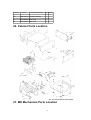
1
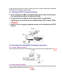
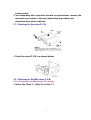
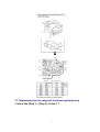
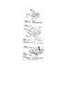
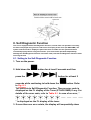
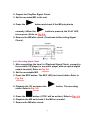
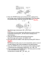
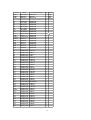
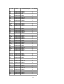
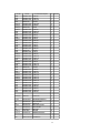
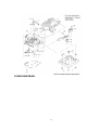
AD0003058C2
Mini Disc Deck
SJ-HD515
Mechanism Unit: MR3A
Colour
(S)..........Silver Type
Area
(E)..........Europe.
SPECIFICATIONS
1
2000 Matsushita Electric Industrial Co., Ltd. All rights reserved.
Unauthorized copying and distribution is a violation of law.
1. Note
Refer to the service manual for Model No. SE-HD515MD (ORDER No. AD0003056C2) for
information on Accessories and Packaging.
2. Blue LED
- The blue LED mounted to each sides of front panel is very
sensitive to static electricity. When handling the LED base plate,
be very careful about it.
- Do not replace the blue LED by itself because it may be subject to
electrostatic breakdown or deterioration in quality. When
replacing the LED base plate, be sure to replace L and R sides
simultaneously to adjust the brightness. For configuration at the
time of supply of replacement parts, refer to Printed Circuit Board
Diagram.
3. Before Repair
This equipment (SJ-HD515), which is a component of the system, is supplied with power from
the Amplifier (SE-HD515MD) through the Tuner (ST-HD515MD). When repairing this equipment
or checking operation of the system, be sure to connect to the amplifier and tuner with it.
This equipment, even in the state of it as a single equipment, permits power supply and
operation check. When operating it as a single equipment without the amplifier and tuner, refer
to the To Supply Power Source and Signal Check .
4. Handling Precautions for MD Unit
The laser diode in the MD unit (optical pickup) may break down due to potential difference
2
caused by static electricity of clothes or human body. So be careful of electrostatic breakdown
during repair of the MD unit (optical pickup).
4.1. Handling of MD Unit (optical pickup)
1. Do not subject the MD unit (optical pickup) to static electricity as
it is extremely sensitive to electrical shock.
2. To protect the breakdown of the laser diode, an anti-static
shorting pin is inserted into the flexible board (FPC board). Refer
to Fig. 4-1.
3. Take care not to apply excessive stress to the flexible board (FPC
board).
Fig. 4-1.
4.2. Grounding for electrostatic breakdown prevention
4.2.1. Human body grounding
Use the anti-static wrist strap to discharge the static electricity from your body. Refer to Fig. 4-2.
Fig. 4-2.
4.2.2. Work table grounding
Put a conductive material (sheet) or steel sheet on the area where the MD unit (optical pickup)
is placed, and ground the sheet. Refer to Fig. 4-3.
Fig. 4-3.
3
Caution:
The static electricity of your clothes will not be grounded through
the wrist strap.
So take care not to let your clothes touch the MD unit (optical
pickup).
5. Precaution of Laser Diode
6. Location of Controls
7. Operation Checks and Component Replacement /
Procedures
- This section describes procedures for checking the operation of
the major printed circuit boards and replacing the main
4
components.
- For reassembly after operation checks or replacement, reverse the
respective procedures. Special reassembly procedures are
described only when required.
7.1. Checking for the main P.C.B.
- Check the main P.C.B. as shown below.
7.2. Checking for the MD servo P.C.B.
7.2.1. Checking for the MD servo P.C.B. (A side)
- Follow the (Step 1) - (Step 3) of item 7.1.
5
- Check the MD servo P.C.B. (A side) as shown below.
7.2.2. Checking for the MD servo P.C.B. (B side)
6
7.3. Replacement for the magnetic head and optical pickup
- Follow the (Step 1) - (Step 3) of item 7.1.
7
8
9
10
7.4. Replacement for the belt and loading motor ass’y
- Follow the (Step 1) - (Step 3) of item 7.1.
11
12
7.5. Replacement for the traverse motor ass’y
- Follow the (Step 1) - (Step 3) of item 7.1.
- Follow the (Step 1) - (Step 11) of item 7.3.
13
14
8. Self-Diagnostic Function
This unit is equipped with a Self-Diagnostic Function, so that if the unit operates incorrectly,
the fault is displayed using an error code on the FL display of the Tuner (ST-HD515MD). The
system control IC and FL display are part of the tuner so make sure the system has been
connected properly before using this function. (This unit can be operated independently,
although the Self-Diagnostic Function cannot be used.) Use this Self-Diagnostic Function when
servicing the unit.
8.1. Setting to the Self-Diagnostic Function
1. Turn on the power.
2. Hold down the
button for at least 2 seconds and then
button for at least 2
press the
seconds while continuing to hold down the
button. Refer
to Fig. 8-1.
The unit sets to Self-Diagnostic Function. Then an error code is
displayed on the FL display of the Tuner (ST-HD515MD) if any. For
details of the error code, refer to Table 8-1. In case of no error, “
” is displayed on the FL display of the tuner.
3. If more than one error exists, the display will sequentially show
15
the respective error codes each time
button is pressed.
Fig. 8-1.
Table 8-1.
Error code
Symptom
F15
Interval till MD starts playing is
too long.
F28
MD cannot be loaded.
Possible cause
-Traverse det. switch (S8) is defective; Check and replace if necessary.
-Confirm that the disc is not catching on anything.
-The connection (flexible circuit board or connector cable) betweenthe
and MD servo circuit board is disconnected or damaged; check and replace
necessary.
F29
-The MD unit may be malfunctioning; replace it.
-Confirm that the disc is not catching on anything.
-The connection (flexible circuit board or connector cable) betweenthe
MD cannot be ejected.
and MD servo circuit board is disconnected or damaged; check and replace
necessary.
-The MD unit may be malfunctioning; replace it.
8.2. Canceling the Self-Diagnostic Function
The Self-Diagnostic Function can be canceled by pressing the power button (POWER) on the
Amplifier (SE-HD515MD) to turn off the system. And then pressing the power button again to
turn it on again.
8.3. Clearing the Self-Diagnostic Function
The contents of abnormality display are stored in memory. In order to clear the memory,
continue to press the STOP button for at least 2 seconds while in the Self-Diagnostic Function.
The memory will clear. Always be sure to clear this memory after completing repair.
9. To Supply Power Source and Signal Check
Caution:
- It is very dangerous to look at or touch the laser beam. (Laser
radiation is invisible.) With the unit turned ON, laser radiation is
16
emitted from the pickup lens.
- Avoid exposure to the laser beam, especially when performing
adjustments.
This unit (SJ-HD515) is designed to operate on power supplied
from the Amplifier (SE-HD515MD) through the Tuner (STHD515MD). When connecting the unit to other system components,
do not connect to the Amplifier (SE-HD515MD) directly. When
operating the unit (SJ-HD515) alone for testing and servicing
without having power supplied from the Amplifier (SE-HD515MD),
use the following method.
9.1. Power Supply to This Unit alone
1. Setting of the unit switches: Set MARKING to AUTO and TRACK
to ONE. Refer to Fig. 9-1.
2. Short the IC10-pin 67 (TP77) and GND (TP74) with the lead wire.
Refer to Fig. 9-2. (This enables the unit to enter the operation
mode and to active the operation switches on the front panel.)
3. Apply DC 10 V between the CP304-pin 5 (+10 V) and CP304-pin 11
(GND). Refer to Fig. 9-3. (The LED of REC and PLAY will light up.
The PLAY LED is orange color.)
Fig. 9-1.
Fig. 9-2.
17
Fig. 9-3.
9.2. Preparation for Play/Rec Signal Check
Connect the oscilloscope or the speaker with built-in amplifier to the section between CP304pin 12 (R ch OUT) and CP304-pin 17 (A.GND) as well as the section between CP304-pin 14 (L ch
OUT) and CP304-pin 17 (A.GND) and check if the signals are outputting from this unit. Refer to
Fig. 9-3.
9.3. Checking Play/Rec Signal to This Unit alone
9.3.1. Necessary Instruments
- Recorded MD
- Recordable MD
- Optical fiber cable
- Portable CD player and CD
(You can check this operation with any other player that has an
optical digital output terminal but the portable CD player. The
following procedure explains check operation with the portable
CD player, but the procedure is the same for other players.)
9.3.2. Playback Signal Check
1. Set the unit so that Power Supply to This Unit alone as previously
explained.
18
2. Prepare for Play/Rec Signal Check.
3. Set the recorded MD in the unit.
4. Press the
button and check if the MD play backs
normally. (When the
button is pressed, the PLAY LED
turns green.) Refer to Fig. 9-4.
5. Remove the MD after check. (Continued to Recording Signal
Check.)
Fig. 9-4.
9.3.3. Recording Signal Check
1. After completing the item 5 of Playback Signal Check, connect to
the portable CD player (or any other player with an optical digital
output terminal). Refer to Fig. 9-5.
2. Set the recordable MD.
3. Press the REC button. The REC LED (red color) blinks. Refer to
Fig. 9-4.
4. Playback the CD and press the
starts. Refer to Fig. 9-4.
5. Press the
button. The recording
button. (UTOC will be written.) Refer to Fig. 9-4.
6. Playback the MD and check if the MD is recorded.
7. Remove the MD after check.
19
8. Turn off the power, and remove the lead wire between the IC10pin 67 (TP77) and GND (TP74). (Refer to Power Supply to This Unit
alone.)
Fig. 9-5.
10. Schematic Diagram Notes
- This schematic diagram may be modified at any time with the
development of new technology.
Notes:
S1:
PROTECT det. switch
S2:
REFLECT det. switch
S3:
LOAD OPEN det. switch
S4:
DISC IN det. switch
S5:
LOAD PLAY/REC det. switch
S6:
LOAD PLAY det. switch
S7:
LOAD TRG det. switch
S8:
20
Traverse det. switch
S401:
Eject switch (
EJECT)
S402:
CD edit recording switch (CD EDIT)
S403:
Enter switch (ENTER)
S404:
Edit switch (EDIT)
S405:
Stop switch (
)
S406:
Pause switch (
)
S407:
Playback switch (
)
S408:
Record switch (REC)
S409:
R.Skip/search switch (
)
S410:
F.Skip/search switch (
)
S411:
Marking mode select switch in AUTO position (MARKING)
21
S412:
One track/all tracks switch in ONE position (TRACK)
VR1:
Laser power adjustment VR
- Indicated voltage values are the standard values for the unit
measured by the DC electronic circuit tester (high-impedance)
with the chassis taken as standard. Therefore, there may exist
some errors in the voltage values, depending on the internal
impedance of the DC circuit tester.
No mark
: MD Stop
()
: MD Play
<>
: MD Rec
- Important safety notice:
Components identified by mark have special characteristics
important for safety.
Furthermore, special parts which have purposes of fire-retardant
(resistors), high-quality sound (capacitors), low-noise (resistors),
etc. are used.
When replacing any of components, be sure to use only
manufacturer’s specified parts shown in the parts list.
- Caution!
IC and LSI are sensitive to static electricity.
Secondary trouble can be prevented by taking care during repair.
Cover the parts boxes made of plastics with aluminum foil.
Ground the soldering iron.
Put a conductive mat on the work table.
Do not touch the legs of IC or LSI with the fingers directly.
- Voltage and signal line
: Positive voltage line
22
: Playback signal line
: Recording signal line
11. Schematic Diagram
12. Printed Circuit Board Diagram
13. Type Illustration of ICs, Transistors and Diodes
14. Wiring Connection Diagram
15. Block Diagram
16. Troubleshooting Guide
17. Terminal Function of ICs
17.1. IC1 (AN8772FHQ): RF Amp
23
Function
Pin Terminal I/O
No. Name
1 CENVD
I D signal detection input
2
LDO
O LD amp output terminal
3 APC PD
I Photo diode detection input
4 LD IN
I LD amp input
5
APC
I APC amp reference voltage
REF
input
6 TEMP IN I Temperature sensor amp input
7 TEMP
O Temperature sensor amp output
8
ADIP
O ADIP FM signal output
9 TOFS
I Tracking error off-set
adjustment input
10 TBAL
I Tracking balance adjustment
signal input
11
TE
O Tracking error signal output
12 CRS IN
I Track cross signal input
13 TGAIN
I TE gain adjustment input
14
LNP
O Lens position signal output
15 AB GAIN I APP signal gain adjustment
input
16
FE
O Focus error signal output
17 AS GAIN I AS gain adjustment input
18 FBAL
I Focus balance adjustment input
19
AS/
O AS signal output
MON3T
20 CEA
I 3T envelope detection input
21 BDO/
O BDO/Track cross signal output
TRCRS
22 CBD O
O BDO detection capacitor
terminal
23 OFT O
O Off-track detection signal output
24 GND
- GND terminal
25 OFT IN
I Off-track detection signal input
26
I Power supply terminal
VCC
27 NRFDET
/ OFTR
28 NRFLD
O
31 NRFSTBY
I
RF detect signal output/Offtrack signal output
Serial command latch signal
input
Serial command data signal
input
Serial command clock signal
input
Standby control signal input
29
I
32 OUT RF
O
EFM signal output
30
RF
DATA
RFCK
I
I
24
Pin Terminal
No. Name
33 CRF
AGC
34 EQ IN
35 ARFO
36 SVREF
37 VREF
38
RF1
39
RF2
40
F1
41
F2
42 CLPF1
I/O
43 CLPF1
I
44
A
45
B
46
C
47
D
48 CENVC
I
I
I
I
I
I
O
I
O
I
I
I
I
I
Function
RFAGC capacitor connect
terminal
EQ input
RF amp output
Reference signal input
Reference voltage output
RF 1 signal input
RF 2 signal input
F 1 signal input
F 2 signal input
APP correction CPF capacitor
connect terminal
RF equalizer adjustment
resistor connect terminal
Main beam A signal input
Main beam B signal input
Main beam C signal input
Main beam D signal input
C signal detection input
17.2. IC2 (AN8814SB-E1): / Focus/Tracking Coil, / Spindle/Traverse
Motor Drive
Pin Terminal
No. Name
1 REG B
I/O
Function
-
3.3 V external transistor control
(Not used, open)
3.3 V regular output monitor
(Not used, connected to GND)
Not used, open
Op-amp output
Op-amp invert input
2
REG M
-
3
4
5
6
NC
OPO
OPOP+
O
I
-
7
VCC
I
Op-amp non-invert output
(Not used, connected to GND)
Power supply terminal
8 1/2PVCC
2
O
9
I
1/2PVCC output terminal 2
(Connected to GND via
capacitor)
Power supply terminal for driver
O
O
O
GND terminal
Tracking coil drive output
Tracking coil drive output
Focus coil drive output
10
11
12
13
PVCC2
PGND2
VO4VO4+
VO3-
25
Pin Terminal
No. Name
14 VO3+
15 VO216 VO2+
17 VO118 VO1+
19 PGND1
20 PVCC1
I/O
Function
O
O
O
O
O
I
Focus coil drive output
Traverse motor drive output
Traverse motor drive output
Spindle motor drive output
Spindle motor drive output
GND terminal
Power supply terminal
21 1/2PVCC
1
O
22
23
24
25
VREF
IN1
PC1
IN2
I
I
I
I
26
27
26
PC2
IN3
IN4
I
I
I
1/2PVCC output terminal 1
(Connected to GND via
capacitor)
Reference voltage input
Spindle motor drive signal input
Power cut 1 input
Traverse motor drive signal
input
Power cut 2 input
Focus drive signal input
Tracking drive signal input
17.3. IC3 (MN66616RA4): / ATRAC Encoder/Decoder, Servo Signal
Processor
Function
Pin Terminal I/O
No. Name
1 ADIP
I ADIP FM signal input
2
LNP
I Lens position signal input
3
FE
I Focus error signal input
4
TE
I Tracking error signal input
5
AS
I AS signal input
6 DRMONI I Drive voltage monitor input
7
BAT
8 AMONI
I
-
9 VREFI
10 TOFS
I
O
11
FBAL
O
12
TBAL
O
13 TGAIN
O
Battery power supply terminal
Servo analog monitor signal
output
(Not used, open)
Reference voltage input
Tracking error off-set
adjustment output
Focus balance adjustment
output
Tracking balance adjustment
output
TE error gain adjustment output
26
Function
Pin Terminal I/O
No. Name
14 ASGAIN O Main beam amp gain
adjustment output
15 ABGAIN O APP adjustment output
16 AVDD1
I Power supply terminal
17 AVSS1
18 FOD
19 TRD
20 TVD
-
GND terminal
O
O
O
21
O
Focus drive signal output
Tracking drive signal output
Traverse motor drive signal
output
Spindle motor drive signal
output
Drive IC spindle ON signal
output
Drive IC traverse ON signal
output
Power supply terminal
SPD
22 SPON
O
23 TVON
O
24 DVDD0
25
FG
26 NRECT
27 IVDD2
I
I
O
I
28
IVDD0
-
29 DVSS0
-
30 RAD12
|
| RAD10
32
33 RAD9
|
|
RAD0
42
43 RDT3
|
|
RDT0
46
47 NRAS
FG input
Rec/Play switching signal output
Power supply terminal for I/O
pad
Power supply terminal for I/O
pad
GND terminal
-
DRAM address output (Not
used, open)
O
DRAM address output
I/O
DRAM data input/output
O
48 NCAS
O
49 NWE
50 NRST
51 SELAD
O
I
I
52 SSCK
I
DRAM row address strobe
signal output
DRAM column address strobe
signal output
DRAM write enable signal output
Reset signal input
MSP/MDA, I/F address select
signal input
MSP/MDA, I/F clock signal input
27
Function
Pin Terminal I/O
No. Name
53 SSDW
I MSP/MDA, I/F write data input
54 SSDR
O MSP/MDA, I/F read data output
55 MDISY
O Leader synchronous signal
output
56 SCTSY O ADIP synchronous noise output
57 SGSYNC O Frame synchronous signal
output
58 DVDD1
I Power supply terminal
59
IVDD1
I
60 DVSS1
61 FS384
62 SCL
63 SWS
64 SDAP
65 SDAR
66 LRCK
67 BCK
68 DATA
69
TX
O
O
O
O
I
I
I
I
-
70
RX1
I
71
RX2
I
72 NREFM
-
73 REFM
74 MONI3
O
-
75 MONI2
-
76 MONI1
-
77 MONI0
-
78
TS3
-
79
TS2
-
80
TS1
-
Power supply terminal for I/O
pad
GND terminal
384 Fs output
Bit clock signal output
Word clock signal output
Audio data signal output
Audio data signal input
CD word clock signal input
CD bit clock signal input
CD data signal input
Digital audio interface signal
output
(Not used, open)
Digital audio interface signal 1
input
Digital audio interface signal 2
input
EFM modulation inverted output
(Not used, open)
EFM modulation signal output
Monitor signal output (Not
used, open)
Monitor signal output (Not
used, open)
Monitor signal output (Not
used, open)
Monitor signal output (Not
used, open)
Reserved (Not used, connected
to GND)
Reserved (Not used, connected
to GND)
Reserved (Not used, connected
to GND)
28
Function
Pin Terminal I/O
No. Name
81 TS0
- Reserved (Not used, connected
to GND)
82EXSYSCK - External system clock input
I
(Not used, connected to GND)
Power supply terminal
83 DVDD2
84
XI
85
XO
86 VDSS2
I
O
-
Crystal oscillator (f=16.9344
MHz)
87 RFDAT
88 RFCK
89 NRFLD
90 TRCRS
91 OFTR
92 APCD
93EXEFMCK
O
O
O
I
I
O
I
RF serial data output
RF serial clock output
RF serial load output
Track cross signal input
Off-track signal input
Laser power PWM output
GND terminal
94 PEFM1 O
95 EEMIREF I
External FM clock input
(Connected to GND via resistor)
EFM loop filter output
EFM PLL reference current input
96EEMPLLF O
EFM signal output
97 PEFMS
98 AVDD0
99 AVSS0
I
I
EFM signal input
Power supply terminal
-
GND terminal
100 TEFSEL
-
Not used, open
17.4. IC10 (MN101D03DAA1): / System Control
29
Pin Terminal
No. Name
1
DAC
RST
2
DEO
3
MUTE
I/O
Function
O
DAC reset signal output (L:
reset)
O
O
O
DE emphasis signal output
(L: DE emphasis)
Muting signal output (Not used,
open)
AD reset signal output (L: reset)
RF amp standby control signal
output
Power supply control output
Reset signal output
-
4 AD RST
5
NRF
STBY
6
PC
7
MSP
RST
8 LOAD1
9 LOAD0
10 NEFMON
O
O
O
O
O
Loading motor drive 1 output
Loading motor drive 0 output
Magnetic head current output
11 TEST01
-
12 TV SW
13 DISC IN
I
I
14 REFLECT
I
15LOADSW0
/
(OPEN)
16LOADSW1
I
Test terminal (Not used, open)
Rest detect switch signal input
Disc in detect switch signal
input
Reflect detect switch signal
input
Load OPEN detect switch signal
input
I
Load TRG detect switch signal
input
I
Load PLAY/REC detect switch
signal input
I
Load PLAY detect switch signal
input
19 PROTECT
I
20 MMOD
21
RST
22 UNITTEST
I
-
23
-
Write protect tab detect switch
signal input
Not used, connected to GND
Reset signal input
Test signal input (Not used,
open)
Test signal input (Not used,
open)
ADIP synchronous noise input
Header synchronous noise input
Panel I/F request signal input
/ (TRG)
17LOADSW2(
/ PLAY/
REC)
18LOADSW3
/
(PLAY)
CS2
24 SCTSY
25 MDISY
26 PANEL
/ REQ
I
I
I
30
/ REQ
Pin Terminal
No. Name
27 LED
OUT1
28 LED
OUT2
29 LED
OUT3
30 TEST02
31
32
33
34
VDD
2(3V)
OSC1
OSC2
I/O
Function
O
Drive signal output for LED
drive (H: ON)
-
Test terminal (Not used, open)
Power supply terminal
I
I
O
-
Crystal oscillator (f=10.02 MHz)
-
Not used, connected to GND
Not used, open
GND terminal
-
Test terminal (Not used, open)
39 EEPCS
-
EEPROM chip select signal
output
(Not used, open)
40 EEPCK
-
EEPROM clock signal output
(Not used, open)
41 EEPDATA
-
EEPROM data signal input/
output
(Not used, connected to GND
via resistor)
42 TEST04
-
Test terminal (Not used, open)
43 TEST05
-
44
I
Test terminal (Not used, open)
MDA synchronous signal input
35
36
37
VSS
XI
XO
VSS
38 TEST03
GND terminal
CF
SYNC
45 TEST06
-
46 TEST07
I
47 TOK OK
-
48 HF ON
49 PANEL
CLK
50 PANEL
DATA I
51 PANEL
DATA O
52 PANEL
CS
O
I
Test terminal (Not used, open)
HF module ON signal output
PANEL I/F clock signal input
I
PANEL I/F data signal input
O
PANEL I/F data signal output
O
PANEL I/F chip select signal
output
Test terminal (Not used, open)
Connected to rec/play switch
signal
31
Pin Terminal
No. Name
53 SELAD
54
55
56
57
I/O
O
Function
MSP/MDA, I/F address select
output
(H: address)
MSP/MDA, I/F clock output
MSP/MDA, I/F read data input
MSP/MDA, I/F write data output
SS CLK
SS DR
SS DW
LCD CK
O
I
O
-
58 ADRS /
TEST
RXD
-
Test terminal
(Connected to power supply via
resistor)
59
LCD
DATA /
TXD
VREFTEMP
KEY1
KEY2
MO
LOAD
SRV
TEST
LOAD P
-
Test terminal (Not used, open)
I
I
I
-
TEST
KEY / IN
68 SRV
LOAD
69 VCC3V
-
Connected to GND
Temperature sensor input
Operation key signal input
Operation key signal input
Test signal input (Not used,
open)
Test signal input (Not used,
open)
Test signal input (Not used,
open)
Test signal input (Not used,
open)
I
Test signal input (Not used,
open)
Power supply terminal
70 VCC5V
71 SEL
ADDA
I
Power supply terminal
-
72 SLOCK
-
73 TLOCK
-
AD/DA converter select signal
input
(Not used, open)
Spindle lock output (Not used,
open)
Tracking lock output (Not used,
open)
74 FLOCK
-
Focus lock test signal output
(Not used, open)
75 ERROR
-
Servo error test signal output
(Not used, open)
76
-
Servo busy test signal output
(Not used, open)
60
61
62
63
64
65
66
67
BUSY
-
-
LCD clock test signal output
(Connected to power supply via
resistor)
32
Pin Terminal
No. Name
77 SBP /
RETRY
78 SRV /
RETRY
I/O
Function
-
Spindle management retry test
signal output (Not used, open)
-
Servo retry test signal output
(Not used, open)
79 ARDSKIP
-
Address skip test signal output
(Not used, open)
80 SPMWE
-
SPM test signal output
(Not used, open)
17.5. IC72 (M51V4400D7FS): / 4M DRAM
Pin Terminal
No. Name
1
DO1
2
DO2
3
WE
4
RAS
5
A9
9
A0
10
|
12
13
14
|
18
22
I/O
I/O
I/O
I
I
I
I
Function
DRAM
DRAM
DRAM
DRAM
DRAM
DRAM
data 1 input/output
data 2 input/output
write enable input
row address strobe input
address 9 input
address 0 input
A1
|
A3
I
DRAM address 1 - 3 input
VCC
I
Power supply terminal
A4
|
A8
I
DRAM address 4 - 8 input
OE
-
23
CAS
24
25
26
DO3
DO4
VSS
DRAM output enable input
(Not used, connected to GND)
I DRAM column address strobe
input
I/O DRAM data 3 input/output
I/O DRAM data 4 input/output
- GND terminal
18. Measurements and Adjustments
Note:
Because this unit uses the optical magnetic recording, the unit
outputs over 10 times more laser than a CD player does. In
adjustment mode, the laser is always being output. Therefore, be
33
especially careful not to look laser beam directly or to touch the
laser beam when adjusting the unit and checking its operation.
18.1. Laser Power Adjustment
Adjust each laser power: read power for reading (play) and write power for writing (record).
18.1.1. Necessary Instruments
- Laser power meter (LE8010)
- Test disc (Pre-mastered disc RFKV0006 or RFKV0014)
- Recordable disc available on sales route (with music recorded)
- Insulated driver for adjustment such as a ceramic driver
18.1.2. Set the Unit to the Adjustment Mode
Perform the (Step 1) and (Step 2) in the item 7.2. Checking for the MD servo P.C.B. in Operation
Checks and Component Replacement Procedures.
Caution:
1. About handling the MD unit
- The magnetic head is precision unit and is very fragile. Do not
deform it.
- Laser diode in the optical pickup may be destroyed by the
static electricity generated in your clothes or body. Be
especially careful with the static electricity.
- The optical pickup is structured extremely precisely. Do not
subject to the strong impact or shock. Do not touch the lens.
2. About handling the magnetic head
When replacing the magnetic head, do not tighten the mounting
screw (RHD17022) too firmly. If the screw is tightened too much
to deform the resin, the position of the head is moved, and this
affects its recording operation.
Recommended torque for mounting screw: / 700±100 g cm
Reference:
This is the same force as using a screwdriver with a 15-mm
diameter grip, you fasten the screw naturally with your thumb and
index finger.
3. About the driver for adjusting laser power
Use only insulated driver such as a ceramic driver. With the metal
driver, it is not possible to adjust properly because of induction
noise. Also, if it short-circuits with the chassis, it may destroy or
34
damage the laser diode.
Recommended driver: VESSEL 9000 1.8-30 / (Ceramic driver)
Caution on optical pickup:
- The optical pickup and the magnetic head are structured precisely;
therefore, they are very fragile. Be careful not to touch them with
the edge of laser power meter.
- The sensor of the laser power meter is a very fine part. Be careful
not to touch it to the optical pickup lens.
- The focus point of the laser reaches to 180°C. Therefore, avoid
using laser power for a long time because the sensor of the laser
power meter may be burned.
- Do not allow the write power to even momentarily reach or exceed
5.5 mW. Doing so will result in damage to the optical pickup.
- Do not set the unit to the laser power adjustment mode with the
MD loaded. Doing so may result in damage to the MD.
18.1.3. Adjustment Procedure
1. Remove the MD unit from the system unit.
2. Short-circuit the IC10-pin 67 (TP77) and GND (TP74) with the lead
wire. (This enables the unit to enter the operation mode and to
active the operation switches on the front panel.)
3. Set the MD unit in the system unit and turn on the power. The LED
of REC and PLAY will light up.
4. Slide the sensor cover of the laser power meter. / Refer to Fig. 181.
Fig. 18-1.
5. Position the sensor of the laser power meter directly above the
optical pickup. Refer to Fig. 18-2.
Fig. 18-2.
35
6. Press the CD EDIT button and confirm that the reading of the
laser power meter is within the specified range. If it is not within
the specified range, adjust by turning VR1. Refer to Fig. 18-3.
Fig. 18-3.
Specified range (read power): 600
W or lower
Caution:
Proceeding on to the subsequent adjustment procedure with the
read power exceeding 600
W will result in damage to the
optical pickup.
7. Press the CD EDIT button and read the write power.
Specified range (write power): 4.8 mW±0.1 mW
8. If it is not within 4.8 mW±0.1 mW, adjust by turning VR1. Refer to
Fig. 18-3.
Caution:
Do not allow the write power to even momentarily reach or exceed
5.5 mW. Doing so will result in damage to the optical pickup.
9. Press the CD EDIT button, the read power will be displayed again.
/ Confirm that the read power is within 540
W ~ 660 W.
10. Then, again press the CD EDIT button. The laser power recorded
in the laser ROM will be displayed.
Confirm that it is within 540 W ~ 660 W.
36
11. Press the STOP button and exit the adjustment mode.
12. Turn off the power and remove the lead wire between the IC10pin 67 (TP77) and GND (TP74). This ends the adjustment mode.
19. Replacement Parts List
Notes:
- Important safety notice:
Components identified by mark have special characteristics
important for safety.
Furthermore, special parts which have purposes of fire-retardant
(resistors), high-quality sound (capacitors), low-noise (resistors),
etc. are used.
When replacing any of components, be sure to use only
manufacture’s specified parts shown in the parts list.
- The marking [RTL] indicates that Retention Time is Limited for this
item. After the discontinuation of this assembly in production, the
item will continue to be available for a specific period of time. The
retention period of availability is dependent on the type of
assembly, and in accordance with the laws governing part and
product retention. After the end of this period, the assembly will
no longer be available.
- All parts are supplied by MESA.
37
Ref. No.
Part No.
Part Name & Description
Pcs Remarks
1
RHD30007-S
SCREW
4
2
RKM0364-2S1
CABINET
1
3
RYQ0274-S
SIDE PANEL UNIT(L)
1
3-1
XTBS26+8J
SCREW
1
4
RKA0114-K
FOOT
4
4-1
RKA0083-K
CUSHION
4
5
RGG0148B-S
FRONT PANEL
1
6
RYQ0275-S
SIDE PANEL UNIT(R)
1
6-1
XTBS26+8J
SCREW
1
7
REP2683F-S
LED PCB
1
8
XTBS3+10JFZ1
SCREW
1
9
RGK0977-2S
MD LID
1
10
RGL0386-Q
LENS1
1
11
RGL0387-Q
LENS2
1
12
RGP0642-1S
SUB PANEL
1
13
RGU1599A-1S
BUTTON,OPERATION
1
14
RHD20010
SCREW
1
15
RMB0514
SPRING
1
16
XTBS26+8J
SCREW
4
17
XTBS3+8JFZ1
SCREW
12
18
XTB3+5JFZ
SCREW
4
19
REZ1048
FFC(30P)
1
100
RED0047-1
MAGNETIC HEAD
1
101
RHD17021
SCREW
1
102
RHD17022
SCREW
1
103
RMC0348
SPRING
1
104
RMC0349
NUT PLATE SPRING
1
105
RML0515
HEAD SIFTER
1
106
RMQ0750
REF BASE
1
107
RMQ0751
NUT PLATE
1
108
RMS0611
MAIN SHAFT
1
109
RXJ0021
DRIVE SHAFT
1
110
RXK0249
MECHANISM CHASSIS
1
110-1
RDV0055
BELT
1
110-2
REM0077
TRAVERSE MOTOR
1
110-3
REM0078
LOADING MOTOR
1
110-4
RMB0548
SPRING
1
110-5
RMQ0752
DETECTOR PIN 1
1
110-6
RMQ0753
DETECTOR PIN 2
2
110-7
XQN17+C25FZ
SCREW
4
110-8
XYC2+FF105
SCREW
1
111
RAF1700A
OPTICAL PICK-UP
1
112
XTW2+6S
SCREW
1
113
RHD20053
SCREW
4
114
RMB0504
SPRING
4
115
RMG0447-K
DUMPER
4
116
XTN17+6GFZ
SCREW
1
117
RXQ0558
HOLDER
1
C1
ECUV1H221KBV 50V 220U
1
C4
ECUVNA105ZFV 10V 1U
1
C5
ECUVNA224KBV 10V 0.22U
1
C6
ECUVNA105ZFV 10V 1U
1
38
Ref. No.
Part No.
Part Name & Description
Pcs Remarks
C7,C8
ECUVNA224KBV 10V 0.22U
2
C11
ECUVNE223KBV 25V 0.022U
1
C12
ECUV0J474KBV 6.3V 0.47U
1
C13
ECUV1C393KBV 16V 0.039U
1
C14
ECUV1H102KBV 50V 1000P
1
C15
ECST0GY106RR 4V 10U
1
C16
ECUV1H181KV
1
C17
ECUV1H332KBV 50V 3300P
1
C18
ECUV1H562KBV 50V 5600P
1
C19
ECUVNC104ZFV 16V 0.1U
1
C20
ECST0GY106RR 4V 10U
1
C21
ECUV1H822KBV 50V 8200P
1
C22
ECUV1H102KBV 50V 1000P
1
C23
ECUVNC104ZFV 16V 0.1U
1
C24
ECUV1H102KBV 50V 1000P
1
C25
ECUV1C393KBV 16V 0.039U
1
C26
ECUV1H472KBV 16V 4700P
1
C28
ECST0GY226RR 4V 22U
1
C29
ECUV1H332KBV 50V 3300P
1
C30
ECUV1E123KBV 25V 0.012U
1
C31,32
ECUV1H102KBV 50V 1000P
2
C33
ECST0GY106RR 4V 10U
1
C34,35
ECUV1H102KBV 50V 1000P
2
C37
ECUV1H181KV
50V 180P
1
C40
ECUVNC104ZFV 16V 0.1U
1
C41
ECEV0JA331P
1
C42
ECST0GY106RR 4V 10U
1
C45
ECST0GY106RR 4V 10U
1
C46
ECUVNC104ZFV 16V 0.1U
1
C47
ECUVNA105ZFV 10V 1U
1
C48
ECUVNC104ZFV 16V 0.1U
1
C50
ECUVNC104ZFV 16V 0.1U
1
C51,52
ECUVNA105ZFV 10V 1U
2
C53
ECUV1H332KBV 50V 3300P
1
C55-58
ECUV1H102KBV 50V 1000P
4
C59
ECUV1C823KBV 16V 0.082U
1
C60
ECEV1CA100NR 16V 10U
1
C61
ECUV0J334KBV 16V 0.33U
1
C62
ECUV1H221KBV 50V 220P
1
C64
ECUVNE153KBV 25V 0.015U
1
C65
ECUVNC104KBV 16V 0.1U
1
C66
ECUV1C823KBV 16V 0.082U
1
C67
ECUV1H392KBV 50V 3900P
1
C70
ECUV1E123KBV 25V 0.012U
1
C71-76
ECUVNC104ZFV 16V 0.1U
6
C79,80
ECUVNC104ZFV 16V 0.1U
2
C81
ECUV1H560JCV 50V 56P
1
C82
ECUVNC473KBV 16V 0.047U
1
C83,84
ECUVNC104ZFV 16V 0.1U
2
C85
ECST0GY106RR 4V 10U
1
C86
ECUVNE153KBV 25V 0.015U
1
C87
ECUVNC104ZFV 16V 0.1U
1
C88,89
ECUV1H331KBV 50V 330P
2
C90,91
ECUV1H080DCV 50V 8P
2
50V 180P
6.3V 330U
39
Ref. No.
Part No.
Part Name & Description
Pcs Remarks
C92,93
ECUVNC104ZFV 16V 0.1U
2
C94
ECST0GY475RR 4V 4.7U
1
C95
ECUVNC104ZFV 16V 0.1U
1
C96,97
ECST0GY475RR 4V 4.7U
2
C98
ECUVNC104ZFV 16V 0.1U
1
C99
ECUV1H102KBV 50V 1000P
1
C100
ECUVNC104ZFV 16V 0.1U
1
C101
ECST0GY106RR 4V 10U
1
C102
ECUVNC104ZFV 16V 0.1U
1
C103
ECST0GY106RR 4V 10U
1
C106
ECUV1H102KBV 50V 1000P
1
C110
ECUVNC104ZFV 16V 0.1U
1
C111
ECST0GY106RR 4V 10U
1
C112
ECEV1CA100NR 16V 10U
1
C113
ECUVNC104ZFV 16V 0.1U
1
C114,15
ECUV1H561KBV 50V 560P
2
C117
ECEV0JA331P
1
C118
ECUVNA105KBN 10V 1U
1
C119
ECUV1H102KBV 50V 1000P
1
C120
ECUV1H560JCV 50V 56P
1
C121
ECUV1H102KBV 50V 1000P
1
C122
ECUVNA105ZFV 10V 1U
1
C123
ECUVNC104ZFV 16V 0.1U
1
C128
ECUVNC104ZFV 16V 0.1U
1
C129
ECUV1H101JCV 50V 100P
1
C133
ECUVNA105ZFV 10V 1U
1
C134
ECUV1H331KBV 50V 330P
1
C138
ECEV0JA470SR 6.3V 47U
1
C139-42
ECUVNC104ZFV 16V 0.1U
4
C143
ECST0GY106RR 4V 10U
1
C144
ECUVNH103KBV 50V 0.01U
1
C147-49
ECUVNH103KBV 50V 0.01U
3
C154,55
ECUV1H330GCV 50V 33P
2
C311,12
RCE1CKA470BG 16V 47U
2
C314,15
ECUV1H222KBN 50V 2200P
2
C317
ECUVNE104ZFN 25V 0.1U
1
C318
ECEA0JKS101
1
C319
ECUVNE104ZFN 25V 0.1U
1
C320
ECEA0JKS101
1
C321
ECUVNE104ZFN 25V 0.1U
1
C322
ECEA0JKS101
1
C323,24
ECUVNE104ZFN 25V 0.1U
2
C325
ECA1CM222
1
C327-29
ECUVNE104ZFN 25V 0.1U
3
C331
ECUVNE104ZFN 25V 0.1U
1
C351,52
ECEA1CKS220
16V 22U
2
C353
ECUVNE104ZFN 25V 0.1U
1
C355
ECEA1AKS221
1
C356
ECUV1H101JCN 50V 100P
1
C357,58
ECUVNE104ZFN 25V 0.1U
2
C361-64
ECUVNE104ZFN 25V 0.1U
4
C365
ECUVNC105ZFN 16V 1U
1
C366
ECEA0JKS101
6.3V 100U
1
C401,02
ECUV1H103KBN 50V 0.01U
2
6.3V 330U
6.3V 100U
6.3V 100U
6.3V 100U
16V 2200U
6.3V 220U
40
Ref. No.
Part No.
Part Name & Description
Pcs Remarks
CN1
RJS2A4526T
CONNECTOR(26P)
1
CN4
RJS2A4830T
CONNECTOR(30P)
1
CN6
RJU113W10M
CONNECTOR(10P)
1
CN8
RJS2A4506T
CONNECTOR(6P)
1
CP6
RJT113W10M
CONNECTOR(10P)
1
CP302
RJS10T6ZA
CONNECTOR(10P)
1
CP303
RJS2A3330
CONNECTOR(30P)
1
CP304
RJT065A19
SYSTEM CONNECTOR(19P)
1
D5,D6
SC80209TE12R
DIODE
2
D9
MA728TX
DIODE
1
D301
MA4033M
DIODE
1
D302,03
MA719TA
DIODE
2
D401
SML79420C
LED
1
D402
LNJ201LPQJA
LED
1
IC1
AN8772FHQ
IC
1
IC2
AN8814SB-E1
IC
1
IC3
MN66616RA4
IC
1
IC4
AK4518VF-E2
IC
1
IC5
RN5RG33AA-TL IC
1
IC6
TC7W04FTE12L IC
1
IC9
RN5RZ26BA-TR IC
1
IC10
MN101D03DAA1 IC
1
IC11
TC74HCT00AFL IC
1
IC72
M51V4400D7FS
IC
1
IC92
LB1830MS-TLM
IC
1
IC301
PST597ENR
IC
1
IC303
TC74HCT7007A
IC
1
IC304
M5M34051FPE1 IC
1
IC306
BA17805T
IC
1
IC307
BA178M05T
IC
1
IC308
BA17805T
IC
1
IC309
S81233SGY-Z
IC
1
ICP301
SRUN20T
IC PROTECTOR
1
L1
RLQU100KT-W
COIL
1
L2,L3
RLQU101KT-W
COIL
2
L4-L8
RLQU2R2MT-W
COIL
5
L9-12
RLQU100KT-W
COIL
4
L13,14
RLQU2R2MT-W
COIL
2
L15
RLQU100KT-W
COIL
1
L16
RLQU2R2MT-W
COIL
1
L17,18
RLQP1R8KT2-Y COIL
2
L301
RLQZB470KT-D COIL
1
L303-05
RLQZP1R0KT-Y COIL
3
L307-10
RLQZP1R0KT-Y COIL
4
PCB1
REP2775AA-S
MAIN P.C.B.
1
PCB2
REP2683F-S
LED P.C.B.(REF.No.7)
1
41
[RTL]
Ref. No.
Part No.
Part Name & Description
Pcs Remarks
PCB3
REP2775AB-S
PANEL P.C.B
1
[RTL]
PCB4
REP2575A
SW P.C.B.
1
[RTL]
PCB5
REP2761A-T
SERVO P.C.B.
1
[RTL]
Q1
2SB1295-6-TB
TRANSISTOR
1
Q2
DTC114YETL
TRANSISTOR
1
Q3
2SB1462STX
TRANSISTOR
1
Q5
2SB1295-6-TB
TRANSISTOR
1
Q6
DTC114YETL
TRANSISTOR
1
Q10
2SJ278MYTR
TRANSISTOR
1
Q11
2SK1764KYTR
TRANSISTOR
1
Q13
2SB1121ST-TD
TRANSISTOR
1
Q301
UN5214TX
TRANSISTOR
1
Q302,03
DTA114YUA106 TRANSISTOR
2
Q304,05
UN5214TX
TRANSISTOR
2
Q306
2SB709ATX
TRANSISTOR
1
Q307
UN5214TX
TRANSISTOR
1
Q308
UN5111TX
TRANSISTOR
1
Q309
UN5214TX
TRANSISTOR
1
Q315
2SB709ATX
TRANSISTOR
1
R1
ERJ3GEYJ472V 1/16W 4.7K
1
R2
ERJ3GEYJ102V 1/16W 1K
1
R3
ERJ3GEYJ472V 1/16W 4.7K
1
R5
ERJ3GEYJ1R0V 1/16W 1
1
R6
ERJ3GEYJ472V 1/16W 4.7K
1
R8
ERJ3GEYJ271V 1/16W 270
1
R10
ERJ3GEYJ474V 1/16W 470K
1
R11
ERJ3GEYJ101V 1/16W 100
1
R12
ERJ3GEYJ223V 1/16W 22K
1
R13
ERJ6GEYJ3R3V 1/8W 3.3
1
R14
ERJ3GEYJ103Z
1/16W 10K
1
R15
ERJ3GEYJ223V 1/16W 22K
1
R16
ERJ3GEYJ104Z
1
R17
ERJ3GEYJ223V 1/16W 22K
1
R18
ERJ3GEYJ103Z
1
R19
ERJ3GEYJ102V 1/16W 1K
1
R20
ERJ3GEYJ473V 1/16W 47K
1
R21
ERJ3GEYJ223V 1/16W 22K
1
R22
ERJ3GEY0R00V CHIP JUMPER
1
R23
ERJ3GEYJ272V 1/16W 2.7K
1
R24
ERJ3GEYJ473V 1/16W 47K
1
R25
ERJ3GEYJ104Z
1
R26
ERJ3GEYJ473V 1/16W 47K
1
R28,29
ERJ3GEYJ473V 1/16W 47K
2
R30
ERJ3GEYJ102V 1/16W 1K
1
R31
ERJ3GEYJ223V 1/16W 22K
1
R32
ERJ3GEYJ473V 1/16W 47K
1
R34
ERJ3GEYJ272V 1/16W 2.7K
1
R35
ERJ3GEYJ183V 1/16W 18K
1
R36
ERJ3GEYJ273V 1/16W 27K
1
R37
ERJ3GEYJ333V 1/16W 33K
1
R38
ERJ3GEYJ223V 1/16W 22K
1
R42
ERJ3GEYJ102V 1/16W 1K
1
1/16W 100K
1/16W 10K
1/16W 100K
42
Ref. No.
Part No.
Part Name & Description
Pcs Remarks
R43
ERJ3GEYJ222V 1/16W 1
1
R44
ERJ3GEYJ223V 1/16W 22K
1
R45
ERJ3GEYJ333V 1/16W 33K
1
R46
ERJ3GEYJ222V 1/16W 1
1
R47
ERJ3GEYJ473V 1/16W 47K
1
R50
ERJ3GEYJ102V 1/16W 1K
1
R55
ERJ3GEYJ332V 1/16W 3.3K
1
R56
ERJ3GEYJ223V 1/16W 22K
1
R58
ERJ3GEYJ682V 1/16W 6.8K
1
R59
ERJ3GEYJ683V 1/16W 68K
1
R60
ERJ3GEYJ332V 1/16W 3.3K
1
R61,62
ERJ3GEYJ223V 1/16W 22K
2
R63
ERJ3GEYJ103Z
1/16W 10K
1
R64-66
ERJ3GEYJ471V 1/16W 470
3
R67
ERJ3GEYJ102V 1/16W 1K
1
R70
ERJ3GEYJ102V 1/16W 1K
1
R71,72
ERJ3GEYJ220V 1/16W 22
2
R73
ERJ3GEYJ393V 1/16W 39K
1
R74
ERJ3GEYJ822V 1/16W 8.2K
1
R75
ERJ3GEYJ223V 1/16W 22K
1
R76
ERJ3GEYJ100V 1/16W 10
1
R77
ERJ3GEYJ223V 1/16W 22K
1
R78-80
ERJ3GEYJ102V 1/16W 1K
3
R81
ERJ3GEYJ223V 1/16W 22K
1
R82
ERJ3GEYJ473V 1/16W 47K
1
R83
ERJ3GEYJ105V 1/16W 1M
1
R84
ERJ3GEYJ153V 1/16W 15K
1
R85
ERJ3GEYJ223V 1/16W 22K
1
R86,87
ERJ3GEYJ102V 1/16W 1K
2
R89,90
ERJ3GEYJ102V 1/16W 1K
2
R93
ERJ3GEYJ102V 1/16W 1K
1
R95
ERJ3GEYJ222V 1/16W 2.2K
1
R98,99
ERJ3GEYJ102V 1/16W 1K
2
R100
ERJ3GEYJ473V 1/16W 47K
1
R103
ERJ3GEYJ102V 1/16W 1K
1
R104,05
ERJ3GEYJ272V 1/16W 2.7K
2
R107-10
ERJ3GEYJ102V 1/16W 1K
4
R111,12
ERJ3GEYJ221V 1/16W 220
2
R114,15
ERJ3GEYJ103Z
1/16W 10K
2
R116,17
ERJ3GEYJ101V 1/16W 100
2
R118
ERJ3GEYJ102V 1/16W 1K
1
R119,20
ERJ3GEYJ101V 1/16W 100
2
R121,22
ERJ3GEYJ272V 1/16W 2.7K
2
R123
ERJ3GEYJ102V 1/16W 1K
1
R124,25
ERJ3GEYJ473V 1/16W 47K
2
R130
ERJ3GEYJ272V 1/16W 2.7K
1
R131
ERJ3GEYJ101V 1/16W 100
1
R132
ERJ3GEYJ272V 1/16W 2.7K
1
R134,35
ERJ3GEYJ272V 1/16W 2.7K
2
R137
ERJ3GEYJ103Z
1/16W 10K
1
R145,46
ERJ3GEYJ221V 1/16W 220
2
R147
ERJ3GEYJ102V 1/16W 1K
1
R174
ERJ3GEYJ103Z
1/16W 10K
1
R301
ERJ6GEYJ331V 1/10W 330
1
43
Ref. No.
Part No.
Part Name & Description
Pcs Remarks
R306
ERJ6GEYJ181V 1/19W 180
1
R309
ERJ6GEYJ181V 1/19W 180
1
R315
ERJ6GEYJ182V 1/10W 1.8K
1
R316
ERDS2FJ151
1
R317,18
ERJ6GEYJ154V 1/10W 150K
2
R319,20
ERJ6GEYJ681V 1/10W 680
2
R321,22
ERDS2FJ100
2
R323,24
ERJ6GEYJ391V 1/10W 390
2
R326
ERJ6GEYJ472V 1/10W 4.7K
1
R327
ERJ6GEYJ103V 1/10W 10K
1
R328
ERJ6GEYJ102V 1/10W 1K
1
R329
ERJ6GEYJ101V 1/10W 100
1
R330,31
ERJ6GEYJ102V 1/10W 1K
2
R332
ERJ6GEYJ103V 1/10W 10K
1
R333
ERJ6GEYJ561V 1/10W 560
1
R334,35
ERJ6GEYJ102V 1/10W 1K
2
R336
ERJ6GEYJ561V 1/10W 560
1
R338
ERJ6GEYJ101V 1/10W 100
1
R343
ERDS2FJ101
1/4W 100
1
R344
ERJ6GEYJ102V 1/10W 1K
1
R345,46
ERJ6GEYJ101V 1/10W 100
2
R347,48
ERJ6GEYJ822V 1/10W 8.2K
2
R349,50
ERJ6GEYJ272V 1/10W 2.7K
2
R351
ERJ6GEYJ101V 1/10W 100
1
R352,53
ERJ6GEYJ102V 1/10W 1K
2
R354,55
ERJ6GEYJ152V 1/10W 1.5K
2
R360
ERJ6GEYJ472V 1/10W 4.7K
1
R362
ERDS2FJ151
1
R365
ERJ6GEYJ561V 1/10W 560
1
R367
ERJ6GEYJ101V 1/10W 100
1
R401,02
ERJ6GEYJ122V 1/10W 1.2K
2
R403,04
ERJ6GEYJ152V 1/10W 1.5K
2
R405,06
ERJ6GEYJ222V 1/10W 2.2K
2
R407,08
ERJ6GEYJ332V 1/10W 3.3K
2
R409,10
ERJ6GEYJ472V 1/10W 4.7K
2
R411
ERJ6GEYJ473V 1/10W 47K
1
R412
ERJ6GEYJ822V 1/10W 8.2K
1
R413
ERJ6GEYJ153V 1/10W 15K
1
R414
ERJ6GEYJ473V 1/10W 47K
1
R415
ERJ6GEYJ822V 1/10W 8.2K
1
R416
ERJ6GEYJ153V 1/10W 15K
1
RX301,02
T0RX178A
OPTICAL IN
2
S1,S2
RSH1A91ZA-A
SW,PROTECT/REFLECT
2
S3
RSH1A044-1A
SW,LOAD OPEN
1
S4
RSH1A91ZA-A
SW,DISC IN
1
S5,S6
RSH1A044-1A
SW,LOAD PLAY/REC
2
S7
RSH1A045-A
SW,LOAD TRG
1
S8
RSP1A023-A
SW,TV SW
1
S401-10
EVQ21405R
SW,PUSH
10
S411,12
RST2A001-2D
SW,MARKING/TRACK
2
TH1
RRSP33J103CW THERMISTOR
1/4W 150
1/4W 10
1/4W 150
1
44
Ref. No.
Part No.
Part Name & Description
Pcs Remarks
VR1
EVM3YSX50B14 VR,LASER POWER ADJ.
1
X1
RSXY10M0M02T OSCILLATOR
1
X2
RSXC16M9S03T OSCILLATOR
1
20. Cabinet Parts Location
21. MD Mechanism Parts Location
45
F000306000YM/KH
46