1
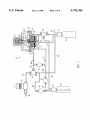
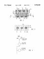
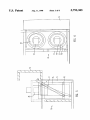
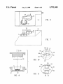
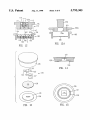
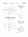
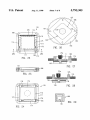
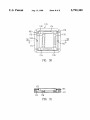
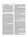
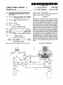
USOO5792305A
United States Patent [191
[11]
Patent Number:
Winsemius et al.
[45]
Date of Patent:
5,792,305
Aug. 11, 1993
[54] FIXTURE FOR DECAPSULATING PLASTIC
ENCAPSULATED ELECTRONIC DEVICE
PACKAGES
Primary Examiner—William Powell
Attorney, Agent, or Firm—Skjerven Morrill MacPherson
[75] Inventors: Martin L. Winsemius. Felton; Richard
A. Kanishak. Danville. both of Calif.
[57]
[73] Assignee: Nisene Technology Group. Soquel.
Apparatus for selectively etching a resinous encapsulant
wall forming an electronic device package includes etching
Calif.
[21] Appl. No.: 752,127
[22] Filed:
Nov. 20, 1996
Related US. Application Data
[63]
Continuation-impart of Ser. No. 679,222, Jul. 12, 1996.
[51]
[52]
Int. Cl.6 ...................................................... .. 1344C 1/22
US. Cl. ............................................. .. 156/345‘, 216/83
Field of Search ........................ .. 156/345 L. 345 LS.
[58]
156/637.1. 639.1; 216/38. 56. 90. 92. 83
[56]
References Cited
U.S. PATENT DOCUMENTS
4,826,556
5/1989 Kobayashi .......................... .. 216/92 X
5,443,675
8/1995 Wensink ................................ .. 156/345
Franklin & Friel; Thomas S. MacDonald
ABSTRACT
solution source; an etching assembly including an etch head
and ori?ce for directing etchant solution onto an exterior
surface of the package; a cover extending over an etch plate
mounting the etch head and forming an etching chamger; a
frame on the etch plate and in the chamber for mounting the
package such that a package exterior surface is mounted
against the etch head. the frame including a sealing gasket
between the frame and the etch head and surrounding the
ori?ce; and a ram for pushing and sealing the frame against
the etch head peripherally outwardly of and surounding the
etch head ori?ce. In a second embodiment the frame is an
etch cup having a well with or without apertures for receiv
ing package leads. In one embodiment the frame mounts a
ball grid array package, the frame including a handle per
venting contact of heated solder balls. Another embodiment
includes a universal positioner for locating one or more
devices in a device package extending over the etch head
ori?ce.
OTHER PUBLICATIONS
Model 250 Operation. Installation and Service Manual.
16 Claims, 8 Drawing Sheets
23
35
22
110
24
56
26 21
NC
45
74
US. Patent
Aug. 11, 1998
Sheet 1 of 8
5,792,305
US. Patent
Aug. 11, 1998
Sheet 2 of 8
640 630
FIG. 2
NC
3 WAY VALVE
VALVE 41
NC VALVE
VALVE 44
NC VALVE
VALVE 43
FIG. 4
5,792,305
US. Patent
Aug. 11, 1998
Sheet 3 of 8
[K [i [m
5,792,305
US. Patent
Aug. 11, 1998
Sheet 4 of 8
5,792,305
E1
FIG. 7
US. Patent
Aug. 11, 1998
Sheet 5 of 8
V///
‘M
126
5,792,305
r%/‘
/ /
FIG 14129
131
Ill
131
130
\
FIG. 13
F1 G. 15
129
US. Patent
Aug. 11, 1998
172
Sheet 7 of 8
5,792,305
FIG. 27
FIG. 25
FIG. 28
/180
172
FIG. 29
FIG. 24
174
US. Patent
Aug. 11, 1998
Sheet 8 of 8
5,792,305
170
‘85 6 Ci’)
\
I
175~
_
+
"
P
o
,175
U [ ,J
31”?‘
__ 81
172
193
171
173
178
FIG. 31
5,792,305
2
1
US. Pat. No. 5.252.179 discloses a method and apparatus
FIXTURE FOR DECAPSULATING PLASTIC
ENCAPSULATED ELECTRONIC DEVICE
PACKAGES
for selective spray etching of an epoxy encapsulated chip. A
diaphragm can be raised or lowered to direct ?ow of etchant.
and debris is removed without moving the chip from the chip
carrier. Used etchant is collected and recycled. US. Pat. No.
5.127.991 shows a process for an etching copper sheets in
which a pumped source of etchant is heated. US. Pat. No.
5.271.798 shows an etching process for tungsten residue on
This application is a continuation-in-part of U.S. Ser. No.
08/679222 ?led Jul. 12. 1996 in the name of Richard A.
Kanishak and Kirk A. Martin.
RELATED APPLICATION
This application relates to US. patent application Ser. No.
a semiconductor wafer including a sealed apparatus with an
10
Martin and entitled Decapsulator and Method for Decapsu
lating Plastic Encapsulated Device; the disclosure of which
is incorporated herein by reference.
15
FIELD OF THE INVENTION
to heat the etchant; excessive etchant fume or seepage limit
seal life; there is ine?icient removal of etching debris: a
particular slowness of the etching process is present due to
The present invention relates to an apparatus more par
non-reactive materials at the etch face; and there is a lack of
ticularly to ?xmring for holding and sealing the package and
applying an etchant to a plastic encapsulated device
package. to provide access to the device or chip for internal
etchant inlet port and suction removal of etching byproduct.
In at least some of the prior art devices various de?cien
cies have been encountered. For example. a ?xed etch head
is provided which limits the area of the package which is to
be etchant attacked; external auxiliary heaters must be used
08/656498 ?led May 31. 1996. in the name of Kirk A.
keeping acid consumption low.
20
visual inspection. test and repair.
In the related application a ?rst acid-resistant syringe
pump operates as a positive displacement pump utilizing a
standard syringe as the displacement cylinder and piston
BACKGROUND OF THE INVENTION
connected to a ?rst flow valve. To eliminate any problems
Plastic packaging of various electronic devices including
semiconductor chips have been employed for some years.
resulting from non-pulsing ?ow. a second acid-resistant
syringe pump 40 is positioned upstream of the ?rst valve and
Typical an epoxy resin is molded around the chip. a central
portion of a lead frame and bonding wires or other connec
tions between contact pads on the chip to inner lead ?ngers
on the lead frame. It is often desirous to decapsulate the
package at least in part to allow for inspection. test and
25
in connection to a ?ow line to introduce an oscillating ?ow
of etchant solution. This second pump will. during the
etching portion of the process. keep moving acid into and
30
action eventually provides the desired decapsulation of the
repair of the chip and the wire bonds to the chip and inner
lead ?ngers. after at least part of the epoxy covering these
elements is safely and effectively removed.
Commonly. concentrated acids such as sulfuric and nitric
acids or other solvents for the resin have been employed
Problems in prior art decapsulators and methods include
package.
Small outline transistors. commonly known as SOT ‘s.
35
typically have a length of about 2 mm. a width of about 1
mm and a thickness of about 0.5 mm. The epoxy encapsu
lation of an SOT typically will have a wall thickness of
about 0.25 mm. Special problems have arisen with respect to
decapsulating these very small electronic device SOT pack
ages. If the etch process is terminated only on the basis of
difficulty in controlling the desired amount of etching. in
removing debris formed in the etching process. prevention
of damage to the package including interior metallization
and providing for adequate safety.
An early patent in the decapsulator art is Wensink US.
time of etch. the entire device can be digested with attendant
damage to the small electronic device including bonding
wires and metallization.
Pat. No. 4.344.809 where a jet etch apparatus includes an
etching block and a jet pump provides for etchant ?ow.
A Decapsulator sold by B&G International. Inc. of
Soquel. Calif.. namely a Model 250. includes an appropriate
out of an etched cavity being continually formed on the
package exterior which is exposed to the etchant. and which
Prior art decapsulation etching has used negative pressure
45
on the waste side of the etch head to transport acid to the
device being etched. This process automatically terminates
acid resistant gasket seated on an etch head and the device
when an air leak is created by the side wall of the etched
to be decapsulated is placed on the gasket. A safety cover
cavity etching through. The use of negative pressure creates
a problem by causing the acid to release vapor in the etched
cavity. The vapor prevents even etching and reduces the
overall etch rate by reducing the e?icacy of the acid. This
closes automatically when the process is started, clamping
the device in place. The gasket on the etch head allows the
chamber to be sealed and pressurized with nitrogen to
approximately two PS1. The etching is started when a
metering pump moves etchant from a heat exchanger located
in plate with a sinuous passage into a cavity formed by the
gasket. the device and the etch head. The acid remains in the
chamber for a short period of time. where it reacts with or
attacks the encapsulant material. After the etchant has been
allowed to work. the pump is activated again and a fresh
volume of acid is moved into the cavity. This process
continues until the desired amount of device exposure is
achieved. When the integrated circuit is exposed at the end
of the etch cycle. the pump runs continuously to ?ush the
process will leave acid in the lines between the acid control
valves and the etch head because of the termination of all
55
mm in thickness it is known that the etching acids result in
isotropic etching. that is. the etching proceeds divergingly
from the outer surface being attacked by the acid. In contrast
anisotropic etch will result in 90° sidewalls in the etched
cavity. In isotropically etched packages the underside of the
cavity. After this rinsing period the entire system is purged
with nitrogen. blowing all waste materials into a waste
bottle. At the end of the process. the safety cover opens
automatically and the device is removed for postetch clean
ing.
acid transport when an air leak is created. This also prevents
rinsing the device being etched at the end of the etch process.
In die packages which are relatively thick such as pack
ages containing a heat sink, which packages are about 6.0
package which the acid is attacking. can be etched away so
much. when approaching or reaching the required depth of
65
etch to expose the die. that there is acid attack and break
through of the adjacent vertical sidewall(s) of the die. Thus
a need has been found for avoiding an unwanted sidewall
5,792, 305
3
4
blowout in etching apparatus such as the Model 250 Decap
there is a brealdhrough in the encapsulant allowing the
positive pressure in the bell jar to vent through the etched
sulator and other prior art devices.
opening and to the waste outlet. This action simultaneously
stops the pressurization of the acid bottle and hence the acid
flow from the bottle. ‘This action is not involved in those
?xture embodiments where the packaged device is sealed
within the ?xture.
In another embodiment an apparatus for selectively etch
ing an encapsulant forming a package around an electronic
In various medium and large size encapsulated devices
such as square encapsulated dies of 14 mm to 40 mm square
it is desirous of opening up multiple openings in the die
encapsulant or to access particular dies in a multiple chip
module. This has required in the past separate ?xturing.
Problems have also arisen in attempting the decapsulation
of very small chips having dimensions as 0.6 mm to about
1.5 mm per side or in diameter. These dimensions approxi
mate the size of a printed dot “.” in this speci?cation.
device includes an etch cup or ?xture including a demount
In the decapsulation of ball grid array (BGA) packages
using the described etching apparatus. a particular problem
to the etch head. in ?ow connection to the source of etchant
able cylindrical plug. O-ring sealed on the bottom of the etch
cup. the cup having a central passageway extending through
solution. ‘The etch head assembly may include a spiral ?ow
passage or spiral tubing for transferring heat from a resis
tance heater in the assembly to heat the ?owing acid to a
desired etching temperature. A waste passage or tube(s)
extend from the etch cavity through the assembly to the
also has arisen to avoid a ?owing of the exposed solder balls
on the package at the etching temperatures (180° C. to 240°
C.) which are present. and to avoid any contact of liqui?ed
non-?owing solder balls by any part of the etching apparatus
and ?xturing.
SUMMARY OF THE INVENTION
20
waste bottle. The electronic device package is mounted in an
etch cup or ?xture or placed directly on a surface of the etch
head facing the etching chamber.
In addition to the above. in one embodiment a ?rst
The present invention relates to an apparatus and method
for decapsulation of a packaged electronic device. more
particular a SOT or other small. medium or large package
three-way valve and an acid bottle valve is opened to
provide a positive pressure to a bell jar and an acid bottle.
encapsulating one or more electronic semiconductor device. 25 respectively. After etching a purging valve is employed to
by using a positive pressure to transport the etchant to an
etching cavity for removal *of elements of the epoxy resin
from the etch face as well as ?xturing for holding and
sealing the package with respect to an etch head. The
positive pressure effect provides an automatic cut-01f of acid
etchant ?ow and prevents any over-etching or interior
effectively rinse by ?owing pressurization gas such as
nitrogen through the purging valve into the bell jar chamber
to clear any acid remaining on the device or in the acid lines.
30
destruction or damage of the package being decapsulated.
The total cycle time is reduced while keeping acid consump
tion low. Reduced etchant heat time is also accomplished by
providing an aluminum heat exchanger block. with a spiral
The ?rst three-way valve. the acid ?ow valve and the purge
valve are provided in a combined housing. Following
completion of a cycle, another three-way valve is opened to
vent the bell jar and through the opening of the acid bottle
valve to vent the acid bottle.
The problems of the prior art of over etching causing
35
ended tube that acid ?ows through or. as in the related
damage to the electronic device can be reduced by using
positive pressure to transport the acid and to pressurize the
application an alumina ceramic. grooved cylinder heat
bell jar.
exchanger or multiple holed alumina block in ?ow connec
The etch cup ?xture provides containment for etch cavi
ties which extend beyond the sidewall being etched. The
tion to the inlet port. and an aluminum heater block con
taining at least one resistance heater. Thus only a relative
etch cup creates an arti?cial sidewall preventing acid ?ow
and positive pressure of acid into the cover cavity. When the
small volume of etchant need be heated immediately prior to
the ?ow of the etchant against the package. lessening the
package includes leads extending from the package. the
overall decapsulating time.
The apparatus for selectively etching an encapsulant
leads may be placed in a matching lead hole pattern in the
etch cup ?xture. Further. in one application the extending
forming a package of resinous material around an electronic
45
leads may be excised prior to mounting the package in the
50
contemplated inspection/test of the die which has been
encapsulated. Rubber or Te?on® blocks may be employed
to ?ll any space between the package leads or package heat
sunk extending from the package to support the leads or heat
etch cup ?xture since the leads are not necessary for the
device includes a source of etchant solution; an etching
assembly including an etch plate and an etch head having an
etch head ori?ce for directing etchant solution onto an
exterior surface of the package; a cover extending over at
least a portion of the etch plate including the etch head
ori?ce and forming an etching chamber; a frame in the form
of an etch cup or other ?xture customized for a particular IC
package i.e.. package speci?c. supported by the etch head
such that the frame holds the package against the etch head;
a sealing gasket between the frame and the etch head and
surrounding the etch head ori?ce; and a ram for pushing and
sealing the frame against the etch head peripherally out
wardly and surrounding the etch head ori?ce. An electronic
device package to be decapsulated is mounted in the cham
sink in the etch cup ?xture. In another embodiment a seal
plug and spring-actuated plunger is moved by the ram to
move a Viton® or Te?on imperforate disk against a Viton or
Te?on alignment disk having a central aperture mounting
the package and in turn to seal and push the package against
the etch head ori?ce.
In another embodiment useful when a ball grid array
(BGA) package is to be decapsulated a frame ?xture is
provided in the form of an alignment plate pocketed for ball
conduit is provided for transporting a quantity of etchant
clearance assuring that the ram nose or parts of the ?xturing
will not contact the balls which have been heated to a melt
solution from an etchant source (such as acid bottle) into the
non-?owing condition i.e.. liquify the spheres by the heated
etch head onto an adjacent abutting surface of the encapsu
lant and then forming an etched cavity on an exterior surface
during the subsequent post-etch cleaning process of the
ber on the etch head in or on the ?xture. A ?rst pressurized
of the electronic device package. Debris from the etching of 65
the package is forced through a waste outlet extending ?'om
the etch head to a waste reservoir. Etching continues until
etchant. The heated solder balls are cooled and solidify
decapsulated package.
In still another embodiment the frame ?xture is a univer
sal frame where package-holding members are movable in
5,792,305
6
5
FIG. 29 is a top plan view of the device adaptor ring.
FIG. 30 is a bottom view of the positioner showing both
both X-axis and Y-axis direction to locate a desired spacial
position on the top of a die package with respect to the etch
head ori?ce. Thus the package can be etched at any desire
spacial position or a particular die in a multi-die package can
be exposed to the etch head and for etching away a sidewall
at the location of that particular die.
the x-axis slider and a y-axis slider.
FIG. 31 is a sectional view taken on the line 3131 of FIG.
30.
DETAILED DESCRIPTION
BRIEF DESCRIPTION OF DRAWINGS
FIG. 1 is a schematic side view partially in section of the
overall decapsulation apparatus.
10
jar 22 capable of being lifted and pivoted by structure (FIGS.
FIG. 2 is a cross-sectional side view of the combined
7 and 8) onto the etch plate 21. The interior of the bell jar
forms an etching chamber 30. A spring pressed holder 23
valves and housing.
FIG. 3 is a bottom view taken on line 3—-3 of FIG. 2 and
top view of the valve block thereof.
FIG. 4 is a schematic sketch of the interconnections of the
valves in the combined housing.
FIG. Sis a side view partially in section of a containment
housing for the acid and waste bottles.
FIG. 6 is atop view thereof with the cover also in the open
condition.
FIG. 7 is a side view partially in section of the overall
15
20
with a ram nose 23a holds the SOT electronic device
package 3 to be decapsulated against the etch cup or ?xture
or against an etch head top surface 25a and is sealed thereto
by a gasket or seal 5. The etch head 25 includes an etchant
solution inlet passage 11 and waste outlet passages 12
leading to a waste tube 15 extending through a bore in a heat
exchanger block 26. Block 26 abuts the bottom of the etch
head 25 and includes a spiral passageway 27 on its underside
for receiving spirally-formed tubing 17 for heating etchant
solution ?owing through the tubing passageway. A heater
device showing the bell jar mounting procedure.
FIG. 8 is a top view thereof.
FIG. 9 is a cross sectional view of an etch cup and plug
embodiment.
FIG. 10 is a bottom view of the heat exchanger block.
FIG. 1 shows a decapsulating system 10 including an etch
head assembly 20 including an etch plate 21. an integral etch
head 25 centrally of the plate. and a movable cover or bell
25
block 28. including one or more resistance heaters 29. abuts
against the bottom spiral tubing 17 and the heat exchanger
block 26.
When no process is running. valve 41 is off. shutting oh‘
the low pressure to the entire unit. Valve 42 is open venting
the acid bottle 36 and valve 45. is off. also venting the acid
bottle. When an etch process is started. valves 41. 42 and 45
are activated allowing the bell jar and the acid bottle to
pressurize to about 2 PSI. When valve 43 opens. the N2
pressure through line 54 forces the acid from the bottle 36
FIG. 11 is a top view of the heater block showing the
surface interfacing with the surface shown in FIG. 10.
FIG. 12 is an exploded cross-sectional view of another
embodiment of the etch cup and plug ?xture.
FIG. 12A is an exploded cross-sectional view of a vented
etch cup.
35 through line 37a. through open valve 43. through line 37b.
through a venturi ?ow reslrictor 37 that controls acid ?ow
FIG. 13 is an exploded perspective view of an etch cup
volume.
through the heat exchanger or other reservoir and
fixture for a transistor package.
through inlet passage 11 to impinge on the device to be
FIG. 14 is a cross-sectional view of the plug portion.
etched. Acid will continue to ?ow as long as the device is
FIG. 15 is a bottom view of the plug portion.
sealed to the etch head.
FIG. 16 is a top view of a ball grid array package ?xture.
As soon as a verticle side wall. Le. a wall not including the
surface being etched. of the package by formation of the
FIG. 17 is a cross-sectional view thereof taken on the line
etched cavity is etched through. Le. a break-out occurs. the
pressure inside the bell jar vents through outlet passage( s) 12
17-17 of FIG. 16.
FIG. 18 is a bottom view thereof.
FIG. 19 is a cross-sectional view of the plug portion of an
etch cup ?xtm'e for an extended leads package decapsula
tion.
FIG. 20 is a bottom view thereof.
FIG. 21 is a cross-sectional view of the etch cup portion
of the ?xture.
FIG. 22 is a top plan view thereof.
FIG. 23 is a top view of a universal positioner ?xture
showing an x-axis slider.
FIG. 24 is a top view thereof showing the stacked y-axis
slider.
FIG. 25 is a cross-sectional view taken on the line 25-25
of FIG. 23 show a vertical adjustment mechanism.
FIG. 26 is a top plan view showing a positioner template
oriented to an etch head ori?ce.
FIG. 27 is a schematic cross-sectional view of the x-axis
slider with mounted etch cup. a package to be decapsulated.
45
55
to the waste line 15 and to waste bottle 33 or other reservoir.
This also increases the pressure in the acid lines 11. 37c. 17.
37b and 37a and reduces the pressure in the acid bottle. This
increased pressure. when it reaches restrictor 37 essential
blocks acid ?ow to the etch head. This prevents any further
flow of acid. At the end of the etch process. valve 43 is
allowed to close and valve 44 is opened. This pressurizes the
acid carrying tubes 17 in the heat exchanger to greater than
the pressure at the etch head and purges the heat exchanger
of acid. This purge also rinses any remaining etch debris
from the device being etched or in passage 12 and line 15 to
waste bottle 33. Also. the valve 45 is positionable to connect
the acid bottle 36 through line 39 to waste bottle 33 with
valve 43 closed to vent the acid bottle 36.
The pressurization of the acid bottle 36 can only happen
when the bell jar 22 is down on the etch plate and sealed
thereon by seal 24. This prevents any possibility of acid
transport when the etch head is exposed. The acid bottle is
vented through both valve 42 and 45. requiring both valves
gasket. etch head and pressure ram.
to fail in the active state for pressure to remain in the acid
FIG. 28 is a schematic cross-sectional view of the x-axis 65 bottle. ‘The bell jar itself with a venturi ?ow restrictor 54 in
line 54a. operates as a pressure relief valve. The closing
slider for a ball grid array package. showing protection of
pressure on the bell jar is limited to about 45 pounds. If the
the solder balls from ram pressure.
5.792.305
7
8
pressure inside the bell jar exceeds about 3 PSI. the bell jar
bottles. A secondary containment is provided by a PVC pipe
will lift slightly venting the excess pressure across seal 24.
As the pressure to the acid bottle is supplied from the bell jar.
this limits the maximum pressure in the acid bottle 36.
75 surrounding each of the bottles and glued to a movable
liftable plate 76 connected by arm 77 to cover 72. Upon
Additionally. both the source and waste bottles are fully
enclosed each in its own secondary containment chamber. as
seen in FIGS. 5 and 6.
An etchant solution. such as nitric acid. in particular
for ease of access. The dashed lines show the cover closed
fuming nitric acid. is utilized as an etching agent.
A standard low pressure regulator 53 such as Part No.
101-3008-1. available from Monnier C0. of Algonec. Mich.
cover where cover ‘77 covers the acid bottle and a robotic
opening the cover. plate 76 rises moving the bottles upward
and the plate 76. pipe 79 and bottles “down” in the housing
70.
FIG. 7 illustrates another embodiment of the acid bottle
actuator 78 moves the bell jar 22 from an etch position A to
a raised. o?’set position B for placement of and removal of
supplies the nitrogen gas for acid ?ow and for purging.
About 40 psi of nitrogen gas is supplied (not shown) to
operate the pneumatic controls (not shown) for the various
the encapsulated and decapsulated electronic device.
valves. Valves 41. 42. 43. 44 and 45 may be Te?on®
diaphragm pneumatically actuated valves as shown in FIG.
2.
To effectively transport etch debris and create a clean
cavity. a flow rate of about 3 to about 5 ml per minute of acid
etch head 25 (FIG. 1). A circular aperture 82 allows access
of acid to a device 3 to be decapsulated. mounted in the cup.
The device 3 is sealed by annular seal 5 as in FIG. 1. A
is required. This is supplied by adjustment of the nitrogen
of plug 83.
pressure so that the inert gas pressure is between about 1.5
FIGS. 10 and 11 illustrate the interface between heat
exchanger block 26 and heater block 28. The underside of
heat exchanger block 26 in FIG. 10 includes a milled spiral
groove 27 (dashed lines) which extends from a peripheral
edge entry 86 to a milled entry port 87 of an oval integral
Te?on® extension 88. depending from block 26 (FIG. 1).
Tubing 17 extends along the grooves 27. The extension
FIG. 9 illustrates one form of a cylindrical PTFE Te?on
etch cup 80 having a bottom surface 81 which seats on the
cylindrical Te?on plug 83 is press-?tted into the cup with an
O-ring seal 84. The ram nose 23a presses down on the top
psi to about 3 psi. The acid and waste bottles typically are
constructed of Te?on molded plastic or glass.
The etching procedure. in general. comprises 1) opening
25
valves 41 and 45 and closing valve 42 to pressurize both the
interior of the bell jar 23 and the acid bottle 36; 2) valve 43
is intermittently activated (opened) to pulse the acid ?ow to
reduce acid consumption and to allow acid ?ow to the
includes a pressurizing hole 89. a waste outlet hole 90 and
a vent hole 91. and bolt holes 92 for assembly with the heater
encapsulated package 3; 3) etching continues until break-out
block 28. Facing the extension 88 is the aluminum heater
block 28 which includes an oval slot 92 for press-?tted
of the eneapsulant; 4) when break-out occurs the bell jar
pressure and the acid bottle pressure vent through the
break-out to the waste lines. automatically stopping the acid
flow and further etching; 5) valve 43 is then closed and valve
reception of the extension 88. Milled slots 93 are provided
for a connector part of the resistance heaters. and are
provided on opposite sides of the slot 92. The slots 93 lead
44 is opened clearing the acid lines by N2 pressure while
to a rectangular milled areas 94 of about 0.25 mm deep. into
momentarily opening valve 43 to purge all the acid back to
bottle 36; and 6) at the end of the cycle. valve 45 is closed
and valve 42 is opened to vent the acid bottle. Valve 41 is
closed to shut off the N2 ?ow and vent the bell jar. Tubing
line 46 extends between valve 41 and the waste bottle 33 to
vent from the acid bottle through open valve 42 and line 38.
and to vent the bell jar.
FIG. 2 and 3 illustrate a single combined housing 60 for
valves 41. 44. and 43. First rectangular housing member 61a
includes three spring valve closure members 63 including a
spring guide 630. Arectangular valve block 64 contains the
valve seats and ?ow passages. A second rectangular housing
member 61b seats on valve block 64. A rectangular valve
which rectangular ?at “pancake” resistance heaters 96 are
placed. Bolt holes 95 match bolt holes 92 in block 26 and are
aligned when extension 88 is placed in the slot 92.
In the decapsulation process using the above described
apparatus. the etch may be a timed etch. for example. for 30
seconds but. if for any reason such as a thinner package wall
or excess etching attack. the integrity of a package wall is
broken prior to the 30 seconds. the 2 psi pressure in the bell
45
jar will vent to the waste lines 12. 15 above seal 5 (FIGS. 1
and 9) stopping all ?ow from the acid bottle. Seal 5 only
seals the IC package surface which faces the etch head or the
bottom of the etch cup. if such a ?xture is being used
A small local processor (not shown), such an a PIC 16C55
cover 65 is sealed by gaskets 66 to housing member 61b.
Each valve includes an activation diaphragm 67 which
processor available from Microchip Technologies of
moves an actuator 68 and diaphragm stem 69a into abutment
with a diaphragm stem 69b attached to a diaphragm 69d
Chandler. Ariz.. as is known in the art is used to control the
valve functions. The control electronics are distributed
which is spring pressed inwardly by spring guide 63a and
between the multi-controller and the processor in the etcher
unit. The rnulti-controller provides the user interface and the
spring 63. Air pressure enters the chamber. housing dia
phragm 67. through aperture 65b. A push-pull operation of
the diaphragm stems permits pressure ?ow through central
supervisory control of the etcher unit. A temperature control
sub-processor (not shown) measures the output of the resis
passage 640 from valves 41. 44 and 43. the full diameter of
the items blocking N2 ?ow and the tapered ends of the stems
tance heater. ambient temperature. line voltage. and current
permitting N2 ?ow. FIG. 4 shows the various positions of
the di?erence between the desired temperature of the heat
three-way valve 41 namely NO standing for ljorrnal
Qpen. COM standing for Common. and NC standing for
exchanger and the actual temperature thereby controlling the
heat exchanger temperature. A multi-controller (not shown)
into the heaters. It adjusts the current into heaters based on
is used to send commands to the local processors and the
local processor performs the actual valve and temperature
FIGS. 5 and 6 illustrate a protective housing 70 for the
control.
acid and waste bottles including a rectangular housing 71. a
Etchant selection. safety equipment for the operator. unit
hinged cover 72 and an acid bottle manifold 73 and waste 65
set-up details of a typically used controller modi?ed for use
bottle manifold 74. such that when the cover 72 is closed the
with the valve system of the invention. and general mechani
cover acts as a safety cover for each of the acid and waste
Eormal Qlosed.
5 .792.305
9
10
cal and electrical operations of a typical decapsulator are in
the Model 250 Operation. Installation and Service Manual.
the content of which are incorporated herein by reference.
All components. other than springs. screws. and selected
valve components. are made of Te?on® plastic. glass.
(FIG. 19) with the etch cup 144. As in the earlier
embodiment. plug number 141 containing the device pack
age is slid into cavity 147 of cup 144 and an integral
depending ring 146 seals the cup to the etch head de?nition
gasket. The cup 144 ?ts snugly over the etch head outer
diameter.
PIGS. 16-18 show a ?xture for a plastic ball grid array
polypropylene. or PVC or other acid-resistant material. The
only metal components utilized are the springs and screws
which. where possible. are made of stainless steel. All ?ve
valves are pneumatically activated when decapsulation is
being performed as described above. All manifold ports are
the standard l/4-28 thread.
FIG. 12 illustrates a varient of the etch cup ?xmre seen in
FIG. 9. An electronic device package 3 in mounted within a
circular etch cup 100. particularly in a central aperture 102
of a Viton® or Te?on® circular alignment gasket 103 placed
against a bottom etch cup wall 105 in a ?rst cavity 104 of the
etch cup. The bottom etch cup wall 105 is apertured at 106
to receive acid ?ow from the etch head ori?ce 27 (FIG. 1).
A circular blank (unapertured) Viton or Te?on disk 107.
notched at 107a on its periphery for easy removal by a
tweezer or pry implement. covers alignment gasket 103.
Plug 110 slides into the cavity 104. Plug 110 includes a
(PBGA) package (illustrated as package 136 in FIG. 28)
which has package contact pads on the surface of the
10
overforce on the disk gasket and the package 3 in cavity 102.
while e?’ectively sealing the die package 3 except at the
aperture 106 through which the etchant ?ows. An O-ring
may be placed in groove 117. The etch cup 100. plunger 110
and other elements may be of various sizes. shapes and
thicknesses to accommodate various sized device packages.
FIG. 12A shows a vented etch cup assembly including etch
by etching. in the form of solder balls. A?xture 150 includes
an alignment plate or frame 151 specially pocketed for
solder ball clearance. The rim or peripheral edge of the
PBGA matches an internal mm 153 of the frame 151. The
15
20
PBGA is placed into the pocket 154 from the underside of
the frame (arrow 160). The halls face upward directly under
the plane of the frame top surface and spaced vertically
under a 90° angle bar 155 spanning the frame pocket and
connected to the frame by fasteners 149. The PBGA may be
held in the pocket preventing drop out by a I/:" (0.64 cm)
strip of Kapton® tape (not shown) on opposite sides of the
PBGA adjacent to the PBGA underside wall to be decapsu
lated by etching. Aram 230. as in FIG. 1. presses against the
horizontal portion 156 of angle bar 155 which with the
plunger 111 having an upper end 112 which is pressed by
spring 114 and ram 23a against disk 107 and in turn against
alignment gasket 103 to seal cavity 102. A ?ange stop 115
acting against ?ange 116 of the etch cup 100 prevents any
package opposite the package side wall to be decapsulated
25
alignment plate distributes the compressive force around the
PBGA edges and seals the frame with the cavity de?nition
gasket provided on the etch head as in the other embodi
ments. The vertical portion 157 of the angle bar serves as a
30
handle for removal of the ?xture from the etch head. using
tweezers or the like. After etching has decapsulated the
PBGA. it is preferred to leave the device in the frame until
after post-etch solvent cleaning. The back (top) of the
package containing the balls is completely protected and the
decapsulated device package is in an opened condition on
cup 100 and a modi?ed plug 100a and where apertures 119
the underside of the ?xture so that the device can be tested
and the absence of blank 107 allows for venting of the 35 and inspected. Alignment apertures 158 and 159 are pro
positive pressure in the bell jar 22 (FIG. 1) to stop acid ?ow
vided which with pins (not shown) on the etch plate.
properly align ?xture 150 with respect to the etch head.
FIGS. 23-26 and 30-31 illustrate a universal positioning
?xture 170 including a frame 171 which is capable of
when a chip sidewall is breached. Aram 23a is pushed down
through aperture 119a to hold the chip against the top edges
of acid aperture 106.
FIG. 13-15 illustrate an etch cup kit 120 for decapsulating
a transistor package 121 while providing containment for
extended cavities beyond the package side walls. The tran
sistor package 121 normally includes a die section 122. a
heat sink 123. and leads 124 extending therefrom. The
device package is placed in well 125 (FIG. 14) of the etch
cup 126 after leads 124 have been excised. Rubber or Te?on
blocks 127 may be positioned. after the package has been
placed in well 125. to ?ll the space between the package heat
sink and the etch head 131 in the etch plate 130. Ade?nition
gasket 128 may be used to reduce the initial etch cavity size
accurately locating medium (about 14 mm maximum length)
to large (about 40-63 mm maximum length) sized devices to
relieve the ongoing demand for custom ?xturing. This
?xture is expressly designed for multiple chip modules in
45
and slides provided can ?oat with adjustable friction or be
locked down for repeated usage. Components are made of
50
produced by the etching action. In this embodiment. the etch
cup 120 further includes an integral depending ring 129 for
sealing against the etch head 131. The well 125 acts as a
Te?on box creating an arti?cial side wall preventing the
etchant from exiting into the interior of hood cover 22 (FIG.
The embodiment disclosed provides for a device dimension
plus offset outlines up to 63 mm (2.50 inch) square; PBGA.
55
FIGS. 19 and 20 show a ?xture to decapsulate a dual-in
line package (DIP) or other array of leads extending from a
side or edge of the package opposite to the package side wall
to be etched. The well 140 in the etch cup cap 141 is
QFP. TQFP. DIP. SIP (single inline plastic) and PLCC
packages are easily accommodated; accuracy and repeat
ability of 0.2 mm (0.008 inch) is possible; and a 0.1 cm
graduated scale is supplied for user reference and adjust
ment.
As seen in FIG. 26 a sheet metal such as a stainless steel
sheet metal template rectangle 188 is placed ?ush on the etch
plate adjacent to etch head 130. locating the positioner on
center to the etch head. Pins 187 extend from the etch plate
189 through apertures 190. one aperture being oval and the
other circular. The edges 191 of the template abut a rim 192
provided with apertures 142 matching the lead pattern of the
package to be decapsulated. The etch cup surface mating
with the de?nition gasket may be lightly coated with high
reduce acid damage. A location pin 145 (FIG. 21) is
employed to accurately align hole(s) 143 in the cap 141
corrosion-resistant materials such as Te?on and stainless
steel. Fixturing is easily disassembled for routine cleaning.
1).
vacuum grease available from Dow Corning Chemical Co.
of Midland. Mich. Device leads may be similarly coated to
PBGA. QFP (quad ?at pack). TQFP (thin QFP). D11’. SIP
and PLCC (plastic leaded chip carrier) packages. These
multiple-die packages require ?exible ?xtun'ng and 01T
center alignment capabilities. Operator setups are simple
65
on the etch plate 185. the rim also forming a side wall of a
gasket groove surrounding the rim. The template is left on
the etch head and the ?xture is mounted thereon.
5 ,792,305
12
11
surface of the package is mounted against said etch
head. said frame including a sealing gasket between the
frame and the etch head and surrounding the etch head
ori?ce; and
a ram for pushing and sealing said frame against said etch
head peripherally outwardly of and surrounding the
etch head ori?ce.
The frame 171 supports two pairs of parallel guide shafts
172 and 173 and two pairs of parallel sliders 174 and 175 on
the shafts for x and y axis of travel. Each slider can be
positioned independently. allowing either centered or offset
device package alignment. The sliders glide on Te?on guide
5
pieces or ends 176 at each comer of each of the x-axis and
y-axis corners of the sliders where they engage and slide on
the guide shafts. Each slider also has an adjustable plunger
2. The apparatus of claim 1 wherein said frame is an etch
or set screw 178 and 179 used to tension or lock the slider
cup. said cup including a cavity for insertion of the package
into an open end of the cup in ?ow connection to said etch
when the desired position is reached. Screws 193 passing
through the frame (FIG. 30) prevents the rods from bowing
head ori?ce and the exterior surface of the package facing
said etch head ori?ce. said cup having sidewalls which
prevent etchant solution from reaching said etching cham
or moving outwardly. The frame 171 is specially located on
the etch head by screws 186 ?tting into holes adjacent to the
etch head. The x and y sliders are moved outward leaving a
“drop-in" space for a device package of various exterior
dimensions.
15
said well being sized to receive the package.
4. The apparatus of claim 3 further including spaced
As seen in FIG. 27 most package types will employ an
alignment adapter 180 with the appropriate size opening 181
on center (FIG. 29) into which the device 3 (FIG. 27) is
inserted. The adapter is preferably constructed of aluminum
material and functions to facilitate the location of the device
apertures in said well for receiving package leads extending
from the package.
20
package. Alarge device package such as a long DIP. may be
better aligned without an adapter. The adapter (or device)
6. The apparatus of claim 3 wherein the package includes
an exposed heat sink extending laterally from the package.
adaptor 195 for the decapsulation of a PBGA 136 in FIG. 28.
APBGA requires a closed back alignment adaptor 195 (FIG.
28) to distribute the sealing force around the package edges
Engraved scales 185 (one shown in FIG. 23) with indicia
lines and numbers thereon are provided to indicate the axial
position of each slider from center. The ?xture is inverted to
access to the lower y-axis slider pair. The removable scale
plates are placed in position temporarily to establish desired
locations. Settings should be recorded for future reference.
30
9. The apparatus of claim 2 further including an etch cup
plug movable into said cavity and forming said planar top
35
surface.
10. The apparatus of claim 9 wherein said plug includes
a spring plunger for sealing said cavity.
11. The apparatus of claim 9 wherein said plug includes
a venting aperture for venting a positive pressure in the
etching chamber when a package side wall is breached by
?ipped back over to set up the upper (x-axis) slider pair in
the same way. The positioner assembly is placed on the etch
plate by engaging elevator screws 186 into template location
slots 148. The vertical position of the ?xture is adjusted with
the etchant solution.
12. The apparatus of claim 1 wherein said frame com
the four elevator screws 186 as required.
prises a central opening having a bottom peripheral ridge
45
fit is provided allowing small clearances between sliders and
the adapter ring sides so that vertical travel is not obstructed.
The available positioning area is designated by the dash line
rectangle 177 in FIG. 23.
The above description of the preferred embodiments of
this invention is intended to be illustrative and not limiting.
Other embodiments of this invention will be obvious to
those skilled in the art in view of the above disclosure.
We claim:
1. An apparatus for selectively etching a portion of an
encapsulant forming a package of resinous material around
said well being sized to receive the package.
7. The apparatus of claim 6 further including support
blocks ?lling a space between the heat sink and the etch
head.
8. The apparatus of claim 3 wherein said etch cup
comprises a planar top surface. said ram contacting said
planar top surface.
Sliders may be tensioned or locked into position to resist
accidental movement by set screws 179. The ?xture is
After the appropriate cavity de?nition gasket 128 is
selected and installed. the device adaptor and device pack
age is placed into the region inside the ?xture sliders. Proper
5. The apparatus of claim 3 wherein said etch cup open
end includes an aperture de?nition disk for directing etchant
solution from the etch head ori?ce to the exterior surface of
the package.
edges are located by the positioner sliders. The etch ram
nose 23a as seen in FIGS. 27 and 28 apply sealing pressure
to the device package either directly in FIG. 27 or by the
via the pocketed device alignment adapter.
ber.
3. The apparatus of claim 2 in which said etch cup
includes a package well in an interior surface of the etch cup.
and where a plastic ball grid array package is mountable on
said ridge from an underside of the frame and solder balls on
the package extend below a top plane of said frame.
13. The apparatus of claim 12 further including an angle
bar extending across the frame central opening connected to
a top surface of the frame.
50
55
14. The apparatus of claim 1 wherein said frame includes
a ?rst pair of parallel slider shafts extending across said
frame; a second pair of parallel slider shafts extending
across said frame at right angles from said ?rst pair of
parallel shafts; a ?rst pair of sliders slidable on said ?rst pair
of parallel shafts; a second pair of sliders slidable on said
second pair of parallel shafts; and wherein a device package
is mountable between said pairs of sliders and said sliders
an electronic device comprising:
a source of etching solution;
an etching assembly including an etch plate and an etch
are movable on said shafts to specially locate the device
package on a position exposed to the etch head ori?ce.
15. The apparatus of claim 1 further comprising a tem
head having an etch head ori?ce for directing etchant
solution onto an exterior surface of the package;
plate for specially locating said frame with respect to said
etch head ori?ce. said template extending between an under
a cover extending over at least a portion of the etch plate
side of said ?'aine and the etch plate and etch head.
16. The apparatus of claim 15 further including an adapter
including the etch head ori?ce and forming an etching
chamber;
a frame positioned on said etch plate and in said chamber.
said frame mounting the package such that an exterior
65
inside said frame and above the sealing gasket.
*
*
*
*
*