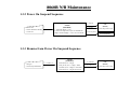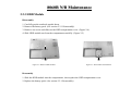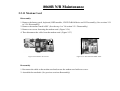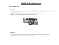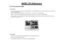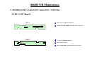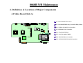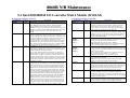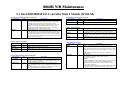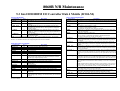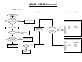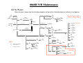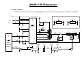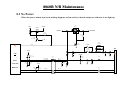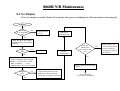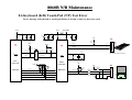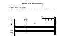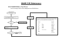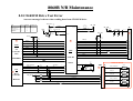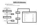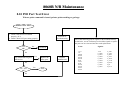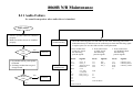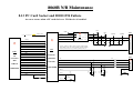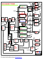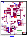
1
SERVICE MANUAL FOR
8060B
BY: Sissel Diao
Repair Technology Research Department /EDVD
Jun. 2003
8060B N/B Maintenance
Contents
1. Hardware Engineering Specification …………………………………………………………………
4
1.1 Introduction …………………………………………………………………………………………………………. 4
1.2 System Architecture ………………………………………………………………………………………………… 6
1.3 Electrical Characteristic …………………………………………………………………………………………… 19
2. System View and Disassembly ………………………………………………………………………...
29
2.1 System View ………………………………………………………………………………………………………… 29
2.2 System Disassembly ………………………………………………………………………………………………… 32
3. Definition & Location of Connectors / Switches ……………………………………………………..
57
3.1 Mother Board ……………………………………………………………………………………………………….. 57
3.2 Audio DJ Board …………………………………………………………………………………………….……… 60
3.3 DC to DC Board ……………………………………………………………………………………………………. 61
4. Definition & Location of Major Components ………………………………………………………..
62
4.1 Mother Board ……………………………………………………………………………………………………….. 62
5. Pin Description of Major Component …….………………………………………………………….
64
5.1 Intel Pentium M Processor ………………………………………………………………………………………… 64
5.2 Intel 82855GM Memory Controller Hub (Odem) ……………………………………………………………….. 68
5.3 Intel 82801DBM I/O Controller Hub 4 Mobile (ICH4-M) ………………………………………………………. 74
1
8060B N/B Maintenance
Contents
6. System Block Diagram ………………………………………………………………………………..
82
7. Maintenance Diagnostics ………………………………………………………………………………
83
7.1 Introduction ………………………………………………………………………………………………………… 83
7.2 Error Codes …………………………………………………………………………………………………………. 84
7.3 Maintenance Diagnostics …………………………………………………………………………………………… 87
8. Trouble Shooting ………………………………………………………………………………………
88
8.1 No Power …………………………………………………………………………………………………………….. 89
8.2 No Display …………………………………………………………………………………………………………… 94
8.3 VGA Controller Failure LCD No Display ………………………………………………………………………… 97
8.4 External Monitor No Display ……………………………………………………………………………………… 99
8.5 Memory Test Error ………………………………………………………………………………………………… 101
8.6 Keyboard (K/B) Touch-Pad (T/P) Test Error ……………………………………………………………………. 103
8.7 Hard Driver Test Error ……………………………………………………………………………………………. 105
8.8 CD-ROM Driver Test Error ………………………………………………………………………………………. 107
8.9 PIO Port Test Error ………………………………………………………………………………………………… 109
8.10 USB Port Test Error ………………………………………………………………………………………………. 111
8.11 Audio Failure ……………………………………………………………………………………………………… 113
8.12 LAN Test Error …………………………………………………………………………………………………… 116
8.13 PC Card Socket Failure ………….……………………………………………………………………………….. 118
2
8060B N/B Maintenance
Contents
9. Spare Parts List ………………………………………………………………………………………..
120
10. System Exploded Views ………………………………………………………………………………
133
11. Circuit Diagram ………………………………………………………………………………………
134
12. Reference Material …………………………………………………………………………………...
164
3
8060B N/B Maintenance
1. Hardware Engineering Specification
1.1 Introduction
1.1.1 General Description
This document describes the system hardware engineer specification for 8060B portable notebook computer
system.The 8060B notebook computer is a new mainstream high performance thin and light notebook in the MiTAC
notebook family.
1.1.2 System Overview
CPU
- Mobile Intel Banias, 1.3-1.7GHz or above
- 1MB L2 Cache
Core logic
- Intel 855PM (Odem) + Intel 82801DMB (ICH4-M)
System BIOS
- Insyde 512KB Flash EPROM
Memory
- 0MB Memory onboard ; Expandable to 1.0GB
- 200-pin DDR Memory Slot x2, DDR-200/266 specifications (USER Upgradeable)
VGA Controller
- nVidia NV34M; Support AGP4X
- Discrete 64MB DDR VRAM (reserve for 128MB)
IDE
- Support 2 IDE channel, Up to Ultra DMA 100
LCD Display
- 15.2” TFT display; 15:10 wide screen, Resolution 1280 x 854 WXGA+
Keyboard
- Internal Key Matrix Keyboard
Touch Pad
- Intelligence Glide pad with 2 buttons.
- Include System BIOS, VGA BIOS
4
8060B N/B Maintenance
Continued to previous page
Audio
- Built-in AC97 V2.2 Codec
- Sound Blaster Pro compatible
- 3D stereo enhancement
- Built-in mono microphone
- Built-in 22W / 3ohm stereo speakers
Audio DJ
- 4 player buttons: Play/Pause, Next Track, Previous Track, Stop/Eject (support System Power-off play)
- 1 push button and 1 LED for Audio DJ function On/Off (Push 1 second for turn-on, toggle for turn-off)
- Automatically turn-off for CD player idle more than 5 minutes
- Digital volume Up/Down control
PCMCIA
- Type II x1 or Type I x1; CardBus support
I/O Ports
- Bi-directional Parallel port (EPP/ECP) x 1
- USB (support USB 1.1 and USB 2.0) port x 3
- RJ-11 port x 1
- RJ-45 port x 1
- DC input x 1
- Battery Connector x1
- VGA monitor port x 1
- Line-out (SPDIF) x 1
- Mic-in x 1
- Line-in
- IEEE1394 x 1
- FIR/SIR x 1
- TV-Out x 1 (7Pin S-Video connector NTSC/PAL)
MiniPCI
- 802.11b wireless LAN (optional) with built-in Antenna
LAN/MDC
- 10/100 Base-T LAN
Suspend Mode
- POS (S1), Suspend to RAM (S3), Suspend to Disk (S4), Non support Wake Up on time
LED Indicator
- HDD, CD-ROM, NUM, CAP, SCROLL, Wireless LAN, Audio DJ PWR
- Non support Zoom Video/Audio Function
- MDC 56K, V.90 Modem
5
8060B N/B Maintenance
1. .2 System Architecture
1.2.2 Function Description
1.2.2.1 CPU
Mobile Intel Banias processor with 400MT/s BPSB (100MHz)
Capable of 478-pin, Micro-FCPGA processor package
On-die 32KB instruction cache and 32KB write-back data cache
On-die 1MB L2 cache
Assisted Gunning Transceiver Logic (AGTL+) bus driver technology
1.2.2.2 Core Logic
Intel 82855PM Memory Control Hub
- Support AGP2.0 (4X AGP)
- Support 200 and 266 MHz DDR devices
- Maximum of 1GB of system memory by using 512MB technology devices
- Hub Interface to ICH4-M
Intel ICH4-M I/O Controller Hub
- PCI 2.2 Interface
- Bus Master IDE controller supports Ultra ATA 100/66/33
6
8060B N/B Maintenance
- AC’97 2.2 Interface
- USB 1.1 and USB 2.0 Host Controllers
1.2.2.3 Memory
Support 200/266MHZ SO-DIMMs DDR Memory expandable to 1024MB (2 SO-DIMM DDR slot).
Slot1
Slot2
Total
64MB
64MB
64MB
64MB
64MB
128MB
128MB
128MB
128MB
256MB
256MB
256MB
512MB
512MB
0
64MB
128MB
256MB
512MB
0
128MB
256MB
512MB
0
256MB
512MB
0
512MB
64MB
128MB
192MB
320MB
576MB
128MB
256MB
384MB
640MB
256MB
512MB
768MB
512MB
1024MB
Table 1. Memory Expansion Capacity
7
8060B N/B Maintenance
1.2.2.4 I/O Ports
CRT Port
- Standard VGA compatible port
- DDC1 and DDC2B compliant
Pin
Signal
Description
1
2
3
4
5
6
7
8
9
10
11
12
13
14
15
RED
GREEN
BLUE
Monitor Sense
GND
GND
GND
GND
VCC
GND
Monitor Sense
CRT DATA
HSYNC
VSYNC
CRT CLK
Red analog video output
Green analog video output
Blue analog video output
Monitor Sense
Ground
Ground
Ground
Ground
+5VDC
Ground
Monitor Sense
Data from DDC monitor
Horizontal Sync control
Vertical Sync control
Clock to DDC monitor
Figure 1. CRT Connector
Table 2. CRT Connector
8
8060B N/B Maintenance
7 Pins S-Video port for TV-Out
- Support up 1024*768 resolution
- Support PAL and NTSC system
- Support Composite Output by a transfer cable
Pin
1
2
3
4
5
6
7
Signal Name
Description
GND
NC
COMP
GND
CRMA
NC
LUMA
Table 3. S-Video Port
O
O
O
System
Input(Active) Resolution
Active TV Lines
Over/Under Scan
NTSC
NTSC
NTSC
NTSC
NTSC
NTSC
320 x 320
640 x 480
720 x 480
720 x 400
800 x 600
1024 x 768
480 ~ 400
480 ~ 400
480 ~ 400
480 ~ 400
480 ~ 420
480
+
+
+
+
+
Over
System
Input(Active) Resolution
Active TV Lines
Over/Under Scan
PAL
PAL
PAL
PAL
PAL
PAL
320 x 320
640 x 480
720 x 480
720 x 400
800 x 600
1024 x 768
540 ~ 500
540 ~ 500
540 ~ 500
576 ~ 510
600 ~ 510
520
+
+
+
+
+
Under
Table 4. TV Out Support Modes
9
8060B N/B Maintenance
IEEE 1394 Port
- Supports serial bus data rates of 100, 200, and 400Mbits/second
- The Asynchronous and Isochronous data transfers are supported
- One IEEE1394 port supported
Pin
Signal Name
Description
1
2
3
4
TPBTPB+
TPATPA+
I/O
I/O
I/O
I/O
Table 5. IEEE1394 Port
Figure 2. 1394 Connector
Audio Ports
- SPDIF
- Microphone In & Line In
- Built In 2 high quality internal speaker (1W / 8 ohm with Box)
- Built in 1 mono microphone
- AC97 V2.2 compliance.
Plug Ear-Phone In
Plug SPDIF Device In
Plug External Microphone
Internal Speaker
Internal Microphone
LED of SPDIF
Mute
Mute
Mute
Active
Active
Mute
Off
On
Off
10
8060B N/B Maintenance
RJ-11
- Connection to Modem Daughter Board Connector
- Support 56Kbps/V.90
Pin
1
2
3
4
Signal Name
NC
LINE +
LINE –
NC
Direction
Description
I/O
I/O
-
No Connect
Phone Line Positive
Phone Line Negative
No Connect
Table 6. Modem Port
Figure 3. Modem Connector
RJ-45
- Support full duplex 10 Base-T, 100 Base-T Ethernet
Pin
1
2
3
4
5
6
7
8
Signal Name
TX +
TX –
RX +
TERM 1
TERM 2
RX
TERM 3
TERM 4
Direction
Description
OUT
OUT
IN
IN
-
Transmit Data Ring
Transmit Data Tip
Receive Data Ring
Internal termination resistor
Internal termination resistor
Receive Data Tip
Internal termination resistor
Internal termination resistor
Table 7. LAN Port
Figure 4. LAN Connector
11
8060B N/B Maintenance
Infrared interface supporting IRDA format
- FIR IrDA 1.1 compliant.
- HP-SIR supported.
USB Ports
- Three industry standard USB 2.0 ports
- Support MAX. Power Current 500mA each port
Pin
1
2
3
4
Signal Name
VCC
DATADATA+
GND
Direction
Description
I/O
I/O
-
USB Device Power (+5VDC)
Balanced Data Negative
Balanced Data Positive
Ground
Table 8. USB Port
Figure 5. USB Connector
Parallel Port
- Configurable as logical ports LPT1 , LPT2 or LPT3
- EPP rev 1.7 & 1.9 compatible
- ECP (IEEE 1284) compatible
- Industry standard 25 Pins connector
12
8060B N/B Maintenance
Pin
Signal Name
Direction
Description
1
2
3
4
5
6
7
8
9
10
11
12
13
14
15
16
17
18
19
20
21
22
23
24
25
Case
STROBE#
PD0
PD1
PD2
PD3
PD4
PD5
PD6
PD7
-ACK
BUSY
PE
SLCT
-AUTOFDXT
-ERROR
-INIT
SLCTIN#
GND
GND
GND
GND
GND
GND
GND
GND
O
I/O
I/O
I/O
I/O
I/O
I/O
I/O
I/O
I
I
I
I
O
I
O
I
-
Data Strobe
PP Data bit 0
PP Data bit 1
PP Data bit 2
PP Data bit 3
PP Data bit 4
PP Data bit 5
PP Data bit 6
PP Data bit 7
Printer Acknowledge
Printer Busy
Paper Out
Print Select Acknowledge
Auto Line Feed
Printer Error
Reset Printer
Ground
Ground
Ground
Ground
Ground
Ground
Ground
Ground
Ground
Ground
Figure 6. Parallel Port Connector
Table 9. Parallel Port
13
8060B N/B Maintenance
1.2.2.5 PC Card Slot
One Type II/I slot supporting the 1997 PC Card standard,and including full R2 (16-bit) and 32-bit Cardbus data
transfer
TI PCI4510 (PCMCIA Controller) & TI TPS2211A (Power Switch)
1.2.2.6 Graphical Subsystem
nVIDIA NV34M graphical controller
AGP4X including power management pins
256-bit 3D and 2D graphics accelerator
Dual channel LVDS
TV-out support for NTSC and PAL
Microsoft DirectX and OpenGL Optimizations and support
1.2.2.7 Display
15.2” TFT display; 15:10 wide screen, Resolution 1280x854 WXGA+
External Video refresh rate of up to 100Hz supported
- Vertical refresh frequencies to meet VESA requirements
- Simultaneous video in specified video modes – switchable with hot key
14
8060B N/B Maintenance
1.2.2.8 IDE Interface
Support Dual Independent IDE Channels, One is Hard Disk. The other one is Optical Device
Supports PIO mode 0,1,2,3,4 and Ultra DMA 33/66/100
1.2.2.9 Read Only Memory (BIOS Flash)
Fully compatible with industry standard software including Windows 2000 & Windows XP
Fully supports APM V1.2 and latest ACPI specification
4Mb Flash BIOS
Insyde BIOS core
1.2.2.10 Power Management Features
Local standby mode (Individual devices such as HDD, graphics controller, LCD etc..)
CPU Idle mode (Including ACPI modes C1 and C2)
Suspend mode (Including S1 and S3 ACPI modes)
Fully APM V1.2 compliant
Fully ACPI V1.1 compliant
Hibernate for Windows 2000 and Windows XP
15
8060B N/B Maintenance
Thermal management
Fully US EPA Energy Start compliant
1.2.2.11 Keyboard Controller
Hitachi H8-3437S
1.2.2.12 Super I/O
NS PC87393F LPC interface Ultra I/O
1.2.2.13 LEDs Indicator
HDD & CDROM & NUM & CAP & SCROLL & Wireless LAN & Audio DJ POWER
1.2.2.14 Buttons
One Power Button
7 Audio Control Buttons
16
8060B N/B Maintenance
1.2.2.15 Touch Pad Module
Synaptics TM41P-350 with two Buttons
1.2.2.16 Audio DJ
Seven Audio Control Buttons
- PLAY_PAUSE
- NEXT_TRK/SCAN_FW
- PREV_TRK/SCAN_RW
- STOP_EJECT
- Volume up (Digital Volume Control)
- Volume Down (Digital Volume Control)
- Power on / off Audio DJ
Allowing CD play while the notebook is OFF
Low power consumption
Automatically turn-off for CD player idle more than 5 minutes
17
8060B N/B Maintenance
1.2.2.17 MODEM (MDC) - Option
Pin
Signal Name
Pin
Signal Name
1
3
5
7
9
11
13
15
17
19
21
23
25
27
29
MONO_OUT
NC
NC
NC
NC
NC
NC
GND
+3V
GND
+3V
ACSDOUT
-ACRST
GND
GND
2
4
6
8
10
12
14
16
18
20
22
24
26
28
30
NC
MODEM_SPK
NC
GND
+5V
NC
NC
Pull Up to +3V
+5V
GND
ACSYNC
MSDIN
MSDIN
GND
ACBITCLK
Table 10. Modem Daughter Board Connector
1.2.2.18 Mini PCI
MiniPCI Specification V1.0
802.11b wireless LAN (optional) with built-in Antenna
18
8060B N/B Maintenance
1.3 Electrical Characteristic
1.3.1 Power On Sequence
Plug in AC Adapter
or Main Battery
CPU
(Banias)
(11) H_PWRGD
PWR_ON
-H8_RESET
(13) -HCPURST
(12)-PCIRST
-5VA
IMP811
Press Power Button
MCH-M
(Odem)
DC/DC PWN
Controller
(MAX1999)
-3VA
RTC
+12V
(6) -SUSB
MOSFET
MOSFET
+12VS
+5VS +3VS
(10) PWROK
(5) -PWRBTN
Embeded Controller
(6) -SUSC
(12) -PCIRST
(H8-3437S)
+5VA
(2) PWR_ON
(6) -SUSB
ADJ_ON
ICH4M
(2) PWR_ON
(4) -RSMRST
+1.5V
+5V_CD
RC
Audio
Device
(6) -SUSB
Regulator
DC/DC PWN
Controller
(MAX1907)
(8) VCC_MCH_PG
(9) -CLK_ENABLE
PCI/AGP…
Device
DC/DC PWN
Controller
(MAX1858)
(3) +3V
(10) VR_PWRGD
(12) -PCIRST
+3V
+5V
(1) -POWERBTN
(82801DBM)
VDMAIN
Clock
Generator
MOSFET
DC/DC PWN
Controller
(MAX1858)
(7) +VCCP
(9) CPU_CORE
+12VS
(7) +12VS
Provide to
system
(CPU, NB)
DC/DC PWN
Controller
(MAX1858)
DDR_2.5V
(2) PWR_ON
LDO
-1.8VS
VGA_MEM2.5
REF_1.25
-1.5VS
+5VS +3VS +12VS
+12VS
MOSFET
19
8060B N/B Maintenance
1.3.2 Power On Suspend Sequence
(1) -STPCLK
ICH4M
(82801DBM)
1. –STPCLK (High -> Low)
2. After CPU Stop Grant Cycle, the ICH4M will
output –CPUSLP (High -> Low) 60~63 PCICLK
1. Press LID
2. Select Windows Standby
3. Time Out
(3) -CPUSLP
CPU
(Banias)
Process Stop Grant Cycle
(2) PCI Stop Grant
PCI/AGP Device
1.3.3 Resume from Power On Suspend Sequence
1. Ring In
2. Press Keyboard/Mouse
(1) WAKE_UP
ICH4M
(82801DBM)
1. –STPCLK (Low -> High)
2. –SUS_STAT (Low -> High) ~10mS
3. –CPUSLP (Low -> High) 2~4 PCICLK
4. –STPCLK (Low -> High) 204~237uS
(3) -STPCLK
(2) -CPUSLP
CPU
(Banias)
Process Stop Grant Cycle
20
8060B N/B Maintenance
1.3.4 Suspend To RAM Sequence
1. Press LID Button
2. Select Windows Standby Function
3. Press Internal Keyboard Fn+F12
(1) -STPCLK
(4) -PCIRST
PCI/AGP Device
EIDE Device ..
MCH-M
(Odem)
ICH4M
(82801DBM)
1. –STPCLK (High -> Low)
2. After CPU Stop Grant, the ICH4M Output
–CPUSLP
3. –SUS_STAT (2~4 RTCCLK) High -> Low
4. –PCIRST (9~15 RTCCLK) High -> Low
5. –SUSB (1~2 RTCCLK) High -> Low
(2) -CPUSLP
(3) SUS_STAT
(5) -SUSB
CPU
(Banias)
Process Stop Grant Cycle
Graphics
(NVIDIA NV18-PRO)
Turn Off
DC/DC
Turn Off +1.5VS/+1.8VS/
+VDDR_MEM2.5V/+3VS
+5VS/CPU_CORE
Embeded Controller
(H8-3437S)
Detect –SUSB Status
21
8060B N/B Maintenance
1.3.5 Resume from Suspend To RAM Sequence
(4) -STPCLK
1. Press LID Button
2. Select Windows Standby Function
3. Press Internal Keyboard Fn+F12
CPU
(Banias)
Process Stop Grant Cycle
Graphics
(NVIDIA NV18-PRO)
Turn On
(4) -CPUSLP
ICH4M
(2) -SUSB
(82801DBM)
(7) -PCIRST
1. –STPCLK (Low -> High)
DC/DC Circuitry
(Turn On +1.5VS/+1.8VS/
+VDDR_MEM2.5V/+3VS
+5VS/CPU_CORE)
2. After CPU Stop Grant, the ICH3M Output
(2) -SUSB
–CPUSLP
PCI/AGP Device
EIDE Device ..
MCH-M
(Odem)
3. –SUS_STAT (2~4 RTCCLK) Low -> High
4. –PCIRST (9~15 RTCCLK) Low -> High
Embeded Controller
(H8-3437S)
Detect –SUSB Status
(1) WAKE
(5) PWROK
5. –SUSB (1~2 RTCCLK) Low -> High
WAKE
Press Power Button
DC/DC PWM Controller
(MAX1907 Power On
Suspend Sequence)
(4) VRMPWRGD
DC/DC Circuitry
(Turn On +1.5VS/+1.8VS/
+VDDR_MEM2.5V/+3VS
+5VS/CPU_CORE)
(3) -SUSB
22
8060B N/B Maintenance
1.3.6 Suspend to Disk Sequence
CPU
(Banias)
Produce Stop Grant Cycle
(2) -CPUSLP
(4) -PCIRST
PCI Device
(PCI4510, TRL8101,
PC87393F)
MCH-M
(Odem)
(1) -STPCLK
ICH4M
(82801DBM)
1. STPCLK (High -> Low)
2. Produce –CPUSLP
3. –SUS_STAT (2~4 RTCCLK) High -> Low
4. –PCIRST (9~15 RTCCLK) High -> Low
5. –SUSB (1~2 RTCCLK) High -> Low
6. –SUSC (1~2 RTCCLK) High -> Low
7. VRMPWRGD and PWRGD High -> Low
(8) -SUSC
(5) -SUSB
(3) SUS_STAT
VRMPWRGD
Graphics
(NVIDIA NV18-PRO)
Turn Off
PWM
(MAX1907)
1. Received +5V
2. Send VRMPWRGD
(6) PWROK
Embeded Controller
(Hitachi H8-3437S)
1. H8 Received -SUSC
2. Send PWR_ON High -> Low
D/D Board
1. Received –SUSB, turn off +5VS, +3VS,
+1.5VS, CPU_Core
2. Received PWR_ON High -> Low, turn off
1.8V, VDD_MEM2.5V, +3V, +5V, +12V
(7) PWR_ON
+5V
23
8060B N/B Maintenance
1.3.7 ICH4-M (82801DBM) GPI/O Pin Define
Pin Name
Signal Name
Power Plane
Type
Plane
Original
Type
During
PCIRST#
Immediately
after PCIRST#
S1
S3
S4/S5
GPIO0/REQA#
-PCI_REQA
+3.3VS
I
I
Driven
Low
Low
GPIO1/REQB#/REQ5#
-PCI_REQB
+3.3VS
I
I
Driven
Low
Low
GPIO2/PIRQE#
-PCI_INTE
+3.3VS
I
I
High - 2
High - 2
High - 2
Off
Off
GPIO3/PIRQF#
-PCI_INTF
+3.3VS
I
I
High - 2
High - 2
High - 2
Off
Off
GPIO4/PIRQG#
-PCI_INTG
+3.3VS
I
I
High - 2
High - 2
High - 2
Off
Off
GPIO5/PIRQH#
-PCI_INTH
+3.3VS
I
I
High - 2
High - 2
High - 2
Off
Off
GPIO6
-AGP_BUSY
+3.3VS
I
I
High
Low
Low
GPIO7
TP
+3.3VS
I
I
GPIO8
-SCI
+3.3V_ICH
I
I
Description
not Implement
High
High
High
High
Off
GPIO9
I
not Implement
GPIO10
I
not Implement
GPIO11/SMBALERT#
-SMB_ALERT
+3.3V_ICH
I
GPIO12
-EXTSMI
+3.3V_ICH
I
I
GPIO13
TP
+3.3V_ICH
I
I
not Implement
GPIO14
I
not Implement
GPIO15
I
not Implement
High
High
Driven
Driven
Driven
High
High
Off
GPIO16/GNTA#
-PCI_GNTA/TP
+3.3VS
O
O
High - 2
High
High
Off
Off
not Implement
GPIO17/GNTB#/GNT5#
-PCI_GNTB/TP
+3.3VS
O
O
High - 2
High
High
Off
Off
not Implement
GPIO18
GPIO19
O
-SUSA
+3.3VS
O
GPIO20
O
not Implement
High
High
Low
Off
Off
O
not Implement
GPIO21/C3_STAT#
-C3_STAT/TP
+3.3VS
O
O
High
High
Low
Off
Off
GPIO22
-CPUPERF
+3.3VS
O
OD
High - 2
High - 2
High
Off
Off
24
8060B N/B Maintenance
Continued to the previous table
Pin Name
Signal Name
Power
Plane
GPIO23
SSMUXSEL/TP
+3.3VS
GPIO24
PCLKRUN
+3.3VS
GPIO25
-1394PWR
+3.3V_ICH
Type
Plan
e
Original
Type
During
PCIRST#
Immediately
after
PCIRST#
O
Low
Low
I/O
I/O
Low
Low
O
I/O
High
High
S1
S3
S4/S5
Off
Off
High
Off
Off
High
High
Off
GPIO26
Description
not Implement
GPIO27
-PCIRST_MSK
+3.3V_ICH
O
I/O
High
High
High
High
Off
GPIO28
-GATE1394
+3.3V_ICH
O
I/O
High
High
High
High
Off
GPIO29
O
O
GPIO30
O
O
not Implement
O
not Implement
GPIO31
GPIO32
-MPCIACT
+3.3VS
O
I/O
High
High
Low
Off
Off
GPIO33
GPIO33
+3V
O
I/O
High
High
High
Off
Off
GPIO34
ENABKL_MS
K
+3.3VS
O
I/O
High
High
High
Off
Off
GPIO35
-HDD_RST
+3.3VS
O
I/O
High
High
High
Off
Off
GPIO36
-CDROM_RST
+3.3VS
O
I/O
High
High
High
Off
Off
GPIO37
SPK_OFF
+3.3VS
O
I/O
High
High
High
Off
Off
GPIO38
NC
+3.3VS
O
I/O
not Implement
GPIO39
NC
+3.3VS
O
I/O
not Implement
GPIO40
NC
+3.3VS
O
I/O
not Implement
G[IO41
NC
+3.3VS
O
I/O
not Implement
GPIO42
NC
+3.3VS
O
I/O
not Implement
GPIO43
NC
+3.3VS
O
I/O
not Implement
GPIO[44:47]
not Implement
25
8060B N/B Maintenance
1.3.8 Keyboard Controller Pin Define
Pin
Port
Signal Name
Type
79~72
P10~P17
KO[0:7]
O
Internal Keyboard
Keyboard Matrix
67~60
P20~P27
KO[8:15]
O
Internal Keyboard
Keyboard Matrix
82~89
P30~P37
SD[0:7]
I/O
Super I/O
ISA Data Bus
49
P40
-CONN_RW
I
OZ165
Audio DJ Scan RW
50
P41
-H8_WAKE_UP
O
ICH3M
Connect to chipset ICH3M to wake up system
51
P42
-H8_SMI
O
ICH3M
Connect to chipset ICH3M to system management interrupt (Non-ACPI mode)
52
P43
H8_SCI
O
ICH3M
Connect to chipset ICH3M to system configuration interrupt (ACPI mode)
53
P44
IRQ1
O
Super I/O
IRQ for Keyboard
54
P45
IRQ12
O
Super I/O
IRQ for Mouse
55
P46
-FAN2
O
FAN2
Control system fan on & turn on/off duty
56
P47
-FAN1
O
FAN1
Control CPU fan on & turn on/off duty
14
P50
PWR_ON
O
DC/DC Connector
Control system power on/off
13
P51
-H8_RCIN
O
ICH3M
Keyboard reset
12
P52
LEARNING
O
DD Board
Control DD board voltage, negative logic
26~29
32~35
P60~P63
P64~P67
KI[0:3]
KI[4:7]
I
I
Internal Keyboard
Internal Keyboard
Keyboard Matrix
Keyboard Matrix
1
RESET
-H8_RESET
I
MAX809
Reset H8-F3437
7
NM#
-H8_SUSB
I
ICH3M
STR indicator
8
STBY
-H8_STBY
I
Pull-Up
No use
10
PA7
T_CLK
Touch PAD
Connect to Touch Pad clock
11
PA6
-ADJ_BTN
I
OZ165
Audio DJ Power Button
20
PA5
-CONN_STOPEJECT
I
OZ165
Audio DJ CD-ROM Stop and Eject
21
PA4
H8_PWROK
O
ICH3M
System Power Ready
I/O
Connect To
Description
26
8060B N/B Maintenance
Continued to the previous table
Pin
Port
Signal Name
Type
Connect To
Description
30
PA3
-ADEN
I
D/D Connector
Adaptor in
31
PA2
-CONN_PLAYPAUSE
O
OZ165
Audio DJ Play and Pause
47
48
PA1
PA0
-BATT_EDAD
-RI
I
I
Power Circuitry
LAN/CARD BUS
Indicated the battery capacity is not enough to power on system
If system on suspend mode, then received this signal & system have to wake up
57
PB7
T_DATA
I/O
Touch PAD
Connect to Touch Pad DATA
58
PB6
ADJ_ON
I
OZ165
Control OZ165 Power
68
PB5
-CONN_FF
I
OZ165
Audio DJ Scan FF
69
PB4
CHARGING
O
Charge Circuitry
Indicated charge circuitry to work
80
PB3
FAN1_SPD
I
FAN1
Return FAN1 (CPU FAN) Speed
81
PB2
FAN2_SPD
I
FAN2
Return FAN2 (System FAN) Speed
90
PB1
LED_DATA
O
74164
(Bit 0-7: -SCROLL, -NUM, -CAP, -AC POWER, -BATT POWER, BATTR, BATT_G)
91
PB0
LED_CLK
O
74164
For LED indicated
5
MD1
H8_MODE1
I
Pull-Up
H8 Mode select
6
MD0
H8_MODE0
I
Pull-Up
H8 Mode select
16
P97
BAT_DATA
I/O
BAT_H8
SM_BUS DATA for Smart Battery
17
P96
H8_A20GATE
I
ICH3M
For A20M
18
P95
-H8_ICH3BTN
O
ICH3M
Button to ICH3M`
10
P94
SW_+5VA
O
LP-2951
To switch +5V/+5VA power source
22
P93
-H8_THRM
O
ICH3M
To ICH3M, Requesting the system to enter power management mode, clock
throttling
23
P92
-PWERBTN
I
Power Button
System power button
24
P91
-LID
I
LID switch
Cover switch, logic low means LCD cover closed
25
P90
-H8_SUSC
I
ICH3M
System inter S4~S5, positive logic
99
P86
BAT_CLK
I/O
Battery
SM_BUS clock for Smart Battery
27
8060B N/B Maintenance
Continued to the previous table
Pin
Port
Signal Name
Type
Connect To
Description
98
P85
-H8_MCCS
I
Super I/O
Port 60h/64h chip select
97
P84
-IOW
I
Super I/O
Input/Output Write
96
95
P83
P82
-IOR
-H8_KBCS
I
I
Super I/O
Super I/O
Input/Output Red
Port 62h/66h chip select
94
P81
H8_A20GATE
O
ICH3M
For A20M
93
P80
SA2
I
Super I/O
ISA address
45
P77
BLADJ
O
Inverter
Back/Light adjust control
44
P76
CHG_I
O
Charger Circuitry
43
P75
+5VS
I
+5VS monitor
42
P74
+5V
I
+5V monitor
41
P73
+1.8VS
I
+1.8VS monitor
40
P72
I_LIMIT
I
Charge
For battery charge
39
P71
BAT_VOLT
I
Battery
Report battery voltage
38
P70
BAT_TEMP
I
Battery
Report battery thermal
1.3.9 Power Consumption of Suspend Mode
Suspend to RAM < 90mA
Suspend to Disk /Soft-off /Mechanical off < TBDmA
28
8060B N/B Maintenance
2. System View and Disassembly
2.1 System View
2.1.1 Front View
1
2
3
4
5
6
7
8
9
10
11
12
Turn
Down Button
Turn
Up Button
Stop/Eject Button
Play/Pause Button
Button
Button
CD/DVD-ROM Power Button
External Microphone Jack
Line Out Phone Jack
Line Out Phone Jack
Top Cover Latch
Hard Disk Drive
2
1
4
3
8
6
5
7
10
9
11
12
2.1.2 Left-side View
1
CD/DVD Disk Drive
1
29
8060B N/B Maintenance
2.1.3 Right-side View
1
2
PCMCIA Card Socket
IR Sensor
1
2
2.1.4 Rear View
1
2
3
4
5
6
7
8
9
10
11
Power Connector
USB Ports
1394 Jack
RJ-45 Connector
Parallel Port
VGA Port
System Fan
S-Video Output Connector
Kensington Lock
RJ-11 Connector
Ventilation Openings
2
1
3 4
5
6
7
8
9
10
11
30
8060B N/B Maintenance
2.1.5 Bottom View
1
2
3
4
Wireless Card
Battery Pack
Extend SO-DIMM
Hard Disk Drive
3
1
2
4
2.1.6 Top-open View
1
1
2
3
4
5
6
7
8
9
Battery Charge Indicator
Battery Power Indicator
AC Power Indicator
Microphone
Keyboard
Touch Pad
LCD Screen
Device Indicators
Power Button
2
3
4
7
5
6
8
9
4
31
8060B N/B Maintenance
2.2 System Disassembly
The section discusses at length each major component for disassembly/reassembly and show corresponding
illustrations. Use the chart below to determine the disassembly sequence for removing components from the
notebook.
NOTE: 1. Before you start to install/replace these modules, disconnect all peripheral devices and make sure
the notebook is not turned on or connected to AC power.
2. During disassembly, 1) Label each cable as you disconnect it, noting its position and routing;
2) Keep all the screws.
32
8060B N/B Maintenance
2.2.1 Battery Pack
2.2.2 Keyboard
Modular Components
2.2.3 HDD Module
2.2.4 CD-ROM Drive
2.2.5 Wireless Card
2.2.6 LCD Assembly
NOTEBOOK
LCD Assembly Components
2.2.7 Inverter Board
2.2.8 LCD Panel
2.2.9 CPU
2.2.10 SO-DIMM
2.2.11 Modem Card
2.2.12 D/D Board
Base Unit Components
2.2.13 System Board
2.2.14 Audio Board
2.2.15 Touch Pad Board
2.2.16 Touch Pad Module
33
8060B N/B Maintenance
2.2.1 Battery Pack
Disassembly
1. Carefully put the notebook upside down.
2. Slide the release lever to the “unlock” ( ) position (), while take the battery pack out of the compartment ().
(Figure 2-1)
Figure 2-1 Remove the battery pack
Reassembly
1. Replace the battery pack into the compartment. The battery pack should be correctly connected when you hear a
clicking sound.
2. Slide the release lever to the “lock” ( ) position.
34
8060B N/B Maintenance
2.2.2 Keyboard
Disassembly
1. Remove the battery pack. (See section 2.2.1 Disassembly)
2. Open the top cover.
3. Loosen the four latches locking the keyboard. (Figure 2-2)
Figure 2-2 Loosen the four latches
Figure 2-3 Disconnect the cable
4. Slightly lift up the keyboard and disconnect the cable from the mother board, then separate the keyboard. (Figure 2-3)
Reassembly
1. Reconnect the keyboard cable and fit the keyboard back into place with four latches. .
2. Replace the battery pack. (See section 2.2.1 Reassembly)
35
8060B N/B Maintenance
2.2.3 HDD Module
Disassembly
1. Carefully put the notebook upside down.
2. Remove the battery pack. (See section 2.2.1 Disassembly)
3. Remove one screw and slide out the HDD compartment cover. (Figure 2-4)
4. Slide HDD module out from the compartment carefully. (Figure 2-5)
Figure 2-4 Remove HDD module
Figure 2-5 Disassemble the hard disk
Reassembly
1. Slide the HDD module into the compartment , then replace the HDD compartment cover.
2. Replace the battery pack. (See section 2.2.1 Reassembly)
36
8060B N/B Maintenance
2.2.4 CD/DVD-ROM Drive
Disassembly
1. Carefully put the notebook upside down. Remove the battery pack. (See section 2.2.1 Disassembly)
2. Remove the HDD module. (See section 2.2.3 Disassembly)
3. Remove one screw fastening the CD/DVD-ROM drive. (Figure 2-6)
4. Then insert a small rod, such as a straightened paper clip, into the drive’s manual eject hole and push firmly to
release the tray (). Pull the tray out until fully extended, then carefully pull harder to remove the CD/DVD-ROM
drive ( ). (Figure 2-7)
Figure 2-6 Remove one screw
Figure 2-7 Remove the CD/DVD-ROM drive
Reassembly
1. Push the CD/DVD-ROM drive into the compartment and secure with one screw.
2. Replace the HDD module. (See section 2.2.3 Reassembly)
3. Replace the battery pack. (See section 2.2.1 Reassembly)
37
8060B N/B Maintenance
2.2.5 Wireless Card
Disassembly
Complete the steps in Section 2.2 to prepare the system for disassembly.
1. Remove the battery pack. (See section 2.2.1 Disassembly)
2. Remove two screws fastening the mini PCI cover. (Figure 2-8)
3. Disconnect the antenna connecting the wireless card. (Figure 2-9 step 1)
1
2
Figure 2-8 Remove the mini PCI cover
Figure 2-9 Remove the antenna
4. Pull the retaining clips outwards () and remove the wireless card (). (Figure 2-9 step 2)
38
8060B N/B Maintenance
Reassembly
1. To install the wireless card, match the wireless card’s notched part with the socket’s projected part and firmly
insert the card into the socket. Then push down until the retaining clips lock the card into the socket.
2. Attach the antenna. Then replace the cover and secure with two screws.
3. Replace the battery pack. (See section 2.2.1Reassembly)
39
8060B N/B Maintenance
2.2.6 LCD ASSY
Disassembly
1. Remove the battery pack and keyboard. (See sections 2.2.1 and 2.2.2 Disassembly)
2. Carefully upside down the notebook, then remove two screws on the bottom of the notebook. (Figure 2-10)
3. Disconnect the antenna from the wireless card. (See the step 1, 2 of section 2.2.5 Disassembly)
4. Turnover the notebook and remove two screws on the rear side of the notebook. (Figure 2-11)
Figure 2-10 Remove two screws on the
bottom side of notebook
Figure 2-11 Remove two screws on the
rear side of notebook
40
8060B N/B Maintenance
5. To remove the hinge cover, unscrew three screws. (Figure 2-12)
6. Disconnect the LCD cables from the mother board () and Pull out the antenna from the KB cable’s compartment
(). Then unscrew the four screws (). Now you can separate the LCD ASSY. (Figure 2-13)
Figure 2-12 Remove the hinge cover
Figure 2-13 Remove the LCD ASSY
Reassembly
1. Attach the LCD assembly to the base unit and secure with four screws on the hinges.
2. Reconnect the two cables to the mother board.
3. Reconnect the antenna to the wireless card. (See section 2.2.5 Reassembly)
4. Replace the hinge cover and secure with three screws.
5. Replace the keyboard and battery pack. (See sections 2.2.2 and 2.2.1 Reassembly)
41
8060B N/B Maintenance
2.2.7 Inverter Board
Disassembly
1. Remove the battery pack, keyboard and LCD assembly. (See sections 2.2.1, 2.2.2 and 2.2.6 Disassembly)
2. Remove six rubber pads and six screws fastening the LCD cover. (Figure 2-14)
3. Insert a flat screwdriver to the lower part of the LCD cover and gently pry the cover out. Repeat the process until
the cover is completely separated from the housing. .
4. To remove the inverter board on the lower part of the LCD housing , remove two screws and disconnect two
cables. (Figure 2-15)
Figure 2-14 Remove LCD cover
Figure 2-15 Remove the inverter board
Reassembly
1. Reconnect the cables. Fit the inverter board back into place and secure with two screw.
2. Replace the LCD cover and secure with six screws and rubber pads.
3. Replace the LCD assembly, keyboard and battery pack. (See section 2.2.6, 2.2.2 and 2.2.1 Reassembly)
42
8060B N/B Maintenance
2.2.8 LCD Panel
Disassembly
1. Remove the battery pack, keyboard, and LCD assembly. (See sections 2.2.1 to 2.2.2 and 2.2.6 Disassembly)
2. Remove the LCD cover. (See the step 1 to 3 of section 2.2.7 Disassembly)
3. Disconnect one cable from the inverter board on the lower part of the panel. (Figure 2-16)
4. Remove the four screws on two sides of the panel and four screws on the lower part of the LCD panel. (Figure 2-16)
Figure 2-16 Remove LCD panel
Reassembly
1. Fit the LCD panel back into place and secure with eight screws, and reconnect the cable to the inverter board.
2. Fit the LCD cover back into the housing and ensure inosculated well. Then replace the six screws and six rubber pads.
3. Replace the LCD assembly, keyboard, battery pack. (See section 2.2.6, 2.2.2 and 2.2.1 Reassembly)
43
8060B N/B Maintenance
2.2.9 CPU
Disassembly
1. Remove the battery pack, keyboard, HDD module, CD/DVD-ROM drive and LCD assembly. (See sections 2.2.1
to 2.2.6 Disassembly)
2. Turn the four hex nuts to left to unscrew it completely. (Figure 2-17)
3. Carefully put the notebook upside down. Remove seventeen screws on the bottom of the notebook. Then detach the
housing. (Figure 2-18)
Figure 2-17 Remove the four hex nuts
Figure 2-18 Remove the seventeen screws
44
8060B N/B Maintenance
4. Remove three screws fastening the mother board ASSY. (Figure 2-19)
5. Disconnect the two speaker cables (); MDC wire (); cover switch cable (); MIC wire (); Audio cable ().
(Figure 2-20)
Figure 2-19 Remove the three screws
Figure 2-20 Disconnect all the cables and wires
45
8060B N/B Maintenance
7. Disconnect the TP & MB cable. Now you can separate the system board ASSY. (Figure 2-21)
8. To remove the heatsink ASSY, remove four spring screws fastening the heatsink ASSY and disconnect the fan’s
power cord. (Figure 2-22)
Figure 2-21 Remove the system board
Figure 2-22 Remove the heatsink ASSY
46
8060B N/B Maintenance
7. Using a flat screwdriver, rotate the lock of the CPU socket until the arrow points to the “O” position for
removing the CPU. (Figure 2-23)
Figure 2-23 Remove the CPU
Reassembly
1. Align the arrowhead corner of the CPU with the beveled corner of the socket and insert the CPU pins into holes.
2. Use a flat screwdriver to rotate the lock of the CPU socket until the arrow points to the “L” position for securing
the CPU in place.
3. Reconnect the fan’s power cord to the system board, and fit the heatsink onto the top of the CPU and secure with
four screws.
4. Replace the heatsink and secure with four spring screws. Then reconnect the fan’s power cord.
5. Reconnect the TP & MB cable and then fit the mother board into place.
47
8060B N/B Maintenance
6. Reconnect the two speaker cables (); MDC wire (); cover switch cable (); MIC wire (); Audio cable ().
7. Fasten the mother board by three screws.
8. Replace the housing and secure seventeen screws on the bottom of the notebook and four hex nuts on the rear side of
notebook.
9. Fasten the housing by four hex nuts on the rear of the notebook.
10. Replace the LCD ASSY, CD/DVD-ROM, HDD, keyboard and battery pack. (See section 2.2.6 to 2.2.1 Reassembly)
48
8060B N/B Maintenance
2.2.10 SO-DIMM
2.2.10.1 Extend SO-DIMM
Disassembly
1. Remove the battery pack. (See section 2.2.1 Disassembly)
2. Remove two screws locking the extend SO-DIMM compartment cover. (Figure 2-24)
3. Full the retaining clips outwards () and remove the SO-DIMM (). (Figure 2-24)
Figure 2-24 Remove the extend SO-DIMM cover
Figure 2-24 Remove the extend SO-DIMM
Reassembly
1. To install the SO-DIMM, match the SO-DIMM’s notched part with the socket’s projected part and firmly
insert the OS-DIMM into the socket at 20-degree angle. Then push down until the retaining clips lock the
SO-DIMM into socket. Then replace the extend SO-DIMM compartment cover and secure with two screws.
2.Replace the battery pack. (See section 2.2.1 Reassembly)
49
8060B N/B Maintenance
2.2.10 SO-DIMM
2.2.10.2 Extend SO-DIMM
Disassembly
1. Remove the mother board ASSY. (See the step 1 to 7of section 2.2.1 Disassembly)
2. Full the retaining clips outwards () and remove the SO-DIMM (). (Figure 2-25)
Figure 2-25 Remove the SO-DIMM
Figure 2-25 Remove the SO-DIMM
Reassembly
1. To install the SO-DIMM, match the SO-DIMM’s notched part with the socket’s projected part and firmly
insert the OS-DIMM into the socket at 20-degree angle. Then push down until the retaining clips lock the
SO-DIMM into cover.
2. Assemble the notebook.
50
8060B N/B Maintenance
2.2.11 Modem Card
Disassembly
1. Remove the battery pack, keyboard, HDD module, CD/DVD-ROM drive and LCD assembly. (See sections 2.2.1
to 2.2.6 Disassembly)
2. Remove the mother board ASSY. (See the step 1 to 7of section 2.2.1 Disassembly)
3. Remove two screw fastening the modem card. (Figure 2-26)
4. Then disconnect the cable from the modem card. (Figure 2-27)
Figure 2-26 Remove two screws
Figure 2-27 Disconnect the MDC cable
Reassembly
1. Reconnect the cable to the modem card and secure the modem card with two screw.
2. Assemble the notebook. (See previous sections Reassembly)
51
8060B N/B Maintenance
2.2.12 D/D Board
Disassembly
1. Remove the battery pack, keyboard, HDD module, CD/DVD-ROM drive and LCD assembly. (See sections 2.2.1
to 2.2.6 Disassembly)
2. Remove the mother board ASSY. (See the step 1 to 7of section 2.2.1 Disassembly)
3. Rock the D/D board to detach from the mother board. (Figure 2-28)
Figure 2-28 Detach the D/D Board
Reassembly
1. Insert the D/D board’s pins into the connector. Then push it down and ensure every pin insert well.
2. Assemble the notebook. (See previous sections Reassembly)
52
8060B N/B Maintenance
2.2.13 Mother Board
Disassembly
1. Remove the battery pack, keyboard, HDD module, CD/DVD-ROM drive and LCD assembly. (See sections 2.2.1
to 2.2.6 Disassembly)
2. Remove the heatsink, CPU, SO-DIMM, modem card, D/D board. (See section 2.2.9 to 2.2.12 Disassembly)
3. Rock the D/D board to detach from the mother board. (Figure 2-29)
Figure 2-29 Detach the mother Board
Reassembly
1. Replace the D/D Board, modem card, CPU, heatsink. (See section 2.2.12 to 2.2.9 Reassembly)
2. Assemble the notebook. (See previous sections Reassembly)
53
8060B N/B Maintenance
2.2.14 Audio Board
Disassembly
1. Remove the battery pack, keyboard, HDD module, CD/DVD-ROM drive and LCD assembly. (See sections 2.2.1
to 2.2.6 Disassembly)
2. Remove the mother board ASSY. (See the step 1 to 7of section 2.2.1 Disassembly)
3. Remove two screws fastening the audio board and release the cable. (Figure 2-30, 2-31)
Figure 2-30 Remove the audio board
Figure 2-31 Disconnect the cable
Reassembly
1. Reconnect the cables to the audio board.
2. Replace the audio board and secure with two screws.
3. Assemble the notebook. (See previous sections Reassembly)
54
8060B N/B Maintenance
2.2.15 Touch Pad Board
Disassembly
1. Remove the battery pack, keyboard, HDD module, CD/DVD-ROM drive and LCD assembly. (See sections 2.2.1
to 2.2.6 Disassembly)
2. Remove the mother board ASSY. (See the step 1 to 7of section 2.2.1 Disassembly)
3. Remove the audio board. (See section 2.2.13 Disassembly)
4. Remove the three screws to lift up the touch pad board. (Figure 2-32)
5. Disconnect the TP & MB and the touch pad cables. (Figure 2-33)
Figure 2-32 Remove the touch pad board
Figure 2-33 Disconnect two cables
Reassembly
1. Reconnect the TP & MB and the touch pad cables to the board
2. Replace the touch pad board and secure with three screws.
3. Assemble the notebook. (See previous sections Reassembly)
55
8060B N/B Maintenance
2.2.16 Touch Pad Module
Disassembly
1. Remove the battery pack, keyboard, HDD module, CD/DVD-ROM drive and LCD assembly. (See sections 2.2.1
to 2.2.6 Disassembly)
2. Remove the mother board ASSY. (See the step 1 to 7of section 2.2.1 Disassembly)
3. Remove the audio board and touch pad board. (See sections 2.2.13 and 2.2.14 Disassembly)
4. Remove four screws fastening the touch pad module and disconnect the touch pad’s cable to lift up the touch
pad module. (Figure 2-33)
Figure 2-34 Remove the top mother board
Reassembly
1. Replace the touch pad module and bracket and secure with four screws.
2. Reconnect the cables to the board.
3. Assemble the notebook. (See previous sections Reassembly)
56
8060B N/B Maintenance
3. Definition & Location of Connectors / Switches
3.1 Main Board (Side A) – 1
J1 : FAN Connector
J2 : RJ11 Connector
J5
J2
J8
J13
J6
J9
J4
J3 : Secondary EIDE Connector
J4 : LCD Connector
J5 : S-Video Connector
J6 : USB Port Connector
J12
J7 : Primary EIDE Connector
J1
J8 : External VGA Connector
J3
J10
J7
J9 : DC to DC Board Connector
J10 : Touch-pad Connector
J12 : DDR SO-DIMM Module Socket
J13 : Parallel Port Connector
------ To next page ------
57
8060B N/B Maintenance
3. Definition & Location of Connectors/ Switches
3.1 Main Board (Side A) – 2
------ Continued to previous page -----J14 : RTC Battery Connector
J18 J19
J20
J23
J15 : Internal Keyboard Connector
J16 : PCMCIA Card Bus Socket
J18 : LAN (RJ45) Connector
J14
J15
U26
J22
J19 : IEEE1394 Connector
J20 : USB Port Connector
J16
J21 : Battery Connector
J22 : Modem Daughter Board (MDC) Connector
J21
J23 : AC Power Jack
U26 : FIR Module
58
8060B N/B Maintenance
3. Definition & Location of Connectors/ Switches
3.1 Main Board (Side B)
J501 : MDC Jump Wire Connector
J502
J501
J502 : Left Internal Speaker Connector
J504 : DDR SO-DIMM Module Socket
J505 : Internal Microphone Connector
J509
J504
J507
J13
J506
J505
J506 : Audio DJ Board Connector
J507 : Mini PCI Socket
J509 : Right Internal Speaker Connector
59
8060B N/B Maintenance
3. Definition & Location of Connectors / Switches
3.2 Audio DJ Board
SW501 : Volume Up Switch
SW502 : STOP/EJECT Switch
Side A
SW503 : PLAY/PAUSE Switch
J502
SW507 SW501 SW502 SW503 SW504 SW505 SW506
J501
J502
SW504 : FF Switch
J503
SW505 : RW Switch
SW506 : ADJ Button
SW507 : Volume Down
J501 : External Microphone Jack
J502 : Line In Jack
J503 : Line Out Jack
Side B
J1 : Audio DJ Board Connector
J1
60
8060B N/B Maintenance
3. Definition & Location of Connectors / Switches
3.3 DC to DC Board
Side A
J501 : DC to DC Board Connector
J501
PU504 : LTC3707 (DDR_2.5V) DC to DC Converter
PU504
Side B
J1
J1 : Inverter Board Connector
PU1
SW1 : Power Switch
SW1
PU1 : LP2996 (REF_1.25V) DC to DC Converter
61
8060B N/B Maintenance
4. Definition & Location of Major Components
4.1 Main Board (Side A)
U1 : Intel Pentium M Processor
U3 : Intel 82855GM Memory Controller Hub (Odem)
U9
U12
U1
U8 : NVIDIA NV18M VGA Controller
U18
U3
U9 : RTL8101L LAN Controller
U12 : Flash ROM (BIOS)
U17 : ALC202 Audio CODEC
U4
U22
U18 : H8/F3437 Micro Controller
U22 : PCI4510 PCMCIA &1394 Controller
U17
62
8060B N/B Maintenance
4. Definition & Location of Major Components
4.1 Main Board (Side B)
U505 : OZ165 Audio DJ Controller
U506 : ICS950810 Clock Generator
U515
U507 : Intel 82801DBM I/O Controller Hub 4
Mobile (ICH4-M)
U515 : PC87393 Super I/O Controller
J13
U506
U507
U505
63
8060B N/B Maintenance
5. Pin Descriptions of Major Components
5.1 Intel Pentium M Processor
Type
Description
A[31:3]#
Signal Name
I/O
A20M#
I
A[31:3]# (Address) define a 2 32 -byte physical memory address space.
In sub-phase 1 of the address phase, these pins transmit the address of a
transaction. In sub-phase 2, these pins transmit transaction type
information. These signals must connect the appropriate pins of both
agents on the Intel Pentium M processor system bus. A[31:3]# are source
synchronous signals and are latched into the receiving buffers by
ADSTB[1:0]#. Address signals are used as straps which are sampled
before RESET# is deasserted.
If A20M# (Address-20 Mask) is asserted, the processor masks physical
address bit 20 (A20#) before looking up a line in any internal cache and
before driving a read/write transaction on the bus. Asserting A20M#
emulates the 8086 processor's address wrap-around at the 1-Mbyte
boundary. Assertion of A20M# is only supported in real mode.
A20M# is an asynchronous signal. However, to ensure recognition of
this signal following an Input/Output write instruction, it must be valid
along with the TRDY# assertion of the corresponding Input/Output
Write bus transaction.
ADS# (Address Strobe) is asserted to indicate the validity of the
transaction address on the A[31:3]# and REQ[4:0]# pins. All bus agents
observe the ADS# activation to begin parity checking, protocol
checking, address decode, internal snoop, or deferred reply ID match
operations associated with the new transaction.
Address strobes are used to latch A[31:3]# and REQ[4:0]# on their rising
and falling edges. Strobes are associated with signals as shown below.
Signals
Associated Strobe
REQ[4:0]#, A[16:3]#
ADSTB[0]#
A[31:17]#
ADSTB[1]#
The differential pair BCLK (Bus Clock) determines the system bus
frequency. All processor system bus agents must receive these signals to
drive their outputs and latch their inputs.
BNR# (Block Next Request) is used to assert a bus stall by any bus agent
that is unable to accept new bus transactions. During a bus stall, the
current bus owner cannot issue any new transactions.
BPM[3:0]# (Breakpoint Monitor) are breakpoint and performance
monitor signals. They are outputs from the processor that indicate the
status of breakpoints and programmable counters used for monitoring
processor performance. BPM[3:0]# should connect the appropriate pins
of all Intel Pentium M processor system bus agents. This includes debug
or performance monitoring tools.
ADS#
I/O
ADSTB[1:0]#
I/O
BCLK[1:0]
I
BNR#
I/O
BPM[2:0]#
BPM[3]
O
I/O
Signal Name
BPRI#
BR0#
COMPP3:0]
D[63:0]#
DBR#
Type
Description
I
BPRI# (Bus Priority Request) is used to arbitrate for ownership of the
processor system bus. It must connect the appropriate pins of both
processor system bus agents. Observing BPRI# active (as asserted by
the priority agent) causes the other agent to stop issuing new requests,
unless such requests are part of an ongoing locked operation. The
priority agent keeps BPRI# asserted until all of its requests are
completed, then releases the bus by deasserting BPRI#.
I/O BR0# is used by the processor to request the bus. The arbitration is done
between the Intel Pentium M processor (Symmetric Agent) and the
MCH-M (High Priority Agent) of the Intel 855PM or Intel 855GM
chipset.
Analog COMP[3:0] must be terminated on the system board using precision
(1% tolerance) resistors. Refer to the platform design guides for more
implementation details.
I/O D[63:0]# (Data) are the data signals. These signals provide a 64-bit data
path between the processor system bus agents, and must connect the
appropriate pins on both agents. The data driver asserts DRDY# to
indicate a valid data transfer.
D[63:0]# are quad-pumped signals and will thus be driven four times in
a common clock period. D[63:0]# are latched off the falling edge of
both DSTBP[3:0]# and DSTBN[3:0]#. Each group of 16 data signals
correspond to a pair of one DSTBP# and one DSTBN#. The following
table shows the grouping of data signals to data strobes and DINV#.
Quad-Pumped Signal Groups
Data Group
DSTBN#/DSTBP#
DINV#
D[15:0]#
0
0
D[31:16]#
1
1
D[47:32]#
2
2
D[63:48]#
3
3
Furthermore, the DINV# pins determine the polarity of the data signals.
Each group of 16 data signals corresponds to one DINV# signal. When
the DINV# signal is active, the corresponding data group is inverted and
therefore sampled active high.
O
DBR# (Data Bus Reset) is used only in processor systems where no
debug port is implemented on the system board. DBR# is used by a
debug port interposer so that an in-target probe can drive system reset. If
a debug port is implemented in the system, DBR# is a no connect.
DBR# is not a processor signal.
64
8060B N/B Maintenance
5.1 Intel Pentium M Processor
Signal Name
DBSY#
DEFER#
DINV[3:0]#
DPSLP#
Type
Description
I/O
DBSY# (Data Bus Busy) is asserted by the agent responsible for driving
data on the processor system bus to indicate that the data bus is in use.
The data bus is released after DBSY# is deasserted. This signal must
connect the appropriate pins on both processor system bus agents.
DEFER# is asserted by an agent to indicate that a transaction cannot be
guaranteed in-order completion. Assertion of DEFER# is normally the
responsibility of the addressed memory or Input/Output agent. This
signal must connect the appropriate pins of both processor system bus
agents.
DINV[3:0]# (Data Bus Inversion) are source synchronous and indicate
the polarity of the D[63:0]# signals. The DINV[3:0]# signals are
activated when the data on the data bus is inverted. The bus agent will
invert the data bus signals if more than half the bits, within the covered
group, would change level in the next cycle.
DINV[3:0]# Assignment To Data Bus
Bus Signal
Data Bus Signals
DINV[3]#
D[63:48]#
DINV[2]#
D[47:32]#
DINV[1]#
D[31:16]#
DINV[0]#
D[15:0]#
DPSLP# when asserted on the platform causes the processor to
transition from the Sleep state to the Deep Sleep state. In order to return
to the Sleep state, DPSLP# must be deasserted. DPSLP# is driven by the
ICH4-M component and also connects to the MCH-M component of the
Intel 855PM or Intel 855GM chipset.
DRDY# (Data Ready) is asserted by the data driver on each data
transfer, indicating valid data on the data bus. In a multi-common clock
data transfer, DRDY# may be deasserted to insert idle clocks. This
signal must connect the appropriate pins of both processor system bus
agents.
Data strobe used to latch in D[63:0]#.
Signals
Associated Strobe
D[15:0]#, DINV[0]#
DSTBN[0]#
D[31:16]#, DINV[1]#
DSTBN[1]#
D[47:32]#, DINV[2]#
DSTBN[2]#
D[63:48]#, DINV[3]#
DSTBN[3]#
Data strobe used to latch in D[63:0]#.
Signals
Associated Strobe
D[15:0]#, DINV[0]#
DSTBP[0]#
D[31:16]#, DINV[1]#
DSTBP[1]#
D[47:32]#, DINV[2]#
DSTBP[2]#
D[63:48]#, DINV[3]#
DSTBP[3]#
I
I/O
I
DRDY#
I/O
DSTBN[3:0]#
I/O
DSTBP[3:0]#
I/O
Type
Description
DPWR#
Signal Name
I
FERR#/PBE#
O
GTLREF
I
DPWR# is a control signal from the Intel 855PM and Intel 855GM
chipsets used to reduce power on the Intel Pentium M data bus input
buffers.
FERR# (Floating-point Error)/PBE#(Pending Break Event) is a
multiplexed signal and its meaning is qualified by STPCLK#. When
STPCLK# is not asserted, FERR#/PBE# indicates a floating point when
the processor detects an unmasked floating-point error. FERR# is
similar to the ERROR# signal on the Intel 80387 coprocessor, and is
included for compatibility with systems using MS-DOS* type
floating-point error reporting. When STPCLK# is asserted, an assertion
of FERR#/PBE# indicates that the processor has a pending break event
waiting for service. The assertion of FERR#/PBE# indicates that the
processor should be returned to the Normal state. When FERR#/PBE# is
asserted, indicating a break event, it will remain asserted until
STPCLK# is deasserted. Assertion of PREQ# when STPCLK# is active
will also cause an FERR# break event.
GTLREF determines the signal reference level for AGTL+ input pins.
GTLREF should be set at 2/3 VCCP . GTLREF is used by the AGTL+
receivers to determine if a signal is a logical 0 or logical 1.
HIT# (Snoop Hit) and HITM# (Hit Modified) convey transaction snoop
operation results. Either system bus agent may assert both HIT# and
HITM# together to indicate that it requires a snoop stall, which can be
continued by reasserting HIT# and HITM# together.
IERR# (Internal Error) is asserted by a processor as the result of an
internal error. Assertion of IERR# is usually accompanied by a
SHUTDOWN transaction on the processor system bus. This transaction
may optionally be converted to an external error signal (e.g., NMI) by
system core logic. The processor will keep IERR# asserted until the
assertion of RESET#, BINIT#, or INIT#.
IGNNE# (Ignore Numeric Error) is asserted to force the processor to
ignore a numeric error and continue to execute noncontrol floating-point
instructions. If IGNNE# is deasserted, the processor generates an
exception on a noncontrol floating-point instruction if a previous
floating-point instruction caused an error. IGNNE# has no effect when
the NE bit in control register 0 (CR0) is set.
IGNNE# is an asynchronous signal. However, to ensure recognition of
this signal following an Input/Output write instruction, it must be valid
along with the TRDY# assertion of the corresponding Input/Output
Write bus transaction.
REQ[4:0]# (Request Command) must connect the appropriate pins of
both processor system bus agents. They are asserted by the current bus
owner to define the currently active transaction type. These signals are
source synchronous to ADSTB[0]#.
HIT#
HITM#
I/O
I/O
IERR#
O
IGNNE#
I
REQ[4:0]#
I/O
65
8060B N/B Maintenance
5.1 Intel Pentium M Processor
Type
Description
INIT#
Signal Name
I
LINT[1:0]
I
INIT# (Initialization), when asserted, resets integer registers inside the
processor without affecting its internal caches or floating-point registers.
The processor then begins execution at the power on Reset vector
configured during power on configuration. The processor continues to
handle snoop requests during INIT# assertion. INIT# is an asynchronous
signal. However, to ensure recognition of this signal following an
Input/Output Write instruction, it must be valid along with the TRDY#
assertion of the corresponding Input/Output Write bus transaction.
INIT# must connect the appropriate pins of both processor system bus
agents. If INIT# is sampled active on the active to inactive transition of
RESET#, then the processor executes its Built-in Self-Test (BIST)
LINT[1:0] (Local APIC Interrupt) must connect the appropriate pins of
all APIC Bus agents. When the APIC is disabled, the LINT0 signal
becomes INTR, a maskable interrupt request signal, and LINT1
becomes NMI, a nonmaskable interrupt. INTR and NMI are backward
compatible with the signals of those names on the Pentium processor.
Both signals are asynchronous.
Both of these signals must be software configured using BIOS
programming of the APIC register space and used either as NMI/INTR
or LINT[1:0]. Because the APIC is enabled by default after Reset,
operation of these pins as LINT[1:0] is the default configuration.
LOCK# indicates to the system that a transaction must occur atomically.
This signal must connect the appropriate pins of both processor system
bus agents. For a locked sequence of transactions, LOCK# is asserted
from the beginning of the first transaction to the end of the last
transaction.
When the priority agent asserts BPRI# to arbitrate for ownership of the
processor system bus, it will wait until it observes LOCK# deasserted.
This enables symmetric agents to retain ownership of the processor
system bus throughout the bus locked operation and ensure the
atomicity of lock.
Probe Ready signal used by debug tools to determine processor debug
readiness.
Probe Request signal used by debug tools to request debug operation of
the processor.
PROCHOT# (Processor Hot) will go active when the processor
temperature monitoring sensor detects that the processor has reached its
maximum safe operating temperature. This indicates that the processor
Thermal Control Circuit has been activated, if enabled.
This signal may require voltage translation on the motherboard.
Processor Power Status Indicator signal. This signal is asserted when the
processor is in a lower state (Deep Sleep and Deeper Sleep).
LOCK#
I/O
PRDY#
O
PREQ#
I
PROCHOT#
O
PSI#
O
Type
Description
PWRGOOD
Signal Name
I
ITP_CLK[1:0]
I
RESET#
I
RS[2:0]#
I
RSVD
-
SLP#
I
PWRGOOD (Power Good) is a processor input. The processor requires
this signal as a clean indication that the clocks and power supplies are
stable and within their specifications. ‘Clean’ implies that the signal will
remain low (capable of sinking leakage current), without glitches, from
the time that the power supplies are turned on until they come within
specification. The signal must then transition monotonically to a high
state. PWRGOOD can be driven inactive at any time, but clocks and
power must again be stable before a subsequent rising edge of
PWRGOOD.
The PWRGOOD signal must be supplied to the processor; it is used to
protect internal circuits against voltage sequencing issues. It should be
driven high throughout the boundary scan operation.
ITP_CLK[1:0] are copies of BCLK that are used only in processor
systems where no debug port is implemented on the system board.
ITP_CLK[1:0] are used as BCLK[1:0] references for a debug port
implemented on an interposer. If a debug port is implemented in the
system, ITP_CLK[1:0] are no connects. These are not processor signals.
Asserting the RESET# signal resets the processor to a known state and
invalidates its internal caches without writing back any of their contents.
For a power-on Reset, RESET# must stay active for at least two
milliseconds after VCC and BCLK have reached their proper
specifications. On observing active RESET#, both system bus agents
will deassert their outputs within two clocks. All processor straps must
be valid within the specified setup time before RESET# is deasserted.
RS[2:0]# (Response Status) are driven by the response agent (the agent
responsible for completion of the current transaction), and must connect
the appropriate pins of both processor system bus agents.
These pins are RESERVED and must be left unconnected on the board.
However, it is recommended that routing channels to these pins on the
board be kept open for possible future use. Please refer to the platform
design guides for more details.
SLP# (Sleep), when asserted in Stop-Grant state, causes the processor to
enter the Sleep state. During Sleep state, the processor stops providing
internal clock signals to all units, leaving only the Phase-Locked Loop
(PLL) still operating. Processors in this state will not recognize snoops
or interrupts. The processor will recognize only assertion of the
RESET# signal, deassertion of SLP#, and removal of the BCLK input
while in Sleep state. If SLP# is deasserted, the processor exits Sleep
state and returns to Stop-Grant state, restarting its internal clock signals
to the bus and processor core units. If DPSLP# is asserted while in the
Sleep state, the processor will exit the Sleep state and transition to the
Deep Sleep state.
66
8060B N/B Maintenance
5.1 Intel Pentium M Processor
Signal Name
SMI#
STPCLK#
TCK
TDI
TDO
TEST1,
TEST2,
TEST3
THERMDA
THERMDC
THERMTRIP#
TMS
TRDY#
TRST#
Type
I
Description
SMI# (System Management Interrupt) is asserted asynchronously by
system logic. On accepting a System Management Interrupt, the
processor saves the current state and enter System Management Mode
(SMM). An SMI Acknowledge transaction is issued, and the processor
begins program execution from the SMM handler.
If SMI# is asserted during the deassertion of RESET# the processor will
tristate its outputs.
I
STPCLK# (Stop Clock), when asserted, causes the processor to enter a
low power Stop-Grant state. The processor issues a Stop-Grant
Acknowledge transaction, and stops providing internal clock signals to
all processor core units except the system bus and APIC units. The
processor continues to snoop bus transactions and service interrupts
while in Stop-Grant state. When STPCLK# is deasserted, the processor
restarts its internal clock to all units and resumes execution. The
assertion of STPCLK# has no effect on the bus clock; STPCLK# is an
asynchronous input.
I
TCK (Test Clock) provides the clock input for the processor Test Bus
(also known as the Test Access Port).
I
TDI (Test Data In) transfers serial test data into the processor. TDI
provides the serial input needed for JTAG specification support.
O
TDO (Test Data Out) transfers serial test data out of the processor. TDO
provides the serial output needed for JTAG specification support.
I
TEST1, TEST2, and TEST3 must be left unconnected but should have a
stuffing option connection to V SS separately using 1-k, pull-down
resisitors.
Other Thermal Diode Anode.
Other Thermal Diode Cathode.
O
The processor protects itself from catastrophic overheating by use of an
internal thermal sensor. This sensor is set well above the normal
operating temperature to ensure that there are no false trips. The
processor will stop all execution when the junction temperature exceeds
approximately 125°C. This is signalled to the system by the
THERMTRIP# (Thermal Trip) pin.
I
TMS (Test Mode Select) is a JTAG specification support signal used by
debug tools.
I
TRDY# (Target Ready) is asserted by the target to indicate that it is
ready to receive a write or implicit writeback data transfer. TRDY#
must connect the appropriate pins of both system bus agents.
I
TRST# (Test Reset) resets the Test Access Port (TAP) logic. TRST#
must be driven low during power on Reset.
Type
Description
VCC
VCCA[3:0]
VCCP
VCCQ[1:0]
Signal Name
I
I
I
I
VCCSENSE
O
VID[5:0]
O
VSSSENSE
O
Processor core power supply.
VCCA provides isolated power for the internal processor core PLL’s.
Processor I/O Power Supply.
Quiet power supply for on die COMP circuitry. These pins should be
connected to VCCP on the motherboard. However, these connections
should enable addition of decoupling on the VCCQ lines if necessary.
VCCSENSE is an isolated low impedance connection to processor core
power (VCC ). It can be used to sense or measure power near the silicon
with little noise.
VID[5:0] (Voltage ID) pins are used to support automatic selection of
power supply voltages (Vcc). Unlike some previous generations of
processors, these are CMOS signals that are driven by the Intel Pentium
M processor. The voltage supply for these pins must be valid before the
VR can supply Vcc to the processor. Conversely, the VR output must be
disabled until the voltage supply for the VID pins becomes valid. The
VID pins are needed to support the processor voltage specification
variations.
VSSSENSE is an isolated low impedance connection to processor core
VSS. It can be used to sense or measure ground near the silicon with
little noise.
67
8060B N/B Maintenance
5.2 Intel 82855GM Memory Controller Hub (Odem)
Host Interface Signals
Signal Name
Host Interface Signals Continue
Type
Description
ADS#
I/O
AGTL+
BNR#
I/O
AGTL+
BPRI#
O
AGTL+
BREQ0#
I/O
AGTL+
Address Strobe: The system bus owner asserts ADS# to indicate
the first of two cycles of a request phase. The GMCH can assert this
signal for snoop cycles and interrupt messages.
Block Next Request: Used to block the current request bus owner
from issuing a new request. This signal is used to dynamically
control the CPU bus pipeline depth.
Bus Priority Request: The GMCH is the only Priority Agent on the
system bus. It asserts this signal to obtain the ownership of the
address bus. This signal has priority over symmetric bus requests
and will cause the current symmetric owner to stop issuing new
transactions unless the HLOCK# signal was asserted.
Bus Request 0#: The GMCH pulls the processor bus BREQ0#
signal low during
CPURST#. The signal is sampled by the processor on the
active-to-inactive transition of CPURST#. The minimum setup time
for this signal is 4 BCLKs. The minimum hold time is 2 clocks and
the maximum hold time is 20 BCLKs. BREQ0# should be tristated
after the hold time requirement has been satisfied.
During regular operation, the GMCH will use BREQ0# as an early
indication for PSB Address and Ctl input buffer and sense amp
activation.
CPU Reset: The CPURST# pin is an output from the GMCH. The
GMCH asserts CPURST# while RESET# (PCIRST# from ICH4-M)
is asserted and for approximately 1 ms after RESET# is deasserted.
The CPURST# allows the processor to begin execution in a known
state.
Note that the ICH4-M must provide CPU strap set-up and
hold-times around CPURST#. This requires strict synchronization
between GMCH, CPURST# deassertion and ICH4-M driving the
straps.
Data Bus Busy: Used by the data bus owner to hold the data bus for
transfers requiring more than one cycle.
Defer: GMCH will generate a deferred response as defined by the
rules of the GMCH’s Dynamic Defer policy. The GMCH will also
use the DEFER# signal to indicate a CPU retry response.
Deep Sleep #: This signal comes from the ICH4-M device,
providing an indication of C3 and C4 state control to the CPU.
Deassertion of this signal is used as an early indication for C3 and
C4 wake up (to active HPLL). Note that this is a low-voltage
CMOS buffer operating on the PSB VTT power plane.
Host Data: These signals are connected to the CPU data bus.
HD[63:0]# are transferred at 4x rate. Note that the data signals are
inverted on the CPU bus.
CPURST#
DBSY#
DEFER#
DPSLP#
HD[63:0]#
O
AGTL+
I/O
AGTL+
O
AGTL+
I
CMOS
I/O
AGTL+
Type
Description
DINV[3:0]#
Signal Name
I/O
AGTL+
HA[31:0]#
I/O
AGTL+
HADSB[1:0]#
I/O
AGTL+
DRDY#
I/O
AGTL+
I/O
AGTL+
Dynamic Bus Inversion: Driven along with the HD[63:0]# signals.
Indicates if the associated signals are inverted or not. DINV[3:0]#
are asserted such that the number of data bits driven electrically low
(low voltage) within the corresponding 16-bit group never exceeds
8.
Data Bits
DINV#
DNIV[3]#
HD[63:48]#
DNIV[2]#
HD[47:32]#
DINV[1]#
HD[31:16]#
DINV[0]#
HD[15:0]#
Host Address Bus: HA[31:3]# connects to the CPU address bus.
During processor cycles the HA[31:3]# are inputs. The GMCH
drives HA[31:3]# during snoop cycles on behalf of Hub Interface.
HA[31:3]# are transferred at 2x rate. Note that the address is
inverted on the CPU bus.
Host Address Strobe: HA[31:3]# connects to the CPU address bus.
During CPU cycles, the source synchronous strobes are used to
transfer HA[31:3]# and HREQ[4:0]# at the 2x transfer rate.
Strobe
Address Bits
HADSTB[0]# HA[16:3]#, HREQ[4:0]#
HADSTB[1]# HA[31:17]#
Data Ready: Asserted for each cycle that data is transferred.
HDSTBP[3:0]#
HDSTBN[3:0]#
HIT#
I/O
AGTL+
HITM#
I/O
AGTL+
HLOCK#
I/O
AGTL+
Differential Host Data Strobes: The differential source
synchronous strobes are used to transfer HD[63:0]# and
DINV[3:0]# at the 4x transfer rate.
Strobe
Data Bits
HDSTBP[3]#, HDSTBN[3]#
HD[63:48]#, DINV[3]#
HDSTBP[2]#, HDSTBN[2]#
HD[47:32]#, DINV[2]#
HDSTBP[1]#, HDSTBN[1]#
HD[31:16]#, DINV[1]#
HDSTBP[0]#, HDSTBN[0]#
HD[15:0]#, DINV[0]#
Hit: Indicates that a caching agent holds an unmodified version of
the requested line. Also, driven in conjunction with HITM# by the
target to extend the snoop window.
Hit Modified: Indicates that a caching agent holds a modified
version of the requested line and that this agent assumes
responsibility for providing the line.
Also, driven in conjunction with HIT# to extend the snoop window.
Host Lock: All CPU bus cycles sampled with the assertion of
HLOCK# and ADS#, until the negation of HLOCK# must be
atomic, i.e. no Hub Interface snoopable access to System Memory is
allowed when HLOCK# is asserted by the CPU.
68
8060B N/B Maintenance
5.2 Intel 82855GM Memory Controller Hub (Odem)
Host Interface Signals (Continued)
Signal Name
HREQ[4:0]#
HTRDY#
RS[2:0]#
DDR SDRAM Interface Signals Continune
Type
Description
I/O
AGTL+
Host Request Command: Defines the attributes of the request.
HREQ[4:0]# are transferred at 2x rate. Asserted by the requesting
agent during both halves of the Request Phase. In the first half the
signals define the transaction type to a level of detail that is
sufficient to begin a snoop request. In the second half the signals
carry additional information to define the complete transaction type.
Host Target Ready: Indicates that the target of the processor
transaction is able to enter the data transfer phase.
Response Status: Indicates type of response according to the
following the table:
Response type
RS[2:0]
000
Idle state
001
Retry response
010
Deferred response
011
Reserved (not driven by MCH-M)
100
Hard Failure (not driven by MCH-M)
101
No data response
110
Implicit Write back
111
Normal data response
O
AGTL+
O
AGTL+
Type
Description
SWE#
Signal Name
O
SSTL_2
SDQ[71:0]
I/O
SSTL_2
SDQS[8:0]
I/O
SSTL_2
SCKE[3:0]
O
SSTL_2
SMAB[5,4,2,1]
O
SSTL_2
SDM[8:0]
O
SSTL_2
RCVENOUT#
O
SSTL_2
I
SSTL_2
Write Enable: Used with SCAS# and SRAS# (along with SCS#) to
define the DDR SDRAM commands. SWE# is asserted during
writes to DDR SDRAM. SWE# may be heavily loaded and requires
two clock cycles for setup time to the DDR SDRAMs.
Data Lines: These signals are used to interface to the DDR
SDRAM data bus.
NOTE: ECC error detection is supported: by the SDQ[71:64]
signals.
Data Strobes: Data strobes are used for capturing data. During
writes, SDQS is centered on data. During reads, SDQS is edge
aligned with data. The following list matches the data strobe with
the data bytes.
There is an associated data strobe (DQS) for each data signal (DQ)
and check bit (CB) group.
SDQS[7] -> SDQ[63:56]
SDQS[6] -> SDQ[55:48]
SDQS[5] -> SDQ[47:40]
SDQS[4] -> SDQ[39:32]
SDQS[3] -> SDQ[31:24]
SDQS[2] -> SDQ[23:16]
SDQS[1] -> SDQ[15:8]
SDQS[0] -> SDQ[7:0]
NOTE: ECC error detection is supported by the SDQS[8] signal.
Clock Enable: These pins are used to signal a self-refresh or power
down command to the DDR SDRAM array when entering system
suspend. SCKE is also used to dynamically power down inactive
DDR SDRAM rows. There is one SCKE per DDR SDRAM row.
These signals can be toggled on every rising SCK edge.
Memory Address Copies: These signals are identical to
SMA[5,4,2,1] and are used to reduce loading for selective
CPC(clock-per-command). These copies are not inverted.
Data Mask: When activated during writes, the corresponding data
groups in the DDR SDRAM are masked. There is one SDM for
every eight data lines. SDM can be sampled on both edges of the
data strobes.
NOTE: ECC error detection is supported by the SDM[8] signal.
Clock Output: Reserved, NC.
DDR SDRAM Interface Signals
Signal Name
SCS [3:0]#
SMA[12:0]
SBA[1:0]
SRAS#
SCAS#
Type
Description
O
SSTL_2
Chip Select: These pins select the particular DDR SDRAM
components during the active state.
Note: There is one SCS# per DDR-SDRAM Physical SO-DIMM
device row. These signals can be toggled on every rising System
Memory Clock edge.
Multiplexed Memory Address: These signals are used to provide
the multiplexed row and column address to DDR SDRAM.
Bank Select (Memory Bank Address): These signals define which
banks are selected within each DDR SDRAM row. The SMA and
SBA signals combine to address every possible location within a
DDR SDRAM device.
DDR Row Address Strobe: SRAS# may be heavily loaded and
requires tw0 DDR SDRAM clock cycles for setup time to the DDR
SDRAMs. Used with SCAS# and SWE# (along with SCS#) to
define the System Memory commands.
DDR Column Address Strobe: SCAS# may be heavily loaded and
requires two clock cycles for setup time to the DDR SDRAMs.
Used with SRAS# and SWE# (along with SCS#) to define the
System Memory commands.
O
SSTL_2
O
SSTL_2
O
SSTL_2
O
SSTL_2
RCVENIN#
Clock Input: Reserved, NC.
69
8060B N/B Maintenance
5.2 Intel 82855GM Memory Controller Hub (Odem)
Hub Interface Signals
Signal Name
HI_[10:0]
HI_STB
HI_STB#
Type
I/O
Hub
I/O
Hub
I/O
Hub
Clock Signals Continue
Description
Packet Data: Data signals used for HI read and write operations.
Type
Description
DVOCC.LK
DVOCCLK#
Signal Name
O
DVO
DVOBCCLKINT
I
DVO
DPMS
I
DVO
Differential DVO Clock Output: These pins provide a differential
pair reference clock that can run up to 165-MHz.
DVOCCLK corresponds to the primary clock out.
DVOCCLK# corresponds to the primary complementary clock out.
DVOCCLK and DVOCCLK# should be left as NC (“Not
Connected”) if the DVO C port is not implemented.
DVOBC Pixel Clock Input/Interrupt: This signal may be selected
as the reference input to either dot clock PLL (DPLL) or may be
configured as an interrupt input. A TV-out device can provide the
clock reference. The maximum input frequency for this signal is 85
-MHz.
DVOBC Pixel Clock Input: When selected as the dot clock PLL
(DPLL) reference input, this clock reference input supports SSC
clocking for DVO LVDS devices.
DVOBC Interrupt: When configured as an interrupt input, this
interrupt can support either DVOB or DVOC.
DVOBCCLKINT needs to be pulled down if the signal is NOT
used.
Display Power Management Signaling: This signal is used only in
mobile systems to act as the DREFCLK in certain power
management states(i.e. Display Power Down Mode); DPMS Clock
is used to refresh video during S1-M. Clock Chip is powered down
in S1-M. DPMS should come from a clock source that runs during
Packet Strobe: One of two differential strobe signals used to
transmit or receive packet data over HI.
Packet Strobe Complement: One of two differential strobe signals
used to transmit or receive packet data over HI.
Clock Signals
Signal Name
Type
Description
Host Processor Clocking
BC.LK
BCLK#
I
CMOS
Differential Host Clock In: These pins receive a buffered host
clock from the external clock synthesizer. This clock is used by all
of the GMCH logic that are in the Host clock domain (Host, Hub
and System Memory). The clock is also the reference clock for the
graphics core PLL. This is a low voltage differential input.
System Memory Clocking
SCK[5:0]
SCK[5:0]#
O
SSTL_2
O
SSTL_2
Differential DDR SDRAM Clock: SCK and SCK# pairs are
differential clock outputs. The crossing of the positive edge of SCK
and the negative edge of SCK# is used to sample the address and
control signals on the DDR SDRAM. There are 3 pairs to each
SO-DIMM.
NOTE: ECC error detection is supported by the SCK[2] and
SCK[5] signals.
Complementary Differential DDR SDRAM Clock: These are the
complimentary differential DDR SDRAM clock signals.
NOTE: ECC error detection is supported by the SCK[2]# and
SCK[5]# signals.
DVO/Hub Input Clocking
GCLKIN
I
CMOS
Input Clock: 66-MHz, 3.3-V input clock from external buffer
DVO/Hub Interface.
DVO Clocking
DVOBC.LK
DVOBCLK#
DAC Clocking
I
Display Clock Input: This pin is used to provide a 48-MHz input
LVTTL clock to the Display PLL that is used for 2D/Video and DAC.
LVDS LCK Flat Panel Clocking
DREFCLK
Differential DVO Clock Output: These pins provide a differential
pair reference clock that can run up to 165-MHz.
DVOBCLK corresponds to the primary clock out.
DVOBCLK# corresponds to the primary complementary clock out.
DVOBCLK and DVOBCLK# should be left as NC (“Not
Connected”) if the DVO B port is not implemented.
Display SSC Clock Input: This pin provides a 48-MHz or 66-MHz
input clock (SSC or non-SSC) to the Display PLL B.
Dedicated LVDS LCD Flat Panel Interface Signals
Signal Name
Type
Voltage
Description
ICLKAP
O
LVDS
O
LVDS
O
LVDS
O
LVDS
1.25 V±
225 mV
1.25 V±
225 mV
1.25 V±
225 mV
1.25 V±
225 mV
Channel A differential clock pair output (true): 245-800 MHz
ICLKAM
O
DVO
I
LVTTL
DREFSSCLK
IYAP[3:0]
IYAM[3:0]
Channel A differential clock pair output (compliment):
245-800 MHz.
Channel A differential data pair 3:0 output (true): 245-800
MHz.
Channel A differential data pair 3:0 output (compliment):
245-800 MHz.
70
8060B N/B Maintenance
5.2 Intel 82855GM Memory Controller Hub (Odem)
Dedicated LVDS LCD Flat Panel Interface Signals (Continued)
Signal Name
Type
Voltage
Description
ICLKBP
O
LVDS
O
LVDS
O
LVDS
O
LVDS
1.25 V±
225 mV
1.25 V±
225 mV
1.25 V±
225 mV
1.25 V±
225 mV
Channel B differential clock pair output (true): 245-800 MHz.
ICLKBM
IYBP[3:0]
IYBM[3:0]
Channel B differential clock pair output (compliment): 245800 MHz.
Channel B differential data pair 3:0 output (true): 245-800
MHz.
Channel B differential data pair 3:0 output (compliment):
245-800 MHz.
Digital Video Output B (DVOB) Port Signals
Signal Name
Type
Description
DVOBD[11:0]
O
DVO
DVOBHSYNC
O
DVO
DVOBVSYNC
O
DVO
DVOBBLANK#
O
DVO
DVOBFLDSTL
I
DVO
DVOB Data: This data bus is used to drive 12-bit RGB data on
each edge of the differential clock signals, DVOBCLK and
DVOBCLK#. This provides 24-bits of data per clock period. In dual
channel mode, this provides the lower 12-bits of pixel data.
DVOBD[11:0] should be left as left as NC (“Not Connected”) if not
used.
Horizontal Sync: HSYNC signal for the DVOB interface.
DVOBHSYNC should be left as left as NC (“Not Connected”) if
not used.
Vertical Sync: VSYNC signal for the DVOB interface.
DVOBVSYNC should be left as left as NC (“Not Connected”) if the
signal is NOT used when using internal graphics device.
Flicker Blank or Border Period Indication: DVOBBLANK# is a
programmable output pin driven by the GMCH.
When programmed as a blank period indication, this pin indicates
active pixels excluding the border. When programmed as a border
period indication, this pin indicates active pixel including the border
pixels.
DVOBBLANK# should be left as left as NC (“Not Connected”) if
not used.
TV Field and Flat Panel Stall Signal. This input can be
programmed to be either a TV Field input from the TV encoder or
Stall input from the flat panel.
DVOB TV Field Signal: When used as a Field input, it synchronizes
the overlay field with the TV encoder field when the overlay is
displaying an interleaved source.
DVOB Flat Panel Stall Signal: When used as the Stall input, it
indicates that the pixel pipeline should stall one horizontal line. The
signal changes during horizontal blanking. The panel fitting logic,
when expanding the image vertically, uses this.
DVOBFLDSTL needs to be pulled down if not used.
Digital Video Output C (DVOC) Port Signals
Type
Description
DVOCD[11:0]
Signal Name
O
DVO
DVOCHSYNC
O
DVO
DVOCVSYNC
O
DVO
DVOCBLANK#
O
DVO
DVOCFLDSTL
I
DVO
DVOC Data: This data bus is used to drive 12-bit RGB data on
each edge of the differential clock signals, DVOCCLK and
DVOCCLK#. This provides 24-bits of data per clock period. In dual
channel mode, this provides the upper 12-bits of pixel data.
DVOCD[11:0] should be left as left as NC (“Not Connected”) if not
used.
Horizontal Sync: HSYNC signal for the DVOC interface.
DVOCHSYNC should be left as left as NC (“Not Connected”) if
not used.
Vertical Sync: VSYNC signal for the DVOC interface.
DVOCVSYNC should be left as left as NC (“Not Connected”) if the
signal is NOT used when using internal graphics device.
Flicker Blank or Border Period Indication: DVOCBLANK# is a
programmable output pin driven by the GMCH.
When programmed as a blank period indication, this pin indicates
active pixels excluding the border. When programmed as a border
period indication, this pin indicates active pixel including the border
pixels.
DVOCBLANK# should be left as left as NC (“Not Connected”) if
not used.
TV Field and Flat Panel Stall Signal. This input can be
programmed to be either a TV Field input from the TV encoder or
Stall input from the flat panel.
DVOC TV Field Signal: When used as a Field input, it synchronizes
the overlay field with the TV encoder field when the overlay is
displaying an interleaved source.
DVOC Flat Panel Stall Signal: When used as the Stall input, it
indicates that the pixel pipeline should stall one horizontal line. The
signal changes during horizontal blanking. The panel fitting logic,
when expanding the image vertically, uses this.
DVOCFLDSTL needs to be pulled down if not used.
DVOB and DVOC Port Common Signals
Signal Name
Type
Description
DVOBCINTR#
I
DVO
I
DVO
DVOBC Interrupt: This pin is used to signal an interrupt, typically
used to indicate a hot plug or unplug of a digital display.
ADDID[7:0]: These pins are used to communicate to the Video
BIOS when an external device is interfaced to the DVO port.
Note: Bit[7] needs to be strapped low when an on-board DVO
device is present. The other pins should be left as NC.
DVODETECT: This strapping signal indicates to the GMCH
whether a DVO device is present or not. When a DVO device is
connected, then DVODETECT = 0.
ADDID[7:0]
DVODETECT
I
DVO
71
8060B N/B Maintenance
5.2 Intel 82855GM Memory Controller Hub (Odem)
Analog CRT Display Signals
Signal Name
VSYNC
HSYNC
RED
RED#
GREEN
GREEN#
BLUE
BLUE#
GPIO Signals Continue
Type
Description
O
CMOS
O
CMOS
O
Analog
CRT Vertical Synchronization: This signal is used as the vertical
sync signal.
CRT Horizontal Synchronization: This signal is used as the
horizontal sync signal.
Red (Analog Video Output): This signal is a CRT Analog video
output from the internal color palette DAC. The DAC is designed
for a 37.5-ohm equivalent load on each pin (e.g., 75-ohm resistor on
the board, in parallel with the 75-ohm. CRT load).
Red# (Analog Output): Tied to ground.
O
Analog
O
Analog
O
Analog
O
Analog
O
Analog
Green (Analog Video Output): This signal is a CRT analog video
output from the internal color palette DAC. The DAC is designed
for a 37.5-ohm equivalent load on each pin (e.g., 75-ohm resistor on
the board, in parallel with the 75-ohm . CRT load).
Green# (Analog Output): Tied to ground.
GPIO I/F Total
LCLKCTLA
LCLKCTLB
PANELVDDEN
PANELBKLTEN
PANELBKLTCTL
DDCACLK
DDCADATA
DDCPCLK
Blue (Analog Video Output) : This signal is a CRT Analog video
output from the internal color palette DAC. The DAC is designed
for a 37.5-ohm equivalent load on each pin (e.g., 75- ohm resistor
on the board, in parallel with the 75-ohm. CRT load).
Blue# (Analog Output): Tied to ground.
DDCPADATA
MI2CCLK
Type
Comments
O
CMOS
O
CMOS
O
CMOS
O
CMOS
O
CMOS
SSC Chip Clock Control: Can be used to control an external clock
chip with SSC control.
SSC Chip Data Control: Can be used to control an external clock
chip for SSC control.
LVDS LCD Flat Panel Power Control: This signal is used enable
power to the panel interface.
LVDS LCD Flat Panel Backlight Enable: This signal is used to
enable the backlight inverter (BLI).
LVDS LCD Flat Panel Backlight Brightness Control: This signal
is used as the Pulse Width Modulated (PWM) control signal to
control the backlight inverter.
CRT DDC Clock: This signal is used as the DDC clock signal
between the CRT monitor and the GMCH.
CRT DDC Data: This signal is used as the DDC data signal
between the CRT monitor and the GMCH.
Panel DDC Clock: This signal is used as the DDC clock signal
between the LFP and the GMCH.
Panel DDC Data: This signal is used as the DDC data signal
between the LFP and the GMCH.
DVO I2C Clock: This signal is used as the I2C_CLK for a digital
display (i.e. TV-Out Encoder, TMDS transmitter). This signal is
tri-stated during a hard reset.
DVO I2C Data: This signal is used as the I2C_DATA for a digital
display (i.e. TV-Out Encoder, TMDS transmitter). This signal is
tri-stated during a hard reset.
DVI DDC Clock: This signal is used as the DDC clock for a digital
display connector (i.e. primary digital monitor). This signal is
tri-stated during a hard reset.
DVI DDC Data: The signal is used as the DDC data for a digital
display connector (i.e. primary digital monitor). This signal is
tri-stated during a hard reset.
DVI DDC Clock: The signal is used as the DDC data for a digital
display connector (i.e. secondary digital monitor). This signal is
tri-stated during a hard reset.
DVI DDC Data: The signal is used as the DDC clock for a digital
display connector (i.e. secondary digital monitor). This signal is
tri-stated during a hard reset.
I/O
CMOS
I/O
CMOS
I/O
CMOS
I/O
CMOS
I/O
DVO
MI2CDATA
I/O
DVO
MDVICLK
I/O
DVO
MDVIDATA
I/O
DVO
MDDCDATA
I/O
DVO
MDDCCLK
I/O
DVO
GPIO Signals
GPIO I/F Total
RSTIN#
PWROK
AGPBUSY#
EXTTS_0
Type
I
CMOS
I
CMOS
O
CMOS
I
CMOS
Comments
Reset: Primary Reset, Connected to PCIRST# of ICH4-M.
Power OK: Indicates that power to GMCH is stable.
AGPBUSY: Output of the GMCH IGD to the ICH4-M, which
indicates that certain graphics activity is taking place. It will
indicate to the ACPI software not to enter the C3 state. It will also
cause a C3/C4 exit if C3/C4 was being entered, or was already
entered when AGPBUSY# went active. Not active when the IGD is
in any ACPI state other than D0.
External Thermal Sensor Input: This signal is an active low input
to the GMCH and is used to monitor the thermal condition around
the System Memory and is used for triggering a read throttle. The
GMCH can be optionally programmed to send a SERR, SCI, or SMI
message to the ICH4-M upon the triggering of this signal.
72
8060B N/B Maintenance
5.2 Intel 82855GM Memory Controller Hub (Odem)
Voltage Reference, PLL Power Signals
Signal Name
Type
Voltage Reference, PLL Power Signals Continue
Description
Host Processor
HXRCOMP
Analog
Host RCOMP: Used to calibrate the Host AGTL+ I/O buffers.
HYRCOMP
Analog
Host RCOMP: Used to calibrate the Host AGTL+ I/O buffers.
HXSWING
Analog
HYSWING
Analog
HDVREF[2:0]
Ref
Analog
HAVREF
Ref
Analog
Host Voltage Swing (RCOMP reference voltage): These signals
provide a reference voltage used by the PSB RCOMP circuit.
Host Voltage Swing (RCOMP reference voltage): These signals
provide a reference voltage used by the PSB RCOMP circuit.
Host Data (input buffer) VREF: Reference voltage input for the
data signals of the Host AGTL+ Interface. Input buffer differential
amplifier to determine a high versus low input voltage.
Host Address (input buffer) VREF: Reference voltage input for
the address signals of the Host AGTL+ Interface. This signal is
connected to the input buffer differential amplifier to determine a
high versus low input voltage.
Host Common Clock (Command input buffer) VREF: Reference
voltage input for the common clock signals of the Host AGTL+
Interface. This signal is connected to the input buffer differential
amplifier to determine a high versus low input voltage.
PSB Power Supply: VTTLF is the low frequency connection from
the board. This signal is the primary connection of power for
GMCH.
PSB Power Supply: VTTHF is the high frequency supply. It is for
direct connection from an internal package plane to a capacitor
placed immediately adjacent to the GMCH.
NOTE: Not to be connected to power rail.
HCCVREF
VTTLF
VTTHF
Ref
Analog
Power
Power
System Memory
SMRCOMP
Analog
VCCSM
Ref
Analog
Ref
Analog
Power
System Memory RCOMP: This signal is used to calibrate the
memory I/O buffers.
Memory Reference Voltage(Input buffer VREF):Reference
voltage input for Memory Interface.
Input buffer differential amplifier to determine a high versus low
input voltage.
RCOMP reference voltage: This is connected to the RCOMP
buffer differential amplifier and is used to calibrate the I/O buffers.
RCOMP reference voltage: This is connected to the RCOMP
buffer differential amplifier and is used to calibrate the I/O buffers.
Power supply for Memory I/O.
SMVREF_0
Ref
Analog
VCCQSM
Power
Power supply for System Memory clock buffers.
VCCASM
Power
Power supply for System Memory logic running at the core voltage
(isolated supply, not connected to the core).
SMVSWINGH
SMVSWINGL
Signal Name
Type
Description
HLRCOMP
Analog
PSWING
Ref
Analog
Power
Hub Interface RCOMP: This signal is connected to a reference
resistor in order to calibrate the buffers.
Input buffer VREF: Input buffer differential amplifier to determine
a high versus low input voltage.
Power supply for Hub Interface buffers
Hub Interface
VCCHL
DVO
DVORCOMP
Analog
GVREF
Ref
Analog
Power
Compensation for DVO: This signal is used to calibrate the DVO
I/O buffers.
Input buffer VREF: Input buffer differential amplifier to determine
a high versus low input voltage.
Power supply for DVO.
Power
Power supply for GPIO buffers
Resistor Set: Set point resistor for the internal color palette DAC.
VCCADAC
Ref
Analog
Power
Power supply for the DAC
VSSADAC
Power
Ground supply for the DAC
VCCDVO
GPIO
VCCGPIO
DAC
REFSET
LVDS
LIBG
Analog
LVDS reference current: signal connected to reference resistor.
VCCDLVDS
Power
Digital power supply.
VCCTXLVDS
Power
Data/Clk Tx power supply.
VCCALVDS
Power
Analog power supply.
VSSALVDS
Power
Ground supply for LVDS.
Clocks
VCCAHPLL
Power
Power supply for the Host PLL.
VCCAGPLL
Power
Power supply for the Hub/DVO PLL.
VCCADPLLA
Power
Power supply for the display PLL A.
VCCADPLLB
Power
Power supply for the display PLL B.
VCC
Power
Power supply for the core.
VSS
Power
Ground supply for the chip.
Core
73
8060B N/B Maintenance
5.3 Intel 82801DBM I/O Controller Hub 4 Mobile (ICH4-M)
Firmware Hub Interface Signals
Hub Interface Signals
Signal Name
Type
Description
HI[11:0]
I/O
Hub Interface Signals
HI_STB/HI_STBS
I/O
HI_STB#/
HI_STBF
I/O
Hub Interface Strobe/ Hub Interface Strobe Second: One of two
differential strobe signals used to transmit and receive data through
the hub interface.
Hub Interface 1.5 mode this signal is not differential and is the
second of the two strobe signals.
Hub Interface Strobe Complement / Hub Interface Strobe First:
One of two differential strobe signals used to transmit and receive
data through the hub interface.
Hub Interface 1.5 mode this signal is not differential and is the first
of the two strobe signals.
Hub Interface Compensation: Used for hub interface buffer
compensation.
Hub Interface Voltage Swing: Analog input used to control the
voltage swing and impedance strength of hub interface pins.
HICOMP
HI_VSWING
I/O
I
Signal Name
FWH[3:0]/
LAD[3:0]
FWH[4]/
LFRAME#
Type
Firmware Hub Signals. Muxed with LPC address signals.
I/O
LFRAME# Firmware Hub Signals. Muxed with LPC LFRAME#
signal.
PCI Interface Signals
Signal Name
Type
Description
AD[31:0]
I/O
C/BE[3:0]#
I/O
DEVSEL#
I/O
PCI Address/Data: AD[31:0] is a multiplexed address and data
bus. During the first clock of a transaction, AD[31:0] contain a
physical address (32 bits). During subsequent clocks, AD[31:0]
contain data. The ICH4 drives all 0s on AD[31:0] during the address
phase of all PCI Special Cycles.
Bus Command and Byte Enables: The command and byte enable
signals are multiplexed on the same PCI pins. During the address
phase of a transaction, C/BE[3:0]# define the bus command. During
the data phase, C/BE[3:0]# define the Byte Enables.
C/BE[3:0]#
Command Type
0000
Interrupt Acknowledge
0001
Special Cycle
0010
I/O Read
0011
I/O Write
0110
Memory Read
0111
Memory Write
1010
Configuration Read
1011
Configuration Write
1100
Memory Read Multiple
1110
Memory Read Line
1111
Memory Write and Invalidate
All command encodings not shown are reserved. The ICH4 does not
decode reserved values, and therefore will not respond if a PCI
master generates a cycle using one of the reserved values.
Device Select: The ICH4 asserts DEVSEL# to claim a PCI
transaction. As an output, the ICH4 asserts DEVSEL# when a PCI
master peripheral attempts an access to an internal ICH4 address or
an address destined for the hub interface (main memory or AGP).
As an input, DEVSEL# indicates the response to an ICH4-initiated
transaction on the PCI bus. DEVSEL# is tri-stated from the leading
edge of PCIRST#. DEVSEL# remains tri-stated by the ICH4 until
driven by a Target device.
LAN Connect Interface Signals
Type
Description
LAN_CLK
Signal Name
I
LAN_RXD[2:0]
I
LAN_TXD[2:0]
O
LAN_RSTSYNC
O
LAN I/F Clock: Driven by the LAN Connect component.
Frequency range is 5 MHz to 50 MHz.
Received Data: The LAN Connect component uses these signals to
transfer data and control information to the integrated LAN
Controller. These signals have integrated weak pull-up resistors.
Transmit Data: The integrated LAN Controller uses these signals
to transfer data and control information to the LAN Connect
component.
LAN Reset/Sync: The LAN Connect component’s Reset and Sync
signals are multiplexed onto this pin.
EEPROM Interface Signals
Signal Name
Type
Description
EE_SHCLK
O
EEPROM Shift Clock: Serial shift clock output to the EEPROM.
EE_DIN
I
EE_DOUT
O
EE_CS
O
EEPROM Data In: Transfers data from the EEPROM to the ICH3.
This signal has an integrated pull-up resistor.
EEPROM Data Out: Transfers data from the ICH3 to the
EEPROM.
EEPROM Chip Select: Chip select signal to the EEPROM.
Description
I/O
74
8060B N/B Maintenance
5.3 Intel 82801DBM I/O Controller Hub 4 Mobile (ICH4-M)
PCI Interface Signals (Continued)
Signal Name
FRAME#
IRDY#
TRDY#
PAR
PCI Interface Signals (Continued)
Type
Description
I/O
Cycle Frame: The current Initiator drives FRAME# to indicate the
beginning and duration of a PCI transaction. While the Initiator
asserts FRAME#, data transfers continue. When the Initiator
negates FRAME#, the transaction is in the final data phase.
FRAME# is an input to the ICH4 when the ICH4 is the Target, and
FRAME# is an output from the ICH4 when the ICH4 is the Initiator.
FRAME# remains tri- stated by the ICH4 until driven by an
Initiator.
Initiator Ready: IRDY# indicates the ICH4's ability, as an
Initiator, to complete the current data phase of the transaction. It is
used in conjunction with TRDY#. A data phase is completed on any
clock that both IRDY# and TRDY# are sampled asserted. During a
write, IRDY# indicates the ICH4 has valid data present on
AD[31:0]. During a read, it indicates the ICH4 is prepared to latch
data. IRDY# is an input to the ICH4 when the ICH4 is the Target
and an output from the ICH4 when the ICH4 is an Initiator. IRDY#
remains tri-stated by the ICH4 until driven by an Initiator.
Target Ready: TRDY# indicates the ICH4's ability, as a Target, to
complete the current data phase of the transaction. TRDY# is used
in conjunction with IRDY#. A data phase is completed when both
TRDY# and IRDY# are sampled asserted.
During a read, TRDY# indicates that the ICH4, as a Target, has
placed valid data on AD[31:0]. During a write, TRDY# indicates
that the ICH4, as a Target, is prepared to latch data. TRDY# is an
input to the ICH4 when the ICH4 is the Initiator and an output from
the ICH4 when the ICH4 is a Target. TRDY# is tri-stated from the
leading edge of PCIRST#. TRDY# remains tri-stated by the ICH4
until driven by a target.
Calculated/Checked Parity: PAR uses “even” parity calculated on
36 bits, AD[31:0] plus C/BE[3:0]#. “Even” parity means that the
ICH4 counts the number of 1s within the 36 bits plus PAR and the
sum is always even. The ICH4 always calculates PAR on 36 bits
regardless of the valid byte enables. The ICH4 generates PAR for
address and data phases and only guarantees PAR to be valid one
PCI clock after the corresponding address or data phase. The ICH4
drives and tri-states PAR identically to the AD[31:0] lines except
that the ICH4 delays PAR by exactly one PCI clock. PAR is an
output during the address phase (delayed one clock) for all ICH4
initiated transactions. PAR is an output during the data phase
(delayed one clock) when the ICH4 is the Initiator of a PCI write
transaction, and when it is the Target of a read transaction. ICH4
checks parity when it is the Target of a PCI write transaction. If a
parity error is detected, the ICH4 will set the appropriate internal
status bits, and has the option to generate an NMI# or SMI#.
I/O
I/O
I/O
Type
Description
STOP#
Signal Name
I/O
PERR#
I/O
Stop: STOP# indicates that the ICH4, as a Target, is requesting the
Initiator to stop the current transaction. STOP# causes the ICH4, as
an Initiator, to stop the current transaction. STOP# is an output
when the ICH4 is a Target and an input when the ICH4 is an
Initiator. STOP# is tri-stated from the leading edge of PCIRST#.
STOP# remains tri-stated until driven by the ICH4.
Parity Error: An external PCI device drives PERR# when it
receives data that has a parity error. The ICH4 drives PERR# when
it detects a parity error. The ICH4 can either generate an NMI# or
SMI# upon detecting a parity error (either detected internally or
reported via the PERR# signal).
PCI Requests: The ICH4 supports up to 6 masters on the PCI bus.
REQ[5]# is muxed with PC/PCI REQ[B]# (must choose one or the
other, but not both). If not used for PCI or PC/PCI,
REQ[5]#/REQ[B]# can instead be used as GPIO[1].
NOTE: REQ[0]# is programmable to have improved arbitration
latency for for supporting PCI-based 1394 controllers.
PCI Grants: The ICH4 supports up to 6 masters on the PCI bus.
GNT[5]# is muxed with PC/PCI GNT[B]# (must choose one or the
other, but not both). If not needed for PCI or PC/PCI, GNT[5]# can
instead be used as a GPIO.
Pull-up resistors are not required on these signals. If pull-ups are
used, they should be tied to the Vcc3_3 power rail.
GNT[B]#/GNT[5]#/GPIO[17] has an internal pull-up.
PCI Clock: This is a 33 MHz clock. PCICLK provides timing for
all transactions on the PCI Bus.
NOTE: This clock does not stop based on STP_PCI# signal.
PCICLK only stops based on SLP_S1# or SLP_S3#.
PCI Reset: ICH4 asserts PCIRST# to reset devices that reside on
the PCI bus. The ICH4 asserts PCIRST# during power-up and when
S/W initiates a hard reset sequence through the RC (CF9h) register.
The ICH4 drives PCIRST# inactive a minimum of 1 ms after
PWROK is driven active. The ICH4 drives PCIRST# active
a minimum of 1 ms when initiated through the RC register.
PCI Lock: This signal indicates an exclusive bus operation and
may require multiple transactions to complete. ICH4 asserts
PLOCK# when it performs non- exclusive transactions on the PCI
bus. Devices on the PCI bus (other than the ICH4) are not permitted
to assert the PLOCK# signal.
System Error: SERR# can be pulsed active by any PCI device that
detects a system error condition. Upon sampling SERR# active, the
ICH4 has the ability to generate an NMI, SMI#, or interrupt.
REQ[4:0]#
REQ[5]#/
REQ[B]#/
GPIO[1]
I
GNT[4:0]#
GNT[5]#/
GNT[B]#/
GPIO[17]
O
PCICLK
I
PCIRST#
O
PLOCK#
I/O
SERR#
I/OD
75
8060B N/B Maintenance
5.3 Intel 82801DBM I/O Controller Hub 4 Mobile (ICH4-M)
PCI Interface Signals (Continued)
Signal Name
PME#
IDE Interface Signals Continue
Type
Description
I/OD
PCI Power Management Event: PCI peripherals drive PME# to
wake the system from low-power states S1-M–S5. PME# assertion
can also be enabled to generate an SCI from the S0 state. In some
cases the ICH4 may drive PME# active due to an internal wake
event. The ICH4 will not drive PME# high, but it will be pulled up
to VccSus3_3 by an internal pull-up resistor.
PCI Clock Run: Used to support PCI Clock Run protocol.
Connects to PCI devices that need to request clock re-start, or
prevention of clock stopping.
NOTE: An external pull-up to the core power plane is required.
PC/PCI DMA Request [A:B]: This request serializes ISA-like
DMA Requests for the purpose of running ISA-compatible DMA
cycles over the PCI bus. This is used by devices such as PCI based
Super I/O or audio codecs which need to perform legacy 8237 DMA
but have no ISA bus.
When not used for PC/PCI requests, these signals can be used as
General Purpose Inputs. REQ[B]# can instead be used as the 6th
PCI bus request.
PC/PCI DMA Acknowledges [A: B]: This grant serializes an
ISA-like DACK# for the purpose of running DMA/ISA Master
cycles over the PCI bus. This is used by devices such as PCI based
Super/IO or audio codecs which need to perform legacy 8237 DMA
but have no ISA bus.
When not used for PC/PCI, these signals can be used as General
Purpose Outputs. GNTB# can also be used as the 6th PCI bus
master grant output. These signal have internal pull-up resistors.
CLKRUN#
I/O
REQ[A]#/
GPIO[0]
REQ[B]#/
REQ[5]#/
GPIO[1]
I
GNT[A]#/
GPIO[16]
GNT[B]#/
GNT[5]#/
GPIO[17]
O
Type
Description
PDD[15:0],
SDD[15:0]
Signal Name
I/O
PDDREQ,
SDDREQ
I
PDDACK#,
SDDACK#
O
PDIOR#/
(PDWSTB/PRDMA
RDY#)
O
Primary and Secondary IDE Device Data: These signals directly
drive the corresponding signals on the primary or secondary IDE
connector. There is a weak internal pull-down resistor on PDD[7]
and SDD[7].
Primary and Secondary IDE Device DMA Request: These input
signals are directly driven from the DRQ signals on the primary or
secondary IDE connector. It is asserted by the IDE device to request
a data transfer, and used in conjunction with the PCI bus master IDE
function and are not associated with any AT compatible DMA
channel. There is a weak internal pull-down resistor on these
signals.
Primary and Secondary IDE Device DMA Acknowledge: These
signals directly drive the DAK# signals on the primary and
secondary IDE connectors. Each is asserted by the ICH4 to indicate
to IDE DMA slave devices that a given data transfer cycle (assertion
of DIOR# or DIOW#) is a DMA data transfer cycle. This signal is
used in conjunction with the PCI bus master IDE function and are
not associated with any AT-compatible DMA channel.
Primary and Secondary Disk I/O Read (PIO and Non-Ultra
DMA): This is the command to the IDE device that it may drive
data onto the PDD or SDD lines. Data is latched by the ICH4 on the
deassertion edge of PDIOR# or SDIOR#. The IDE device is
selected either by the ATA register file chip selects (PDCS1# or
SDCS1#, PDCS3# or SDCS3#) and the PDA or SDA lines, or the
IDE DMA acknowledge (PDDAK# or SDDAK#).
Primary and Secondary Disk Write Strobe (Ultra DMA Writes to
Disk): This is the data write strobe for writes to disk. When writing
to disk, ICH4 drives valid data on rising and falling edges of
PDWSTB or SDWSTB. Primary and Secondary Disk DMA Ready
(Ultra DMA Reads from Disk): This is the DMA ready for reads
from disk. When reading from disk, ICH4 deasserts
PRDMARDY# or SRDMARDY# to pause burst data transfers.
Primary and Secondary Disk I/O Write (PIO and Non-Ultra
DMA): This is the command to the IDE device that it may latch
data from the PDD or SDD lines. Data is latched by the IDE device
on the deassertion edge of PDIOW# or SDIOW#. The IDE device is
selected either by the ATA register file chip selects (PDCS1# or
SDCS1#, PDCS3# or SDCS3#) and the PDA or SDA lines, or the
IDE DMA acknowledge (PDDAK# or SDDAK#).
Primary and Secondary Disk Stop (Ultra DMA): ICH4 asserts this
signal to terminate a burst.
SDIOR#/
(SDWSTB/SRDMA
RDY#)
IDE Interface Signals
Signal Name
Type
Description
PDCS1#, SDCS1#
O
Primary and Secondary IDE Device Chip Selects for 100 Range:
For ATA command register block. This output signal is connected
to the corresponding signal on the primary or secondary IDE
connector.
Primary and Secondary IDE Device Chip Select for 300 Range:
For ATA control register block. This output signal is connected to
the corresponding signal on the primary or secondary IDE
connector.
Primary and Secondary IDE Device Address: These output
signals are connected to the corresponding signals on the primary or
secondary IDE connectors. They are used to indicate which byte in
either the ATA command block or control block is being addressed.
PDCS3#, SDCS3#
O
PDA[2:0],
SDA[2:0]
O
PDIOW#/
(PDSTOP)
SDIOW#/
(SDSTOP)
O
76
8060B N/B Maintenance
5.3 Intel 82801DBM I/O Controller Hub 4 Mobile (ICH4-M)
IDE Interface Signals (Continued)
LPC Interface Signals
Signal Name
Type
Description
PIORDY#/
(PDRSTB/PWDMA
RDY#)
I
Primary and Secondary I/O Channel Ready (PIO): This signal
will keep the strobe active (PDIOR# or SDIOR# on reads, PDIOW#
or SDIOW# on writes) longer than the minimum width. It adds wait
states to PIO transfers.
Primary and Secondary Disk Read Strobe (Ultra DMA Reads from
Disk): When reading from disk, the ICH4 latches data on rising and
falling edges of this signal from the disk.
Primary and Secondary Disk DMA Ready (Ultra DMA Writes to
Disk): When writing to disk, this is de-asserted by the disk to pause
burst data transfers.
SIORDY#/
(SDRSTB/SWDMA
RDY#)
Signal Name
LAD[3:0]/
FWH[3:0]
LFRAME#/
FWH[4]
LDRQ[1:0]#
Type
Description
I/O
LPC Multiplexed Command, Address, Data: For the LAD[3:0]
signals, internal pull-ups are provided.
LPC Frame: LFRAME# indicates the start of an LPC cycle, or an
abort.
LPC Serial DMA/Master Request Inputs: LDRQ[1:0]# are used
to request DMA or bus master access. These signals are typically
connected to an external Super I/O device. An internal pull-up
resistor is provided on these signals.
O
I
USB Interface Signals
Signal Name
Interrupt Signals
Signal Name
SERIRQ
PIRQ[D:A]#
PIRQ[H:E]#/
GPIO[5:2]
Type
Description
I/O
Serial Interrupt Request: This pin implements the serial interrupt
protocol.
PCI Interrupt Requests: In Non-APIC Mode the PIRQx# signals
can be routed to interrupts 3, 4, 5, 6, 7, 9, 10, 11, 12, 14 or 15 as
described in the Interrupt Steering section. Each PIRQx# line has a
separate Route Control Register.
In APIC mode, these signals are connected to the internal I/O APIC
in the following fashion: PIRQ[A]# is connected to IRQ16,
PIRQ[B]# to IRQ17, PIRQ[C]# to IRQ18, and PIRQ[D]# to IRQ19.
This frees the legacy interrupts.
PCI Interrupt Requests: In Non-APIC Mode the PIRQx# signals
can be routed to interrupts 3, 4, 5, 6, 7, 9, 10, 11, 12, 14 or 15 as
described in the Interrupt Steering section. Each PIRQx# line has a
separate Route Control Register.
In APIC mode, these signals are connected to the internal I/O APIC
in the following fashion: PIRQ[E]# is connected to IRQ20,
PIRQ[F]# to IRQ21, PIRQ[G]# to IRQ22, and PIRQ[H]# to IRQ23.
This frees the legacy interrupts. If not needed for interrupts, these
signals can be used as GPIO.
Interrupt Request 14:15: These interrupt inputs are connected to
the IDE drives. IRQ14 is used by the drives connected to the
Primary controller and IRQ15 is used by the drives connected to the
Secondary controller.
APIC Clock: This clock operates up to 33.33 MHz.
I/OD
I/OD
IRQ[14:15]
I
APICCLK
I
APICD[1:0]
I/OD
APIC Data: These bi-directional open drain signals are used to
send and receive data over the APIC bus. As inputs the data is valid
on the rising edge of APICCLK. As outputs, new data is driven
from the rising edge of the APICCLK.
Type
Description
USBP0P,
USBP0N,
USBP1P,
USBP1N
I/O
USBP2P,
USBP2N,
USBP3P,
USBP3N
I/O
USBP4P,
USBP4N,
USBP5P,
USBP4N
I/O
OC[5:0]#
I/O
USBRBIAS
O
USBRBIAS#
I
Universal Serial Bus Port 1:0 Differential: These differential
pairs are used to transmit data/address/command signals for ports 0
and 1. These ports can be routed to USB UHCI Controller #1 or the
USB EHCI Controller.
NOTE: No external resistors are required on these signals. The
ICH4 integrates 15 k . pull-downs and provides an output driver
impedance of 45 . which requires no external series resistor
Universal Serial Bus Port 3:2 Differential: These differential
pairs are used to transmit data/address/command signals for ports 2
and 3. These ports can be routed to USB UHCI Controller #2 or the
USB EHCI Controller.
NOTE: No external resistors are required on these signals. The
ICH4 integrates 15 k . pull-downs and provides an output driver
impedance of 45 . which requires no external series resistor.
Universal Serial Bus Port 5:4 Differential: These differential
pairs are used to transmit data/address/command signals for ports 4
and 5. These ports can be routed to USB UHCI Controller #3 or the
USB EHCI Controller
NOTE: No external resistors are required on these signals. The
ICH4 integrates 15 k . pull-downs and provides an output driver
impedance of 45 . which requires no external series resistor
Overcurrent Indicators: These signals set corresponding bits in
the USB controllers to indicate that an overcurrent condition has
occurred.
USB Resistor Bias: Analog connection point for an external
resistor to ground. USBRBIAS should be connected to
USBRBIAS# as close to the resistor as possible.
USB Resistor Bias Complement: Analog connection point for an
external resistor to ground. USBRBIAS# should be connected to
USBRBIAS as close to the resistor as possible.
77
8060B N/B Maintenance
5.3 Intel 82801DBM I/O Controller Hub 4 Mobile (ICH4-M)
Power Management Interface Signals
Signal Name
Power Management Interface Signals Continue
Type
Description
THRM#
I
THRMTRIP#
I
Thermal Alarm: This is an active low signal generated by external
hardware to start the hardware clock throttling mode. The signal can
also generate an SMI# or an SCI.
Thermal Trip: When low, THRMTRIP# indicates that a thermal
trip from the processor occurred; the ICH4 will immediately
transition to a S5 state. The ICH4 will not wait for the processor
stop grant cycle since the processor has overheated.
S1 Sleep Control: SLP_S1# provides Clock Synthesizer or Power
plane control. Optional use is to shut off power to non-critical
systems when in the S1- M (Powered On Suspend), S3 (Suspend To
RAM), S4 (Suspend to Disk) or S5 (Soft Off) states.
S3 Sleep Control: SLP_S3# is for power plane control. It shuts off
power to all non-critical systems when in S3 (Suspend To RAM),
S4 (Suspend to Disk), or S5 (Soft Off) states.
S4 Sleep Control: SLP_S4# is for power plane control. It shuts
power to all non-critical systems when in the S4 (Suspend to Disk)
or S5 (Soft Off) state.
S5 Sleep Control: SLP_S5# is for power plane control. The signal
is used to shut power off to all non-critical systems when in the S5
(Soft Off) states.
Power OK: When asserted, PWROK is an indication to the ICH4
that core power and PCICLK have been stable for at least 1 ms.
PWROK can be driven asynchronously. When PWROK is negated,
the ICH4 asserts PCIRST#.
NOTE: PWROK must deassert for a minimum of 3 RTC clock
periods for the ICH4 to fully reset the power and properly generate
the PCIRST# output
Power Button: The Power Button causes SMI# or SCI to indicate a
system request to go to a sleep state. If the system is already in a
sleep state, this signal causes a wake event. If PWRBTN# is pressed
for more than 4 seconds, this causes an unconditional transition
(power button override) to the S5 state with only the PWRBTN#
available as a wake event. Override occurs even if the system is in
the S1-M–S4 states. This signal has an internal pull-up resistor.
Ring Indicate: This signal is an input from the modem interface. It
can be enabled as a wake event, and this is preserved across power
failures.
System Reset: This pin forces an internal reset after being
debounced. The ICH4 will reset immediately if the SMBus is idle;
otherwise, it will wait up to 25 ms ± 2 ms for the SMBus to idle
before forcing a reset on the system.
Resume Well Reset: This signal is used for resetting the resume
power plane logic.
SLP_S1#
O
SLP_S3#
O
SLP_S4#
O
SLP_S5#
O
PWROK
PWRBTN#
I
I
RI#
I
SYS_RESET#
I
RSMRST#
I
Type
Description
LAN_RST#
Signal Name
I
SUS_STAT#/
LPCPD#
O
C3_STAT#
O
SUSCLK
O
AGPBUSY#
I
STP_PCI#
O
STP_CPU#
O
BATLOW#
I
CPUPERF#
OD
SSMUXSEL
O
VGATE/
VRMPWRGD
I
LAN Reset: This signal must be asserted at least 10 ms after the
resume well power (VccLAN3_3 and VccLAN1_5 is valid. When
deasserted, this signal is an indication that the resume well power is
stable.
Suspend Status: This signal is asserted by the ICH4 to indicate that
the system will be entering a low power state soon. This can be
monitored by devices with memory that need to switch from normal
refresh to suspend refresh mode. It can also be used by other
peripherals as an indication that they should isolate their outputs
that may be going to powered-off planes. This signal is called
LPCPD# on the LPC I/F.
C3_STAT#: This signal will typically be configured as C3_STAT#.
It is used for indicating to an AGP device that a C3 state transition
is beginning or ending. If C3_STAT# functionality is not required,
this signal may be used as a GPO.
NOTE: This signal will be asserted in S1-M on the ICH4-M.
Suspend Clock: Output of the RTC generator circuit to use by other
chips for refresh clock.
AGP Bus Busy: To support the C3 state. This signal is an
indication that the AGP device is busy. When this signal is asserted,
the BM_STS bit will be set. If this functionality is not needed, this
signal may be configured as a GPI.
Stop PCI Clock: This signal is an output to the external clock
generator for it to turn off the PCI clock. Used to support PCI
CLKRUN# protocol. If this functionality is not needed, This signal
can be configured as a GPO.
Stop CPU Clock: Output to the external clock generator for it to
turn off the processor clock. Used to support the C3 state. If this
functionality is not needed, this signal can be configured as a GPO.
Battery Low: This signal is an input from the battery to indicate
that there is insufficient power to boot the system. Assertion will
prevent wake from S1-M–S5 state. Can also be enabled to cause an
SMI# when asserted.
CPU Performance: CPUPERF# is used for Intel SpeedStep
technology support. The signal selects which power state to put the
processor in.
SpeedStep Mux Select: SSMUXSEL is used for Intel SpeedStep
technology support. The signal selects the voltage level for the
processor.
VGATE/VRM Power Good: VGATE/VRMPWRGD is used for
Intel SpeedStep technology support. This is an output from the
processor’s voltage regulator to indicate that the voltage is stable.
This signal may go inactive during an Intel SpeedStep transition.
78
8060B N/B Maintenance
5.3 Intel 82801DBM I/O Controller Hub 4 Mobile (ICH4-M)
Power Management Interface Signals (Continued)
Signal Name
DPRSLPVR
Type
Description
O
Deeper Sleep - Voltage Regulator: This signal is used to lower the
voltage of VRM during C4 and S1-M states. When the signal is
high, the voltage regulator outputs the lower “Deeper Sleep”
voltage. When the signal is low (default), the voltage regulator
outputs the higher “Normal” voltage. During PCIRST#, the output
driver is disabled and an internal pull-down is enabled. This is
needed for implementing a strap on the pin. When PCIRST#
deasserts, the output driver is enabled. To guarantee no glitches on
the DPRSLPVR pin, the pull-down is disabled after the output
driver is fully enabled.
NOTE: DPRSLPVR is sampled at the rising edge of PWROK as a
functional strap.
Processor Interface Signals
Signal Name
Type
Description
A20M#
O
CPUSLP#
O
FERR#
I
Mask A20: A20M# will go active based on either setting the
appropriate bit in the Port 92h register, or based on the A20GATE
input being active.
Speed Strap: During the reset sequence, ICH4 drives A20M# high
if the corresponding bit is set in the FREQ_STRP register.
CPU Sleep: This signal puts the processor into a state that saves
substantial power compared to Stop-Grant state. However, during
that time, no snoops occur. The ICH4 can optionally assert the
CPUSLP# signal when going to the S1-M state.
Numeric Coprocessor Error: This signal is tied to the coprocessor
error signal on the processor. FERR# is only used if the ICH4
coprocessor error reporting function is enabled in the General
Control Register (Device 31:Function 0, Offset D0, bit 13). If
FERR# is asserted, the ICH4 generates an internal IRQ13 to its
interrupt controller unit. It is also used to gate the IGNNE# signal to
ensure that IGNNE# is not asserted to the processor unless FERR#
is active. FERR# requires an external weak pull-up to ensure a high
level when the coprocessor error function is disabled.
NOTE: FERR# can be used in some states for notification by the
processor of pending interrupt events. This functionality is
independent of the General Control Register bit setting.
CPU Interrupt: INTR is asserted by the ICH4 to signal the
processor that an interrupt request is pending and needs to be
serviced. It is an asynchronous output and normally driven low.
Speed Strap: During the reset sequence, ICH4 drives INTR high if
the corresponding bit is set in the FREQ_STRP register.
INTR
O
Processor Interface Signals Continue
Type
Description
IGNNE#
Signal Name
O
INIT#
O
NMI
O
SMI#
O
STPCLK#
O
RCIN#
I
A20GATE
I
Ignore Numeric Error: This signal is connected to the ignore error
pin on the processor. IGNNE# is only used if the ICH4 coprocessor
error reporting function is enabled in the General Control Register
(Device 31:Function 0, Offset D0, bit 13). If FERR# is active,
indicating a coprocessor error, a write to the Coprocessor Error
Register (F0h) causes the IGNNE# to be asserted. IGNNE# remains
asserted until FERR# is negated. If FERR# is not asserted when the
Coprocessor Error Register is written, the IGNNE# signal is not
asserted.
Speed Strap: During the reset sequence, ICH4 drives IGNNE# high
if the corresponding bit is set in the FREQ_STRP register.
Initialization: INIT# is asserted by the ICH4 for 16 PCI clocks to
reset the processor. ICH4 can be configured to support CPU BIST.
In that case, INIT# will be active when PCIRST# is active.
Non-Maskable Interrupt: NMI is used to force a non-Maskable
interrupt to the processor. The ICH4 can generate an NMI when
either SERR# or IOCHK# is asserted. The processor detects an NMI
when it detects a rising edge on NMI.
NMI is reset by setting the corresponding NMI source
enable/disable bit in the NMI Status and Control Register.
Speed Strap: During the reset sequence, ICH4 drives NMI high if
the corresponding bit is set in the FREQ_STRP register.
System Management Interrupt: SMI# is an active low output
synchronous to PCICLK. It is asserted by the ICH4 in response to
one of many enabled hardware or software events.
Stop Clock Request: STPCLK# is an active low output
synchronous to PCICLK. It is asserted by the ICH4 in response to
one of many hardware or software events. When the processor
samples STPCLK# asserted, it responds by stopping its internal
clock.
Keyboard Controller Reset CPU: The keyboard controller can
generate INIT# to the processor. This saves the external OR gate
with the ICH4’s other sources of INIT#. When the ICH4 detects the
assertion of this signal, INIT# is generated for 16 PCI clocks.
NOTE: The ICH4 ignores RCIN# assertion during transitions to the
S1-M, S3, S4 and S5 states.
A20 Gate: A20GATE is from the keyboard controller. The signal
acts as an alternative method to force the A20M# signal active. It
saves the external OR gate needed with various other PCIsets.
79
8060B N/B Maintenance
5.3 Intel 82801DBM I/O Controller Hub 4 Mobile (ICH4-M)
Processor Interface Signals (Continued)
Signal Name
CPUPWRGD
DPSLP#
Real Time Clock Interface Signals
Type
Description
OD
CPU Power Good: This signal should be connected to the
processor’s PWRGOOD input. To allow for Intel ® SpeedStep™
technology support, this signal is kept high during an Intel
SpeedStep technology state transition to prevent loss of processor
context. This is an open-drain output signal (external pull-up
resistor required) that represents a logical AND of the ICH4’s
PWROK and VGATE / VRMPWRGD signals.
Deeper Sleep: This signal is asserted by the ICH4 to the processor.
When the signal is low, the processor enters the Deeper Sleep state
by gating off the processor Core clock inside the processor. When
the signal is high (default), the processor is not in the Deeper Sleep
state. This signal behaves identically to the STP_CPU# signal, but
at the processor voltage level.
O
SMBus Interface Signals
Signal Name
Type
Description
SMBDATA
I/OD
SMBus Data: External pull-up is required.
SMBCLK
I/OD
SMBus Clock: External pull-up is required.
SMBALERT#/
GPIO[11]
I
Signal Name
Description
Special
Crystal Input 1: This signal is connected to the 32.768 kHz crystal.
RTCX2
Special
Crystal Input 2: This signal is connected to the 32.768 kHz crystal.
Other Clock Signals
Type
Description
CLK14
Signal Name
I
CLK48
I
CLK66
I
Oscillator Clock: Used for 8254 timers. It runs at 14.31818 MHz.
This clock is permitted to stop during S1-M (or lower) states.
48 MHz Clock: This clock is used to run the USB controller. It runs
at 48 MHz. This clock is permitted to stop during S1-M (or lower)
states.
66 MHz Clock: This is used to run the hub interface. It runs at 66
MHz. This clock is permitted to stop during S1-M (or lower) states.
Miscellaneous Signals
Type
Description
SPKR
Signal Name
O
RTCRST#
I
Speaker: The SPKR signal is the output of counter 2 and is
internally “ANDed” with Port 61h bit 1 to provide Speaker Data
Enable. This signal drives an external speaker driver device, which
in turn drives the system speaker. Upon PCIRST#, its output state is
0.
NOTE: SPKR is sampled at the rising edge of PWROK as a
functional strap.
RTC Reset: When asserted, this signal resets register bits in the
RTC well and sets the RTC_PWR_STS bit (bit 2 in
GEN_PMCON3 register).
NOTES:
1. Clearing CMOS in an ICH4-based platform can be done by using
a jumper on RTCRST# or GPI, or using SAFEMODE strap.
Implementations should not attempt to clear CMOS by using a
jumper to pull VccRTC low.
2. Unless entering the XOR Chain Test Mode, the RTCRST# input
must always be high when all other RTC power planes are on.
SMBus Alert: This signal is used to wake the system or generate
SMI#. If not used for SMBALERT#, it can be used as a GPI.
System Management Interface Signals
Signal Name
Type
RTCX1
Type
Description
INTRUDER#
I
SMLINK[1:0]
I/OD
Intruder Detect: Can be set to disable system if box detected open.
This signal’s status is readable, so it can be used like a GPI if the
Intruder Detection is not needed.
System Management Link: SMBus link to optional external
system management ASIC or LAN controller. External pull-ups are
required.
Note that SMLINK[0] corresponds to an SMBus Clock signal, and
SMLINK[1] corresponds to an SMBus Data signal.
80
8060B N/B Maintenance
5.3 Intel 82801DBM I/O Controller Hub 4 Mobile (ICH4-M)
Power and Ground Signals
AC’97 Link Signals
Signal Name
Type
Description
AC ’97 Reset: This signal is a master hardware reset to external
Codec(s).
O
AC ’97 Sync: This signal is a 48 kHz fixed rate sample sync to the
AC_SYNC
Codec(s).
I
AC97 Bit Clock: This signal is a 12.288 MHz serial data clock
AC_BIT_CLK
generated by the external Codec(s). This signal has an integrated
pull-down resistor.
O
AC97 Serial Data Out: Serial TDM data output to the Codec(s).
AC_SDOUT
NOTE: AC_SDOUT is sampled at the rising edge of PWROK as a
functional strap.
I
AC97 Serial Data In 2:0: These signals are Serial TDM data inputs
AC_SDIN[1:0]
from the three Codecs.
NOTE: An integrated pull-down resistor on AC_BIT_CLK is enabled when either: The ACLINK
Shutoff bit in the AC’97 Global Control Register is set to 1, or Both Function 5 and Function 6 of
Device 31 are disabled. Otherwise, the integrated pull-down resistor is disabled.
AC_RST#
O
Signal Name
VCC3_3
VCC1_5
VCCHI
V5REF
HIREF
VCCSUS3_3
VCCSUS1_5
General Purpose I/O Signals
Signal Name
GPIO[43:32]
GPIO[31:29]
GPIO[28:27]
GPIO[26]
GPIO[25]
GPIO[24:18]
Type
I/O
O
I/O
I/O
I/O
I/O
Fixed as Output only. Main power well. Can be used instead as
PC/PCI GNT[A:B]#. GPIO[17] can also alternatively be used for
PCI GNT[5]#. Integrated pull-up resistor.
I
Not implemented.
GPIO[15:14]
I
Fixed as Input only. Resume power well. Unmuxed.
GPIO[13:12]
I
Fixed as Input only. Resume power well. Can be used instead as
GPIO[11]
SMBALERT#.
I
Not implemented.
GPIO[10:9]
I
Fixed as Input only. Resume power well. Unmuxed.
GPIO[8]
I
Fixed as Input only. Main power well. Unmuxed.
GPIO[7]
I
Not Implemented in Mobile (Assign to Native Functionality)
GPIO[6]
I
Fixed as Input only. Main power well. Can be used instead as
GPIO[5:2]
PIRQ[E:H]#.
I
Fixed as Input only. Main power well. Can be used instead as
GPIO[1:0]
PC/PCI REQ[A:B]#. GPIO[1] can also alternatively be used for PCI
REQ[5]#.
NOTE: Main power well GPIO are 5V tolerant, except for GPIO[43:32]. Resume power well GPIO
are not 5V tolerant.
GPIO[17:16]
O
Description
Can be input or output. Main power well.
Not implemented.
Can be input or output. Resume power well. Unmuxed.
Not implemented.
Can be input or output. Resume power well. Unmuxed.
Not Implemented in Mobile (Assign to native Functionality).
V5REF_SUS
VCCLAN3_3
VCCLAN1_5
VCCRTC
VCCPLL
VBIAS
V_CPU_IO
VSS
Description
3.3 V supply for core well I/O buffers. This power may be shut off in S3, S4, S5
or G3 states.
1.5 V supply for core well logic. This power may be shut off in S3, S4, S5 or G3
states.
1.5 V supply for Hub Interface 1.5 logic.
1.8 V supply for Hub Interface 1.0 logic.
This power may be shut off in S3, S4, S5 or G3 states.
Reference for 5 V tolerance on core well inputs. This power may be shut off in
S3, S4, S5 or G3 states.
Analog Input. Expected voltages are:
• 0.9 V for HI 1.0 (Normal Hub Interface) Series Termination
• 350 mV for HI 1.5 (Enhanced Hub Interface) Parallel Termination
This power is shut off in S3, S4, S5, and G3 states.
3.3 V supply for resume well I/O buffers. This power is not expected to be shut
off unless the main battery is removed or completely drained and AC power is
not available.
1.5 V supply for resume well logic. This power is not expected to be shut off
unless the main battery is removed or completely drained and AC power is not
available.
Reference for 5 V tolerance on resume well inputs. This power is not expected
to be shut off unless the main battery is removed or completely drained and AC
power is not available.
3.3 V supply for LAN Connect interface buffers. This is a separate power plane
that may or may not be powered in S3–S5 states depending upon the presence or
absence of AC power and network connectivity. This plane must be on in S0 and
S1-M.
1.5 V supply for LAN Controller logic. This is a separate power plane that may
or may not be powered in S3–S5 states depending upon the presence or absence
of AC power and network connectivity. This plane must be on in S0 and S1-M.
3.3 V (can drop to 2.0 V min. in G3 state) supply for the RTC well. This power
is not expected to be shut off unless the RTC battery is removed or completely
drained.
NOTE: Implementations should not attempt to clear CMOS by using a jumper
to pull VccRTC low. Clearing CMOS in an ICH4-based platform can be done
by using a jumper on RTCRST# or GPI, or using SAFEMODE strap.
1.5 V supply for core well logic. This signal is used for the USB PLL. This
power may be shut off in S3, S4, S5 or G3 states.
RTC well bias voltage. The DC reference voltage applied to this pin sets a
current that is mirrored throughout the oscillator and buffer circuitry.
Powered by the same supply as the processor I/O voltage. This supply is used to
drive the processor interface outputs.
Grounds.
81
8060B N/B Maintenance
6. System Block Diagram
U1
U501
Thermal Sensor
ADM1032
Intel Pentium M Processor
Micro-FCPGA
CRT D-SUB 15
TV S-Video
U4
NVIDIA
AGP Bus 4X
U3
NV18M
Odem
LCD Panel
J507
MINI PCI
(wireless)
200 pin DDR SO-DIMM Socket * 2
North Bridge
PCI Bus
Hub Link
External Microphone
Internal Microphone
U22
USB*3
PCMCIA/1394
U507
Controller & Socket
MINI
1394
ALC202
RJ-11 Jack
LPC
FAN
U515
ISA Bus
Super I/O
RJ-45 Jack
Internal Speaker
SPDIF JACK
J22
M.D.C
IR Module
PCMCIA/
CARDBUS
Socket
U510
Amplifier
Intel 82801DBM
Audio DJ
CDROM/DVD
U9
LAN PHY
RTL8101L
U15
Power
Switch
U17
Audio Codec
ICH4-M
HDD
PCI4510
AC Link
Parallel Port
PC87393
U18
Power Button
Micro
U12
Controller
Flash ROM
H8/3437S
Touch Pad
Keyboard
82
8060B N/B Maintenance
7. Maintenance Diagnostics
7.1 Introduction
Each time the computer is turned on, the system bios runs a series of internal checks on the hardware. This
power-on self test (post) allows the computer to detect problems as early as the power-on stage. Error
messages of post can alert you to the problems of your computer.
If an error is detected during these tests, you will see an error message displayed on the screen. If the error occurs
before the display is initialized,then the screen cannot display the error message. Error codes or system beeps are
used to identify a post error that occurs when the screen is not available.
The value for the diagnostic port (378H) is written at the beginning of the test. Therefore, if the test failed, the
user can determine where the problem occurred by reading the last value written to port 378H by the 378H port
debug board plug at PIO Port or Mini PCI Slot.
83
8060B N/B Maintenance
7.2 Error Codes
Following is a list of error codes in sequent display on the PIO debug board.
Code
POST Routine Description
Code
POST Routine Description
00h
Boot started
13h
Initialize the Chipset
01h
Disable A20 through A20
14h
Search For ISA Bus VGA Adapter
02h
Initialize chipset
15h
Reset Counter/Timer 1
03h
Test RAM
16h
User Register Config Through CMOS
04h
Move BL into the RAM
17h
Size Memory
05h
Execution in RAM
18h
Dispatch to RAM Test
06h
User Flash Check
19h
Checksum the ROM
07h
Shadow system BIOS
1Ah
Reset PIC’s
08h
Checksum System BIOS ROM
1Bh
Initialize Video Adapter
09h
Proceed with Normal Boot
1Ch
Initialize Video(6845 Regs)
0Ah
Proceed with Crisis Boot
1Dh
Initialize Color Adapter
0Bh
Initialize Clock Sythesizer
1Eh
Initialize Monochrome Adapter
0Fh
Fatal Error
1Fh
Test 8237A Page Registers
10h
Some Type of Long Reset
20h
Test Keyboard
11h
Turn Off Fasta20 for Post
21h
Test Keyboard Controller
12h
Signal Power On Reset
22h
Check If CMOS Ram Valid
84
8060B N/B Maintenance
7.2 Error Codes
Following is a list of error codes in sequent display on the PIO debug board.
Code
POST Routine Description
Code
POST Routine Description
23h
Test Battery Fail & CMOS X-SUM
33h
Test Keyboard Command Byte
24h
Test DMA Controller
34h
TEST, Blank and Count All RAM
25h
Initialize 8237A Controller
35h
Protected mode entered safely
26h
Initialize Int Vectors
36h
RAM Test Complete
27h
RAM Quick Sizing
37h
Protected mode exit successful
28h
Protected mode entered safely
38h
Update Output Port
29h
RAM Test Completed
39h
Setup Cache Controller
2Ah
Protected mode exit successful
3Ah
Test If 18.2Hz Periodic Working
2Bh
Setup Shadow
3Bh
Test for RTC ticking
2Ch
Going to Initialize Video
3Ch
Initialize the Hardware Vectors
2Dh
Search For Monochrome Adapter
3Dh
Search and Init the Mouse
2Eh
Search For Color Adapter
3Eh
Update NumLock Status
2Fh
Signal Messages Displayed
3Fh
Special init of COMM and LPT ports
30h
Special Into of Keyboard Controller
40h
Configure the COMM and LPT ports
31h
Test If Keyboard Present
41h
Initialize the floppies
32h
Test Keyboard Interrupt
42h
Initialize the Hard Disk
85
8060B N/B Maintenance
7.2 Error Codes
Following is a list of error codes in sequent display on the PIO debug board.
Code
POST Routine Description
43h
Initialize option ROMs
44h
OEM’s init of power management
45h
Update NumLock Status
46h
Test For Coprocessor Installed
47h
OEM Function Before Boot
48h
Dispatch To Op.Sys.Boot
49h
Jump Into Bootstrap Code
99h
Resume SMRAM not Found
86
8060B N/B Maintenance
7.3 Maintenance Diagnostics
7.3.1 Diagnostic Tool for PIO Port :
P/N:411904800001
Description: PWA; PWA-378 Port Debug BD
Note: Order it from MIC/TSSC
7.3.2 Diagnostic Tool for Mini PCI Slot :
P/N:411906900001
Description: PWA; PWA-378 Port Debug BD
Note: Order it from MIC/TSSC
87
8060B N/B Maintenance
8. Trouble Shooting
8.1 No Power
8.2 No Display
8.3 VGA Controller Failure LCD No Display
8.4 External Monitor No Display
8.5 Memory Test Error
8.6 Keyboard (K/B) Touch-Pad (T/P) Test Error
8.7 Hard Driver Test Error
8.8 CD-ROM Driver Test Error
8.9 PIO Port Test Error
8.10 USB Port Test Error
8.11 Audio Failure
8.12 LAN Test Error
8.13 PC Card Socket and IEEE1394 Failure
88
8060B N/B Maintenance
8.1 No Power
When the power button is pressed, nothing happens, no fan activity is heard and power indicator is not light up.
No power
Is the
notebook connected
to power (either AC adaptor
or battery)?
No
Connect AC adaptor
or battery.
Check following parts and signals:
Parts:
Try another known good
battery or AC adapter.
Power
OK?
Board-level
Troubleshooting
Replace the faulty
AC adaptor or
Battery.
Yes
Where from
power source problem
(first use AC to
power it)?
No
Is the
M/B and charger
BD connected
properly?
Yes
Connect AC adaptor
or battery.
J23
PF1
PL28
PL29
PQ5
PR36
PR37
PD506
PD507
PD4
PD7
PD9
Parts:
Power
OK?
Yes
Replace the faulty
Charger BD.
No
ADINP
ALWAYS
DVMAIN
Check following parts and signals:
No
Try another known
good charger BD.
AC
Power
Signals:
Replace
Motherboard
Battery
J21
PL509
PL510
PL511
PF501
PF502
PU24
Signals:
PR20
PR531
DBATT
-ADEN
BAT_V
BAT_T
89
8060B N/B Maintenance
8.1 No Power
When the power button is pressed, nothing happens, no fan activity is heard and power indicator is not light up.
P28
PQ5,JL502
PR14,PU505
ADINP_1
P28
Charge
PQ5,PR36,JL501
ADINP_2
P28
PQ5
P27
PU9,PU503,PL30,PU10
+1.3VS
P27
PU11,PU504,PL18,PL13
PR52,PU21,PU13,PU14
PL25,PR17,PU17,PU18
+5V_CD
P28
ADINP
AVDDAD
DBATT
P19
D28
+5V_AMP
PU24
Discharge
PF1
PL28
PL29
PL501,PL502,PU501
PU1~PU4,PL1,PR1,PR2
PQ5,PR37,PD4,PD9
POWER IN
J23
Main Voltage Map
P19
Q9,L530
DVMAIN
Q501
+3VS_SPD (Audio Board)
P26
CPU_CORE
P7
L524
P24
P24
+3VCLK66
PD506
PU15,PU16
PL24,PL21,PR30
P25
ALWAYS
L523
+1.5V
Discharge
P25
P7
P25
PU8
+3V
PD507
P18
L23
PU12
P18
L526
+3V_LAN
PU20,PU23,PT1
PR556,PL504
P25
PU506
+3VCLKANA
P24
U15
P25
PU20,PU23,PT1,PD8,PU507,PL505
+12V
NOTE :
PR27
P28
P25
L9
P24
VCC3_IR
VCCA, VPPA
PU6,PL2,PL3
PU7,PL4,PL6
P25
PU502
P27
+2.8VS
+1.2VS
PR7,PU5
P23
JL503
P17
P24
+12VS
P9
A3V
P27
+VCCP
L501
P4
+VCCQ
L4
P4
+VCCA
P25
PQ2
PF1
+3VCLKPCI
H8_VDD5
+5VA
: Page 28 on M/B Board
circuit diagram.
P22
L31
PQ502
P7
L525
+5VS
+5V
P7
L12
AVDD_LAN
+3VS
PR551,PU22
+3VCLKCPU
: Through by part PF1.
P25
PR547
+3VA
D19
PU4,PL503
+5VAS
PL2,PU2
R186
+1.8VS
P14
+VHI_ICH
P14
PU501
+VCC_RTC
PR508
PU504
PU502
PU503
PL502
+1.5VS
PL4,PU3
VGA_MEM2.5
PL5,PL6
D/D Board
PR1,PU1
DDR_2.5V
REF_1.25V
90
8060B N/B Maintenance
8.1 No Power
When the power button is pressed, nothing happens, no fan activity is heard and power indicator is not light up.
2
3
Mother Board
1
PD506
BAV70LT1
ADINP
2
JL502
3
PL29
120Z/100M
J23
PL28
120Z/100M
4
PC549
0.1µ
PC97
1µ
PC82
0.1µ
PC87
0.1µ
PC84
0.1µ
PC79
0.1µ
PC562
0.1µ
G
S
2
3
8
7
6
5
3
2
1
1
POWER IN
1
ADINP_1
D
PF1
6.5A/32VDC
PD505
RLZ24B
PR36
.06
ALWAYS
PD507
BAV70LT1
ADINP_2
JL501
PD4
DVMAIN
PR37
.06
PD9
PR545
4.7K
PC548
0.1µ
PQ5
TPC8107
PR546
4.7K
PC540
0.1µ
PC542
1000P
PR558
475K
PR557
475K
P22
PR565
0
LEARNING
12
ALWAYS
PQ503
2N7002
U18
PR551
4.7
PR566
1M
20
PC560
10µ
Micro
Controller
14
PWR_ON
H8/F3437
58
ADJ_ON
4
PR44
1K
3
DVMAIN
S
+12V
D
+12VS
G
+5V
PU506
SI4800DY
PU12
SI4800DY
8
7
6
5
3
2
1
+5VS
+3V
G
PR540
1M
+5V
MAX1999
+12V
ON5
+3VA
ON3
+5VA
P26
34
PU501
V+
3
2
1
PR14
4.7
+3VS
5
V+
PR539
100K
P27
PC537
1000P
PR61
100K
PR530
1K
MAX1858
24
PC52
0.1µ
PR531
1M
+1.3VS
PU505
PC532
1µ
PR569
1M
CPU_CORE
MAX1907
PQ501
2N7002
-SUSB
From U507 ICH4-M
8
7
6
5
PU22
PL501,PL502
S
S
D
PR541
1M
+3V +3VS
D
PQ502
SI2303DS
+5V +5VS
+3V
G
+12V +12VS
P25
V+
PC556
0.1µ
+5V_CD
EN
PC527
270P
91
8060B N/B Maintenance
8.1 No Power
When the power button is pressed, nothing happens, no fan activity is heard and power indicator is not light up.
ADINP
PR52
10
1
PR21
10
27
ADINP_1
PR22
10
PD6
EC31QS04
P28
CSSP
26
PC58
0.1µ
PC69
1µ
PC44
1µ
25
OUT
4
PC522
1µ
3
2
D
PU17
SI4835DY
PU14
SI4800DY
G
24
PL25
4.7UH
S
DL0
PR23
1
PU13
SI4832DY
PR24
1
PR544
1M
28
CSIP
IINP
CSIN
PR38
12.1K
BATT
PC83
PC567
10µ
1
2
3
S
PGND
PR31
0
3
2
1
G
D
G
21
DBATT
8
7
6
5
D
22
S
DL0V
ICTL
3
2
1
D
5
6
7
8
23
8
7
6
5
PR17
.05
PU18
SI4835DY
S
PC553
0.1µ
VCTL
PC86
0.1µ
PC81
0.1µ
P25
+2.8VS
PC519
1µ
G
BST
DHI
14
PC80
10µ
VIN
EN
5
6
7
8
REFIN
PR34
100K
PR42
0
PC85
10µ
40
1,3
PD503
BAT54A
LX
I_LIMIT
4
1
PR29
49.9K
U18
PC43
1µ
PC60
15µ
MAX1772
15
CHG_I
OUT
PU502
AME8801LEEV
+3VS
PU21
13
44
P25
+1.5V
CSSN
+3VA
PC93
1µ
VIN
EN
1
2
3
PC68
1µ
+3VS +2.8VS
PU8
AME8801LEEV
+3V
PL26
1,3
ADINP_2
P22
+3V +1.5V
DCIN
20
PC71
0.1µ
PC72
0.1µ
19
18
17
Micro
Controller
DVMAIN
+5VAS
DBATT
+5VAS
Q512
DTC144TKA
R1
BATT_DEAD
+
1
_
PU19A
LMV393M
3
2
PC74
0.1µ
PR39
12.1K
PR40
402K
5
6
PQ1
SCK431LCSK-5
PR35
100K
+
7
PR26
43.2K
PC77
0.1µ
LI_OVP
PR54
0
PQ3
2N7002
_
4
-BATT_DEAD
PR548
4.7K
8
PR32
475K
8
47
PR549
1M
4
H8/F3437
+5VAS
PR25
100K
PU19B
LMV393M
92
8060B N/B Maintenance
8.1 No Power
When the power button is pressed, nothing happens, no fan activity is heard and power indicator is not light up.
+5VA
D
8
7
6
5
DBATT
3
2
1
1,2
PQ4
DTC144WK
P22
3
PR45
1M
+3V
PQ6
2N7002
-ADEN
30
DVMAIN
G
PD10
BAV70LT1
G
PR47
100K
S
D
S
PU24
TPC8107
+5VAS
PQ2
SI2301DS
PL509
120Z/100M
PF501
6.5A/32VDC
PL510
120Z/100M
PF502
6.5A/32VDC
J21
PL511
120Z/100M
1,2
+5VA
3
U18
PR555
301K
PR542
4.99K
38
BAT_TEMP
BAT_T
39
BAT_VOLT
BAT_V
Controller
H8/F3437
C246
0.1µ
PC559
0.1µ
+5VA
R292
10K
R277
10K
99
BAT_CLK
BAT_C
16
BAT_DATA
BAT_D
PC546
1000P
P24
PR20
0
3
PR543
20K
C245
0.1µ
PC547
0.01µ
+5VAS
PC544
1000P
Battery Connector
Micro
RP531
33*4
2
1
D516
BAV70LT1
PC561
0.1µ
PC543
0.1µ
PR559
100K
PR19
0
4
5
PR18
0
93
8060B N/B Maintenance
8.2 No Display
There is no display on both LCD and VGA monitor after power on although the LCD and monitor is known-good.
No Display
Monitor
or LCD module
OK?
No
Replace monitor
or LCD.
Board-level
Troubleshooting
Yes
Make sure that CPU module,
DIMM memory are installed
Properly.
Display
OK?
Yes
Correct it.
No
Replace
Motherboard
System
BIOS writes
error code to port
378H?
Yes
Refer to port 378H
error code description
section to find out
which part is causing
the problem.
No
1.Try another known good CPU
module, DIMM module and BIOS.
2.Remove all of I/O device (FDD,
HDD, CD-ROM…….) from
motherboard except LCD or monitor.
Display
OK?
No
Yes
Check system clock and reset
circuit.
1. Replace faulty part.
2. Connect the I/O device to the
M/B one at a time to find out
which part is causing the problem.
To be continued
Clock and reset checking
94
8060B N/B Maintenance
8.2 No Display
****** System Clock Check ******
+3VS
PU501
PR506
0
-CLK_ENABLE
38
28
VTT_PWRGD#
MAX1907
+3VCLKPCI
+3VS
+3VCLKCPU
FS1
FS0
CPUCLK
0
0
1
100MHZ
0
1
1
133MHZ
R126
1K
52
R610
33
HCLK_CPU
51
R613
33
-HCLK_CPU
R612
1K
54
P26
FS0
FS2
55
FS1
40
FS2
R510
49.9 1%
R128
1K
P4
Banias
R511
49.9 1%
+3VCLK66
J12, J504
DDR SO-DIMM
P7
+3VCLKANA
R609
10K
U1
CPU
45
R123
33
HCLK_MCH
44
R122
33
-HCLK_MCH
21
R150
33
66M_MCH66IN
P5
U3
CLK_DDR[0:5]
43
L523
120Z/100M
46,50
L525
120Z/100M
8,14
L12
120Z/100M
1,26,37
L524
120Z/100M
19,32
R551
49.9 1%
R548
49.9 1%
Memory
Controller Hub
Odem
+3V_ICH
Clock
R148
33
11
R149
33
PCICLK_CARD
Generator
SMBCLK
P21
J507
R151
33
PCICLK_MINI
16
MiniPCI Connector
P17
U22
PCMCIA/1394
Controller
C118
12P
P18
C119
12P
3
2
30
SMBCLK
25
-SUSA
34
-STP_PCI
53
-STP_CPU
P14
U507
39
R608
33
USBCLK_ICH
22
R146
33
66M_ICH
5
R616
33
PCICLK_ICH
56
R124
33
14M_ICH
R125
33
SIO_14.318MHZ
12
R147
33
PCICLK_LPC
23
R140
33
66M_AGP
X2
14.318MHz
1
U9
LAN Controller
R164
10K
SMBDATA
I/O
Controller
Hub
82801DBM
20
8
P21 U515
Super I/O
3
4
97
29
10
ICS950810
R640
0
SMBDATA
U506
R620
10K
PCICLK_LAN
-CLK_DDR[0:5]
2
P9
U4
NV18M
95
8060B N/B Maintenance
8.2 No Display
****** Power Good & Reset Circuit Check ******
P5
U3 P6
MCH-M
+3VS
-HCPURST
P4
+VCCP
-PCIRST
U1
Odem
P26
PU501
PR505
10K
HPWRGD
VR_PWRGD
37
MAX1907
P25
PU22
3
P14
R624
10K
PR44
1K
-PCIRST
-RSMSRT
D/D Board
MAX1999
C748
1µ
SW1
R184
0
R623
100K
81
-POWERSW
U507
14
PWR_ON
23
-POWERBTN
+3V
R676
1K
18
-H8_ICH4BTN
H8_PWROK
-PWRBTN
5
Q504
DTC144TKA
U4
NV18M
Level Shift
Controller
+5VA
SN74CBTD3384
P20
U515
Super I/O
J507
Mini PCI
-AC_RST
25
J22
ICH4-M
-HDD_RST
MN
RESET
U23
IMP811
VCC
MDC
11
P19
P18
U17
ALC201
R595
33
1
J7
R285
10K
P22
H8/F3437
1
U9
LAN PHY
Hub
Controller
-H8_RESET
26
P21
PWROK
4
Micro
1
9
P18
110
U25
68
P9
I/O
R1
U18
Banias
+3V
4
P22
CPU
R502
330
PR502
100K
P16
Primary EIDE Connector
3
82801DBM
4
P20
-CDROM_RST
C258
1µ
C264
0.1µ
24
U505
Audio DJ
23
-CCDROM_RST
R32
33
5
J3
P16
Secondary EIDE Connector
96
8060B N/B Maintenance
8.3 VGA Controller Failure LCD No Display
There is no display or picture abnormal on LCD although power-on-self-test is passed.
VGA Controller Failure
LCD No Display
1. Confirm LCD panel or monitor is good
and check the cable are connected
properly.
2. Try another known good monitor or
LCD module.
Check if
U4, J4 are cold
solder?
Board-level
Troubleshooting
Yes
Re-soldering.
No
Display
OK?
Yes
Replace faulty
LCD or monitor.
One of the following parts on the mother-board may be
defective, use an oscilloscope to check the following signal or
replace the parts one at a time and test after each replacement.
No
Remove all the I/O device & cable from
motherboard except LCD panel or extended
monitor.
Display
OK?
No
Yes
Connect the I/O device & cable
to the M/B one at a time to find
out which part is causing the
problem.
Replace
Motherboard
Parts:
U3
U4
U507
Q501
Q2
L503
RP2
Q4
U10
J9
Signals:
J501
L501
L502
L503
L1
J1
D/D Board
+3VS
LCDVCC
ENPVDD
LCD_ID[0:3]
TXOUT[0:3]+
TXOUT[0:3]TXCLK+
TXCLK-ENABKL_MSK
ENPBLT
BLADJ
M/B
97
8060B N/B Maintenance
8.3 VGA Controller Failure LCD No Display
There is no display or picture abnormal on LCD although power-on-self-test is passed.
Q501
SI4800DY
+3VS
8
7
6
5
+12VS
R526
470K
LCDVCC
S
D
C590
0.1µ
J4
L503
120Z/100M
3
2
1
C563
10µ
C572
0.1µ
G
C570
1000P
1,2
C561
1000P
C25
0.1µ
P13
Q2
DTC144TKA
+3VS
LTN152W3
66M_AGP
From U506 Clock Generator
Memory
Controller
RP1
10K*4
1
0
RP2
1K*4
AGP_AD[0:31]
LCD_ID0
21
-AGP_CBE[0:3]
LCD_ID1
23
-AGP_FRAME
LCD_ID2
25
LCD_ID3
27
U4
-AGP_IRDY, -AGP_TRDY
-AGP_DEVSEL, -AGP_STOP
TXOUT [0:3]+
8,5,11,20
AGP_ADSTB[0,1]
TXOUT [0:3]-
6,7,13,18
-AGP_ADSTB[0,1]
TXCLK+
14
TXCLK-
12
VGA
AGP_PAR
-AGP_RBF, -AGP_WBF
Hub
R109
10K
0
Controller
LCD Connector
U3
0
&
B152EW01
ENPVDD
P9 P10
P6
LCD_ID3 LCD_ID2 LCD_ID1 LCD_ID0
Display
LCD
C79
18P
-AGP_PIPE
-AGP_GNT
X1
27MHZ
AGP_ST[0:2]
1
Odem
NV18M
2
4
3
-AGP_REQ
C75
18P
J9
+5VS
I/O
Controller
Hub
R194
10K
ENPBLT
2
1
-ENABKL_MSK
ICH4-M
R1
+5VS
U10
B
17
VCC
P15
A
Y
2,3
+5VAS
L503
11
L502
4
ENPBLT1
L501
1
2
From U18 H8
L1
BLADJ
PL16
2
U507
J501
+5VS
C504
0.1µ
5
4
ENPBLT1
17
DC Power Board
C502
0.1µ
Inverter
BLADJ
P15
J1
P28
5,6
Inverter Board
Q4
DTC144TKA
98
8060B N/B Maintenance
8.4 External Monitor No Display
There is no display or picture abnormal on CRT monitor, but it is OK for LCD.
External Monitor No Display
1. Confirm monitor is good and check
the cable are connected properly.
2. Try another known good monitor.
Board-level
Troubleshooting
Check if
U4, J6
are cold solder?
Yes
Re-soldering.
No
Display
OK?
Yes
Replace faulty monitor.
One of the following parts on the mother-board may be
defective, use an oscilloscope to check the following signal or
replace the parts one at a time and test after each replacement.
No
Remove all the I/O device & cable from
motherboard except monitor.
Display
OK?
Yes
Connect the I/O device & cable
to the M/B one at a time to find
out which part is causing the
problem.
Replace
Motherboard
Parts:
Signals:
U4
J6
U513
U514
Q502
Q503
FA501
F503
D501
L518~L520
+3VS
+5VS
SDA
HSYNC
VSYN
SCL
RED
GREEN
BLUE
No
99
8060B N/B Maintenance
8.4 External Monitor No Display
There is no display or picture abnormal on CRT monitor, but it is OK for LCD.
+5VS
+3VS
R66
10K
P10
+5VS
R67
10K
R583
2.2K
R581
2.2K
SDA
1,2
VSYNC
1,2
U4
A,B
U513
NC7S08
VCC
A,B
U514
NC7S08
Y
Y
F503
mircoSMDC110
FA501
120OHM/100MHZ
9
C723
10µ
P13
12
D
Q502
2N7002
5
HSYNC_CON
4
13
5
VSYNC_CON
4
14
G
SCL
S
15
D
Q503
2N7002
RED
L518
120Z/100M
1
GREEN
L519
120Z/100M
2
BLUE
L520
120Z/100M
1
2
4
3
3
4
2
CP503
22P*4
8
7
5
6
8
7
6
6
5
C75
18P
7
5
2
CP502
22P*4
4
3
RP503
75*4
8 X
1
4
3
2
X1
27MHZ
X1
C79
18P
1X
3
NV18M
X
VGA
Controller
External VGA Connector
HSYNC
VCC
DDC2B
G
S
J6
D501
EC11FS2
+5VS
6,7,8,10
R579,R143
0
100
8060B N/B Maintenance
8.5 Memory Test Error
Extend DDRAM is failure or system hangs up.
Memory Test Error
1.If your system installed with expansion
SO-DIMM module then check them for
proper installation.
2.Make sure that your SO-DIMM sockets
are OK.
3.Then try another known good SO-DIMM
modules.
Test
OK?
Yes
Board-level
Troubleshooting
Replace the faulty
DDRAM module.
No
If your system host bus clock running at
266MHZ then make sure that SO-DIMM
module meet require of PC 266.
Test
Ok?
No
Yes
Replace
Motherboard
Replace the faulty
DDRAM module.
One of the following components or signals on the motherboard
may be defective ,Use an oscilloscope to check the signals or
replace the parts one at A time and test after each replacement.
Parts:
Signals:
U3
U506
J504
J12
RP3~RP16
R154
R183
R633
R123
R122
R150
RP508~RP521
DDR_2.5V
MD[0:63]
MA[0:12]
MDQS[0:8]
MCB[0:7]
CKE[0:3]
-CS[0:3]
MEM_BS[0,1]
-SRASA
-SCASA
-SWEA
HCLK_MCH
-HCLK_MCH
66M_MCH66IN
CLK_DDR[0:5]
CLK_DDR[0:5]#
SMBDATA
SMBCLK
101
8060B N/B Maintenance
8.5 Memory Test Error
Extend DDRAM is failure or system hangs up.
DDR_2.5V
RP508~RP521
56*8
J504
CKE [0:3], -CS [0:3]
MDQS[0:8]
MDQSA [0:8]
P8
MD [0:63]
MDD [0:63]
MEM_BS [0,1]
MEMA_BS [0,1]
MA [0:12], MCB [0:7]
MAA [0:12], MCBA [0:7]
-SRASA, -SCASA, -SWEA
-MSRAS, -MSCASA, -MSWEA
RP3~RP16
R154, R183,R633
CLK_DDR [0:2] , -CLK_DDR [0:2]
10*4
10
DDR SODIMM
P6
CKE [0,1], -CS[0,1]
+3V
U3
DDR_2.5V
DDR_2.5V
R548
150
DDR_REF
P14
R620
10K
From U507 ICH4-M
Memory
C636
0.1µ
C631
0.1µ
C635
1000P
R164
10K
R629
49.9
REF_DIM
SMBDATA
R549
150
J12
R634
49.9
SMBCLK
Controller
C96
0.1µ
C126
0.01µ
C760
0.01µ
C764
0.1µ
P8
Hub
HCLK_MCH
R123
33
-HCLK_MCH
R122
33
66M_MCH66IN
R150
33
45
DDR SODIMM
Odem
P7 U506
29
44
21
Clock
Generator
30
ICS950810
CKE [2,3], -CS[2,3]
CLK_DDR [0:5] , CLK_DDR [0:5]#
CLK_DDR [3:5] , -CLK_DDR [3:5]
102
8060B N/B Maintenance
8.6 Keyboard (K/B) Touch-Pad (T/P) Test Error
Error message of keyboard or touch-pad failure is shown or any key does not work.
Keyboard or Touch-Pad
Test Error
Check
U18, J17, J10
for cold solder?
Is K/B or
T/P cable connected to
notebook
properly?
No
Correct it.
Board-level
Troubleshooting
Try another known good Keyboard
or Touch-pad.
Replace
Motherboard
No
Yes
Re-soldering
No
One of the following parts or signals on the motherboard
may be defective, use an oscilloscope to check the signals
or replace the parts one at a time and test after each
replacement.
Yes
Test
Ok?
Yes
Replace the faulty
Keyboard or
Touch-Pad
Parts
Signals
U511
U18
J17
J10
U25
L13
L15
+5VA
H8_VDD5
+3VS
+5V
-ROMCS
-MCCS
KI[0:7]
KO[0:15]
T_CLK
T_DATA
SA2
IRQ1
IRQ12
-IOR
-IOW
103
8060B N/B Maintenance
8.6 Keyboard (K/B) Touch-Pad (T/P) Test Error
Error message of keyboard or touch-pad failure is shown or any key does not work.
+3VS
+5VA
H8_VDD5
L31
120Z/100M
C862
0.1µ
C866
0.1µ
C255
0.1µ
C867
0.1µ
C262
0.1µ
C259
0.1µ
R290
0
C256
0.1µ
C249
0.1µ
9,59,4
VDD[0:3]
C252
0.1µ
37,36
VCC[1,2,B]
+5V
J17
AVCC
AVREF
RP18
47K*8
+3VS
+5VA
RP532
4.7K*8
72
-ROMCS
8
U515
73
-MCCS
14
U25
Level Shift
P21
R297
10K
9
-H8_KBCS
17~24
KO [0:15]
1~16
P22
R298
10K
95
C278
68P
3
U18
15
-H8_MCCS
R287
1M
98
X7
16MHZ
Micro
+3VS
Internal Keyboard Connector
C277
68P
2
LPC
Super I/O
P20
KI [0:7]
+5V
Controller
PC87393
93
SA2
J10
+5V
RP532
4.7K*8
L14
120Z/100M
93
87
IRQ1
53
86
IRQ12
54
83
-IOR
96
82
-IOW
97
H8/F3437
RP530
4.7K*4
57
T_DATA
10
T_CLK
1
L15
120Z/100M
P21
2
3
L13
120Z/100M
C110
47P
C111
47P
C112
0.1µ
4
Touch-pad
104
8060B N/B Maintenance
8.7 Hard Drive Test Error
Either an error message is shown, or the drive motor spins non-stop, while reading data from or writing
data to hard disk.
Hard Driver Test
Error
Board-level
Troubleshooting
1. Check if BIOS setup is OK?.
2. Try another working drive and cable.
Re-boot
OK?
Yes
Replace the faulty parts.
No
Check the system driver for proper
installation.
Re - Test
OK?
One of the following parts or signals on the motherboard may
be defective, use an oscilloscope to check the signals or replace
the parts one at a time and test after each replacement.
Replace
Motherboard
Yes
End
Parts:
Signals:
U507
R595
RP532
JS1
J7
+5VS
-HDD_RST
PIORDY
PDD[0:15]
PDA[0:2]
-PDCS3
-PDCS1
-PDIOR
-PDIOW
-PDDACK
PDDREQ
IRQ14
No
105
8060B N/B Maintenance
8.7 Hard Drive Test Error
Either an error message is shown, or the drive motor spins non-stop, while reading data from or writing
data to hard disk.
J7
+5VS
JS1
41, 42
+3VS
P16
C36
0.1µ
C31
0.1µ
C29
4.7µ
RP532
4.7K*8
P15
PDD[0:15]
-HDD_RST
3~18
R595
33
-BRSTDRV1
1
U507
Controller
Hub
ICH4-M
27
PDA[0:2]
33,35,36
-PCS1, -PCS3
37,38
-PDIOR
25
-PDIOW
23
-PDACK
29
PDDEQ
21
IRQ14
31
Primary EDIE Connector
I/O
PIORDY
82801DBM
106
8060B N/B Maintenance
8.8 CD-ROM Drive Test Error
An error message is shown when reading data from CD-ROM drive.
CD-ROM Driver
Test Error
Board-level
Troubleshooting
1. Try another known good compact disk.
2. Check install for correctly.
Test
OK?
Yes
Parts:
Replace the faulty parts.
No
Replace
Motherboard
Check the CD-ROM drive for proper
installation.
Re - Test
OK?
Yes
One of the following parts or signals on the motherboard may
be defective, use an oscilloscope to check the signals or replace
the parts one at a time and test after each replacement.
U507
U18
U505
J3
J506
X501
R611
D12
D14
D502
D503
End
Signals:
J1
SW502
SW503
SW504
SW505
SW506
Audio DJ Board
+5V_CD
SDD[0:15]
SDA[0:2]
-SCS[1,3]
-SDIOW
-SDIOR
-SDACK
-CDROM_RST
SIORDY
IRQ15
SDREQ
-PCI_INTG
M/B
No
107
8060B N/B Maintenance
8.8 CD-ROM Drive Test Error
An error message is shown when reading data from CD-ROM drive.
+5V_CD
Mode
CDPlayer(System off)
Direct(system on)
Pass through(system on)
no CD-ROM
Power_off
PAV_EN
ISCDROM
PCSYSTEM_OFF
1
x
x
1
0
1
x
x
0
x
1
0
0
1
1
R137
10K
+3VS
R87
47K
ISCDROM
VCC[0:2]
PCSYSTEM_OFF
Q3
DTC144WK
29
R138
47K
+5V_CD
L522
120Z/100M
80
+5V_CD
9,58,44
51
PWR_CTL
R129
47K
J3
JS501
CDROMPWR
C30
4.7µ
+5V_CD
28
38~42
C585
0.1µ
C586
0.1µ
P16
PAV_EN
+3VS
SDD[0:15]
P20
SDA[0:2]
33,33,34
-CSCS[1,3]
35,36
5
-CSDIOW
25
100
-CSDIOR
24
89
-CSDACK
23
-CCDROM_RST
94
CSIORDY
27
75
CIRQ15
29
13
CSDREQ
22
6
-SDIOR
99
-SDACK
88
-CDROM_RST
24
SIORDY
93
IRQ15
74
SDREQ
12
-PCI_INTG
R611
0
U505
Audio DJ
20
-CONN_STOPEJECT
D14
-STOPEJECT
37
21
-CONN_FF
D502
-FF
35
49
-CONN_RW
D12
-RW
34
31
-CONN_PLAYPUSE
D503
-PLAYPUSE
36
C737
18P
32
J506
3
P22
Micro
Controller
+5V_CD
H8/F3437
-BRSTDRV2
33
5
25
OZ165
X501
8MHZ
31
Audio DJ Board
J1
SW502
R615
1M
1
U18
28
R32
4
82801DBM
CSDA[0:2]
64,62
63,61
-SDIOW
I/O
Controller
Hub
69,71,67
68,70,66
-SCS[1,3]
U507
R34
4.7K
CSDD[0:15]
Secondary EDIE Connector
P15
R33
10K
R89
10K
2
R79
4.7K
C744
18P
P18
8
-CONN_STOPEJECT
10
-CONN_FF
9
-CONN_RW
11
-CONN_PLAYPUSE
3
-ADJ_BTN
SW505
SW504
R135
5.6K
-CONN_STOPEJECT
R106
5.6K
-CONN_FF
10
R101
5.6K
-CONN_RW
9
R614
5.6K
-CONN_PLAYPUSE
8
SW503
11
SW506
11
R675
1K
-ADJ_BTN
3
108
8060B N/B Maintenance
8.9 USB Test Error
An error occurs when a USB I/O device is installed.
USB Test Error
Check if the USB device is installed
properly. (Including charge board.)
Board-level
Troubleshooting
Test
OK?
Yes
Correct it
No
Replace another known good charge
board or good USB device.
Replace
Motherboard
Re-test
OK?
No
Yes
Correct it
Check the following parts for cold solder or one of the following
parts on the mother-board may be defective, use an oscilloscope
to check the following signal or replace the parts one at a time
and test after each replacement.
Parts:
Signals:
U507
U511
J20
J6
L538
L535
L537
L532
F502
L507
L509
+5V
-USBOC0
-USBOC2
USBP0+
USBP0USBP2+
USBP2USBP4+
USBP4-
109
8060B N/B Maintenance
8.9 USB Test Error
An error occurs when a USB I/O device is installed.
+5V
U511
3,4
C95
1µ
VIN[0,1]
P23
L538
120Z/100M
VOUT0
VOUT1
1
VOUT0
5
C293
470P
R684
33K
C285
220µ
-USBOC0
J20
1
C846
1000P
R683
47K
P15
L535
90Z/100M
USBP0-
USBP0+
2
1
4
2
3
P23
3
L537
120Z/100M
U507
R679
33K
C291
470P
C279
220µ
C53
470P
C296
220µ
USB Port Connector
VOUT1
-USBOC2
I/O
Controller
Hub
C845
1000P
R678
47K
L532
90Z/100M
USBP2-
USBP2+
ICH4-M
1
4
2
3
F502
mircoSMDC110
L507
120Z/100M
+5V
R554
33K
82801DBM
-USBOC4
C63
1000P
P23
R61
47K
L509
90Z/100M
USBP4-
USBP4+
J6
1
2
1
4
2
3
3
110
8060B N/B Maintenance
8.10 PIO Port Test Error
When a print command is issued, printer prints nothing or garbage.
PIO Port Test Error
1. Check if PIO device is installed
properly. (J13)
2. Check CMOS LPT port setting properly.
Test
OK?
Yes
Board-level
Troubleshooting
Correct it
No
Try another known good
PIO device.
Yes
Replace the
faulty parts.
No
Re - Test
OK?
Yes
End
Replace
Motherboard
One of the following parts or signals on the motherboard may
be defective, use an oscilloscope to check the signals or replace
the parts one at a time and test after each replacement.
Parts:
Signals:
U515
J13
PR504
RP506
RP522
RP524
R647
D504
R644
RP525
RP523
RP507
RP505
+5VS
P_LPD0
P_LPD1
P_LPD2
P_LPD3
P_LPD4
P_LPD5
P_LPD6
P_LPD7
-P_STB
-P_AFD
-P_ERR
-P_INIT
-P_SLIN
-P_ACK
P_BUSY
P_PE
P_SLCT
No
111
8060B N/B Maintenance
8.10 PIO Port Test Error
When a print command is issued, printer prints nothing or garbage.
D504
BAS32L
+5VS
R644
2.2K
RP525
2.2K*4
RP523
2.2K*4
RP507
2.2K*4
RP505
2.2K*4
J13
RP504
33*4
P21
U515
PC87393
-P_STB
STB#
1
53
-P_AFD
AFD#
14
42
P_LPD0
LPD0
2
51
-P_ERR
ERR#
15
50
P_LPD1
LPD1
3
49
-P_INIT
INIT#
16
48
P_LPD2
LPD2
4
47
-P_SLIN
SLIN#
17
46
P_LPD3
LPD3
5
45
P_LPD4
LPD4
6
44
P_LPD5
LPD5
7
43
P_LPD6
LPD6
8
42
P_LPD7
LPD7
9
41
-P_ACK
ACK#
10
40
P_BUSY
BUSY
11
37
P_PE
PE
12
35
P_SLCT
SLCT
13
RP506
33*4
RP522
33*4
RP524
33*4
P23
Parallel Port Connector
LPC
Super I/O
54
R647
33
C166
180P
CP507
180P*4
CP506
180P*4
CP505
180P*4
CP504
180P*4
18~25
GND_IO2
112
8060B N/B Maintenance
8.11 Audio Failure
No sound from speaker after audio driver is installed.
Audio Failure
1. Check if speaker cables are connected
properly.
2. Make sure all the drivers are installed
properly.
Test
OK?
Board-level
Troubleshooting
Check the following parts for cold solder or one of the following parts on the
motherboard may be defective,use an oscilloscope to check the following signal
or replace parts one at a time and test after each replacement.
1.If no sound cause
of line out, check
the following
parts & signals:
Yes
Correct it.
2. If no sound cause
of MIC, check
the following
parts & signals:
3. If no sound cause
of CD-ROM, check
the following
parts & signals:
No
1.Try another known good speaker,
CD-ROM.
2. Exchange another known good
charger board.
Re-test
OK?
Replace
Motherboard
Yes
Correct it.
Parts:
Signals:
Parts:
Signals:
Parts:
Signals:
U17
U510
J506
AOUT_R
AOUT_L
-DEVICE_DECT
SPDIFOUT
+3VS
+5V_AMP
+3VS_SPD
LINE_OUT_L
LINE_OUT_R
U17
U13
J505
J506
MIC
MIC_2
MIC_3
U17
R238
R252
R247
J3
CDROM_LEFT
CDROM_RIGHT
CDROM_COMM
M/B
J1
L10
L11
L6
L5
J503
M/B
J1
L1
J501
Audio DJ Board
No
Audio DJ Board
113
8060B N/B Maintenance
8.11 Audio Failure – Audio IN
No sound from speaker after audio driver is installed.
+5V_CD
6
NR
D
S
8
OUT0,1
Q10
SI2304DS
1,2
C247
0.1µ
AVDDAD
L530
120Z/100M
330K
C827
10µ
C830
0.1µ
C828
0.1µ
-ACRST
P14 P15
U507
21
MIC
7
R673
22
8
ACSYNC
R656
22
10
ACSDOUT
R655
22
5
ACBITCLK
R672
22
6
1IN+
R217
P19
1IN2IN+
2IN-
2OUT
C200
11
ACSDIN
1OUT
MC33078D
C225
1µ
10µ
2
U13
DVDD[1,2]
AVDD[1,2]
C197
VCC+
1,9
25,38
R216
C248
0.1µ
J505
1
R211
47K
C207
0.1µ
Q9
SI2304DS
P19
ERR
L30
120Z/100M
G
0.01µ
3
+12VS
G
C204
1µ
IN0,1
SD
D
8,7,5
R210
47K
R199
10K
S
+12VS
U14
ADP3301AR
C203
+12VS
AVDDAD
+3VS
R200
10K
1
R214
4.7K
3
2
C193
0.068µ
5
SPK_OFF
To next page
ICH4-M
J507
Audio Codec
R305
0
ALC202
C261
0.1µ
R270
47K
AVDDAD
R283
10K
R215
6.8K
220P
R220
100K
C188
10µ
22K
18
C215
2.2µ
R227
1K
LINE_IN_L
17
24
C211
2.2µ
R224
1K
LINE_IN_R
16
C216
100P
35
AOUT_L
36
AOUT_R
47
EAPD
R282
47K
C260
0.1µ
C218
100P
R230
100K
R222
100K
To next page
20
C834
1µ
R238
1K
CDROM_RIGHT
2
18
C839
1µ
R252
1K
CDROM_LEFT
1
19
C837
1µ
R247
1K
CDROM_COMM
3
C253
0.1µ
12
5
P20
C843
22P
PC_BEEP
R237
100K
R251
100K
P16
CDROM
Connector
R246
100K
2
1
4
U22
-CARDSPK
2
3
P17
14
J3
82801DBM
AVDDAD
MIC_2
6
MINIPCI_SPKR
MINIPCI
SBSPKR
15
23
U17
MUTE_IN
Q507
DTC144TKA
MIC_3
SPDIFOUT
48
Internal
Microphone
J506
R219
68K
+3VS
I/O
Controller
Hub
MIC
R221
2.7K
PCI4510GHK
R273
10K
U21
Q7
MMBT3904L
X5
24.576MHZ
L22
120Z/100M
L29
120Z/100M
3
C844
22P
AGND
114
8060B N/B Maintenance
8.11 Audio Failure – Audio OUT
No sound from speaker after audio driver is installed.
+5V_CD
+5V_AMP
D28
EC10QS04
18,3,8
C199
0.1µ
C173
100µ
C816
0.47µ
C808
0.47µ
SPKROUT+
11
SPKROUT-
2
23
SPKLOUT+
1
1
SPKLOUT-
P19
+5V_AMP
+5VA
2
9
3
1
SE/BTL#
C190
220µ
S
R507
10K
J502
+3VS_SPD
Q502
DTC144TKA
P20
R661
47K
J506
L12
600Z/100M
+5VS
R1
R501
4.7K
J1
R1
Q5
DTC144TKA
-DECT_HP/OPT
L7
600Z/100M
-DEVICE_DECT
LINE_OUT_L
L6
600Z/100M
L10
600Z/100M
R662
100K
1
L9
600Z/100M
LINE OUT
L11
600Z/100M
SE/-BTL
Amplifier
Q518
DTC144TKA
TPA0252
C822
L5
600Z/100M
R702
1K
SHUTDOWN#
From previous page
AOUT_R
R703
1K
From previous page
EAPD
C821
3
19
R669
0
2
AOUT_L
LINE_OUT_R
LINE_OUT_R
14
4
2
20
+5V_AMP
J503
5
21
LINE_OUT_L
MUTE_IN
R506
4.7K
+5V_CD
-DEVICE_DECT
U510
HP/LINE#
Audio DJ Board
D
+3VS
+5V_AMP
VAUX
C818
0.47µ
Q501
SI2301DS
Internal Speaker Connector
L
R663
100K
22
R508
0
J509
R
2
C206
220µ
D515
BAT54C
+3VS
1
G
C205
0.1µ
VDD
PVDD[0,1]
13
0.47µ
0.47µ
R667
51K
R668
51K
HP/-LINE
-DEVICE_DECT
Input
Low
Low
High
L/R Line
BTL
High
High
Low
L/R HP
SE
16
18
6
LINE_IN_L
5
LINE_IN_R
C815
0.47µ
17
1
L2
600Z/100M
L8
600Z/100M
4
5
3
16
RLINE IN
J502
2
17
LLINE IN
R1
100K
SW501
19
9
IC
L3
600Z/100M
CAGND
+5V_CD
0.47µ
Drive
L4
600Z/100M
-VOL_DOWN
From previous page
C195
LED
7
-VOL_UP
4
5
20
8
SPDIFOUT
Output
LHP IN
R2
100K
3
-VOL_UP
6
MIC_3
J501
4
15
5
MIC_2
RHP IN
5
R669
0
14
HP/LINE#
SW507
2
14
-VOL_DN
L1
600Z/100M
1
L16
600Z/100M
CAGND
115
8060B N/B Maintenance
8.12 LAN Test Error
An error occurs when a LAN device is installed.
LAN Test Error
1.Check if the driver is installed properly.
2.Check if the notebook connect with the
LAN properly.
Board-level
Troubleshooting
Test
OK?
Yes
Correct it.
No
Check if BIOS setup is ok.
Replace
Motherboard
Re-test
OK?
No
Yes
Correct it.
Check the following parts for cold solder or one of the following
parts on the mother-board may be defective, use an oscilloscope
to check the following signal or replace the parts one at a time and
test after each replacement.
Parts:
Signals:
U507
U9
U508
U11
J18
L21
R640
R184
R643
L23
L526
R701
R700
R699
R698
R708
R707
R245
R250
+3V
+3V_LAN
AVDD_LAN
PCICLK_LAN
AD[0:31]
-CBE[0:3]
-FRAME
-IRDY
-TRDY
-DEVSEL
-STOP
-PERR
-SERR
-PME
-PCLKRUN
-PCIRST
-PCI_GNT2
-PCI_REQ2
-PCI_INTD
TXD+
TXDRXIN+
RXIN-
116
8060B N/B Maintenance
8.12 LAN Test Error
An error occurs when a LAN device is installed.
+3V
+3V_LAN
VDD[0:5]
AVDD_LAN
L21
120Z/100M
59,70,75
55
1
54
2
53
3
AVDD[0:2]
52
PCICLK_LAN
R640
0
From U506 Clock Generator
+3V +3V_LAN AVDD_LAN
+3V_LAN
R652
5.6K
4
CS
8
VCC
SK
U508
DI
9346A
DO
+3V
L23
120Z/100M
+3V_LAN
AVDD_LAN
L526
120Z/100M
C805
0.1µ
5
GND
97
P18
C189
0.1µ
-CBE[0:3]
P14
I/O
Controller
Hub
18
-IRDY
19
-TRDY
20
82801DBM
72
-DEVSEL
21
-STOP
23
-PERR
25
-SERR
26
-PME
U9
-PCLKRUN
50
24
R184
0
71
TXD+
82
-PCI_REQ2
83
-PCI_INTD
80
LAN
Controller
1
TXD-
P18
3
R700
0
68
RXIN+
67
RXIN-
PJRX+
6
9
PJRX-
3
16
PJTX+
8
14
PJTX-
7
R599
49.9
R698
0
15
6
8
RTL8101L
C626
0.1µ
IDSEL
R708
75
R245
75
R707
75
R250
75
PJ7
1,2
PJ4
4,5
PH163112
10
C812
0.1µ
C196
1000P
L_AGND
P18
GND_45
L_AGND
61
60
98
11
U11
R699
0
R605
49.9
AD[0:31]
AD18
R701
0
81
-PCI_GNT2
R643
100
R201
49.9
7
57
PAR
-PCIRST
ICH4-M
R202
49.9
RJ45 LAN Connector
U507
J18
-FRAME
1
C172
10P
R203,R204
L527
0
3
2
4
X4
25MHZ
R226
0
C167
10P
L_AGND
GND_45
117
8060B N/B Maintenance
8.13 PC Card Socket and IEEE1394 Failure
An error occurs when a PC card device or 1394 device is installed.
PC Card Socket and
IEEE1394 Failure
1. Check if the PC CARD or 1394 device
is installed properly.
2. Confirm PC card or 1394 driver is
installed ok.
Test
OK?
Yes
Board-level
Troubleshooting
Correct it
No
Replace
Motherboard
Try another known good PC card or
1394 device.
Re-test
OK?
No
Yes
Change the faulty
part then end.
Check the following parts for cold solder or one of the following
parts on the mother-board may be defective, use an oscilloscope
to check the following signal or replace the parts one at a time and
test after each replacement.
Parts:
Signals
U507
U22
U15
J16
J19
R276
X6
R288
R281
R294
R289
-VCCEN0
-VCCEN1
-VPPEN0
VPEEN1
AD[0:31]
-CBE[0:3]
-FRAME
-IRDY
-TRDY
-DEVSEL
-STOP
-PERR
PAR
-SUSB
-PCIRST
-PCI_GNT0
-PCI_REQ0
-PCI_INTF
-PCI_INIC
TPA+
TPATPB+
TPBTPBIAS
VCCA
VPPA
-SERR
-PCLKRUN
118
8060B N/B Maintenance
8.13 PC Card Socket and IEEE1394 Failure
An error occurs when a PC card device or 1394 device is installed.
9
+12V
-VCCEN1
PCICLK_CARD
2
From U506 Clock Generator
-VCCEN0
VPPEN0
15
VPPEN1
14
P17
3.3VA,B
VCCD1
VCCD0
VDDP1
TPS2211
10
AVPP
C237
0.1µ
-FRAME
P14
P17
11-13
AVCCC,B,A
VDDP0
VPPA
VCCA
5,6
5VA,B
U15
J16
+5V
3,4
C238
0.1µ
C239
0.1µ
C240
0.1µ
C227
0.1µ
C176
C177
0.1µ
C218
0.1µ
Card Bus Socket
P17
-CBE[0:3]
1
+3V
12V
C178
C179
0.1µ
-IRDY
-TRDY
-DEVSEL
U22
-STOP
U507
CAD [0:31], -CCBE [0:3], -CIRDY, -CTRDY, -CDEVSEL, -CPERR, -CSERR
-CSTOP, -CREQ, -CGNT, -CINT, -CRST, -CBLOCK, -CAUDIO, -CCLKRUN,
-CCD [1,2], CCLK, CPAR, CVS [1,2], CSTCHG, R2_D2, R2_D14, R2_A16
-PERR
-SERR
I/O
Controller
Hub
PCMCIA/
-PME
J19
-PCLKRUN
IEEE1394
PAR
-SUSB
-PCIRST
ICH4-M
-PCI_GNT0
-PCI_REQ0
82801DBM
R288
0
4
TPA-
R281
0
3
TPB-
R294
0
1
TPB+
R289
0
2
PCI4510GHK
-PCI_INTF
R258
56.2
R259
56.2
R260
56.2
R261
56.2
C229
0.1µ
C228
270P
R240
5.1K
C230
270P
GND1,2
P17
IEEE1394/4P
Controller
TPA+
TPBIAS
R275
0
-PCI_INTC
1394_XI
AD[0:31]
AD19
C263
12P
1394_GND
R276
100
X6
24.576MHZ
IDSEL
1394_XO
C257
12P
119
8060B N/B Maintenance
9. Spare Parts List - 1
Part Number Description
Location(S)
Part Number Description
Location(S)
441999900211
AC ADPT ASSY OPT ION;8060B
272075103403
CAP;.01U ,50V,10%,0603,X7R,SMT
C3,C16
442672600031
AC ADPT ASSY;19V,3.16A,DELT A,706
272075103403
CAP;.01U ,50V,10%,0603,X7R,SMT
C20,C21,C22
361400003030
ADHESIVE;ABS+PC PACK,G485,CEMIDA
272075103702
CAP;.01U ,50V,+80-20%,0603,Y5V,S
C126,C143,C153,C155,C203,C760
361400003005
ADHESIVE;HEAT ,T RANSFER,HT A-48(W)
272075103401
CAP;.01U ,CR,50V ,10%,0603,X7R,S
C23,C45,C46,C503,C504,C557,C58
541667630032
AK;EN,8060B,UTILIT Y ONLY
272075103401
CAP;.01U ,CR,50V ,10%,0603,X7R,S
PC17,PC3,PC503,PC505,PC513,P
541667630031
AK;EN,BOX,8060B,UT ILITY ONLY
272073223401
CAP;.022U,CR,25V ,10%,0603,X7R,S
C27,C32,C49,C52,C577,C579,C623
345673100034
AL-FOIL;LCD,8060
272072473402
CAP;.047U,16V ,10%,0603,X7R,SMT
C128,C634,C638,C640,C644,C811
422673100032
ANTENNA;LCD R,8060
272072473401
CAP;.047U,16V ,10%,0603,X7R,SMT
C7
441999900073
BAT T ASSY OPTION;LI,9-CELL,8060
272003683401
CAP;.068U,CR,25V ,10%,0805,X7R
C193
441504100001
BAT T ASSY;LI,9CELLS/6AH,8060
272073104703
CAP;.1U ,25V,+80-20%,0603,X7R,S
C1,C4
442673100003
BAT T,ASSY;11.1V/6AH,LI-PANASONIC
272075104701
CAP;.1U ,50V,+80-20%,0603,Y5V,S
C100,C101,C102,C103,C104,C112
338536010006
BAT TERY;LI,3.6V/2.0AH,18650,PANA
272075104701
CAP;.1U ,50V,+80-20%,0603,Y5V,S
C501,C502,C503,C504,PC12,PC15
340673100013
BEZEL ASSY;DVDROM,QSI,8060
272075104703
CAP;.1U ,50V,+80-20%,0603,Y5V,S
C24,C26,C4,C6
291000013019
BFM-SC,CON;HDR,FM,15P*2,1MM,ST,7
J8
272075104703
CAP;.1U ,50V,+80-20%,0603,Y5V,S
C3,C5
291000810812
BFM-SC,CON;PHONE JACK,8P,R/A,RJ4
J18
272072104402
CAP;.1U ,CR,16V,10%,0603,X7R,SM
C37,C39,C40,C43,C44,C50,C508,C
291000410204
BFM-SC,CON;WFR,MA,2P,1.25,ST ,SMT
J501,J502,J503,J505,J509
272072104402
CAP;.1U ,CR,16V,10%,0603,X7R,SM
PC1
242670800113
BFM-WORLD MARK;WINXP,7521N
272072224701
CAP;.22U ,16V ,+80-20%,0603,Y5V,
C633
221673140001
BOX;AK,8060
272072334701
CAP;.33U ,CR,16V ,+80-20%,0603,Y
C9
340673100004
BRACKET ASSY;TP,8060
272072474501
CAP;.47U ,16V ,20%,0603,Y5V,SMT
C195,C808,C809,C814,C815,C816
342670500012
BRACKET ;CD-ROM,T ET RA
272072474501
CAP;.47U ,16V ,20%,0603,Y5V,SMT
PC518,PC524
342673100006
BRACKET ;LCD LEFT ,8060
272072474701
CAP;.47U ,16V,+80-20%,0603,Y5V,S
C23,C28
342673100007
BRACKET ;LCD RIGHT ,8060
272072474701
CAP;.47U ,16V,+80-20%,0603,Y5V,S
C1
421015560001
CABLE ASSY;PHONE LINE,6P2C,W/Z C
272002474401
CAP;.47U ,CR,16V ,10%,0805,X7R,S
C13,C14
421673400005
CABLE ASSY;TV-OUT,8640S
272075102701
CAP;1000P,50V ,+/-20%,0603,X7R,S
C222,C561,C570,C63,C825,C826,C
272072153401
CAP;.015U ,CR,16V,10%,0603,X7R,S
272075102701
CAP;1000P,50V ,+/-20%,0603,X7R,S
PC11,PC16,PC507
C618
120
8060B N/B Maintenance
9. Spare Parts List - 2
Part Number Description
Location(S)
Part Number Description
Location(S)
627207510241
CAP;1000P,50V ,10%,0603,X7R,SMT
C25
272003105701
CAP;1U ,CR,25V ,+80%-20%,0805,
PC519
272030102405
CAP;1000P,CR,3KV,10%,1808,X7R,TU
C11,C196,C5
272071105403
CAP;1U ,10V ,10%,0603,X5R,SMT
C8
272075102402
CAP;1000P,CR,50V,10%,0603,X7R,IN
C635,PC19
272001225401
CAP;2.2U ,CR,10V ,10%,0805,X7R,S
C5
272075101701
CAP;100P ,50V ,+ -10%,0603,NPO,S
C213,C216
272002225701
CAP;2.2U ,CR,16V ,+80-20%,0805,Y
C211,C215,C629,C728,C729,C734
272075101401
CAP;100P ,50V ,10%,0603,COG,SMT
C33,C34,C35,C735,C87,C88,C94,P
272012225702
CAP;2.2U ,CR,16V ,+80-20%,1206,Y
C145,C187,C273,C289,C738
272075101401
CAP;100P ,50V ,10%,0603,COG,SMT
PC18,PC520
272075222701
CAP;2200P,50V ,+/-20%,0603,X7R,S
C546,C645,C663,C667,C676,C677
272075101401
CAP;100P ,50V ,10%,0603,COG,SMT
C501,C502,C503
272075221401
CAP;220P ,CR,50V ,10%,0603,X7R,S
C200,C28,C54,C55,C559,C593,C59
272431105901
CAP;100U ,10V ,20%,7343,SMT
C173
272431227402
CAP;220U,2V,-35/+10%,H1.9,S,SP-C
PC20,PC36,PC501,PC524,PC565,P
272075100701
CAP;10P ,50V ,+-10%,0603,NPO,SM
C105,C107,C108,C109,C116,C167
272431227402
CAP;220U,2V,-35/+10%,H1.9,S,SP-C
PC501,PC509
272021106501
CAP;10U ,10V ,20%,1210,X7R,SMT
PC2,PC39,PC4,PC48,PC53,PC538
272421225501
CAP;220U,TPE,4V,20%,7343,SMT
PC27,PC55,PC56
272021106501
CAP;10U ,10V ,20%,1210,X7R,SMT
PC516,PC517
272421225501
CAP;220U,TPE,4V,20%,7343,SMT
PC10,PC9
272011106701
CAP;10U ,10V,+80-20%,1206,Y5V,S
PC504,PC511,PC521,PC522,PC52
272075220701
CAP;22P ,50V ,+ -10%,0603,NPO,S
C843,C844
272011106407
CAP;10U,10V,+/-10%,1206,X5R,SMT,
C151,C165,C188,C197,C212,C563
272075220701
CAP;22P ,50V ,+ -10%,0603,NPO,S
C11
272043106401
CAP;10U,25V,+-10%,1812,X5R,SMT,T
PC49,PC59
272021226701
CAP;22U ,10V,+80-20%,1210,Y5V,S
C138,C149,C156,C797
272993106001
CAP;10U,25V,2.2mm,X5R,KYOCERA,SM
PC25,PC28,PC539,PC545,PC560,P
272041226501
CAP;22U ,CR,10V ,20%,1812,X7R,S
C672,C679
272011106404
CAP;10U,6.3V,10%,1206,X7R,SMT
C1,C10,C12,C122,C13,C14,C144,C
272011226701
CAP;22U ,CR,10V,1206,Y5V,+80~20%
C872
272075120301
CAP;12P ,CR,50V ,5% ,0603,NPO,S
C118,C119,C257,C263
272075271401
CAP;270P ,50V,+-10%,0603,X7R,SMT
C174,C194,C217,C228,C230,C241
272431156501
CAP;150U,6.3V,TPE,20%,7343,SMT
C871,PC37,PC41,PC65,PC67
272075209001
CAP;2P ,CR,50V ,+-0.25PF,0603,
C13
272433156502
CAP;15U ,TQC,25V,20%,H=1.9 ,7343
PC504,PC505,PC506,PC531,PC55
272075330401
CAP;33P ,CR,50V ,10%,0603,X7R,S
C573,C583,C597
272433156502
CAP;15U ,TQC,25V,20%,H=1.9 ,7343
PC13,PC14
272001475701
CAP;4.7U ,CR,10V ,+80-20%,0805,Y
C114,C56,C620,C642,C659,C66,C6
272075181301
CAP;180P ,50V ,5% ,0603,NPO,SMT
C166
272012475701
CAP;4.7U ,CR,16V ,+80-20%,1206,Y
C147,C29,C30,C647
272073180401
CAP;18P ,CR,25V ,10%,0603,NPO,S
C277,C278,C737,C744,C75,C79
272012475502
CAP;4.7U ,CR,16V,20%,1206,Y5U,SM
C14
272071105701
CAP;1U ,CR,10V ,80-20%,0603,Y5
C141,C161,C164,C170,C204,C224
272013475701
CAP;4.7U ,CR,25V ,+80-20%,1206,Y
C2
272002105403
CAP;1U ,CR,16V,10%,0805,X7R,SM
C6
272075472701
CAP;4700P,50V ,+ -20%,0603,X7R,S
C42,C48,C51,C587,C589,C59,C599
272003105701
CAP;1U ,CR,25V ,+80%-20%,0805,
PC13,PC532,PC68,PC69,PC88,PC
272075471401
CAP;470P ,50V,10%,0603,X7R,SMT
C291,C293,C41,C53,C62,C630,C63
121
8060B N/B Maintenance
9. Spare Parts List - 3
Part Number Description
Location(S)
Part Number Description
Location(S)
272075471401
CAP;470P ,50V,10%,0603,X7R,SMT
PC2
291000001001
CON;BATTERY,10P,FM,2MM,R/A,SMT
272072471301
CAP;470P ,CR,16V ,5% ,0603,NPO,P
C12
331000008080
CON;BATTERY,8P,2.5MM,ALLTOP,C103
272075470701
CAP;47P ,50V ,+ -10%,0603,NPO,S
C110,C111
331720025012
CON;D,FM,25P,2.77,R/A,TITAN
J13
272431476502
CAP;47U ,6.3V,20%,SP-CAP,7343,S
C2
291000151204
CON;FPC/FFC,12P,.5MM,R/A,SMT,RED
J2
272030680402
CAP;68P ,3KV,5%,1808,NPO,SMT,PR
C15
291000142406
CON;FPC/FFC,24P,0.5MM,H=2,R/A,SM
J506
272431826501
CAP;82U ,2.5V,20%,SP-CON,7343,S
PC19
291000142406
CON;FPC/FFC,24P,0.5MM,H=2,R/A,SM
J1
221673150002
CARD BOARD;FRAME,PALLET,8060
291000142402
CON;FPC/FFC,24P,1MM,H5.5,ST,ACES
J17
221673150003
CARD BOARD;TOP/BTM,PALLET,8060
291000150411
CON;FPC/FFC,4P,1MM,R/A,SMT,85202
J1
221600020128
CARTON;380MM*320MM*320MM,BC FLUT
291000150411
CON;FPC/FFC,4P,1MM,R/A,SMT,85202
J10
221503220001
CARTON;BATTERY,GRAMPUS
291000012411
CON;HDR,12P*1,1.25,ACES,SMT
J1
221673120003
CARTON;N-B,8060
291000013022
CON;HDR,FM,15*2,2.54mm,3A,SMT
J501
431676300001
CASE KIT;8060B
291000013021
CON;HDR,FM,15P*2,0.8MM,ST,H=5.2,
J22
335152000044
CFM-BAT;FUSE THERMAL 98'C
331040044017
CON;HDR,FM,22P*2,2MM,H=5.4,R/A,D
J7
342665500008
CFM-SUYIN;S-STANDOFF,#4-40H4.8,N
331040050016
CON;HDR,FM,25P*2,0.8MM,H=2,R/A,D
J3
324180786564
CFM-TCL;IC,CPU,PENTIUM-M,1.3G,uF
291000021101
CON;HDR,MA,11P*1,1.25,R/A,DF13-1
J1
412676300001
CFM-TCL;INTEL Clexico 802.11b;PR
291000013023
CON;HDR,MA,15*2,2.54mm,3A,SMT
J9
242676300001
CFM-TCL;LABEL,AGENCY-GLOBAL,8060
291000013016
CON;HDR,MA,15P*2,1MM,H4.25,ST,SM
J4
273000500095
CHOCK COIL;0.5UH.1.0mOHM,25%,30A
PL1
291000020202
CON;HDR,MA,2P*1,1.25,R/A,SMT,HIR
J14
273000500096
CHOCK COIL;4.7UH.20mOHM,25%,4.5A
PL18,PL25,PL3,PL6
291000000203
CON;HDR,MA,2P*1,3.5MM,R/A,SMT,SM
J2
273000500096
CHOCK COIL;4.7UH.20mOHM,25%,4.5A
PL503
291000020304
CON;HDR,MA,3P,1.25MM,H3.5MM,R/A,
J1
273000500015
CHOKE COIL;50UH(REF),D.4*2,5.5T,
L3
331130004014
CON;HDR,SHR,MA,4P*1,H=7.3,R/A,US
J6
273000150313
CHOKE COIL;90OHM/100MHZ,20%,2012
L509,L532,L535
291000256821
CON;IC CARD,68P,.635MM,62598-22A
J16
361200001018
CLEANNER;YC-336,LIQUID,STENCIL/P
331000004009
CON;IEEE1394,MA,4P*1,0.8MM,R/A
J19
361200001018
CLEANNER;YC-336,LIQUID,STENCIL/P
331870007005
CON;MINI DIN,7P,R/A,W/GROUND,351
J5
331000007021
CON;BAT,7P,2.5mm,SUYIN
291000000802
CON;MINI PCI SOCKET,0.8MM,H4.0,S
J507
J21
122
8060B N/B Maintenance
9. Spare Parts List - 4
Part Number Description
Location(S)
Part Number Description
Location(S)
331810006044
CON;PHONE JACK,6P2C,H11.5,RJ11,T
J2
227673100002
CUSHION;FRAME,FDD,AK BOX,8060
331910002006
CON;POWER JACK,2P,20VDC,5A,DIP
J23
227673100003
CUSHION;TOP/BTM,FDD,AK BOX,8060
331840010008
CON;STEREO JACK,10P,W/SPDIF,R/A,
J503
331660020004
DIMM SOCKET;DDR SODIMM 200P, CA0
J12
331840005007
CON;STEREO JACK,5P,R/A,W9.1,LGY2
J501,J502
291000612004
DIMM SOCKET;DDR,200P,0.6MM,H4,SM
J504
331000008062
CON;USB,FM,H15.54,R/A,4P*2,SUYIN
J20
288100032013
DIODE;BAS32L,VRRM75V,MELF,SOD-80
D504
345673100028
CONDUCTIVE_TAPE;TP,COVER,8060
288100054001
DIODE;BAT54,30V,200mA,SOT-23
D12,D14,D27,D502,D503
345673100036
CONDUCTIVE-TAPE;KB,COVER,8060
288100541002
DIODE;BAT54ALT1,COM. ANODE,SOT-2
PD2,PD501,PD502,PD503,PD504
345673100037
CONDUCTIVE-TAPE;PANEL,CONN,8060
288100541002
DIODE;BAT54ALT1,COM. ANODE,SOT-2
PD1
342668200003
CONTACT PLATE;2,W4L20T0.15
288100054002
DIODE;BAT54C,SCHOTTKY DIODE,SOT2
D19,D21,D515
342503400004
CONTACT PLATE;W5L45T0.13,7170LI,
288100701002
DIODE;BAV70LT1,70V,225MW,SOT-23
D516,PD10,PD506,PD507
342673100025
CONTACT PLATE;W5L46T0.13 ,2T,806
288100099001
DIODE;BAV99,70V,450MA,SOT-23
D1,D2
342673100024
CONTACT PLATE;W5L62T0.13 ,1/3T,8
288100099001
DIODE;BAV99,70V,450MA,SOT-23
D1
342504300003
CONTACT PLATE;W5L63T0.13,8500
288100056003
DIODE;BAW56,70V,215mA,SOT-23
D508
342673100023
CONTACT PLATE;W5L80T0.13 ,1/5T,4
288100084002
DIODE;BZX84C5V6,5.2~6V,350mA,SOT
ZD1,ZD2
342503400002
CONTACT PLATE;W5L9T0.13,7170LI,P
288101004024
DIODE;EC10QS04,RECT,40V,1A,CHIP,
D28,PD508
313000150109
CORE;110OHM/100MH,15.0*14.0*23.0
288101004024
DIODE;EC10QS04,RECT,40V,1A,CHIP,
PD501
340676300001
COVER ASSY;8060B
288100112003
DIODE;EC11FS2-TE12L,SCHOTTKY,200
D501,PD8
340673100021
COVER ASSY;DDR,8060
288103104001
DIODE;EC31QS04-TE12L,40V,3A,SMT
PD1,PD4,PD6,PD7,PD9
340673100002
COVER ASSY;HINGE,8060
288104148001
DIODE;RLS4148,200MA,500MW,MELF,S
D1
340673100007
COVER ASSY;LCD,8060
288100024003
DIODE;RLZ24B,ZENER,22.61~23.77,S
PD505
340673100022
COVER ASSY;MINIPCI,8060
288100056005
DIODE;UDZ5.6B,ZENER,5.6V,UMD2,SM
ZD5
344673100008
COVER;BATT,8060
288100018003
DIODE;UDZS18B,ZENER,18V,SOD-323,
ZD3,ZD4
344673100050
COVER-1;HDD,8060
344672300025
DUMMY CARD;PCMCIA,MANGUSTA
272615181401
CP;180P*4 ,8P,50V ,10%,0612,NPO,
CP504,CP505,CP506,CP507
523499990116
DVD ASSY OPTION;8060
272625220401
CP;22P*4 ,8P,50V ,10%,1206,NPO,S
CP501,CP503
523430061904
DVD DRIVE; 8X,SDR-083,QUANTA
123
8060B N/B Maintenance
9. Spare Parts List - 5
Part Number Description
523467310004
DVD ROM ASSY;8X,SDR-083,QSI,8060
272601227501
EC;220U ,10V,M,6.3*7.7,-15+105',
312278206152
EC;820U ,4V,+-20%,10X10.5,FPCAP
227673100001
END CAP;L/R,8060
227672300004
EPE PAD;K/B,MANGUSTA
481676300002
F/W ASSY;KBD CTRL,8060B
481676300001
Location(S)
Part Number Description
Location(S)
245600010016
FLOW CARD;SPS,GRAY
C190,C206,C279,C285,C296
245600010030
FLOW CARD;SPS,PINK,100MM*30MM,PR
PC1,PC5,PC6
295000010044
FUSE;1.1A/6V,POLY SWITCH,1210,SM
295000010057
FUSE;228R,139C',5A/250V,SMT,PRC
295000010126
FUSE;FAST,2A,63VDC,1206,SMT,PRC
U18
335152000062
FUSE;LR4-730,POLY SWITCH,PRC
F/W ASSY;SYS/VGA BIOS,8060B
U12
295000010016
FUSE;NORMAL,6.5A/32VDC,3216,SMT
273000610025
FERRITE ARRAY;120OHM/100MHZ,ONLY
FA501
345673100027
GASKET;AUDIO,PCB,8060
273000610025
FERRITE ARRAY;120OHM/100MHZ,ONLY
FA1
345673100024
GASKET;PCMCIA,MB,8060
273000130001
FERRITE CHIP;120OHM/100MHZ,1608,
L30,L4,L530
345673100043
GASKET;TVOUT,MB,8060
273000130019
FERRITE CHIP;120OHM/100MHZ,1608,
L10,L11,L21,L23,L24,L31,L504,L
451673100031
HDD ME KIT;8060
273000130019
FERRITE CHIP;120OHM/100MHZ,1608,
L501,L502
340673100036
HEATSINK ASSY;CPU,8060
273000130019
FERRITE CHIP;120OHM/100MHZ,1608,
L16,L8
343674900001
HEATSINK;NORTHBRIDGE,EN17
273000150013
FERRITE CHIP;120OHM/100MHZ,2012,
L1,L12,L17,L2,L22,L27,L29,L501
342673100026
HEATSINK;VGA,8060
273000150013
FERRITE CHIP;120OHM/100MHZ,2012,
L1,L503,PL1,PL2
341673100005
HINGE;LCD LEFT,8060
273000130015
FERRITE CHIP;220OHM/100MHZ,1608,
L518,L519,L520
341673100004
HINGE;LCD RIGHT,8060
273000150001
FERRITE CHIP;220OHM/100MHZ,2012,
L1
344673100045
HOLDER;PCMCIA,FCI-54922-22L0C,80
273000130006
FERRITE CHIP;600OHM/100MHZ,.2A,1
L1,L10,L11,L12,L2,L3,L4,L5,L6,L
340676300003
HOUSING ASSY;8060B
332673100002
FFC;AUDIO,8060
340673100008
HOUSING ASSY;LCD,8060
332673100003
FFC;TP,8060
451676300001
HOUSING KIT;8060B
332673100004
FFC;TP,MB,8060
344673100007
HOUSING;BATT,8060
346673100080
FILM;PANEL,330*224,8060
291000616803
IC SOCKET;BANIAS m-FCBGA478P, MO
U1
345673100015
FILTER;INVERTER,LCD,8060
282574373004
IC;74AHC373,OCT D-TRAN,TSSOP,20P
U20
288003602001
FIR;HSDL-3602-007,FRONT VIEW,10P
282574186002
IC;74AHCT1G86,SINGLE,XOR,SOT23,S
U21
245600010007
FLOW CARD;M/B,WHITE
282074338402
IC;74CBTD3384,10 BIT BUS SW,TSOP
U25
U26
F501,F502
F1
PF1,PF501,PF502
J13
124
8060B N/B Maintenance
9. Spare Parts List - 6
Part Number Description
Location(S)
Part Number Description
Location(S)
282574164002
IC;74VHC164,SIPO REGISTER,TSSOP,
U501
281307085001
IC;NC7SZ08P5,2-INPUT & GATE,SC70
U10,U513,U514
284501032001
IC;ADM1032,TEMPERATURE MTR,SO8
U501,U6
284500034002
IC;NV34M GPU,VGA CTRL,BGA701
U4
286303301001
IC;ADP3301AR-5,.8%,REG.,SO,8P
U14
284500593001
IC;ODEM MCH-M mFCBGA 593p;PWR
U3
284500202005
IC;ALC202,AC97 CODEC,LQFP,48P,SM
U17
284500165001
IC;OZ165,AUDIO DJ,TQFP,100P
U505
286308801006
IC;AME8801CEEV,VOL REG.,SOT23-5,
PU502
286300965001
IC;OZ965R,CCFL CTRL,TSSOP16,O2
U1
286308801009
IC;AME8801LEEV,VOL REG.,SOT25,5P
PU8
284587393002
IC;PC87393F,TQFP,100P
U515
286002040001
IC;BQ2040,GAS GAUGE,SO,16P,SMT
U3
284504510001
IC;PCI4510GHK,PC CARD,1394A CONT
U22
283466570001
IC;EEPROM,9346,64*16 BITS,SO8,SM
U508
286309701001
IC;RT9701,POWER DISTRI SW,SOT23-
U511
283467540001
IC;EEPROM,M24C02-WMN6T,2K,SO8,SM
U2
284500810002
IC;RTL8101L,LAN CONTROLLER,LQFP,
U9
283410310002
IC;FLASH,512K*8-90,PLCC32,W29C04
286300812002
IC;S-812C,DECECTOR,SOT-89,PRC
U1
284582801044
IC;FW82801DBM,ICH4-M,BGA,421P
286300431014
IC;SC431LCSK-.5,.5%,ADJ REG,SOT2
PQ1
284583437003
IC;H8/F3437S,KBD CTRL,TQFP,100P,
286300431014
IC;SC431LCSK-.5,.5%,ADJ REG,SOT2
PQ1
286317812001
IC;HA178L12UA,VOLT REGULATOR,SC-
PU507
284591720001
IC;SPREAD MODULATING CLOCK GEN,I
U7
283767630002
IC;HYB25D128323CL3.6,DDR SDRAM,4
U2,U5,U503,U504
286100252001
IC;TPA0252,AUDIO AMP,2W,TSSOP,24
U510
284595081001
IC;ICS950810, CK408 CLOCK GEN, T
U506
286302211004
IC;TPS2211A,POWER INTERFACE SW,S
U15
286300811001
IC;IM811,MICROPWR VOL,SOT23-4
U23
273000990117
INDUCTOR;4.7UH,CDRH127,MULTI,SMT
PL24,PL30
286100393004
IC;LMV393,DUAL COMPARTOR,SSOP,8P
PU19
273000990117
INDUCTOR;4.7UH,CDRH127,MULTI,SMT
PL502
284502996001
IC;LP2996,DDR,NS,PSOP8,SMT
PU1
273000990142
INDUCTOR;4.7UH,CDRH127B,SMT
PT1
286301772001
IC;MAX1772,PWM,QSOP,28P
PU21
346503100005
INSULATOR;5,BATTERY ASSY,7521Li
286301858001
IC;MAX1858,PWM,QSOP,24P
PU5,PU505
346673100008
INSULATOR;B,BATT,8060
286301858001
IC;MAX1858,PWM,QSOP,24P
PU504
346503400502
INSULATOR;BATT ASSY,L22R9.2,8175
286301907001
IC;MAX1907A,PWM CONTROLLER,40-QF
PU501
346673100025
INSULATOR;BATT ASSY,L91.6W14MID8
286301999001
IC;MAX1999,PWM,QSOP,28P
PU22
346503200202
INSULATOR;BATT ASSY,ONE ROUND,BL
286133078001
IC;MC33078D,LOW NOISE OP AMP.,SO
U13
346673100026
INSULATOR;BATT ASSY,POLY,W30L52,
286301414001
IC;MM1414,PROTECTION,TSOP-20A,PR
U5
346673100027
INSULATOR;BATT ASSY,W13L20,BLAC,
U507
125
8060B N/B Maintenance
9. Spare Parts List - 7
Part Number Description
Location(S)
Part Number Description
Location(S)
346503400503
INSULATOR;BATT ASSY,W7L13,8175
242668300028
LABEL;32*7MM,POLYESTER FILM,HOPE
346673100040
INSULATOR;DCJACK,8060
624200010140
LABEL;5*20,BLANK,COMMON
346673100028
INSULATOR;DDB,CMP,8060
624200010140
LABEL;5*20,BLANK,COMMON
346673100023
INSULATOR;FOR 4 CELLS ,8060
624200010140
LABEL;5*20,BLANK,COMMON
346503200003
INSULATOR;FOR 5 CELLS,GRAMPUS
624200010140
LABEL;5*20,BLANK,COMMON
346673100047
INSULATOR;INVERTER,8060
242600000232
LABEL;6*6MM,GAL,BLANK,COMMON
346676300009
INSULATOR;KB,COVER,8060B
242600000232
LABEL;6*6MM,GAL,BLANK,COMMON
346673100077
INSULATOR;KB,L-DOWN,8060
242600000088
LABEL;BAR CODE,125*65,COMMON
346673100074
INSULATOR;KB,L-SIDE,8060
242673100002
LABEL;BATT,PANA,MSL,LI-ION,8060
346673100076
INSULATOR;KB,R-DOWN,8060
242600000433
LABEL;BLANK,11*5MM,COMMON
346673100073
INSULATOR;KB,R-SIDE,8060
242669900009
LABEL;BLANK,60*80MM,7170
346673100075
INSULATOR;KB,UP,8060
242600000452
LABEL;BLANK,7MM*7MM,PRC
346676300001
INSULATOR;MB,8060B
242600000452
LABEL;BLANK,7MM*7MM,PRC
346676300005
INSULATOR;MB,CAPACITOR,8060B
242600000452
LABEL;BLANK,7MM*7MM,PRC
346503900001
INSULATOR;PCB ASSY,W15L52,8575
242664800013
LABEL;CAUTION,INVERT BD,PITCHING
346673100014
INSULATOR;TP_PCB,8060
242669600005
LABEL;LOT NUMBER,RACE
346673100083
INSULATOR-1;TVOUT,8060
242674600010
LABEL;NVIDIA;CAIMAN
531067310013
KBD ASSY;UI,8060
242600000001
LABEL;PAL,20*5MM,COMMON
531017240063
KBD;87,UI,3000160130,ZIPPY,8060
242600000315
LABEL;RED ARROW HEAD,PRC
451676300031
LABEL KIT;TCL W/NAMEPLATE,8060B
242600000315
LABEL;RED ARROW HEAD,PRC
242600000145
LABEL;10*10,BLANK,COMMON
441673100031
LCD ASSY;AU,WXGA,15.2",8060
242600000145
LABEL;10*10,BLANK,COMMON
451673100051
LCD ME KIT;WXGA,15.2",8060
242600000434
LABEL;25*6MM,COMMON
413000020345
LCD;B152EW01,TFT,15.2",LVDS,WXGA
242600000385
LABEL;27*10,LAN ID BAR CODE
294011200158
LED;BLUE,H=1.9,2.8X3.2MM,DDB-11,
D1
242600000378
LABEL;27*7MM,HI-TEMP 260'C
294011200155
LED;BLUE,H0.8,SF0603-B70140-30,S
D10,D11,D2,D3,D4,D5
126
8060B N/B Maintenance
9. Spare Parts List - 8
Part Number Description
Location(S)
Part Number Description
Location(S)
294011200161
LED;BLUE,H1.1,SF0805-B65140-38,S
D6
316676300001
PCB;PWA-8060-B/MOTHER BD
R01
294011200069
LED;GREEN,19-21VGC/TR8,LED_CL190
LED1,2,3,4
222670820003
PE BAG;L560*W345,7521N
294011200070
LED;RED/GREEN,19-22SRVGC/TR8,LED
LED5,6
222503220001
PE BUBBLE BAG;BATTERY,GRAMPUS
416267630901
LT PF OPTION;WXGA,15.2",8060B
340676300002
PLATE ASSY;CPU,8060B
416267630001
LT PF;AU,WXGA,15.2",8060B
411673100004
PWA;PWA-8060,T/P BD,SMT
526267630015
LTXNX;8060B/W5AX/XXC/7UIX/L2D3A/
411673100011
PWA;PWA-8060,T/P BD,T/U
346673100084
MYLAR;LCD,8060
411504100003
PWA;PWA-8060/BATT GAUGE BD,LI
242676300002
NAMEPLATE;TCL,8060-B
411504100001
PWA;PWA-8060/BATT PROTECTION BD,
375102010002
NUT-HEX;M2X1.5,NIW
411504100002
PWA;PWA-8060/BATT PROTECTION BD,
461504100001
PACKING KIT;8060,BATT,LI
411676300006
PWA;PWA-8060B,AUDIO BD
461673100003
PACKING KIT;N-B,8060
411676300005
PWA;PWA-8060B,D/D BD,SMT
224670830002
PALLET;1250*1080*130,7521N
411676300004
PWA;PWA-8060B,D/D BD,T/U
221673150001
PARTITION;AK BOX,8060
411676300001
PWA;PWA-8060B,MOTHER BD
221503250001
PARTITION;BATTERY,GRAMPUS
411676300003
PWA;PWA-8060B,MOTHER BD,SMT
221600050113
PARTITION;FLAT,320MM*290MM,BC FL
411676300002
PWA;PWA-8060B,MOTHER BD,T/U
221673150004
PARTITION;PALLET,8060
411673100028
PWA;PWA-INVERTER BD,MSL FOR 8060
221503250002
PARTITION;TOP/BTM,BATTERY,GRAMPU
411673100029
PWA;PWA-INVERTER BD,MSL FOR 8060
412673100003
PCB ASSY;INVERTER board,MSL,for
332810000158
PWR CORD;250V10A,2P,BLK,CHINA,15
412155600047
PCB ASSY;MDM,56K,UNIV,F-PACK,WO/
271044027101
RES;.002,2W,1%,2512,SMT
PR1,PR2
316673100006
PCB;PWA- INVERTER BD,MSL,FOR 806
271046257101
RES;.025 ,2W ,1% ,2512,SMT,PRC
R18,R18A
316504100002
PCB;PWA-8060/BATT GAUGE BD
271045507101
RES;.05 ,1W ,1% ,2512,SMT
PR17
316504100001
PCB;PWA-8060/BATT PROTECTION BD
271044061101
RES;.06,2W,1%,2512,SMT,乾坤
PR36,PR37
316673100004
PCB;PWA-8060/BUTTON BD
R01A
271002000301
RES;0 ,1/10W,5% ,0805,SMT
R143,R186,R203,R204,R226,R275
316676300003
PCB;PWA-8060-B/AUDIO BD
R0B
271002000301
RES;0 ,1/10W,5% ,0805,SMT
PL3,PL4,PL5,PL6
316676300002
PCB;PWA-8060-B/DD BD
R02
271071000002
RES;0 ,1/16W,5% ,0603,SMT
L527,PR18,PR19,PR20,PR27,PR3
127
8060B N/B Maintenance
9. Spare Parts List - 9
Part Number Description
Location(S)
Part Number Description
Location(S)
271071000002
RES;0 ,1/16W,5% ,0603,SMT
PR1,R502
271071121211
RES;12.1K,1/16W,1% ,0603,SMT
PR38,PR39
271071000002
RES;0 ,1/16W,5% ,0603,SMT
R508
271071131101
RES;130 ,1/16W,1% ,0603,SMT
R582
271071010301
RES;1 ,1/16W,5% ,0603,SMT
PR23,PR24
271071150301
RES;15 ,1/16W,5% ,0603,SMT
R36,R37,R39,R40,R42,R45,R46,R4
271071152101
RES;1.5K ,1/16W,1% ,0603,SMT
PR517,R53,R54
271071154102
RES;15.4K ,1/16W,1%,0603,SMT
PR560
271071152101
RES;1.5K ,1/16W,1% ,0603,SMT
R25,R26
271071154102
RES;15.4K ,1/16W,1%,0603,SMT
PR10
271071100302
RES;10 ,1/16W,5% ,0603,SMT
PR21,PR22,PR52,PR6,R130,R154,
271071151101
RES;150 ,1/16W,1% ,0603,SMT
R187,R188,R23,R48,R51,R521,R53
271071100302
RES;10 ,1/16W,5% ,0603,SMT
R9
271071154101
RES;150K ,1/16W,1% ,0603,SMT
R1
271071102211
RES;10.2K,1/16W,1% ,0603,SMT
R5
271071153101
RES;15K ,1/16W,1% ,0603,SMT
R3,R4
271071101101
RES;100 ,1/16W,1% ,0603,SMT
PR30,R276,R303,R537,R643
271071153301
RES;15K ,1/16W,5% ,0603,SMT
R175
271071101301
RES;100 ,1/16W,5% ,0603,SMT
R37
271071164301
RES;160K ,1/16W,5% ,0603,SMT
R42
271071104101
RES;100K ,1/16W,1% ,0603,SMT
PR34,PR35,PR50,PR518,PR523,P
271071182213
RES;18.2,1/16W,1%,0603,SMT
R649
271071104101
RES;100K ,1/16W,1% ,0603,SMT
PR507,PR511
271071184301
RES;180K ,1/16W,5% ,0603,SMT
R166
271071104101
RES;100K ,1/16W,1% ,0603,SMT
R16,R17
271002102301
RES;1K ,1/10W,5% ,0805,SMT
PR62
271071104101
RES;100K ,1/16W,1% ,0603,SMT
R7
271071102102
RES;1K ,1/16W,1% ,0603,SMT
PR44,PR46,PR48,PR511,PR516,P
271071104302
RES;100K ,1/16W,5% ,0603,SMT
PR25,PR47,PR51,R158,R163,R220
271071102102
RES;1K ,1/16W,1% ,0603,SMT
PR6
271071104302
RES;100K ,1/16W,5% ,0603,SMT
R1,R2
271071102102
RES;1K ,1/16W,1% ,0603,SMT
R8,R15,R19
271071104302
RES;100K ,1/16W,5% ,0603,SMT
R38,R44,R48
271071102302
RES;1K ,1/16W,5% ,0603,SMT
R114,R126,R128,R165,R172,R176
271071104302
RES;100K ,1/16W,5% ,0603,SMT
R11,R15,R2,R8,R9
271071102302
RES;1K ,1/16W,5% ,0603,SMT
PR8
271071103101
RES;10K ,1/16W,1% ,0603,SMT
PR13,PR15,PR508,PR520,PR521,P
271071102302
RES;1K ,1/16W,5% ,0603,SMT
R35,R39,R43
271071103101
RES;10K ,1/16W,1% ,0603,SMT
PR3,PR505,PR506
271071105101
RES;1M ,1/16W,1% ,0603,SMT
PR549,PR569
271071103101
RES;10K ,1/16W,1% ,0603,SMT
R18
271071105101
RES;1M ,1/16W,1% ,0603,SMT
R13
271071103302
RES;10K ,1/16W,5% ,0603,SMT
PR3,PR4,PR505,PR510,PR527,R1
271071105301
RES;1M ,1/16W,5% ,0603,SMT
PR41,PR43,PR45,PR5,PR501,PR5
271071103302
RES;10K ,1/16W,5% ,0603,SMT
R507
271071222102
RES;2.2K ,1/16W,1% ,0603,SMT
PR522
271071103302
RES;10K ,1/16W,5% ,0603,SMT
R3,R4
271071222302
RES;2.2K ,1/16W,5% ,0603,SMT
R581,R583,R585,R617,R618,R644
271071106301
RES;10M ,1/16W,5% ,0603,SMT
R622,R628
271071225301
RES;2.2M,1/16W,5% ,0603,SMT
R34,R36
128
8060B N/B Maintenance
9. Spare Parts List - 10
Part Number Description
Location(S)
Part Number Description
Location(S)
271034278301
RES;2.7 ,1/2W ,5% ,2010,SMT
R695
271071334301
RES;330K ,1/16W,5% ,0603,SMT
R216
271071272101
RES;2.7K ,1/16W,1% ,0603,SMT
PR4
271071334102
RES;330K,1/16W,1%,0603,SMT
PR5
271071272301
RES;2.7K ,1/16W,5% ,0603,SMT
R221,R295,R296
271071333301
RES;33K ,1/16W,5% ,0603,SMT
R554,R679,R684
271071201101
RES;200 ,1/16W,1% ,0603,SMT
PR513,PR514
271072365811
RES;36.5 ,1/10W,1% ,0603,SMT
R182,R52,R528
271071201301
RES;200 ,1/16W,5% ,0603,SMT
R14,R17
271071390302
RES;39 ,1/16W,5% ,0603,SMT
R21
271071204101
RES;200K ,1/16W,1% ,0603,SMT
R40
271002478301
RES;4.7 ,1/10W,5% ,0805,SMT
PR14,PR551,PR7
271071203101
RES;20K ,1/16W,1% ,0603,SMT
PR543
271002478301
RES;4.7 ,1/10W,5% ,0805,SMT
PR508
271071203101
RES;20K ,1/16W,1% ,0603,SMT
R2
271071478101
RES;4.7 ,1/16W,1% ,0603,SMT
PR10,PR33,PR533,PR536,PR554,P
271071221302
RES;22 ,1/16W,5% ,0603,SMT
R299,R655,R656,R672,R673,R68,R
271071478301
RES;4.7 ,1/16W,5% ,0603,SMT
PR503,PR504
271071221301
RES;220 ,1/16W,5% ,0603,SMT
R241,R242,R262,R263,R264,R279
271002472301
RES;4.7K ,1/10W,5% ,0805,SMT
PR545,PR546
271071223302
RES;22K ,1/16W,5% ,0603,SMT
R217
271071472302
RES;4.7K ,1/16W,5% ,0603,SMT
PR528,PR548,R214,R271,R306,R3
271071244301
RES;240K ,1/16W,5% ,0603,SMT
R41
271071472302
RES;4.7K ,1/16W,5% ,0603,SMT
R501,R506
271071244102
RES;240K,1/16W,1%,0603,SMT
PR537
271071499111
RES;4.99K,1/16W,1% ,0603,SMT
PR524,PR532,PR538,PR542
271071270301
RES;27 ,1/16W,5% ,0603,SMT
R25
271071402311
RES;402K ,1/16W,1% ,0603,SMT
PR40
271071274811
RES;27.4 ,1/16W,1% ,0603,SMT
R31,R38,R505,R534
271071412211
RES;41.2K,1/16W,1% ,0603,SMT
PR16
271071202102
RES;2K ,1/16W,1% ,0603,SMT
R515
271071432211
RES;43.2K,1/16W,1% ,0603,SMT
PR26
271071205101
RES;2M ,1/16W,1% ,0603,SMT
R11
271071433301
RES;43K ,1/16W,5% ,0603,SMT
R280
271071348111
RES;3.48K,1/16W,1%,0603,SMT
PR12
271071471101
RES;470 ,1/16W,1% ,0603,SMT
R21,23,27
271071301812
RES;30.1,1/16W,1%,0603,SMT
R56
271071471302
RES;470 ,1/16W,5% ,0603,SMT
R547
271071301011
RES;301 ,1/16W,1% ,0603,SMT
R525,R536
271071471302
RES;470 ,1/16W,5% ,0603,SMT
R10,R11,R2,R3,R4,R9
271071301311
RES;301K ,1/16W,1% ,0603,SMT
PR555
271071471302
RES;470 ,1/16W,5% ,0603,SMT
R510
271071303101
RES;30K ,1/16W,1% ,0603,SMT
PR49,PR525,PR535
271071471302
RES;470 ,1/16W,5% ,0603,SMT
R1
271071303101
RES;30K ,1/16W,1% ,0603,SMT
PR509
271071474301
RES;470K ,1/16W,5% ,0603,SMT
R29,R526
271071330302
RES;33 ,1/16W,5% ,0603,SMT
PR28,PR550,R122,R123,R124,R12
271071474301
RES;470K ,1/16W,5% ,0603,SMT
PR2,PR501,PR7
271071331301
RES;330 ,1/16W,5% ,0603,SMT
R502
271071475011
RES;475 ,1/16W,1% ,0603,SMT
R121
129
8060B N/B Maintenance
9. Spare Parts List - 11
Part Number Description
Location(S)
Part Number Description
Location(S)
271071475311
RES;475K ,1/16W,1% ,0603,SMT
PR11,PR32,PR557,PR558
271071683101
RES;68K ,1/16W,1% ,0603,SMT
R12
271071473101
RES;47K ,1/16W,1% ,0603,SMT
PR509,PR53,PR57,PR60
271071683301
RES;68K ,1/16W,5% ,0603,SMT
R219
271071473301
RES;47K ,1/16W,5% ,0603,SMT
R119,R120,R129,R138,R144,R210
271071698311
RES;698K ,1/16W,1% ,0603,SMT
R5
271071487211
RES;48.7K,1/16W,1% ,0603,SMT
R7
271071750302
RES;75 ,1/16W,5% ,0603,SMT
R245,R250,R707,R708
271071499811
RES;49.9 ,1/16W,1% ,0603,SMT
R141,R142,R201,R202,R510,R511
271071751101
RES;750 ,1/16W,1% ,0603,SMT
PR515,PR519
271071499211
RES;49.9K,1/16W,1% ,0603,SMT
PR29
271071822102
RES;8.2K ,1/16W,1% ,0603,SMT
PR502
271071512101
RES;5.1K ,1/16W,1% ,0603,SMT
PR8,R225,R240
271071822301
RES;8.2K ,1/16W,5% ,0603,SMT
R161,R638
271071512101
RES;5.1K ,1/16W,1% ,0603,SMT
PR510,PR9
271071823102
RES;82K,1/16W,1%,0603,SMT
PR512
271002515302
RES;5.1M ,1/8W ,5% ,0805,SMT,PRC
R10
271071887211
RES;88.7K,1/16W,1% ,0603,SMT
R6
271071562301
RES;5.6K ,1/16W,5% ,0603,SMT
R101,R106,R108,R135,R35,R614,R
271071909011
RES;909 ,1/16W,1% ,0603,SMT
R14
271071562301
RES;5.6K ,1/16W,5% ,0603,SMT
R45
451673100001
ROM ME KIT;8060
271071510301
RES;51 ,1/16W,5% ,0603,SMT
R14,R17,R18,R19,R506
271611100301
RP;10*4 ,8P ,1/16W,5% ,0612,SMT
RP10,RP3,RP4,RP9
271071513301
RES;51K ,1/16W,5% ,0603,SMT
R667,R668
271571100301
RP;10*8 ,16P ,1/16W,5% ,1606,SM
RP11,RP12,RP13,RP14,RP15,RP1
271071549811
RES;54.9 ,1/16W,1% ,0603,SMT
R30,R504
271611103301
RP;10K*4 ,8P ,1/16W,5% ,0612,SMT
RP1,RP527
271071560301
RES;56 ,1/16W,5% ,0603,SMT
R155,R156,R160,R27,R5,R501
271611102301
RP;1K*4 ,8P ,1/16W,5% ,0612,SMT
RP2
271071562811
RES;56.2 ,1/16W,1% ,0603,SMT
R235,R236,R253,R257,R258,R259
271611222301
RP;2.2K*4,8P ,1/16W,5% ,0612,SMT
RP505,RP507,RP523,RP525
271071561101
RES;560 ,1/16W,1% ,0603,SMT
R22,24,28
271611330301
RP;33*4 ,8P ,1/16W,5% ,0612,SMT
RP504,RP506,RP522,RP524,RP53
271071634111
RES;6.34K,1/16W,1% ,0603,SMT
R266
271611472301
RP;4.7K*4,8P ,1/16W,5% ,0612,SMT
RP530
271071682301
RES;6.8K ,1/16W,5% ,0603,SMT
R215
271621472303
RP;4.7K*8,10P,1/16W,5% ,1206,SMT
RP532
271071698101
RES;6.98K,1/16W,1%,0603,SMT
PR564
271621473301
RP;47K*8 ,10P,1/16W,5% ,1206,SMT
RP18,RP529
271071623101
RES;62K ,1/16W,1% ,0603,SMT
PR507
271571560302
RP;56*8 ,16P,1/16W,5% ,1606,SMT
RP508,RP509,RP510,RP511,RP51
271071631101
RES;63.4,1/16W,1% ,0603,SMT
R598
271611750301
RP;75*4 ,8P ,1/16W,5% ,0612,SMT
RP501,RP502
271071680101
RES;68 ,1/16W,1% ,0603,SMT
R44,R544,R560,R566
271621822302
RP;8.2K*8,10P,1/32W,5% ,1206,SMT
RP17,RP526,RP528
271071681101
RES;680 ,1/16W,1% ,0603,SMT
R1
345673100040
RUBBER FOOT;8060
271071681301
RES;680 ,1/16W,5% ,0603,SMT
R24
345673100005
RUBBER;LCD DOWN,8060
130
8060B N/B Maintenance
9. Spare Parts List - 12
Part Number Description
Location(S)
Part Number Description
Location(S)
345673100006
RUBBER;LCD UP,8060
370102010404
SPC-SCREW;M2L4,K-HD,NIB
345671200002
RUBBER;MIDDLE,LCD,8170
370102010405
SPC-SCREW;M2L4,NIW,K-HD(+),NYLOK
565167630001
S/W;CD ROM,SYSTEM DRIVER,8060B
370103010405
SPC-SCREW;M3L4,NIW,K-HD,T0.3
565180626001
S/W;CD*1,DVD,WIN-DVD,INTERVIDEO
340676300006
SPEAKER ASSY;L,2W,8060B
371102030303
SCREW;M2L3,K-HEAD(+),NIW/NLK
340676300005
SPEAKER ASSY;R,2W,8060B
340673100031
SHIELDIND ASSY-1;HDD,8060
346676300006
SPONGE;DDB,SWITCH,8060B
340673100034
SHIELDING ASSY-1;IO,8060
346673100086
SPONGE;KB,L,COVER,8060
333020000003
SHRINK TUBE;600V,105'C,D0.8*5MM,
346673100087
SPONGE;KB,R,COVER,8060
333050000107
SHRINK TUBE;UL,600V,105'C,ID2.5*
346676300007
SPONGE;THERMAL,MB,CPU,8060B
361400003021
SOLDER CREAM;NOCLEAN,P4020870980
346676300008
SPONGE;THERMAL,MB,HDD,8060B
361400003021
SOLDER CREAM;NOCLEAN,P4020870980
346673100068
SPONGE3;THERMAL,MB,8060
361400003021
SOLDER CREAM;NOCLEAN,P4020870980
341673100011
SPRING SCREW;CPU HEATSINK,8060
365350000003
SOLDER WIRE;0.8MM,SN43/PB43/BI14
342673100014
STAND OFF;M2L8.3,CASHI,8060
600100010009
SOLDER WIRE;63/37,0.8,CM,N/C,PRC
342673100018
STAND OFF;MDC,8060
600100010009
SOLDER WIRE;63/37,0.8,CM,N/C,PRC
337040100005
SW;PUSH BUTTON,SPST,12V50MA,RA,H
SW501,SW502,SW503,SW504,SW
600100010005
SOLDER WIRE;63/37,0.8,NA,N/C,PRC
297040100002
SW;PUSH BUTTON,SPST,4P,15V/20mA,
SW1,SW2
370102610405
SPC-SCREW;M2.6L4,NIW,K-HD,t=0.8,
297040100002
SW;PUSH BUTTON,SPST,4P,15V/20mA,
SW1
370102610405
SPC-SCREW;M2.6L4,NIW,K-HD,t=0.8,
225000020002
TAPE;1/2",2 ADHESIVE FACE,20YARD
370102631202
SPC-SCREW;M2.6L6,K-HD,NIW/NLK
622200000008
TAPE;CARTON,2.5"W,30M/RL,PRC
370102631202
SPC-SCREW;M2.6L6,K-HD,NIW/NLK
225600000054
TAPE;INSULATING,POLYESTER FILM,1
370102010201
SPC-SCREW;M2L2,NIW,K-HD,t=0.8,NL
346673100054
THERMAL PAD,NB,8060
370102010253
SPC-SCREW;M2L2.5,NIW/NLK,HD07
310111103011
THERMISTOR;10K,1%,RA,DISK,103AT-
370102020301
SPC-SCREW;M2L3,NIW,K-HEAD
442673100051
TOUCH PAD MODULE;TM41P-311,SYNAP
370102020301
SPC-SCREW;M2L3,NIW,K-HEAD
288227002001
TRANS;2N7002LT1,N-CHANNEL FET,SO
PQ3,PQ4,PQ501,PQ503,PQ6,Q50
370102020301
SPC-SCREW;M2L3,NIW,K-HEAD
628820014401
TRANS;DTA144EKA,PNP,100MA,50V,SO
Q6,Q7
T1
131
8060B N/B Maintenance
9. Spare Parts List - 13
Part Number Description
Location(S)
Part Number Description
288200144003
TRANS;DTC144TKA,N-MOSFET,SOT-23
Q2,Q3,Q4,Q5,Q504,Q507,Q510,Q5
373101712351
T-SCREW;B,M1.7,L2.35,K-HD,2,NIB
288200144003
TRANS;DTC144TKA,N-MOSFET,SOT-23
Q502
270140000003
VARISTOR;280V,5.6X3.8MM,TVB280-0
Location(S)
S1
288203904010
TRANS;MMBT3904L,NPN,Tr35NS,TO236
Q7
421666200009
WIRE ASSY;BATTERY BIOS,NV
288203906002
TRANS;MMBT3906L,40V,200mA,SOT23,
Q1
422673100004
WIRE ASSY;INVERTOR,LCD,8060
288203906018
TRANS;MMBT3906L,PNP,Tr35NS,TO236
PQ2
422676300001
WIRE ASSY;MDC,8060B
288202301001
TRANS;SI2301DS,P-MOSFET,SOT-23
PQ2,Q1
422673100007
WIRE ASSY;MIC,8060
288202301001
TRANS;SI2301DS,P-MOSFET,SOT-23
Q501
422673100001
WIRE LCD ASSY;LCD,8060
288202303001
TRANS;SI2303DS,P-MOSFET,SOT-23
PQ502,Q9
332110020111
WIRE;#20,UL1007,120MM,RED,YIYI;P
288202304001
TRANS;SI2304DS,N-MOSFET,SOT-23
Q10
332110020109
WIRE;#20,UL1007,65MM,BLACK,YIYI;
288104362001
TRANS;SI4362DY,N-HOSFET,S08
PU10,PU503
332110020094
WIRE;#20,UL1007,65MM,RED,YIYI;PW
288104362001
TRANS;SI4362DY,N-HOSFET,S08
PU3,PU503
332110026130
WIRE;#26,UL1007,45MM,BLACK,YIYI;
288204425002
TRANS;SI4425DY,PMOS,8.5A/30V,0.0
Q2,Q2A,Q3,Q3A
332110026128
WIRE;#26,UL1007,65MM,YELLOW,YIYI
288204532001
TRANS;SI4532DY,N&P-MOSFET,SO8,PR
U2
332110026125
WIRE;#26,UL1007,81MM,WHITE,YIYI;
288204800001
TRANS;SI4800DY,N-MOS,.0185OHM,SO
PU11,PU12,PU14,PU15,PU20,PU
273001050118
XSFORMER;CI8.5,SIT16260-0839B,16
T1
288204800001
TRANS;SI4800DY,N-MOS,.0185OHM,SO
PU2,PU501
274011431408
XTAL;14.318M,50PPM,32PF,7*5,4P,S
X2
288204816001
TRANS;SI4816DY,2 N-MOSFET,30V,SO
PU6,PU7
274011600408
XTAL;16MHZ,16PF,50PPM,8*4.5,2P
X7
288204816001
TRANS;SI4816DY,2 N-MOSFET,30V,SO
PU4
274012457406
XTAL;24.576MHZ,16PF,50PPM,8*4.5,
X5,X6
288204832001
TRANS;SI4832DY,N-MOSFET,.028OHM,
PU13,PU16,PU23,PU504
274012500401
XTAL;25MHZ,30PPM,18PF,4P,SMT
X4
288204835001
TRANS;SI4835DY,PMOS,6A/30V,.035,
PU17,PU18
274012700401
XTAL;27MHZ,20PPM,16PF,7*5,4P,SMT
X1
288204892001
TRANS;SI4892DY,N-MOSFET,SO8
PU9
274013276114
XTAL;32.768KHZ,10PPM,12.5PF
X3
288204892001
TRANS;SI4892DY,N-MOSFET,SO8
PU502
274010800401
XTAL;8MHZ ,30PPM,16PF,7*5,4P,SMT
X501
288217886001
TRANS;SI7886DP,N-MOSFET,SO8
PU1,PU2
288217888001
TRANS;SI7888DP,N-MOSFET,SO8
PU3,PU4
288208107001
TRANS;TPC8107,13A/30V,P-MOSFET,S
PQ5,PU24
273001050022
TRANSFORMER;10/100 BASE,PH163112
U11
P/N:526267630015
132
PDF created with FinePrint pdfFactory trial version http://www.fineprint.com
A
MODEL : 8060B
B
Revision R01
IDSEL
IDSEL
AD11
AD17
AD18
AD19
AD21
Contexts
Page
Title
Cover Sheet
1
System Block Diagram
2
Power Block Diagram
3
Banias
4
Odem(1/2)
5
Odem(2/2)
6
Clock Generator,Screw holes
7
DDR SO-DIMM Socket * 2
8
NV34M(1)
9
NV34M(2)
10
NV34M(3)
11
NV34M(4)
12
LCD & CRT Interface
13
ICH4-M(1/2)
14
PCB
PCBA
PCIINT
PCIINT
INTA
INTB
INTC
INTD
INTE
INTF
INTG
INTH
R0A
0.1
R0B
2
ICH4-M(2/2)
1
15
CHIP
MINIPCI
LAN RTL8101L
PCMCIA/IEEE1394
CHIP
NV18M-PRO
MINIPCI
PCI4510
LAN RTL8101L
MINIPCI
PCI4510
OZ165
PULL -HI
BUS MASTER
REQ/GNT
-REQ0/-GNT0
-REQ1/-GNT1
-REQ2/-GNT2
-REQ3/-GNT3
-REQ4/-GNT4
R0C
0.3
CHIP
PCMCIA 4510
PULL -HI
LAN RTL8101L
MINIPCI
PULL -HI
R01
1.0
POWER STATES
HDD, CDROM Connector & PULL-UP RESISTER
16
PCMCIA TI4510
17
SIGNAL
LAN(RTL8101L),MDC
18
-SUSA
-SUSB
19
Audio DJ & MINI PCI
20
-SUSC
DVMAIN
BIOS,SUPER-IO
21
DBATT
1
COMP
2
GND
3
IN-1
4
IN-2
5
POWER
6
IN-3
7
GND
SOLDER
8
STATE
Audio Codec & Amplifier
VOTAGE
S0
S1
S3
S4
S5
* OPTION(NO LINK)
-
HIGH
LOW
LOW
LOW
LOW
RTC
ICH3M
4uA
-
HIGH
HIGH
LOW
LOW
LOW
+VCCP
Banias
ODEM
2.5A
2.4A
-
HIGH
HIGH
HIGH
LOW
LOW
+1.2VS
ODEM
1.65A
REF_1.25V
DDR
2.4A
+19V
O
O
O
O
O
MV34M
7A~8A
+12.6V
O
O
O
O
O
+1.5VS
ODEM
MV18M PRO
ICH4M
370mA
+1.35VS(+1.3VS)
?
?
550mA
RTC_VCC
+3.3V
O
O
O
O
O
+1.5V
ICH4M
67.5mA
Micro Controller(H8)
22
CPU_CORE
+0.956V~
+1.468V
O
O
X
X
X
CPU_CORE
BANIAS
21A
LPT & TV-OUT port & USB port
23
+1.35VS
+1.35V
O
O
X
X
X
+1.8VS
BANIAS
ODEM
ICH4
120mA
200mA
132mA
DC POWER
24
+1.8VS
+1.8V
O
O
X
X
X
DDR_2.5V
DDR
6A
DDR_2.5V
+2.5V
O
O
O
X
X
VGA_MEM2.5
NV18-M PRO
3A
+3V
ICH4M
RTL8101L
PCI4510
PCMCIA CARD
528mA
26mA
330mA
69mA
+3VS
ICH4M
CLOCK
NV18-M PRO
SIO
LCD
420mA
280mA
0.6A
50mA
1.5A
+5V
USB*3
PCMCIA CARD
MINPCI
1.5A
1A
0.3A
+5VS
IDE
ALC200
MODEM
1A
40mA
0.5A
+5VA
H8
40mA
+5V_CD
AUDIO AMP
CD_ROM
1.2A
1.8A
SYSTEM POWER
25
VCORE (MAX1907)
26
+5V_CD,+1.35VS,+VCCP,+1.2VS
27
CHARGER & D/D CONNECTOR
28
History
29
DRAW
DESIGN
CHECK
ISSUED
2
0.2
VGA_MEM2.5
+2.5V
O
O
X
X
X
+3VS
+3.3V
O
O
X
X
X
+3V
+3.3V
O
O
O
X
X
+5VS
+5V
O
O
X
X
X
+5V
+5V
O
O
O
X
X
+5VA
+5V
O
O
O
O
O
+12VS
+12V
O
O
X
X
X
+12V
+12V
O
O
O
X
X
+5V_CD
+5V
O
O
O
O
+5VAS
+5V
O
O
O
X
X
+1.5V
+1.5V
O
O
O
X
X
+1.5VS
+1.5V
O
O
X
X
X
REF_1.25V
+1.25V
O
O
X
X
X
+VCCP
+1.05V
O
O
X
X
X
+1.2VS
+1.2V
O
O
X
X
X
+2.8VS
+2.8V
O
O
X
X
X
O/X byADJ_BTN
1
Title
Cover Sheet
Size
Document
Custom
Number
Date:
A
PDF created with FinePrint pdfFactory trial version http://www.fineprint.com
B
Rev
01/1.0
411676300001
Thursday, June 12, 2003
Sheet
1
of
28
A
B
8060B System Block Diagram
Banais
C.P.U.
Clock
Generator
ADM1032
Micro-FCPGA 478 pin
ICS950810
DDC
VSYNC
HSYNC
R
G
B
CRT
D-SUB 15
200 Pin DDR SO-DIMM Socket*2
NV34M
VGA
Odem
AGP BUS 4X
MD[0..63]
North Bridge
C
MA[0..14]
BGA602 pin
DRAM Control
Micro-FCBGA 593 Pin
LVDS DATA
DDR SO-DIMM
uBGA 209
2
NVIDIA
Y
S
Vedio
TFT LCD
PCMCIA/1394 LINK
CONTROLLER
Control
SSOP 16
PCI 4510
MINI
1394
-HA3..31]
-HD[0..63]
Power Switch
Control
D[0..15]
A[0..25]
IC CARD
Socket
2
Thermal Sensor
TPS2211
AD[0..31]
Control
Controller 0
USB1
3
USB2
Controller 1
Internal
Microphone
16
AC Link
BGA 421
5
Realtek ALC202
Audio Codec
PQFP 48
16
TPA0252
Amplifier
SPDIF
JACK
M.D.C.
RJ-11
JACK
Control
5
LPC
Audio
DJOZ165
Secondary EIDE
(CDROM/DVD)
Primary EIDE
(HDD)
Internal
Speaker
ICH4-M
Control
SD[0..15]
External
Microphone
Controller 1
Intel 82801DBM
PD[0..15]
External
Line in
USB0
3
3
PQFP 100
1
HUB[0..11]
RTL8101L
RJ45
HUB LINK
13
Control
AD[0..31]
MINI
PCI(wireless)
PCI BUS
AD[0..31]
Control
Control
15.2"
IR Module
HP-3602
PC87393F
Super I/O
Parallel
Port
(30 pin)
Control
Controller 1
H8-3437S
ISA BUS
Keyboard Controller
1
Internal Keyboard
PQFP 100
TQFP 100PIN
Cover Switch
External Keyboard
Power Button
Flash ROM
PLCC 32
Touch PAD
FAN1 For CPU
512KB
16MHz
FAN2 For CPU
Title
System Block Diagram
Size
Document
Custom
Number
Date:
A
PDF created with FinePrint pdfFactory trial version http://www.fineprint.com
B
Rev
411676300001
Thursday, June 12, 2003
01/1.0
Sheet
2
of
28
5
4
3
2
1
DDR_2.5V
BLOCK DIAGRAM OF THE 8060B
+1.5VS
Requlator
SI4800+SC431
SWITCH
AGP_MEM2.5
SI4800
DDR DC to DC Converter
MAX1858
D
LDO LP2996
PWR_ON
REF_1.25V
+3VA
MAX1999
I_Limit
Rsense
Diode
Protector
+5V
ON5
Shut Down
MOSFET
5V DC to DC Convertor
CPU_CORE
Adaptor / Battery
Change
Switch
Battery
Pack
Vcc Core DC to DC Convertor
MAX1907
+5V_CD
+1.35VS
SUSB#
DDR DC to DC Converter
MAX1858
ADJ_ON
Charge
ADINP
H8 D/A
D/A
B
+3V
+1.5V
High
Low
Side
DCIN
SW
Choke
Regulator
AME8801LEEV
Rsense
+3VS
CHARGING
ADINP_2
I_LIMIT
ADINP_1
CHG_I
PWM
Charge IC
MAX1772
+2.8VS
Regulator
AME8801CEEV
CC
A/D
SWITCH
SI4800
+VCCP
+1.2VS
DDR DC to DC Converter
MAX1858
LI_OVP
CC
CHARGE
SWITCH
CV
A
Li-ovp
MUST BE MEET ICH2
POWER ON SEQUENCE
Title
Power Block Diagram
Size
Document
Custom
Number
Date:
5
C
Shut Down
MOSFET
Regulator
Discharge
A
+12VS
+12V
learning
B
+5VS
+5VA
D/VMAIN
C
+3VS
Shut Down
MOSFET
3.3V DC to DC Convertor
Selfdischarge
SWITCH
D
SUSB#
+3V
ON3
ADAPTOR
+1.8VS
SWITCH
SI4800
4
3
PDF created with FinePrint pdfFactory trial version http://www.fineprint.com
2
Rev
01/1.0
411676300001
Thursday, June 12, 2003
Sheet
1
3
of
28
5
4
3
CPU_CORE : PROCESSOR CORE POWER SUPPLY.(1.468~0.748V)
COMP0
COMP1
COMP2
COMP3
TP1
1 AF7
TP4
TP504
1 C14
1 C3
RSVD_0
C5
F23
C16
RSVD_2
RSVD_3
TEST1
TEST2
TEST3
D25
J26
T24
AD20
DINV0#
DINV1#
DINV2#
DINV3#
1
HCOMP1 & HCOMP3 should be
route with 5 mil width
+VCCP
HCOMP3
BANIAS
BGA479_SKT3
Trace is less than 0.5 inches
R14
51
0603
R17
51
0603
R22
R21
54.9/NA 39
0603
0603
1%
5%
R23
150
0603
C14
10U
1206
10V
2
2
C13
10U
1206
10V
1
1
1
1
C3
10U
1206
10V
C534
10U
1206
10V
R20
R502
54.9/NA 330
0603
0603
1%
1
2
C512
10U
1206
10V
1
2
1
2
1
C542
0.1U
0603
50V
1
C520
0.1U
0603
50V
C528
0.1U
0603
50V
2
1
1
C533
0.1U
0603
50V
2
C535
0.1U
0603
50V
1
1
C523
0.1U
0603
50V
C514
0.1U
0603
50V
C536
0.1U
0603
50V
2
C524
0.1U
0603
50V
2
C540
0.1U
0603
50V
1
1
C517
0.1U
0603
50V
2
2
C530
0.1U
0603
50V
2
1
C538
10U
1206
10V
1
1
C543
10U
1206
10V
2
1
C544
10U
1206
10V
2
C547
10U
1206
10V
2
1
1
C551
10U
1206
10V
2
1
1
2
1
+VCCP
R7
1 200/NA 2 0603
1
1
2
120Z/100M/NA
2
120Z/100M
1608
C503
0.01U
0603
1608
C24
10U
1206
10V
C557
0.01U
0603
C502
10U
1206
10V
C501
10U
1206
10V
C504
0.01U
0603
C22
10U
1206
10V
1
2
1
1
2
C511
0.1U
0603
50V
One 0.01uF & 10uF cap for each VCCA pin.
As close as possible to pin.
C23
0.01U
0603
Title
Banias
Date:
PDF created with FinePrint pdfFactory trial version http://www.fineprint.com
C510
0.1U
0603
50V
1
-HINIT
3
C509
0.1U
0603
50V
2
L4
1
L5
1 200/NA 2 0603
2
1 200/NA 2 0603
R9
1
1 200/NA 2 0603
R10
-HSLP
Size
Document
Custom
Number
4
C553
0.1U
0603
50V
2
1
C539
0.1U
0603
50V
2
1
2
1
1
1
2
C522
0.1U
0603
50V
+VCCA
2
R8
-HDPSLP
PLACEMENT MAX. 3" FROM CPU.
1
+1.5VS
-HSTPCLK
Don't overlay by CHOKE or vibrating signals.
C527
0.1U
0603
50V
A
+1.8VS
1
1 200/NA 2 0603
2
R4
2
R503 1 200/NA 2 0603
-HSMI
C4
10U
1206
10V
1
HNMI
C521
10U
1206
10V
2
1 200/NA 2 0603
C10
10U
1206
10V
2
1 200/NA 2 0603
R1
C15
10U
1206
10V
1
R3
HINTR
+VCCP
C529
10U
1206
10V
2
-HIGNNE
1
1 200/NA 2 0603
2
R2
1
ADM1032
SO8
+VCCP
-HA20M
2
-THEPM_CPU (22)
2
H8_THRM_CLK (22)
H8_THRM_DATA (22)
1
-THEPM_CPU
2
H8_THRM_CLK
H8_THRM_DATA
6
4
1
8
7
A
5
C21
10U
1206
10V
2
1
C7
0.1U
0603
50V
2
1
2
C537
10U
1206
10V
2
C9
0.1U
0603
50V
1
C531
10U
1206
10V
2
1
C525
10U
1206
10V
2
1
C518
10U
1206
10V
2
2
C515
10U
1206
10V
2
1
1
1
2
2
1
1
W=12mil
2
SCLK
SDATA
ALERT
THEPM
2
2
D+
DVDD
GND
Layout Note:
C549
10U
1206
10V
1
2
1
5
R509
10K
0603
C558
10U
1206
10V
CPU_CORE
C545
10U
1206
10V
2
1
2
3
C546
2200P
0603
R508
10K
0603
C516
10U
1206
10V
2
1
1
2
CPU_THERMDA
CPU_THERMDC
R507
10K
0603
U501
C560
10U
1206
10V
CPU_CORE
Place close to CPU socket within 2.0".
C541
0.1U
0603
50V
C2
10U
1206
10V
CPU_CORE
2
+3VS
1
1
1
1
2
C505
10U
1206
10V
R24
680
0603
5%
Addr:98h
(平 行 且 等 長 )
as short as possible
10 mil trace
10 mil spacing
C18
10U
1206
10V
B
C555
10U
1206
10V
1
C20
10U
1206
10V
2
1
C552
10U
1206
10V
C17
10U
1206
10V
1
1
R25
27
0603
5%
2
C548
10U
1206
10V
2
C532
10U
1206
10V
C12
10U
1206
10V
2
C550
10U
1206
10V
2
1
C506
10U
1206
10V
1
C519
10U
1206
10V
2
C507
10U
1206
10V
2
1
1
C526
10U
1206
10V
2
C19
10U
1206
10V
2
-HTRST
HTCLK
Layout Note:
Core power decoupling
CPU_CORE
CPU_CORE
2
R18
51
0603
1
B
R19
51
0603
2
-HBR0
-HPREQ
-HPRDY
-HBPM1
-HBPM0
HTDO
HTMS
HTDI
-HCPURST
HPWRGD
C8
10U
1206
10V
2
R506
51
0603
(14)
C6
10U
1206
10V
1
-CPU_THRMTRIP_OUT
BANIAS
BGA479_SKT3
C1
10U
1206
10V
2
+VCCP
2
CPU_CORE
-HDBSY (5)
-HDRDY (5)
C
BANIAS
BGA479_SKT3
+VCCP
2
(5)
HCOMP2
2 0603
1
-HDSTBP[0..3]
1%
2 0603
1 1K/NA 2 0603CPU_TEST1
R6
1%
1 1K/NA 2 0603CPU_TEST2
R513
1%
1 1K/NA 2 0603CPU_TEST3
R28
1%
2
(5)
HCOMP1
1
-HDSTBP[0..3]
-HDSTBN[0..3]
HCOMP0
2 0603
1
-HDSTBN[0..3]
1%
2 0603
2
R504 1 54.9
1%
1
R505 1 27.4
1%
2
1 54.9
D
1
1 27.4
R30
2
R31
J22
J24
K2
K5
K21
K23
K26
L3
L6
L22
L25
M1
M4
M5
M21
M24
N3
N6
N22
N23
N26
P2
P5
P21
P24
R1
R4
R6
R22
R25
T3
T5
T21
T23
T26
U2
U6
U22
U24
V1
V4
V5
V21
V25
W3
W6
W22
W23
W26
Y2
Y5
Y21
Y24
AA1
AA4
AA6
AA8
AA10
AA12
AA14
AA16
AA18
AA20
AA22
AA25
AB3
AB5
AB7
AB9
AB11
AB13
AB15
AB17
VSS_73
VSS_74
VSS_75
VSS_76
VSS_77
VSS_78
VSS_79
VSS_80
VSS_81
VSS_82
VSS_83
VSS_84
VSS_85
VSS_86
VSS_87
VSS_88
VSS_89
VSS_90
VSS_91
VSS_92
VSS_93
VSS_94
VSS_95
VSS_96
VSS_97
VSS_98
VSS_99
VSS_100
VSS_101
VSS_102
VSS_103
VSS_104
VSS_105
VSS_106
VSS_107
VSS_108
VSS_109
VSS_110
VSS_111
VSS_112
VSS_113
VSS_114
VSS_115
VSS_116
VSS_117
VSS_118
VSS_119
VSS_120
VSS_121
VSS_122
VSS_123
VSS_124
VSS_125
VSS_126
VSS_127
VSS_128
VSS_129
VSS_130
VSS_131
VSS_132
VSS_133
VSS_134
VSS_135
VSS_136
VSS_137
VSS_138
VSS_139
VSS_140
VSS_141
VSS_142
VSS_143
VSS_144
VSS_145
1
reference schematic
recommend pullup
+3.3 always
-HDBR 1 150/NA 2
R11
0603
VCC_61
VCC_62
VCC_63
VCC_64
VCC_65
VCC_66
VCC_67
VCC_68
VCC_69
VCC_70
VCC_71
VSS_0
VSS_1
VSS_2
VSS_3
VSS_4
VSS_5
VSS_6
VSS_7
VSS_8
VSS_9
VSS_10
VSS_11
VSS_12
VSS_13
VSS_14
VSS_15
VSS_16
VSS_17
VSS_18
VSS_19
VSS_20
VSS_21
VSS_22
VSS_23
VSS_24
VSS_25
VSS_26
VSS_27
VSS_28
VSS_29
VSS_30
VSS_31
VSS_32
VSS_33
VSS_34
VSS_35
VSS_36
VSS_37
VSS_38
VSS_39
VSS_40
VSS_41
VSS_42
VSS_43
VSS_44
VSS_45
VSS_46
VSS_47
VSS_48
VSS_49
VSS_50
VSS_51
VSS_52
VSS_53
VSS_54
VSS_55
VSS_56
VSS_57
VSS_58
VSS_59
VSS_60
VSS_61
VSS_62
VSS_63
VSS_64
VSS_65
VSS_66
VSS_67
VSS_68
VSS_69
VSS_70
VSS_71
VSS_72
2
Close to CPU as possible.
AE11
AE13
AE15
AE17
AE19
AF8
AF10
AF12
AF14
AF16
AF18
Normal operation,
these resistors should
not be stuffed.
A2
A5
A8
A11
A14
A17
A20
A23
A26
B3
B6
B9
B12
B16
B19
B22
B25
C1
C4
C7
C10
C13
C15
C18
C21
C24
D2
D5
D7
D9
D11
D13
D15
D17
D19
D21
D23
D26
E3
E6
E8
E10
E12
E14
E16
E18
E20
E22
E25
F1
F4
F5
F7
F9
F11
F13
F15
F17
F19
F21
F24
G2
G6
G22
G23
G26
H3
H5
H21
H25
J1
J4
J6
D6
D8
D18
D20
D22
E5
E7
E9
E17
E19
E21
F6
F8
F18
F20
F22
G5
G21
H6
H22
J5
J21
K22
U5
V6
V22
W5
W21
Y6
Y22
AA5
AA7
AA9
AA11
AA13
AA15
AA17
AA19
AA21
AB6
AB8
AB10
AB12
AB14
AB16
AB18
AB20
AB22
AC9
AC11
AC13
AC15
AC17
AC19
AD8
AD10
AD12
AD14
AD16
AD18
AE9
1
1
2
1
1
2
2
1
1
-CPU_THRMTRIP_OUT
2
CPU_THERMDA
CPU_THERMDC
C17
2
B18
A18
GTLREF0
GTLREF1
GTLREF2
GTLREF3
CPU_CORE
HCOMP0 & HCOMP2 should be
route with 18 mil width
2
THERMTRIP#
-HDBSY
-HDRDY
P25
P26
AB2
AB1
1
THERMDA
THERMDC
ITP_CLK0
ITP_CLK1
M2
H2
HCOMP0
HCOMP1
HCOMP2
HCOMP3
2
DBSY#
DRDY#
INIT#
RESET#
VSSENSE
AD26
1 E26
1 G1
1 AC1
BANIAS
BGA479_SKT3
2
LINT0
LINT1
C22
L24
W24
AE25
AF6
VCCSENSE
GTLREF0
TP505
TP502
TP501
-HDINV0
-HDINV1
-HDINV2
-HDINV3
1
D1
D4
B5
B11
1 CLK_ITP_CPU A16
1 -CLK_ITP_CPU A15
TP2
TP3
DSTBP0#
DSTBP1#
DSTBP2#
DSTBP3#
STPCLK#
DPSLP#
-HDSTBP0
-HDSTBP1
-HDSTBP2
-HDSTBP3
AE7
TCK
TDI
TDO
TMS
TRST#
PREQ#
PRDY#
-HDINV[0..3]
(5) -HDINV[0..3]
2
-HINIT
-HCPURST
(14) -HINIT
(5) -HCPURST
C6
B7
C23
K24
W25
AE24
1 54.9/NA 2 1%
0603
1 54.9/NA 2 1%
0603
BPM0#
BPM1#
BPM2#
BPM3#
A13
C12
A12
C11
B13
B10
A10
CPU_TEST1
CPU_TEST2
CPU_TEST3
1
HINTR
HNMI
(14) HINTR
(14) HNMI
DSTBN0#
DSTBN1#
DSTBN2#
DSTBN3#
PROCHOT#
R12
R515
2K
0603
1%
C556
1U
0603
2
(14) -HSTPCLK
(6,14) -HDPSLP
B17
R15
VCC_0
VCC_1
VCC_2
VCC_3
VCC_4
VCC_5
VCC_6
VCC_7
VCC_8
VCC_9
VCC_10
VCC_11
VCC_12
VCC_13
VCC_14
VCC_15
VCC_16
VCC_17
VCC_18
VCC_19
VCC_20
VCC_21
VCC_22
VCC_23
VCC_24
VCC_25
VCC_26
VCC_27
VCC_28
VCC_29
VCC_30
VCC_31
VCC_32
VCC_33
VCC_34
VCC_35
VCC_36
VCC_37
VCC_38
VCC_39
VCC_40
VCC_41
VCC_42
VCC_43
VCC_44
VCC_45
VCC_46
VCC_47
VCC_48
VCC_49
VCC_50
VCC_51
VCC_52
VCC_53
VCC_54
VCC_55
VCC_56
VCC_57
VCC_58
VCC_59
VCC_60
BCLK0
BCLK1
1
-HSTPCLK
-HDPSLP
(26) VID[0..5]
VID0
VID1
VID2
VID3
VID4
VID5
1
-HPROCHOT
2
VID[0..5]
E2
F2
F3
G3
G4
H4
VCCA0
VCCA1
VCCA2
VCCA3
C559
220P
0603
10%
2
56
0603
-HDSTBN0
-HDSTBN1
-HDSTBN2
-HDSTBN3
F26
B1
N1
AC26
VID0
VID1
VID2
VID3
VID4
VID5
1
1
IGNNE#
SMI#
PWRGOOD
(120mA) +VCCA
1.8V, Option to 1.5V
for future support.
VCCQ0
VCCQ1
2
A3
B4
E4
A20M#
FERR#
DPWR#
DBR#
SLP#
PSI#
P23
W4
1
-HIGNNE
-HSMI
HPWRGD
RS0#
RS1#
RS2#
+VCCQ
HTCLK
HTDI
HTDO
HTMS
-HTRST
-HPREQ
-HPRDY
< 0.5" length
2
C2
D3
C19
A7
A6
E1
C554
0.1U
0603
50V
0603 1
0603 1
R514
1K
0603
1%
2
H1
K1
L2
C508
0.1U
0603
50V
0
0
B15
B14
C8
B8
2 R16 A9
2 R13 C9
+VCCP
1
R27
-HRS0
-HRS1
-HRS2
-HA20M
-HFERR
-HDPWR
-HDBR
-HSLP
-HPSI
C513
10U
1206
10V
1
(14) -HIGNNE
(14) -HSMI
(14) HPWRGD
IERR#
HIT#
HITM#
DEFER#
TRDY#
2
120Z/100M
2012
-HBPM0
-HBPM1
2
(14) -HSLP
BR0#
BPRI#
BNR#
LOCK#
1
1
(14) -HA20M
(14) -HFERR
(6) -HDPWR
+VCCP
A4
K3
K4
L4
M3
-HRS[0..2]
(5) -HRS[0..2]
1
2 0603
-HHIT
-HHITM
-HDEFER
-HTRDY
ADSTB0#
ADSTB1#
+VCCQ
L501
HCLK_CPU
-HCLK_CPU
(7) HCLK_CPU
(7) -HCLK_CPU
2
-HHIT
-HHITM
-HDEFER
-HTRDY
N4
J3
L1
J2
As close as possible
pin P23 and W4
+VCCP
1
56
U3
AE5
-HBR0
-HBPRI
-HBNR
-HLOCK
(5)
2
(5)
(5)
(5)
(5)
1
ADS#
-HD0
-HD1
-HD2
-HD3
-HD4
-HD5
-HD6
-HD7
-HD8
-HD9
-HD10
-HD11
-HD12
-HD13
-HD14
-HD15
-HD16
-HD17
-HD18
-HD19
-HD20
-HD21
-HD22
-HD23
-HD24
-HD25
-HD26
-HD27
-HD28
-HD29
-HD30
-HD31
-HD32
-HD33
-HD34
-HD35
-HD36
-HD37
-HD38
-HD39
-HD40
-HD41
-HD42
-HD43
-HD44
-HD45
-HD46
-HD47
-HD48
-HD49
-HD50
-HD51
-HD52
-HD53
-HD54
-HD55
-HD56
-HD57
-HD58
-HD59
-HD60
-HD61
-HD62
-HD63
2
R5
C
N2
REQ0#
REQ1#
REQ2#
REQ3#
REQ4#
A19
A25
A22
B21
A24
B26
A21
B20
C20
B24
D24
E24
C26
B23
E23
C25
H23
G25
L23
M26
H24
F25
G24
J23
M23
J25
L26
N24
M25
H26
N25
K25
Y26
AA24
T25
U23
V23
R24
R26
R23
AA23
U26
V24
U25
V26
Y23
AA26
Y25
AB25
AC23
AB24
AC20
AC22
AC25
AD23
AE22
AF23
AD24
AF20
AE21
AD21
AF25
AF22
AF26
U1C
U1B
AB19
AB21
AB23
AB26
AC2
AC5
AC8
AC10
AC12
AC14
AC16
AC18
AC21
AC24
AD1
AD4
AD7
AD9
AD11
AD13
AD15
AD17
AD19
AD22
AD25
AE3
AE6
AE8
AE10
AE12
AE14
AE16
AE18
AE20
AE23
AE26
AF2
AF5
AF9
AF11
AF13
AF15
AF17
AF19
AF21
AF24
1
-HBR0
-HBPRI
-HBNR
-HLOCK
+VCCP
-HADS
-HADSTB0
-HADSTB1
(5) -HADSTB0
(5) -HADSTB1
(5)
(5)
(5)
(5)
R2
P3
T2
P1
T1
D0#
D1#
D2#
D3#
D4#
D5#
D6#
D7#
D8#
D9#
D10#
D11#
D12#
D13#
D14#
D15#
D16#
D17#
D18#
D19#
D20#
D21#
D22#
D23#
D24#
D25#
D26#
D27#
D28#
D29#
D30#
D31#
D32#
D33#
D34#
D35#
D36#
D37#
D38#
D39#
D40#
D41#
D42#
D43#
D44#
D45#
D46#
D47#
D48#
D49#
D50#
D51#
D52#
D53#
D54#
D55#
D56#
D57#
D58#
D59#
D60#
D61#
D62#
D63#
VSS_146
VSS_147
VSS_148
VSS_149
VSS_150
VSS_151
VSS_152
VSS_153
VSS_154
VSS_155
VSS_156
VSS_157
VSS_158
VSS_159
VSS_160
VSS_161
VSS_162
VSS_163
VSS_164
VSS_165
VSS_166
VSS_167
VSS_168
VSS_169
VSS_170
VSS_171
VSS_172
VSS_173
VSS_174
VSS_175
VSS_176
VSS_177
VSS_178
VSS_179
VSS_180
VSS_181
VSS_182
VSS_183
VSS_184
VSS_185
VSS_186
VSS_187
VSS_188
VSS_189
VSS_190
VSS_191
2
(5) -HADS
-HREQ0
-HREQ1
-HREQ2
-HREQ3
-HREQ4
A3#
A4#
A5#
A6#
A7#
A8#
A9#
A10#
A11#
A12#
A13#
A14#
A15#
A16#
A17#
A18#
A19#
A20#
A21#
A22#
A23#
A24#
A25#
A26#
A27#
A28#
A29#
A30#
A31#
2
-HREQ[0..4]
(5) -HREQ[0..4]
P4
U4
V3
R3
V2
W1
T4
W2
Y4
Y1
U1
AA3
Y3
AA2
AF4
AC4
AC7
AC3
AD3
AE4
AD2
AB4
AC6
AD5
AE2
AD6
AF3
AE1
AF1
2
D
TP503
-HD[0..63]
U1A
-HA3
-HA4
-HA5
-HA6
-HA7
-HA8
-HA9
-HA10
-HA11
-HA12
-HA13
-HA14
-HA15
-HA16
-HA17
-HA18
-HA19
-HA20
-HA21
-HA22
-HA23
-HA24
-HA25
-HA26
-HA27
-HA28
-HA29
-HA30
-HA31
VCCP_0
VCCP_1
VCCP_2
VCCP_3
VCCP_4
VCCP_5
VCCP_6
VCCP_7
VCCP_8
VCCP_9
VCCP_10
VCCP_11
VCCP_12
VCCP_13
VCCP_14
VCCP_15
VCCP_16
VCCP_17
VCCP_18
VCCP_19
VCCP_20
VCCP_21
VCCP_22
VCCP_23
VCCP_24
1
-HD[0..63]
-HA[3..31]
CPU_CORE
U1D
D10
D12
D14
D16
E11
E13
E15
F10
F12
F14
F16
K6
L5
L21
M6
M22
N5
N21
P6
P22
R5
R21
T6
T22
U21
VCCQ : QUIET POWER SUPPLY FOR ON DIE COMP CKT.(1.05V)
(5) -HA[3..31]
1
2
+VCCP
VCCP : PROCESSOR I/O POWER SUPPLY.(1.05V)
2
VCCA : ISOLATE POWER FOR INTERNAL PLL.(1.8/1.5 VS)
1
Banias
2
(1.05V)
2.5A
2
Rev
01/1.0
411676300001
Thursday, June 12, 2003
1
Sheet
4
of
28
5
4
3
2
1
Odem
D
D
(4)
(4)
(4)
(4)
(4)
(4)
(4)
(4)
(4)
(4)
(4)
B
(4) -HRS[0..2]
-HADS
-HTRDY
-HDRDY
-HDEFER
-HHITM
-HHIT
-HLOCK
-HBR0
-HBNR
-HBPRI
-HDBSY
-HADS
-HTRDY
-HDRDY
-HDEFER
-HHITM
-HHIT
-HLOCK
-HBR0
-HBNR
-HBPRI
-HDBSY
-HRS0
-HRS1
-HRS2
-HRS[0..2]
(4) -HCPURST
-HCPURST
U7
V4
W2
Y4
Y3
Y5
W3
V7
V3
Y7
V5
W7
W5
W6
AE17
ADS#
HTRDY#
DRDY#
DEFER#
HITM#
HIT#
HLOCK#
BR0#
BNR#
BPRI#
DBSY#
RS0#
RS1#
RS2#
CPURST#
HVREF_0
HVREF_1
HVREF_2
HVREF_3
HVREF_4
AB16
AB12
P8
AA9
M7
As close as possible
to VCCGA,VCCHA pin.
+VCCP
T13
VCCGA
T17
C614
0.01U
0603
VCCHA
VCCGA
C611
10U
1206
10V
1
C567
0.1U
0603
16V
C581
0.1U
0603
16V
2
1
2
1
C566
0.1U
0603
16V
1
C588
0.1U
0603
16V
2
2
C594
0.1U
0603
16V
2
1
C605
0.1U
0603
16V
1
2
1
C575
0.1U
0603
16V
2
1
2
1
2
1
2
1
2
1
2
C604
0.1U
0603
16V
C615
10U
1206
10V
C580
0.1U
0603
16V
C649
0.1U
0603
16V
1
C
C673
0.1U
0603
16V
2
1
C69
0.1U
0603
16V
C637
0.1U
0603
16V
1
2
2
1
C67
0.1U
0603
16V
1
2
1
C650
0.1U
0603
16V
1
2
1
C57
0.1U
0603
16V
C64
0.1U
0603
16V
2
C71
0.1U
0603
16V
2
1
C652
0.1U
0603
16V
1
C674
0.1U
0603
16V
2
1
C653
0.1U
0603
16V
2
C68
0.1U
0603
16V
2
1
2
1
2
C72
0.1U
0603
16V
2
C70
0.1U
0603
16V
C654
0.1U
0603
16V
1
C651
0.1U
0603
16V
2
1
2
1
1
C672
22U
1812
10V
20%
C628
0.1U
0603
16V
ODEM
BGA568_25
R533
49.9
0603
1%
Max length is 0.5"
VCCHA
1
1
+1.8VS
C564
10U
1206
10V
DDR_2.5V
C679
22U
1812
10V
20%
2
C618
0.015U
0603
C624
10U
1206
10V
1
C632
0.01U
0603
G29
C29
L23
D25
A25
H24
D23
K22
H22
F22
A21
H20
D19
H18
F18
A17
H16
D15
H14
F14
A13
H12
D11
H10
F10
A9
H8
D7
F16
A5
K7
E5
H5
J6
C1
G1
K24
K26
2
1
1
C623
0.022U
0603
25V
10%
2
2
C634
0.047U
0603
2
1
1
C633
0.22U
0603
16V
2
1
1
2
C629
2.2U
0805
+80-20%
VCC_0
VCC_1
VCC_2
VCC_3
VCC_4
VCC_5
VCC_6
VCC_7
VCC_8
VCC_9
VCCSM_0
VCCSM_1
VCCSM_2
VCCSM_3
VCCSM_4
VCCSM_5
VCCSM_6
VCCSM_7
VCCSM_8
VCCSM_9
VCCSM_10
VCCSM_11
VCCSM_12
VCCSM_13
VCCSM_14
VCCSM_15
VCCSM_16
VCCSM_17
VCCSM_18
VCCSM_19
VCCSM_20
VCCSM_21
VCCSM_22
VCCSM_23
VCCSM_24
VCCSM_25
VCCSM_26
VCCSM_27
VCCSM_28
VCCSM_29
VCCSM_30
VCCSM_31
VCCSM_32
VCCSM_33
VCCSM_34
VCCSM_35
VCCSM_36
VCCSM_37
2
R16
N16
T15
P15
U14
R14
N14
P13
U16
P17
VCC1_8_0
VCC1_8_1
VCC1_8_2
VCC1_8_3
VCC1_8_4
1
C627
0.1U
0603
16V
AJ23
AG23
AJ21
AG21
AF20
AE21
AD20
AB20
AJ19
AG19
AE19
AC19
AF18
AD18
AB18
AB10
AB8
T8
M8
AB14
2
L25
L29
N26
N23
M22
1
C613
0.1U
0603
16V
2
1
C621
0.1U
0603
16V
2
1
2
1
2
C622
10U
1206
10V
VTT_0
VTT_1
VTT_2
VTT_3
VTT_4
VTT_5
VTT_6
VTT_7
VTT_8
VTT_9
VTT_10
VTT_11
VTT_12
VTT_13
VTT_14
VTT_15
VTT_16
VTT_17
VTT_18
VTT_19
1
C39
0.1U
0603
16V
VCC1_5_0
VCC1_5_1
VCC1_5_2
VCC1_5_3
VCC1_5_4
VCC1_5_5
VCC1_5_6
VCC1_5_7
VCC1_5_8
VCC1_5_9
VCC1_5_10
VCC1_5_11
VCC1_5_12
VCC1_5_13
VCC1_5_14
VCC1_5_15
2
1
C43
0.1U
0603
16V
1
2
C591
0.1U
0603
16V
2
C602
0.1U
0603
16V
2
1
1
2
1
2
1
2
1
2
1
2
1
2
1
2
C569
0.1U
0603
16V
C617
0.1U
0603
16V
2
(4) -HDINV[0..3]
C37
0.1U
0603
16V
C616
10U
1206
10V
2
-HDINV[0..3]
HDSTBP0#
HDSTBN0#
DBI0#
HDSTBP1#
HDSTBN1#
DBI1#
HDSTBP2#
HDSTBN2#
DBI2#
HDSTBP3#
HDSTBN3#
DBI3#
C26
10U
1206
10V
+1.2VS
2
AD3
AD4
AD5
AG6
AF6
AG5
AE11
AD11
AH9
AC16
AC15
AD15
C603
10U
1206
10V
+1.8VS
1
-HDSTBP0
-HDSTBN0
-HDINV0
-HDSTBP1
-HDSTBN1
-HDINV1
-HDSTBP2
-HDSTBN2
-HDINV2
-HDSTBP3
-HDSTBN3
-HDINV3
+VCCP
U3B
AG29
AC29
W29
R29
AE26
AA26
U26
AJ25
AF23
AD23
AA22
W22
U22
R22
AD21
AB21
B
2
-HDSTBP0
-HDSTBP1
-HDSTBP2
-HDSTBP3
-HDSTBN0
-HDSTBN1
-HDSTBN2
-HDSTBN3
-HDINV0
-HDINV1
-HDINV2
-HDINV3
BCLK#
BCLK
HRCOMP1
HSWNG1
HRCOMP0
HSWNG0
+1.5VS
HVREF
1
K8
J8
AC13
AD13
AC2
AA7
(4)
C619
1U
0603
C606
220P
0603
5%
R537
100
0603
1%
C625
220P
0603
5%
2
-HDSTBN[0..3]
-HCLK_MCH
HCLK_MCH
HRCOMP1
HSWNG1
HRCOMP0
HSWNG0
-HD0
-HD1
-HD2
-HD3
-HD4
-HD5
-HD6
-HD7
-HD8
-HD9
-HD10
-HD11
-HD12
-HD13
-HD14
-HD15
-HD16
-HD17
-HD18
-HD19
-HD20
-HD21
-HD22
-HD23
-HD24
-HD25
-HD26
-HD27
-HD28
-HD29
-HD30
-HD31
-HD32
-HD33
-HD34
-HD35
-HD36
-HD37
-HD38
-HD39
-HD40
-HD41
-HD42
-HD43
-HD44
-HD45
-HD46
-HD47
-HD48
-HD49
-HD50
-HD51
-HD52
-HD53
-HD54
-HD55
-HD56
-HD57
-HD58
-HD59
-HD60
-HD61
-HD62
-HD63
1
(4) -HDSTBN[0..3]
-HDSTBP[0..3]
(7) -HCLK_MCH
(7) HCLK_MCH
HREQ0#
HREQ1#
HREQ2#
HREQ3#
HREQ4#
HADSTB0#
HADSTB1#
AA2
AB5
AA5
AB3
AB4
AC5
AA3
AA6
AE3
AB7
AE5
AF3
AC6
AC3
AF4
AE2
AG4
AG2
AE7
AE8
AH2
AC7
AG3
AD7
AH7
AE6
AC8
AG8
AG7
AH3
AF8
AH5
AC11
AC12
AE9
AC10
AE10
AD9
AG9
AC9
AE12
AF10
AG11
AG10
AH11
AG12
AE13
AF12
AG13
AH13
AC14
AF14
AG14
AE14
AG15
AG16
AG17
AH15
AC17
AF16
AE15
AH17
AD17
AE16
2
(4) -HDSTBP[0..3]
1
0603
1
0603
U2
T7
R7
U5
T4
R5
N7
HD0#
HD1#
HD2#
HD3#
HD4#
HD5#
HD6#
HD7#
HD8#
HD9#
HD10#
HD11#
HD12#
HD13#
HD14#
HD15#
HD16#
HD17#
HD18#
HD19#
HD20#
HD21#
HD22#
HD23#
HD24#
HD25#
HD26#
HD27#
HD28#
HD29#
HD30#
HD31#
HD32#
HD33#
HD34#
HD35#
HD36#
HD37#
HD38#
HD39#
HD40#
HD41#
HD42#
HD43#
HD44#
HD45#
HD46#
HD47#
HD48#
HD49#
HD50#
HD51#
HD52#
HD53#
HD54#
HD55#
HD56#
HD57#
HD58#
HD59#
HD60#
HD61#
HD62#
HD63#
1
(4) -HADSTB0
(4) -HADSTB1
27.4
2
R534 1%
27.4
2
R38
1%
-HREQ0
-HREQ1
-HREQ2
-HREQ3
-HREQ4
-HADSTB0
-HADSTB1
-HREQ[0..4]
(4) -HREQ[0..4]
HA3#
HA4#
HA5#
HA6#
HA7#
HA8#
HA9#
HA10#
HA11#
HA12#
HA13#
HA14#
HA15#
HA16#
HA17#
HA18#
HA19#
HA20#
HA21#
HA22#
HA23#
HA24#
HA25#
HA26#
HA27#
HA28#
HA29#
HA30#
HA31#
2
2
2
HSWNG0, HSWNG1
18 mil trace, 10 mil space
U6
T5
R2
U3
R3
P7
T3
P4
P3
P5
R6
N2
N5
N3
J3
M3
M4
M5
L5
K3
J2
N6
L6
L2
K5
L3
L7
K4
J5
1
1
1
HSWNG1
R521
150
0603
1%
-HA3
-HA4
-HA5
-HA6
-HA7
-HA8
-HA9
-HA10
-HA11
-HA12
-HA13
-HA14
-HA15
-HA16
-HA17
-HA18
-HA19
-HA20
-HA21
-HA22
-HA23
-HA24
-HA25
-HA26
-HA27
-HA28
-HA29
-HA30
-HA31
2
2
HSWNG0
R535
150
0603
1%
C
C582
0.01U
0603
2
1
1
1
R525
301
0603
1%
2
C607
0.01U
0603
2
R536
301
0603
1%
-HD[0..63]
U3C
+VCCP
1
+VCCP
-HD[0..63]
-HA[3..31]
(4) -HA[3..31]
ODEM
BGA568_25
As close as possible pin.
A
A
Title
Odem (1/2)
Size
Document
Custom
Number
Date:
5
4
3
PDF created with FinePrint pdfFactory trial version http://www.fineprint.com
2
Rev
01/1.0
411676300001
Thursday, June 12, 2003
1
Sheet
5
of
28
5
4
3
2
1
Odem
AGP_AD[0..31]
U3A
(9) AGP_SBSTB
(9) -AGP_SBSTB
(9)
(9)
(9)
(9,16)
(9,16)
(9,16)
-AGP_RBF
-AGP_WBF
-AGP_PIPE
AGP_ST0
AGP_ST1
AGP_ST2
External Thermal Sensor
For SO-DIMM thermal
R553
10K
0603
1
R52
36.5
1%
2
0603
(15) HUB_STB
(15) -HUB_STB
(9,14,17,18,20,21)
INTEGRATED PULL-UP
PLACE CLOSE TO ETS# PIN
(8)
(8)
(8)
(8)
(8)
(8)
CLK_DDR5
CLK_DDR4
CLK_DDR3
CLK_DDR2
CLK_DDR1
CLK_DDR0
(8) -SRASA
(8) -SCASA
(8) -SWEA
1
2
HUB_HI0
HUB_HI1
HUB_HI2
HUB_HI3
HUB_HI4
HUB_HI5
HUB_HI6
HUB_HI7
HUB_HI8
HUB_HI9
HUB_HI10
HUB_STB
-HUB_STB
HUB_RCOMP
HUB_MCH_VREF
2 0
2 0
R557
R561
P25
P24
N27
P23
M26
M25
L28
L27
M27
N28
M24
N25
N24
P27
P26
J27
1 H27
H26
H4
G12
G13
CLK_DDR5
CLK_DDR4
CLK_DDR3
CLK_DDR2
CLK_DDR1
CLK_DDR0
K23
G6
G25
G24
G5
J25
-SRASA
-SCASA
-SWEA
F11
G8
G11
-HDPWR
-HDPSLP
(4) -HDPWR
(4,14) -HDPSLP
HUB_MCH_VREF
AE22
AE23
AF22
AG25
AF24
AG26
TP512
TP514
TP510
TP513
TP10
TP12
TP9
TP511
TP5
TP6
+1.8VS
R51
150
0603
1%
-AGP_RBF
-AGP_WBF
-AGP_PIPE
AGP_ST0
AGP_ST1
AGP_ST2
-MCH_ETS
0603 1
0603 1
(8) MEM_BS0
(8) MEM_BS1
"HUB_MCH_VREF" signal less 3".
AH28
AH27
AG28
AG27
AE28
AE27
AE24
AE25
AF27
AF26
-PCIRST
TP509
-MCH_TEST
-PCIRST
2
R57
4.7K/NA
0603
2
B
HUB_HI[0..10]
(15) HUB_HI[0..10]
1
1
+1.8VS
AGP_SBA0
AGP_SBA1
AGP_SBA2
AGP_SBA3
AGP_SBA4
AGP_SBA5
AGP_SBA6
AGP_SBA7
AGP_SBSTB
-AGP_SBSTB
1 G16
1 G10
1 G9
1 H7
1 H3
1 G3
1 G2
1 G22
1AD26
1AD27
Y8
V8
AD_STB0
AD_STB0#
AD_STB1
AD_STB1#
SBA0
SBA1
SBA2
SBA3
SBA4
SBA5
SBA6
SBA7
SBSTB
SBSTB#
RBF#
WBF#
PIPE#
ST0
ST1
ST2
HI_0
HI_1
HI_2
HI_3
HI_4
HI_5
HI_6
HI_7
HI_8
HI_9
HI_10
HI_STB
HI_STB#
HLRCOMP
HI_REF
RSTIN#
RSVD
TESTIN#
ETS#
SBS0
SBS1
SCK5
SCK4
SCK3
SCK2
SCK1
SCK0
SRAS#
SCAS#
SWE#
RSVD0
RSVD1
RSVD2
RSVD3
RSVD4
RSVD5
RSVD6
RSVD7
NC0
NC1
SCKE0
SCKE1
SCKE2
SCKE3
SCS#0
SCS#1
SCS#2
SCS#3
SCK#0
SCK#1
SCK#2
SCK#3
SCK#4
SCK#5
SMRCOMP
RCVENIN#
RCVENOUT#
SMVREF0
SMVREF1
SDQS0
SDQS1
SDQS2
SDQS3
SDQS4
SDQS5
SDQS6
SDQS7
SDQS8
G23
E22
H23
F23
E9
F7
F9
E7
K25
F5
E24
J24
G7
J23
MCB[0..7]
MCB[0..7]
(8)
E14
H13
N13
P14
R13
T14
U13
AB13
AD14
AF13
AJ13
A11
F12
H11
AB11
AD12
AF11
AJ11
D9
H9
AB9
AD10
AF9
AJ9
A7
F8
J7
L8
N8
R8
U8
W8
AA8
AD8
AF7
AJ7
D5
F6
H6
K6
M6
P6
T6
V6
Y6
AB6
AD6
AF5
AJ5
A3
J4
L4
N4
R4
U4
W4
AA4
AC4
AE4
AJ3
E1
J1
L1
N1
R1
U1
W1
AA1
AC1
AE1
AG1
C
ODEM
BGA568_25
CKE0
CKE1
CKE2
CKE3
CKE0
CKE1
CKE2
CKE3
-CS0
-CS1
-CS2
-CS3
-CS0
-CS1
-CS2
-CS3
-CLK_DDR0
-CLK_DDR1
-CLK_DDR2
-CLK_DDR3
-CLK_DDR4
-CLK_DDR5
DDR_SMRCOMP
J21
J9
DDR_REF
F26
C26
C23
B19
D12
C8
C5
E3
E15
MDQS0
MDQS1
MDQS2
MDQS3
MDQS4
MDQS5
MDQS6
MDQS7
MDQS8
30.1 RESISTOR and
0.1u CAP within 1.0"
of the ODEM.
(8)
(8)
(8)
(8)
-CLK_DDR0
-CLK_DDR1
-CLK_DDR2
-CLK_DDR3
-CLK_DDR4
-CLK_DDR5
J28
G15
G14
B
(8)
(8)
(8)
(8)
REF_1.25V
(8)
(8)
(8)
(8)
(8)
(8)
1
R56
30.1 2
1% 0603
No P/N
as short as probable
less than 180 mils.
MDQS0
MDQS1
MDQS2
MDQS3
MDQS4
MDQS5
MDQS6
MDQS7
MDQS8
DPWR#
DPSLP#
(8)
(8)
(8)
(8)
(8)
(8)
(8)
(8)
(8)
1
0603
C50
0.1U
0603
50V
"DDR_SMRCOMP" as wide a trace as possible.
Minimum of 12 mils wide and isolated from
other signals with a minimum of 10 mils spacing.
2 C670
47P/NA
DDR_2.5V
1
AGP_SBA[0..7]
(9) AGP_SBA[0..7]
+1.5VS
R24
R23
AC27
AC28
MD[0..63] (8)
VSS_71
VSS_72
VSS_73
VSS_74
VSS_75
VSS_76
VSS_77
VSS_78
VSS_79
VSS_80
VSS_81
VSS_82
VSS_83
VSS_84
VSS_85
VSS_86
VSS_87
VSS_88
VSS_89
VSS_90
VSS_91
VSS_92
VSS_93
VSS_94
VSS_95
VSS_96
VSS_97
VSS_98
VSS_99
VSS_100
VSS_101
VSS_102
VSS_103
VSS_104
VSS_105
VSS_106
VSS_107
VSS_108
VSS_109
VSS_110
VSS_111
VSS_112
VSS_113
VSS_114
VSS_115
VSS_116
VSS_117
VSS_118
VSS_119
VSS_120
VSS_121
VSS_122
VSS_123
VSS_124
VSS_125
VSS_126
VSS_127
VSS_128
VSS_129
VSS_130
VSS_131
VSS_132
VSS_133
VSS_134
VSS_135
VSS_136
VSS_137
VSS_138
VSS_139
VSS_140
VSS_141
R548
150
0603
1%
Max SMVREF input is 10mA
2
PLACE CLOSE TO MCH
DDR_2.5V
AGP_ADSTB0
-AGP_ADSTB0
AGP_ADSTB1
-AGP_ADSTB1
MD[0..63]
VSS_0
VSS_1
VSS_2
VSS_3
VSS_4
VSS_5
VSS_6
VSS_7
VSS_8
VSS_9
VSS_10
VSS_11
VSS_12
VSS_13
VSS_14
VSS_15
VSS_16
VSS_17
VSS_18
VSS_19
VSS_20
VSS_21
VSS_22
VSS_23
VSS_24
VSS_25
VSS_26
VSS_27
VSS_28
VSS_29
VSS_30
VSS_31
VSS_32
VSS_33
VSS_34
VSS_35
VSS_36
VSS_37
VSS_38
VSS_39
VSS_40
VSS_41
VSS_42
VSS_43
VSS_44
VSS_45
VSS_46
VSS_47
VSS_48
VSS_49
VSS_50
VSS_51
VSS_52
VSS_53
VSS_54
VSS_55
VSS_56
VSS_57
VSS_58
VSS_59
VSS_60
VSS_61
VSS_62
VSS_63
VSS_64
VSS_65
VSS_66
VSS_67
VSS_68
VSS_69
VSS_70
1
AGP_ADSTB0
-AGP_ADSTB0
AGP_ADSTB1
-AGP_ADSTB1
D
U3D
E29
J29
N29
U29
AA29
AE29
A27
K27
AJ27
E26
G26
J26
L26
R26
W26
AC26
AF25
A23
F24
L24
M23
AC23
AH23
D21
H21
J22
L22
N22
T22
V22
Y22
AB22
AC21
AD22
AF21
AG22
AH21
A19
F20
H19
AB19
AC20
AD19
AE20
AF19
AG20
AH19
D17
H17
N17
R17
U17
AB17
AC18
AE18
AF17
AG18
AJ17
A15
F15
H15
N15
P16
R15
T16
U15
AB15
AD16
AF15
AJ15
D13
C636
0.1U
0603
50V
C631
0.1U
0603
50V
R549
150
0603
1%
C635
1000P
0603
2
(9)
(9)
(9)
(9)
66IN
G_FRAME#
G_DEVSEL#
G_IRDY#
G_TRDY#
G_STOP#
G_PAR
G_REQ#
G_GNT#
GRCOMP
AGPREF
MD0
MD1
MD2
MD3
MD4
MD5
MD6
MD7
MD8
MD9
MD10
MD11
MD12
MD13
MD14
MD15
MD16
MD17
MD18
MD19
MD20
MD21
MD22
MD23
MD24
MD25
MD26
MD27
MD28
MD29
MD30
MD31
MD32
MD33
MD34
MD35
MD36
MD37
MD38
MD39
MD40
MD41
MD42
MD43
MD44
MD45
MD46
MD47
MD48
MD49
MD50
MD51
MD52
MD53
MD54
MD55
MD56
MD57
MD58
MD59
MD60
MD61
MD62
MD63
MCB0
MCB1
MCB2
MCB3
MCB4
MCB5
MCB6
MCB7
(8)
1
66M_MCH66IN
-AGP_FRAME
-AGP_DEVSEL
-AGP_IRDY
-AGP_TRDY
-AGP_STOP
AGP_PAR
-AGP_REQ
-AGP_GNT
G28
F27
C28
E28
H25
G27
F25
B28
E27
C27
B25
C25
B27
D27
D26
E25
D24
E23
C22
E21
C24
B23
D22
B21
C21
D20
C19
D18
C20
E19
C18
E17
E13
C12
B11
C10
B13
C13
C11
D10
E10
C9
D8
E8
E11
B9
B7
C7
C6
D6
D4
B3
E6
B5
C4
E4
C3
D3
F4
F3
B2
C2
E2
G4
C16
D16
B15
C14
B17
C17
C15
D14
MA[0..12]
2
(7)
(9)
(9)
(9)
(9)
(9)
(9)
(9)
(9)
G_CBE0#
G_CBE1#
G_CBE2#
G_CBE3#
MA0
MA1
MA2
MA3
MA4
MA5
MA6
MA7
MA8
MA9
MA10
MA11
MA12
1
1
C608
0.1U
0603
16V
2
1
R538
1K
0603
1%
P22
Y24
W28
W27
W24
W23
W25
AG24
AH25
AD25
AA21
SDQ0
SDQ1
SDQ2
SDQ3
SDQ4
SDQ5
SDQ6
SDQ7
SDQ8
SDQ9
SDQ10
SDQ11
SDQ12
SDQ13
SDQ14
SDQ15
SDQ16
SDQ17
SDQ18
SDQ19
SDQ20
SDQ21
SDQ22
SDQ23
SDQ24
SDQ25
SDQ26
SDQ27
SDQ28
SDQ29
SDQ30
SDQ31
SDQ32
SDQ33
SDQ34
SDQ35
SDQ36
SDQ37
SDQ38
SDQ39
SDQ40
SDQ41
SDQ42
SDQ43
SDQ44
SDQ45
SDQ46
SDQ47
SDQ48
SDQ49
SDQ50
SDQ51
SDQ52
SDQ53
SDQ54
SDQ55
SDQ56
SDQ57
SDQ58
SDQ59
SDQ60
SDQ61
SDQ62
SDQ63
SDQ64
SDQ65
SDQ66
SDQ67
SDQ68
SDQ69
SDQ70
SDQ71
E12
F17
E16
G17
G18
E18
F19
G20
G19
F21
F13
E20
G21
2
1K
0603
1%
2
0603
2
1
C
66M_MCH66IN
-AGP_FRAME
-AGP_DEVSEL
-AGP_IRDY
-AGP_TRDY
-AGP_STOP
AGP_PAR
-AGP_REQ
-AGP_GNT
GRCOMP
MCH_AGPVREF
MA[0..12]
SMA0
SMA1
SMA2
SMA3
SMA4
SMA5
SMA6
SMA7
SMA8
SMA9
SMA10
SMA11
SMA12
1
2
36.5
1
R528 1%
V25
V23
Y25
AA23
G_AD0
G_AD1
G_AD2
G_AD3
G_AD4
G_AD5
G_AD6
G_AD7
G_AD8
G_AD9
G_AD10
G_AD11
G_AD12
G_AD13
G_AD14
G_AD15
G_AD16
G_AD17
G_AD18
G_AD19
G_AD20
G_AD21
G_AD22
G_AD23
G_AD24
G_AD25
G_AD26
G_AD27
G_AD28
G_AD29
G_AD30
G_AD31
2
GRCOMP:
should be 10 mils wide
and less then 0.5"
from Odem.
R541
-AGP_CBE0
-AGP_CBE1
-AGP_CBE2
-AGP_CBE3
-AGP_CBE[0..3]
(9) -AGP_CBE[0..3]
+1.5VS
R27
R28
T25
R25
T26
T27
U27
U28
V26
V27
T23
U23
T24
U24
U25
V24
Y27
Y26
AA28
AB25
AB27
AA27
AB26
Y23
AB23
AA24
AA25
AB24
AC25
AC24
AC22
AD24
1
D
AGP_AD0
AGP_AD1
AGP_AD2
AGP_AD3
AGP_AD4
AGP_AD5
AGP_AD6
AGP_AD7
AGP_AD8
AGP_AD9
AGP_AD10
AGP_AD11
AGP_AD12
AGP_AD13
AGP_AD14
AGP_AD15
AGP_AD16
AGP_AD17
AGP_AD18
AGP_AD19
AGP_AD20
AGP_AD21
AGP_AD22
AGP_AD23
AGP_AD24
AGP_AD25
AGP_AD26
AGP_AD27
AGP_AD28
AGP_AD29
AGP_AD30
AGP_AD31
2
(9) AGP_AD[0..31]
1
C44
0.1U
0603
50V
C45
0.01U
0603
A
2
2
R48
150
0603
1%
A
2
1
1
ODEM
BGA568_25
As close as possible
Place near Odem
Title
Odem(2/2)
Size
Document
Custom
Number
Date:
5
4
3
PDF created with FinePrint pdfFactory trial version http://www.fineprint.com
2
Rev
01/1.0
411676300001
Thursday, June 12, 2003
1
Sheet
6
of
28
A
B
CLOCK GENERATOR
FS1
FS0
CPUCLK
0
0
1
100MHZ
0
1
1
133MHZ
X2
3
2
4
14.318MHZ
C118
12P
0603
5%
USBCLK_ICH
R124 1
R125 1
+3VS
+3VCLKPCI
8
14
4
9
15
20
27
31
36
41
47
VDDREF
VDD48
VDDA
VDD3V66_0
VDD3V66_1
VDDCPU0
VDDCPU1
PCICLK0
PCICLK1
PCICLK2
PCICLK3
PCICLK4
PCICLK5
PCICLK6
PCICLK_F0
PCICLK_F1
PCICLK_F2
VDDPCI0
VDDPCI1
GND0
GND1
GND2
GND3
GND4
GND5
GND6
GND7
GND8
3V66_2
3V66_3
3V66_4
3V66_0
3V66_5
IREF
-HCLK_MCH (5)
HCLK_MCH (5)
Two 49.9 PULL-LOW AS CLOSE
AS PISSOBLE TO MCH (N.B)
10
11
12
13
16
17
18
0603
0603
0603
1
0603 133
0603 133
0603 33
33
24
42
-HCLK_CPU (4)
HCLK_CPU (4)
Two 49.9 PULL-LOW AS CLOSE
AS PISSOBLE TO CPU
1
1
C91
10P/NA
0603
10%
PCICLK_CARD
PCICLK_LAN
PCICLK_LPC
2 R151
PCICLK_MINI
2 R616
PCICLK_ICH
C109
10P
0603
10%
C108
10P
0603
10%
C107
10P
0603
10%
C736
10P
0603
10%
C116
10P
0603
10%
C725
10P/NA
0603
10%
PCICLK_CARD (17)
PCICLK_LAN (18)
PCICLK_LPC (21)
PCICLK_MINI
PCICLK_ICH
(20)
(14)
R0C
66M_MCH66IN
66M_ICH
66M_AGP
2 R150
2 R146
2 R140
C92
10P/NA
0603
10%
2
66M_MCH66IN (6)
66M_ICH (15)
66M_AGP (9)
C106
10P/NA
0603
10%
C115
10P/NA
0603
10%
1
ICS950810
TSSOP56
2 R510
2 R141
2 R546
1%
1%
1%
2 R149
2 R148
2 R147
5
6
7
21
22
23
2 R511
2 R142
2 R551
1%
1%
1%
2
2 R613
2 R133
2 R122
1
49.9
1
49.9
1
49.9
1
49.9
1
49.9
1
49.9
2
0603
0603
0603
1
46
50
MULTSEL0*
VTT_PWRGD#
51
48
44
2 R610
2 R134
2 R123
2
1
1
2
+3VCLKCPU
1
R121
475
0603
1%
C734
2.2U
0805
+80-20%
MTG39
MTG/ID1.2/OD3.6
MTG3
ID2.8/OD5.0
FD2
FIDUCIAL-MARK
FD503
FIDUCIAL-MARK
MTG14
ID3.0/OD6.0
FD1
FIDUCIAL-MARK
4
5
6
1
1
MTG31
ID3.0/OD8.0
MTG26
ID3.0/OD8.0
1
1
1
7
8
9
7
8
9
1
FD502
FIDUCIAL-MARK
AGND
MTG27
ID3.0/OD5.0/SLD8.0
7
8
9
FD3
FIDUCIAL-MARK
1
MTG35
ID3.0/OD8.0
12
11
10
1
MTG34
ID3.0/OD8.0
12
11
10
3
2
1
3
2
1
3
2
1
4
5
6
FD501
FIDUCIAL-MARK
1
MTG40
MTG/ID1.2/OD3.6
GND_HOLE
MTG33
ID3.0/OD8.0
12
11
10
FD4
FIDUCIAL-MARK
1
1
1
4
5
6
FD504
FIDUCIAL-MARK
1394_GND
7
8
9
7
8
9
7
8
9
7
8
9
MTG2
ID2.8/OD5.0
1
MTG32
ID3.0/OD8.0
12
11
10
1
4
5
6
1
MTG28
ID3.0/OD8.0
12
11
10
1
4
5
6
3
2
1
MTG30
ID3.0/OD8.0
12
11
10
1
4
5
6
3
2
1
MTG29
ID3.0/OD8.0
12
11
10
1
4
5
6
3
2
1
3
2
1
2
C740
0.1U
0603
50V
2
1
C727
0.1U
0603
50V
2
1
120Z/100M
2012
C729
2.2U
0805
+80-20%
2
2
1
C749
0.1U
0603
50V
C743
0.1U
0603
50V
+3VCLK66
L524
1
C730
0.1U
0603
50V
2
1
2
C739
0.1U
0603
50V
2
1
1
2
+3VCLK66
C726
0.1U
0603
50V
+3VS
2
2
1
0603 133
0603 133
0603 33
1
0603 133
0603 133
0603 33
1
0603 133
0603 133
0603 33
1
0603 33
1
0603 33
1
1
37
26
19
32
L12
CPUCLKC0
CPUCLKC1
CPUCLKC2
52
49
45
2
43
28
*PD#
PCI_STOP#
CPU_STOP#*
-HCLK_CPU
HCLK_CPU
56
1
-CLK_ENABLE
+3VCLKANA
CPUCLKT0
CPUCLKT1
CPUCLKT2
(15)
14M_ICH (14)
SIO_14.318MHZ (21)
1
25
34
53
REF
FS0
FS1
FS2
USBCLK_ICH
14M_ICH
SIO_14.318MHZ
2 0603
2 0603
-HCLK_MCH
HCLK_MCH
1
2 0603
-SUSA
-STP_PCI
-STP_CPU
SDATA
SCLK
33
33
35
2
10K
(26) -CLK_ENABLE
54
55
40
R608 1
39
38
1
2
R6091
FS0
FS1
FS2
3V66_1/VCH_CLK
2
1
1
2
+3VS
120Z/100M
2012
48MHZ_USB
48MHZ_DOT
X2
1
29
30
(14) -SUSA
(14) -STP_PCI
(14,26) -STP_CPU
R612
1K
0603
+3VCLKANA
1
X1
2
(8,14) SMBDATA
(8,14) SMBCLK
FS0
FS1
FS2
R128
1K
0603
+3VS
SMBDATA
SMBCLK
2
2
C745
2.2U
0805
+80-20%
2
3
R126
1K
0603
1
1
R127
1K/NA
0603
1
C742
0.1U
0603
50V
2
C741
0.1U
0603
50V
2
2
C750
0.1U
0603
50V
1
2
1
1
2
2
120Z/100M
2012
33
0603
2
2
Layout note: Place crystal within
500 mils of CLK Gen.
+3VCLKPCI
L525
1
1
+3VS
U506
2
2
C119
12P
0603
5%
2
R0B
JP_NET20
1
1
1
FS2
1
C728
2.2U
0805
+80-20%
2
2
C732
0.1U
0603
50V
1
1
2
JL8
C733
0.1U
0603
50V
2
C731
0.1U
0603
50V
2
1
120Z/100M
2012
1
2
+3VCLKCPU
L523
1
2
+3VS
MTG37
ID3.0/OD8.0
12
11
10
3
2
1
3
2
1
4
5
6
4
5
6
MTG38
ID3.0/OD8.0
12
11
10
7
8
9
7
8
9
4
5
6
7
8
9
3
2
1
GND_45
MTG36
ID3.0/OD8.0
12
11
10
Title
Clock Generator,Screw holes
Size
Document
Custom
Number
Date:
A
PDF created with FinePrint pdfFactory trial version http://www.fineprint.com
B
Rev
01/1.0
411676300001
Thursday, June 12, 2003
Sheet
7
of
28
A
B
DDR SO-DIMM Module
DDR SO-DIMM
SERIAL RESISTOR
2
1
2
3
4
1
2
3
4
1
2
3
4
5
6
7
8
1
2
3
4
5
6
7
8
1
2
3
4
5
6
7
8
1
2
3
4
5
6
7
8
MDD2
MDD7
MDD6
MDQSA0
MDD1
MDD0
MDD5
MDD4
MDD10
MDD14
MDQSA1
MDD9
MDD13
MDD12
MDD8
MDD3
MDD21
MDD18
MDQSA2
MDD17
MDD20
MDD16
MDD15
MDD11
MDQSA3
MDD25
MDD29
MDD28
MDD24
MDD19
MDD23
MDD22
MCBA2
MDQSA8
MCBA1
MCBA0
MDD27
MDD31
MDD30
MDD26
8
7
6
5
8
7
6
5
16
15
14
13
12
11
10
9
16
15
14
13
12
11
10
9
16
15
14
13
12
11
10
9
16
15
14
13
12
11
10
9
MEM_BS0
MA10
MA1
MA3
MA5
MEM_BS0
MA10
MA1
MA3
MA5
MA9
MAA12
-SCASA
-SRASA
MEM_BS1
MA0
MA2
MA4
MA6
MA8
MD37
MD33
MD36
MD32
MD40
MD45
MD44
MD39
MD38
MD35
MD34
MDQS4
MD52
MD48
MD47
MD43
MD42
MD46
MD41
MDQS5
MD56
MD51
MD50
MD55
MD54
MDQS6
MD53
MD49
MD59
MD58
MDQS7
MD63
MD57
MD62
MD61
MD60
(6) MA9
(6)
(6)
(6)
(6)
(6)
(6)
(6)
(6)
-SCASA
-SRASA
MEM_BS1
MA0
MA2
MA4
MA6
MA8
(6) MD37
(6) MD33
(6) MD36
(6) MD32
(6) MD40
(6) MD45
(6) MD44
(6) MD39
(6) MD38
(6) MD35
(6) MD34
(6) MDQS4
(6) MD52
(6) MD48
(6) MD47
(6) MD43
(6) MD42
(6) MD46
(6) MD41
(6) MDQS5
(6) MD56
(6) MD51
(6) MD50
(6) MD55
(6) MD54
(6) MDQS6
(6) MD53
(6) MD49
(6) MD59
(6) MD58
(6) MDQS7
(6) MD63
(6) MD57
(6) MD62
(6) MD61
(6) MD60
16
15
14
13
12
11
10
9
1
2
3
4
5
6
7
8
1
2
3
4
1
2
3
4
5
6
7
8
1
2
3
4
5
6
7
8
1
2
3
4
5
6
7
8
1
2
3
4
5
6
7
8
RP3
10*4
1206
8
7
6
5
16
15
14
13
12
11
10
9
16
15
14
13
12
11
10
9
16
15
14
13
12
11
10
9
16
15
14
13
12
11
10
9
MDQSA0
MDD2
MDD3
MDD8
MDD9
MDQSA1
MDD10
MDD11
RP6
10*8
RPX8
CLK_DDR3
-CLK_DDR3
(6) CLK_DDR3
(6) -CLK_DDR3
MDD16
MDD17
RP7
10*8
RPX8
MDQSA2
MDD18
MDD19
MDD24
RP8
10*8
RPX8
MDD25
MDQSA3
MDD26
MDD27
MDQSA8
MCBA2
RP16
10*8
RPX8
MCBA3
CLK_DDR5
-CLK_DDR5
(6) CLK_DDR5
(6) -CLK_DDR5
MA12 (6)
RP15
10*8
RPX8
CKE3
(6) CKE3
MAA12
MAA9
MAA7
MAA5
MAA3
MAA1
RP10
10*4
1206
RP11
10*8
RPX8
MAA10
MEMA_BS0
-MSWEA
-CS2
(6) -CS2
MDD32
MDD33
MDQSA4
MDD34
RP12
10*8
RPX8
MDD35
MDD40
MDD41
MDQSA5
MDD42
MDD43
RP13
10*8
RPX8
MDD48
MDD49
MDQSA6
MDD50
RP14
10*8
RPX8
MDD51
MDD56
MDD57
MDQSA7
MDD58
MDD59
+3VS
(6)
(6)
(6)
(6)
(6)
MCB7
MCB6
MCB5
MCB4
MCB3
MCB7
MCB6
MCB5
MCB4
MCB3
1
2
3
4
MCBA7
MCBA6
MCBA5
MCBA4
MCBA3
8
7
6
5
10
1
R130
2
0603
1
3
5
7
9
11
13
15
17
19
21
23
25
27
29
31
33
35
37
39
MDD0
MDD1
RP5
10*8
RPX8
MAA9
MA12
-MSCASA
-MSRASA
MEMA_BS1
MAA0
MAA2
MAA4
MAA6
MAA8
MDD37
MDD33
MDD36
MDD32
MDD40
MDD45
MDD44
MDD39
MDD38
MDD35
MDD34
MDQSA4
MDD52
MDD48
MDD47
MDD43
MDD42
MDD46
MDD41
MDQSA5
MDD56
MDD51
MDD50
MDD55
MDD54
MDQSA6
MDD53
MDD49
MDD59
MDD58
MDQSA7
MDD63
MDD57
MDD62
MDD61
MDD60
16
15
14
13
12
11
10
9
DDR_2.5V
DDR_2.5V
J12
REF_DIM
MEMA_BS0
MAA10
MAA1
MAA3
MAA5
1
2
3
4
5
6
7
8
DDR_2.5V
RP9
10*4
1206
SMBDATA
SMBCLK
(7,14) SMBDATA
(7,14) SMBCLK
41
43
45
47
49
51
53
55
57
59
61
63
65
67
69
71
73
75
77
79
81
83
85
87
89
91
93
95
97
99
101
103
105
107
109
111
113
115
117
119
121
123
125
127
129
131
133
135
137
139
141
143
145
147
149
151
153
155
157
159
161
163
165
167
169
171
173
175
177
179
181
183
185
187
189
191
193
195
197
199
MA11
-SWEA
(6) -SWEA
1
10
1
R154
10
1
R183
10
1
R633
MA7
VREF1
VSS1
DQ0
DQ1
VDD1
DQS0
DQ2
VSS2
DQ3
DQ8
VDD2
DQ9
DQS1
VSS3
DQ10
DQ11
VDD3
CK0
CK0#
VSS4
DQ16
DQ17
VDD4
DQS2
DQ18
VSS5
DQ19
DQ24
VDD5
DQ25
DQS3
VSS6
DQ26
DQ27
VDD6
CB0
CB1
VSS7
DQS8
CB2
VDD7
CB3
DU1
VSS8
CK2
CK2#
VDD8
CKE1
A13(DU)
A12
A9
VSS9
A7
A5
A3
A1
VDD9
A10/AP
BA0
WE#
S0#
DU2
VSS10
DQ32
DQ33
VDD10
DQS4
DQ34
VSS11
DQ35
DQ40
VDD11
DQ41
DQS5
VSS12
DQ42
DQ43
VDD12
VDD13
VSS13
VSS14
DQ48
DQ49
VDD14
DQS6
DQ50
VSS15
DQ51
DQ56
VDD15
DQ57
DQS7
VSS16
DQ58
DQ59
VDD16
SDA
SCL
VDDSPD
VDDID
VREF2
VSS17
DQ4
DQ5
VDD17
DM0
DQ6
VSS18
DQ7
DQ12
VDD18
DQ13
DM1
VSS19
DQ14
DQ15
VDD19
VDD20
VSS20
VSS21
DQ20
DQ21
VDD21
DM2
DQ22
VSS22
DQ23
DQ28
VDD22
DQ29
DM3
VSS23
DQ30
DQ31
VDD23
CB4
CB5
VSS24
DM8
CB6
VDD24
CB7
RESET(DU)
VSS25
VSS26
VDD25
VDD26
CKE0
BA2(DU)
A11
A8
VSS27
A6
A4
A2
A0
VDD27
BA1
RAS#
CAS#
S1#
DU3
VSS28
DQ36
DQ37
VDD28
DM4
DQ38
VSS29
DQ39
DQ44
VDD29
DQ45
DM5
VSS30
DQ46
DQ47
VDD30
CK1#
CK1
VSS31
DQ52
DQ53
VDD31
DM6
DQ54
VSS32
DQ55
DQ60
VDD32
DQ61
DM7
VSS33
DQ62
DQ63
VDD33
SA0
SA1
SA2
DU4
2
4
6
8
10
12
14
16
18
20
22
24
26
28
30
32
34
36
38
40
42
44
46
48
50
52
54
56
58
60
62
64
66
68
70
72
74
76
78
80
82
84
86
88
90
92
94
96
98
100
102
104
106
108
110
112
114
116
118
120
122
124
126
128
130
132
134
136
138
140
142
144
146
148
150
152
154
156
158
160
162
164
166
168
170
172
174
176
178
180
182
184
186
188
190
192
194
196
198
200
REF_DIM
MDD4
MDD5
MDD0
MDD1
MDD6
MDQSA0
MDD2
MDD7
MDD12
MDD3
MDD8
MDD13
MDD9
MDQSA1
MDD14
MDD15
MDD10
MDD11
CLK_DDR0
-CLK_DDR0
(6) CLK_DDR0
(6) -CLK_DDR0
MDD20
MDD21
MDD16
MDD17
MDD22
MDQSA2
MDD18
MDD23
MDD28
MDD19
MDD24
MDD29
MDD25
MDQSA3
MDD30
MDD31
MDD26
MDD27
MCBA4
MCBA5
MCBA0
MCBA1
MCBA6
MDQSA8
MCBA2
MCBA7
MCBA3
CLK_DDR2
-CLK_DDR2
(6) CLK_DDR2
(6) -CLK_DDR2
CKE2
CKE2 (6)
(6)
CKE1
CKE1
MAA11
MAA8
MA12
MA9
MAA6
MAA4
MAA2
MAA0
MA7
MA5
MA3
MA1
MEMA_BS1
-MSRASA
-MSCASA
-CS3
MA10
MEM_BS0
-SWEA
-CS0
-CS3 (6)
(6)
-CS0
MDD36
MDD37
MDD32
MDD33
MDD38
MDQSA4
MDD34
MDD39
MDD44
MDD35
MDD40
MDD45
MDD41
MDQSA5
MDD46
MDD47
MDD42
MDD43
-CLK_DDR4
CLK_DDR4
-CLK_DDR4 (6)
CLK_DDR4 (6)
MDD52
MDD53
MDD48
MDD49
MDD54
MDQSA6
MDD50
MDD55
MDD60
MDD51
MDD56
MDD61
MDD57
MDQSA7
MDD62
MDD63
+3VS
+3VS
MDD58
MDD59
SMBDATA
SMBCLK
1
3
5
7
9
11
13
15
17
19
21
23
25
27
29
31
33
35
37
39
2
4
6
8
10
12
14
16
18
20
22
24
26
28
30
32
34
36
38
40
41
43
45
47
49
51
53
55
57
59
61
63
65
67
69
71
73
75
77
79
81
83
85
87
89
91
93
95
97
99
101
103
105
107
109
111
113
115
117
119
121
123
125
127
129
131
133
135
137
139
141
143
145
147
149
151
153
155
157
159
161
163
165
167
169
171
173
175
177
179
181
183
185
187
189
191
193
195
197
199
42
44
46
48
50
52
54
56
58
60
62
64
66
68
70
72
74
76
78
80
82
84
86
88
90
92
94
96
98
100
102
104
106
108
110
112
114
116
118
120
122
124
126
128
130
132
134
136
138
140
142
144
146
148
150
152
154
156
158
160
162
164
166
168
170
172
174
176
178
180
182
184
186
188
190
192
194
196
198
200
MDD4
MDD5
MDD6
MDD7
MDD12
MDD13
MDD14
MDD15
MDD20
MDD21
MDD22
MDD23
MDD28
MDD29
MDD30
MDD31
MCBA4
MCBA5
MCBA6
MCBA7
CKE0
CKE0 (6)
MA11
MA8
MA6
MA4
MA2
MA0
MEM_BS1
-SRASA
-SCASA
-CS1
-CS1 (6)
MDD36
MDD37
MDD38
MDD39
MDD44
MDD45
MDD46
MDD47
-CLK_DDR1
CLK_DDR1
-CLK_DDR1 (6)
CLK_DDR1 (6)
MDD52
MDD53
MDD54
MDD55
MDD60
MDD61
MDD62
MDD63
0.6MM/200P/H4
QUASAR
CA0123-200N01
ADDRESS : 001
ADDRESS : 000
-MSWEA
MAA7
16
15
14
13
12
11
10
9
16
15
14
13
12
11
10
9
16
15
14
13
12
11
10
9
16
15
14
13
12
11
10
9
16
15
14
13
12
11
10
9
16
15
14
13
12
11
10
9
16
15
14
13
12
11
10
9
16
15
14
13
12
11
10
9
16
15
14
13
12
11
10
9
16
15
14
13
12
11
10
9
16
15
14
13
12
11
10
9
16
15
14
13
12
11
10
9
16
15
14
13
12
11
10
9
16
15
14
13
12
11
10
9
MDD2
MDD7
MDD6
MDQSA0
MDD1
MDD0
MDD5
MDD4
MDD10
MDD14
MDQSA1
MDD9
MDD13
MDD12
MDD8
MDD3
MDD21
MDD18
MDQSA2
MDD17
MDD20
MDD16
MDD15
MDD11
MDQSA3
MDD25
MDD29
MDD28
MDD24
MDD19
MDD23
MDD22
MCBA2
MDQSA8
MCBA1
MCBA0
MDD27
MDD31
MDD30
MDD26
MAA0
MAA2
MAA10
MAA4
MAA1
MAA6
MAA3
MAA8
-CS0
-CS2
RP508
56*8
RPX8
RP509
56*8
RPX8
RP510
56*8
RPX8
RP511
56*8
RPX8
2
RP512
56*8
RPX8
RP515
56*8
RPX8
RP516
56*8
RPX8
-MSCASA
-MSWEA
-MSRASA
MEMA_BS0
MEMA_BS1
MDD40
MDD45
MDD44
MDD39
MDD38
MDD35
MDD34
MDQSA4
MDD52
MDD48
MDD47
MDD43
MDD42
MDD46
MDD41
MDQSA5
MDD56
MDD51
MDD50
MDD55
MDD54
MDQSA6
MDD53
MDD49
MDD59
MDD58
MDQSA7
MDD63
MDD57
MDD62
MDD61
MDD60
CKE2
CKE3
RP518
56*8
RPX8
RP519
56*8
RPX8
RP520
56*8
RPX8
RP521
56*8
RPX8
RP513
56*8
RPX8
MCBA7
MCBA6
MCBA5
MCBA4
MCBA3
MAA5
MAA7
MAA11
MAA9
MAA12
RP514
56*8
RPX8
CKE0
CKE1
MDD37
MDD33
MDD36
MDD32
RP517
56*8
RPX8
-CS3
-CS1
1
DDR_2.5V
1
(6) MA7
MAA11
2
0603
2
0603
2
0603
1
2
3
4
5
6
7
8
1
2
3
4
5
6
7
8
1
2
3
4
5
6
7
8
1
2
3
4
5
6
7
8
1
2
3
4
5
6
7
8
1
2
3
4
5
6
7
8
1
2
3
4
5
6
7
8
1
2
3
4
5
6
7
8
1
2
3
4
5
6
7
8
1
2
3
4
5
6
7
8
1
2
3
4
5
6
7
8
1
2
3
4
5
6
7
8
1
2
3
4
5
6
7
8
1
2
3
4
5
6
7
8
J504
0.6MM/200P/H5.2
AMP 1376408-1
(6) MA11
PARALLEL RESISTOR
REF_1.25V
RP4
10*4
1206
MCBA0
MCBA1
(6)
(6)
(6)
(6)
(6)
DIMM 0
DIMM 1
DDR_2.5V
MD2
MD7
MD6
MDQS0
MD1
MD0
MD5
MD4
MD10
MD14
MDQS1
MD9
MD13
MD12
MD8
MD3
MD21
MD18
MDQS2
MD17
MD20
MD16
MD15
MD11
MDQS3
MD25
MD29
MD28
MD24
MD19
MD23
MD22
MCB2
MDQS8
MCB1
MCB0
MD27
MD31
MD30
MD26
(6) MD2
(6) MD7
(6) MD6
(6) MDQS0
(6) MD1
(6) MD0
(6) MD5
(6) MD4
(6) MD10
(6) MD14
(6) MDQS1
(6) MD9
(6) MD13
(6) MD12
(6) MD8
(6) MD3
(6) MD21
(6) MD18
(6) MDQS2
(6) MD17
(6) MD20
(6) MD16
(6) MD15
(6) MD11
(6) MDQS3
(6) MD25
(6) MD29
(6) MD28
(6) MD24
(6) MD19
(6) MD23
(6) MD22
(6) MCB2
(6) MDQS8
(6) MCB1
(6) MCB0
(6) MD27
(6) MD31
(6) MD30
(6) MD26
R629
49.9
0603
1%
DDR_2.5V
Close To DIMM 0
Close To DIMM 1
Max VREF load of 1mA
REF_DIM
2
DDR_2.5V
REF_1.25V
2
C760
0.01U
0603
2
C126
0.01U
0603
1
1
1
1
C96
0.1U
0603
50V
2
C97
0.1U
0603
50V
2
R634
49.9
0603
1%
1
C120
0.1U
0603
50V
C764
0.1U
0603
50V
2
C98
0.1U
0603
50V
2
1
1
C99
0.1U
0603
50V
2
C121
0.1U
0603
50V
2
1
1
C775
0.1U
0603
50V
2
C102
0.1U
0603
50V
2
1
1
C100
0.1U
0603
50V
2
C101
0.1U
0603
50V
2
1
1
C124
0.1U
0603
50V
2
C756
0.1U
0603
50V
2
1
1
C103
0.1U
0603
50V
2
C104
0.1U
0603
50V
2
1
1
C757
0.1U
0603
50V
2
C758
0.1U
0603
50V
2
1
1
C755
0.1U
0603
50V
2
C754
0.1U
0603
50V
2
1
1
C759
0.1U
0603
50V
2
2
C661
10U
1206
16V
2
1
1
C658
10U
1206
16V
2
1
C144
10U
1206
16V
2
1
C662
10U
1206
16V
2
2
R0C
1
1
Place capacitors between and near DDR connector if possible.
REF_1.25V
1
C778
0.1U
0603
50V
2
1
C776
0.1U
0603
50V
2
1
C782
0.1U
0603
50V
2
1
C783
0.1U
0603
50V
2
1
C785
0.1U
0603
50V
2
1
C790
0.1U
0603
50V
2
1
C787
0.1U
0603
50V
2
1
C788
0.1U
0603
50V
2
1
C765
0.1U
0603
50V
2
1
C767
0.1U
0603
50V
2
2
C770
0.1U
0603
50V
C779
0.1U
0603
50V
1
1
2
1
C122
10U
1206
16V
C771
0.1U
0603
50V
C870
C871
10U/NA + 150U
1206
7243
16V
6.3V
Title
DDR SO-DIMM Memory X 2
Size
Document
Custom
Number
2
R01
C868
10U/NA
1206
16V
2
2
1
2
DDR_2.5V
1
REF_1.25V
1
C772
0.1U
0603
50V
1
C769
0.1U
0603
50V
2
1
1
C780
0.1U
0603
50V
2
C768
0.1U
0603
50V
2
1
1
C773
0.1U
0603
50V
2
C774
0.1U
0603
50V
2
1
1
C763
0.1U
0603
50V
2
C789
0.1U
0603
50V
2
1
1
C766
0.1U
0603
50V
2
C777
0.1U
0603
50V
2
1
1
C791
0.1U
0603
50V
2
C781
0.1U
0603
50V
2
1
1
C784
0.1U
0603
50V
2
C762
0.1U
0603
50V
2
1
1
C786
0.1U
0603
50V
2
2
C792
10U
1206
16V
2
1
1
C761
10U
1206
16V
2
2
1
Place one cap close to every 2 pullup resistors terminated to +V1.25.
R0C
Date:
A
PDF created with FinePrint pdfFactory trial version http://www.fineprint.com
B
Rev
01/1.0
411676300001
Thursday, June 12, 2003
Sheet
8
of
28
5
4
3
2
1
NV18M/NV31
Place under the GPU
U4A
TP7
1
1
R55
220K/NA
0603
1
+5VS
Place on solder - VGA
G14
H6
H7
M6
P24
U6
U7
AC6
AC7
AD12
AD15
AD16
AD19
AD22
+3VS
C711
2200P
0603
C676
2200P
0603
NV18M
BGA602_64_35_1MM
C714
470P
0603
C665
0.1U
0603
50V
Close to pin N4
C713
0.1U
0603
50V
Close to pin AE9
C690
0.1U
0603
50V
1
N4
AE9
C716
2200P
0603
C680
470P
0603
C646
0.01U
0603
C648
470P
0603
MEMA_MA[11..0]
(11) MEMA_MA[11..0]
MEMA_MA0
V30
MEMA_MA1
U28
MEMA_MA2
U29
MEMA_MA3
T28
MEMA_MA4
T29
MEMA_MA5
T27
MEMA_MA6
T30
MEMA_MA7
T26
MEMA_MA8
T25
MEMA_MA9
R27
MEMA_MA10
R25
MEMA_MA11
R30
MEMA_MA12
1
U24
TP508
-MEMA_DQM[7..0]
-MEMA_DQM0
L27
-MEMA_DQM1
K29
-MEMA_DQM2
G25
-MEMA_DQM3
E28
-MEMA_DQM4
AF28
-MEMA_DQM5 AD27
-MEMA_DQM6
AA30
-MEMA_DQM7
Y27
+3VS
1
B
R575 1
10K
2
0603
-A_STOP
R569 1
10K
2
0603
-AGP_BUSY
R578 1
10K
2
0603
-SUS_STAT
A3V
L9
R0C
+3VS
-A_STOP
120Z/100M
2012
2
(11) -MEMA_DQM[7..0]
(14)
-AGP_BUSY (14)
-SUS_STAT (10,14,21)
A3V
R0C
During AGP 3.0 operation the AGP_VREF input 0.35v
in AGP 2.0 operation is 0.75V
2
C59
4700P
0603
2
(11) MEMA_CKE
1
2
120Z/100M
2012
C56
4.7U
0805
+80-20%
1
1
1
2
1
C62
470P
0603
1
TP507
L8
AGP_PLLVDD
+1.5VS
(11) -MEMA_RAS
(11) -MEMA_CAS
(11) -MEMA_WE
(11) -MEMA_CS0
(11)
(11)
(11)
(11)
MEMA_CLK0
-MEMA_CLK0
MEMA_CLK1
-MEMA_CLK1
-MEMA_RAS
-MEMA_CAS
-MEMA_WE
-MEMA_CS0
-MEMA_CS1
MEMA_CKE
P28
P29
R28
U27
P27
N30
MEMA_CLK0
-MEMA_CLK0
MEMA_CLK1
-MEMA_CLK1
U21
V21
N21
P21
2
R53
1.5K
1%
AGP_VREF
Not use for NV18M ;
NV31 & NV34 Use only.
MEMA_QS[7..0]
C642
4.7U
0805
+80-20%
FBADQS0
FBADQS1
FBADQS2
FBADQS3
FBADQS4
FBADQS5
FBADQS6
FBADQS7
FBABA0
FBABA1
1
2
FB_VREF
C28
1
C41
470P
0603
10%
2
1
C27
120Z/100M
1
2
A3V
L6
2012
NV31,NV34 use
C42
4700P
0603
NV31,NV34 use
NV31,NV34 use
GND_0
GND_1
GND_2
GND_3
GND_4
GND_5
GND_6
GND_7
GND_8
GND_9
GND_10
GND_11
GND_12
GND_13
GND_14
GND_15
GND_16
GND_17
GND_18
GND_19
GND_20
GND_21
GND_22
GND_23
GND_24
GND_25
GND_26
GND_27
GND_28
GND_29
GND_30
GND_31
GND_32
GND_33
GND_34
GND_35
GND_36
GND_37
GND_38
GND_39
GND_40
GND_41
GND_42
GND_43
GND_44
GND_45
GND_46
GND_47
GND_48
GND_49
GND_50
GND_51
GND_52
GND_53
GND_54
GND_55
GND_56
GND_57
GND_58
GND_59
GND_60
GND_61
GND_62
GND_63
GND_64
GND_65
GND_66
GND_67
GND_68
GND_69
GND_70
GND_71
GND_72
GND_73
GND_74
GND_75
GND_76
A6
A9
A12
A19
A22
A25
C3
C7
C10
C13
C18
C21
C24
D4
D28
E5
E8
E11
E14
E17
E20
E23
F1
F6
F25
F30
G3
G28
H11
H20
H26
J1
J7
J30
K3
K5
K28
L5
L8
L23
L26
M1
M30
N3
N28
P26
T1
U26
V28
W1
W30
Y8
Y23
Y26
AA5
AA28
AB1
AB30
AC11
AC20
AC26
AD28
AE1
AE6
AE25
AE30
AF5
AF8
AF11
AF14
AF17
AF20
AF23
AF26
AG4
AG27
AH3
VGA_MEM2.5
R539
1K
0603
1%
R540
1K
0603
1%
C612
0.1U
0603
50V
Place close to the GPU
(12) MEMB_MA[11..0]
(12) -MEMB_DQM[7..0]
(12) -MEMB_RAS
(12) -MEMB_CAS
(12) -MEMB_WE
(12) -MEMB_CS0
TP516
MEMB_MA[11..0]
TP515
-MEMB_DQM[7..0]
-MEMB_DQM0
-MEMB_DQM1
-MEMB_DQM2
-MEMB_DQM3
-MEMB_DQM4
-MEMB_DQM5
-MEMB_DQM6
-MEMB_DQM7
1
(12) MEMB_CKE
(12) MEMB_CLK0
(12) -MEMB_CLK0
(12) MEMB_CLK1
(12) -MEMB_CLK1
(12) MEMB_QS[7..0]
(12) FBCBA0
(12) FBCBA1
MEMB_MA0
MEMB_MA1
MEMB_MA2
MEMB_MA3
MEMB_MA4
MEMB_MA5
MEMB_MA6
MEMB_MA7
MEMB_MA8
MEMB_MA9
MEMB_MA10
MEMB_MA11
1MEMB_MA12
C639
470P
0603
10%
A18
C17
B17
C16
B16
D16
A16
E16
F16
D15
F15
A15
G17
D11
B10
D7
C5
C26
F24
B21
D20
-MEMB_RAS
-MEMB_CAS
-MEMB_WE
-MEMB_CS0
-MEMB_CS1
MEMB_CKE
C14
B14
C15
D17
D14
A13
MEMB_CLK0
-MEMB_CLK0
MEMB_CLK1
-MEMB_CLK1
K18
K17
K13
K14
MEMB_QS0
MEMB_QS1
MEMB_QS2
MEMB_QS3
MEMB_QS4
MEMB_QS5
MEMB_QS6
MEMB_QS7
D12
A10
E7
A4
A27
D24
A21
D19
FBCBA0
FBCBA1
E15
B15
MEMB_QS[7..0]
FBCA0
FBCA1
FBCA2
FBCA3
FBCA4
FBCA5
FBCA6
FBCA7
FBCA8
FBCA9
FBCA10
FBCA11
FBCA12
FBCDQM0
FBCDQM1
FBCDQM2
FBCDQM3
FBCDQM4
FBCDQM5
FBCDQM6
FBCDQM7
AH7
AH10
AH13
AH16
AH18
AH21
AH24
AH28
AK6
AK9
AK12
AK15
AK19
AK22
AK25
GND_77
GND_78
GND_79
GND_80
GND_81
GND_82
GND_83
GND_84
GND_85
GND_86
GND_87
GND_88
GND_89
GND_90
GND_91
M12
M13
M14
M15
M16
M17
M18
M19
N12
N13
N14
N15
N16
N17
N18
N19
P12
P13
P14
P15
P16
P17
P18
P19
R12
R13
R14
R15
R16
R17
R18
R19
T12
T13
T14
T15
T16
T17
T18
T19
U12
U13
U14
U15
U16
U17
U18
U19
V12
V13
V14
V15
V16
V17
V18
V19
W12
W13
W14
W15
W16
W17
W18
W19
T_GND_0
T_GND_1
T_GND_2
T_GND_3
T_GND_4
T_GND_5
T_GND_6
T_GND_7
T_GND_8
T_GND_9
T_GND_10
T_GND_11
T_GND_12
T_GND_13
T_GND_14
T_GND_15
T_GND_16
T_GND_17
T_GND_18
T_GND_19
T_GND_20
T_GND_21
T_GND_22
T_GND_23
T_GND_24
T_GND_25
T_GND_26
T_GND_27
T_GND_28
T_GND_29
T_GND_30
T_GND_31
T_GND_32
T_GND_33
T_GND_34
T_GND_35
T_GND_36
T_GND_37
T_GND_38
T_GND_39
T_GND_40
T_GND_41
T_GND_42
T_GND_43
T_GND_44
T_GND_45
T_GND_46
T_GND_47
T_GND_48
T_GND_49
T_GND_50
T_GND_51
T_GND_52
T_GND_53
T_GND_54
T_GND_55
T_GND_56
T_GND_57
T_GND_58
T_GND_59
T_GND_60
T_GND_61
T_GND_62
T_GND_63
C
B
FBCRAS_
FBCCAS_
FBCWE_
FBCCS0_
FBCCS1_
FBCCKE
FBCCLK0
FBCCLK0_
FBCCLK1
FBCCLK1_
FBCDQS0
FBCDQS1
FBCDQS2
FBCDQS3
FBCDQS4
FBCDQS5
FBCDQS6
FBCDQS7
FBCBA0
FBCBA1
NV18M
BGA602_64_35_1MM
A
1
2
FBACLK0
FBACLK0_
FBACLK1
FBACLK1_
NV31;NV34 only use
R591
49.9
0603
1%
NV31;NV34 only use
1
2
R596 49.9
1% 0603
1
2
NV31 only use R91
549/NA 1% 0603
FBCD0
FBCD1
FBCD2
FBCD3
FBCD4
FBCD5
FBCD6
FBCD7
FBCD8
FBCD9
FBCD10
FBCD11
FBCD12
FBCD13
FBCD14
FBCD15
FBCD16
FBCD17
FBCD18
FBCD19
FBCD20
FBCD21
FBCD22
FBCD23
FBCD24
FBCD25
FBCD26
FBCD27
FBCD28
FBCD29
FBCD30
FBCD31
FBCD32
FBCD33
FBCD34
FBCD35
FBCD36
FBCD37
FBCD38
FBCD39
FBCD40
FBCD41
FBCD42
FBCD43
FBCD44
FBCD45
FBCD46
FBCD47
FBCD48
FBCD49
FBCD50
FBCD51
FBCD52
FBCD53
FBCD54
FBCD55
FBCD56
FBCD57
FBCD58
FBCD59
FBCD60
FBCD61
FBCD62
FBCD63
C640
0.047U
0603
2
2
C644
0.047U
0603
1
2
R26
R29
FBARAS_
FBACAS_
FBAWE_
FBACS0_
FBACS1_
FBACKE
VGA_MEM2.5
NV18M
BGA602_64_35_1MM
1
1
1
2
1
C659
4.7U
0805
+80-20%
M27
K30
G27
D30
AG30
AD26
AA29
W27
FBADQM0
FBADQM1
FBADQM2
FBADQM3
FBADQM4
FBADQM5
FBADQM6
FBADQM7
E3
R0C
F13
D13
E13
F12
E10
D10
D9
D8
B13
B12
C12
B11
B9
C9
B8
A7
F10
E9
F9
F7
C6
E6
D5
C4
C8
B7
B6
B5
A3
B3
A2
B2
B29
A29
B28
A28
B26
B25
B24
C23
E26
D26
E25
C25
E24
F22
E22
F21
A24
B23
C22
B22
B20
C19
B19
B18
D23
D22
D21
E21
F19
E18
D18
F18
C620
4.7U
0805
+80-20%
C638
0.047U
0603
2
2
C693
4700P
0603
1
2
C666
4700P
0603
1
2
C641
4700P
0603
C643
470P
0603
10%
2
1
1
C681
470P
0603
10%
1
2
C630
470P
0603
10%
1
A
FBABA0
FBABA1
(11) FBABA0
(11) FBABA1
1
1%
VGA_MEM2.5
2
2
2
R54
1.5K
2
1
1
(11) MEMA_QS[7..0]
C46
0.01U
0603
25V
10%
MEMA_QS0
MEMA_QS1
MEMA_QS2
MEMA_QS3
MEMA_QS4
MEMA_QS5
MEMA_QS6
MEMA_QS7
FBAA0
FBAA1
FBAA2
FBAA3
FBAA4
FBAA5
FBAA6
FBAA7
FBAA8
FBAA9
FBAA10
FBAA11
FBAA12
FB_DLLVDD
F5
E4
MEMB_MD0
MEMB_MD1
MEMB_MD2
MEMB_MD3
MEMB_MD4
MEMB_MD5
MEMB_MD6
MEMB_MD7
MEMB_MD8
MEMB_MD9
MEMB_MD10
MEMB_MD11
MEMB_MD12
MEMB_MD13
MEMB_MD14
MEMB_MD15
MEMB_MD16
MEMB_MD17
MEMB_MD18
MEMB_MD19
MEMB_MD20
MEMB_MD21
MEMB_MD22
MEMB_MD23
MEMB_MD24
MEMB_MD25
MEMB_MD26
MEMB_MD27
MEMB_MD28
MEMB_MD29
MEMB_MD30
MEMB_MD31
MEMB_MD32
MEMB_MD33
MEMB_MD34
MEMB_MD35
MEMB_MD36
MEMB_MD37
MEMB_MD38
MEMB_MD39
MEMB_MD40
MEMB_MD41
MEMB_MD42
MEMB_MD43
MEMB_MD44
MEMB_MD45
MEMB_MD46
MEMB_MD47
MEMB_MD48
MEMB_MD49
MEMB_MD50
MEMB_MD51
MEMB_MD52
MEMB_MD53
MEMB_MD54
MEMB_MD55
MEMB_MD56
MEMB_MD57
MEMB_MD58
MEMB_MD59
MEMB_MD60
MEMB_MD61
MEMB_MD62
MEMB_MD63
1
Place close to the BGA
FBCAL_CLK_GND
D
U4C
MEMB_MD[63..0]
2
R01
FBCAL_PD_VDDQ
FBCAL_PU_GND
F8
F11
F14
F17
F20
F23
G8
G11
G20
G23
H24
H25
L24
L25
P25
U25
Y24
Y25
AC24
AC25
1
C872
22U
1206
10V
FBVDDQ_0
FBVDDQ_1
FBVDDQ_2
FBVDDQ_3
FBVDDQ_4
FBVDDQ_5
FBVDDQ_6
FBVDDQ_7
FBVDDQ_8
FBVDDQ_9
FBVDDQ_10
FBVDDQ_11
FBVDDQ_12
FBVDDQ_13
FBVDDQ_14
FBVDDQ_15
FBVDDQ_16
FBVDDQ_17
FBVDDQ_18
FBVDDQ_19
2
1
2
1
C664
10U
1206
10V
2
1
2
C684
10U
1206
10V
FBAD0
FBAD1
FBAD2
FBAD3
FBAD4
FBAD5
FBAD6
FBAD7
FBAD8
FBAD9
FBAD10
FBAD11
FBAD12
FBAD13
FBAD14
FBAD15
FBAD16
FBAD17
FBAD18
FBAD19
FBAD20
FBAD21
FBAD22
FBAD23
FBAD24
FBAD25
FBAD26
FBAD27
FBAD28
FBAD29
FBAD30
FBAD31
FBAD32
FBAD33
FBAD34
FBAD35
FBAD36
FBAD37
FBAD38
FBAD39
FBAD40
FBAD41
FBAD42
FBAD43
FBAD44
FBAD45
FBAD46
FBAD47
FBAD48
FBAD49
FBAD50
FBAD51
FBAD52
FBAD53
FBAD54
FBAD55
FBAD56
FBAD57
FBAD58
FBAD59
FBAD60
FBAD61
FBAD62
FBAD63
2
2
2
2
1
2
1
C660
4.7U
0805
+80-20%
2
2
C668
0.022U
0603
25V
10%
N25
N27
N26
M25
K26
K27
J27
H27
N29
M29
M28
L29
J29
J28
H29
G30
K25
J26
J25
G26
F28
F26
E27
D27
H28
G29
F29
E29
C30
C29
B30
A30
AJ29
AJ30
AH29
AH30
AF29
AE29
AD29
AC28
AG28
AF27
AE26
AE28
AD25
AB25
AB26
AA25
AD30
AC29
AB28
AB29
Y29
W28
W29
V29
AC27
AB27
AA27
AA26
W25
V26
V27
V25
1
1
1
1
1
2
1
1
2
C687
4700P
0603
(12) MEMB_MD[63..0]
U4B
MEMA_MD0
MEMA_MD1
MEMA_MD2
MEMA_MD3
MEMA_MD4
MEMA_MD5
MEMA_MD6
MEMA_MD7
MEMA_MD8
MEMA_MD9
MEMA_MD10
MEMA_MD11
MEMA_MD12
MEMA_MD13
MEMA_MD14
MEMA_MD15
MEMA_MD16
MEMA_MD17
MEMA_MD18
MEMA_MD19
MEMA_MD20
MEMA_MD21
MEMA_MD22
MEMA_MD23
MEMA_MD24
MEMA_MD25
MEMA_MD26
MEMA_MD27
MEMA_MD28
MEMA_MD29
MEMA_MD30
MEMA_MD31
MEMA_MD32
MEMA_MD33
MEMA_MD34
MEMA_MD35
MEMA_MD36
MEMA_MD37
MEMA_MD38
MEMA_MD39
MEMA_MD40
MEMA_MD41
MEMA_MD42
MEMA_MD43
MEMA_MD44
MEMA_MD45
MEMA_MD46
MEMA_MD47
MEMA_MD48
MEMA_MD49
MEMA_MD50
MEMA_MD51
MEMA_MD52
MEMA_MD53
MEMA_MD54
MEMA_MD55
MEMA_MD56
MEMA_MD57
MEMA_MD58
MEMA_MD59
MEMA_MD60
MEMA_MD61
MEMA_MD62
MEMA_MD63
2
2
2
2
2
2
1
1
1
1
1
2
1
2
1
2
C686
4700P
0603
2
2
R556
220K/NA
0603
AGPDBIHI
AGPDBILO
1.2V--NV18M (5A)
1.45V-NV18M-PRO (5A)
1.0V--NV31M (6A)
1.2V--NV34M(7~8A)
2
AJ18
AJ19
NV34M
1.0V
1
-AGP_PIPE
1 AGPDBILO
MCH-M integrated pull-down 4.5k
AGP_VREF
C677
2200P
0603
2
AK29
C689
4700P
0603
C671
0.022U
0603
25V
10%
C667
2200P
0603
1
AGP_VREF
AGPBUSY_
AGPSTOP_
C682
2200P
0603
2
AF12
AG11
VDD33_0
VDD33_1
VDD33_2
VDD33_3
VDD33_4
VDD33_5
VDD33_6
VDD33_7
VDD33_8
VDD33_9
VDD33_10
VDD33_11
VDD33_12
VDD33_13
R0C Already modifyed
from 1.35V to 1.3V
1
-AGP_BUSY
-A_STOP
AGPADSTBF0
AGPADSTBF1
AGPADSTBS0
AGPADSTBS1
C657
470P
0603
10%
1
AK24
AG21
AJ25
AF21
VD50CLAMP0
VD50CLAMP1
49.9 2 0603
1%
R563 1 100/NA 2 0603
+1.35VS
C656
470P
0603
10%
2
AGP_ADSTB0
AGP_ADSTB1
-AGP_ADSTB0
-AGP_ADSTB1
AGPRBF_
AGPWBF_
AGPMBDET_
AGPST0
AGPST1
AGPST2
R567 1
Place on solder side under the BGA
L11
L13
L14
L17
L18
L20
N6
N11
N20
P11
P20
U11
U20
V11
V20
Y11
Y13
Y14
Y17
Y18
Y20
AA17
AA18
MEMA_MD[63..0]
(11) MEMA_MD[63..0]
49.9 2 0603
1%
R574 1 100/NA 2 0603
AGP_SBA[0..7] (6)
AGP_SBSTB (6)
-AGP_SBSTB (6)
(3A)
VGA_MEM2.5
2
(6) -AGP_PIPE
AG14
AG17
AF16
AG13
AE16
AE13
2.5V
C647
4.7U
1206
16V
AA13
AA14
1
(6) AGP_ADSTB0
(6) AGP_ADSTB1
(6) -AGP_ADSTB0
(6) -AGP_ADSTB1
-AGP_RBF
-AGP_WBF
-AGP_MBDET
AGP_ST0
AGP_ST1
AGP_ST2
PCIFRAME_
PCIIRDY_
PCITRDY_
PCIDEVSEL_
PCISTOP_
PCIPAR
PCIINTA_
C688
220P
0603
10%
AGP_PLLVDD
AE12
2
2
(6) -AGP_RBF
(6) -AGP_WBF
(6,16) AGP_ST0
(6,16) AGP_ST1
(6,16) AGP_ST2
PCIGNT_
PCIREQ_
AGP_SBA[0..7]
AGP_SBSTB
-AGP_SBSTB
AK13
AJ13
1
1
R205
10K
0603
AE15
AF13
PCICLK
PCIRST_
C678
2200P
0603
+1.5VS
2
+3VS
-AGP_GNT
-AGP_REQ
-AGP_FRAME AK16
-AGP_IRDY AG16
-AGP_TRDY AJ17
-AGP_DEVSEL AJ16
-AGP_STOP AH17
AGP_PAR
AK18
-PCI_INTA
AG15
(6) -AGP_FRAME
(6) -AGP_IRDY
(6) -AGP_TRDY
(6) -AGP_DEVSEL
(6) -AGP_STOP
(6) AGP_PAR
(14,16) -PCI_INTA
C
AG12
AF15
PCICBE0_
PCICBE1_
PCICBE2_
PCICBE3_
VDD_0
VDD_1
VDD_2
VDD_3
VDD_4
VDD_5
VDD_6
VDD_7
VDD_8
VDD_9
VDD_10
VDD_11
VDD_12
VDD_13
VDD_14
VDD_15
VDD_16
VDD_17
VDD_18
VDD_19
VDD_20
VDD_21
VDD_22
C669
220P
0603
10%
R573 1
1
(6) -AGP_GNT
(6) -AGP_REQ
R0C
66M_AGP
-PCIRST
AGPCALPD_VDDQ
AGPCALPU_GND
C663
2200P
0603
AGP_SBA0
AGP_SBA1
AGP_SBA2
AGP_SBA3
AGP_SBA4
AGP_SBA5
AGP_SBA6
AGP_SBA7
AJ11
AH11
AJ12
AH12
AJ14
AH14
AJ15
AH15
2
(7) 66M_AGP
-PCIRST
AJ24
AH19
AF25
AG22
AGPSBSTBF
AGPSBSTBS
AGP_PLLVDD
+1.5VS
C645
2200P
0603
1
(6,14,17,18,20,21)
-AGP_CBE0
-AGP_CBE1
-AGP_CBE2
-AGP_CBE3
AGPSBA0
AGPSBA1
AGPSBA2
AGPSBA3
AGPSBA4
AGPSBA5
AGPSBA6
AGPSBA7
AD11
AD14
AD17
AD20
AD23
AE11
AE14
AE17
AE20
AE23
2
(6) -AGP_CBE[0..3]
AGPVDDQ_0
AGPVDDQ_1
AGPVDDQ_2
AGPVDDQ_3
AGPVDDQ_4
AGPVDDQ_5
AGPVDDQ_6
AGPVDDQ_7
AGPVDDQ_8
AGPVDDQ_9
1
-AGP_CBE[0..3]
PCIAD0
PCIAD1
PCIAD2
PCIAD3
PCIAD4
PCIAD5
PCIAD6
PCIAD7
PCIAD8
PCIAD9
PCIAD10
PCIAD11
CPIAD12
PCIAD13
PCIAD14
PCIAD15
PCIAD16
PCIAD17
PCIAD18
PCIAD19
PCIAD20
PCIAD21
PCIAD22
PCIAD23
PCIAD24
PCIAD25
PCIAD26
PCIAD27
PCIAD28
PCIAD29
PCIAD30
PCIAD31
2
D
AJ28
AK28
AH27
AK27
AJ27
AH26
AJ26
AH25
AH23
AJ23
AH22
AJ22
AJ21
AK21
AH20
AJ20
AG26
AE24
AG25
AG24
AF24
AG23
AE22
AF22
AE21
AG20
AG19
AF19
AE19
AF18
AG18
AE18
1
AGP_AD0
AGP_AD1
AGP_AD2
AGP_AD3
AGP_AD4
AGP_AD5
AGP_AD6
AGP_AD7
AGP_AD8
AGP_AD9
AGP_AD10
AGP_AD11
AGP_AD12
AGP_AD13
AGP_AD14
AGP_AD15
AGP_AD16
AGP_AD17
AGP_AD18
AGP_AD19
AGP_AD20
AGP_AD21
AGP_AD22
AGP_AD23
AGP_AD24
AGP_AD25
AGP_AD26
AGP_AD27
AGP_AD28
AGP_AD29
AGP_AD30
AGP_AD31
2
AGP_AD[0..31]
(6) AGP_AD[0..31]
Title
NV34M(1)
Size
Document
Custom
Number
Date:
5
4
3
PDF created with FinePrint pdfFactory trial version http://www.fineprint.com
2
Rev
01/1.0
411676300001
Thursday, June 12, 2003
1
Sheet
9
of
28
1
2
3
4
AB4
DACB_VDD
AK7
PLLVDD
XTALOUTBUFF
AJ5
XTALSSIN
AJ7
22
1
2 XTALSOUTBUFF
R78
0603
C79
18P
25V 10%
0603D
A3V
C702
470P
0603
10%
AD8
AD9
AE8
NV31
R580
49.9/NA
0603 1%
DVO_VREF
0
1
2
3
4
5
6
7
8
9
2
1
2
3
CLKIN
VDD
GND
*PD#
SCLK
SDATA
8
7
6
*REF_OUT/FS_IN1
**CLKOUT/FS_IN0
5
4
-SUS_STAT
I2CCSCL
I2CCSDA
B4
B27
C11
C20
D3
D6
D25
D29
E12
E19
F27
L28
M26
N5
-SUS_STAT (9,14,21)
DVODE
VIPD0
VIPD1
VIPD2
VIPD3
VIPD4
VIPD5
VIPD6
VIPD7
M4
M5
VIPHCTL
VIPHCLK
J3
J2
K2
K1
L3
L2
N2
N1
LCD_ID0
LCD_ID1
VIPD2
VIPD3
VIPD4
VIPD5
VIPD6
VIPD7
A
R0C
1%
A3V
L517
NV31
DVOCAL_PD_VDDQ
DVOCAL_PU_GND
LCD_ID0 (13)
LCD_ID1 (13)
VIPVDDQ
L6
L7
M7
W7
W26
Y7
Y28
AA6
AC5
AE10
AG29
AE27
G9
G12
G15
G16
G19
G22
J24
M24
R24
T24
W24
AB24
A1
AK30
G6
R7
T7
NC_14
NC_15
NC_16
NC_17
NC_18
NC_19
NC_20
NC_21
NC_22
NC_23
NC_24
NC_25
NC_26
NC_27
NC_28
NC_29
NC_30
NC_31
NC_32
NC_33
NC_34
NC1
NC2
NC3
NC4
NC5
NC_0
NC_1
NC_2
NC_3
NC_4
NC_5
NC_6
NC_7
NC_8
NC_9
NC_10
NC_11
NC_12
NC_13
2
0603
R592 1 49.9/NA 2 0603
P6
P7
VIPVDDQ_0
VIPVDDQ_1
VIPVDDQ_2
DVO_VREF
LCD_ID2 (13)
LCD_ID3 (13)
10K
1
R97
NV31
VIPCAL_PD_VDDQ
VIPCAL_PU_GND
DVOVDDQ_0
DVOVDDQ_1
DVOVDDQ_2
10K 2
1
R111
0603
R593
49.9/NA
06031%
1
Close to GPU
C718
C722
4.7U
4700P
0805
0603
+80-20%
1
DVOD0
DVOD1
DVOD2
DVOD3
DVOD4
DVOD5
DVOD6
DVOD7
DVOD8
DVOD9
DVOD10
DVOD11
LCD_ID2
LCD_ID3
2
DVOCLKIN
DVOCLKOUT
DVOCLKOUT_
VIPPCLK
P3
P2
C712
470P
0603
10%
2
120Z/100M/NA
+2.8VS
1608
L521
Optional
1
2
2.8v for
NV31 and
NV34M
120Z/100M
1608
NV18M
BGA602_64_35_1MM
B
+3VS
STRAP BIT
LOGIC 0
LOGIC 1
NO P/N
R152
10K
0603
STRAP0
0
R92
10K
2
1 0603
PCI_AD_SWAP
0: REVERSED
1: NORMAL
SUB_VENDOR
0: system BIOS
1: adapter
BIOS
2
2
C691
10P/NA
0603
1
Spread spectrum control
Hot plug/unplug
Panel backlight enable
Panel power enable
TBD
Spread spectrum control
HW suspend
Dynamic NVVDD voltage control
Thermal monitor
TBD
ICS91720_BM
SO8
2
0603
C77
0.1U
0603
50V
2
USAGE
2
DEFAULT
STATE
PD
PD
PD
PD
PD
PD
PU
PU
PU
PU
AF4
AB6
AB7
1 49.9/NA 2 1%
R98
0603
VIPHCTL
VIPHCLK
L4
1
1
1
VIPHAD0
VIPHAD1
2
TP18
TP19
2
2
GPIO
1
1
22
1
XTALSSIN 1
R68
C751
470P
0603
10%
1
2
C752
0.1U
0603
50V
2
1
1
2
C114
4.7U
0805
+80-20%
1
1
1
1
AG2
AH1
AG3
AJ1
AH2
AK1
AJ3
AK3
AH4
AK4
AJ4
AH5
1
2
C73
470P
0603
10%
U7
XTALSOUTBUFF
CLK_VDD
2
R76
1K
0603
1%
1
1
C74
4700P
0603
2
1
2
1
2
C76
4.7U
0805
+80-20%
+3VS
4.7
0603
1%
DVOD0
DVOD1
DVOD2
DVOD3
DVOD4
DVOD5
DVOD6
DVOD7
DVOD8
DVOD9
DVOD10
DVOD11
DVOVDDQ
R74
1K
0603
1%
Close to GPU
R157
10K
0603
R153
+2.8VS
PLLVDD
Place
close
together
B
1
TP16
TP25
TP30
TP26
AE4
AG1
1 AJ2
1 AK2
VIPPCLK
2
1
1
Optional
2.8v for
NV31 and
NV34M
L10
1
2
120Z/100M 1608
C66
4.7U
0805
+80-20%
2
Place
120Z/100M/NA
close
1608
L11
together
1
2
120Z/100M
Close to GPU
1608
C703
C85
4.7U
4700P
0805
0603
+80-20%
1
C75
18P
25V 10%
0603D
C78
10P/NA
0603
NO P/N
DVOVSYNC
DVOHSYNC
1
1
A3V
1
NV18M
BGA602_64_35_1MM
2
XTALSSIN
1 AD6
AD5
L511
X1
27MHZ
DACB_VREF
2
R0C
TP519
DVOHSYNC
2 10K/NA 1 0603
1%
10K 1 0603
2
TP29
TP17
TP28
TP24
R0C
ROMCS_
ROMA14
ROMA15
1
AH6
R86
1 AF2
R2
R1
2
XTALOUT
R85
R0C
I2CCSCL
I2CCSDA
GPIO8_THMCTL
1
AB5
DACBVDD
6
4
TP27
ROMA14
ROMA15
2
DACB_IDUMP
AJ6
1
DACB_RSET
AC4
8
7
ALERT
THEPM
10/10/5 ppm
XTALIN
2
AD3
SCLK
SDATA
VDD
GND
1
DACB_RED
DACB_GRUE
DACB_BLUE
3
2
4
DACB_HSYNC
DACB_VSYNC
DACBVREF
R598
63.4
0603
1%
C721
0.01U
0603
2
C697
470P
0603
10%
2
2
2
AF3
AE3
AE2
AD2
AD1
D+
D-
1
5
ADM1032
SO8
1
1
1
1
1
Close to GPU
C696
4700P
0603
VGA_THERMDC
2
3
NV18-Pro only
W=12mil
2
2
C707
4.7U
0805
+80-20%
U6
C80
2200P
0603
Layout Note:
1
L515
120Z/100M
1608
DACA_VDD
STRAP0
STRAP1
STRAP2
STRAP3
1
DACBIDUMP
Place
close
together
G1
G2
F2
F3
1
1
2
TVMODE1
TVMODE0
TV_CRMA
TV_LUMA
TV_COMP
DACBRSET
(23) TV_CRMA
(23) TV_LUMA
(23) TV_COMP
1
STRAP0
STRAP1
STRAP2
STRAP3
TP520
1
VGA_THERMDA
DACA_VREF
AG9
Y5
R145
10K/NA
0603
1
AH8
STERO
R132
10K
0603
2
DACA_IDUMP
R582
130
0603
1%
C65
0.01U
0603
2
C699
470P
0603
10%
2
2
C698
4700P
0603
2
C706
4.7U
0805
+80-20%
1
1
1
Close to GPU
Place
close
together
8
U4F
C90
0.1U
0603
50V
1
DACA_RSET
AG10
H2
H3
2
AG8
DACAIDUMP
THERMDA
THERMDC
+3VS
(平 行 且 等 長 )
as short as possible
10 mil trace
10 mil spacing
1K
1
2
R81
0603
1
DACARSET
DACAVDD
2
DACA_RED
DACA_GREEN
DACA_BLUE
B1
2
2
AK10
AJ10
AJ9
BUFRST_
1
RED
GREEN
BLUE
DACAVREF
L512
120Z/100M
1608
7
1
Layout Note:
DACA_HSYNC
DACA_VSYNC
2
AH9
AJ8
1
A3V
HSYNC
VSYNC
2
(13) RED
(13) GREEN
(13) BLUE
1
6
A3V
U4D
(13) HSYNC
(13) VSYNC
A
5
Addr:98h
NV18M/NV31
R107 2 10K
1
STRAP1
1 0603
R0C
+3VS
U4E
IFPAIOGND
IFPAIOVDD
IFPCPLLGND
IFPCPLLVDD
IFPCRSET
0603
0603
2 2.2K
2 2.2K
0603
0603
GPIO0
G5
F4
G4
H5
H4
J4
J5
J6
K4
K6
1
W5
Y4
N10
P10
IFPBIOGND
IFPBIOVDD
IFPCTXC
IFPCTXC_
IFPCTXD0
IFPCTXD0_
IFPCTXD1
IFPCTXD1_
IFPCTXD2
IFPCTXD2_
JTAG_TCK
JTAG_TDI
JTAG_TDO
JTAG_TMS
JTAG_TRST_
R4
SWAPRDY_A
SWAPRDY_B
R6
R5
1
NV31;NV34
C84
0.1U/NA
0603
50V
C83
0.1U/NA
0603
50V
AF9
AD4
R0C
1
R576 1 10K
R99
10K
TESTCTL4
TESTMEMCLK
AF101
R0C
R0C
10K 2
1
R206 0603
10K 2
1
R207 0603
+3VS
R0C
2
0603
2
0603
AE5
G24
R550
10K
0603
IFPCIOGND
IFPCIOVDD
R90
NV31M:34M
R88
2
NV18M
2
10K/NA1 0603
STRAP3
10K
DVOD3
1 0603
NV31M:34M
R94
7
8
2
R117 2
R308 2
10
10K
10K
RAM_CFG[3:0]
MS_1101: 4Mx32 DDR SDRAM, DQS per 3
2 bits, dll-on, low drive strength
RAM_CFG_0
10K
1 0603
R0B
RAM_CFG_1
R0B
VSYNC
R66
2
10K
1 0603
RAM_CFG_2
HSYNC
R67
2
10K
1 0603
RAM_CFG_3
VIPD2
1 0603
C
CRYSTAL_0
VIPD6
R84
2
10K
1 0603
CRYSTAL_1
TVMODE0
R100 2
10K
1 0603
TVMODE_0
TVMODE1
1 0603
TVMODE_1
DVOD9
R80
VIPD7
R113 2
1 0603
DVOD8
R77
2 10K/NA 1 0603
1 0603
VIPD4
R83
2 10K/NA 1 0603
R584
10K
0603
10K
1 0603
2 10K
1 0603
10K/NA 1 0603
R0B
11
R75
2
12
13
20
21
R96
2 10K
NV31;NV34
R0C
TP11
NV18M
NV31M:34M
9
JTAG_TCK
-JTAG_TRST
-JTAG_TRST
IFPCRSET
NV18M
BGA602_64_35_1MM
R114
1K
0603
R601
10K
0603
2
0603
Close to GPU
JTAG_TCK
NV18M
6
22
1 10K
R603
NV31;NV34
TESTMODE
IFPCPLLGND
IFPCPLLVDD
R93
R109
10K/NA10K
0603 0603
AA4
AA3
C2
D1
E2
C1
D2
R105 2
4
5
10K/NA2
1
R602
0603
R0C
IFPABVPROBE
IFPCVPROBE
DVOD2
ENPBLT (15)
ENPVDD (13)
1
IFPBTXC
IFPBTXC_
IFPBTXD4
IFPBTXD4_
IFPBTXD5
IFPBTXD5_
IFPBTXD6
IFPBTXD6_
IFPBTXD7
IFPBTXD7_
NV31M:34M
[1:0]
00:
01:
10:
11:
13.5MHz
14.318MHz
27MHz
unknown
[1:0]
00:
01:
10:
11:
SECAM
NTSC
PAL
VGA
Default
R110 1
R95
10K
10K
2
2 10K/NA 1 0603
R116 2
10K
1 0603
14
0603
AGP8x/4x
0: 8x
1: 4x
AGP_SideBand
0: enabled
1: disabled
Default
0: enabled
1: disabled
Default
R0B
VIPD5
AGP_FastWrite
PCI_DEVID_0
R0C
PCI_DEVID_1
VIPD3
R82
1 0603
PCI_DEVID_2
DVOHSYNC
R115 2 10K/NA 1 0603
PCI_DEVID_3
VIPHCTL
R112 2
BUS_TYPE
2
10K
10K
1 0603
Default
[3:0]
6: NV18M
Default
7: NV18MPRO
A: NV31M
B: NV31MPRO
C: NV31GLM
E: NV31GLMPRO
0: PCI
1: AGP
NV31;NV34
R0C
R104 2
29
30
10K
1 0603
ROMA14
[1:0]
00: Parallel
Default
01: Serial AT25F
10: Serial SST45VF
11: serial future use
10K
1 0603
ROMA15
ROM_SST
R103 2
ROMTYPE_0
ROM_AT
ROMTYPE_1
NVxxM
DEVID
NV18M
NV18M-Pro
0x6
0x7
NV31M
NV31M-Pro
NV31GLM
NV31GLM-Pro
0xA
0xB
0xC
0xE
NV34M
0x4
Default
R0C
1
R604
0
0603
ENPBLT
ENPVDD
GPIO4
GPIO5
-SUS_STAT
TP518
GPIO8_THMCTL
NV18M
R0C
3
10K/NA2
1
R597
0603
TP517
1
2
IFPCIOGND
IFPCIOVDD
1
2 2.2K
2 2.2K
1
1
1
A3V
2
1
1
R585
R70
2
C719
470P
0603
10%
P5
P4
R3
T2
U2
T3
U3
V2
R0B
R72
R73
I2CCSCL
I2CCSDA
2
SCL (13)
SDA (13)
2
IFPABRSET
T6
T5
AA2
Y3
W4
V5
AB3
AB2
Y6
W6
AC3
AC2
IFPBIOGND
IFPBIOVDD
D
V6
I2CBSCL
I2CBSDA
AG6
AG7
2 0603
2 0603
1
2
2
C720
4700P
0603
IFPABPLLGND
IFPABPLLVDD
GPIO0
GPIO1
GPIO2
GPIO3
GPIO4
GPIO5
GPIO6
GPIO7
GPIO8
GPIO9
AE7
AF6
33
33
1
1
2
1K
1
2
R600 0603
IFPAIOGND
IFPAIOVDD
1
1
1
Place
close
together
C81
4.7U
0805
+80-20%
V10
U10
Close to GPU
I2CC_SCL
I2CC_SDA
R71
R69
2
2
C685
470P
0603
10%
I2CB_SCL
I2CB_SDA
SCL
SDA
10K/NA1 0603
1
1
1
2
C701
4700P
0603
Close to GPU
2
2
1
1
2
120Z/100M 1608
C715
4.7U
0805
+80-20%
IFPATXC
IFPATXC_
IFPATXD0
IFPATXD0_
IFPATXD1
IFPATXD1_
IFPATXD2
IFPATXD2_
IFPATXD3
IFPATXD3_
AG5
AF7
2
L516
C82
4.7U
0805
+80-20%
IFPABPLLGND
IFPABPLLVDD
Close to GPU
C695 120Z/100M/NA
4.7U/NA 1608
0805
+80-20%
W2
V1
U4
T4
Y2
AA1
V3
W3
U5
V4
I2CA_SCL
I2CA_SDA
1
Place
close
together
2
2
2
1
1
120Z/100M
1608
L513
2
1
1
+2.8VS
C
TXCLK+
TXCLKTXOUT0+
TXOUT0TXOUT1+
TXOUT1TXOUT2+
TXOUT2TXOUT3+
TXOUT3-
TXCLK+
TXCLKTXOUT0+
TXOUT0TXOUT1+
TXOUT1TXOUT2+
TXOUT2TXOUT3+
TXOUT3-
FPBCLKOUT
FPBCLKOUT_
R118 2
2
L514
M3
M2
2
A3V
(13)
(13)
(13)
(13)
(13)
(13)
(13)
(13)
(13)
(13)
1
1
1
TP23
TP15
STRAP2
Title
NV34M(2)
Size
Document
Custom
Number
Date:
1
2
3
4
PDF created with FinePrint pdfFactory trial version http://www.fineprint.com
5
6
7
Rev
01/1.0
411676300001
Thursday, June 12, 2003
Sheet
8
10
of
28
D
1
2
3
4
5
6
7
8
NV18M/NV31
A
A
MEMA_CLK1
1
1
MEMA_CLK0
VGA_MEM2.5
B2
B4
B6
B7
B9
B11
D2
D11
E3
E10
F3
F10
H3
H10
J3
J10
C599
4700P
0603
C609
4700P
0603
C28
220P
0603
10%
C595
220P
0603
10%
C600
0.1U
0603
50V
Place in memory section
MEMA_QS7
K8
L9
VDDQ_0
VDDQ_1
VDDQ_2
VDDQ_3
VDDQ_4
VDDQ_5
VDDQ_6
VDDQ_7
VDDQ_8
VDDQ_9
VDDQ_10
VDDQ_11
VDDQ_12
VDDQ_13
VDDQ_14
VDDQ_15
1
C577
0.022U
0603
25V
10%
2
C579
0.022U
0603
25V
10%
2
C6
C7
D3
D10
K3
K6
K7
K10
1
VGA_MEM2.5
VDD_0
VDD_1
VDD_2
VDD_3
VDD_4
VDD_5
VDD_6
VDD_7
C568
10U
1206
10V
VGA_MEM2.5
C
B2
B4
B6
B7
B9
B11
D2
D11
E3
E10
F3
F10
H3
H10
J3
J10
C593
220P
0603
10%
C596
220P
0603
10%
C587
4700P
0603
1
C592
10U
1206
10V
VSS_0
VSS_1
VSS_2
VSS_3
VSS_4
VSS_5
VSS_6
VSS_7
VSS_8
VSS_9
VSSQ_0
VSSQ_1
VSSQ_2
VSSQ_3
VSSQ_4
VSSQ_5
VSSQ_6
VSSQ_7
VSSQ_8
VSSQ_9
VSSQ_10
VSSQ_11
VSSQ_12
VSSQ_13
VSSQ_14
VSSQ_15
VSSQ_16
VSSQ_17
VSSQ_18
VSSQ_19
A12/RFU1
BA2/RFU2
MEMA_QS6
C589
4700P
0603
2
1
C32
0.022U
0603
25V
10%
2
1
C27
0.022U
0603
25V
10%
2
C6
C7
D3
D10
K3
K6
K7
K10
D6
D7
D9
J5
J6
J7
J8
K4
K9
D4
C8
C9
C10
D5
D8
E4
E9
F4
F9
G4
G9
H4
H9
J4
J9
A3
C3
C4
C5
A10
VSS/TH1
VSS/TH2
VSS/TH3
VSS/TH4
VSS/TH5
VSS/TH6
VSS/TH7
VSS/TH8
VSS/TH9
VSS/TH10
VSS/TH11
VSS/TH12
VSS/TH13
VSS/TH14
VSS/TH15
VSS/TH16
D12
C12
C11
B12
A9
A8
B8
A7
A12
1
G7
G8
H5
H6
H7
H8
G5
G6
E5
E6
E7
E8
F5
F6
F7
F8
MEMA_QS3
K8
L9
DQ24
DQ25
DQ26
DQ27
DQ28
DQ29
DQ30
DQ31
DQS3
B
2
C610
10U
1206
10V
1
VDDQ_0
VDDQ_1
VDDQ_2
VDDQ_3
VDDQ_4
VDDQ_5
VDDQ_6
VDDQ_7
VDDQ_8
VDDQ_9
VDDQ_10
VDDQ_11
VDDQ_12
VDDQ_13
VDDQ_14
VDDQ_15
VREF
MCL
NC1
NC2
NC3
NC4
NC5
NC6
NC7
NC8
NC9
MEMA_QS5
1
C601
0.1U
0603
50V
VGA_MEM2.5
VDD_0
VDD_1
VDD_2
VDD_3
VDD_4
VDD_5
VDD_6
VDD_7
M12
L12
M2
B3
B10
G3
G10
K11
K12
L2
L3
E2
E1
F2
F1
H2
H1
J1
J2
G1
MEMA_QS4
2
2
2
1
R530
1K
0603
1%
2
MEMA_QS2
1
1
Vram_REF1
DQ16
DQ17
DQ18
DQ19
DQ20
DQ21
DQ22
DQ23
DQS2
J12
J11
H12
H11
F12
F11
E12
E11
G12
MEMA_MD32
MEMA_MD33
MEMA_MD34
MEMA_MD35
MEMA_MD36
MEMA_MD37
MEMA_MD38
MEMA_MD39
QSA4
15
1
2
R523
0603
MEMA_MD40
MEMA_MD41
MEMA_MD42
MEMA_MD43
MEMA_MD44
MEMA_MD45
MEMA_MD46
MEMA_MD47
QSA5
15
1
2
R542
0603
MEMA_MD48
MEMA_MD49
MEMA_MD50
MEMA_MD51
MEMA_MD52
MEMA_MD53
MEMA_MD54
MEMA_MD55
QSA6
15
1
2
R518
0603
MEMA_MD56
MEMA_MD57
MEMA_MD58
MEMA_MD59
MEMA_MD60
MEMA_MD61
MEMA_MD62
MEMA_MD63
QSA7
15
1
2
R531
0603
1
DQMA4
DQMA5
DQMA6
DQMA7
DQ8
DQ9
DQ10
DQ11
DQ12
DQ13
DQ14
DQ15
DQS1
A6
B5
A5
A4
B1
C2
C1
D1
A1
2
2
0603
2
0603
2
0603
2
0603
DQ0
DQ1
DQ2
DQ3
DQ4
DQ5
DQ6
DQ7
DQS0
1
15
15
15
15
2
(9) MEMA_CLK1
(9) -MEMA_CLK1
1
R524
1
R543
1
R519
1
R532
A0
A1
A2
A3
A4
A5
A6
A7
A8/AP
BA0
BA1
A9
A10
A11
DQM0
DQM1
DQM2
DQM3
RAS
CAS
WE
CS
CK
CK#
CKE
2
R529
1K
0603
1%
U2
M4
M5
L5
M6
M7
L8
M8
M9
M10
M3
L4
L7
K5
L6
A2
G11
G2
A11
L1
K1
K2
M1
L10
L11
M11
1
1
MEMA_QS1
2
C
VSS_0
VSS_1
VSS_2
VSS_3
VSS_4
VSS_5
VSS_6
VSS_7
VSS_8
VSS_9
VSSQ_0
VSSQ_1
VSSQ_2
VSSQ_3
VSSQ_4
VSSQ_5
VSSQ_6
VSSQ_7
VSSQ_8
VSSQ_9
VSSQ_10
VSSQ_11
VSSQ_12
VSSQ_13
VSSQ_14
VSSQ_15
VSSQ_16
VSSQ_17
VSSQ_18
VSSQ_19
A12/RFU1
BA2/RFU2
VGA_MEM2.5
1
D6
D7
D9
J5
J6
J7
J8
K4
K9
D4
C8
C9
C10
D5
D8
E4
E9
F4
F9
G4
G9
H4
H9
J4
J9
A3
C3
C4
C5
A10
VSS/TH1
VSS/TH2
VSS/TH3
VSS/TH4
VSS/TH5
VSS/TH6
VSS/TH7
VSS/TH8
VSS/TH9
VSS/TH10
VSS/TH11
VSS/TH12
VSS/TH13
VSS/TH14
VSS/TH15
VSS/TH16
(9) FBABA0
(9) FBABA1
2
G7
G8
H5
H6
H7
H8
G5
G6
E5
E6
E7
E8
F5
F6
F7
F8
DQ24
DQ25
DQ26
DQ27
DQ28
DQ29
DQ30
DQ31
DQS3
D12
C12
C11
B12
A9
A8
B8
A7
A12
(9)
1
VREF
MCL
NC1
NC2
NC3
NC4
NC5
NC6
NC7
NC8
NC9
MEMA_QS[7..0]
MEMA_QS0
-MEMA_CLK1
MEMA_MA0
MEMA_MA1
MEMA_MA2
MEMA_MA3
MEMA_MA4
MEMA_MA5
MEMA_MA6
MEMA_MA7
MEMA_MA8
FBABA0
FBABA1
MEMA_MA9
MEMA_MA10
MEMA_MA11
-MEMA_DQM4
-MEMA_DQM5
-MEMA_DQM6
-MEMA_DQM7
-MEMA_RAS
-MEMA_CAS
-MEMA_WE
-MEMA_CS0
MEMA_CLK1
-MEMA_CLK1
MEMA_CKE
(9)
2
M12
L12
M2
B3
B10
G3
G10
K11
K12
L2
L3
E2
E1
F2
F1
H2
H1
J1
J2
G1
MEMA_MD[63..0]
1
1
R545
10K
0603
C38
10U
1206
10V
2
2
2
C40
0.1U
0603
50V
1
1
R41
1K
0603
1%
2
1
Vram_REF0
DQ16
DQ17
DQ18
DQ19
DQ20
DQ21
DQ22
DQ23
DQS2
J12
J11
H12
H11
F12
F11
E12
E11
G12
MEMA_MD0
MEMA_MD1
MEMA_MD2
MEMA_MD3
MEMA_MD4
MEMA_MD5
MEMA_MD6
MEMA_MD7
QSA0
15
1
2
R36
0603
MEMA_MD8
MEMA_MD9
MEMA_MD10
MEMA_MD11
MEMA_MD12
MEMA_MD13
MEMA_MD14
MEMA_MD15
QSA1
15
1
2
R42
0603
MEMA_MD16
MEMA_MD17
MEMA_MD18
MEMA_MD19
MEMA_MD20
MEMA_MD21
MEMA_MD22
MEMA_MD23
QSA2
15
1
2
R520
0603
MEMA_MD24
MEMA_MD25
MEMA_MD26
MEMA_MD27
MEMA_MD28
MEMA_MD29
MEMA_MD30
MEMA_MD31
QSA3
15
1
2
R46
0603
2
DQMA0
DQMA1
DQMA2
DQMA3
DQ8
DQ9
DQ10
DQ11
DQ12
DQ13
DQ14
DQ15
DQS1
A6
B5
A5
A4
B1
C2
C1
D1
A1
1
2
0603
2
0603
2
0603
2
0603
DQ0
DQ1
DQ2
DQ3
DQ4
DQ5
DQ6
DQ7
DQS0
2
2
15
15
15
15
A0
A1
A2
A3
A4
A5
A6
A7
A8/AP
BA0
BA1
A9
A10
A11
DQM0
DQM1
DQM2
DQM3
RAS
CAS
WE
CS
CK
CK#
CKE
1
1
R43
1K
0603
1%
B
-MEMA_RAS
-MEMA_CAS
-MEMA_WE
-MEMA_CS0
MEMA_CLK0
-MEMA_CLK0
MEMA_CKE
1
R37
1
R47
1
R522
1
R45
M4
M5
L5
M6
M7
L8
M8
M9
M10
M3
L4
L7
K5
L6
A2
G11
G2
A11
L1
K1
K2
M1
L10
L11
M11
2
VGA_MEM2.5
(9)
(9)
(9)
(9)
(9)
(9)
(9)
U503
MEMA_MA0
MEMA_MA1
MEMA_MA2
MEMA_MA3
MEMA_MA4
MEMA_MA5
MEMA_MA6
MEMA_MA7
MEMA_MA8
FBABA0
FBABA1
MEMA_MA9
MEMA_MA10
MEMA_MA11
-MEMA_DQM0
-MEMA_DQM1
-MEMA_DQM2
-MEMA_DQM3
-MEMA_RAS
-MEMA_CAS
-MEMA_WE
-MEMA_CS0
MEMA_CLK0
-MEMA_CLK0
MEMA_CKE
(9) -MEMA_DQM[7..0]
2
-MEMA_CLK0
2
(9) MEMA_MA[11..0]
R44
68
0603
2
R544
68
0603
C578
0.1U
0603
50V
Place in memory section
K4D263238A-GC45
BGA144F_08MM_1
K4D263238A-GC45
BGA144F_08MM_1
For EMI request
1
+3VS
22
R516
1.2K/NA
0603
L502
D
D
120Z/100M/NA
1608
1 220/NA 2
R517
0603
1
2
3
NC
A
GND
VCC
5
Y
4
1
TP506
1
MEMA_CLK1
1
U502
2
MC74VHC1G04/NA
SC70_5
C562
0.1U/NA
0603
50V
Title
NV34M(3)
Size
Document
Custom
Number
Date:
1
2
3
4
PDF created with FinePrint pdfFactory trial version http://www.fineprint.com
5
6
7
Rev
01/1.0
411676300001
Thursday, June 12, 2003
Sheet
8
11
of
28
5
4
3
2
1
NV18M/NV31
D
D
1
MEMB_CLK1
MEMB_CLK0
1
R566
68
0603
C683
4700P
0603
C704
4700P
0603
C700
220P
0603
10%
C708
220P
0603
10%
C709
0.1U
0603
50V
Place in memory section
B2
B4
B6
B7
B9
B11
D2
D11
E3
E10
F3
F10
H3
H10
J3
J10
C47
10U
1206
10V
1
1
2
C49
0.022U
0603
25V
10%
2
1
C52
0.022U
0603
25V
10%
VGA_MEM2.5
C54
220P
0603
10%
C55
220P
0603
10%
C48
4700P
0603
PR62
1K
0805
C51
4700P
0603
B
2
VDDQ_0
VDDQ_1
VDDQ_2
VDDQ_3
VDDQ_4
VDDQ_5
VDDQ_6
VDDQ_7
VDDQ_8
VDDQ_9
VDDQ_10
VDDQ_11
VDDQ_12
VDDQ_13
VDDQ_14
VDDQ_15
C6
C7
D3
D10
K3
K6
K7
K10
1
VGA_MEM2.5
VDD_0
VDD_1
VDD_2
VDD_3
VDD_4
VDD_5
VDD_6
VDD_7
1
VGA_MEM2.5
MEMB_QS7
2
C717
10U
1206
10V
MEMB_QS6
1
1
2
1
C705
0.022U
0603
25V
10%
VSS_0
VSS_1
VSS_2
VSS_3
VSS_4
VSS_5
VSS_6
VSS_7
VSS_8
VSS_9
VSSQ_0
VSSQ_1
VSSQ_2
VSSQ_3
VSSQ_4
VSSQ_5
VSSQ_6
VSSQ_7
VSSQ_8
VSSQ_9
VSSQ_10
VSSQ_11
VSSQ_12
VSSQ_13
VSSQ_14
VSSQ_15
VSSQ_16
VSSQ_17
VSSQ_18
VSSQ_19
A12/RFU1
BA2/RFU2
C
2
B2
B4
B6
B7
B9
B11
D2
D11
E3
E10
F3
F10
H3
H10
J3
J10
VDDQ_0
VDDQ_1
VDDQ_2
VDDQ_3
VDDQ_4
VDDQ_5
VDDQ_6
VDDQ_7
VDDQ_8
VDDQ_9
VDDQ_10
VDDQ_11
VDDQ_12
VDDQ_13
VDDQ_14
VDDQ_15
C710
0.022U
0603
25V
10%
2
C6
C7
D3
D10
K3
K6
K7
K10
D6
D7
D9
J5
J6
J7
J8
K4
K9
D4
C8
C9
C10
D5
D8
E4
E9
F4
F9
G4
G9
H4
H9
J4
J9
A3
C3
C4
C5
A10
VSS/TH1
VSS/TH2
VSS/TH3
VSS/TH4
VSS/TH5
VSS/TH6
VSS/TH7
VSS/TH8
VSS/TH9
VSS/TH10
VSS/TH11
VSS/TH12
VSS/TH13
VSS/TH14
VSS/TH15
VSS/TH16
DQ24
DQ25
DQ26
DQ27
DQ28
DQ29
DQ30
DQ31
DQS3
MEMB_QS5
2
G7
G8
H5
H6
H7
H8
G5
G6
E5
E6
E7
E8
F5
F6
F7
F8
MEMB_QS3
VGA_MEM2.5
VDD_0
VDD_1
VDD_2
VDD_3
VDD_4
VDD_5
VDD_6
VDD_7
VREF
MCL
NC1
NC2
NC3
NC4
NC5
NC6
NC7
NC8
NC9
MEMB_QS4
1
C61
10U
1206
10V
K8
L9
A12/RFU1
BA2/RFU2
M12
L12
M2
B3
B10
G3
G10
K11
K12
L2
L3
MEMB_MD40
J12
MEMB_MD41
J11
MEMB_MD42
H12
MEMB_MD43
H11
MEMB_MD44
F12
MEMB_MD45
F11
MEMB_MD46
E12
MEMB_MD47
E11
15
G12 QSB5 1
2
R58
0603
MEMB_MD48
E2
MEMB_MD49
E1
MEMB_MD50
F2
MEMB_MD51
F1
MEMB_MD52
H2
MEMB_MD53
H1
MEMB_MD54
J1
MEMB_MD55
J2
15
G1 QSB6 1
2
R552
0603
MEMB_MD56
D12
MEMB_MD57
C12
MEMB_MD58
C11
MEMB_MD59
B12
MEMB_MD60
A9
MEMB_MD61
A8
MEMB_MD62
B8
MEMB_MD63
A7
15
A12 QSB7 1
2
R49
0603
K8
L9
2
1
2
C60
0.1U
0603
50V
2
R64
1K
0603
1%
2
1
MEMB_QS2
1
Vram_REF3
DQ16
DQ17
DQ18
DQ19
DQ20
DQ21
DQ22
DQ23
DQS2
MEMB_MD32
MEMB_MD33
MEMB_MD34
MEMB_MD35
MEMB_MD36
MEMB_MD37
MEMB_MD38
MEMB_MD39
QSB4 1
15
2
R40
0603
1
DQMB4
DQMB5
DQMB6
DQMB7
DQ8
DQ9
DQ10
DQ11
DQ12
DQ13
DQ14
DQ15
DQS1
A6
B5
A5
A4
B1
C2
C1
D1
A1
2
2
0603
2
0603
2
0603
2
0603
DQ0
DQ1
DQ2
DQ3
DQ4
DQ5
DQ6
DQ7
DQS0
1
15
15
15
15
A0
A1
A2
A3
A4
A5
A6
A7
A8/AP
BA0
BA1
A9
A10
A11
DQM0
DQM1
DQM2
DQM3
RAS
CAS
WE
CS
CK
CK#
CKE
2
1
1
R39
1
R59
1
R555
1
R50
M4
M5
L5
M6
M7
L8
M8
M9
M10
M3
L4
L7
K5
L6
A2
G11
G2
A11
L1
K1
K2
M1
L10
L11
M11
2
(9) MEMB_CLK1
(9) -MEMB_CLK1
U504
1
B
VSS_0
VSS_1
VSS_2
VSS_3
VSS_4
VSS_5
VSS_6
VSS_7
VSS_8
VSS_9
VSSQ_0
VSSQ_1
VSSQ_2
VSSQ_3
VSSQ_4
VSSQ_5
VSSQ_6
VSSQ_7
VSSQ_8
VSSQ_9
VSSQ_10
VSSQ_11
VSSQ_12
VSSQ_13
VSSQ_14
VSSQ_15
VSSQ_16
VSSQ_17
VSSQ_18
VSSQ_19
R63
1K
0603
1%
1
D6
D7
D9
J5
J6
J7
J8
K4
K9
D4
C8
C9
C10
D5
D8
E4
E9
F4
F9
G4
G9
H4
H9
J4
J9
A3
C3
C4
C5
A10
VSS/TH1
VSS/TH2
VSS/TH3
VSS/TH4
VSS/TH5
VSS/TH6
VSS/TH7
VSS/TH8
VSS/TH9
VSS/TH10
VSS/TH11
VSS/TH12
VSS/TH13
VSS/TH14
VSS/TH15
VSS/TH16
DQ24
DQ25
DQ26
DQ27
DQ28
DQ29
DQ30
DQ31
DQS3
MEMB_QS1
2
G7
G8
H5
H6
H7
H8
G5
G6
E5
E6
E7
E8
F5
F6
F7
F8
D12
C12
C11
B12
A9
A8
B8
A7
A12
VGA_MEM2.5
1
R62
10K
0603
VREF
MCL
NC1
NC2
NC3
NC4
NC5
NC6
NC7
NC8
NC9
(9) FBCBA0
(9) FBCBA1
2
C694
10U
1206
10V
M12
L12
M2
B3
B10
G3
G10
K11
K12
L2
L3
MEMB_MA0
MEMB_MA1
MEMB_MA2
MEMB_MA3
MEMB_MA4
MEMB_MA5
MEMB_MA6
MEMB_MA7
MEMB_MA8
FBCBA0
FBCBA1
MEMB_MA9
MEMB_MA10
MEMB_MA11
-MEMB_DQM4
-MEMB_DQM5
-MEMB_DQM6
-MEMB_DQM7
-MEMB_RAS
-MEMB_CAS
-MEMB_WE
-MEMB_CS0
MEMB_CLK1
-MEMB_CLK1
MEMB_CKE
MEMB_QS[7..0] (9)
1
1
1
C692
0.1U
0603
50V
2
2
2
R565
1K
0603
1%
2
1
1
Vram_REF2
E2
E1
F2
F1
H2
H1
J1
J2
G1
DQ16
DQ17
DQ18
DQ19
DQ20
DQ21
DQ22
DQ23
DQS2
(9)
MEMB_QS0
2
2
0603
2
0603
2
0603
2
0603
J12
J11
H12
H11
F12
F11
E12
E11
G12
DQ8
DQ9
DQ10
DQ11
DQ12
DQ13
DQ14
DQ15
DQS1
MEMB_MD0
MEMB_MD1
MEMB_MD2
MEMB_MD3
MEMB_MD4
MEMB_MD5
MEMB_MD6
MEMB_MD7
QSB0
15
1
2
R590
0603
MEMB_MD8
MEMB_MD9
MEMB_MD10
MEMB_MD11
MEMB_MD12
MEMB_MD13
MEMB_MD14
MEMB_MD15
QSB1
15
1
2
R572
0603
MEMB_MD16
MEMB_MD17
MEMB_MD18
MEMB_MD19
MEMB_MD20
MEMB_MD21
MEMB_MD22
MEMB_MD23
QSB2
15
1
2
R588
0603
MEMB_MD24
MEMB_MD25
MEMB_MD26
MEMB_MD27
MEMB_MD28
MEMB_MD29
MEMB_MD30
MEMB_MD31
QSB3
15
1
2
R594
0603
1
2
15
15
15
15
A6
B5
A5
A4
B1
C2
C1
D1
A1
DQ0
DQ1
DQ2
DQ3
DQ4
DQ5
DQ6
DQ7
DQS0
2
R571
1K
0603
1%
C
-MEMB_RAS
-MEMB_CAS
-MEMB_WE
-MEMB_CS0
MEMB_CLK0
-MEMB_CLK0
MEMB_CKE
1
R587
1
R577
1
R586
1
R589
A0
A1
A2
A3
A4
A5
A6
A7
A8/AP
BA0
BA1
A9
A10
A11
DQM0
DQM1
DQM2
DQM3
RAS
CAS
WE
CS
CK
CK#
CKE
1
1
(9)
(9)
(9)
(9)
(9)
(9)
(9)
U5
M4
M5
L5
M6
M7
L8
M8
M9
M10
M3
L4
L7
K5
L6
DQMB0 A2
DQMB1 G11
DQMB2 G2
DQMB3 A11
L1
K1
K2
M1
L10
L11
M11
2
VGA_MEM2.5
MEMB_MD[63..0]
MEMB_MA0
MEMB_MA1
MEMB_MA2
MEMB_MA3
MEMB_MA4
MEMB_MA5
MEMB_MA6
MEMB_MA7
MEMB_MA8
FBCBA0
FBCBA1
MEMB_MA9
MEMB_MA10
MEMB_MA11
-MEMB_DQM0
-MEMB_DQM1
-MEMB_DQM2
-MEMB_DQM3
-MEMB_RAS
-MEMB_CAS
-MEMB_WE
-MEMB_CS0
MEMB_CLK0
-MEMB_CLK0
MEMB_CKE
2
2
-MEMB_CLK0
(9) MEMB_MA[11..0]
(9) -MEMB_DQM[7..0]
-MEMB_CLK1
2
R560
68
0603
C58
0.1U
0603
50V
R01
Place in memory section
K4D263238A-GC45
BGA144F_08MM_1
K4D263238A-GC45
BGA144F_08MM_1
A
A
Title
NV34M(4)
Size
Document
Custom
Number
Date:
5
4
3
PDF created with FinePrint pdfFactory trial version http://www.fineprint.com
2
Rev
01/1.0
411676300001
Thursday, June 12, 2003
1
Sheet
12
of
28
5
4
3
2
1
LCD & CRT INTERFACE
D
D
Layout Note: TXOUT0+1+2+3+/0-1-2-3四組各自平行走線等長
1K*4
1206
8
7
6
5
GND1
GND2
TXOUT3TXOUT3+
1
LCD ID Select Table
8
7
6
5
2
Close to LCD Connector
R526
Q2
R1
LTN152W3
&
B152EW01
C590
0.1U
0603
50V
+12VS
1
TXOUT3- (10)
TXOUT3+ (10)
Display
CLOSE TO NDS 9410
1
C572
0.1U
0603
50V
4
C563
10U
1206
10V
2
C570
1000P
0603
2
1
1
1
1
120Z/100M
2012
C25
0.1U
0603
50V
2
TXCLK- (10)
TXCLK+ (10)
2
TXCLKTXCLK+
C561
1000P
0603
3
2
1
3
RP2
SO8
+3VS
2
LCD_ID3
LCD_ID2
LCD_ID1
LCD_ID0
0
0
0
1
470K
0603
2
DTC144TKA
1
1
2
3
4
TXOUT0- (10)
TXOUT0+ (10)
2
5
6
7
8
LCD_ID0
LCD_ID1
LCD_ID2
LCD_ID3
TXOUT0TXOUT0+
1
G
TXOUT2+
TXOUT2-
(10) TXOUT2+
(10) TXOUT2-
LCDVCC
2
4
6
8
10
12
14
16
18
20
22
24
26
28
30
D
TXOUT1+
TXOUT1-
(10) TXOUT1+
(10) TXOUT1-
Q501
SI4800DY
S
1
3
5
7
9
11
13
15
17
19
21
23
25
27
29
1A
L503
LCD
CONNECTOR
4
3
2
1
LCDVCC
RP1
10K*4
1206
(10) LCD_ID0
(10) LCD_ID1
(10) LCD_ID2
(10) LCD_ID3
LCD_VCC
J4
2
S/W/W/S=12/5/5/12 mils
as short as possible
+3VS
ENPVDD
ENPVDD (10)
MA/15PX2/ST
ACES
87216-3003
C
C
+5VS
1
+5VS
F503
B
B
2 L518120Z/100M
1608
1
2 L519120Z/100M
1608
BLUE
1
2 L520120Z/100M
1608
2
1
GREEN
2
1
1
BAV99_NA
3
D7
BAV99_NA
2
1
2
1
2
2
D8
3
BAV99_NA
D9
3
BAV99_NA
D15
3
3
BAV99_NA
1
2
D10
BAV99_NA
1
D11
3
D13
BAV99_NA
3
A
Close to VGA Connector
EC11FS2
D501
1Amp (40mil-60mil)
+5VS
SDA
D
S
(10) SDA
4
3
2
1
Q502
D
S
5
6
7
8
U513
4
3
2
1
4
3
2
1
1
+5VS
0
1
GND_CRT15
GND_CRT15
J8
VGA
SUYIN
7322S-15GT
17
C723
10U
1206
10V
2
0805
R579
D
1
2N7002
NC7S08
SC70
16
R143
0
1
4
3
2
1
CP502
22P*4
1206
5
6
7
8
S
CP503
22P*4
1206
5
6
7
8
SCL
(10) SCL
RP503
75*4
1206
2
G
Q503
5
4
VCC
Y
Close to VGA Connector
CP501
22P*4/NA
1206
5
6
7
8
A
B
GND
D
S
1
2
3
RP502
75*4/NA
1206
VSYNC_CON
U514
(10) VSYNC
FA501
120OHM/100MHZ
HSYNC_CON
+5VS
NC7S08
SC70
4
3
2
1
2N7002
5
4
VCC
Y
5
6
7
8
A
B
GND
4
3
2
1
1
2
3
5
6
7
8
(10) HSYNC
GND_CRT15
1
9
2
10
3
11
4
12
5
13
6
14
7
15
8
DDC2B
G
(10) BLUE
DDC2B
External VGA Connector
(10) GREEN
2
RED
R583
2.2K
0603
K
R581
2.2K
0603
W/S=16/12/12/12/16 mils
(10) RED
1
1
2
1
+5VS
2
mircoSMDC110/DFS
+3VS
R606
10K/NA
0603
2
0805
A
A
GND_CRT15
GND_CRT15
2
GND_CRT15
R607
GND_CRT15
1
1
R0B
-CRT_IN (14)
1K/NA
0603
2
C724
100P/NA
0603
2
GND_CRT15
Title
LCD & CRT Interface
Size
Document
Custom
Number
Date:
5
4
3
PDF created with FinePrint pdfFactory trial version http://www.fineprint.com
2
Rev
01/1.0
411676300001
Thursday, June 12, 2003
Sheet
1
13
of
28
5
4
3
2
1
+3VS
U507A
A5
B2
H6
J1
K6
M10
P6
U1
P12
V10
V16
V18
AC8
AC17
H18
J18
U507D
LAD0
LAD1
LAD2
LAD3
R179 10K/NA
LAD[0..3]
(21) LAD[0..3]
1 100K
R163
TP522
2
0603
1
(17,22) PWROK
-CBE[0..3]
-CBE[0..3]
(17,18,20)
+VCC_RTC
1
place near pin
0.1U
2
C747 50V 0603
(15,26) DPRSLPVR
(4,6) -HDPSLP
DPRSLPVR
-HDPSLP
T2
R4
T4
U2
AA4
W6
W7
AB6
AA6
AB5
Y6
AC7
AC6
V20
U23
-STP_PCI
-SUSA
-STP_CPU
-C3_STAT
-CPUPERF
+VCCP
-EXTSMI (22)
-CRT_IN (13)
-STP_PCI (7)
-SUSA (7)
-STP_CPU (7,26)
1
-PCLKRUN
-SUSPEND
-PCIRST_MSK
GPIO28
R161
8.2K
0603
R0C
0
1
R665
2
0603
-A_STOP
SERIRQ
(9)
+VCCP
LFRAME#/FWH4
LDRQ0#
LDRQ1#
SLP_S3#
SLP_S4#
SLP_S5#
RI#
PWRBTN#
SYS_RESET#
LANRST#
BATLOW#/TP[ 0 ]
SUS_STAT#/LPCPD
VGATE/VRMPWRGD
THERMTRIP#
THRM#
LAD0/FWH0
LAD1/FWH1
LAD2/FWH2
LAD3/FWH3
SUSCLK
INTRUDER#
RTCRST#
PWROK
RSMRST#
VCCRTC
VBIAS
RTCX1
RTCX2
SMILINK 0
SMLINK 1
SMBDATA
SMBCLK
SMBALERT#/GPIO 11
SPKR
CLK14
DPRSLPVR
DPSLP#
Y4
Y2
AA2
Y1
AA1
Y3
Y5
AB2
AB3
V19
W20
V1
-SUSB
-SLP_S4
-SLP_S5
-WAKE_UP
-PWRBTN
-SYS_RESET
-LAN_RST
-BATLOW
-SUS_STAT
VR_PWRGD
-THRMTRIP
-THRM
AC3
AB1
AB4
AC4
AA5
H23
J23
SMLINK0
SMLINK1
SMBDATA
SMBCLK
-SMBALERT
SBSPKR
14M_ICH
+3V
+LAN_3V
E9
F9
E11
F10
V9
V8
V7
F15
F16
F17
F18
K14
TP523
-PCLKRUN (17,18,20,21)
-SUSPEND (17)
+1.8VS
+1.5VS
R186
-SUSB (22,24)
1
-WAKE_UP (22)
-PWRBTN (22)
R156
56
0603
-SUS_STAT (9,10,21)
VR_PWRGD (26)
1
2
R160 56 0603
-THRM (22)
2
0
K10
K12
K18
K22
P10
T18
V14
U19
L23
M14
P18
T22
(4)
1
+1.5VS
2
R177 0/NA
0805
+LAN_1.5V
+1.5V
SBSPKR (19)
14M_ICH (7)
2
ICH4
BGA360_25_36
C165
10U
1206
10V
C163
0.1U
0603
50V
C134
0.1U
0603
50V
F6
F7
E12
R6
T6
U6
G18
E13
F14
E20
C162
0.1U
0603
50V
C137
0.1U
0603
50V
C
+3V
1
C154
0.1U
0603
50V
2
3
2 -PCIRST_MSK
V5REF
C155
0.01U
0603
D1
C23
C21
C19
C17
C15
C6
B22
B20
B18
B16
B12
B9
A22
A20
A18
A16
A4
A1
V5REF_SUS
1
C170
1U
0603
50V
2
C133
0.1U
0603
50V
C169
0.1U
0603
50V
2
1
1
C141
1U
0603
50V
2
2
1
1
Q505 DTC144TKA/NA
+3V
1
+3V
R0C
GND1
GND2
3
4
180K
0603
C128
0.047U
0603
2
1
2
C129
0.1U
0603
50V
2
1
2
C168
0.1U/NA
0603
50V
+LAN_1.5V
R0B
0/NA 2
1
R648
0805
0/NA 2
1
R646
0805
1
C171
10U/NA
1206
10V
+1.5VS
C798
10U/NA
1206
10V
C799
0.1U/NA
0603
50V
C156
22U
1210
10V
C136
0.1U
0603
50V
C132
0.1U
0603
50V
C795
0.1U
0603
50V
C142
0.1U
0603
50V
C150
0.1U
0603
50V
C149
22U
1210
10V
1
+1.5VS
C131
0.1U
0603
50V
C135
0.1U
0603
50V
2
1
2
+1.5V
+3VS
2
1
J14
+LAN_3V
2
1
2
-PCIRST
0/NA 2
1
R198
0805
0/NA 2
1
R197
0805
1
-LAN_RST
-RTC_RST
2
1
2
-PME
R166
1
ICH4
BGA360_25_36
1
1
-PCIRST_MSK
2
1
-SYS_RESET
C746
1U
0603
BAT54C
R165
1K
0603
VSS
VSS
VSS
VSS
VSS
VSS
VSS
VSS
VSS
VSS
VSS
VSS
VSS
VSS
VSS
VSS
VSS
VSS
VSS
-SUSC (22)
2
-BATLOW
R0B
+3VS
2
-SMBALERT
3
2
3
1
D19
1
+3V
2
SMLINK0
1
SMLINK1
+VCC_RTC
VCCPLL
C
B
2
-WAKE_UP
+3VA
V_CPU_IO
V_CPU_IO
V_CPU_IO
D
BAW56
1
-SCI
2
-EXTSMI
V5REF_SUS
D22
AC23
AC18
AC14
AC10
AC5
AC1
AB20
AB7
AA22
AA16
AA12
AA9
AA3
Y19
Y7
W22
W8
W5
V17
V15
V3
U20
T23
T19
T1
R21
R18
R5
P22
P20
P13
P11
P3
N23
N21
N19
N14
N13
N12
N11
N10
N5
M13
M12
M11
M1
M22
L21
L14
L13
L12
L11
L10
K23
M20
K19
K13
K11
K3
J6
H1
G21
G19
G6
G3
F8
E22
E21
E19
E18
E17
E16
E14
E10
D23
D21
D19
D17
D15
D12
D8
D4
2
-SLP_S5
1
GPIO28
B
R635
4.7K
0603
D508
-SLP_S4
2
-CRT_IN
1
2
R164
10K
0603
1
2
R620
10K
0603
10K
1
2
R636
10K 2
1
R637
1
2
R178
10K
0603
1
2
R171
10K
0603
1
2
R631
10K
0603
1
2
R627
10K
0603
1
2
R626
10K
0603
1
2
R173
10K
0603
1
2
R630
10K
0603
1
2
R641
10K
0603
1
2
R632
10K
0603
1
2
R167 10K/NA
0603
1
2
R170 10K/NA
0603
1
2
R181
10K
0603
1
SMBCLK
(7,8) SMBCLK
2
SMBDATA
(7,8) SMBDATA
1
2
0603
2
1 100K
R621
1
PWROK
V5REF1
V5REF2
1
C22
2
C565
0.1U
0603
50V
BAT54C
R1
VCCLAN1_5/VCCSUS1_5
VCCLAN1_5/VCCSUS1_5
VCCSUS1_5
VCCSUS1_5
VCCSUS1_5
VCCSUS1_5
VCCSUS1_5
VCCSUS1_5
VCCSUS1_5
VCCSUS1_5
1
C576
0.1U
0603
50V
1
C571
1U
0603
BAT54
2
1
D27
2
D21
NC7S32/NA
SOT70
2
R196
1K
0603
1
-PCIRST
E15
P14
U18
AA23
+1.5VS
2
1
2
3
+VCCP
3
A
B
GND
22
VCC
Y
2
5
4
3
100K
0603
2
R172
1K
0603
1
2
1
(18) -PCIRST_N
-PCIRST_N
+3V
V5REF_SUS
R180
4.7K/NA
0603
U8
R623
+5V
E7
V6
VCC1_5
VCC1_5
VCC1_5
VCC1_5
VCC1_5
VCC1_5
VCC1_5
VCC1_5
VCCHI0
VCCHI1
VCCHI2
VCCHI3
1
OR
-RSMRST
C748
1U
0603D
+3VS
1
NC7S32
Supply Voltage(Vcc) 2.0V to 6.0V
2
1
+5VS
R624
10K
0603
1
V5REF
+3V
1
+3V
Tr > 5 mS
VCCLAN3_3/VCCSUS3_3
VCCLAN3_3/VCCSUS3_3
VCCSUS3_3
VCCSUS3_3
VCCSUS3_3
VCCSUS3_3
VCCSUS3_3
VCCSUS3_3
VCCSUS3_3
VCCSUS3_3
VCCSUS3_3
VCCSUS3_3
0805
C151
10U
1206
10V
+VHI_ICH
-CPU_THRMTRIP_OUT
1
ICH4
BGA360_25_36
SUSCLK
-INTRUDER
-RTC_RST
PWROK
-RSMRST
+VCC_RTC
RTC_VBIAS
RTC_X1
RTC_X2
T5
U3
U4
Y21
W18
W19
T3
Y20
J21
AC2
V2
W1
W4
-AGP_BUSY (9)
TP527
-SCI (22)
VSS
VSS
VSS
VSS
VSS
VSS
VSS
VSS
VSS
VSS
VSS
VSS
VSS
VSS
VSS
VSS
VSS
VSS
VSS
VSS
VSS
VSS
VSS
VSS
VSS
VSS
VSS
VSS
VSS
VSS
VSS
VSS
VSS
VSS
VSS
VSS
VSS
VSS
VSS
VSS
VSS
VSS
VSS
VSS
VSS
VSS
VSS
VSS
VSS
VSS
VSS
VSS
VSS
VSS
VSS
VSS
VSS
VSS
VSS
VSS
VSS
VSS
VSS
VSS
VSS
VSS
VSS
VSS
VSS
VSS
VSS
VSS
VSS
VSS
VSS
VSS
VSS
VSS
VSS
VSS
VSS
VSS
VSS
1
+VCC_RTC
J22
-EXTSMI
-CRT_IN
1
-CBE3
-CBE2
-CBE1
-CBE0
-LFRAME
-LDRQ0
-LDRQ1
(21) -LFRAME
(21) -LDRQ
2
STP_PCI/GPIO 18
SLP_S1#/GPIO 19
STP_CPU#/GPIO 20
C3_STAT#/GPIO 21
CPUPERF#/GPIO 22
SSMUXSEL/GPIO 23
CLKRUN#/GPIO 24
GPIO 25
GPIO 27
GPIO 28
V5
W3
2
N4
M4
K4
J2
SERIRQ
(16,17,21) SERIRQ
1
GPIO 12
GPIO 13
-AGP_BUSY
GPIO7
1
-SCI
2
C/BE#3
C/BE#2
C/BE#1
C/BE#0
56
1
R155
+3VS
STPCLK#
A20M#
CPUSLP#
CPUPWRGD
INTR
NMI
SMI#
IGNNE#
A20GATE
RCIN#
FERR#
INIT#
R2
R3
V4
1
FRAME#
IRDY#
TRDY#
DEVSEL#
STOP#
PAR
PERR#
PLOCK#
SERR#
PME#
PCIRST#
PCICLK
R501
56
0603
AGPBUSY#/GPIO 6
GPIO 7
GPIO 8
1
(16,17,18,20) -FRAME
(16,17,18,20) -IRDY
(16,17,18,20) -TRDY
(16,17,18,20) -DEVSEL
(16,17,18,20) -STOP
(17,18,20) PAR
(16,17,18) -PERR
(16) -LOCK
(16,17,18,20) -SERR
(17,18,20) -PME
(6,9,17,18,20,21) -PCIRST
(7) PCICLK_ICH
F1
L5
F2
M3
F3
G1
L4
M2
K5
W2
U5
P5
-HSTPCLK
V23
-HA20M
AB23
-HSLP
U21
HPWRGD
Y23
HINTR
AB22
HNMI
V21
-HSMI
W23
-HIGNNE
W21
ICH_A20GATE Y22
-RCIN
U22
-FERR
AA21
-HINIT
V22
APICCLK
APICD_0
APICD_1
2
-FRAME
-IRDY
-TRDY
-DEVSEL
-STOP
PAR
-PERR
-LOCK
-SERR
-PME
-PCIRST
PCICLK_ICH
J19
H19
K20
1
TP36
TP34
GNT# 4
GNT# 3
GNT# 2
GNT# 1
GNT# 0
GNTB#/GNT5#/GPIO 17
GNTA#/GPIO 16
2
2
(4) -HSTPCLK
(4) -HA20M
(4) -HSLP
(4) HPWRGD
(4) HINTR
(4) HNMI
(4) -HSMI
(4) -HIGNNE
(22) ICH_A20GATE
(22) -RCIN
2
0603
(4) -HINIT
+VCCP
(4) -HFERR
0
10K
2
TP31
(17) -PCI_GNT0
D6
B7
A7
E6
C1
C5
E8
R192 1
R189 1
(17,18,20)
2
1-PCI_GNT4
-PCI_GNT3
-PCI_GNT2
1-PCI_GNT1
-PCI_GNT0
1
1
TP33
(20) -PCI_GNT3
(18) -PCI_GNT2
REQB#/REQ5#/GPIO 1
REQA#/GPIO 0
AD[0..31]
1
A6
B5
AD31
AD30
AD29
AD28
AD27
AD26
AD25
AD24
AD23
AD22
AD21
AD20
AD19
AD18
AD17
AD16
AD15
AD14
AD13
AD12
AD11
AD10
AD9
AD8
AD7
AD6
AD5
AD4
AD3
AD2
AD1
AD0
2
-PCI_REQB
-PCI_REQA
REQ# 4
REQ# 3
REQ# 2
REQ# 1
REQ# 0
P4
D2
R1
D3
P2
E1
P1
E2
M5
E4
N3
E3
N2
E5
N1
F4
F5
L3
H2
L2
G4
L1
G2
K2
J5
H4
J4
G5
K1
H3
J3
H5
1
B6
C7
B3
A2
B1
AD31
AD30
AD29
AD28
AD27
AD26
AD25
AD24
AD23
AD22
AD21
AD20
AD19
AD18
AD17
AD16
AD15
AD14
AD13
AD12
AD11
AD10
AD9
AD8
AD7
AD6
AD5
AD4
AD3
AD2
AD1
AD0
2
(16) -PCI_REQB
(16) -PCI_REQA
-PCI_REQ4
-PCI_REQ3
-PCI_REQ2
-PCI_REQ1
-PCI_REQ0
AD[0..31]
PIRQA#
PIRQB#
PIRQC#
PIRQD#
PIRQE#/GPI0 2
PIRQF#/GPIO 3
PIRQG#/GPIO 4
PIRQH#/GPIO 5
1
-PCI_REQ4
-PCI_REQ3
-PCI_REQ2
-PCI_REQ1
-PCI_REQ0
D5
C2
B4
A3
C8
D7
C3
C4
1
(16)
(16,20)
(16,18)
(16)
(16,17)
-PCI_INTA
-PCI_INTB
-PCI_INTC
-PCI_INTD
-PCI_INTE
-PCI_INTF
-PCI_INTG
-PCI_INTH
2
D
-PCI_INTA
-PCI_INTB
-PCI_INTC
-PCI_INTD
-PCI_INTE
-PCI_INTF
-PCI_INTG
-PCI_INTH
2
U507B
(9,16)
(16,20)
(16,17)
(16,18)
(16,20)
(16,17)
(16,20)
(16)
VCC3_3
VCC3_3
VCC3_3
VCC3_3
VCC3_3
VCC3_3
VCC3_3
VCC3_3
VCC3_3
VCC3_3
VCC3_3
VCC3_3
VCC3_3
VCC3_3
VCC3_3
VCC3_3
DF13-2P-1.25H
RTC_VBIAS
1
1
2
X3
R622
10M
0603
32.768KHZ
2
C753
4
10P
0603
RTC_X2
10P
0603
1
1
C138
22U
1210
10V
C148
0.1U
0603
50V
2
C130
0.1U
0603
50V
2
C158
0.1U
0603
50V
2
1
1
1
C157
0.1U
0603
50V
2
C159
0.1U
0603
50V
2
C164
1U
0603
50V
1
1
1
C161
1U
0603
50V
2
1
(15) -ENABKL_MSK
+3V
2
RTC_X1
2
+VHI_ICH
2
10K
0603
2
10K
0603
2
10K
0603
2
10K
0603
2
100K 0603
2
8.2K 0603
2
10K
0603
2
10K
0603
2
10K
0603
2
(15,20) -MPCIACT
2
C105
1
(15,20) MINI_PD
1
R190
MINI_PD
1
R642
-MPCIACT
1
R191
-ENABKL_MSK
1
R193
VR_PWRGD
1
R158
-THRM
1
R638
-RCIN
1
R169
ICH_A20GATE
1
R162
-PCLKRUN
1
R625
1
R628
10M
0603
A
SPK_OFF
2
1
+3VS
(15,19) SPK_OFF
C139
0.1U
0603
50V
A
Title
ICH4-M(1/2)
Size
Date:
5
4
3
PDF created with FinePrint pdfFactory trial version http://www.fineprint.com
2
Document
Number
Rev
01/1.0
411676300001
Thursday, June 12, 2003
1
Sheet
14
of
28
5
4
3
2
1
I/O CONTROLLER HUB
U507E
-MPCIACT
MINI_PD
-ENABKL_MSK
-HDD_RST
-CDROM_RST
SPK_OFF
1
TP531
1
TP525
1
TP528
1
TP526
1
TP529
1
TP530
USBCLK_ICH
-MPCIACT
MINI_PD
-ENABKL_MSK
-HDD_RST
-CDROM_RST
SPK_OFF
(7) USBCLK_ICH
J20
G22
F20
G20
F21
H20
F23
H22
G23
H21
F22
E23
F19
B23
less than 500 mils
GPIO 32
GPIO 33
GPIO 34
GPIO 35
GPIO 36
GPIO 37
GPIO 38
GPIO 39
GPIO 40
GPIO 41
GPIO 42
GPIO 43
LANRXD0
LANRXD1
LANRXD2
LANTXD0
LANTXD1
LANTXD2
LANRSTSYNC
LANCLK
EE_DIN
EE_CS
EE_SHCLK
EE_DOUT
CLK48
ACSYNC
ACSDOUT
ACBITCLK
ACRST#
ACSDIN0
ACSDIN1
ACSDIN2
USBRBIAS#
USBRBIAS
R649
18.2
0603
1%
2
R23
R22
M23
T21
HI_COMP
"HI_VREF" signal l ess 3".
56/NA 2
1
R639
HI_VREF
66M_ICH
A10
A9
A11
B10
C10
A12
B11
C11
36.5
1
R182
GPIO CHARACTERISTIC LIST
+1.8VS
NAME
1
-HUB_STB (6)
HUB_STB (6)
2 1%
0603
R188
150
0603
1%
66M_ICH (7)
C143
0.01U
0603
D11
D10
C12
A8
CLOSE TO ICH4
R656 1
R655 1
22
22
R187
150
0603
1%
C152
0.1U
0603
50V
one pin one 0.01uF as
close pin as possible
EE_DOUT
C9
D9
B8
C13
D13
A13
B13
C153
0.01U
0603
TP536
2
10K
1
R657 1
ACSYNC
ACSDOUT
ACBITCLK
-ACRST
ACSDIN
MSDIN
2 0603
2 0603
ICH4
BGA360_25_36
as close
150ohm as
possible
ACSYNC (18,19,20)
ACSDOUT (18,19,20)
ACBITCLK (18,19,20)
-ACRST (18,19,20)
ACSDIN (19)
MSDIN (18,20)
R658
10
0603
R0B
TYPE
POWER PLANE
CURRENT DEFINE
GPIO[0]
I
MAIN POWER WELL
-PCI_REQA
GPIO[1]
I
MAIN POWER WELL
-PCI_REQB
GPIO[2]
I
MAIN POWER WELL
-PCI_INTE
GPIO[3]
I
MAIN POWER WELL
-PCI_INTF
GPIO[4]
I
MAIN POWER WELL
-PCI_INTG
GPIO[5]
I
MAIN POWER WELL
-PCI_INTH
GPIO[6]
I
NOT
-AGP_BUSY
GPIO[7]
I
MAIN POWER WELL
GPIO[8]
I
RESUME POWER WELL
-SCI
GPIO[11]
I
RESUME POWER WELL
-SMBALERT
GPIO[12]
I
RESUME POWER WELL
-EXTSMI
GPIO[13]
I
RESUME POWER WELL
-CRT_IN
GPIO[16]
O
MAIN POWER WELL
GPIO[17]
O
MAIN POWER WELL
GPIO[18]
O
NOT
Implemented
-STOP_PCI
STRAPPING
GPIO[19]
O
NOT
Implemented
-SUSA
GPIO[20]
O
NOT
Implemented
-STOP_CPU
GPIO[21]
O
NOT
Implemented
GPIO[22]
OD
NOT
Implemented
GPIO[23]
O
NOT
Implemented
GPIO[24]
I/O
NOT
Implemented
GPIO[25]
I/O
RESUME POWER WELL
SUSPEND
GPIO[27]
I/O
RESUME POWER WELL
-PCIRST_MSK
GPIO[28]
I/O
RESUME POWER WELL
PULL-HI
GPIO[32]
I/O
MAIN POWER WELL
-MPCIACT
GPIO[33]
I/O
MAIN POWER WELL
MINI_PD
GPIO[34]
I/O
MAIN POWER WELL
-ENABKL_MSK
GPIO[35]
I/O
MAIN POWER WELL
-HDD_RST
GPIO[36]
I/O
MAIN POWER WELL
-CDROM_RST
GPIO[37]
I/O
MAIN POWER WELL
SPK_OFF
GPIO[38]
I/O
MAIN POWER WELL
X
GPIO[39]
I/O
MAIN POWER WELL
X
GPIO[40]
I/O
MAIN POWER WELL
X
GPIO[41]
I/O
MAIN POWER WELL
X
GPIO[42]
I/O
MAIN POWER WELL
X
GPIO[43]
I/O
MAIN POWER WELL
X
Implemented
X
X
X
C
2
as close pin as
possible
C
-HUB_STB
HUB_STB
1
1
A23
HI_COMP
HIVSWING
HIREF
CLK66
N20
P21
D
2
(14,20)
(14,20)
(14)
(16)
(20)
(14,19)
HI_STB#/HI_STBF
HI_STB/HI_STBS
(6)
1
(23) -USBOC4
OC#0
OC#1
OC#2
OC#3
OC#4
OC#5
HUB_HI[0..10]
Route signals with 5/10 trace/space
routing.Signals must match +/- 0.1"
of HUB_STB/-HUB_STB
2
(23) -USBOC2
B15
C14
A15
B14
A14
D14
HUB_HI0
HUB_HI1
HUB_HI2
HUB_HI3
HUB_HI4
HUB_HI5
HUB_HI6
HUB_HI7
HUB_HI8
HUB_HI9
HUB_HI10
1
-USBOC0
-USBOC1
-USBOC2
-USBOC3
-USBOC4
-USBOC5
(23) -USBOC0
L19
L20
M19
M21
P19
R19
T20
R20
P23
L22
N22
K21
2
5
6
7
8
(23) USBP4+
(23) USBP4-
HI 0
HI 1
HI 2
HI 3
HI 4
HI 5
HI 6
HI 7
HI 8
HI 9
HI 10
HI 11
1
RP527
10K*4
1206
HUB_HI[0..10]
USBP_0
USBP_0#
USBP_1
USBP_1#
USBP_2
USBP_2#
USBP_3
USBP_3#
USBP_4
USBP_4#
USBP_5
USBP_5#
2
4
3
2
1
(23) USBP2+
(23) USBP2-
C20
D20
A21
B21
C18
D18
A19
B19
C16
D16
A17
B17
1
USBP0+
USBP01
TP32
1
TP35 USBP2+
USBP21
TP534
1
TP533 USBP4+
USBP41
TP532
1
TP535
(23) USBP0+
(23) USBP0-
2
+3V
D
Integrated Pull Down
ACSDOUT
+3VS
1 10K/NA 2
R654
0603
X
-CPUPERF
X
+5VS
1
EE_DOUT
R194
10K
0603
-ENABKL_MSK
2
3
-ENABKL_MSK 2
DTC144TKA
R1
ENPBLT
1
1
0
0
Q4
-PCLKRUN
+VHI_ICH
0
0
0
1
1
4.7K/NA
1
4.7K/NA
(14,26) DPRSLPVR
2
0603
2
0603
R174
R168
Integrated Pull Down
1
+5VS
Integrated Pull Up
OUTPUT
0
1
0
1
1 1K/NA 2
R653
0603
U10
1
2
3
(10) ENPBLT
A
B
GND
VCC
Y
5
4
ENPBLT1 (28)
NC7S08
SC70
B
U507C
PDD[0..15]
(16) PDD[0..15]
(16)
(16)
(16)
(16)
(16)
-PDIOW
-PDACK
PDREQ
-PDIOR
PIORDY
(16) PDA0
(16) PDA1
(16) PDA2
(16) -PCS1
(16) -PCS3
PDD15
PDD14
PDD13
PDD12
PDD11
PDD10
PDD9
PDD8
PDD7
PDD6
PDD5
PDD4
PDD3
PDD2
PDD1
PDD0
Y11
W11
W10
AB10
W9
AC9
Y9
AB9
AA8
Y8
AB8
AA7
AA10
Y10
AC11
AB11
PDD 15
PDD 14
PDD 13
PDD 12
PDD 11
PDD 10
PDD 9
PDD 8
PDD 7
PDD 6
PDD 5
PDD 4
PDD 3
PDD 2
PDD 1
PDD 0
-PDIOW
-PDACK
PDREQ
-PDIOR
PIORDY
W12
Y12
AA11
AC12
AB12
PDIOW#
PDDACK#
PDDREQ
PDIOR#
PIORDY
PDA0
PDA1
PDA2
AA13
AB13
W13
PDA0
PDA1
PDA2
-PCS1
-PCS3
Y13
AB14
PDCS1#
PDCS3#
SDD[0..15]
SDD 15
SDD 14
SDD 13
SDD 12
SDD 11
SDD 10
SDD 9
SDD 8
SDD 7
SDD 6
SDD 5
SDD 4
SDD 3
SDD 2
SDD 1
SDD 0
Y17
AA17
Y16
AB16
Y15
AA15
AC15
Y14
AA14
W14
AB15
W15
AC16
W16
AB17
W17
SDD15
SDD14
SDD13
SDD12
SDD11
SDD10
SDD9
SDD8
SDD7
SDD6
SDD5
SDD4
SDD3
SDD2
SDD1
SDD0
SDIOW#
SDDACK#
SDDREQ
SDIOR#
SIORDY
AA18
AB19
AB18
Y18
AC19
-SDIOW
-SDACK
SDREQ
-SDIOR
SIORDY
SDA2
SDA1
SDA0
AC21
AC20
AA20
SDA2
SDA1
SDA0
SDCS1#
SDCS3#
AB21
AC22
-SCS1
-SCS3
IRQ14
IRQ15
AC13
AA19
IRQ14
IRQ15
SDD[0..15]
(20)
B
STRAPPING AT RISING EDGE OF PWROK
STRAPPING PINS
FUNCTIONS
ACSDOUT
SAFE MODE
EEDOUT
RESERVED
-GNTA
OP-BLOCK SWAP OVERRIDE
DPRSLPVR
HUB INTERFACE TERMINATION SCHEME
HUB_ICH_COMP
HUB INTERFACE SCHEME(1.0 OR 1.5)
SBSPKR
NO REBOOT
-SDIOW (20)
-SDACK (20)
SDREQ (20)
-SDIOR (20)
SIORDY (20)
SDA2 (20)
SDA1 (20)
SDA0 (20)
-SCS1 (20)
-SCS3 (20)
IRQ14 (16)
IRQ15 (20)
ICH4
BGA360_25_36
A
A
Title
ICH4-M(2/2)
Size
Document
Custom
Number
Date:
5
4
3
PDF created with FinePrint pdfFactory trial version http://www.fineprint.com
2
Rev
01/1.0
411676300001
Thursday, June 12, 2003
1
Sheet
15
of
28
A
R65
1K/NA
0603
R568
8.2K/NA
0603
PDD[8..15]
2
AGP_ST2
AGP_ST1
AGP_ST0
PDD[0..7]
(15) PDD[0..7]
R570
1K/NA
0603
2
2
R60
1K/NA
0603
ODEM MCH STRAP SETTING
ST1
ST2
X
1
DDR
0
X
Test Mode
1
X
400MHZ
PDREQ
-PDIOW
-PDIOR
PIORDY
-PDACK
IRQ14
PDA1
PDA0
(15) PDREQ
(15) -PDIOW
(15) -PDIOR
(15) PIORDY
(15) -PDACK
(15) IRQ14
(15) PDA1
(15) PDA0
-HDDACTP
1
(28) -HDDACTP
PDD[8..15]
J7
1
3
5
7
9
11
13
15
17
19
21
23
25
27
29
31
33
35
37
39
41
43
PDD7
PDD6
PDD5
PDD4
PDD3
PDD2
PDD1
PDD0
1
1
(6,9) AGP_ST2
(6,9) AGP_ST1
(6,9) AGP_ST0
R559
5.6K/NA
0603
2
4
6
8
10
12
14
16
18
20
22
24
26
28
30
32
34
36
38
40
42
44
Primary EIDE Connector
2
2
R564
1K
0603
ENHANCED IDE
1
1
+1.5VS
1
AGP BUS PULL UP/DOWN
B
ST[1] has an internal pull-up straps on BPSB for 100Mhz
(15)
PDD8
PDD9
PDD10
PDD11
PDD12
PDD13
PDD14
PDD15
R547
1
2
470
0603
1
33
PDA2
-PCS3
-PCS1
-HDD_RST
2
PDA2 (15)
-PCS3 (15)
-PCS1 (15)
-HDD_RST (15)
R595 0603
GND1
GND2
2
2
2
FM/22PX2/2MM
SUYIN
20038A-44G2-021
K
-BRSTDRV1
D6
EC10QS04/NA
A
PCI BUS PULL UP/DOWN
+5VS
JS1
1
2
+3VS
10
9
8
7
6
-PCI_INTE
-PCI_INTG
-PCI_INTD
-PCI_INTC
1
2
1
-BRSTDRV2
-DEVSEL (14,17,18,20)
-PERR (14,17,18)
-LOCK (14)
-SERR (14,17,18,20)
1
R32
33
2
-CCDROM_RST (20)
0603
W/S=16/12/12/16 mils
+5V_CD +5V_CD
CDROM_COMM
CDROM_LEFT
CDROM_RIGHT
1206
CSDD[0..7]
CSDD7
CSDD6
CSDD5
CSDD4
CSDD3
CSDD2
CSDD1
CSDD0
1206
(20)
(20)
(20)
(20)
(20)
(20)
(28)
-CSDIOW
CSIORDY
CIRQ15
CSDA1
CSDA0
-CSCS1
-CDROMACTP
-CSDIOW
CSIORDY
CIRQ15
CSDA1
CSDA0
-CSCS1
ISA BUS PULL UP/DOWN
1
3
5
7
9
11
13
15
17
19
21
23
25
27
29
31
33
35
37
39
41
43
45
47
49
2
4
6
8
10
12
14
16
18
20
22
24
26
28
30
32
34
36
38
40
42
44
46
48
50
CSDD[8..15]
CSDD8
CSDD9
CSDD10
CSDD11
CSDD12
CSDD13
CSDD14
CSDD15
CSDREQ
-CSDIOR
-CSDACK
CSDA2
2
1
CSDREQ (20)
-CSDIOR (20)
-CSDACK (20)
CSDA2 (20)
Close to IDE Connector
R35
5.6K
0603
GND1
GND2
RA/.8MM/H5
SUYIN
80091AR-050G1T-B
(20)
C585
0.1U
0603
50V
C586
0.1U
0603
50V
C30
4.7U
1206
16V
2
R527
470/NA
0603
CSDD[8..15]
CDROMPWR
1
CABLE_SEL
(20) -CSCS3
CDROM_COMM (19)
CDROM_LEFT (19)
CDROM_RIGHT (19)
J3
1
(20) CSDD[0..7]
R33
10K
0603
2
R34
4.7K
0603
1
-PCI_INTE (14,20)
-PCI_INTG (14,20)
-PCI_INTD (14,18)
-PCI_INTC (14,17)
2
1
2
3
4
5
8.2K*8
-DEVSEL
-PERR
-LOCK
-SERR
1206
1
8.2K*8
RP528
10
9
8
7
6
-PCI_REQ2 (14,18)
-PCI_REQB (14)
-PCI_REQ4 (14)
-PCI_REQ1 (14)
2
8.2K*8
RP17
-PCI_REQ2
-PCI_REQB
-PCI_REQ4
-PCI_REQ1
1
1
2
3
4
5
10
9
8
7
6
1
-PCI_INTF
SERIRQ
-PCI_REQ3
-IRDY
-PCI_INTH
-PCI_REQ0
-PCI_INTA
-PCI_INTB
-PCI_INTH
-PCI_REQ0
-PCI_INTA
-PCI_INTB
Close to IDE
Connector
Secondary EIDE
Connector
(14)
(14,17)
(9,14)
(14,20)
1
2
3
4
5
1
(14,17) -PCI_INTF
(14,17,21) SERIRQ
(14,20) -PCI_REQ3
(14,17,18,20) -IRDY
C29
4.7U
1206
16V
RP526
-PCI_REQA
-TRDY
-STOP
-FRAME
2
-PCI_REQA
-TRDY
-STOP
-FRAME
C31
0.1U
0603
50V
+3VS
2
(14)
(14,17,18,20)
(14,17,18,20)
(14,17,18,20)
C36
0.1U
0603
50V
2
2
1
SHORT-SMT4
1
-CSCS3
+3VS
+5V_CD
(21,22) IRQ1
(21,22) IRQ12
(21) -MEMR
IRQ1
IRQ12
IRQ14
-MEMR
JS501
RP532
1
2
3
4
5
10
9
8
7
6
4.7K*8
-MCCS
-IOR
-IOW
PIORDY
1
-MCCS (21,22)
-IOR (21,22)
-IOW (21,22)
2
SHORT-SMT4
1206
Title
Enhance IDE
Size
Document
Custom
Number
Date:
A
PDF created with FinePrint pdfFactory trial version http://www.fineprint.com
B
Rev
411676300001
Thursday, June 12, 2003
01/1.0
Sheet
16
of
28
5
4
3
2
1
1 10K
2
R272
0603
VDPLL
2
1
1
1
PCICLK_CARD
(7)
VCCA
AD19
C179
0.1U
0603
50V
C180
10P/NA
0603
10%
R213
47K
0603
43K
1
R280
2 0603
+3V
CCLK
-CIRDY
-CCBE2
CAD18
CAD20
CAD21
CAD22
CAD23
CAD24
CAD25
CAD26
CAD27
CAD29
R2_D2
-CCLKRUN
-PCLKRUN (14,18,20,21)
TP541
TP540
SERIRQ (14,16,21)
-CARD_RI (22)
-PCI_INTF (14,16)
-PCI_INTC (14,16)
AD[0..31]
AD[0..31]
1
1
2
+3V
1
C271
0.1U
0603
50V
2
1
C265
0.1U
0603
50V
2
1
1
C250
0.1U
0603
50V
2
2
C220
0.1U
0603
50V
C280
0.1U
0603
50V
1
C254
0.1U
0603
50V
2
1
1
C283
0.1U
0603
50V
2
2
C282
0.1U
0603
50V
2
1
1
2
1
1
2
2
2
1
1
1
C212
10U
1206
10V
C242
0.1U
0603
50V
IEEE1394/4P
LINKTEK
AVR20-4XXX0X
1
L33
90Z/100M/NA
0
A
2
0805
2
2
2
2
R275
1394_GND
3
2
C222
1000P
0603
1
2
R240
5.1K
0603
1%
C221
0.1U
0603
50V
C230
270P
0603
10%
1
R2880 0603
2
1394_GND
2
2
C228
270P
0603
10%
GND1
GND2
C234
0.1U
0603
50V
JO503
JO32JO34JO33
4
1
R261
56.2
0603
1%
1
1
2
1
0.1U
50V
0603
GND1
GND2
1
R2810 0603
2
1
R2890 0603
2
1
1
2
3
4
IEEE
1394
2
3
J19
1
2
3
4
4
1
1
2
R260
56.2
0603
1%
2
2
R259
56.2
0603
1%
C229
C217
270P
0603
10%
2
2
1
1
1
2
C223
0.1U
0603
50V
2
R2940 0603
2
1
1
1
1
R258
56.2
0603
1%
TPBIAS
2
R235
56.2
0603
1%
2
2
2
1
1
TPA+
1
TPA-
1
C226
4.7U_NA
1206
16V
Place near to PCI4510
TPA1+
2
1
VDPLL
TPB+
2
C227
0.1U
0603
50V
Place near to conector
TPA1-
1
C219
4.7U_NA
1206
16V
2
2012
TPB1+
R225
5.1K
0603
1%
C218
0.1U
0603
50V
B
90Z/100M/NA
C241
270P
0603
10%
VPPA
+12V
Close to TPS2211
SSOP16
(14,18,20)
L34
0.1U
50V
0603
TPS2211
2
C240
0.1U
0603
50V
1
C239
0.1U
0603
50V
VCCA
+3V
VPPEN0
VPPEN1
2
C237
0.1U
0603
50V
16
15
14
13
12
11
10
9
SHDN
VDDP0
VDDP1
AVCCA
AVCCB
AVCCC
AVPP
12V
2
C238
0.1U
0603
50V
1
Close to TPS2211
VCCD0
VCCD1
3.3VA
3.3VB
5VA
5VB
GND
OC
1
+5V
TPB-
C233
1
2
3
4
5
6
7
8
1
2
L28
2012
120Z/100M/NA
+3VS +3V
Place near to PCI4510
R236
56.2
0603
1%
2
U15
-VCCEN0
-VCCEN1
C281
0.1U
0603
50V
TPB1-
R257
56.2
0603
1%
C
C194
270P
0603
10%
FM/34X2P/H7.7
FCI 62598-22A
+3V
1
R253
56.2
0603
1%
C178
0.1U
0603
50V
1
C272
0.1U
0603
50V
2
1
VDPLL
TPBIAS1
VPPA
-CTRDY
-CFRAME
CAD17
CAD19
CVS2
-CRST
-CSERR
-CREQ
-CCBE3
CAUDIO
CSTSCHG
CAD28
CAD30
CAD31
-CCD2
1
VPPA
R0B
2
4
1
2
3
NM24C02N/NA
SO8
2
1
1
GND
1
-PCLKRUN
2
A2
VCC
2
PCICLK_CARD
H6
F1
G5
F2
F3
G6
F5
J5
J6
K2
K3
K5
K6
L2
L3
M2
M3
M6
M5
N2
N3
N6
P1
R6
P7
V5
U6
V6
R7
P8
U7
W7
R8
U8
V8
W9
V9
U9
R9
A1
WC-
1
H1
C276
0.1U/NA
0603
50V
SCLK
2
PCLK
8
C174
270P
0603
10%
1
-PCI_REQ0 (14,16)
-PCI_GNT0 (14)
-PCIRST (6,9,14,18,20,21)
-SUSPEND (14)
-PME (14,18,20)
-CARDSPK (19)
PWROK (14,22)
MFUNC6
MFUNC5
MFUNC4
MFUNC3
MFUNC2
MFUNC1
MFUNC0
AD31
AD30
AD29
AD28
AD27
AD26
AD25
AD24
AD23
AD22
AD21
AD20
AD19
AD18
AD17
AD16
AD15
AD14
AD13
AD12
AD11
AD10
AD9
AD8
AD7
AD6
AD5
AD4
AD3
AD2
AD1
AD0
SERIRQ
-CARD_RI
-PCI_INTF
-PCI_INTC
AD31
AD30
AD29
AD28
AD27
AD26
AD25
AD24
AD23
AD22
AD21
AD20
AD19
AD18
AD17
AD16
AD15
AD14
AD13
AD12
AD11
AD10
AD9
AD8
AD7
AD6
AD5
AD4
AD3
AD2
AD1
AD0
2 0603
PAR (14,18,20)
-SERR (14,16,18,20)
-PERR (14,16,18)
-STOP (14,16,18,20)
-DEVSEL (14,16,18,20)
-TRDY (14,16,18,20)
-IRDY (14,16,18,20)
-FRAME (14,16,18,20)
7
2
100
2
R0B
+5VS
R159
220/NA
0603
-CCD1
CAD2
CAD4
CAD6
R2_D14
CAD8
CAD10
CVS1
CAD13
CAD15
CAD16
R2_A18
-CBLOCK
-CSTOP
-CDEVSEL
2
R102
220/NA
0603
35
36
37
38
39
40
41
42
43
44
45
46
47
48
49
50
51
52
53
54
55
56
57
58
59
60
61
62
63
64
65
66
67
68
Card Bus Socket
1
1
1
(14,18,20)
2
PAR
-SERR
-PERR
-STOP
-DEVSEL
-TRDY
-IRDY
-FRAME
R276
1
-PCI_REQ0
-PCI_GNT0
-PCIRST
-SUSPEND
-PME
-CARDSPK
PWROK
6
-CBE[0..3]
1
PAR
SERR
PERR
STOP
DEVSEL
TRDY
IRDY
FRAME
IDSEL
REQ
GNT
PRST
SUSPEND
RI_OUT/PME
SPKROUT
GRST
W4
T1
R3
P5
R2
P6
P3
N5
L5
J2
J1
H3
G3
J3
E2
H2
-CBE[0..3]
1
2
-CBE3
-CBE2
-CBE1
-CBE0
A0
1
L6
P2
U5
V7
1
C/BE3
C/BE2
C/BE1
C/BE0
SDA
1
2
3
4
5
6
7
8
9
10
11
12
13
14
15
16
17
18
19
20
21
22
23
24
25
26
27
28
29
30
31
32
33
34
GND1
GND2
GND3
GND4
CAD0
CAD1
CAD3
CAD5
CAD7
-CCBE0
CAD9
CAD11
CAD12
CAD14
-CCBE1
CPAR
-CPERR
-CGNT
-CINT
U24
2
1394_SDATA
1394_SCLK
1
D1
E3
2
SDA
SCL
R0B
R296
2.7K
0603
5
2
M14
N19
N18
N17
N15
M19
M18
M17
M15
MC_RSVD0
MC_RSVD8
MC_RSVD7
MC_RSVD6
MC_RSVD5
MC_RSVD4
MC_RSVD3
MC_RSVD2
MC_RSVD1
SC_RSVD6
SC_RSVD5
SC_RSVD4
SC_RSVD3
SC_RSVD2
SC_RSVD1
SC_RSVD0
F7
E7
C7
C6
B7
B6
A6
J18
F17
F8
CRSVD//D14
CRSVD//A18
CRSVD//D2
VCCA
A
C177
0.1U
0603
50V
120Z/100M
1
L27
VDPLL_GND
2
1394_XO
1394_XI
1
2
R19
R18
R295
2.7K
0603
2
JS502
SHORT-SMT4
R0B
2
2
P18 2
L18
G2
P17
P10
CNA
CPS
PHY_TEST_MA
F6
A9
F10
C15
F14
B12
H5
VR_EN
VR_PORT1
VR_PORT0
XO
XI
TI PCI4510
1
D
C176
0.1U
0603
50V
1
B
VCCA
2
1
CAD31//D10
CAD30//D9
CAD29//D1
CAD28//D8
CAD27//D0
CAD26//A0
CAD25//A1
CAD24//A2
CAD23//A3
CAD22//A4
CAD21//A5
CAD20//A6
CAD19//A25
CAD18//A7
CAD17//A24
CAD16//A17
CAD15//IOWR
CAD14//A9
CAD13//IORD
CAD12//A11
CAD11//OE
CAD10//CE2
CAD9//A10
CAD8//D15
CAD7//D7
CAD6//D13
CAD5//D6
CAD4//D12
CAD3//D5
CDA2//D11
CDA1//D4
CAD0//D3
1
2
E8
C8
B8
E9
F9
F11
E11
C11
A12
C12
E12
C13
A14
E13
B14
F18
G17
F19
G18
H15
H14
H17
H18
J14
J17
K14
J19
K17
K15
L14
K18
L15
CAD31
CAD30
CAD29
CAD28
CAD27
CAD26
CAD25
CAD24
CAD23
CAD22
CAD21
CAD20
CAD19
CAD18
CAD17
CAD16
CAD15
CAD14
CAD13
CAD12
CAD11
CAD10
CAD9
CAD8
CAD7
CAD6
CAD5
CAD4
CAD3
CAD2
CAD1
CAD0
12P
0603
5%
C263
U22 PCI4510GHK
BGA_GHK_209
P12
NC3
P11
NC2
R14
NC1
E5
NC0
TPB1N
TPA1N
TPB0N
TPA0N
VCCP1
VCCP0
W14
W15
W11
W12
W5
L1
TPB1TPA1TPBTPA-
VCC9
VCC8
VCC7
VCC6
VCC5
VCC4
VCC3
VCC2
VCC1
VCC0
TPB1P
TPA1P
TPB0P
TPA0P
PLVCC
V14
V15
V11
V12
2
12P 0603
5%
W8
R1
M1
L19
H19
G1
E19
A13
A8
A5
TPB1+
TPA1+
TPB+
TPA+
1
X6
24.576MHZ
J16
P15
TPBIAS1
TPBIAS0
0603
2
CSTSCHG
CAUDIO
CCLK
CPAR
-CREQ
R2_D14
R2_A18
R2_D2
2
1
U15
U12
22
2
+5VS
U14
AVCC2
U13
AVCC1
R11
AVCC0
TPBIAS1
TPBIAS
PC2
PC1
PC0
VD0/VCCD1
VD1/VCCD0
PC2
PC1
PC0
2 0603
2 0603
2 0603
G14
VCCCB1
A11
VCCCB0
R1
R0
P9
W10
V10
220
220
220
VD2/VPPD1
VD3/VPPD0
R264 1
R262 1
R241 1
B5
E6
V13
W13
C5
A4
FILTER1
FILTER0
VPPEN1
VPPEN0
2 0603R1
1% R2
R17
T19
-VCCEN1
-VCCEN0
R266
1 6.34K
TEST1
TEST0
PLLGND
0.1U
50V FILTER1
0603FILTER0
R10
U10
N14
CC/BE3//REG
CC/BE2//A12
CC/BE1//A8
CC/BE0//CE1
U11
AGND2
R13
AGND1
R12
AGND0
B11
C14
G15
J15
CLK_48_RSVD
CSTSCHG//BVD1
CAUDIO//BVD2
CCLK//A16
CPAR//A13
CREQ//INPACK
B9
B15
B13
F13
E14
A16
D19
C10
E17
F15
E10
E18
-CCBE3
-CCBE2
-CCBE1
-CCBE0
2
CCLKRUN//WP
CFRAME//A23
CRST//RESET
CIRDY//A15
CTRDY//A22
CDEVSEL//A21
CGNT//WE
CINT//READY
CSTOP//A20
CPERR//A14
CSERR//WAIT
CBLOCK//A19
CCD2//CD2
CCD1//CD1
GND9
GND8
GND7
GND6
GND5
GND4
GND3
GND2
GND1
GND0
C9
L17
W6
P19
N1
K19
K1
G19
E1
A15
A10
A7
-CCD2
-CCD1
2
R263
220
0603
CVS2//VS2
CVS1//VS1
1
R243
390K/NA
0603
R271
4.7K
0603
F12
B10
R299
1
+3V
W16
NC6
P14
NC5
P13
NC4
1
1
2
R242
220
0603
C257
Place close to PCI4510
CARD_CLK
CVS2
CVS1
TEST1
TEST0
C244
1
R229
1K
0603
2
2
0603
-CBLOCK
-CSERR
-CPERR
-CSTOP
-CINT
-CGNT
-CDEVSEL
-CTRDY
-CIRDY
-CRST
-CFRAME
-CCLKRUN
D
C
C266
0.1U
50V
0603
1
1 220
R279
2
0603
1
1 0/NA
R286
Title
PCMCIA/1394 Controller & Socket
Size
Document
Custom
Number
Date:
5
4
3
PDF created with FinePrint pdfFactory trial version http://www.fineprint.com
2
Rev
01/1.0
411676300001
Thursday, June 12, 2003
Sheet
1
17
of
28
5
4
3
2
1
LAN CONTROLLER
+3V
C145
2.2U
1206
16V
C187
2.2U
1206
16V
C186
0.1U
0603
50V
1
C175
0.1U
0603
50V
2
L20 120Z/100M/NA 1608
1
2
LAN_WAKE (22)
-PME (14,17,20)
1
+3VS
LAN_WAKE
-PME
2
L_GND
120Z/100M 1608
2
1
1
2
0805
+3V_LAN
L23
1
(14,17,20)
2
-CBE[0..3]
-CBE0
-CBE1
-CBE2
-CBE3
R204
-CBE[0..3]
AD[0..31]
1
(14,17,20) AD[0..31]
2
AD0
AD1
AD2
AD3
AD4
AD5
AD6
AD7
AD8
AD9
AD10
AD11
AD12
AD13
AD14
AD15
AD16
AD17
AD18
AD19
AD20
AD21
AD22
AD23
AD24
AD25
AD26
AD27
AD28
AD29
AD30
AD31
D
2
0805
0
1
2
0
1
R203
C146
0.1U
0603
50V
D
R0C
L_GND
TXD-
25MHZ
1
56
R645
5.6K
0603
1%
69
1
1
1
2
2
1
2
1
1
1
C794
0.1U
0603
50V
L_AGND
C
+A2.5V_LAN
+2.5V_LAN
C804
0.1U
0603
50V
1
C800
0.1UNA
0603
50V
R0B
2
2
C796
4.7U/NA
1206
16V
1
L528 120Z/100M 1608
1
2
L_AGND L_GND
C803
0.1U/NA
0603
50V
L_GND
2
1
120Z/100M 1608
1
2
1
L21
C140
0.1U
0603
50V
2
+A2.5V_LAN
AVDD_LAN
C797
22U
1210
10V
2
2
L_GND
120Z/100M 1608
1
2
C793
0.1U
0603
50V
C172
10P
0603
NO P/N
RTL8101L
PQFP100_0.5MM
C147
4.7U
1206
16V
2
R195
1M/NA
0603
2
X4
2
2
63
65
2
C167
10P
0603
2
1
60
1
61
+2.5V_LAN
L24
2
1
1
L_GND
2 0603
Select +3V or +5V for 8101L
detect Standby power for
wake on Lan use.
C181
0.1U
0603
50V
AVDD_LAN
2
R650 1 5.6K/NA 2 0603
C182
0.1U
0603
50V
L526 120Z/100M 1608
1
2
1
R652 1 5.6K
+5V
C183
0.1U
0603
50V
1
2
+3V
C184
0.1U
0603
50V
+3V_LAN
+3V_LAN
R175
15K
0603
C185
0.1U
0603
50V
2
9346A
C160
0.1U
0603
50V
2
1
64
2
PMEB
57
71
NC
L_GND
1
TXD+
TXD-
2
GND
RXIN-
72
VCTRL
EECS
EEDO
EEDI
EESK
AC_DIN
AC_DOUT
AC_BCK
AC_RSTB
AC_SYNC
5
55
52
53
54
1
2
3
4
6
22
37
49
90
95
2
1K
0603
CS
SK
DI
DO
5
4
7
1
3
R176
C
VCC
RXIN+
67
RTT3
RTSET
GND0
GND1
GND2
GND3
GND4
GND5
GND6
GND7
U508
8
C805
0.1U
0603
50V
68
TXD+
X2
AVDD25
+3V_LAN
76
X1
RSTB
ROMCS/OEB
ISOLATEB
2
16
31
44
62
66
73
88
+3VS
LED2
1
81
51
74
77
3
2
4
2 0603
AVDD0
AVDD1
AVDD2
2 0603
0
58
R184 1
78
LED1
RXIN-
VDD25_0
VDD25_1
R185 1
-PCIRST
1
-PCIRST_N
1
-PCIRST
+3V_LAN
LED0
RXIN+
59
70
75
0/NA
(14) -PCIRST_N
(6,9,14,17,20,21)
-IRDY
-PCI_GNT2
-PCI_REQ2
-TRDY
-STOP
U9
1
(14,17,20) PAR
(7) PCICLK_LAN
(14,16) -PCI_INTD
(14,16,17,20) -IRDY
(14) -PCI_GNT2
(14,16) -PCI_REQ2
(14,16,17,20) -TRDY
(14,16,17,20) -STOP
CLKRUNB
FRAMEB
DEVSELB
SERRB
PERRB
IDSEL
PAR
PCICLK
INTAB
INTBB
IRDYB
GNTB
REQB
TRDYB
STOPB
48
94
AD18
50
18
21
26
25
98
24
97
80
79
19
82
83
20
23
LWAKE
-PCLKRUN
-FRAME
-DEVSEL
-SERR
-PERR
R643 1
100 2 0603
PAR
R640 1 0_DFS 2 0603
-PCI_INTD
(14,17,20,21) -PCLKRUN
(14,16,17,20) -FRAME
(14,16,17,20) -DEVSEL
(14,16,17,20) -SERR
(14,16,17) -PERR
VDD0
VDD1
VDD2
VDD3
VDD4
VDD5
L_AGND
CBE0B
CBE1B
CBE2B
CBE3B
AD0
AD1
AD2
AD3
AD4
AD5
AD6
AD7
AD8
AD9
AD10
AD11
AD12
AD13
AD14
AD15
AD16
AD17
AD18
AD19
AD20
AD21
AD22
AD23
AD24
AD25
AD26
AD27
AD28
AD29
AD30
AD31
38
27
17
84
2 0603
100
GPIO0
99
GPIO1
0
47
46
45
43
42
41
40
39
36
35
34
33
32
30
29
28
15
14
13
12
11
10
9
8
96
93
92
91
89
87
86
85
L527 1
C801
0.1U
0603
50V
L_AGND
Must close to RTL8180L
RJ45
J18
1
2
2
2
1
2
3
12
13
NC
NC
2 0603
2 0603
22
2 0603
ACSYNC (15,19,20)
MSDIN (15,20)
ACBITCLK (15,19,20)
AUDIO CODEC ON DAUGHTER BOARD
MDC SCREW HOLE
JO39
1
2
2
2
1
1
2
3
FI-S2P-HF
JAE
MA/1.25MM/H1.8
MTG24
ID2.8/OD5.0
1
L3
S1
Protector
50UH
1808A
C11
1000P
1808
3KV
10%
2
120Z/100M
2012
F501
2
1
2
C5
1000P
1808
3KV
10%
A
SHORT-SMT3
GND1
GND2
2P/H11.5
ALLTOP
C10101-10204
1
R512
0
Title
LAN,MDC
2
0805
Size
mircoSMDC110
Date:
PDF created with FinePrint pdfFactory trial version http://www.fineprint.com
2
1
2
GND_HOLE
3
MDC_GND2
SHORT-SMT3
JO28
1
2
J2
1
2
GND1
GND2
1
L2
1
MTG25
ID2.8/OD5.0
CHOKE_WLT04020201
1
MDC_GND1
RJ11
2
J501
GND_45
4
ACBITCLK
LOW
AUDIO CODEC ON MOTHER BD
2
GND_45
5
ACSYNC
MSDIN
1
120Z/100M
2012
C196
1000P
1808
3KV
10%
2
0805
22
22
R691 1
L1
5
FOR EMI
2
2
0
1
HIGH
R707 R708 R250 R245
75
75
75
75
0603 0603 0603 0603
2
1
R226
R693 1
R692 1
C854
10P/NA
0603
PIN 16
1
R7000 0603
2
CLOSE TO MDC
PH163112
3
1
R306 4.7K
1
2
0603
MDC HARDWARE STRAP
PJTXPJ4
PJ7
1
L_AGND
MODEM_SPK (19,20)
PJRX-
L_AGND
C189
0.1U
0603
50V
B
MODEM_SPK
C294
0.1U
0603
50V
2
PJTX+
4
5
NC
NC
R307
0603
0/NA 2
1
FM/0.8MM/H2.4
AMP C-179373
1
L510
90Z/100M/NA
2
1
2
A
PJRX+
16
15
14
2
R0B
C813
0.1U/NA
0603
50V
1
R202
49.9
0603
1%
11
10
9
1
2
3
2
2
R201
49.9
0603
1%
1
R0B
1
1
Place near to RTL8101L
2
TXD-
0/NA 2 0603
C292
0.1U
0603
50V
+5VS
1
R664 1
2
R7010 0603
1
1
6
7
8
1
TXD+
R6980 0603
2
1
1
AVDD_LAN
CLOSE TO MDC
2
4
6
8
10
12
14
16
18
20
22
24
26
28
30
GND_45
U11
RXIN-
+3VS
ACSDOUT
-ACRST
(15,19,20) ACSDOUT
(15,19,20) -ACRST
4
2
R605
49.9
0603
1%
2
R599
49.9
0603
1%
L_AGND
+3V
8P/H11.5
ALLTOP
C10001-10200
L508
90Z/100M/NA
1
1
C812
0.1U
0603
50V
2
2
二組各自平行走線等長
二組中間須絕緣, EX: GND SHIELDING
S/W/W/S=12/6/6/12 mils
as short as possible
RXIN+
2
1
L_AGND
2
JO31
JO29
JO26 JO25
JO30
JO27
2
Layout Note:
GND1
GND2
1
1
1
1
1
GND_45
C626
0.1U
0603
50V
4
2
1
1
GND1
GND2
R6990 0603
1
2
1
3
5
7
9
11
13
15
17
19
21
23
25
27
29
2
Place near to transformer
+3VS
J22
MONO_OUT
(19) MONO_OUT
1
PJ4
PJRX+
PJTXPJTX+
B
1
2
3
4
5
6
7
8
Modem Dougther Board
1
2
3
4
5
6
7
8
PJ7
PJRX-
2
Document
Number
Rev
01/1.0
411676300001
Thursday, June 12, 2003
Sheet
1
18
of
28
5
4
3
2
1
+5V_CD
Q9
SI2303DS
R200
C216
100P
0603
+12VS
D
S
2
2
0.01U
0603
2
R216 1
330K
LINE_IN_L (20)
2 0603LINE_IN_R
LINE_IN_R
(20)
1
R230
R222
100K
0603
2
ADP3301AR-5
SO8
C827
10U
1206
10V
2
C830
0.1U
0603
50V
8
7
6
5
IN0
IN1
ERR
SD
OUT0
OUT1
NR
GND
2 0603LINE_IN_L
1K
100K
0603
C204
1U
0603
D
AGND
2
1
1
2
C828
0.1U
0603
50V
2
1
C248
0.1U
0603
50V
C213
100P
0603
U14
1
2
3
4
1K
R224 1
1
Q10
SI2304DS
R227 1
2
1
1
1
C247
0.1U
0603
50V
2
1
2
2
C842
10U_NA
1206
10V
C203
S
L530
120Z/100M
1608
AVDDAD
Close to Codec
2
D
D
+12VS
1
10K
0603
1
2
1
C840
10P/NA
0603
1
L30
120Z/100M
1608
ACBITCLK
1
1
G
2
D
10K
0603
1
S
G
G
2
D
S
1
+12VS
+3VS
2
AUDIO CODEC
R199
2
0603
Close to ADP3301
Close to Codec
R269
AGND
24
C211 1
2 2.2U
0805
21
C225 1
2
1U 10V
0603
22
C224 1
2
1U 10V
0603
20
C834 1
2
1U 10V
0603
R238 1
1K
2 0603
CDROM_RIGHT
18
C839 1
2
1U 10V
0603
R252 1
1K
2 0603
CDROM_LEFT
CD/GND
19
C837 1
2
1U 10V
0603
R247 1
1K
2 0603
CDROM_COMM
VIDEO/L
16
C236 1
2
1U 10V
0603
17
C833 1
2
1U 10V
0603
14
C235 1
2
1U 10V
0603
AUX/R
15
C836 1
2
1U 10V
0603
FLT3D
LINE/OUT/L
35
FLTI
LINE/OUT/R
36
2
PC_BEEP
VIDEO/R
AVDDAD
0603
10V 1U
1
2 C824
31
1
2 C823
32
1
2 C832
33
2
0603 50V
1000P/NA
34
40
43
44
45
46
47
48
C
AGND
EAPD
AVDDAD
R274
10K/NA
0603
ALT_LINE_OUT_R
AFLT1
47K
Q7 0603
MMBT3904L
AVSS1
AVSS2
DVSS1
DVSS2
2
4
7
0.1U
0603
R27850V
10K/NA
0603
AGND AGND
as short as possible
C243 1
2
1U 10V
0603
37
C831 1
2
1U 10V
0603
39
C835 1
2 1000P 50V
0603
41
C838 1
2 1000P 50V
0603
29
C826 1
2 1000P 50V
0603
30
C825 1
2 1000P 50V
0603
1
R246
100K
0603
100K
0603
AGND
AGND
MONO_OUT
MONO_OUT (18)
20mil
27
REFFLT
Head Phone
ALC202
ALC202A
NoAmp
With Amp
With Amp
No Amp
J505
1
2
C817
47P_NA
0603
28
VREFOUT
Very Close to Codec
ALC202
PQFP48_0.5MM
R671
0/NA
0603
INTERNAL MICROPHONE
Line-Out
C863
0.1U
0603
50V
2
B
1
W=15 mils
AOUT_R
13
R251
100K
0603
C
ALT_LINE_OUT_L
(20) SPDIFOUT
C260
2
AOUT_L
R237
C864
0.1U
0603
50V
C829
1000P/NA
0603
C865
1U
0603
10V
MA/1.25MM/H1.8
JAE
FI-S2P-HF
AGND
AGND
AVDDAD
2
AGND
R273
10K
0603
AGND
AGND
AGND
AGND AGND
1
ICH4 has Internal
Pull Down 20k
1
1
3
4
AHC1G86DBV
SOT25
MONO_OUT
NC1
NC2
NC3
ID0#
ID1#
EAPD
S/PDIF_OUT
2
2
C
1
1
E
SBSPKR
-CARDSPK
2
0.1U
50V
U21 0603
5
(14) SBSPKR
(17) -CARDSPK
2
PHONE
AFLT2
R283
10K
0603
R282
1
1
FLTO
1
C261
SPDIFOUT
R0B
1
AVDDAD
BPCFG
CDROM_COMM (16)
R212
40.2K/NA
0603
1%
AGND
2
2
R221 2.7K 0603
1
2
AVDDAD
2
2
+5V_AMP
D515
C199
0.1U
0603
50V
AGND
VCC+
1OUT
2
3
7
1
(14,15) SPK_OFF
二組各自平行走線等長
3
1
MUTE_IN
C818
0.47U
0603
as short as possible
C200220P
1
R217
AGND
+
C206 220U 10V
1
(22) -AVOL_UP
(22) -AVOL_DOWN
+5V_AMP
R6621
2 100K
0603
Q518
EAPD
MUTE_IN
R1
2
SE/BTL#
HP/LINE#
UP#
DOWN#
2
SHUTDOWN#
1
DTC144TKA
G6
G7
G8
G9
G10
R0B
TPA0252_GND
PVDD0
PVDD1
C190 220U 10V
1
10
VDD
18
GND0
GND1
12
24
G1
G2
G3
G4
G5
25
26
27
28
29
1
2
0
0603
R670
1
2
1
AGND
AGND
0.47U
0603
C811
0.047U
0603
1
C808
0.47U
0603
C816
0.47U
0603
AGND
1
1
1
C173
+ 100U/H2.8
7343
10V
C807
0.1U/NA
0603
50V
SE/-BTL
HP/-LINE
INPUT
OUTPUT
Low
Low
High
L/R Line
BTL
High
High
Low
L/R HP
SE
+5V_AMP
-DEVICE_DECT
R661
47K
0603
AGND
2
Q5
100K
0603
A
Title
R1
2 -DEVICE_DECT
-DEVICE_DECT
AUDIO CODEC
(20)
DTC144TKA
Size
Document
Custom
Number
1
4
C191
220P/NA
0603
10%
LINE_OUT_L (20)
Date:
5
C192
220P/NA
0603
10%
C860
100P/NA
0603
AGND
0/NA
0603
2
R702
1K
C861
0603
100P/NA
0603
TSSOP24_TPA0102
AGND
R220
100K
0603
+5V_AMP
C820
1
R669
0603
3
8
R663
AGND
EW6.3
2
B
MIC_3 (20)
MIC_2 (20)
LINE_OUT_R (20)
LINE_OUT_L
R703
1K
J502
6
9
MIC_3
MIC_2
2
PC-BEEP
BYPASS
L
LINE_OUT_R
FI-S2P-HF
JAE
MA/1.25MM/H1.8
FI-S2P-HF
JAE
MA/1.25MM/H1.8
2
LIN
7
22
14
4
5
R
1
2
1
21
CLK
VAUX
1
2
SPKLOUT+
SPKLOUT-
2
LLINE IN
LHP IN
SPKROUT-
2
20
19
30
31
32
33
34
3
The Digital Volume
control have 32
level
23
1
10U
10V
1206
0603
2
AGND
1
AGND
13
11
L OUT+
L OUT-
R215
6.8K
0603
5%
C188
AGND
25V
0.068U
2
2
2 0.47U
0603
1 0.47U
0603
C814 2
R OUT+
R OUT-
RIN
External Micro Phone Jack
C193
08051
W=12 mils
3
C809 1
2 0.47U
0603
A
10% 0603
2
22K
1
EW6.3
2
W=15 mils
+
C195 1
AGND
RLINE IN
RHP IN
15
1
51K
0603
2IN+
2INVCC-
5
6
4
2
AGND
2
16
17
1
2 0.47U
0603
2
C819 1
1
2 0.47U
0603
1
1
C815 1
2
R667
Amplifier
2
U510
1 0.47U
0603
二組各自平行走線等長
J509
as short as possible SPKROUT+
2
51K
0603
3
2
Internal Speaker Connector
1
1
For 2W speaker
2
R668
1 0.47U
0603
R0C
1IN+
1IN-
MC33078D
VAUX : 3 ~ 5.5V 0.7nA
BAT54C
2
Q507 DTC144TKA
W=15 mils
AOUT_LC821 2
2OUT
1
R1
Layout Note:
AGND
R214 4.7K 0603
1
2
U13
8
1
+5VA
1
C205 EC10QS04
0.1U
0603
50V
AGND
R219
68K
0603
2
120Z/100M
2012
AGND
0603
2
2
120Z/100M
2012
+3VS
B
R2230/NA
1
2
K
1
A
2
2
2
1
1
47K
0603
2
0603
2
12
1
R210 47K
1
C19710U 10V 1206
1
2
C207
0.1U
0603
50V
2
2
0.1U
0603
50V
D28
1
1
R211 47K 0603
1
2
+5V_AMP
L29
2
2
L22
1
1
(20) MINIPCI_SPKR
C253
1
+5V_CD
R270
1
2
On Use 14.318MHz external clock
AOUT_RC822 2
MIC
1
10V 1U
C844
22P
0603
2
1
24.576MHZ
C843
22P
0603
0603
(16)
CDROM_LEFT (16)
1
2
26
42
1
AUX/L
CDROM_RIGHT
2
X5
2
XTL/OUT
1
3
12
CD/L
XTL/IN
AGND
2
CD/R
MIC
1
2
MODEM_SPK (18,20)
+80-20%
1
MIC2
CLOSE TO CODEC
MODEM_SPK
2
0603
2
2
0603
MIC1
1
22
1
R672
LINE/IN/L
LINE/IN/R
RESET#
SDATA/OUT
SDATA/IN
SYNC
BIT/CLK
2
11
5
8
10
6
+80-20%
2
2
0603
1
ACBITCLK
(15,18,20) ACBITCLK
0805
2
(15,18,20) ACSYNC
2 2.2U
1
22
1
R673
ACSYNC
1
10K/NA
R265
1K
0603
C215 1
AVDD1
AVDD2
ACSDIN
(15) ACSDIN
AGND
U17
23
DVDD1
DVDD2
(15,18,20) ACSDOUT
AGND
25
38
1
9
ACSDOUT
1
-ACRST
(15,18,20) -ACRST
3
PDF created with FinePrint pdfFactory trial version http://www.fineprint.com
2
Rev
01/1.0
411676300001
Thursday, June 12, 2003
Sheet
1
19
of
28
5
4
3
2
1
2
2
+5V_CD
R618
2.2K
0603
U505
SCLK
SDATA
INT#
(15) SDA2
(15) SDA1
(15) SDA0
(15) -SCS3
(15) -SCS1
2
10K
0603
2
4.7K
0603
(15) IRQ15
(15) SIORDY
(22) ACTIVITY
(15) -CDROM_RST
(15) -SDIOW
(15) -SDIOR
(15) -SDACK
1
(15) SDREQ
R1
CSDA2 (16)
CSDA1 (16)
CSDA0 (16)
-CSCS3 (16)
-CSCS1 (16)
CIRQ15 (16)
CSIORDY (16)
2
2
PCSYSTEM_OFF
-CCDROM_RST
-CSDIOW
-CSDIOR
-CSDACK
80
29
(14,15) MINI_PD
CSDREQ
CSDREQ (16)
2
MPCI_PD
-PCI_INTB 1
2 R689
0_DFS
0603
PCICLK_MINI
-PCI_REQ3
1
AD31
AD29
AD27
AD25
C851
10P_NA
0603
-CBE3
AD23
52
53
AD21
AD19
1
D503 BAT54
+3VS
-PCLKRUN
-SERR
R686
R131
47K/NA
0603
STOP_EJECT#
PREV_TRK#/SCAN_RW#
GND0
NEXT_TRK#/SCAN_FW#
GND1
PLAY_PAUSE#
GND2
GND3
PAVMODE
GND4
9
58
44
120Z/100M
1
L522
16
33
65
85
92
C89
0.1U
0603
50V
0603D
AD3
2
2012
AD1
1
VCC0
VCC1
VCC2
AD5
2
PAV_EN
AD8
AD7
+5V_CD
C93
0.1U
0603
50V
0603D
C86
0.1U
0603
50V
0603D
ACSYNC
MSDIN
ACBITCLK
(15,18,19) ACSYNC
(15,18) MSDIN
(15,18,19) ACBITCLK
MINIPCI_SPKR
C94
100P
0603
10%
2 R688 22
2 R687 22
0603
0603
1
2 R305 0
0603
OZ165
PQFP100_0.5MM
2
2
C87
100P
0603
10%
1
1
1
1
1
2
1
2
2
1
(19) MINIPCI_SPKR
C88
100P
0603
10%
-CBE1
AD14
1
37
34
35
36
38
C735
100P
0603
10%
1
2 4.7K 0603
AD12
AD10
RESET#
1
-STOPEJECT
-RW
-FF
-PLAYPAUSE
D12
BAT54
1
(14,17,18,21) -PCLKRUN
(14,16,17,18) -SERR
1
PWR_CTL
51
-IRDY
(14,16,17,18) -IRDY
R129
47K
0603
2
30
28
D502 BAT54
3
1
3
AD17
-CBE2
+5V_CD
MODE[0]
MODE[1]
1
-OZ_RST
2
BAT54
1
3
(14,16) -PCI_REQ3
R120
47K
0603
2
D14
3
45
46
47
48
49
50
54
55
2
1
UD#
INC#
CS#
PWR_CTL
2
1
GPIO[1]/VOL_UP#
GPIO[0]/VOL_DN#
43
42
41
56
57
R139
47K/NA
0603D
-CONN_STOPEJECT
-CONN_RW
-CONN_FF
-CONN_PLAYPAUSE
(7) PCICLK_MINI
1
1
R119
47K
0603
39
40
C855
10P/NA
0603
1
R690
+5VS
0
2
0603
1
3
5
7
9
11
13
15
17
19
21
23
25
27
29
31
33
35
37
39
41
43
45
47
49
51
53
55
57
59
61
63
65
67
69
71
73
75
77
79
81
83
85
87
89
91
93
95
97
99
101
103
105
107
109
111
113
115
117
119
121
123
GND1
GND2
B
47K * 2.2uf=100ms
+5V_CD
1
C290
0.1U
0603
50V
2
1
C852
0.1U
0603
50V
2
1
2
1
2
C287
0.1U
0603
50V
C288
0.1U
0603
50V
TIP
RX+
RXPJ7
PJ8
LED1_GRNP
LED1_GRNN
CHSGND
INTB#
3.3V[0]
RESERVED0
GROUND0
CLK
GROUND1
REQ#
3.3V[1]
AD[31]
AD[29]
GROUND2
AD[27]
AD[25]
RESERVED1
C/BE[3]#
AD[23]
GROUND3
AD[21]
AD[19]
GROUND4
AD[17]
C/BE[2]#
IRDY#
3.3V[2]
CLKRUN#
SERR#
GROUND5
PERR#
C/BE[1]#
AD[14]
GROUND6
AD[12]
AD[10]
GROUND7
AD[8]
AD[7]
3.3V[3]
AD[5]
RESERVED2
AD[3]
5V[0]
AD[1]
GROUND8
AC_SYNC
AC_SDATA_IN
AC_BIT_CLK
AC_CODEC_ID1#
MOD_AUDIO_MON
AUDIO_GND0
SYS_AUDIO_OUT
SYS_AUDIO_OUT_GND
AUDIO_GND1
RESERVED3
VCC5VA
RING
TX+
TXPJ4
PJ5
LED2_YELP
LED2_YELN
RESERVED4
5V[1]
INTA#
RESERVED5
3.3VAUX[0]
RST#
3.3V[4]
GNT#
GROUND9
PME#
RESERVED6
AD[30]
3.3V[5]
AD[28]
AD[26]
AD[24]
IDSEL
GROUND10
AD[22]
AD[20]
PAR
AD[18]
AD[16]
GROUND11
FRAME#
TRDY#
STOP#
3.3V[6]
DEVSEL#
GROUND12
AD[15]
AD[13]
AD[11]
GROUND13
AD[9]
C/BE[0]#
3.3V[7]
AD[6]
AD[4]
AD[2]
AD[0]
RESERVED_WIP4[0]
RESERVED_WIP4[1]
GROUND14
M66EN
AC_SDATA_OUT
AC_CODEC_ID0#
AC_RESET#
RESERVED7
GROUND15
SYS_AUDIO_IN
SYS_AUDIO_IN_GND
AUDIO_GND2
MPCIACT#
3.3VAUX[1]
2
4
6
8
10
12
14
16
18
20
22
24
26
28
30
32
34
36
38
40
42
44
46
48
50
52
54
56
58
60
62
64
66
68
70
72
74
76
78
80
82
84
86
88
90
92
94
96
98
100
102
104
106
108
110
112
114
116
118
120
122
124
D
JS2
SHORT-SMT3
+3V
2
TPJTX+
TPJTXTPJ4
1
1
1
R304
1
0_DFS
0603
-PCI_INTE
2
TP544
TP543
TP542
-PCI_INTE (14,16)
-PCIRST
-PCIRST (6,9,14,17,18,21)
-PCI_GNT3
-PCI_GNT3 (14)
-PME
-PME (14,17,18)
AD30
AD28
AD26
AD24
R303 1
100
2 0603
AD17
C
AD22
AD20
PAR
PAR (14,17,18)
AD18
AD16
-FRAME
-TRDY
-STOP
-FRAME (14,16,17,18)
-TRDY (14,16,17,18)
-STOP (14,16,17,18)
-DEVSEL
-DEVSEL (14,16,17,18)
AD15
AD13
AD11
AD9
-CBE0
AD6
AD4
AD2
AD0
R302 1
MPCI_PD
2 0
0603
W/S=6/12 mils
AC97_SDOUT
ACSDOUT (15,18,19)
AC97_RST
-ACRST (15,18,19)
R300
1
2
0
0603
MODEM_SPK
MODEM_SPK (18,19)
-MPCIACT
GND1
GND2
-MPCIACT (14,15)
R301
0
0603
124P/0.8MM/H6
SPEED
B27-101-0038
1
+5V_CD
1
C847
0.1U
0603
50V
J507
1 TPJRX+
1 TPJRX1 TPJ7
TP545
TP546
TP547
2
+5V_CD
R138
47K
0603
+5V_CD
(22)
(21,22)
(21,22)
(22)
COM0
COM1
ISCDROM
PCSYSTEM_OFF
C850
0.1U
0603
50V
(14,17,18) AD[0..31]
-CCDROM_RST (16)
-CSDIOW (16)
-CSDIOR (16)
-CSDACK (16)
2
Q3
DTC144TKA
R1
2
+3VS
R87
47K
0603
ISCDROM
1
2
R137
10K
0603
C737
18P
0603
25V
10%
OSCO
1
1
+5V_CD
OSCI
C849
0.1U
0603
50V
(14,17,18) -CBE[0..3]
3
1
1
1M
0603
2
C744
18P
0603
25V
10%
C
+5V_CD
32
C289
2.2U
1206
16V
1
2
2
31
3
2
4
R615
8MHZ
1
2
Q515
DTC144TKA
+3VS
(14,16) -PCI_INTB
X501
1
2
+5VS
R108
5.6K
0603
SEG[7]
SEG[6]
SEG[5]
SEG[4]
SEG[3]
SEG[2]
SEG[1]
SEG[0]
+3VS
(16)
1
CSDD[0..15]
1
R89
CSDD15
CSDD14
CSDD13
CSDD12
CSDD11
CSDD10
CSDD9
CSDD8
CSDD7
CSDD6
CSDD5
CSDD4
CSDD3
CSDD2
CSDD1
CSDD0
CSDA2
CSDA1
CSDA0
-CSCS3
-CSCS1
CIRQ15
CSIORDY
21
19
17
14
10
7
3
1
98
96
91
87
84
82
79
77
67
71
69
62
64
75
94
73
23
5
100
89
60
13
B
2
R79
CSDD[0..15]
CDD[15]
CDD[14]
CDD[13]
CDD[12]
CDD[11]
CDD[10]
CDD[9]
CDD[8]
CDD[7]
CDD[6]
CDD[5]
CDD[4]
CDD[3]
CDD[2]
CDD[1]
CDD[0]
CDA[2]
CDA[1]
CDA[0]
CCS[1]
CCS[0]
CINTRQ
CIORDY#
TOUCHDOWN
CRESET#
CDIOW#
CDIOR#
CDMACK#
CDASP#
CDMARQ
MINIPCI TYPE III
A
1
+3VS
1
+3VS
HDD[15]
HDD[14]
HDD[13]
HDD[12]
HDD[11]
HDD[10]
HDD[9]
HDD[8]
HDD[7]
HDD[6]
HDD[5]
HDD[4]
HDD[3]
HDD[2]
HDD[1]
HDD[0]
HDA[2]
HDA[1]
HDA[0]
HCS[1]#
HCS[0]#
HINTRQ
HIORDY#
ACTIVITY
HRESET#
HDIOW#
HDIOR#
HDMACK#
HDASP#
HDMARQ
2
D
22
20
18
15
11
8
4
2
97
95
90
86
83
81
78
76
66
70
68
61
63
74
93
72
24
6
99
88
59
12
1
SDD15
SDD14
SDD13
SDD12
SDD11
SDD10
SDD9
SDD8
SDD7
SDD6
SDD5
SDD4
SDD3
SDD2
SDD1
SDD0
SDA2
SDA1
SDA0
-SCS3
-SCS1
IRQ15
SIORDY
ACTIVITY
-CDROM_RST
-SDIOW
-SDIOR
-SDACK
2
(15) SDD[0..15]
(28) -WIRE_LED
OZ165
R611 0_DFS
1
27
26
25
2
0603
1
(14,16) -PCI_INTG
2
2
1
3
1
1
2.2K
0603
1
R617
R619
47K
0603
2
R144
47K
0603
2
-OZ_RST
1
1
C738
2.2U
1206
16V
C848
1
Mode
A
PAV_EN
ISCDROM
PCSYSTEM_OFF
CDPlayer(system off)
1
1
1
Direct(system on)
X
X
0
pass through(system on)
X
X
0
no CD-ROM
1
0
1
Power_off
0
X
1
-PLAYPAUSE
R614 1
-RW
R101 1
-FF
R106 1
-STOPEJECT
R135 1
2 5.6K
0603
2 5.6K
0603
2 5.6K
0603
2 5.6K
0603
+3VS
(22) AUDIO_COM
(22) -VOL_UP
(22) -VOL_DN
(22) -ADJ_BTN
+5VS
-CONN_PLAYPAUSE
-CONN_FF
-CONN_RW
-CONN_STOPEJECT
AUDIO_COM
-VOL_UP
-VOL_DN
-ADJ_BTN
C853
0.1U
0603
50V
2
+5V_CD
-DEVICE_DECT
LINE_OUT_L
LINE_OUT_R
SPDIFOUT
LINE_IN_L
LINE_IN_R
MIC_3
MIC_2
-DEVICE_DECT
LINE_OUT_L
LINE_OUT_R
SPDIFOUT
LINE_IN_L
LINE_IN_R
MIC_3
MIC_2
1
(19)
(19)
(19)
(19)
(19)
(19)
(19)
(19)
24
23
22
21
20
19
18
17
16
15
14
13
12
11
10
9
8
7
6
5
4
3
2
1
2
+5V_CD
C856
10U/NA
1206
10V
+12VS
2
0.01U/NA
0603
1
J506
U512
1
2
3
4
OUT0
OUT1
NR
GND
IN0
IN1
ERR
SD
8
7
6
5
Close to ADP3301
1
2
2
R136
47K/NA
0603
ADP3301AR-5/NA
SO8
R694 1
330K/NA
C857
1U/NA
0603
2
IF "1" ,ID is B4h
IF "0" ,ID is 34h
2
0603
A
ACES
87152-2401
HDR/MA-24
Title
Audio DJ & Audio con.
Size
Document
Custom
Number
Date:
5
4
3
PDF created with FinePrint pdfFactory trial version http://www.fineprint.com
2
Rev
01/1.0
411676300001
Thursday, June 12, 2003
1
Sheet
20
of
28
A
B
BIOS & T/P & SUPER I/O CHIP
TOUCH_PAD
+5V
L14
BIOS ROM
SA18
1
VPP
+5VS
2
Close to EEPROM
1
32
2
C202
0.1U
0603
50V
16
VCC
WE#
VSS
-MEMW
J10
TOUCH_PWR
TOUCH_DATA
TOUCH_CLK
TOUCH_GND
1
2
3
4
FPC/FFC/1MM/4P
ACES 85202-04-06
(22)
C111
47P
0603
1
31
SA[0..17]
C110
47P
0603
2
SA0
SA1
SA2
SA3
SA4
SA5
SA6
SA7
SA8
SA9
SA10
SA11
SA12
SA13
SA14
SA15
SA16
SA17
-ROMCS
-MEMR
1
12
11
10
9
8
7
6
5
27
26
23
25
4
28
29
3
2
30
22
24
2
SA[0..17]
A0
A1
A2
A3
A4
A5
A6
A7
A8
A9
A10
A11
A12
A13
A14
A15
A16
A17
CE#
OE#
120Z/100M_DFS
1608
2
2
O0
O1
O2
O3
O4
O5
O6
O7
Flash ROM
13
14
15
17
18
19
20
21
1
2120Z/100M_DFS 1608
2120Z/100M_DFS 1608
1
4M
U12
SD0
SD1
SD2
SD3
SD4
SD5
SD6
SD7
L15 1
L13 1
(22) T_DATA
(22) T_CLK
C112
0.1U
0603
50V
2
J11
(20,22) SCROLL_UP
(20,22) SCROLL_DOWN
(22) SCROLL_COM
28F020-PLCC
SCROLL_UP
SCROLL_DOWN
SCROLL_COM
L18 1
L19 1
L16 1
2120Z/100M_DFS 1608
2120Z/100M_DFS 1608
2120Z/100M_DFS 1608
TOUCH_PWR
TOUCH_DATA
TOUCH_CLK
TOUCH_GND
1
C127
47P/NA
0603
1
C117
47P/NA
0603
2
2
ACES
87151-0707
HDR/MA-7/NA
1
C113
47P/NA
0603
2
Part Number Have To Change
1
2
3
4
5
6
7
STRAP OPTION
1
TP538
1
(16,22) IRQ1
(16,22) IRQ12
(16,22) -IOR
(16,22) -IOW
1
-IOR
-IOW
SA12
SA13
SA14
SA15
SA16
SA17
SA18
SA19
95
94
93
92
91
90
87
86
85
84
83
82
81
80
79
78
77
76
75
74
DSKCHG#
HDSEL#
RDATA#
WP#
TRK0#
WGATE#
WDATA#
SETP#
DIR#
DR0#
MTR0#
INDEX#
DENSEL
DRATE0/IRSL2
1
1
1
2
2
2
DCD1#
DSR1#
SIN1
RTS1#/TEST
SOUT1/XCNF0
CTS1#
DTR1#_BOUT1/BADDR
RI1#
-COM1DCD
-COM1DSR
COM1RXD
-COM1RTS
COM1TXD
-COM1CTS
-COM1DTR
-COM1RI
70
69
68
67
66
IRTX
IRRX
FIRSEL
XA0/GPIO20
XA1/GPIO21
XA2/GPIO22
XA3/GPIO23
XA4/GPIO24/XSTB0#
XA5/XSTB1#/XCNF2
XA6/GPIO26/PRIQA/XSTB2#
XA7/GPIO27/PIRQB
XA8/GPIO30/PIRQC
XA9/GPIO31/MTR1#/PIRQD
XA10/GPIO32/XIORD#/MDRX
XA11/GPIO33/XIOWR#/MDTX
XA12/GPIO10/JOYABTN1/RI2#
XA13/GPIO11/JOYBBTN1/DTR2#_BOUT2
XA14/GPIO12/JOYAY/CTS2#
XA15/GPIO13/JOYBY/SOUT2
XA16/GPIO14/JOYBX/RTS2#
XA17/GPIO15/JOYAX/SIN2
XA18/GPIO16/JOYBBTN0/DSR2#
XA19/DCD2#/JOYABTN0/GPIO17
XD0/GPIO00/JOYABTN1
XD1/GPIO01/JOYBBTN1
XD2/GPIO02/JOYAY
XD3/GPIO03/JOYBY
XD4/GPIO04/JOYBX
XD5/GPIO05/JOYAX
XD6/GPIO06/JOYBBTN0
XD7/GPIO07/JOYABTN0
XWR#/XCNF1
XRD#/GPIO34/WDO#
XIOWR#/XCS1#/MTR1#/DRATE0
XIORD#/GPIO37/IRSL2/DR1#
XCS0#/DR1#/XDRY/GPIO25
3
2
1
100
99
98
97
96
4
5
73
71
72
R706
10K
0603
P_SLCT (23)
P_PE (23)
P_BUSY (23)
-P_ACK (23)
-P_SLIN (23)
-P_INIT (23)
-P_ERR (23)
-P_AFD (23)
-P_STB (23)
0
1
0
LATCH MODE , GPIO 10-17 , XRDY ENABLE
0
1
1
LATCH MODE , XA12-19, XRDY DISABLE
1
1
1
LATCH MODE , GPIO 10-17 ,XRDY DISABLE
LATCH MODE ,XA12-19, XRDY ENABLE
R643
INDEX REGISTER DATA REGISTER
MOUNTED
4EH
4FH
OPEN
2EH
2FH
XCNF0
+3VS
R705
10K/NA
0603
J508
R711
10K
0603
-COM1DCD
-COM1DSR
COM1RXD
-COM1RTS
COM1TXD
-COM1CTS
-COM1DTR
-COM1RI
+3VS
XCNF1
IRTX (23)
IRRX (23)
FIRSEL (23)
-ROMCS (22)
1
2
3
4
5
6
7
8
9
10
11
12
1
FFC-12P/0.5MM/NA
SD[0..7]
(22)
U20
SD0
SD1
SD2
SD3
SD4
SD5
SD6
SD7
-MEMR (16)
-MCCS (16,22)
1
2
3
4
5
6
7
8
9
10
11
12
-XSTB
3
4
7
8
13
14
17
18
D0
D1
D2
D3
D4
D5
D6
D7
Q0
Q1
Q2
Q3
Q4
Q5
Q6
Q7
2
5
6
9
12
15
16
19
1
11
OC
G
VCC
GND
20
10
SA4
SA5
SA6
SA7
SA8
SA9
SA10
SA11
+3VS
74AHC373_V
TSSOP20
282574373004
R284
10K
0603
C231
0.1U
50V
0603D
2
13
38
64
89
PC87393
+3VS
R704
10K
0603
SD0
SD1
SD2
SD3
SD4
SD5
SD6
SD7
-ROMCS
1
1
FOR EXTERNAL SERIAL PORT DEBUGGER USE
+3VS
COM1TXD
SD0[0..7]
-MEMW
-MEMR
-MCCS
0
0
BASE ADDRESS SELECT
-MEMW
IRTX
IRRX1
IRRX2_IRSL0
IRSL1
IRSL3/PWUREQ#
NORMAL MODE , XRDY DISABLE
X
1
1
55
56
57
58
59
60
61
62
NO BIOS
(23)
VSS0
VSS1
VSS2
VSS3
TP537
SA0
SA1
SA2
SA3
-XSTB
XCNF2
IRQ1
IRQ12
CLKIN
FUNCTIONALITY
0
1
21
22
23
24
25
26
27
28
29
30
31
32
33
34
PIO/-PNF
P_SLCT
P_PE
P_BUSY
-P_ACK
-P_SLIN
-P_INIT
-P_ERR
-P_AFD
-P_STB
XCNF0
0
2
20
35
36
37
40
41
47
49
51
53
54
P_LPD[0..7]
+3VS
1
1
P_LPD0
P_LPD1
P_LPD2
P_LPD3
P_LPD4
P_LPD5
P_LPD6
P_LPD7
2
SIO_14.318MHZ
(7) SIO_14.318MHZ
PNF/XRDY
SLCT/WGATE#
PE/WDATA#
BUSY_WAIT#/MTR1#
ACK#/DR1#
SLIN#_ASTRB#/STEP#
INIT#/DIR#
ERR#/HDSEL#
AFD#_DSTRB#/DENSEL
STB#_WRITE#
52
50
48
46
45
44
43
42
XCNF1
X
1
TP548
P_LPD[0..7]
PD0/INDEX#
PD1/TRK0#
PD2/WP#
PD3/RDATA#
PD4/DSKCHG#
PD5/MSEN0
PD6/DRATE0
PD7/MSEN1
2
(14,17,18,20) -PCLKRUN
(14,16,17) SERIRQ
LCLK
LRESET#
LFRAME#
LDRQ#
LPCPD#
CLKRUN#/GPIO36
SERIRQ
SMI#/GPIO35
50V
0603D
1
R709 1
8
9
12
11
7
6
10
19
C867
0.1U
50V
0603D
2
-SUS_STAT
PCICLK_LPC
-PCIRST
-LFRAME
-LDRQ
-LPCPD
-PCLKRUN
SERIRQ
(7) PCICLK_LPC
(6,9,14,17,18,20) -PCIRST
(14) -LFRAME
(14) -LDRQ
LAD0
LAD1
LAD2
LAD3
C255
0.1U
50V
0603D
1
(9,10,14) -SUS_STAT
R710
10K
0603
0/NA
2 0603
2
1
+3VS
15
16
17
18
C866
0.1U
50V
0603D
XCNF2
2
LAD0
LAD1
LAD2
LAD3
VDD0
VDD1
VDD2
VDD3
U515
LAD[0..3]
(14) LAD[0..3]
C862
0.1U
14
39
63
88
2
1
+3VS
284587393002
PQFP100_0.5MM
MITAC INTERNATIONAL CORP.
Title
BIOS,SUPER-IO,TOUCHPAD
A
PDF created with FinePrint pdfFactory trial version http://www.fineprint.com
B
Size
Custom
Document Number
411676300001
Date:
Thursday, June 12, 2003
Rev
01/1.0
Sheet
21
of
28
A
B
H8 Mode Select Table
R660
0
MODE2
Expended mode with On-Chip ROM enable
1
1
MODE3
Single-Chip mode
I_LIMIT
+5VA
H8_VDD5
3
1
C249
0.1U
0603
50V
D516
C252
0.1U
0603
50V
+1.2VS
BAV70LT1
R256
10K
0603
RP531 33*4
1206
2
GND_H8
2
1
BAT_TEMP
BAT_VOLT
1 JO18
2
1 JO21
2
1 JO23
1 JO16
2
1 JO19
2
1 JO20
2
1 JO22
2
1 JO24
SD0
SD1
SD2
SD3
SD4
SD5
SD6
SD7
(19) -AVOL_UP
SD[0..7]
(21) SD[0..7]
FPC/FFC/1MM/24P
85203-24-02
ACES
(16,21) IRQ1
(16,21) IRQ12
TP38
1
-AVOL_UP
-H8_WAKE_UP
-H8_SMI
H8_SCI
IRQ1
IRQ12
-FAN2
-FAN1
PWR_ON
(25,28) PWR_ON
-H8_RCIN
LEARNING
KI0
KI1
KI2
KI3
KI4
KI5
KI6
KI7
(24) LEARNING
(20) -CONN_PLAYPAUSE
(20,21) -CONN_FF
(20,21) -CONN_RW
(20) -CONN_STOPEJECT
2
2
1
1
1
3
Signal
-LID
-AVOL_DOWN
(19)
C270
0.1U
50V
0603
CHARGING
(28)
C269
0.1U
50V
0603
R676
1K
0603
2
1
2
1K
0603
MA/1.25MM/H1.8
JAE
FI-S2P-HF
2 -ADJ_BTN
-ADJ_BTN (20)
R244 1
R675
1K
0603
0
2 0603
R249 1 0/NA
ACTIVITY (20)
-PWR_EL
0603
2
1
0603
2 -CARD_RI
-CARD_RI
(17)
TP539
-ADEN (24,25,28)
-VOL_UP (20)
-VOL_DN (20)
T_CLK (21)
Q6
DTC144WK/NA
Q512
R1
+5VA
2 LAN_WAKE
2 BATT_DEAD
LAN_WAKE (18)
BATT_DEAD (24)
DTC144TKA
10K
0603
2
0603
X7
2
C268
0.1U
0603
50V
2
1
16MHZ
C278 TXC8X4.5
18P
0603
25V
10%
2
1
R0C
2
3
C273
2.2U
16V
1206
External Pull Up/Down
C277
18P
0603
25V
10%
R0C
+5VA
+5VA
1
+5V
J503
1
-POWERSW (28)
R291
DTC144TKA
+5VS
-POWERSW
C232
0.1U/NA
50V
R287
Q510
H8_SCI
Suspend
ADJ_ON (27)
T_DATA (21)
T_CLK
H8_STBY
H8_SUSB
1
2
2
1
LED_CLK (28)
LED_DATA (28)
1
-ADEN
-VOL_HI
-VOL_LOW
1M
R1
Normal
-H8_ICH4BTN
R293
FAN1_SPD
CHARGING
H8_PWROK
ADJ_ON
T_DATA
-RI
-BATT_DEAD
-SCI
CPU_FAN Control
LOW
-LID
1
1
(14) -SCI
HI
-IOR (16,21)
-IOW (16,21)
-POWERBTN
-H8_THRM
-AVOL_DOWN
-H8_ICH4BTN
H8_A20GATE
BAT_DATA
H8_MODE0
H8_MODE1
LED_CLK
LED_DATA
PQFP100_0.5MM
H8/F3437
2
2
2
(20,21) SCROLL_DOWN
(20,21) SCROLL_UP
CHG_I (28)
BLADJ (28)
SA2 (21)
1
1 JO14
2
2
CHG_I
BLADJ
SA2
H8_A20GATE
-H8_KBCS
-IOR
-IOW
-H8_MCCS
BAT_CLK
H8_SUSC
2
1 JO17
2
2
Micro
Controller
2
-PWRBTN (14)
Q504
DTC144TKA
R1
1
2
2
1 JO12
-PWRBTN
3
1 JO15
1 JO10
ICH4M HAS INTERNAL PULL UP
+3V
3
1 JO13
2
1 JO8
2
38
39
40
41
42
43
44
45
93
94
95
96
97
98
99
25
24
23
22
19
18
17
16
6
5
91
90
81
80
69
68
58
57
48
47
31
30
21
20
11
10
8
7
1
2
3
100
1
2
2
GND_H8
P70/AN0
P71/AN1
P72/AN2
P73/AN3
P74/AN4
P75/AN5
P76/AN6/DA0
P77/AN7/DA1
P80/HA0
P81/GA20
P82/CS1
P83/IOR
P84/IRQ2/TXD1/I
P85/IRQ4/RXD1/C
P86/IRQ5/SCK1/S
P90/IRQ2/ESC2
P91/IRQ1/EIOW
P92/IRQ0
P93/RD
P94/WR
P95/AS
P96/0
P97/WAIT/SDA
MD0
MD1
PB0/XDB0
PB1/XDB1
PB2/XDB2
PB3/XDB3
PB4/XDB4
PB5/XDB5
PB6/XDB6
PB7/XDB7
PA0/KEYIN8
PA1/KEYIN9
PA2/KEYIN10
PA3/KEYIN11
PA4/KEYIN12
PA5/KEYIN13
PA6/KEYIN14
PA7/KEYIN15
/STBY/FVPP
/NMI
/RES
XTAL
EXTAL
/RESO
1
1 JO11
P10/A0
P11/A1
P12/A2
P13/A3
P14/A4
P15/A5
P16/A6
P17/A7
P20/A8
P21/A9
P22/A10
P23/A11
P24/A12
P25/A13
P26/A14
P27/A15
P30/HDB0/D0
P31/HDB1/D1
P32/HDB2/D2
P33/HDB3/D3
P34/HDB4/D4
P35/HDB5/D5
P36/HDB6/D6
P37/HDB7/D7
P40/TMCI0
P41/TMO0
P42/TMRI0
P43/TMCI1/HIRQ1
P44/TMO1/HIRQ1
P45/TMRI1/HIRQ1
P46/PW0
P47/PW1
P50/TXD0
P51/RXD0
P52/SCK0
P60/KEYIN0/FTCI
P61/KEYIN1/FTOA
P62/KEYIN2/FTIA
P63/KEYIN3/FTIB
P64/KEYIN4/FTIC
P65/KEYIN5/FTID
P66/KEYIN6/IRQ6
P67/KEYIN7/IRQ7
BAT_T (24)
BAT_V (24)
BAT_C (24)
BAT_D (24)
2
1 JO9
2
1 JO6
79
78
77
76
75
74
73
72
67
66
65
64
63
62
61
60
82
83
84
85
86
87
88
89
49
50
51
52
53
54
55
56
14
13
12
26
27
28
29
32
33
34
35
C246
0.1U
0603
50V
1
2
2
1
2
3
4
5
6
7
8
9
10
11
12
13
14
15
16
17
18
19
20
21
22
23
24
C245
0.1U
0603
50V
Come From Battery
BAT_T
BAT_V
BAT_C
BAT_D
8
7
6
5
2
2
1 JO7
1 JO4
1
2
3
4
1
1 JO5
2
R255
10K/NA
1%
2
2
2
KO0
KO1
KO2
KO3
KO4
KO5
KO6
KO7
KO8
KO9
KO10
KO11
KO12
KO13
KO14
KO15
R267
1K
0603
1
1 JO3
VCC1
VCC2
AVCC
VCCB
2
1 JO2
Internal Keyboard
Connector
2
U18
J17
70
71
92
15
46
36
JP_BEAD_DFS
0603D_DFS
GND_H8
1 JO1
R268
1K
0603
2
VSS1
VSS2
VSS3
VSS4
AVSS
AVREF
1
9
59
37
4
(20) AUDIO_COM
2
1
1
L32
1
R290
0
0603
1
C256
0.1U
0603
50V
+5V
Close to H8-3437S
2
C259
0.1U
0603
50V
+5VS
2
120Z/100M
1608
2
2
C262
0.1U
0603
50V
1
(21) SCROLL_COM
KI7
KI6
KI5
KI4
KI3
KI2
KI1
KI0
KO15
KO14
KO13
KO12
KO11
KO10
KO9
KO8
KO7
KO6
KO5
KO4
KO3
KO2
KO1
KO0
I_LIMIT (28)
+5VA
L31
Close to H8-3437S
FPC/FFC/1MM/4P/NA
ACES 85203-04-02
1
1
2
3
4
2
2
510/NA
0603
IMP803/NA SO8
C802
0.1U/NA
0603
50V
2
1
2
1
1
J15
1
G
-PWR_EL
K
560UH/NA
3225
20%
8
7
6
5
RELOSC
VA
VB
GND
Expended mode with On-Chip ROM disable
1
G
A
2
RLS4148/NA
C806
0.1U/NA
0603
50V
VDD
RSWOSC
CS
LX
MODE1
2
L529
1
SI2301DS/NA
1
2
3
4
R651
1
1
D514
U509
0
2
D
1M/NA
R659 0603
1
2
1
D
S
S
Remove keyboard AC 98V
1
500~750 uA
Description
2
20M/NA
0603
Q506
+5VS
MD0 MD1 MODE
Install keyboard AC 80V
1
RP529
2
S
RLS4148
For H8-3437S Reset
47K*8
RP18
1
Q1
SI2301DS
G
2
2
A
D1
D
S
R26
10K
0603
R285
10K
0603
KI0
KI1
KI2
KI3
HI
LOW
-THEPM_H8
FAN1_SPD
-FAN
FAN Off
FAN On
1
1.25MM/ST/MA-3
R0B
2
2
C258
1U
0603
1
3
MN
4
VCC
RESET
2
GND
1
-H8_RESET
-H8_RESET (28)
C264
0.1U
0603
50V
47K*8
IMP811
SOT143
BAT_CLK
R277 1
BAT_DATA
R292 1
10
9
8
7
6
-RI
-BATT_DEAD
-POWERSW
-ADJ_BTN
10
9
8
7
6
KI4
KI5
KI6
KI7
1206
1
2
3
4
5
U23
2
D
K
Signal
1
ACES
85205-0300
FAN
J1
1
2
3
1
2
3
4
5
-ADEN
H8_MODE0
H8_MODE1
+5VA
R29
470K
0603
C16
0.1U
0603
50V
G
1
1
1
Close to SI2301DS
1206
2 10K
0603
2 10K
0603
Threshold : 4.38V
1
+5V
RP530
T_CLK
T_DATA
-LID
DTC144TKA
VGA_MEM2.5
R0C
D Q508
S
2N7002/NA
G
+5VS
1
R677
10K
0603
2
24
12
R674
10K
0603
R0B
H8_SUSB
H8_SUSC
SN74CBTD3384
QSOP24A
Q513
DTC144TKA
Close to 74CBTD3384DBQ
3
VCC
GND
1
-H8_MCCS
-H8_RCIN
BAT_CLK
BAT_DATA
-THEPM_H8
2
15
16
19
20
23
+5VA
2
1OE#
2OE#
2B1
2B2
2B3
2B4
2B5
+5VA
2
1
13
-H8_SMI
H8_PWROK
H8_A20GATE
-H8_KBCS
-H8_THRM
3
-H8_WAKE_UP
2
5
6
9
10
R1
2 -SUSB
-SUSB (14,24)
Q514
DTC144TKA
R1
2
2
(4) -THEPM_CPU
-SUSC
-SUSC (14)
1
Q511
1
2A1
2A2
2A3
2A4
2A5
1B1
1B2
1B3
1B4
1B5
1
3
14
17
18
21
22
D
-WAKE_UP
-MCCS
-RCIN
H8_THRM_CLK
H8_THRM_DATA
S
(14) -WAKE_UP
1A1
1A2
1A3
1A4
1A5
R298
10K
0603
1
R1
2
(16,21) -MCCS
(14) -RCIN
(4) H8_THRM_CLK
(4) H8_THRM_DATA
3
4
7
8
11
Level Shift
+3V
-EXTSMI
PWROK
ICH_A20GATE
-ROMCS
-THRM
4.7K*4
1206
1
R297
10K
0603
U25
(14) -EXTSMI
(14,17) PWROK
(14) ICH_A20GATE
(21) -ROMCS
(14) -THRM
8
7
6
5
+5VA
1
+5VA
1
2
3
4
Title
C267
0.1U
0603
50V
Micro Controller
Size
Document
Custom
Number
R0B
Date:
A
PDF created with FinePrint pdfFactory trial version http://www.fineprint.com
B
Rev
01/1.0
411676300001
Thursday, June 12, 2003
Sheet
22
of
28
5
4
Place two fuses on same location,
only use one fuse.
2
1
+5VS
L17
1
2
GND_TV
GND_TV
C583 33P
1
GND_TV
TV_COMP
1
4
3
2
1
4
3
2
1
4
3
2
1
4
3
2
1
2
2
1
3
2
1
3
2
1
3
2
1
3
2
1
3
2
1
2
1
3
RP507
2.2K*4
1206
RP505
2.2K*4
1206
5
6
7
8
5
6
7
8
5
6
7
8
J13
STB#
AFD#
LPD0
ERR#
LPD1
INIT#
LPD2
SLIN#
LPD3
RP522
1
14
2
15
3
16
4
17
5
18
6
19
7
20
8
21
9
22
10
23
11
24
12
25
13
LPD4
RP524
LPD5
LPD6
LPD7
PE
SLCT
USB VOUT0/VOUT1 pin
is power source from IC
to connect on 500mA.
Trace 40 mil .
4
3
2
1
4
3
2
1
4
3
2
1
5
6
7
8
5
6
7
8
5
6
7
8
2
5
6
7
8
1
2
1
1
2
4
1
GND_USB1
USB/4PX2/DIP
SUYIN
2522A-08G1T-K
2
R558
15K/NA
0603
C655
3.3P/NA
0603
50V
C675
1
R562
15K/NA
0603
GND1
GND2
2
SHORT-SMT4
GND1
GND2
1
1
2
1
A1
A2
A3
A4
3
(15) USBP4+
JL505
1
3.3P/NA
0603
50V
JL506
same power
pin 30 mil.
1
2
J6
GND_USB
1
2
3
4
GND_USB
GND_USB1
1
4
2
From +3VS to VCC3_IR cede power plane to GND
RX Function
TX Function
Shutdown
Shutdown
SIR
2/3 Distance Power
(15) USBP2+
(21) FIRSEL
C274
1
3.3P/NA
0603
50V
3.3P/NA
0603
50V
X
LOW
LOW
LOW
LOW
HI
LOW
1
HI
HI
LOW
SIR
1/3 Distance Power
HI
LOW
LOW
MIR/FIR
Full Distance Power
LOW
HI
HI
MIR/FIR
2/3 Distance Power
HI
HI
HI
MIR/FIR
1/3 Distance Power
R01
JL503
Full Distance Power
2
SHORT-SMT4
JL504
1
GND_USB
VCC3_IR
1
1
C275
LOW
2
2
2
2
2
R681
15K/NA
0603
1
1
1
+3VS
HI
C859
10U_NA
1206
16V
R695 2.7
2
2010
C858
0.1U
0603
50V
1%
(21) IRRX
(21) IRTX
C295
+ 150U/NA
7243
6.3V
3
PDF created with FinePrint pdfFactory trial version http://www.fineprint.com
VCC
AGND
FIR_SEL
MD0
MD1
NC
GND
RXD
TXD
LEDA
11
GND1
same power
pin 30
mil.
GND_USB1
HSDL-3602
2
Title
SHORT-SMT4
LPT & TV-OUT port
GND_FIR
IR Mode Select
4
IRRX
IRTX
FIR
1
2
3
4
5
6
7
8
9
10
1
FIRSEL
FIRSEL
2
IRMODE1
1
IRMODE0
2
GND_USB
R680
15K/NA
0603
U26
3
2
IR Mode Select
A
GND1
GND2
USB/4PX1
AMP
440068-1
JO501
VCC3_IR
JL4 and JL5 play two grain
90Z/100M
GND_USB
JO502
1
2
3
4
2
2
2
2
FIR Module
L532
2
1
JO37JO38
2
1
JO35JO36
R678
47K
0603
GND1
GND2
1
1
1
GND_USB
1
GND_USB
(15) USBP2-
-USBOC2
5
1
3
3
4
3
2
1
+ C279
220U
10V
EW6.3
1
2
2
2
2
1
2
near on
USB pin
GND_USB1
1
2
3
4
SHORT-SMT4
R679
33K
0603
1
1
2
A1
A2
A3
A4
1
1
2
C291
470P
0603
B
L509
90Z/100M
2
L537
120Z/100M
2012
2
1
2
1
GND
1
2
3
4
GND_USB
C845
1000P
0603
1
2
1
2
1
1
1
10mil
2
3.3P/NA
0603
50V
2
3.3P/NA
0603
50V
near on
USB pin
GND_USB1 GND_USB1
R61
47K
0603
C63
1000P
0603
J20
1
+ C296
220U
10VEW6.3
(15) USBP4-
-USBOC4
(15) -USBOC4
20mil
C284
1
1
C286
2
2
2
2
R685
15K/NA
0603
C53
470P
0603
R554
33K
0603
6mil
1
1
USBP+
R682
15K/NA
0603
2
120Z/100M
2012
7mil
(15) USBP0+
B
VOUT1
3
3
3
3
3
1
1
2
2
2
6mil
USBP-
GND_USB
CP504
180PX4
1206
L507
1
20mil
3
2
2
2
F502
+5V
GND
90Z/100M
CP505
180PX4
1206
USB power pin to connect
on 500mA Trace 40 mil .
2
2
10mil
CP506
180PX4
1206
GND_IO2
mircoSMDC110
L535
CP507
180PX4
1206
C166
180P
0603
5%
place as close as paraller p ort connect
4
1
1
3
1
1
2
1
2
1
BAV99_NA
1
D510
Same legth
L: < 17"
R683
47K
0603
C846
1000P
0603
D23
BAV99_NA
(15) USBP0-
-USBOC0
D511
BAV99_NA
GND_USB
D24
BAV99_NA
GND_USB
D512
BAV99_NA
R684
33K
0603
near on
USB pin
D25
BAV99_NA
Layout note:
USBPUSBP+
+ C285
220U
10VEW6.3
C293
470P
0603
D513
BAV99_NA
2
120Z/100M
2012
D26
BAV99_NA
1
C
27
25P/FM
SUYIN
7323S-25G2T
2
GND
BUSY
Parallel Port Connector
RP506
RT9701-CBL
SOT25
L538
(15) -USBOC2
RP523
2.2K*4
1206
ACK#
VOUT0
(15) -USBOC0
RP525
2.2K*4
1206
R644
2.2K
0603
RP504
2
C95
1U
0603
D16
VOUT1
5
VOUT1
2
C
VIN1
D505
VOUT0
1
VOUT0
2
1
4
D17
5
6
7
8
power Trace a 4 0 mil.
1
8
2
7
3
6
4
5
1 33*4 1206 8
2
7
3
6
4
5
1 33*4 1206 8
2
7
3
6
4
5
1 33*4 1206 8
2
7
3
6
4
5
133*4 12062
R647 33 0603
U511
VIN0
1
1
-P_STB
-P_AFD
P_LPD0
-P_ERR
P_LPD1
-P_INIT
P_LPD2
-P_SLIN
P_LPD3
P_LPD4
P_LPD5
P_LPD6
P_LPD7
-P_ACK
P_BUSY
P_PE
P_SLCT
(21) -P_STB
(21) -P_AFD
(21) P_LPD0
(21) -P_ERR
(21) P_LPD1
(21) -P_INIT
(21) P_LPD2
(21) -P_SLIN
(21) P_LPD3
(21) P_LPD4
(21) P_LPD5
(21) P_LPD6
(21) P_LPD7
(21) -P_ACK
(21) P_BUSY
(21) P_PE
(21) P_SLCT
GND_TV
3
D506
26
2
JP_BEAD_DFS
+5V
D18
2
L7
1
power Trace50~6 0 mil.
3
C35
100P
0603
10%
2
C33
100P
0603
10%
3
4
3
2
1
1
1
2
1
2
C34
100P
0603
10%
D507
5
6
7
8
2
2
1
1
1
2
50V
D20
BAV99_NA
0603
D509
BAV99_NA
C597 33P
C584
270P
0603
10%
D22
BAV99_NA
C574
270P
0603
10%
Close to S-VIDEO
RP501Connector
75*4
1206
BAV99_NA
DIN/7P/ST
SUYIN
35138S-07T1-AF
C598
270P
0603
10%
1608
2
BAV99_NA
1
BAV99_NA
120Z/100M
TV_LUMA (10)
TV_CRMA (10)
BAV99_NA
L506
TV_LUMA
TV_CRMA
2
D
L504 120Z/100M
1608
1
2
1
2
GND1
GND2
place as close as paraller port connect
TV_COMP (10)
50V
BAV99_NA
1
2
3
4
5
6
7
0603
2
BAV99_NA
GND1
GND2
BAS32L
GND_IO2
3
C573 33P
1
J5
1
2
3
4
5
6
7
D504
50V
L505 120Z/100M
1608
1
2
S-VIDEO
D
0603
2
3
BAV99/NA
3
BAV99/NA
3
BAV99/NA
120Z/100M
2012
D3
K
D2
1
2
D5
1
2
2
1
A
+3VS
3
Size
Document
Custom
Number
Date:
2
Rev
01/1.0
411676300001
Thursday, June 12, 2003
Sheet
1
23
of
28
A
5
4
3
2
1
PD506
1
ALWAYS
3
2
ADINP
BAV70LT1
JL502
1
ADINP_1
2
SHORT-SMT1
JL501
1
2
ADINP_2
SHORT-SMT1
PR36
.06
2
G
0
PR566
1M
0603
DVMAIN
K
1
EC31QS04
PD7
K
PC540
0.1U
0603
50V
PC542
1000P
0603
50V
PD507
1
3
2
2
A
2
1
EC31QS04
PD9
K
A
PR546
4.7K
0805
1
DVMAIN
2
1
2
PR545
4.7K
0805
PC548
0.1U
0603
50V
2
EC31QS04_NA
BAV70LT1
2
120Z/100M
2
2012
PW3
PQ502
K
2
SI2303DS
1
PD505
RLZ24B
+12V
S
+12VS
PU506
RSS090N03
SO8
D
PU12
RSS090N03
SO8
8
7
6
5
3
2
1
+3V
3
2
1
+3VS
4
4
2
G
S
D
+5VS
S
D
+5V
8
7
6
5
G
PR541
1M
0603
G
G
1
120Z/100M
PC79 2012
0.1U
0603
PC562
50V
0.1U
50V
2
PC84
0.1U
0603
50V
A
1
1
PC87
0.1U
0603
50V
2
PC82
0.1U
0603
50V
1
1
PW2
PC97
1U
0805
25V
D
S
2
3
4
1
1
PC549
0.1U
0603
50V
2
A
PL28
2
PW1
2
PL29
1
6.5A/32VDC
2
2
1
JACK-2P
D
PD4
PW4
PQ503
2N7002
SOT23_FET
1
PF1
1
J23
2DC-S107B200
6.5A/32VDC_NA
1
2
2
PF2
2
475K
0603
1%
S
1
(22) LEARNING
1
D
S
2
LEARNING
2
1
2
1
D
PR565
1
PR37
.06
PQ5
TPC8107
SO8
4
PR558
475K
0603
1%
PR557
8
7
6
5
G
1
S
D
3
2
1
1
D
C
C
PR539
PQ501
2N7002
100K
0603
1%
PR569
1M
0603
2
1
1
1
100K
0603
1%
PC537
1000P
0603
50V
PC52
0.1U
0603
25V
2
D
S
X7R
2
1
S
G
PR61
2
2
-SUSB
(14,22) -SUSB
1
D
1
2
PR540
1M
0603
+5VAS
DVMAIN
1
PU24
TPC8107
SO8
PU19A
LMV393M
SSOP8
BATT_DEAD
1
BATT_DEAD (22)
1
2
PC74
0.1U
0603
50V
B
2
D
D
S
PQ6
2N7002
S
G
-
1
PR35
100K
0603
1%
B
-ADEN
+
2
2
1M
0603
(22,25,28) -ADEN
2
8
G
4
PR45
1
PR25
100K
0603
3
4
DVMAIN
S
D
DBATT
PR32
475K
0603
1%
3
2
1
2
8
7
6
5
DBATT
1
DVMAIN
PL509
1
2
120Z/100M
2012
PL510
PF502
1
2
2
PR20
0
BAT_V
2
PQ1
1
0
2
PC543
0.1U
0603
50V
PC547
0.01U
0603
50V
PC546
1000P
0603
50V
3
1
2
1
2
PC544
1000P
0603
50V
PR26
43.2K
0603
1%
PC77
0.1U
0603
50V
5
+
6
-
PU19B
LMV393M
SSOP8
LI_OVP
7
LI_OVP (28)
A
2
PR543
20K
0603
1%
SCK431LCSK-5
SOT23N
1
2
2
1
2
2
PR40
402K
0603
1%
2
PR18
(22) BAT_D
2
BAT_T
1
1
(22) BAT_T
1
0
PR542
4.99K
0603
1%
A
PR39
12.1k
0603
1%
2
2
1
1
2
+5VAS
BAT_C
1
1
2
(22) BAT_C
2
1M
0603
1%
PR548
4.7K
0603
MA/7P/DIP
C10319-10705
PR19
PR559
100K
0603
1%
PC559
0.1U
0603
50V
1
2
3
4
5
6
7
8
1
1
2
3
4
5
6
7
4
2012
+5VAS
1
120Z/100M
PC561
0.1U
0603
50V
J21
2
1
6.5A/32VDC
2
2
2
PR549
1
1
1
(22) BAT_V
2012
PL511
1
1
PR555
301K
0603
1%
2
120Z/100M
1
1
6.5A/32VDC
PF501
1
2
DBATT
DBATT
Title
DC POWER
Size
Document
Custom
Number
Date:
5
4
3
PDF created with FinePrint pdfFactory trial version http://www.fineprint.com
2
Rev
01/1.0
411676300001
Thursday, June 12, 2003
Sheet
1
24
of
28
5
4
3
2
1
SYSTEM POWER (5V 3V 12V)
PL508
BEAD
1
2
PW6
2
PW5
PL23
BEAD
DVMAIN
1
DVMAIN
D
1
PC57
0.1U
0603
50V
2
PC59
10U
1812
25V
X5R
0
2
PR33
4.7
1%
PC78
0.1U
50V
PGND
5
6
7
8
2
2
PC551
10U
1206
10V
PC73
10U
1206
10V
G
4
2
S
23
7
FB3
OUT3
22
8
REF
OUT5
21
9
FB5
V+
20
PRO
DL5
19
ILIM5
2
2
0805C
PC53
10U
1210
10V
C
5
6
7
8
1
D
PR28
33
0603
1%
2
PU20
SI4800DY
SO8
PGND
PC541
0.1U
50V
0603
2
+12V
0805C
PC539
10U
1210
25V
X5R
2
4
1
PL504
+5V_P
3
1
2
+5V
5
6
7
8
4.7UH
D
BEAD
0805C
1
1
1
PC75
1U
0603
10V
1
G
2
2
1
PT1
S
PW8
PR59
100K
1%
OUT
4
PU23
SI4832DY
SO8
PC65
+ 150U
7243
6.3V
PC67
+ 150U
7243
6.3V
1
PC64
0.1U
0603
50V
2
PC538
10U
1210
10V
PL503
BEAD
0805C
1
2
3
2
S
2
2
4.7
4
PC554
0.1U
50V
2
2
1
PR554
IN
1
2
3
PR58
1M
3
PC545
10U
1210
25V
X5R
2
G
MAX1999
QSOP28
1
1
PU22
PW9
K
PD8
EC11FS2
DC2010
PC555
+ 15U
7243
25V
1
A
PC552
0.1U
50V
1
15
2
LX5
2
BST5
PC76
100P
50V
PL505
BEAD
1
1
14
PD504
BAT54A
2
2
16
GND
17
DH5
HA178L12UA
2
VCC
TON
PU507
1
LDO5
SKIP
13
12
2
1
1
BEAD
2
100
1%
2
PR60
47K
1%
PR567
0_NA
2
PL22
PC54
0.1U
0603
50V
PR30
1
3
1
1
PC96
470P
50V
2
PR561
10K
0603
1%
PC56
+ 220U
7343
4V
1
2
PR560
15.4K
0603
1%
PGND
1
18
2
11
1
10
2
1
S
1
2
SHORT-SMT1
PC55
+ 220U
7343
4V
4
+3V
1
24
GND
2
0805C
2
DL3
SHDN
4.7UH
CDRH127-100MC
G
1
ILIM3
D
1
BEAD
2
25
+3V_P
2
1
LDO3
PL21
1
1
JL2
1
PW7
PU16
SI4832DY
SO8
2
ON5
2
+5V_P
PL24
1
2
3
DH3
4
6
1%
PC95
1U
10V
ON3
26
2
PR562
0_NA
2
+5V_P
27
1
1
PC94
470P
50V
2
PR563
10K
0603
1%
1
1
2
PR564
6.98K
0603
1%
2
1
2
2
SHORT-SMT1
28
LX3
3
5
PR57
47K
1
1
BST3
5
6
7
8
2
2
1
JL1
C
PGOOD
1
2
3
PR56
100K
1%
2
2
PR41
1M
1
+3V_P
+3V_P
N.C.
2
1
PR43
1M
PC89
100P
0603
10%
1
2
1
1
1K
1%
1
2
1
2
PR44
(22,28) PWR_ON
PU15
SI4800DY
SO8
D
1
0
1
1
PR27
1
+5VA
PC556
0.1U
0603
50V
1
PR547
1
+3VA
PC560
10U
1210
25V
X5R
2
2
1
PR551
4.7
0805
1%
1
2
1
1
2
ALWAYS
2
D
PGND
1
1
B
2
B
2
PR556
0
0603
PC557
100P
50V
+3VS
+3V
+2.8VS
+5VA
+5VAS
+1.5V
PQ2
D
S
S
BYP
5
4
PD10
PC44
1U
0603
10V
1
3
PC521
0.01U
0603
50V
-ADEN
-ADEN (22,24,28)
2
PC522
1U
0603
10V
BAV70LT1
+3V
PQ4
2N7002
D
S
G
S
2
PC46
0.01U
0603
50V
PC519
1U
0603
10V
G
OUT
1
1
1
1
2
2
1
AME8801LEEV
SOT25
PC43
1U
0603
10V
VIN
GND
EN
AME8801CEEV
SOT25
D
4
SI2301DS
2
1
2
3
5
2
BYP
1
OUT
PR47
100K
0603
2
VIN
GND
EN
2
1
2
3
D
G
1
PU502
PU8
A
A
Title
DC POWER
Size
Document
Custom
Number
Date:
5
4
3
PDF created with FinePrint pdfFactory trial version http://www.fineprint.com
2
Rev
01/1.0
411676300001
Thursday, June 12, 2003
Sheet
1
25
of
28
A
B
PL502
1
BEAD
0805C
2
PL501
PC505
+ 15U
7243
25V
20%
1
1
PC504
+ 15U
7243
25V
20%
2
PC509
0.1U
0603
50V
2
PC508
0.1U
0603
50V
1
1
1
PC507
0.01U
0603
50V
2
1
PC510
0.01U
0603
50V
2
0
2
2
1
(14,15) DPRSLPVR
PW10
2
2
PR503
BEAD
0805C
2
1
1
DVMAIN
PC506
+ 15U
7243
25V
20%
2
2
+3VS
PR501
1M
0603
2
PR6
10
PGND
S
1
2
3
PC10
1U
0603
10V
MAX1907
HVQFN40
1
PC1
820U
4V
PC502
0.01U
0603
50V
PC503
0.1U
0603
50V
PC2
10U
1210
10V
PC4
10U
1210
10V
1
1
2
2
+
1
+
2
+
1
1
1
+
1
+
2
+
1
0.5UH
PD1
1
PU1
SI7886DP
SO8_GND_3
1
D
G
K
S
2
A
S
2
EC31QS04
2
PU2
SI7886DP
SO8_GND_3
4
2
VID0
VID1
VID2
VID3
VID4
VID5
PC5 PC6 PC565 PC566 PC501
820U 820U 220U 220U 220U
4V
4V
7343 7343 7343
2V
2V
2V
2
2
G
4
PW12
2
5
6
7
8
9
5
6
7
8
9
D
VDD
DL
PGND
DD0
D0
D1
D2
D3
D4
D5
1
2
3
GND1
TON
TIME
CLKEN
IMVPOK
SYSPOK
SUS
V+
DH
LX
BST
BAT54A
30
29
28
27
26
25
24
23
22
21
2
PR1
.002
PL1
1
PGND
PU501
1
1
PC514
PC513
100P
2
2
1
100P
1
1
PR513
200
0603
1%
VID[0..5]
VID[0..5]
(4)
2
PR514
200
1%
1
2
PR515
750
1%
2
PR516
1K
1%
2
PR511
1K
1%
1
1
2
2
PC515
270P
0603
10%
2
PR508
10K
0603
1%
1
1
2
S
PW11
1
PC512
0.47U
0603
16V
11
12
13
14
15
16
17
18
19
20
2
2
2
PC3
1U
0603
2
2
PC8
1U
0603
1
1
1
1
1
PR5
1M
0603
PR509
47K
0603
1%
B0
B1
B2
S0
S1
S2
SHDN
REF
ILIM
VCC
GND
CC
POS
NEG
FB
OAINOAIN+
CSP
CSN
DPSLP
2
10K
0603
CPU_CORE
PR2
.002
3
41
40
39
38
37
36
35
34
33
32
31
PR4
1
PU3
SI7888DP
SO8_GND_3
1
2
1
+5VS
D
G
PD501
PR507
62K
1
2
3
4
5
6
7
8
9
10
PU4
SI7888DP
SO8_GND_3
4
2
2
1
2
3
PR506
0
G
4
5
6
7
8
9
5
6
7
8
9
2
D
PC511
0.1U
50V
1
1
1
2
3
PC7
10U
1206
10V
2
1
PC9
0.1U
0603
50V
1
2
PR3
10K
0603
2
PR504 0
1
2
1 PR502 2
0
1
2
(27) VCC_MCH_PG
(14) VR_PWRGD
(7) -CLK_ENABLE
2
PR505
10K
0603
2
1
1
1
1
+5VS
PR518
100K
1%
1
1
1
2
+3VS
1
PR517
1.5K
1%
100P
2
2
PR512
(7,14) -STP_CPU
PC516
2
PR510
10K
0603
2
0
1
1
Title
System Block Diagram
Size
Document
Custom
Number
Date:
A
PDF created with FinePrint pdfFactory trial version http://www.fineprint.com
B
Rev
01/1.0
411676300001
Thursday, June 12, 2003
Sheet
26
of
28
A
B
PL5
PW13
2
2
1
120Z/100M
2012
1
1
PC26
0.1U
0603
50V
2
DVMAIN
PC25
10U
1210
25V
X5R
PR7
+5V
PGND
2
1
1
PC13
1U
0805
25V
PU6
8
2
4.7
0805
1%
D1
2
PGND
2
DL1
17
BST1
16
LX1
15
FB1
DH1
14
COMP1
RST
PD502
BAT54A
PR9
1
PC16
1
2
4.7
PL6
PL4
1
0.1U
2
1%
PU7
D1
PC29
0.1U
0603
50V
PW17
2
4.7UH
SPC-10039P
30%
PC28
10U
1210
25V
X5R
1
+VCCP
2
120Z/100M
2012
PR519
750
0603
1%
13
P1FB1
1
MAX1858
QSOP24A
D2 5
6
7
G1
PR528
PC27
+ 220U
7343
4V
PGND
PW16
PR520
10K
0603
1%
4.7K
1
P1FB1
4
PC23
0.1U
0603
50V
1
18
1%
1
2
PGND
PU5
1
2
GND
4.7
3
1
12
PC11 100P
1
2
19
ILIM1
11
1%
2
2
2
10
PR521
10K
0603
1%
0.1U
2
1
1
20
VL
SYNC
PC18
1
2
PC22
10U
1206
10V
PC24
10U
1206
10V
2
2
DL2
REF
CKO
9
PR10
1
2
PR524
4.99K
1
21
1
8
PC517
0.047U
16V
10%
22
BST2
V+
6
PR523
2
23
LX2
OSC
PC21
0.1U
0603
50V
2
5
PC12
DH2
ILIM2
1
4
2
100K
1
PC20
+ 220U
7343
2V
P1FB2
1
3
7
1%
A
SI4816DY
SO8
2
S2
1
FB2
24
1
0.47U
1
2
EN
8
16V
COMP2
2
P1FB2
1% 100K
PR526
1
2
1%
30K
PR525
1
2
2
1
+1.2VS
2
120Z/100M
2012
PR522
2.2K
0603
1%
1
G2
1
2
1
4
2
3
PC14 100P
1
2
PW15
2
4.7UH
SPC-10039P
30%
2
5.1K
2
PC17
0.1U
0603
50V
PL2
1
2
PR8
1
PL3
PW14
2
2
PC518
10U
1206
10V
2
1
1
PR529
1M
0603
2
1
PC19
1000P
0603
10%,X7R
50V
2
2
10K
PC15
0.047U
16V
10%
1
2
1
1
D2 5
6
7
G1
PR527
+5VS
1
1
G2
2
3
S2
A
SI4816DY
SO8
(26) VCC_MCH_PG
PGND
PL20
120Z/100M
DVMAIN
1
2012
PW18
2
PC47
0.1U
0603
50V
PC531
+ 15U
7243
25V
20%
2
1
1
2
PR14
2
1
1
DVMAIN
PC532
1U
0805
25V
PGND
5
6
7
8
PU10
SI4362DY
SO8
PL30
4.7UH
Already modifyed from 1.35V to 1.3V
10
ILIM1
11
12
16
1%
PC534
1
2
1
4
2
1
S
G
1
2
1
1
2
2
1
2
PC568
+ 220U
7343
2V
PC34
0.01U
0603
50V
1
2
0.1U
2
PU11
SI4800DY
SO8
G
4
LX1
15
FB1
DH1
14
S
COMP1
RST
13
PU505
1
A
2
4.7
D
1
5
6
7
8
PD2
BAT54A
D
PR536
1
1
1
2
17
PC36
+ 220U
7343
2V
PGND
1
DL1
PC99
+ 220U
7343
2V
PC42
0.1U
0603
25V
X7R
1%
18
BST1
+1.35VS
PC526
0.1U
0603
50V
PC49
10U
1812
25V
X5R
PL18
1
PL13
PW22
2
4.7UH
SPC-10039P
30%
PR16
41.2K
0603
1%
PGND
PW21
MAX1858
QSOP24A
G
+5V_CD
2
120Z/100M
2012
PC41
+ 150U
7243
6.3V
P2FB1
PU504
SI4832DY
SO8
D
P2FB1
1
1
SYNC
+1.35VS
PC45
0.1U
0603
50V
PC37
+ 150U
7243
6.3V
PC39
10U
1210
10V
2
CKO
9
3
2
1
2
PR11
475K
0603
1%
1
8
3
2
PGND
2
4.7
19
1
GND
1
20
1
7
21
0.1U
2
1
VL
1
PC48
10U
1210
10V
1
1%
2
PC536 100P
1
2
DL2
REF
PC529
1
1
BST2
V+
PR533
PC525
0.1U
0603
50V
PR13
10K
0603
1%
1
2
3
OSC
6
22
2
1
4
S
23
2
2
LX2
2
PR537
2
PR538
4.99K
1
DH2
ILIM2
PC524
+ 220U
7343
2V
1
PC535
0.047U
16V
10%
FB2
3
8
7
6
5
P2FB2
PD508
EC10QS04
24
2
240K
1
2
5
PC533
2
EN
2
0.47U
1
PR12
3.48K
0603
K
2
G
COMP2
PW20
2
4
1
P2FB2
1% 0603 100K PR534
1
2
1%
30K
PR535
1
2
16V
PU503
SI4362DY
SO8
D
2
PC528 100P
1
2
1
1
5
6
7
8
2 1
PC51
0.1U
0603
50V
1
2
3
1
PR532
4.99K
1%
PC50
10U
1206
10V
2
1
PC530
0.047U
16V
10%
PC527
270P
50V
0603
10%
5
6
7
8
2
2
1
1
PW19
PR531
1M
0603
2
S
2
1
1
1
2
3
(22) ADJ_ON
+12VS
4
2
D
G
PR530
1K
1%
+12VS
PU9
SI4892DY
SO8
2
2
4.7
0805
1%
PR15
10K
0603
1%
2
4
1
2
3
S
Title
System Block Diagram
Size
Document
Custom
Number
PGND
Date:
A
PDF created with FinePrint pdfFactory trial version http://www.fineprint.com
B
Rev
01/1.0
411676300001
Thursday, June 12, 2003
Sheet
27
of
28
A
B
C
D
E
ADINP
ADINP
ADINP_2
ADINP_2
ADINP_1
2
A
A
2
PR22
10
PD6
10
PD5
4
EC31QS03L_NA
1
PC68
1U
25V
0805
PL26
PL27
BEAD
0805C
BEAD_NA
0805C
2
2
1
2
PC69
1U
25V
0805
1
2
2
PR55
100K
0603
1%
2
1
1
PR52
10
0603
K
K
1
1
EC31QS04
2
4
PR38
12.1k
0603
1%
1
1
PC81
0.1U
0603
50V
2
PR21
1
PC80
10U
1206
10V
2
PR31
0
0603
2
1
1
ADINP_1
(22) I_LIMIT
PW23
PR24
1
0603
DBATT
2
1
PC61
0.1U
0603
50V
PR544
1M
0603
1
1
1
PC63
10U
1210
25V
X5R
2
PC66
10U
1210
25V
X5R
8
7
6
5
4
G
PR23
1
0603
2
1
1
EC10QS04_NA
1
4
.05
2512
1%
PC83
10U
1210
25V
X5R
PC567
10U
1210
25V
X5R
3
2
2
1
2
2
4.7UH
SPC-10039P
30%
2
PD3
S
PC550
10U
1206
10V
3
2
1
S
D
3
2
1
2
PW26
2
1
K
PU13
SI4832DY
SO8
G
PC70
0.1U
0603
50V
2
2
PC72
0.1U
0603
50V
PQ3
2N7002
D
S
PR54
1
G
1
2
LI_OVP
LI_OVP (24)
2
CHARGING
(22)
47K
0603
1%
2
PC86
0.1U
0603
50V
0
PR53
PR553
100K
0603
1%
1
PC85
10U
1206
10V
2
2
1
1
PR42
0
0603
PC71
0.1U
0603
50V
0805C
2
S
PL507 BEAD
1
D
1
2
2
PL506 BEAD 0805C
1
2
1
1
PR552
100K
0603
1%
2
1
1
PU18
SI4835DY
SO8
8
7
6
5
PR17
2PW25
1
4
MAX1772
QSOP28
PR29
49.9K
0603
1%
(22) CHG_I
2
2
2
PL25
PW24
D
1
PC93
1U
0603
10V
2
2
PR49
30K
0603
1%
PU17
SI4835DY
SO8
S
2
1
PR34
100K
0603
1%
1
1
1
+3VA
PC553
0.1U
G
(22,24,25) -ADEN
3
PU14
SI4800DY
SO8
D
G
4
A
1%
28
27
26
25
24
23
22
21
20
19
18
17
16
15
1
2
3
1K
2
IINP
CSSP
CSSN
BST
DHI
LX
DL0V
DL0
PGND
CSIP
CSIN
BATT
CELLS
VCTL
5
6
7
8
0.01U
DCIN
LD0
CLS
REF
CCS
CCI
CCV
GND0
GND1
ICHG
ACIN
ACOK
REFIN
ICTL
PC62
10U_NA
1210
25V
X5R
D
1
5
6
7
8
2
PC92
2
PR48
2
3
2
PU21
1
2
3
4
5
6
7
8
9
10
11
12
13
14
PC60
15U
25V
20%
S
PC98
1
10V
+
1
2
3
1
0.1U
50V
0603
10U
2
PC58
0.1U
0603
50V
PD503
BAT54A
1
1
2
PR46
1K
0603
1%
2
0.01U
1
2
PC90
1
1
PC91
1
2
1
PC558
0.1U
16V
0603
10%
PC88
1U
0805
25V
2
2
PR50
100K
0603
1%
2
1
1
PR550
33
PR51
100K
0603
1
1
1
+5VA
2
2
PL16
BEAD
PC38
0.1U
0603
50V
1
PL8
BEAD
PC31
0.1U
0603
50V
-POWERSW
PL15
BLADJ (22)
1
LED_DATA (22)
LED_CLK (22)
-H8_RESET (22)
-CDROMACTP (16)
-HDDACTP (16)
2
+5VS
BEAD
0805C
+5V_CD
-POWERSW (22)
+5VAS
+1.8VS
1
2
PL9
BEAD
MA/15PX2/2.54MM
PINREX
CTPH1MS-215GB75
2
PC30
0.1U
0603
50V
BLADJ
PC40
0.1U
0603
50V
PC523
0.1U
0603
50V
+1.5VS
0805C
1
1
1
1
1
PC35
0.1U
0603
50V
BEAD
2
PC33
0.1U
0603
50V
2
0805C
0805C
2
0805C
2
2
PL10
BEAD
0805C
1
PL11
BEAD
1
VGA_MEM2.5
REF_1.25V
PL7
2
2
2
LED_DATA
LED_CLK
-H8_RESET
-CDROMACTP
-HDDACTP
PC520
0.1U
0603
50V
2
ENPBLT1
(15) ENPBLT1
2
2
1
1
DDR_2.5V
1
1
0805C
2
+12VS
2
4
6
8
10
12
14
16
18
20
22
24
26
28
30
2
0805C
2
2
4
6
8
10
12
14
16
18
20
22
24
26
28
30
1
+5V
1
3
5
7
9
11
13
15
17
19
21
23
25
27
29
2
DVMAIN
PL12
BEAD
1
PL14
BEAD
1
0603D
J9
1
3
5
7
9
11
13
15
17
19
21
23
25
27
29
1
-WIRE_LED
PWR_ON
(20) -WIRE_LED
(22,25) PWR_ON
PC32
0.1U
0603
50V
1
1
Title
DC-DC CONNECTOR ,CHARGER
Size
Document
Custom
Number
Date:
A
B
C
PDF created with FinePrint pdfFactory trial version http://www.fineprint.com
D
Rev
01/1.0
411676300001
Thursday, June 12, 2003
Sheet
E
28
of
28
4
3
2
J501
CL-190G
K
A D11
-NUM
CL-190G
K
A D5
-CAP
CL-190G
K
A D10
1
2
C507
1U/NA
0603
REF_1.25V
PC501
220U
7343
2V
BLADJ
L502 1
2
8
7
6
5
1
2
3
4
5
6
7
8
9
10
11
12
DF13A-12P-1.25H
8
7
6
5
120Z/100M
2012
3
2
1
D
C504
0.1U
0603
50V
2
1
2
1
1
2
2
1
2
E
C
2
1
2
2
2
2 DD8
1
for R02
8
7
6
5
PL4
0
0805
3
2
1
VGA_MEM2.5
2
1
PC506
0.1U
0603
50V
PC517
10U
1210
10V
1
PC10
+ 220U
7343
4V
2
PR5
330K
1%
PR506
10K
0603
1%
PC521
10U
1206
10V
1
1
PC3
0.01U
0603
50V
PC505
0.01U
0603
50V
PC516
10U
1210
10V
2
PGND
PC1
0.1U
0603
25V
X7R
2
PC9
+ 220U
7343
4V
2
A
1
2
3
FB1
1
EC10QS04
2
PR10
15.4K
0603
1%
1
PD501
4
S
1
1
S
D
G
2
2
4.7UH
127
DDR_2.5V
PU3
SI4362DY
SO8
2
G
PL502
1
PR3
10K
0603
1%
G
PU503
SI4362DY
SO8
D
FB1
1
1
DD4
B
S
13
MAX1858
QSOP24A
PC524
0.47U
0603
16V
2
PL5
0
0805
+2.5V
PC503
0.01U
0603
50V
4
RST
PGND
PGND
2
S
PR4
2.7K
0603
1%
PC504
10U
1206
10V
2
1
1
14
1
PC11
1000P
0603
50V
1
15
DH1
PC13
+ 15U
7243
25V
20%
2
LX1
FB1
PC12
0.1U
0603
50V
B
PC2
470P
0603
PL6
0
0805
1
ILIM1
COMP1
1
4
11
PU504
PR512
82K
0603
1%
4
1
G
10
12
PU502
SI4892DY
SO8
D
0.1U
2
2
PC510
1
2
SYNC
PR503 4.7
1
2
+1.5VS
3
BST1
16
1
PQ1
SCK431LCSK-.5
SOT23N
for R02
PR505
10K
0603
1%
PGND
PD1
BAT54A
PC508
0.1U
0603
50V
D
17
2
+5VS
2
PR6
1K
0603
1%
1
18
DL1
1
PGND
CKO
9
PC19
+ 82U
7343
2V
2
GND
8
1
3
PC507
1000P
0603
50V
PQ2
MMBT3906L
2
7
1
19
PC509
+ 220U
7343
2V
2
20
VL
FB2
0.1U
2
1
21
DL2
REF
PC515
1
2
BST2
V+
6
1
OSC
5
PR504 4.7
1
2
2
4
1
PR502
8.2K
1%
2
2
3
22
4.7UH
SPC-10039P
30%
1
PC18 100P
1
2
LX2
PC6
0.01U
0603
50V
3
2
1
DD3
2
2
5.1K
2
1%
2
ILIM2
+1.8VS
PC522
10U
1206
10V
8
7
6
5
1
A
SI4816DY
SO8
2
PR507 100K
1
DH2
3
1
1
SI4800DY
SO8
2 DD6
PL503
DD2
K
16V
FB2
23
3
4
6
15V/20MA
STS-05-A
for R02
5
6
7
8
2
PC518
2
2
SW1
1
2
5
PU2
PL2
1
1
1
PC512
0.1U
0603
50V
-WIRE_LED
K
C
D2 5
6
7
1
2
3
1%
2
24
A
+12VS
PR501
470K
0603
5
6
7
8
0.22U
1
PC17
0.01U
PR9
1
2 1
2
2
1
1%
PR509 30K
1
1
2
FB2
PR511 100K
1
B
EN
CL-190G
D2
G
L503
120Z/100M
2012
-HDDACTP
K
J1
1
2
3
4
5
6
7
8
9
10
11
12
FA1
1
2
3
4
PC16
1000P
0603
50V
G2
COMP2
2
470
1 0603
-CDROMACTP
K
CL-190G
D4
2
BEAD
0603D
2012
120Z/100M
BEAD
0603D
120OHM/100MHZ
1
2
+5VAS
4
1
A
1
2
1
1
2
2
L1
1
L501 1
+5VS
PU501
SI4800DY
SO8
G1
S2
100P
2
2
JO1
2
8
1
PC520
1
A
470
1 0603
C502
0.1U
0603
50V
PU4
1
5.1K
2
R2
470
2 0603
-POWERSW
D1
PC511
10U
1206
10V
+5VS
C503
0.1U
0603
50V
2
PR7
470K
0603
PC519
1U
0805
25V
R4
D3
1
CL-190G
1
PC513
0.01U
PR510
1
2 1
R3
+5V_CD
+5VS
PGND
2
1K
2
0/NA
0603
PR8
1
R501
2
ENPBLT1
2
2
1
2
PC15
0.1U
0603
50V
2
1
2
PC14
+ 15U
7243
25V
20%
1
DD1
2
4.7
0805
1%
PWR_ON
-POWERBTNLED2
2
S
PC514 C501
0.01U 0.1U
0603
50V
50V
0603
-AC_POWER
-BATT_LED
-BATT_G
-BATT_R
120Z/100M
2012
PR508
PWR_ON
1
4
2
1
PL1
1
VCC
14
74VHC164
TSSOP14
+
1
2
PR2
470K
0603
GND
3
4
5
6
10
11
12
13
D
R502
C505
1U/NA
0603
1
LP2996
SO8_GND_2
PC502
0.1U
0603
50V
QA
QB
QC
QD
QE
QF
QG
QH
1
1
9
DVMAIN
1
DDB-11
-SCROLL
-NUM
-CAP
-POWERBTNLED1
-AC_POWER
-BATT_LED
-BATT_R
-BATT_G
2
8
GND
GND1
C
+5V
C506
1U/NA
0603
Inverter
VTT
PVIN
CLR
74VHC164
AVIN
CLK
7
1
7
8
2
6
A
B
-H8_RESET 9
1
3
2
4
1
VREF
VSENSE
1
VDDQ
2
SD
5
1
2
2
PC8
0.1U
0603
50V
2
PC523
10U
1206
10V
1
2
PL3
0
0805
1
1
2
2
+2.5V
0
1
2
LED_CLK
PU1
PR1
1
R1
470
0603
D1
+5VAS
U501
LED_DATA
for R02
R9
470
0603
A
-SCROLL
R10
470
0603
0
0603
+5VS
DDR_2.5V
R11
470
0603
K
DDR_2.5V
VGA_MEM2.5
+1.5VS
15PX2/2.54MM/ST
PINREX
PS1S50-215GN185
D
+5VS
SCROLL
2
CDROM HDD NUM CAP
2
+5VAS
D1
1
+1.8VS
D3
2
+5V_CD
D2
1
-POWERSW
D9
1
+5VS
2
DDR_2.5V
VGA_MEM2.5
REF_1.25V
D11
LED_DATA
LED_CLK
-H8_RESET
-CDROMACTP
-HDDACTP
1
ENPBLT1
+12VS
BLADJ
2
4
6
8
10
12
14
16
18
20
22
24
26
28
30
2
4
6
8
10
12
14
16
18
20
22
24
26
28
30
1
3
5
7
9
11
13
15
17
19
21
23
25
27
29
2
1
3
5
7
9
11
13
15
17
19
21
23
25
27
29
1
-WIRE_LED
PWR_ON
+5V
DVMAIN
DVMAIN
DVMAIN
+5V
1
LED INDICATOR
2
5
A
A
MTG33
ID3.0/OD8.0
12
11
10
8
2
7
3
6
4
4
5
6
Title
5
3
2
1
1
PGND
7
8
9
MTG29
MTG/ID3.0/OD6.0
D/D Board
Size
Document
Custom
Number
Date:
5
4
3
2
Rev
0B
411673100006
Sheet
Tuesday, April 29, 2003
1
1
of
1
5
4
3
2
1
2
JO16 JO5
JO6
2
2
2
2
2
AUDIO DJ BOARD
+5V_CD
JO8
JO15
1
1
1
1
1
R501
1
2
JO17
LINE_OUT_L/R Trace width/Space/Isolate must 15/15/15
4.7K
0603
+5V_CD
1
2
3
C500
1U_NA
0603
1
R506 1
+5VS
-DECT_HP/OPT
600Z/100M 1608
600Z/100M 1608
1
2 L7
600Z/100M 1608
2 L12
600Z/100M 1608
1
SPDIFOUT
1
1
1
BAV99/NA
5
4
2
3
1
L11
2
600Z/100M
1608
1
2
D5
2 4.7K_NA
0603
2 4.7K
0603
2 L10
2 L9
-CONN_FF
2
BAV99/NA
2
4
-CONN_RW
+3VS
TC004-PS11AA-1P1T
1
1
3
2
600Z/100M 1608
L5
1
600Z/100M
2
1608
2
1
Q502
2
0_NA
0603
R1
-DECT_HP/OPT
2
DTC144TKA
1
1
3
1
-VOL_UP
2
4
CAGND
BAV99/NA
2
SW507
1
3
1
+5V_CD
C
100K
0603
2
1
-DEVICE_DECT
R1
TC004-PS11AA-1P1T
3
D500
1
-CONN_STOPEJECT
SW501
2
J1
ACES
87152-2405
HDR/MA-24
1
C501,C502,C503 for EMI
solution
TC004-PS11AA-1P1T
3
D1
2
4
L15
PLP3216S_NA
CHOKE_PLP3216S_BLM
R503
10K
0603
SW502
BAV99/NA
+5V_CD
D
R507
2
3
D2
+3VS_SPD
G
1
3
LED
GP1FD310TP
SHARP
1
3
S
SW504
1
3
+3VS
MIC_2
MIC_3
LINE_IN_R
LINE_IN_L
SPDIFOUT
LINE_OUT_R
LINE_OUT_L
-DEVICE_DECT
L14
PLP3216S_NA
CHOKE_PLP3216S_BLM
TC004-PS11AA-1P1T
3
D3
Q501
SI2301DS
Drive
IC
L4
2
BAV99/NA
2
4
C501
100P
0603
3
SW505
1
3
R508
0
0603
2
-ADJ_BTN
R509
0_NA
0603
G
C
+5VS
C503
100P
0603
2
+3VS
2
600Z/100M 1608
4
+5VS
2
-CONN_PLAYPAUSE
2
2
4
TC004-PS11AA-1P1T
-VOL_DN
-VOL_UP
AUDIO_COM
-CONN_STOPEJECT
-CONN_RW
-CONN_FF
-CONN_PLAYPAUSE
C502
100P
0603
SW503
1
3
2
AUDIO_COM
D
S
1
2
3
4
5
6
7
8
9
10
11
12
13
14
15
16
17
18
19
20
21
22
23
24
1
1
1
D4
2
2
3
8
7
9
L6
1
D
1
BAV99/NA
J503
1
1
4
LINE_OUT_L
LINE_OUT_R
R502 1
+5V_CD
1
-DEVICE_DECT
D
-VOL_DN
2
4
R2
TC004-PS11AA-1P1T
2
1
+5V_CD
100K
0603
R510
A
2
J502
+5V_CD
470
0603
L3
LINE_IN_L
1
600Z/100M
2 1608
L2
LINE_IN_R
1
600Z/100M
2 1608
1
2
4
5
3
1
17-21UBC/C470/TR8
1
JACK-5P-R/A-W9.1
LGY2313-0200
1
D6
K
L8
JO3
JO4
1
2
SW506
2
4
2
1
3
2
-ADJ_BTN
120Z/100M
1608
TC004-PS11AA-1P1T
CAGND
B
B
MTG5
MTG/ID1.2/OD3.6
External Micro Phone Jack
AUDIO_COM
J501
1
-CONN_PLAYPAUSE
-CONN_FF
-CONN_RW
MAGND
1
2
4
5
3
MIC_2 1
2
L1 600Z/100M 1608
MIC_3
-CONN_STOPEJECT
JACK-5P-R/A-W9.1
LGY2313-0200
L16
JO1
JO14 JO13 JO12 JO11 JO10 JO9
2
120Z/100M
1608
CAGND
JO7
JO2
2
1
1
1
1
1
1
1
1
MAGND
1
-ADJ_BTN
2
0_NA
0603
2
1
1
-VOL_DN
R3
7
8
9
4
5
6
MTG4
ID3.0/OD8.0
12
11
10
1
3
2
1
-VOL_UP
JO18
CAGND
Isolate CD_ROM noise
2
2
2
2
2
2
2
2
MAGND
A
A
Title
Audio DJ board
Size
Document
Custom
Number
Date:
5
4
3
PDF created with FinePrint pdfFactory trial version http://www.fineprint.com
2
Rev
0A
xx
Wednesday, February 26, 2003Sheet
1
1
of
1
Reference Material
Intel Mobile Pentium M Processor
Intel, INC
Intel 82855 Memory Controller Hub (Odem)
Intel, INC
Intel 82801DBM I/O Controller Hub 4 Mobile (ICH4-M)
Intel, INC
8060B Hardware Engineering Specification
Technology Corp./MiTAC
SERVICE
SERVICE MANUAL
MANUAL FOR
FOR 8060B
8060B
Sponsoring Editor : Jesse Jan
Author : Sissel Diao
Assistant Editor : Janne Liu
Publisher : MiTAC International Corp.
Address : 1, R&D Road 2, Hsinchu Science-Based Industrial, Hsinchu, Taiwan, R.O.C.
Tel : 886-3-5779250
Fax : 886-3-5781245
First Edition : Jun. 2003
E-mail : Willy.Chen @ mic.com.tw
Web : http: //www.mitac.com
http: //www.mitacservice.com