1
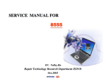
SERVICE MANUAL & TROUBLESHOOTING GUIDE FOR
7170
BY: Richard Wang
TESTING TECHNOLOGY DEPARTMENT / TSSC
JUL. 2001
7170 N/B MAINTENANCE
CONTENTS
1. Hardware Engineering Specification------------------------------------------------------------------------------- 3
Specification-------------------------------------------------------------------------------1.1
1.2
1.3
1.4
1.5
Introduction-----------------------------------------------------------------------------------------------------------------------------Hardware System----------------------------------------------------------------------------------------------------------------------System Power Management---------------------------------------------------------------------------------------------------------Firmware - System BIOS & Keyboard BIOS------------------------------------------------------------------------------------Periperal Component------------------------------------------------------------------------------------------------------------------
3
4
34
37
39
2. System Assembly & Disassembly------------------------------------------------------------------------------------ 43
Disassembly------------------------------------------------------------------------------------2.1 System View ------------------------------------------------------------------------------------------------------------------------------ 43
2.2 System Disassembly -------------------------------------------------------------------------------------------------------------------- 46
3. Definition & Location Connectors / Switches Setting ----------------------------------------------------------- 65
3.1 7170 Main Board -----------------------------------------------------------------------------------------------------------------------3.2 7170 DC Power Board ----------------------------------------------------------------------------------------------------------------3.3 7170 ESB Board ------------------------------------------------------------------------------------------------------------------------3.4 7170 Touch Pad Board -----------------------------------------------------------------------------------------------------------------
65
68
69
69
4. Definition & Location Of Major Components-------------------------------------------------------------------- 70
Components--------------------------------------------------------------------4.1 7170 Main Board ------------------------------------------------------------------------------------------------------------------------ 70
5. Pin Descriptions Of Major Components ----------------------------------------------------------------------------------------------------------------------------------------------------- 72
5.1 Pentium III/Celeron µPGA2 CPU -------------------------------------------------------------------------------------------------- 72
5.2 VIA VT8603 Twister North Bridge Controller ---------------------------------------------------------------------------------- 78
5.3 VIA VT8231 Sorth Bridge Controller --------------------------------------------------------------------------------------------- 88
1
7170 N/B MAINTENANCE
CONTENTS
6. System Block Diagram ------------------------------------------------------------------------------------------------------------------------------------------------------------------------------------------------- 100
7. Maintenance Diagnostic --------------------------------------------------------------------------------------------------------------------------------------------------------------------------------------------- 101
7.1
7.2
7.3
7.4
Introduction ----------------------------------------------------------------------------------------------------------------------------Error Codes ----------------------------------------------------------------------------------------------------------------------------Diagnostic Tools -----------------------------------------------------------------------------------------------------------------------Circuit ------------------------------------------------------------------------------------------------------------------------------------
101
102
108
108
8. Trouble Shooting --------------------------------------------------------------------------------------------------------------------------------------------------------------------------------------------------------------- 109
8.1 No Power --------------------------------------------------------------------------------------------------------------------------------8.2 No Display ------------------------------------------------------------------------------------------------------------------------------8.3 VGA Controller Failure -------------------------------------------------------------------------------------------------------------8.4 Memory Test Error -------------------------------------------------------------------------------------------------------------------8.5 Keyboard ( K/B ) , Touch-Pad ( T/P ) , ESB Test Error ----------------------------------------------------------------------8.6 CD-ROM Drive Test Error ---------------------------------------------------------------------------------------------------------8.7 Hard Drive Test Error ---------------------------------------------------------------------------------------------------------------8.8 USB Port Test Error -----------------------------------------------------------------------------------------------------------------8.9 PIO Port Test Error ------------------------------------------------------------------------------------------------------------------8.10 Audio Failure --------------------------------------------------------------------------------------------------------------------------
110
118
121
123
125
127
129
131
133
135
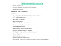
9. Spare Parts List ------------------------------------------------------------------------------------------------------------------------------------------------------------------------------------------------------------------- 137
10. System Explode View ------------------------------------------------------------------------------------------------------------------------------------------------------------------------------------------------- 146
11. Circuit Diagram --------------------------------------------------------------------------------------------------------------------------------------------------------------------------------------------------------------- 147
12. Reference ------------------------------------------------------------------------------------------------------------------------------------------------------------------------------------------------------------------------------- 175
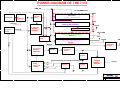
2
7170 N/B MAINTENANCE
1. Hardware Engineering Specification
1.1. Introduction
1.1.1. General Description
This document describes the system hardware engineering specification for 7170 portable notebook computer system.
The 7170NB is a excellently high performance and highly portable platform.
1.1.2. System Overview
The Architecture of 7170NB is based on PCI - ISA structure. It provides a high performance platform on PCI bus up
to 33MHz and is fully compatible with IBM PC/AT specification which have standard hardware peripheral interface and
supports AGP 4X(133MHz). 7170NB adopts Intel Celeron 128K integrated level 2 cache in a FC-PGA package which have
an excellent ability of code execution for multimedia applications operating at 700/733/766 and 800MHz & Intel Pentium Ⅲ
CPU , 256K integrated level 2 cache in a FC-PGA package which have an excellent ability of code execution for multimedia
applications operating at 800/866/933/1G and 1.33GHz
The power management complies with Advanced Configuration and Power Interface (ACPI) 1.0. It also provides easy
configuration through CMOS ROM setup which is built in system BIOS software and can be pop-up by pressing F2 at
system start up or warm reset. System also provides LEDs to display system status, such as HDD, FDD, CD-ROM, NUM
LOCK, CAP LOCK, SCROLL LOCK, AC Power indicator and battery present, capacity & charging, email/Blue-tooth status
7170NB system is equipped with one 2.5”, hard disk drive(supports Ultra DMA33/66), one 5 1/4" 24x CD-ROM
drive(DVD optional), one USB floppy, one 56kbps Fax/Modem, one 10/100 Mb LAN, one PCMCIA sockets, internal
keyboard, Touch pad with scroll-up/down buttons, two stereo speakers, TFT LCD panel, one FIR, PIO/TV-OUT, one VGA
connector for CRT and one PS/2 port for external keyboard or mouse. System also provides in-system flash ROM
programming for easy future upgrade.
A full set of software drivers and utilities are available to allow advanced operating system such as Windows 98 ,
Windows 98SE ,Window NT ,Window2000, Windows ME and Windows XP to take full advantages of the hardware
capabilities. Features such as bus mastering IDE, Windows 98-ready Plug & Play, Advanced Power Management (APM)
with application restart, software-controlled power shutdown.
Following chapters will describe more detail for each individual sub-systems and functions.
3
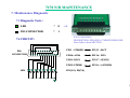
7170 N/B MAINTENANCE
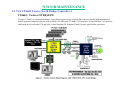
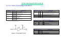
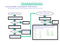
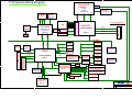
1 .2 . H a rd w a r e S y stem
1 .2 .1 S y ste m b lo c k
USB
CRT
Int. MIC
2/1
Mini
MODEM 1394
PS2
PRINTER
TV-OUT ACIN
FIR
POWER
FAN
CPU
ON/OFF
Q-KEY BOARD
LAN
PCMCIA
D/D BOARD
CDROM
SODIMMx2
T-PAD
HDD
MDC
MINI-PCI
SPKR
BATTERY
LEDs
EMAIL/
Blue-
MIC
L-IN
L-OUT VOLUME
LID
SPKR
Tooth
T-PAD BOARD
4
7170 N/B MAINTENANCE
1.2.2 System parts
CPU : Intel Celeron (700/733/766/800MHz) with FC-PGA package OR
Intel Pentium Ⅲ (800EB/866/933/1000/1133MHz) with FC-PGA package
Space reserve for VIA CyrixIII
CORE LOGIC :
VIA VT8603 (North Bridge : 66/100/133 SOCKET 370 CPU
Integrated S3 Savage4 AGP4X Graphics Core with LVDS Interface
Memory Controller Supporting PC100/PC133 SDRAM
VIA VT8231(South Bridge) : PC99 Compliant PCI to ISA Bridge
Integrated Super-IO (LPT, COM)
Integrate Fast Ethernet
AC97 Audio, USB, RTC
UltraDMA-33/66 Master Mode PCI-EIDE Controller for HDD,
DROM/DVD
ACPI, EPM, SMBus, Temperature Monitor
PCMCIA Controller : TI PC4410(PCMCIA) + TPS2211(Power Switch)
1394 Controller : TI PC4410(MAC) + TSB41AB1(PHY)
FIR Controller : NS 97338VJG
Embedded Controller : Hitachi H8/3437S
Audio System : Codec RealTek ALC200 (or Crystal CS4299) PQFP + Amp. TI TPA0202
FIR Module : HP HSDL-3600#007 IR module
5
7170 N/B MAINTENANCE
Thermal Sensor : AD1021 (or Genesys Logic GL528SM)
Memory System : Two 144 pin SO-DIMM (PC100/PC133 64/128/256MB)
Flash Memory (BIOS) :
28F020(2M bit)
56.6K FAX/MODEM RJ11 : 30 pin MDC board
LAN RJ45 : VT8231(MAC) + LSI80227(PHY)
Mini PCI : Wireless LAN/ Modem
Other Function : Reserve Blue Tooth function
6
7170 N/B MAINTENANCE
1.2.3 CPU
Intel Celeron Processor for the FC-PGA370 socket
Available at 800/ 766/ 733/ 700/ 733/ 700/ 667/ 633/ 600/ 566 /533 /533/ 500/ 466/ 433/ 400/ 366/ 333
/ 300 MHz core frequencies with 128KB level-two cache (on die). (300/ 266 MHz core frequencies
without level-two cache).
Intel’s latest Celeron processors in the FC_PGA package are manufactured using the advanced 0.18
micron technology.
Binary compatible with applications running on previous members of the Intel microprocessor line.
Dynamic execution microarchitecture.
Operates on a 66MHz, transaction-oriented system bus.
Specifically designed for uni-processor based Value PC systems, with the capabilities of MMX
technology.
Power Management capabilities.
Optimized for 32-bit applications running on advanced 32-bit operating systems.
Integrated high performance 32KB instruction and data, nonblocking, level-one cache : separate 16KB
instruction and 16KB data caches.
Integrated thermal diode.
7
7170 N/B MAINTENANCE
Pentium Ⅲ Processor for the FC-PGA370 socket
Available in 1.133G/ 1.0G/ 933/ 866/ 800EB/ 733/ 667,600EB/ 533EB MHz for 133 MHz system
bus.
Available in 850/ 800/ 750/ 700/ 650/ 600E/ 550E and 550E MHz for 100 MHz system bus.
System bus frequency at 100 MHz and 133 MHz(“E” denotes support for Advanced Transfer Cache
and Advanced system buffering ;”B” denotes support for a 133MHz System bus where both bus
frequencies are available for order per each given core
Available in versions that incorporate 256KB Advanced Transfer Cache(on-die, full speed Level 2(L2)
cache with Error Correcting Code(ECC))
Dual Independent Bus (DIB) architecture:
Separate dedicated external System Bus and dedicated internal high-speed Cache bus.
Internet Streaming SIMD Extensions for enhanced video ,sound and 3D performance
Binary compatible with applications running on previous members of the Intel microprocessor line.
Dynamic execution micro architecture.
Intel Processor Serial Number.
Power Management capabilities
System Management mode
Multiple low-power states.
Optimized for 32-bit applications running on advanced 32-bit operating system.
8
7170 N/B MAINTENANCE
Flip Chip pin Grid Array (FC-PGA) packaging technology ;FC-PGA processors deliver high
performance with improved handling protection and socketability.
Integrated high performance 16KB instruction and 16KB data, nonblocking, level one cache.
256 KB Integrated Full Speed level two cache allows for low latency on read/store operations.
Double Quad Word Wide (256bit) cache data bus provides extremely high throughput on read/store
operations.
8-way cache associativity provides improved cache hit rate on reads/store operations.
Error-correcting code for Systen Bus data.
Enables systems which are scaleable for up to two processor.
9
7170 N/B MAINTENANCE
1.2.4 Core Logic Controller :
1.2.4.1 VIA Twister VT8603 (with Mobile VGA Savage4)
CPU Interface
Socket 370 support for Intel Pentium III, Pentium II, and Celeron processors
66/100/133 MHz CPU FrontSide Bus (FSB)
Built-in Phase Lock Loop circuitry for optimal skew control within and between clocking regions
Five outstanding transactions (four In-Order Queue (IOQ) plus one output latch)
Dynamic deferred transaction support
Advanced High-Performance DRAM Controller
DRAM interface runs synchronous (66/66, 100/100, 133/133) mode or pseudo
-synchronous (66/100, 100/66,
100/133,133/100) mode with FSB
Concurrent CPU, AGP, and PCI access
Supports SDRAM and VCM SDRAM memory types
Support 3 DIMMs or 6 banks for up to 1.5 GB of DRAM (256Mb DRAM technology)
64-bit data width
Supports maximum 8-bank interleave (8 pages open simultaneously); banks are allocated based on LRU
SDRAM X-1-1-1-1-1-1-1 back-to-back accesses
10
7170 N/B MAINTENANCE
Integrated Savage4 2D/3D/Video Accelerator
– Optimized Shared Memory Architecture (SMA)
– 8 to 32 MB frame buffer using system memory
– Floating point triangle setup engine
– Single cycle 128-bit 3D architecture
– 8M triangles/second setup engine
– 140M pixels/second trilinear fill rate
– Full internal AGP 4x performance
– S3 DX7 texture compression (S3TCÔ)
– Next generation, 128-bit 2D graphics engine
– High quality DVD video playback
– Flat panel monitor support
– 2D/3D resolutions up to 1920x1440
3D Rendering Features
– Single-pass multiple textures
– Anisotropic filtering
– 8-bit stencil buffer
– 32-bit true color rendering
– Specular lighting and diffuse shading
– Alpha blending modes
11
7170 N/B MAINTENANCE
– Massive 2K x 2K textures
– MPEG-2 video textures
– Vertex and table fog
– 16 or 24-bit Z-buffering
– Sprite anti-aliasing, reflection mapping, texture morphing, shadows, procedural textures and atmospheric effects
2D Hardware Acceleration Features
– ROP3 Ternary Raster Operation BitBLTs
– 8, 16, and 32 bpp mode acceleration
Motion Video Architecture
– High quality up/down scaler
– Planar to packed format conversion
– Motion compensation for full speed DVD playback
– Hardware subpicture blending and highlights
– Multiple video windows for video conferencing
– Contrast, hue, saturation, brightness and gamma controls
– Digital port for NTSC/PAL TV encoders
12
7170 N/B MAINTENANCE
Extensive LCD Support
– 36-bit DSTN/TFT flat panel interface with 256 gray shade support
– Integrated 2-channel 110 MHz LVDS interface
– Support for all resolutions up to 1280x1024
– ZV-Port Interface
– Panel power sequencing
– Hardware Suspend/Standby control
Flat Panel Monitor Support
– 12-bit TFT flat panel interface to TMDS encoders
– Digital Visual Interface (DVI) 1.0 compliant
Concurrent PCI Bus Controller
– PCI 2.2 compliant, 32-bit 3.3V PCI interface with 5V tolerant inputs
– Supports up to 5 PCI masters
– PCI to system memory data streaming support
– Delay transaction from PCI master accessing DRAM
– Symmetric arbitration between Host/PCI bus for optimized system performance
13
7170 N/B MAINTENANCE
Advanced System Power Management Support
– Dynamic power down of SDRAM (CKE)
– Independent clock stop controls for CPU / SDRAM, AGP, and PCI bus
– PCI and AGP bus clock run and clock generator control
– VTT suspend power plane preserves memory data
– Suspend-to-DRAM and self-refresh power down
– Low-leakage I/O pads
– ACPI 1.0 and PCI Bus Power Management 1.1 compliant
Full Software Support
– Drivers for major operating systems and APIs: [Windows 9x, Windows NT 4.0, Windows 2000, Direct3D,
DirectDraw and DirectShow, OpenGL ICD for Windows 9x, NT, and 2000]
– North Bridge/Chipset and Video BIOS support
Additional Features
– 250 MHz RAMDAC with Gamma Correction
– 12-bit interface to external TV encoder
– I 2 C Serial Bus and DDC Monitor Communications
– 2.5V Core and Mixed 3.3V/5V Tolerant and GTL+ I/O
35 x 35mm PBGA package with 552 balls
14
7170 N/B MAINTENANCE
1.2.4.2 South Bridge VIA VT8231
Inter-operable with VIA and other Host-to-PCI Bridges
– Combine with VT82C694X for a complete 66 / 100 / 133 MHz Socket370 AGP 4x system (Apollo
Pro133A)
– Combine with VT8601 for a complete 66 / 100 / 133 MHz Socket370 system with integrated 2D/3D
graphics (Apollo ProMedia)
– Inter-operable with Intel or other Host-to-PCI bridges for a complete PC99 compliant PCI/AGP system
Integrated Peripheral Controllers
– Integrated Fast Ethernet Controller with 1 / 10 / 100 Mbit capability
– Integrated USB Controller with two root hub and four function ports
– Dual channel UltraDMA-33 / 66 master mode EIDE controller
– AC-link interface for AC-97 audio codec and modem codec
– HSP modem support
– Integrated SoundBlasterPro / DirectSound compatible digital audio controller
Integrated Legacy Functions
– Integrated Keyboard Controller with PS2 mouse support
– Integrated DS12885-style Real Time Clock with extended 256 byte CMOS RAM and Day/Month Alarm
for ACPI
– Integrated Bus Controller including DMA, timer, and interrupt controller
– Serial IRQ for docking and non-docking applications
15
7170 N/B MAINTENANCE
– Flash EPROM, 32Mbit (4Mbyte) EPROM and combined BIOS support
– Fast reset and Gate A20 operation
Fast Ethernet Controller
– High performance PCI master interface with scatter / gather and bursting capability
– Standard MII interface to Ethernet or HomePNA PHYceiver
– 1 / 10 / 100 MHz full and half duplex operation
– Transmit data buffer byte alignment for low CPU utilization
– Separate 2K byte FIFOs for receive and transmit of full Ethernet packets
– Flexible dynamically loadable EEPROM algorithm
– Physical, Broadcast, and Multicast address filtering using hashing function
– Flexible wakeup events: link status change, magic packet, unicast physical address match, predefined pattern
match
– Software controllable power down
UltraDMA-33 / 66 / 100 Master Mode PCI EIDE Controller
– Dual channel master mode PCI supporting four Enhanced IDE devices
– Transfer rate up to 100MB/sec to cover up to PIO mode 4, multi-word DMA mode 2, and UltraDMA mode 5
– Thirty-two levels (doublewords) of prefetch and write buffers per channel
– Dual DMA engine for concurrent dual channel operation
– Bus master programming interface for SFF-8038i rev.1.0 and Windows-95 / 98 / 2000 compliant
– Full scatter gather capability
16
7170 N/B MAINTENANCE
– Support ATAPI compliant devices including DVD devices
– Support PCI native and ATA compatibility modes
– Complete software driver support
Integrated Super IO Controller
– Supports IR port, parallel port, and floppy disk controller functions
– Serial Port Programmable character lengths (5,6,7,8)
Even, odd, stick or no parity bit generation and detection
Programmable baud rate generator
Independent transmit/receiver FIFOs Modem Control
Plug and play with 96 base IO address and 12 IRQ options
– Fast IR (FIR) port
IrDA 1.0 SIR and IrDA 1.1 FIR compliant
IR function through the second serial port
Infrared-IrDA (HPSIR) and ASK (Amplitude Shift Keyed) IR
– Multi-mode parallel port
Standard mode, ECP and EPP support
Dynamic and static switch between parallel port pinout and FDC pinout
Plug and play with 192 base IO address, 12 IRQ and 4 DMA options
– Floppy Disk Controller
16 bytes of FIFO
Data rates up to 1Mbps
Perpendicular recording driver support
Two FDDs with drive swap support
Plug and play with 48 base IO address, 12 IRQ and 4 DMA options
17
7170 N/B MAINTENANCE
SoundBlaster Pro Hardware and Direct Sound Ready AC97 Digital Audio Controller
– Dual full-duplex Direct Sound channels between system memory and AC97 link
– PCI master interface with scatter / gather and bursting capability
– 32 byte FIFO of each direct sound channel
– Host based sample rate converter and mixer
– Standard v1.0 or v2.0 AC97 Codec interface for single or cascaded AC97 Codec’s from multiple vendors
– Loopback capability for re-directing mixed audio streams into USB and 1394 speakers
– Hardware SoundBlaster Pro for Windows DOS box and real-mode DOS legacy compatibility
– Plug and play with 4 IRQ, 4 DMA, and 4 I/O space options for SoundBlaster Pro and MIDI hardware
– Hardware assisted FM synthesis for legacy compatibility
– Direct two game ports and one MIDI port interface
– Complete software driver support for Windows-95/98/2000 and Windows-NT
MC97 HSP Modem Controller
– PCI bus master interface with scatter / gather and burst capability
– Standard AC97 codec interface for MC or AMC codec
– Wake on ring in APM or ACPI mode through AC97 link
– Supported by most HSP modem vendors
18
7170 N/B MAINTENANCE
Universal Serial Bus Controller
– USB v.1.1 and Intel Universal HCI v.1.1 compatible
– Eighteen level (doublewords) data FIFO with full scatter and gather capability
– Root hub and four function ports
– Integrated physical layer transceivers with optional over-current detection status on USB inputs
– Legacy keyboard and PS/2 mouse support
System Management Bus Interface
– One master / slave SMBus and one slave-only SMBus
– Host interface for processor communications
– Slave interface for external SMBus masters
Voltage, Temperature, Fan Speed Monitor and Controller
– Five universal input channels for voltage or temperature sensing
– Two fan-speed monitoring channels
– Input channel for thermal diode in Intel™ high speed Pentium II™ / Pentium III™ CPUs
– Programmable control, status, monitor and alarm for flexible desktop management
– External thermister or internal bandgap temperature sensing
– Automatic clock throttling with integrated temperature sensing
– Internal core VCC voltage sensing
– Flexible external voltage sensing arrangement (any positive supply and battery)
19
7170 N/B MAINTENANCE
Sophisticated PC99-Compatible Mobile Power Management
– Supports both ACPI (Advanced Configuration and Power Interface) and legacy (APM) power management
– ACPI v1.0 Compliant
– APM v1.2 Compliant
– CPU clock throttling and clock stop control for complete ACPI C0 to C3 state support
– PCI bus clock run, Power Management Enable (PME) control, and PCI/CPU clock generator stop control
– Supports multiple system suspend types: power-on suspends with flexible CPU/PCI bus reset options,
suspend to DRAM, and suspend to disk (soft-off), all with hardware automatic wake-up
– Multiple suspend power plane controls and suspend status indicators
– One idle timer, one peripheral timer and one general purpose timer, plus 24/32-bit ACPI compliant timer
– Normal, doze, sleep, suspend and conserve modes
– Global and local device power control
– System event monitoring with two event classes
– Primary and secondary interrupt differentiation for individual channels
– Dedicated input pins for power and sleep buttons, external modem ring indicator, and notebook lid open/close
for system wake-up
– Multiple internal and external SMI sources for flexible power management models
– One programmable chip select and one microcontroller chip select
– Enhanced integrated real time clock (RTC) with date alarm, month alarm, and century field
– Thermal alarm on either external or any combination of three internal temperature sensing circuits
20
7170 N/B MAINTENANCE
– Hot docking support
– I/O pad leakage control
Plug and Play Controller
– PCI interrupts steerable to any interrupt channel
– Steerable interrupts for integrated peripheral controllers: USB, floppy, serial, parallel, audio, soundblaster, MIDI
– Steerable DMA channels for integrated parallel, and soundblaster pro controllers
– One additional steerable interrupt channel for on-board plug and play devices
– Microsoft Windows 2000 TM , Windows ME TM ,Windows 98SE TM , Windows 98 TM , Windows NT TM ,
Windows 95 TM and plug and play
BIOS compliant
Built-in NAND-tree pin scan test capability
0.30um, 3.3V, low power CMOS process
Single chip 27x27 mm, 376 pin BGA
21
7170 N/B MAINTENANCE
1.2.5 PCMCIA/1394 Link Controller: PCI4410
The PCI4410 supports the following features:
- A 209-ball MicroStar Ball Grid Array (GHK) package
- 3.3-V core logic with universal PCI interfaces compatible with 3.3-V and 5-V PCI signaling environments
- Mix-and-match 5-V/3.3-V 16-bit PC Cards and 3.3-V CardBus Cards
- Single PC Card or CardBus slot with hot insertion and removal
- Burst transfers to maximize data throughput on the PCI bus and the CardBus bus
- Parallel PCI interrupts, parallel ISA IRQ and parallel PCI interrupts, serial ISA IRQ with parallel PCI
interrupts, and serial ISA IRQ and PCI interrupts
- Serial EEPROM interface for loading subsystem ID and subsystem vendor ID
- Pipelined architecture allows greater than 130M bps sustained throughput from CardBus-to-PCI and
fromPCI-to-CardBus
- Interface to parallel single-slot PC Card power interface switches like the TI TPS2211
- Up to five general-purpose I/Os
- Five PCI memory windows and two I/O windows available to the 16-bit PC Card socket
- Two I/O windows and two memory windows available to the CardBus socket
- Exchangeable Card Architecture (ExCA) compatible registers are mapped in memory and I/O space
- Intel 82365SL-DF and 82365SL register compatible
- Distributed DMA (DDMA) and PC/PCI DMA
- 6-Bit DMA on the PC Card socket
22
7170 N/B MAINTENANCE
- PCI Bus Lock (LOCK)
- Advanced Submicron, Low-Power CMOS Technology
- Internal Ring Oscillator
1.2.6 LAN PHY: LSI80227
features:
- Single Chip 100Base-TX / FX/10Base-T Physical Layer Solution
- 3.3V Version of SEEQ 80221
- Dual Speed - 10/100 Mbps
- Half And Full Duplex
- MII Interface To Ethernet Controller
- MI Interface For Configuration & Status
- Optional Repeater Interface
- AutoNegotiation: 10/100, Full/Half Duplex
- Meets All Applicable IEEE 802.3 Standards
- On Chip Wave Shaping - No External Filters Required
- Adaptive Equalizer
- Baseline Wander Correction
- Interface to External 100Base-T4 PHY
- LED Outputs: Link/Activity/ Collision/ Full Duplex/ 10/100/ User Programmable
23
7170 N/B MAINTENANCE
- Many User Features And Options
- Few External Components
- 3.3V Supply with 5V Tolerant I/O
- 64L TQFP
1.2.7 Embedded Controller : Hitachi H8/3437S
CPU
- Two-way general register configuration
Eight 16-bit registers or Sixteen 8-bit registers
- High-speed operation
Maximum clock rate : 16Mhz at 5V
Memory
- Include 32KB ROM and 1KB RAM
16-bit free-running timer
- One 16-bit free-running counter
- Two output-compare lines
- Four input capture lines
8-bit timer ( 2 channels )
- Each channel has one 8-bit up-counter , two time constant registers
PWM timer (2 channels)
- Resolution :1/250
- Duty cycle can be set from 0 to 100%
24
7170 N/B MAINTENANCE
I2C bus interface ( one channel )
- Include single master mode and slave mode
Host interface ( HIF)
- 8-bit host interface port
- Three host interrupt requests ( HIRQ1,11,12)
- Regular and fast A20 gate output
Keyboard controller
- Controls a matrix-scan keyboard by providing a keyboard scan function with wake-up interrupts
- And sense ports
A/D converter
- 10-bit resolution
- 8 channels : single or scan mode (selectable )
D/A converter
- 8-bit resolution
- 2 channels
Interrupts
- Nine external interrupt lines : NMI# , IRQ0 to 7#
- 26 on-chip interrupt sources
Power-down modes
- Sleep mode
- Software standby mode
- Hardware standby mode
25
7170 N/B MAINTENANCE
A single chip microcomputer
On-chip flash memory
Maximum 64-kbyte address space
Support three PS/2 port for external keyboard ,mouse and internal track pad.
Support SMI,SCI trigger input:
Cover switch
Battery charging control
Smart Battery monitoring
Control D/D system on/off
Fan control and LED indicator serial interface
100pin TQFP
26
7170 N/B MAINTENANCE
1.2.8 Audio System
1.2.8.1 AC97 CODEC : ALC200 (or CS4299) -PQFP
AC ’97 2.1 Compatible
Industry Leading Mixed Signal Technology
20-bit Stereo Digital-to-Analog Converter and 18-bit Ste-reo Analog to Digital Converter with Sample
Rate Conversion
Four Analog Line-level Stereo Inputs for Connection from LINE IN, CD, VIDEO, and AUX
Two Analog Line-level Mono Inputs for Modem Sub-system and Internal PC Beeper
Mono Microphone Input Switchable from Two External Sources
High Quality Differential CD Input
Dual Stereo Line-level Outputs
Extensive Power Management Support
Meets or Exceeds Microsoft’s ® PC 98 and PC 99 Audio Performance Requirements
3D Stereo Enhancement
Sample Rate Converters
27
7170 N/B MAINTENANCE
combined with driver software and an AC’97 CODEC provides a complete high quality
audio solution,
Feature Include:
- MPU-401 interface
- FM synthesizer
- Game Port (disable in 7170 NB system)
- MIDI port. (disable in 7170 NB system)
- MODEM
- CD-ROM
- User-Defined GPIO
- Volume Control: Rotary VR
- Stereo BTL 2x1 W Amplifiers(TPA0202) With 8 Ohm Load.
- 16 Bit Stereo ADC & DAC For Record And Play Back
- Programmable Sample Rates From 4kHz To 44.1kHz For Record And Playback
- Microphone in * 1 (3.5 mm phone-jack)
- Headphone out * 1: stereo (3.5mm phone-jack) (disable in 7170 NB system)
- Built-in Speaker * 2 (1w, 8 ohm)
- Built-in Microphone * 1
28
7170 N/B MAINTENANCE
1.2.9 IR Module : HSDL-3600#007
Fully Compliant to IrDA 1.1 Specifications
- 115.2 kb/s to 4 Mb/s operation
- excellent nose-to-nose operation
Compatible with ASK, HP-SIR
IEC825-Class 1 Eye Safe
Wide Operating Voltage Range
- 2.7 V to 5.25 V
Small Module Size
- 4.0 x 12.2 x 5.1 mm (HxWxD)
Complete Shutdown
- TXD, RXD, PIN diode
Low Shutdown Current
- 10 nA typical
Adjustable Optical Power Management
- Adjustable LED drive-current to maintain link integrity
Single Rx Data Output
- FIR Select pin switch to FIR
Integrated EMI Shield
- Excellent noise immunity
Edge Detection Input
- Prevents the LED from long turn-on time
Interface to various Super I/O and Controller Devices
Designed to Accommodate Light Loss with Cosmetic Window
29
7170 N/B MAINTENANCE
1.2.10 Memory System
1.2.12.2 Main memory
SO-DIMM
- Two SO-DIMM sockets on Mother Board for expansion
- Supports JEDEC specification : 144 SO-DIMM socket
- Supports 3.3V PC100/PC133 SDRAM DIMM
- 2 banks on each socket
The memory subsystem supports two 3.3V 144-pin SO-DIMM sockets for totally up to 512MB of Main memory.
Here are some main memory system essential characteristics:
144-pin SO DIMM socket
2
Memory Voltage
3.3V ± 10%
Memory Module Type
64MB/128MB/256MB
Banks on DIMM
4
Bank Ordering
Auto ordering by BIOS
Memory type selection
Auto-detect by BIOS
Mixed type DRAM support
Yes
30
7170 N/B MAINTENANCE
1.2.11 Mass Storage Sub-system
7170NB system is an two spindles NB. There are one removable 2.5" hard disk drive and 24X CD-ROM or
DVD or CDRW installed in it. This IDE interface is compliant with ATA specification and UltraDMA 33/66MB.
1.2.12 I/O Interface
- One standard parallel port with Output only/Bi-direction/ECP/EPP functions
- One serial ports, for FIR/MIR/SIR/SHARP ASK
COM port assignment COM2: IR / RS-232 / Disable
- One external CRT connector for CRT display
- One PS/2 interface for external KB, mouse or other PS2 devices
- One CARDBUS sockets support type II.
- Two USB V1.1 connector
- One DC Jack for Adapt in
- One MODEM RJ-11 phone jack for PSTN line and one RJ-45 for 10/100 base LAN.
- Dual stereo line level speaker outputs
- Microphone input and one internal microphone.
- Tunable volume by variable resistor
- One Mini-PCI socket support Type IIIA.
31
7170 N/B MAINTENANCE
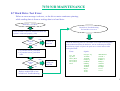
1.2.13 Special Feature Function2
1.2.13.1. Hot Key Function
Keys Combination
Feature
Meaning
Fn + F5
Display switch
Rotate display mode in LCD only, CRT only and
simultaneously display and TV output.
Fn + F6
Brightness down
Decreases the LCD brightness
Fn + F7
Brightness up
Increase the LCD brightness
Fn + F8
Contrast down
Decrease the LCD contrast
Fn + F9
Contrast up
Increase the LCD contrast
Fn + F10
Enable/Disable battery Toggle battery low beep warming on/off
warming beep
Fn + F11
Panel on/off
Fn + F12
Suspend to Dram/HDD Force the computer into either suspend to HDD or
suspend to DRAM mode depending on BIOS setup
Toggle Display ( panel , CRT,TV ) On/Off
1.2.13.2. Flash ROM (BIOS)
7170 NB system utilizes the state-of-the-art Flash EEPROM technology. User can upgrade the system BIOS in
the future just running the program from MiTAC.
32
7170 N/B MAINTENANCE
1.2.13.3. LED Indicators
System has nine status LED indicators to display system activity which include below LCD panel unit and above
keyboard:
1. Three LED indicators below LCD panel unit:
From left to right that indicate AC POWER, BATTERY POWER and BATTERY STATUS
• AC POWER: This LED lights green when the notebook is being powered by AC, and flash (on 1 second, off
1 second ) when Suspend to DRAM is active using AC power. The LED is off when the notebook is off or
powered by batteries, or when Suspend to Disk.
• BATTERY POWER: This LED lights green when the notebook is being powered by batteries, and flashes
(on 1 second, off 1 second ) when Suspend to DRAM is active using battery power. The LED is off when the
notebook is off or powered by AC, or when Suspend to Disk.
• BATTERY STATUS : During normal operation, this LED stays off as long as the battery is charged. When
the battery charge drops to 10% of capacity, the LED lights red, flashes per 1 second and beeps per 2 second.
When AC is connected, this indicator glows green if the battery pack is fully charged, or orange (amber) if the
battery is being charged.
• Five LED indicators in front of palm rest:
From left to right that indicates CD-ROM/MO, HARD DISK DRIVE, , NUM LOCK, CAPS LOCK and
SCROLL LOCK.
• Email/ Blue-Tooth LED indicators in front of palm rest:
The left side green LED flashing means new mail coming. Otherwise the LED is always OFF. The right side
red LED ON means Blue-Tooth module turn ON.
33
7170 N/B MAINTENANCE
1.3 System Power Management
1.3.1 System Management Mode
7170NB system has built in several power saving modes to prolong the battery usage for mobile purpose. User can
enable and configure different degrees of power management modes via ROM CMOS setup ( booting by pressing F2
key). Following are the descriptions of the SMM and power management modes supported.
1.3.1.1. Full-On Mode
In this mode, each device is running with the maximal speed. CPU clock is up to its maximum.
1.3.1.2. Doze Mode
In this mode, CPU will be toggling between on & stop grant mode either. The technology will be clock throttling.
This can save battery power without loosing much computing capability.
The CPU power consumption and temperature is lowered in this mode.
1.3.1.3. Standby Mode
For more power saving, it turns of f the peripheral component. In this mode, the following is the status of each
device.
- CPU : stop grant
- VGA: software suspend
- LCD : backlight off
- HDD: spin down
- FDD : standby
- FDD : standby
34
7170 N/B MAINTENANCE
1.3.1.4. Suspend Mode
The most chipsets of the system is entering power down mode for more power saving.
Suspend to RAM :
CPU: off
N.B: off
S.B: partial off
VGA: Suspend
PCMCIA: Standby
Audio: off
Suspend to HDD :
All devices are stopped clock and power-off, only EC is lived if battery or ac still plug in .At this time ,
system status is saved in HDD. All system status will be restored when toggle power button system powered on
again.
1.3.1.5. Other Power Management Functions
1.3.1.5.1. HDD & Video access
System has the ability to monitor video and hard disk activity. User can enable monitoring function for video
and/or hard disk individually. When there is no video and/or hard disk activity, system will enter next PMU
state depending on the application. When the VGA activity monitoring is enabled, the performance of the
system will have some impact.
1.3.1.5.2. Cover Switch
System automatically provides power saving on monitoring Cover Switch. It will save battery power and prolong
the usage time when user closes the notebook cover . There are three functions to be chosen.
35
7170 N/B MAINTENANCE
1.3.2 Other Power Management Functions
1.3.2.1. HDD & Video access
System has the ability to monitor video and hard disk activity. User can enable monitoring function for video
and/or hard disk individually. When there is no video and/or hard disk activity, system will enter next PMU
state depending on the application. When the VGA activity monitoring is enabled, the performance of the
system will have some impact.
1.3.2.2. Cover Switch
System automatically provides power saving on monitoring Cover Switch. It will save battery power and prolong
the usage time when user closes the notebook cover . There are three functions to be chosen.
1. Switch to CRT
2. Panel Off
3. Suspend --- Depend on BIOS setting ( STR or STD)
1.3.2.3. Battery Warning
System also provides battery capacity monitoring and gives user a warning so that users have chance to save
their data before battery dead. Also , this function protects system from mal-function while battery capacity is low.
1.3.2.4. Battery Warning State
7170 NB system provides battery management function and gives warning while battery is in It’s low power
state. When the battery capacity is below 9% (Battery Warning State), system will generate beep for every 4
seconds (System beeps only if BIOS setup enable Battery Warning Beeping). When hearing the beeping, it is
recommended that user should plug in AC adapter to get power from external source, or stop working and
save his data file to prevent disastrous results.
1.3.2.5. Battery Dead State
W hen the battery voltage level reach 11 volts, system will shut down automatically in order to extend the
battery packs' life.
36
7170 N/B MAINTENANCE
1.3.3. Fan Power on/off Management
The fan is always on except suspend power off to cool the CPU temperature down.
1.4 Firmware - System BIOS & Keyboard BIOS
7170NB use Phoenix BIOS as the system firmware and keyboard firmware .For further detail information regarding
the firmware , please refer to 7170NB software document.
(refer software engineer spec)
1.4.1 SYSTEM RESOURCE
1.4.1.1 PCI INT MAP
INT
DEVICE
INTA
CARDBUS
INTB
(VGA in North Bridge)
INTC
MINI PCI
INTD
USB/ MINI PCI(REV)
1394/ LAN
37
7170 N/B MAINTENANCE
1.4.1.2 PCI BUS MASTER REQUEST
REQ
DEVICE
REQ0
CARDBUS
REQ1
No Used
REQ2
VGA (in North Bridge)
REQ3
MINI PCI
REQ4
LAN
1.4.1.3 IDSEL
AD BUS
DEVICE
AD11
VGA (in North Bridge)
AD17
MINI PCI
AD21
CARDBUS
AD28
South Bridge
AD29
LAN
38
7170 N/B MAINTENANCE
1.5 Peripheral Component
1.5.1 LCD
UNIPAC
UB133X01-2
TFT XGA
- pixels : 1024(H) By 768(V)
- screen size : 13.3inch
- colors : 262k(3x6 bit)
- interface : LVDS single cannel
- lump : CCFL
- D/C for panel : 3.3V
- Power Consumption : 3.66W(typ)
- Weight : 500g (typ)
- Lamp starting voltage : 925 Vrms (typ)
1.5.2 Internal Keyboard
IBM 106 key compatible keyboard layout
Key pitch : 19mm
Length : 300mm
Thickness : 5.3mm
Keycap pull off force : >= 800g
MAX. keytop depressing force :
~To withstand 5 Kgf at the center of keytop for 1 minute.
39
7170 N/B MAINTENANCE
Keytop Strength :
~To withstand 1Kgf at X and Y directions for 5 sec.
Power Requirement :
~The keyswitch shall require DC 6V at 0.3 mA maximum.
Contact Resistance :
~ The contact resistance is 500 ohm maximum at 200g force.
Operating Temperature : -10 to 60 degree C
High Temperature Storage : 65 degree C.
Window95 applied
1.5.3 Floppy Disk Drive
- Please use external USB Floppy Disk Device.
1.5.4 Touch Pad
Synaptics (4 buttons):
- Model TM41P-350
- Vcc : 5V +- 0.5
- Icc(max) : 4 mA
- Interface : PS/2
- X/Y position resolution : 1000 points/inch
- Dimension : 65mm x 49mm x 4.6mm
40
7170 N/B MAINTENANCE
- Effective area : 60mm x 44 mm
- Operating Temp. : 0 - 60 degree C
- Storage Humidity : 5 - 95 %,
- Storage Temp. : -40 - + 65 degree C
- ESD : 15KV applied to front surface
1.5.5 CD-ROM or DVD-ROM or CD-RW Drive
- Disk speed: X24/higher speed CD-ROM or X8 speed DVD-ROM or CD-RW.
- Host interface: IDE/ATAPI
- Ejection: Manual eject using the eject button/Automatically eject using the tray
1.5.6 HDD
- Support Ultra DMA
- 2.5” , 8.45/9.5 mm height
- Formatted Storage Capacity 10/20 GB
1.5.7 LED Indicators
Upper LEDs on D/D board
- AC. POWER, BATTERY POWER, CHARGER STATUS,
Lower LEDs on M/B board
- HARD DISK DRIVE, CD-ROM, NUM LOCK, CAPS LOCK, SCROLL LOCK and Emial/Blue-tooth status..
41
7170 N/B MAINTENANCE
1.5.8 IR port
- HSDL-3600#007 IR Module
- Meet IrDA Physical Layer Specification
- 1 cm to 1 Meter Operating Distance
- 30 degree Viewing Angle (± 15 degree )
- Support Two Channels - 2.4 Kb/s to 115.2Kb/s and 1.15Mb/s to 4.0 Mb/s
1.5.9 CMOS Battery
- VARTA CR2032 non-chargeable lithium battery
- Put in battery holder, can be replaced
- Nominal voltage : 3V
- Nominal capacity : 65mAh
- Recommended continuous Drain : 0.2 mA
- Recommended Pulse Drain : 12 mA
- Weight : 3.2 g
42
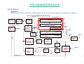
7170 N/B MAINTENANCE
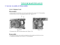
2. System Assembly & Disassembly
2.1 System View
2.1.1 Front View
Stereo Speaker Set
Device Indicators
Mail-Received Button/Indicator
Microphone Connector
Audio Input Connector
Audio Output Connector
Volume Control
Top Cover Latch
2.1.2 Left-Side View
Kensington Lock
Ventilation Openings
RJ-45 Connector
PC Card Slot
Hard Disk Drive
43
7170 N/B MAINTENANCE
2. System Assembly & Disassembly
2.1.3 Right-Side View
Battery Pack
CD-ROM/DVD-ROM Drive
IR Port
2.1.4 Rear View
Power Connector
S-Video Output Connector
Parallel Port
PS/2 Port
IEEE 1394 Port
RJ-11 Connector
USB Ports
VGA Port
Ventilation Openings
44
7170 N/B MAINTENANCE
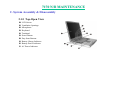
2. System Assembly & Disassembly
2.1.5 Top-Open View
LCD Screen
Ventilation Openings
Microphone
Keyboard
Touchpad
Power Button
Easy Start Buttons
Battery Charge Indicator
Battery Power Indicator
AC Power Indicator
45
7170 N/B MAINTENANCE
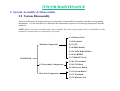
2. System Assembly & Disassembly
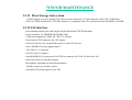
2.2 System Disassembly
The section discusses at length each major component for disassembly/reassembly and show corresponding
illustrations. Use the chart below to determine the disassembly sequence for removing components from the
notebook.
NOTE: Before you start to install/replace these modules, disconnect all peripheral devices and make sure the
notebook is not turned on or connected to AC power.
2.2.1 Battery Pack
2.2.2 Keyboard
Modular Components
2.2.3 CPU
2.2.4 HDD Module
2.2.5 CD/DVD-ROM Drive
2.2.6 SO-DIMM
2.2.7 Mini-PCI Card
NOTEBOOK
2.2.8 LCD Assembly
LCD Assembly Components
2.2.9 LCD Panel
2.2.10 Inverter Board
2.2.11 System Board
Base Unit Components
2.2.12 Touchpad
2.2.13 Modem Card
46
7170 N/B MAINTENANCE
2. System Assembly & Disassembly
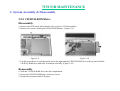
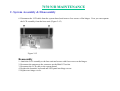
2.2.1 Battery Pack
Disassembly
1. Carefully put the notebook upside down.
2. Slide the release lever to the “unlock” ( ) position (), then slide and hold the release lever outwards and
pull the battery pack out of the compartment (). (Figure 2-1)
Figure 2-1
Reassembly
1. Push the battery pack into the compartment. The battery pack should be correctly connected
when you hear a clicking sound.
2. Slide the release lever to the “lock” ( ) position.
47
7170 N/B MAINTENANCE
2. System Assembly & Disassembly
2.2.2 Keyboard
Disassembly
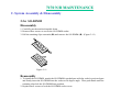
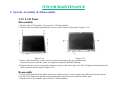
1. Open the top cover. Install a small rod, such as a straightened paper clip, into the eject hole near the power
connector of the notebook. (Figure 2-2)
Figure 2-2
Figure 2-3
2. Push the rod firmly and slide the LED panel to the left (). Then lift the LED panel up from the left side ().
(Figure 2-3)
48
7170 N/B MAINTENANCE
2. System Assembly & Disassembly
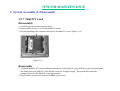
3. Slightly lift up the keyboard and disconnect the cable from the system board to detach the keyboard. (Figure 2-4)
Figure 2-4
Reassembly
1. Reconnect the keyboard cable and fit the keyboard back into place.
2. Replace the LED panel.
49
7170 N/B MAINTENANCE
2. System Assembly & Disassembly
2.2.3 CPU
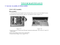
Disassembly
1. Remove the LED panel and keyboard to access the CPU compartment. (See section 2.2.2 Disassembly.)
2. Remove four screws fastening the heatsink and disconnect the fan’s power cord to free the heatsink from the CPU
module. (Figure 2-5)
•
Figure 2-5
Figure 2-6
3. Insert a minus screwdriver 101 (JIS standard) into the “OPEN” hole of the socket, and push the screwdriver
toward the CPU to free the CPU. Now you can take out the CPU from the socket. (Figure 2-6)
Reassembly
1. Align the arrowhead corner of the CPU with the beveled corner of the socket, and insert the CPU pins
into the holes. Insert the flat screwdriver into the “CLOSE” hole of the socket, and push the screwdriver
toward the CPU to secure the CPU in place.
2. Connect the fan’s power cord to the system board, fit the heatsink onto the top of the CPU
and secure with four screws.
3. Replace the keyboard and LED panel.
50
7170 N/B MAINTENANCE
2. System Assembly & Disassembly
2.2.4 HDD Module
Disassembly
1. Carefully put the notebook upside down.
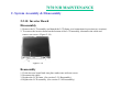
2. Remove one screw and slide the HDD module out of the compartment. (Figure 2-7)
Figure 2-7
Figure 2-8
3. Remove five screws to separate the hard disk drive from the metal shield. (Figure 2-8)
Reassembly
1. To install the hard disk drive, place it in the bracket and secure with five screws.
2. Slide the HDD module into the compartment and secure with one screw.
51
7170 N/B MAINTENANCE
2. System Assembly & Disassembly
2.2.5 CD/DVD-ROM Drive
Disassembly
1. Remove the LED panel and keyboard. (See section 2.2.2 Disassembly.)
2. Remove two screws locking the CD/DVD-ROM drive. (Figure 2-9)
Figure 2-9
Figure 2-10
3. Use the screwdriver to push the metal pad to the right and the CD/DVD-ROM drive will pop out. Hold the
CD/DVD-ROM drive and slide it outwards carefully. (Figure 2-10)
Reassembly
1. Push the CD/DVD-ROM drive into the compartment.
2. Secure the CD/DVD-ROM drive with two screws.
3. Replace the keyboard and LED panel.
52
7170 N/B MAINTENANCE
2. System Assembly & Disassembly
2.2.6 SO-DIMM
Disassembly
1. Carefully put the notebook upside down.
2. Remove three screws to access the SO-DIMM socket.
3. Pull the retaining clips outwards () and remove the SO-DIMM (). (Figure 2-11)
Figure 2-11
Reassembly
1. To install the SO-DIMM, match the SO-DIMM's notched part with the socket's projected part
and firmly insert the SO-DIMM into the socket at 20-degree angle. Then push down until the
retaining clips lock the SO-DIMM into position.
2. Replace three screws to lock the SO-DIMM socket cover.
53
7170 N/B MAINTENANCE
2. System Assembly & Disassembly
2.2.7 Mini PCI Card
Disassembly
1. Carefully put the notebook upside down.
2. Remove three screws to access the Mini PCI socket.
3. Pull the retaining clips outwards and remove the Mini PCI card. (Figure 2-12)
Figure 2-12
Reassembly
1. To install the Mini PCI card, match the notched part of the Mini PCI card with the socket's projected part
and firmly insert the Mini PCI card into the socket at 20-degree angle. Then push down until the
retaining clips lock the Mini PCI card into position.
2. Replace three screws to lock the SO-DIMM socket cover.
54
7170 N/B MAINTENANCE
2. System Assembly & Disassembly
2.2.8 LCD Assembly
Disassembly
1. Carefully put the notebook upside down and remove three screws to access the Mini PCI socket.
2. Disconnect the antenna from the connector on the Mini PCI socket. (Figure 2-13)
Figure 2-13
Figure 2-14
3. Open the top cover. Remove the LED panel, keyboard, and heatsink . (See section 2.2.2 and 2.2.3
Disassembly.)
4. Pull out the antenna from the CPU compartment.
5. Remove the two hinge covers. (Figure 2-14)
55
7170 N/B MAINTENANCE
2. System Assembly & Disassembly
6. Disconnect the LCD cable from the system board, and remove four screws of the hinges. Now you can separate
the LCD assembly from the base unit. (Figure 2-15)
Figure 2-15
Reassembly
1. Attach the LCD assembly to the base unit and secure with four screws on the hinges.
2. Reconnect the antenna to the connector on the Mini PCI socket.
3. Reconnect the LCD cable to the system board.
4. Replace the heatsink, keyboard and LED panel.two hinge covers.
5. Replace two hinge covers.
56
7170 N/B MAINTENANCE
2. System Assembly & Disassembly
2.2.9 LCD Panel
Disassembly
1. Remove the LCD assembly. (See section 2.2.8 Disassembly.)
2. Remove the four rubber pads and four screws on the corners of the panel. (Figure 2-16)
Figure 2-16
Figure 2-17
3. Insert a flat screwdriver to the lower part of the frame and gently pry the frame out.
Repeat the process until the frame is completely separated from the housing.
4. Remove the two screws on two sides and two screws on the lower part of of the LCD panel, and disconnect the
cable from the inverter board. (Figure 2-17)
Reassembly
1. Fit the LCD panel back into place and secure with four screws, and reconnect the cable to the inverter board.
2. Fit the LCD frame back into the housing and replace the four screws and four rubber pads.
3. Replace the LCD assembly. (See section 2.2.8 Reassembly.)
57
7170 N/B MAINTENANCE
2. System Assembly & Disassembly
2.2.10 Inverter Board
Disassembly
1. Remove the LCD assembly and detach the LCD frame (see instructions in previous two sections).
2. To remove the inverter board on the bottom of the LCD assembly, disconnect the cable and
remove one screw. (Figure 2-18)
Figure 2-18
Reassembly
1. Fit the inverter board back into place and secure with one screw.
2. Reconnect the cable.
3. Replace the LCD frame. (See section 2.2.9 Reassembly.)
4. Replace the LCD assembly. (See section 2.2.8 Reassembly.)
58
7170 N/B MAINTENANCE
2. System Assembly & Disassembly
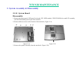
2.2.11 System Board
Disassembly
1. Remove the battery pack, LED panel, keyboard, CPU, HDD module, CD/DVD-ROM drive and LCD assembly.
(See the Disassembly parts in previous sections.)
2. Remove thirteen screws on the bottom of the notebook. (Figure 2-19)
Figure 2-19
Figure 2-20
3. Remove the speaker assembly from the notebook. (Figure 2-20)
59
7170 N/B MAINTENANCE
2. System Assembly & Disassembly
4. Remove two screws on the rear side of the notebook. Then remove three screws fastening the base unit cover and
one screw in the CPU compartment. (Figure 2-21)
Figure 2-21
Figure 2-22
5. Remove two screws fastening the LED board. (Figure 2-22)
60
7170 N/B MAINTENANCE
2. System Assembly & Disassembly
6. Lift up the base unit cover and disconnect the touchpad cable. (Figure 2-23)
Figure 2-23
Figure 2-24
7. Remove three screws from the base. (Figure 2-24)
61
7170 N/B MAINTENANCE
2. System Assembly & Disassembly
8. Disconnect two cables from the system board and lift up the base unit to access the system board. (Figure 2-25)
Figure 2-25
Reassembly
1. Reconnect two cables to the system board.
2. Replace three screws fastening the base unit.
3. Reconnect the touchpad cable and replace the base unit cover.
4. Replace two screws fastening the LED board.
5. Replace one screw in the CPU compartment and three screws fastening the base unit cover.
5. Replace two screws on the rear side of the notebook.
6. Replace the speaker assembly.
7. Replace thirteen screws on the bottom of the notebook.
8. Replace the battery pack, LED panel, keyboard, CPU, HDD module, CD/DVD-ROM drive and LCD assembly.
62
7170 N/B MAINTENANCE
2. System Assembly & Disassembly
2.2.12 Touchpad
Disassembly
1. Remove the base unit cover. (See steps 1-6 in section 2.2.11 Disassembly.)
2. Remove the six screws to lift up the touchpad holder and touchpad panel. (Figure 2-26)
Figure 2-26
Reassembly
1. Replace the touchpad holder and touchpad panel, and secure with six screws.
2. Assemble the notebook. (See section 2.2.11 Reassembly.)
63
7170 N/B MAINTENANCE
2. System Assembly & Disassembly
2.2.13 Modem Card
Disassembly
1. Disassemble the notebook to access the system board. (See section 2.2.11 Disassembly.)
2. Remove the two screws fastening the modem card. (Figure 2-27)
Figure 2-27
3. Disconnect the cable from the modem card. (Figure 2-28)
Figure 2-28
Reassembly
1. Reconnect the cable to the modem card and secure the modem card with two screws.
2. Assemble the notebook. (See section 2.2.11 Reassembly.)
64
7170 N/B MAINTENANCE
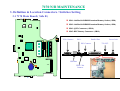
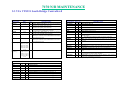
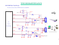
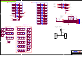
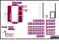
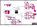
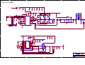
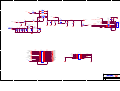
3. Definition & Location Connectors / Switches Setting
3.1 7170 Main Board ( Side A-1 )
J26, J27 J2
J4
J3
J1
J1 : PS2 Connector. ( SH17 )
J10
J8
J6
J2 : RJ11 Phone Jack. ( SH18 )
J7
J9
J3 : IEEE 1394 Connector. ( SH14 )
J4 : External VGA Connector. ( SH9 )
J6 : Modem Daughter Board To RJ11 Connector. ( SH18 )
J7 : Main Board To DC Power Board Connector. ( SH22 )
J11
J12
J8 : LCD Panel Module Connector. ( SH9 )
SW1
J13
J15
J9 : Easy Start Button Connector. ( SH17 )
J10 : Main Board To DC Power Board Connector. ( SH22 )
J11 : RJ45 LAN Connector. ( SH18 )
J509
J14
J12 : CPU FAN Connector. ( SH17 )
J20
J13 : CDCD-ROM Device Connector. ( SH12 )
J16
J18
J14 : PCMCIA Card Bus Connector. ( SH14 )
J17
J15 : Internal Keyboard Connector. ( SH17 )
J30
J21
SW4
J22
SW3
J23 J24 J25
VR1
65
7170 N/B MAINTENANCE
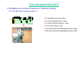
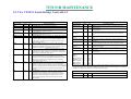
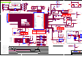
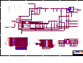
3. Definition & Location Connectors / Switches Setting
3.1 7170 Main Board ( Side A-2 )
J26, J27 J2
J4
J3
J1
J16 : Battery Connector. ( SH21 )
J10
J8
J6
J7
J9
J17 : Touch Pad Connector. ( SH15 )
J18 : Modem Daughter Board ACAC-Link Connector. ( SH18 )
J20 : Hard Disk Connector. ( SH12 )
J21,J22 : L,R Internal Speaker Connector. ( SH13 )
J23 : External Micro Phone Jack. ( SH13 )
J11
J12
J24 : Line In. ( SH13 )
SW1
J13
J15
J25 : Line Out Phone Jack. ( SH13 )
J26,J27 : USB Port Connector. ( SH15 )
J30 : Internal Micro Phone Jack. ( SH13 )
J509
J14
VR1 : Volume Control. ( SH13 )
J20
SW1 : Panel Type Select. ( SH6 )
J16
J18
SW3 : EE-Mail Button. ( SH17 )
J17
SW4 : Cover Switch. ( SH17 )
J30
J21
SW4
J22
SW3
J23 J24 J25
VR1
66
7170 N/B MAINTENANCE
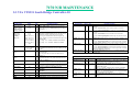
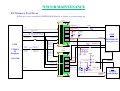
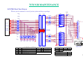
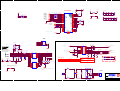
3. Definition & Location Connectors / Switches Setting
3.1 7170 Main Board ( Side B )
J501 : 144 Pin SOSO-DIMM Extension Memory Socket. ( SH8 )
J502 : 144 Pin SOSO-DIMM Extension Memory Socket. ( SH8 )
J503 : QTC Connector. ( SH19 )
J505 : RTC Battery Connector. ( SH12 )
VGA Connect.
RJ11.
Parallel Port
PS/2 Connect.
J502
Power Jack
TV OUT.
J501
USB Port
J505
J503
IEEE 1394
Connect.
67
7170 N/B MAINTENANCE
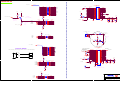
3. Definition & Location Connectors / Switches Setting
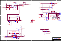
3.2 7170 DC Power Board ( Side A )
J1
J5
J4
J1 : Parallel Port Connector. ( SH3 )
PJ2
J3
PJ1
J3 : Inverter Board Connector. ( SH2 )
J4 : Power Jack Board Connector. ( SH2 )
J5 : TV Out Connector. ( SH3 )
PJ1 : DC Power Board To Main Board Connector. ( SH2 )
PJ2 : DC Power Board To Main Board Connector. ( SH2 )
68
7170 N/B MAINTENANCE
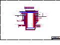
3. Definition & Location Connectors / Switches Setting
3.3 7170 ESB Board ( Side A,B )
SW1
SW2
SW3
SW4
SW5
J501 : Easy Start Button Connector.
SW6
SW1 : Programmable Easy Start Button Switch.
SW2 : Programmable Easy Start Button Switch.
SW3 : Programmable Easy Start Button Switch.
J501
SW4 : Programmable Easy Start Button Switch.
SW5 : Programmable Easy Start Button Switch.
SW6 : Programmable Easy Start Button Power Switch.
3.4 7170 Touch Pad Board ( Side A,B )
J501 : Touch Pad Board To Touch Pad Connector.
J502 : Touch Pad Board To Main Board Connector.
SW1 : Scroll Up Button Switch.
J1
SW2 : Left Button Switch.
J501
SW2
SW1
J502
SW4
SW3
SW3 : Right Button Switch.
SW4 : Scroll Down Button Switch.
69
7170 N/B MAINTENANCE
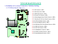
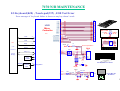
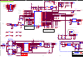
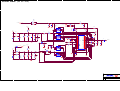
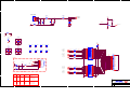
4. Definition & Location Major Components
4.1 7170 Main Board ( Side A )
U1 : PIII/Celeron
PIII/Celeron FCFC-PGA 370370-Pin Socket. ( SH4 )
U2 : GL528SM Thermal Recorder. ( SH4 )
U1
U6 : 93C468 Serial EEPROM. ( SH11 )
U8 : 28F02028F020-PLCC Flash ROM BIOS. ( SH15)
U2
U10 : NM24C02N. ( SH14 )
U12 : VT8231 South Bridge. ( SH10 )
PU4
U25
U16 : ALC200 Audio Codec.
Codec. ( SH13 )
U18 : TPA0202 Audio Amplifier. ( SH13 )
U19 : 74VHV164. ( SH9 )
U21
J509
U10
U21 : PCI 4410GHK PCMCIA Card Bus Controller. ( SH14 )
U8
U25 : LSI 80227. ( SH18 )
U6
U12
PU4 : SC 1401CSS. ( SH20 )
U16 U18
U19
70
7170 N/B MAINTENANCE
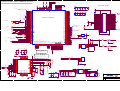
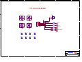
4. Definition & Location Major Components
4.1 7170 Main Board ( Side B )
U500 : TSB 41AB1 1394 PHY. ( SH14 )
U501 : TWINSTER North Bridge. ( SH6 )
?U
U500
U502 : H8/34347 Micro Controller. ( SH17 )
U511
U503 : ICS9248ICS9248-195 Clock Generator. ( SH16 )
PU501
U505 : SN74CBTD3384 Level Shift. ( SH17)
PU500
PU502
PU504
U511 : CH7005C TV Encoder. ( SH9 )
U501
?U
U1
PU504 : MAX1717. ( SH20 )
U2
PU6 : TL594C PWM. ( SH22 )
U3
U5?
U4
U502
PU508
U503
J502
J501
U505
J505
J503
?
U508
71
7170 N/B MAINTENANCE
5. Pin Descriptions Of Major Components
5.1 Pentium III/Celeron µPGA2 CPU-1
Alphabetical Signal Reference
Signal Name
A[35:3]#
A20M#
ADS#
AERR#
AP[1:0]#
BCLK
I/O
Signal Description
I/O The A[35:3]# (Address) signals define a 2 36 -byte physical memory
GTL+ address space. When ADS# is active, these signals transmit the
address of a transaction; when ADS# is inactive, these signals
transmit transaction information. These signals must be connected to
the appropriate pins/balls of both agents on the system bus. The
A[35:24]# signals are protected with the AP1# parity signal,
and the A[23:3]# signals are protected with the AP0# parity signal.
On the active-to-inactive transition of RESET#, each processor bus
agent samples A[35:3]# signals to determine its power-on
configuration. See Section 4 of this document and the PentiumII
Processor Developer’s Manual for details.
I
If the A20M# (Address-20 Mask) input signal is asserted, the
1.5V processor masks physical address bit 20 (A20#) before looking up a
Tolerant line in any internal cache and before driving a read/write transaction
on the bus. Asserting A20M# emulates the 8086 processor's address
wrap-around at the 1-Mbyte boundary. Assertion of A20M# is only
supported in Real mode.
I/O The ADS# (Address Strobe) signal is asserted to indicate the validity
GTL+ of a transaction address on the A[35:3]# signals. Both bus agents
observe the ADS# activation to begin parity checking, protocol
checking, address decode, internal snoop or deferred reply ID match
operations associated with the new transaction. This signal must be
connected to the appropriate pins/balls on both agents on the system
bus.
I/O The AERR# (Address Parity Error) signal is observed and driven by
GTL+ both system bus agents, and if used, must be connected to the
appropriate pins/balls of both agents on the system bus. AERR#
observation is optionally enabled during power-on configuration; if
enabled, a valid assertion of AERR# aborts the current transaction.
If AERR# observation is disabled during power-on configuration, a
central agent may handle an assertion of AERR# as appropriate to the
error handling architecture of the system.
I/O The AP[1:0]# (Address Parity) signals are driven by the request
GTL+ initiator along with ADS#, A[35:3]#, REQ[4:0]# and RP#. AP1#
covers A[35:24]#. AP0# covers A[23:3]#. A correct parity signal is
high if an even number of covered signals are low and low if an odd
number of covered signals are low. This allows parity to be high when
all the covered signals are high. AP[1:0]# should be connected to the
appropriate pins/balls on both agents on the system bus.
I
The BCLK (Bus Clock) signal determines the system bus frequency.
2.5V Both system bus agents must receive this signal to drive their outputs
Tolerant and latch their inputs on the BCLK rising edge. All external timing
parameters are specified with respect to the BCLK signal.
Signal Name
BERR#
BINIT#
BNR#
BP[3:2]#
BPM[1:0]#
I/O
Signal Description
I/O The BERR# (Bus Error) signal is asserted to indicate an
GTL+ unrecoverable error without a bus protocol violation. It may be driven
by either system bus agent and must be connected to the appropriate
pins/balls of both agents, if used. However, the mobile Pentium III
processors do not observe assertions of the BERR# signal.
BERR# assertion conditions are defined by the system configuration.
Configuration options enable the BERR# driver as follows:
• Enabled or disabled
• Asserted optionally for internal errors along with IERR#
• Asserted optionally by the request initiator of a bus transaction after
it observes an error
• Asserted by any bus agent when it observes an error in a bus
transaction
I/O- The BINIT# (Bus Initialization) signal may be observed and driven
GTL+ by both system bus agents and must be connected to the appropriate
pins/balls of both agents, if used. If the BINIT# driver is enabled
during the power-on configuration, BINIT# is asserted to signal any
bus condition that prevents reliable future information.
If BINIT# is enabled during power-on configuration, and BINIT# is
sampled asserted, all bus state machines are reset and any data which
was in transit is lost. All agents reset their rotating ID for bus
arbitration to the state after reset, and internal count information is
lost. The L1 and L2 caches are not affected.
If BINIT# is disabled during power-on configuration, a central agent
may handle an assertion of BINIT# as appropriate to the Machine
Check Architecture (MCA) of the system.
I/O- The BNR# (Block Next Request) signal is used to assert a bus stall by
GTL+ any bus agent that is unable to accept new bus transactions. During a
bus stall, the current bus owner cannot issue any new transactions.
Since multiple agents may need to request a bus stall simultaneously,
BNR# is a wired-OR signal that must be connected to the appropriate
pins/balls of both agents on the system bus. In order to avoid wire-OR
glitches associated with simultaneous edge transitions driven by
multiple drivers, BNR# is activated on specific clock edges and
sampled on specific clock edges.
I/O The BP[3:2]# (Breakpoint) signals are the System Support group
GTL+ Breakpoint signals. They are outputs from the processor that indicate
the status of breakpoints.
I/O The BPM[1:0]# (Breakpoint Monitor) signals are breakpoint and
GTL+ performance monitor signals. They are outputs from the processor
that indicate the status of breakpoints and programmable counters
used for monitoring processor performance.
72
7170 N/B MAINTENANCE
5.1 Pentium III/Celeron µPGA2 CPU-2
Alphabetical Signal Reference
Signal Name
BPRI#
BREQ0#
BSEL[1:0]
CLKREF
CMOSREF
D[63:0]#
I/O
Signal Description
I
The BPRI# (Bus Priority Request) signal is used to arbitrate for
GTL+ ownership of the system bus. It must be connected to the appropriate
pins/balls on both agents on the system bus. Observing BPRI# active
(as asserted by the priority agent) causes the processor to stop issuing
new requests, unless such requests are part of an ongoing locked
operation. The priority agent keeps BPRI# asserted until all of its
requests are completed and then releases the bus by deasserting
BPRI#.
I/O The BREQ0# (Bus Request) signal is a processor Arbitration Bus
GTL+ signal. The processor indicates that it wants ownership of the system
bus by asserting the BREQ0# signal.
During power-up configuration, the central agent must assert the
BREQ0# bus signal. The processor samples BREQ0# on the activeto-inactive transition of RESET#.
I
The BSEL[1:0] (Select Processor System Bus Speed) signal is used to
1.5V configure the processor for the system bus frequency. Table 38 shows
Tolerant the encoding scheme for BSEL[1:0]. The only supported system bus
frequency for the mobile Pentium III processor is 100 MHz. If
another frequency is used or if the BSEL[1:0] signals are not driven
with "1" then the processor is not guaranteed to function properly.
BSEL[1:0] Encoding
BSEL[1:0]
System Bus Frequency
00
66 MHz
01
100 MHz
10
Reserved
11
133 MHz
Analog The CLKREF (System Bus Clock Reference) signal provides a
reference voltage to define the trip point for the BCLK signal. This
signal should be connected to a resistor divider to generate 1.25V
from the 2.5-V supply.
Analog The CMOSREF (CMOS Reference Voltage) signal provides a DC
level reference voltage for the CMOS input buffers. A voltage divider
should be used to divide a stable voltage plane (e.g., 2.5V or 3.3V).
This signal must be provided with a DC voltage that meets the
VCMOSREF specification from Table 13.
I/O The D[63:0]# (Data) signals are the data signals. These signals
GTL+ provide a 64-bit data path between both system bus agents, and must
be connected to the appropriate pins/balls on both agents. The data
driver asserts DRDY# to indicate a valid data transfer.
Signal Name
DBSY#
DEFER#
DEP[7:0]#
DRDY#
EDGCTRLP
FERR#
FLUSH#
I/O
Signal Description
I/O- The DBSY# (Data Bus Busy) signal is asserted by the agent
GTL+ responsible for driving data on the system bus to indicate that the data
bus is in use. The data bus is released after DBSY# is deasserted. This
signal must be connected to the appropriate pins/balls on both agents
on the system bus.
I
The DEFER# (Defer) signal is asserted by an agent to indicate that
GTL+ the transaction cannot be guaranteed in-order completion. Assertion
of DEFER# is normally the responsibility of the addressed memory
agent or I/O agent. This signal must be connected to the appropriate
pins/balls on both agents on the system bus.
I/O The DEP[7:0]# (Data Bus ECC Protection) signals provide optional
GTL+ ECC protection for the data bus. They are driven by the agent
responsible for driving D[63:0]#, and must be connected to the
appropriate pins/balls on both agents on the system bus if they are
used. During power-on configuration, DEP[7:0]# signals can be
enabled for ECC checking or disabled for no checking.
I/O The DRDY# (Data Ready) signal is asserted by the data driver on
GTL+ each data transfer, indicating valid data on the data bus. In a multicycle data transfer, DRDY# can be deasserted to insert idle clocks.
This signal must be connected to the appropriate pins/balls on both
agents on the system bus.
Analog The EDGCTRLP (Edge Rate Control) signal is used to configure the
edge rate of the GTL+ output buffers. Connect the signal to VSS with
a 110-Ω, 1% resistor.
O
The FERR# (Floating-point Error) signal is asserted when the
1.5V processor detects an unmasked floating-point error. FERR# is similar
Tolerant to the ERROR# signal on the Intel 387 coprocessor, and it is included
Open- for compatibility with systems using DOS-type floating-point error
drain) reporting.
I
When the FLUSH# (Flush) input signal is asserted, the processor
1.5V writes back all internal cache lines in the Modified state and
Tolerant invalidates all internal cache lines. At the completion of a flush
operation, the processor issues a Flush Acknowledge transaction. The
processor stops caching any new data while the FLUSH# signal
remains asserted.
On the active-to-inactive transition of RESET#, each processor bus
agent samples FLUSH# to determine its power-on configuration.
73
7170 N/B MAINTENANCE
5.1 Pentium III/Celeron µPGA2 CPU-3
Alphabetical Signal Reference
Signal Name
GHI#
HIT#, HITM#
IERR#
IGNNE#
INIT#
I/O
Signal Description
I
The GHI# signal controls which operating mode bus ratio is selected
1.5V in a mobile Pentium III processor featuring Intel SpeedStep
Tolerant technology. On the processor featuring Intel SpeedStep technology,
this signal is latched when BCLK restarts in Deep Sleep state and
determines which of two bus ratios is selected for operation. This
signal is ignored when the processor is not in the Deep Sleep state.
This signal is a "Don't Care" on processors that do not feature Intel
SpeedStep technology. This signal has an on-die pull-up to VccT and
should be driven with an Open-drain driver with no external pull-up.
I/O The HIT# (Snoop Hit) and HITM# (Hit Modified) signals convey
GTL+ transaction snoop operation results, and must be connected to the
appropriate pins/balls on both agents on the system bus.
Either bus agent can assert both HIT# and HITM# together to indicate
that it requires a snoop stall, which can be continued by reasserting
HIT# and HITM# together.
O
The IERR# (Internal Error) signal is asserted by the processor as the
1.5V result of an internal error.Assertion of IERR# is usually accompanied
Tolerant by a SHUTDOWN transaction on the system bus.
Open- This transaction may optionally be converted to an external error
drain signal (e.g., NMI) by system logic. The processor will keep IERR#
asserted until it is handled in software or with the assertion of
RESET#, BINIT, or INIT#.
I
The IGNNE# (Ignore Numeric Error) signal is asserted to force the
1.5V processor to ignore a numeric error and continue to execute nonTolerant control floating-point instructions. If IGNNE# is deasserted, the
processor freezes on a non-control floating-point instruction if a
previous instruction caused an error. IGNNE# has no affect when the
NE bit in control register 0 (CR0) is set.
I
The INIT# (Initialization) signal is asserted to reset integer registers
1.5V inside the processor without affecting the internal (L1 or L2) caches
Tolerant or the floating-point registers. The processor begins execution at the
power-on reset vector configured during power-on configuration. The
processor continues to handle snoop requests during INIT# assertion.
INIT# is an asynchronous input.
If INIT# is sampled active on RESET#'s active-to-inactive transition,
then the processor executes its built-in self test (BIST).
Signal Name
INTR
LINT[1:0]
LOCK#
NMI
I/O
Signal Description
I
The INTR (Interrupt) signal indicates that an external interrupt has
1.5V been generated. INTR becomes the LINT0 signal when the APIC is
Tolerant enabled. The interrupt is maskable using the IF bit in the EFLAGS
register. If the IF bit is set, the processor vectors to the interrupt
handler after completing the current instruction execution. Upon
recognizing the interrupt request, the processor issues a single
Interrupt Acknowledge (INTA) bus transaction. INTR must remain
active until the INTA bus transaction to guarantee its recognition.
I
The LINT[1:0] (Local APIC Interrupt) signals must be connected to
1.5V the appropriate pins/balls of all APIC bus agents, including the
Tolerant processor and the system logic or I/O APIC component. When APIC
is disabled, the LINT0 signal becomes INTR, a maskable interrupt
request signal, and LINT1 becomes NMI, a non-maskable interrupt.
INTR and NMI are backward compatible with the same signals for
the Pentium processor. Both signals are asynchronous inputs.
Both of these signals must be software configured by programming
the APIC register space to be used either as NMI/INTR or LINT[1:0]
in the BIOS. If the APIC is enabled at reset, then LINT[1:0] is the
default configuration.
I/O The LOCK# (Lock) signal indicates to the system that a sequence of
GTL+ transactions must occur atomically. This signal must be connected to
the appropriate pins/balls on both agents on the system bus. For a
locked sequence of transactions, LOCK# is asserted from the
beginning of the first transaction through the end of the last
transaction.
When the priority agent asserts BPRI# to arbitrate for bus ownership,
it waits until it observes LOCK# deasserted. This enables the
processor to retain bus ownership throughout the bus locked operation
and guarantee the atomicity of lock.
I
The NMI (Non-Maskable Interrupt) indicates that an external
1.5V interrupt has been generated. NMI becomes the LINT1 signal when
Tolerant the APIC is disabled. Asserting NMI causes an interrupt with an
internally supplied vector value of 2. An external interruptacknowledge transaction is not generated. If NMI is asserted during
the execution of an NMI service routine, it remains pending and is
recognized after the IRET is executed by the NMI service routine. At
most, one assertion of NMI is held pending. NMI is rising edge
sensitive.
74
7170 N/B MAINTENANCE
5.1 Pentium III/Celeron µPGA2 CPU-4
Alphabetical Signal Reference
Signal Name
PICCLK
PICD[1:0]
PLL1, PLL2
PRDY#
PREQ#
PWRGOOD
I/O
I
2.5V
Tolerant
I/O
1.5V
Tolerant
Opendrain
Signal Description
The PICCLK (APIC Clock) signal is an input clock to the processor
and system logic or I/O APIC that is required for operation of the
processor, system logic, and I/O APIC components on the APIC bus.
The PICD[1:0] (APIC Data) signals are used for bi-directional serial
message passing on the APIC bus. They must be connected to the
appropriate pins/balls of all APIC bus agents, including the processor
and the system logic or I/O APIC components. If the PICD0 signal is
sampled low on the active-to-inactive transition of the RESET#
signal, then the APIC is hardware disabled.
Analog The PLL1 and PLL2 signals provide isolated analog decoupling is
required for the internal PLL. See Section 3.2.2 for a description of
the analog decoupling circuit.
O
The PRDY# (Probe Ready) signal is a processor output used by
GTL+ debug tools to determine processor debug readiness.
I
The PREQ# (Probe Request) signal is used by debug tools to request
1.5V debug operation of the processor.
Tolerant
I
PWRGOOD (Power Good) is a 2.5-V tolerant input. The processor
2.5V requires this signal to be a clean indication that clocks and the power
Tolerant supplies (Vcc, VccT, etc.) are stable and within their specifications.
Clean implies that the signal will remain low, (capable of sinking
leakage current) and without glitches, from the time that the power
supplies are turned on, until they come within specification. The
signal will then transition monotonically to a high (2.5V) state. Figure
26 illustrates the relationship of PWRGOOD to other system signals.
PWRGOOD can be driven inactive at any time, but clocks and power
must again be stable before the rising edge of PWRGOOD. It must
also meet the minimum pulse width specified in Table 17 (Section
3.7) and be followed by a 1 ms RESET# pulse.
PWRGOOD Relationship at Power On
The PWRGOOD signal, which must be supplied to the processor, is used to protect internal circuits
against voltage sequencing issues. The PWRGOOD signal should be driven high throughout boundary
scan operation.
Signal Name
REQ[4:0]#
RESET#
RP#
PWRGOOD Relationship at Power On
RS[2:0]#
I/O
Signal Description
I/O The REQ[4:0]# (Request Command) signals must be connected to the
GTL+ appropriate pins/balls on both agents on the system bus. They are
asserted by the current bus owner when it drives A[35:3]# to define
the currently active transaction type.
I
Asserting the RESET# signal resets the processor to a known state
GTL+ and invalidates the L1 and L2 caches without writing back Modified
(M state) lines. For a power-on type reset, RESET# must stay active
for at least 1 msec after Vcc and BCLK have reached their proper DC
and AC specifications and after PWRGOOD has been asserted. When
observing active RESET#, all bus agents will deassert their outputs
within two clocks. RESET# is the only GTL+ signal that does
not have on-die GTL+ termination. A 56.2Ω1% terminating resistor
connected to VccT is required.
A number of bus signals are sampled at the active-to-inactive
transition of RESET# for the power-on configuration. The
configuration options are described in Section 4 and in the Pentium II
Processor Developer’s Manual.
Unless its outputs are tri-stated during power-on configuration, after
an active-to-inactive transition of RESET#, the processor optionally
executes its built-in self-test (BIST) and begins program execution at
reset-vector 000FFFF0H or FFFFFFF0H. RESET# must be connected
to the appropriate pins/balls on both agents on the system bus.
I/O The RP# (Request Parity) signal is driven by the request initiator and
GTL+ provides parity protection on ADS# and REQ[4:0]#. RP# should be
connected to the appropriate pins/balls on both agents on the system
bus.
A correct parity signal is high if an even number of covered signals
are low and low if an odd number of covered signals are low. This
definition allows parity to be high when all covered signals are high.
I
The RS[2:0]# (Response Status) signals are driven by the response
GTL+ agent (the agent responsible for completion of the current transaction)
and must be connected to the appropriate pins/balls on both agents on
the system bus.
75
7170 N/B MAINTENANCE
5.1 Pentium III/Celeron µPGA2 CPU-5
PWRGOOD Relationship at Power On
Signal Name
RSP#
RSVD
RTTIMPEDP
SLP#
SMI#
STPCLK#
TCK
I/O
Signal Description
I
The RSP# (Response Parity) signal is driven by the response agent
GTL+ (the agent responsible for completion of the current transaction)
during assertion of RS[2:0]#. RSP# provides parity protection for
RS[2:0]#. RSP# should be connected to the appropriate pins/balls on
both agents on the system bus.
A correct parity signal is high if an even number of covered signals
are low, and it is low if an odd number of covered signals are low.
During Idle state of RS[2:0]# (RS[2:0]#=000), RSP# is also high
since it is not driven by any agent guaranteeing correct parity.
TBD The RSVD (Reserved) signal is currently unimplemented but is
reserved for future use. Leave this signal unconnected. Intel
recommends that a routing channel for this signal be allocated.
Analog The RTTIMPEDP (RTT Impedance/PMOS) signal is used to
configure the on-die GTL+ termination. Connect the RTTIMPEDP
signal to VSS with a 56.2-Ω, 1% resistor.
I
The SLP# (Sleep) signal, when asserted in the Stop Grant state,
1.5V causes the processor to enter the Sleep state. During the Sleep state,
Tolerant the processor stops providing internal clock signals to all units,
leaving only the Phase-Locked Loop (PLL) still running. The
processor will not recognize snoop and interrupts in the Sleep state.
The processor will only recognize changes in the SLP#, STPCLK#
and RESET# signals while in the Sleep state. If SLP# is deasserted,
the processor exits Sleep state and returns to the Stop Grant state in
which it restarts its internal clock to the bus and
APIC processor units.
I
The SMI# (System Management Interrupt) is asserted asynchronously
1.5V by system logic. On accepting a System Management Interrupt, the
Tolerant processor saves the current state and enters System Management
Mode (SMM). An SMI Acknowledge transaction is issued, and the
processor begins program execution from the SMM handler.
I
The STPCLK# (Stop Clock) signal, when asserted, causes the
1.5V processor to enter a low-power Stop Grant state. The processor issues
Tolerant a Stop Grant Acknowledge special transaction and stops providing
internal clock signals to all units except the bus and APIC units. The
processor continues to snoop bus transactions and service interrupts
while in the Stop Grant state. When STPCLK# is deasserted, the
processor restarts its internal clock to all units and resumes execution.
The assertion of STPCLK# has no affect on the bus clock.
I
The TCK (Test Clock) signal provides the clock input for the test bus
1.5V (also known as the test access port).
Tolerant
Signal Name
TDI
TDO
TESTHI
TESTLO[2:1]
TESTP
THERMDA,
THERMDC
TMS
TRDY#
TRST#
I/O
I
1.5V
Tolerant
O
1.5V
Tolerant
Opendrain
I
1.5V
Tolerant
I
1.5V
Tolerant
Analog
Signal Description
The TDI (Test Data In) signal transfers serial test data to the
processor. TDI provides the serial input needed for JTAG support.
The TDO (Test Data Out) signal transfers serial test data from the
processor. TDO provides the serial output needed for JTAG support.
The TESTHI (Test input High) is used during processor test and
needs to be pulled high during normal operation.
The TESTLO[2:1] (Test input Low) signals are used during processor
test and needs to be pulled to ground during normal operation.
The TESTP (Test Point) signals are connected to Vcc and Vss at
opposite ends of the die. These signals can be used to monitor the Vcc
level on the die. Route the TESTP signals to test points or leave them
unconnected. Do not short the TESTP signals together.
Analog The THERMDA (Thermal Diode Anode) and THERMDC (Thermal
Diode Cathode) signals connect to the anode and cathode of the ondie thermal diode.
I
The TMS (Test Mode Select) signal is a JTAG support signal used by
1.5V debug tools.
Tolerant
I
The TRDY# (Target Ready) signal is asserted by the target to indicate
GTL+ that the target is ready to receive write or implicit write-back data
transfer. TRDY# must be connected to the appropriate pins/balls on
both agents on the system bus.
I
The TRST# (Test Reset) signal resets the Test Access Port (TAP)
1.5V logic. The mobile Pentium III processors do not self-reset during
Tolerant power on; therefore, it is necessary to drive this signal low during
power-on reset.
76
7170 N/B MAINTENANCE
5.1 Pentium III/Celeron µPGA2 CPU-6
PWRGOOD Relationship at Power On
Signal Name
VID[4:0]
I/O
Signal Description
O - The VID[4:0] (Voltage ID) pins/balls can be used to support
Open- automatic selection of power supply voltages. These pins/balls are not
drain signals, they are either an open circuit or a short to VSS on the
processor substrate. The combination of opens and shorts encodes the
voltage required by the processor. External to pull-ups are required to
sense the encoded VID. For processors that have Intel SpeedStep
technology enabled, VID[4:0] encode the voltage required in the
battery-optimized mode. VID[4:0] are needed to cleanly support
voltage specification changes on mobile Pentium III processors. The
voltage encoded by VID[4:0] is defined in Table 39. A "1" in this
table refers to an open pin/ball and a "0" refers to a short to VSS. The
power supply must provide the requested voltage or disable itself.
Please note that in order to implement VID on the BGA2 package,
some VID[4:0] balls may be depopulated. For the BGA2 package, a
"1" in Table 39 implies that the corresponding VID ball is
depopulated, while a "0" implies that the corresponding VID ball is
not depopulated.
But on the Micro-PGA2 package, VID[4:0] pins are not depopulated.
77
7170 N/B MAINTENANCE
5.2 VIA VT8603 Twister North Bridge Controller-1
VT8603 / Twister OVERVIEW
Twister (VT8603) is a high performance, cost-effective and energy efficient SMA chip set for the implementation of
mobile personal computer systems with 66 MHz, 100 MHz and 133 MHz CPU host bus (“Front Side Bus”) frequencies
and based on 64-bit Socket-370 and Slot-1 (Intel Pentium III, Pentium-II and Celeron) super-scalar processors.
78
7170 N/B MAINTENANCE
5.2 VIA VT8603 Twister North Bridge Controller-2
Twister integrates VIA’s VT82C694X system controller, S3’s Savage4 2D/3D graphics accelerator and S3’s flat panel
interfaces into a single 552 BGA package. The Twister SMA system controller provides superior performance between
the CPU, DRAM and PCI bus with pipelined, burst, and concurrent operation.
Twister supports six banks of DRAMs up to 1.5Gbyte of system memory with 256Mbit DRAM technology. The DRAM
controller supports standard Synchronous DRAM (SDRAM) and Virtual Channel SDRAM (VC SDRAM), in a flexible
mix /match manner. The Synchronous DRAM interface allows zero wait state bursting between the DRAM and the data
buffers at 100/133 MHz. The six banks of DRAM can be composed of an arbitrary mixture of 1M / 2M / 4M / 8M / 16M
/32MxN DRAMs. The DRAM controller can run at either the host CPU Front Side Bus frequency (100 / 133 MHz) or
pseudo-synchronous to the CPU FSB frequency (PC100 with the FSB at 133 MHz or PC133 with the FSB at 100 MHz)
with built-in PLL timing control.
Twister supports a 32-bit 3.3 / 5V system bus (PCI) that is synchronous / pseudo-synchronous to the CPU bus. The chip
Also contains a built-in bus-to-bus bridge to allow simultaneous concurrent operations on each bus. Five levels
(doublewords) of post write buffers are included to allow for concurrent CPU and PCI operation. For PCI master operation,
forty-eight levels(doublewords) of post write buffers and sixteen levels (doublewords) of prefetch buffers are included for
concurrent PCI bus and DRAM/cache accesses. The chip also supports enhanced PCI bus commands such as MemoryRead-Line, Memory-Read-Multiple and Memory-Write-Invalid commands to minimize snoop overhead. In addition,
advanced features are supported such as snoop ahead, snoop filtering, L1 write-back forward to PCI master, and L1 writeback merged with PCI post write buffers to minimize PCI master read latency and DRAM utilization. Delay transaction
and read caching mechanisms are also implemented for further improvement of overall system performance.
Twister also integrates S3’s Savage graphics accelerator into a single chip. Twister brings mainstream graphics
performance to the Value PC with leading-edge 2D, 3D and DVD video acceleration into a cost effective package. Based
on its capabilities, Twister is an ideal solution for the consumer, corporate mobile users and entry level professionals.
The industry’s first integrated AGP 4X solution, Twister combines AGP 4X performance with S3’s DX6 texture
Compression (S3TC) and massive 2Kx2K textures to deliver unprecedented 3D performance and image quality for the
Value PC mobile market.
79
7170 N/B MAINTENANCE
5.2 VIA VT8603 Twister North Bridge Controller-3
The 352-pin VT8231 BGA PCI-LPC bridge supports four levels (doublewords) of line buffers, type F DMA transfers and
delay transaction to allow efficient PCI bus utilization and (PCI-2.2 compliant). The VT8231 also includes an integrated
Super I/O, integrated DS12885 style real time clock with extended 256 byte CMOS RAM, integrated master mode
enhanced IDE controller with full scatter / gather capability and extension to UltraDMA-33 / 66 / 100 for 33 / 66 / 100
MB/sec transfer rate, integrated four USB interface with root hub and two function ports with built-in physical layer
transceivers, Distributed DMA support, integrated AC-97 link for basic audio and HSP based modem functions, integrated
hardware monitoring and OnNow / ACPI compliant advanced configuration and power management interface. The
VT8231 also has an integrated MAC and 10Mbit PHY for LAN connection. It can bypass the internal PHY with external
home PNA with a 1Mbit PHY or a 10/100Mbit PHY through the MII interface.
For sophisticated power management, Twister provides independent clock stop control for the CPU / SDRAM and PCI and
Dynamic CKE control for powering down of the SDRAM. A separate suspend-well plane is implemented for the SDRAM
control signals for Suspend-to-DRAM operation. Coupled with the VT8231 south bridge chip, a complete power conscious
PC main board can be implemented with no external TTLs.
High-Performance 3D Accelerator
Featuring a new super-pipelined 128-bit engine, Twister utilizes a single cycle architecture that provides high performance
along with superior image quality. Several new features enhance the 3D architecture, including single-pass multitexturing,
anisotropic filtering, and an 8-bit stencil buffer. Twister also offers the industry’s only simultaneous usage of single-pass
multitexturing and single-cycle trilinear filtering ?enabling stunning image quality without performance loss. Twister
further enhances image quality with true 32-bit color rendering throughout the 3D pipeline to produce more vivid and
realistic images. Twister’s advanced triangle setup engine provides industry leading 3D performance for a realistic user
experience in games and other interactive 3D applications. The 3D engine is optimized for AGP texturing from system
memory.
128-bit 2D Graphics Engine
Twister’s advanced 128-bit 2D graphics engine delivers high-speed 2D acceleration for productivity applications. Several
enhancements have been made to the 2D architecture to optimize SMA performance and to provide acceleration in all color
depths.
80
7170 N/B MAINTENANCE
5.2 VIA VT8603 Twister North Bridge Controller-4
DVD Playback and Video Conferencing
Twister provides the ideal architecture for high quality MPEG-2 based DVD applications and video conferencing. For DVD
playback, Twister’s video accelerator offloads the CPU by performing the planar to packed format conversion and motion
compensation tasks, while its enhanced scaling algorithm delivers incredible full-screen video playback. For video
conferencing, Twister’s multiple video windows enable a cost effective solution.
LCD and Flat Panel Monitor Support
Twister supports a wide variety of DSTN or TFT panels through a 36-bit interface. This includes support for VGA, SVGA,
XGA, SXGA+, UXGA, and UXGA+ TFT color panels with 9-bit, 12-bit, 18-bit (both 1 pixel/clock and 2 pixels/clock), and
24-bit interfaces. Enhanced STN hardware with 256 gray scale support and advanced frame rate control to provide up to 16.7
million colors. In addition, the integrated 2-channel LVDS interface can support another panel. All resolutions are supported
up to 1280x1024. The integrated ZV-Port allows display of video from an external source.
An alternative to the 36-bit panel interface is a 12-bit interface to a TMDS encoder. This interface is Digital Visual Interface
(DVI) 1.0 compliant.
81
7170 N/B MAINTENANCE
5.2 VIA VT8603 Twister North Bridge Controller-5
VT8603 / Twister Pin Descriptions
Signal Name
CPU Interface
Signal Name
HA[31:3]#
HD[63:0]#
ADS#
BNR#
BPRI#
DBSY#
DEFER#
DRDY#
HIT#
HITM#
HLOCK#
HREQ[4:0]#
PIN #
I/O
Signal Description
(see pinout tables) IO Host Address Bus. HA[31:3] connect to the address bus
of the host CPU. During CPU cycles HA[31:3] are
inputs. These signals are driven by the Twister during
cache snooping operations.
(see pinout tables) IO Host CPU Data. These signals are connected to the
CPU data bus.
J24
IO Address Strobe. The CPU asserts ADS# in T1 of the
CPU bus cycle.
D26
IO Block Next Request. Used to block the current request
bus owner from issuing new requests. This signal is used
to dynamically control the processor bus pipeline depth.
E26
IO Priority Agent Bus Request. The owner of this signal
will always be the next bus owner. This signal has
priority over symmetric bus requests and causes the
current symmetric owner to stop issuing new
transactions unless the HLOCK# signal is asserted. The
Twister drives this signal to gain control of the processor
bus.
H26
IO Data Bus Busy. Used by the data bus owner to hold the
data bus for transfers requiring more than one cycle.
F26
IO Defer. The Twister uses a dynamic deferring policy to
optimize system performance. The Twister also uses the
DEFER# signal to indicate a processor retry response.
J23
IO Data Ready. Asserted for each cycle that data is
transferred.
G24
IO Hit. Indicates that a caching agent holds an unmodified
version of the requested line. Also driven in conjunction
with HITM# by the target to extend the snoop window.
G26
I Hit Modified. Asserted by the CPU to indicate that the
address presented with the last assertion of EADS# is
modified in the L1 cache and needs to be written back.
G23
I Host Lock. All CPU cycles sampled with the assertion
of HLOCK# and ADS# until the negation of HLOCK#
must be atomic.
E25, F25,
IO Request Command. Asserted during both clocks of the
F24, F23
request phase. In the first clock, the signals define the
E24
transaction type to a level of detail that is sufficient to
begin a snoop request. In the second clock, the signals
carry additional information to define the complete
transaction type.
PIN #
HTRDY#
G25
RS[2:0]#
H25, K23
H23
I/O
Signal Description
CPURST#
A19
CPURSTD#
E22
IO Host Target Ready. Indicates that the target of the
processor transaction is able to enter the data transfer
phase.
IO Response Signals. Indicates the type of response per the
table below:
RS[2:0]#
Response type
000
Idle State
001
Retry Response
010
Defer Response
011
Reserved
100
Hard Failure
101
Normal Without Data
110
Implicit Writeback
111
Normal With Data
O CPU Reset. Reset output to CPU. External pullup and
filter capacitor to ground should be provided per CPU
manufacturer’s recommendations.
O CPU Reset Delayed. CPU reset output delayed by 2T.
BREQ0#
J25
O Bus Request 0. Bus request output to CPU.
Note: Clocking of the CPU interface is performed with HCLK.
Note: Internal pullup resistors are provided on all GTL interface pins. If the CPU does not have
internal pullups, these north bridge internal pullups may be enabled to allow the interface to meet
GTL bus interface specifications (see MA6 strap description).
The pinouts were defined assuming the ATX PCB layout model shown below (and general pin layout
shown) as a guide for PCB component placement. Other PCB layouts (AT, LPX, and NLX) were also
considered and can typically follow the same general component placement.
82
7170 N/B MAINTENANCE
5.2 VIA VT8603 Twister North Bridge Controller-6
DRAM Interface
Signal Name
MD[63:0]
MA14 /graphics strap
MA13 /graphics strap
MA12 / BA1 /strap,
MA11 / BA0 /strap,
MA10
MA9 /strap,
MA8 /strap,
MA7 /strap,
MA6 /strap,
MA5 /strap,
MA4 / graphics strap,
MA3 / graphics strap,
MA2 / graphics strap,
MA1 / graphics strap,
MA0/ graphics strap
CS[5:0]#
RAS[5:0]#
DQM[7:0]
CAS[7:0]#
SRASA#
SRASB# / CKE5
SRASC# / CKE4
PIN #
I/O
Signal Name
Signal Description
(see pinout IO Memory Data. These signals are connected to the
tables)
DRAM data bus.
AF25
O/I Memory Address. DRAM address lines / strap
AE25
options
AE24
MA12 strap – Host Freq Select lsb (see MA8 below
AD24
for msb)
AE26
MA11 strap – IOQ Level (0=4-level, 1=1-level)
AD25
MA9 strap – Clock select (0=Use PLLs, 1=Clocks
AD26
on XIN/PD10 pins)
AC24
MA8 strap – Host Freq Select msb (00=66, 01=100,
AC25
10=auto, 11=133)
AC26
MA7 strap – Graphics Test Mode (0=Normal,
AB24
1=Test)
AB25
MA6 strap – GTL Internal Pullups (0=Enable,
AB26
1=Disable)
AB23
MA5 strap – PCI Frequency (0=33 MHz, 1=66
AA23
MHz)
MA4 strap – Graphics PCI Interrupt (0=Enable,
1=Disable)
MA3 strap – Graphics I/O (0=Enable, 1=Disable)
MA2 strap – Graphics PCI Base Address (0=Map0,
1=Map1)
MA14,13,1,0 – Graphics OEM-Defined Panel Type
(Note: all non-graphics straps default to 0 if not
connected to a strap resistor. See Table 9 for
graphics strap definitions and defaults.)
W21, Y22 O Chip Select. (Synchronous DRAM) Chip select of
Y23, Y24
each bank.
Y25, Y26
RAS. (FPG/EDO DRAM)
AF23,
O Data Mask. (Synchronous DRAM) Data mask of
AD23,
each byte lane
W25, W26,
CAS. (FPG/EDO DRAM)
AE23,
AF24,
W23, V23
AA24
O Row Address Command Indicator. For support of
AA25
up to three synchronous DRAM DIMM slots. “A”
AA26
controls banks 0-1 (module 0), “B” controls banks
2-3 (module 1) and “C” controls banks 4-5 (module
2).
PIN #
SCASA#
SCASB# / CKE3
SCASC# / CKE1
U22
V25
V24
SWEA# / MWEA
SWEB#/MWEB#/CKE2
SWEC#/ MWEC#/CKE0
U24
U25
U26
CKE0 / SWEC#
CKE1 / SCASC#
CKE2 / SWEB#
CKE3 / SCASB#
CKE4 / SRASC#
CKE5 / SRASB#
U26
V24
U25
V25
AA26
AA25
I/O
Signal Description
O Column Address Command Indicator. For support
of up to three synchronous DRAM DIMM slots. “A”
controls banks 0-1 (module 0), “B” controls banks
2-3 (module 1) and “C” controls banks 4-5 (module
2).
O Write Enable Command Indicator. For support of
up to three synchronous DRAM DIMM slots. Used
as MWE# for FPG/EDO memory. “A” controls
banks 0-1 (module 0), “B” controls banks 2-3
(module 1) and “C” controls banks 4-5 (module 2).
O SDRAM Clock Enables. Clock enables for each
DRAM bank for powering down the SDRAM or
clock control for reducing power usage and for
reducing heat / temperature in high-speed memory
systems.
83
7170 N/B MAINTENANCE
5.2 VIA VT8603 Twister North Bridge Controller-7
PCI Bus Interface
Signal Name
AD[31:0]
CBE[3:0]#
FRAME#
IRDY#
TRDY#
STOP#
DEVSEL#
PAR
SERR#
LOCK#
PREQ#
PGNT#
REQ[3:0]#
GNT[3:0]#
REQX#
PIN #
I/O
Signal Name
Signal Description
(see pinout tables) IO Address/Data Bus. The standard PCI address and data
lines. The address is driven with FRAME# assertion and
data is driven or received in following cycles.
AD7, AD9,
IO Command/Byte Enable. Commands are driven with
AB11, AF12
FRAME# assertion. Byte enables corresponding to
supplied or requested data are driven on following
clocks.
AE9
IO Frame. Assertion indicates the address phase of a PCI
transfer. Negation indicates that one more data transfer
is desired by the cycle initiator.
AC10
IO Initiator Ready. Asserted when the initiator is ready for
data transfer.
AD10
IO Target Ready. Asserted when the target is ready for
data transfer.
AE10
IO Stop. Asserted by the target to request the master to stop
the current transaction.
AB9
IO Device Select. This signal is driven by the Twister when
a PCI initiator is attempting to access main memory. It is
an input when the Twister is acting as a PCI initiator.
AB10
IO Parity. A single parity bit is provided over AD[31:0]
and C/BE[3:0].
AF10
IO System Error. The Twister will pulse this signal when it
detects a system error condition.
AE5
IO Lock. Used to establish, maintain, and release resource
lock.
AC15
I South Bridge Request. This signal comes from the
South Bridge. PREQ# is
the South Bridge request for the PCI bus.
AD15
O South Bridge Grant. This signal driven by the Twister
to grant PCI access to the South Bridge.
AD4, AE4,
I PCI Master Request. PCI master requests for PCI.
AD5, AC5
AE3, AF3,
O PCI Master Grant. Permission is given to the master to
AF4, AB5
use PCI.
AF2
I PCI Master Request. PCI master request for PCI.
GNTX#
AE2
PCLK
AB15
O PCI Master Grant. Permission is given to the master to
use PCI.
I PCI Clock. From external clock generator.
PCKRUN#
AF15
IO PCI Clock Run. May be used to stop PCI clock.
PIN #
INTA#
W5
WSC#
AA11
I/O
Signal Description
O PCI Interrupt Out. An asynchronous active low output
used to signal an event that requires handling on behalf
of the internal integrated graphics controller. If MA2 is
strapped high at reset (clearing CR36[0]) no interrupt
will be requested during PCI configuration. The default
drive strength is 24 Ma (other drive strengths may be
selected via CR80[1-0]).
O Write Snoop Complete. Sideband PCI signal (used on
the planar only in multiprocessor configurations)
asserted to indicate that all snoop activity on the CPU
bus initiated by the last PCI-to-DRAM write is complete
and that it is safe to send an APIC interrupt message.
Basically this signal is always active except when PCI
master write data is not flushed.
84
7170 N/B MAINTENANCE
5.2 VIA VT8603 Twister North Bridge Controller-8
LCD Panel Interface
Signal Name
FPD[35:0]
FPDET
FPVS
FPHS
PIN #
I/O
(see pin table)
AA16
G3
G5
Signal Description
O Panel Data. Internally pulled down during reset. 8mA is the
default. 16mA is selected via SR3D[6]=1.
I Panel Detect. If SR30[1]=0, SR30[2] will read 1 if a Flat
Panel is appropriately connected. Must be tied to GND if not
used.
O Panel VSYNC. Internally pulled down.
TVD[11:0]
K5
TVVS
W3
O TV Return Clock. Output clock to TV encoder. Internally
pulled down.
O TV VSYNC. Internally pulled down during reset
O Panel HSYNC. Internally pulled down.
TVHS
V5
O TV HSYNC. Internally pulled down during reset
TVBLK#
L1
O TV Blanking. Internally pulled down during reset
G4
ENVDD
F1
O Panel Clock. Internally pulled down during reset. 8mA is the
default. 16mA may also be selected.
O Enable VDD. This signal is driven high to external logic to
initiate a flat panel power up sequence.
O Enable VEE. This signal is driven high to a programmable
time after ENVDD is driven high during a flat panel power up
sequence.
I/O General Purpose Input / Output.
Flat Panel Monitor (DVI) Interface
Signal Name
PIN #
I/O
Signal Description
TV Clock. Input clock from encoder. Internally pulled down.
CRT Interface
Signal Name
RSET
PIN #
I/O
E3
Signal Description
A Reference Resistor. Tie to GNDRGB through an external 140_
resistor to control the RAMDAC full-scale current value.
A Compensation. Tie to VCC25 through a 0.1 µF capacitor.
COMP
E4
RED
C2
A Analog Red. Analog red output to the CRT monitor.
BLUE
D2
A Analog Blue. Analog blue output to the CRT monitor.
GREEN
D3
A Analog Green. Analog green output to the CRT monitor.
HSYNC
E2
O Horizontal Sync. Output to CRT.
VSYNC
E1
O Vertical Sync. Output to CRT.
FPVS
G3
O Panel Data. Internally pulled down during reset. 8mA is the
default. 16mA is selected via SR3D[6]=1. This function is
selected on these pins when SR31[4] = 1.
I Panel Detect. If SR30[1]=0, SR30[2] will read 1 if a Flat
Panel is appropriately connected. Must be tied to GND if not
used.
O Panel VSYNC. Internally pulled down.
AA5, Y4, AB3
A LVDS Data Negative Output.
FPHS
G5
O Panel HSYNC. Internally pulled down.
YCP
AB1
A LVDS Clock Positive Output.
FPDE
H3
O Panel Data Enable. Internally pulled down.
YCM
AC1
FPCLK
G4
O Panel Clock. Internally pulled down during reset. 8mA is the
default. 16 mA may also be selected.
Z[2:0]P
AA4, AC3, AC2
Z[2:0]M
AB4, AD3, AD2
FPD[11:0]
FPDET
(see pin table)
Signal Description
O TV Data. Internally pulled down during reset
TVCLKR
FPCLK
G1
(see pin table)
I
O Panel Data Enable. Internally pulled down.
FPGPIO
I/O
V4
H3
H5
PIN #
TVCLK
FPDE
ENVEE
TV Encoder Interface
Signal Name
AA16
ZV-Port Interface
Signal Name
PIN #
I/O
Signal Description
(see pin table)
I
ZV-Port Data Bus. Video Input
ZVCLK
U3
I
ZV-Port Clock.
ZVHS
T3
I
ZV-Port Horizontal Sync.
ZVD[15:0]
LVDS Interface
Signal Name
PIN #
I/O
Signal Description
Y[2:0]P
Y5, W4, AA3
A LVDS Data Positive Output.
Y[2:0]M
ZCP
AD1
ZCM
AE1
A LVDS Clock Negative Output.
A 2 nd LVDS Data Positive Output.
A 2 nd LVDS Data Negative Output.
A 2 nd LVDS Clock Positive Output.
A 2 nd LVDS Clock Negative Output.
85
7170 N/B MAINTENANCE
5.2 VIA VT8603 Twister North Bridge Controller-9
Clock / Reset Control
Miscellaneous Functions
Signal Name
PIN #
I/O
Signal Description
XIN
A2
I
XOUT
A3
O
SPCLK[2:1]
M2, F3
IO
SPDAT[2:1]
M3, F2
IO
Reference Frequency Input. An external 14.318 MHz crystal is
connected between XOUT and this pin. Alternatively, an external
oscillator can be connected.
Crystal Output. This pin drives the crystal via an internal
oscillator. If an external oscillator is connected to XIN, this pin can
be left unconnected.
Serial Port Clocks. These are the clocks for serial data transfer.
SPCLK1 is typically used for I 2C communications. As an output, it
is programmed via CRA0[0]. As an input, its status is read via
CRA0[2]. In either case the serial port must be enabled by CRA0[4]
= 1. SPCLK2 is typically used for DDC monitor communications.
As an output, it is programmed via CRB1[0]. As an input, its status
is read via CRB1[2]. The port is enabled via CRB1[4] = 1.
Serial Port Data. These are the data signals used for serial data
transfer. SPDAT1 is typically used for I 2C communications. As an
output, it is programmed via CRA0[1]. As an input, its status is read
via CRA0[3]. In either case the serial port must be enabled by
CRA0[4] = 1. SPDAT2 is typically used for DDC monitor
communications. As an output, it is programmed via CRB1[1]. As
an input, its status is read via CRB1[3]. The port is enabled via
CRB1[4] = 1.
General Purpose Output. This pin reflects the state of SRD[0].
GPOUT
AA12
O
GOP0
C3
STPAGP#
C4
O General Output Port. When SR1A[4] is cleared, this pin reflects
the state of CR5C[0].
I Stop AGP. Power management for internal AGP.
AGPBUSY#
B4
I/O AGP Busy. Power management for internal AGP.
STANDBY
F4
I
SUSPEND
F5
I
AC22
I
SUSST#
Standby. Used to put the integrated graphics controller in the
standby state.
Suspend. Used to put the integrated graphics controller in the
suspend state.
Suspend Status. For implementation of the Suspend-to-DRAM
feature. Connect to an external pullup to disable.
Signal Name
PIN #
I/O
HCLK
G22
I
PCLK
AB15
MCLK
J22
Signal Description
MCLKF
K22
Host Clock. This pin receives the host CPU clock (66 / 100 / 133
MHz). This clock is used by all Twister logic that is in the host
CPU domain.
I PCI Clock. This pin receives a buffered host clock divided-by-2, 3,
or 4 to create 33 MHz. This clock is used by all of the Twister logic
that is in the PCI clock domain. This clock input must be 33 MHz
maximum to comply with PCI specification requirements and must
be synchronous with the host CPU clock, HCLK, with an
HCLK:PCLK frequency ratio of 2:1, 3:1, or 4:1 as shown in the
table below. The host CPU clock must lead the PCI clock by 2.0 ±
1.0 nsec.
Typical Clock Frequency Combinations
Rx68[1:0]
Mode
Host Clock
AGP Clock
PCI Clock
00
2x
66 MHz
66 MHz
33 MHz
01
3x
100 MHz
66 MHz
33 MHz
10
4x
133 MHz
66 MHz
33 MHz
11
Reserved
O DRAM Clock. Output from internal clock generator to the external
clock buffer.
I DRAM Clock Feedback. Input from the external clock buffer.
RESET#
AE15
I
PWROK
AD14
CPURST#
A19
O CPU Reset. GTL output level.
CPURSTD#
E22
O CPU Reset Delayed. Reset output delayed by 2T.
I
Reset. Input from South Bridge chip. When asserted, this signal
resets the Twister and sets all register bits to the default value. The
rising edge of this signal is used to sample all power-up strap
options
Power OK. Connect to South Bridge and Power Good circuitry.
86
7170 N/B MAINTENANCE
5.2 VIA VT8603 Twister North Bridge Controller-10
Power, Ground, and Test
Signal Name
PIN #
I/O
VCC3
(see pin list)
P
Power for I/O Interface Logic (3.3V ±5%).
Signal Description
VCC25
(see pin list)
P
Power for Internal Logic (2.5V ±5%).
U6
P
Power for 5V Input Tolerance (5V ±5%).
AA22
P
Suspend Power (2.5V ±5%).
D1
P
Power for CRT (2.5V ±5%).
H21, H22
P
Power for Analog (2.5V ±5%)
VCCDAC
C1
P
Power for DAC Digital Logic (2.5V ±5%)
VCCPLL1
B3
P
Power for PLL1 (2.5V ±5%).
VCCPLL2
A5
P
Power for PLL2 (2.5V ±5%).
VCCLPLL
AB2
P
Analog Power for LVDS PLL (2.5V ±5%).
VCCLVDS
W1, W2
P
Analog Power for LVDS (3.3V ±5%).
VCC5
VSUS25
VCCRGB
VCCA
VDDD
GND
GNDA
Y2
P
Digital Power for LVDS (2.5V ±5%).
(see pin table)
P
Ground
L21, L22
P
GNDRGB
A1
P
Ground for North Bridge Host CPU Clock Circuitry.
Connect to main ground plain through a ferrite bead.
Connection point for RGB load resistors
GNDDAC
B1
P
Ground for DAC Analog Circuitry
GNDPLL1
A4
P
Ground for PLL1
GNDPLL2
B5
P
Ground for PLL2
GNDLPLL
Y3
P
Ground for LVDS PLL
GNDLVDS
Y1, AA1
P
Ground for LVDS Analog Circuitry
AA2
P
Ground for LVDS Digital Circuitry
GTLREF
E12, E21
P
CPU Interface GTL+ Voltage Reference. 2/3 VTT ±2%
PLLTST
K24
I
BISTIN
F15
I
DFTIN
F11
I
R21, V22,
W22, AB22
-
PLL Test Input. Pull down with 4.7K resistor for normal
operation.
BIST In. This pin is used for testing and must be left
unconnected or tied high on all board designs.
DFT In. This pin is used for testing and must be left
unconnected or tied high on all board designs.
No Connect. Reserved for future use. Do not connect.
GNDD
NC
87
7170 N/B MAINTENANCE
5.3 VIA VT8231 South Bridge Controller-1
VT8231 OVERVIEW
The VT8231 South Bridge is a high integration, high performance, power-efficient, and high compatibility device that supports
Intel, AMD, and VIA / Cyrix based processor to PCI bus bridge functionality to make a complete Microsoft PC99-compliant
PCI /LPC system. The VT8231 includes standard intelligent peripheral controllers:
a) Master mode enhanced IDE controller with dual channel DMA engine and interlaced dual channel commands. Dedicated
FIFO coupled with scatter and gather master mode operation allows high performance transfers between PCI and IDE
devices. In addition to standard PIO and DMA mode operation, the VT8231 also supports the UltraDMA-33, 66, and 100
standards to allow reliable data transfer rates up to 100 MB/sec throughput. The IDE controller is SFF-8038i v1.0 and
Microsoft Windows-family compliant.
b) Integrated LAN Fast Ethernet controller (MAC) with Media Independent Interface (MII) to external Ethernet PHY or
HomePNA PHY. The LAN controller operates at 1 / 10 / 100 Mbit/sec transfer rates using either full and half duplex
operation and has separate 2Kbyte FIFOs for receive and transmit of full ethernet packets. The internal high-performance
PCI interface has scatter / gather and bursting capability and can align bytes in the transmit data buffer to reduce CPU
utilization. The LAN interface can perform address filtering on physical, broadcast, and multicast packets. The interface
can also be configured for system wake up on link status change, receipt of magic packet, unicast physical address match
on incoming packets, and predefined pattern match in the incoming data.
c) LPC (Low Pin Count) interface for BIOS ROM plus optional conventional BIOS ROM support
d) Universal Serial Bus controller that is USB v1.1 and Universal HCI v1.1 compliant. The VT8231 includes the root hub
with four function ports with integrated physical layer transceivers. The USB controller allows hot plug and play and
isochronous peripherals to be inserted into the system with universal driver support. The controller also implements legacy
keyboard and mouse support so that legacy software can run transparently in a non-USB-aware operating system
environment.
e) Keyboard controller with PS2 mouse support
f) Real Time Clock with 256 byte extended CMOS. In addition to standard RTC functionality, the integrated RTC also
includes the date alarm, century field, and other enhancements for compatibility with the ACPI standard.
88
7170 N/B MAINTENANCE
5.3 VIA VT8231 South Bridge Controller-2
g) Notebook-class power management functionality compliant with ACPI and legacy APM requirements. Multiple sleep
states (power-on suspend, suspend-to-DRAM, and suspend-to-Disk) are supported with hardware automatic wake-up.
Additional functionality includes event monitoring, CPU clock throttling and stop (Intel processor protocol), PCI bus
clock stop control, modular power, clock and leakage control, hardware-based and software-based event handling, general
purpose I/O, chip select and external SMI.
h) Hardware monitoring subsystem for managing system / motherboard voltage levels, temperatures, and fan speeds
i) Full System Management Bus (SMBus) interface with one master / slave port and one slave-only port
j) 16550-compatible serial I/O port with “Fast-IR”infrared communications port option.
k) Integrated PCI-mastering dual full-duplex direct-sound AC97-link-compatible sound system. Hardware soundblaster-pro
and hardware-assisted FM blocks are included for Windows DOS box and real-mode DOS compatibility. Loopback
capability is also implemented for directing mixed audio streams into USB and 1394 speakers for high quality digital audio.
l) Game port and MIDI port
m) Standard floppy disk drive interface
n) ECP/EPP-capable parallel port with floppy disk controller
pinout option
o) Serial IRQ for docking and non-docking applications
p) Plug and Play controller that allows complete steerability
of all PCI interrupts and internal interrupts to any interrupt
channel. One additional steerable interrupt channel is
provided to allow plug and play and reconfigurability of
on-board peripherals for Windows family compliance.
89
7170 N/B MAINTENANCE
5.3 VIA VT8231 South Bridge Controller-3
Pin Descriptions
Signal Name
PCI Bus Interface
Signal Name
AD[31:0]
C/BE[3:0]#
FRAME#
IRDY#
PIN #
I/O
Signal Description
(see pin list)
IO
C5, D6,
A8, F10
IO
F6
IO
Address/Data Bus. The standard PCI address and data
lines. The address is driven with FRAME# assertion and
data is driven or received in following cycles. IDSEL is
internally connected to AD28.
Command/Byte Enable. The command is driven with
FRAME# assertion. Byte enables corresponding to
supplied or requested data are driven on following
clocks.
Frame. Assertion indicates the address phase of a PCI
transfer. Negation indicates that one more data transfer
is desired by the cycle initiator.
Initiator Ready. Asserted when the initiator is ready for
data transfer.
Stop. Asserted by the target to request the master to stop
the current transaction.
Device Select. The VT8231 asserts this signal to claim
PCI transactions through positive or subtractive
decoding. As an input, DEVSEL# indicates the response
to a VT8231-initiated transaction and is also sampled
when decoding whether to subtractively decode the
cycle.
Parity. A single parity bit is provided over AD[31:0]
and C/BE[3:0]#.
System Error. SERR# can be pulsed active by any PCI
device that detects a system error condition. Upon
sampling SERR# active, the VT8231 can be
programmed to generate an NMI to the CPU.
PCI Interrupt Request. These pins are typically
connected to the PCI bus INTA#-INTD# pins as follows:
PINTA# PINTB# PINTC# PINTD#
PCI Slot 1 INTA#
INTB#
INTC#
INTD#
PCI Slot 2 INTB#
INTC#
INTD#
INTA#
PCI Slot 3 INTC#
INTD#
INTA#
INTB#
PCI Slot 4 INTD#
INTA#
INTB#
INTC#
PCI Slot 5 INTA#
INTB#
INTC#
INTD#
PCI Clock. PCLK provides timing for all transactions
on the PCI Bus.
C7
IO
STOP#
D7
IO
DEVSEL#
A7
IO
PAR
C8
IO
SERR#
E7
I
PINTA-D#
PCICLK
B2, B1,
C3, C2
M17
I
I
PIN #
I/O
Signal Description
R5
IO
PCIRST#
E4
O
PCI Bus Clock Run. This signal indicates whether the
PCI clock is or will be stopped (high) or running (low).
The VT8231 drives this signal low when the PCI clock
is running (default on reset) and releases it when it stops
the PCI clock. External devices may assert this signal
low to request that the PCI clock be restarted or prevent
it from stopping. Connect this pin to ground using a
100Ω resistor if the function is not used. Refer to the
“PCI Mobile Design Guide” and the VIA “Apollo
MVP4 Design Guide” for more details.
PCI Reset.
PCISTP#/ GPO6
T4
O
PCI Stop.
CPUSTP#/ GPO5
P4
O
CPU Stop.
PREQH#
C1
O
PGNTH#
D3
I
PREQL#
D2
O
PGNTL#
D1
I
HREQ1#/ GPI10
Y11
I / IO
HGNT1#/ GPO8
W11
O / IO
HREQ2#/ GPI11
V11
I / IO
PCI Request. This signal goes to the North Bridge
REQ4# input to request the PCI bus for high priority
access. The internal LAN requests the PCI bus using this
signal, so if the LAN subsystem is used, this signal must
be connected (one of the H/LREQ/GNT 1 and 2 pairs
provided by the VT8231 may be used to implement the
fifth PCI slot if desired). If the LAN subsystem is not
used, PREQH# / PGNTH# may optionally remain
unconnected.
PCI Grant. This signal is driven by the North Bridge
GNT4# signal to grant high priority PCI access to the
VT8231.
PCI Request. This signal goes to the North Bridge
PREQ# input to request the PCI bus for normal priority
access.
PCI Grant. This signal is driven by the North Bridge
PGNT# output to grant normal priority PCI access to the
VT8231.
High Priority Request 1. Device 0 Function 4 RxE5[3]
= 1.
High Priority Grant 1. Device 0 Function 4 RxE5[3] =
1.
High Priority Request 2. Device 0 Function 4 RxE5[3]
= 1.
PCKRUN#
90
7170 N/B MAINTENANCE
5.3 VIA VT8231 South Bridge Controller-4
PCI Bus Interface
Signal Name
PIN #
I/O
CPU Interface
Signal Description
HGNT2#/ GPO9
T10
O / IO High Priority Grant 2. Device 0 Function 4 RxE5[3] = 1.
LREQ1#/ GPI12
U10
I / IO Low Priority Request 1. Device 0 Function 4 RxE5[2] = 1.
LGNT1#/ GPO10
Y10
O / IO Low Priority Grant 1. Device 0 Function 4 RxE5[2] = 1.
LREQ2#/ GPI13
W10
I / IO Low Priority Request 2. Device 0 Function 4 RxE5[2] = 1.
LGNT2#/ GPO11
V10
O / IO Low Priority Grant 2. Device 0 Function 4 RxE5[2] = 1.
Signal Name
PIN #
I/O
U4
OD
Signal Description
CPU Reset. The VT8231 asserts CPURST to reset the CPU
during power-up.
R6
OD CPU Interrupt. INTR is driven by the VT8231 to signal the
INTR
CPU that an interrupt request is pending and needs service.
T5
OD Non-Maskable Interrupt. NMI is used to force a
NMI
non-maskable interrupt to the CPU. The VT8231 generates
an NMI when either SERR# or IOCHK# is asserted.
V5
OD Initialization. The VT8231 asserts INIT if it detects a
INIT
shut-down special cycle on the PCI bus or if a soft reset is
initiated by the register
V6
OD Stop Clock. STPCLK# is asserted by the VT8231 to the
STPCLK#
CPU to throttle the processor clock.
Y5
OD System Management Interrupt. SMI# is asserted by the
SMI#
VT8231 to the CPU in response to different
Power-Management events.
U5
I
FERR#
Numerical Coprocessor Error. This signal is tied to the
coprocessor error signal on the CPU. Internally generates
interrupt 13 if active.
T6
OD Ignore Numeric Error. This pin is connected to the “ignore
IGNNE#
error” pin on the CPU.
U6
OD Sleep (F4 RxE4[4] = 1). Used to put the CPU to sleep. Used
SLP#/ GPO7
with slot-1 CPUs only. Not currently used with socket-7
CPUs.
W5
OD A20 Mask. Connect to A20 mask input of the CPU to
A20M#
control address bit-20 generation. Logical combination of
the A20GATE input (from internal or external keyboard
controller) and Port 92 bit-1 (Fast_A20). See Device 0
Function 0 Rx59[1].
L2 Analog CPU DTD (Thermal Diode) Channel Plus. Connect to
DTD+
I
cathode of first external temperature sensing diode.
L3 Analog CPU DTD (Thermal Diode) Channel Minus. Connect to
DTDI
anode of first external temperature sensing diode.
Note: Connect each of the above signals to 4.7KΩ pullup resistors to VCC3.
CPURST
91
7170 N/B MAINTENANCE
5.3 VIA VT8231 South Bridge Controller-5
Advanced Programmable Interrupt Controller (APIC) Interface
Strap Options
Signal Name
Strap/SUSA#/ GPO1
PIN #
P1
I/O
Signal Description
I / O CPURST / INIT Polarity
H: Slot-1 / Socket-370 / Slot-A / Socket-A
L: Socket-7
Strap/MCCS#/ GPO17 W6 I / O CPU Frequency Strapping
H: Disable
L: Enable
Y14 I / IO BIOS ROM Interface
Strap/ SA16
H: LPC
L: Conventional
T13 I / IO Auto Reboot
Strap/ SA17
H: Disable (recommended)
L: Enable
Note: External strap option values may be set by connecting the indicated external pin to a 4.7K ohm
pullup (for 1 or H) or driving it low during reset with a 7407 TTL open collector buffer (for 0
or L) as shown in the suggested circuit below:
Signal Name
PIN #
I/O
Signal Description
WSC#/ GPI14
V4
APICD0/ GPO28
W4
I / I Internal APIC Write Snoop Complete. F0 Rx58[6] = 1.
Asserted by the north bridge to indicate that all snoop activity on
the CPU bus initiated by the last PCI-to-DRAM write is complete
and that it is safe to perform an APIC interrupt.
O / O Internal APIC Data 0. F0 Rx58[6] = 1.
APICD1/ GPO29
Y4
O / O Internal APIC Data 1. F0 Rx58[6] = 1.
APICCLK/ GPI9
Y3
I / I APIC Clock. F0 Rx58[6] = 1.
Low Pin Count (LPC) Interface
Signal Name
PIN #
LFRAME#
W8
LDRQ#/ GPI15
Y8
LAD[3-0]
I/O
Signal Description
O LPC Frame.
I / I LPC Data Request. F0 Rx58[5] = 1 and F4 RxE5[7] = 0.
V7,W7,Y7,V8
IO LPC Address / Data.
Note: For LPC control, see Device 0 Function 0 Rx58[5] and Rx59[4-3]
Note: Connect the LPC interface LPCRST# (LPC Reset) signal to PCIRST#
Serial EEPROM Interface
Signal Name PIN #
EECS#
C18
I/O
Signal Description
O
Serial EEPROM Chip Select.
EECK
E16
O
Serial EEPROM Clock.
EEDO
D17
O
Serial EEPROM Data Output.
EEDI
E17
I
Serial EEPROM Data Input.
92
7170 N/B MAINTENANCE
5.3 VIA VT8231 South Bridge Controller-6
LAN Controller - Media Independent Interface (MII)
Signal Name
PIN #
I/O
MCOL
G17
I
MII Collision Detect. From the external PHY.
MCRS
G16
I
MII Carrier Sense. Asserted by the external PHY when the
media is active.
MII Management Data Clock. Sent to the external PHY as a
timing reference for MDIO
MII Management Data I/O. Read from the MDI bit or written to
the MDO bit.
MII Receive Clock. 2.5 or 25 MHz clock recovered by the PHY.
MDCK
C20
O
MDIO
D18
IO
Signal Description
MRXCLK
C19
I
MRXD[3],
MRXD[2],
MRXD[1],
MRXD[0]
MRXDV
D19
D20
E18
E19
E20
I
I
I
I
I
MII Receive Data. Parallel receive data lines driven by the
external PHY synchronous with MRXCLK.
MRXERR
F18
I
MTXCLK
F17
I
MTXD[3],
MTXD[2],
MTXD[1],
MTXD[0]
MTXENA
G20
G19
G18
F20
F19
O
O
O
O
O
MII Receive Error. Asserted by the PHY when it detects a data
decoding error.
MII Transmit Clock. Always active 2.5 or 25 MHz clock
supplied by the PHY.
MII Transmit Data. Parallel transmit data lines synchronized to
MTXCLK.
MII Receive Data Valid.
Universal Serial Bus Interface
Signal Name
PIN #
I/O
USBP0+
B18
IO
Signal Description
USBP0-
A18
IO
USB Port 0 Data -
USBP1+
B19
IO
USB Port 1 Data +
USB Port 2 Data +
USB Port 0 Data +
USBP2+
B20
IO
USBP2-
A20
IO
USB Port 2 Data -
USBP3+
C17
IO
USB Port 3 Data +
USBP3-
B17
IO
USB Port 3 Data -
USBCLK
C15
I
USBOC0#
A17
I
USBOC1#
D16
USBOC2#/ LA20/ W13
GPI20 / GPO20
USBOC3#/ LA21/ Y13
GPI21 / GPO21
USB Clock. 48MHz clock input for the USB interface
USB Port 0 Over Current Detect. Port 0 is disabled if
this input is low.
I
USB Port 1 Over Current Detect. Port 1 is disabled if
this input is low
I / IO/ I / O USB Port 2 Over Current Detect. Port 2 is disabled if
this input is low. Device 0 Function 4 RxE4[6] = 0 and
Power Management I/O Rx4E[4] = 1
I / IO/ I / O USB Port 3 Over Current Detect. Port 3 is disabled if
this input is low. Device 0 Function 4 RxE4[6] = 0 and
Power Management I/O Rx4E[5] = 1
MII Transmit Enable. Indicates transmit active from the MII
port to the PHY.
The internal LAN controller uses the high priority PCI bus request / grant pair (PREQH# / PGNTH#)
to request PCI bus access from the chipset north bridge.
93
7170 N/B MAINTENANCE
5.3 VIA VT8231 South Bridge Controller-7
System Management Bus (SMB) Interface (I2C Bus)
PIN # I/O
Signal Description
Signal Name
SMBCK1
R3
SMBCK2/ GPIO27
R1
SMBDT1
T1
SMBDT2/ GPIO26
R2
IO
SMB / I2C Channel 1 Clock.
IO / IO SMB / I2C Channel 2 Clock†. F4 Rx55[3] = 0.
IO
SMB / I2Channel 1 Data.
IO / IO SMB / I2C Channel 2 Data†. F4 Rx55[3] = 0.
T2
I / I SMB Alert. (System Management Bus I/O space Rx08[3] =
SMBALRT#/ GPI7
1) When the chip is enabled to allow it, assertion generates
an IRQ or SMI interrupt or a power management resume
event. The same pin is used as General Purpose Input 6
whose value is reflected in Rx48[6] of function 4 I/O space
Note: SMBus #2 is a slave-only device used to supply status for external Alert-On-LAN (AOL)
UltraDMA-33 / 66 Enhanced IDE Interface
Signal Name PIN # I/O
PDRDY/
PDDMARDY/
PDSTROBE
SDRDY/
SDDMARDY/
SDSTROBE
PDIOR#/
PHDMARDY/
PHSTROBE
SDIOR#/
SHDMARDY/
SHSTROBE
N19
Y20
N18
W19
I
Signal Description
EIDE Mode: Primary I/O Channel Ready. Device ready indicator
UltraDMA Mode: Primary Device DMA Ready. Output flow
control. The device may assert DDMARDY to
pause output transfers
Primary Device Strobe. Input data strobe (both
edges). The device may stop DSTROBE to pause
input data transfers
I EIDE Mode: Secondary I/O Channel Ready. Device ready indicator
UltraDMA Mode: Secondary Device DMA Ready. Output flow
control. The device may assert DDMARDY to
pause output transfers
Secondary Device Strobe. Input data strobe (both
edges). The device may stop DSTROBE to pause
input data transfers
O EIDE Mode: Primary Device I/O Read. Device read strobe
UltraDMA Mode: Primary Host DMA Ready. Primary channel
input flow control. The host may assert
HDMARDY to pause input transfers
Primary Host Strobe. Output data strobe (both
edges). The host may stop HSTROBE to pause
output data transfers
O EIDE Mode: Secondary Device I/O Read. Device read strobe
UltraDMA Mode: Secondary Host DMA Ready. Input flow control.
The host may assert HDMARDY to pause input
transfers
Host Strobe B. Output strobe (both edges). The
host may stop HSTROBE to pause output data
transfers
Signal Name PIN # I/O
PDIOW#/
PSTOP
P20
SDIOW#/
SSTOP
Y19
Signal Description
O EIDE Mode: Primary Device I/O Write. Device write strobe
UltraDMA Mode: Primary Stop. Stop transfer: Asserted by the host
prior to initiation of an UltraDMA burst; negated
by the host before data is transferred in an
UltraDMA burst. Assertion of STOP by the host
during or after data transfer in UltraDMA mode
signals the termination of the burst.
O EIDE Mode: Secondary Device I/O Write. Device write strobe
UltraDMA Mode: Secondary Stop. Stop transfer: Asserted by the
host prior to initiation of an UltraDMA burst;
negated by the host before data is transferred in an
UltraDMA burst. Assertion of STOP by the host
during or after data transfer in UltraDMA mode
signals the termination of the burst.
I Primary Device DMA Request. Primary channel DMA request
PDDRQ
P19
SDDRQ
U17
I
PDDACK#
N20
SDDACK#
W20
Secondary Device DMA Request. Secondary channel DMA request
IRQ14
T14
O Primary Device DMA Acknowledge. Primary channel DMA
acknowledge
O Secondary Device DMA Acknowledge. Secondary channel DMA
acknowledge
I Primary Channel Interrupt Request.
IRQ15
U14
I
Secondary Channel Interrupt Request.
MIDI Interface
Signal Name
PIN #
I/O
MSI
G4
I
MIDI Serial In
Signal Description
MSO
J4
O
MIDI Serial Out
AC97 Audio / Modem Interface
Signal Name
PIN #
I/O
ACRST#
G2
O
AC97 Reset
Signal Description
ACSYNC
G1
O
AC97 Sync
ACSDOUT
H3
O
AC97 Serial Data Out
ACSDIN0
H1
I
AC97 Serial Data In 0
ACSDIN1
H2
I
AC97 Serial Data In 1
ACBITCLK
J3
I
AC97 Bit Clock
94
7170 N/B MAINTENANCE
5.3 VIA VT8231 South Bridge Controller-8
UltraDMA-33 / 66 Enhanced IDE Interface (continued)
Signal Name
PDCS1#
PDCS3#
SDCS1#
SDCS3#
PDA[2-0]
SDA[2-0]
PDD[15-0]
SDD[15-0]/
SA[15-0]
PIN #
I/O
Signal Description
L18
O Primary Master Chip Select. This signal corresponds to
CS1FX# on the primary IDE connector.
L19
O Primary Slave Chip Select. This signal corresponds to
CS3FX# on the primary IDE connector.
U18
O Secondary Master Chip Select. This signal corresponds
to CS17X# on the secondary IDE connector.
U19
O Secondary Slave Chip Select. This signal corresponds to
CS37X# on the secondary IDE connector.
M20, M18, M19 O Primary Disk Address. PDA[2:0] are used to indicate
which byte in either the ATA command block or control
block is being accessed.
V20, V18, V19 O Secondary Disk Address. SDA[2:0] are used to indicate
which byte in either the ATA command block or control
block is being accessed.
T17, R17, T18, IO Primary Disk Data
T20, P17, N16,
R19, P18, R18,
R20, N17, P16,
T19, U20, R16,
T16
W18, V17, Y17, IO Secondary Disk Data / ISA Address
W16, V15, Y15,
W14, T15, U15,
U16, V14, W15,
Y16, V16, W17,
Y18
Floppy Disk Interface
Signal Name PIN # I/O
Signal Description
DRVDEN0
L17
O Drive Density Select 0.
DRVDEN1
K17
O Drive Density Select 1.
MTR0#
K18
O Motor Control 0. Select motor on drive 0.
MTR1#
J16
O Motor Control 1. Select motor on drive 1
DS0#
J17
O Drive Select 0. Select drive 0.
DS1#
K19
O Drive Select 1. Select drive 1
DIR#
K20
STEP#
J18
O Direction. Direction of head movement (0 = inward motion, 1 =
outward motion)
O Step. Low pulse for each track-to-track movement of the head.
INDEX#
L20
I
HDSEL#
H19
TRK00#
H16
RDATA#
H20
I
WDATA#
J19
O Write Data. Encoded data to the drive for write operations.
Index. Sense to detect that the head is positioned over the beginning
of a track
O Head Select. Selects the side for R/W operations (0 = side 1, 1 = side
0)
I Track 0. Sense to detect that the head is positioned over track 0.
Read Data. Raw serial bit stream from the drive for read operatrions.
O Write Gate. Signal to the drive to enable current flow in the write
head.
H18
I Disk Change. Sense that the drive door is open or the diskette has
DSKCHG#
been changed since the last drive selection.
H17
I Write Protect. Sense for detection that the diskette is write protected
WRTPRT#
(causes write commands to be ignored)
See also Parallel Port pin descriptions for optional Floppy Disk interface functionality
WGATE#
J20
Game Port Interface
Signal Name
PIN #
I/O
JAX
J1
I
Joystick A X-axis
JAY
K4
I
Joystick A Y-axis
JBX
K5
I
Joystick B X-axis
JBY
J2
I
Joystick B Y-axis
JAB1 / GPI28
G3
I
Joystick A Button 1. Device 0 Function 0 Rx53[7] = 0.
JAB2 / GPO12
H5
I
Joystick A Button 2. Device 0 Function 4 RxE5[4] = 1.
JBB1 / GPI29
F1
I
Joystick B Button 1. Device 0 Function 0 Rx53[7] = 0.
JBB2 / GPO13
H4
I
Joystick B Button 2. Device 0 Function 4 RxE5[4] = 1.
See Function 0 Rx77[6]
Signal Description
95
7170 N/B MAINTENANCE
5.3 VIA VT8231 South Bridge Controller-9
Serial Port and Infrared Interface
Signal Name
PIN #
I/O
Signal Description
TXD
B15
O
Transmit Data. Serial port transmit data out.
RXD
E14
I
Receive Data. Serial port receive data in.
IRTX/ GPO14
R8
IRRX/ GPO15
U8
IRRX2/ GPIOB
T8
O / O Infrared Transmit. IR transmit data out (Function 4 RxE5[5] =
1) selectable from serial port 1, 2, or 3.
I / O Infrared Receive. IR receive data in (Function 4 RxE5[5] = 1)
selectable to serial port 1, 2, or 3.
I
Infrared Receive. IR receive data in (see FIR I/O Rx33 and 34)
RTS#
A15
O
CTS#
B16
I
DTR#
A16
O
DSR#
D14
I
DCD#
D15
I
RI#
C16
I
Request To Send. Indicator that the serial output port is ready
to transmit data. Typically used as hardware handshake with
CTS# for low level flow control. Designed for direct input to
external RS-232C driver.
Clear To Send. Indicator to the serial port that an external
communications device is ready to receive data. Typically used
as hardware handshake with RTS# for low level flow control.
Designed for input from external RS-232C receiver.
Data Terminal Ready. Indicator that serial port is powered,
initialized, and ready. Typically used as hardware handshake
with DSR# for overall readiness to communicate. Designed for
direct input to external RS-232C driver.
Data Set Ready. Indicator to serial port that an external serial
communications device is powered, initialized, and ready.
Typically used as hardware handshake with DTR# for overall
readiness to communicate. Designed for direct input from
external RS-232C receiver.
Data Carrier Detect. Indicator to serial port that an external
modem is detecting a carrier signal (i.e., a communications
channel is currently open). In direct connect environments, this
input will typically be driven by DTR# as part of the DTR/DSR
handshake. Designed for direct input from external RS-232C
receiver.
Ring Indicator. Indicator to serial port that an external modem
is detecting a ring condition. Used by software to initiate
operations to answer and open the communications channel.
Designed for direct input from external RS-232C receiver
(whose input is typically not connected in direct connect
environments).
Parallel Port Interface
Signal Name
PINIT#/ DIR#
PIN #
I/O
Signal Description
B12
IO / O Initialize. Initialize printer. Output in standard mode, I/O in
ECP/EPP mode.
A11
IO / - Strobe. Output used to strobe data into the printer. I/O in
STROBE#/ nc
ECP/EPP mode.
E11
IO / O Auto Feed. Output used to cause the printer to automatically
AUTOFD#/
DRVEN0
feed one line after each line is printed. I/O pin in ECP/EPP
mode.
D12
IO / O Select In. Output used to select the printer. I/O pin in ECP/EPP
SLCTIN#/
STEP#
mode.
I / O Select. Status output from the printer. High indicates that it is
SLCT/ WGATE# E13
powered on.
B14
I / O Acknowledge. Status output from the printer. Low indicates
ACK# / DS1#
that it has received the data and is ready to accept new data
F11
I / O Error. Status output from the printer. Low indicates an error
ERROR#/
HDSEL#
condition in the printer.
I / O Busy. Status output from the printer. High indicates not ready to
BUSY/ MTR1# A14
accept data.
D13
I / O Paper End. Status output from the printer. High indicates that it
PE/ WDATA#
is out of paper.
C14
IO / - Parallel Port Data.
PD7/ nc,
A13
IO / PD6/ nc,
B13
IO / PD5/ nc,
IO / I
PD4/ DSKCHG#, C13
IO / I
PD3/ RDATA#, E12
IO / I
PD2/ WRTPRT#, A12
C12
IO / I
PD1/ TRK00#,
D11
IO / I
PD0/ INDEX#
As shown by the alternate functions above, in mobile applications the parallel port pins can optionally
be selected to function as a floppy disk interface for attachment of an external floppy drive using the
parallel port connector (see Super I/O Configuration Index F6[5]).
Serial IRQ
Signal Name
SERIRQ
PIN #
I/O
V9
I
Signal Description
Serial IRQ.
96
7170 N/B MAINTENANCE
5.3 VIA VT8231 South Bridge Controller-10
Internal Keyboard Controller
Conventional BIOS ROM / ISA Bus Interface
Signal Name
LA21/ USBOC3#
/ GPI21 / GPO21
LA20/ USBOC2#
/ GPI20 / GPO20
SA[19:18],
SA17/ strap,
SA16/ strap,
SA[15:0]/
SDD[15:0]
SD[7-0]
IOR#/ GPI22/
GPO22
IOW#/ GPI23 /
GPO23
PIN #
I/O
Signal Description
Y13
W13
O System Address Bus. Allows access to physical
O memory devices (e.g., BIOS ROMs) up to 4 Mbytes.
F4 RxE4[6] = 1.
V13, U13,
T13,
Y14,
W18, V17, Y17,
W16, V15, Y15,
W14, T15, U15,
U16, V14, W15,
Y16, V16, W17,
Y18
IO System Address Bus. These address lines are used
to interface to BIOS ROMs but may also be used to
implement a subset of the ISA bus if required.
SA[19-16] are connected to ISA bus SA[19-16]
directly. SA[19-17] are also connected to LA[19-17]
of the ISA bus.
SA17 strap – 0/1 = Enable / Disable Auto Reboot
SA16 strap – 0/1 = Disable / Enable LPC ROM
T11, R11, U11,
U12, Y12, W12,
V12, R12
U7
IO System Data. SD[7:0] provide the data path for
BIOS ROMs and other 8-bit devices residing on the
ISA bus.
IO I/O Read. Command to ISA I/O slave devices to
indicate that the
slave may drive data on to the ISA data bus. F4
RxE4[7] = 1.
IO I/O Write. Command to ISA I/O slave devices to
indicate that the slave may latch data from the ISA
data bus. F4 RxE4[7] = 1.
IO Memory Read. Command to memory slave to
indicate that it may drive data onto the ISA data bus.
IO Memory Write. Command to memory slave to
indicate that it may latch data from the ISA data bus.
I Interrupt 1 (optional external Keyboard
Controller).
I Interrupt 12 (optional external PS2 Mouse
Controller).
I Interrupt 14 (IDE Primary Channel).
T7
MEMR#
W9
MEMW#
Y9
IRQ1/ MSCK
N2
IRQ12/ MSDT
N4
IRQ14
T14
IRQ15
U14
I
SPKR
U9
O Speaker Drive. Output of internal timer/counter 2.
Interrupt 15 (IDE Secondary Channel).
Signal Name
PIN #
I/O
MSCK/ IRQ1
N2
MSDT/ IRQ12
N4
KBCK/ A20GATE
M4
KBDT/ KBRC
N1
KBCS#/ ROMCS#
T9
Signal Name
PIN #
I/O
ROMCS#/ KBCS#
T9
O/O
MCCS#/ GPO17/
strap
W6
PCS0#/ GPO16
Y6
PCS1#/ GPI19/
GPO19
G5
Signal Description
IO / I MultiFunction Pin (Internal mouse controller enabled by F0
Rx51[2])
Rx51[2]=1 Mouse Clock. From internal mouse controller.
Rx51[2]=0 Interrupt Request 1. Interrupt 1 (external KBC).
IO / I MultiFunction Pin (Internal mouse controller enabled by F0
Rx51[2])
Rx51[2]=1 Mouse Data. From internal mouse controller.
Rx51[2]=0 Interrupt Request 12. Interrupt 12 (ext PS2 mouse
ctlr).
IO / I MultiFunction Pin (Internal keyboard controller enabled by F0
Rx51[0])
Rx51[0]=1 Keyboard Clock. From internal keyboard controller
Rx51[0]=0 Gate A20. Input from external keyboard controller.
IO / I MultiFunction Pin (Internal keyboard controller enabled by F0
Rx51[0])
Rx51[0]=1 Keyboard Data. From internal keyboard controller.
Rx51[0]=0 Keyboard Reset. From external keyboard controller
(KBC) for CPURST# generation
O / O Keyboard Chip Select (Rx51[0]=0). To external keyboard
controller chip.
Chip Selects
Signal Description
ROM Chip Select (Rx51[0]=1). Chip Select to the BIOS
ROM. See also Device 0 Rx40[5-4] and Rx41.
O / IO
Microcontroller Chip Select (Device 0 Function 4
RxE4[3] = 0). Asserted during read or write accesses to
I/O ports 62h or 66h.
Strap: 0/1 = Enable / Disable CPU Frequency Strapping
O / IO / IO Programmable Chip Select 0. (Device 0 Function 4
RxE4[2] = 0). Asserted during I/O cycles to programmable
read or write ISA I/O port ranges.
O / I / O Programmable Chip Select 1. (Device 0 Function 4
RxE4[5] = 1)
97
7170 N/B MAINTENANCE
5.3 VIA VT8231 South Bridge Controller-11
Hardware Monitoring
Signal Name
PIN #
I/O
Signal Description
UIC1
M1
UIC2
M3
UIC3
M2
UIC4
L4
UIC5
L1
DTD+
L2
Analog I Universal Input Channel. For temperature / voltage
monitoring.
Analog I Universal Input Channel. For temperature / voltage
monitoring.
Analog I Universal Input Channel. For temperature / voltage
monitoring.
Analog I Universal Input Channel. For temperature / voltage
monitoring.
Analog I Universal Input Channel. For temperature / voltage
monitoring.
Analog I CPU DTD (Thermal Diode) Channel Plus.
DTD-
L3
Analog I CPU DTD (Thermal Diode) Channel Minus.
VREF
K1
FAN1
K2
FAN2/ SLPBTN#/
GPI18/ GPO18
DTEST/ GPIOD (30)
K3
Y1
O
Hardware Monitor Digital Test Out
ATEST/ GPIOC (25)
/ CHSINOUT
J2
O
Hardware Monitor Analog Test Out
O
Voltage Reference for Thermal Sensing (2.2V ±5%)
I
Fan Speed Monitor 1. (3.3V only)
I / I / I / O Fan Speed Monitor 2. (3.3V only) (F4 RxE5[0] = 0)
Power Management and External State Monitoring
Signal Name
PIN #
I/O
PME#/ GPI6
U1
I/I
EXTSMI#/ GPI2
W1
SMBALRT#/ GPI7
T2
THRM/ AOLGP /
GPI17
P3
PIN #
I/O
Signal Description
LID/ GPI4
Signal Name
V2
I/I
RING#/ GPI3
U3
I/I
BATLOW#/ GPI5
T3
I/I
CPUMISS/ GPI16
V1
I/I
AOLGPI/ GPI17/
THRM
INTRUDER#/ GPI8
P3
I/I/I
F3
I/I
Monitor Input - Notebook Computer Display Lid Open
/ Closed. Used by the Power Management subsystem to
monitor the opening and closing of the display lid of
notebook computers. Can be used to detect either
low-to-high and/or high-to-low transitions to generate an
SMI#. The VT8231 performs a 200 usec debounce of this
input if Function 4 Rx40[5] is set to 1. (10K PU to VCCS
if not used)
Monitor Input – Modem Ring. May be connected to
external modem circuitry to allow the system to be
re-activated by a received phone call. (10K PU to VCCS if
not used)
Monitor Input - Battery Low. (10K PU to VCCS if not
used)
Monitor Input - CPU Missing. Indicates whether the
CPU is plugged in correctly.
Monitor Input - Awake On LAN External Event. F4
Rx40[7]=1
Monitor Input – Chassis Intrusion.
RSMRST#
F2
I
SUSA#/ GPO1/ strap
P1
SUSB#/ GPO2
P2
SUSC#/ GPO
N3
Signal Description
Power Management Event. (Rx74[1]=0) (1K PU to
VCCS if not used)
IOD / I External System Management Interrupt. When enabled
to allow it, a falling edge on this input causes an SMI# to
be generated to the CPU to enter SMI mode. (10K PU to
VCCS if not used) (3.3V only)
I/I
SMB Alert (System Management Bus I/O space Rx08[3]
= 1). When the chip is enabled to allow it, assertion
generates an IRQ or SMI or power management event.
(10K PU to VCCS if not used)
I / I / I Monitor Input - Thermal Alarm. (F4 Rx40[7]=0) (1K
PU to VCCS if not used)
Resume Reset. Resets the internal logic connected to the
VCCS power plane and also resets portions of the internal
RTC logic.
O / O / I Suspend Plane A Control (Function 4 Rx54[2]=0).
Asserted during power management POS, STR, and STD
suspend states. Used to control the primary power plane.
(10K PU to VCCS if not used)
O / O Suspend Plane B Control (Function 4 Rx54[3]=0).
Asserted during power management STR and STD
suspend states. Used to control the secondary power plane.
(10K PU to VCCS if not used)
O / O Suspend Plane C Control. Asserted during power
management STD suspend state. Used to control the
tertiary power plane. Also connected to ATX power-on
circuitry.
98
7170 N/B MAINTENANCE
5.3 VIA VT8231 South Bridge Controller-12
Power Management and External State Monitoring
Signal Name
PIN #
I/O
Signal Description
SUSST1#/ GPO3
N5
O/O
SUSCLK/ GPO4
W2
O/O
Suspend Status 1 (Function 4 Rx54[4] = 0). Typically
connected to the North Bridge to provide information on
host clock status. Asserted when the system may stop the
host clock, such as Stop Clock or during POS, STR, or
STD suspend states. Connect 10K PU to VCCS.
Suspend Clock (Function 4 Rx55[1]=0). 32.768 KHz
output clock for use by the North Bridge (e.g., Apollo
MVP3 or MVP4) for DRAM refresh purposes. Stopped
during Suspend-to-Disk and Soft-Off modes. Connect
10K PU to VCCS.
Resets, Clocks, and Clock Control
Signal Name
PIN #
I/O
PWRGD
E2
I
PWRBTN#
U2
SLPBTN#/ FAN2/
GPIO18
K3
PCIRST#
E4
RTCX1
E3
RTCX2
F5
OSC
T12
I
SLOWCLK /
GPO0
CPUSTP#/ GPO5
R4
O
P4
O /O
PCISTP#/ GPO6
T4
O /O
Signal Description
Power Good. Connected to the PWRGOOD signal on the
Power Supply.
I
Power Button. Used by the Power Management subsystem
to monitor an external system on/off button or switch. The
VT8231 performs a 200us debounce of this input if Function
4 Rx40[5] is set to 1. (3.3V only)
I/ I/ IO Sleep Button (Function 4 Rx40[6] = 0). Used by the power
management subsystem to monitor an external system sleep
button or switch. Connect to VCC if not used.
O
PCI Reset. Active low reset signal for the PCI bus. The
VT8231 will assert this pin during power-up or from the
control register.
I
RTC Crystal Input: 32.768 KHz crystal or oscillator input.
This input is used for the internal RTC and for power-well
power management logic.
O
RTC Crystal Output: 32.768 KHz crystal output
Oscillator. 14.31818 MHz clock signal used by the internal
Timer.
Slow Clock. Frequency selectable if PMU function 4
Rx54[1-0] is nonzero (set to 01, 10, or 11).
CPU Clock Stop (Function 4 RxE4[0] = 0). Signals the
system clock generator to disable the CPU clock outputs.
Not connected if not used. See also PMU I/O Rx2C[3].
PCI Clock Stop (Function 4 RxE4[1] = 0). Signals the
system clock generator to disable the PCI clock outputs. Not
connected if not used.
99
7170 N/B MAINTENANCE
6. System Block Diagram
U1
X500
U503
SMBDATA
HCLK_CPU
SMBCLK
NBHCLK
-SUSA
-CPUSTP
USBCLK
SH4
SH16
LCD PANEL
DCLKI
SDRAMCLK[0..3]
REFCLK0
PCICLK
TV S-VIDEO
PCPCLK
SH9
MINPCICLK
FS1
14M_TV
SO-DIMM Module
J8
NBPCLK
J501 SH8
J502
U501 SH6
SH9
SH22
ICS9248-195 SBPCLK
OSC14M
U2 SH4
GL528SM
Thermal Recorder
SH9
DCLKO
Clock
Generator
Pentium III
/ Celeron
CPU
FC-PGA
J10
TWISTER
U511
TV-Encoder
North bridge
J4
CRT
SDRAMCLK 0~3
552 BGA
3.3V PCI BUS
J14
SH14
PCMCIA/
CARDBUS
SLOTS
U21 SH14
PCMCIA /
CARDBUS
CONTROLLER
PCI 4410
U5
CP2211
Power Switch
J26,J27 SH15
USB
HDD
CDROM
J20
SH12
J13
SH12
U500
SH14
TSB41AB1
1394 PHY
IR Module
RJ45
SH15
SH13
U16
AC Link
ALC200
U25
J18
M.D.C
TPA
0202
Internal
SPK.
Line Out
Phone Jack
SH18
LSI 80277
SH14
Line In
SH13
U18
VT8231
South bridge
324 mBGA
Print Port
J3
SH10
U12
J503
QTC
Internal MIC.
RJ-11 Jack
External MIC.
ISA BUS
PS/2 KBD
PS/2 MOUSE
U8
SYSTEM
BIOS
SH17
Internal Keyboard
FAN
U502
H8/34347
Micro Controller
Power Button
Touch PAD
100
7170 N/B MAINTENANCE
7. Maintenance Diagnostic
7.1 Introduction
Every time the computer is turned on ,the system BIOS runs a series of internal checks
on the hardware. This power-on self test (post) allows the computer to detect problems
as early as the power-on stage. Error messages of post can alert you to the problems of
your computer.
If an error is detected during these tests, you will see an error message displayed on
the screen. If the error occurs before the display, then the screen cannot display the
error message. Error codes or system beeps are used to identify a post error that occurs
when the screen is not available.
The value for the diagnostic post(378H) is written at the beginning of the test.
Therefore , if the test fail, the user can determine where the problem occurs by reading
the last value written to post 378H by the PIO debug board plug at PIO port.
101
7170 N/B MAINTENANCE
7. Maintenance Diagnostic
7.2 Error codes : Following is a list of error codes in sequent display on the PIO debug board.
Phoenix BIOS Function Keys
The following are the special PhoenixBIOS function keys :
F2
Enter SETUP program during POST
Ctrl - Alt <- > Switch to slow CPU speed
Ctrl - Alt <+> Switch to fast CPU speed
The speed switching keys are only operational when speed switching is available.
POST Errors and Beep Codes
Recoverable POST Errors
Whenever a recoverable error occurs during POST, Phoenix BIOS displays an error message describing the
problem.Phoenix BIOS also issues a beep code (one long tone followed by two short tones) during POST if the
video configuration fails (no card installed or faulty) or if an external ROM module does not properly checksum to
zero. An external ROM module (e.g. VGA) can also issue audible errors, usually consisting of one long tone
followed by a series of short tones.
Terminal POST Errors
There are several POST routines that issue a POST Terminal Error and shut down the system if they fail. Before shutting
down the system, the terminal-error handler issues a beep code signifying the test point error, writes the error to port 80h,
attempts to initialize the video, and writes the error in the upper left corner of the screen (using both mono and color
adapters.)
102
7170 N/B MAINTENANCE
7. Maintenance Diagnostic
7.2 Error codes : Following is a list of error codes in sequent display on the PIO debug board.
The routine derives the beep code from the test point error as follows :
1. The 8-bit error code is broken down to four 2-bit groups (Discard the most significant group if it is 00)
2. Each group is made one-based (1 through 4 )by adding 1.
3. Short beeps are generated for the number in each group example :
Testpoint 01Ah = 00 01 10 10 = 1-2-3-3 beeps
Test Points and Beep Codes
At the beginning of each POST routine, the BIOS outputs the test point error code to I/O address 80h.Use this code during
trouble shooting to establish at what point the system failed and what routine was being performed. Some motherboards
are equipped with a seven-segment LED display that displays the current value of port 80h. For production boards which
do not contain the LED display, you can purchase a card that performs the same function. If the BIOS detects a terminal
error condition, it halts POST after issuing a terminal error beep code (See above) and attempting to display the error code
on upper left corner of the screen and on the port 80h LED display. It attempts repeatedly to write the error to the screen.
This may cause "hash" on some CGA displays. If the system hangs before the BIOS can process the error, the value
displayed at the last test performed. In this case, the screen does not display the error code. The following is a list of the
checkpoint codes written at the start of each test and the beep codes issued for terminal errors. Unless otherwise noted,
these codes are valid for PhoenixBIOS 4.0 Release 6.0.
103
7170 N/B MAINTENANCE
7. Maintenance Diagnostic
7.2 Error codes : Following is a list of error codes in sequent display on the PIO debug board.
CODE
02h
03h
04h
06h
08h
09h
0Ah
0Bh
0Ch
0Eh
0Fh
10h
11h
12h
13h
14h
16h
17h
18h
1Ah
1Ch
20h
22h
24h
26h
28h
Beeps
POST Routine Description
Verify Real Mode
Disable Non-Maskable Interrupt (NMI)
Get CPU type
Initialize system hardware
Initialize chipset with initial POST values
Set IN POST flag
Initialize CPU registers
Initialize CPU cache
Initialize caches to initial POST values
Initialize I/O component
Initialize the local bus IDE
Initialize Power Management
Load alternate registers with initial POST values
Restore CPU control word during warm boot
Initialize PCI Bus Mastering devices
Initialize keyboard controller
1-2-2-3 BIOS ROM checksum
Initialize cache before memory Autosize
8254 timer initialization
8237 DMA controller initialization
Reset Programmable interrupt Controller
1-3-1-1 Test DRAM refresh
1-3-1-3 Test 8742 Keyboard controller
Set ES segment register to 4 GB
Enable A20 line
Auto size DRAM
CODE Beeps
POST Routine Description
29h
Initialize POST Memory Manager
2Ah
Clear 512 KB base RAM
2Ch
1-3-4-1 RAM failure on address line xxxx*
2Eh
1-3-4-3 RAM failure on data bits xxxx* of low byte of
memory bus.
2Fh
Enable cache before system BIOS shadow
30h
1-4-1-1 RAM failure on data bits xxxx* of high byte of
memory bus.
32h
Test CPU bus-clock frequency
33h
Initialize Phoenix Dispatch Manager
36h
Warm start shut down
38h
Shadow system BIOS ROM
3Ah
Autosize cache
3Ch
Advanced configuration of chipset registers
3Dh
Load alternate Register with CMOS Values
42h
Initialize interrupt vectors
45h
POST device initialization
46h
2-1-2-3 Check ROM copyright notice
48h
Check video configuration against CMOS
49h
Initialize PCI bus and device
4Ah
Initialize all video adapters in system
4Bh
QuietBoot start (optional)
4Ch
Shadow video BIOS ROM
4Eh
Display BIOS copyright notice
50h
Display CPU type and speed
51h
Initialize EISA board
104
7170 N/B MAINTENANCE
7. Maintenance Diagnostic
7.2 Error codes : Following is a list of error codes in sequent display on the PIO debug board.
CODE Beeps
POST Routine Description
52h
Test keyboard
54h
Set key click if enabled
58h
2-2-3-1 Test for unexpected interrupts
59h
Initialize POST display service
5Ah
Display prompt "Press F2 to enter SETUP"
5Bh
Display CPU cache
5Ch
Test RAM between 512 and 640 KB
60h
Test extended memory
62h
Test extended memory address lines
64h
Jump to User Patch1
66h
Configure advanced cache registers
67h
Initialize Multi Processor APIC
68h
Enable external and CPU caches
69h
Setup System Management Mode (SMM) area
6Ah
Display external L2 cache size
6Bh
Load custom defaults (optional)
6Ch
Display shadow-area message
6Eh
Display possible high address for NMB recovery
70h
Display error messages
72h
Check for configuration errors
76h
Check for keyboard errors
7Ch
Set up hardware interrupt vectors
7Eh
Initialize coprocessor if present
80h
Disable onboard Super I/O ports and IRQs
81h
Late POST device initialization
82h
Detect and install external RS232 posts
CODE Beeps
POST Routine Description
83h
Configure non-MCD IDE controllers
84h
Detect and install external parallel ports
85h
Initialize PC-compatible PnP ISA devices
86h
Re-initialize onboard I/O ports
87h
Configure Motherboard Configurable Devices
(optional)
88h
Initialize BIOS Data Area
89h
Enable Non-Maskable Interrupts (NMIs)
8Ah
Initialize Extended BIOS Data Area
8Bh
Test and initialize PS/2 mouse
8Ch
Initialize floppy controller
8Fh
Determine number of ATA drives (optional)
90h
Initialize hard-disk controllers
91h
Initialize local-bus hard-disk controllers
92h
Jump to User Patch2
93h
Build MPTABLE for multi-processor boards
95h
Install CD ROM for boot
96h
Clear huge ES segment register
97h
Fixup Multi Processor table
98h
1-2 Search for option ROMs. One long, two short
beeps on checksum failure
99h
Check for SMART Drive (optional)
9Ah
Shadow option ROMs
9Ch
Set up Power Management
9Dh
Initialize security engine (optional)
9Eh
Enable hardware interrupts
105
7170 N/B MAINTENANCE
7. Maintenance Diagnostic
7.2 Error codes : Following is a list of error codes in sequent display on the PIO debug board.
CODE Beeps
POST Routine Description
9Fh
Determine number of ATA and SCSI drives
A0h
Set time of day
A2h
Check key lock
A4h
Initialize typematic rate
A8h
Erase F2 prompt
AAh
Sean for F2 key stroke
ACh
Enter SETUP
AEh
Clear Boot flag
B0h
Check for errors
B2h
POST done-prepare to boot operating system
B4h
1
One short beep before boot
B5h
Terminate QuietBoot (optional)
B6h
Check password (optional)
B9h
Prepare Boot
BAh
Initialize DMI parameters
BBh
Initialize PnP Option ROMs
BCh
Clear parity checkers
BDh
Display MultiBoot menu
BEh
Clear screen (optional)
BFh
Check virus and back up reminders
C0h
Try to boot with INT 19
C1h
Initialize POST Error Manager (PEM)
C2h
Initialize error logging
C3h
Initialize error display function
C4h
Initialize system error handler
C5h
PnPnd dual CMOS (optional)
CODE Beeps
POST Routine Description
C6h
Initialize note dock (optional)
C7h
Initialize note dock late
C8h
Force check (optional)
C9h
Extended checksum (optional)
D2h
Unknown interrupt
The following are for boot block in Flash
E0h
Initialize the chipset
E1h
Initialize the bridge
E2h
Initialize the CPU
E3h
Initialize system timer
E4h
Initialize system I/O
E5h
Check force recovery boot
E6h
Checksum BIOS ROM
E7h
Go to BIOS
E8h
Set Huge Segment
E9h
Initialize Multi Processor
EAh
Initialize OEM special code
EBh
Initialize PCI and DMA
ECh
Initialize Memory type
EDh
Initialize Memory size
EEh
Shadow Boot Block
EFh
System memory test
F0h
Initialize interrupt vectors
F1h
Initialize Run Time Clock
F2h
Initialize video
F3h
Initialize System Management Manager
106
7170 N/B MAINTENANCE
7. Maintenance Diagnostic
7.2 Error codes : Following is a list of error codes in sequent display on the PIO debug board.
CODE Beeps
POST Routine Description
F4h
Output one beep
F5h
Boot to Mini DOS
F6h
Clear Huge Segment
F7h
Boot to Full Dos
* If the BIOS detects error 2C, 2E, or 30 (base 512K RAM error),
it displays and additional word-bitmap (xxxx) indicating the address
line or bits that failed. For example, "2C 0002" means address line
1 (bit one set) has failed. "2E1020" mean data bits12 and 5 (bits 12
and 5 set) have failed in the lower 16 bits. Note that error 30 cannot
occur on 386SX systems because they have a 16 rather than 32-bit
bus. The BIOS also sends the bitmap to the port-80 LED display.
It fist displays the check point code, followed by a delay, the highorder byte, anther delay, and then the low-order byte of the error.
It repeats this sequence continuously.
107
7170 N/B MAINTENANCE
7. Maintenance Diagnostic
7.3 Diagnostic Tools :
LED
*
8
PIO CONNECTOR
*
1
P/N:411904800001
DESCRIPTION :PWA;PWA-378PORT DEBUG BD
Note:Order it from MIC/TSSC
7.4 CIRCUIT:
PIO
CONNECTOR
LED
25
13
OR
14
1
PIN1 : STROBE
PIN 13 : SLCT
PIN10: ACK#
PIN 16 : INT#
PIN11: BUSY
PIN 17 : SELIN#
PIN12: PTERR
PIN 14 : AUTOFD#
PIN{9:2}: PD{7:0}
108
7170 N/B MAINTENANCE
8. Trouble Shooting
8.1 No Power
8.2 No Display
8.3 VGA Controller Failure
8.4 Memory Test Error
8.5 Keyboard(K/B) , Touch-pad(T/P) , ESB Test Error
8.6 CD-ROM Drive Test Error
8.7 Hard Drive Test Error
8.8 USB Port Test Error
8.9 PIO Port Test Error
8.10 Audio Failure
109
7170 N/B MAINTENANCE
8.1 No Power:
When the power button is pressed, nothing happens ,power indicator does not light up.
1. Check AC Adaptor.
2. Check D/D Board.
Power Jack
D/D BOARD
22.5V 2.67A
OUTLET
MOTHER BOARD
J509
Please Reference Next Page
For Power Diagram
110
7170 N/B MAINTENANCE
8.1 No Power:
Symptom:
When the power button is pressed, nothing happens, no fan activity
activity is heard and power indicator is not light up.
up.
PWR_ON
From H8
SC1402&MAX1632
VCC3
J4
ADAPTOR
SH2
learning
PQ1
Self SH2
Discharge
ADINP
PD1,PD2
Protector
Diode SH2
Discharge
Battery
Pack SH21
VCC5
ON5
5V DC to DC Convertor
From H8
PU5
J16
Shut Down
3.3V DC to DC Convertor
SH21
VCC12
D/VMAIN
P Channel
MOSFET
SI4835DY
Regulator
VCC CORE
Vcc Core DC to DC Convertor
PU504
SH20
MAX1717
PD505
Diode
VTT
Charge
DC to DC Convertor
SC1401
VTT
VCC25
SH20
PU6
Always
PU505
Regulator
LP2951
SH22
PD5 SH22
P Channel
MOSFET
SI4835DY
Choke
VDD5
PU4
SH21
Protector
Diode
Resistor
PU508
PU506
SH22
PWM
Charge IC
TL594C
CV
CC
CC
R Sense
Resistor
CHARGE
SWITCH
SI4925DY
Charge
SH22
111
7170 N/B MAINTENANCE
8.1 No Power:
Symptom:
When the power button is pressed, nothing happens, no fan activity
activity is heard and power indicator is not light up.
up.
VDD5
Step1 : Connect Adaptor to ( D/D BD ) J4 & O/P “ALWAYS”.
PR9
Step2 : “ALWAYS” --> PU6 Generate VDD5 & VDD3.
470K
PQ4
3
DTC144WK
Step3 : H8 O/P “LEARNING” for Charger Circuitry.
5V Resume Power 2
3V Resume Power
VDD3
Step4 : For MOSFET “PQ1” G=0,D<-->S.
3
C24
Step5 : O/P “ADINP”& “DVMAIN”.
2.2U
+80-20%
1
VDD5
U4
PC22
0.1U
50V
2
VIN 1
GND
TC55RP3302EMB
VOUT
VCC5
PL5
120Z/100M
ALWAYS JS4
SHORT-SMT4
PD505
SW_VDD5
8
2
7
3
2
PU6 5VTAP 61
IN
SENSE
OUT 5
F/B
ERR- 4
SHUTDN
GND
PQ3
S
PC19
0.1U
50V
LP2951-02BM
3
G
D
SI2301DS
PC20
10U
10V
1
ALWAYS
PL503
BAV70LT1
PQ1
SI4835DY
120Z/100M
J4
1
2
3
PL504
PF501
120Z/100M
6.5A/32VDC
PC3
0.1U
50V
VDD5 H8_VDD5
PC503
0.1U
3
2
1
PR4
PD502
10K
A
RLZ24D
PR5
470K
A
+PC11 PC23 PR7
100U
D
PR3
PR6
47K
PQ501
G
PR507
470K
To Next Page
4
50V
S
U502
H8-34347
LEARNING
ADINP
G
K
VCC_CORE
SH17
D
S
8
7
6
5
25V
1000P
10K
PD2
K
DVMAIN
EC31QS03L
PD1
A
K
EC31QS03L
PC13
0.1U
50V
PC17
1000P
1
2
PD504
3
ALWAYS
BAV70LT1
2N7002
100K
112
7170 N/B MAINTENANCE
8.1 No Power:
Symptom:
When the power button is pressed, nothing happens, no fan activity
activity is heard and power indicator is not light up.
up.
PL7
DVMAIN
PR504
DVMAIN
PWR_ON
PU2
PL8
DVCC3T
VCC3
PL502
BEAD
PL10
PC513
PC21 PC22
4.7U
16V
100U/H2.8
10V
0.1U
50V
0
S 1
2
3
PR515
0.1U
50V
PU4
4
1K
PU501
SI4832DY
G
1
S 1
2
3
5 D
6
7
8
2
FB33
4
1%
+RAW_15V
PD501
A
+RAW_15V
K
7
0.1U
50V
PC10
+
BKL_VMAIN
DVCC5T
VCC5
100U
25V
PC24
0.1U
50V
JS1
SHORT-SMT3
PL4
PL6
PR502
100K
1%
PC6
4.7U
16V
PC14
0.1U
50V
+ PC506
100U/H2.8
10V
PR501
97.6K
1%
PR1
.02
1%
2
4
1
3
11
FB5 12
DH3
FB3
LX3
TIME/ON5
10
0
S 1
2
3
5 D
6
7
8
13
14
BST3
DL3
SHDN
V+
GND
VL
REF
PGND
SKIP
DL5
RESET
BST5
FB5
LX5
CSL5
DH5
CSH5
SEQ
MAX1632 SSOP28A
SI4800DY
PU1
PT1
PL5
100U
25V
4
G
CSL3
VDD
9
PR514
PC4
+
PC504
RUN/ON3
SYNC
8
PL501
EC11FS2
+12V
CSH3
12OUT
5
6
A5
PR516
1K
1M
ETQP_CDRH125
PC15 PR506
100K
1000P
PC525
PR517
32.4K
1%
100P
+
10
PR519
PL1
.02
1%
PR505
SI4800DY 4
G
5 D
6
7
8
100U
25V
PR2
PC12
PL9
+PC8
28
PC511
27
0.1U
50V
26
25
24
JS2
23
22
21
20
3
5VALWAYS
SHORT-SMT3
1
2
PD503
BAW56
19
18
17
16
15
PC510
0.1U
50V
PC508
1U
10UH
IND_CDRH125B
PU3
4
G
5 D
6
7
8
S 1
2
3
SI4832DY
DVMAIN-->PU501-->O/P
+12V & VCC3 & VCC5
113
7170 N/B MAINTENANCE
8.1 No Power:
Symptom:
When the power button is pressed, nothing happens, no fan activity
activity is heard and power indicator is not light up.
up.
Pentium III
/ Celeron
CPU
FC-PGA
PVID[0:3]
PL13
120Z/100M
PC10
0.01U
10U
25V
20%
120Z/100M
DVCC5T
PC513
MA3X701
D
DH
22
100K
PC508
TIME
GND
220P
6
CC
FB
0.22U
16V
S
REF
FBS
S
PC510
D
PC515
G
0.1U
4
PR509
8.06K
1%
TON
GNDS
5
PR505
11
1K
10
PR510
47.5K
1%
ILIM
MAX1717
QSOP24A
VGATE
5
6
7
8
PU500
SI4404
D
G
4
PU502
SI4404
D
G
12
PL11
BAW56
PU1
PL1
PR15.005
0.6UH
ETQP6F
30%
PR16
PD500
EC31QS03L
SI4404
4
4
DVCC5D
8
S
K
14
0.22U
9
PL10
3
23
13
1
2
SKP/SDN
DL
IR7811A
PD1
PL12
1%
PD7
.005
1%
EC31QS03L
A
1%
3
PU501
4
TP558
R507 1K
1%
S
S
S
1
2
3
PR507 100K
LX
D
G
IR7811A
4
5
6
7
8
PR506
100K
PR503
G
IR7811A
PU503
1
2
3
10K
D
1
2
3
PR520
PU2
4
PC514
24
PL9
1U
1
G
BST
5
6
7
8
PL8
PD502
V+
VCC_CORE
C1
PR511
A
2
100U
25V
DVCC5T
DVCC5T
PR513
+
1
2
3
10K
A/B
0.1U
50V
5
6
7
8
16
PU504
PC507
0.1U
50V
1
2
3
10K
D4
D3
D2
D1
D0
VCC
17
18
19
20
21
7
0.22U
PC506
DVMAIN-->PU504-->O/P
VCC_CORE ( CPU Core )
PC9
0
15
5VALWAYS
PR512
+
100U
25V
DVCC5D
PR508
22
PC509
8
7
6
5
VDD
1
2
3
4
PVID3
PVID2
PVID1
PVID0
10U
25V
20%
PC8
5
6
7
8
RP503 10K*4
PC504
1
2
3
PL14
PC503
5
6
7
8
DVMAIN
K
U1
SH4
PC6
+
PC1
PC2
PC3
0.1U
50V 2.5V
20%
PC7
4.7U
16V
150U
PR504
169K
1%
114
7170 N/B MAINTENANCE
8.1 No Power:
Symptom:
When the power button is pressed, nothing happens, no fan activity
activity is heard and power indicator is not light up.
up.
DVMAN
DVCC3T
PC536
PC17
0.1U
50V
4.7U
16V
PR2
10K
3
4
5
6
7
8
DVCC5T
PC516 PC518
0.1U
50V
9
10
4.7U
16V
SYNC
PSAVE
SHDN
RESET
FB
ENABLEIO
VDD1
IOS
GND
GATEIG
CSL
VDD2
CSH
BST
V5V
DH
DL
PHASE
PGND0
PGND1
SC1401CSS
SSOP20
PD2
A
PR521 PC519
20
20K
1%
19
0.1U
50V
+ PC521
56U
4V
PD503
VCC2.5
RLZ2.7B
18
17
16
PR518
8
2
2
SHORT-SMT4
15
18.7K
1%
D1
PU3
VTT
14
1
13
D2 5
6
7
G1
12
11
0.1U
50V
PL3
PL2
F1 1
PR1
120Z/100M
2
2.2UH
SS1005-2R2NSB
PC517
.02
1%
PR558
10K
1%
4
G2
S2
2
3
1
PL500
1
K
DVCC5T
PU4
PR517
MTD20N03HDL
DPAK
3
10
PQ1
1
A
PC18
100U
25V
0.1U
50V
4
0.01U
DVMAIN-->PU4-->O/P
VCC2.5 & VTT ( CPU Core )
PC535 +PC12
+ PC11
150U
2.5V
20%
PC16
0.1U
50V
A
SI4816DY
SO8
PR557
K
47.5K
1%
BAS32L
I1
I2
115
7170 N/B MAINTENANCE
8.1 No Power:
Symptom:
When the power button is pressed, nothing happens, no fan activity
activity is heard and power indicator is not light up.
up.
ADINP
To Next Page
Q10
3
BATT_DEAD
R1
1
DTC144TKA
VDD5S
DVMAIN
PU5
SI4835DY
PR555
DBATT
DBATT
100K
G
VDD5S
PR550
PR525
D
-ADEN
G
S
3
2
PQ503
PL7
PR549
7
PU509B
120Z/100M
PC29
PC25
1000P
0.01U
PR553 PC533
1
PU509A
LMV393M
0.1U
50V
D PQ508
S 2N7002
G
S
LMV393M
100K
1%
1
6.5A/32VDC
PR13
PR547
0
PR552
PC24
0.1U
50V
VDD5S
1%
301K
1%
BAT_V
VDD5S
PR11
4.99K
1%
PR544
4.7K
PR551 PC534
100K
1%
PR545
0.1U
50V
2
BAT_T
PC26
PC30
0.1U
50V
1000P
PR12
20K
1M
8
1
2
3
4
5
6
6P/2.5MM/H4
CEN
SB-06A-4.0-A2
6 -
2 -
100K
1%
PF1
PL6
1
2
3
4
5
6
5 +
BAT_T
169K
1%
DTC144WK
120Z/100M
PR524 ADINP
U502
H8-34347
324K
1%
D
8
100K
D
2N7002 S
PR556
100K
PR527
PQ502
PR554
402K
1%
SH17
10K
3 +
475K
1%
-BATT_DEAD
VDD5
100K
J16
PR548
4
PR6
8
S
4
8
7
6
D 5
4
3
2
1
DVMAIN
1
3
12.1k
1%
PQ507
PR536
SCK431LCSK-5
402K
1%
3 +
2 -
PR535 PC532
43.2K
1%
0.1U
50V
1
4
-LI_OVP
PU507A
LMV393M
To Next Page
DBATT
1%
116
7170 N/B MAINTENANCE
8.1 No Power:
Symptom:
When the power button is pressed, nothing happens, no fan activity
activity is heard and power indicator is not light up.
up.
PU505
PQ2
PD3
PR522
10K
PR523
K
EC31QS03L
PC21
EC31QS03L
+ 100U
25V
PC522
E
4
10K
PR540
PC23
11.8K
1%
10U
25V
20%
Continue…
2IN+
PR541
CHARGING
TL594C
JS502
PR534
SHORT-SMT1
PR531
PC529
10K
0.1U
50V
SO16
PC530
0
0.01U
PR532 PR533
L9
PC523 PR528 PC524 PR529
1U
100K
1000P
10%
10K
1%
PR537
PQ505A
1K
1K
1%
3
NDC7002N
3
1%
PR530
210K
1%
1%
6.19K
1%
VADJ1
PQ505B
PQ504B
VADJ2
1
NDC7002N
PC526
NDC7002N
0.1U
50V
1
SH17
6
121K
1%
PQ504A
4
4
NDC7002N
5
47K
E1
C1
E2
PWM GND
C2
RT
VCC
CT
OUTPUTCTRL DTC
REF
FEEDBACK
2IN1IN2IN+
1IN+
PR539
453K
2
PR526
PR538
8.06K
1%
8
7
6
5
4
3
2
1
2
9
10
11
12
13
14
15
16
6
2N7002
2N7002
-LI_OVP
DBATT
PU506
0.1U
50V
G
MMBT2222A
PQ500
PC525
PQ501
PQ506
D
S
U502
H8-34347
PWR_ON
5
S
G
PR543
1
A
D
D
S
PR546
100K
8
7
C
MMBT3906L
33K
-LI_OVP
3
0.1U
50V
BAS32L
MLL34B
B
6
5
D
A
33UH
PD4
100K
E
K
L7
A
C
B
SI4835DY
PD5
PL4
L6
S
PR5
SI4925DY
K
10K
4
10K
PU508
8
7
6
5
G
PR7
PR8
D
L5
S
3
2
1
2
Continue… ADINP
PC527
0.1U
50V
117
7170 N/B MAINTENANCE
8.2 No Display
There is no display on both LCD and monitor
No Display
Plug PIO debug board to PIO
port and get the 378h error code.
1. Check if power system is O.K .
2. Remove all the I/O device
from system.
YES
Reboot
and display
OK?
NO
Connect the I/O device
& cables to the system
one at a time to find out
the faulty parts then
replace and end.
YES
Refer to the error
code description
and find out the
error.
NO
Check system clock or reset
circuit and major chip for any
cold solder.
Check switch setting or replace
a known good battery.
Reboot
and display
OK?
Is there
any error code
shown on debug
board ?
NO
Replace motherboard or into
board-level Troubleshooting.
YES
Replace the faulty parts then end.
118
7170 N/B MAINTENANCE
8.2 No Display
******System Clock Check ******
U1 SH4
FC-PGA
CPU
Socket 370
BSEL1
VCC3
VCC3
BSEL0
R559
10K
J501
SO-IMM
SDRAMCLK2
J502
SO-IMM
61
74
SDRAMCLK1
R625
BSEL0
14
U508A
1
2
10K
R560
10K
SH8
R525
PICCLK
OSC14M
7
74LVX07
VCC3
R512 14 U508C
10K
R627
VCC3
BSEL1
5
10K
FS0
7
FS1
74LVX07
SH6
TWISTER
North Bridge
SH9
U511
CH7005C
TV Encoder
NBHCLK
R532
10
NBPCLK
R539
22
DCLKO
R74
10
DCLKI
R536
10
2
R528
22
R672
22
REFCLK0
34
R538
46
SH16
14M_TV
R529
10K
0
FS2
R524
22
U12
10
U503
ICS9248-195
Clock generator
SMBDATA
MINIPCICLK
11
22
FS0
R537
J503
SH19
QTC
R523
1M
U503 ICS9248-195
VCC3
14.318MHz
7
30
36
L36
C551
C549
41
10P
10P
FS3 R527
20
22
PCMCIA-Controller
22
X500
R153 1
R556
22
4
R531
U21 SH14
PCI 4410
R535
PCPCLK
5
-PCISTP
USBCLK
VT8231
South Bridge
R540
10
10
VCC3
10K
10
38
37
39
48
-CPUSTP
OSC14M
R553
10
25
15
SBPCLK
61
45 35
R526
SH10
SDRAMCLK0
74
R548
26
12
R671
SDRAMCLK3
R564
10K
6
U501
R534
HCLK_CPU
SDATA
23
SCLK
24
10K
VCC3
VCC2.5
47
VCC3
SH16
L508
R537
10K
1
6
14
L506
VCC3
7
L510
GND
19
VCC3
L511
SMBCLK
27
119
7170 N/B MAINTENANCE
8.2 No Display
******Reset System ******
SH9
SH6
VDD5 H8_VDD5
VCC_CORE
-H8_RESET
1
H8_PWROK
5
21
R549
100K
U502
7170
R153
R1
PWROK
4
1
3
DTC144TKA
Q9
-PCIRST
-CPURST
SH4
U1
FC-PGA
PIII CPU
VCC3
SH14
-PCIRST
1
U26
NC7S08
VDD3
14
-H8_MVP4BT
2
18
PWROK
3
Q22
R1
DTC144TKA
-MVP4BT
1
U12
VT8231
South Bridge
-PCIRST
2
DTC144WK
RP34 33*8
R57
10K
1M
1
2
3
4
5
6
7
8
SH13
-PWRSW
R554
1K
-POWERBTN
C570
4
Q4
-ACRST
J9
-CBRST
VCC5
R255
23
U16
ALC200
Audio Codec
J503
J18 SH18
MDC
Modem
-ACRST
J20
RPX8
16
1
15
14 -BRSTDRV-1
13
12
11
10
9
RP37
-ACRST
0.1U
Easy Start
Button
CONN
U21
PCI 4410
5
PCMCIA Controller
SH11
H8_PWRON
Power
Module
U25
LSI80227
LAN PHY
SN74CBTD3384
H8-34347
SH22
PWR_ON
SH18
U511
CH7005C
TV_Encoder
3
1
U505
Level Shift
VCC RESET 2
GND
-PCIRST
VCC2.5
SH17
2
3
U501
TWINSTER
North Bridge
1
For H8-3434F Reset
VDD5 U504
ADM809 SH17
PWROK
1
2
3
4
5
6
7
8
33*8 RPX8
16
5
15
14 -BRSTDRV-2
13
12
11
10
9
J13
-PCIRST
SH19
-ACRST
QTC
120
7170 N/B MAINTENANCE
8.3 VGA Controller Failure
There is no display or picture abnormal on LCD or monitor.
VCC3
8
7
6
5
LCDVCC
TXCLK+TX2CLK+TXOUT[0:2]+TX2OUT[1:2]+-
Q500
NDS9410
SH6
L502
3
2
1
D
S
G
C509
+12V
0.1U
50V
LCDVCC
120Z/100M
C506
C503
10U
10V
0.1U
50V
4
R506
C505
1000P
Q501R1
TX2OUT1+
TX2OUT1TXOUT0+
TXOUT0-
470K
2
TXCLK+
TXCLK-
C501
1000P
2
4
6
8
10
12
14
16
18
20
22
24
26
28
30
3
TXOUT1+
TXOUT1-
1
DTC144TKA
ENPVDD
2
4
6
8
10
12
14
16
18
20
22
24
26
28
30
1
3
5
7
9
11
13
15
17
19
21
23
25
27
29
1 LCDVCC
3
5
TX2CLK+
7
9
TX2CLK11
TX2OUT0+
13
TX2OUT015
17
TX2OUT2+
19
21
TX2OUT223
TXOUT2+
25
27
TXOUT229
J8
DF13-30DP-1.25V
U502
H8-34347
BLADJ
C2
0.1U
50V
VT8603
S3
Graphics
L3
VDD5S
J10
VCC5
R83
4.7K
4.7K
50V
DC Power Board
VCC5
120Z/100M
RED
GREEN
BLUE
120Z/100M
D508
EC11FS2
L2
L3
L4
16
K
R87
INVERTER BD.
0.1U
A
VCC3
C1
PJ2
1
9
2
10
3
11
4
12
5
13
6
14
7
15
8
DDC2B
120Z/100M
Q6
S
4
3
2
1
D
D
S
G
Q503
S
D
2N7002
FA500
120OHM/100MHZ
VSYNC
S
D
22P*4
D
S
S
RP1
22P*4
22P*4
75*4
2N7002
1
D
D
S
2N7002
17
CP501
J4
VGA
SUYIN
7535S-15G2T-05
CP502
MONITOR
JL5002
SHORT-SMT3
5
6
7
8
SCL
Q5
5
6
7
8
G
4
3
2
1
CP500
4
3
2
1
2N7002
Q502
4
3
2
1
D
S
G
5
6
7
8
HSYNC
5
6
7
8
4
3
2
1
G
SDA
5
6
7
8
TWISTER
J3
1
2
3
4
5
6
7
8
9
10
External VGA Connector
U501
L6
ENPBLT1
BKL_VMAIN L5
L4
BLADJ
Inverter
ENPBLT
LCD
1
JL5012
SHORT-SMT3
GND_CRT15
121
7170 N/B MAINTENANCE
8.3 VGA Controller Failure
There is no display or picture abnormal on LCD or monitor.
VGA Controller Failure
Replace motherboard or into
board-level Troubleshooting.
1. Confirm LCD panel or monitor is good
and check the cable are connected
properly.
2. Try another known good monitor or
LCD module.
YES
YES
Check if
U501,U502
are cold
solder?
Replace faulty part of
LCD or monitor.
Display
OK?
Remove all the I/O device & cable from
motherboard except LCD panel or extended
monitor.
YES
NO
NO
One of the following parts on the mother-board may be defective,
use an oscilloscope to check the following signal or replace the
parts one at a time and test after each replacement.
NO
Display
OK?
Re-soldering.
Connect the I/O device &
cable to the M/B one at a
time to find out which part
is causing the problem.
LCD Panel failed
External VGA failed
Parts:
Signals:
Parts:
Signals:
Q500
Q501
L502
R506
J8
C501
C503
C505
C506
LCDVCC
TXCLK+TX2CLK+TXOUT[0:2]+TX2OUT[1:2]+ENPVDD
ENPBLT
D508
L2~L4
Q5,Q6
Q502,Q503
R87,R83
FA500,J4
CP500~
CP502
RP1
RED
GREEN
BLUE
SDA
SCL
HSYNC
VSYNC
122
7170 N/B MAINTENANCE
8.4 Memory Test Error
Either one or two extend SO-DIMM RAM Module is failure or system hangs up.
J501
SH6
R548
SDRAMCLK2
CK0,1
MA[0..14]
R553
10
RP509,RP510
R252
RP505,RP506,RP512,RP514
MD[0..63] RP504,RP507,RP513,RP515
-DQMA[0..7]
SH16
10
SDRAMCLK3
RP511
R254
22
22
C283
C285
10P
10P
U503
SMBCLK
-MDQMA[0..7]
ICS9248-195
SMBCLK
U501
-SCASA
-SRASA
-MSCASA
-MSRASA
10
R540 SDRAMCLK1
10
SH8
-MCS[0..1]
-MSWEA
-MSCASA
-MSRASA
SDRAMCLK0
R538
R253
J502
R251
22
22
C284
C282
10P
10P
SMBDATA
VCC5
R111
10K
SDRAMCLK0
Q13
SDRAMCLK1
R1
DRAMENA
2
1
SMBCLK
MAA[0..14]
CK2,3
3
G
MDD[0..63]
DTC144TKA
SMBDATA0
S
D
D
D
S
Q11
FDV302P
S
D
S
TWISTER
G
VT8603
S3
Graphics
-MCS[0..3]
-CS[0..3]
-SWEA
RP508 -MSWEA
Clock generator
SMBDATA1
-MCS[2..3]
-MSWEA
-MSCASA
-MSRASA
SMBDATA1
Q12
FDV301N
SMBDATA
SMBCLK
SH11
U12
VT8231
South Bridge
123
7170 N/B MAINTENANCE
8.4 Memory Test Error
Either one or two extend SO-DIMM RAM Module is failure or system hangs up.
Memory Test Error
Board-level Troubleshooting
For Memory test error.
1. Check if SO-DIMM Connectors are no cold solder.
2. Check the extend SDRAM module is installed
properly. ( J501,J502 )
3. Confirm the SDRAM socket is ok, no band pins.
YES
Test
OK?
Correct it.
Check the following parts for cold solder or one of the following
parts on the mother-board may be defective, use an oscilloscope
to check the following signal or replace the parts one at a time and
test after each replacement.
NO
Try another known good
SO-DIMM modules.
NO
Test
OK?
YES
END
Replace mother
board or into
board level
Troubleshooting.
Parts:
Signals:
J501,J502
RP505,RP506
RP512,RP514
RP504,RP507
RP513,RP515
RP511,RP508
R548,R553
R538,R540
Q11,Q12,Q13
R111
MD[0:63]
MA[0:14]
-SCAS
-SRAS
-SWEA
-DQMA[0:7]
-CS[0:3]
CKE[0:3]
SDRAMCLK[0:2]
SMBDATA
SMBCLK
124
7170 N/B MAINTENANCE
8.5 Keyboard(K/B) , Touch-pad(T/P) , ESB Test Error
Error message of keyboard failure is shown or any key doesn’t work.
Micro
Controller
SH17
-IOW
97
-IOR
96
SH11
U12
IRQ1
53
IRQ12
54
P52/SCK0
P60/KEYIN0/FTCI
P61/KEYIN1/FTOA
P62/KEYIN2/FTIA
P63/KEYIN3/FTIB
P64/KEYIN4/FTIC
P65/KEYIN5/FTID
P66/KEYIN6/IRQ6
P67/KEYIN7/IRQ7
L1
KM_CLK
M_CLK
KM_DATA
M_DATA
1
2
3
4
4
3
2
1
GND1
GND2
CP1
3
2
KI1
EASY START BTN
J9
2
4
6
8
10
KI1
KI2
KI3
KI4
J1
1
2
3
4
5
6
120OHM/100MHZ
2
1
PS/2
GND_PS2
8
7
6
5
25V/24M
KO0
External Keyboard/Mouse
C1
1000P
FA1
Email BTN SW3
KO1
1
KO0
3
-PWRSW 5
7
9
120Z/100M
XD[0:7]
47PX4
1
2
3
4
5
6
GND1
GND2
MINI-DIN/6P
C10801-106XX
5
6
7
8
X501
16MHz
KI0
KI1
KI2
KI3
KI4
KI5
KI6
KI7
VCC5 F1
VT8231
South
Bridge
26
27
28
29
32
33
34
35
1
2
3
4
5
6
7
8
9
10
11
12
13
14
15
16
17
18
19
20
21
22
23
24
3
4
U502
KO0
KO1
KO2
KO3
KO4
KO5
KO6
KO7
KO8
KO9
KO10
KO11
KO12
KO13
KO14
KO15
79
78
77
76
75
74
73
72
67
66
65
64
63
62
61
60
Internal Keyboard Connector
J15
P10/A0
P11/A1
P12/A2
P13/A3
P14/A4
P15/A5
P16/A6
P17/A7
P20/A8
P21/A9
P22/A10
P23/A11
P24/A12
P25/A13
P26/A14
P27/A15
-ROMCS
U505
74CBTD
3384
PS2 Keyboard or Mouse
JL1
95
-H8_KBCS
SHORT-SMT3
GND_PS2
VCC5
L521120Z/100M
T_DATA
L38
120Z/100M
T_CLK
L37
120Z/100M
C189
47P
C188 C627
47P
1
2
3
4
J17
TOUCH-PAD
MODULE
0.1U
50V
125
7170 N/B MAINTENANCE
8.5 Keyboard(K/B) , Touch-pad(T/P) , ESB Test Error
Error message of keyboard or touch pad failure is shown or any key doesn’t work.
Keyboard Test Error
Board-level Troubleshooting for
K/B or T/P or ESB test error.
Check if K/B or T/P cable or ESB
Connect is installed properly.
Check if J15, J1and J17 is cold
solder or bend pins.
YES
YES
Test
OK?
Correct it then
end.
Test
OK?
Replace or
Re-solder
J15, J1and J17
NO
NO
Check the following parts for cold solder or one of the following
parts on the mother-board may be defective, use an oscilloscope
to check the following signal or replace the parts one at a time
and test after each replacement.
Try another known good K/B or
T/P or ESB (Internal or external).
YES
Test
OK?
Parts:
Replace the faulty K/B
or T/P or ESB then end.
NO
Replace M/B or into
board-level Troubleshooting
J15
J1
J17
X501
U12
F1
L1
FA1
U505
Signals:
U502
CP1
L37
L38
L521
C188
C189
C627
KI[0:7]
KO[0:15]
T_DATA
T_CLK
-H8_KBCS
-IOW
-IOR
IRQ1
IRQ12
XD[0:7]
126
7170 N/B MAINTENANCE
8.6 CD-ROM Drive Test Error
An error message is shown when reading data from CD-ROM drive.
SH11
SA[0..15]
J13
VCC5
3
RP48
33*8
RPX8
-PCIRST
Q4
DTC144WK
1
U12
2
R57
1M
VT8231
South Bridge
SDA0
SIORDY
-SDACK
SDA1
-SDIOW
-SDIOR
SDREQ
VCC5
RP47
33*8
RPX8
1
2
3
4
5
6
7
8
16
15
14
13
12
11
10
9
DD0-2
DD1-2
DD2-2
DD3-2
DD4-2
DD5-2
DD6-2
DD7-2
SA8
SA9
SA10
SA11
SA12
SA13
SA14
SA15
1
2
3
4
5
6
7
8
16
15
14
13
12
11
10
9
DD8-2
DD9-2
DD10-2
DD11-2
DD12-2
DD13-2
DD14-2
DD15-2
R132
10K
RP37 33*8 RPX8
1
16
-RSTDRV
2
15
3
14
4
13
5
12
6
11
7
10
8
9
R130
5.6K
-BRSTDRV-2
DA0-2
IORDY-2
-DACK-2
DA1-2
-DIOW-2
-DIOR-2
DREQ-2
SH12
CD-ROM
VCC5
R181
4.7K
IRQ15
-SCS1
-SCS3
SDA2
SA0
SA1
SA2
SA3
SA4
SA5
SA6
SA7
1
2
3
4
RP38 33*4
8
7
6
5
INTRQ-2
-CS1-2
-CS3-2
DA2-2
127
7170 N/B MAINTENANCE
8.6 CD-ROM Drive Test Error
An error message is shown when reading data from CD-ROM drive.
CD-ROM Drive Test Error
Board-level Troubleshooting for
CD-ROM drive test error.
1. Try another known good compact disk.
2. Check if CD-ROM is installed
properly( J13 ).
YES
Correct
It then end.
Test
OK?
NO
Try another known good
CD-ROM drive.
YES
Replace faulty
parts then end.
Test
OK?
NO
Replace M/B or into
board-level Troubleshooting.
Check the following parts for cold solder or one of the following
parts on the mother-board may be defective, use an oscilloscope
to check the following signal or replace the parts one at a time and
test after each replacement.
Parts:
Signals:
U12, J13
Q4, R57
R132 ,R181
RP47, RP48
RP37, RP38
R130
SA[0~15]
-PCIRST
SDA[0:2]
SIORDY
-SDACK
-SDIOW
-SDIOR
SDREQ
IRQ15
-SCS1
-SCS3
-BRSTDRV-2
DA[0:2]-2
IORDY-2
-DACK-2
-DIOW-2
-DIOR-2
DREQ-2
INTRQ-2
-CS1-2
-CS3-2
DA2-2
128
7170 N/B MAINTENANCE
8.7 Hard Drive Test Error
Either an error message is shown , or the driver motor continues spinning ,
while reading data is from or writing data is to hard drive.
SH11
PD_D[0..15]
J20
VCC5
3
RP36
33*8
RPX8
-PCIRST
Q4
DTC144WK
1
U12
2
R57
1M
VT8231
South Bridge
VCC5
-RSTDRV
-PDACK
PDA1
PDA0
PIORDY
PDREQ
-PDIOW
-PDIOR
RP35
33*8
RPX8
PD_D 11 1
PD_D 3 2
PD_D 12 3
PD_D 7 4
PD_D 8 5
PD_D 6 6
PD_D 9 7
PD_D 5 8
16
15
14
13
12
11
10
9
DD11-1
DD3-1
DD12 -1
DD7 -1
DD8-1
DD6-1
DD9-1
DD5-1
PD_D 15 1
PD_D 2 2
PD_D 13 3
PD_D 1 4
PD_D 14 5
PD_D 0 6
PD_D 10 7
PD_D 4 8
16
15
14
13
12
11
10
9
DD15-1
DD2-1
DD13-1
DD1-1
DD14-1
DD0-1
DD10-1
DD4-1
R129
10K
RP34 33*8 RPX8
1
16
2
15
3
14
4
13
5
12
6
11
7
10
8
9
SH12
-BRSTDRV-1
-DACK-1
DA1-1
DA0-1
IORDY-1
DREQ-1
-DIOW-1
-DIOR-1
R128
5.6K
VCC5
R173
4.7K
IRQ14
-PCS1
-PCS3
PDA2
1
2
3
4
RP33 33*4
8
7
6
5
INTRQ-1
-CS1-1
-CS3-1
DA2-1
129
7170 N/B MAINTENANCE
8.7 Hard Drive Test Error
Either an error message is shown , or the driver motor continues spinning ,
while reading data is from or writing data is to hard drive.
Hard Drive Test Error.
Board-level Troubleshooting
For hard drive test error.
Check if HDD’s connector installed to HDD and
system is connected properly (J20)
YES
Re-boot
OK?
Correct it
then end.
NO
1. Try another known good HDD.
2. Try another known good HDD
cable.
YES
Replace the
faulty part
then end.
Re-boot
OK?
NO
Replace mother BD or into
board-level Troubleshooting.
Check the following parts for cold solder or one of the following parts
on the mother-board may be defective, use an oscilloscope to check
the following signal or replace the parts one at a time and test after
each replacement.
Parts:
Signals:
U12, J20
Q4, R57
RP35, RP36
R129, RP34
R173, RP33
R128
PD_D[0~15]
-PCIRST
-PDACK
PDA[0:2]
PIORDY
PDREQ
-PDIOW
-PDIOR
IRQ14
-PCS1
-PCS3
-BRSTDRV-1
-DACK-1
DA[0:2]-1
IORDY-1
DREQ-1
-DIOW-1
-DIOR-1
INTRQ-1
-CS1-1
-CS3-1
130
7170 N/B MAINTENANCE
8.8 USB Port Test Error
An error occurs when a USB I/O device is installed.
F5
mircoSMDC110
F4
SH10
USBVCC5
VCC5
MINISMDC110
R2
L16
33K
-USBOC1
120Z/100M
R1
C10
C9
47K
0.1U
50V
1000P
J26
GND_USB
R161
USBP1-
1
2
3
4
22
U12
4
3
1
2 200Z/100M
CORE_ACM2520U
R157
USBP1+
C209
C207
47P
47P
L57
GND1
GND2 GND1
GND3 GND2
GND4 GND3
GND4
USB/4PX1
LINKTEK
UAR80-4W510
22
R160 R156
15K
VT8231
GND_USB
15K
SH15
USBVCC5
South Bridge
1
2
3
4
R11
33K
L15
C11
R4
120Z/100M
1000P
47K
-USBOC0
J27
1
2
3
4
C8
0.1U
50V
R167
USBP0-
GND1
GND2 GND1
GND3 GND2
GND4 GND3
GND4
GND_USB
22
4
3
1
2
R165
USBP0+
C218
C212
47P
47P
L58
600Z/100M
CORE_ACM2520U
1
2
3
4
GND_USB
USB/4PX1
LINKTEK
UAR80-4W510
22
R166
R164
15K
15K
JO500
GND_USB
SHORT-SMT4
GND_USB
131
7170 N/B MAINTENANCE
8.8 USB Port Test Error
An error occurs when a USB I/O device is installed.
USB Test Error
Board-level Troubleshooting
For USB test error
1. Check if the USB device is
installed properly.
2. Confirm USB driver is installed
ok.
YES
Test
OK?
Correct It.
Check the following parts for cold solder or one of the following
parts on the mother-board may be defective, use an oscilloscope
to check the following signal or replace the parts one at a time and
test after each replacement.
NO
Try another known
good USB device.
YES
Re-test
OK?
NO
Change M/B or go into
board-level Troubleshooting.
Change the
faulty part
then end.
Parts:
Parts:
Signals:
J26
U12
F4, F5
L16,R1, R2
C9, C10
R157, R161
L57, C209
C207, R156
R160
J27
U12
F4, F5
L15
R1, R2
R11, R4
C11, C8
R167, R165
L58, C218
C212, R164
R166
VCC5
USBVCC5
USBP1USBP1+
-USBOC1
USBP0USBP0+
-USBOC0
132
7170 N/B MAINTENANCE
8.9 PIO Port Test Error
When a print command is issued, printer prints nothing or garbage.
VCC5
U501
J10
PJ2
RP501
0*4
-P_STB 8
-P_AFD 7
P_LPD06
-P_ERR 5
RP502
0*4
P_LPD18
-P_INIT 7
P_LPD26
-P_SLIN5
-PP_STB
-PP_AFD
PP_LPD0
-PP_ERR
14
10
15
9
16
8
17
7
18
6
19
5
20
J1
26
PP_LPD3
4
21
3
2
1
22
23
24
STB#
AFD#
LPD0
ERR#
LPD1
INIT#
LPD2
SLIN#
LPD3
LPD5
D/D BD
LPD6
LPD7
U502
P_LPD48
P_LPD57
P_LPD66
P_LPD75
1
2
BAS32L
LPD4
1
2
3
4
PP_LPD4
PP_LPD5
PP_LPD6
PP_LPD7
12
13
ACK#
11
14
BUSY
10
15
PE
9
16
SLCT
8
17
7
18
6
19
5
20
4
21
3
2
1
22
23
24
0*4
5%
RP504
5
6
7
8
5
6
7
8
5
6
7
8
CP2
22P*4
R503
D1
PAC128401Q
QSOP24A
RP521
0*4
CP506
22P*4
PP_LPD1
-PP_INIT
PP_LPD2
-PP_SLIN
0
C15
22P
CP504
22P*4
1
2
3
4
RP503
RP2
0*4
CP503
22P*4
RP502
0*4
P_LPD3
4
3
2
1
R12
0
4
3
2
1
2
4
3
2
1
1
4
3
2
1
South
Bridge
DP_LPD0
DP_LPD1
DP_LPD2
DP_LPD3
DP_LPD4
DP_LPD5
DP_LPD6
DP_LPD7
DP_SLCT
-DP_STB
-DP_AFD
-DP_ERR
-DP_INIT
-DP_SLIN
-DP_ACK
DP_BUSY
DP_PE
-DCOM1RTS
DCOM1TXD
-DCOM1DTR
-DCOM1CTS
DCOM1RXD
-DCOM1DCD
-DCOM1DSR
-DCOM1RI
5
6
7
8
VT8231
1
2
3
4
1
2
3
4
1
2
3
4
8
7
6
5
1
2
3
4
4
3
2
1
U12
8
7
6
5
8
7
6
5
8
7
6
5
1
2
3
4
8
7
6
5
1
2
3
4
13
11
0*4
5
6
7
8
SH10
P_LPD0
P_LPD1
P_LPD2
P_LPD3
P_LPD4
P_LPD5
P_LPD6
P_LPD7
P_SLCT
-P_STB
-P_AFD
-P_ERR
-P_INIT
-P_SLIN
-P_ACK
P_BUSY
P_PE
-COM1RTS
COM1TXD
-COM1DTR
-COM1CTS
COM1RXD
-COM1DCD
-COM1DSR
-COM1RI
RP501
12
-P_ACK 8
P_BUSY7
P_PE 6
P_SLCT5
CP507
22P*4
1
2
3
4
-PP_ACK
PP_BUSY
PP_PE
PP_SLCT
0*4
GND_IO2 PAC128401Q
QSOP24A
PIN D E FIN IT IO N O F PIO PO R T
27
GND_IO2 PIO
7536S-25G2T
SUYIN
ST B
ST R O B E SIG N A L
PIN 14
AFD
PIN 2-9
D0 - D7
PA R A L LE L PO R T D A T A B U S D 0 TO D 7
PIN 15
ER R
PIN 10
ACK
A C K N O W LE D G E H A N D S H A N K
PIN 16
IN IT
SL IN PR IN T E R SE LE C T
PIN 11
BUSY
B U S Y SIG N A L
PIN 17
PIN 12
PE
PA P ER EN D
PIN 18-25:
PIN 13
SL C T
PR IN TE R SE L EC T ED
A U TO LIN E FEE D
PIN 1, 13
SH O R T
PIN 10,16
SH O R T
ER R O R A T PR IN T ER
PIN 2, 15
SH O R T
PIN 11,17
SH O R T
IN IT IA T E O U T PU T
PIN 12, 14
SH O R T
SIG N A L G R O U N D
GND_IO2
GND_IO2
L O O PB A C K C O N N E C T O R FO R PIO T E ST :
PIN 1
1
14
2
15
3
16
4
17
5
18
6
19
7
20
8
21
9
22
10
23
11
24
12
25
13
Parallel Port Connector
RP500
0*4
PRINTER
L O O PB A C K C O N N E C T O R FO R E PP T E ST :
PIN 1, 2, 4, 6, 8
SH O R T
PIN 3, 5, 7, 9, 16
SH O R T
PIN 18, 19, 20, 21, 22, 23, 24, 25
SH O R T
133
7170 N/B MAINTENANCE
8. 9 PIO Port Test Error
When a print command is issued, printer prints nothing or garbage.
PIO test error
Board-level troubleshooting for
PIO test error
1. Check if PIO device is installed
properly.(J1)
2. Check CMOS LPT port setting
properly.
Yes
Test
ok?
Correct it
No
Check the following parts for cold solder or one of the following
parts on the mother-board may be defective, use an oscilloscope
to check the following signal or replace the parts one at a time and
test after each replacement.
Try another known good PIO device.
On D/D BD
Yes
Re-test
ok?
Change the
faulty device.
No
Replace M/B or go into
board-level troubleshooting
PARTS:
PARTS:
SIGNALS:
SIGNALS:
U12, J10
JP2, J1
RP500, RP501
RP502, RP521
RP2, R12
CP503, CP504
CP506, CP507
CP2, C15
RP501
RP502
R503
RP503
RP504
U501
U502
D1
P_LPD[0:7]
P_SLCT
-P_STB
-P_AFD
-P_ERR
-P_INIT
-P_SLIN
-P_ACK
P_BUSY
P_PF
-COM1RTS
-COM1TXD
-COM1DTR
-COM1CTS
-COM1RXD
-COM1DCD
-COM1DSR
-COM1RI
134
7170 N/B MAINTENANCE
8.10 Audio Failure
No sound from speaker after audio driver is installed.
VCC5
JS5
L44
SHORT-SMT4
C608
0.1U
50V
0.1U
50V
C603
0.1U
50V
0.1U
50V
AGND
LINE/IN/L
LINE/IN/R
MIC1
CD/R
SH11
CD/L
CD/GND
18
19
C247
C248
C244
C242
C243
C245
1U 10V
R690
R688
R689
1U 10V
1U 10V
1U 10V
6.8K
5%
U16
6.8K
5%
C625 R585
R581
2.2U
+80-20%
ALC200
ACBITCLK R578
22
6.8K 5%
6.8K 5%
0
2.2U
+80-20%
SH13
AVDDAD
R207
36
4.7U
35
AOUT_L
C258
4.7U
C261
1U
C253
600Z/100M
100P
0.1U
50V
SH12
L533
CAGND
600Z/100M
External
Micro Phone
Jack
5V_AMP C260
AGND
R583
100U
22K
21
20 RLINE IN
RHP IN
R582
22K
4
5 LLINE IN
LHP IN
16V
VR1_4
VR1
10K
4
1
16V
3
VR1_1
VR1_2
C256 R186
33K
C257 R174
2.2U
+80-20%
22K
C254
L47
J23
AGND
33K
PQFP48_0.5MM
2.2U
+80-20%
J13
MIC_2
5
4
3
2
1
16V EW6.3
C259
AOUT_R
R206
22K
MIC_3
CD-ROM
Audio Jack
VR1_5
LINE/OUT/L
2.2U +80-20%
CDROM_RIGHT
CDROM_LEFT
CDROM_COMM
0
33K
C624 R584
LINE/OUT/R
Internal
Micro Phone
Jack
2.2U +80-20%
MIC
5
ACSYNC
J30
1
2
AGND
R691 R193 R191
22
CAGND
AGND
2
South
Bridge
20
Line In
Jack
120Z/100M
AGND
24
MIC1
J24
L536
6.8K
5%
0.1U
50V
23
21
100P
1
2
3
4
5
600Z/100M
6.8K
AGND
-ACRST
VT8231 ACSDIN
100P
C620
+
C605
C217
120Z/100M
33K
AGND
R184
U18
14
16 SE/BTL#
HP/LINE#
9
MUTE OUT
8
SHUTDOWN
30
25
G1 26
31 G6
Amplifier
G2 27
32 G7
G8
G3
33
28
G4 29
34 G9
G10
G5
TSSOP24_TPA0102
AGND
AGND
SPKROUT+ 1
SPKROUT- 2
R
SPKLOUT+ 1
SPKLOUT- 2
L
LINE_OUT_5
100U
L46
J22 Internal Speaker
Connector
J21
600Z/100M
C249
LINE_OUT_2
EW6.3
L532
600Z/100M
16V
5
4
3
2
1
J25
R692 C286 C665
R199
1K
1K
100P
100P
L45
5V_AMP
120Z/100M
IDJ-B27-F6T
Line Out
Phone Jack
CAGND
AGND
TPA0102
22K
R183
SH13
22
R OUT+ 15
R OUT3
L OUT+ 10
L OUT18
RVDD 7
LVDD
1
GND0 12
GND1 13
GND2 24
GND3
+
120Z/100M
6.8K
5%
L535
R695
C662 C663R693 R696
L42
600Z/100M
L.CH
AVDDAD
ACSDOUT
6.8K
LINE_IN_R
VCC3
U12
R694 L534
LINE_IN_L
R205
100K
R204
22K
100K
135
7170 N/B MAINTENANCE
8.10 Audio Failure
No sound from speaker after audio driver is installed.
Board-level
Troubleshooting for
audio test error.
Audio Drive Failure
1. Check if speaker cables are connected
properly.
2. Make sure all the drivers are setting
properly.
YES
Test
OK?
NO
1.Try another known good
speaker, CD-ROM.
2. Exchange another known
good charger board.
YES
End.
Test
OK?
NO
Replace M/B or go
into board-level
Troubleshooting.
Check the following parts for cold solder or one of the following parts on the
motherboard may be defective,use an oscilloscope to check the following signal
or replace the parts one at a time and test after each replacement.
1. If no sound
cause of line out,
check the following
parts & signals:
2. If no sound
cause of MIC,
check the following
parts & signals:
Parts:
Signals:
Parts:
J25, J21, J22
U12, U16
C258,C259
U18,VR1
C624, C625
R582~R585
C260, L46
C256, C257
R174, R183
R184, R186
R204, R205
C249, L532
R199, L45
AOUT_R
AOUT_L
SPKROUT+
SPKROUTSPKLOUT+
SPKLOUTLINE_OUT_5
LINE_OUT_2
MIC
U12, U16
MIC_2
J23, J30
R207, R206 MIC_3
L47, L533
C254, C261
C253
Signals:
3. If no sound
cause of CD-ROM,or Line In
check the following
parts & signals:
Parts:
Signals:
U12, U16
C242~C244
R688~R693
J13
C247, C248
R694, R695
L534, L535
C662, C663
R693, R696
L536
CDROM_LEFT
CDROM_RIGHT
CDROM_COMM
LINE_IN_L
LINE_IN_R
136
7170 N/B MAINTENANCE
9. Spare Parts List-1
Part Number
Description
Location(s)
Part Number
Description
Location(s)
441999900201 AC ADPT ASSY OPTION;M722
272431105901 CAP;100U ,10V ,20%,7343,SMT
PC505,PC506,PC513,PC5
442051200001 AC ADPT ASSY;19V/3.16A,DELTA
272075100701 CAP;10P ,50V ,+-10%,0603,NPO,SMT
C208,C21,C214,C219,C22
541666990001 AK;01-EN,BOX,7170
272011106701 CAP;10U ,10V,+80-20%,1206,Y5V,SMT
C133,C150,C20,C506,C59
541666990032 AK;EN,7170,UTILITY ONLY
272043106501 CAP;10U ,CR,25V ,20%,1812,Y5U,SMT
PC23,PC503,PC504
441999900051 BATT ASSY OPTION;LI,9-CELL,7170
272431157506 CAP;150U ,UD,2.5V ,20%,7343,SP-CON
PC1,PC11,PC2,PC3
442669900003 BATT ASSY;11.1V/5.4AH,LI,E-ONE,7170
272071105701 CAP;1U ,CR,10V ,80-20%,0603,Y5V
PC508
340669900022 BEZELASSY;DVD ROM,PIONEER,7170
272071105701 CAP;1U ,CR,10V ,80-20%,0603,Y5V
C103,C115,C116,C126,C1
221669940001 BOX;AK,7170
272003105701 CAP;1U ,CR,25V ,+80%-20%,0805,Y5V
PC507
340669900020 BRACKET ASSY;I/O,TV-OUT,7170
272002225701 CAP;2.2U ,CR,16V ,+80-20%,0805,Y5V
C247,C248,C256,C257,C6
340669900021 BRACKET ASSY;TOUCHPAD,7170
272012225702 CAP;2.2U ,CR,16V ,+80-20%,1206,Y5V
C167,C168,C586,C591,C6
343669900006 BRACKET;CD-ROM,7170
272075221401 CAP;220P ,CR,50V ,10%,0603,X7R,SMT
PC508
341669900004 BRACKET;LCD,14.1",HYUNDAI,L,7170
272075220301 CAP;22P ,50V ,5% ,0603,COG,SMT
C15,C207,C209,C212,C21
341669900003 BRACKET;LCD,14.1",HYUNDAI,R,7170
272041226501 CAP;22U ,CR,10V ,20%,1812,X7R,SMT
C57
421015560001 CABLE ASSY;PHONE LINE,6P2C,W/Z CORE
272075271401 CAP;270P ,50V,+-10%,0603,X7R,SMT
C18
272075103702 CAP;.01U ,50V,+80-20%,0603,SMT
C111,EC1,EC10,EC11,EC
272431337506 CAP;330U,4V,20%,7343,SMT
PC31
272075104701 CAP;.1U ,50V,+80-20%,0603,SMT
C1,C2,C509,PC13,PC14,P
272012475701 CAP;4.7U ,CR,16V ,+80-20%,1206,Y5V
PC19,PC21,PC6
272075104701 CAP;.1U ,50V,+80-20%,0603,SMT
C100,C104,C118,C119,C1
272012475701 CAP;4.7U ,CR,16V ,+80-20%,1206,Y5V
C258,C259,C610,C611,C6
272072224701 CAP;.22U ,16V ,+80-20%,0603,Y5V,SMT
PC509,PC510,PC514
272075470701 CAP;47P ,50V ,+ -10%,0603,NPO,SMT
C188,C189
272030102401 CAP;1000P,2KV,10%,1808,X7R,SMT
C2
272431566501 CAP;56U ,TT,4V,20%,SP-CON,7343,SMT
PC521
272075102701 CAP;1000P,50V ,+/-20%,0603,X7R,SMT
PC17,PC23
272075680302 CAP;68P ,50V ,5% ,0603,NPO,SMT
C575,C576
272075102701 CAP;1000P,50V ,+/-20%,0603,X7R,SMT
C1,C10,C107,C109,C11,C
272431826501 CAP;82U ,2.5V,20%,SP-CON,7343,SMT
C51,C60,C68,PC500,PC5
272075102403 CAP;1000P,CR,50V,10%,0603,X7R,SMT
PC524
221669950007 CARD BOARD;BTM,PALLET,7170
272075101701 CAP;100P ,50V ,+ -10%,0603,NPO,SMT
C510,C511,C512,C513
221669950008 CARD BOARD;FRAME,PALLET,7170
272075101701 CAP;100P ,50V ,+ -10%,0603,NPO,SMT
C253,C286,C662,C663,C6
221669950006 CARD BOARD;TOP,PALLET,7170
137
7170 N/B MAINTENANCE
9. Spare Parts List-2
Part Number
Description
Location(s)
Part Number
Description
Location(s)
221670020009 CARTON;NON-BRAND,TW,7521
331040050006 CON;HDR,MA,50P,0.8MM,R/A,ALLTOP
J13
431669900002 CASE KIT;TV-OUT,7170
291000011023 CON;HDR,MA,5P*2,1.27MM,ST,H10.4,SPEED
J9
344669900010 CASE;HDD,7170
291000256821 CON;IC CARD,68P,.635MM,62598-22A,FCI
J14
451669900051 CD ROM ME KIT;24X,7170
331000004018 CON;IEEE1394,MA,4P,.8MM,R/A,LINKTEK
J3
273000500035 CHOKE COIL;0.6UH,1.44mOHM,20%,27A
PL1
331870004010 CON;MINI DIN,4P,R/A,W/GROUND,C10801
J5
273000111002 CHOKE COIL;120OHM/100MHZ,20%,3216
L57,L58
331870006013 CON;MINI DIN,6P,R/A,W/GROUND,73156
J1
273000500044 CHOKE COIL;2.2UH,2.7mOHM,20%,3.10A
PL2
291000251241 CON;PCI CARD,124P,FM,.8MM,SMT
J503
273000500015 CHOKE COIL;50UH(REF),D.4*2,5.5T,SMT
L8
291000810203 CON;PHONE JACK,2P,H=8.5,R/A,SMT
J2
331000006011 CON;BATT,6P,2.5MM,R/A,CEN LINK
J16
291000810802 CON;PHONE JACK,8P,H=12.59,R/A,RJ45
J11
331720015006 CON;D,FM,15P,2.29,R/A,3ROW
J4
331910003034 CON;POWER JACK,3P,D=2.5,SINGATRON
J4
331720025005 CON;D,FM,25P,2.775,R/A
J1
331840005028 CON;STEREO JACK,5P,R/A,W10.4,BLUE
J24
291000153006 CON;FPC/FFC,15P*2,.8MM,BD/BD,ST,SMT
J18
331840005029 CON;STEREO JACK,5P,R/A,W10.4,GREEN
J25
291000142402 CON;FPC/FFC,24P,1MM,H5.5,ST,ACES
J15
331840005027 CON;STEREO JACK,5P,R/A,W10.4,PINK
J23
291000150812 CON;FPC/FFC,8P,1MM,R/A,2CONTAC,W/GND,AC
J501
331000004025 CON;USB,MA,R/A,4P*1,2MM,85116-4011,ACES
J26,J27
331040020004 CON;HDR,FM,10P*2,2.54MM,R/A,H8,49
J7
291000410201 CON;WFR,MA,2P,1.25,ST,SMT/MB
J21,J22,J30,J6
291000410301 CON;WFR,MA,3P,1.25,ST,SMT/MB
J12
331030044013 CON;HDR,FM,22*2,2MM,ST,C16805
331040044011 CON;HDR,FM,22P*2,1.27MM,R/A,H3MM
J10
291000410401 CON;WFR,MA,4P,1.25MM,ST,SMT
J502
291000011024 CON;HDR,FM,5P*2,1.27MM,ST,H4.5,SPEED
J501
291000410404 CON;WFR,MA,4P,1.25MM,ST,SMT,HIROSE
J17
291000011001 CON;HDR,MA,10P*1,1.25,ST,SMT
J3
345669600065 CONDUCTIVE TAPE;MB,SDRAM,RACE
331040020005 CON;HDR,MA,10P*2,2.54MM,R/A,H8.49
PJ1
345669600053 CONDUCTIVE TAPE;PCMCIA,RACE
291000013012 CON;HDR,MA,15P*2,1.25MM,ST,H4.8,ACES
J8
313000150093 CORE;LAN CORE,230OHM/100MHZ,LF-100
331040020006 CON;HDR,MA,22P*2,1.27MM,R/A,H3MM
PJ2
340669900010 COVER ASSY;14.1"LCD COVER,7170
291000024409 CON;HDR,MA,22P*2,2MM,R/A,SMT,ALLTOP
J20
340669900006 COVER ASSY;7170
291000020202 CON;HDR,MA,2P*1,1.25,R/A,SMT,HIROSE
J505
340669900018 COVER ASSY;ID1,7170
138
7170 N/B MAINTENANCE
9. Spare Parts List-3
Part Number
Description
Location(s)
Part Number
Description
340669900009 COVER ASSY;KEYBOARD COVER,7170
344668900053 DUMMY-CARD;PCMCIA,M722
340669900015 COVER ASSY;RAM-MINIPCI COVER,7170
523499999028 DVD ASSY OPTION;8X,7170
340669900008 COVER ASSY;SPEAKER COVER,7170
523424379020 DVD DRIVE;8X,DVD-K11TA,PIONEER
344669900003 COVER;HINGE,7170
523466990004 DVD ROM ASSY;8X,K11,PIONEER,7170
Location(s)
272625220401 CP;22P*4 ,8P,50V ,10%,1206,NPO,SMT
CP1,CP2,CP500,CP501,C
312271006350 EC;100U ,25V,20%,RA,6.3*7,-40~105'C
PC10,PC11,PC4,PC5,PC8
291006214426 DIMM SOCKET;144P,.8MM,AMP353870,RAC
J501
312271006350 EC;100U ,25V,20%,RA,6.3*7,-40~105'C
PC12,PC21,PC8,PC9
291006214427 DIMM SOCKET;144P,.8MM,H4,AMP1318144
J502
272602107501 EC;100U,16V,M,6.3*5.5,-55+85'C,SMT
C249,C260
288100032013 DIODE;BAS32L,VRRM75V,MELF,SOD-80
D1
227669900005 END CAP; HEATSINK, AK BOX,7170
288100032013 DIODE;BAS32L,VRRM75V,MELF,SOD-80
D1,D19,D2,D507,PD2,PD
227669900001 END CAP;7170
288100701002 DIODE;BAV70LT1,70V,225MW,SOT-23
PD504,PD505
227669900004 END CAP;BATTERY,7170
288100701002 DIODE;BAV70LT1,70V,225MW,SOT-23
D3
227669900002 END CAP;FDD,FRAME,7170
288100099001 DIODE;BAV99,70V,450MA,SOT-23
D30,D31,D32,D33
227669900003 END CAP;FDD,T/B,7170
288100099001 DIODE;BAV99,70V,450MA,SOT-23
D500,D501
481669900002 F/W ASSY;KBD CTRL,7170
U502
288100099001 DIODE;BAV99,70V,450MA,SOT-23
D500,D501,D502,D503,D
481669900003 F/W ASSY;SYS/VGA BIOS,REV8231,7170
U8
288100056003 DIODE;BAW56,70V,215MA,SOT-23
PD503
523499993004 FDD DRIVER OPTION;EXT. FDD,7170
288100056003 DIODE;BAW56,70V,215MA,SOT-23
PD1
523411442043 FDD KIT;MITSUMI,D353FU,USB,7170
288100112003 DIODE;EC11FS2-TE12L,SCHOTTKY,200V
PD501
273000610008 FERRITE ARRAY;120OHM/100MHZ,TKIN,NZ
FA1
288100112003 DIODE;EC11FS2-TE12L,SCHOTTKY,200V
D508
273000610008 FERRITE ARRAY;120OHM/100MHZ,TKIN,NZ
FA1,FA500
288103103001 DIODE;EC31QS03L,30V,3A,SMT
PD1,PD2
273000130019 FERRITE CHIP;120OHM/100MHZ,1608,MLB
L4,L6,L501,L502,L503,L5
288103103001 DIODE;EC31QS03L,30V,3A,SMT
PD4,PD5,PD500,PD7
273000130019 FERRITE CHIP;120OHM/100MHZ,1608,MLB
L17,L2,L22,L24,L26,L29,
288137010001 DIODE;MA3X70100L,30V,700MA,SOT-23
PD502
273000150013 FERRITE CHIP;120OHM/100MHZ,2012,6A
L1,L3,L5,PL10,PL4,PL5,P
288100027001 DIODE;RLZ2.7B,ZENER,2.6-2.91,5%,SMT
PD503
273000150013 FERRITE CHIP;120OHM/100MHZ,2012,6A
L1,L15,L16,L20,L36,L43,
288100024002 DIODE;RLZ24D,ZENER,23.63V,5%,SMT
PD502
273000130006 FERRITE CHIP;600OHM/100MHZ,.2A,1608
L46,L47,L532,L533,L534
288100012002 DIODE;SK12,VRRM20V,SMT
D4,D5
422665400002 FFC ASSY;TOUCH PAD,CASE KIT,VENUS
139
7170 N/B MAINTENANCE
9. Spare Parts List-4
Part Number
Description
Location(s)
346664900010 FILM;LCD PROTEC,.14.2",235*300,5027
Part Number
Description
Location(s)
284507005001 IC;CH7005C,TV ENCODER,3/5V,PQFP,44P
U511
U5
288003600001 FIR;HSDL3600#007,FRONT VIEW,10P,SMT
U1
286302211002 IC;CP2211,POWER DISTRI SW,SSOP16
295000010044 FUSE;1.1A/6V,POLY SWITCH,1210,SMT
F1,F2,F5,F500
324180786021 IC;CPU,P-III,866MHZ,FCPGA,370P
295000010016 FUSE;NORMAL,6.5A/32VDC,3216,SMT
PF501
283466570001 IC;EEPROM,9346,64*16 BITS,SO8,SMT
U6
295000010016 FUSE;NORMAL,6.5A/32VDC,3216,SMT
PF1
283400000003 IC;EEPROM,NM24C02N,2K,SO,8P
U10
345669600048 GASKET;FDD,SHORT,RACE
283450083001 IC;FLASH,256K*8-70,PLCC32,ST39SF020
345669600033 GASKET;SUPPORT,EXT RAM,L,RACE
284583434001 IC;H8/F3434,KBD CTLR,TQFP,100P
345669600042 GASKET;USB,10X15X0.3,RACE
284509248019 IC;ICS9248-195,CLOCK GEN,SSOP,48P
U503
523416340057 HD DRIVE;20GB,2.5",DJSA-220,H=9.5MM
286100393004 IC;LMV393,DUAL COMPARTOR,SSOP,8P
PU507,PU509
451669900071 HDD ME KIT;7170
286302951015 IC;LP2951ACM,VOLTAGE REGULATOR,SO
PU6
340669900003 HEATSINK ASSY;CPU,7170
286329510001 IC;LP2951CM-3.3,VOLTAGE REGULATOR
PU7
340669900007 HOUSING ASSY;7170
286301632002 IC;MAX1632CAI,PWM CTRL,SSOP,28P
PU501
340669900011 HOUSING ASSY;LCD 14.1",HYUNDAI,7170
286301717001 IC;MAX1717,PWM,QSOP,24P
PU504
441669900031 HOUSING ASSY;M/B,TV-OUT,7170
281300732001 IC;NC7S32,SINGLE OR GATE,SC70-5
U507
451669900001 HOUSING KIT;7170
281307085001 IC;NC7SZ08P5,2-INPUT & GATE,SC70-5P
U26,U514
344600030002 IC CARD CON PART;68P,62601-22ROC,FCI
286307805010 IC;NJM78L05UA,VOL REGULATOR,SOT,89P
U513
331650037014 IC SOCKET;370P,ZIF,SOCKET370,CENLIN
U1
284501284001 IC;PAC1284-01Q,TERMIN. NETWK,QSOP24
U501,U502
282074338402 IC;74CBTD3384,10 BIT BUS SW,TSOP-24
U505
284504410005 IC;PCI4410A,CARDBUS/OHCI,uBGA,209P
U21
282007407001 IC;74LVC07,HEX-BUFFER, TSSOP14,14P
U508
286301401001 IC;SC1401,PWN CTRL,SSOP,20P
PU4
282574164002 IC;74VHC164,SIPO REGISTER,TSSOP,14P
U19
286300431014 IC;SC431LCSK-.5,.5%,ADJ REG,SOT23
PQ507
284580227001 IC;80227,LAN-PHY,TQFP,64P,SMT
U25
286300594001 IC;TL594C,PWM CONTROL,SO,16P
PU506
284501021002 IC;ADM1021,TEMPERATURE MTR,SSOP16
U2
286100202001 IC;TPA0202,AUDIO AMP,2W,TSSOP,24P
U18
286300809003 IC;ADM809M,RESET CIRCUIT,4.38V,SOT2
U504
284500411001 IC;TSB41AB1,1394 PHY,PQFP,64P
U500
284500200005 IC;ALC200,AC97 CODEC,TQFP,48P
U16
284508231002 IC;VT8231,PCI/ISA,BGA,376P,SMT
U12
140
7170 N/B MAINTENANCE
9. Spare Parts List-5
Part Number
Description
Location(s)
Part Number
Description
284508603002 IC;VT8603,PCI/AGP/VGA,BGA,552P,SMT
U501
242669900005 LABEL;LCD SIDE,7170
273000990018 INDUCTOR;10uH,CDRH125,SMT
PL1
242600000412 LABEL;PENTIUM,PWR SUITE 3 NOTE BIOS
273000990023 INDUCTOR;10UH,CDRH125B,SMT
PT1
242668820022 LABEL;WINDOWS ME/2000,ORION-3
273000990021 INDUCTOR;33uH,CDRH124,SMT
PL4
441669900010 LCD ASSY;HYUNDAI,XGA,14.1",7170
273000150106 INDUCTOR;4.7UH,10%,2012,SMT
L21
451669900034 LCD ME KIT;HYUNDAI,XGA,14.1",7170
Location(s)
346668300024 INSULATOR;DIMM P/N MB TOP,HOPE
413000020236 LCD;HT14X13,TFT,14.1",XGA,HYUNDAI
346669900004 INSULATOR;INVERTER,7170
294011200001 LED;GRN,H1.5,0805,PG1102W,SMT
D10,D6,D7,D8,D9
346669900019 INSULATOR;MDC MB,94VO,7170
294011200063 LED;RE/GR,H.6,L2.1,W1,12-215 VGC
D11
531099990102 KBD OPTION;87,UK,7170
294011200064 LED;RE/GR,H.6,L2.1,W1,12-215 VRC
D15
531066990002 KBD;87,UK,K000918F,7170
561566990001 MANUAL KIT;EN,7170,N-B
344669900007 KNOB;MIDDLE,TOUCHPAD,7170
561566990101 MANUAL;USER'S,EN,7170,N-B
451669900092 LABEL KIT;N-B,7170
416266990012 NB PF;HYUNDAI,TV-OUT,XGA,14.1",7170
242600000380 LABEL;10*8MM,BIOS,HI-TEMP 260
375102030010 NUT-HEX;M2,2,NIW
242600000380 LABEL;10*8MM,BIOS,HI-TEMP 260
461669900002 PACKING KIT;N-B,7170
242662300009 LABEL;25*10MM,3020F
227669900006 PAD;LCD/KB,ANIT-STATIC,7170
242600000385 LABEL;27*10,LAN ID BAR CODE
221669950004 PARTITION;A,PALLET,7170
242600000378 LABEL;27*7MM,HI-TEMP 260'C
221669950001 PARTITION;AK BOX,7170
242668300028 LABEL;32*7MM,POLYESTER FILM,HOPE
221669950005 PARTITION;B,PALLET,7170
242669900008 LABEL;AGENCY,7170
412669900001 PCB ASSY;INVERTER BD,13",7170
242600000088 LABEL;BAR CODE,125*65,COMMON
412155600047 PCB ASSY;MDM,56K,UNIV,F-PACK,WO/KIT
242669900012 LABEL;BAR CODE,32x11MM,7170
222600020049 PE BAG;50*70MM,W/SEAL,COMMON
242600000433 LABEL;BLANK,11*5MM,COMMON
222667220003 PE BAG;L560XW345,CERES
242669900009 LABEL;BLANK,60*80MM,7170
222670000001 PE BUBBLE BAG;BATTERY,7521
242664800013 LABEL;CAUTION,INVERT BD,PITCHING
411669900008 PWA;PWA-7170,ESB BD,SMT
141
7170 N/B MAINTENANCE
9. Spare Parts List-6
Part Number
Description
Location(s)
Part Number
Description
Location(s)
411669900007 PWA;PWA-7170,ESB BD,T/U
271071121211 RES;12.1K,1/16W,1% ,0603,SMT
PR545
411669900006 PWA;PWA-7170,T/P BD
271071121311 RES;121K ,1/16W,1% ,0603,SMT
PR532
411669900013 PWA;PWA-7170,TV-OUT,D/D BD,SMT
271071141102 RES;140 ,1/16W,1% ,0603,SMT
R69
411669900012 PWA;PWA-7170,TV-OUT,D/D BD,T/U
271071151101 RES;150 ,1/16W,1% ,0603,SMT
R27,R29,R32,R36,R37,R5
411669900014 PWA;PWA-7170,TV-OUT,MOTHER BD
271071153301 RES;15K ,1/16W,5% ,0603,SMT
R156,R160,R164,R166,R1
411669900016 PWA;PWA-7170,TV-OUT,MOTHER BD,SMT
271071169311 RES;169K ,1/16W,1% ,0603,SMT
PR504,PR524
411669900015 PWA;PWA-7170,TV-OUT,MOTHER BD,T/U
271071187211 RES;18.7K,1/16W,1% ,0603,SMT
PR518
332810000033 PWR CORD;125V/7A,2P,BLACK,AMERICA
271071102102 RES;1K ,1/16W,1% ,0603,SMT
PR505,PR533,PR537,R50
271045057101 RES;.005 ,1W,1% ,2512,SMT
PR15,PR16
271071102302 RES;1K ,1/16W,5% ,0603,SMT
PR515,PR516
271045207101 RES;.02 ,1W ,1% ,2512,SMT
PR1,PR2
271071102302 RES;1K ,1/16W,5% ,0603,SMT
R13,R16,R199,R222,R39,
271045207101 RES;.02 ,1W ,1% ,2512,SMT
PR1,PR14
271071105101 RES;1M ,1/16W,1% ,0603,SMT
PR547,R20
271071000002 RES;0
,1/16W,0603,SMT
PR519,PR514,R503
271071105301 RES;1M ,1/16W,5% ,0603,SMT
PR517
271071000002 RES;0
,1/16W,0603,SMT
PR13,PR511,PR534,R102
271071105301 RES;1M ,1/16W,5% ,0603,SMT
R169,R523,R541,R57,R66
271071100302 RES;10 ,1/16W,5% ,0603,SMT
PR504
271034278301 RES;2.7 ,1/2W ,5% ,2010,SMT
R502
271071100302 RES;10 ,1/16W,5% ,0603,SMT
PR2,R505,R532,R534,R53
271071203101 RES;20K ,1/16W,1% ,0603,SMT
PR12,PR521
271071101301 RES;100 ,1/16W,5% ,0603,SMT
R117,R227,R575
271071214101 RES;210K ,1/16W,1% ,0603,SMT
PR539
271071104101 RES;100K ,1/16W,1% ,0603,SMT
PR507,R501
271071221302 RES;22 ,1/16W,5% ,0603,SMT
PR508,R135,R136,R157,R
271071104101 RES;100K ,1/16W,1% ,0603,SMT
PR507,PR549,PR551,PR5
271071223302 RES;22K ,1/16W,5% ,0603,SMT
R40,R44,R510
271071104302 RES;100K ,1/16W,5% ,0603,SMT
PR10,PR5,PR503,PR513,
271071249811 RES;24.9 ,1/16W,1% ,0603,SMT
R246,R247,R70,R71
271071103101 RES;10K ,1/16W,1% ,0603,SMT
PR529,PR558
271071301311 RES;301K ,1/16W,1% ,0603,SMT
PR552
271071103302 RES;10K ,1/16W,5% ,0603,SMT
PR4,PR7,R504
271071324012 RES;324K ,1/16W,1% ,0603,SMT
PR556
271071103302 RES;10K ,1/16W,5% ,0603,SMT
PR506,PR512,PR517,PR5
271071333301 RES;33K ,1/16W,5% ,0603,SMT
PR523,R11,R2
271071118211 RES;11.8K,1/16W,1% ,0603,SMT
PR540
271071361101 RES;360 ,1/16W,1% ,0603,SMT
R670
271071111101 RES;110 ,1/16W,1% ,0603,SMT
R28,R34
271071472302 RES;4.7K ,1/16W,5% ,0603,SMT
PR544,R109,R115,R121,R
142
7170 N/B MAINTENANCE
9. Spare Parts List-7
Part Number
Description
Location(s)
Part Number
Description
Location(s)
271071499111 RES;4.99K,1/16W,1% ,0603,SMT
PR11,R15
271611220301 RP;22*4 ,8P ,1/16W,5% ,0612,SMT
RP54,RP59,RP61
271071402311 RES;402K ,1/16W,1% ,0603,SMT
PR536,PR550
271611330301 RP;33*4 ,8P ,1/16W,5% ,0612,SMT
RP30,RP33,RP38
271071432211 RES;43.2K,1/16W,1% ,0603,SMT
PR535
271571330301 RP;33*8 ,16P ,1/16W,5% ,1606,SMT
RP34,RP35,RP36,RP37,R
271071453311 RES;453K ,1/16W,1% ,0603,SMT
PR538
271611331301 RP;330*4 ,8P ,1/16W,5% ,0612,SMT
RP15,RP16
271071475211 RES;47.5K,1/16W,1% ,0603,SMT
PR510,PR557
271611472301 RP;4.7K*4,8P ,1/16W,5% ,0612,SMT
RP22,RP39,RP46,RP50,R
271071471302 RES;470 ,1/16W,5% ,0603,SMT
R209,R210,R211,R212,R2
271621472303 RP;4.7K*8,10P,1/16W,5% ,1206,SMT,TF
RP32,RP43,RP49,RP51,R
271071474301 RES;470K ,1/16W,5% ,0603,SMT
PR3,PR5
271621473301 RP;47K*8 ,10P,1/16W,5% ,1206,SMT
RP31,RP517
271071474301 RES;470K ,1/16W,5% ,0603,SMT
PR9,R506,R518,R60
271621560301 RP;56*8 ,10P,1/16W,5% ,1206,SMT,TF
RP10,RP11,RP12,RP13,R
271071475311 RES;475K ,1/16W,1% ,0603,SMT
PR548
271611750301 RP;75*4 ,8P ,1/16W,5% ,0612,SMT
RP505
271071473101 RES;47K ,1/16W,1% ,0603,SMT
PR6
271611750301 RP;75*4 ,8P ,1/16W,5% ,0612,SMT
RP1
271071473301 RES;47K ,1/16W,5% ,0603,SMT
PR526,R1,R104,R4,R580,
345669900004 RUBBER;LCD,DOWN,7170
271071562301 RES;5.6K ,1/16W,5% ,0603,SMT
R128,R130
345669900003 RUBBER;LCD,TOP,7170
271071510301 RES;51 ,1/16W,5% ,0603,SMT
R49,R53,R64
565166990001 S/W;CD ROM,SYSTEM DRIVER,7170
271071560301 RES;56 ,1/16W,5% ,0603,SMT
R10,R17,R18,R22,R25,R3
565180626001 S/W;CD*1,DVD,WIN-DVD,INTERVIDEO
271071619111 RES;6.19K,1/16W,1% ,0603,SMT
PR530
323766990002 SDRAM MODULE;128M,8M*16,PC133,SPD
271071634111 RES;6.34K,1/16W,1% ,0603,SMT
R19
323799990034 SDRAM OPTION;128MB,PC133,7170
271071682301 RES;6.8K ,1/16W,5% ,0603,SMT
R193,R688,R690,R691,R6
340669900024 SHIELDING ASSY;D/D,7170
271071750101 RES;75 ,1/16W,1% ,0603,SMT
R14,R24,R45,R65,R7,R9
340669900004 SHIELDING ASSY;TOP CASE,7170
271071806111 RES;8.06K,1/16W,1% ,0603,SMT
PR509,PR541
343669900012 SHIELDING;EMI-3,TOP CASE,7170
271611000301 RP;0*4 ,8P ,1/16W,5% ,0612,SMT
RP501,RP502,RP503,RP5
346669900008 SHIELDING;M/B,7170
271611000301 RP;0*4 ,8P ,1/16W,5% ,0612,SMT
RP2,RP500,RP501,RP502
561860000022 SINGLE PAGE;GN,NOTE FOR BATTERY&LCD
271571000301 RP;0*8 ,16P ,1/16W,5% ,1606,SMT
RP508,RP509,RP510,RP5
346667120001 SPACER;FC-PGA CPU,6133XN
271611103301 RP;10K*4 ,8P ,1/16W,5% ,0612,SMT
RP23,RP27,RP28,RP40,R
370102610302 SPC-SCREW;M2.6L3,NIB,K-HD,NYLOK
271611102301 RP;1K*4 ,8P ,1/16W,5% ,0612,SMT
RP29
370102610302 SPC-SCREW;M2.6L3,NIB,K-HD,NYLOK
143
7170 N/B MAINTENANCE
9. Spare Parts List-8
Part Number
Description
Location(s)
Part Number
Description
Location(s)
370102610405 SPC-SCREW;M2.6L4,NIW,K-HD,t=0.8,NLK
297040105009 SW;PUSH BUTTOM,4P,SPST,12V/50MA,H2.5,W/
SW10,SW7,SW8,SW9
370102610405 SPC-SCREW;M2.6L4,NIW,K-HD,t=0.8,NLK
297030105003 SW;TOGGLE,SPST,5V/1mA,MPU-101-80
SW4
370102610405 SPC-SCREW;M2.6L4,NIW,K-HD,t=0.8,NLK
340669900002 TILT UNIT;L,7170
370102630601 SPC-SCREW;M2.6L6,HDt0.5,NIWNLK
340669900001 TILT UNIT;R,7170
370102610805 SPC-SCREW;M2.6L8,K-HD,NIW/NLK
442164900010 TOUCH PAD MODULE;TM41PD-350
370102010256 SPC-SCREW;M2L2.5,K-HD(t0.5) NLK,NIW
288227002001 TRANS;2N7002LT1,N-CHANNEL FET
PQ501
370102010256 SPC-SCREW;M2L2.5,K-HD(t0.5) NLK,NIW
288227002001 TRANS;2N7002LT1,N-CHANNEL FET
PQ501,PQ502,PQ506,PQ
370102010256 SPC-SCREW;M2L2.5,K-HD(t0.5) NLK,NIW
288200144003 TRANS;DTC144TKA,N-MOSFET,SOT-23
Q501
370102010253 SPC-SCREW;M2L2.5,NIW/NLK,HD07
288200144003 TRANS;DTC144TKA,N-MOSFET,SOT-23
PQ5,Q10,Q13,Q14,Q15,Q
370102010407 SPC-SCREW;M2L4,K-HD,NIB/NLK
288200144001 TRANS;DTC144WK,NPN,SOT-23,SMT
PQ4,PQ503,Q4,Q7,Q8
370102010407 SPC-SCREW;M2L4,K-HD,NIB/NLK
288200301001 TRANS;FDV301N,N-CHANNEL,SOT23
Q12
370102010407 SPC-SCREW;M2L4,K-HD,NIB/NLK
288200302001 TRANS;FDV302P,P-CHANNEL,SOT23
Q11
370102010605 SPC-SCREW;M2L6,NIW,HDT=0.4,779
288207811002 TRANS;IRF7811ATR,N-MOS,.01OHM,SO8
PU2,PU501
370102010605 SPC-SCREW;M2L6,NIW,HDT=0.4,779
288202222001 TRANS;MMBT2222AL,NPN,TO236AB
PQ2
370102010605 SPC-SCREW;M2L6,NIW,HDT=0.4,779
288203904010 TRANS;MMBT3904L,NPN,Tr35NS,TO236AB
Q1
370103010405 SPC-SCREW;M3L4,NIW,K-HD,T0.3
288203906018 TRANS;MMBT3906L,PNP,Tr35NS,TO236AB
PQ500,Q504
340669900014 SPEAKER ASSY;L,7170
328202003001 TRANS;MTD20N03HDL,N-MOSFET,2A,30V
PQ1
340669900013 SPEAKER ASSY;R,7170
288207002001 TRANS;NDC7002N,N-MOSFET,SSOT-6
PQ504,PQ505
377244010002 STANDOFF;#4-40DP3.5H5L5.5,NIW
288214404001 trans;s14404DY,N-MOS,.008OHM,SO8
PU1,PU500,PU502
341668300008 STANDOFF;MDC MODEM,NLK,HOPE
288202301001 TRANS;SI2301DS,P-MOSFET,SOT-23
PQ3,PQ6,Q2
344669600037 STOPPER;CUP SOCKET,RACE
288204800001 TRANS;SI4800DY,N-MOS,.0185OHM,SO8
PU1,PU2
PU3
337120100006 SW;DIP,SPST,2P,24V,50MA,HDK632AR-ST
SW3
288204816001 TRANS;SI4816DY,2 N-MOSFET,30V,SO8
297120101005 SW;DIP,SPST,8P,50VDC,.1A,SMT,DHS4S
SW1
288204832001 TRANS;SI4832DY,N-MOSFET,.028OHM,SO8
PU3,PU4
297040105009 SW;PUSH BUTTOM,4P,SPST,12V/50MA,H2.5,W/
SW1,SW2,SW3,SW4,SW5,
288204835001 TRANS;SI4835DY,PMOS,6A/30V,.035,SO8
PQ1
144
7170 N/B MAINTENANCE
9. Spare Parts List-9
Part Number
Description
Location(s)
288204835001 TRANS;SI4835DY,PMOS,6A/30V,.035,SO8
PU5,PU505
288204925001 TRANS;SI4925DY,P-MOSFET,SO-8
PU508
288209410001 TRANS;SI9410DY,N-MOSFET,.04OHM,SO-8
Q500
273001050040 TRANSFORMER;10/100 BASE,H0011,SMT
U3
270140000003 VARISTOR;280V,5.6X3.8MM,TVB280-050
S500
271911103905 VR;10K ,20%,0.05W,RN101GAC10KPCJ-R
VR1
421668300005 WIRE ASSY;BIOS,BATTERY,HOPE
421669900001 WIRE ASSY;HYUNDAI 14.1",7170
421669900006 WIRE ASSY;INVERTER,7170
421669900013 WIRE ASSY;MDC,7170
421669900014 WIRE ASSY;MICROPHONE,7170
421669900012 WIRE ASSY;PATCH ANTENNA,7170
421669900007 WIRE ASSY;TOUCHPAD,7170
274011431409 XTAL;14.318MHZ,16PF,50PPM,8*4.5,2P
X500,X502
274011600408 XTAL;16MHZ,16PF,50PPM,8*4.5,2P
X501
274012457406 XTAL;24.576MHZ,16PF,50PPM,8*4.5,2P
X1,X4
274012500401 XTAL;25MHZ,30PPM,18PF,4P,SMT
X2
274013276103 XTAL;32.768KHZ,20PPM,12.5PF,CM200
X3
145
A
MODEL : 7170
B
Revision 0A
Contexts
Page
Title
Cover Sheet
1
System Block Diagram
2
Power Block Diagram
3
Central Processor Unit
4
CPU Decoupling Capacitor & VTT Termination Resistor
5
North Bridge (VIA TWISTER ) Partial I
6
North Bridge (VIA TWISTER ) Partial II
7
SO-DIMM Memory X 2
8
LCD & CRT&TV-OUT Interface
9
History of Schematics
Revision 00 (EVT)
1.Change S.B.VT8231
2.Del R518 Add R519.
3.Del R66
4.Del R106,Add R105.
Revision 0A (PreDVT)
2
2
South Bridge (VIA VT8231 ) Partial I
10
South Bridge (VIA VT8231 ) Partial II
11
HDD, CDROM Connector
12
Audio Codec & Amplifier
13
PCMCIA/1394 Controller(PCI4410) & Socket
14
USBx2, BIOS,TOUCH PAD
15
Clock Generator,Screw holes
16
Micro Controller(H8)
17
LANPHY,MDC
18
STATE
MINIPCI
19
CPU Vcore/VTT
20
-SUSA
-
Battery Connector
21
-SUSB
-
-SUSC
-
HIGH
22
DC-DC CONNECTOR,CHARGER
SIGNAL
DRAW
DESIGN
CHECK
ISSUED
VOTAGE
STR
STD
MEC-OFF
HIGH
LOW
LOW
LOW
HIGH
LOW
LOW
LOW
HIGH
LOW
LOW
FULL ON
DVMAIN
+18.5V
O
O
O
O
VDCIN
+18.5V
O
O
O
O
+12V
O
O
O
O
BATTERY
1
Layout note:
POWER STATES
RTC_VCC
+3V
O
O
O
O
VCC_CORE
+1.65V
O
O
X
X
VTT
+1.5V
O
O
X
X
VCC2.5
+2.5V
O
O
X
X
5VALWAYS
+5V
O
O
O
O
VDD5S
+5V
O
O
O
O
VDD5
+5V
O
O
O
O
AVDD
+5V
O
O
X
X
VCC5
+5V
O
O
X
X
5V_AMP
+5V
O
O
X
X
VCC3
+3.3V
O
O
X
X
VCC3_LAN
+3.3V
O
O
X
X
VCC_LVDS
+3.3V
O
O
X
X
VCC_CRT
+2.5V
O
O
X
X
+1V
O
O
X
X
+12V
O
O
X
X
VGTLREF_CPU
+12V
REMARK
Component side
Differential Signal
VCC
LCD,PIO
LVDS,VGA
GND
Differential Signal
Solder side
IDSEL
IDSEL
AD18
AD11
AD22
AD17
AD21
[1]
[2]
[3]
[4]
[5]
[6]
BUSMASTER
CHIP
VIA(S.B.)
VGA(N.B.)
LAN
MINI PCI
PCMCIA
REQ
REQ0
REQ1
REQ2
REQ3
REQ4
CHIP
PCMCIA
NU
VGA(N.B.)
MINI PCI
LAN
PCIINT
PCIINT
INTA
INTB
INTC
INTD
CHIP
PCMCIA
N.B.(VGA)
MINI PCI
USB /MINI PCI(REV)/1394/LAN
1
Title
Cover Sheet
Size
C
Date:
A
B
Document
Number
Rev
0A
411669900014
Friday, May 04, 2001
Sheet
1
of
22
A
B
7170 System Block Diagram
Pentium III
Celeron
Thermal
Resistor
C.P.U.
AD 1021
FC-PGA
SOCKET 370
TSB41AB1
PCMCIA/1394 LINK
CONTROLLER
TI PQFP64
S
Vedio
uBGA 209
TV-OUT
C
CH7005C
TFT LCD
TVD0-11
Control
MD[0..63]
NORTH BRIDGE
MA[0..14]
DRAM Control
BGA 552
LVDS DATA
12.1"/ 13.3"/14.1"
AD[0..31]
Control
MINI
1394
Y
TWISTER
SO-DIMM
PCI 4410
2
144 Pin SO-DIMM Socket*2
S3 SAVAGE4
CRT
1394
PHY
DDC
VSYNC
HSYNC
R
G
B
-HA3..31]
-HD[0..63]
CP2211
Power Switch
SSOP 16
Control
2
D[0..15]
A[0..25]
IC CARD
Socket
Thermal Recorder
RJ45
Control
AD[0..31]
PCI BUS
LAN PHY
VT8231
Secondary EIDE
(CDROM/DVD)
Primary EIDE
(HDD)
1
Control
USB1
Internal
Microphone
AC Link
Type IIIA SKT
Blue Tooth
Internal
Speaker
Realtek ALC200
Audio Codec
PQFP 48
BGA 376
MINI PCI
Line In
JACK
COM
PORT
SOUTH BRIDGE
SD[0..15]
External
Microphone
PRINTER
PORT
LSI80223
PD[0..15]
USB0
TPA 0202
Amplifier
Line Out
JACK
Clock
Generator
Control
M.D.C.
(30 pin)
Control
16MHz
H8-3434/7
XD[0..7]
Keyboard Controller
Cover Switch
1
Internal Keyboard
PQFP 100
IR Module
ICS9248-143
RJ-11
JACK
HP-3600
External Keyboard
SA2
SA[0..17]
Power Button
FAN
PS/2 Mouse
Touch PAD
Flash ROM
2M/4M bits
PLCC 32
Title
Block Diagram
Size
Date:
A
B
Document
Number
Rev
0A
411669900014
Friday, May 04, 2001
Sheet
2
of
22
5
4
3
2
1
POWER DIAGRAM OF THE 7170
PWR_ON
D
D
SC1402&MAX1632
VCC3
Self
Dischange
ADAPTOR
Shut Down
3.3V DC to DC Convertor
Protecter
Diode
VCC5
ON5
5V DC to DC Convertor
learning
VCC12
C
Battery
Pack
Discharge
P Channel
MOSFET
SI4835DY
D/VMAIN
Regulator
C
VCC CORE
Vcc Core DC to DC Convertor
MAX1717
VTT
Diode
VTT
Charge
Always
P Channel
MOSFET
SI4835DY
B
VDD5
VCC25
DC to DC Convertor
SC1401
Regulator
LP2951
Protector
Diode
Choke
B
Resistor
CHARGE
SWITCH
SI4925DY
CV
PWM
Charge IC
TL594C
CC
R Sense
Charge
Resistor
CC
A
A
Title
Central Processor Unit
Size
Date:
5
4
3
2
Document
Number
Rev
0A
411669900014
Friday, May 04, 2001
1
Sheet
3
of
22
A
B
CENTRAL PROCESSOR UNIT
VCC5
-BREQ0
5,6 -BREQ0
5,6 -RS[0..2]
1
3
4
C636
1000P
0603
CPU_THERMDC
7
8
R32 150 0603
PICD1
1
2
W/S=12/12 mils
(平平平平長長
as short as possible
VCC_CORE
INTR
NMI
R45
75
0603
1%
AGTL_VREF
AM4
AK34
AF34
AD32
AB34
Z32
AA37
X34
Y35
P34
V32
T34
R32
R36
M32
K34
H36
K32
H32
V36
B34
B30
B26
B22
B18
B14
B6
B10
F22
F26
F30
F34
E9
E5
E17
E13
D6
D20
D24
D28
D32
D36
C3
F14
K2
N5
J5
F4
F2
W5
S5
T2
P2
AH24
AF2
AE5
AB2
AA5
AH36
AH32
AJ29
AJ25
AJ21
AJ17
AJ13
AJ9
AJ5
AK2
AM32
AM28
AM24
AM20
AM16
AM12
AM8
QSOP16B
R519
0
0603
V00-V0A
(AD1021->GL528SM)
2
E35
C35
E37
G33
AN29
AK28
AH22
AH26
U33
W33
L35
J35
H8_THRM_CLK 17
-SUSA
15
-SUSA 6,9,11,16,17
R42
0
0603
A31
A30
A29
A28
A27
A26
A25
A24
A23
A22
A21
A20
A19
A18
A17
A16
A15
A14
A13
A12
A11
A10
A9
A8
A7
A6
A5
A4
A3
PREQ#
BCLK
LOCK#
STPCLK#
DEFER#
RESET#
THERMTRIP#
THERMDP
THERMDN
EDGCTRL
PWRGOOD
FERR#
ADS#
SLP#
BPRI#
BSEL#
SMI#
BNR#
TRST#
TMS
TCK
TDI
TDO
RSVRD SLEWCTRL RSVRD
RSV50
RSV38
FSB FREQ SELECT PIN
========================
BSEL1 BSEL0 FREQ
0
0
66MHz
0
1
100MHz
1
0
RESERVED
1
1
133MHz
VTT
VTT
RSV47
RSV46
RSV45
RSV44
RSV43
RSV42
RSV41
RSV40
VTT
RTTCTRL RSV38
VTT
VTT
VTT
RSV34
RSV33
RSV32
RSV31
RSV30
RSV29
RSV28
RS27V
RSV26
RSV25
RSV24
RSV23
VCORE_DET
VTT
RSV20
RSV19
RSV18
RSV17
RSV16
RSV15
BRI#
RSV13
RSV12
RSV11
RSV10
RSV9
RSV8
RSV7
RSV6
RSV5
RSV4
RSV3
RSV2
VTT
RSV0
VTT
VCC3
VCC2.5
AE37
AG37
C37
-FLUSH
-IGNNE
J37
-PREQ
VCC_CMOS
-A20M 11
-IGNNE 11
C71
0.1U
0603
50V
-HLOCK
AG35
-C_STPCLK
R39
1K
0603
C
Q1
MMBT3904L
E
HCLK_CPU 16
-HLOCK 5,6
2
VCC_CMOS
11 -C_FERR
-PREQ 5
W37
AK20
AH28
AL31
AL29
R38
4.7K
0603
1
-A20M
AN19
X4
V00-V0A
(2.7K->4.7K)
1
AE33
AB36
VCC2.5
B
V00-V0A
(2.7K->1K)
2
FLUSH#
IGNNE#
CPUPRES#
Processor Pin Definition Comparison
=========================================
Pin
Celeron
P-III
----------------------------------------A29
RSV
DEP7#
A31
RSV
DEP3#
A33
RSV
DEP2#
AA33 RSV
VTT
AA35 RSV
VTT
AC1
RSV
A33#
AC37 RSV
RSP#
AF4
RSV
A35#
AH20 RSV
VTT
AH4
RSV
RESET#
AK16 RSV
VTT
AK24 RSV
AERR#
AL11 RSV
AP0#
AL13 REV
VTT
AL21 RSV
VTT
AN11 RSV
VTT
AN13 RSV
AP1#
AN15 RSV
VTT
AN21 RSV
VTT
AN23 RSV
RP#
B36
REV
BINIT#
C29
RSV
DEP5#
C31
RSV
DEP1#
C33
RSV
DEP0#
E23
RSV
VTT
E29
RSV
DEP6#
E31
RSV
DEP4#
G35
RSV
VTT
S33
RSV
VTT
S37
RSV
VTT
U35
RSV
VTT
V4
RSV
BERR#
W3
RSV
A34#
X4
RESET#
RESET2#
X6
RSV
A32#
Y33
RSV
CLKREF
-HITM 5,6
-HIT 5,6
AD36
Z36
VCC_CORE
-C_STPCLK 11
-DEFER
-CPURST
-DEFER 5,6
-CPURST 5,6,11
R54
4.7K
0603
CPU_THERMDA
CPU_THERMDC
R49
AG1
AK26
AC35
51
CPWROK
-FERR
AN31
AH30
AN17
AJ33
AJ35
AH14
AN33
-ADS
-SLP
-BPRI
BSEL0
-SMI
-BNR
-TRST
AK32
AL33
TMS
TCK
AN35
AN37
TDI
TDO
E27
W35
AA33
AA35
AC37
N35
N37
N33
Q33
L33
Q35
Q37
S33
S35
S37
U35
U37
G37
A33
A31
A29
AL21
B36
G35
C33
C31
C29
E31
E29
E21
E23
F10
AL13
AL11
Y1
AK24
X6
X2
R2
V4
W3
AK30
AC1
AK16
AN11
AF4
AH20
AH4
AN15
AN13
AN21
AN23
R28
-ADS 5,6
-SLP 11
-BPRI 5,6
BSEL0 16
-SMI 11
-BNR 5,6
-TRST 5
1
A20M#
VCC_CMOS
-INIT 11
2
PENTIUM III/CELERON FC-PGA 370-PIN SOCKET
-HITM
-HIT
1
VCC_1.5
VCC_2.5
-INIT
AL23
AL25
1
HITM#
HIT#
AG33
AE35
2
VCC74
VCC73
VCC72
VCC71
VCC70
VCC69
VCC68
VCC67
VCC66
VCC65
VCC64
VCC63
VCC62
VCC61
VCC60
VCC59
VCC58
VCC57
VCC56
VCC55
VCC54
VCC53
VCC52
VCC51
VCC50
VCC49
VCC48
VCC47
VCC46
VCC45
VCC44
VCC43
VCC42
VCC41
VCC40
VCC39
VCC38
VCC37
VCC36
VCC35
VC34C
VCC33
VCC32
VCC31
VCC30
VCC29
VCC28
VCC27
VCC26
VCC25
VCC24
VCC23
VCC22
VCC21
VCC20
VCC19
VCC18
VCC17
VCC16
VCC15
VCC14
VCC13
VCC12
VCC11
VCC10
VCC9
VCC8
VCC7
VCC6
VCC5
VCC4
VCC3
VCC2
VCC1
VCC0
BPM#1
BPM#0
BP#3
BP#2
BR#0
PLL2
PLL1
RS#2
RS#1
RS#0
PICD1
PICD0
INIT#
IERR#
1
D63
D62
D61
D60
D59
D58
D57
D56
D55
D54
D53
D52
D51
D50
D49
D48
D47
D46
D45
D44
D43
D42
D41
D40
D39
D38
D37
D36
D35
D34
D33
D32
D31
D30
D29
D28
D27
D26
D25
D24
D23
D22
D21
D20
D19
D18
D17
D16
D15
D14
D13
D12
D11
D10
D9
D8
D7
D6
D5
D4
D3
D2
D1
D0
LINT1/NMI
LINT0/INTR
DBSY#
DRDY#
3
R43
1K
0603
1
PWROK 6,11,17
DTC144TKA
Q9
TMS 5
TCK 5
V00-V0A
(2.7K->1K)
VCC_CMOS
TDI 5
TDO 5
2 110 0603
1
1%
VTT
NEAR TO SouthBridge
VTT
VCC_CMOS
R34
110
1 0603
2
1%
RP15
1
2
3
4
330*4
8
7
6
5
RP16
1
2
3
4
Modify by 12/15 '00
R33
1
330*4
8
7
6
5
470
0603
2
1206
-A20M
NMI
INTR
-IGNNE
1206
-SMI
-SLP
-C_STPCLK
-INIT
-FLUSH
V00-V0A
(330 -> 470)
1
Modify by 12/15 '00
Modify by 2/21 '01
-CPURST
V00-V0A
(Short)
ONLY FOR Cm-256
1
C80
0.1U
0603
50V
2
1
C63
0.1U
0603
50V
2
1
C56
0.1U
0603
50V
2
1
2
C629
2.2U
1206
16V
C635
0.1U
0603
50V
CLKREF=VCC25*1/2=1.25V
16 BSEL1
BSEL1
VCC2.5
1
2
2
1
1
2
AGTL_VREF=VTT*2/3=1V
-HREQ0
-HREQ1
-HREQ2
-HREQ3
-HREQ4
R29
150
0603
1%
H8_THRM_DATA 17
14
2
AD4
AA3
Z4
AK6
AA1
Y3
AF6
AB4
AB6
AE3
AJ1
AC3
AG3
Z6
AE1
AN7
AL5
AK14
AL7
AN5
AK10
AH6
AL9
AH10
AL15
AN9
AH8
AH12
AK8
STBY
12
2
-HA31
-HA30
-HA29
-HA28
-HA27
-HA26
-HA25
-HA24
-HA23
-HA22
-HA21
-HA20
-HA19
-HA18
-HA17
-HA16
-HA15
-HA14
-HA13
-HA12
-HA11
-HA10
-HA9
-HA8
-HA7
-HA6
-HA5
-HA4
-HA3
SCLK
W=12milLayout Note:
11
R1
F16
E25
A27
A25
C17
C23
A19
C27
C19
C21
A23
D16
A13
C25
C13
A17
A15
A21
C11
A11
A7
D12
D14
C15
D10
D8
A9
C9
B2
C7
C1
F6
C5
J3
A3
A5
F12
E1
E3
K6
G3
F8
G1
L3
H6
P4
R4
H4
U3
N3
L1
Q1
M4
Q3
P6
S1
J1
T6
S3
U1
M6
N1
T4
W1
SDATA
10
6
U1
R34
VSS79
X36
VSS78
P32
VSS77
AD34
VSS76
X32
VSS75
AB32
VSS74
AC33
VSS73
Z34
VSS72
Y37
VSS71
Y33
VSS70
M34
VSS69
P36
VSS68
H34
VSS67
K36
VSS66
V34
VSS65
T32
VSS64
T36
VSS63
A37
VSS62
B28
VSS61
B32
VSS60
B20
VSS59
B24
VSS58
B4
VSS57
B8
VSS56
B12
VSS55
AF32
VSS54
B16
VSS53
F20
VSS52
F28
VSS51
F24
VSS50
E7
VSS49
F36
VSS48
F32
VSS47
E11
VSS46
E19
VSS45
E15
VSS44
D2
VSS43
D4
VSS42
AF36
VSS41
D18
VSS40
D22
VSS39
D26
VSS38
D30
VSS37
D34
VSS36
G5
VSS35
L5
VSS34
H2
VSS33
M2
VSS32
Q5
VSS31
U5
VSS30
V2
VSS29
AG5
VSS28
Y5
VSS27
AD2
VSS26
AC5
VSS25
Z2
VSS24
AH34
VSS23
AH2
VSS22
AJ31
VSS21
AJ27
VSS20
AJ23
VSS19
AJ19
VSS18
AJ3
VSS17
AJ15
VSS16
AJ11
VSS15
AJ7
VSS14
AK36
VSS13
AK4
VSS12
AL3
VSS11
AL1
VSS10
AM34
VSS9
AM30
VSS8
AM26
VSS7
AM22
VSS6
AM18
VSS5
AM14
VSS4
AM10
VSS3
AM6
VSS2
AM2
RESERVED
AN3
VSS0
1
VTT
-HD63
-HD62
-HD61
-HD60
-HD59
-HD58
-HD57
-HD56
-HD55
-HD54
-HD53
-HD52
-HD51
-HD50
-HD49
-HD48
-HD47
-HD46
-HD45
-HD44
-HD43
-HD42
-HD41
-HD40
-HD39
-HD38
-HD37
-HD36
-HD35
-HD34
-HD33
-HD32
-HD31
-HD30
-HD29
-HD28
-HD27
-HD26
-HD25
-HD24
-HD23
-HD22
-HD21
-HD20
-HD19
-HD18
-HD17
-HD16
-HD15
-HD14
-HD13
-HD12
-HD11
-HD10
-HD9
-HD8
-HD7
-HD6
-HD5
-HD4
-HD3
-HD2
-HD1
-HD0
ALERT
MENDOCINO
TRDY#
PRDY#
AJ37
VID3
AL37
VID2
AM36
VID1
AL35
VID0
1
AL27
AN27
AL17
REQ#4
AL19
REQ#3
AH18
REQ#2
AH16
REQ#1
AK18
REQ#0
-HA[3..31]
5,6 -HA[3..31]
AN25
A35
-DBSY
-DRDY
L37
M36
J33
-HD[0..63]
5,6 -HD[0..63]
2
-HTRDY
-PRDY
PICCLK
5,6 -DBSY
5,6 -DRDY
AK22
VREF7
AK12
VREF6
AD6
VREF5
V6
VREF4
R6
VREF3
K4
VREF2
F18
VREF1
E33
VREF0
5,6 -HTRDY
5 -PRDY
NC1
NC2
NC3
GL528SM
PICCLK
16 PICCLK
GND1
GND2
2
2
11 INTR
11 NMI
5
9
13
VDD
ADD0
ADD1
D+
D-
2
V00-V0A
(Del to SB)
TEST
TEST1
1
CPU_THERMDA
1
1
16
Modify by 2/21 '01
2
R27 150 0603
1
2 PICD0
2
2
VCC_CMOS
PLL1
C59
10U
1206
10V PLL2
THERMAL
RECORDER
C57
22U
1812
10V
V00-V0A
20%
(3225->2012)
Modify by 2/21 '01
C69
0.1U
0603
50V
U2
Modify by 12/15 '00
1
2
4.7UH
2012
-BP3 5
-BP2 5
-BPM1 5
-BPM0 5
2
1
W=12 mils
2
-RS0
-RS1
-RS2
L21
1
Note:1.C should be closed to PLL1 and PLL2
2.PLL2 route should be parallel and next to PLL1(minimize loop
area)
3.L should be closed to C
-RS[0..2]
1
VCC_CORE
R37
150
0603
1%
CLKREF
R36
150
0603
1%
1
20
2
PVID0
PVID1
PVID2
PVID3
PVID[0..3]
1
PVID[0..3]
2
-HREQ[0..4]
C66
4.7U_NA
1206
16V
Title
2
5,6 -HREQ[0..4]
Central Processor Unit
V00-V0A
(Add NA)
Size
Date:
A
B
Document
Number
Rev
0A
411669900014
Friday, May 04, 2001
Sheet
4
of
22
A
B
AGTL PLUS BUS TERMINATION
-HA[3..31]
4,6 -HA[3..31]
-HD[0..63]
4,6 -HD[0..63]
VTT
VTT
VTT
VTT
RP18
-HA8
-HA11
-HA6
-HA9
1
2
3
4
5
10
9
8
7
6
-HD10
-HD12
-HD18
-HD14
-HA4
-HA14
-HA7
-HA28
VTT
VTT
RP11
1
2
3
4
5
10
9
8
7
6
-HD13
-HD11
-HD9
-HD2
RP21
-DRDY
-DBSY
-RS0
-HTRDY
4,6 -DRDY
4,6 -DBSY
4,6 -RS0
4,6 -HTRDY
1
2
3
4
5
10
9
8
7
6
-RS2
-RS2 4,6
-ADS 4,6
-PRDY 4
-PRDY
56X8
56X8
RP17
-HA3
-HA16
-HA13
-HA5
RP20
RP12
1
2
3
4
5
10
9
8
7
6
-HD0
-HD6
-HD15
-HD4
-HA25
-HA10
-HA15
-HA12
1
2
3
4
5
10
9
8
7
6
-HD17
-HD8
-HD5
-HD1
4,6
4,6
4,6
4,6
-HITM
-HLOCK
-HREQ2
-HREQ3
-HITM
-HLOCK
-HREQ2
-HREQ3
1
2
3
4
5
10
9
8
7
6
56X8
56X8
RP10
1
2
3
4
5
10
9
8
7
6
56X8
1
2
3
4
5
10
9
8
7
6
-BP3 4
-BP2 4
-HA26
-HA29
RP9
-HD26
-HD25
-HD33
-HD19
1
2
3
4
5
-HD28
-HD22
-HD34
-HD43
1
2
3
4
5
-BREQ0 4,6
R62
56
0603
56X8
RP13
-HA18
-HA30
-HA27
-HD16
-HD23
-HD21
-HD24
2
-HD20
-HD3
-HD7
-HD30
-HA20
-HA23
-HA17
-HA22
1
10
9
8
7
6
10
9
8
7
6
-HD31
-HD32
-HD29
-HD35
2
1
2
3
4
5
-RS1 4,6
-HIT 4,6
-CPURST 4,6,11
R63
56_NA
0603
56X8
RP14
-HA21
-HA24
-HA19
-HA31
-RS1
-HIT
-CPURST
1
56X8
2
2
1
56
-HD40
-HD52
-HD48
-HD59
1
2
3
4
5
10
9
8
7
6
-HD47
-HD41
-HD49
-HD51
56X8
2
0603
R52
10K
0603
RP5
10
9
8
7
6
-HD46
-HD55
-HD57
-HD63
10
9
8
7
6
-HD56
-HD61
-HD62
-HD60
4,6,11
4
4
4
4
4
4
4
56X8
1
1
R513
1K
0603
R55
1K
0603
R26
470
0603
VCC_CMOS
J500
TDO
-TRST
-PRDY
-PREQ
1
R58
2
240_NA
0603
1
RP7
1
2
3
4
5
6
7
8
9
10
11
12
-CPURST
TCK
TMS
TDI
-DBRESET
1
2
3
4
5
R514
1K
0603
1
2
3
4
5
6
7
8
9
10
11
12
FPC/FFC-12P/1MM/NA
2
-HD54
-HD53
-HD58
-HD50
R56
150
0603
VCC3
2
1
2
3
4
5
0603
R25
4 -BPM1
-HD27
-HD44
-HD45
-HD42
2
V00-V0A
(330->470)
gtl_cpurst#:240ohm
cpu_tck:47ohm
cpu_tms:47 ohm
RP8
2
56X8
56
VCC_CMOS
Must be added
termination in debug bd
are below
56X8
R22
1
4 -BPM0
-HD39
-HD37
-HD36
-HD38
1
-BPRI 4,6
-HREQ1 4,6
-HREQ0 4,6
-DEFER 4,6
2
-BPRI
-HREQ1
-HREQ0
-DEFER
1
10
9
8
7
6
1
RP19
1
2
3
4
5
CPU DEBUG PORT
10
9
8
7
6
2
-HREQ4
-BNR
4,6 -HREQ4
4,6 -BNR
56X8
RP6
2
56X8
56X8
V00-V0A
(C515,516 ->NA)
(C533,C633,C634 ->NA)
(C519 ->NA)
FOR TERMINATION DECOUPLING
1
1
1
C73
10U
1206
10V
2
C519
10U_NA
1206
10V
C628
10U
1206
10V
2
1
1
+
C588
1U
0603
L2 < 2"
VTT
C67
1U
0603
2
C55
1U
0603
2
C91
0.1U
0603
50V
1
1
2
2
+
C51
82U
7343
2.5V
2
C72
0.1U
0603
50V
C68
82U
7343
2.5V
2
C525
1U
0603
1
1
1
C89
0.1U
0603
50V
2
1
C58
0.1U
0603
50V
2
1
2
1
2
C49
0.1U
0603
50V
VTT
C516
10U_NA
1206
10V
56 Ohm Res.
VCC_CORE
C40
0.1U
0603
50V
Layout Note:
1
C515
10U_NA
1206
10V
2
1
2
C533
10U_NA
1206
10V
2
1
1
1
2
C633
10U_NA
1206
10V
1
C79
0.1U
0603
50V
2
1
2
C634
10U_NA
1206
10V
2
VTT
2
C38
0.1U
0603
50V
1
1
2
1
2
C33
0.1U
0603
50V
+
2
+
C508
82U_NA
7343
2.5V
2
C28
0.1U
0603
50V
1
1
1
C22
0.1U
0603
50V
VCC_CORE
C60
82U
7343
2.5V
2
C29
0.1U
0603
50V
2
1
1
C25
0.1U
0603
50V
2
C39
0.1U
0603
50V
2
1
VCC_CORE
2
2
C82
1U
0603
2
2
C81
1U
0603
FOR VCC_CORE DECOUPLING
VTT
1
1
1
VTT
VCC_CORE
NB
CPU
1
1
1
C517
0.1U
0603
50V
C52
0.1U
0603
50V
1
C522
0.1U
0603
50V
2
2
1
C43
0.1U
0603
50V
C520
0.1U
0603
50V
1
2
C518
0.1U
0603
50V
1
1
C521
0.1U
0603
50V
2
1
C523
0.1U
0603
50V
2
1
C524
0.1U
0603
50V
2
1
C526
0.1U
0603
50V
2
1
C530
0.1U
0603
50V
2
1
VCC_CORE
C514
0.1U
0603
50V
C512
0.1U
0603
50V
2
2
C531
0.1U
0603
50V
1
1
C532
0.1U
0603
50V
2
1
C529
0.1U
0603
50V
2
1
C528
0.1U
0603
50V
2
1
C527
0.1U
0603
50V
2
2
1
VCC_CORE
2
CLOSE TO SOCKET 370
2
C53
0.1U
0603
50V
1
C595
0.1U
0603
50V
2
1
C65
0.1U
0603
50V
2
1
C64
0.1U
0603
50V
2
1
C62
0.1U
0603
50V
2
1
2
1
2
1
2
C74
10U
1206
10V
2
1
VCC_CORE
C75
10U
1206
10V
C44
0.1U
0603
50V
1
C594
0.1U
0603
50V
2
1
C45
0.1U
0603
50V
2
1
C598
0.1U
0603
50V
2
1
C599
0.1U
0603
50V
2
1
C48
0.1U
0603
50V
2
1
2
1
C90
0.1U
0603
50V
2
VTT
1
C78
0.1U
0603
50V
2
1
C77
0.1U
0603
50V
2
1
C93
0.1U
0603
50V
2
1
C92
0.1U
0603
50V
2
2
1
1.5"<L1<4.5"
C513
0.1U
0603
50V
Title
VTT TERMINATION
CLOSE TO SOCKET 370
Size
Date:
A
B
Document
Number
Rev
0A
411669900014
Friday, May 04, 2001
Sheet
5
of
22
A
B
NORTH BRIDGE PARTIAL I
8 MD[0..63]
2
ZV_Y[0..7]
ZV_UV[0..7]
14 ZV_UV[0..7]
VCC3
1
VCC3
R152
100K
0603
2
2 SPCLK1
1
2 SPD1
TP1
R75
4.7K
0603
9 SPD1
9 SDA
2
AGPBSY 1
R94
2
11 AGPBSY
R517 1
10K
3
Q16
1DTC144TKA
R1
2
VCC_CRT
1
2 4.7K
2 0
2 0
1
1
1
Mpdify by 12/15 '00
9
9
9
9
9
9
9
9
9
9
9
9
9
9
9
9
1
C124
1000P
0603
50V
1
16
16
16
9,10,12,14,18,19
4,11,17
11
NBHCLK
DCLKO
DCLKI
-PCIRST
PWROK
-SUSST
NBHCLK
DCLKO
DCLKI
-PCIRST
PWROK
1 R74
1
0 0603
1
0603
0/NA
-SUSA
V00-V0A
(Add -SUSA)
2
R30
2
R35
E3
E4
C2
D2
D3
E2
E1
AA3
W4
Y5
AB3
Y4
AA5
AC2
AC3
AA4
AD2
AD3
AB4
AB1
AC1
AD1
AE1
G22
J22
K22
AE15
AD14
AC22
HREF
VS
LCLK
XIN
XOUT
SPCLK1
SPCLK2
SPD1
SPD2
GPOUT
GOP0
STP_AGP
AGP_BUSY
SUSPEND
STANDBY
GTLREF0
GTLREF1
PLLTST
BISTIN
DFTIN
RESET
COMP
RED
BLUE
GREEN
HSYNC
VSYNC
ADS#
BNR#
BPRI#
DBSY#
DEFER#
DRDY#
HIT#
HITM#
HLOCK#
Y0P
Y1P
Y2P
Y0M
Y1M
Y2M
Z0P
Z1P
Z2P
Z0M
Z1M
Z2M
YCP
YCM
ZCP
ZCM
HTRDY#
HREQ0#
HREQ1#
HREQ2#
HREQ3#
HREQ4#
RS0#
RS1#
RS2#
CPURST#
CPURSTD#
BREQ0#
HCLK
MCLKO
MCLKI
PCIRST#
PWROK
SUST#
E19
B18
B16
A16
C18
C17
D18
D15
D17
C16
B17
D16
A17
A15
E16
D19
A14
E18
E17
B14
C15
E14
B11
D14
B15
D13
C13
E9
C12
D12
E15
A13
B12
B13
A12
E13
D11
D10
A11
E10
E8
C9
D9
C11
B10
A10
E7
D8
B8
C10
B6
B9
F8
D6
D7
C7
E5
A7
E6
B7
C6
D5
A6
A8
-HD0
-HD1
-HD2
-HD3
-HD4
-HD5
-HD6
-HD7
-HD8
-HD9
-HD10
-HD11
-HD12
-HD13
-HD14
-HD15
-HD16
-HD17
-HD18
-HD19
-HD20
-HD21
-HD22
-HD23
-HD24
-HD25
-HD26
-HD27
-HD28
-HD29
-HD30
-HD31
-HD32
-HD33
-HD34
-HD35
-HD36
-HD37
-HD38
-HD39
-HD40
-HD41
-HD42
-HD43
-HD44
-HD45
-HD46
-HD47
-HD48
-HD49
-HD50
-HD51
-HD52
-HD53
-HD54
-HD55
-HD56
-HD57
-HD58
-HD59
-HD60
-HD61
-HD62
-HD63
J24
-ADS
D26
-BNR
E26
-BPRI
H26
F26
J23
-DBSY
-DEFER
-DRDY
G24
G26
-HIT
-HITM
G23
-HLOCK
G25
-HTRDY
E24
F23
F24
F25
E25
-HREQ0
-HREQ1
-HREQ2
-HREQ3
-HREQ4
H23
K23
H25
-RS0
-RS1
-RS2
A19
E22
1-8
2-7
3-6
4-5
1024x768
OFF
OFF
OFF
ON
VCC3
Modify by 2/21 '01
V0.1->V0.2
(Del RP24,Change
RP27 Location)
1
2
3
4
8
7
6
5
HDS404E
8,16 MA[0..14]
MA0
MA1
MA2
MA3
MA4
MA5
MA6
MA7
MA8
MA9
MA10
MA11
MA12
MA13
MA14
-BNR 4,5
-BPRI 4,5
-DBSY 4,5
-DEFER 4,5
-DRDY 4,5
-HIT 4,5
-HITM 4,5
8 -CS[0..3]
-CS[0..3]
-HLOCK 4,5
-HTRDY 4,5
-DQMA[0..7]
8 -DQMA[0..7]
-HREQ[0..4]
-RS[0..2]
1
-BREQ0 4,5
R248 2-CPURST
-HREQ[0..4]
-RS[0..2]
4,5
-CPURST 4,5,11
8 -SCASA
8 CKE3
8 CKE1
0
0603
8 -SWEA
8 CKE2
8 CKE0
V00-V0A
( Del NA)
TP514
TP513
V00-V0A
(From 10*8)
C274
10P_NA
0603
TP18
TP16
-CS0
-CS1
-CS2
-CS3
1
1
-DQMA0
-DQMA1
-DQMA2
-DQMA3
-DQMA4
-DQMA5
-DQMA6
-DQMA7
4,5
TWISTER
BGA516_36
C123
10P_NA
0603
MA[0..14]
-ADS 4,5
1
-BREQ0
RP27
10K*4
1206
SW1
MA0
MA1
MA13
MA14
TP3
J25
LCD
VCC3
1
1
-REQ0
-REQ1
-REQ2
-REQ3
Modify by 12/15 '00
AD[0..31]
U501B
MD0
MD1
MD2
MD3
MD4
MD5
MD6
MD7
MD8
MD9
MD10
MD11
MD12
MD13
MD14
MD15
MD16
MD17
MD18
MD19
MD20
MD21
MD22
MD23
MD24
MD25
MD26
MD27
MD28
MD29
MD30
MD31
MD32
MD33
MD34
MD35
MD36
MD37
MD38
MD39
MD40
MD41
MD42
MD43
MD44
MD45
MD46
MD47
MD48
MD49
MD50
MD51
MD52
MD53
MD54
MD55
MD56
MD57
MD58
MD59
MD60
MD61
MD62
MD63
PANEL TYPE SELECT SW1
Don't Stuff
1
C120
1000P
0603
50V
2
1
2
1
2
1
2
C99
1U
0603
10V
2
C115
1U
0603
10V
TXOUT0+
TXOUT1+
TXOUT2+
TXOUT0TXOUT1TXOUT2TX2OUT0+
TX2OUT1+
TX2OUT2+
TX2OUT0TX2OUT1TX2OUT2TXCLK+
TXCLKTX2CLK+
TX2CLK1
TP104
2 10 0603
TXOUT0+
TXOUT1+
TXOUT2+
TXOUT0TXOUT1TXOUT2TX2OUT0+
TX2OUT1+
TX2OUT2+
TX2OUT0TX2OUT1TX2OUT2TXCLK+
TXCLKTX2CLK+
TX2CLK-
2
1
1
2
AGTL_VREF=VTT*2/3=1V
0603
0603
0603
RED
BLUE
GREEN
HSYNC
VSYNC
9 RED
9 BLUE
9 GREEN
9 HSYNC
9 VSYNC
GND_CRT
E12
E21
K24
F15
F11
R69 1 140 1% 2 0603
2
C104
0.1U
50V
0603
A2
A3
F3
M2
F2
M3
AA12
C3
C4
B4
F5
F4
0603
VTT
R76
150
0603
1%
0 2
0603
VTTREF
R85
R68
R81
R65
75
0603
1%
SPCLK1
SCL
SPD1
SDA
TP13
1
TP501
1
9 SCL
T3
U1
U3
LD0
LD1
LD2
LD3
LD4
LD5
LD6
LD7
LD8
LD9
LD10
LD11
LD12
LD13
LD14
LD15
HD0
HD1
HD2
HD3
HD4
HD5
HD6
HD7
HD8
HD9
HD10
HD11
HD12
HD13
HD14
HD15
HD16
HD17
HD18
HD19
HD20
HD21
HD22
HD23
HD24
HD25
HD26
HD27
HD28
HD29
HD30
HD31
HD32
HD33
HD34
HD35
HD36
HD37
HD38
HD39
HD40
HD41
HD42
HD43
HD44
HD45
HD46
HD47
HD48
HD49
HD50
HD51
HD52
HD53
HD54
HD55
HD56
HD57
HD58
HD59
HD60
HD61
HD62
HD63
1
-SUSA
REFCLK0
16 REFCLK0
1
9 SPCLK1
(Del R147-0ohm)
4,9,11,16,17 -SUSA
ZV_HREF
ZV_SYNC
ZV_PCLK
14 ZV_HREF
14 ZV_SYNC
14 ZV_PCLK
R6
T2
T1
R5
R2
R4
R1
R3
P5
P2
P3
P4
N5
N2
N1
N4
HA3
HA4
HA5
HA6
HA7
HA8
HA9
HA10
HA11
HA12
HA13
HA14
HA15
HA16
HA17
HA18
HA19
HA20
HA21
HA22
HA23
HA24
HA25
HA26
HA27
HA28
HA29
HA30
HA31
AD[0..31]
MD[0..63]
4,5
8 -SRASA
M23
K25
L26
L25
M26
M24
N26
N24
P23
P25
R23
R25
P22
T23
T25
T22
AD22
AF22
AB21
AE21
AB20
AD20
AE20
AC19
AF19
AC18
AE18
AD17
AF17
AB17
AE16
AC16
K26
L23
M22
L24
M25
N23
N25
N22
P26
P24
R26
R24
R22
T26
T24
U23
AE22
AC21
AD21
AF21
AC20
AF20
AB19
AE19
AB18
AD18
AA19
AE17
AC17
AD16
AF16
AB16
AA23
AB23
AB26
AB25
AB24
AC26
AC25
AC24
AD26
AD25
AE26
AD24
AE24
AE25
AF25
Y26
Y25
Y24
Y23
Y22
W21
V23
W23
AF24
AE23
W26
W25
AD23
AF23
-SCASA
CKE3
CKE1
U22
V25
V24
-SWEA
CKE2
CKE0
U24
U25
U26
-SRASA AA24
AA26
AA25
MD0
MD1
MD2
MD3
MD4
MD5
MD6
MD7
MD8
MD9
MD10
MD11
MD12
MD13
MD14
MD15
MD16
MD17
MD18
MD19
MD20
MD21
MD22
MD23
MD24
MD25
MD26
MD27
MD28
MD29
MD30
MD31
MD32
MD33
MD34
MD35
MD36
MD37
MD38
MD39
MD40
MD41
MD42
MD43
MD44
MD45
MD46
MD47
MD48
MD49
MD50
MD51
MD52
MD53
MD54
MD55
MD56
MD57
MD58
MD59
MD60
MD61
MD62
MD63
MA0
MA1
MA2
MA3
MA4
MA5
MA6
MA7
MA8
MA9
MA10
MA11
MA12
MA13/BA0
MA14/BA1
CS0#/RAS0#
CS1#/RAS1#
CS2#/RAS2#
CS3#/RAS3#
CS4#/RAS4#
CS5#/RAS5#
DQM0/CAS0#
DQM1/CAS1#
DQM2/CAS2#
DQM3/CAS3#
DQM4/CAS4#
DQM5/CAS5#
DQM6/CAS6#
DQM7/CAS7#
SCASA#
SCASB#/CKE3
SCASC#/CKE1
SWEA#/MWEA
SWEB#/MWEB#/CKE2
SWEC#/MWEC#/CKE0
SRASA#
SRASC#/CKE4
SRASB#/CKE5
AD0
AD1
AD2
AD3
AD4
AD5
AD6
AD7
AD8
AD9
AD10
AD11
AD12
AD13
AD14
AD15
AD16
AD17
AD18
AD19
AD20
AD21
AD22
AD23
AD24
AD25
AD26
AD27
AD28
AD29
AD30
AD31
C/BE0#
C/BE1#
C/BE2#
C/BE3#
FRAME#
IRDY#
TRDY#
STOP#
DEVSEL#
PAR
SERR#
LOCK#
PREQ#
PGNT#
REQ0#
REQ1#
REQ2#
REQ3#
GNT0#
GNT1#
GNT2#
GNT3#
AF14
AE14
AE13
AF13
AC14
AB14
AC13
AB13
AE12
AD12
AB12
AC12
AF11
AE11
AD11
AC11
AA8
AC9
AF8
AE8
AE7
AB8
AF7
AC8
AC7
AB7
AF6
AE6
AD6
AC6
AB6
AF5
AD0
AD1
AD2
AD3
AD4
AD5
AD6
AD7
AD8
AD9
AD10
AD11
AD12
AD13
AD14
AD15
AD16
AD17
AD18
AD19
AD20
AD21
AD22
AD23
AD24
AD25
AD26
AD27
AD28
AD29
AD30
AD31
AF12
AB11
AD9
AD7
-CBE0
-CBE1
-CBE2
-CBE3
AE9
AC10
AD10
AE10
AB9
AB10
AF10
AE5
AC15
AD15
-FRAME
-IRDY
-TRDY
-STOP
-DEVSEL
PAR
-SERR
-PLOCK
-PCIREQ
-PCIGNT
AC5
AD5
AE4
AD4
-REQ0
-REQ1
-REQ2
-REQ3
AB5
AF4
AF3
AE3
-GNT0
-GNT1
-GNT2
-GNT3
-REQ4
AF2
-GNT4
AE2
AB15 NBPCLK
AF15 -PCLKRUN
W5
10K
AA11 R90 1
REQX#
GNTX#
PCLK
PCKRUN#
INTA#
WSC#
G2
H2
H1
J2
J1
H4
K6
J4
J3
L5
K2
J5
K1
K3
L6
L2
K5
L1
L3
M6
K4
M4
M5
M1
T6
T5
U4
U2
V1
V2
V3
W3
V4
U5
V5
C5
FPD0/TVD11
FPD1/TVD10
FPD2
FPD3
FPD4
FPD5
FPD6
FPD7
FPD8/TVD9
FPD9/TVD8
FPD10
FPD11
FPD12
FPD13
FPD14
FPD15
FPD16/TVCLKR
FPD17/TVBLANK#
FPD18
FPD19
FPD20
FPD21
FPD22
FPD23
FPD24/TVD6
FPD25/TVD4
FPD26/TVD5
FPD27/TVD7
FPD28/TVD0
FPD29/TVD1
FPD30/TVD3
FPD31/TVVS
FPD32/TVCLK
FPD33/TVD2
FPD34/TVHS
FPD35
AA16
G3
G5
H3
G4
G1
F1
H5
PANELDET
PANELVS
PANELHS
PANELDEN
PANELCLK
FPGPIO
ENVDD
ENVEE
TWISTER
BGA516_36
TVD11
TVD10
TFT_B2
TFT_B3
TVD9
TVD8
TFT_G2
TVCLKR1
TFT_R2
TVD6
TVD4
TVD5
TVD7
TVD0
TVD1
TVD3
TV_VSYNC
TVCLK
TVD2
TV_HSYNC
2
-CBE[0..3]
-CBE[0..3]
10,14,19
-FRAME 10,14,19
-IRDY 10,14,19
-TRDY 10,14,19
-STOP 10,14,19
-DEVSEL 10,14,19
PAR 10,14,19
-SERR 10,14,19
-PLOCK 10
-PCIREQ 10
-PCIGNT 10
-REQ0 14
-REQ3 19
-GNT0 14
-GNT3 19
-REQ4 11
-GNT4 11
NBPCLK 16
-PCLKRUN
-INTB 10
2 0603
1
1
1
1
1
1
1
1
1
1
1
1
1
1
1
1
1
1
1
1
1
1
1
1
1
1
1
1
1
1
1
1
1
1
1
1
TP502
TP503
TP560
TP561
TP4
TP5
TP562
TP563
TP504
TP564
TP565
TP566
TP6
TP567
TP568
TP569
TP7
TP570
TP571
TP109
TP8
TP573
TP574
TP575
TP9
TP10
TP506
TP508
TP509
TP510
TP511
TP512
TP17
TP505
TP14
TP2
VCC3
10,11,14,19
TVD11
TVD10
TVD11 9
TVD10 9
TVD9
TVD8
TVD9 9
TVD8 9
R664
TVCLKR1 1
2
TVD6
TVD4
TVD5
TVD7
TVD0
TVD1
TVD3
TV_VSYNC
TVCLK
TVD2
TV_HSYNC
TVD6 9
TVD4 9
TVD5 9
TVD7 9
TVD0 9
TVD1 9
TVD3 9
TV_VSYNC 9
TVCLK 9
TVD2 9
TV_HSYNC 9
VCC3
ENPVDD
ENPBLT
TVCLKR 9
0
0603
1
1
1
1
1
TP576
TP110
TP578
TP579
TP580
1
V00-V0A
(Del DSTN)
ENPVDD 9
ENPBLT 22
V00-V0A
(Del R518,R519)
RP516
1
2
3
4
5
10
9
8
7
6
-GNT0
-GNT1
-GNT2
-GNT3
4.7K*8
1206
1
2
R521
10K
0603
-REQ4
-GNT4
1
R520
2
10K
1
R127
10K
1
R522
10K
1
R93
2
10K/NA
0603
-PCIREQ
2
0603
2
-PCIGNT
Title
MA6
Size
0603
North Bridge Partial I
0603
Date:
A
10,14,19
Modify by 12/15 '00
Modify by 2/21 '01
2
1
R77
4.7K
1 0603
V00-V0A
(R75,R77 NA)
(R68,R81 from 4.7K)VCC2.5
R41
0
0603
ZV_Y0
ZV_Y1
ZV_Y2
ZV_Y3
ZV_Y4
ZV_Y5
ZV_Y6
ZV_Y7
ZV_UV0
ZV_UV1
ZV_UV2
ZV_UV3
ZV_UV4
ZV_UV5
ZV_UV6
ZV_UV7
A25
D24
B25
B26
E23
C26
C24
A23
C25
D22
B24
D25
F22
C23
D21
A20
C22
A21
B23
A22
B21
E20
B22
B19
C20
A24
B20
D20
C21
-HD[0..63]
5
6
7
8
-HA3
-HA4
-HA5
-HA6
-HA7
-HA8
-HA9
-HA10
-HA11
-HA12
-HA13
-HA14
-HA15
-HA16
-HA17
-HA18
-HA19
-HA20
-HA21
-HA22
-HA23
-HA24
-HA25
-HA26
-HA27
-HA28
-HA29
-HA30
-HA31
14 ZV_Y[0..7]
-HD[0..63]
U501A
4
3
2
1
-HA[3..31]
4,5 -HA[3..31]
B
Document
Number
Rev
0A
411669900014
Friday, May 04, 2001
Sheet
6
of
22
3
2
L29
120Z/100M
1608
VCC_PLL1
VCC2.5
L24
120Z/100M
1608
1
2
2
C116
1U
0603
10V
JP_BEAD_DFS
GND_PLL2
VCC2.5
2
C107
L23
1000P
0603 1
50V
2
1
C125
10U_NA
1206
10V
1
2
C109
L28
1000P
0603
1
50V
2
1
C103
1U
0603
10V
2
2
D
1
1
1
VCC_PLL2
C97
10U_NA
1206
10V
1
2
4
1
5
NORTH BRIDGE PARTIAL
II
D
2
JP_BEAD_DFS
GND
GND
GND_PLL1
V00-V0A
(From bead))
V00-V0A
(From bead))
VCC2.5
U501C
VCC_LVDS
AA22
W2
W1
AB2
VCCRGB
VDDD
VSUS25
LVDS1VCCA
LVDSVCCA
PLLVCCA
N/C0
N/C1
N/C2
N/C3
N/C4
N/C5
C121
L25
1000P
0603
1
50V
JP_BEAD_DFS
GND_A
VCC2.5
2
1
C126
1U
0603
10V
2
1
2
2
2
2
1
C137
10U_NA
1206
10V
1
1
2
1
2
C136
L33
1000P
0603 1
50V
2
JP_BEAD_DFS
GND
GND_CRT
GND
V00-V0A
(From bead))
V00-V0A
(From bead))
C
V00-V0A
(From bead))
VDD_LA
1
VCC_PLLA
L503
2
1
VCC3
JP_BEAD_DFS
C537
0.1U
0603
50V
2
C536
0.1U
0603
50V
2
1
1
JP_BEAD_DFS
2
1
GND
C538
10U_NA
1206
10V
VCC_LVDS
L34
C539
0.1U
0603
50V
V00-V0A
(From bead))
1
V00-V0A
(From bead))
L505
2
JP_BEAD_DFS
2
2
1
1
L504
2
VCC2.5
JP_BEAD_DFS
GND
GND_LVDS
C159
0.1U
0603
50V
GND
L21
L22
B
GND_A
C148
0.1U
0603
50V
C157
0.1U
0603
50V
1
1
1
C163
0.1U
0603
50V
C146
0.1U
0603
50V
2
C119
0.1U
0603
50V
1
1
1
C118
0.1U
0603
50V
2
C149
0.1U
0603
50V
2
C130
0.1U
0603
50V
2
C133
10U
1206
10V
2
C155
10U_NA
1206
10V
2
V00-V0A
(Add NA)
1
GND_PLL1
2
GND_PLL2
GND_CRT
AA1
Y1
Y3
AA2
1
A1
C8
VCC3
2
B1
A4
B5
1
GNDRGB
GNDS
LVDS1GND
LVDSGND
PLLGND
VSSD
C135
1U
0603
10V
L30
120Z/100M
1608
1
1
VCC5
VCCA0
VCCA1
VCCDAC
VCCPLL1
VCCPLL2
C134
10U_NA
1206
10V
VCC_CRT
VCC2.5
2
2
D1
Y2
VCC2.5
VCC_PLLA
U6
H21
H22
C1
B3
A5
GNDA0
GNDA1
GNDDAC
GNDPLL1
GNDPLL2
L32
120Z/100M
1608
1
2
VCC_CRT
VDD_LA
VCC5
VCC_A
1
VCC_PLL2 VCC_PLL1 VCC_A
VCC3_0
VCC3_1
VCC3_2
VCC3_3
VCC3_4
VCC3_5
VCC3_6
VCC3_7
VCC3_8
VCC3_9
VCC3_10
VCC3_11
VCC3_12
VCC3_13
VCC3_14
VCC3_15
VCC3_16
VCC3_17
VCC3_18
VCC3_19
VCC3_20
VCC3_21
VCC3_22
VCC3_23
VCC3_24
VCC3_25
VCC3_26
VCC3_27
VCC3_28
VCC3_29
VCC3_30
VCC3_31
VCC3_32
VCC3_33
VCC3_34
VCC3_35
VCC3_36
VCC3_37
VCC3_38
VCC3_39
VCC3_40
VCC3_41
VCC3_42
VCC3_43
VCC3_44
VCC3_45
VCC3_46
VCC3_47
A9
A18
A26
AA6
AA13
AA14
AA15
AA21
AC4
AC23
AD8
AD13
AD19
AF1
AF9
AF18
AF26
B2
C14
C19
D4
D23
F6
F13
F14
F16
F21
H24
J26
M21
N3
N6
N21
P1
P6
P21
T21
V26
W24
L11
L13
L14
L16
M12
M13
M14
M15
N11
N12
N13
N14
N15
N16
P11
P12
P13
P14
P15
P16
R12
R13
R14
R15
T11
T13
T14
T16
2
B
AA7
AA10
AA17
AA20
F7
F10
F12
F17
F20
G6
G21
H6
K21
L4
T4
U21
W6
Y6
Y21
J9
J10
J13
J14
J17
J18
K9
K18
L12
L15
M11
M16
N9
N18
P9
P18
R16
R18
T15
U9
V9
V11
V12
V14
V16
V17
V18
R11
T12
GND0
GND1
GND2
GND3
GND4
GND5
GND6
GND7
GND8
GND9
GND10
GND11
GND12
GND13
GND14
GND15
GND16
GND17
GND18
GND19
GND20
GND21
GND22
GND23
GND24
GND25
GND26
GND27
GND28
GND29
GND30
GND31
GND32
GND33
GND34
GND35
GND36
GND37
GND38
GND39
GND40
GND41
GND42
GND43
GND44
GND45
GND46
GND47
GND48
GND49
GND50
GND51
GND52
GND53
GND54
GND55
GND56
GND57
GND58
GND59
GND60
GND61
GND62
GND63
GND64
GND65
GND66
1
C
VC25_0
VC25_1
VC25_2
VC25_3
VC25_4
VC25_5
VC25_6
VC25_7
VC25_8
VC25_9
VC25_10
VC25_11
VC25_12
VC25_13
VC25_14
VC25_15
VC25_16
VC25_17
VC25_18
VC25_19
VC25_20
VC25_21
VC25_22
2
VCC3
AA9
AA18
F9
F18
J6
J21
V6
V21
J11
J12
J15
J16
L9
L18
M9
M18
R9
T9
T18
U18
V10
V13
V15
C143
0.1U
0603
50V
GND_LVDS
R21
E11
F19
AB22
V22
W22
VCC3
GND
GND
TWISTER
BGA516_36
Layout Note:
All L/C near NB for this page.
C129
0.1U
0603
50V
1
C141
0.1U
0603
50V
2
1
1
C152
0.1U
0603
50V
2
C139
0.1U
0603
50V
2
1
1
C156
0.1U
0603
50V
2
C132
0.1U
0603
50V
2
1
1
C150
10U
1206
10V
2
2
A
2
1
VCC2.5
C142
0.1U
0603
50V
A
GND
Title
Nouth Bridge Partial II
Size
Date:
5
4
3
2
Document
Number
Rev
0A
411669900014
Friday, May 04, 2001
1
Sheet
7
of
22
A
B
SYSTEM MEMORY
SO-DIMM Module
VCC3
VCC3
MA[0..14]
6,16 MA[0..14]
Close to SO-DIMM Module
6 MD[0..63]
6 -DQMA[0..7]
MD[0..63]
MAA9
MAA10
RP504
0*8_DFS
RPX8
-MDQMA2
-MDQMA3
MDD24
MDD25
MDD26
MDD27
RP507
0*8_DFS
RPX8
MDD28
MDD29
MDD30
MDD31
SMBDATA1
RP513
0*8_DFS
RPX8
C285
10P
0603
Near to
SO-DIMM
MAA7
MAA11
MAA12
MAA13
-MDQMA6
-MDQMA7
MAA6
MAA8
MAA9
MAA10
Near to
SO-DIMM
-MDQMA2
-MDQMA3
MDD24
MDD25
MDD26
MDD27
MDD56
MDD57
MDD58
MDD59
MDD28
MDD29
MDD30
MDD31
MDD60
MDD61
MDD62
MDD63
SMBCLK
MDD20
MDD21
MDD22
MDD23
SMBDATA0
SMBCLK 11,16
1
2
1
2
1
VCC3
MDD44
MDD45
MDD46
MDD47
1
C98
0.1U
0603
50V
C177
0.1U
0603
50V
2
1
C175
0.1U
0603
50V
2
C96
0.1U
0603
50V
CKE0 6
CKE1
1
C16
4.7U_NA
0805
+80-20%
2
C3
0.1U
0603
50V
2
2
C95
0.1U
0603
50V
1
1
1
C176
0.1U
0603
50V
2
2
1
VCC3
CKE0
-MSCASA
1
1
C127
0.1U
0603
50V
2
2
MDD40
MDD41
MDD42
MDD43
2
1
MAA3
MAA4
MAA5
C128
4.7U_NA
0805
+80-20%
CKE1 6
MAA14
SDRAMCLK1
SDRAMCLK1 16
R253
22
0603
MDD48
MDD49
MDD50
MDD51
MDD52
MDD53
MDD54
MDD55
Near to
SO-DIMM
VCC5
C284
10P
0603
R111
10K
0603
MAA7
MAA11
MAA12
MAA13
Modify by 12/15 '00
3
Q13
DTC144TKA1
-MDQMA6
-MDQMA7
R1
2
DRAMENA 11
MDD56
MDD57
MDD58
MDD59
MDD60
MDD61
MDD62
MDD63
SMBCLK
V00-V0A
(R108,R109 Del)
SMBCLK 11,16
SMBDATA0
DIMM144P/0.8MM/H4
AMP 1123693-1
BANK2/3
2
1
2
Close to SO-DIMM Module
-MDQMA4
-MDQMA5
1
MDD52
MDD53
MDD54
MDD55
DIMM144P/0.8MM
RP515
0*8_DFS
RPX8
C282 MDD16
10P MDD17
0603 MDD18
MDD19
2
C544
10U/NA
1206
16V
1
1
R254
22
0603
MDD48
MDD49
MDD50
MDD51
C108
10U/NA
1206
16V
G
MAA6
MAA8
SDRAMCLK3 16
62
64
66
68
70
72
74
76
78
80
82
84
86
88
90
92
94
96
98
100
102
104
106
108
110
112
114
116
118
120
122
124
126
128
130
132
134
136
138
140
142
144
C106
10U/NA
1206
16V
S
D
D
Q12
FDV301N
SOT23_FET
Q11
FDV302P
SOT23_FET
BANK0/1
SMBDATA1
S
D
S
Modify by 12/15 '00
MDD20
MDD21
MDD22
MDD23
SDRAMCLK3
-MSRASA
-MSWEA
-MCS0
R251
-MCS1
22
0603
62
64
66
68
70
72
74
76
78
80
82
84
86
88
90
92
94
96
98
100
102
104
106
108
110
112
114
116
118
120
122
124
126
128
130
132
134
136
138
140
142
144
MDD36
MDD37
MDD38
MDD39
C117
10U/NA
1206
16V
2
RP514
0*8_DFS
RPX8
CKE3 6
61
63
65
67
69
71
73
75
77
79
81
83
85
87
89
91
93
95
97
99
101
103
105
107
109
111
113
115
117
119
121
123
125
127
129
131
133
135
137
139
141
143
MDD32
MDD33
MDD34
MDD35
2
MDD16
MDD17
MDD18
MDD19
C283
10P
0603
-MSCASA
CKE3
MAA14
61
63
65
67
69
71
73
75
77
79
81
83
85
87
89
91
93
95
97
99
101
103
105
107
109
111
113
115
117
119
121
123
125
127
129
131
133
135
137
139
141
143
2
4
6
8
10
12
14
16
18
20
22
24
26
28
30
32
34
36
38
40
42
44
46
48
50
52
54
56
58
60
1
RP512
0*8_DFS
RPX8
62
64
66
68
70
72
74
76
78
80
82
84
86
88
90
92
94
96
98
100
102
104
106
108
110
112
114
116
118
120
122
124
126
128
130
132
134
136
138
140
142
144
SDRAMCLK0
2
4
6
8
10
12
14
16
18
20
22
24
26
28
30
32
34
36
38
40
42
44
46
48
50
52
54
56
58
60
2
1
Near to
SO-DIMM
61
63
65
67
69
71
73
75
77
79
81
83
85
87
89
91
93
95
97
99
101
103
105
107
109
111
113
115
117
119
121
123
125
127
129
131
133
135
137
139
141
143
-MSRASA
-MSWE A
-MCS2
R252 -MCS3
22
0603
16 SDRAMCLK0
CKE2 6
CKE2
2
16 SDRAMCLK2
RP506
0*8_DFS
RPX8
SDRAMCLK2
MDD12
MDD13
MDD14
MDD15
MDD44
MDD45
MDD46
MDD47
1
MDD12
MDD13
MDD14
MDD15
RP505
0*8_DFS
RPX8
MDD8
MDD9
MDD10
MDD11
MDD40
MDD41
MDD42
MDD43
2
MDD8
MDD9
MDD10
MDD11
MAA0
MAA1
MAA2
MAA3
MAA4
MAA5
1
RP508
0*8
RPX8
-MDQMA0
-MDQMA1
-MDQMA4
-MDQMA5
2
MAA0
MAA1
MAA2
1
-MDQMA0
-MDQMA1
MDD4
MDD5
MDD6
MDD7
MDD36
MDD37
MDD38
MDD39
2
RP510
0*8
RPX8
MDD0
MDD1
MDD2
MDD3
MDD32
MDD33
MDD34
MDD35
1
3
5
7
9
11
13
15
17
19
21
23
25
27
29
31
33
35
37
39
41
43
45
47
49
51
53
55
57
59
D
S
1
MDD5
MDD36
MDD4
MDD7
MDD38
MDD37
MDD39
MDD6
MDD41
MDD9
MDD40
MDD8
MDD12
MDD43
MDD10
MDD44
MDD16
MDD48
MDD17
MDD50
MDD19
MDD51
MDD18
MDD49
MDD55
MDD24
MDD57
MDD26
MDD56
MDD25
MDD27
MDD59
MDD0
MDD1
MDD32
MDD33
MDD35
MDD3
MDD2
MDD34
MDD11
MDD42
MDD13
MDD15
MDD46
MDD14
MDD45
MDD47
MDD20
MDD52
MDD21
MDD22
MDD58
MDD54
MDD53
MDD23
MDD28
MDD29
MDD60
MDD31
MDD63
MDD61
MDD30
MDD62
-MDQMA2
-MDQMA6
-MDQMA3
-MDQMA7
-MDQMA4
-MDQMA5
-MDQMA0
-MDQMA1
MDD4
MDD5
MDD6
MDD7
2
4
6
8
10
12
14
16
18
20
22
24
26
28
30
32
34
36
38
40
42
44
46
48
50
52
54
56
58
60
1
3
5
7
9
11
13
15
17
19
21
23
25
27
29
31
33
35
37
39
41
43
45
47
49
51
53
55
57
59
G
V00-V0A
(Del MD0-63 RPs)
MD5
MD36
MD4
MD7
MD38
MD37
MD39
MD6
MD41
MD9
MD40
MD8
MD12
MD43
MD10
MD44
MD16
MD48
MD17
MD50
MD19
MD51
MD18
MD49
MD55
MD24
MD57
MD26
MD56
MD25
MD27
MD59
MD0
MD1
MD32
MD33
MD35
MD3
MD2
MD34
MD11
MD42
MD13
MD15
MD46
MD14
MD45
MD47
MD20
MD52
MD21
MD22
MD58
MD54
MD53
MD23
MD28
MD29
MD60
MD31
MD63
MD61
MD30
MD62
-DQMA2
-DQMA6
-DQMA3
-DQMA7
-DQMA4
-DQMA5
-DQMA0
-DQMA1
1
3
5
7
9
11
13
15
17
19
21
23
25
27
29
31
33
35
37
39
41
43
45
47
49
51
53
55
57
59
MDD0
MDD1
MDD2
MDD3
RP509
0*8
RPX8
2
-CS2
-CS3
-SCASA
-SWEA
-CS1
-CS0
-SRASA
16
15
14
13
12
11
10
9
16
15
14
13
12
11
10
9
16
15
14
13
12
11
10
9
16
15
14
13
12
11
10
9
16
15
14
13
12
11
10
9
16
15
14
13
12
11
10
9
16
15
14
13
12
11
10
9
16
15
14
13
12
11
10
9
16
15
14
13
12
11
10
9
16
15
14
13
12
11
10
9
16
15
14
13
12
11
10
9
16
15
14
13
12
11
10
9
1
6
6
6
6
6
6
6
1
2
3
4
5
6
7
8
1
2
3
4
5
6
7
8
1
2
3
4
5
6
7
8
1
2
3
4
5
6
7
8
1
2
3
4
5
6
7
8
1
2
3
4
5
6
7
8
1
2
3
4
5
6
7
8
1
2
3
4
5
6
7
8
1
2
3
4
5
6
7
8
1
2
3
4
5
6
7
8
1
2
3
4
5
6
7
8
1
2
3
4
5
6
7
8
2
2
MAA4
MAA3
MAA2
MAA7
MAA6
MAA5
MAA0
MAA9
MAA8
MAA1
MAA10
MAA11
MAA13
MAA12
MAA14
-MCS2
-MCS3
-MSCASA
-MSWE A
-MCS1
-MCS0
-MSRASA
VCC3
J502
J501
MA4
MA3
MA2
MA7
MA6
MA5
MA0
MA9
MA8
MA1
MA10
MA11
MA13
MA12
MA14
-CS2
-CS3
-SCASA
-SWEA
-CS1
-CS0
-SRASA
NO SUPPORT ECC FUNCTION
NO SUPPORT ECC FUNCTION
1
SMBDATA 11,16
RP511
0*8
RPX8
-DQMA[0..7]
Layout Note:
NB
DIMM1
2.0"<L1<4.0"
DIMM2
0.4"<L2<0.5"
Title
System Memory
Size
Date:
A
B
Document
Number
Rev
0A
411669900014
Friday, May 04, 2001
Sheet
8
of
22
5
LCD & CRT INTERFACE
4
3
2
TV_Encoder
DVDD3
1
A PG1102W
-PCIRST
D8
2
GND
VCC
-BATT_LED 22
-BATT_R 22
-BATT_G 22
R1
2 -SUSA
-SUSA 4,6,11,16,17
3
Q19
DTC144TKA
1
2
1
TVCLK
TVCLK 6
2
TVD10
TVD11
1
R668
1
1M/NA
TVD10 6
TVD11 6
2
0603
DVDD3
ADDR
CONF_XLT
X502
1
24
R670
360
0603
1%
2
2
C655 14.318MHZ/NA
10P/NA
0603
C656
10P/NA
0603
Pin24 need wide trace.
R671
1
2
0603
Close to CH7005C Pin
L530
2
1
+TV_VDD
120Z/100M
2012
SQWO 11
2
1
2
30
5
16
10
11
12
13
14
15
0
1
2 SQWO
R1
22
2 0603
TV_GND
L531
3
Q18
DTC144TKA
1
CSYNC
0
1
16 14M_TV
1
VCC5
C262
0.1U
0603
50V
TV_CRMA 22
33
32
L529
14
74VHC164
TSSOP14
C
-BTOOTH 13,17
-AC_POWER 22
D
TP586
TV_LUMA 22
2
C657
0.1U
0603
50V
VCC3
C658
10U_NA
1206
10V
2
120Z/100M
2012
DVDD
2
CLR
R667
TV_COMP 22
TV_GND
1
7
CSYNC
CH7005C
PQFP44A_0.8MM
4.7K/NA
0603
This pin should
be high in
normal
operates.
2
9
17
35
37
VCC3
V00-V0A
(From green led only)
A
12-215SURC/TR8
BLUE-TOOTH
LED
RED COLOR
1
-H8_RESET
CLK
-SCROLL
-NUM
-CAP
-MAIL1
-AC_POWER
-BATT_POWER
-BATT_R
-BATT_G
3
4
5
6
10
11
12
13
IRSET
TV_CRMA
2
2
8
K
QA
QB
QC
QD
QE
QF
QG
QH
1
1
17 -H8_RESET
LED_CLK
A
B
74VHC164
17 LED_CLK
1
2
D[10]
D[11]
D[12]
D[13]
D[14]
D[15]
R669
A
12-215UBGC/TR8
D15
VDD5S
U19
LED_DATA
XTALO
XTALI
34
19
23
D11
EMAIL
LED K
GREEN COLOR
DVDD0
DVDD1
DVDD2
D[7]
D[6]
D[5]
D[4]
D[3]
D[2]
D[1]
D[0]
ADDR
R106
0
0603
D9
CSYNC
BCO
P-OUT
HS
VS
TV_LUMA
21
1
A PG1102W
K
1
C
TV_COMP
22
2
K
6,10,12,14,18,19
6
4
3
2
1
44
43
42
29
XCLK
20
1
A PG1102W
40
41
TVD7
TVD6
TVD5
TVD4
TVD3
TVD2
TVD1
TVD0
Y
38
2
K
TV_HSYNC
TV_VSYNC
CVBS
1
D10
39
DVDD3
D[8]
D[9]
C659
0.1U
0603
50V
2
R96
470
0603
2
2
R213
470
0603
TVD7
TVD6
TVD5
TVD4
TVD3
TVD2
TVD1
TVD0
TVCLKR
SD
SC
C649
0.1U
0603
50V
1
1
1
1
R212
470
0603
2
R211
470
0603
2
-SCROLL
-NUM
-CAP
-MAIL
2
13
13
13
13
1
1
R586
470
0603
6
6
6
6
6
6
6
6
7
9
C646
0.1U
0603
50V
2
120Z/100M
2012
C650
10U_NA
1206
10V
1
6 TV_HSYNC
6 TV_VSYNC
26
27
DGND
6 TVCLKR
VCC5
BlueTooth
TVD8
TVD9
6 TVD8
6 TVD9
DGND0
DGND1
DGND2
SCROLL EMIAL
C83
22P
0603
AVDD
VDD
1
C61
22P
0603
28
CAP
SPD1
SPCLK1
6 SPD1
6 SPCLK1
D11
AGND
GND0
GND1
NUM
D10
8
18
36
HDD
D9
2
CDROM
D8
2
D7
1
D6
31
25
DVDD
U511
1
+TV_VDD
LED INDICATOR
17 LED_DATA
VCC3
L527
V00-V0A
(Del DSTN CKT)
D
C
C660
10U_NA
1206
10V
JP_BEAD_DFS
TV_GND
LCD CONNECTOR
2
TXOUT2+
TXOUT2-
6 TXOUT2+
6 TXOUT2-
2
1
1
R682
75
0603
1%
R683
75
0603
1%
2
R681
75
0603
1%
2
V0.1-V0.2
(NA)
R680
10K/NA
0603
2
C507
10U_NA
1206
10V
2
C509
0.1U
0603
50V
TV_CRMA
1
1
R679
10K/NA
0603
TV_GND
TXOUT0+ 6
TXOUT0- 6
TXOUT1+
TXOUT1-
+12V
1
TV_LUMA
CONF_XLT
CLOSE TO NDS 9410
1
C506
10U
1206
10V
2
C503
0.1U
0603
50V
1
1
1
1
2
TX2OUT1+ 6
TX2OUT1- 6
TXOUT0+
TXOUT0-
C505
1000P
0603
2
TX2OUT1+
TX2OUT1-
C501
1000P
0603
2
TXCLK+ 6
TXCLK- 6
1
Close to LCD Connector
TXCLK+
TXCLK-
8
7
6
5
2
3
2
1
2
2 120Z/100M 2012
4
L502 1
G
TX2OUT2+
TX2OUT2-
6 TX2OUT2+
6 TX2OUT2-
LCDVCC
2
4
6
8
10
12
14
16
18
20
22
24
26
28
30
2
4
6
8
10
12
14
16
18
20
22
24
26
28
30
D
TX2OUT0+
TX2OUT0-
6 TX2OUT0+
6 TX2OUT0-
1
3
5
7
9
11
13
15
17
19
21
23
25
27
29
S
TX2CLK+
TX2CLK-
6 TX2CLK+
6 TX2CLK-
J8
1
3
5
7
9
11
13
15
17
19
21
23
25
27
29
ADDR
1
VCC3
2
SO8
TV_COMP
R678
10K
0603
2
R677
10K
0603
Q500NDS9410
LCDVCC
DVDD3
1
1
DVDD3
R506
Q501
R1
2
3
Close to LCD
Connector
TXOUT1+ 6
TXOUT1- 6
470K
0603
1
DTC144TKA
DF13-30DP-1.25V
ENPVDD
V00-V0A
(From 40 pin)
ENPVDD 6
VCC5
B
2
D16
1
2
D17
B
BAV99_NA
3
1
2
S/W/W/S=12/6/6/12 mils
as short as possible
1
2
四四四四平平四四平長
1
2
VCC5
1
2
1
2 L2
120Z/100M
1608
GREEN
1
2 L3
120Z/100M
1608
6 BLUE
BLUE
1
2 L4
120Z/100M
1608
2
RED
6 GREEN
G
S
G
Q503
2N7002
2N7002
VSYNC
S
RP62
75*4_NA
1206
D
D
S
G Q5
CP500
22P*4
1206
RP1
75*4
1206
CP502
22P*4
1206
CP501
22P*4
1206
A
V00-V0A
(Add BAV99 for ESD)
BAV99_NA
D514 BAV99_NA
3
D14
3
BAV99_NA
1
9
2
10
3
11
4
12
5
13
6
14
7
15
8
5
6
7
8
Close to VGA Connector
4
3
2
1
4
3
2
1
G Q502
6 VSYNC
GND_CRT15
FA500
120OHM/100MHZ
D
4
3
2
1
S
D13
3
1
J4
VGA
SUYIN
7535S-15G2T-05
17
1
HSYNC
BAV99_NA
D512 BAV99_NA
3
16
2
SDA
6 HSYNC
4
3
2
1
Q6
D
D
S
6 SDA
EC11FS2
D508
DDC2B
4
3
2
1
2
6 RED
1
2
K
R83
4.7K
0603
C637
10U_NA
1206
10V
A
JL500
1
2
2N7002
SHORT-SMT3
JL501
2
D
5
6
7
8
D
S
5
6
7
8
S
5
6
7
8
SCL
5
6
7
8
6 SCL
5
6
7
8
W/S=16/12/12/12/16 mils
R87
4.7K
0603
DDC2B 1Amp
(40mil-60mil)
V00-V0A
Add Diode for DDC2B
4
3
2
1
V00-V0A
From 2.2K
1
1
VCC5
D12
3
External VGA Connector
VCC3
BAV99_NA
3
Layout Note:
D
S
A
1
1
2N7002
SHORT-SMT3
GND_CRT15
GND_CRT15
GND_CRT15
GND_CRT15
GND_CRT15
GND_CRT15
Title
LCD & CRT Interface
Modify by 12/15 '00
Size
Date:
5
4
3
2
Document
Number
Rev
0A
411669900014
Friday, May 04, 2001
1
Sheet
9
of
22
A
B
GPI LIST
C190
1U
0603
GPO LIST
2
C223
1U
0603
GPI0
Pull-High Only
GPO0
SQWO
GPI1
Pull-High Only
GPO1/SUSA#/strap
SUSA#/strap
G6
H6
J6
L6
M6
N6
F7
G8
G9
G10
G12
F9
F12
F13
F15
J15
K15
M15
P15
GPI2/EXTSMI#
1
-PME
GPO7/SLP#
GPO8/HGNT1#
V00-V0A
(From Pull-High)
SLP#
Pull-High Only
GPI9/APICCLK
TP
GPO9/HGNT2#
GPI10/hREQ1#
Pull-High Only
GPO10/LGNT1#
DRAMENA
GPI11/hREQ2#
AGP_BUSY
GPO11/LGNT2#
TP
GPI12/LREQ1#
Pull-High Only
GPO12
SPK_OFF
GPI13/LREQ2#
Pull-High Only
GPO13
-RS232_OFF
GPI14/WSC#
TP
GPO14/IRTX
IRTX
GPO15/IRRX
IRRX
GPO16/PCS0#
Pull-Low Only
GPO17/MCCS#
MCCS#
Pull-Low Only
Pull-High Only
SB_THRM
GPI17/THRM
GPIO18/FAN2/SLPBTN#
2
GPIO19/ACSDIN2/PCS1#
Pull-Low Only
V00-V0A
GPIO20/USBOC2#
GPIO20/USBOC2#
-USBOC2 (To -USBOC2)
GPIO21USBOC3#
GPIO21USBOC3#
Pull-Low Only
GPIO22/IOR#
GPIO22/IOR#
-IOR
-IOW
GPIO23/IOW#
GPIO23/IOW#
GPIO24/GPIOA
TP
GPIO25/GPIOC
Pull-High Only
GPIO26/SMBDT2
Pull-High Only
GPIO27/SMCKT2
Pull-High Only
V00-V0A
GPIO24/GPIOA
(From Pull-High)
GPIO25/GPIOC
GPIO26/SMBDT2
GPIO27/SMCKT2
V00-V0A
Exchange GPIO26
and GPIO29
GPI28
TP548
TP551
TP61
TP62
TP63
TP553
TP554
TP68
TP70
TP71
TP72
TP555
TP559
TP75
TP76
TP77
-GATE1394
GPIO18/FAN2/SLPBTN#
Pull-High Only
GPIO19/ACSDIN2/PCS1#
COM1TXD 22
-COM1DTR 22
-COM1RTS 22
-COM1CTS 22
-COM1DSR 22
-COM1DCD 22
-COM1RI 22
COM1RXD 22
-1394WR
GPO28/APICD0
GPI29
-MPCIACT
GPO29/APICD1
GPIO30/GPI0D
Pull-High Only
GPIO30/GPI0D
GPIO31/GPI0E
ENBTPWR V00-V0A
(From TP)
1
1
EC32
0.01U
0603
EC506
0.01U
0603
EC509
0.01U
0603
2
EC514
0.01U
0603
2
EC21
0.01U
0603
1
1
1
EC9
0.01U
0603
2
EC5
0.01U
0603
VCC5
2
EC1
0.01U
0603
1
1
1
EC14
0.01U
0603
VCC3
2
EC27
0.01U
0603
2
EC500
0.01U
0603
2
EC28
0.01U
0603
1
VCC5
2
EC54
0.01U
0603
EC513
0.01U
0603
EC31
0.01U
0603
EC511
0.01U
0603
1
1
1
EC3
0.01U
0603
EC505
0.01U
0603
EC512
0.01U
0603
2
EC29
0.01U
0603
1
1
1
EC2
0.01U
0603
2
EC11
0.01U
0603
2
EC508
0.01U
0603
2
EC503
0.01U
0603
2
EC507
0.01U
0603
2
2
EC55
0.01U
0603
1
1
2
EC26
0.01U
0603
VCC5
1
VCC5
VT8231
BGA352_24
2
1
1
1
1
1
1
1
1
1
1
1
1
1
1
1
1
PCISTP#
TP
2
IRRX
IRTX
IRRX2/GPI
L17
K17
L20
K18
K19
J17
J16
K20
J18
J19
J20
H16
H17
H20
H19
H18
GPO6/PCISTP#
Pull-High Only
GPI16/CPUMISS
1
KBCK/KA20G
KBDT/KBRC
MSCK/IRQ1
MSDT/IRQ12
DRVDEN0
DRVDEN1
INDEX
MTR0
DS1
DS0
MTR1
DIR
STEP
WDATA
WGATE
TRAK00
WRTPRT
RDATA
HDSEL
DSKCHG
CPUSTP#
GPI8/INTRUDER#
GPIO31/GPI0E
PCIRST
PCICLK
CLKRUN
SUSST#
GPO5/CPUSTP#
GPI7/SMBALRT#
GPI15/LDRQ#/ACSDIN3
V00-V0A
(From RP)
-P_ACK 22
P_BUSY 22
P_PE 22
P_SLCT 22
-P_ERR 22
-P_INIT 22
-P_AFD 22
-P_SLIN 22
-P_STB 22
COM1TXD
-COM1DTR
-COM1RTS
-COM1CTS
-COM1DSR
-COM1DCD
-COM1RI
COM1RXD
Pull-High Only
SUSB#
TP
2
1
22
22
22
22
22
22
22
22
2
P_LPD0
P_LPD1
P_LPD2
P_LPD3
P_LPD4
P_LPD5
P_LPD6
P_LPD7
R79
10K
0603
2
1
2
-P_ACK
P_BUSY
P_PE
P_SLCT
-P_ERR
-P_INIT
-P_AFD
-P_SLIN
-P_STB
R78
10K
0603
-USBOC0 15
-USBOC1 15
2
U8
R8
T8
B14
A14
D13
E13
F11
B12
E11
D12
A11
V00-V0A
(From RP pull-low)
1
IRRX
IRTX
FIRSEL
P_LPD0
P_LPD1
P_LPD2
P_LPD3
P_LPD4
P_LPD5
P_LPD6
P_LPD7
B15
A16
A15
B16
D14
D15
C16
E14
USBP2+ 15
USBP2- 15
-USBOC0
-USBOC1
D11
C12
A12
E12
C13
B13
A13
C14
15
15
15
15
2
M4
N1
N2
N4
A17
D16
GPO4/SUSCLK
1
PINTA
PINTB
PINTC
PINTD
P14
J8
J9
J10
J11
J12
J13
K8
K9
K10
K11
K12
K13
L8
L9
L10
L11
L12
L13
P10
22 IRRX
22 IRTX
22 FIRSEL
REQL
GNTL
E4
M17
R5
A20GATE
-RCIN
IRQ1
IRQ12
TXD
DTR
RTS
CTS
DSR
DCD
RI
RXD
USBP2+
USBP2USBP3+
USBP3-
GPO3/SUSST#
-SCI
2
1
A20GATE
-RCIN
IRQ1
IRQ12
FRAME
DEVSEL
IRDY
TRDY
STOP
SERR
PAR
B20
A20
C17
B17
USBP0+
USBP0USBP1+
USBP1-
-WAKE_UP
GPI4/LID
JP_BEAD_DFS
2
B2
B1
C3
C2
ACK
BUSY
PE
SLCT
ERROR
PINIT
AUTOFD
SLCTIN
STROBE
C_BE0
C_BE1
C_BE2
C_BE3
USBP0+
USBP0USBP1+
USBP1-
L41
1
1
-INTA
-INTB
-INTC
-INTD
-PCIRST
SBPCLK
-PCLKRUN
6,9,12,14,18,19 -PCIRST
16 SBPCLK
6,11,14,19 -PCLKRUN
17
11,17
17
17
D2
D1
PRD0
PRD1
PRD2
PRD3
PRD4
PRD5
PRD6
PRD7
B18
A18
B19
A19
USBCLK 16
2
14 -INTA
6 -INTB
19 -INTC
14,19 -INTD
-PCIREQ
-PCIGNT
OC0
OC1
USBCLK
1
6 -PCIREQ
6 -PCIGNT
USBP2+
USBP2USBP3+
USBP3-
C15
2
-FRAME
-DEVSEL
-IRDY
-TRDY
-STOP
-SERR
PAR
F6
A7
C7
B7
D7
E7
C8
USBP0+
USBP0USBP1+
USBP1-
F14
1
6,14,19
6,14,19
6,14,19
6,14,19
6,14,19
6,14,19
6,14,19
-FRAME
-DEVSEL
-IRDY
-TRDY
-STOP
-SERR
PAR
USBCLK
GPI3/RING#
GPI6/PME#
2
-CBE[0..3]
6,14,19 -CBE[0..3]
F10
A8
D6
C5
USBGND
C198
0.1U
0603
50V
GPO2/SUSB#
GPI5/BATLOW#
2
1
-CBE0
-CBE1
-CBE2
-CBE3
USBVDD
1
120Z/100M
1608
2
AD[0..31]
L40
E15
1
6,14,19 AD[0..31]
AD0
AD1
AD2
AD3
AD4
AD5
AD6
AD7
AD8
AD9
AD10
AD11
AD12
AD13
AD14
AD15
AD16
AD17
AD18
AD19
AD20
AD21
AD22
AD23
AD24
AD25
AD26
AD27
AD28
AD29
AD30
AD31
GND0
GND1
GND2
GND3
GND4
GND5
GND6
GND7
GND8
GND9
GND10
GND11
GND12
GND13
GND14
GND15
GND16
GND17
GND18
GND19
2
C11
B11
D10
E10
B10
A10
C10
D9
E9
A9
B9
F8
C9
E8
D8
B8
A6
E6
B6
C6
D5
A5
E5
B5
A4
B4
A3
C4
B3
D4
A1
A2
VCC0
VCC1
VCC2
VCC3
VCC4
VCC5
VCC6
VCC7
VCC8
VCC9
VCC10
VCC11
VCC12
VCC13
VCC14
VCC15
VCC16
VCC17
VCC18
U12A
AD0
AD1
AD2
AD3
AD4
AD5
AD6
AD7
AD8
AD9
AD10
AD11
AD12
AD13
AD14
AD15
AD16
AD17
AD18
AD19
AD20
AD21
AD22
AD23
AD24
AD25
AD26
AD27
AD28
AD29
AD30
AD31
VCC3
-EXTSMI
2
2
C203
1U
0603
1
1
1
C195
0.1U
0603
50V
2
1
C191
0.1U
0603
50V
2
1
C192
0.1U
0603
50V
2
1
C196
0.1U
0603
50V
2
2
1
VCC3
VCC5
VCC3
VCC5
EC502
0.01U
0603
2
EC504
0.01U
0603
2
2
EC22
0.01U
0603
1
1
1
1
2
EC20
0.01U
0603
2
EC30
0.01U
0603
EC47
0.01U
0603
2
EC46
0.01U
0603
2
2
EC45
0.01U
0603
1
1
1
1
EC44
0.01U
0603
2
EC43
0.01U
0603
2
EC564
0.01U
0603
2
EC41
0.01U
0603
1
1
1
EC40
0.01U
0603
2
EC39
0.01U
0603
2
EC38
0.01U
0603
1
1
1
8
7
6
5
1206
2
4.7K*4
8
7
6
5
1206
1
2
3
4
4.7K*4
1
1
2
3
4
-INTA
-INTB
-INTC
-INTD
2
IRQ12
IRQ1
VCC5
RP39
RP50
RP32
VCC3
-PLOCK 6
VCC5
1
EC35
0.01U
0603
2
EC34
0.01U
0603
2
EC527
0.01U
0603
2
2
EC526
0.01U
0603
1
1
1
1
EC33
0.01U
0603
2
EC6
0.01U
0603
2
EC17
0.01U
0603
2
2
EC7
0.01U
0603
1
1
1
1
EC10
0.01U
0603
2
EC12
0.01U
0603
2
EC4
0.01U
0603
2
EC25
0.01U
0603
1
1
1
EC23
0.01U
0603
2
EC13
0.01U
0603
2
EC18
0.01U
0603
1
1
1206
2
4.7K*8
-PLOCK
PAR
-SERR
-FRAME
1
10
9
8
7
6
2
1
2
3
4
5
1
-IRDY
-TRDY
-DEVSEL
-STOP
1
-RI
17 -RI
VCC3
VCC5
1
1
EC543
0.01U
0603
2
EC542
0.01U
0603
2
EC56
0.01U
0603
2
2
EC37
0.01U
0603
2
EC36
0.01U
0603
-COM1RI 22
1
1
1
EC563
0.01U
0603
2
EC53
0.01U
0603
2
2
EC561
0.01U
0603
1
1
1
1
EC560
0.01U
0603
2
1
1
1
EC52
0.01U
0603
2
BAS32L
EC51
0.01U
0603
2
K
EC50
0.01U
0603
2
A
EC556
0.01U
0603
2
D2
EC49
0.01U
0603
2
EC48
0.01U
0603
1
1
1
3
Q3
1 DTC144TKA
2
VCC3
VCC3
2
-CARD_RI
EC15
0.01U
0603
14
EC24
0.01U
0603
EC16
0.01U
0603
1
1
1
-CARD_RI
0.1U
50V
0603
EC19
0.01U
0603
EC8
0.01U
0603
2
1
1
BAS32L
2
K
2
A
2
D1
C87
1
R59
100K
0603
2
R1
1
2
2
VCC3
Title
South Bridge VT8231 (PCI,USB,GPIO)
Reserve for EMI
Size
Date:
A
B
Document
Number
Rev
0A
411669000014
Friday, May 04, 2001
Sheet
10
of
22
A
B
VCC3
V00-V0A
(NA)
Layout Note:
R15
R14
P13
R13
P12
P11
R10
P9
R9
P8
R7
CRS
COL
OSC
2
(From VCC3)
2
V00-V0A
VBAT
1
1
E1
GPIO26
GPIO27
-SB_THRM
GPI16
2 10K 0603
17 -SB_THRM
R73
1
TP101
14 -1394WR
19 -MPCIACT
TP103
VCC3
L54
1
-MPCIACT
GPI9
2
L16
PLLVDD
2
M16
8 1206
7
6
5
22 2 0603
LAN_MTXC
R223 1
R224 1
SEECS
SEEDO
SEEDI
SEECLK
LAN_MTXE 18
LAN_MTXD0 18
LAN_MTXD1 18
LAN_MTXD2 18
LAN_MTXD3 18
LAN_MTXC 18
12
12
12
12
12
V00-V0A
(From 15K)
LAN_DCLK 18
LAN_DATAIO 18
P19
N20
N18
P20
N19
PDA0
PDA1
PDA2
12 -SCS1
12 -SCS3
R222
1K
0603
LAN_DCLK
LAN_DATAIO
22 2 0603
22 2 0603
PDREQ
-PDACK
-PDIOR
-PDIOW
PIORDY
PDREQ
-PDACK
-PDIOR
-PDIOW
PIORDY
12 PDA0
12 PDA1
12 PDA2
VCC3
LAN_MRXER 18
LAN_MRXC 18
LAN_MRXDV 18
LAN_MRXD0 18
LAN_MRXD1 18
LAN_MRXD2 18
LAN_MRXD3 18
L18
L19
SDREQ
-SDACK
-SDIOR
-SDIOW
SIORDY
12 SDA0
12 SDA1
12 SDA2
M19
M18
M20
-SCS1
-SCS3
U18
U19
SDREQ
-SDACK
-SDIOR
-SDIOW
SIORDY
U17
W20
W19
Y19
Y20
SDA0
SDA1
SDA2
V19
V18
V20
PDCS1
PDCS3
PDDREQ
PDDACK
PDIOR
PDIOW
PHDRDY
ROMCS/KBCS
SPEAK
PDA0
PDA1
PDA2
UIC1
UIC2
UIC3
UIC4
UIC5
SDCS1
SDCS3
SDDREQ
SDDACK
SDIOR
SDIOW
SHDRDY
FAN1
FAN2/GPI18/GPO18
DTD+
VFER
SDA0
SDA1
SDA2
DTDVDD78
VCC3_LAN
1
C270
0.1U
0603
50V
2
-SLP
-SMI
-C_STPCLK
-SLP 4
-SMI 4
-C_STPCLK 4
P5
P6
VDD3
V00-V0A
(From VCC3)
VCC3
C194
0.1U
0603
50V
VCCSUS0
VCCSUS1
C224
10U_NA
1206
10V
C213
0.1U
0603
50V
GND78
SHORT-SMT3
2
-A20M
JS507
1
SHORT-SMT3
2
-IGNNE
JS508
1
SHORT-SMT3
2
INTR
JS509
1
SHORT-SMT3
2
NMI
-A20M 4
-IGNNE 4
INTR 4
NMI 4
-RSMRST 17
-EXTSMI 17
PWROK 4,6,17
-MVP4BT 17
1
-RSMRST
-WAKE_UP
0603
2 0_NA
0603
2 0
GPI1
1 R123
-PME1 1 R124
-SCI
-WAKE_UP 17
SQWO 9
-PME 14,17,19
R154 10K_NA 0603
1
2
VDD3
C202
1U_NA
0603
VDD3
VCC5
A BAS32L
1
V0A-V0B
(Add D19,D20)
R40
22K
0603
R44
22K
0603
GQ17
2N7002
S
D
SMBCLK 8,16
D
S
TP39
-SUSC 17,22
2
K
2
1
-SUSST 6
1
TP111
-SUSA
4,6,9,16,17
2
A BAS32L
K
1
-SCI 17
GPI5
-SUSST1 D19
SUSCLK
-SUSA1
D20
-SUSB
-SUSC
GPI7
SMCK
SMDA
V00-V0A
(From VCC3)
G
F4
Y2
J5
Y1
W3
Y6
W6
G5
P4
T4
GPI0
GPIO24 1
GPIO25
GPIO30
D
TP112
R240
-MCCS 17
1
-CPUSTP 16
-PCISTP 16
RP55
RP28
K2
K3
RP40
L2
2
4.7K
0603
-ROMCS 15,17
SBSPKR 13
SBSPKR
M1
M3
M2
L4
L1
SMBDATA 8,16
V00-V0A
(Add 2N7002,22K)
ENBTPWR 15
-PCS0
-MCCS
GPIO19
-CPUSTP
-PCISTP
T9
U9
Q20
S 2N7002
D
S
GPI0
GPIOA/GPI24/GPO24
GPIOC/GPI25/GPO25
GPIOD/GPI30/GPO30
GPIOE/GPI31/GPO31
PCS0/GPO16
MCCS/GPO17
PCS1/SDIN2/GPI19/GPO19
CPUSTP/GPO5
PCISTP/GPO6
-INIT 4
JS506
1
K1
1
2
3
4
1
2
3
4
10K*4
1
2
3
4
10K*4
10K*4
8 1206
7
6
5
8 1206
7
6
5
8 1206
7
6
5
L3
V0A-V0B
(Add RP40)
L53
M5
1
L5
C266
0.1U
0603
50V
C267
4.7U_NA
1206
16V
2
120Z/100M
1608
VCC3
L52
1
VT8231
BGA352_24
2
JP_BEAD_DFS
L55
120Z/100M
2012
VT8231
BGA352_24
F5
E3
L56
120Z/100M
2012
LAN_MTXE
LAN_MTXD0
LAN_MTXD1
LAN_MTXD2
LAN_MTXD3
22*4
LAN_MRXER
LAN_MRXC
LAN_MRXDV
LAN_MRXD0
LAN_MRXD1
LAN_MRXD2
LAN_MRXD3
F16
K16
VDDM0
VDDM1
PLLGND
12
12
12
12
12
LAN_CRS 18
LAN_COL 18
G15
G13
VDDRAM
GNDRAM
-PCS1
-PCS3
12 -PCS1
12 -PCS3
-REQ4 6
-GNT4 6
RP54 1
2
3
4
R221 1
RTCX2
C271
0.1U
0603
50V
2
120Z/100M
2012
1
APICREQ/WSC/GPI14
APICCS/PICD0/GPI28/GPO28
APICACK/PICD1/GPI29/GPO29
APICCLK/GPI9
LAN_CRS
LAN_COL
C20
D18
C18
D17
E17
E16
MDC
MDIO
SEECS
SEEDO
SEEDI
SEECLK
1
1
V4
W4
Y4
Y3
SMBDT2/GPI26/GPO26
SMBCK2/GPI27/GPO27
AOLGPI/GPI17
CPUMISS/GPI16
INTRUDER/GPI8
RTCX1
1
R2
R1
P3
V1
F3
G16
G17
F18
C19
E20
E19
E18
D20
D19
MRXER
MRXC
MRXDV
MRXD0
MRXD1
MRXD2
MRXD3
VDD3
-REQ4
-GNT4
F19
F20
G18
G19
G20
F17
MTXE
MTXD0
MTXD1
MTXD2
MTXD3
MTXC
C268
1U
0603
C1
D3
2 0603
-EXTSMI
PWROK
-INIT
2
REQH
GNTH
10K
W1
E2
U2
F2
U3
R4
V3
U1
V2
T3
N5
W2
P1
P2
N3
T2
R3
T1
-CPURST 4,5,6
-C_FERR 4
1
IRQ14
IRQ15
SERIRQ
-LPC_FRAME
-LPC_LDAQ R220 1
-LPC_LAD0
-LPC_LAD1
-LPC_LAD2
-LPC_LAD3
0_NA 0603
R153 1
2
-C_FERR
2
MEMR
MEMW
IOR/OC2/GPO22
IOW/OC3/GPO23
W8
Y8
V8
Y7
W7
V7
PDD0
PDD1
PDD2
PDD3
PDD4
PDD5
PDD6
PDD7
PDD8
PDD9
PDD10
PDD11
PDD12
PDD13
PDD14
PDD15
W5
U4
U5
T6
V5
R6
T5
U6
Y5
V6
1
VCC3
LFRAME
LREQ/SDIN3/GPI15
LAD0
LAD1
LAD2
LAD3
RTC_VCC
C269
0.1U
0603
50V
TP587
A20M
CPURST
FERR
IGNNE
INIT
INTR
NMI
SLP
SMI
STPCLK
EXTSMI/GPI2
PWRGD
PWRBTN
RSMRST
RING/GPI3
GPO0
GPI1
PME/GPI6
LID/GPI4
BATLOW/GPI5
SUSST1/GPO3
SUSCLK/GPO4
SUSA/GPO1
SUSB/GPO2
SUSC
SMBALT/GPI7
SMBCLK
SMBDATA
GND20
GND21
GND22
GND23
GND24
GND25
GND26
GND27
GND28
GND29
GND30
GND31
GND32
GND33
T12
1
T16
R16
U20
T19
P16
N17
R20
R18
P18
R19
N16
P17
T20
T18
R17
T17
BITCLK
SDIN0
SDIN1
SYNC
SDOUT
ACRST
JBY
JBX
JAY
JAX
JAB2
JAB1
JBB2
JBB1
MSO/SPDIF
MSI/I2S
M8
M9
M10
M11
M12
M13
G7
G11
G14
H15
L15
N15
P7
K6
OSC14M
16 OSC14M
-GATE1394 14
DRAMENA 8
GPI13
J3
H1
H2
G1
H3
G2
J2
K5
K4
J1
H5
G3
H4
F1
J4
G4
1
T14
U14
V9
PD_D0
PD_D1
PD_D2
PD_D3
PD_D4
PD_D5
PD_D6
PD_D7
PD_D8
PD_D9
PD_D10
PD_D11
PD_D12
PD_D13
PD_D14
PD_D15
2
IRQ14
IRQ15
SERIRQ
R250 1
12 PD_D[0..15]
(R250 Add)
AGPBSY 6
2 0
0603
0603 2 22
0603 2 22
0603 2 22
8
7
6
5
1206 SPK_OFF
GPI28
-RS232_OFF
GPI29
0603 2 4.7K
0603 2 4.7K
1
W9
Y9
U7
T7
R218 1
R219 1
PD_D[0..15]
V00-V0A
2
12 IRQ14
12 IRQ15
14 SERIRQ
-MEMR
-MEMW
-IOR
-IOW
22 -RS232_OFF
VCC3
1
-MEMR
-MEMW
-IOR
-IOW
SA16
SA17
SA18
SA19
LA20/GPO20
LA21/GPO21
13 SPK_OFF
2
15
15
17
17
1
TP546
-USBOC2
ACSYNC
ACSDOUT
-ACRST
2
Y14
T13
U13
V13
W13
Y13
1
2
15 SA18
V00-V0A 15
(New Add)
SD0
SD1
SD2
SD3
SD4
SD5
SD6
SD7
SD8/HREQ1/GPI10
SD9/HGNT1/GPO8
SD10/HREQ2/GPI11
SD11/HGNT2/GPO9
SD12/LREQ1/GPI12
SD13/LGNT1/GPO10
SD14/LREQ2/GPI13
SD15/LGNT2/GPO11
XD0
XD1
XD2
XD3
XD4
XD5
XD6
XD7
GPI10
GPO8
GPI11
GPO9
GPI12
1
SA16
SA17
SA18
SA19
GPIO20
GPIO21
R188
10K
0603
SA0/SDD0
SA1/SDD1
SA2/SDD2
SA3/SDD3
SA4/SDD4
SA5/SDD5
SA6/SDD6
SA7/SDD7
SA8/SDD8
SA9/SDD9
SA10/SDD10
SA11/SDD11
SA12/SDD12
SA13/SDD13
SA14/SDD14
SA15/SDD15
R12
V12
W12
Y12
U12
U11
R11
T11
Y11
W11
V11
T10
U10
Y10
W10
V10
2
Y18
W17
V16
Y16
W15
V14
U16
U15
T15
W14
Y15
V15
W16
Y17
V17
W18
ACBITCLK
ACSDIN
MSDIN
R136 1
R135 1
R214 1
1
2
3
4
RP53
4.7K*4
ACBITCLK
ACSDIN
MSDIN
ACSYNC
ACSDOUT
-ACRST
1
SA0
SA1
SA2
SA3
SA4
SA5
SA6
SA7
SA8
SA9
SA10
SA11
SA12
SA13
SA14
SA15
VCC3
2
XD[0..7] 15,17
U12C
SA[0..17]
12,15,17 SA[0..17]
13,18,19
13
18,19
13,18,19
13,18,19
13,18,19
VCC19
VCC20
VCC21
VCC22
VCC23
VCC24
VCC25
VCC26
VCC27
VCC28
VCC29
U12B
2
AC97 Signals route 6/12 mil
R241
1
2
R159
10K/NA
0603
1
2
VCC3_LAN
U6
10M_NA 0603
2
X3
1
32.768K
CM200
2
C208
10P
0603
1
4
SEEDI
3
SEECS
SEECLK
1
2
DI
CS
SK
93C468
DO
VCC
SEEDO
4
8
GND
5
SO8
2
10K
0603
1
1
1
R242
GPIO21
C219
10P
0603
C272
0.1U
0603
50V
2
GPIO20
VCC3
R116 1
4.7K
2 0603
-SUSA
R109 1
4.7K
2 0603
-SUSST
R46
1 4.7K
2 0603
-LPC_FRAME
R229 1 4.7K
2 0603
-CPUSTP
R47
1 4.7K
2 0603
1 4.7K
2 0603
R48
-RCIN 10,17
RP56
-LPC_LAD0
-LPC_LAD1
-LPC_LAD2
-LPC_LAD3
1
2
3
4
4.7K*4
8
7
6
5
1206
-RCIN
R50
1 10K
2 0603
-SUSC
R51
1 10K
2 0603
-SUSST1
R61
1 10K
2 0603
1 10K
2 0603
-PME1
R110
GPI10
GPI11
GPI12
GPI13
1
2
3
4
4.7K*4
GPI0
GPI1
GPI5
GPI7
8
7
6
5
1206
1
2
3
4
10K*4
RP58
RP23
1
2
3
4
5
SA0
SA1
SA2
SA3
1
2
3
4
5
-SUSA
HIGH:Socket 370
LOW:Socket-7
8
7
6
5
1206
4.7K*8
RP51
SA8
SA9
SA10
SA11
8
7
6
5
1206
-IOR
-IOW
-MEMW
-MEMR
6,10,14,19 -PCLKRUN
10
9
8
7
6
XD4
XD5
XD6
XD7
10
9
8
7
6
SA4
SA5
SA6
SA7
-PCLKRUN
1206
1
R228
4.7K/NA
2
1
1
SA17
2
0603
LOW:Enable auto reboot
HIGH:Disable auto reboot
VCC3
10
9
8
7
6
SA12
SA13
SA14
SA15
-MCCS
R150
1
4.7K
SBSPKR
1206
1
2
3
4
5
R226
4.7K
0603
R227
100
0603
V00-V0A
(From R225Add,R227NA)
RP49
XD0
XD1
XD2
XD3
4.7K*8
RP52
V0A-V0B
Add R110
RP22
SPK_OFF
GPIO25
GPI28
GPI29
1
1
V00-V0A
(From VCC3)
VDD3
-PCISTP
R225
10K_NA
0603
RP46
1
2
3
4
4.7K*4
1
2
-SUSA1
VCC3
VCC5
VCC3
2
V0A-V0B
Add R116,R109
R231
1
2
4.7K 0603
R232
-MCCS
2
0603
1
10K_NA
R233
SBSPKR:
1
H=ISA BUS
LOW:Enable CPU Freq strapping
2
0603
10K
-MCCS 17
SA16
2
0603
SA16
2
0603
-PCS0
LOW:Disable LPC ROM
RP43
1
2
3
4
5
10
9
8
7
6
GPO8
GPO9
AGPBSY
GPIO30
-SB_THRM
GPIO26
-SCI
GPI16
1
2
3
4
5
10
9
8
7
6
4.7K*8
-WAKE_UP
GPIO27
SQWO
-EXTSMI
1206
L=2nd IDE
R234
1
100
ISA DATA BUS:(-PCS0)
H=16 BIT
4.7K*8
1206
4.7K*8
Title
1206
South Bridge VT8231 (IDE,LAN,FIR,MDC,PULL RES)
L=8 BIT
Size
Date:
A
B
Document
Number
Rev
0A
411669000014
Friday, May 04, 2001
Sheet
11
of
22
A
B
ENHANCED IDE
PD_D[0..15]
11 PD_D[0..15]
DREQ-1
-DIOW-1
-DIOR-1
IORDY-1
-DACK-1
INTRQ-1
DA1-1
DA0-1
-CS1-1
-HDDACTP
VCC5
1
R129
10K
0603
V00-V0A
(From 10K)
2
470
0603
DA2-1
-CS3-1
VCC5
Close to IDE Connector
MA/22PX2/ST
C16822-X44XX
2
-BRSTDRV-1
-DACK-1
DA1-1
DA0-1
IORDY-1
DREQ-1
-DIOW-1
-DIOR-1
C614
0.1U
0603
50V
C618
0.1U
0603
50V
C611
4.7U
1206
16V
2
1
V0A-V0B
(From
100K)
11 -PDACK
11 PDA1
1111 PDA0
PIORDY
11 PDREQ
11 -PDIOW
11 -PDIOR
K
R576
1
13 -HDDACPT
RP34 33*8 RPX8
1
16
2
15
3
14
4
13
5
12
6
11
7
10
8
9
-RSTDRV
-PDACK
PDA1
PDA0
PIORDY
PDREQ
-PDIOW
-PDIOR
A
D7 PG1102W
DD8-1
DD9-1
DD10-1
DD11-1
DD12-1
DD13-1
DD14-1
DD15-1
1
V0A-V0B
(From DTC144TKA)
2
4
6
8
10
12
14
16
18
20
22
24
26
28
30
32
34
36
38
40
42
44
2
4
6
8
10
12
14
16
18
20
22
24
26
28
30
32
34
36
38
40
42
44
1
VCC5
1
3
5
7
9
11
13
15
17
19
21
23
25
27
29
31
33
35
37
39
41
43
2
RP35
33*8
RPX8
1
3
5
7
9
11
13
15
17
19
21
23
25
27
29
31
33
35
37
39
41
43
1
10K
0603
1
3
2
R57
1M
0603
Modify By R0A
2
470
0603
1
V00-V0A
(From 1K)
1
2
1
VCC5
Q4
DTC144WK
2
-PCIRST
RP36
33*8
RPX8
-BRSTDRV-1
DD7-1
DD6-1
DD5-1
DD4-1
DD3-1
DD2-1
DD1-1
DD0-1
R210
2
6,9,10,14,18,19
J20
R565
2
DD11-1
DD3-1
DD12-1
DD7-1
DD8-1
DD6-1
DD9-1
DD5-1
DD15-1
DD2-1
DD13-1
DD1-1
DD14-1
DD0-1
DD10-1
DD4-1
16
15
14
13
12
11
10
9
16
15
14
13
12
11
10
9
2
R31
10K_NA
0603
1
2
3
4
5
6
7
8
1
2
3
4
5
6
7
8
2
VCC5
1
VCC3
Primary EIDE Connector
For Hard-Disk
PD_D11
PD_D3
PD_D12
PD_D7
PD_D8
PD_D6
PD_D9
PD_D5
PD_D15
PD_D2
PD_D13
PD_D1
PD_D14
PD_D0
PD_D10
PD_D4
2
R128
5.6K
0603
VCC5
RTC BATTERY CONN.
1
2
1
1
2
A
VDD3
2
A
K
1
R149
33K/NA
0603
1
SK12
DC2012
C20
10U
1206
10V
SA[0..15]
RP48
33*8
RPX8
Secondary EIDE Connector
For CD-ROM
SB
VCC5
1
R209
1
R132
10K
0603
-RSTDRV
SDA0
SIORDY
-SDACK
SDA1
-SDIOW
-SDIOR
SDREQ
11 SDA0
11 SIORDY
11 -SDACK
11 SDA1
11 -SDIOW
11 -SDIOR
11 SDREQ
K
VCC5
D6
470
0603
RP37 33*8 RPX8
1
16
2
15
3
14
4
13
5
12
6
11
7
10
8
9
2
1
2 A
-DIOW-2
IORDY-2
INTRQ-2
DA1-2
DA0-2
-CS1-2
-CDACTP
PG1102W
VCC5
R698
1
-BRSTDRV-2
DA0-2
IORDY-2
-DACK-2
DA1-2
-DIOW-2
-DIOR-2
DREQ-2
2
470_NA
0603
13 -CDACTP
V00-V0A
(NA)
GND3
GND4
1
3
5
7
9
11
13
15
17
19
21
23
25
27
29
31
33
35
37
39
41
43
45
47
49
2
4
6
8
10
12
14
16
18
20
22
24
26
28
30
32
34
36
38
40
42
44
46
48
50
2
4
6
8
10
12
14
16
18
20
22
24
26
28
30
32
34
36
38
40
42
44
46
48
50
CDROM_RIGHT
CDROM_RIGHT
13
DD8-2
DD9-2
DD10-2
DD11-2
DD12-2
DD13-2
DD14-2
DD15-2
DREQ-2
-DIOR-2
-DACK-2
DA2-2
-CS3-2
VCC5
Close to IDE Connector
C667
0.1U
0603
50V
1
1
R699
10K_NA
0603
1
3
5
7
9
11
13
15
17
19
21
23
25
27
29
31
33
35
37
39
41
43
45
47
49
C666
0.1U
0603
50V
2
Don't Stuff
2
RP47
33*8
RPX8
W=12 mils
J13
CDROM_LEFT
CDROM_COMM
-BRSTDRV-2
DD7-2
DD6-2
DD5-2
DD4-2
DD3-2
DD2-2
DD1-2
DD0-2
1
W/S=16/12/12/16 mils
13 CDROM_LEFT
13 CDROM_COMM
2
All RP on this page must near SB(VT82C686)
DD0-2
DD1-2
DD2-2
DD3-2
DD4-2
DD5-2
DD6-2
DD7-2
DD8-2
DD9-2
DD10-2
DD11-2
DD12-2
DD13-2
DD14-2
DD15-2
16
15
14
13
12
11
10
9
16
15
14
13
12
11
10
9
1
Layout Note:
1
2
3
4
5
6
7
8
1
2
3
4
5
6
7
8
2
SA0
SA1
SA2
SA3
SA4
SA5
SA6
SA7
SA8
SA9
SA10
SA11
SA12
SA13
SA14
SA15
1
11,15,17 SA[0..15]
CDROM
D4
2
2
1
10K/NA
0603
RP
V00-V0A
(ALL)
R67
0
0603
R148
HDD
RTC_VCC
DF13-2P-1.25H
V00-V0A
From1.25V
VDD5
L1<1"
RP
K
SK12
DC2012
2
1
2
3
4
-PCS1
-PCS3
PDA2
2.8V-3.6V
D5
2
100
0603
3
4
GND1
GND2
1206
INTRQ-1
8
-CS1-1
7
-CS3-1
6
DA2-1
5
1
1
2
RP33 33*4
11 IRQ14
11 -PCS1
11 -PCS3
11 PDA2
R509
J505
R173
4.7K
0603
C668
4.7U
1206
16V
GND3
GND4
FM/25PX2-R/A
C12436-X50XX
MTG13
1
1
Modify by 12/15 '00
R130
5.6K
0603
ID2.2/OD3.8
V00-V0A
(From C12436-50)
2
V00-V0A
(New add)
1
VCC5
R181
4.7K
0603
2
RP38 33*4
11 IRQ15
11 -SCS1
11 -SCS3
11 SDA2
-SCS1
-SCS3
SDA2
1
2
3
4
1206
8
7
6
5
INTRQ-2
-CS1-2
-CS3-2
DA2-2
Title
EIDE & Floppy
Size
C
Date:
A
B
Document
Number
Rev
0A
411669900014
Friday, May 04, 2001
Sheet
12
of
22
5
AUDIO CODE & AMPLIFIER
4
3
2
VCC5
Don't Stuff
2
1
2
R694
SHORT-SMT4
Don't Stuff
1
1
1
2
2
2
2
D
1
GND
2
120Z/100M
1608
C204
0.1U_NA
0603
50V
2
2
1
AGND
AGND
CAGND
V00-V0A
(From 4.7K)
V00-V0A
X4
2 C229
31
0603
10V 1U
1
2 C227
32
0603
10V 1U
1
2 C226
33
1
2 C222
34
VCC5
40
43
44
45
46
47
48
C221
C621
AGND
2
1
0.1U_NA
2
50V
0603
C607
0.1U
50V
0603
VCC
Y
5
4
2
R518
470K
0603
1
0603
FLTO
PHONE
MONO_OUT
NC1
NC2
NC3
ID0#
ID1#
EAPD
S/PDIF_OUT
ALT_LINE_OUT_L
ALT_LINE_OUT_R
AFLT1
AFLT2
2
0.1U
0603
50V
CHIP
R510
22K
0603
V00-V0A
(From 6.8K)
2
2
R580
47K
0603
2
50V
LINE/OUT/R
C234
1
NC7S32
SC70/SOT70
1
1
0.1U_NA
FLTI
AVSS1
AVSS2
A
B
GND
1
1
2
3
2
LINE/OUT/L
DVSS1
DVSS2
U507
C178
FLT3D
ALC2000 AD1881 CS4299
4
7
SBSPKR
AUX/R
Cap pin31: 0.1U
1U
X
Cap pin32: 0.1U
V00-V0A
(From 2.2K)
Cap pin33:
1U
1U
0.01U
0.1U
X
0.1U
1000P
Cap p33/34
X
REFFLT
VREFOUT
26
42
1
BPCFG
2
1U
10V
0603
R690 1
2 6.8K
5%
CDROM_RIGHT
18
C242 1
2
1U
10V
0603
R688 1
2 6.8K
5%
CDROM_LEFT
19
C243 1
2
1U
10V
0603
R689 1
2 0
16
C615 1
2
1U
10V
0603
VIDEO_L
17
C616 1
2
1U
10V
0603
VIDEO_R
14
C241 1
2
1U
10V
0603
15
C670 1
2
1U
10V
0603
1
R691
6.8K
5%
CDROM_COMM 12
R191
0
0603
AGND
AGND
AGND
AVDDAD
AOUT_L
36
AOUT_R
13
C240 1
2
1U
10V
0603
37
C602 1
2
1U
10V
0603
39
C216 1
2 1000P 50V
0603
41
C215 1
2 1000P 50V
0603
C236 1
2 1000P 50V
0603
C230 1
2 1000P 50V
0603
ZV AUDIO
U506
7
8
5
6
MONO_OUT
VA+
AOUTL
AOUTR
AGND
SDATAI
SCLK
LRCK
MCLK
29
30
CS4334/NA
SO8
2
V00-V0A
(NA)
Don't Stuff
28
Very Close to Codec
ALC200
PQFP48_0.5MM
V00-V0A
(From CS4299)
AGND
C235
0.1U
0603
50V
AGND
C239
0.1U
0603
50V
AGND
AGND
AGND AGND
ALC2000
R640
0
0603
C600
1000P/NA
0603
C238
1U
0603
10V
AGND
R641
0
0603
V00-V0A
(Add 0ohm)
pre-AMP remove by R0A
AGND AGND
AD1881
CS4299
Cap. pin29: 1000P
270P
1000P
Cap. pin30: 1000P
270P
1000P
V00-V0A
(Add 2P CONN)
Internal Micro Phone Jack
J30
1
2
HIROSE
ST/MA-2
DF13-2P-1.25V
AGND
External Micro Phone Jack
R207
1
1
C
20mil
27
L515
1
ZV_DATA 14
ZV_SCLK 14
ZV_LRCLK 14
ZV_MCLK 14
RP519
10K*4_NA
1206
V00-V0A
(NA)
J23
AGND
B
ZV_DATA
ZV_SCLK
ZV_LRCLK
ZV_MCLK
1
2
3
4
MONO_OUT 18
C211
0.1U/NA
0603
50V
AVDDAD
JO7
12
CDROM_LEFT 12
2
R193
6.8K
5%
2
120Z/100M
2012
CDROM_RIGHT
CDROM_COMM
0603
OPEN-SMT4
AGND
1
2
AGND
35
L43
2
2
C244 1
CHIP
JO9
1
20
MIC
4
3
2
1
1
MODEM_SPK 18,19
5
6
7
8
10V 1U
0603 50V
1000P_NA
2
C
0603
MODEM_SPK
2
47K
0603
C669
0.1U_NA
0603
50V
1
1
1
C225
10P
0603
2
C214
10P
0603
AUX/L
2
24.576MHZ
0603
2
1
0603
10V
1
VIDEO/R
10V
1U
1
VIDEO/L
PC_BEEP
1U
2
2
25
38
CD/GND
XTL/OUT
+80-20%
2
C246 1
2
3
12
0805
C245 1
MIC2
1
2
1M
CD/L
XTL/IN
2 2.2U
MIC1
22
1
1 R169
2
C248 1
21
24
2
CLOSE TO CODEC
0603
CD/R
0603
R687
1K
0603
V00-V0A
(From 10K)
1
2
22
+80-20%
1
1
MIC2
0805
2
ACBITCLK
11,18,19 ACBITCLK
MIC1
2 2.2U
1
R578
LINE/IN/R
RESET#
SDATA/OUT
SDATA/IN
SYNC
BIT/CLK
C247 1
2
11
5
8
10
6
23
1
0603
LINE/IN/L
R190
1
V00-V0A
(From C247,C248 0603SIZE)
2
11,18,19 ACSYNC
1
5%
2
1
2
22
0.1U
50V
0603
L536
BEAD/NA
0805C
AGND
2
1
ACSYNC
AGND
U16
AVDD1
AVDD2
1
9
DVDD1
DVDD2
R581
ACSDIN
11 ACSDIN
1
J24
R696
6.8K
Close to 78L05
2
AGND
ACSDOUT
AGND
-CARDSPK
C603
0.1U
0603
50V
1
-ACRST
11,18,19 -ACRST
11,18,19 ACSDOUT
14 -CARDSPK
O
1
L.CH
21608
3
4
51608
R.CH
TP113
FM/15PX2/1.27_NA
B06B-3100-307
SPEED
11 SBSPKR
1
OPEN-SMT4
C619
10U_NA V00-V0A
1206
(NA)
10V
L514
1
1
C217
0.1U
0603
50V
2
C608
0.1U
0603
50V
2
1
1
C605
0.1U
0603
50V
2
1
C617
10U_NA
1206
10V
1
2
2
1
1
V00-V0A
(NA)
17
9
9
12
2
Close to Codec
C663
100P R693
0603 6.8K
5%
+12V
U13
L78L05ACU_NA
SOT89N
3
I
JO8
1
2
KO0
-SCROLL
-NUM
-CDACTP
AVDDAD
Close to Codec
L535
600Z/100M
LINE_IN_R
1
2
6.8K
C662
100P
0603
L44
120Z/100M
1608
2
-LID
17
SPKROUTVR1_5
VR1_4
LINE_OUT_2
MIC_3
MIC_2
SPKLOUT-
2
-LID
SPKROUTVR1_5
VR1_4
LINE_OUT_2
MIC_3
MIC_2
SPKLOUT-
2
4
6
8
10
12
14
16
18
20
22
24
26
28
30
1
R206
2
1
5
4
3
2
1
MIC_3
L47
1
MIC_2
2
1608
2
2
B
L.CH
17
KI1
9,17 -BTOOTH
9
-MAIL
9
-CAP
12 -HDDACPT
2
4
6
8
10
12
14
16
18
20
22
24
26
28
30
2
600Z/100M
2
R.CH
D
1
3
5
7
9
11
13
15
17
19
21
23
25
27
29
1
L534
LINE_IN_L
1
6.8K
R695
C620
0.1U
0603
50V
1
J19
1
3
5
7
9
11
13
15
17
19
21
23
25
27
29
SPKROUT+
VR1_2
VR1_1
LINE_OUT_5
LINE_OUT_4
LINE_IN_L
LINE_IN_R
SPKLOUT+
SPKROUT+
VR1_2
VR1_1
LINE_OUT_5
LINE_OUT_4
LINE_IN_L
LINE_IN_R
SPKLOUT+
2
1
120Z/100M
1608
VCC3
V0A-V0B
(For LCD 15")
VCC5
1
IDJ-B27-F6T
HCH
RA/D3.6/5P
V0A-V0B
(Add C662,663)
L42
JS5
1
600Z/100M
2
22K
0603
C261
0.1U
0603
50V
C253
100P
0603
V0A-V0B
From 47P
V00-V0A
2 1
R184
2
1
0603
2.2U
0805
33K
+80-20% 0603
AGND
8
2
22K
30
31
32
33
34
C232
1
2
50V 0603
0.1U_NA
VR1_2
AGND
R183
10603
C257
1
R174
2 1
2.2U
0805
33K
+80-20% 0603
SE/BTL#
HP/LINE#
MUTE IN
MUTE OUT
NC0
NC1
NC2
0.1U_NA
2
17
23
C612
0.1U
0603
50V
C255
0.1U
0603
50V
C610
4.7U
1206
16V
2
INPUT
CURR_LIM
N/C
GATE
8
7
6
5
1
JS504
4
2
CAGND
SHUTDOWN
G6
G7
G8
G9
G10
G1
G2
G3
G4
G5
TPA0202_GND
AGND
25
26
27
28
29
AGND
+
AGND
5V_AMP
R205
100K
0603
TSSOP24_TPA0102
AGND
R204
2
100K
0603
HI
SPK_OFF
SPK_OFF
SPK_OFF
Shut Down
4
1
2
1
2
A
AGND
AGND
C233
10U_NA
1206
10V
AUDIO CODEC & AMPLIFIER
Normal
Date:
5
5V_AMP
C220
47U_NA
7343
6.3V
Title
LOW
Size
11
V00-V0A
(From OPEN-SMT4)
SHORT-SMT4
AGND
120Z/100M
1608
AGND
C205
10U/NA
1206
10V
U15
SO8
SI4835DY_NA
U14
2
2
2
1
+
100U
16V
EW6.3
V00-V0A
(C610 From 10uF)
1
Signal
GROUDN
COMP
FEEDBACK
ON/OFF
L45
22K
2
50V 0603
1
1
1
R162
1K_NA
0603
1%
RA/D3.6/5P
HCH
IDJ-B27-F6T
4
3
2
1
SSOP8
1
2
3
C665
100P
0603
LP2975_NA
2
1
Very Close to TPA0202 Pin 18/7
2
1
1
1
1
C286
100P
0603
2
1
12
13
24
C231
1
2
2
R692
1K
0603
2
600Z/100M
R155
100K_NA
0603
1
14
16
11
9
R199
1K
0603
C249
VCC5
R163
2.74K_NA
0603
1%
5
6
7
8
AGND
18
7
LINE_OUT_2
5
4
3
2
1
1
1
A
R186
GND0
GND1
GND2
GND3
L
LINE_OUT_4
2
C256
L BYPASS
R BYPASS
1
2
J25
2
600Z/100M
C206
0.1U_NA
0603
50V
1
AGND
C250
1U
0603
SPKLOUT+
SPKLOUT-
L46
1
1608
L532
1
1608
LINE_OUT_5
2
C613
1U
0603
R
3
10
J22
HIROSE
ST/MA-2
DF13-2P-1.25V
J21
HIROSE
ST/MA-2
DF13-2P-1.25V
1
50V 0603
C622
6
19
1
2
C210
3300P_NA
0603
25V
10%
2
0.1U_NA
RVDD
LVDD
2
SPKROUT+
SPKROUT-
2
1
L OUT+
L OUT-
LLINE IN
LHP IN
22
15
Line Out Phone Jack
2
2.2U
0805
33K
+80-20% 0603
Modify by 12/15 '00
CAGND
V00-V0A
(NA)
V0A-V0B
(Add C286,C665)
2
2
2 16V EW6.3
+
16V 1206
2 1
R OUT+
R OUT-
1
1
RLINE IN
RHP IN
1
3
4
5
2
5
2 VR1_1 1
2
22K
R584
1
4.7U
R582
1
0603
C624
2
C258
1
VR1
10K
2
AOUT_L
21
20
2
U18
0603
VR1_5
C259 4.7U 16V
1206
AOUT_R 1
2 VR1_4 4
1
Internal Speaker Connector
1
0.1U_NA
AOUT_R/L Cap x2 - SIZE0805
100U
Amplifier
2
50V
2
1
C623
1
C260
2
2
22K
G
1
0603
D
2
33K
0603
S
2.2U
0805
+80-20%
V00-V0A
(NA)
R583
L.CH
2 1
AGND
5V_AMP
R585
R.CH
1
R697
4.7K/NA
0603
1
Modify by 12/15 '00
C625
RA/D3.6/5P
HCH
IDJ-B27-F6T
2
L533
600Z/100M
1608
1
2
2
C254
1U
0603
1
AGND
2
AGND
1
120Z/100M
2012
1
22K
0603
OPEN-SMT4
3
2
Document
Number
Rev
0A
411669900014
Friday, May 04, 2001
1
Sheet
13
of
22
3
PCMCIA CONTROLLER & CARD BUS SCOKET
VCC3
VCC5
1
4
1
5
2
R101
0/NA
0603
1
For PCMCIA Controller Decoupling
VCCA
2
R102
0
0603
VCC3
2
-VCCEN0
-VCCEN1
VPPEN0
VPPEN1
VCC3
Card Bus Socket
U7
W4
P1
K6
-INTA
-INTD
10 -INTA
10,19 -INTD
V13
U13
CCD1
CCD2
VCC3
1
2
1
2
1
2
1
2
2
2
1
1
1
2
1
2
CAD0
CAD1
CAD3
CAD5
CAD7
-CCBE0
CAD9
CAD11
CAD12
CAD14
-CCBE1
CPAR
-CPERR
-CGNT
-CINT
1
ZV_Y[0..7]
6
L19
A9
-CCD1
-CCD2
F11
E13
CVS1
CVS2
C131
10P/NA
0603
10%
1
1
ZV_Y[0..7]
2
C162
0.1U
0603
50V
2
VCCA
2
R104
47K
0603
ZV_UV[0..7]
ZV_UV[0..7]
CVS1
CVS2
Modify by 12/15 '00
J14
C281
0.1U
0603
50V
VPPA
CCLK
-CIRDY
-CCBE2
CAD18
CAD20
CAD21
CAD22
CAD23
CAD24
CAD25
CAD26
CAD27
CAD29
R2_D2
-CCLKRUN
6
1
2
3
4
5
6
7
8
9
10
11
12
13
14
15
16
17
18
19
20
21
22
23
24
25
26
27
28
29
30
31
32
33
34
GND1
GND2
GND3
GND4
35
36
37
38
39
40
41
42
43
44
45
46
47
48
49
50
51
52
53
54
55
56
57
58
59
60
61
62
63
64
65
66
67
68
-CCD1
CAD2
CAD4
CAD6
R2_D14
CAD8
CAD10
CVS1
CAD13
CAD15
CAD16
R2_A18
-CBLOCK
-CSTOP
-CDEVSEL
VPPA
-CTRDY
-CFRAME
CAD17
CAD19
CVS2
-CRST
-CSERR
-CREQ
-CCBE3
-CAUDIO
CSTSCHG
CAD28
CAD30
CAD31
-CCD2
Modify by 12/15 '00
C
FM/34X2P/H7.7
FCI 62598-22A
VCC5
U9
ZV_ACT
1
2
3
ZV_PCLK 6
ZV_DATA 13
ZV_LRCLK 13
ZV_MCLK 13
A
B
GND
5
4
VCC
Y
ZV_SCLK 13
NC7S08/NA
SC70
1
2
ZV_SYNC 6
ZV_HREF 6
0
R113 0603
VCC5
V00-V0A
(R121/122 from 2.7K)
VCC3
R88
1
R122
4.7K
0603
2
3
47K
0603
R121
4.7K
0603
U10
1
PCI4410GHK
BGA_GHK_209
2
3
4
A0
SDA
A1
SCLK
A2
WC-
GND
VCC
5
SDATA
6
-VCCEN0
1
Q7
DTC144WK
-1394WR
-1394WR 11
SCLK
R89
1
2
3
-VCCEN1
1
7
Q8
DTC144WK
47K
0603
8
NM24C02N
SO8
2
Closed to PHY
2
2
1
1
1
2
2
E1
J5
M5
R9
R19
L15
H15
A15
E11
A5
P14
W5
GND0
GND1
GND2
GND3
GND4
GND5
GND6
GND7
GND8
GND9
GND10
GND11
V12
U12
M18
M19
VPPD0
VPPD1
VCCCB0
VCCCB1
VCCD0
VCCD1
H19
A12
E7
R10
VCCI
PHY_D0
PHY_D1
PHY_D2
PHY_D3
PHY_D4
PHY_D5
PHY_D6
PHY_D7
B6
C6
F6
B5
E6
C5
A4
D1
RSVD
RSVP
C280
0.1U
0603
50V
-CCBE0
-CCBE1
-CCBE2
-CCBE3
J14
F19
F13
B12
CC/BE0
CC/BE1
CC/BE2
CC/BE3
IBTA
INTB
P12
P13
1394AVDD
VCCL
G1
L2
P3
W7
W13
M14
J18
F17
A13
B9
A7
C/BE0
C/BE1
C/BE2
C/BE3
C279
0.1U
0603
50V
V00-V0A
(Change Conn type)
2
-CBE0
-CBE1
-CBE2
-CBE3
C278
0.1U
0603
50V
C158
0.1U
0603
50V
C186
0.1U
0603
50V
2
2
C277
0.1U
0603
50V
Close to PCI4410
ZV_PCLK
ZV_DATA
ZV_LRCLK
ZV_MCLK
ZV_SCLK1
ZV_SYNC
ZV_HREF
M17
M15
N19
N18
P19
V14
W14
ZV_PCLK
ZV_SDATA
ZV_LRCLI
ZV_MCLK
ZV_SCLK
ZV_VSYNC
ZV_YHREF
VCC3
1
-FRAME
-IRDY
-TRDY
-DEVSEL
-STOP
4.7K 0603
-SERR
PAR
6,10,19 -SERR
6,10,19 PAR
-CBE[0..3]
6,10,19 -CBE[0..3]
-FRAME
-IRDY
-TRDY
-DEVSEL
-STOP
1 R115
-GNT0
-REQ0
2
ZV_UV0
ZV_UV1
ZV_UV2
ZV_UV3
ZV_UV4
ZV_UV5
ZV_UV6
ZV_UV7
VCCA
2
6,10,19
6,10,19
6,10,19
6,10,19
6,10,19
VCC3
R117
1 0603
100
R17
N14
P15
P17
R18
N15
P18
N17
C179
10U_NA
1206
10V
1
6 -GNT0
6 -REQ0
AD21
ZV_UV(0)
ZV_UV(1)
ZV_UV(2)
ZV_UV(3)
ZV_UV(4)
ZV_UV(5)
ZV_UV(6)
ZV_UV(7)
C511
0.1U
0603
50V
2
-CBRST
-CBSUS
G_RST
SPKROUT
RI_OUT/PME
SUSPEND
RST
GNT
REQ
IDSEL
FRAME
IRDY
TRDY
DEVSEL
STOP
PERR
SERR
PAR
K14
CRSVD0
F18
CRSVD1
B8
CRSVD2
11,17,19 -PME
PCLK
V11
U10
P9
W12
M3
H1
H2
L1
P2
N5
R1
P6
R2
P5
R3
T1
C185
0.1U
0603
50V
1
M6
-GRST
-CARDSPK
0603 2 0
1
R137
13 -CARDSPK
0603 2 0
1
0603 2
R103
1
VCC3
R98
47K
-PME
ZV_Y0
ZV_Y1
ZV_Y2
ZV_Y3
ZV_Y4
ZV_Y5
ZV_Y6
ZV_Y7
C173
0.1U
0603
50V
R2_D14
R2_A18
R2_D2
PCPCLK
16 PCPCLK
C
CBLOCK
CSERR
CPERR
CSTOP
CINT
CGNT
CDEVSEL
CTRDY
CIRDY
CRST
CFRAME
CCLKRUN
6,10,11,19 -PCLKRUN
V00-V0A
(From 75ohm)
E19
B10
F14
E18
A10
F15
E17
A16
C15
F12
E14
F10
-PCLKRUN
R13
U14
W15
V15
R14
U15
W16
T19
C172
0.1U
0603
50V
D
CAD0
CAD1
CAD2
CAD3
CAD4
CAD5
CAD6
CAD7
CAD8
CAD9
CAD10
CAD11
CAD12
CAD13
CAD14
CAD15
CAD16
CAD17
CAD18
CAD19
CAD20
CAD21
CAD22
CAD23
CAD24
CAD25
CAD26
CAD27
CAD28
CAD29
CAD30
CAD31
L18
L14
L17
K18
K19
K15
K17
J19
J17
J15
H18
H17
G19
H14
G17
G18
G14
B15
C14
B14
A14
C13
B13
C12
A11
B11
C11
C9
F9
E9
A8
C8
CAD0
CDA1
CDA2
CAD3
CAD4
CAD5
CAD6
CAD7
CAD8
CAD9
CAD10
CAD11
CAD12
CAD13
CAD14
CAD15
CAD16
CAD17
CAD18
CAD19
CAD20
CAD21
CAD22
CAD23
CAD24
CAD25
CAD26
CAD27
CAD28
CAD29
CAD30
CAD31
ZV_Y(0)
ZV_Y(1)
ZV_Y(2)
ZV_Y(3)
ZV_Y(4)
ZV_Y(5)
ZV_Y(6)
ZV_Y(7)
-CBLOCK
-CSERR
-CPERR
-CSTOP
-CINT
-CGNT
-CDEVSEL
-CTRDY
-CIRDY
-CRST
-CFRAME
-CCLKRUN
SCLK
ZV_ACT
LPS
CREQ
CPAR
CCLK
CAUDIO
CSTSCHG
LINKON
SDATA
F8
E12
G15
D19
C10
E10
A6
1
0603 2 0
1
R99
PHY_LPS
-CREQ
CPAR
22
2 0603
-CAUDIO
CSTSCHG
PHY_LKON
TP108
-CARD_RI
SERIRQ
10 -CARD_RI
11 SERIRQ
LEDA_SKT
V00-V0A
(ADD)
PHY_CTL(0)
PHY_CTL(1)
NC7S08
SC70
R12
-CBRST
C7
F7
5
4
PHY_CTL0
PHY_CTL1
VCC
Y
PHY_LREQ
PHY_CLK
A
B
GND
E8
B7
1
2
3
6,9,10,12,18,19 -PCIRST
11 -GATE1394
U21
PCI4410 uBGA209
PHY_LREQ
PHY_CLK
2
U26
PHY_RSVD0
PHY_RSVD1
PHY_RSVD2
PHY_RSVD3
PHY_RSVD4
PHY_RSVD5
PHY_RSVD6
PHY_RSVD7
PHY_RSVD8
PHY_RSVD9
PHY_RSVD10
PHY_RSVD11
PHY_RSVD12
1
R72
0_NA
0603
VCC3
AD0
AD1
AD2
AD3
AD4
AD5
AD6
AD7
AD8
AD9
AD10
AD11
AD12
AD13
AD14
AD15
AD16
AD17
AD18
AD19
AD20
AD21
AD22
AD23
AD24
AD25
AD26
AD27
AD28
AD29
AD30
AD31
MFUNC0
MFUNC1
MFUNC2
MFUNC3
MFUNC4
MFUNC5
MFUNC6
E3
F5
G6
E2
F3
F2
G5
F1
H6
G3
G2
H5
H3
VCC3
V00-V0A
(Add Res)
U9
V9
W9
W8
V8
U8
R8
V7
P8
W6
R7
U6
V5
P7
R6
U5
N6
N3
N2
N1
M2
L5
L6
L3
K5
K3
K2
K1
J6
J3
J2
J1
W10
V10
P10
W11
U11
P11
R11
PHY_DATA0
PHY_DATA1
PHY_DATA2
PHY_DATA3
PHY_DATA4
PHY_DATA5
PHY_DATA6
PHY_DATA7
AD0
AD1
AD2
AD3
AD4
AD5
AD6
AD7
AD8
AD9
AD10
AD11
AD12
AD13
AD14
AD15
AD16
AD17
AD18
AD19
AD20
AD21
AD22
AD23
AD24
AD25
AD26
AD27
AD28
AD29
AD30
AD31
VCCP0
VCCP1
AD[0..31]
6,10,19 AD[0..31]
D
VCC0
VCC1
VCC2
VCC3
VCC4
VCC5
VCC6
VCC7
VCC8
VCC9
VCC10
M1
V6
1
V00-V0A
(NA)
C13
0.1U
0603
50V
-1394WR
Write Protect when high.
1
CCLK
0603
0603
0603
0603
1
2
3
4
1
1
GND1
GND2
IEEE1394/4P
LINKTEK
AVR20-4XXX0X
JS6
2
2
1
2
3
4
GND1
GND2
2
1
PHY_XO
1
Close to CP2211
from TPS2211
C170
0.1U
0603
50V
+12V
C169
4.7U_NA
1206
16V
1
SSOP16
V00-V0A
C171
0.1U
0603
50V
2
CP2211
A
VPPA
1
C201
0.1U
0603
50V
VCCA
VCC3
VPPEN0
VPPEN1
2
1
C200
0.1U
0603
50V
16
15
14
13
12
11
10
9
1
C182
0.1U
0603
50V
SHDN
VDDP0
VDDP1
AVCCA
AVCCB
AVCCC
AVPP
12V
2
C183
0.1U
0603
50V
VCCD0
VCCD1
3.3VA
3.3VB
5VA
5VB
GND
OC
1
2
V00-V0A
(R15 from 5.1K)
R23
1M_NA
0603
2
2
C21
10P
0603
1
1
2
PHY_XI
1
Close to CP2211
X1
24.576MHZ
L20
1
120Z/100M
2012
VCC5
1
2
3
4
5
6
7
8
2
2
R20
1M
0603
1%
C18
270P
0603
10%
2
R15
4.99K
0603
1%
2
R19
6.34K
0603
1%
TSB41AB1
PQFP64_0.5MM
2
U5
-VCCEN0
-VCCEN1
VCC3
1
40
41
R21
C32
0.1U 110K_NA
0603
0603
50V
2
PHY_XO
R10
56
0603
1
60
R3
56
0603
2
PHY_XI
1
59
1394_GND
C26
1U
0603
1
C31
0.1U
50V
0603
2
1
1
53
27
2
54
55
Close to PHY
2
2
PHY_AGND
2
2
2
2
SHORT-SMT4
Meet 6.3K ohm.
V00-V0A
(R504 from 2.7K)
1
1
1
1
1
38
47
1
DGND0
DGND1
DGND2
DGND3
PLLGND0
PLLGND1
57
58
R8
1K
0603
17
18
63
64
R16
1K
0603
32
33
39
48
49
50
R13
1K
0603
R0
R1
44
43
1
1
1
1
R504
4.7K
0603
2
2
R6
10K
0603
CNA
PD
SE
SM
AGND0
AGND1
AGND2
AGND3
AGND4
AGND5
3
14
28
29
XO
35
34
2
XI
LPS
CPS
0
0
0
0
R17
56
0603
1
RESET
TESTM
R18
56
0603
TPB+
TPB-
1
16
56
NC5
PLLVDD
25
26
61
62
FILTER0
FILTER1
C/LKON
SYSCLK
ISO
LREQ
R80
1
2
1
2
1
2
TPBIAS
NC4
R500
R502
R501
R503
Close to PHY
46
45
2
15
24
NC2
NC3
PC0
PC1
PC2
37
36
1
PHY_LPS
NC0
NC1
TPB+
TPB-
1
A
19
2
23
1
PHY_LREQ
TPA+
TPA-
TPA+
TPA-
2
2
2
R505
10
0603
D0
D1
D2
D3
D4
D5
D6
D7
J3
TPBTPB+
TPATPA+
U500
1
1
1
2
PHY_LKON
PHY_CLK
The length TPA+ and TPA- must
be the same.Also,TPB+ and TPBmust be the same.Both pair
need to be as close the same
length as possible.
VCC3
1
20
21
22
CTL0
CTL1
DVDD0
DVDD1
DVDD2
DVDD3
6
7
8
9
10
11
12
13
AVDD0
AVDD1
AVDD2
AVDD3
AVDD4
4
5
R5
1K
0603
VCC3
2
VCC3
C510
0.1U
0603
50V
2
120Z/100M
1608
PHY_D0
PHY_D1
PHY_D2
PHY_D3
PHY_D4
PHY_D5
PHY_D6
PHY_D7
C23
0.1U
0603
50V
1394AVDD
L17
1
PHY_CTL0
PHY_CTL1
C12
0.1U
0603
50V
The singals need to be
the same,length must
not execeed 4 inches
2
VCC3
C35
0.1U
0603
50V
30
31
42
51
52
2
C14
0.1U
0603
50V
2
1
B
1
B
C147
4.7U_NA
1206
16V
C34
2
Title
10P
0603
Size
PCMCIA Controller & Socket
2
PHY_AGND
Date:
5
4
3
2
Document
Number
Rev
0A
411669900014
Friday, May 04, 2001
1
Sheet
14
of
22
A
B
Place two fuses on same location,
only use one fuse.
F5
1
2
mircoSMDC110
F4
TOUCH_PAD
1
VCC5
USBVCC5
2
1
MINISMDC110
R2
33K
0603
V00-V0A
(R1,R2 from 470K/576K)
10 -USBOC1
L16
1
VCC5
-USBOC1
2
Modify by 12/15 '00
1
1608
1608
HIROSE
ST/MA-4
L12
200Z/100M_NA
2012
1
R161
10 USBP1-
V00-V0A
(J17 from 8pin)
2
1
2
2
1
Close to North Bridge
C188 C627
47P 0.1U
0603 0603
50V
V0A-V0B
(NA)
V00-V0A
(NA)
DF13-4P-1.25V
C189
47P
0603
2
1
1
2
2 120Z/100M
2 120Z/100M
120Z/100M
2012
C17
10U_NA
1206
10V
2
T_DATA L38 1
T_CLK L37 1
R1
47K
0603
C10
1000P
0603
J17
2
17 T_DATA
17 T_CLK
1
2
3
4
2
1
L521 120Z/100M 1608
1
2
USBP1-
1
2
22
0603
2
1
2
V0A-V0B
(Add L57)4
3
C9
0.1U
0603
50V
GND_USB
2
W/S=6/12 mils
L57
2 200Z/100M
CORE_ACM2520U
1
R157
2
2
1
1
2
L14
200Z/100M_NA
2012
R156
15K
0603
C6
V00-V0A
(From L12/L14 NA)
2
R160
15K
0603
47P/NA
0603
C7
47P/NA
0603
2
1
1
2
C207 22
47P 0603
0603
2
Same legth
2
USBP0USBP0+
1
1
C209
47P
0603
1
USBP1+
1
10 USBP1+
Layout note:
V0A-V0B
(NA)
GND_USB
Flash ROM
SA[0..17]
VSS
WE#
31
-MEMW
1
2
3
4
GND
10mil
GND1
GND2
GND3
GND4
10mil
5mil
USBP-
V00-V0A
(From VCC5+Fuse)
5mil
USBP+
2
10mil
10 -USBOC0
GND
-USBOC0
R4
47K
0603
2
2
2
C11
1000P
0603
2
C8
0.1U
0603
50V
V00-V0A
(NA)
R167
F501
1
2
USB/4PX1
LINKTEK
UAR80-4W510
J27
1
120Z/100M
2012
C19
10U_NA
1206
10V
Close to North Bridge
VCC5
GND1
GND2
GND3
GND4
L15
28F020-PLCC
Place two fuses on same location,
only use one fuse.
GND_USB
1
2
3
4
GND_USB
R11
33K
0603
V00-V0A
(R4,R11 from 470K/576K)
-MEMW 11
GND_USB 16
SHORT-SMT4
10mil
-ROMCS 11,17
-MEMR 11
JO500
1
USBVCC5
5mil
10 USBP0-
USBP0-
1
2
V0A-V0B
(NA)
L9
200Z/100M_NA
2012
1
2
1
2
3
4
1
16
VCC
J26
SA[0..17] 11,12,17
GND1
GND2
GND3
GND4
2
2
1
32
C199
0.1U
0603
50V
SA0
SA1
SA2
SA3
SA4
SA5
SA6
SA7
SA8
SA9
SA10
SA11
SA12
SA13
SA14
SA15
SA16
SA17
-ROMCS
-MEMR
1
Close to EEPROM
12
11
10
9
8
7
6
5
27
26
23
25
4
28
29
3
2
30
22
24
1
VPP
VCC5
A0
A1
A2
A3
A4
A5
A6
A7
A8
A9
A10
A11
A12
A13
A14
A15
A16
A17
CE#
OE#
2
1
11 SA18
O0
O1
O2
O3
O4
O5
O6
O7
1
13
14
15
17
18
19
20
21
1
U8
XD0
XD1
XD2
XD3
XD4
XD5
XD6
XD7
Flash ROM
11,17 XD[0..7]
XD[0..7]
GND_USB
GND1
GND2
GND3
GND4
USB/4PX1
LINKTEK
UAR80-4W510
GND_USB
V0A-V0B
(Disable bluetooth function)
1
2
3
4
22
0603
V00-V0A
(From J5 8pin Conn.)
mircoSMDC110_NA
F502
8
7
6
5
Q507
NDS9410_NA
SO8
1
VCC3
L11
R166
15K
0603
R164
15K
0603
2
200Z/100M_NA
2012
DTC144TKA_NA
11 ENBTPWR
V00-V0A
(From L9/L11 NA)
C4
47P/NA
0603
C5
47P/NA
0603
1
V0A-V0B
(NA)
GND_USB
2
-USBOC2
2
R650
33K_NA
0603
1
1
1
2
2
1
L522
1
11 -USBOC2
C212 22
47P 0603
0603
2
1
C218
47P
0603
2
Q508
R1
2
0603
2
3
1
1
1
1
470K_NA
USBP0+
1
10 USBP0+
+12V
R649
1
4
C640
0.1U_NA
0603
50V
2
G
R165
1
2
2
2
120Z/100M_NA
2012
C642
10U_NA
1206
10V
1
2
2
1
1
R651
47K_NA
0603
C641
1000P
0603
1
C643
0.1U_NA
0603
50V
V00-V0A
(All new add)
Blue Tooth
Close to North Bridge
J504
R82
10 USBP2-
USBP2-
1
22
L523
2
0603
1
W/S=6/12 mils
R86
1
C54
47P_NA
0603
R91
15K
0603
2
2
2
C50
47P_NA
0603
L524
2
0603
1
1
1
22
2
1
2
3
4
1
2
3
4
MA/4PX1/1.25MM_NA
HIROSE
DF13-4P-1.25H
BEAD_NA
0603B
1
USBP2+
1
10 USBP2+
2
BEAD_NA
0603B
R92
15K
0603
Title
2
2
1
2
C639
1206
10U/NA
10V
3
L58
2
600Z/100M
CORE_ACM2520U
S
D
3
2
1
2
2
MINISMDC110_NA
1
1
V0A-V0B
(Add L58)4
W/S=6/12 mils
Beach Connector
Size
C
Date:
A
B
Document
Number
Rev
0A
411669900014
Friday, May 04, 2001
Sheet
15
of
22
A
L506
HCLK_CPU
NBHCLK
Lcpu
Lcpu+2"
1" - 7"
3" - 9"
6/12
6/12
C550
4.7U_NA
1206
16V
C558
0.1U
0603
50V
1
1
V00-V0A
C542
0.1U
0603
50V
2
W/S
2
Limit
2
Trace Length
2
Signal Name
1
1
2
120Z/100M
2012
C545
0.1U
0603
50V
2
1
Layout Note:
1
CLOCK GENERATOR
B
VCC3
C564
0.1U
0603
50V
VCC3
L510
VCC3
VCC3
NBHCLK 6
HCLK_CPU
1
USBCLK
2
1 R556
22
0603
REFCLK0
PICCLK
2
2
2
2
1 R528
1 R525
1 R524
1 R672
22
22
22
22
0603
0603
0603
0603
14M_TV
FS0
FS1
FS2
26
25
48
2
4
SDATA
SCLK
PD#
CPU2.5_3.3#/PCICLK_F
FS3/PCICLK0
PCICLK1
PCICLK2
PCICLK3
PCICLK4
PCICLK5
PCICLK6
CLK_STOP#
48M/FS0
24M/48M/FS1
REF1/FS2
REF0
X1
X2
1
C661
10P/NA
0603
2
1
C554
10P/NA
0603
2
1
C548
10P/NA
0603
2
1
C547
10P/NA
0603
2
1
2
MTG4
ID2.8/OD7.6
C583
10P
0603
12
11
10
DCLKO
DCLKI
FS3
2 10K
R531 1
R535 1
R537 1
R539 1
C562
10P_NA
0603
2
2
C565
10P_NA
0603
2
8
8
8
8
1
1
C568
10P_NA
0603
SDRAMCLK0
SDRAMCLK1
SDRAMCLK2
SDRAMCLK3
0603
2
2
2
2
22
22
22
22
SBPCLK
PCPCLK
MINIPCICLK
NBPCLK
0603
0603
0603
0603
C567
10P
0603
R533
10K
0603
5
SSOP48
C573
10P_NA
0603
2
VCC3
-PCISTP 11
R526 1
7
DCLKO 6
DCLKI 6
SDRAMCLK0
SDRAMCLK1
SDRAMCLK2
SDRAMCLK3
1
0603
0603
0603
0603
C578
10P_NA
0603
R523
1
2
1M
0603
V00-V0A
(From 9248-143)
1
2
0603
2 10
2 10
2 10
2 10
1
2 10
R538 1
R540 1
R548 1
R553 1
-PCISTP
20
8
10
11
12
13
17
18
R536 1
2
ICS9248-195
38
37
35
34
32
31
29
28
SBPCLK 10
PCPCLK 14
MINIPCICLK 19
NBPCLK 6
1
41
PCI_STOP#
15
39
C563
10P
0603
C561
10P
0603
C556
10P
0603
2
6 REFCLK0
4 PICCLK
11 OSC14M
9 14M_TV
23
24
21
0_NA0603
2
-CPUSTP
GNDCOR0
GNDSDR1
GNDSDR2
GNDLCPU
SDRAM0
SDRAM1
SDRAM2
SDRAM3
SDRAM4
SDRAM5
SDRAM6
SDRAM7
V00-V0A
(HCLK_CPU from pin43)
45
43
42
1
10 USBCLK
R662 1
22
33
40
44
GNDREF
GNDPCI0
GNDPCI1
SDRAM_IN
SDRAM_F
2
2
1
11 -CPUSTP
SMBDATA
SMBCLK
-SUSA
R663
10K
0603
2
R557
10K
0603
2
R561
10K
0603
3
9
16
1
1
C552
2.2U_NA
1206
16V
2
8,11 SMBDATA
8,11 SMBCLK
4,6,9,11,17 -SUSA
PCCLK/OSC14 平長
REFCLK0/14M_TV平長
4
C560
10P_NA
0603
1
V00-V0A
1
1
2
C559
0.1U
0603
50V
2
1
1
2
120Z/100M
2012
C546
0.1U
0603
50V
VDDSDR0
VDDSDR1
VDDLCPU
C557
10P_NA
0603
2
2
CPUCLK0
CPUCLK1
CPUCLK2
VDDCOR
VDD48
46
1
30
36
47
L508
CPUCLK_F
2
19
27
VDDREF
VDDPCI0
VDDPCI1
1
C574
0.1U
0603
50V
2
1
6
14
1
2
C566
0.1U
0603
50V
VCC3
3
2
1
0603
1
VCC2.5
1
C193
2.2U_NA
1206
16V
2
6/12
6/12
6/12
1
Pull-Low for pin25 o/p 48MHZ.
X500
C551
10P
0603
2
2
7
8
9
2
C549 14.318MHZ
10P
0603
1
1
1
4
5
6
0603
2 10
U503
V00-V0A
120Z/100M
2012
C184
0.1U
0603
50V
Clock generator
愈愈愈愈
2 10
R534 1
2
2
L14m
L14m
R532 1
L36
1
2
愈愈愈愈
REFCLK0
PICCLK
OSC14M
C584
0.1U
0603
50V
2
6/12
6/12
6/12
6/12
C585
2.2U_NA
1206
16V
2
120Z/100M
2012
C587
0.1U
0603
50V
2
-15"
-15"
-12"
-15"
2
4"
4"
1"
4"
Lpci
Lpci
Lpci-3"
Lpci
V00-V0A
L511
1
1
2
SBPCLK
PCPCLK
MINIPCCLK
NBPCLK
C581
0.1U
0603
50V
2
1
6/12
6/12
6/12
6/12
2
4"
4"
4"
4"
1
-
2
120Z/100M
2012
C187
0.1U
50V
0603
1
1"
1"
1"
1"
Lsd
Lsd
Lsd
Lsd
1
6/12
1
SDRAMCLK0
SDRAMCLK1
SDRAMCLK2
SDRAMCLK3
3" - 6"
2
Lsd+2"
1
愈愈愈愈
Modify by 12/15 '00
DCLKO
DCLKI
GND_PS2 17
Screw Hole
VCC3
VCC3
1
Configuration of Pin 10 will select the freq. of Pin 25. Verify the
results with spec. Correcting to mount 10k pull-high or 0 pull-low.
H:24MHZ L:48MHZ
FD2
FIDUCIAL-MARK
R559
10K
0603
VCC3
R625
10K
0603
2
1
1
1
1
7
8
9
FD4
FIDUCIAL-MARK
FD501
FIDUCIAL-MARK
U508A
2
14
FD502
FIDUCIAL-MARK
FD500
FIDUCIAL-MARK
1
4 BSEL0
2
1
3
2
1
4
5
6
12
11
10
1
VCC37
MA8 6,8
1
33.33
33.33
33.43
33.33
35.00
33.34
34.25
37.50
33.33
31.67
32.33
33.33
30.00
32.07
33.41
30.50
R512
10K
0603
VCC3
14
5
4 BSEL1
R627
10K
0603
U508C
6
1
R564
10K
0603 2
1
PCI( MHZ)
66.67
100.00
100.30
133.33
105.00
133.37
137.00
75.00
100.00
95.00
97.00
133.33
90.00
96.22
66.82
91.50
R107
10K
0603
FS1
SO14
7
74LVX07
U508D
14
2
CPU( MHZ)
1
FS0
0
1
0
1
0
1
0
1
0
1
0
1
0
1
0
1
1
FS1
2
E505
TOUCHPAD_METAL
FS2
2
1
FS3
0
0
0
0
0
0
1
0
0
0
0
1
1
0
0
1
0
0
1
1
0
1
1
0
0
0
1
0
0
1
0
1
1
0
1
1
0
1
1
0
1
1
1
1
1
1
1
1
Internal Pull-Up 120Kohm
9
8
1
1
R628
10K
0603 2
MA12 6,8
SO14
7
74LVX07
FS2
FS3
CAGND
3
2
1
MTG10
ID2.8/OD7.6
12
11
10
7
8
9
10K 0603
2
Sheet
16
1
MTG7
ID2.8/OD7.6
12
11
10
7
8
9
4
5
6
GND_USB 15
10K 0603
2
R527
AGND
3
2
1
4
5
6
R529
1
1
7
8
9
MTG5
ID2.2/OD5.0
7
8
9
E504
TOUCHPAD_METAL
1
E502
TOUCHPAD_METAL
1
1
MTG8
ID2.8/OD7.6
3
2
1
3
2
1
MTG9
ID2.8/OD7.6
R626
10K
0603 2
1
1
1
1
12
11
10
E503
TOUCHPAD_METAL
12
11
10
VCC3
4
SO14
74LVX07
1
4
5
6
3
Frequency Select
7
8
9
4
5
6
7
8
9
4
5
6
U508B
14
E501
E3
E506
E500
TOUCHPAD_METAL TOUCHPAD_METAL TOUCHPAD_METAL TOUCHPAD_METAL
1
3
2
1
13
12
11
10
1
1
74LVX07
MTG6
ID2.8/OD7.6
R105
10K
0603
FS0
SO14
7
MTG11
ID2.8/OD6.0
R560
10K
0603 2
1
FD1
FIDUCIAL-MARK
2
FD503
FIDUCIAL-MARK
1
12
11
10
FD3
FIDUCIAL-MARK
1
3
2
1
4
5
6
MTG12
ID2.8/OD6.0
MTG3
ID2.8/OD7.6
MA12
MA8
CPU( MHZ)
0
0
1
1
0
1
0
1
66.67
100.00
AUTO
133.33
Title
CLOCK GENERATOR
Size
C
Date:
A
B
Document
Number
Rev
0A
411669000014
Friday, May 04, 2001
of
22
A
B
VCC5
VDD5
1
MICRO CONTROLLER
R530
4.99K
0603
1%
13
BAV99_NA
D502
H8_VDD5
R112
20K
0603
1%
VDD5
Close to H8-3434F
2
VCC3
1
VCC_CORE
BAV99_NA
RP30 33*4
1206
2
GND_H8
1
1
1
D
LOW
HI
Signal
MODE1
5
6
7
8
Expended mode with On-Chip ROM disable
1
0
MODE2
Expended mode with On-Chip ROM enable
1
1
MODE3
Single-Chip mode
R554
1K
0603
15
10
-ADEN
21
T_CLK
15
1
2
3 Q10
R1
2 BATT_DEAD
1
DTC144TKA
BATT_DEAD 21
For H8-3434F Reflash
Signal
HI
H8_12V
Normal
1
10K
0603
0603
X501
2
16MHZ
C575 TXC8X4.5
68P
0603
5%
D507
Flash
K
A
C576
68P
0603
5%
+12V
Q504
MMBT3906L
C
E
External Keyboard/Mouse
R567
1K
BAS32L
R142
10K
0603
Q14
0603
1 R644
2 0
0603
-WAKE_UP
-PME
R656
1
13
2
0_NA
0603
1OE#
2OE#
2B1
2B2
2B3
2B4
2B5
VCC
GND
VCC3
VDD5
R145
4.7K
0603
KI0
KI1
KI2
KI3
1
2
3
4
5
V00-V0A
(From VCC5)
-H8_WAKE_UP
-H8_PME
47K*8
VCC5
VDD5
BAT_CLK
R118 1
1
2
SHORT-SMT3
BAT_DATA
R120 1
2
1
2
3
4
5
6
1
2
3
4
5
6
VDD5
U504
ADM809
9 -H8_RESET
-H8_RESET
2
SOT23N
RESET#
GND1
GND2
CP1
47PX4
1206
VCC
R549
100K
0603
GND1
GND2
MINI-DIN/6P
C10801-106XX
Modify by 12/15 '00
3
JL1
1
2
SHORT-SMT3
Threshold : 4.38V
GND_PS2
1
GND_PS2 16
VCC5
2
RP518
T_CLK
M_CLK
KM_CLK
-LID
OPEN-SMT3
C582
0.1U
0603
50V
1
2
3
4
5
10
9
8
7
6
4.7K*8
VDD3
T_DATA
M_DATA
KM_DATA
V0A-V0B
Add Q22,R255
After H8 off PWROK,then delay 150ms then H8(Pin14) o/p PWRON Low to OFF 3V D/D.
-H8_MVP4BT
1206
2
3
Q22
1DTC144TKA
R1
VDD3 ON then through R/C to generate -RSMRST.
-RSMRST(SB I/P)
-MVP4BT
Power switch OFF
-MVP4BT
11
1
Power switch ON.
J1
8
7
6
5
120OHM/100MHZ
-H8_12V
1206
VCC5
JO504
1
Close to 74CBTD3384DBQ
Modify by 12/15 '00
KI4
KI5
KI6
KI7
2 10K
0603
2 10K
0603
JS505
24
12
1
2
3
4
For H8-3434F Reset
10
9
8
7
6
PS/2
GND_PS2
FA1
KM_CLK
M_CLK
KM_DATA
M_DATA
1
2
47K*8
1206
RP517
2
-H8_MCCS
-H8_RCIN
-RI
-BATT_DEAD
-POWERBTN
-H8_PME
C1
1000P
0603
4
3
2
1
1
1
15
16
19
20
23
2
-H8_SMI
H8_PWROK
H8_A20GATE
-H8_KBCS
-H8_THRM
SN74CBTD3384
QSOP24A
R657
0
0603
V00-V0A
New add
V0A-V0B
NA
2A1
2A2
2A3
2A4
2A5
2
5
6
9
10
1
1
14
17
18
21
22
1B1
1B2
1B3
1B4
1B5
1
21 -SW_VDD5
R1
DTC144TKA
10
9
8
7
6
2
5
6
7
8
2 0
1A1
1A2
1A3
1A4
1A5
1
2
3
4
5
-ADEN
H8_MODE0
H8_MODE1
R551
10K
0603
1
120Z/100M
2012
1
11 -WAKE_UP
11,14,19 -PME
-MCCS
-RCIN
1 R643
3
4
7
8
11
2
11 -MCCS
10,11 -RCIN
1
-EXTSMI
PWROK
A20GATE
-ROMCS
-SB_THRM
Level Shift
U505
11 -EXTSMI
4,6,11 PWROK
10 A20GATE
11,15 -ROMCS
11 -SB_THRM
VDD5
R550
10K
0603
2
MINISMDC110
2
VDD5
1
VCC5
0603
2
1
1
H8_SCI
2
L1
F1
C579
0.1U
0603
50V
1
DTC144TKA
V0A-V0B
(Add R119)
R547
2
R1
2
R119
0
0603
LOW
RP31
1
4,6,9,11,16
TSSOP14
Q15
V00-V0A
(Add 10K x 2)
V0A-V0B
(From 10K)
-SUSA
10
VDD5
3
-SUSA
74AHC08_V_NA
8
GND
11 -SCI
Level Shift
11,22
U11C
3
VDD5
-SUSC
TSSOP14
9
External Pull Up/Down
-SCI
1
74AHC08_V_NA
13
R125
1M
0603
LED_CLK 9
LED_DATA 9
VADJ1
22
VADJ2
22
CHARGING 22
T_DATA
-RI
2
2
14
U11D
12
11
1
C570
0.1U
50V
0603
SW_VDD5 21
-RSMRST 11
R108
10K
0603
V00-V0A
(From VCC5)
VDD5
2
-PWRSW
2
FAN On
FAN Off
-FAN
1
V0A-V0B
(Add R114)
0
0603
AGND
1
2
-RSMRST
Suspend
Normal
R114
13
2
FAN
1
2
3
0
2
D
S
HIROSE
ST/MA-3
DF13-3P-1.25V
1
G
J12
1M
-LID
3
4
MPU-101-80
11
11
2
Description
1
2
1
VDD5
H8 Mode Select Table
MD0 MD1 MODE
2
1K
0603
-LID
2
S
2
Q2
SI2301DS
G
R60
470K
0603
-IOR
-IOW
C586
2.2U
16V
1206
22
11,12,15
R541
1
C85
0.1U
0603
50V
BLADJ
SA2
LOW
HI
SW4
1
-H8_RSMRST
BLADJ
SA2
H8_A20GATE
-H8_KBCS
-IOR
-IOW
-H8_MCCS
BAT_CLK
-H8_SUSC
-LID
-POWERBTN
-H8_THRM
SW_VDD5
-H8_MVP4BT
H8_A20GATE
BAT_DATA
H8_MODE0
H8_MODE1
LED_CLK
LED_DATA
VADJ1
VADJ2
CHARGING
KM_DATA
M_DATA
T_DATA
-RI
-BATT_DEAD
-H8_PME
-ADEN
H8_PWROK
KM_CLK
M_CLK
T_CLK
-H8_STBY
-H8_SUSA
-H8_RESET
PQFP100_0.5MM
H8/F3437
Signal
Cover Switch
R558
3
Q21
1DTC144TKA
R1
1
VCC5
Close to SI2301DS
V0A-V0B
(Add Q21,R108)
H8_THRM_DATA 4
2
Fan Control
GND_H8
7
10 IRQ1
10 IRQ12
22 LEARNING
VDD3
H8_THRM_CLK 4
B
V00-V0A
(PWR_ON NA)
-H8_WAKE_UP
-H8_SMI
H8_SCI
IRQ1
IRQ12
LEARNING
-FAN
H8_PWRON
-H8_RCIN
-H8_12V
KI0
KI1
KI2
KI3
KI4
KI5
KI6
KI7
21
21
21
21
-H8_RSMRST 2
1
PWR_ON
XD[0..7]
XD[0..7]
-BTOOTH
V00-V0A
From TP
Micro
Controller
BAT_T
BAT_V
BAT_C
BAT_D
1
11,15
9,13
FPC/FFC/1MM/24P
85203-24-02
ACES
38
39
40
41
42
43
44
45
93
94
95
96
97
98
99
25
24
23
22
19
18
17
16
6
5
91
90
81
80
69
68
58
57
48
47
31
30
21
20
11
10
8
7
1
2
3
100
P70/AN0
P71/AN1
P72/AN2
P73/AN3
P74/AN4
P75/AN5
P76/AN6/DA0
P77/AN7/DA1
P80/HA0
P81/GA20
P82/CS1
P83/IOR
P84/IRQ2/TXD1/I
P85/IRQ4/RXD1/C
P86/IRQ5/SCK1/S
P90/IRQ2/ESC2
P91/IRQ1/EIOW
P92/IRQ0
P93/RD
P94/WR
P95/AS
P96/0
P97/WAIT/SDA
MD0
MD1
PB0/XDB0
PB1/XDB1
PB2/XDB2
PB3/XDB3
PB4/XDB4
PB5/XDB5
PB6/XDB6
PB7/XDB7
PA0/KEYIN8
PA1/KEYIN9
PA2/KEYIN10
PA3/KEYIN11
PA4/KEYIN12
PA5/KEYIN13
PA6/KEYIN14
PA7/KEYIN15
/STBY/FVPP
/NMI
/RES
XTAL
EXTAL
/RESO
Come From Battery
BAT_T
BAT_V
BAT_C
BAT_D
8
7
6
5
2
XD0
XD1
XD2
XD3
XD4
XD5
XD6
XD7
P10/A0
P11/A1
P12/A2
P13/A3
P14/A4
P15/A5
P16/A6
P17/A7
P20/A8
P21/A9
P22/A10
P23/A11
P24/A12
P25/A13
P26/A14
P27/A15
P30/HDB0/D0
P31/HDB1/D1
P32/HDB2/D2
P33/HDB3/D3
P34/HDB4/D4
P35/HDB5/D5
P36/HDB6/D6
P37/HDB7/D7
P40/TMCI0
P41/TMO0
P42/TMRI0
P43/TMCI1/HIRQ1
P44/TMO1/HIRQ1
P45/TMRI1/HIRQ1
P46/PW0
P47/PW1
P50/TXD0
P51/RXD0
P52/SCK0
P60/KEYIN0/FTCI
P61/KEYIN1/FTOA
P62/KEYIN2/FTIA
P63/KEYIN3/FTIB
P64/KEYIN4/FTIC
P65/KEYIN5/FTID
P66/KEYIN6/IRQ6
P67/KEYIN7/IRQ7
C180
0.1U
0603
50V
1
79
78
77
76
75
74
73
72
67
66
65
64
63
62
61
60
82
83
84
85
86
87
88
89
49
50
51
52
53
54
55
56
14
13
12
26
27
28
29
32
33
34
35
2
KO0
KO1
KO2
KO3
KO4
KO5
KO6
KO7
KO8
KO9
KO10
KO11
KO12
KO13
KO14
KO15
1
2
3
4
5
6
7
8
9
10
11
12
13
14
15
16
17
18
19
20
21
22
23
24
C181
0.1U
0603
50V
1
J15
Internal Keyboard
Connector
70
71
92
15
46
36
VCC1
VCC2
AVCC
VCCB
U502
VSS1
VSS2
VSS3
VSS4
AVSS
AVREF
JP_BEAD_DFS
0603B_DFS
GND_H8
2
RP29
1K*4
1206
2
2
9
59
37
4
1
1
2
3
4
1
4
3
2
1
L507
V00-V0A
(Pin9 from INT_MIC)
PWR_ON
BAT_TEMP
BAT_VOLT
1
1
3
SPEED
S100-0000-101
HDR/SHR/MA/5PX2
22
BAV70LT1
VTT
D504
2
TSSOP14
D3
C553
0.1U
0603
50V
1
2
1
1
C555
0.1U
0603
50V
2
D505
120Z/100M
1608
C572
0.1U
0603
50V
1
3
1
2 KI1
4 KI2
6 KI3
8 KI4
10
1
3
5
7
9
C571
0.1U
0603
50V
2
KO1
KO0
-PWRSW
BAV99_NA
2
D506
J9
2
EASY START BTN
1
2
C540
0.1U
0603
50V
3
2
2
D500
2
1
BAV99_NA
3
1
2
TSSOP14
2
L509
1
3
Close to H8-3434F
2
2
3
4
VDD5
1
D503
1
3
5
2
3
BAV99_NA
6
7
KI1
74AHC08_V_NA
1
D501
KI1
1
7
1
KO0
KO0
U11A
74AHC08_V_NA
14
13
U11B
4
THRM_RES
7
3
C30
1U_NA
0603
1
2
1
2
BAV99_NA
2
2
3
14
BAV99_NA
SW3
HDK632A
25V/24M
1
2
14
5VALWAYS
Email BTN
5VALWAYS
-POWERBTN(H8 I/P)
R255
10K
0603
H8(Pin 40) detect powebtn,then delay 100ms to o/p -MVP4BT pulse(1us) to SB..
2
-MVP4BT(H8 O/P)
SB received -mvp4sb, then o/p -SUSA-C.
Into S1
Resume
-SUS[A-C](SB O/P)
H8's pin14 PWR_ON
on VCC3/5 then Vcore/Vtt/Vcc25.
ALL POWER
H8 detect -SUSC,then delay 150ms then o/p PWROK.
Title
H8 OFF this pin before o/p PWRON low..
Micro Controller
PWROK(H8 O/P)
Size
C
Date:
A
B
Document
Number
Rev
0A
411669900014
Friday, May 04, 2001
Sheet
17
of
22
2
VCC3
D
VCC3_LAN
VCC3_LAN
L35
1 R235
2 22
0603
11 LAN_MTXE
11 LAN_MTXC
1 R236
2 22
39
40
34
0603
SPEED
11
11
11
11
LAN_DCLK
LAN_DATAIO
LAN_COL
LAN_CRS
1 R238
1 R239
3
2
4
2 22
2 22
TXD0
TXD1
TXD2
TXD3
0603
0603
1
28
10
11
12
13
RESET
VDD1
VDD2
VDD3
VDD4
VDD5
VDD6
NC0
NC1
NC2
NC3
NC4
NC5
NC6
GND1
GND2
GND3
GND4
GND5
GND6
OSCIN
25MHZ
1
5
15
16
17
33
43
-PCIRST
1
2
C165
0.1U
0603
50V
L26
1
2
VCC3_LAN
58
59
RXIN+
RXIN-
L_AGND
R97
0/NA 0603
1
2
1
2
R237 0603 10K
RPTR
LAN_REXT
ANEG
DUPLX
24
50
30
29
C145
0.1U
0603
50V
C154
0.1U
0603
50V
C164
0.1U
0603
50V
C166
0.1U
0603
50V
1
TXD+
TXD-
1
54
55
120Z/100M
1608
C144
0.1U
0603
50V
C140
0.1U
0603
50V
R100 0/NA 0603
1
2
53
51
VCC3_LAN
56
57
7
8
25
32
52
60
6
41
23
31
C
80227
PQFP64_0.5MM
45
46
47
48
49
64
6,9,10,12,14,19
SD/FXDIS
SD_THR
SPEED
MDC
MDIO
COL
CRS
42
C
RPTR
REXT
ANEG
DPLX
TX_ER/TXD4
TX_EN
TX_CLK
44
X2
TPI+/FXOTPI-/FXO+
C138
0.1U
0603
50V
2
11 LAN_MTXD0
11 LAN_MTXD1
11 LAN_MTXD2
11 LAN_MTXD3
C151
0.1U
0603
50V
2
35
36
37
38
TPO+/FXITPO-/FXI+
C167
2.2U
1206
16V
1
LAN_MTXD0_2
LAN_MTXD1_2
LAN_MTXD2_2
LAN_MTXD3_2
RX_DV
RX_ER/R4D4
RX_EN/JAM
RX_CLK
C168
2.2U
1206
16V
2
14
18
27
26
120Z/100M
1608
TP507
TP515
TP516
1
1
1
2
LAN_MRXDV_2
LAN_MRXER_2
LAN_MRXEN_2
LAN_MRXC_2
61
62
3
4
9
2
63
2
1206 8
7
6
5
PLED0(MDA0)
PLED1(MDA1)
PLED2(MDA2)
PLED3(MDA3)
MDINT(MDA4)
PLED4
PLED5
1
4.7K*4
1206
1 22*4
2
3
4
RXD0
RXD1
RXD2
RXD3
2
11 LAN_MRXC
22
21
20
19
1
MRXEN
LAN_MRXD0_2
LAN_MRXD1_2
LAN_MRXD2_2
LAN_MRXD3_2
2
RP61
11 LAN_MRXDV
11 LAN_MRXER
1206 1
2
3
4
1
ANEG
DUPLX
SPEED
MRXEN
1
2
3
4
8 22*4
7
6
5
2
8
7
6
5
RP59
LAN_MRXD0
LAN_MRXD1
LAN_MRXD2
LAN_MRXD3
NC7
NC8
NC9
NC10
NC11
NC12
11
11
11
11
RP60
2
U25
VCC3_LAN
1
2
2
1
1
R244
10K
0603
2
R243
10K
0603
2
1
LSI80227
D
1
1
3
1
4
1
5
V00-V0A
(From 80223)
RJ45
J11
TXC
TX+
TX-
NC0
NC1
NC2
NC3
11
10
9
4
5
RX+
RXC
RX-
NC0
NC1
NC2
NC3
C2
1000P
1808
2KV
10%
1
MDC HARDWARE STRAP
R9
75
0603
1%
PIN 16
LOW
HIGH
AUDIO CODEC ON MOTHER BD
AUDIO CODEC ON DAUGHTER BOARD
V00-V0A
(From 5%)
ACBITCLK
ACBITCLK 11,13,19
0603
MDC SCREW HOLE
JO6
MDC W CRYSTAL
MDC WO CRYSTAL
MTG1
ID2.8/OD5.0
1
MDC_GND1
1
MDC_GND2
SHORT-SMT3
JO502
1
2
2
R66
C66
R26
STUFF
DON'T STUFF
MTG2
ID2.8/OD5.0
SHORT-SMT3
Modify by 12/15 '00
L500
1
2
120Z/100M
2012
Note: Reserve fuse at PJRX+, PJTX+, PJ4 and PJ7 in LAN/ MDC
A
Doughter board
1
2
GND_45
J6
5
1
2
C626
1000P/NA
1808
3KV
10%
A
RJ11
S500
Protector
1
L8
2
50UH
J2
1
2
1808A
2
3
3
F500
2
120Z/100M
2012
1
L501
1
4
GND1
GND2
CHOKE_WLT04020201
2
ST/MA-2
HIROSE
DF13-2P-1.25V
5
2
22
MDC HARDWARE STRAP
GND_45
0
0603
L_AGND
22 0603
R568 1
ACSYNC 11,13,19
MSDIN 11,19
12
13
LF-H80P
SOX16
2
ACSYNC
MSDIN
R569
1K
0603
C592
10P_NA
0603
2
16
14
15
R7
75
0603
1%
2
RD+
RDC
RD-
R14
75
0603
1%
2
1
3
2
10
11
9
1
1
R24
75
0603
1%
U7
TX+
TXC
TX-
1
PJ7
V00-V0A
(From H0011)
TD+
TDC
TD1-
2
1
H0013
XFMR_H0011-13
7
6
8
R570 1
PJ4
2
L_AGND
1
1
PJTX+
PJTX-
2
C273
0.1U
0603
50V
DOUBLE CHECK POWER AND GND
PLANT
R686
R684
0/NA
0603
12
13
2
120Z/100M
1608
FM/0.8MM/H2.4
AMP C-179373
1
4
5
L_AGND
2
2
120Z/100M
1608
C590
0.1U
0603
50V
MODEM_SPK 13,19
B
CLOSE TO MDC
2
TDC
TD+
TD-
CLOSE TO MDC
PJRX+
PJRX-
16
15
14
1
1
RX+
RXRXC
1
2
C86
0.1U
0603
50V
2
2
1
1
C88
22P_NA
0603
2
R53
51
0603
L22
2
RD+
RDRDC
R151 4.7K
1
2
0603
1
1
1
R64
51
0603
2
C94
22P_NA
0603
L31
1
2
3
6
7
8
TXD+
TXD-
1
1%
1%
1
2 0603
2 0603
2
R246 1 24.9
R247 1 24.9
ACSDOUT
-ACRST
11,13,19 ACSDOUT
11,13,19 -ACRST
U3
MODEM_SPK
C593
0.1U
0603
50V
1
V00-V0A
(From 25ohm)
VCC5
2
R70
24.9
0603
1%
2
2
R71
24.9
0603
1%
2
4
6
8
10
12
14
16
18
20
22
24
26
28
30
2
2
1
1
1
L_AGND
AVDD_LAN
1
3
5
7
9
11
13
15
17
19
21
23
25
27
29
GND_45
C100
0.1U
0603
50V
VCC3
J18
MONO_OUT
13 MONO_OUT
VCC3
RXIN+
RXIN-
VCC3_LAN
GND1
GND2
GND3
GND4
2
二四四四平平四四平長
二四二二二二二,
EX: GND SHIELDING
S/W/W/S=12/6/6/12 mils
as short as possible
2
B
C111
0.01U
0603
R66
0_NA
0603
Layout Note:
GND1
GND2
GND3
GND4
8PX1/1.016MM
PJS-A8S0T
OCTRKCONN
1
1
Modify by 12/15 '00
1
1
2
3
4
5
6
7
8
1
PJ4
PJRX+
PJTXPJTX+
Modem Dougther Board
PJ7
PJRXAVDD_LAN
1
2
3
4
5
6
7
8
1
2
C102
1000P/NA
1808
3KV
10%
2
GND1
GND2
1.016MM/H8.6
OCTEKCONN
PJS-OXSXT
Title
LANPHY
Size
GND_RJ11
MINISMDC110
1
2
Date:
Document
Number
Rev
0A
411669900014
Friday, May 04, 2001
1
Sheet
18
of
22
5
4
3
2
1
D
D
1
C589
0.1U
0603
50V
2
1
C596
0.1U
0603
50V
2
1
C604
0.1U
0603
50V
2
1
C228
0.1U
0603
50V
2
1
C601
0.1U
0603
50V
2
1
C597
0.1U
0603
50V
2
1
C591
2.2U
1206
16V
2
2
1
VCC3
C609
0.1U
0603
50V
VCC5
JS503
SHORT-SMT3
VCC3
1
VCC3
2
CBE[0..3]
6,10,14 -CBE[0..3]
AD[0..31]
6,10,14 AD[0..31]
J503
R579
1
10,14 -INTD
2
0
0603
C
16 MINIPCICLK
2
1
6 -REQ3
AD31
AD29
C606
10P
0603
AD27
AD25
-CBE3
AD23
AD21
AD19
AD17
-CBE2
6,10,14 -IRDY
VCC3
6,10,11,14 -PCLKRUN
6,10,14 -SERR
R571
1
2 4.7K 0603
-CBE1
AD14
AD12
AD10
AD8
AD7
AD5
AD3
AD1
11,13,18 ACSYNC
11,18 MSDIN
11,13,18 ACBITCLK
B
MODEM_SPK
1
1
2 R555
2 R552
22
22
1
2 R542
0
2
1
V00-V0A
(From MONO_OUT)
C577
10P
0603
0603
0603
0603
1
3
5
7
9
11
13
15
17
19
21
23
25
27
29
31
33
35
37
39
41
43
45
47
49
51
53
55
57
59
61
63
65
67
69
71
73
75
77
79
81
83
85
87
89
91
93
95
97
99
101
103
105
107
109
111
113
115
117
119
121
123
GND1
GND2
TIP
RX+
RXPJ7
PJ8
LED1_GRNP
LED1_GRNN
CHSGND
INTB#
3.3V[0]
RESERVED0
GROUND0
CLK
GROUND1
REQ#
3.3V[1]
AD[31]
AD[29]
GROUND2
AD[27]
AD[25]
RESERVED1
C/BE[3]#
AD[23]
GROUND3
AD[21]
AD[19]
GROUND4
AD[17]
C/BE[2]#
IRDY#
3.3V[2]
CLKRUN#
SERR#
GROUND5
PERR#
C/BE[1]#
AD[14]
GROUND6
AD[12]
AD[10]
GROUND7
AD[8]
AD[7]
3.3V[3]
AD[5]
RESERVED2
AD[3]
5V[0]
AD[1]
GROUND8
AC_SYNC
AC_SDATA_IN
AC_BIT_CLK
AC_CODEC_ID1#
MOD_AUDIO_MON
AUDIO_GND0
SYS_AUDIO_OUT
SYS_AUDIO_OUT_GND
AUDIO_GND1
RESERVED3
VCC5VA
RING
TX+
TXPJ4
PJ5
LED2_YELP
LED2_YELN
RESERVED4
5V[1]
INTA#
RESERVED5
3.3VAUX[0]
RST#
3.3V[4]
GNT#
GROUND9
PME#
RESERVED6
AD[30]
3.3V[5]
AD[28]
AD[26]
AD[24]
IDSEL
GROUND10
AD[22]
AD[20]
PAR
AD[18]
AD[16]
GROUND11
FRAME#
TRDY#
STOP#
3.3V[6]
DEVSEL#
GROUND12
AD[15]
AD[13]
AD[11]
GROUND13
AD[9]
C/BE[0]#
3.3V[7]
AD[6]
AD[4]
AD[2]
AD[0]
RESERVED_WIP4[0]
RESERVED_WIP4[1]
GROUND14
M66EN
AC_SDATA_OUT
AC_CODEC_ID0#
AC_RESET#
RESERVED7
GROUND15
SYS_AUDIO_IN
SYS_AUDIO_IN_GND
AUDIO_GND2
MPCIACT#
3.3VAUX[1]
2
4
6
8
10
12
14
16
18
20
22
24
26
28
30
32
34
36
38
40
42
44
46
48
50
52
54
56
58
60
62
64
66
68
70
72
74
76
78
80
82
84
86
88
90
92
94
96
98
100
102
104
106
108
110
112
114
116
118
120
122
124
TPJTX+
TPJTXTPJ4
TP542 TOUCHPAD_10
TP541 TOUCHPAD_10
TP538 TOUCHPAD_10
1
1
1
VCC3
R176
1
0
0603
V00-V0A
(Add VDD3 pull-high)
1
1 TPJRX+
1 TPJRX1 TPJ7
TP543
TP539
TP540
2
-INTC 10
R175
10K_NA
0603
-PCIRST 6,9,10,12,14,18
V0A-V0B
(Del R645)
C
2
TOUCHPAD_10
TOUCHPAD_10
TOUCHPAD_10
-GNT3 6
-PME 11,14,17
AD30
AD28
AD26
AD24
R575 1
100
2 0603
AD17
AD22
AD20
PAR 6,10,14
AD18
AD16
-FRAME 6,10,14
-TRDY 6,10,14
-STOP 6,10,14
-DEVSEL 6,10,14
AD15
AD13
AD11
AD9
-CBE0
AD6
AD4
AD2
AD0
W/S=6/12 mils
AC97_SDOUT
ACSDOUT 11,13,18
AC97_RST
B
-ACRST 11,13,18
R646
1
2
0
0603
MODEM_SPK
MODEM_SPK 13,18
-MPCIACT 11
GND1
GND2
124P/0.8MM/H5.2
QTC
CA-5.2-016-124-SVN323
A
A
Title
LANPHY
Size
Date:
5
4
3
2
Document
Number
Rev
0A
411669900014
Friday, May 04, 2001
1
Sheet
19
of
22
A
B
C
D
E
CPU Core POWER
PL13 2012
120Z/100M
1
2
C1
1
PR511 0
2
2
1
TON
GNDS
A
PR505
8
11
1
PR509
2
10
ILIM
VGATE
8.06K
0603
1%
R507
1
TP558
MAX1717
QSOP24A
1
1
K
PD7
EC31QS03L
+
PC512
82U
7343
2.5V
+
PC500
82U
7343
2.5V
2
PC4
0.1U
0603
50V
A
2
PC7
4.7U
1206
16V
2
1
1
2
1
1
1
SHORT-SMT4
PC5
+ 150U_NA
7343
2.5V
20%
3
PGND
1K
0603
2
1%
H1
PR504
169K
0603
1%
2
PR510
47.5K
0603
1%
2
10K*4
1206
PC3
+ 150U
7343
2.5V
20%
2
1K
1
12
1
1
PC2
+ 150U
7343
2.5V
20%
1
8
7
6
5
C6
0.1U
50V
0603
PC1
+ 150U
7343
2.5V
20%
EC31QS03L_NA
S
1
2
3
FBS
.005
2512
1%
4
S
5
1
2
3
REF
PC6
4
FB
2
PD500
EC31QS03L
2
4
G
PR16
1
PD501
1
2
4
G
PU1
SI4404
SO8
D
SHORT-SMT4
PL12
2
1%
2
5
6
7
8
5
6
7
8
G
PU502
SI4404
SO8
D
S
9
DVCC5D
RP503
1
2
3
4
4 PVID3
4 PVID2
4 PVID1
4 PVID0
5
6
7
8
5
6
7
8
3
7
CC
PC515
0.1U
13
GND
6
PU500
SI4404
SO8
D
TIME
2
PC508 220P
1
2
PC510 0.22U
1
2
DVCC5T
2
2
2
3
14
DL
PR15 .005 2512
1
2
2
0.6UH
ETQP6F
30%
1
1%
3
1
2
0603
2
PR507
1
PR503
100K
0603
PL1
C2
23
LX
SKP/SDN
1
100K
1
S
2
2
SHORT-SMT4
PL11
2
3
BAW56
S
K
20603
1
2
S
A
10K
4
PC514
0.22U
0603
16V
K
1
24
DH
1
2
3
PR506
22
BST
A/B
SHORT-SMT4
PL10
2
PD1
1
5
6
7
8
16
PU501
IR7811A
SO8
D
G
1
2
3
20603
PU503
IR7811A
SO8
4
D
G
1
2
3
10K
PU2
IR7811A
SO8
4
D
G
1
2
3
DVCC5T
PR513
100K
0603
1
1
V+
2
SHORT-SMT4
PL9
2
1
1
PR520
10K
0603
PR512
D4
D3
D2
D1
D0
2
17
18
19
20
21
0603
0603
0603
0603
1
1
PC513
1U
0603
MA3X701
VDD
2
2
2
2
VCC
0_NA
0_NA
0_NA
0_NA
1
1
1
1
1
1
PR516
PR519
PR515
PR514
15
PD502
PU504
5
6
7
8
2
PL8
DVCC5T
C1
5VALWAYS
0.22U
VCC_CORE
2
1
PC509
1
0603
1
1
DVCC5D
PR508
22
0603
1
PC9
100U
25V
+
PC507
0.1U
0603
50V
2
PC506
0.1U
0603
50V
2
+ PC8
100U
25V
1
1
1
1
2
2
PC504
10U
1812
25V
20%
2
2
120Z/100M
2012
PC503
10U
1812
25V
20%
2
1
PC10
0.01U
0603
2
PL14
1
4
DVMAIN
21,22 DVMAIN
1
4
H2
DVMAN
21,22 DVMAIN
2
3
ENABLEIO
VDD1
IOS
1
2
VCC2.5
K
1
1
1
19
2
2
PL500
1
SHORT-SMT4
PC519
0.1U
50V
0603
PC521
56U
7343
4V
PD503
RLZ2.7B
A
RESET
FB
PC12
+ 100U
25V
+
2
PSAVE
SHDN
0.01U
0603
PC535
0.1U
50V
0603
18
17
1
4
SYNC
2
2
PR521
20K
0603
1%
20
PC536
2
2
10K
0603
PQ1
MTD20N03HDL
DPAK
F5
3
2
2
1
PR517
Check PQ1
1
DVCC5T
PU4
1
PC17
4.7U
1206
16V
4
1
PC18
0.1U
0603
50V
1
PR2
10
0603
2
1
1
1
DVCC3T
2
2
SC1401CSS
8
11
SSOP20
PC517
0.1U
0603
50V
2 F2
4
1
F3
2
.02
2512
1%
VTT
2F4
1
+
PR558
10K
0603
1%
G2
2
3
A
1
F1 1
2.2UH
SS1005-2R2NSB
S2
PD2
PR1
A
SI4816DY
SO8
PC11
150U
7343
2.5V
20%
1
12
5
6
7
PC16
0.1U
0603
50V
+
PC511
82U_NA
7343
2.5V
2
PGND1
D2
G1
1
PHASE
PGND0
PL3
120Z/100M
2012
PL2
1
13
2
DL
PU3
D1
1
DH
14
2
10
BST
V5V
PR518
18.7K
0603
1%
15
2
PC518
4.7U
1206
16V
CSH
16
1
9
1
PC516
0.1U
0603
50V
2
2
1
8
VDD2
2
DVCC5T
CSL
1
7
GATEIG
2
6
GND
1
5
PR557
47.5K
0603
1%
K
1
2
BAS32L
I1
I2
Title
CPU CORE (MAX1717)& VTT(SC1401)
Size
C
Date:
A
B
C
D
Document
Number
Rev
0A
411669900014
Friday, May 04, 2001
E
Sheet
20
of
22
A
B
C
D
E
VDD5S
DVMAIN
PU5
SI4835DY
SO8
1
-
1
VDD5
1
PR553
100K
0603
1%
2
PR527
100K
0603
PC533
0.1U
0603
50V
-ADEN
17 -ADEN
2
D
S
G
S
PQ502
2N7002
3
PR549
100K
0603
1%
4
D
PQ508
2N7002
2
100K
0603
PR525
10K
0603
LMV393M
SSOP8
4
1
S
BATT_DEAD 17
PU509A
LMV393M
SSOP8
1
2
D
S
G
D
G
-
2
6
7
S
BAT_T
17 BAT_T
+
DVMAIN 20,22
PR6
4
2
BATT_DEAD
1
PU509B
8
5
D2
2
PR554
100K
0603
3
2
1
1
+
4
PR556
324K
0603
1%
2
PR550
402K
0603
1%
DBATT
22 DBATT
2
3
1
1
1
PR555
100K
0603
8
PR548
475K
0603
1%
2
VDD5S
4
8
7
6
5
1
1
20,22 DVMAIN
PR524
22 ADINP
2
PQ503
2
2
1
DTC144WK
169K
0603
1%
1
PL7
1
2
120Z/100M
PF1
2
1
1
6.5A/32VDC
1
2
PR552
301K
0603
1%
2012
PL6
1
2
120Z/100M
2012
J16
1
2
2
0
0603
BAT_V
1
PR11
4.99K
0603
1%
2
BAT_T
17 BAT_D
BAT_D
22 BATT_GND
Don't Stuff
2
1
1
PC29
1000P
0603
2
2
PC25
0.01U
0603
2
1
1
PC28
47P_NA
0603
2
2
1
PC27
47P_NA
0603
PC26
0.1U
0603
50V
+
2
-
-LI_OVP 22
PU507A
LMV393M
SSOP8
4
1
2
-LI_OVP
1
PC532
0.1U
0603
50V
5
+
6
-
Modify by 12/15 '00
7
Modify by 12/15 '00
PU507B
LMV393M
SSOP8
2
PR535
43.2K
0603
1%
3
SCK431LCSK-5
SOT23N
3
1
2
PQ507
2
2
PR536
402K
0603
1%
PC30
1000P
0603
8
8
1
1
4
1
2
PR544
4.7K
0603
1
PR12
20K
0603
1%
PR545
12.1k
0603
1%
2
17 BAT_T
3
1
1M
0603
1%
BAT_C
1
VDD5S
17 BAT_C
2
1
VDD5S
2
PR547
PR551
100K
0603
1%
PC534
0.1U
0603
50V
1
2
3
1
2
3
4
5
6
6P/2.5MM/H4
CEN
SB-06A-4.0-A2
1
17 BAT_V
1
2
3
4
5
6
PR13
PC24
0.1U
0603
50V
DBATT
22 DBATT
2
2
1
VDD5
PR9
470K
0603
2
PQ6
PQ4
VDD5
VDD5S
S
1
G
SI2301DS
2
1
PR10
100K
0603
D
G
2
D
S
3
-SW_VDD5 17
DTC144WK
PD6
A
3V Resume Power
VDD3
2
3
VOUT
VIN
GND
3
2
1
PQ5
R1
C24
U4
2.2U
0805
+80-20%
2
DTC144TKA
PC22
0.1U
0603
50V
VCC5
1
2
-ADEN 17
1
1
OPEN-SMT4
1
JO15
1
-ADEN
VCC3
SOT89N
TC55RP3302EMB
2
VCC3
K
BAS32L
VDD5
PL5
120Z/100M
1608
1
G
LP2951-02BM
SO8
5V Resume Power
2
6
1
5
4
S
PQ3
D
1
5VTAP
OUT
ERRGND
PC19
0.1U
0603
50V
2
IN
SENSE
F/B
SHUTDN
1
SHORT-SMT4
SW_VDD5
8
2
7
3
2
2
D
S
17 SW_VDD5
1
PU6
1
G
JS4
22 ALWAYS
PC20
10U
1206
10V
SI2301DS
Title
BATTERY CONNECTOR
Size
C
Date:
A
B
C
D
Document
Number
Rev
0A
411669900014
Friday, May 04, 2001
E
Sheet
21
of
22
B
C
D
E
ADINP
PU505
SI4835DY
SO8
1
K
PR5
8
7
100K
0603
PR543
2
1
PQ506
2
100K
0603
1
PC531
0.1U_NA
0603
50V
2N7002
D
S
10K
0603
G
DBATT
1
2
PR542
1M_NA
0603
1%
2
PR540
11.8K
0603
1%
A
BAS32L
MLL34B
1
1
PD3
K
-LI_OVP
DBATT 21
2
MMBT2222A
PR546
1
1
PC522
0.1U
0603
50V
2
1
4
3
EC31QS03L
PC21
+ 100U
25V
2
0
1
K
33UH
PD4
2
1
12.75V
A
EC31QS03L
C
PQ2
E
B
12.60V
2
1
4
PR8
10K
0603
2
PR7
10K
0603
1
PU508
SI4925DY
SO8
6
5
PD5
L7
1
1
1
2
0
0
PL4
L6
G
0
12.45V
S
12.30V
8
7
6
5
S
L5
D
3
2
1
2
VADJ1
1
VADJ2
A
VBATT
4
D
21 ADINP
4
A
PC23
10U
1812
25V
20%
1
2
4
4
L9
L10
2
PR537
1K
0603
1%
6
NDC7002N
VADJ2 17
5
6
NDC7002N
PR14
2
PR529
10K
0603
1%
.02
2512
1%
PWR_ON
1
PWR_ON 17
5
PC526
0.1U
0603
50V
1
2
PC524
1000P
0603
10%
PQ504B
2
1
PR528
100K
0603
PC523
1U
0603
0.01U
0603
VADJ2
BATT_GND 21
1
2
1
1
1
1
0
0603
3
PQ505B
3
1
PR530
6.19K
0603
1%
2
17 CHARGING
2
DCHARGING
PC529
0.1U
0603
50V
2
1
1
PR531
10K
0603
PC530
VADJ1 17
NDC7002N
1
PR533
1K
0603
1%
VADJ1
3
2
2
PR532
121K
0603
1%
2
1
1
PC528 0.01U_NA
2
2
2
8
7
6
5
4
3
2
1
SO16
PR534
2
1
1
E1
C1
E2
GND
C2
RT
VCC
CT
OUTPUTCTRL
DTC
FEEDBACK
REF
2IN1IN2IN+
1IN+
TL594C
JS502
CHARGING
PQ505A
PQ504A
1
PR526
47K
0603
PWM
2
S
9
10
11
12
13
14
15
16
1
PQ501
2N7002
PC525
0.1U
0603
50V
2
1
G
2
D
S
21 -LI_OVP
PR539
210K
0603
1%
NDC7002N
PU506
1
D
-LI_OVP
3
1%
2
33K
0603
PR538
453K
0603
1%
PR541
8.06K
0603
E
PQ500
C
MMBT3906L
B
2
2
2
1
2
PR522
10K
0603
PR523
1
1
1
2
2IN+
1
2
SHORT-SMT1
2
PC527
0.1U
50V
0603
2
2
2
+12V
VDD5S
4
3
2
1
1
TP500
2
1
4
3
2
1
BLADJ
17 BLADJ
C15
22P
0603
5%
VCC3
20,21 DVMAIN
ADINP 21
DVMAIN 20,21
C36
0.1U
0603
50V
C535
0.1U
0603
50V
1
HDR/10PX2/H8.4
PH/PS-D-RA-44-X-X
CEN
C504
0.1U
0603
50V
2
C37
0.1U
0603
50V
1
C27
0.1U
0603
50V
1
C500
0.1U
0603
50V
DVCC3T
2
-AC_POWER 9
-BATT_LED 9
-BATT_G 9
-BATT_R 9
ENPBLT 6
PWR_ON 17
LEARNING 17
ALWAYS 21
2
4
6
8
10
12
14
16
18
20
2
11 -RS232_OFF
J7
1
3
5
7
9
11
13
15
17
19
VCC5
1
0603
0603
0603
0603
DP_LPD0
DP_LPD1
DP_LPD2
DP_LPD3
DP_LPD4
DP_LPD5
DP_LPD6
DP_LPD7
DP_SLCT
-DP_STB
-DP_AFD
-DP_ERR
-DP_INIT
-DP_SLIN
-AC_POWER
-BATT_LED
-BATT_G
-BATT_R
ENPBLT
PWR_ON
LEARNING
ALWAYS
1
0
0
0
0
43
41
39
37
35
33
31
29
27
25
23
21
19
17
15
13
11
9
7
5
3
1
2
2
2
2
2
43
41
39
37
35
33
31
29
27
25
23
21
19
17
15
13
11
9
7
5
3
1
2
RP522
0*4/NA
1206
R673 1
R674 1
R675 1
R676 1
44
42
40
38
36
34
32
30
28
26
24
22
20
18
16
14
12
10
8
6
4
2
1
RP521
0*4
1206
9 CSYNC
9 TV_CRMA
9 TV_LUMA
9 TV_COMP
44
42
40
38
36
34
32
30
28
26
24
22
20
18
16
14
12
10
8
6
4
2
2
RP2
0*4
1206
FIRSEL
-SUSC
IRRX
IRTX
-DP_ACK
DP_BUSY
DP_PE
-DCOM1RTS
DCOM1TXD
-DCOM1DTR
-DCOM1CTS
DCOM1RXD
-DCOM1DCD
-DCOM1DSR
-DCOM1RI
-RS232_OFF
1
FIRSEL
-SUSC
IRRX
IRTX
5VALWAYS
4
3
2
1
R12
0
0603
4
3
2
1
1
DVCC5T
J10
10
11,17
10
10
2
DP_LPD0
DP_LPD1
DP_LPD2
DP_LPD3
DP_LPD4
DP_LPD5
DP_LPD6
DP_LPD7
DP_SLCT
-DP_STB
-DP_AFD
-DP_ERR
-DP_INIT
-DP_SLIN
-DP_ACK
DP_BUSY
DP_PE
-DCOM1RTS
DCOM1TXD
-DCOM1DTR
-DCOM1CTS
DCOM1RXD
-DCOM1DCD
-DCOM1DSR
-DCOM1RI
1
2
3
4
1
2
3
4
1
2
3
4
8
7
6
5
1
2
3
4
1
2
3
4
4
3
2
1
10 -P_ACK
10 P_BUSY
10 P_PE
10 -COM1RTS
10 COM1TXD
10 -COM1DTR
10 -COM1CTS
10 COM1RXD
10 -COM1DCD
10 -COM1DSR
10 -COM1RI
8
7
6
5
8
7
6
5
8
7
6
5
1
2
3
4
8
7
6
5
8
7
6
5
4
3
2
1
P_LPD0
P_LPD1
P_LPD2
P_LPD3
P_LPD4
P_LPD5
P_LPD6
P_LPD7
P_SLCT
-P_STB
-P_AFD
-P_ERR
-P_INIT
-P_SLIN
-P_ACK
P_BUSY
P_PE
-COM1RTS
COM1TXD
-COM1DTR
-COM1CTS
COM1RXD
-COM1DCD
-COM1DSR
-COM1RI
10 P_LPD0
10 P_LPD1
10 P_LPD2
10 P_LPD3
10 P_LPD4
10 P_LPD5
10 P_LPD6
10 P_LPD7
10 P_SLCT
10 -P_STB
10 -P_AFD
10 -P_ERR
10 -P_INIT
10 -P_SLIN
C502
0.1U
0603
50V
FM/22PX2/1.27
B06P-0110-441
SPEED
5
6
7
8
5
6
7
8
5
6
7
8
CP503
22P*4
1206
CP504
22P*4
1206
CP506
22P*4
1206
CP2
22P*4
1206
CP507
22P*4
1206
5
6
7
8
5
6
7
8
1
5
6
7
8
1
CP508
22P*4/NA
1206
Title
Battery CHARGER
Size
C
Date:
A
B
C
D
Document
Number
Rev
0A
411669900014
Friday, May 04, 2001
E
Sheet
22
of
22
5
4
3
2
1
SYSTEM POWER (5V 3V 12V)
D
D
PL7
BEAD
0805C
2
PR504
1
1
2
1
1
PC8
+ 100U
25V
PC9
0.1U
0603
50V
2 PWR_ON
10
2
0603
PC512
0.1U
0603
50V
2
PR519
0
0603
PR503
4
DVCC3T
0/NA 0603
2
1
PU2
SI4800DY
SO8
2
PL8
BEAD
0805C
PR518
1
2 -SUSC
1
D2
DVMAIN
2
2 DVMAIN
2
1
1
1
PR515
1K
0603
2
0_NA
0603
PR516
1K
0603
C
1
2
PC525
0.1U
50V
0603
2
S
1
2
3
2
BEAD
0805C
VCC3
D
1
PL502
C
1
G
1
5
6
7
8
PL1
PU4
SI4832DY
SO8
2
I4
4
PC4
+ 100U
25V
+RAW_15V
5
6
7
FB3
PD501
A
K
+RAW_15V
1
2
PC7
0.1U
50V
0603
FB5
2
10
0
0603
11
FB512
S
G
0603
1
13
1
14
FB3
12OUT
VDD
SYNC
LX3
BST3
DL3
SHDN
TIME/ON5
V+
GND
VL
REF
PGND
SKIP
DL5
RESET
FB5
BST5
LX5
CSL5
DH5
CSH5
SEQ
MAX1632
28
27
26
2
PC511
0.1U
50V
0603
1
25
24
JS2
23
1
PD503
22
2
5VALWAYS
SHORT-SMT3
1
21
3
2
20
BAW56
19
PC20
0.1U
0603
50V
PC19
4.7U
1206
16V
18
17
2
1
PC510
0.1U
50V
0603
16
15
SSOP28A
PR509
0_NA
0603
SI4800DY
SO8
10UH
IND_CDRH125B
1
2
B
5
6
7
8
PC508
1U
0603
1
2
3
1
1
PR501
97.6K
0603
1%
PU3
SI4832DY
SO8
2
1
PC506
+ 100U/H2.8
7343
10V
2
2
0.1U
50V
0603
PC505
+ 100U/H2.8
7343
10V
2
1
1
PC14
2
1
2
BEAD
0805C
3
0_NA
9
PR514
2
1
2
3
4
PR1
.02
2512
1%
PR502
100K
0603
1%
2
2
0_NA
0603
1
G
1
BEAD
0805C
PL5
PC6
4.7U
1206
16V
1
PU1
2
2
1
4
D
1
1
B3
PT1
2
8
DH3
2
BEAD
0805C
PL6
PR508
5
6
7
8
S
2
1
PL4
VCC5
B
FB5
PC24
0.1U
0603
50V
D
PC10
+ 100U
25V
BKL_VMAIN 2
SHORT-SMT3
1
2
2 BKL_VMAIN
2
DVCC5T
JS1
1
1
PC5
+ 100U
25V
4
1
PR513
EC11FS2
DC2010
2
RUN/ON3
CSL3
1
2
PC504
0.1U
50V
0603
1
1
BEAD
0805C
CSH3
2
PL501
+12V
I3
A5
FB3 3
1
2
1
1
PR506
100K
0603
1%
PC15
1000P
0603
PU501
1
1
2
3
2
5
6
7
8
2
2
2
PC515
0.1U
0603
50V
PR517
1M
0603
A1
2
ETQP_CDRH125
2
A2 1
2
2
.02
2512
1%
1
1
1
PC513
+ 100U/H2.8
7343
10V
2
2
PC22
0.1U
0603
50V
2
1
1
2
PC21
4.7U
1206
16V
PC514
+ 100U/H2.8
7343
10V
2
2
0805C
2
1
PL9
1
BEAD
PR505
32.4K
0603
1%
FB3
G
1
PC12
100P
0603
S
1
0805C
D
2
1
1
BEAD
4
PR2
2
PL10
A4
I5
I6
A
A
Title
SYSTEM POWER
Size
Document
Custom
Number
Date:
5
4
3
2
Rev
0B
411669900004
Wednesday, May 02, 2001
1
Sheet
1
of
3
5
4
3
2
1
JO502
1
D
2
PD505
ALWAYS
D
OPEN-SMT4
JO501
2
3
1
2
1
OPEN-SMT4
PQ1
SI4835DY
SO8
BAV70LT1
L4
ENPBLT1
EC31QS03L
K
2
2
EC31QS03L
1 BKL_VMAIN
1
PD1
A
1
PR7
10K
0603
PC23
1000P
0603
PC13
0.1U
0603
50V
PC17
1000P
0603
BLADJ
2
2
PQ501
2N7002
SOT23_FET
2
3
2012
1
2
L5
1
2
BLADJ
L4
1
2
8
7
6
5
1
2
3
4
ALWAYS
2
-AC_POWER
-BATT_LED
-BATT_G
-BATT_R
L3
1
2
VDD5S
PF501
2
1
HIROSE
ST/MA-10
DF13-10P-1.25V
1
K
2
PR4
10K
0603
C1
0.1U
0603
50V
C
2
6.5A/32VDC
PC503
0.1U
0603
50V
FA1
BEAD
0805C
2
1
1
J3
1
2
3
4
5
6
7
8
9
10
PD502
RLZ24D
A
1
PC3120Z/100M
0.1U2012
0603
50V
2
2
PC502
0.1U
0603
50V
2
1
1
PC501 PC509
0.1U
0.1U
0603
0603
50V
50V
2
1
2
1
2
C
PC507
1U
0805
25V
1
2 L3
L1 1
1
2
3
JACK-3P/D20/H7W95
IDJ-D22-6T
BEAD
0603B
BEAD
0805C
BEAD
0603B
120OHM/100MHZ
BAV70LT1
PL504
J4
1
L6
BKL_VMAIN
C2
0.1U
0603
50V
PD504
1
PL503 120Z/100M
1
2
C3
0.1U_NA
50V
0603
Note : BKL_VMAIN is Power Trace
DVMAIN 1
2
DVMAIN
K
Inverter
1
PC11
+ 100U
25V
1
1
2
470K
0603
S
PR507
100K
0603
47K
0603
ENPBLT1
PD2
A
2
D
S
G
1
2
ADINP
1
1
D
PR6
1
LEARNING
ADINP
4
PR5
470K
0603
PR3
8
7
6
5
G
2
S
D
3
2
1
PJ2
B
3 FIRSEL
1 -SUSC
3 IRRX
3 IRTX
3 -P_ACK
3 P_BUSY
3 P_PE
FIRSEL
IRRX
IRTX
-P_ACK
P_BUSY
P_PE
3 CSYNC
3 TV_CRMA
3 TV_LUMA
3 TV_COMP
-RS232_OFF
3 -RS232_OFF
+12V
VDD5S
BLADJ
TP501
1
BLADJ
5VALWAYS
44
42
40
38
36
34
32
30
28
26
24
22
20
18
16
14
12
10
8
6
4
2
44
42
40
38
36
34
32
30
28
26
24
22
20
18
16
14
12
10
8
6
4
2
B
43
41
39
37
35
33
31
29
27
25
23
21
19
17
15
13
11
9
7
5
3
1
43
41
39
37
35
33
31
29
27
25
23
21
19
17
15
13
11
9
7
5
3
1
P_LPD0
P_LPD1
P_LPD2
P_LPD3
P_LPD4
P_LPD5
P_LPD6
P_LPD7
P_SLCT
-P_STB
-P_AFD
-P_ERR
-P_INIT
-P_SLIN
-AC_POWER
-BATT_LED
-BATT_G
-BATT_R
ENPBLT1
PWR_ON
LEARNING
ALWAYS
P_LPD0 3
P_LPD1 3
P_LPD2 3
P_LPD3 3
P_LPD4 3
P_LPD5 3
P_LPD6 3
P_LPD7 3
P_SLCT 3
-P_STB 3
-P_AFD 3
-P_ERR 3
-P_INIT 3
-P_SLIN 3
-AC_POWER
-BATT_LED
-BATT_G
-BATT_R
ENPBLT1
PWR_ON 1
LEARNING
ALWAYS
PJ1
VCC5
DVCC5T
VCC3
1 DVMAIN
1
3
5
7
9
11
13
15
17
19
2
4
6
8
10
12
14
16
18
20
DVCC3T
ADINP
DVMAIN 1
HDR/10PX2/H8.49
PH-D-RA-44-X-X
CEN
MA/22PX2/1.27
SPEED
G442-8701-441
A
A
Title
DC POWER
Size
Document
Custom
Number
Date:
5
4
3
2
Rev
0B
411669900004
Wednesday, May 02, 2001
1
Sheet
2
of
3
5
4
3
2
1
D
D
TV OUT
L505
1
1
C511
100P
0603
10%
R501
100K
0603
RP505
75*4/NA
1206
IRMODE0
R504
10K
0603
2
C510
100P
0603
10%
VCC3
2
C513
100P
0603
10%
2
1
2
C512
100P
0603
10%
CSYNC 2
TV_COMP 2
TV_LUMA 2
TV_CRMA 2
TV_LUMA
TV_CRMA
2
2
L502
120Z/100M
1608
1
GND1
GND2
1
1
2
L504
120Z/100M
1608
C10801-10405
MINI-DIN/4P
2
5
6
7
8
1
L501
120Z/100M
1608
2
2
1
1
1
1
GND1
GND2
L503
120Z/100M
1608
1
2
3
4
2
1
2
3
4
4
3
2
1
J5
3
Q501
DTC144TKA1
JP_BEAD_DFS
R1
2
-RS232_OFF 2
GND_TV
L1
C
1
C
2
120Z/100M
2012
GND_IO2
MTG2
ID2.8/OD7.6
3
2
1
MTG1
ID2.8/OD6.0
12
11
10
VCC5
A
7
8
9
1
4
5
6
FD1
FIDUCIAL-MARK
FD2
FIDUCIAL-MARK
FD3
FIDUCIAL-MARK
FD4
FIDUCIAL-MARK
D1
-P_STB
-P_AFD
P_LPD0
-P_ERR
2 -P_STB
2 -P_AFD
2 P_LPD0
2 -P_ERR
8
7
6
5
-PP_STB
-PP_AFD
PP_LPD0
-PP_ERR
13
11
14
10
15
9
16
8
17
7
18
6
19
5
20
1206
0*4
B
RP501
1
2
3
4
12
2 P_LPD1
2 -P_INIT
2 P_LPD2
2 -P_SLIN
2 P_LPD3
RP502
1
2
3
4
P_LPD1
-P_INIT
P_LPD2
-P_SLIN
8
7
6
5
1206
1
R503
P_LPD3
0
0603
FIR Module
2
J1
PP_LPD1
-PP_INIT
PP_LPD2
-PP_SLIN
B
26
PP_LPD3
4
21
3
2
1
22
23
24
STB#
AFD#
LPD0
ERR#
LPD1
INIT#
LPD2
SLIN#
LPD3
VCC3_IR
U1
2 FIRSEL
VCC3
FIRSEL
IRMODE0
VCC3_IR
JL501
2
2
JL502
1
R502 2.7
2
2010
1
C508
10U_NA
1206
16V
2
SHORT-SMT4
1
1
1
2 IRRX
2 IRTX
IRRX
IRTX
1%
1
2
3
4
5
6
7
8
9
10
PAC128401Q
QSOP24A
FIR
VCC
AGND
FIR_SEL
MD0
MD1
NC
GND
RXD
TXD
LEDA
11
LPD4
LPD5
LPD6
LPD7
U502
GND1
C509
0.1U
0603
50V
HSDL-3600
2
0*4
2 P_LPD4
2 P_LPD5
2 P_LPD6
2 P_LPD7
P_LPD4
P_LPD5
P_LPD6
P_LPD7
8
7
6
5
-P_ACK
P_BUSY
P_PE
P_SLCT
8
7
6
5
SHORT-SMT4
RP503
1
2
3
4
PP_LPD4
PP_LPD5
PP_LPD6
PP_LPD7
RP504
1
2
3
4
-PP_ACK
PP_BUSY
PP_PE
PP_SLCT
ACK#
12
13
11
14
BUSY
10
15
PE
9
16
SLCT
8
17
7
18
6
19
5
20
4
21
3
2
1
22
23
24
1
14
2
15
3
16
4
17
5
18
6
19
7
20
8
21
9
22
10
23
11
24
12
25
13
Parallel Port Connector
FD503
FIDUCIAL-MARK
1
FD504
FIDUCIAL-MARK
1
FD502
FIDUCIAL-MARK
1
FD501
FIDUCIAL-MARK
K
1
1
1
0*4
12
11
10
1
4
5
6
7
8
9
12
11
10
7
8
9
4
5
6
U501
3
2
1
3
2
1
MTG4
ID2.8/OD7.6
1
BAS32L
MTG3
ID2.8/OD7.6
27
1206
GND_FIR
0*4
2
2
2
2
IR Mode Select
-P_ACK
P_BUSY
P_PE
P_SLCT
GND_IO2
PIO
7536S-25G2T
SUYIN
GND_IO2
1206
IR Mode Select
A
IRMODE0
IRMODE1
FIRSEL
RX Function
TX Function
Shutdown
Shutdown
HI
LOW
X
LOW
LOW
LOW
LOW
HI
LOW
SIR
2/3 Distance Power
HI
HI
LOW
SIR
1/3 Distance Power
LOW
LOW
HI
MIR/FIR
Full Distance Power
LOW
HI
HI
MIR/FIR
2/3 Distance Power
HI
HI
HI
MIR/FIR
1/3 Distance Power
A
PAC128401Q
QSOP24A
Full Distance Power
GND_IO2
GND_IO2
Title
DC POWER
Size
Document
Custom
Number
Date:
5
4
3
2
Rev
0B
411669900004
Wednesday, May 02, 2001
1
Sheet
3
of
3
5
4
3
2
1
D
D
7170 ESB
EASY START BTN CONNECTOR
KO0
KO1
KO0
-PWRSW
C
J501
1
3
5
7
9
2
4
6
8
10
KI1
KI2
KI3
KI4
SPEED
S200-0100-101
HDR/FM/1.27/5PX2
GND
SW1
1
2
KI4
3
4
-PWRSW 1
2
SW6
3
4
C
SMT1-03
SMT1-03
KO1
SW2
1
2
GND
3
4
KI1
3
4
KI2
3
4
KI3
SMT1-03
SW3
1
2
SW4
1
2
MTG1
ID2.2/OD6.0
8
1
SMT1-03
2
7
3
6
MTG2
MTG/ID3.75/OD7
GND
SW5
1
2
5
4
1
SMT1-03
KI4
3
4
GND
SMT1-03
B
B
1
FD502
FIDUCIAL-MARK
1
FD501
FIDUCIAL-MARK
1
FD4
FIDUCIAL-MARK
1
FD3
FIDUCIAL-MARK
A
A
Title
7170 EASY START BOARD
Size
C
Date:
5
4
3
2
Document
Number
Rev
00
411669900007
Wednesday, April 04, 2001
1
Sheet
1
of
1
5
4
3
2
1
D
D
7170 TOUCH PAD BOARD
VCC5
2
7
3
8
1
MTG2
MTG/ID2.2/OD5.6
8
1
MTG1
MTG/ID2.2/OD5.6
2
6
TP_DATA
TP_CLK
7
3
1
2
3
4
J502
HIROSE
ST/MA-4
6
5
4
5
4
DF13-4P-1.25V
VCC5
GND
J501
C
GND
C
GND
GND2
GND1
2
7
3
2
6
SW3
8
7
6
5
4
3
2
1
8
1
MTG4
MTG/ID2.2/OD5.6
8
1
MTG3
MTG/ID2.2/OD5.6
7
3
TP_DATA
TP_CLK
TP_RIGHT
TP_LEFT
SCRL_UP
SCRL_DOWN
1
2
3
4
RIGHT
SMT1-03
SW2
1
2
3
4
LEFT
6
5
4
5
4
SMT1-03
ACES
88206-0800
HDR/MA-8
SW1
GND
1
2
3
4
SCRL UP
3
4
SCRL DOWN
SMT1-03
GND
GND
SW4
1
2
SMT1-03
GND
FD4
FIDUCIAL-MARK
1
FD2
FIDUCIAL-MARK
1
1
FD3
FIDUCIAL-MARK
1
FD1
FIDUCIAL-MARK
B
B
FD503
FIDUCIAL-MARK
1
FD502
FIDUCIAL-MARK
1
1
FD504
FIDUCIAL-MARK
1
FD501
FIDUCIAL-MARK
A
A
Title
7170 T/P
Size
C
Date:
5
4
3
2
Document
Number
Rev
0B
411669900006
Monday, May 07, 2001
1
Sheet
1
of
1
SERVICE
SERVICE MANUAL
MANUAL &
& TROUBLESHOOTING
TROUBLESHOOTING GUIDE
GUIDE FOR
FOR
7170
7170
Sponsoring Editor : Shoestring Tsai
Author : Richard.Wang
Assistant Editor : Kelly Chiang
Publisher : MITAC INTERNATIONAL CORP.
Address : 4F, NO.18, PU-DING ROAD, HSINCHU, TAIWAN, R.O.C.
TEL : 886-3- 5645850
Fax : 886-3- 5781245
First Edition : Jul. 2001
E-mail : Jesse.Jan @ mic.com.tw