1
'S Series'
DC Power Supplies
Service Manual
Book Part Number 48511-0060 - Issue 3
GEilENAL
Service
Handling
Precautions
Service work should onLy be carried out by skilled engineers.
Please note
board are very flne and may lift
that the tracks on the printed circuit
if
subjected to excessj-ve heat.
Use only a miniature Lemperature controLled
soldering iron and remove all solder with sol-der wick or suction before
attempting to remove a component.
Dismantling
the Instrrrnent
I{ARI{ITIG !
Openlng the instrument is likely to expose live parts.
The instrumenl shal-1
be disconnected from alI voltage sources before any adjustment, replacement or
maintenance and repalr during which it shal-l be opened.
If afterwards any
adjustment, maintenance or repair of Lhe opened instrument under volLage is
inevitable, it shall be carried out only by a skllled person who is aware of
the hazards invol-ved.
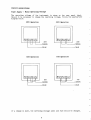
1 . R e m o v et h e B s i d e s c r e w s ( p l u s 2 L o p s c r e w s o n t r i p l e
screws on dual units) notOing the case upper.
units
or 2 handle
2.
Liff
3.
T o r e m o v e a n a i n ( l i n e a r s u p p l y ) p c b , r e m o v e t h e 4 n y J - o nf i - x i n g s c r e w s a n d
remove the J control knobs, which are refalned by grub screws. The pcb can
now be pulled clear of the front panel and the wiring harness allows it to
be rotafed clear of the case l-ower. To remove the logic supply pcb, remove
the 4 MJ screws through the rear panel-.
4.
Transistors Q5, Q6 and Q7 on the linear supplies and Q1, Q2 D10 and SCR1
on the logic supply are insul-ated from the heatsinks.
5.
off
fhe case upper.
Reassembl-e
1n reverse order.
Operating
Voltage
See the Power Supply section on page B for det,ails of changing Lhe operating
volfage of single and dual unlts.
See page 20 for details of changing triple
units.
TECHIIICALSPECIFICATION
Ortput Voltage Setting:
By coarse and fine eontrols;
5mV across the range.
Output Current Setting:
By single
Ortput llode:
The power supply operates in consfant current or
A
constant voltage modes with automafic cross-over.
display annunciator indicates constant current mode.
Output Sritch:
Isolates the output and penmits voltage and current
limits bo be set up before connecbing the load.
Output Ter"ninals:
4mmterminals
Output Inpedance:
Constant Voltage:
Constant Current:
Typically
Typically
resolution
better
than
control.
logarithmic
on 19nn (.75n) spacing.
(5mOhmat lkHz
5OkOhmwith voltage limif
at maximum
Output Protection:
forwardl
Up to maximum output voltage +20 Volts
diode clamped for reverse voltages and up to 3A
reverse cunrent.
Load Regulation:
<0.01$ of maximumoutput for 50X Ioad change
Line Regulation:
<0.01[ of naximum output for
Ripple and Xoise:
Typically
Transient Response:
(2Ousec to
change.
Tenperature Coefficient:
Typica1ly
l{eter Type:
Independent autoranging 0.5''
voltage and current indication.
10[ ]ine
voltage change
(1nV rms
within
5OmV of
setting
for
9Ol' load
(10Oppm/oC
Heter Resolution:
Voltage:
Current:
1 0 n V u p t o 2 0 V , 1 0 0 m Va b o v e 2 0 V
1 m Au p L o 2 A , 1 0 m Aa b o v e 2 A
Heter Accuracy:
Voltage:
Currenf:
0.2% ot reading + 1 digit
0.5fi ot reading + 1 digit
3.5-digit
LCDs for
Power Requirenents:
Input Voltage:
I n t e r n a l l y s e t f o n 1 1 0 , 1 2 0 , 2 2 0 o r 2 4 0 V A C5 0 / 6 0 H 2
Input VoJ.tage Rangez +/' 10ft ot voltage setting
Power Consumption:
1 5 0 V Af o r s i n g l e u n i t s , 3 0 0 V A f o r d u a i u n i t s
hvironnental
Range:
OPerating
Environnental
Penge:
Storage
Size:
Ueight:
5oC to 40oc, 20ft to 80tr RH
-20oC to +60oC
160mnwide x 160mmhigh x 238mn deep single unlt
308nm wide x 160mnhigh x 238mn deep dual unib
4.9kg slngle unit
9.6tg duat unit,
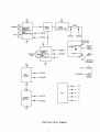
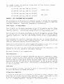
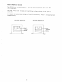
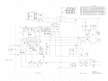
FI]IICTIONAL DESCRIPTION
The relati-onship between the major circuit
diagram opposite.
elements are
showa in
the
block
The pass transistors
are mounted on heatsinks at the rean of the instrunenL.
They are controlled by the emor anplifiens via the diode gate.
The diode gate provides automatic cnoss over of consbant voltage and consfant
current.
In the constant voltage node the error voltage amplifier
constant output voltage, set by the coarse and fine controls,
load; the voltage is sensed across the output terminals.
mainbains the
independent of
In the constant current mode, or when the presef current linit
is neached, the
eurrent error arnplifier overrides the voltage error amplifier
via the diode
gate and mainlains constant output cunrenf independent of load resistance; the
current is sensed across R27.
The output voltage is displayed by the digital
voltmeter.
incorporates the autorange circuitry
and decinal point drive.
This block
also
The digibal
current meter block also incorporates the autonange circuitny,
for the constant current annunicator and control logic which
drive cincultry
allows the set current limit to be displayed.
The powen supply provides high voltage and power for the output
( V 1) .
split low voltage supply for the control circuitry
(V2) and a
-
COARSE
FINE
VOLTAGE
ERROR
IFIER
RENCE
+I
SENSE
-I
SENSE
OUTPUT
SWITCH
o+l
CURRENT
LIMIT
SENSE
CURRENT
ERROR
AMPLIFIER
AND
REFERENCE
I
OUTPUT
TERMINALS
-u2-€l
--€r
+VSENSE
VOLT
METER
_V SENSE
SENSE
-V SENSE
-v1
+v2
+ V'l
-v2
+vl
OV
CURRENT
METER
-v1
Functional
Block
Diagrar
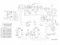
CIRCUIT DESCRIPTIONS
Porer
Supply - llains
Operating
Yoltage
The operating voltage of the instrument is shown on the rear panel labeI.
Should it be necessary to change the operating voltage, foll-ow bhe appropriate
diagran below.
240V Operation
220V @eration
987654321
109876s4321
110V Operation
120V Operation
7654321
If
a change is made, bhe operating
voltage
label
and fuse shoul-d be changed.
If a change
The correct
is made, the operati.ng
fuse type is: -
volEage
1A 250V HRC time-1ag,
20mm for
2A 250V HRC time-laq,
20mm for
2A 250V HRC time-La9,
20rnmfor
4A 250V HRC time-lag,
20mm for
WARNINC I THIS
and
label
fuse
should
220-240V)
)
110-L20V)
single
220-240V)
)
110-120V)
dual
be
changed.
units
units
INSTRT'ITENT }TUST BE E.ARTHED
Any interruption
of the protective
conductor inside or outside
the instrument
or disconnection
of the protective
earEh terminal
is likel,y
to make the
instrument dangerous.
Intentional
interruption
is prohibited.
Power Supply
- DC Requlrementg
Plns 22 and 23 on the mains transformer
provide 34Vrms
of the 30V 2A supplies
of f load and this
is recEif i.ed by the bridge rectif j.er Dl. to D4,' C1 is the
capacitor.
reservoir
The off load voltage across C1 is approximately
45V.
Pins 22 and 23 on the mains transformer
provide
of the 15V 4A supplies
l9Vrms
off load and this is rectified
by the bridge rect.ifier
BRI-; C1 and C25 are the
reservoir
capacitors.
The off
load voltage across CL/C26 is approximately
26V.
R14 discharges
the reservoir
capacitors
when the unit
is turned
load connected;
C5 and R1 form a damping network.
The voltage
reservoir
capacitors
supplies the pass transistors.
Diodes D5 to D8 rectify
wi.th reservoir
capacitors
the centre-tapped
C4 and C5 provide
20V winding
approximately
on pins
+/-13Y.
Regulators
ICl.0 and IC11 with diodes D22 and D23 provide
supplies for the error amplif iers and di.gital met.eri.ng.
The above circuitry
is
on a separate
off with no
across the
18 to
regulated
20 and
+/-5Y6
pcb.
Paee TraneistorE
and must be H (hornetaxial)
types.
Q5 and Q7 are mounted on separate heatsinks
p
a
r
a
l
l
e
l
They are in
and current
sharing is provided by emi-tter resistors
R24
and R25.
Driver transistor
Q5 shares one of the heat.sinks and altogether
Q5,
emitter
fol. l.ower stage.
R23 is on one
of the
Q5 and Q7 make up a darlington
heatsinks and R24, R25, R25 are on the main board;
On 15V 4A units,
R24 and
paEh for C9 when
R25 are on the power supply board.
R25 provides
a discharge
no l-oad is connected.
Diode
Gate
the base of which
Q8 is an emitEer follower,
two error amplif iers via diodes D1,2 and D1,3.
Voltage
Error
is
controlled
by either
of
the
Arplifier
to the positive
output termj-nal;
It should be noted that 0V is referred
to
means that the voltage from the error ampJ.ifier is sma11, sufticient
and overcome resistive
losses.
on the driver
and pass transistors
clockwise pin 2 is
at
when VR2 is fully
IC3a j.s a summing amplifier;
this
turn
0V.
Feedback is from fhe negafive output terminal via R19 to pin 3 where if is
s u m m e dw i f h t h e c u r r e n t f r o m V R ' 1 . F i n e c o n f r o l o f t h e o u t p u t v o l t a g e i s
achieved with VR2 which moves the psuedo ground of IC3a. D11 limits
the
oufput swing of 1C3a below 0V. D10 is a 2.45Y voltage reference which is also
used by fhe voltmeter circuitry.
V R 5 s e t s t h e m a x i m u mo u t p u t v o l t a g e .
Gunenb Bror
lnPlifier
If the preset curnent limit is reached, IC4b overrides fhe voltage error
Output current is sensed by measuring the volt
anplifier via Lhe diode gate.
drop across R27 and bhis is compared to the volLage on bhe wipen of VR3 by
t h e o u t p u t s w i n g o f I C 4 b b e l o w 0 V . V R 8 s e t s m a x i m u mo u t p u t
IC4b. D17 linits
current and VR12 trims the offseb of IC4b so thaf fhe set current limit and
are equal. This is done at low output cunrent levels
the output cunrent linit
(100nDA). D25 is a 2.45V volfage reference which is also used by the current
meter.
Output Sritch
SW2aswitches the +V sense connection between the supply output and the sense
Thls is fo overcone SW2bts contacb neslstance with bhe
terminal ibself.
D15 prevents fhe
oubput on and to malntaln feedback when the oufput is off.
positions.
going
complebely open between switch
feedback loop from
S W 2 bs w i t c h e s t h e s u p p l y o u t p u t f o t h e o u t p u f t e n m i n a l .
Whenthe oufput
rAr is connected fo 0V which signals the
switch is in the ofl posifion,
cument meter to display the set curent limi-t.
Xote: SW2 contacts are gold plated on silven and the correct replacemenf type
Note also that if SW2 is disconnecfed it nust be rewired fhe
must be used.
This is because SW2amust have gold contacLs while the gold
sane way round.
SW2b
conbacts
on
will have been vapourised due to the high switching current
and will have normal silver contacts as a result.
Voltneter
ICl is a standard 3.5 digib panel meter IC.
This is a dual slope A to D
R57 and C14 define the clock frequency of
complete with display drivers,
approximately 40kHz which, if necessary, can be checked using a x10
oscilloscope probe on pin J8. R56 and C12 are the integrator componentsand
C11 the auto zero capacitor.
C13 is the reference capacitor and R58, R59 and
c
o
m
p
o
n
e
n
Ls.
C15 are input filter
R16 and R17 attenuate the output voJ-tage to suit IC1.
The volfmeter autoranges on the 30V 2A supplies between the high and Iow nanges by IC3b
switching fhe meten reference.
The outpuf of the comparafon IC3b is high when
'l
The
the output is below 9V and low when the output voltage is above 19V.
switching point is adjusted by VR4; R5 provides positive feedback whlch gives
Q1 inverts
approxinately +/-0.5Y of hysteresis at the output terminals.
ICl5ts output, providing complementary conLrol signals.
These drive the
analogue switches in IC8 selecting the two refenences for the high and low
ranges. They also select the decimal point via IC9. The decimal point is off
VR7
and on when in anfi-phase.
when in-phase with bhe back-plane signal,
trins the voltmeter on the low range and VR6 trims the high range.
Curent
lleter
The control slgnal rAl
IC2 is the same type as fhat used in the volLmeter.
fron the output switch drives Q10 and IC5b which provides complemenLary drive
signals to ICTa and b. With the output switch on, ICTa eonnects the neter to
R27 to measure output current.
10
ICTb conneets the meter to VR3 to display the
With the output switch off,
currenb tinib setfing.
The currenf meter autonanges on the 15V 4A supplies; VR9 sets the change over
poinb and IC4a selects the appropriate neter referenee.
The output of
conparator IC4a is high when the current reading is below 1.9A and 1ow when
feedback and sone
R41 provides positive
the current reading is above 1.9A.
hysberesis.
l{hen current limit
is reached, IC4b takes controL via the diode gate; a9 is
turned on which enables low frequency osci-llaton IC5c and d which flashes the
triangle in the display.
Note that the ground lead of IC5 ig connected to the
-V1 supply whilst
g
r
ound lead of IC6 is connected bo DGI, whlch is
fhe
generabed by IC2 for the LCD and is between 4 and 6 volts wibh nespecb bo +V1.
Level shifting is provided by R54 and R63.
Protectlon
D16 provi.des protection
against r"everse voltages.
provide protection against forward voltages.
11
D9, D14, Q2, 03 and a4
CILIBRATION
Equipnent
Required
4.5 Oieit nultimeter
voltage and current.
with
10Anp range and better
than 0.1t
aecunacy on both
30V 2l Supplies
Tunn the 3 front panel controls to maximun, output switch
must be fitted between the output and sense tenmi-naIs).
on.
(Shorting
bars
Connecf a voltmefer to the output terminals and adjust VR5 for 30.7V to 30.9V.
Adjust VR6 so bhaL both voltmeters
Reduce the outpub voltage
voltmeters read the same.
to
read the same.
approximately
Set the output to 19V and adjust
'19.6V.
between18.4V and
15V and adjust
VR7 so that
both
the meter auto-ranges at a point
VR4 so that
Conneet an anmeten across the output berminals and adjust
2.OgA.
Reduce the current limif confrol to give approximately
VR10 so bhat both curnent meters read fhe sane.
VR8 to give 2,074 to
1.8A output, and adjust
Set fhe output switch to off, short the output terminals and set the current
linit
control to approximately 100nA on the internal meber. Note the reading,
sef the output switch to on, and adjust VR12 so that the meter sbill reads the
sane.
15V 4A Supplies
Turn the 3 fronb panel controls to naximum, oubput switch on.
must be fitted
between the output and sense ferminals).
Connect a voltmeter to the output tenninals and adjust VR5 for
Adjust VR7 so that both voltneters
bars
15.3V to 15.5V.
read fhe saroe
Connect an ammeter across the output terminals
4 . 15 A .
Adjust VR11 so that
(Shorting
and adjust
Vn8 to give 4.10A to
bofh ammeters nead the same.
Reducethe output current
ammeters read the s€rme.
to approxinately
1.5A and adjust
Set the output current to 1.9A and adjust VR9 so that
nanges at a point between 1.84A and 1.96A.
VR10 so thab both
the current
meter auto-
Set the output switch bo off, short the output terminals and set the current
linit
control to approximately 100mAon the internal meter. Note the neading,
s e f t h e o u t p u L s w i t c h t o o n , a n d a d j u s t V R 1 2s o t h a t t h e n e t e r s t i l l
reads the
s€rme.
12
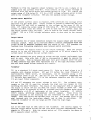
o
VR6
VR7
VR5
o
V R1 2
VR4
PgA @
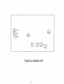
LOCATIONOF CALIBRATIOI POINTS
(VIEI{ED Fnolr co{PolfENTSrOe)
13
TECTINICALSPECIFICATION TS3O23S
See page 5 for specifications
of the main outputs.
LOGIC OUTPUT
Output Voltage Range:
Output Current:
Output Swibch:
Output Terminals:
Over-Voltage Protection:
Output Protection:
Load Regulation:
Li-ne Regulation:
Ripple and lfoise:
Meter T5rpe:
lleter Resolution:
Vollage:
Current:
Heter Aecuracy:
Voltage:
CurrenL:
GE}{ERAL
Power Requirements
Input Voltage:
Power Consumption:
Environmental Operating
Ieight:
1O m V
10mA
0.5% of reading + 1 digit
0.5ft of reading + 1 digit
I n t e r n a l l y s e t f o r 1 1 0 1 1 2 0 1 2 2 0o r 2 4 0 V A C 5 0 / 6 0 H 2 .
I n p u b V o l L a g e R a n g e : + / - 1 0 ' f ro f v o l t a g e s e t f i n g .
300VA
5oc to 4ooc, zo%Lo BotrRH.
Range:
Environnental
Renge:
Size:
4 to 6 Vol-ts
4 Amps minimuml current lirnit approxiamtely 5 Amps.
Isolates the outpuN and permi-fs outpuf voltage to
be set before connecting the load.
4mmterminals on 19mm(.75n) spacing.
2Omsecup to
Dual-speed circuit giving fypically
2
u
s
e
c
a
b
o
v
e
V
V
o
l
t
s
a
n
d
f
y
p
i
c
a
l
l
y
7 olts.
7
Clamped by the over-voltage protection circuif
for
forward volfages over 7 Volts and up to I Amps
f o r w a r d c u r r e n t . D i o d e c J - a m p e df o n r e v e r s e
volLages and up to 3 Ampsrevense current,.
<0.5% for 50ft load change.
<0.5% for 10% line voltage change.
<20mVrms, (50mV pk-pk.
0.5rt 3.5 digit LCDfor voltage or current.
Storage
-20oC to 600 C.
386rrn wide x 160mmhigh x 238mmdeep.
'l
1.0kg
I
tt
ll
j
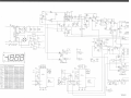
HAINS OPERATINGVOLTAGE
T h e T S 3 0 2 3h a s 3 t r a n s f o r m e r s , z f o r t h e
30v 2A sections and 1 for the
5V 4A section.
See page B for
sections.
fuse ratings
and operating
voltage change of the 30v 2A
To change the operating voltage of the
5V 4A section,
diagram below.
110/120V Operati_on
fo11ow the appropriaLe
220/240V Operati_on
15
CIRCUIT DESCRIPTION5Y 4A
Porer Supply - DC Requirenents
W i t h 2 4 0 V i n p u l , T 1 a n d T 2 o n t h e m a i n s L r a n s f o r n e r p r o v i d e 2 O V r m so n 1 o a d .
T h i s g i v e s a p p r o x i m a t e l y 2 4 V o n C1 .
T 3 a n d T 4 p r o v i d e 1 5 V r m sg i v i n g
10VoutpuL for ICZ.
Sritching
20V on C2,
'Zener
diode D9 gives a regulated
Regulator
The switching regulator
operating aL 25k[z.
is
confj.gured as a step down or
buck regulator
L1 smoobhs the output by storing
Q1 and Q2 form a PNP darlington switch.
enengy when the switch is closed, and supplies energy vj-a D10 when the swifch
R 3 i p r o v i d e s a m i n i m u ml - o a d . L 2 a n d
i s o p e n . C L l1 s t h e r e s e r v o i r c a p a c i t o r .
C5 provide additlonal smoothing.
Regulafion is provided by the control IC, IC1. The reference voltage is
adjusted by VR1 to give an ouLput range of 4V to 6V. This reference is
compared to the voltage on the + sense termlnal and the duty cycle is varled
to fhe switching transistor to maintain regu1atlon.
I f t h e v o l t a g e d r o p a c r o s s t h e c u r r e n t s e n s e r e s i s t o r r e a c h e s 2 0 0 m Vt h e d r i v e
to the switching transisNor is terminafed limiting the output current.
by 100mV,
Shut down of fhe regulator occurs if the outpuf voltage falls
determined by R13 and R14. Q4 is turned off allowing C6 Lo charge up via R34
connected to pin 10 of IC'1. This Lurns the
turning on the transistor
regulator off and the vollage on pin 5 of IC6B fal1s further and results in
Recovery is achieved by Lurning the mains
the power supply being latched off.
supply off for sufficj-ent time for C6 to discharge (approximately 20 seconds).
Frequency compensation for t,he feedback 1s provided by C10, C11
and R12.
Over Voltage
Protection
I C 7 i s a n O V PI C a n d c o m p a r e s t h e v o l t a g e o n p i n 2 w i t h a n i n t e r n a l r e f e r e n c e
(typically
2.6V).
If the voltage on pln 2 exceeds fhe reference, Lhe output
This mode of
d r i v e t o S C R1 i s e n a b l e d a f t e r a d e l a y g e n e r a t e d b y C 3 .
protecflon
functions for output voltages between 6.4V and 7V and takes
fypically 20ms. If the output exceeds 7V, SCRl is fired instantly via pin 5.
to
-
Metering
IC2 i-s a standard DVMIC and is the same type as used in other sections of the
power supply.
With the output switch off, 03 is off turning IC4A off
inverter IC4D, so that the meter reads output volfage.
and IC4B on via
With the output switch on, IC4B is Lurned off and IC4A is tunned on, so fhat
the meter reads output current by measuring the voltage across R7.
VR3 calibrates
t h e m e L e r f o r c u r r e n t m e a s u r e m e n tI i t i s a l s o t h e m e t e n
reference so VR3 must be adjusted before VR2, which calibrates the voltmeter
mode.
and the
O p t o - c o u p l e r I C 3 p r o v i d e s l - e v e l s h i f t i n g b e b w e e nt h e c o n L r o f c i r c u i t r y
the LED inside
LCD drivers.
When the power supply goes into current limit,
IC3 is turned off which turns the phofo-transistor off, enabling 1ow frequency
IC5B and IC5A which flashes the delta sign in lhe display.
oscillator
CALIBRATION
Equipment required:
3.5 dieit
m u l t i m e f e r w i t h a 1 0 A M Pr a n g e .
swilch fhe output
C o n n e c t a 4 A l ' l Pl o a d t o t h e o u t p u t t e r m i n a l s ( 1 R 2 r e s i s t o r ) ,
on and adjust the voLtage control- as necessary to give approxiamtely 4 AI"{PSon
external ammeter. Adjust VR3 so that the meters read the same. VR3 is
located on the display pcb.
Removethe 4A load and connect a voltmefer to the output. Note the reading on
the exfernal- mefer, switch the outpuf off and adjust VR2 so that the meter
reads the same. Switch the output on and off to check the reading on each
meter. VR2 is located on the pcb which is fastened to the rear pane1.
SERVICING IOTES
IC1 nust be a UnitnoderA'Parf.
Q1, D10 and SCRl musf be the specified
parfs.
A temporary short may be put across C6
C4 and C5 are low ESR types.
fo disable the shut down and ease trouble shoofing.
17
PARTS I,TST
PCB AEs€mbly
15v 4A
44115-0060
Reeigtore
Ref
DeecrJ-ptJ.ou
Part
No
R1
R2
R3
R4
R5
R5
R7
R8
R9
R10
R11
R1-2
R13
R14
R15
R15
R17
R18
R19
R20
R21
R22
R23
R24
R25
R26
R27
R28
R29
R30
R31
R32
R33
R34
R35
R35
R37
R38
R39
R40
R41
R42
R43
R48
R49
R50
R51
R52
R53
R54
47RJ W25 CF
10KJ W25 CF
1 . 0 0 K JW 2 5 C F
22KJ W25 CF
Not used
Zero ohm link
Not used
Not used
20K0F W25 MF
750RF W25 MF
550RJ w25 cF
2'7KJ w25 CF
7K50F w25 MF
6K8J w50 cF
10KJ W25 CF
10K0F W25 MF
1M00F w25 MF
Not used
51K0F W25 MF
1K8J W25 CF
47RJ W25 CF
10KJ W25 CF
See Heatsink Assy 2
0 R 33 J 2 w 5 w w
0R33J 2w5 Ww
2K2J W50 CF
0R10J 7w0 ww
10KJ W25 CF
100KJ W25 CF
2M7J Vt25 CF
10KJ W25 cF
1K00F W25 MF
3K90F W25 MF
1K00F W25 MF
9K10F W25 MF
555RF w25 MF
750RF W25 MF
20K0F W25 MF
11K5F W25 MF
7K50F W25 MF
2 M " 7 JW 2 5 M F
NoL used
to
100KJ W25 CF
118KF W25 MF 50ppM
100KJ W25 cF
100KJ w25 cF
1 M 0 0 Fw 2 5 M F
1 M 0 0 FW 2 5 M F
100KJ W25 CF
2 3 L 8 5 - 0 4 ' 70
23185-3100
23L85-4L00
23L85-3220
23185-0000
23202-3200
23202-1750
23185-1550
23L85-3270
23202-2'750
231'79-2580
23185-3100
23202-3100
23202-5100
Ref
Descrlptlon
Part
R55
R56
R57
R58
R59
R50
R51
R52
R53
Not used
100KJ w25 CF
118KF W25 MF
100KJ W25 CF
100KJ w25 CF
100KJ W25 cF
100KJ W25 CF
22KJ W25 CF
180KJ W25 CF
23185-41,00
23202-4118
23185-4100
23185-4100
23185-4100
23185-4100
23L85-3220
231,85-4180
VR4 Not used
VR5
2K2 CermeL
VR6 Not used
VR7
220R Cermet
VR8
1K0 Cermet
VR9
220R Cermet
VR10 220R Cermet
VRLl
2K2 CermeL
VR12 100K CF
23202-3510
23185-2180
2 3 L 8 5 - 0 4 ' 70
23185-3100
No
23319-2220
233'19-1220
233'79-21,00
233'19-L220
23379-1220
233'79-2220
2 3 3 7 7- 4 1 0 0
Capacitore
C1
C2
C3
C4
c5
C5
C7
C8
C9
C10
C11
C]-2
C13
C14
C15
C15
C17
C18
C19
C20
C21.
C22
C23
C24
C25
C26
2 3 2 74 - 0 0 1 0
232'74-0010
23L79-2220
232'7L-0008
23185-3100
23185-4100
23185-5270
23185-3100
23202-2100
23202-2390
23202-21.00
23202-291,0
23202-!655
23202-1750
23202-3200
23202-21L5
23202-2750
23202-5210
23185-4100
23202-4118
23185-4100
23185-4100
23202-5100
23202-5100
23185-4100
1B
4700U 63V
10U 35V
10U 35V
100U 50V
100U 50V
100NM250V
100NK 53V
100NK 63V
100U 53V
100NK 63V
330NK 63V
100NJ 100V
330NK 63V
100PG 63V
330NK 63V
330NK 53V
100NJ 100V
330NK 63V
330NK 63V
100PG 53V
330NK 53V
100NK 63V
100NK 53V
4'7PG 53V
4?Pe 53V
4'700U 63V
Elec
EIec
Elec
Elec
Elec
p/E
p/E
p/E
Elec
p/E
p/E
p/E
p/E
Cer
p/E
p/E
p/E
p/E
p/E
Cer
P/E
p/E
p/E
Cer
Cer
Elec
23555-021,1
2 3 5 5 ' 7- 0 5 4 ' 7
23557-0541
2 3 5 5 1- 0 5 1 0
2 3 5 5 7- 0 5 1 0
23621-0312
23620-0246
23520-0246
23551-0249
23620-0246
23520-022'7
2362A-020'7
23520-022'7
23421-0322
23520-0221
23520-0227
23620-0201
23620-022'7
23520-0227
2 3 4 2 ' 7- 0 3 2 2
23620-0227
23620-0246
23520-0246
2342't-0329
23421-0329
23556-0211
-
SemiconductorE
Ref
D1
D2
D3
D4
D5
D5
D7
D8
D9
D10
D11
DL2
D13
D14
D15
Dl5*
D17
D23
D24
D25
DescrJ,ption
Not used
Not used
Not used
Not used
1N4002
1N4002
1N4002
1N4002
Not used
2N404
l_N4148
1N4148
1N4148
1N4002
1N4002
1N5401
to
1N4148
1N4002
2N404
Part
No
25115-0901
25rt5-0907
25tL5-0907
25115-0907
2 ' 7t 6 L - 0 1 . 2 0
2502L-0901
2502I-090I
2502t-090r
25LL5-0907
251L5-0907
Deecription
Part No
rc1
rc2
IC3
IC4
rc5
rc5
rc1
rc8
rc9
rct_0
rc11
7105RCPL
7105RCPL
TLOT2CP
TLOT2CP
40118E
407088
405588
4 05 5 B E
4 0 70 B E
?8L0sAcP
79L05ACP
2'1L53-0003
27L53-0003
LcD
3.5 Digit
Otber
z / Ivo-ubub
27105-0505
2 12 2 6 - O t L j
2 72 2 6 - 0 70 0
2 72 2 6 - 0 6 5 0
2 72 2 5 - 0 5 5 0
^ l ^ ^ a
A a ^ ^
ztzzo-vtuv
27L60-0oLL
27t60-00t2
LCD
(2) 26]-00-0070
Parte
oD PCB A e e y 1 5 V
Deecri.ption
Part
Zero Ohm Resi.stors
(PCBLinks)
44 off
PCB
2 31 8 5 - 0 0 0 0
35515-1030
25rr7-0020
2502t-0901
251L5-090'7
2 ' 7L 5 t - 0 1 2 0
*DL6 i-s wired across the Red
and Black output termi-nals.
Q1
Q2
Q3
Q4
Q5
Q5
Q'7
Q8
Q9
Ql0
Ref
Z"rX2rA
2534L-021.4
ZTX239/8C549
2 s 3 8 0- 0 2 2 9
Z T X 2 3 9/ 8 C 5 4 9
25380- 0229
Z T X 2 3 9/ 8 C 5 4 9
25380-0229
See Heatsink Assy 2
See Heatsink Assy 2
See Heatsink Assy L
Z T X 2 3 9/ 8 C 5 4 9
2 5 3 8 0- 0 2 2 9
ZTX2!A
2 5 34 t - 0 2 1 4
Z T X 2 3 9/ 8 C 5 4 9
2 5 3 8 0- 0 2 2 9
1g
No
z_
'
ll-Ll | |
PCB Assembly
30v 2A
C i,C
44115-0050
Regletorg
Ref
Deecrlption
Part No
Ref
Descrlption
R1
R2
R3
R4
R5
R5
R7
R8
R9
R1O
R11
R12
R13
R14
R15
R15
R17
R18
R19
R20
R21
R22
R23
R24
R25
R26
R27
R28
R29
R3O
R31
R32
R33
R34
R35
R35
R37
R38
R39
R40
R41
R42
R43
R48
R49
R50
R51
R52
R53
R54
R55
R55
R57
R58
R59
47RJ W25 CF
10KJ W25 CF
100KJ W25 CF
22KJ W25 CF
22MJ W25 CF
5 8 K O FW 2 5 M F
11K5F W25 MF
7K5OFW25 MF
2 O K O FW 2 5 M F
? 5 O R FW 2 5 M F
550RJ W25 CF
56KJ w25 CF
7K50F W25 MF
5K8J W50 CF
1OKJ W25 CF
10K0F W25 MF
1 M O O FW 2 5 M F
470KF W25 MF
1 O O K FW 2 5 M F
1K8J W25 CF
47RJ W25 CF
10KJ W25 CF
See Heatsink Assy 2
0R58J 2W5 WW
0R58J 2W5 WW
2K2J W50 CF
0R10J 7W0 WW
1OKJ W25 CF
1 O O K JW 2 5 C F
2M7J W25 CF
10KJ W25 CF
1 K O O FW 2 5 M F 5 O P P M
9K10F W25 MF
LKSJ W25 CF
Not used
Not used
7 5 O R FW 2 5 M F 5 O P P M
2 O K O FW 2 5 M F 5 O P P M
Not used
Not used
NoL used
Not used
to
100KJ W25 CF
118KF W25 MF 5OPPM
100KJ W25 CF
100KJ W25 CF
1 M 0 0 FW 2 5 M F
1 M O O FW 2 5 M F
100KJ W25 CF
Not used
100KJ W25 CP
118KF W25 MF
100KJ W25 CF
100KJ W25 CF
23L85-0470
23185-3100
23r85-4100
23L85-3220
2322L-0030
23202-3580
23202-3115
2 3 2 0 2 - 2 75 0
23202-3200
2 3 2 0 2 - L 75 0
23r.85-L550
23185-3560
2 3 2 0 2 - 2 75 0
2 3 r ' 79 - 2 6 8 0
23t85-3100
23202-3L00
23202-5100
2 3 2 0 2 -4 4 ' Q
7
23202-4100
23185-2r80
2 3 L 8 5 - 0 4 70
23185-3100
R60
R51
R62
R53
100KJ
100KJ
22KJ
180KJ
VR4
VR5
VR5
VR7
VRg
VR9
VR10
VR11
VR12
W25
W25
W25
W25
Part
No
CF
CF
CF
CF
23185-4L00
2 31 8 5 - 4 L 0 0
23L85-3220
23185-4180
1 O O KC F
2K2 Cermet
2K2 Cermet
220R Cermet
2K2 Cermet
Not used
220R Cermet
Not used
lOOK CF
23377-4100
2 3 3 19 - 2 2 2 0
2 3 3 79 - 2 2 2 0
2 3 3 ' 79 - L 2 2 0
2 3 3 ' 79 - 2 2 2 0
2 3 3 79 - L 2 2 0
2 3 3 ' 7 ' 7- 4 1 0 0
Capacitore
clc2
c3
c4
c5
c5
c7
C8
c9
c10
c11
cI2
c13
c14
c15
c15
CL1
c18
c19
c20
c2L
c22
c23
c24
c25
23284-00t0
23284-00r0
2 3 ) . '97- 2 2 2 0
232'71-0008
2318s-3100
23185-4100
23r85-521 0
23185-3100
23202-2100
23202-2970
23I85-2180
23202-1750
23202-3200
23185-4100
23202-4118
23185-4100
23185-4100
23202-5100
23202-51_00
23185-4100
23185-4100
23202-4118
23185-4100
23185-4100
20
4700u 53v El ec
1 0 u 3 5 v E 1e c
1 0 u 3 5 V EI e c
1 0 0 u 5 0 v E 1e c
100u 50v Elec
1 0 0 N M2 5 0 V P / E
100NK 53V D/tr
1OONK 53V
100u 53v Elec
100NK 53V P/E
330NK 63V P/E
100NJ 100V
33oNK 53V P/E
100PG 63V Cer
33ONK 53V P/E
33ONK 53V
1 O O N Jl O O V P / E
330NK 53V
33oNK 63V P/E
100PG 63V Cer
33oNK 63V
10ONK 63v
10oNK 63V P/tr
47PG 63V Cer
47PG 53V Cer
23555-O2r'7
2 3 5 5 7- 0 5 4 7
23557 -054'7
23551-0510
2 3 5 5 ' 7- 0 5 1 0
2362r-031.2
z56ZV-VZq6
2 3 6 2 0- 0 2 4 5
2 3 5 5 ' 7- 0 2 4 9
23520-0246
2 3 6 2 0- 0 2 2 1
2 3 6 2 0- 0 2 0 7
2 3 6 2 0- 0 2 2 7
2 3 4 2 ' 7- 0 3 2 2
2 3 6 2 0- 0 2 2 1
2 3 5 2 0- 0 2 2 1
2 3 6 2 0- 0 2 0 1
2 3 6 2 0- 0 2 2 ' 7
2 3 6 2 0- 0 2 2 ' 7
2 3 4 2 7- 0 3 2 2
2 3 6 2 0- 0 2 2 7
2 3 6 2 0- 0 2 4 6
2 3 6 2 0- 0 2 4 5
2 3 4 2 7- 0 3 2 9
2 3 4 2 ' 7- 0 3 2 9
other
Semlconductors
Ref
Deecription
1N5401
D1
1N5401
D2
1N5401
D3
D4
1N5401
D5
1N4002
1N4002
D5
D7
1N4002
D8
1N4002
D9
1N4148
D10 2N404
D11 1N4148
1N4148
Dtz
D13 1N4148
D14 1N4002
D15 1N4002
D15* 1N5401
D17 to
D23 1N4148
D24 1N4002
D25 2N404
on PCB Aesy 30V
Part No
Deecriptsion
Part
251.]-1-0020
25t1.7-0020
Zero Ohm Resistors
(PCBLinks)
44 off
PCB
23185-0000
35515-0950
z5Lr/-vuzv
2511.1-0020
25tI5-0901
25tL5-0907
25t15-090'7
25115-090?
2502t-0901_
27151,-01.20
2502r-090t
2502t-090t
2502!-090L
25115-0907
25115-0907
25L17-0020
2502L-090t
25715-0901
21L51,-01.20
*D1,5 is
wired across the Red
and Black output terminals.
Q1
Q2
Q3
Q4
Q5
Q5
Q'7
Q8
Q9
Q10
2534L-0214
ZTX2I4
2 5 3 8 0- 0 2 2 9
Z T X 2 3 9/ 8 C 5 4 9
Z T X 2 3 9/ 8 C 5 4 9
2 5 3 8 0- 0 2 2 9
2 5 3 8 0- 0 2 2 9
ZTX239/8C549
See Heatsink Assy 2
.)
See Heatsink Assy
See Heatsink Assy 1
25380-0229
Z T X 2 3 9/ 8 C 5 4 9
2534I-0214
ZTX2I4
Z T X 2 3 9/ 8 C 5 4 9
2 5 3 8 0- 0 2 2 9
IC1
rc2
IC3
IC4
rc5
IC5
IC?
rc8
IC9
ICl.O
IC11
7 1 . 06 R C P L
7105RCPL
T L O ' ]2 C P
TLOT2CP
4 01 1 B E
407OBE
4O55BE
4055BE
407OBE
78LO5ACP
79LO5ACP
LcD 3.5 Disit
Parta
No
Rear Mounted Heatelak Aseye
for all S gerLee PSUg
Note: 30V Single, Dual & Trj-ple
Heatsink Assys,
PSUs use identical
The 15V 4A PSU Heatsink Assys
use the same components but are
wired differentlv.
Heateink Aeeenbly
consistinq of:
1
Deecription
Part, No
Heatsink type 1
2N30ssH (07)
Mount
Translstor
Mica Washer
Screw M3 x 12mml- 2 off
Washer M3
2 off
Solder tag M3
2 off
Nut M3
2 0 5 ' 7 0 - 0 0 9 0( * )
25385-0010
20611-0007
205r3-0010
20234-0025
20030-0253
2245r-0203
20210-0101
Heatelnk Aseenbly
consist j.ng of :
2
Deecription
Parts No
Heatsink TVne 2
2N3055H
(Q5, Q5)
Transistor Mount
Mica Washer
Screw M3 x 12mml
Washer M3
Solder tag M3
Nut M3
4 7 R J W 2 5 C F ( R 2 3)
20670-0100 (*)
2'7L53-0003
21L53-0003
2"7L06-0606
27L05-0605
2 ' 72 2 5 - 0 1 L 0
2 ' 72 2 6 - 0 ' 70 0
2 72 2 6- 0 5 5 0
2 ' 72 2 6 - 0 5 6 0
2 7 2 2 6 - 0 ' 70 o
27160-0011 (*) See manufacturing
page 25.
27150-00L2
LCD (2) 25100-0070
2L
2
2
2
4
2
2
4
off
off
off
off
off
off
off
25385-0010
20611-0007
205L3-0010
20234-0025
20030-0253
22451-0203
20210-01-012 3 1 - 8 5 - 0 4 '0t
changes on
Loglc
PCB Aeeenbly
of :
conel.eting
Supply
44115-0070
Capacitore
ReeleEore
Ref
Deecription
RL
R2
R3
R4
R5
R5
R7
R8
R9
R10
R11
R12
R13
R14
R15
R15
R17
R18
R19
R20
R21
R22
R23
R24
R25
R25
R2'7
R28
R29
R3O
R31
R32
R33
R34
R35
R35
R37
R38
R39
1K0J W25 CF
1 O R O FW 5 O M F
1 O R O FW 5 O M F
100RJ W25 CF
8 2 O R FW 5 O M F
8 2 O R FW 5 O M F
O R O 3 3 J4 W M R
1K59F W25 MF
IK].OF W25 MF
1K59F W25 MF
2K2J W25 C?
52KJ W25 CF
3K90F W25 MF
200KJ W25 CF
200RF W25 MF
2 O O R FW 2 5 M F
3 K 5 O FW 2 5 M F
3K90F W25 MF
35K0F W25 MF
3K90F W25 MF
100KJ W25 CF
1L8KF W25 MF
100KJ W25 CF
100KJ W25 CF
1M0J W25 CF
1M0J W25 CF
1M0J W25 CF
1MOJW25 CF
1 M O FW 2 5 M F
1 M O FW 2 5 M F
2 O O R FW 2 5 M F
1 O O R JW 2 5 C F
4?RJ W25 CF
36K0F W25 MF
100RJ W25 CF
35K0F W25 MF
5K81F W25 MF
3K90F W25 MF
1K0J W25 CF
Vt(I
POC
VRz
VR3
PS/H 100R Cermet
PS/H 2K2 Cermet
IUK
IJlN
Part No
Ref
23285-2L00
23226-0)-00
23205-0t00
23185-1100
23205-t820
z5zuo-
(continued)
1000U 10V
100U 25V
100NK 53V
100NK 53V
10NJ 400V
4N7K 100V
100PG 53V
10oNK 53V
33oNK 53V
330NK 53V
100PG 53V
330NK 53V
33oNK 63V
330NK 63V
100NK 63V
100NK 63V
10ONS 63V
C22 1N0Z 500V
c23 100NK 53V
C24 10NZ 63V
C5
C5
c7
c8
c9
c10
C11
c12
c1.3
c14
c15
c15
cl,7
c18
c19
c20
*C21
rdzv
2 3 2 7L - 0 0 0 9
zJzvz-zLo>
23202-211,0
23202-2]-69
23L85-2220
23L87-3520
23202-2390
23187-4200
23202-1200
23202-t200
23202-2350
23202-2390
23202-3360
23202-2390
2318s-4100
23202-4118
23185-4100
23185-4100
23185-5100
23185-5100
23185-5100
23185-5100
23202-s100
23202-5100
23202-1200
23185-1100
23L85-04'70
23202-3350
23185-1100
2 3 2 0 2 - 3 36 0
23202-268t
23202-2390
23L85-2L00
Part
Deecription
Low ESR
EIec
P/E
P/E
P/E
P/E
Cer
P/E
P/E
P/E
Cer
P/E
P/E
P/E
P/E
P/E
Cer
Cer
P/E
Cer
*Note C21 is fitted
output terminal-s
No
23551-0810
2355'l-0550
2 35 2 0 - 0 2 4 5
2 3 5 2 0- 0 2 4 6
2352L-03L0
2 3 5 2 0- 0 2 4 5
2 3 4 2 7- 0 3 2 2
2 3 6 2 0- 0 2 4 6
2 3 5 2 0- 0 2 2 7
2 3 6 2 0- 0 2 2 7
2 3 4 2 7- 0 3 2 2
z36ZU-VZZ
/
23520 -022'7
2 3 6 2 0- 0 2 2 7
2 3 6 2 0- 0 2 4 6
2 3 6 2 0- 0 2 4 6
23438-000'7
23424-0445
2 3 6 2 0- 0 2 4 5
23427-0325
across the
Semlconductorg
Ref
Deacriptlon
Part
D1
D2
D3
D4
D5
D5
D7
D8
D9
*D1,0
1 N 5 40 1
1N5401
1 N 5 4 01
1 N 5 40 1
1N4002
1 N 40 0 2
1N4002
1 N 40 0 2
10V Zener
10TQ030
1 N 40 0 2
1N4002
1N4148
1N4148
1N4148
6V2 Zener
25rr1-0020
25rr'7-0020
25II1-0020
25LL7-0020
25Lt5-0907
25115-0907
25L75-0907
25rr5-090'7
2 5 1 , 3 0- 0 2 3 9
25775-07 t0
25]-]-5-090'7
251,r5-09 0'7
2502L-0901
2502r-0901
2502I-0901
25r)0 -0220
Q3
Q4
BDT92
8D234
ZTX214
Z " r X 2 3 9/ 8 C 5 4 9
25334-0072
25334-0009
2534r-0214
2 5 3 8 0- 0 2 2 9
*SCR
8T151-5OOR
25210-0010
*Note
D10, Q1,Q2, SCR are
Heatsrnk Assy on
D11
Dr2
D13
DI4
D15
D15
23347-0130
23319-1100
2 3 3 19 - 2 2 2 0
No
Capacitore
Ref
C]C2
C3
C4
Description
3300U
100U
1U0
1000U
40V
25V
53V
10V
Elec
Elec
Elec
Low ESR
Part
"Q1
*Q2
No
23556-02L8
23551-0550
23557-0509
23557-0810
the
22
fitted
PCB
to
Semlconductors
(contlnued)
Ref
Deecrlption
Part
IC1
U C 35 2 4 A N
7 105RCPL
c M v 1 7- 3
2'7160-0310
2'7153-0003
2'7001-0020
2 72 2 5 - 0 5 6 0
2 7 2 2 5 - 0 ' 70 0
2 7] , 0 5 - 0 5 t 3
2 1L 0 2 - 0 0 t 0
rc2
rc3
aaA
IC7
40558
40708
L M 35 8
M C 34 2 3 P l _
LCD
3 .5 Digit
Other
Part,g on Loglc
1Lf
LL
o
Deecrlptlon
LCD
No
26LOO-00?0
Supply
PCB ABsy
Part
No
Heatsink
3I5I2-03 10
Washer (SIL-PAD)
4 off 205L3-0005
Bush, TO220
3 off 20511-0003
Screw M3 x 10mmL 4 off 20234-00L1
Washer M3
4 off 20030-0263
Washer M3 s/proof
5 o f f 2 0 0 3 ' 7- 0 3 0 1
Stud M3 x SmmL
(for heatsink)
2 off 20205-0500
Screw M4 x 30mml cheese head nylon
( f o r L l -)
20224-02L0
Nut M4 nylon (for L1)
20210-0201
15 Pin IC Socket
2 2 5 ' 74 - 0 1 2 0
14 Pin IC Socket
2 off 22574-0119
8 Pin IC Socket
2 off 22574-0118
Zero ohm resistor
14 off 23185-0000
Fuse Clj.ps
2 off 22312-0240
Fuse 5 Amp A/S Fs2
22315-0231
Inductor 20OuH 4A L1
22154-0010
rnducror 2.2uH
L2
22042-0100
Inductor 7 T\-rrns
L3
2 2 1 5 2- 0 0 1 0
rnducror 5.8uH
L4
22042-0110
PCB
35515-1040
Connector Aeey 16 Vilay Inter
consisting of:
PCB
Cable 15 Way IDC Flat
7.5 ins off 10148-0001
Connector transition
15 Way
2 of f 22515-004'7
23
Parts
Comnon to
Deecriptlon
; a-
all
Parts
PSUg
Part
No
C1ip, capacitor for C1 20555-0520
Switch, rocker SW1
22219-0100 (*)
switch, rocker 5W2,3,4 222L9-0110 (*)
22300-O2LO (*)
Fuseholder
Shroud for fusehoLder
22458-000t
2 0 5 5 1- 0 0 0 2
Knob, black
Cap, black for knob
2 0 6 5 7- 0 0 0 9
Pot, 1K0 li-n, VR1
23348-0060b
VR2
Pot, 1K0 lin,
23348-0020
Pot, 10K 1og, VR3
23348-0030
Terminal, Red
225'1I-05?0
Terminal, Black
2257).-0680
Terminal, Green
225'71-0690
Shorting bar
(output terminaLs)
35331-0080
BezeL for displays
3l'7LI-0020
Solder tag 4BA
(output terminals |
22451-0200
Washer 4BA shakeproof
(ouEput termj-nals)
2 0 0 3 1- 0 2 4 1
Diode 1N5401 (D15;
(output terminals)
25L1,'7-0020
Bracket,switch
support
31512-0270
for SW1,2,3
Washer M3
(Heatsink to
rear panel etc )
20030-0253
Grommet 3109A black
(for heatsink wiring)
22443-0002
Foot
20662-0510
SoLder tag, s/prf 6BA
(Earth wire to
earth tag)
2003'7-0400
Screw No 5 x 3/8"1 Self tap
(C1, Case and Feet
securingl
20052-0700
Self tap
Screw No 5 x I/2"I
(Transformer securing)
20652-0710
Captive Nut
(Transformer,
CI,
and Case securing)
20213-0010
S c r e w M 3 x S m m LN y l o n
(PCB to front panel and Heatsink
cover to spacers
20224-0200
Screw M5 x 5mml,
(Earth Lag to
lower case)
20234-0017
Cable tie for wirr-ng
20653-0204
Spacer M3 x 30mml
Hex studded
(Heatsink mounting)
2065I-0235
spacer M3 x 30mm
round clearance
(Heatsink mounting)
20661-0243
(*)
Screw M3 x 40mml
(Heatsi-nk (cover) )
20234-A038
Comlon (continued)
Deecriptlon
Part
Bush, strain rel-ref
(for mains cable)
Mains cabLe
cut from
Label, wiring
i-nstructions
Mains lead wi-th
Euro plug
Mains lead with
USA plug
Handle
Serial No label
End caps for carton
Guarantee card
Tnstruction Book
No
22448-0220
10175-0110
37541-0490
2249L-0200
22491.-02L0
292L1-0110
37522-0150
20554-01-90
48581-0230
48511-0050
Additional
P a r t g C o r u n o nt o
and 30V Single PSUe
15V
Deecrlption
Part
Case, upper
Case, lower
Warning Label
Warning Label
Warning Label
Warning Label
Carton
33535-0630
33535-0700 (*)
37559-0100
3 1 5 5 9- 0 1 1 0
37559-0120
37559-0130
38114-01-30
-
240v
220V
720v
110V
No
Additional
Parte Coruron to 15V
and 30V Single & Dual PSUe
Deecription
Part
Cover, heatsink
31512-0130 (*)
Additional
Partse comlon to
Dual and Triple
PSUg
No
30V
Deecription
Part
Bracket,
Warning
Warning
Warning
Warning
33111-0180
37559-0140
3'7559-0150
37559-0160
3'7559-0170
handle/case
label - 240V
label - 220V
label - I20V
label - 110V
No
AddiElonal Parts comnon to 30V
Sing1e, Dual & TripJ.e PSUg
DeEcription
Transformer
Part
30V
See manufacturing
page 26.
24
No
22715-0070
changes on
Additional
Partse unigue
to
15V PSU
Description
DeecripEion
Part
Facepl-ate
Ceramic beads
for R24,25
Bridge Rectifier
Push-on Tags for
Transformer
33331-1320 (*)
Additional
Partg
No
unique
to 30V
single
PSU
(*)
ParE No
Faceplate
33331-1310 (*)
Parte
unique
Part. No
33331-1110 (*)
33535-0650
33536-0710 (*)
38114-0r40
F:
e an
C:
<a
Ca
qo
l :
l- o
l lnnar
I ar^ror
Carton
Additional
Parts
to
Triple
Description
Part
No
Faceplate
Case, upper
Case, Iower
Cover, Heatsinks
Cover, HeaLsi-nks
Screw M4 x 6mml,
(for case brackets)
Screw M3 x SmmL
(for case brackets)
Bracket, switch support
(for SW4)
Res 84K5F W25 CF
( R 1 0 1'
33331-1390 (")
33535-0720
33535-0730 (*)
3I5I2-0230 (*)
3151.2-0310
1 0K
Trimnof
unigue
(Logic
PSU
20234-0034
20234-0012
3L512-0290
23202-3845
Ccrmet
(vR101)
Snar-erq
See manufacturing
page 26.
to 30V
Dual PsU
Deecriptiou
23319-3100
Hev M? v
Supply
30mml
PCB to
Part
No
1A Anti surge HRC
(for 220/240V Single PSUs) 22315-9501,
2A Anti surge HRC
(for 1I0/720V Single PSUs
and 220/240V Dual & Trj-ple PSUs)
2231,5-9502
4A Antj. surge HRC
(for 110/120V Dual & Triple
PSUs)
22315-9503
22482-0010
252L1-0300
22454-004L
221L5-0090
BR1
BR1
Descrigtlon
Additional
Fueee
Case)
2066r-0241
Logrc Supply
22II5-0100
Aftachmenf nArfs for transformer
Screw M4 x 5mml,
20234-0028
Washer M4
20030-0266
Washers/proof M4
20031-0304
Nut M4
20210-0102
Transformer,
25
changres on
MANI'FACTURTNG CIIANEES
From mid-91 new switches (both AC mains and DC output) and fuseholder were
changes to alI chassis, faceplate and heatsrnk
introduced, necessitating
covers. At the same time the heatsink mounting holes in the chassis were
changed to accommodate a standard pre-drilled
heatsink.
Early and new parts
are noL interchangable;
switches and fuseholders are availabLe
the earlier
Fq
qntraq
TThi f <
can be easily identified
are mounted on a small pcb. The new part
rr< i nn
terminals
Fha
nar.r
h:rl-<
Original
Description
Heatsink
type
1
lloa|-qink
frrno
?
Spacer
Spacer
Bushes
Switch,
Switch,
2Q5'70-0090
205'70-0100
2066L-0236
20667-0243
(HeaLsinks)
(Heacsinks)
(Heatsinks)
rocker
rocker
Fuseholder
SW1
5W2,3,4
Qinala
aha<<ic
Single
heatsink
cover
Faceplate
Faceplate
TS15415
TS302LS
FacepJ-ate TS3022S
Dual- chassis
Faceplate
TS3023S
m-;*1^
r! rPre
^L-^^i
!tla>>I>
Trinle
heal-sink
Additional
^
Parte
ParE
cover
22219-0100
22219-0110r
22300-0210
33535-0700
31,5]-2-0130
33331-1320
33331-1310
33331-1110
3 3 5 35 - 0 7 1 0
33331-1390
33536-0730
31512-0230
because the DC output
numbers are as follows:
N€w Part
20670-9001
206'70-9001
2066r-0242
20557-9302
206]-L-9305
22219-0050
I
- 2 2 2 1 9 - 0 0 8 0- r
22300-9301
33535-0900
375]-2-03'7 0
33331-1740
33331-1730
33331-1390
33535-0910
33331-1760
33535-0920
31572-0340
(Per each output)
PCB (terminals)
Screw 4BA (terminals)
Spacer 4BA (term:-naIs )
W a s h e r ( g r e e n e a r t h t e r m j . n aI )
35515-1210
20134-9005
20661_-Q257
2257r-0591
26