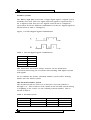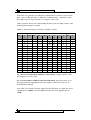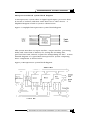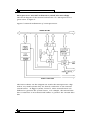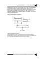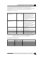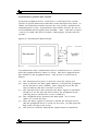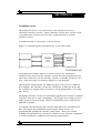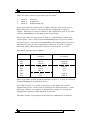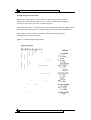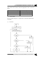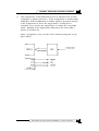
1
STAFF INFORMATION AND SUPPORT MATERIAL
SECTION S1
Outcomes to be covered in the unit
Outcome 1
Describe a microprocessor-based system.
Performance criteria
(a) Given the block diagram of a microprocessor-based system, the
function of each block is clearly described.
(b) Describe the internal architecture of a microprocessor.
(c) Semiconductor memory, memory organisation and memory
decoding techniques used in microprocessor systems, are clearly
explained.
(d) The basic instruction cycle and system bus functions are clearly
explained.
Note on the range of the outcome
Microprocessor-based system: memory devices, microprocessor, input/
output interface, address, control and data bus interconnections.
Memory: dynamic random access memory (DRAM), static random access
memory (SRAM), programmable read only memory (PROM), video
random access memory (VRAM), cache memory.
Memory organisation: system memory map, memory and dedicated
input/output.
Evidence requirements
Written and graphical evidence that the candidate can correctly describe
the function of each part of a microprocessor-based system in terms of
semiconductor memory, memory organisation, memory decoding, the
instruction cycle and system bus.
Outcome 2
Explain methods of input and output data transfer.
Performance criteria
(a) Parallel data transfer techniques are clearly explained.
(b) The technique of interrupts to synchronise data transfer is clearly
explained.
(c) The operation of a non-maskable interrupt (NMI) as a technique
for determining the priority of an interrupting device is clearly
explained.
MICROPROCESSOR SYSTEMS HARDWARE (AH ELECTRONICS)
1
STAFF INFORMATION AND SUPPORT MATERIAL
Note on the range of the outcome
Data transfer techniques: synchronous, asynchronous (handshaking).
Evidence requirements
Written and graphical evidence that the candidate can correctly explain
parallel methods of data transfer and the technique of interrupting in
data transfer.
Outcome 3
Use a programmable peripheral interface integrated circuit.
Performance criteria
(a) Given the block diagram of a programmable peripheral interface
(PPI) integrated circuit, its operation is clearly explained.
(b) Using a manufacturer’s data sheets, a programmable peripheral
interface integrated circuit configuration is designed to meet a
given specification.
(c) Given suitable software and hardware, a programmable peripheral
interface integrated circuit is configured and tested to meet a
desired specification.
Note on the range of the outcome
The range for this outcome is fully expressed in the performance
criteria.
Evidence requirements
Written and graphical evidence that the candidate can explain the
operation of a programmable parallel interface integrated circuit.
Performance evidence that the candidate programmes and tests a
programmable parallel interface integrated circuit.
Outcome 4
Modify an assembly language program.
Performance criteria
(a) A given functional assembly language program is analysed and its
operation is clearly explained.
(b) A specified operational change for the assembly language program
is correctly designed.
(c) The specified operational change for the assembly language
program is implemented and tested until fully functional.
2
MICROPROCESSOR SYSTEMS HARDWARE (AH ELECTRONICS)
STAFF INFORMATION AND SUPPORT MATERIAL
Note on the range of the outcome
The range for this outcome is fully expressed in the performance
criteria.
Evidence requirements
Written and graphical evidence that the candidate can explain and
modify a given assembly language program.
Performance evidence that the candidate can implement and test a
specified modification to an assembly language program until it is
functional.
MICROPROCESSOR SYSTEMS HARDWARE (AH ELECTRONICS)
3
STAFF INFORMATION AND SUPPORT MATERIAL
SECTION S2
Teaching and learning advice; including how to use the
resource material
Teaching methods
In general the teaching and learning methods used are very dependent
on the contents of the unit and the facilities and expertise available at
the delivering centre. By their very nature, however, the units in the
Advanced Higher Electronics course suggest the following teaching
methods:
• laboratory-based learning activities
• use of demonstration circuits where possible
• use candidate-centred circuit testing and analysis
• relate essential theory to circuit applications
• place components used in commercial contexts
• use worked examples to illustrate software structures
• use input/output data transfer demonstrations with prepared software
• refer to manufacturers’ data sheets for devices under investigation.
It is important that all the teachers/lecturers working on the Advanced
Higher Electronics course share a commitment to these methods and
employ them as much as possible. In addition, other methods may be
identified – such as Computer Based Training if the centre has such a
facility. The outcome of this should be a teaching methodology that
pervades the course and sets it apart from others.
4
MICROPROCESSOR SYSTEMS HARDWARE (AH ELECTRONICS)
STAFF INFORMATION AND SUPPORT MATERIAL
Microprocessor Systems Hardware unit delivery
Main topics
Outcome 1
Microprocessor-based system block
diagram
Delivery suggested
Semiconductor memories
Explain the theory and technology,
tutorial examples
Memory organisation
Explain the theory, supplement with
examples
Internal architecture of a
microprocessor
Describe the generalised 8-bit
architecture and relate it to a 16-bit
microprocessor, e.g. Intel 8086
Instruction cycle
Explain theory of a fetch execute cycle
Outcome 2
Synchronous and asynchronous
data transfers
Explain the theory, tutorial examples.
Practical exercises
Explain the theory and technology,
tutorial examples
Maskable and non-maskable
interrupts
Explain the theory, tutorial examples
Priority of interrupts
Explain the theory, tutorial examples
Outcome 3
Programmable peripheral interface
(PPI) chip and its control register
Literature searches, data sheets, explain
technology, benefits and use
Simple assembly language programs
Explain theory, practical exercises
Input/output data transfer programs
Explain theory, practical exercises
Outcome 4
Microprocessor instruction sub-set
Explain the main types of instructions
Basic programs
Explain the operation of simple programs
that use the instructions, such as ADC,
OR, and SHL
Advanced programs
Explain the operation of complex
programs that use masking and input/
output instructions
MICROPROCESSOR SYSTEMS HARDWARE (AH ELECTRONICS)
5
STAFF INFORMATION AND SUPPORT MATERIAL
SECTION S3
Details of starting points based on Higher Electronics
The units in Higher Electronics have been reviewed below for starting
points for the teaching of topics in Microprocessor Systems Hardware
(AH). Relevant outcomes are identified using the Microprocessor
Systems Hardware (AH) outcomes as the basis.
Outcome 1
Describe a microprocessor-based system.
The main topics are microprocessor-based systems, microprocessor
internal block diagram, semiconductor memory, memory map and
instruction cycle.
Unit
Starting point
Power Supplies (H)
None
Signal Processing and Noise (H) Types of signals. Description of a
Analogue and Digital
digital signal.
8-bit devices and the notion of bytes
Interfacing (H)
Electronics Case Study (H)
and busses.
None
Outcome 2
Explain methods of input and output data transfer.
The main topics are synchronous and asynchronous data transfers,
maskable and non-maskable interrupts, and the priority of an interrupt.
Unit
Starting point
Power Supplies (H)
None
Signal Processing and Noise (H) None
Analogue and Digital
Interfacing (H)
Data communication techniques
Electronics Case Study (H)
None
6
MICROPROCESSOR SYSTEMS HARDWARE (AH ELECTRONICS)
STAFF INFORMATION AND SUPPORT MATERIAL
Outcome 3
Use a programmable peripheral interface integrated circuit.
The main topics are PPI block diagram, PPI mode of operation, control
byte and testing the operation of the device in different configurations.
Unit
Starting point
Power Supplies (H)
None
Signal Processing and Noise (H) None
Analogue and Digital Interfacing (H) Data communication techniques.
Parallel data transfers.
Electronics Case Study (H)
None
Outcome 4
Modify an assembly language program.
The main topics are microprocessor instruction sub-set, simple
programs (based on processes), and complex programs (based on
decisions, masking, and input/output instructions).
Unit
Power Supplies (H)
Starting point
None
Signal Processing and Noise (H) None
Analogue and Digital
Interfacing (H)
Electronics Case Study (H)
None
None
MICROPROCESSOR SYSTEMS HARDWARE (AH ELECTRONICS)
7
STAFF INFORMATION AND SUPPORT MATERIAL
SECTION S4
Assessment procedures showing what is to be assessed,
when it is to be assessed, and methods of recording results
Using the instruments of assessment
The Microprocessor Systems Hardware unit is assessed using only five
instruments of assessment. Two class tests, one written assignment and
two laboratory reports assess all of the performance criteria. The
laboratory assignments include test questions that ensure all
performance criteria are assessed.
The following table shows how assessment tasks are related to their
outcome and performance criteria. It also lists the evidence that should
be collected.
Outcome
PC
Assessment task
1
a)
b)
d)
Outcome 1 test paper comprising
structured questions on the microprocessor block diagram, internal
architecture and fetch/execute cycle.
Outcome 1 written assignment covering
semiconductor memories, memory map,
address decoding and I/O addressing.
Outcome 2 test paper with structured
questions on parallel data transfer
techniques, interrupts and priority of
interrupts.
Outcome 3 laboratory assignment
questions to correctly explain the
operation of a PPI chip.
Outcome 3 laboratory assignment to
configure and test the operation of the
PPI device to meet a given specification.
Outcome 4 laboratory assignment questions
to correctly explain the operation of a
functional assembly language program.
Outcome 4 laboratory assignment to
modify and test an assembly language
program to meet a specified operational
change.
c)
2
a)
b)
c)
3
a)
b)
c)
4
a)
b)
c)
8
MICROPROCESSOR SYSTEMS HARDWARE (AH ELECTRONICS)
Evidence to be
collected
Completed test
sheets
Completed
assignment
sheets
Completed test
sheets
Completed
laboratory
assignment sheets
Completed
laboratory
assignment sheets
Completed
laboratory
assignment sheets
Completed
laboratory
assignment sheets
STAFF INFORMATION AND SUPPORT MATERIAL
The timing and duration of assessments
It is recommended that the microprocessor systems hardware be taught
as a sequence of ‘blocks’, with a theory block followed by a practical
block. At the end of each block there should be an assignment that
concludes the work on the block while providing evidence for the
performance criteria. The timing of these assignments is dependent on
the candidate’s understanding of the relevant block; these should be
selected with that as the main constraint.
The recommended sequence for teaching the unit as follows: outcomes
1, 3, 2, and 4.
Outcome 1 assessment is in two parts. The first part is a written class
test, which should be delivered after the teaching of the whole of
Outcome 1. The second part is a written assignment covering PC (c),
which should be given after the teaching of this topic. As an integral
part of the teaching candidates should be given opportunities to attempt
questions on the microprocessor-based system and memory
implementation similar to those likely to be encountered in the end-oftopic assignment and test. This will reinforce teaching while preparing
the candidate for assessment. The class test involves the completion of a
pro forma and should be allocated about 90 minutes. The memory
implementation assignment should be returned within one week of
issue and it should be an integrated learning and assessment activity
with emphasis clearly on learning while assessment evidence is
generated as a natural by-product.
Outcome 2 assessment is a class test on data transfer techniques, which
should be delivered after the teaching of that topic. As an integral part
of the teaching, candidates should be given opportunities to attempt
questions on data transfer techniques similar to those likely to be
encountered in the end-of-topic assignment and test. This will reinforce
teaching while preparing the candidate for assessment. The class test
involves the completion of a pro forma and should be allocated about 60
minutes.
Outcome 3 assessment, a laboratory assignment on the programmable
peripheral interface (PPI), should be delivered after the teaching of that
topic. As an integral part of the teaching candidates should be given
opportunities to attempt questions on PPI configuration similar to those
likely to be encountered in the end-of-topic laboratory assignment. This
will reinforce teaching while preparing the candidate for assessment. All
candidates must test the operation of the PPI in different modes using
MICROPROCESSOR SYSTEMS HARDWARE (AH ELECTRONICS)
9
STAFF INFORMATION AND SUPPORT MATERIAL
prepared software. The laboratory exercise should be allocated about
120 minutes including the completion of a pro forma report. This
should be an integrated learning and assessment activity with emphasis
clearly on learning, while assessment evidence is generated as a natural
by-product.
Outcome 4 assessment is a laboratory assignment on assembly language
programming, which should be delivered after the teaching of that
topic. As an integral part of the teaching candidates should be given
opportunities to analyse and modify pre-written programs similar to
those likely to be encountered in the end-of-topic laboratory
assignment. This will reinforce teaching while preparing the candidate
for assessment. All candidates must explain prepared software. Modify
and test until fully functional, the change applied to the given program.
The laboratory exercise should be allocated about 120 minutes including
the completion of a pro forma report. This should be an integrated
learning and assessment activity with emphasis clearly on learning, while
assessment evidence is generated as a natural by-product.
In principle, there are no time limits for the completion of the
instruments of assessment, but it is likely that a maximum time will be
allocated for the completion of each assignment. It is expected,
however, that the average candidate will complete the work within the
maximum time allowed. The table below indicates the recommended
time allocated for each instrument of assessment.
Outcome
1
Suggested time
90 minutes (PCs a, b, d)
2
3
60 minutes
120 minutes
4
120 minutes
It should be noted that the assessment instruments for outcomes 3 and
4 are practical laboratory assignments. These assignments should be an
integral part of the learning process used to develop the candidate’s
knowledge, understanding and experience of the technology. They
should produce assessment evidence that the candidate has reached a
satisfactory achievement level as a result of the teaching and learning
process.
10
MICROPROCESSOR SYSTEMS HARDWARE (AH ELECTRONICS)
STAFF INFORMATION AND SUPPORT MATERIAL
Reassessment
Time is allowed within units for the assessment and reassessment of
outcomes. Where a candidate has not attained the standard necessary
to pass a particular outcome or outcomes, there should be an
opportunity to be reassessed. Reassessment should focus on the
outcome(s) concerned and, as a general rule, should be offered on a
maximum of two occasions following further work on areas of difficulty.
Evidence from the original unit assessment should assist teachers and
lecturers to identify why an individual candidate has failed to achieve a
particular outcome and to plan focused support for learning.
For all the outcomes the reassessment should be based on the original
instrument of assessment.
When candidates have not produced a satisfactory answer to a section of
an assessment they should only be asked to repeat those sections in
which they have not provided suitable responses. Candidates should be
asked to complete the reassessment under the original controlled
conditions. This reassessment should take place as soon as practicable
after the initial assessment and after discussion and analysis of the initial
assessment has taken place between the candidate and the assessor.
Candidates should be informed of the sections of the assessments that
they are required to repeat and given additional teaching to help them
tackle the reassessment. When there is a substantial number of
candidates requiring reassessment a revision lesson on the problem area
should be presented before reassessment.
Candidates may produce an answer that is substantially correct but
contains minor errors such as the mislabelling of a diagram or the
incorrect reading of an instrument (1011 0011 being C3H instead of
B3H). In this situation, candidates should be reassessed by asking them
to give the correct answer orally. This should take place as soon as
possible after the initial assessment and before any fuller discussion or
analysis of it.
In the laboratory it is important that the focus is on microprocessor
technology, data transfer and assembly language programming and that
other issues such as the use of computers and the installation of
hardware (interface and application cards) do not distract the
candidate’s attention. To this end candidates attempting this unit
should be familiar with any test equipment or system software used and
be able to debug, compile and verify programs. The assessor should
distinguish between assessment difficulties resulting from a candidate’s
MICROPROCESSOR SYSTEMS HARDWARE (AH ELECTRONICS)
11
STAFF INFORMATION AND SUPPORT MATERIAL
weakness in the use of test equipment or system software and a lack of
understanding of microprocessor technology and theory. If the
candidate is weak in the use of computers or software this should be
resolved by additional training followed by the repeating of the requisite
tests by the candidate.
The conditions under which assessment takes place
Arrangements documents refer to assessment being carried out under
controlled conditions to ensure reliability and credibility. For the
purposes of internal assessment this means that assessment evidence
should be compiled under supervision to ensure that it is the
candidate’s own work. Supervision may be carried out by a teacher,
invigilator or other responsible person, for example, a workplace
provider.
The practical assessments should take place in a microprocessor
laboratory adequately equipped with the necessary hardware and
software.
Candidates should work individually but they may be allowed to work in
pairs when verifying the programs on the hardware test equipment.
Candidates may have access to the programmer’s model of the
microprocessor, the instruction sub-set and the data sheet of the PPI
device being used.
It is recommended that the assessments are introduced using the
following procedure:
• allow the candidates a few moments to read the laboratory
assignment sheet
• review and summarise the tasks required by the assignment
• identify the equipment and facilities provided for the assignment
• explain the operating conditions within the laboratory
• emphasise safety practices and precautions.
Candidates should be encouraged to identify themselves to the assessor
on completion of the assignment and before any equipment is
dismantled. The assessor should, if possible, mark the assignment and
provide immediate feedback to the candidate regarding the outcome. If
necessary remedial action should be performed immediately by the
candidate.
12
MICROPROCESSOR SYSTEMS HARDWARE (AH ELECTRONICS)
STAFF INFORMATION AND SUPPORT MATERIAL
Using internal assessment evidence to contribute to course
estimates
The practical assessments for this unit are designed primarily for
internal assessment purposes and have only limited potential to
generate evidence of performance in external assessment. The
assessments based upon written tests offer some opportunities to
provide evidence for likely performance in the external assessment;
however, these assessments cover less than 50% of the unit content.
It should be noted that for course estimate purposes projecting how
well candidates will perform in the external assessment, staff will have to
consider performance across all units. Staff who wish build on evidence
for estimates may wish to use a question paper that could be attempted
during the additional 40 hours which are an integral part of the course.
Advice on the recording and retention of evidence
Regular meetings and informal discussions between internal verifiers
and assessors facilitate good assessment practice. By using this
approach assessors should understand that internal assessors are
matching the internal assessments with external standards.
All evidence in the form of laboratory results/reports should be retained
in case of appeals or disputes. Overleaf is an example of a checklist,
which could also be used to record results.
MICROPROCESSOR SYSTEMS HARDWARE (AH ELECTRONICS)
13
STAFF INFORMATION AND SUPPORT MATERIAL
Unit Number:
Candidate’s Name:
Unit Title: Microprocessor Systems Hardware
Date:
Class:
Assessor:
Outcome 1 – PC (a), (b), (d)
Tutor comments
Satisfactory
Unsatisfactory
Outcome 1 – PC (c)
Tutor comments
Satisfactory
Unsatisfactory
Outcome 2
Tutor comments
Satisfactory
Unsatisfactory
Outcome 3 – PC (a)
Tutor comments
Satisfactory
Unsatisfactory
Outcome 3 – PC (b), (c)
Tutor comments
Satisfactory
Unsatisfactory
Outcome 4 – PC (a)
Tutor comments
Satisfactory
Unsatisfactory
Outcome 4 – PC (b), (c)
Tutor comments
Satisfactory
Unsatisfactory
14
MICROPROCESSOR SYSTEMS HARDWARE (AH ELECTRONICS)
STAFF INFORMATION AND SUPPORT MATERIAL
SECTION S5
Resource requirements; including course notes, book list,
audio/visual aid list
Course notes
Candidate notes on Microprocessor Systems Hardware are provided in
the Candidate Support Material in this pack.
These should be either adopted by the centre or modified to suit the
teaching approach taken and the equipment available.
Class tests and laboratory sheets
Incomplete class test and assignment sheets covering the performance
criteria for outcomes 1 and 2 are available in the NABs.
Almost fifty percent of the performance criteria of Microprocessor
Systems Hardware require candidates to operate and test the PPI in
conjunction with software and hardware. Laboratory sheets for
outcomes 3 and 4 covering the range statements are available in the
NABs.
These NABs should be either adopted by the centre or modified (with
SQA approval) to suit the teaching approach taken and the equipment
available. Further examples/ questions may be added to the list
provided these meet the unit’s performance criteria.
Book list
Coffron, J. W. Programming the 8086/8088. Sybex. ISBN 0-89588-120-9
Crisp, John. Introduction to Microprocessors. Newnes. ISBN 0-7506-3787-0
Ditch, W. Microelectronic Systems, Part One. Arnold. ISBN 0-340-58486-6
Ditch, W. Microelectronic Systems, Part Two. Arnold. ISBN 0-340-61442-0
Vears, R. Microelectronics Systems. Newnes. ISBN 0-7506-2819-7
ESM Electronics Service Manual. Wimborne Publishing Ltd., Allen House,
East Borough, Wimborne, Dorset BH21 1PF. Tel: 01202 881749. Fax:
01202 641692.
MICROPROCESSOR SYSTEMS HARDWARE (AH ELECTRONICS)
15
STAFF INFORMATION AND SUPPORT MATERIAL
Audio/visual aids
The electronics/microprocessor teaching laboratory should have
prominently displayed an electrical safety notice. These are available
from a variety of electrical and electronic wholesale outlets and
distributors and are relatively inexpensive.
Component manufacturers and distributors offer wall charts and posters
showing many aspects of electronics. These vary from resistor colour
codes to product processing details and application advertisements.
They are generally free and available on request. They are useful as
visual aids on the walls of the electronics/ microprocessor teaching
laboratory as they create an appropriate professional atmosphere and
over a period of time act as a constant reminder to candidates.
Data booklets
Technological Studies Data Booklet
Hodder Gibson, 2A Christie Street, Paisley PA1 1NB
Data sheets on microprocessor and support devices
These may be obtained via the Internet from the manufacturers’
websites or they may be provided by the teaching section. A sample is
provided with the support notes.
Electrical formulae booklet
These should be either constructed by the candidate or provided by the
teaching section. Their main advantage is that they are tailored to fit the
courses on offer.
16
MICROPROCESSOR SYSTEMS HARDWARE (AH ELECTRONICS)
STAFF INFORMATION AND SUPPORT MATERIAL
SECTION S6
Electronics laboratory requirements; including technical
information sources, components, materials, facilities and
equipment
Technical information sources
It should be noted that developments in electronics, communications
and computing continue to offer tremendous opportunities for the
dissemination and retrieval of information. Examples at the time of
writing are the internet, CD-ROM and online component distributors
catalogues and websites for manufacturers, suppliers and providers of
educational material. All of these and similar potential future products
originate from electronics technology. Accordingly candidates should be
encouraged to use them and to explore and take advantage of such
technological products as they emerge. A culture of using the
technology to its limits should be encouraged.
There are numerous sources of technical information on electronics
other than the traditional library books. These sources, however, are
only helpful if they are both accessible and relevant. The following has
been refined through use and experience but inevitably will be
superseded by better methods as the technology advances and they
become available.
Component distributors’ catalogues
MPS [Maplin]
Website
http://www.maplin.co.uk
E-mail
<recipient>@maplin..co.uk
Telephone: Customer services
01702 554002
Telephone: Free technical helpline 01702 556001
Address Maplin MPS, Freepost SMU 94, PO Box 777, Rayleigh,
Essex SS6 8LU
RS
Website
http://rswww.com
E-mail
http://rswww.com
Telephone
01536 201201
Telephone: Free technical helpline 01536 402888
Address RS Components Ltd., P O Box 99, Corby, Northants NN17 9RS
MICROPROCESSOR SYSTEMS HARDWARE (AH ELECTRONICS)
17
STAFF INFORMATION AND SUPPORT MATERIAL
Farnell
Website
http://www.farnell.co.uk
E-mail
[email protected]
Telephone: Customer services
0113 2636311
Telephone: Free technical helpline 0133 2799123
Address Farnell Electronic Components, Canal Road, Leeds, LS12 2TU
Access should be provided for candidates to one or more of the above
component distributors’ catalogues in paper, CD-ROM or online form.
Selected data books, reference books and specialist texts should also be
provided from those offered by the above sources. There are so many
good items on offer that it is impossible to recommend a definitive list:
that is largely a matter of local preference. Choices should be based on
staff expertise, the teaching and learning approaches used and the
budget available. Since many of the smaller specialised texts are low
cost it should be possible to provide several reference copies for use in
the electronics laboratory.
Many manufacturers of electronic components have websites. These
may be located by a net search using the manufacturer’s name. Once
into the website it is often possible to locate technical data, application
information and, in some situations, design tutorials.
Components
The electronics/microprocessor laboratory should offer access to
component stocks as a standard facility. This is for the benefit of both
staff and candidates who will require access to components for
demonstrations, experimentation and for case study and project work.
The stock, however, has to be managed and controlled if the quality of
the facility is to be sustained. The approach taken to this is a matter for
the centre’s organisational structure but experience suggests that one
person needs to be clearly identified as having responsibility for the
stock, for issuing it and for reordering.
18
MICROPROCESSOR SYSTEMS HARDWARE (AH ELECTRONICS)
STAFF INFORMATION AND SUPPORT MATERIAL
Below is a typical, basic selection of components.
resistors
potentiometers
capacitors
diodes
bridge rectifier
light-emitting diodes
transistors
op. amps.
logic chips
other analogue
integrated circuits
other digital
integrated circuits
fuses
switches
transformers
lamps and bulbs
relays
connectors
Low-cost metal film 0.25 W – standard preferred
values from 1 Ω to 10 M Ω .
High-powered resistors 2.5 W silicon coated –
standard available values.
150 mW carbon trimmers – standard preferred values
from 100 Ω to 10 M Ω.
Metallised ceramic plate capacitors – standard
preferred values from 1.8 pF to 120 pF
Resin-dipped plate ceramic capacitors – standard
preferred values from 10 pF to 0.47 µF
Radial polystyrene capacitors – standard preferred
values from 100 pF to 8200 pF
Radial lead electrolytic capacitors – standard
preferred values from 1 µF to 47000 µF
Axial lead electrolytic capacitors – standard preferred
values from 1 µF to 47000 µF
1N4148, 1N4001,1N5401,BZX85 – range of voltages
from 2.7 V to 15 V
W005G
3 mm and 5 mm red, orange and green
BC184L, BC214L, 2N3053, BFY50, TIP31A,
TIP32A,TIP33A, 2N3055E, 2N2955, 2N3819, 2N3820
µA 741, LM 324N, CA3140E
74 LS series TTL – selected functions as appropriate
4000 series CMOS – selected functions as appropriate
NE555N timer, ICM7555 timer,
L7805CP, L7812 CP positive voltage regulators,
L7905CT, L7812 CT negative voltage regulators
Microprocessors, PPIs, DACs/ADCs to suit
laboratory applications
As required for instruments
Push button, toggle, slide and DIL miniature as
required
As required
Low voltage and power selection to meet
requirements
Low voltage as required
Terminal blocks, 4 mm plugs and sockets in red,
black, blue, yellow and green
MICROPROCESSOR SYSTEMS HARDWARE (AH ELECTRONICS)
19
STAFF INFORMATION AND SUPPORT MATERIAL
Materials
Few materials are required. It may be helpful to have reels of solid and
stranded conductor wire in a variety of colours available. Some are
suggested below.
Wire type
Solid Core Wire (1/0.6)
Hook-Up Wire (7/0.2)
Colour
Black, Blue, Brown, Green, Red, White,
Violet, Yellow
Black, Blue, Brown, Green, Red, White,
Violet, Yellow
Facilities
The ideal electronics/microprocessor-teaching laboratory has office style
or computer tables (wide) around the walls with matching narrow tables
in the middle. A typical plan is shown below. This type of layout has
found favour in a number of centres and has proved its worth for several
teams of teaching engineers.
Trunking with 13-amp socket outlets should be fitted around the walls at
a convenient height above the wide tables. Each candidate should have
available a 2-metre run of surface and at least four 13-amp socket outlets.
This is necessary to allow adequate working surface for test equipment,
circuits, components and papers. Eye-level shelving around the walls
above the power socket trunking can also be useful for test instruments
and general storage.
20
MICROPROCESSOR SYSTEMS HARDWARE (AH ELECTRONICS)
STAFF INFORMATION AND SUPPORT MATERIAL
The socket outlets should be protected by a suitable device such as an
earth leakage circuit breaker and a central safety switch with key lock.
The design and installation of such facilities should be undertaken by a
specialist, since these constitute important safety features.
The central tables are used for written work and group teaching.
Suitable strong moveable chairs such as those found in hotel conference
rooms should be provided in adequate numbers to allow seating around
the wall tables or in the centre but not both. Excessive furniture and
narrow spaces between tables in the laboratory can be a safety hazard
and should be avoided. The room should be brightly lit and well
ventilated.
Equipment
In the electronics/microprocessor laboratory each candidate should
have access to the following equipment. Ideally there should be one set
of equipment per candidate.
1.
2.
3.
4.
5.
6.
7.
Multimeter
Dual-rail power supply
Signal generator
Double-beam oscilloscope
Logic probe
Computer fitted with an interface card incorporating a PPI
A port monitor board or an applications board.
It is also helpful to have a limited range of tools available such as:
•
•
•
•
snipe-nosed pliers
wire cutters
wire strippers
screwdrivers.
The types of tools and equipment on the market are constantly changing
and improving. It is strongly recommended that before purchasing any
items for an electronics/microprocessor laboratory advice is sought from
a current user experienced in this area. Issues such as the cost of hand
tools in relation to their quality and life expectancy with inexperienced
users who may damage or remove them from the laboratory have to be
given due consideration. Equipment may be found which is adequate
for the teaching laboratory, candidate proof, inexpensive and requiring
little maintenance.
MICROPROCESSOR SYSTEMS HARDWARE (AH ELECTRONICS)
21
STAFF INFORMATION AND SUPPORT MATERIAL
There are many suppliers of test equipment and tools but only those
specialising in the educational market are likely to offer products at an
acceptable price. Similarly these suppliers are more likely to have tools
and equipment that can survive the rigours of the teaching laboratory. It
is good practice to both commercially and technically survey the market
to ensure that the best suppliers are offered sales opportunities. Other
centres that have tried and tested equipment are often the best source
of information and should be consulted as part of the purchasing
exercise. Suppliers may provide access to users of their products who
are prepared to discuss their experiences with others. Time spent on
this will pay substantial dividends in future years in terms of equipment
downtime and repair costs
Bytronics: Supplier of interface and application boards for PCs
Web address
http://www.bytronic.co.uk
E-mail
[email protected]
Telephone
0121 378 0613
Fax
0121 311 1774
Address
The Courtyard
Reddicap Trading Estate
Sutton Coldfield
West Midlands
B75 7BU
Software
The electronics/microprocessor teaching laboratory is greatly enriched
by the presence of PCs with appropriate software. Since computers are
one of the main products of electronics technology they find extensive
use in the application of the technology and form part of the electronics
environment. While the capital outlay for this may be significant there
has to be recognition of the part played by the computer with
specialised software in the electronics environment.
Through access to suitable computing facilities and software candidates
should be exposed to this environment in the teaching laboratory.
Commercial software for word and data processing is widely available at
reasonable cost and is generally selected by centres to conform with
their local policy. These may find application in the creation of reports
and the analysis of results.
In addition, however, circuit simulation and drawing software may also
be used but is less widely available and more difficult to locate in a form
that is cost effective for the teaching laboratory. To meet these criteria
22
MICROPROCESSOR SYSTEMS HARDWARE (AH ELECTRONICS)
STAFF INFORMATION AND SUPPORT MATERIAL
the software must be easy to use without extensive training and be
available at low cost with multiple copies site licensed. Several products
on the market have stood the test of time and are favoured for use in
colleges and schools; they are listed below.
Invent! crocodile clips: simple simulation of electronics and mechanics
Web address
WWW.crocodile-clips.com/education/v3.htm
E-mail
[email protected]
Telephone
0131 226 1511
Fax
0131 226 1522
Address
Crocodile Clips
11 Randolph Place
Edinburgh
EH3 7TA
Electronics Workbench: circuit simulation and testing
Web address
http://www.adeptscience.co.uk
E-mail
info@ adeptscience.co.uk
Telephone
01462 480055
Fax
01462 480213
Address
Adept Science plc
6 Business Centre West
Avenue One
Letchworth
Herts.
SG6 2HB
SmartDraw: drawing of diagrams and plans with associated symbol
libraries
Web address
http://www.smart draw.com
E-mail
[email protected]
Telephone
01889 564601
Fax
01889 563219
Address
The Thompson Partnership
Lion Buildings
Market Place
Uttoxeter
Staffs.
ST14 8HZ
MICROPROCESSOR SYSTEMS HARDWARE (AH ELECTRONICS)
23
STAFF INFORMATION AND SUPPORT MATERIAL
Turbo Pascal: software development including embedded assembly
language
Web address
http://www.borland.com
E-mail
Telephone
0800 454065
Fax
0800 454066
Address
Inprise Corporation (UK) Ltd.
8 Pavilions
Ruscombe Business Park
Twyford
Berkshire
RG10 9NN
Microsoft Macro Assembler (MASM): development of assembly language
programs
Web address
http://www.microsoft.co.uk/
E-mail
Telephone
0870 60 10 100
Fax
Address
Microsoft Limited
Microsoft Campus
Thames Valley Park
Reading
RG6 1WG
A86/D86 Shareware Assembler/Dis-assembler for assembly program
development is available from various websites.
The Debug utility, a part of MS-DOS may also be used for assembly
language programming.
The support notes for the unit Microprocessor Systems Hardware will be
based around the IBM-compatible PC and the Intel processor (8086) and
family of support devices due to the large user base.
24
MICROPROCESSOR SYSTEMS HARDWARE (AH ELECTRONICS)
STAFF INFORMATION AND SUPPORT MATERIAL
SECTION S7
Safety
The safety of teaching staff and candidates working in the electronics/
microprocessor laboratory must be the primary concern of everyone
involved. This has to take precedence over all other activities and
be sustained against all other pressures.
There are many aspects to safety, as follows:
•
•
•
•
•
•
statutory requirements
centre procedures
centre structure
staff training and behaviour
laboratory features
candidate training and behaviour.
It is beyond the scope of this document to provide details of all of these
items, which should be incorporated into a centre’s safety policy.
Lecturers/teachers must, however, be content that all appropriate safety
measures are in place before embarking on work within the electronics
laboratory.
Candidate training is a recurrent activity that is likely to be the direct
responsibility of the lecturer/teacher. While this has to take place on a
continuous basis as work in the laboratory proceeds it is helpful to
perform specific safety training at the beginning of the course. Such
training might form part of the course induction as its relevance extends
across all course units. This is particularly important for electronics
candidates as they should be encouraged to develop their own safety
culture; this should become a lifelong asset.
Lecturers/teachers performing safety training for candidates may find a
rich diversity of available material. Of specific relevance, however, is a
teaching package prepared by the University of Southampton
Department of Electrical Engineering and Teaching Support and Media
Services. The package was prepared in association with and financially
supported by the Health and Safety Executive. It consists of:
MICROPROCESSOR SYSTEMS HARDWARE (AH ELECTRONICS)
25
STAFF INFORMATION AND SUPPORT MATERIAL
• a handbook: Safety Handbook for Undergraduate Electrical Teaching
Laboratories
• a video programme: Not to Lay Blame
• a booklet: Tutor’s Guide.
The pack is targeted at the first-year undergraduate level and works well
with other candidates at similar levels. The handbook is very
comprehensive and sufficiently inexpensive to be bought in quantity and
given to candidates for everyday use. It is well presented, using text and
cartoons. The video dramatises issues associated with electrical/
electronics laboratory work using a style and characters likely to appeal
to the majority of candidates. The Tutor’s Guide booklet rounds the
package off by giving guidance on the use of the video and handbook.
In addition it contains ‘Safety Rules for Electrical Laboratories’ and a
comprehensive list of references to enable further reading should you
wish it.
At the time of writing the distribution of the package was the subject of
discussions. To find out the current situation, contact:
Maggie Bond
Department of Electrical Engineering
University of Southampton
SO17 1BJ
Tel: 01703 595164
E-mail: [email protected]
26
MICROPROCESSOR SYSTEMS HARDWARE (AH ELECTRONICS)
CANDIDATE INFORMATION AND SUPPORT MATERIAL
SECTION C1
Outcomes to be covered in the unit
Outcome 1
Describe a microprocessor-based system.
Performance criteria
(a) Given the block diagram of a microprocessor-based system, the
function of each block is clearly described.
(b) Describe the internal architecture of a microprocessor.
(c) Semiconductor memory, memory organisation and memory
decoding techniques, used in microprocessor systems, are clearly
explained.
(d) The basic instruction cycle and system bus functions are clearly
explained.
Note on the range of the outcome
Microprocessor-based system: memory devices, microprocessor, input/
output interface, address, control and data bus interconnections.
Memory: dynamic random access memory (DRAM), static random access
memory (SRAM), programmable read only memory (PROM), video
random access memory (VRAM), cache memory.
Memory organisation: system memory map, memory and dedicated
input/output.
Evidence requirements
Written and graphical evidence that the candidate can correctly describe
the function of each part of a microprocessor-based system in terms of
semiconductor memory, memory organisation, memory decoding, the
instruction cycle and system bus.
Outcome 2
Explain methods of input and output data transfer.
Performance criteria
(a) Parallel data transfer techniques are clearly explained.
(b) The technique of interrupts to synchronise data transfer is clearly
explained.
(c) The operation of a non-maskable interrupt (NMI) as a technique
for determining the priority of an interrupting device is clearly
explained.
MICROPROCESSOR SYSTEMS HARDWARE (AH ELECTRONICS)
27
CANDIDATE INFORMATION AND SUPPORT MATERIAL
Note on the range of the outcome
Data transfer techniques: synchronous, asynchronous (handshaking).
Evidence requirements
Written and graphical evidence that the candidate can correctly explain
parallel methods of data transfer and the technique of interrupting in
data transfer.
Outcome 3
Use a programmable peripheral interface integrated circuit.
Performance criteria
(a) Given the block diagram of a programmable peripheral interface
(PPI) integrated circuit, its operation is clearly explained.
(b) Using a manufacturer’s data sheets, a programmable peripheral
interface integrated circuit configuration is designed to meet a
given specification.
(c) Given suitable software and hardware, a programmable peripheral
interface integrated circuit is configured and tested to meet a
desired specification.
Note on the range of the outcome
The range for this outcome is fully expressed in the performance
criteria.
Evidence requirements
Written and graphical evidence that the candidate can explain the
operation of a programmable parallel interface integrated circuit.
Performance evidence that the candidate programmes and tests a
programmable parallel interface integrated circuit.
Outcome 4
Modify an assembly language program.
Performance criteria
(a) A given functional assembly language program is analysed and its
operation is clearly explained.
(b) A specified operational change for the assembly language program
is correctly designed.
(c) The specified operational change for the assembly language
program is implemented and tested until fully functional.
28
MICROPROCESSOR SYSTEMS HARDWARE (AH ELECTRONICS)
CANDIDATE INFORMATION AND SUPPORT MATERIAL
Note on the range of the outcome
The range for this outcome is fully expressed in the performance
criteria.
Evidence requirements
Written and graphical evidence that the candidate can explain and
modify a given assembly language program.
Performance evidence that the candidate can implement and test a
specified modification to an assembly language program until it is
functional.
MICROPROCESSOR SYSTEMS HARDWARE (AH ELECTRONICS)
29
CANDIDATE INFORMATION AND SUPPORT MATERIAL
SECTION C2
The assessment instruments for the outcomes
The Microprocessor Systems Hardware unit covers the different
concepts involved in a microprocessor-based system – that is, system
organisation, data transfer methods, input/output interface ICs and
assembly language programming. Each outcome addresses a particular
theme and you will be involved with assessment activities for all of the
four outcomes.
Outcome 1 deals with the system block diagram, internal architecture of
the microprocessor, fetch/execute cycle and memory implementation.
You will be asked to describe the microprocessor system block diagram
and its components in a short class test. You will also be given an
assignment in which you will be required to explain semiconductor
memories and their implementation in a microprocessor system.
If necessary you should seek clarification from your lecturer/teacher
before you start any class test or assignment, review your progress as
you proceed and submit your pro forma class test/assignment for
comment on completion.
The class test for Outcome 1 should take about 60 minutes to
complete and the assignment for Outcome 1 should be submitted
within one week of issue (and certainly not any more than three weeks).
Outcome 2 covers data transfer techniques. You will be asked to explain
data transfer methods, types of interrupts and interrupt priority in a
class test.
If necessary you should seek clarification from your lecturer/teacher
before you start the exercise, review your progress as you proceed and
submit your pro forma class test for comment on completion.
The class test for Outcome 2 should take about 60 minutes to
complete (and certainly not any more than 90 minutes).
30
MICROPROCESSOR SYSTEMS HARDWARE (AH ELECTRONICS)
CANDIDATE INFORMATION AND SUPPORT MATERIAL
Outcome 3 examines a programmable peripheral interface IC. You will
be required to
(a)
(b)
(c)
explain its operation using a block diagram,
determine the control bytes for different configurations and
test its modes of operation using software.
The assessment instrument is a laboratory assignment in which you will
be required to test a pre-constructed interface circuit based on a PPI
device, using prepared software. This involves using a computer with an
interface card and a port monitor board or an application board with a
minimum of output LEDs and switched inputs. This laboratory
assignment will also test your knowledge of the operation of the PPI
device.
If necessary you should seek clarification from your lecturer/teacher
before you start the laboratory exercise, review your progress as you
proceed and submit your pro forma report for comment on completion.
You may prefer to work on this with a friend but you should both
contribute equally as team members and submit individual reports at the
end. You are unlikely to be allowed to work in teams of more than two,
as there is not enough in the tests to occupy you fully.
The laboratory exercise for Outcome 3 should take about 120 minutes
to complete.
Outcome 4 concentrates on understanding and modifying assembly
language programs. The assessment instrument is a laboratory
assignment in which you will be asked to explain the operation of given
assembly language programs, modify the given programs to meet new
criteria and test the resulting code until functional. In common with
Outcome 3 you will require access to a computer with appropriate
software (assembler) and associated hardware interfaces.
If necessary you should seek clarification from your lecturer/teacher
before you start the laboratory exercise, review your progress as you
proceed and submit your pro forma report for comment on completion.
The laboratory exercise for Outcome 4 should take about 120 minutes
to complete.
MICROPROCESSOR SYSTEMS HARDWARE (AH ELECTRONICS)
31
CANDIDATE INFORMATION AND SUPPORT MATERIAL
SECTION C3
The required achievement standard for each assessment
Outcome 1: Microprocessor-based System Assessment
The class test questions and the assignment are designed to match the
performance criteria for the outcome. Because of this you will have to
reach a minimum standard in both the class test questions and the
assignment to gain a pass.
Outcome 2: Input / Output Data Transfer Assessment
The class test questions are designed to match the performance criteria
for the outcome. Because of this you will have to reach a minimum
standard in the test questions to gain a pass.
Outcome 3: Programmable Peripheral Interface (PPI) Assessment
In Outcome 3, for the PPI you are testing you are expected to
understand and explain its operation. This may involve referring to the
PPI block diagram, control register, control byte and some assembly
language code.
The laboratory report test questions and the practical activities are
designed to match the performance criteria for the outcome. Because
of this you will have to reach a minimum standard in both the test
questions and the practical activities to gain a pass.
Outcome 4: Assembly Language Programs Assessment
In Outcome 4 you are expected to understand and explain the
operation/ function of an assembly language program. You will be
required to make modifications to the program and ensure that it is fully
functional.
The laboratory report test questions and the practical activities are
designed to match the performance criteria for the outcome. Because
of this you will have to reach a minimum standard in both the test
questions and the practical activities to gain a pass.
NOTE:
Your reports should have adequate information in them to convince
your tutor that you have correctly tested the PPI/program and that you
understand the operation of the device/program.
32
MICROPROCESSOR SYSTEMS HARDWARE (AH ELECTRONICS)
CANDIDATE INFORMATION AND SUPPORT MATERIAL
SECTION C4
Candidate’s guide to working on the unit
Microprocessors/micro-controllers are used in most modern electronic
equipment, for example, computers, amplifiers, alarm systems and
televisions. Consequently it is important that electronic technician
engineers have a good grasp of the fundamentals of microprocessorbased systems.
Outcome 1 explores the components of a microprocessor-based system;
that is, the microprocessor, RAM, ROM, I/O Interface and busses. In this
outcome you are required to describe in detail all the components in
the system. To prepare yourself for this outcome you should familiarise
yourself with:
• number systems (decimal, binary and hexadecimal)
• logic functions (AND, OR, NOT, EOR)
• computer jargon (bit, nibble, byte, RAM, VRAM).
To improve your knowledge and understanding of the subject material
you should read electronics and computing magazines.
Outcome 2 investigates data transfer techniques. The emphasis here is
on parallel data transfer using interrupts. Maskable and non-maskable
interrupts are considered as well as their priority.
To improve your knowledge and understanding of the subject material
you should investigate how your computer communicates with the
printer via the Centronics interface.
Outcome 3 looks at the PPI and its operation using assembly code. The
basic input/ output operation and some parallel data communication
using handshaking is discussed. It would be to your advantage to revise
number systems, logical operations and learn some assembly language
instructions for your chosen microprocessor.
To improve your knowledge and understanding of the subject material
you should consult manufacturers’ data books, data sheets or
application notes on the PPI.
MICROPROCESSOR SYSTEMS HARDWARE (AH ELECTRONICS)
33
CANDIDATE INFORMATION AND SUPPORT MATERIAL
Outcome 4 covers assembly language programming. To prepare for this
outcome you should access the internet for information and tutorials on
assembly language.
To improve your understanding of microprocessors and assembly
programming you should source information from:
•
•
•
•
manufacturers’ catalogues/data books
the internet
electronics/computing magazines, journals and books
your colleagues!
Since this unit has a substantial practical/programming content you
should familiarise yourself with text file creation, editing saving and
retrieving processes. You must also pay due attention to all safety
procedures set down for the practical activities of this unit, particularly
when interfacing devices/circuits to the PC.
34
MICROPROCESSOR SYSTEMS HARDWARE (AH ELECTRONICS)
CANDIDATE INFORMATION AND SUPPORT MATERIAL
SECTION C5
Safety guidelines for electronics/microprocessor laboratory
work
You should read these guidelines and discuss them with your tutor to
clarify their significance in your particular working environment.
• Enter the Electronics Laboratory only at agreed times
• Enter the Electronics Laboratory only when you are authorised
• Only work on equipment when a supervisor is present
• Always avoid bulky, loose or trailing clothes, long loose hair, heavy
metal bracelets or watch straps
• Do not take food or drink into the Electronics Laboratory
• Avoid wet hands or clothes and clean up any liquid spillages
• Be as careful for the safety of others as for yourself
• Think before you act, be tidy and systematic
• Keep passages and work areas free of obstructions
• Voltages above 120 V dc and 50 V rms are always dangerous, so take
extra precautions as voltages increase
• Never remove earth connections and make sure that all accessible
conducting parts of equipment or experiments are earthed. If in
doubt check for earth continuity
• Multimeters and hand-held probes should be of good fused design
and are not recommended for dangerous levels of voltage or power
• Understand the correct handling procedures for batteries, capacitors,
inductors and other energy-storage devices. Always handle them
carefully
• Fluorescent lights can cause rotating equipment to appear stationary.
You should be aware of this and take precautions if necessary
• Before equipment is made live all casings, covers or shrouds must be
in place so that no live parts can be touched with fingers
MICROPROCESSOR SYSTEMS HARDWARE (AH ELECTRONICS)
35
CANDIDATE INFORMATION AND SUPPORT MATERIAL
• Before equipment is made live circuit connections and layouts should
be checked by your supervisor
• If you are working in a group all members of the group should give
their assent before equipment is made live
• Never make changes to either circuits or mechanical layouts without
isolating the circuit by switching it off and removing connections to
supplies
• Experimental equipment left unattended should be isolated from the
supply unless it has to be left on for some special reason, in which
case a barrier and warning notice are required
• Equipment found to be faulty in any way should be reported to your
supervisor immediately and not used until it is inspected and
declared safe
• Be fully aware of what to do if there is an emergency in the
Electronics Laboratory
• Use hand tools carefully and treat them with respect as they can be
dangerous when misused or faulty
• Do not remove equipment, tools or materials from the Electronics
Laboratory without authorisation from your supervisor
• Always ‘shut down’ the computer before switching off the power.
• Always switch off the power to the computer when connecting/
disconnecting interface equipment.
36
MICROPROCESSOR SYSTEMS HARDWARE (AH ELECTRONICS)
MICROPROCESSOR SYSTEMS HARDWARE
SECTION C6
Candidate notes
Analogue and digital signals
An analogue signal is continuously variable; that is, it can take on many
different values over time, as shown in figure 1.
Figure 1: An analogue signal
amplitude
continuously
variable
signal
t
A digital signal can only have one of two values at any time, as shown in
figure 2.
Figure 2: A digital signal
amplitude
!
1
5V
0
!
0V
t
A digital signal is a two-state signal and its two values 5V and 0V are
normally represented using the binary symbols 1 and 0 respectively.
1 equates to 5V
0 equates to 0V
MICROPROCESSOR SYSTEMS HARDWARE (AH ELECTRONICS)
37
MICROPROCESSOR SYSTEMS HARDWARE
Number systems
One binary digit (bit) represents a single digital signal. A digital system
normally uses more than one signal and each signal is represented by a
bit. A digital system that uses two signals A and B can be completely
represented by all the different combinations of the two digital signals as
shown below in table 1 and figure 3.
Figure 3: Two-bit digital signal combinations
Table 1: Two-bit digital signal combinations
A
0
0
1
1
B
0
1
0
1
This illustration shows how binary notation can be much more
convenient than using the waveform when dealing with digital systems
and signals.
Let us examine the denary (decimal) number system before delving
further into the binary system.
The decimal number system
The decimal system has a base of 10 because it uses 10 symbols 0
through to 9. This results in each column in the decimal system having
a weighting of 10n, where n is the column position number. This is
shown in table 2.
Table 2: Decimal system
Thousands
10 3
1000
38
Hundreds
10 2
100
Tens
10 1
10
MICROPROCESSOR SYSTEMS HARDWARE (AH ELECTRONICS)
Units
10 0
1
MICROPROCESSOR SYSTEMS HARDWARE
The decimal number 123 really means:
(1×10²) + (2×101) + (3×100)
= (1×100) + (2×10) + (3×1)
= 100 + 20 + 3
= 123 10
Note the subscript 10 here is used to indicate the base of the number, in
this case decimal.
Counting in decimal is achieved by starting with 0 and adding 1
(continuously) until the 9 symbols in a column are used, then a 1 is
carried into the next significant column. This is similar for all number
systems.
The binary number system
The binary number system uses only two symbols, hence has a base of
two and each column weighting is given by 2n where n is the column
position number. This is illustrated in table 3 below.
Table 3: Binary system
Hundred
& twenty
eights
27
128
Sixty- Thirty- Sixteens
fours twos
Eights
Fours
Twos
Units
26
64
23
8
22
4
21
2
20
1
25
32
24
16
The binary number 10111 really means:
(1×24) + (0×23) + (1×22) + (1×21) + (1×20)
= (1×16)+(0×8)+(1×4)+(1×2)+(1×1)
= 16+0+4+2+1
= 23 10
The number 101112 is equal to 2310
Note: This method of multiplying digits by their column weightings and
summing the results is used to translate a number expressed in any
number system into the decimal system.
Counting in the binary system is carried out in exactly the same manner
as the decimal system; that is, once all symbols in a column are used
then the next significant column is used. Table 4 shows counting in the
binary and decimal systems.
MICROPROCESSOR SYSTEMS HARDWARE (AH ELECTRONICS)
39
MICROPROCESSOR SYSTEMS HARDWARE
Table 4: Decimal and binary numbers
Decimal
Tens Units
0
1
2
3
4
5
6
7
8
9
1
0
1
1
1
2
1
3
1
4
1
5
1
6
1
7
Sixteens
Eights
1
1
1
1
1
1
1
1
0
0
1
1
Binary
Fours
Twos
1
1
1
1
0
0
0
0
1
1
1
1
0
0
1
1
0
0
1
1
0
0
1
1
0
0
1
1
0
0
Units
0
1
0
1
0
1
0
1
0
1
0
1
0
1
0
1
0
1
Converting decimal numbers into binary numbers
1.
2.
3.
4.
Identify the highest significant column that can be set to a 1 and
set it to 1.
Subtract this value from the decimal number to get the next
number to convert.
Repeat steps 1 and 2 until the number to convert is 0.
Set the blank columns to 0.
Example: convert 14010 to binary.
128
64
32
16
8
4
2
1
The column above 128 column has weighting of 256, hence the column
128 is the highest that can be set to a 1.
128
1
64
32
16
8
4
2
This leaves 140 10 – 12810 = 1210
40
MICROPROCESSOR SYSTEMS HARDWARE (AH ELECTRONICS)
1
MICROPROCESSOR SYSTEMS HARDWARE
Now highest column that can be set is 8. This leaves 1210 – 810 = 410 to
be converted.
Now highest column that can be set is 4. This leaves 410 – 4 10 = 0 to be
converted.
The result is given below:
128
1
64
0
32
0
16
0
8
1
4
1
2
0
1
0
14010 = 1000 11002
SAQ 1
Convert the following decimal numbers into binary.
(a)
(b)
(c)
(d)
(e)
15 10
38 10
127 10
148 10
255 10
SAQ2
Convert the following binary numbers into decimal.
(a)
(b)
(c)
(d)
(e)
0000
1010
0111
1100
0110
11112
10102
11112
11002
01102
In microprocessor-based systems the microprocessor operates on 8 or
more bits at any one time. Some microprocessors can handle 64 bits or
more of data at one go! This makes the binary system rather tedious
and cumbersome to use these days, hence the hexadecimal system is
more popular.
The hexadecimal system
The hexadecimal system (or hex) uses 16 symbols (0 to 9 decimal plus A
to F alphabetic) and has a base of 16. Each column has a weighting of
16n, where n is the column position number, as shown below in table 5.
Table 5: Hexadecimal system
16 3
4096
16 2
256
16 1
16
16 0
1
MICROPROCESSOR SYSTEMS HARDWARE (AH ELECTRONICS)
41
MICROPROCESSOR SYSTEMS HARDWARE
Four bits can generate 16 different combinations (earlier it was stated
that 2 bits could generate 4 different combinations). Therefore each
hex digit may be represented by a unique 4-bit code.
Table 6 below shows the relationship between the decimal, binary and
hexadecimal number systems.
Table 6: Decimal, binary and hex number systems
Decimal
10
1
0
1
2
3
4
5
6
7
8
9
1
0
1
1
1
2
1
3
1
4
1
5
1
6
128
64
32
0
0
0
Binary
16
8
0
0
0
0
0
0
0
0
1
1
1
1
1
1
1
1
1
0
4
0
0
0
0
1
1
1
1
0
0
0
0
1
1
1
1
0
2
0
0
1
1
0
0
1
1
0
0
1
1
0
0
1
1
0
1
0
1
0
1
0
1
0
1
0
1
0
1
0
1
0
1
0
Hex
16
1
0
1
2
3
4
5
6
7
8
9
A
B
C
D
E
F
1
0
To convert hexadecimal numbers into binary, simply replace each
hex digit by its 4-bit code.
To convert binary numbers into hexadecimal, group the bits in 4s
starting from the right-hand side and replace each 4-bit code by its
hexadecimal symbol.
Note that in a string of binary digits the left-hand bit is called the most
significant bit (MSB) and the right-hand bit the least significant bit
(LSB).
42
MICROPROCESSOR SYSTEMS HARDWARE (AH ELECTRONICS)
MICROPROCESSOR SYSTEMS HARDWARE
SAQ 3
Convert the following binary numbers into hex.
(a)
(b)
(c)
(d)
(e)
1010
0101
1111
1101
1000
1010
0101
0000
0010
0001
SAQ 4
Convert the following hex numbers into binary.
(a)
(b)
(c)
(d)
(e)
55
FA
BC
A6
10
SAQ 5
Convert the following decimal numbers into hex.
(a)
(b)
(c)
(d)
(e)
15
127
140
200
255
SAQ 6
Convert the following hex numbers into decimal.
(a)
(b)
(c)
(d)
(e)
08
15
BC
A5
FF
The common number ranges used in microprocessors systems are as
follows:
•
•
•
•
A binary digit is called a bit.
Four bits are referred to as a nibble.
Eight bits are called a byte.
Sixteen bits are called a word.
The following table gives the maximum and minimum ranges for a byte
and word in the commonly used number bases.
MICROPROCESSOR SYSTEMS HARDWARE (AH ELECTRONICS)
43
MICROPROCESSOR SYSTEMS HARDWARE
Table 7: Common number ranges used in basic microprocessor systems
Byte
Word
Decimal
010
to
255 10
Binary
0000 0002
to
1111 11112
Hex
00 H
to
FF H
010
to
65,535 10
0000 0000 0000 00002
to
1111 1111 1111 11112
0000H
to
FFFF H
Two’s complement representation of binary numbers
This representation is used to express positive and negative numbers in
a microprocessor system. The MSB represents the sign of the number
and the remaining bits reflect the magnitude of the number. Positive
numbers are expressed as normal binary with the MSB set to 0. The
negative numbers are formed as follows:
(a)
(b)
(c)
Write the magnitude of the negative as a positive number.
Invert all the bits.
Add a 1 to the result of the inversion and the 2’s complement
representation of the negative number is formed.
Example: Express the +4910 and –4910 in 2’s complement
representation and show that their sum is 0.
0011 00012
1100 11102
12
1100 11112
+49 10
Invert all bits
Add 1
–49 10
Proof
Addition
+49 =
–49 =
0 =
0011 0001
1100 1111
1 0000 0000
(ignore carry if any)
SAQ 7
Using byte-size data, express in hex the 2’s complement of the following
numbers.
(a)
(b)
(c)
(d)
(e)
44
+1
–1
+127
–127
–2
MICROPROCESSOR SYSTEMS HARDWARE (AH ELECTRONICS)
MICROPROCESSOR SYSTEMS HARDWARE
Logical operations
A microprocessor is capable of performing many different types of
operations on data such as:
• Arithmetic operations (add, subtract)
• Logical operations (AND, OR, NOT, shift and rotate).
Some of these are discussed next, before the actual hardware
architecture is considered.
Truth tables for arithmetic functions
A
0
0
1
1
Addition
B
A+B
0
0
1
1
0
1
1
0
Carry
0
0
0
1
A
0
0
1
1
Subtraction
B
A–B
0
0
1
1
0
1
1
0
Borrow
0
1
0
0
Truth tables for logical operations
A
0
0
1
1
AND
B
0
1
0
1
A.B
0
0
0
1
A
0
0
1
1
OR
B
0
1
0
1
A+B
0
1
1
1
EXCLUSIVE OR
A
B A(+)B
0
0
0
0
1
1
1
0
1
1
1
0
NOT
A
0
1
–
–
/A
1
0
–
–
Logic gates, which are capable of carrying out the above functions on a
pair of signals, have two inputs. A microprocessor normally operates on
bytes of data, which means it can perform logical/arithmetic operations
on 8 pairs of bits simultaneously. For example if the microprocessor is
performing the AND operation on two bytes, it takes the corresponding
bits in each byte and does the logical operation on all of them
simultaneously. This is illustrated below using actual bytes.
A5H AND 0FH
A5
0F
AND (answer in binary)
Answer in hex
1010 0101
0000 1111
0000 0101
05 H
MICROPROCESSOR SYSTEMS HARDWARE (AH ELECTRONICS)
45
MICROPROCESSOR SYSTEMS HARDWARE
SAQ 8
Find the answers to the following operations on bytes of numbers
expressed in hex.
(a)
(b)
(c)
(d)
(e)
(f)
(g)
46
AA AND FF
AA AND 00
80 OR 08
80 AND 08
FF AND 7F
00 OR 01
00 EOR FF
MICROPROCESSOR SYSTEMS HARDWARE (AH ELECTRONICS)
MICROPROCESSOR SYSTEMS HARDWARE
Microprocessor-based system block diagram
A microprocessor system takes in digital signal inputs, processes them
by means of software and then sends them out to other devices. A
simplified diagram of such a system is shown below.
Figure 4: Simplified microprocessor system block diagram
This system must have an input interface, output interface, processing
ability and some form of memory for storing the incoming data,
processed data and software required for manipulating the data. A more
detailed diagram of a typical 8-bit microprocessor system comprising
these components is shown below.
Figure 5: Microprocessor system block diagram
MICROPROCESSOR SYSTEMS HARDWARE (AH ELECTRONICS)
47
MICROPROCESSOR SYSTEMS HARDWARE
The components of this block diagram are described below:
Block
Description
Microprocessor
The microprocessor consists of the control unit and
the ALU. It is responsible for carrying out arithmetic
and logical operations as well as for providing the
control signals for system operation.
I/O interface
The microprocessor itself is not very useful. To
communicate with the outside world, ports are
required. The ports are normally programmable and
are part of the I/O interface chip.
RAM memory
RAM is read/write semi-conductor memory. Time
taken to access any memory location is the same –
hence the name random access memory. This
memory is volatile and holds the program and data in
current use.
ROM memory
ROM is also random access memory but is nonvolatile and Read Only. This type of memory
contains firmware, such as the executive program,
which runs when a system is switched on, or tables of
data.
Control bus
The control bus provides signals to control the
operation of the system. This bus is rather complex,
being about 10 bits wide and some signals being bidirectional. The clock and R/W signals are part of the
control bus.
Data bus
The data bus is bi-directional and its size depends on
the microprocessor word size. The data bus carries
information to and from the microprocessor, for
example to and from memory, to and from the ports.
Address bus
For an 8-bit microprocessor the address bus is about
16 bits. The address bus is unidirectional and
emanates from the microprocessor. Its purpose is to
select memory locations (in RAM/ROM) and I/O ports.
48
MICROPROCESSOR SYSTEMS HARDWARE (AH ELECTRONICS)
MICROPROCESSOR SYSTEMS HARDWARE
Address decoder This circuit uses the most significant bits of the
address bus to select devices (ROM, RAM, I/O chips).
Then the address bus lower bits select the
appropriate location(s).
A bus is basically a number of wires grouped by a function. For example,
the 8 wires carrying data information are collectively known as the data
bus.
The components shown on the block diagram are external to the
microprocessor. Hence the busses shown are usually referred to as the
external or system busses.
SAQ 9
Describe the 3 busses in a microprocessor system and state their
function.
SAQ 10
Two bits can produce 4 different combinations.
Three bits can produce 8 different combinations.
Four bits can produce 16 different combinations.
How many different combinations can be produced by the 16 lines/
wires/bits of the address bus?
MICROPROCESSOR SYSTEMS HARDWARE (AH ELECTRONICS)
49
MICROPROCESSOR SYSTEMS HARDWARE
Microprocessor internal architecture (inside the microchip!)
The block diagram of the internal architecture of a microprocessor is
given below in figure 6.
Figure 6: internal architecture of a microprocessor
The busses shown on this diagram are inside the microprocessor chip
and in very small systems they are directly connected to the external
system busses. In bigger systems, however, these internal busses are
buffered to generate the system busses. For example, the internal data
bus is connected to 8 bi-directional buffers to produce the external data
bus.
50
MICROPROCESSOR SYSTEMS HARDWARE (AH ELECTRONICS)
MICROPROCESSOR SYSTEMS HARDWARE
In the PC market, reference is usually made to local and expansion
busses. The local bus is made up of the 3 busses (data, address and
control) that connect directly to the microprocessor and it is used to
access high-speed cache memory. The expansion bus interfaces to the
peripheral devices such as disk drives, printer and keyboard and it also
connects to the local bus via special connections known as bridges or
bus arbitrators.
The main components of the block diagram are described next.
Component
Description
PC or IP (program
counter or
instruction
pointer)
The PC always points to the next instruction in
memory to be executed. Its contents are
propagated down the address bus to memory, and
once an instruction has been fetched its contents
are automatically incremented.
SP (stack pointer)
The SP points to an area of memory, which
operates on the principle last in first out (LIFO).
The stack is very useful for saving the state of the
microprocessor in the event of an interrupt or
subroutine call and parameter passing.
GPR (general
The programmer may use the general-purpose
purpose registers) registers as desired. However, some of these
registers may have a special role, for example the
DX register on the 8086 is a GPR but it is the only
one used for I/O addressing.
A (accumulator)
The accumulator acts as a source and a destination
for data in I/O operations. This register holds the
result of arithmetical logical operations.
ALU (arithmetic
logic unit)
The ALU carries out operations on two pieces of
data and normally stores the results in the
accumulator.
Shifter
The shifter carries out shift and rotate operations
on data held in the accumulator.
SR (status register The flags indicate the state of the
or flags)
microprocessor or the state of the results of a
process just completed.
MICROPROCESSOR SYSTEMS HARDWARE (AH ELECTRONICS)
51
MICROPROCESSOR SYSTEMS HARDWARE
IR (instruction
register)
The instruction register holds the op-code
(operation code) of the current instruction.
Decoder
The decoder is a PLA, which decodes the op-code.
CU (control unit)
The outputs of the decoder are applied to the CU,
which generates all the controls to complete the
execution of an instruction.
Memory
Memory is an electronic circuit sometimes called a register in which
binary information may be stored, retrieved and updated. In a basic
system, memory is one byte wide. There are different levels of memory
in a microprocessor system. The fastest memory is constructed from
general-purpose registers inside the microprocessor; the next fastest is
primary cache memory (again inside the microprocessor); this is
followed by the secondary cache memory. The main or primary or
semiconductor memory (RAM/ROM) is next, and the slowest memory is
backup memory (magnetic media).
The main memory may be regarded as a large array of locations/pigeon
holes/letter trays in which data may be stored or retrieved. Each
memory location has its own position in the array and is accessed via the
address bus. The data in the selected memory location connects to the
bi-directional data bus. The status of the read/write line determines
whether the data is to be written (stored) in the memory or read
(retrieved) from the memory.
If the address bus is 16 bits wide then 2 16, (65,536), memory locations
can be directly accessed. The lowest memory address being 0000 0000
0000 00002 (0000H) and the highest address being 1111 1111 1111
1111 2 (FFFFH).
The following diagram illustrates how an instruction is retrieved from
the main memory of a microprocessor system.
52
MICROPROCESSOR SYSTEMS HARDWARE (AH ELECTRONICS)
MICROPROCESSOR SYSTEMS HARDWARE
Figure 7: Memory read process
The instruction pointer/program counter sends out the correct address
on the address bus (and then automatically the contents of the IP/PC are
incremented by one). Once the appropriate memory location has been
selected the read signal is activated. The contents of the selected
location appear on the data bus and are read into the microprocessor.
The microprocessor instruction format
A microprocessor has an instruction set, which is a list of all the
instructions the microprocessor can execute. A program is a selection
of these instructions and some data that is stored in contiguous memory
locations.
In general the format of a microprocessor instruction is:
Operation code
Operand
where the operand may be an address or data or may not exit. Hence a
microprocessor instruction may be one, two or three bytes long.
A single-byte instruction consists only of the operation code (op code).
A two-byte instruction consists of the op code followed by a data byte.
MICROPROCESSOR SYSTEMS HARDWARE (AH ELECTRONICS)
53
MICROPROCESSOR SYSTEMS HARDWARE
A three-byte instruction consists of the op code followed by a two-byte
address.
All the instructions and data are held in memory as binary/hex codes.
This means each instruction of a microprocessor has a unique op code
(binary pattern). A microprocessor may have hundreds of instructions
or op codes, which the user can use but which are difficult to remember.
As an aide mémoire each op code is allocated a mnemonic.
As an example, consider the instruction
MOV AL, [2034]
!
!
Op code mnemonic
operand
This means copy the contents of the memory location whose address is
2034 H into the Al accumulator of the microprocessor. This instruction is
composed of three bytes as follows:
Op code (MOV AL)
Address low byte (ADL)
Address high byte (AD H)
A9
34
20
This will be stored in memory starting at location say 0100 H as follows:
Memory location (hex)
0100
0101
0102
Memory contents (hex)
A9
34
20
Comment
Op code
AD L
AD H
The instruction cycle
The execution of an instruction may involve the following operations:
•
•
•
•
•
Op code fetch cycle
Memory read cycle
Memory write cycle
Input read cycle
Output write cycle.
All instructions start with the op code fetch cycle; operations that follow
depend on the nature of the instruction. The general instruction cycle
(fetch/execute cycle) consists of about four operations or machine
cycles.
54
MICROPROCESSOR SYSTEMS HARDWARE (AH ELECTRONICS)
MICROPROCESSOR SYSTEMS HARDWARE
(a)
(b)
(c)
(d)
Fetch op code
Fetch address low byte (ADL) or data byte
Fetch address high byte (ADH), if applicable
Complete the instruction execution via read/write cycle.
Consider the execution of the instruction MOV AL, [2034], (Copy the
contents of location 2034 into the accumulator AL). Assume that the
instruction is stored as:
Memory location (hex)
0100
0101
0102
Memory contents (hex)
A9
34
20
MICROPROCESSOR SYSTEMS HARDWARE (AH ELECTRONICS)
55
MICROPROCESSOR SYSTEMS HARDWARE
The following sequence of events takes place:
Step
(a)
(b)
Action
PC=0100 is sent out on the address bus
PC=0101
The read signal to memory is activated
and the contents of location 0100 are
read via the data bus into the instruction
register (IR) of the microprocessor.
PC=0101 is sent out on the address bus
PC=0102
(c)
The read signal to memory is activated
and the contents of location 0101 are
read via the data bus into the MARL of
the microprocessor. (MAR is a memory
address register that can access memory
locations like the PC).
PC=0102 is sent out on the address bus
PC=0103
(d)
56
The read signal to memory is activated
and the contents of location 0102 are
read via the data bus into the MAR H of
the microprocessor. (MAR is a memory
address register that can access memory
locations like the PC).
MAR=2034 is sent out on the address bus
The read signal to memory is activated
and the contents of location 2034 are
read via the data bus into the Al
accumulator of the microprocessor.
PC=0103
Comment
PC is initialised
PC automatically
incremented by 1
The op code is
fetched.
PC always points
to the next
location
PC automatically
incremented by 1
The AD L (34) is
stored in the
memory address
register.
PC always points
to the next
location
PC automatically
incremented by 1
The ADH (20) is
stored in memory
address register.
PC=0103
Ready for next
instruction
MICROPROCESSOR SYSTEMS HARDWARE (AH ELECTRONICS)
MICROPROCESSOR SYSTEMS HARDWARE
The four machine cycles for MOV AL, [2034] are shown below.
Figure 8: The execution of an instruction
M1-M4 are machine cycles.
T1-T5 are clock pulses within each machine cycle. It should be noted
that the number of clock pulses required varies with the complexity of
the activity taking place in the machine cycle.
MICROPROCESSOR SYSTEMS HARDWARE (AH ELECTRONICS)
57
MICROPROCESSOR SYSTEMS HARDWARE
Memory organisation
A standard 8-bit microprocessor has a 16-bit address bus. The 16
address lines are labelled A15 to A0, A 15 being the MSB and A0 being the
LSB. Similarly the 8 data lines are labelled D7 to D0.
Sixteen address lines can directly address 216 = 65,536 memory
locations. In computer jargon 1k = 1024. Assuming that the memory is
1 byte wide how many kilobytes of memory can be addressed by the 16
address lines? Yes, 65536/1024 = 64k.
This 64 k of memory address space can be fitted with RAM, ROM and I/O
devices. A memory map is a diagram that shows how various devices
occupy the memory space and what functions are assigned to the
different areas of the memory. A sample memory is given below.
Figure 9: A memory map
FFFF H
E000 H
DFFF H
I/O
8K
Memory
mapped I/O
VRAM
8K
Video
memory
C000 H
BFFF H
RAM
16K
8000H
7FFF H
Disk drive
buffer
&
interrupt
vectors
RAM
16K
User
programs
and data
ROM
16K
Executive
program
4000H
3FFF H
0000H
58
MICROPROCESSOR SYSTEMS HARDWARE (AH ELECTRONICS)
MICROPROCESSOR SYSTEMS HARDWARE
Port addressing
The figure 9 memory map includes the I/O port addresses. This means
that the I/O interface is treated as memory and that memory instructions
are used for I/O operations. The advantage of this is that no special
instructions need to be allocated to I/O activities or learnt by the user.
The downside is that memory mapped I/O reduces the available memory
for programs.
Some systems used I/O mapped input/output ports (sometimes called
isolated I/O). In this case ports are accessed using special signals and
instructions. The port addresses are shown on an I/O map. The
advantage of this method is that the I/O devices do not eat into the
program memory address space. Instructions for accessing I/O mapped
ports may take form below.
Reading a port
IN AL,PORTC
This means copy the contents of PORT C into the accumulator (AL).
Writing to a port
OUT PORTB,AL
This means copy the information in the accumulator (AL) to PORT B.
MICROPROCESSOR SYSTEMS HARDWARE (AH ELECTRONICS)
59
MICROPROCESSOR SYSTEMS HARDWARE
Memory implementation
The 64k memory of a microprocessor system can be easily implemented
using standard byte-wide memory chips of the type shown below.
Figure 10: Block diagram of a simple RAM chip
When an address is applied and the /CS input goes low a memory
location is selected in the chip.
When /OE goes low the contents of the selected location are placed on
the data bus.
When /WR goes low the data bus information is copied into the selected
location.
When the chip is not selected its output lines are disconnected from the
data bus; that is, the lines are in the tri-state, or high impedance
condition. This facility allows the output from various devices to be
connected together without causing damage.
SAQ 11
Which of the signals, discussed above, is not required by a ROM chip?
To implement 64k of memory using 16k memory chips as shown on the
memory map of figure 9, requires 4 × 16k chips. The next step is to
determine how many address lines are necessary to access 16k bytes?
Sixteen address lines can select 64k of memory.
Fifteen address lines can select 32k of memory.
Fourteen address lines can select 16k of memory.
The address lines A 13 to A 0 are used to select the memory locations
inside the memory chips. The higher address lines A 15 and A 14 are
decoded to produce active low chip select signals for the 4 chips, so that
only one chip is enabled at any time. The truth table for the decoder is
shown as follows:
60
MICROPROCESSOR SYSTEMS HARDWARE (AH ELECTRONICS)
MICROPROCESSOR SYSTEMS HARDWARE
A15
A14
0
0
1
1
0
1
0
1
/CS
chip3
1
1
1
0
/CS
chip2
1
1
0
1
/CS
chip1
1
0
1
1
/CS
chip0
0
1
1
1
Clearly the ROM of the figure 9 is chip 0 and the top two 8k blocks are
chip 3. The memory space occupied by each chip can now be
determined. For the ROM, the chip is selected when A15 and A14 are
both 0, and all its memory locations are then accessed by A13 to A0. So
the address is:
A A A A A A A
15 14 13 12 11 10 9
0 0 0 0 0 0 0
A
8
0
A
7
0
A
6
0
A
5
0
A
4
0
A
3
0
A
2
0
A
1
0
A
0
0
hex
0000
1
1
TO
1
1
1
1
1
1
1
3FFF
A
8
0
A
7
0
A
6
0
A
5
0
A
4
0
A
3
0
A
2
0
A
1
0
A
0
0
hex
1
1
TO
1 1
1
1
1
1
1
1
7FFF
Chip2
A A A A A A A
15 14 13 12 11 10 9
1 0 0 0 0 0 0
A
8
0
A
7
0
A
5
0
A
4
0
A
3
0
A
2
0
A
1
0
A
0
0
hex
0
0
1
1
1
1
1
Similarly for chips 1, 2 and 3:
Chip1
A A A A A A A
15 14 13 12 11 10 9
0 1 0 0 0 0 0
4000
0
1
1
1
1
1
A
6
0
8000
1
0
1
1
1
1
1
1
1
TO
1
1
1
1
1
1
1
BFFF
MICROPROCESSOR SYSTEMS HARDWARE (AH ELECTRONICS)
61
MICROPROCESSOR SYSTEMS HARDWARE
Chip3
A A A A A A A
15 14 13 12 11 10 9
1 1 0 0 0 0 0
A
8
0
A
7
0
A
6
0
A
5
0
A
4
0
A
3
0
A
2
0
A
1
0
A
0
0
hex
C000
1
1
1
1
1
1
1
1
1
TO
1
1
1
1
1
The address decoding diagram is shown below.
Figure 11: Address decoding for 16k memory chips
62
MICROPROCESSOR SYSTEMS HARDWARE (AH ELECTRONICS)
1
1
FFFF
MICROPROCESSOR SYSTEMS HARDWARE
Types of semiconductor memories used in microprocessor systems
The various types of memories used in microprocessor systems are now
described. The description includes the cell structure, which is capable
of storing only a single bit. A byte-size memory location is made up of 8
of these cells. A memory chip contains thousands of these memory
locations organised in matrix format together with decoding circuitry.
The word line signal shown on the diagrams is simply the output from
the decoding circuitry used to select a memory location consisting of 8
cells.
Memory
SRAM
Structure
Dynamic Ram is volatile, random access,
read/write memory. The memory cell is a
capacitor (in fact the gate source junction
capacitance of the FET in the cell). When
the capacitor is charged data =1, when
discharged data = 0. Read is destructive,
therefore the read operation is always
followed by a write operation.
The charge stored in the capacitor tends to
leak due to imperfections, therefore
dynamic RAMs need to be refreshed on a
regular basis.
DRAM
VRAM
Characteristics
Static Ram is volatile, random access, read/
write memory. The memory is composed
of 4 MOSFETS acting as a bistable. When
the bistable is set a 1 is stored and when
reset a 0 is stored. The contents of this
memory are held as long as power remains
on.
Structure based on
DRAM
To improve the speed of a video system
VRAM chips are used in CRT display
circuitry. VRAM stands for Video RAM and
has one port for full read and write
operations with random access and another
port, which allows only sequential reading
(scanning of image). True dual ported
memory, allowing simultaneous read and
write operations, may also be used.
MICROPROCESSOR SYSTEMS HARDWARE (AH ELECTRONICS)
63
MICROPROCESSOR SYSTEMS HARDWARE
PROM
Programmable ROM is manufactured with
the links intact. Once the binary pattern
to be fitted in the device has been
decided, the data/program is then
burned into the PROM, by blowing the
links/fuses using a PROM programmer.
Once a fuse has been blown it cannot be
reconfigured and the PROM becomes a
ROM – random access read only nonvolatile memory. Mask programmable
ROMs are also available.
EPROM
Erasable PROM is based on the stackedgate memory, which is a combination of
a FET and FAMOS cell. In the
unprogrammed state the EPROM cell
stores a logic 1; however by applying a
‘large’ programming voltage pulse it can
be made to store a logic 0.
The memory stacked MOSFET cell can be
returned to its non-conducting state by
shining UV light onto the cells through
the chip’s quartz window.
EEPROM
(E2-PROM
/EAROM)
The disadvantage of the EPROM is that it
requires a UV light and twenty minutes
to erase the chip. Electrically erasing
and programming the PROM is much
faster, hence their (EEPROMS)
popularity over EPROMS.
The EEPROM cell consists of a MOSFET
in series with stacked-gate cell. By
applying a positive voltage pulse at VCG,
the floating gate acquires a charge to
store logic 1. If a negative voltage pulse
is applied to VCG, the floating gate
acquires a charge to store logic 0.
Electrical erasable PROMS are sometimes
referred to as electrically alterable
ROMS.
64
MICROPROCESSOR SYSTEMS HARDWARE (AH ELECTRONICS)
MICROPROCESSOR SYSTEMS HARDWARE
Cache
Structure based on
SRAM.
Cache memory is a block of high-speed
SRAM placed between the
microprocessor and the bulk of the main
semiconductor memory. The cache
controller keeps the cache filled with
program instructions and data, which are
most likely to be used by the processor.
A cache hit occurs if the required data/
instruction for the microprocessor is in
the cache, otherwise there is a cache
miss. A typical cache is about 512k.
Primary cache is inside the processor and
secondary cache is external.
MICROPROCESSOR SYSTEMS HARDWARE (AH ELECTRONICS)
65
MICROPROCESSOR SYSTEMS HARDWARE
Memory devices
A typical EPROM device
The block diagram of a 27C64 EPROM having a capacity of 64k bits
(organised as 8k × 8bits) is shown in figure 12 and its pin-out diagram in
figure 13. The block diagram shows that the memory is arranged in a
matrix and the internal decoding circuitry is split into an X decoder and
a Y decoder.
Figure 12: EPROM block diagram
Figure 13: The 27C64 pin-out diagram
66
MICROPROCESSOR SYSTEMS HARDWARE (AH ELECTRONICS)
MICROPROCESSOR SYSTEMS HARDWARE
This EPROM has:
• 13 address lines A12 to A0
• 8 data lines D7 to D0
• 2 power supply pins
• 2 active low enable signals
• 2 programming signals (for normal operation Vpp and /PGM are held
at 5V)
• 1 pin not connected (pin 26 for future use)
A typical static RAM device
The block diagram of a 6264 static RAM having a capacity of 64k bits
(organised as 8k × 8bits) is shown in figure 14 and its pin-out diagram in
figure 15. The block diagram shows that the memory is arranged in a
matrix and the internal decoding is again two-dimensional.
Figure 14: Static RAM block diagram
MICROPROCESSOR SYSTEMS HARDWARE (AH ELECTRONICS)
67
MICROPROCESSOR SYSTEMS HARDWARE
Figure 15: The 6264 static RAM pin-out diagram
The pin layout for this RAM chip shows it has:
• 8 bit wide data, D7 to D0
• 13 bit address, A12 to A0
• 2 power supply pins
• 2 chip enable signals, one active high and the other active low
• 2 active low write and read enable signals, /WR and /OE
• 1 not connected pin.
The two devices covered are similar in capacity, physical size, pin layout
and are microprocessor compatible; that is, they can be easily connected
to a microprocessor.
68
MICROPROCESSOR SYSTEMS HARDWARE (AH ELECTRONICS)
MICROPROCESSOR SYSTEMS HARDWARE
Introduction to assembly language programming
Assembly language involves the use of mnemonic instructions in
software development. The software is then translated into machine
code (binary code) by an assembler program, so that the program can be
run through the microprocessor circuitry.
Assembly language programming requires an intimate knowledge of the
microprocessor architecture and instruction set. The architecture of an
8-bit microprocessor has been outlined in the previous section.
The microprocessors used in modern systems are much more
sophisticated but the basic principles are similar. Many present-day PCs
use microprocessors based on the 8086 microprocessor and have a large
user base. This introduction to assembly language is centred around the
‘8086’ microprocessor.
8086 microprocessor architecture
The internal architecture and pin out of the 8086 microprocessor is
shown below:
MICROPROCESSOR SYSTEMS HARDWARE (AH ELECTRONICS)
69
MICROPROCESSOR SYSTEMS HARDWARE
Figure 16: The 8086 internal block diagram
The 8086 consists of two main sections, the bus interface unit (BIU) and
the execution unit (EU). The EU contains the ALU, flags and general
purpose registers. The EU carries out all the arithmetic and logical
operations. All the registers in the 8086 are 16-bits wide, although some
can be used as two 8-bit registers. The BIU controls the address, data
and control buses. When the EU is decoding an instruction or
executing instructions inside the microprocessor, the BIU prefetches
instructions from memory and stores them in the instruction queue for
faster processing.
70
MICROPROCESSOR SYSTEMS HARDWARE (AH ELECTRONICS)
MICROPROCESSOR SYSTEMS HARDWARE
The 8086 has a 16-bit data bus and 20-bit address bus. The 20-bit address
is formed by a segment register (explained later) and the PC (IP)
register. The contents of the segment register are multiplied by 16 and
to this result is added the contents of the PC. (The PC contents are
sometimes referred to as the OFFSET address.) Formation of the 20-bit
address is illustrated below:
Figure 17: 8086 address generation
8086 programmer’s model
The programmer’s model of a microprocessor is basically a diagram
showing all the registers of the microprocessor that the programmer can
use. The 8086 programmer’s model is shown as follows:
MICROPROCESSOR SYSTEMS HARDWARE (AH ELECTRONICS)
71
32
!
!
MICROPROCESSOR SYSTEMS HARDWARE
!
!
16
!
EAX
AH
BH
CH
DH
EIP
!
8
Names
32 bit 16 bit 8 bit
AL
BL
CL
DL
Accumulator
Base index
Count
Data
EAX
EBX
ECX
EDX
AX
BX
CX
DX
AH, AL
BH, BL
CH, CL
DH, DL
SP
BP
DI
SI
Stock pointer
Base pointer
Destination index
Source index
ESP
EBP
EDI
ESI
SP
BP
DI
SI
(uses
(uses
(uses
(uses
SS)
SS)
ES)
ES)
IP
Instruction
pointer
FLAGS Flags
CS
DS
E
SS
FS
GS
EIP
IP
EFLAGS
(uses CS)
FLAGS
Code
Data
Extra
Stack
Note 1
The shaded areas are not available to the 8086, 8088 or 80286
microprocessors.
Note 2
No special names are given to the FS and GS registers.
72
MICROPROCESSOR SYSTEMS HARDWARE (AH ELECTRONICS)
MICROPROCESSOR SYSTEMS HARDWARE
Of immediate interest are the general purpose 16-bit registers AX, BX,
CX and DX. These can also be used as two 8-bit registers. For example,
AX may be treated as AH and AL 8-bit registers. The code segment (CS)
register is normally used with the IP register to generate the program
execution addresses.
The programmer’s model also shows the flags register which is
composed of individual bits. These bits are used to indicate events that
occur inside the microprocessor. The [z] flag is set, that is [z]=1, when
the result of an operation is zero.
The [c] flag is set when the result of an addition operation gives a carry
forward. The [c] is also used to hold the overflow in shift and rotate
operations as shown below:
Shift left
Before
x
[c]
After
0
←
0
0
1
1
0
0
1
0
1
1
0
0
1
1
1
←0
All the bits of the data byte are moved one position to the left, the MSB
is transferred to the [c] and a 0 is fed into the LSB.
Rotate left
Before
After
x
[c]
0
0
1
1
0
0
1
1
0
0
1
1
0
0
1
1
X
←
Rotate is a circular operation. All the bits of the data byte move our
position to the left. The [c] bit moves into the LSB and the MSB is fed
into the [c] flag.
SAQ12
Explain how a 20-bit address is formed by the 8086 microprocessor.
MICROPROCESSOR SYSTEMS HARDWARE (AH ELECTRONICS)
73
MICROPROCESSOR SYSTEMS HARDWARE
SAQ13
Calculate the results of the following operations and state the value of
flags shown in each case:
(a)
(b)
(c)
(d)
A AH AND AAH
A AH OR AAH
AAH XOR AAH
AAH ADC 04H
[Z]
[Z]
[Z]
[Z], [C]
SAQ14
Illustrate the shift right and rotate right operations.
Before exploring the instruction set of the 8086, study the program
instructions listed below and answer the questions that follow:
mov al, 0fh
clc
adc al, 01h
mov [0200h], al
int 21h
;
;
;
;
;
copy 1510 into al register
clear carry flag
add 0110 to al register
copy the contents of al into memory location 0200h
stop
Q
State the function of the program. What hexadecimal number will
be stored in location 0200h at the end of the program?
A
The program adds two numbers, in this case fh and 1h, and stores
the answer in memory location 0200h. 10h will be stored in
memory location 0200h at the end of the program.
The instruction set is now explained. This will enable a greater
understanding of the above program.
Instruction set
The 8086 instruction set is rather large, so only a sub-set of its
instructions will be considered. The instructions may be grouped into
three main categories for convenience:
• data transfer
• arithmetic and logical operations
• test and branch operations.
74
MICROPROCESSOR SYSTEMS HARDWARE (AH ELECTRONICS)
MICROPROCESSOR SYSTEMS HARDWARE
Each type of instruction can have several different forms (addressing
modes). The general format of the instruction is:
Operation code
Operand
or in more detail
Operation code
destination
(of data)
source
(of data)
Data transfer instructions
These instructions move or rather copy the contents of a source of data
into the destination of the data. The general format of this instruction
is:
mov destination, source
Common examples using the mnemonic instruction format are shown
below. The exact format depends on the syntax of the assembler being
used.
Note: all addresses given here are OFFSET addresses. The actual
address is formed by combining this address with a segment register as
explained earlier.
Function
Example using
DEBUG syntax
Symbolic
Notation
Comment
Data to register
MOV AL, 4F
AL ← 4F
Copy 0100 1111
into the AL register
Register to register
MOV BL, AL
BL ← AL
Copy the contents
of AL into BL
Register to memory
MOV [0200], AL
[0200] ← AL
Copy the contents of
AL into location 0200
Memory to register
MOV BH, [0200]
BH ← [0200]
Copy the contents of
location 0200 into BH
Register to output
port
OUT DX, AL
[DX] ← AL
Copy the contents of
AL to the port
addressed by DX
Input port to
register
IN AL, DX
AL ← [DX]
Copy the contents of
the port addressed by
DX into AL
MICROPROCESSOR SYSTEMS HARDWARE (AH ELECTRONICS)
75
MICROPROCESSOR SYSTEMS HARDWARE
Arithmetic and logical operations
Arithmetic operations are add, subtract, multiply and divide. Also
available are increment and decrement.
Logical operations are AND, OR and XOR.
Shift and rotate operations are shift left, shift right, rotate left and rotate
right.
These instructions take the usual format. The operation or process is
carried out on the data (numbers) in the destination and source
elements. The result is returned in the destination element, as
illustrated below.
Figure 17: The instruction process
76
MICROPROCESSOR SYSTEMS HARDWARE (AH ELECTRONICS)
MICROPROCESSOR SYSTEMS HARDWARE
Arithmetic operations
Function
Example using
Symbolic notation
Comment
DEBUG syntax
Add with
ADC AL, 08
AL ← AL+08+[C]
immediate data
Carry
ADC AL, BL
AL ← AL+BL+[C]
register data
ADC AL [0200]
AL ← AL+[0200]+[C]
memory data
In the above instruction after execution AL contains the sum of the previous
contents of AL, the source data and the value of the [c] flag. Note the [c] flag
should be cleared for the first ADC instruction.
Subtract
SUB CX, 0A
CX ← CX–0A
immediate data
SUB AL, CL
AL ← AL–CL
register data
SUB AL, [0200]
AL ← AL–[0200]
memory data
In the above instructions, after execution, the destination register contains the
difference of the initial value of the destination element and the ‘source’ data.
Increment
INC AL
AL ← AL + 1
increment AL by 1
Decrement
DEC AL
A ← AL – 1
decrement AL by 1
The value of the specified element is incremented/decremented by 1.
MICROPROCESSOR SYSTEMS HARDWARE (AH ELECTRONICS)
77
MICROPROCESSOR SYSTEMS HARDWARE
Logical operations
These operations are performed in a similar way to the arithmetic
operations. One number is held in the destination element and the
other in the source register/memory or is immediate data, the result is
returned in the destination register.
Sample logical instructions are tabulated below:
Function
Example using
DEBUG Syntax
Symbolic notation
Comment
AND
AND
AL, 06
AL←AL AND 06
immediate data
OR
AND
AL, BL
AL←AL AND BL
register data
XOR
OR
AL, 0A
AL←AL AND 0A
OR
AL, AH
AL←AL OR AH
XOR
AL, [0200]
AL←AL XOR [0200]
memory data
XOR
AL, AL
AL←AL XOR AL
!
Bit-wise logical operation is carried out on the corresponding bits of bytes
specified by the destination and source parts of the instruction and the result is
stored in the destination.
SHL
SHL
SHL
AL, I
AL, CL
SHR
SHR
SHR
AL, 1
AL, CL
shift logical left the contents of AL by 1
shift logical left the contents of AL by the
value held in CL
shift logical right the contents of AL by 1
shift logical right the contents of AL by the
value held in CL
Test/compare and branch instruction
These instructions allow decisions to be made regarding the state of the
microprocessor or process just completed.
Function
Compare
78
Example using
DEBUG syntax
CMP
AL, 06
CMP
AL, BL
CMP
AL, [2000]
Comment
AL = 06?
AL = BL?
AL = [0200]?
immediate
register
memory
MICROPROCESSOR SYSTEMS HARDWARE (AH ELECTRONICS)
MICROPROCESSOR SYSTEMS HARDWARE
In the sample instructions shown above the contents of AL are
compared with the source element data. If the two numbers are equal
the [z] flag is set to a 1. The contents of the AL and the source
component are not altered.
Jump if Equal
Jump if [z] = 1
JE
JZ
011F
011F
Jump if NOT Equal
Jump if [z] = 0
JNE
JNZ
0100
0100
Jump in on Carry
JC
0100
Jump on not Carry
JNC
0200
Unconditional Jump
Execute sub-program
JMP
2000
CALL 2000
Branch to address 01FF (or
label) if two numbers are
equal or if [z] = 1. These
instructions follow an
operation such as a compare
or an arithmetic/logical
operation.
Branch to address 0100 (or
label) if two numbers are not
equal or if [z] = 0. These
instructions follow an
operation such as a compare
or an arithmetic/logical
operation.
Branch to address 0100 (or
label) if [c] = 1
Branch to address 0200 (or
label) if [c] = 0
Go to address 2000
Execute subroutine at
address 2000 (or label)
Note again: The actual address is formed by multiplying CS×16 and
adding the address given in these instructions.
Miscellaneous instructions
Function
Clear Carry Flag
Set Carry Flag
Halt
Return
Example using
DEBUG Syntax
CLC
STC
INT 20
RET
Comment
[C] = 0
[C] = 1
stop
last instruction in subroutine
MICROPROCESSOR SYSTEMS HARDWARE (AH ELECTRONICS)
79
MICROPROCESSOR SYSTEMS HARDWARE
Sample programs
The programs presented here are written using the DEBUG utility
program of DOS. The addresses given here are for the IP, the segment
addresses are as assumed.
Program 1
mov al, aa
mov [0200], al
mov al, 55
mov [0201], al
int 20
Question:
Answer:
What will be stored in locations 0200h and 0201h after
program execution?
Location 0200h will store aah and 0201h will store 55h.
Program 2
mov al, [0200]
mov ah, [0201]
mov [0201], al
mov [0200], ah
int 20
Question:
Answer:
What will be stored in location 0200h and 0201h after
program execution?
0200h will contain 55h
0201h will contain aah
Program 3
mov al, [0200]
and al, [0201]
mov bl, al
mov al, [0200]
or al, [0201]
mov bh, al
mov al, [0200]
and al, 0f
mov [0200], al
or al, [0201]
mov [0201], al
int 20
Question:
80
Assume initially 0200h and 0201h contain aah and 55h
respectively. Work out the contents of bh, bl, 0200h and
0201h after execution of the program.
MICROPROCESSOR SYSTEMS HARDWARE (AH ELECTRONICS)
MICROPROCESSOR SYSTEMS HARDWARE
Answer:
bh contains ff h
bl contains 00 h
0200h contains 0ah
0201h contains 5fh
Program 4
mov al, [0200]
cmp al, aa
jnz branch1
branch2 int 20
branch1 mov al, 00
mov [0200], al
jmp branch 2
In reality branch 1 and branch 2 are addresses or relative number of
memory location to be jumped, in two complement form.
Question:
Answer:
What will be contained of 0200h after program execution if
0200h initially contained (a) aah
(b) 55h?
(a) aah
(b) 00h
The flow chart for this program is given below:
MICROPROCESSOR SYSTEMS HARDWARE (AH ELECTRONICS)
81
MICROPROCESSOR SYSTEMS HARDWARE
Program 5
mov
cmp
jne
mov
cmp
jne
branch3
branch1
branch2
Question:
al, [0200]
al, aa
branch1
al, [0201]
al, aa
branch2
int 20h
mov al, 00
mov [0200], 00
jmp branch3
mov al, 00
mov [0201], al
jmp branch3
Draw a flowchart for the above program and hence state its
purpose.
Answer:
If the numbers in memory are aah they remain untouched.
If the numbers in memory are not aah they are placed by 00.
82
MICROPROCESSOR SYSTEMS HARDWARE (AH ELECTRONICS)
MICROPROCESSOR SYSTEMS HARDWARE
Actual DEBUG programs for program 1 to 5 are now presented
Program 1 (DEBUG version)
-u 100
136D:0100 B0AA
136D:0102 A20002
136D:0105 B055
136D:0107 A20102
136D:010A CD20
!
!
Segment IP
Address Address
AL,AA
[0200],AL
AL,55
[0201],AL
20
!
!
MOV
MOV
MOV
MOV
INT
Machine Code
Mnemonic Instructions
Program 2 (DEBUG version)
-e 0200
136D:0200 AA.
55.
-u 0100
136D:0100 A00002
136D:0103 8A260102
136D:0107 88260002
136D:010B A20102
136D:010E CD20
Data in memory, IP = 0200
MOV
MOV
MOV
MOV
INT
-g=0100
Program terminated normally
-e 0200
136D:0200
55.
AA.
AL,[0200]
AH,[0201]
[0200],AH
[0201],AL
20
Execute program
Data after program execution
MICROPROCESSOR SYSTEMS HARDWARE (AH ELECTRONICS)
83
MICROPROCESSOR SYSTEMS HARDWARE
Program 3 (DEBUG version)
-e 0200
136D:0200 AA.
55.
Data before run
-r
AX=0000 BX=0000 CX=0000 DX=0000 SP=FFEE
DS=136D ES=136D SS=136D CS=136D IP=0100
-u 0100 0122
136D:0100 A00002
136D:0103 22060102
136D:0107 88C3
136D:0109 A00002
136D:010C 0A060102
136D:0110 88C7
136D:0112 A00002
136D:0115 240F
136D:0117 A20002
136D:011A 0A060102
136D:011E A20102
136D:0121 CD20
MOV
AND
MOV
MOV
OR
MOV
MOV
AND
MOV
OR
MOV
INT
AL,[0200]
AL,[0201]
BL,AL
AL,[0200]
AL,[0201]
BH,AL
AL,[0200]
AL,0F
[0200],AL
AL,[0201]
[0201],AL
20
-g=0100
Program terminated normally
-e 0200
136D:0200
-t
0A.
5F.
Data after run
Sample trace
AX=00FF BX=FF00 CX=0000 DX=0000 SP=FFEE
DS=136D ES=136D SS=136D CS=136D IP=0110
136D:0110 88C7
MOV
BH,AL
-t
AX=00FF BX=FF00 CX=0000 DX=0000 SP=FFEE
DS=136D ES=136D SS=136D CS=136D IP=0112
136D:0112 A00002
MOV
AL,[0200]
84
MICROPROCESSOR SYSTEMS HARDWARE (AH ELECTRONICS)
MICROPROCESSOR SYSTEMS HARDWARE
Program 4 (DEBUG version)
AL,[0200]
AL,AA
0109
20
AL,00
[0200],AL
0107
!
MOV
CMP
JNZ
INT
MOV
MOV
JMP
!
-u 0100
136D:0100 A00002
136D:0103 3CAA
136D:0105 7502
136D:0107 CD20
136D:0109 B000
136D:010B A20002
136D:010E EBF7
-e 0200
136D:0200 55
-g=0100
Program terminated normally
-e 0200
136D:0200 00.
Note JNZ rather than JNE!
Program 5 (DEBUG version)
AA.
!
!
AL,[0200]
AL,AA
0110
AL,[0201]
AL,AA
0117
20
AL,00
[0200],AL
010E
AL,00
[0201],AL
010E
!
!
-e 0200
136D:0200
-g=0100
MOV
CMP
JNZ
MOV
CMP
JNZ
INT
MOV
MOV
JMP
MOV
MOV
JMP
!
-u 0100 0120
136D:0100 A00002
136D:0103 3CAA
136D:0105 7509
136D:0107 A00102
136D:010A 3CAA
136D:010C 7509
136D:010E CD20
136D:0110 B000
136D:0112 A20002
136D:0115 EBF7
136D:0117 B000
136D:0119 A20102
136D:011C EBF0
55.
Program terminated normally
-e 0200
136D:0200 AA.
00.
MICROPROCESSOR SYSTEMS HARDWARE (AH ELECTRONICS)
85
MICROPROCESSOR SYSTEMS HARDWARE
Assembly language
The process of creating programs in assembly language is similar to that
used for other programming languages and is flow-charted below:
Each microprocessor has its own assembly language, for example, the
8086 assembly language is different from that of the 68000. Also the
assemblers for a particular microprocessor from various software houses
use the same nmemonics but have many differences. For the 8086
family of microprocessors various assemblers exist, such as MASM, A86,
NASM, TASM and DEBUG of DOS.
Assembly language programs can also be embedded in high-level
languages such as Turbo PASCAL.
86
MICROPROCESSOR SYSTEMS HARDWARE (AH ELECTRONICS)
MICROPROCESSOR SYSTEMS HARDWARE
An assembly language program consists of statements. Each statement
can have four fields (or parts). The fields are separated by spaces. The
first field is followed by a full colon (:) and the last field is preceded by a
semi-colon (;).
A sample statement example is given below:
Start:
[Label]
mov al, 89H
[Op Code]
[Operand]
;control byte in al
[Comment]
The label identifies the line and represents the address of the
instruction.
The OpCode (operation code) is a valid mnemonic instruction or an
assembler directive (see later).
The operand represents information required
instruction. This may be registers or memory
are preceded by a semi-colon and are ignored
Comments are used to convey the purpose of
user/reader of the program.
by the mnemonic
addresses, etc. Comments
by the assembler.
the instruction to the
Assembler directives
Mnemonic instructions are for the microprocessor. Assembler directives
are for the assembler to assign names to constants, assign storage areas,
etc. Common ‘8086’ directives are listed below.
.486
.CODE
ensure that 80486 is valid (default 8086)
inform the assembler that the following section contains
code, rather than data
.DATA
informs the assembler that the following section contains data
for the program, rather than program instructions.
DB
define Byte directive is used to allocate memory space to a
byte size variable, for example
.DATA
X
DB 8
this means x is a variable initialised to the value 8. The value
8 is stored at the address of (variable) x.
DW
define word directive is used to allocate memory space to a
word (2byte) size variable
DUP
this is used with the DB directive to define an array of
variables
.DOSSEG defines logical segment order
EQU
informs the assembler to assign a constant value to a symbol
MICROPROCESSOR SYSTEMS HARDWARE (AH ELECTRONICS)
87
MICROPROCESSOR SYSTEMS HARDWARE
END
.EXIT
informs the assembler that this is the last line of code
causes the assembler to generate code, to exit from program
and to return control to DOS.
.MODEL informs the assembler of the program size
ORG
sets the location for the (machine) code
.STACK sets the size for the stack (default 100H bytes)
.STARTUP causes the assembler to generate the necessary code at the
start of the program
TITLE
allows the programmer to quote the name of the program or
the file
Another five programs are now presented using Microsoft Macro
Assembler 6.0 (MASM).
Note that when creating a source file using MASM, memory locations are
given a variable name (for example, meml) and the assembler computes
the actual address.
SAQ15
(a) Study the five MASM programs and complete the table below to
indicate the contents of the listed elements after the execution of
the said program.
(b) Explain the function of prog10.asm. As I/O ports are still to be
covered, sufficient comments are included to enable you to answer
the question.
Program
Element
prog6.asm
al
prog7.asm
al
Contents (hex)
bh
mem1
mem2
prog8.asm
mem1
mem2
mem3
prog9.asm
ah
num
al
prog10.asm
(explain operation of program)
88
MICROPROCESSOR SYSTEMS HARDWARE (AH ELECTRONICS)
MICROPROCESSOR SYSTEMS HARDWARE
title prog6.asm
.model tiny
.dosseg
.stack
;program name
;maximum program size 64k
;normal segment order
;default stack size 100h
.data
x equ 0aah
y equ 55h
.code
.startup
;constant and variable declaration
;constant x = aah
;constant y = 55h
;code segment
;start of program instructions
mov al,x
or al,y
shl al,1
;program
.exit
end
;int 20h
;end of text
title prog7.asm
.model tiny
.dosseg
.stack
.data
x equ 0fh
y equ 05h
mem1 db ?
mem2 db ?
;x is a constant equal to 0fh
;y is a constant equal to 05h
;mem1 is a memory location, initial value unknown
;mem2 is a memory location, initial value unknown
.code
.startup
mov
mov
mov
clc
adc
mov
mov
sub
mov
bh,x
bl,y
al,bh
;get ready for addition
al,bl
mem1,al
al,bh
al,bl
mem2,al
;save answer
;save answer
.exit
end
MICROPROCESSOR SYSTEMS HARDWARE (AH ELECTRONICS)
89
MICROPROCESSOR SYSTEMS HARDWARE
title prog8.asm
.model tiny
.stack
.data
mem1 db 0ffh
;mem1 is variable (or memory location),
;initial value = ffh
mem2 db 00h
;mem2 is variable (or memory location),
;initial value = 00h
mem3 db 00h
;mem3 is variable (or memory location),
;initial value = 00h
.code
.startup
mov al,mem1
mov mem3,al
mov al,mem2
mov mem1,al
mov al,mem3
mov mem2,al
;What is stored in the three memory locations now?
.exit
end
title prog9.asm
.model tiny
.dosseg
.stack
;program name
;maximum program size 64k
;normal segment order
;default stack size 100h
.data
;constant and variable declaration
num db 0abh
.code
.startup
mov al,num
mov cl,4
shl al,cl
mov ah,al
mov al,num
shr al,cl
or al,ah
mov num,al
.exit
end
90
;num is a mem loc with known value abh
;code segment
;start of program instructions
;program
;cl holds shift value
;int 20h
;end of text
MICROPROCESSOR SYSTEMS HARDWARE (AH ELECTRONICS)
MICROPROCESSOR SYSTEMS HARDWARE
title prog10.asm
.model tiny
.dosseg
.stack
;program name
;maximum program size 64k
;normal segment order
;default stack size 100h
.data
;constant and variable declaration
porta equ
portb equ
portc equ
ctrlreg equ
ctrlbyte equ
284h
porta + 1
porta + 2
porta + 3
89h
.code
.startup
;porta address = 284h
;portb address = 285h
;portc address = 286h
;control register address = 287h
;porta is O/P portb is O/P
;portc is I/P
;code segment
;start of program instructions
mov al,ctrlbyte
mov dx,ctrlreg
out dx,al
;set up ports
loop1: mov dx,portc
;label for jump statement
in al,dx
;read portc
cmp al,0ffh
jz finish
mov dx,portb
out dx,al
;write to portb
jmp loop1
finish:
;label for branch
.exit
end
;int 20h
;end of text
MICROPROCESSOR SYSTEMS HARDWARE (AH ELECTRONICS)
91
INTRODUCTION TO ASSEMBLY LANGUAGE PROGRAMMING
SECTION C7
Candidate notes
Writing, debugging and testing assembly language programs using an
assembler such as MASM is a rather tedious, difficult and time-consuming
task. A more user-friendly approach is to embed the assembly language
program in a high-level language such as PASCAL (Turbo Pascal or
C++).
The use of writeln (write line) and readln (read line) statements helps to
make the program interactive, user-friendly and easier to test.
In the following pages five PASCAL programs are presented for analysis.
A screen shot of prog11_pas is given. This program contains detailed
comments. Explanations of the coding and the windows that appear in
screen-shot are provided.
Program prog15_pas deals with I/O ports. Although this topic has not
been covered in detail, enough comments are provided to enable a
good understanding of the code.
SAQ16
Thoroughly familiarise yourself with prog11_pas, then study programs
prog12_pas to prog15_pas. Describe the operation of each program
using a flowchart and hence state its purpose. It may help you to execute these programs on the computer.
92
MICROPROCESSOR SYSTEMS HARDWARE (AH ELECTRONICS)
INTRODUCTION TO ASSEMBLY LANGUAGE PROGRAMMING
Window1 has source code.
Reserved words start in the first
column; predefined identifiers are
crt, byte, and asm.
Note semi-colons are at the end of
Pascal statements.
Comments are enclosed in curly
brackets.
Hex numbers are pre-fixed by the
$ sign.
The number of begins must equal
the number of ends.
Upper or lower case may be used.
Window2 shows the
values of the variables/
memory locations
under single step
operation [F8].
Data values here are
in decimal.
Window3 shows
the state of CPU
registers and
FLAGS
The WATCH and REGISTERS windows are launched from the WINDOWS
pull-down menu prior to running the program. They are not available
in the edit mode.
Assembly code is enclosed by the words asm and end.
Labels in the asm…end block start with the @ sign and end with :.
Pascal stuff
The writeln statement enables messages and variable/memory values to
be printed on the output screen.
writeln(‘The value of mem1 is
‘ ,mem1);
The readln statement enables variable/memory values to be entered via
the keyboard, using the [Enter] key.
readln (mem1);
MICROPROCESSOR SYSTEMS HARDWARE (AH ELECTRONICS)
93
INTRODUCTION TO ASSEMBLY LANGUAGE PROGRAMMING
program prog12_pas;
uses crt;
const
x = $0f;
y = $05;
var
mem1,mem2:byte;
begin
mem1:= 0;
mem2:= 0;
{EQU}
{initial values unknown, DB ? }
{mem1 and mem2 set to zero; this is pascal}
asm
mov
mov
mov
clc
adc
sub
mov
al,y
mem1,al
al,x
mem1,al
al,y
mem2,al
{copy one of the numbers into memory}
{add to memory}
end
end.
Flowchart
Purpose
94
MICROPROCESSOR SYSTEMS HARDWARE (AH ELECTRONICS)
INTRODUCTION TO ASSEMBLY LANGUAGE PROGRAMMING
program prog13_pas;
uses crt;
var
mem1,mem2,mem3:byte; {initial values unknown, DB ? }
begin
writeln(‘enter value for first number’);
readln(mem1);
writeln(‘enter value for second number’);
readln(mem2);
{pascal makes it easy to get numbers
into variables/memory locations}
asm
mov al,mem1
cmp al,mem2
jnz @branch
mov al,$0ee {eeh = 238d}
mov mem3,al
jmp @finish
@branch:
mov al,$0dd {ddh = 221d}
mov mem3,al
@finish:
end;
{bit of pascal stuff again}
writeln(‘mem1= ‘,mem1,’ mem2= ‘,mem2,’ mem3= ‘,mem3);
readln;
{hit any key for edit screen}
end.
MICROPROCESSOR SYSTEMS HARDWARE (AH ELECTRONICS)
95
INTRODUCTION TO ASSEMBLY LANGUAGE PROGRAMMING
Flowchart
Purpose
96
MICROPROCESSOR SYSTEMS HARDWARE (AH ELECTRONICS)
INTRODUCTION TO ASSEMBLY LANGUAGE PROGRAMMING
program prog14_pas;
uses crt;
var
mem1,mem2:byte;
begin
writeln(‘enter numberto be analysed’);
readln(mem1);
asm
mov al,mem1
shr al,1
{shift right}
jc @branch
{branch if [C]=1, ie LSB of number=1}
mov al,$0ee
mov mem2,al
jmp @finish
@branch:
mov
mov mem2,al
al,$00
@finish:
end;
writeln(‘If mem2=0 the number is odd’);
writeln(‘If mem2=$0ee (238) the number is even’);
writeln(‘mem2= ‘,mem2);
readln;
end.
MICROPROCESSOR SYSTEMS HARDWARE (AH ELECTRONICS)
97
INTRODUCTION TO ASSEMBLY LANGUAGE PROGRAMMING
Flowchart
Purpose
98
MICROPROCESSOR SYSTEMS HARDWARE (AH ELECTRONICS)
INTRODUCTION TO ASSEMBLY LANGUAGE PROGRAMMING
program prog15_pas;
{program name}
uses crt;
const
porta = $284;
{equ}
portb = porta+1;
portc = porta +2;
ctrlreg = porta+3;
ctrlbyte = $89;
var
mem1,mem2:byte;
{not used in this program!}
begin
asm
@start:
@delay:
mov al,ctrlbyte {configure ports}
mov dx,ctrlreg
out dx,al
mov dx,portc
in al,dx
{read portc}
mov dx,portb
out dx,al
{write portb}
call @delay
{call subroutine}
xor al,$ff
out dx,al
{process}
call @delay
{subroutine again}
jmp @start
{repeat}
{time delay subroutine}
mov ch,$0ff
@loop2:
mov cl,$0ff
@loop1:
dec cl
jnz @loop1
dec ch
jnz @loop2
ret
{return from subroutine}
end
{end of assembly}
end.
{end of file}
MICROPROCESSOR SYSTEMS HARDWARE (AH ELECTRONICS)
99
INTRODUCTION TO ASSEMBLY LANGUAGE PROGRAMMING
Flowchart
Purpose
100
MICROPROCESSOR SYSTEMS HARDWARE (AH ELECTRONICS)
INTRODUCTION TO ASSEMBLY LANGUAGE PROGRAMMING
Bit masking
In engineering control programs decisions need to be made on the state
of individual bits in a byte. Alternatively individual bits in a byte require
to be set or reset.
When individual bits are of interest then the ‘unwanted’ bits are set to
zero (or masked out). This is achieved by choosing a logical operation
and a mask byte. The bits to be masked out (zeroed) are ANDed with a
0 and the bits to be retained are ANDed with a 1.
Example 1
To monitor the LSB of a byte then mask the byte with 0000 0001 using
the AND operation, as shown below:
xxxx
0000
0000
original byte
mask
result of AND
xxxx
0001
000x
This means the resultant byte can have the values
00h (if bit 0 = 0) or 01h (if bit 0 = 1). Hence decisions may be based on
the state of bit 0.
Example 2
In a particular program decisions need to be made dependent on the
states of the MSB and LSB in a byte.
How is this achieved?
The MSB and LSB need to be masked in and all other bits in the byte set
to zero, as shown below:
xxxx
1000
x000
original byte
mask
AND result
xxxx
0001
000x
The result will have one of the following values:
0000
0000
1000
1000
0000
0001
0000
0001
(00h)
(01h)
(80h)
(81h)
if
if
if
if
MSB
MSB
MSB
MSB
=
=
=
=
LSB =
0, LSB
1, LSB
LSB =
0
=1
=0
1
Decisions can now be based on these values, that is, 00h, 01h, 80h or 81h.
MICROPROCESSOR SYSTEMS HARDWARE (AH ELECTRONICS)
101
INTRODUCTION TO ASSEMBLY LANGUAGE PROGRAMMING
Setting bits in a byte
To set a bit in a byte, simply OR the necessary bit with a 1 and the rest
with zeros.
Example 3
Set bit 6 in a byte to a 1.
original byte
mask
OR result
xxxx
0100
x1xx
xxxx
0000
xxxx
Only the bit that is ORed with a 1, will with certainty be a 1. The rest
remain unchanged.
Example 4
In a control process it is necessary to set bit 7 and reset bit 6 of a data
input byte.
Setting a bit requires the OR operation.
Resetting a bit requires the AND operation.
Therefore two steps are necessary as illustrated below:
data byte
OR
AND
xxxx
1000
1xxx
1011
10xx
xxxx
0000
xxxx
1111
xxxx
bit 7 with a 1
bit 6 with an 0
Note: Only bits 7 and 6 are affected, all others remain unchanged.
Complementing bits in a byte
A bit in a byte is inverted by exclusive ORing it with a 1.
Example 5
Invert the last four bits in a byte
original byte
mask
XOR
102
xxxx
0000
xxxx
xxxx
1111
xxxx
MICROPROCESSOR SYSTEMS HARDWARE (AH ELECTRONICS)
INTRODUCTION TO ASSEMBLY LANGUAGE PROGRAMMING
Using actual bits
1010
0000
1010
XOR
0101
1111
1010
AA h
OF h
A5 h
SAQ17
Assume/load a byte into location mem1. Write a program which checks
the MSB of mem1. If the MSB=1 then half the value of the byte is stored
in mem2. (Ignore remainder.) If however MSB=0 then double the value
of the byte is to be stored in mem2.
SAQ18
Write a program which exchanges the adjacent bits of a byte in mem1.
b7
b6
b5
b4
b6
b7
b4
b5
b3
b2
b1
b0
b2
b3
b0
b1
!
MICROPROCESSOR SYSTEMS HARDWARE (AH ELECTRONICS)
103
DATA TRANSFER TECHNIQUES
SECTION C8
Candidate notes
Peripheral devices are connected to a microprocessor to allow data to
be sent/received between the ‘outside world’ and the microprocessor
system. The peripheral devices may be connected using memory
mapped or I/O mapped techniques. The data can be transferred in serial
form or parallel form.
Serial data transfer sends the data down a 2 wire communication link, 1
bit at a time. This method is slow but is useful when data has to be
transferred over a long distance at low cost.
Parallel data transfer has communication lines of the same width as the
ports of an I/O interface chip (usually 8 bits) in a microprocessor system.
Therefore in parallel data transfer, 8 bits are normally transferred at one
go.
Parallel data transfer is normally used over short distances and is much
faster, more expensive and uses more cables than serial data transfer.
Parallel data transfer may take place:
• between a microprocessor and memory
• between a microprocessor and I/O chip
• between and I/O chip and peripheral device.
Data transfer may be synchronous or asynchronous.
104
MICROPROCESSOR SYSTEMS HARDWARE (AH ELECTRONICS)
DATA TRANSFER TECHNIQUES
Synchronous parallel data transfer
Synchronous parallel data transfer is used when the microprocessor and
peripheral devices are operating at the same speed using a common
clock, as shown below:
Figure 19: Synchronous parallel data transfer
A continuous stream of data bytes is transferred from one system to
another under the control of a common clock pulse. Peripheral devices
in this situation are more likely to be electronic circuits or electronic
equipment rather than electromechanical devices such as printers or
process control apparatus.
MICROPROCESSOR SYSTEMS HARDWARE (AH ELECTRONICS)
105
DATA TRANSFER TECHNIQUES
Asynchronous parallel data transfer
In general peripheral devices connected to a microprocessor system
operate at speeds much lower than that of the microprocessor itself. To
enable successful data transfer between the two systems, asynchronous
communication is used. Asynchronous data transfer involves the use of
two handshake/control signals (data available – DAV – and data accepted
– DACC) to enable the data to transfer, with integrity, between the two
systems.
Figure 20: Asynchronous data transfer
In asynchronous data communication data is transferred to or received
from the peripheral device when it is ready. The above diagram shows
data transfer to the peripheral device. The process is carried out as
follows:
(a)
(b)
(c)
(d)
(e)
(f)
106
The microprocessor places a data byte onto the output port.
Then it activates the DAV signal (DAV=1) to inform the peripheral
device that data is now available. [Also a flag may set in the I/O
chip to indicate that this event has occurred.]
The microprocessor then monitors the DACC signal to determine
whether or not the data has been read by the peripheral device.
[The flag may be checked for a reset condition.]
The peripheral device monitors the DAV signal. If it is active
(DAV=1), it reads the data.
Then the DACC signal is activated to inform the microprocessor
that the peripheral device is ready for new data. [At this point the
flag in the I/O chip is also reset.]
This process continues until all the required data is transferred.
MICROPROCESSOR SYSTEMS HARDWARE (AH ELECTRONICS)
DATA TRANSFER TECHNIQUES
The handshaking process is shown below:
Figure 21: Handshaking for output cycle
SAQ19
Explain the sequence of events that take place when a microprocessor
receives data from an input device as illustrated below:
Figure 22: Asynchronous input to microprocessor system
(Note the direction of the handshake signals has been
reversed)
MICROPROCESSOR SYSTEMS HARDWARE (AH ELECTRONICS)
107
DATA TRANSFER TECHNIQUES
Polling
Normally many devices are connected to a microprocessor system and
polling is a method used to determine which peripheral devices require
service (i.e. require to send or receive data). The microprocessor
periodically checks in a pre-determined sequence the flags in the I/O
interface chips to determine which device requires service. If a device is
ready, data transfer takes place; otherwise the next device is checked or
the main program is executed. An example of a polling sequence is
shown below.
Figure 23: Polling sequence placed at regular intervals in the main
program
Polling is simple to implement but has a number of disadvantages:
(a)
(b)
(c)
It slows down the execution of the main program.
Since polling is a regular activity some devices may be interrogated
more often than necessary.
Devices may become active immediately after they have been
polled, and this may result in loss of data (due to the time lag in
being polled again).
To reduce the polling overhead and make the system more efficient,
interrupts are used for I/O data transfers rather than polling.
108
MICROPROCESSOR SYSTEMS HARDWARE (AH ELECTRONICS)
DATA TRANSFER TECHNIQUES
Interrupts
In an interrupt driven system the microprocessor continues with the
main process until an I/O device interrupts it. Once the interrupt has
been received and accepted by the microprocessor, control is
transferred from the main program to the interrupt service routine
(ISR). The address of an ISR (known as a vector) is usually held in an
interrupt vector table.
The ISR performs the I/O task and returns control to the main program
through its last instruction: Return from Interrupt (IRET). The interrupt
mechanism is shown below.
Figure 24: Interrupt mechanism
Most microprocessors have at least two pins for hardware (external)
interrupts as below.
Figure 25: Interrupt inputs for a microprocessor
The above diagram shows three inputs to a microprocessor.
The difference between non-maskable and maskable interrupts can be
readily explained using real-life situations. Assume that you are at home
reading a book. The telephone rings. You may choose to continue
reading the book and ignore the interrupt or you may choose to answer
MICROPROCESSOR SYSTEMS HARDWARE (AH ELECTRONICS)
109
DATA TRANSFER TECHNIQUES
the telephone. This is an example of a maskable interrupt; that is, an
interrupt which may be ignored.
On the other hand, as you read the book the smoke alarm sounds –
because there is a fire in the next room! Now you have to put the book
down and you must attend to the smoke alarm interrupt. An interrupt
that has to be performed and cannot be ignored is called a non-maskable
interrupt.
Clearly a non-maskable interrupt is more important than a maskable one
and is therefore given a higher priority.
SAQ20
State the difference between a maskable interrupt and a non-maskable
interrupt.
Non-maskable interrupts (NMI)
The non-maskable interrupt request is always recognised by the
microprocessor, as it cannot be masked out by software.
When an NMI has been issued the ‘8086’ microprocessor completes the
current instruction, saves the state of the CPU registers, disables
maskable interrupts and passes control to the interrupt service routine
as follows:
1.
2.
3.
4.
5.
6.
7.
The FLAGS are pushed onto the stack.
The INTR inputs are disabled and TF is also cleared.
The CS register is pushed onto the stack.
The IP register is pushed onto the stack.
The IP register is loaded with the interrupt vector address (offset).
The CS register is loaded with the interrupt vector address
(segment).
The ISR is executed from the address formed by the new CS and IP
registers.
Power-fail-detection circuits may be used to issue an NMI request in the
event of sudden power loss. This would allow the ISR to halt the system
safely, while the filter capacitors held their charge and sustained a
working system voltage.
110
MICROPROCESSOR SYSTEMS HARDWARE (AH ELECTRONICS)
DATA TRANSFER TECHNIQUES
Maskable interrupt (INTR)
Common peripheral devices such as the keyboard, disk drive(s), printer,
clock and external hardware devices use maskable interrupts.
Before the ‘8086’ microprocessor will accept an interrupt on the INTR
input from any I/O peripheral, the interrupt flag must be enabled with
the STI (set interrupt flag) instruction. Conversely the interrupts may
be disabled using the CLI (clear interrupt flag) instruction, which means
all maskable interrupts will be ignored.
Since many devices can cause a maskable interrupt, each device is
allocated an 8-bit code (0-255) called an interrupt type. The interrupt
type value is passed to the microprocessor via the data bus by the
interrupting device. This ensures that the correct ISR is executed for the
device.
When the INTR is activated and the interrupt flag is disabled the
interrupts are ignored and the main process continues to be executed.
When the INTR is activated and the interrupt flag is enabled, the
microprocessor completes the current instruction and the following
sequence of events take place.
1.
2.
3.
4.
5.
6.
7.
8.
The microprocessor generates an external interrupt acknowledge
signal
The interrupt type code is read from the system data bus
The FLAGS are pushed onto the stack
Further interrupts are disabled
The CS and IP registers are pushed onto the stack
The IP register is loaded with the appropriate interrupt vector
address (OFFSET)
The CS register is loaded with the appropriate interrupt vector
address (segment)
The ISR is executed from the address formed by the new CS and IP
registers.
[Note the interrupt type number allows the correct addresses for the
ISR to be loaded into the IP and CS registers for a particular device].
Return from interrupt
When the last instruction, return from interrupt (IRET), of the ISR is
executed, the pushed registers FLAGS, CS and IP are popped off the
stack in the reverse order. This returns the microprocessor execution
to the prior process.
MICROPROCESSOR SYSTEMS HARDWARE (AH ELECTRONICS)
111
DATA TRANSFER TECHNIQUES
Reset input
When the reset input is asserted the microprocessor restarts in an
orderly fashion. The process is similar to an NMI but the previous state
of the microprocessor is not saved.
Interrupt priority
Assume two events occur together, for example a fire alarm and a
telephone call, which of these would demand urgent attention?
Naturally it would be the fire alarm – as that is more critical than the
telephone call. Similarly in a microprocessor system an NMI interrupt
has higher priority than an INTR interrupt. In fact a non-maskable
interrupt can interrupt a maskable interrupt handler routine, but the
reverse is not possible. The nested interrupt (interrupt within an
interrupt) mechanism is illustrated below.
Figure 26: Nested interrupts
Note, the return from interrupt instruction in the ISR for a nonmaskable interrupt may or may not return to the previous process. This
really depends on the nature of the NMI. For example, if the NMI
handler routine shuts the system down safely or helps the system die
gracefully there is no need to return to the previous process.
Nested interrupts are more common with maskable interrupts. Most
peripheral devices communicate with the microprocessor system using
maskable interrupts and may demand service simultaneously. Since
more than one peripheral device can interrupt the microprocessor at
the same time or cause interrupts within the execution of an interrupt
service routine, all the peripheral devices are allocated priority
according to their importance.
112
MICROPROCESSOR SYSTEMS HARDWARE (AH ELECTRONICS)
DATA TRANSFER TECHNIQUES
A typical maskable interrupt priority assignment may be:
•
•
•
•
•
•
•
Real time clock
Keyboard
Com 1
Com 2
Hard disk
Floppy disk
LPT1
highest priority
lowest priority
SAQ21
Assume maskable interrupts are enabled at all times. Using diagrams,
show what happens when:
(a)
(b)
a floppy disk interrupt is immediately followed by real time clock
(RTC) interrupt.
an RTC interrupt is immediately followed by a floppy disk
interrupt.
In a microprocessor system there are hardware (external) interrupts and
software (internal) interrupts (not considered on this course), which are
given priority as follows:
•
•
•
•
Internal interrupts
Non-maskable interrupts (NMI)
Maskable interrupts (INTR)
Single-step interrupt
software
hardware
hardware
hardware
highest priority
lowest priority
There are many sources of external maskable interrupts and these are
assigned priority using software or hardware techniques. The hardware
method uses a chip known as a Priority Interrupt Controller.
MICROPROCESSOR SYSTEMS HARDWARE (AH ELECTRONICS)
113
PROGRAMMABLE PERIPHERAL INTERFACE (PPI)
SECTION C9
Candidate notes
All peripheral devices are connected to the microprocessor by
electronic interface circuits. These interface circuits may involve serial
or parallel data transfers between the peripheral device and the
interface circuit.
A parallel interface connection is shown below:
Figure 27: Interfacing the microprocessor to the real world
In parallel data transfer all 8 bits of data (a byte) are transferred
simultaneously between the interface circuit and the peripheral device.
The 8-bit connection on the interface circuit is normally referred to as a
port. The ports may be memory mapped or I/O mapped.
The interface requirements for different types of devices are different.
For example, the interface circuit for a keyboard is different from that
for a printer or stepper motor control or a PAL programmer or an ADC/
DAC device.
Designing interface circuits for individual applications requires technical
expertise and can be time consuming. The design may occupy several
PCBs (printed circuit boards), absorb considerable power and may be
difficult to modify.
To simplify the interfacing task various microprocessor manufacturers
have developed programmable input/output (PIO) devices or
programmable peripheral interface (PPI) chips. There are readily
available off-the-shelf low cost devices which can be software configured
to satisfy hundreds of different interfacing requirements.
114
MICROPROCESSOR SYSTEMS HARDWARE (AH ELECTRONICS)
PROGRAMMABLE PERIPHERAL INTERFACE (PPI)
Since the circuit is contained in a single chip, the interface is reliable
and uses less power than a user-designed interface. Additional
advantages are reduced board size, reduced design time and staff need
not be highly skilled.
The PIO/PPI device can be as complex as the microprocessor itself. The
device contains a control register (or data direction registers), data
registers and buffers as illustrated below:
Figure 28: Block diagram of a PIO/PPI
The lower-order bits of the address, in conjunction with a control signal
are used to select the data or control registers in the PPI. The data bus
is used to send or receive data from the registers in the PPI chip. The
control bus enables I/O read/write cycles and allows the use of
interrupts.
The binary pattern stored in the control register sets the mode of
operation of the PPI. The diagram below gives an example of how the 3
ports of a PPI may be used. Each port has 8 bits and these are labelled
PA7 to PA0 for port A, PB7 to PB0 for Port B and PC7 to PC0 for port C.
MICROPROCESSOR SYSTEMS HARDWARE (AH ELECTRONICS)
115
PROGRAMMABLE PERIPHERAL INTERFACE (PPI)
Figure 29: An example of PPI port usage
116
MICROPROCESSOR SYSTEMS HARDWARE (AH ELECTRONICS)
PROGRAMMABLE PERIPHERAL INTERFACE (PPI)
The 8255 Programmable Peripheral Interface
The Intel 8255 PPI, due to its relative simplicity and ease of use, is a very
popular device used for interfacing. It contains one control register for
setting the mode of operation of the PPI and three 8-bit parallel ports.
The internal block diagram of the 8255 is given below:
Figure 30: Block diagram of the 8255 PPI
The internal block diagram shows that port C may be considered as two
4-bit ports (PC7 to PC4 port C upper and PC3 to PC0 port C lower). The
control register is shown in two parts. Group A control bits define the
mode of operation of port A and port C upper (12 I/O lines). Group B
control bits define the operation of port B and port C lower (12 I/O
lines).
MICROPROCESSOR SYSTEMS HARDWARE (AH ELECTRONICS)
117
PROGRAMMABLE PERIPHERAL INTERFACE (PPI)
There are three modes of operation for the 8255:
1.
2.
3.
Mode 0:
Mode 1:
Mode 2:
basic I/O
strobed I/O
bi-directional I/O
Mode 0 provides two 8-bit ports (A and B) and two 4-bit ports (port C
upper and port C lower). Any port may be configured as input or
output. Data may be read or written to the appropriate port at any time
without handshaking (or latching at the input ports).
Mode 1 provides two 8-bit ports (A and B), with latching at input and
output ports. Port C bits become handshaking lines for ports A and B.
Six bits of port C are used for handshaking and control, three for port A
and three for port B. The remaining two bits may be used as I/O bits.
The table below shows allocation of port C bits in mode 1 control.
Allocation of port C bits in Mode 1
Mode 1
Ports A and B
as Input
Ports A and B
as Output
PC0
PC1
INTR B
IBF B
INTR B
/OBF B
PC2
PC3
/STB B
INTR A
/ACK B
INTR A
PC4
PC5
/STB A
IBF A
I/O
I/O
PC6
PC7
I/O
I/O
/ACK A
/OBF A
Mode 2 provides an 8-bit bi-directional bus on port A. Port B is not used
and handshaking is provided by port C.
Note that in mode 1 or mode 2 operation of the 8255, the control
signals from port C can be used to interrupt the microprocessor. These
interrupt requests are enabled or disabled by setting or resetting the
appropriate interrupt enable flip-flop in the PPI.
The three modes of operation of the 8255 are summarised as follows:
118
MICROPROCESSOR SYSTEMS HARDWARE (AH ELECTRONICS)
PROGRAMMABLE PERIPHERAL INTERFACE (PPI)
MICROPROCESSOR SYSTEMS HARDWARE (AH ELECTRONICS)
119
PROGRAMMABLE PERIPHERAL INTERFACE (PPI)
Detailed operation of port A in Mode 1 of the 8255
Port A as an input port:
Figure 31: Port A as I/P in Mode 1
The input device places data on port bit PA7 to PA0 and then sends an
active low strobe (/STB A) on PC4. This strobe latches data into port A.
The PPI automatically generates an active high input buffer full signal
(IBF) on PC5 to the input device. IBF (PC5) high lets the input device
know that data has been reviewed but not yet read.
The microprocessor also monitors IBF to determine if data is available.
If IBF A is high it reads port A and IBF A is reset. This signals to the
input device for more data. This handshaking process for an input cycle
is shown below:
Figure 32: Handshaking signals for port A as I/P in Mode 1
120
MICROPROCESSOR SYSTEMS HARDWARE (AH ELECTRONICS)
PROGRAMMABLE PERIPHERAL INTERFACE (PPI)
Figure 33: Port A as O/P in Mode 1
The microprocessor writes data to port A and the output buffer full
signal (/OBF A) goes low to signal to the output device that data is
available. The output device monitors the output buffer signal for a
logic 0, that is, the data available signal.
The output device signals the acceptance of data by making the
acknowledge signal (/ACK A, PC6) low. This sets signal /OBF A (PC 7) to
a logic 1.
Port B operates in a similar manner using its own handshake signals.
MICROPROCESSOR SYSTEMS HARDWARE (AH ELECTRONICS)
121
PROGRAMMABLE PERIPHERAL INTERFACE (PPI)
Configuring the 8255 PPI
Before the 8255 ports can be used for data transfer, the mode of
operation of the device must be set. This is achieved by writing a
control word (byte) into the control register.
The modes for port A and port B can be separately defined, while port C
is divided into two parts as required by port A and port B definitions.
The format of the control word for mode selection and port
configuration is shown below:
Figure 34: Mode definition format
122
MICROPROCESSOR SYSTEMS HARDWARE (AH ELECTRONICS)
PROGRAMMABLE PERIPHERAL INTERFACE (PPI)
Configuration example
An 8255 PPI is to be used for basic I/O operations, with:
Port
Port
Port
Port
A as input
B as output
C upper as input
C lower as input
Determine the control word.
Control word = 99H
SAQ22
Determine the control bytes for the following PPI configurations.
(i)
(ii)
Port A as input, port B as input and port C as input.
Port A as input, port B as output, port C upper as input and port C
lower as output.
(iii) Port A as input, port B as output. Both with handshaking facilities.
(iv) Port A as bi-directional.
(v) Port A as output and port B as input. Both with handshaking and
available I/O bits on port C as inputs.
MICROPROCESSOR SYSTEMS HARDWARE (AH ELECTRONICS)
123
PROGRAMMABLE PERIPHERAL INTERFACE (PPI)
Programming the 8255 PPI
The following port address will be used in the subsequent program
examples:
Port A
Port B
Port C
Control register
Control byte
284
285
286
287
??
H
H
H
H
H {This depends on the application}
On the PC (IBM compatible personal computer) the ports are I/0
mapped, hence specialised instructions are used to read and write to
the ports. The port address is held in the DX register before a read or
write instruction is issued.
IN AL, DX
; Copies the data from the port addressed
; by DX into the AL register
; This is the read operation
OUT DX, AL ; Copies the data in the AL register
; to the port addressed by the DX register
; This is the write operation
Naturally when using the OUT instruction AL must be pre-loaded with
the necessary data.
Before the ports can be used for I/O data transfer, the PPI mode of
operation must be set. This is achieved by writing a binary pattern
(control byte) into the control register. The following code configures
ports A and B as output and port C as input.
MOV AL, 89H ; Load the control byte into AL
MOV DX, 287H ; Load the DX register with the control register
address
OUT DX, AL
; Store the control byte in the control register
These three lines of code allow the port to be configured and are
usually used only once at the beginning of a program.
Some sample I/O programs are now presented.
124
MICROPROCESSOR SYSTEMS HARDWARE (AH ELECTRONICS)
PROGRAMMABLE PERIPHERAL INTERFACE (PPI)
Example ports 1
Write a program, which reads port C and transfers its data to port B.
The program is to repeat indefinitely.
Solution
(a) Control word required
100 x 10012
This becomes 1000 10012 (80H), assume x to be zero
(b) Flowchart
MICROPROCESSOR SYSTEMS HARDWARE (AH ELECTRONICS)
125
PROGRAMMABLE PERIPHERAL INTERFACE (PPI)
(c) Coding (using PASCAL shell)
program ports1;
uses crt;
const
porta = $284;
portb = porta + 1;
portc = porta +2;
ctrlreg = porta + 3;
ctrlbyte = $89;
{---equates---}
begin
asm
mov dx,ctrlreg
mov al,ctrlbyte
out dx,al
{---configure ports---}
@loop:
mov dx,portc
in al,dx
{--read port C--}
mov dx,portb
out dx,al
{--write port B--}
jmp @loop
{--repeat--}
end;
end.
126
MICROPROCESSOR SYSTEMS HARDWARE (AH ELECTRONICS)
PROGRAMMABLE PERIPHERAL INTERFACE (PPI)
Example ports 2
Write a program to flash the LEDs connected to port B until port C
becomes FFH.
(a)
Control word for port B as output and port C as input
100 x 10022 = 89H assuming X=0
(b) Flowchart
MICROPROCESSOR SYSTEMS HARDWARE (AH ELECTRONICS)
127
PROGRAMMABLE PERIPHERAL INTERFACE (PPI)
(c) Coding
program ports2;
uses crt;
const
porta = $284;
portb = porta + 1;
portc = porta +2;
ctrlreg = porta + 3;
ctrlbyte = $89;
on
= $ff;
off
= $00;
{---equates---}
begin
asm
call @config
@loop:
mov dx,portc
in al,dx
cmp al,$ff
je @finish
{--read port C--}
{--port C=255 then end--}
mov dx,portb
mov al,on
out dx,al
{LEDS on}
call @wait
{delay}
mov al,off
out dx,al
{LEDS off}
call @wait
{delay}
jmp @loop
{repeat}
{-------------------------Sub Programs----------------}
@config:
mov dx,ctrlreg
mov al,ctrlbyte
out dx,al
ret
128
{---configure ports---}
{subroutine}
MICROPROCESSOR SYSTEMS HARDWARE (AH ELECTRONICS)
PROGRAMMABLE PERIPHERAL INTERFACE (PPI)
@wait:
mov bx,$ffff
{--delay subroutine--}
@loop2: mov cx,$0fff
@loop1: dec cx
jne @loop1
dec bx
jne @loop2
ret
{-----------------------------------------------------}
@finish:
end;
end.
MICROPROCESSOR SYSTEMS HARDWARE (AH ELECTRONICS)
129
PROGRAMMABLE PERIPHERAL INTERFACE (PPI)
Example ports 3
In a control process the level of a liquid is required to be monitored by
two sensors. Sensor S1 monitors the lower limit and sensor S2 monitors
the upper limit. When the liquid level is above the upper limit the
supply pump is to be switched off. If the liquid level falls below the
lower limit an alarm is to be raised.
The operation of the system is summarised below:
S2
0
0
1
1
S1
0
1
0
1
Alarm
1
0
1
0
Pump
0
1
0
0
Sensors S1 and S2 are connected to bits PC3 and PC4 of port C
respectively.
The pump and alarm are connected to PB0 and PB1 respectively.
Devise a suitable assembly language program to satisfy the desired
requirements.
Solution
(a) Analysis
Sensors are connected to PC3 and PC4 of port C hence the remaining
bits required to be masked out after reading port C as follows:
AND
xxxx
0001
000x
xxxx
1000
x000
mask byte = 18H
Possible values of port C (sensors) after masking:
0000
0000
0001
0001
130
0000
1000
0000
1000
=
=
=
=
00H
08H
10H
18H
MICROPROCESSOR SYSTEMS HARDWARE (AH ELECTRONICS)
PROGRAMMABLE PERIPHERAL INTERFACE (PPI)
These values can be used to send the appropriate codes to port B as
below:
Port C after masking
00 H
08 H
10 H
18 H
(b)
Data to port B
0000 0010 (02H)
0000 0001 (01H)
0000 0010 (02H)
0000 0000 (00H)
Control Word
Port B is output and port C is input hence control byte 89H will be
acceptable.
(c)
Flowchart
MICROPROCESSOR SYSTEMS HARDWARE (AH ELECTRONICS)
131
PROGRAMMABLE PERIPHERAL INTERFACE (PPI)
Coding (using assembly language subroutines)
program ports3a;
uses crt;
const
porta = $284;
portb = porta + 1;
portc = porta + 2;
ctrlreg = porta + 3;
ctrlbyte = $89;
{---equates---}
begin
asm
call @config
@monitor: call @sensors
cmp al,$00
je @alarm
cmp al,$08
je @pump
cmp al,$10
je @alarm
mov al,$00
mov dx,portb
out dx,al
{cofigure ports subroutine}
{sensors state routine}
{both sensors inactive}
{low level sensor active}
{only high level sensor active!}
{both sensors active}
{pump & alarm OFF}
jmp @monitor
@alarm:
mov al,$02
mov dx,portb
out dx,al
jmp @monitor
@pump:
mov al,$01
mov dx,portb
out dx,al
jmp @monitor
132
{alarm ON}
{pump ON}
MICROPROCESSOR SYSTEMS HARDWARE (AH ELECTRONICS)
PROGRAMMABLE PERIPHERAL INTERFACE (PPI)
{-------------------------Sub Programs----------------}
@config:
mov dx,ctrlreg
{---configure ports---}
mov al,ctrlbyte
{subroutine}
out dx,al
ret
@sensors:
mov dx,portc
{masking subroutine}
in al,dx
and al,$18
ret
{al contains result}
{-----------------------------------------------------}
end;
end.
MICROPROCESSOR SYSTEMS HARDWARE (AH ELECTRONICS)
133
PROGRAMMABLE PERIPHERAL INTERFACE (PPI)
(d)
Coding (using Pascal procedure)
program ports3a;
uses crt;
const
porta = $284;
portb = porta + 1;
portc = porta + 2;
ctrlreg = porta + 3;
ctrlbyte = $89;
{---equates---}
var
mem1:byte;
{--variable--}
procedure config;
begin
asm
mov dx,ctrlreg
mov al,ctrlbyte
out dx,al
end;
end;
procedure sensors;
begin
asm
mov dx,portc
in al,dx
and al,$18
mov mem1,al {result in mem1}
end;
end;
procedure alarm;
begin
asm
mov al,$02
mov dx,portb
out dx,al
end;
end;
134
MICROPROCESSOR SYSTEMS HARDWARE (AH ELECTRONICS)
PROGRAMMABLE PERIPHERAL INTERFACE (PPI)
procedure pump;
begin
asm
mov al,$01
mov dx,portb
out dx,al
end;
end;
begin
config;
repeat
sensors;
if mem1
if mem1
if mem1
if mem1
=
=
=
=
$00
$08
$10
$18
then alarm;
then pump;
then alarm;
then begin
asm
mov al,$00
mov dx,portb
out dx,al
end;
end;
until keypressed
end.
MICROPROCESSOR SYSTEMS HARDWARE (AH ELECTRONICS)
135
TUTORIAL QUESTIONS WITHOUT ANSWERS
SECTION C10
1.
A stepper motor is to be controlled by two sensors according to
the function table below:
S2
0
0
1
1
S1
0
1
0
1
Action
Free wheel (no phases energised)
Clockwise rotation
Anti-clockwise rotation
Hold (locked) (Two phases energised)
Connection details are:
To turn the motor the following codes (at regular time intervals)
need to be applied in the sequence:
PB3
0
0
1
1
PB2
0
1
1
0
PB1
1
1
0
0
PB0
1
0
0
1
The delay between the codes determines the speed of the motor.
To reverse the direction of rotation the codes are applied in
reverse sequence.
Design a suitable program to control the stepper motor.
136
MICROPROCESSOR SYSTEMS HARDWARE (AH ELECTRONICS)
TUTORIAL QUESTIONS WITHOUT ANSWERS
2.
A 4K x 1 byte EPROM chip has 12 address lines and 8 data lines.
When blank each cell is in the logic 1 state. Only blank EPROMs
are shipped to customers by the manufacturer.
Write a program to test for blank 4K x 1 byte EPROMs using the setup below:
Use a 16-bit register in the microprocessor to track the EPROM
addresses.
MICROPROCESSOR SYSTEMS HARDWARE (AH ELECTRONICS)
137
TUTORIAL QUESTIONS WITHOUT ANSWERS
3.
A DAC (digital to analogue convertor) is to be used in a
microprocessor system to generate various waveforms. In the setup shown below, when PC0 = 0 a ramp waveform is desired, with
PC0 = 1 a triangular waveform should appear.
Write a program which generates a ramp/triangular wave in
accordance with PC0, over the full range of the DAC.
4.
138
Write a program that allows a microprocessor to send data to a
peripheral device using handshaking.
MICROPROCESSOR SYSTEMS HARDWARE (AH ELECTRONICS)
TUTORIAL QUESTIONS WITHOUT ANSWERS
5.
The temperature of an industrial process is measured via an ADC
(analogue to digital convertor). If the temperature is within limits,
defined by $C0 and $80 then an enable signal is generated on PC0.
If the temperature is above the upper limit a cooling fan is
switched on to restore the temperature to within the acceptable
band. Similarly if the temperature falls below the lower limit a
heater is switched on.
Write a program to carry out the above function using the set-up
given below:
MICROPROCESSOR SYSTEMS HARDWARE (AH ELECTRONICS)
139
ANSWERS TO SAQs
SECTION C11
SAQ1
(a) 11112
(b) 10 01102
(c) 111 11112
(d) 1001 01002
(e) 1111 11112
SAQ2
(a) 15 10
(b) 170 10
(c) 127 10
(d) 204 10
(e) 102 10
SAQ3
(a) AA H
(b) 55 H
(c) F0 H
(d) D2 H
(e) 81 H
SAQ4
(a) 0101
(b) 1111
(c) 1011
(d) 1010
(e) 0001
SAQ5
(a) FH
(b) 7F H
(c) 8C H
(d) C8 H
(e) FF H
SAQ6
(a) 8 10
(b) 21 10
(c) 188 10
(d) 165 10
(e) 255 10
SAQ7
(a) 01 H
(b) FF H
(c) 7F H
(d) 81 H
(e) FE H
SAQ8
(a) AA H
(b) 00 H
(c) 88 H
(d) 00 H
(e) 7F H
(f) 01 H
(g) FF H
01012
10102
11002
01102
00002
SAQ9
In an 8-bit system.
The data bus is 8 bits wide and is bi-directional. It is used to carry data
between the microprocessor and other system components.
140
MICROPROCESSOR SYSTEMS HARDWARE (AH ELECTRONICS)
ANSWERS TO SAQs
The address bus is 16 bits wide, unidirectional and emanates from the
microprocessor. It is used to select memory locations.
The control bus is complex, some signals are bidirectional and some
unidirectional. The control bus is about 10 bits wide and synchronises
the events within the system.
SAQ10
216 = 65,536 = 64k
SAQ11
ROM stands for Read Only Memory hence the WR (write) signal is not
required.
SAQ12
The 8086 has a 16-bit data bus and 20-bit address bus. The 20-bit address
is formed by a segment register and the PC (IP) register. The contents
of the segment register are multiplied by 16 and to this result is added
the contents of the PC. (The PC contents are sometimes referred to as
the OFFSET address). Formation of the 20-bit address is illustrated
below:
MICROPROCESSOR SYSTEMS HARDWARE (AH ELECTRONICS)
141
ANSWERS TO SAQs
SAQ13
(a) AA H
(b) AA H
(c) 00
(d) AE
[z]
[z]
[z]
[z]
=
=
=
=
0
0
1
0
[c] = 0
SAQ14
Shift Right
→ → → → → → → →
→
Rotate Right
→ → → → → → → →
→
SAQ15
Program
prog6.asm
prog7.asm
prog8.asm
prog9.asm
prog10.asm
(explain operation of program)
142
Element
Contents (hex)
al
FE
al
0A
bh
0F
mem1
14
mem2
0A
mem1
00
mem2
FF
mem3
FF
al
B0
num
BA
al
BA
The program configures port A
and B as output and port C as
input. Data is taken.
MICROPROCESSOR SYSTEMS HARDWARE (AH ELECTRONICS)
ANSWERS TO SAQs
SAQ16
prog 12_pas
This program adds and subtracts two numbers and stores the results in
memory locations.
MICROPROCESSOR SYSTEMS HARDWARE (AH ELECTRONICS)
143
ANSWERS TO SAQs
prog 13_pas
This program reads two numbers from the keyboard. If they are equal
the result EEH is displayed. If they are different the result DDH is
displayed.
144
MICROPROCESSOR SYSTEMS HARDWARE (AH ELECTRONICS)
ANSWERS TO SAQs
prog 14_pas
This program reads a number from the keyboard, works out whether it
is odd or even. The appropriate message is then displayed.
MICROPROCESSOR SYSTEMS HARDWARE (AH ELECTRONICS)
145
ANSWERS TO SAQs
prog 15_pas
This program configures port C as input and port B as output. The data
is read from port C and the inverse of this data is flashed at port B. The
process repeats indefinitely.
146
MICROPROCESSOR SYSTEMS HARDWARE (AH ELECTRONICS)
ANSWERS TO SAQs
SAQ17
program saq17;
uses crt;
var mem1, mem2: byte;
begin
writeIn (‘Enter a number in the range 0 to 255’);
readIn (mem1);
asm
mov al, mem1
and al, $80
cmp al, $80
jz @ half
shl al, 1
mov mem2, al
jmp @ finish
@ half:
shr al, 1
mov mem2, al
@finish:
end;
end.
SAQ18
program saq18;
uses crt;
var mem1: byte;
begin
WriteIn (‘Enter a number 0 to 255’);
ReadIn (mem1);
asm
mov al, mem1
and al, $ aa
shr al, 1
mov ah, al
mov al, mem1
and al, $55
shl al, 1
or al, ah
mov mem1, al
end;
WriteIn (‘With adjacent bits exchanged the byte is ‘, mem1);
end.
MICROPROCESSOR SYSTEMS HARDWARE (AH ELECTRONICS)
147
ANSWERS TO SAQs
SAQ19
The handshaking is similar to that shown in figure 21. This time the
peripheral device places data on the input port pins and informs the
microprocessor that data is available by activating the DAV signal. Once
the DAV line has been activated, the microprocessor takes the data
(when its ready) and informs the peripheral of this event by means of
the DACC signal.
SAQ20
A maskable interrupt can be masked out using software whereas the
non-maskable interrupt cannot be masked out. Also a non-maskable
interrupt has greater priority than a maskable interrupt.
SAQ21
(a)
148
MICROPROCESSOR SYSTEMS HARDWARE (AH ELECTRONICS)
ANSWERS TO SAQs
(b)
SAQ22
(i) 1001
(ii) 1001
(iii) 1011
(iv) 11XX
(v) 1010
10112 = 9BH
10002 = 98H
X10X2 = B4 H
XXXX2 = C0H
11112 = AFH
MICROPROCESSOR SYSTEMS HARDWARE (AH ELECTRONICS)
149