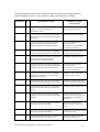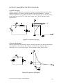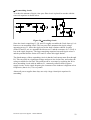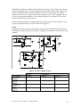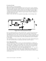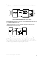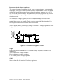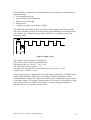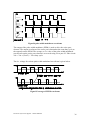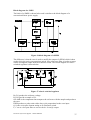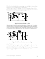
1
Electronics
Power Supplies
(Higher)
5825
September 1999
HIGHER STILL
DET: Electronics
Power Supplies
Higher
Support Materials
CONTENTS
LECTURER'S /TEACHER'S INFORMATION AND SUPPORT MATERIAL
Section 1
The learning outcomes to be covered in the unit
Section 2
Teaching and learning advice including how to use the resource material
Section 3
Details of starting points based on Electronic and Electrical Fundamentals (Int. 2)
Section 4
Assessment procedures showing what is to be assessed, when it is to be assessed and
result recording procedures
Section 5
Resource requirements including course notes, laboratory sheets, book list,
audio/visual aid list
Section 6
Electronics laboratory requirements including technical information sources,
components, materials, facilities and equipment
Section 7
Safety
Section 8
Acknowledgements.
STUDENT'S INFORMATION AND SUPPORT MATERIAL
Section 1
An outline of the outcomes to be covered in the unit
Section 2
The assessment instruments for the outcomes
Section 3
The required achievement standard for each assessment
Section 4
Student's guide to working on the unit
Section 5
Information sheets/references for safety and laboratory work
Section 6
Rectification.
Section 7
Smoothing
Section 8
Voltage regulation
Section 9
Switching mode power supplies.
Section 10
Answers to SAQs
Section 11
Tutorial Questions
Electronics (H): Power Supplies – Teacher/Lecturer Materials
Electronics (H): Power Supplies – Teacher/Lecturer Materials
SECTION 1: LEARNING OUTCOMES
Outcome 1
Identify a rectification circuit and interpret its operation.
Performance criteria
a. A rectification circuit is correctly identified.
b. Circuit voltage levels are accurately measured and recorded.
c. The operation of a rectification circuit is correctly interpreted.
Note on the range of the outcome
Rectification circuit: full-wave; half-wave
Evidence requirements
Written, oral and graphical evidence to show that the candidate can record input and
output voltages, and draw neat, annotated input/output waveforms and from them
correctly identify the operation of the rectifier circuits.
Performance evidence that the candidate can measure input and output voltages, and
correctly identify and interpret the operation of the rectifier circuit.
Outcome 2
Identify power supply filter circuits and interpret their operation.
Performance criteria
a. The filter circuit is correctly identified.
b. Circuit voltage levels are accurately measured and recorded.
c. The operation of a filter circuit is correctly interpreted.
Note on the range of the outcome
Filter circuit: capacitor or capacitor and resistor.
Evidence requirements
Written, oral and graphical evidence to show that the candidate can record input and
output voltages, and draw neat, annotated input/output waveforms.
Performance evidence that the candidate can measure input and output voltages, and
correctly identify and interpret the operation of the filter circuit.
Electronics (H): Power Supplies – Teacher/Lecturer Materials
1
Outcome 3
Identify power supply stabilisation / regulation and protection circuits and interpret
their operation.
Performance criteria
a. Stabilisation / regulation and protection circuits are correctly identified.
b. Load regulation is determined for a pre-constructed circuit.
c. The operation of a stabilisation / regulation circuit is clearly described.
d. The operation of a 3 terminal integrated circuit voltage regulator is clearly
described.
Note on the range of the outcome
Stabilisation / regulation: zener, series pass transistor.
Evidence requirements
Written, oral and graphical evidence to show that the candidate can clearly describe
the action of a protection circuit.
Performance evidence that the candidate can measure and record correctly the output
voltage for a range of loads and identify correctly the regulation and protection
circuits.
Outcome 4
Identify switched mode power supplies and interpret their operation.
Performance criteria
a. The different sections are correctly identified in a switch mode power supply.
b. The operation of a switch mode power supply is clearly explained.
c. The operation of the switch mode power supply is tested / simulated.
Note on the range of the outcome
Sections: rectifier; filter; switch mode controller; switching transistor.
Operation: output regulation; ripple voltage variations; efficiency.
Evidence requirements
Written, oral and graphical evidence to show that the candidate can explain correctly
the operation of a switch mode power supply in terms of power supply, output voltage
and load.
Performance evidence that the candidate can correctly identify the different sections
of a switch mode power supply and can accurately measure the output voltage with
varying levels of load.
Electronics (H): Power Supplies – Teacher/Lecturer Materials
2
SECTION 2 TEACHING AND LEARNING ADVICE INCLUDING HOW TO
USE THE RESOURCE MATERIAL
Teaching Methods
In general the teaching and learning methods used are very dependent on the content
of the unit and the facilities and expertise available at the delivering centre. By their
very nature, however, the units in the Higher Electronics Course suggest the following
teaching methods:
•
Laboratory based learning activities
•
Use demonstration circuits where possible
•
Use student centred circuit testing and analysis
•
Relate essential theory to circuit applications
•
Place components used in a commercial contexts
It is important that all the teachers/lecturers working on the Higher Electronics Course
share a commitment to these methods and employ them as much as possible. In
addition other methods may be identified such as Computer Based Training if the
centre has such a facility. The outcome of this should be a teaching ethos which
pervades the course and sets it apart from other courses which will enjoy a different
background.
POWER SUPPLIES UNIT DELIVERY
MAIN TOPICS
DELIVERY SUGGESTED
OUTCOME 1
Half-wave rectification
Explain the theory and technology, tutorial
examples. Practical exercises.
Full-wave rectification
Explain the theory and technology, tutorial
examples. Practical exercises.
OUTCOME 2
Filter capacitor
Explain the theory and technology, tutorial
examples.
Ripple voltage
Explain theory, practical exercise.
OUTCOME 3
Zener shunt stabiliser, series pass regulator
Explain the theory and technology, tutorial
examples. Practical exercises.
Short-circuit current protection, over voltage protection
circuits
Explain the theory and technology, tutorial
examples.
Electronics (H): Power Supplies – Teacher/Lecturer Materials
3
MAIN TOPICS
DELIVERY SUGGESTED
OUTCOME 3 CONTINUED
Three terminal voltage regulator
Literature searches, data sheets, explain
technology, benefits and use.
Load regulation
Explain theory, practical exercises.
OUTCOME 4
Components of a switch mode power supply (SMPS)
Relate the circuit of the SMPS to the general block
diagram of a power supply. Explain circuit
operation.
SMPS characteristics
Practical exercise to determine regulation, ripple
voltage and efficiency.
Electronics (H): Power Supplies – Teacher/Lecturer Materials
4
SECTION 3: STARTING POINTS
Details of starting points based on Electronic and Electrical Fundamentals
(Int 2)
The units in Electronic and Electrical Fundamentals (Int. 2) have been reviewed for
starting points for the teaching of topics in Power Supplies (H). Relevant outcomes
are identified using the Power Supplies (H) outcomes as the basis.
Power Supplies Learning Outcome 1
Identify a rectification circuit and interpret its operation.
The main topics are half-wave rectification, full-wave rectification, measuring and
recording input/output waveforms.
Starting points from Electrical
Fundamentals (Int 2)
Current and voltage relationships, power
and energy concepts, electromagnetic
fields and their interaction, generation of
an e.m.f., r.m.s. and peak values.
Starting points from
Introduction to
Semiconductor
Applications (Int 2)
Semiconductor diodes, diode characteristics,
forward voltage drop, peak inverse voltage,
measurement of input/output voltages.
Starting points from
Combinational Logic (Int
2)
None.
Electronics (H): Power Supplies – Teacher/Lecturer Materials
5
Power Supplies Learning Outcome 2
Identify power supply filter circuits and interpret their operation.
The main topics are the application of smoothing capacitors, use of low pass RC
filters and ripple voltage.
Starting points from Electrical
Fundamentals (Int 2)
The determination of current and voltage
relationships in d.c. networks.
Starting points from
Introduction to
Semiconductor
Applications (Int 2)
Diode forward voltage drop and
measurement of circuit voltage levels.
Starting points from
Combinational Logic (Int
2)
None
Electronics (H): Power Supplies – Teacher/Lecturer Materials
6
Power Supplies Learning Outcome 3
Identify power supply stabilisation/regulation and protection circuits
and interpret their operation.
The main topics are the interpretation of the block diagram of a power supply, over
voltage crowbar protection, short circuit current protection and integrated circuit
voltage regulators.
Starting points from Electrical
Fundamentals (Int 2)
The determination of current and voltage
relationships in d.c. networks, for
example voltage division and current
division.
Starting points from
Introduction to
Semiconductor
Applications (Int 2)
Zener diode, transistor amplifier,
operational amplifier comparator,
measurement of circuit voltage levels
and operation of SCR.
Starting points from
Combinational Logic (Int
2)
None
Electronics (H): Power Supplies – Teacher/Lecturer Materials
7
Power Supplies Learning Outcome 4
Identify switched mode power supplies and interpret their operation.
The main topics are interpretation of the block diagram, pulse width modulation,
transistor switching, LC filter, flyback diode, switching frequency and duty cycle.
Starting points from Electrical
Fundamentals (Int 2)
The determination of current and voltage
relationships in d.c. networks, for
example voltage division and current
division. Power, current and voltage
relationship.
Starting points from
Introduction to
Semiconductor
Applications (Int 2)
Zener diode, transistor operation,
operational amplifier comparator and
measurement of circuit voltage levels.
Starting points from
Combinational Logic (Int
2)
None
Electronics (H): Power Supplies – Teacher/Lecturer Materials
8
SECTION 4: ASSESSMENT
Assessment procedures showing what is to be assessed, when it is to be assessed
and result recording methods.
Using the instrument of assessment
The Power Supplies unit is assessed using only four instruments of assessment. All of
the Performance Criteria are assessed by laboratory reports. The laboratory
assignments include test questions that ensure all Performance Criteria are assessed.
Electronics (H): Power Supplies – Teacher/Lecturer Materials
9
The following table shows how assessment tasks are related to Learning Outcomes
and Performance Criteria. It also lists the evidence that should be collected.
OUTCOME
PC
1
a)
Learning Outcome 1 laboratory assignment
question on the identification of a
rectification circuit
Graphical / written restricted
response question answers.
b)
Learning Outcome 1 laboratory assignment to
measure and record rectifier input and output
waveforms.
Annotated graphical response.
c)
Learning Outcome 1 laboratory assignment
question to explain the operation of the
rectifier using the waveforms of PC1(b)
Written restricted response
question answers.
All evidence to be contained in
one report for outcome 1.
a)
Learning Outcome 2 laboratory assignment
question on the identification of a filter circuit
Graphical / written restricted
response question answers.
b)
Learning Outcome 2 laboratory assignment to
measure and record filter capacitor
waveforms with and without load.
Annotated graphical response.
c)
Learning Outcome 2 laboratory assignment
question to interpret the operation of the filter
capacitor using the waveforms of PC2(b)
Written restricted response
question answers.
All evidence to be contained in
one report for outcome 2.
a)
Learning Outcome 3 laboratory assignment
questions on identification of stabilisation
and protection circuits
Graphical / written restricted
response question answers.
b)
Learning Outcome 3 laboratory assignment to
investigate load regulation of a given circuit.
Laboratory report for Outcome 3
covering a pre-constructed circuit
c)
Learning Outcome 3 laboratory assignment to
explain the operation of the circuit tested in
PC (b)
Laboratory report for Outcome 3
d)
Learning Outcome 3 laboratory assignment
questions on the operation of a three terminal
regulator
Written restricted response
question answers All evidence to
be contained in one report for
Outcome 3.
a)
Learning Outcome 4 laboratory assignment to
investigate sections of a SMPS
Written restricted response
question answers in laboratory
report
b)
Learning Outcome 4 laboratory assignment to
investigate operation of a SMPS
Written response question answers
in laboratory report
c)
Learning Outcome 4 laboratory assignment to
test the SMPS analysed in PC (a), (b)
Laboratory report to contain all
evidence for Outcome4
2
3
4
ASSESSMENT TASK
Electronics (H): Power Supplies – Teacher/Lecturer Materials
EVIDENCE TO BE
COLLECTED
10
The timing and duration of assessment
This unit progresses the student from the initial stages of linear power supplies to the
full circuits for linear power supplies and switch mode power supplies.
Learning Outcome 1 covers rectification, Learning Outcome 2 deals with smoothing,
Learning Outcome 3 develops linear power supplies and integrated circuit regulators
and Learning Outcome 4 tackles the more complex circuits of switched mode power
supplies. As a consequence the Learning Outcomes should be delivered and assessed
in the order presented in the unit descriptor. The assessments should follow the
conclusion of the teaching for each outcome.
Learning Outcome 1 assessment, laboratory assignment on rectification, should be
delivered after the teaching of this topic. As an integral part of the teaching students
should be given opportunities to attempt questions on rectification similar to those
likely to be encountered in the end of topic laboratory assignment. This will reinforce
teaching while preparing the student for assessment. All students must test either halfwave or full-wave rectification circuits. The laboratory exercise should be allocated
about 120 minutes including the completion of a pro forma report. This should be an
integrated learning and assessment activity with emphasis clearly on learning while
assessment evidence is generated as natural product.
Learning Outcome 2 assessment, laboratory assignment on power supply filters,
should be delivered after the teaching of that topic. As an integral part of the teaching
students should be given opportunities to attempt questions on capacitor smoothing
similar to those likely to be encountered in the end of topic laboratory assignment.
This will reinforce teaching while preparing the student for assessment. All students
must test filter circuits with and without load. The laboratory exercise should be
allocated about 120 minutes including the completion of a pro forma report. This
should be an integrated learning and assessment activity with emphasis clearly on
learning while assessment evidence is generated as a natural product.
For the more able students laboratory assignments for Learning Outcomes 1 and 2
may be cascaded and performed after the delivery of the appropriate teaching
materials.
Learning Outcome 3 assessment, laboratory assignment on load regulation and the
operation of power supply circuits and should be delivered after the teaching of that
topic. As an integral part of the teaching students should be given opportunities to
attempt questions on regulation and circuit operation, similar to those likely to be
encountered in the end of topic test and laboratory assignment. This will reinforce
teaching while preparing the student for assessment. All students must test a
stabilisation/regulation circuit with various loads. The laboratory exercise should be
allocated about 95 minutes including the completion of a pro forma report. This
should be an integrated learning and assessment activity with emphasis clearly on
learning while assessment evidence is generated as a natural product.
Electronics (H): Power Supplies – Teacher/Lecturer Materials
11
Learning Outcome 4 assessment, laboratory assignment on switched mode power
supply, should be delivered after the teaching of that topic. As an integral part of the
teaching students should be given opportunities to attempt questions on switched
mode power supplies similar to those likely to be encountered in the end of topic
laboratory assignment. This will reinforce teaching while preparing the student for
assessment. All students must test/simulate a SPMS with varying load. The laboratory
exercise should be allocated about 60 minutes including the completion of a pro
forma report. This should be an integrated learning and assessment activity with
emphasis clearly on learning while assessment evidence is generated as natural
product.
In principle, there are no time limits for the completion of each instrument of
assessment, but it is likely that a maximum time will be allocated for the completion
of each assignment. It is expected, however, that the average student will complete
the work within the maximum time allowed. The table below indicates the
recommended time allocated for each instrument of assessment.
Learning Outcome
1
2
3
4
Suggested time
120 minutes
120 minutes
95 minutes
60 minutes
It should be noted that the assessment instruments for this unit are all investigative
laboratory assignments. These assignments should be an integral part of the learning
process used to develop the student's knowledge, understanding and experience of the
technology. They should produce assessment evidence that the student has reached a
satisfactory achievement level as a natural product of the teaching and learning
process.
Electronics (H): Power Supplies – Teacher/Lecturer Materials
12
Reassessment
Time is allowed within units for the assessment and reassessment of outcomes.
Where a student has not attained the standard necessary to pass a particular outcome
or outcomes, there should be an opportunity to be reassessed. Reassessment should
focus on the outcome(s) concerned and, as a general rule, should be offered on a
maximum of two occasions following further work on areas of difficulty. Evidence
from the original unit assessment, should assist teachers and lecturers to identify why
an individual student has failed to achieve a particular outcome and to plan focused
support for learning.
For all the outcomes the reassessment should be based on the original instrument of
assessment.
When students have not produced a satisfactory answer to a section of an assessment
they should only be asked to repeat those sections in which they have not provided
suitable responses. Students should be asked to complete the reassessment under the
original controlled conditions. This reassessment should take place as soon as
practical after the initial assessment and after discussion and analysis of the initial
assessment has taken place between the student and the assessor. Students should be
informed of the sections of the assessments that they are required to repeat and given
additional teaching to help them tackle the reassessment. When there is a substantial
number of students requiring reassessment a revision lesson on the problem area
should be presented before reassessment.
Students may produce an answer which is substantially correct but which contains
minor errors such as the mislabelling of a diagram or the incorrectly reading of an
instrument (100 mA instead of 10 mA). In this situation students should be
reassessed by asking them to give the correct answer orally. This should take place as
soon as possible after the initial assessment and before any fuller discussion or
analysis of it.
In the laboratory it is important that the focus is on power supply technology and that
the student's attention is not distracted by other issues such as the use of test
equipment and the recording of results. To this end students attempting this unit
should be familiar with any test equipment or simulation software used and be able to
record and interpret the readings taken from it. The assessor should distinguish
between assessment difficulties resulting from a student's weakness in the use of test
equipment or simulation software and a lack of understanding of power supply
technology. If the student is weak in the use of test equipment or simulation software
this should be resolved by additional training followed by the repeating of the
requisite tests by the student.
Electronics (H): Power Supplies – Teacher/Lecturer Materials
13
The conditions under which assessment takes place
Arrangements documents refer to assessment being carried out under controlled
conditions to ensure reliability and credibility. For the purposes of internal
assessment, this means that assessment evidence should be compiled under
supervision to ensure that it is the student’s own work. Supervision may be carried out
by a teacher, invigilator or other responsible person, for example, a workplace
provider.
The assessments should take place in a laboratory adequately equipped with the
necessary test equipment or simulation software. Ideally students should work
individually but they may be allowed to work in pairs provided individual answer
sheets are prepared. Students should not have access to teaching notes or texts on
power supply technology but should complete the assessments from their own
knowledge and understanding.
It is recommended that the assessments are introduced using the following procedure:
• allow the students a few moments to read the laboratory assignment sheet
• review and summarise the tasks required by the assignment
• identify the equipment and facilities provided for the assignment
• explain the operating conditions within the laboratory
• emphasise safety practices and precautions.
Students should be encouraged to identify themselves to the assessor on completion of
the assignment and before any equipment is dismantled. The assessor should, if
possible, mark the assignment and provide immediate feedback to the student
regarding the outcome. If necessary remedial action should be performed
immediately by the student.
Using internal assessment evidence to contribute to course estimates
The assessments for this unit are designed largely for internal assessment purposes
and have only limited potential to generate evidence for external assessment
performance. Since the assessments are all laboratory assignments they offer limited
opportunities to provide evidence of a students likely performance in an external
exam based assessment. Only the parts of the assignments which require the student
to test and interpret the operation of a circuit offer opportunities to provide evidence
for likely performance in the external assessment.
Electronics (H): Power Supplies – Teacher/Lecturer Materials
14
Advice on the recording and retention of evidence.
Regular meetings and informal discussions between internal verifiers and assessors
facilitate good assessment practice. By using this approach assessors should
understand that internal assessors are matching the internal assessments with external
standards.
Internal verifiers sample records, observe a sample of assessments, countersign
recording documents, support and guide assessors and are involved where disputes
and appeals arise.
All evidence in the form of laboratory results/reports should be retained in case of
appeals or disputes. Below is an example of a checklist, which could also be used to
record results.
Electronics (H): Power Supplies – Teacher/Lecturer Materials
15
Unit Number:
Unit Title: Power Supplies
Date:
OUTCOME 1
Student’s Name
Class
Assessor
TUTOR COMMENTS
satisfactory
unsatisfactory
OUTCOME 2
TUTOR COMMENTS
satisfactory
unsatisfactory
OUTCOME 3
TUTOR COMMENTS
satisfactory
unsatisfactory
OUTCOME 4 PC a)
TUTOR COMMENTS
satisfactory
unsatisfactory
OUTCOME 4
PC b) AND c)
TUTOR COMMENTS
satisfactory
unsatisfactory
Electronics (H): Power Supplies – Teacher/Lecturer Materials
16
Section 5
Resource requirements including course notes, book list, audio/visual aid list.
Course notes
Student notes on Power Supplies are provided in the Student’s Support Material.
These should be either adopted by the centre or modified to suit the teaching approach
taken and the equipment available.
Laboratory sheets
Much of the Performance Criteria of Power Supplies require students to operate test
instruments in conjunction with power supply circuits. Laboratory sheets for each
outcome covering the range statements are available in the NABs pack.
These should be either adopted by the centre or modified to suit the teaching approach
taken and the equipment available. Further circuits may be added to the list provided
the circuits meet with the unit’s performance criteria.
Book list
Electronics for Today and Tomorrow, Tom Duncan, John Murray,
ISBN 0-7195-7413-7
Electronic Devices and Circuits, Bogart, Merrill Publishing Company,
ISBN 0675-21150-6
Applied Electronics, John C Morris, Arnold, ISBN0-340-65284-5
Electronics: Practical Applications and Design, John C Morris, Arnold,
ISBN 0-340-50427-7
Crash Course in Electronics Technology, Louis E Frenzel, Newnes,
ISBN 0-7506-9710-5
ESM Electronics Service Manual, Wimborne Publishing Ltd, Allen House, East
Borough, Wimborne, Dorset BH21 1PF. Tel: 01202 881749, Fax: 01202 641692
Electronics (H): Power Supplies – Teacher/Lecturer Materials
17
Audio/visual aids
The electronics teaching laboratory should have prominently displayed an electrical
safety notice. These are available from a variety of electrical and electronic wholesale
outlets and distributors and are relatively inexpensive.
Component manufacturers and distributors offer wall charts and posters showing
many aspects of electronics. These vary from resistor colour codes to product
processing details and application advertisements. They are generally free and
available on request. They are useful as visual aids on the walls of the electronics
teaching laboratory as they create atmosphere and over a period of time act as a
constant reminder to students.
Data booklets
Technological Studies Data
Booklet
Robert Gibson and Sons, 17 Fitzroy Place,
Glasgow G3 7SF
Electrical Formulae Booklets
These should be either constructed by the
student or provided by the teaching section.
Their main advantage is that they are tailored to
fit the courses on offer.
Electronics (H): Power Supplies – Teacher/Lecturer Materials
18
SECTION 6
Electronics laboratory requirements including technical information sources,
components, materials, facilities and equipment.
Technical information sources
It should be noted that developments in electronics, communications and computing
continue to offer tremendous opportunities for the dissemination and retrieval of
information. At the time of writing the Internet, CD ROM and on-line component
distributors catalogues and web sites for manufacturers, suppliers and providers of
educational material are current examples. All of these and similar potential future
products originate from electronics technology. Accordingly students should be
encouraged to use them and to explore and take advantage of such technological
products as they emerge. A culture of using the technology to its limits should be
encouraged.
There are numerous sources of technical information on electronics other than the
traditional library books. These sources, however, are only helpful if they are both
accessible and relevant. The following has been refined through use and experience
but inevitably will be superseded by better methods as the technology advances and
they become available.
Component Distributors Catalogues
MPS [Maplin]
Web Site
http://www.maplin.co.uk
E-mail
<recipient>@maplin..co.uk
Telephone: Customer services
01702 554002
Telephone: Free technical helpline
01702 556001
Address
Maplin MPS, Freepost SMU 94, P.O. Box 777, Rayleigh, Essex SS6 8LU
RS
Web Site
http://rswww.com
E-mail
http://rswww.com
Telephone
01536 201201
Telephone: Free technical helpline
01536 402888
Address
RS Components Ltd., P O Box 99, Corby, Northants NN17 9RS
Farnell
Web Site
http://www.farnell.co.uk
E-mail
[email protected]
Telephone: Customer services
0113 2636311
Telephone: Free technical helpline
0133 2799123
Address
Farnell Electronic Components, Canal Road, Leeds, LS12 2TU
Electronics (H): Power Supplies – Teacher/Lecturer Materials
19
Access should be provided for students to one or more of the above Component
Distributors Catalogues in either paper, CD ROM or on-line form.
Selected data books, reference books and specialist texts should also be provided from
those offered by the above sources. There are so many good items on offer it is
impossible to recommend a definitive list that is largely a matter of local preference.
Choices should be based on staff expertise, the teaching and learning approaches used
and the available budget. As many of the smaller specialised texts are low cost it
should be possible to provide several reference copies for use in the electronics
laboratory.
Many manufacturers of electronic components have web sites. These may be located
by a net search using the manufacturer's name. Once into the web site it is often
possible to locate technical data, application information and in some situations,
design tutorials.
Components
The Electronics Laboratory should offer access to component stocks as a standard
facility. This is for the benefit of both staff and students who will require access to
components for demonstrations, experimentation and for case study and project work.
The stock, however, has to be managed and controlled if the quality of the facility is
to be sustained. The approach taken to this is a matter for the centre's organisational
structure but experience suggests that one person needs to be clearly identified as
having responsibility for the stock, for issuing it and for reordering.
Below is a typical basic selection of components.
resistors
Low cost metal film 0.25 W - standard preferred values from 1 Ω to
10 M Ω .
High powered resistors 2.5 W silicon coated- standard available
values.
potentiometers
150 mW carbon trimmers- standard preferred values from 100 Ω to
10 M Ω .
Capacitors
Metallised ceramic plate capacitors-standard preferred values from
1.8 pF to 120 pF
Resin dipped plate ceramic capacitors -standard preferred values
from 10 pF to 0.47 µF
Radial polystyrene capacitors-standard preferred values from 100
pF to 8200 pF
Radial lead electrolytic capacitors-standard preferred values from
1 µF to 47000 µF
Axial lead electrolytic capacitors-standard preferred values from
1 µF to 47000 µF
Electronics (H): Power Supplies – Teacher/Lecturer Materials
20
diodes
1N4148, 1N4001,1N5401,BZX85- range of voltages from 2.7 V to
15 V
bridge rectifier
W005G
light emitting diodes
3 mm and 5 mm red, orange and green
transistors
BC184L, BC214L, 2N3053, BFY50, TIP31A, TIP32A,TIP33A,
2N3055E, 2N2955, 2N3819, 2N3820
op. amps.
µA 741, LM 324N, CA3140E
logic chips
74 LS series TTL - selected functions as appropriate
4000 series CMOS - selected functions as appropriate
other analogue integrated
circuits
NE555N timer, ICM7555 timer, L7805CP, L7812 CP positive
voltage regulators, L7905CT, L7812 CT negative voltage
regulators
other digital integrated circuits
DACs and ADCs to suit laboratory applications
fuses
As required for instruments
switches
Push button, toggle, slide and DIL miniature as required
transformers
As required
lamps and bulbs
Low voltage and power selection to meet requirements
relays
Low voltage as required
connectors
Terminal blocks, 4 mm plugs and sockets in red, black, blue, yellow
and green
Materials
Few materials are required. It may be helpful to have reels of solid and stranded
conductor wire in a variety of colours available. Some are suggested below.
WIRE TYPE
COLOUR
Solid Core Wire (1/0.6)
Black, Blue, Brown, Green, Red, White, Violet,
Yellow
Hook-Up Wire (7/0.2)
Black, Blue, Brown, Green, Red, White, Violet,
Yellow
Electronics (H): Power Supplies – Teacher/Lecturer Materials
21
Facilities
The ideal electronics teaching laboratory has office style or computer tables (wide)
around the walls with matching narrow tables in the middle. A typical plan is shown
below. This type of layout has found favour in a number of centres and so has
clearly proved its worth for several teams of teaching engineers.
Stora ge
a nd
c om pute r
W hite boa rd
Stora ge
a nd
c om pute r
Trunking with 13 Amp socket outlets should be fitted around the walls at a convenient
height above the wide tables. Each student should have available a 2 metre run of
surface and at least four 13Amp socket outlets. This is necessary to allow adequate
working surface for test equipment, circuits, components and papers. Eye level
shelving around the walls above the power socket trunking can also be useful for test
instruments and general storage.
The socket outlets should be protected by a suitable device such as an earth leakage
circuit breaker and a central safety switch with key lock. The design and installation
of such facilities should be undertaken by a specialist as they constitute important
safety features.
The central tables are used for written work and group teaching. Suitable strong
moveable chairs such as those found in hotel conference rooms should be provided in
adequate numbers to allow seating around the wall tables or in the centre but not both.
Excessive furniture and narrow spaces between tables in the laboratory can be a safety
hazard and should be avoided.
Electronics (H): Power Supplies – Teacher/Lecturer Materials
22
Equipment
In the electronics laboratory each student should have access to the following
equipment. Ideally there should be one set of equipment per student.
1.
2.
3.
4.
5.
6.
Multimeter
Dual rail power supply
Signal generator
Double beam oscilloscope
Logic probe
Computer
It is also helpful to have a limited range of tools available such as:
• Snipe nosed pliers
• Wire cutters
• Wire strippers
• Screw drivers
The types of tools and equipment on the market are constantly changing through a
process of continuous improvement. It is strongly recommended that before
purchasing any items for an electronics laboratory advice is sought from a current
user experienced in this area. Issues such as the cost of hand tools in relation to their
quality and life expectancy with inexperienced users who may damage or remove
them from the laboratory have to be given due consideration. Equipment may be
found which is both adequate for the teaching laboratory, student proof and
inexpensive requiring little maintenance.
There are many suppliers of test equipment and tools but only those specialising in the
educational market are likely to offer products at an acceptable price. Similarly these
suppliers are more likely to have tools and equipment which can survive the rigours of
the teaching laboratory. It is good practice to both commercially and technically
survey the market to insure that the best suppliers are offered sales opportunities.
Other centres which have tried and tested equipment are often the best source of
information and should be consulted as part of the purchasing exercise. Suppliers
may provide access to users of their products who are prepared to discuss their
experiences with others. Time spent on this will pay substantial dividends in future
years in terms of equipment downtime and repair costs.
Electronics (H): Power Supplies – Teacher/Lecturer Materials
23
Software
The electronics teaching laboratory is greatly enriched by the presence of PCs with
appropriate software. Since computers are one of the main products of electronics
technology they find extensive use in the application of the technology and form part
of the electronics environment. While the capital outlay for this may be significant
there has to be recognition of the part played by the computer with specialised
software in the electronics environment.
Through access to suitable computing facilities and software students should be
exposed to this environment in the teaching laboratory. Commercial software for
word and data processing is widely available at reasonable cost and is generally
selected by centres to conform with their local policy. These may find application in
the creation of reports and the analysis of results.
In addition, however, circuit simulation and drawing software may also be used but is
less widely available and more difficult to locate in a form which is cost effective for
the teaching laboratory. To meet these criteria the software must be easy to use
without extensive training and be available at low cost with multiple copies site
licensed. While there are several products on the market those which have stood the
test of time and so are favoured for use in colleges and schools are listed below.
Invent ! CROCODILE CLIPS:
simple simulation of electronics and mechanics
Web address
WWW.crocodile-clips.com/education/v3.htm
E-mail
[email protected]
Telephone
0131 226 1511
Fax
0131 226 1522
Address
Crocodile Clips
11 Randolph Place
Edinburgh
EH3 7TA
Electronics Workbench: circuit simulation and testing
Web address
http://www.adeptscience.co.uk
E-mail
info@ adeptscience.co.uk
Telephone
01462 480055
Fax
01462 480213
Address
Adept Science plc
6 Business Centre West
Avenue One
Letchworth
Herts.
SG6 2HB
Electronics (H): Power Supplies – Teacher/Lecturer Materials
24
SmartDraw: drawing of diagrams and plans with associated symbol libraries
Web address
http://www.smart draw.com
E-mail
[email protected]
Telephone
01889 564601
Fax
01889 563219
Address
The Thompson Partnership
Lion Buildings,
Market Place,
Uttoxeter,
Staffs.
ST14 8HZ
Electronics (H): Power Supplies – Teacher/Lecturer Materials
25
SECTION 7: SAFETY
The safety of teaching staff and students working in the electronics laboratory must be
the primary concern of everyone involved.
This has to take precedence over all other activities and be sustained against all
other pressures.
There are many aspects to safety as follows:
• Statutory requirements
• Centre procedures
• Centre structure
• Staff training and behaviour
• Laboratory features
• Student training and behaviour.
It is beyond the scope of this document to provide details of all of these items which
should be embraced as part of an centre's safety policy. Lecturer's /Teacher's must,
however, be content that all appropriate safety measures are in place before
embarking on work within the electronics laboratory.
Student training is a recurrent activity which is likely to be the direct responsibility of
the lecturer/teacher. While this has to take place on a continuous basis as work in the
laboratory proceeds it is helpful to perform specific safety training at course
commencement. Such training might form part of the course induction as its
relevance extends across all course units. This is particularly important for
electronics students as they should be encouraged to develop their own safety culture
which should become a lifelong asset.
Lecturers/teachers performing safety training for students may find a rich diversity of
available material. Of specific relevance, however, is a teaching package prepared by
the University of Southampton's Department of Electrical Engineering and Teaching
Support and Media Services. The package was prepared in association with and
financially supported by the Health and Safety Executive. It consists of :
• Handbook: 'Safety Handbook for Undergraduate Electrical Teaching Laboratories'
• Video Programme: 'Not to Lay Blame'
• A booklet: 'Tutor's Guide'
The package is targeted at the first year undergraduate level and works well with other
students at similar levels. The handbook is very comprehensive and sufficiently
inexpensive to be bought in quantity and given to students for everyday use. It is well
presented using text and cartoons. The video dramatises issues associated with
electrical/electronics laboratory work using a style and characters likely to appeal to
the majority of students. The Tutor's Guide booklet rounds the package off by giving
guidance on the use of the video and handbook. In addition it contains 'Safety Rules
for Electrical Laboratories' and a comprehensive list of references to enable further
reading should you wish it.
Electronics (H): Power Supplies – Teacher/Lecturer Materials
26
At the time of writing the distribution of the package was the subject of discussions.
To find out the current situation contact:
Maggie Bond
Department of Electrical Engineering
University of Southampton
SO17 1BJ
Phone 01703 595164
Email [email protected]
Electronics (H): Power Supplies – Teacher/Lecturer Materials
27
SECTION 8: ACKNOWLEDGEMENTS
We gratefully acknowledge the support and assistance provided by colleagues at Stow
College who have contributed material and helpful advice for this pack.
We would also acknowledge with thanks lecturers and teachers in other colleges and
schools who have assisted in the preparation of the pack by contributing material and
by commenting on draft documents.
Electronics (H): Power Supplies – Teacher/Lecturer Materials
28
STUDENT’S INFORMATION
AND SUPPORT MATERIAL
Electronics (H): Power Supplies – Student Materials
1
Electronics (H): Power Supplies – Student Materials
2
SECTION 1: LEARNING OUTCOMES
Outcome 1
Identify a rectification circuit and interpret its operation.
Performance criteria
a. A rectification circuit is correctly identified.
b. Circuit voltage levels are accurately measured and recorded.
c. The operation of a rectification circuit is correctly interpreted.
Note on the range of the outcome
Rectification circuit: full-wave; half-wave
Evidence requirements
Written, oral and graphical evidence to show that the candidate can record input and
output voltages, and draw neat, annotated input/output waveforms and from them
correctly identify the operation of the rectifier circuits.
Performance evidence that the candidate can measure input and output voltages, and
correctly identify and interpret the operation of the rectifier circuit.
Outcome 2
Identify power supply filter circuits and interpret their operation.
Performance criteria
a. The filter circuit is correctly identified.
b. Circuit voltage levels are accurately measured and recorded.
c. The operation of a filter circuit is correctly interpreted.
Note on the range of the outcome
Filter circuit: capacitor or capacitor and resistor.
Evidence requirements
Written, oral and graphical evidence to show that the candidate can record input and
output voltages, and draw neat, annotated input/output waveforms.
Performance evidence that the candidate can measure input and output voltages, and
correctly identify and interpret the operation of the filter circuit.
Electronics (H): Power Supplies – Student Materials
3
Outcome 3
Identify power supply stabilisation / regulation and protection circuits and interpret
their operation.
Performance criteria
a. Stabilisation / regulation and protection circuits are correctly identified.
b. Load regulation is determined for a pre-constructed circuit
c. .The operation of a stabilisation / regulation circuit is clearly described
d. .The operation of a 3 terminal integrated circuit voltage regulator is clearly
described.
Note on the range of the outcome
Stabilisation / regulation: zener, series pass transistor.
Evidence requirements
Written, oral and graphical evidence to show that the candidate can clearly describe
the action of a protection circuit.
Performance evidence that the candidate can measure and record correctly the output
voltage for a range of loads and identify correctly the regulation and protection
circuits.
Outcome 4
Identify switched mode power supplies and interpret their operation.
Performance criteria
a. The different sections are correctly identified in a switch mode power supply.
b. The operation of a switch mode power supply is clearly explained.
c. The operation of the switch mode power supply is tested / simulated.
Note on the range of the outcome
Sections: rectifier; filter; switch mode controller; switching transistor.
Operation: output regulation; ripple voltage variations; efficiency.
Evidence requirements
Written, oral and graphical evidence to show that the candidate can explain correctly
the operation of a switch mode power supply in terms of power supply, output voltage
and load.
Performance evidence that the candidate can correctly identify the different sections
of a switch mode power supply and can accurately measure the output voltage with
varying levels of load.
Electronics (H): Power Supplies – Student Materials
4
SECTION 2: ASSESSMENT INSTRUMENTS
The assessment instruments for the outcomes
The Power Supplies unit covers the different sections comprising a power supply.
Each outcome addresses a particular section, therefore you will be involved with
assessment activities for all the four outcomes.
Learning Outcome 1 deals with half-wave and full-wave rectification circuits .You
will be asked to identify and test various rectification circuits and measure and record
input/output waveforms. You will then be required to explain the operation of the
circuit under investigation using the data acquired during testing.
If necessary you should seek clarification from your lecturer/teacher before you start
any laboratory exercise, review your progress as you proceed and submit your pro
forma report for comment on completion. You may prefer to work on this with a
friend but you should both contribute equally as team members and submit individual
reports at the end. You are unlikely to be allowed to work in teams of more than two,
as there is not enough in the tests to occupy you fully.
The laboratory exercise for Learning Outcome 1 should take about 90 minutes to
complete (certainly not any more than 120 minutes).
Learning Outcome 2 covers smoothing/filtering circuits. You will be asked to identify
and test various smoothing/filter circuits, measure and record input/output waveforms.
You will then be required to explain the operation of the circuit under investigation
using the data acquired during testing.
If necessary you should seek clarification from your lecturer/teacher before you start
the laboratory exercise, review your progress as you proceed and submit your pro
forma report for comment on completion. You may prefer to work on this with a
friend but you should both contribute equally as team members and submit individual
reports at the end. You are unlikely to be allowed to work in teams of more than two,
as there is not enough in the tests to occupy you fully.
The laboratory exercise for Learning Outcome 2 should take about 90 minutes to
complete (certainly not any more than 120 minutes).
If you are well prepared and work efficiently then you may be able to perform the
laboratory exercises for Learning Outcome 1 and 2 in one laboratory time slot.
Consult your course lecturer/teacher.
Learning Outcome 3 examines linear integrated circuit voltage regulators, basic
power supply regulation/stabilisation circuits as well as over voltage and short circuit
protection circuits. The assessment instrument is a laboratory assignment in which
you will be required to test a pre-constructed linear voltage stabilisation/regulation
circuit. This involves measuring the output voltage for varying levels of load and
using this information to explain the operation of the circuit under investigation.
This laboratory assignment will also test your knowledge of over voltage protection,
short circuit protection and the operation of integrated voltage regulators.
Electronics (H): Power Supplies – Student Materials
5
If necessary you should seek clarification from your lecturer/teacher before you start
the laboratory exercise, review your progress as you proceed and submit your pro
forma report for comment on completion. You may prefer to work on this with a
friend but you should both contribute equally as team members and submit individual
reports at the end. You are unlikely to be allowed to work in teams of more than two,
as there is not enough in the tests to occupy you fully.
The laboratory exercise for Learning Outcome 3 should take about 95 minutes to
complete
Learning Outcome 4 concentrates on switched mode power supplies (SMPS) .The
assessment instrument is a laboratory assignment in which you will be asked to
identify the different section of a SMPS, test/simulate a SMPS and use the
experimental data to explain the operation of the SMPS.
If necessary you should seek clarification from your lecturer/teacher before you start
the laboratory exercise, review your progress as you proceed and submit your pro
forma report for comment on completion. You may prefer to work on this with a
friend but you should both contribute equally as team members and submit individual
reports at the end. You are unlikely to be allowed to work in teams of more than two,
as there is not enough in the tests to occupy you fully.
The laboratory exercise for Learning Outcome 4 should take about 60 minutes to
complete
Electronics (H): Power Supplies – Student Materials
6
SECTION 3: ASSESSMENT STANDARDS
The required achievement standard for each assessment
Learning Outcome 1 Rectification Assessment
The laboratory report test questions and the practical activities are designed to match
the Performance Criteria for the Learning Outcome. Because of this you will have to
reach a minimum standard in both the test questions and the practical activities to gain
a pass.
Learning Outcome 2 Power Supplies Filter Circuit Assessment
The laboratory report test questions and the practical activities are designed to match
the Performance Criteria for the Learning Outcome. Because of this you will have to
reach a minimum standard in both the test questions and the practical activities to gain
a pass.
Learning Outcome 3 Linear Power Supplies Assessment
The laboratory report test questions and the practical activities are designed to match
the Performance Criteria for the Learning Outcome. Because of this you will have to
reach a minimum standard in both the test questions and the practical activities to gain
a pass.
Learning Outcome 4 Switched Mode Power Supplies Assessment
The laboratory report test questions and the practical activities are designed to match
the Performance Criteria for the Learning Outcome. Because of this you will have to
reach a minimum standard in both the test questions and the practical activities to gain
a pass.
NOTE:
For each of the circuits you are testing you are expected to understand and explain its
operation. This may involve performing calculations, drawing and interpreting graphs
or waveforms and suggesting uses for the circuit. Your reports should have adequate
information in them to convince your tutor that have correctly tested the circuit and
that you understand its operation. You are required to complete this for four circuits:
• Full-wave rectifier circuit
• Filter circuit
• Power supply stabilisation circuit
• SMPS circuit
Electronics (H): Power Supplies – Student Materials
7
SECTION 4: STUDENT GUIDE
Power supplies are used in most electronic equipment, for example, computers,
amplifiers, alarm systems and televisions. Consequently it is important that electronic
technician engineers have a good grasp of the fundamentals of stabilised power
supplies.
Learning Outcome 1 explores rectification, that is, converting a.c. waveforms into d.c.
waveforms. In this outcome you are required to measure and record a.c. and d.c.
waveforms. To prepare yourself for this outcome and the practical aspects of the
remaining outcomes you should familiarise yourself with:
• test instruments, such as the oscilloscope, the signal generator, and the multimeter
• tools such as wire strippers, wire cutters, soldering iron, bread-board
• electronic circuit simulation software.
To improve your knowledge and understanding of the subject material you should
simulate given circuits and take heed of instrument readings in the simulation
software.
Learning Outcome 2 investigates power supply filtering and again your are required
to measure and to record waveforms. The type of filtering normally used is capacitive,
however your background reading for this outcome should include capacitor charging
and discharging, CR and RC networks and low pass LC filter circuits.
To improve your knowledge and understanding of the subject material you should
simulate given circuits and take heed of instrument readings in the simulation
software.
Learning Outcome 3 looks at the sub circuits and then at the complete circuits that
make a stabilised power supply. These circuits are composed of active devices such as
transistors, zener diodes, operational amplifiers and thyristors. It would be to your
advantage to revise the operation of these devices. To improve your knowledge and
understanding of the subject material you should simulate given circuits and take note
of instrument readings in the simulation software.
Learning Outcome 4 introduces switched mode power supplies. To prepare for this
outcome you should study how the transistor works as a switch, investigate how a
pulse width modulated waveform is produced, identify the purpose of a flyback diode,
understand the properties of an inductor and examine manufacturer’s data on SMPS
integrated circuits.
To improve your understanding of power supplies you should source the power
supply circuits in a computer or amplifier and try to identify the various sections
being studied on the course and try to describe the operation of the circuits. It is also
useful to investigate power supply specifications, these give a measure of the quality
of the regulation circuit. You can also obtain valuable information over the Internet
and by browsing through manufacturer’s catalogues. Since this unit is laboratory
based and may involve you in the use of transformers directly fed from the mains, you
must pay due attention to all safety procedures set down for the practical activities of
this unit.
Electronics (H): Power Supplies – Student Materials
8
SECTION 5: INFORMATION SHEETS/REFERENCES FOR SAFETY AND
LABORATORY WORK
Safety Guidelines for Electronics Laboratory Work.
You should read these guidelines and discuss them with your tutor to clarify their
significance in your working environment
• Enter the Electronics Laboratory only at agreed times
• Enter the Electronics Laboratory only when you are authorised
• You should only work on equipment when a supervisor is present
• Always avoid bulky, loose or trailing clothes, long loose hair, heavy metal
bracelets or watch straps
• Do not take food or drink into the Electronics Laboratory
• Avoid wet hands or clothes and clean up any liquid spillages
• Be as careful for the safety of others as yourself
• Think before you act, be tidy and systematic
• Keep passages and work areas free of obstructions
• Voltages above 120 V d.c. and 50 V rms are always dangerous, take extra
precautions as voltages increase
• Never remove earth connections and make sure that all accessible conducting
parts of equipment or experiments are earthed. If in doubt check for earth
continuity
• Multimeters and hand-held probes should be of good fused design and are not
recommended for dangerous levels of voltage or power
• Understand the correct handling procedures for batteries, capacitors, inductors and
other energy-storage devices. Always handle them carefully
• Fluorescent lights can cause rotating equipment to appear stationary. You should
be aware of this and take precautions if necessary
• Before equipment is made live all casings, covers or shrouds must be in place so
that no live parts can be touched with fingers
• Before equipment is made live all casings, covers or shrouds must be in place so
that no moving parts can be touched with fingers
• Before equipment is made live circuit connections and layouts should be checked
by your supervisor
• If you are working in a group everyone in the group should give there assent
before equipment is made live
• Never make changes to either circuits or mechanical layouts without isolating the
circuit by switching it off and removing connections to supplies
• Experimental equipment left unattended should be isolated from the supply unless
it has to be left on for some special reason, in which case a barrier and warning
notice are required
• Equipment found to be faulty in any way should be reported to your supervisor
immediately and not used until it is inspected and declared safe
• You should know what to do if there is an emergency in the Electronics
Laboratory
• Use hand tools carefully and treat them with respect as they can be dangerous
when misused or faulty
• Do not remove equipment, tools or materials from the Electronics Laboratory
without authorisation from your supervisor
Electronics (H): Power Supplies – Student Materials
9
SECTION 6: STUDENT NOTES ON POWER SUPPLIES
Introduction
Stabilised electronic power supplies are circuits that give out a constant d.c. voltage
irrespective of the current drawn from them and irrespective of the input voltage
changes, provided they are operated within their stated specifications. A battery can
be regarded as a source of constant voltage, that is, different levels of current may be
drawn from it and the voltage across it will remains almost constant. The battery is
very useful for portable equipment unfortunately it has a limited life span, has to be
replaced regularly and therefore electronic power supplies are the preferred option.
Figure 1 compares ideal, practical and unacceptable voltage sources. An ideal voltage
source gives a constant voltage out inspite of the current drawn. A practical voltage
source loses some voltage across its internal resistance hence the output tends to drop
as more and more current is drawn. A poor voltage source begins to drop its output
voltage as soon as current is drawn.
Figure 1 comparison of ideal, practical and poor voltage sources
Most electronic equipment uses stabilised power supplies for reliable operation at
reasonable cost without the need for renewal of the power source. The block diagram
of a stabilised power supply is shown below, in Figure 2.The individual sections of
the block diagram will be developed further in this unit.
Figure 2 power supply block diagram
Electronics (H): Power Supplies – Student Materials
10
Rectification
Normally the d.c. voltages used in electronic systems are much lower than the 230V
a.c. from the mains supply. Therefore prior to rectification the mains voltage is
stepped down using a transformer as illustrated in figure 3.
Figure 3 transformer stepping down the mains voltage
Transformer turns ratio is given by
V1/V2 = N1/N2 = I2/I1
The secondary transformer voltage can be found as follows. If N1: N2 =38:1 then
V2 may be found using the above equation V1/V2 = N1/N2
V2 = (N2/N1 )V1 = (1/38)230 V
=6V
The voltages used in the equations are root mean square (r.m.s.) values and the
frequency of the mains voltage is 50Hz. The peak (pk) of the voltage can be found
from the relationship
Vr.m.s. = Vpk/√2 = 0.707 Vpk
Therefore the maximum transformer output voltage value is equal to √2 x 6 V = 8.5
V, this is shown below in Figure 4.
Electronics (H): Power Supplies – Student Materials
11
Figure 4 sinusoidal waveform
Once the mains voltage has been stepped down it can be rectified .Rectification is the
process of converting a.c. voltages into d.c. voltages.
Half-wave rectification
The electronic device used for rectification is called a diode. Normally a silicon
rectifier diode is capable of passing a few amperes at a forward voltage drop of about
0.6V.It has a high value of peak inverse voltage (PIV), which is sometimes referred to
as maximum reverse voltage (Vrrm).
The basic operation of the diode is shown below in Figure 5.
Electronics (H): Power Supplies – Student Materials
12
Figure 5 (a) forward bias diode, conducts current (b) reverse bias diode, blocks
current flow
When the anode of the diode is about 0.6V more positive than the cathode the diode
conducts and can be regarded as a closed switch. However when the anode voltage is
less than the cathode voltage the diode can be regarded as an open switch as no
current flows through it.
SAQ1
How will the diode behave if the anode voltage is made 2V greater than the cathode
voltage?
Electronics (H): Power Supplies – Student Materials
13
Operation of half-wave rectifiers
Figure 6 half-wave rectifier circuit
The half-wave rectifier is shown in figure 6. When the anode of the diode D1 is
positive, it conducts and current flows from A through D1 and RL to B. This causes a
voltage, with magnitude proportional to the diode current, to be developed across the
load RL. On the negative half-cycle of the input voltage to the rectifier the diode acts
as an open switch and no current flows through it and no voltage is produced across
RL, as shown below in figure 7.
Figure 7 half-wave rectifier input/output waveforms
The output voltage of the half-wave rectifier is called pulsating d.c. or raw d.c., in
other words d.c. does not mean just a horizontal straight line time graph (constant
voltage), but any voltage or current that does not change polarity.
Note that to draw accurate waveforms we need to take into consideration the fact that
the diode does not conduct significantly until the input voltage to the rectifier is just
greater than 0.6V and that when the diode is conducting the voltage drop across it is
0.6V.
Electronics (H): Power Supplies – Student Materials
14
Full-wave rectification using bridge rectifier
Figure 8 full-wave bridge rectifier
When A is positive with respect to B diodes D1 and D3 are forward biased and
current flows as shown by the arrows. The current flow through RL is from the top to
the bottom. During the next half-cycle B is positive with respect to A and the circuit
current flow is as shown in Figure 9, however the current flow through the load RL is
in the same direction. This means that the voltage developed across RL is in the same
direction irrespective of voltage polarities at A and B. Figure 10 shows the rectifier
input and output waveforms.
Figure 9 full-wave bridge rectifier on negative half-cycle
Electronics (H): Power Supplies – Student Materials
15
Figure 10 full-wave bridge rectifier input/output waveforms
Full-wave rectifier using centre-tapped transformer
Figure 11 full-wave rectifier using centre-tapped transformer
When A is positive with respect to C. C is positive with respect to B. Then current
flow is from A through D1and RL then into C. When B is positive with respect to C.
C is positive with respect to A. The current flow is now from B through D2 and RL
then into C. In both these cases the direction of the current through RL is always the
same, hence a d.c. voltage is developed across the load.
Electronics (H): Power Supplies – Student Materials
16
Figure 12 waveforms for full-wave rectifier using centre-tapped transformer
SAQ2
Explain the operation of a full-wave rectifier based on the centre-tapped transformer
using the input/output waveforms
Electronics (H): Power Supplies – Student Materials
17
SECTION 7: SMOOTHING (FILTER CAPACITOR)
Capacitor charging
When a voltage is applied to a capacitor, it charges exponentially to the value of the
applied voltage over a time dependent on the circuit time constant (τ). The time
constant is defined as the product of R and C in the circuit. In fact τ is the time taken
by the capacitor to reach 0.67 of the final voltage value. This is illustrated in the
figure below:
Τ
Figure13a capacitor charging
Capacitor discharging
When a load resistor is connected across a charged capacitor, the capacitor discharges
exponentially to zero volts. In this situation τ is the time the capacitor takes to
discharge to 0.33 of its initial voltage. This is illustrated in the figure below:
Τ
Figure13b capacitor discharging
Electronics (H): Power Supplies – Student Materials
18
Low-pass filter
The low-pass filter (shown below) allows signals at low frequencies to pass through
but attenuates signals at and above the cut-off frequency. For example a low-pass
filter with a cut-off frequency of 100Hz will only allow signals at frequencies below
100Hz to pass with a little change, all other signals will be decreased in size.
Figure14 low-pass filter and its characteristics
Smoothing Capacitor
When a large electrolytic capacitor is connected across a rectifier, it charges quickly
to the peak value of the rectified voltage due to the low forward resistance of the
diode. This electrolytic capacitor is known as a smoothing capacitor or filter capacitor
or reservoir capacitor. The purpose of the capacitor is to convert the pulsating output
of the rectifier into a steady d.c. voltage. However when a load is connected to the
capacitor, the capacitor voltage falls from the peak rectifier voltage, as illustrated
below.
Figure15 half-wave rectifier with capacitor filter and load.
Electronics (H): Power Supplies – Student Materials
19
Figure 16 input/output waveforms for half-wave rectifier with smoothing and
load
Assume that the capacitor has charged to the peak value of the rectified output
voltage. The rectifier output voltage now drops below the capacitor voltage making
the rectifier diode reverse biased. During this time the load current is supplied by the
capacitor and naturally the capacitor voltage drops, as it discharges into RL. The
capacitor voltage continues to fall until the rectifier output voltage exceeds the
capacitor voltage. When this occurs the capacitor charges to the peak rectifier output
voltage and the rectifier supplies the capacitor charging and load currents. This cycle
continues to repeat itself.
Ripple voltage
The voltage across the capacitor is no longer a constant d.c. level but a d.c. level
superimposed on a varying d.c. voltage. This varying waveform is called a ripple
voltage (Vr).The frequency of the ripple voltage is the same as the frequency of
rectifier output wave form. The pk-to-pk value of the ripple voltage depends on the
load . No load gives no ripple, as the load increases so does the magnitude of the
ripple voltage. The effect of load variation on ripple voltage is shown in figure 17.
Electronics (H): Power Supplies – Student Materials
20
Figure 17 Ripple voltage with different loads (time constants)
FULL-WAVE BRIDGE RECTIFIER WITH SMOOTHING
Figure18 full-wave rectifier with smoothing and load
In this circuit the capacitor is charged on both half-cycles and hence the discharge
time for the capacitor is greatly reduced. The overall effect is that given the same time
constant the ripple voltage is reduced for full-wave rectification compared with that
for half-wave rectification. The waveforms for full-wave rectification and smoothing
are given in figure 19, note the ripple frequency is now doubled to 100Hz. The last
waveform is the ripple waveform enlarged.
Electronics (H): Power Supplies – Student Materials
21
Figure 19 ripple waveform for full-wave rectifier
The d.c. (average) value of the rectified smoothed voltage waveform with ripple can
be estimated to be
Vd.c. = Vpk – 0.5Vr
= Vpk – 0.5 x (Vpk / f x R x C)
where
Vd.c.
Vpk
C
R
f
is the d.c value of the smoothed waveform
is the peak rectified output voltage in volts
is the value of the reservoir capacitor in Farads
is the load resistance in ohms
is the frequency of the ripple voltage in volts
Electronics (H): Power Supplies – Student Materials
22
π (pi) smoothing circuit
To reduce the amount of ripple a low-pass filter circuit is placed in cascade with the
reservoir capacitor as shown below.
Figure 20 π smoothing circuit
Since the circuit comprising C1, R1 and C2 roughly resembles the Greek letter pi, it is
known as a π smoothing circuit. The low-pass filter attenuates the ripple voltage
appearing across C1, hence the ripple across the load is further reduced. In other
words R1 and C2 act, as a potential divider across C1and the reactance of C2 (Xc2) is
low at the ripple frequency. The large smoothing capacitor has small ripple across it
and the potential divider action of R1 and C2 reduce this ripple further.
The disadvantage of the π smoothing circuit is that the load current must flow through
R1. This can result in a significant voltage and power loss in the filter, and reduce the
voltage available for the load. This problem can be overcome by replacing the R1 in
the π smoothing circuit with an inductor L1, commonly called a choke in power
supply circuits. At the ripple frequency the reactance of the inductor is high but at low
frequencies (that is d.c.) it is very small.
Almost all power supplies these days use only a large electrolytic capacitor for
smoothing.
Electronics (H): Power Supplies – Student Materials
23
SECTION 8: VOLTAGE REGULATION
The purpose of a d.c. power supply is to provide a constant d.c. output voltage
irrespective of changes in a.c. input voltage or changes in d.c. load current. Most
electronics circuits require this type of supply, that is an extremely constant d.c.
voltage , for guaranteed and reliable operation.
The smoothing circuit is inappropriate for most applications, as a ripple voltage
appears when a load current is drawn. For this reason, in a power supply, a voltage
regulation/stabilisation circuit follows the smoothing capacitor.
To indicate the performance of a power supply two figures are normally used. The
first one is called load regulation and it measures how well the power supply is able to
maintain constant voltage between no-load and full-load conditions. Expressed as a
percentage this is
% load regulation = ((VNL –VFL)/VFL) x 100%
where:
VNL is the no-load output voltage in volts
VFL is the full-load output voltage in volts
SAQ3
The open-circuit voltage of a d.c. power supply is 12V, When a load is applied the
voltage falls to 11.5V. Calculate the % load regulation.
SAQ4
A computer power supply was tested to determine its load regulation. The no load and
full-load measurements were 5V and 4.95V respectively. Calculate the % load
regulation.
SAQ5
Two power supplies have the same no-load voltage. However one has a load
regulation of 10% and the other 5%. Explain which is the better power supply.
The second performance figure for a power supply is line regulation. This indicates
how sensitive the output is to changes in input voltage . Expressed as a % this is
% line regulation = (change in d.c. output voltage/change in a.c. input voltage) x
100%
SAQ6
Calculate the % line regulation if the d.c. output voltage of a power supply changes
from 12V to 11.5v for a change in a.c. line voltage from 220V to 209V
Electronics (H): Power Supplies – Student Materials
24
Stabilisation/Regulation circuits
Zener diode stabiliser
The characteristics of a Zener diode is given in figure 21
Figure21 Zener diode characteristic
The characteristics show that when the diode is forward biased it behaves as a normal
silicon diode. When it is reverse biased the diode breaks down at a predetermined
voltage (Zener voltage) due to the avalanche effect. Once the reverse bias is removed
the diode recovers. Close examination of the reverse bias characteristic also shows
that the voltage across the diode is fairly constant for varying currents through it
(Izmax to Izmin). This property of the Zener diode is utilised in the Zener diode
stabiliser circuit shown below
Figure 22 basic Zener diode shunt stabiliser
The Zener diode is reverse biased and operated in its break down region (at the Zener
voltage). In this state the voltage across the Zener diode remains constant for changes
in current through it. Since the Zener diode is across the load, it sets the output
voltage value. This circuit is referred to as a basic shunt stabiliser or regulator.
Electronics (H): Power Supplies – Student Materials
25
Circuit operation when Vin changes
Vin is normally a few volts greater than Vz so that the Zener diode is in the
breakdown region and a constant voltage Vz exists across it. If Vin now changes by a
small amount, Iin and Iz change. Changes in Iz do not affect the voltage across the
Zener diode. Hence changes of Vin appear across Rs as Vz remains constant
(maintaining Vo at Vz).
The voltage relationship at the input terminals is given by
VIN = VRS + VZ
δVIN = δVRS + VZ
Circuit operation when the load changes
Assume that the Zener diode is operating in the breakdown region. In this state it may
be regarded as a current reservoir.
If the load increases (that is the load takes more current because its resistance is
reduced) then the Zener diode gives up some of its current to the load while
maintaining Vo at Vz.
If the load decreases ( that is the load takes less current because its resistance is
increased) then the Zener diode absorbs the current shed by the load while
maintaining Vo at Vz.
The current relationship in the circuit is given by
Iin = Iz+ IL
If Vin is fixed Iin is fixed, as Vz is a constant. However if the load changes the
current distribution between Iz and IL can vary as long as Iz does not fall below Izmin.
Calculation of Rs
The value of Rs is normally determined under no-load conditions with maximum
current flowing through the Zener diode when Vin is at maximum. At the input
terminals the voltage relationship is
VIN = VRS + VZ
VRS = VIN - VZ
IIN x RS = VIN – VZ
RS = (VIN –VZ)/IIN
Example
A student wishes to operate his 5V personal Stereo from a car battery whose voltage
fluctuates between 11V and 14V, Design a suitable circuit using a 5.1V, 2.5W Zener
diode.
Electronics (H): Power Supplies – Student Materials
26
Circuit diagram for example
Worst case input voltage =14V
Maximum Zener current = (power/voltage) =2.5./5.1 = 0.49A
Value of RS = (VIN –VZ)/IIN = (14 – 5.1)/0.49 = 18Ω
Power rating for Rs = I x I x R = 0.49 x 0.49 x 18 = 4.3W
Considerable power appears to be developed in the series resistor Rs
Series voltage stabiliser/regulator
In the shunt regulator discussed earlier the voltage control element (Zener diode)
appeared across the load, however in a series stabilising circuit the control element (a
power transistor) is placed in series with the load. This series pass transistor carries
the actual load current. A functional block diagram of a series regulator is shown
below.
Figure 23 block diagram of series regulator
Electronics (H): Power Supplies – Student Materials
27
Normally the reference voltage is derived from Vin using a Zener diode. The sample
voltage is obtained from Vo using a potential divider resistor chain. The sample of Vo
is then compared with Vref and any difference (error) is used to drive the control
element to restore Vo to the set value and to reduce the error. The comparator device
may be an operational amplifier or base-emitter junction of a transistor. The control
element is usually a power transistor.
At times it may be difficult to identify the above blocks of the series stabiliser circuit
as some components may serve more than a one purpose.
SAQ7
Complete the table below by analysing the listed circuits to identify the components
that form the sample voltage, the reference voltage, the comparator and the series pass
element.
Figure 24 power supply circuits
Circuit Block
Reference
Voltage
Sample
Voltage
Comparator
Device
Control
Element
Circuit
Circuit 1
Electronics (H): Power Supplies – Student Materials
Components
Circuit 2
Circuit 3
28
Operation of the basic series regulator
The circuit diagram of a basic series regulator is reproduced below
Figure 25 circuit diagram of series regulator
Using Kirchhoff’s voltage law at the output terminals
Vo = Vz – Vbe
This shows that the Zener diode voltage largely determines the output voltage Vo and
any differences between Vz and Vo appear across the base-emitter junction of
T1 (Vz – Vo = Vbe).
In fact in this circuit (figure 25) Vz is the reference voltage, Vo is the sample voltage
and the base-emitter junction of the control element is the comparator
Operation of the circuit for changes in the load current
If the load current increases due to reduced value of the load then Vo tends to drop,
Vbe increases (since Vbe = Vz – Vo) and T1 conducts harder to restore Vo. If on the
other hand the load decreases then Vo would tend to rise, reducing Vbe and
causingT1 to conduct less and thus restoring Vo to the set value.
Operation of the circuit for changes in line voltage, that is smoothed Vin
Any changes in Vin would be transmitted to the output terminals. If a change in Vin
causes Vo to increases, then Vbe would be reduced causing T1 to conduct less, to
restore Vo. If a change in Vin causes Vo to drop then T1 will conduct harder to
restore Vo. Note
•
•
•
In the Zener shunt stabiliser the Zener diode sets the output voltage and the
maximum output current
The series pass stabiliser is a slight improvement since the output current is
determined by the transistor, however the output voltage is still determined by the
Zener diode.
For improved regulation more complex control circuits are required. In these
circuits the sample voltage is variable and the error amplifier more sensitive or the
series pass transistor is of the Darlington type.
Electronics (H): Power Supplies – Student Materials
29
Protection Circuits
Short-circuit/over-current protection
Most power supplies are protected against short-circuit and over current conditions.
Short-circuits are caused by a number of reasons, for example, accidental connection,
component failure and filter capacitor failure across the output of a power supply.
A typical current limiting circuit monitors the load current if the maximum value is
exceeded then the drive current of the series pass element is reduced, resulting in a
reduction of the load current.
Figure 26 shows the basic series regulator incorporating a current limiting circuit.
Figure 26 over-current protection circuit
Rsc is in parallel with the base-emitter junction of T2. As the load current increases
the voltage across Rsc increases, as does Vbe of T2. If the load current becomes
sufficiently large to cause a 0.7V drop across Rsc then T2 switches on and reduces the
drive current for T1 by diverting it to the output. This protects the load and the power
supply transistor T1 from too much current. The maximum load current is limited to
IL = 0.7V/Rsc.
The current-liming action is so fast that it will protect the supply without blowing any
fuses and normal operation is resumed once the short-circuit is removed.
Over-voltage protection
Various factors such as failure of series pass element and inductive switching can
cause the output voltage of a power supply to rise to unsafe values for the equipment
being powered. A common protection circuit is the crowbar, this circuit senses the
over voltage condition and then causes a short–circuit in the power supply to blow a
fuse or trip a circuit breaker or turn on the current limiting circuit.
The over-voltage protection circuit uses an SCR (thyristor) as a crowbar. The SCR is
like a diode rectifier that conducts when a pulse is applied between the gate and
cathode. The device latches on once conduction starts and remains on until the anode
current falls to zero.
Electronics (H): Power Supplies – Student Materials
30
The thyristor over-voltage protection circuit is used to blow a fuse at the input of a
rectifier is illustrated below.
Figure 27 SCR used to blow a fuse on over voltage
Resistors R1 and R2 are chosen so that when Vo exceeds the maximum safe value the
SCR is turned on and blows the fuse.
The alternative thyristor over-voltage protection circuit used to kick in the overcurrent limiting circuit is shown below.
Figure 28 SCR used to short-circuit power supply on over voltage
The Zener diode is chosen so that under normal conditions it is not conducting.
However if Vo exceeds the maximum safe value the Zener diode conducts and a
voltage is developed across Rs which turns on the SCR causing a short-circuit across
the power supply terminals, thereby protecting the equipment.
Electronics (H): Power Supplies – Student Materials
31
SAQ8
In the following circuit identify the current-limiting and over-voltage protection
components.
Figure 29 a power supply with protection circuits
Electronics (H): Power Supplies – Student Materials
32
Integrated circuit voltage regulators
The control elements of a stabiliser circuit, that is, voltage reference, voltage sample,
comparator, series pass element and the rest can be combined into a single integrated
circuit. This has the advantage of extremely good regulation, compact size, ease of
use, and off the shelf availability. Most integrated circuit (IC) regulators are designed
for a specific fixed output voltage and have internal overload, thermal and shortcircuit protection.
A 3-terminal IC voltage regulator has three terminals. An input terminal which
connects to the smoothed d.c. voltage (that is to the reservoir capacitor), an output
terminal that connects to a small ceramic capacitor to provide a low impedance for
high frequencies and a third terminal for 0V connection.
A fixed output voltage, power supply using a 3-terminal IC voltage regulator is shown
in figure 30 below.
Figure 30 a 3-terminal IC regulator circuit
SAQ9
Using manufacturers data sheets for 3-terminal voltage regulators draw the circuit
diagrams for
A) a fixed positive voltage regulator
B) a fixed negative voltage regulator
C) a variable positive voltage regulator
SAQ10
State the benefits of 3-terminal IC voltage regulators.
Electronics (H): Power Supplies – Student Materials
33
SECTION 9
Switched mode power supplies
The power supply circuits considered so far are usually referred to as linear power
supply circuits. This is because the series pass element (the power transistor) acts as
an amplifier, that is, if the base current is varied the collector current varies in direct
proportion. In other words the transistor is operated over the linear region of its
characteristics.
In this mode of operation considerable power is dissipated in the transistor. Consider
the following 3-terminal linear IC voltage regulator
Figure31 a typical IC regulator circuit
Assume Vin = 10V, Vo = 5V, IL = 1A
Then voltage across regulator = 5V
Load power = 1 x 5
= 5W
Power in regulator = 1 x 5
= 5W
Power from source = Vin x IL = 10 x 1=10W
% Efficiency = (Po/Pin) x 100 % = (5/10) x 100% = 50%
This simple example shows that linear power supplies are very inefficient, in fact
efficiencies are usually less than 50%.
In switched mode power supplies (SMPS) the pass transistor is used as a switch that is
either fully on or completely cut-off. In these extreme modes of operation the power
developed in the series pass element is very small. See below.
Power in transistor
= Ic x Vce
= 0 x Vcc
= 0W
Power in transistor
= Ic x Vce
= Imax x 0
= 0W
Figure 32 transistor as a switch
Electronics (H): Power Supplies – Student Materials
34
Clearly SMPS are much more efficient than their linear counterparts and this leads to
added advantages.
• Less dissipation of heat
• Smaller 50Hz mains transformer
• Reduced size and weight
• Reduced cost
• A range of voltages can be made available
The SMPS have the disadvantage of producing electromagnetic interference (EMI)
due to the switching operation. This may require some shielding to avoid interference.
Also a square wave signal of the type illustrated below, is required to operate the
transistor switch.
Figure33 square wave
The on time of the waveform is labelled Ton
The off time of the waveform is labelled Toff
The period of the wave form T = Ton + Toff
The frequency of the waveform f = 1/T
The duty cycle (portion of the waveform that does the work) δ = Ton/T
% Duty cycle = (Ton/T) x 100%
This square waveform is produced by one of the major components of a SMPS, called
a pulse width modulator. This device is basically an astable multivibrator with a
modulating input voltage .The output waveform has pulse widths that are proportional
to the input voltage. A low input voltage produces a low duty cycle waveform. A high
input voltage produces a high duty waveform. A varying voltage will produce a
varying duty cycle waveform as shown below.
Electronics (H): Power Supplies – Student Materials
35
Figure34 pulse width modulator waveforms
The output of the pulse width modulator (PWM) is used to drive the series pass
element. The output waveform of the series pass element has the same duty cycle as
the output from the PWM. The average or d.c. value of the pulse width modulated
waveform from the series pass element is recovered using a low pass LC filter circuit.
Vdc = Vin x (Ton/T) = Vin x duty cycle
The d.c. voltage for various pulse width modulated waveforms is given below.
Figure35 average of PWM waveforms
Electronics (H): Power Supplies – Student Materials
36
Block diagram of a SMPS
The block of a SMPS is shown below and is similar to the block diagram of a
conventional linear power supply.
Figure 36 block diagram of a SMPS
The difference is that the error is used to modify the output of a PWM, which is then
used to drive the series pass transistor switch. Also a low pass filter is used to average
out the rectangular output from the transistor switch. The circuit diagram of a basic
switched regulator is shown below.
Figure 37 a basic switched regulator
Rs, D1 produce the reference voltage
R1, R2 provide a sample of Vo
OP-AMP is the comparator that compares the reference with the sample and produces
the error
PWM produces a pulse train with a duty cycle proportional to the error input
Q1 is the series pass element acting as an electronic switch
L, C act as a low pass filter to recover the d.c. from Q1 output
Electronics (H): Power Supplies – Student Materials
37
D2 is a free wheeling (fly-back or commutating ) diode and helps the inductor charge
the capacitor when Q1 is switched off as explained below.
When the output of the PWM is high Q1 is switched to apply the voltage to the low
pass filter and load. D2 has no effect since it is reverse biased. Under these conditions
the inductor L is a ‘load’and stores energy in its magnetic field.
Figure 38 Q1on state, L acting as a load
When the output of the PWM goes low Q1 is switched off and an e.m.f. is developed
across the inductor to maintain the current flow through itself. This time the inductor
acts as a source and in conjunction with C supplies the current to the load. D2 is used
to complete the circuit to allow current flow since Q1 is cut off, see diagram below,
Figure 39 Q1off state, L acting as source of voltage
Output Regulation
If the output voltage increases, the operational amplifier produces a low error voltage
so that the duty cycle of the PWM waveform is reduced. This turns Q1 on for a
shorter time each cycle to reduce the d.c. voltage at the load.
If Vo decreases then a bigger error is produced to increase the duty cycle of the PWM
output to keep Q1 on longer to restore Vo to the desired value.
Electronics (H): Power Supplies – Student Materials
38
Since Q1 acts as an electronic switch rather than an amplifier very little power is
wasted within the regulator. Switching regulators thus have efficiencies approaching
80% to 95% compared with 30% to 50% efficiencies of conventional linear regulated
power supplies
Ripple Voltage
Switching regulators are normally operated in the kilohertz range, to keep the LC
filter components small and low cost. Since the capacitor goes through a
charge/discharge cycle, there will be some ripple at the output but the ripple
frequency will not be 100Hz. It will be the same as the switching frequency of the
electronic switch.
Electronics (H): Power Supplies – Student Materials
39
SECTION 10: SOLUTIONS TO SAQ QUESTIONS
SAQ1
The diode will conduct and break down, that is it will be permanently damaged, due
to excessive current flow.
SAQ2
Full-wave rectifier using centre-tapped transformer
A full-wave rectifier using centre-tapped transformer
When A is positive with respect to C. C is positive with respect to B. Then current
flow is from A through D1and RL then into C. When B is positive with respect to C.
C is positive with respect to A. The current flow is now from B through D2 and RL
then into C. In both these cases the direction of the current through RL is always the
same, hence a d.c. voltage is developed across the load.
Electronics (H): Power Supplies – Student Materials
40
Waveforms for full-wave rectifier using centre-tapped transformer
SQA3
% load regulation
= ((VNL –VFL)/VFL) x 100%
=((12 - 11.5)/11.5) x 100%
=4.3%
% load regulation
= ((VNL –VFL)/VFL) x 100%
=((5 – 4.95)/4.95) x100%
=1%
SAQ4
SAQ5
The better power supply has lower % regulation i.e. 5% is better than 10% regulation.
An ideal power supply has 0% regulation.
SAQ6
% Line regulation = (change in d.c. output voltage/change in a.c. input voltage) x
100%
= ((12 – 11.5)/(220 – 209)) x 100 %
= 4.5 %
Electronics (H): Power Supplies – Student Materials
41
SAQ7
Circuit Block
Reference
Voltage
Sample
Voltage
Comparator
Device
Control
Element
Circuit
Circuit 1
D1
Components
Circuit 2
D1
Circuit 3
D1
Vo
R2, R3
R2, VR1, R3
T1, B-E junction
IC1 op-amp
T2
T1
T1
T1
SAQ8
Current limiting components
Over-voltage protection components
R4,T1 and T2
D2, R5, R6, C1, and IC2.
SAQ9
(A)
A 3-terminal IC regulator circuit
Electronics (H): Power Supplies – Student Materials
42
(B)
A three terminal NEGATIVE voltage regulator
(C)
A three terminal variable voltage regulator
SAQ10
Excellent regulation
Small size
Ease of use
Off the shelf availability
Built-in over current protection
Built-in over voltage protection
Built-in thermal protection
Smaller PCBs
Electronics (H): Power Supplies – Student Materials
43
SECTION 11: FURTHER TUTORIALS
Outcome 1
1. Draw the circuit diagram of a full-wave bridge rectifier and explain its operation
using input/output waveforms.
2. Draw the circuit diagram of a full-wave rectifier using a centre-tapped transformer
and explain its operation using input/output waveforms.
3. Draw the circuit of a full-wave bridge rectifier, which produces a negative output
voltage.
4. Explain the need for stabilised power supplies.
5. Explain the term PIV (V r r m) with regard to a diode.
Electronics (H): Power Supplies – Student Materials
44
Outcome 2
1. Explain the operation of a full-wave rectifier with a capacitor load only
2. Explain the operation of a full-wave rectifier with smoothing and
(a) Light load connected.
(b) Heavy load connected.
3. State the formula for the approximate value of the d.c. voltage for a smoothed
voltage with ripple.
4. State the advantages and disadvantages of the π smoothing circuit.
5. Explain the term low pass filter.
Electronics (H): Power Supplies – Student Materials
45
Outcome 3
1. State the blocks that constitute a basic power supply.
2
Why do power supplies incorporate
(a) Over-voltage protection?
(b) Short-circuit protection?
3. What are the advantages and disadvantages of a 3-terminal linear integrated
circuit voltage regulator? Source 3 such devices and list their specifications.
4. Draw the circuit diagram of a basic shunt regulator and explain its operation. The
answer should include stabilisation against varying load and changes in input
voltage.
5. Draw the circuit diagram of a basic series voltage regulator and explain its
operation. What advantages does it have over the Zener diode stabiliser?
Electronics (H): Power Supplies – Student Materials
46
Outcome 4
1. What are the advantages of SMPS over conventional power supplies?
2. Explain
(a) PWM
(b) The operation of a transistor as switch.
(c) Role of the LC filter in a SMPS.
(d) The purpose of a free-wheeling diode.
3. Draw the circuit diagram of a SMPS and explain its operation.
4. Explain why the ripple frequency is not 100 Hz.
5. List some commercial integrated circuits SMPS chips.
Electronics (H): Power Supplies – Student Materials
47
Electronics (H): Power Supplies – Student Materials
48