1
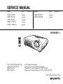
SERVICE MANUAL
MODEL
..............
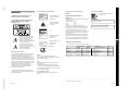
VPL-PS10
VPL-PX10
VPL-PX15
VPLL-CT10
VPLL-CW10
DEST.
.........
CHASSIS NO.
....................
WORLD
WORLD
MODEL
..............
RM-PJM11
RM-PJM15
DEST.
.........
CHASSIS NO.
....................
WORLD
WORLD
WORLD
WORLD
WORLD
REVISED-1
VPL-PS10/PX10/PX15
VPLL-CT10/CW10
RM-PJM11
RM-PJM15
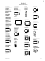
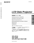
LCD Data Projector
Projection Lens (Not Included)
Remote Commander For VPL-PS10
Remote Commander For VPL-PX10/PX15
LCD DATA PROJECTOR
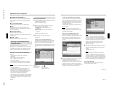
! WARNING
This manual is intended for qualified service personnel only.
To reduce the risk of electric shock, fire or injury, do not perform any servicing other than that
contained in the operating instructions unless you are qualified to do so. Refer all servicing to
qualified service personnel.
! WARNUNG
Die Anleitung ist nur für qualifiziertes Fachpersonal bestimmt.
Alle Wartungsarbeiten dürfen nur von qualifiziertem Fachpersonal ausgeführt werden. Um die
Gefahr eines elektrischen Schlages, Feuergefahr und Verletzungen zu vermeiden, sind bei
Wartungsarbeiten strikt die Angaben in der Anleitung zu befolgen. Andere als die angegeben
Wartungsarbeiten dürfen nur von Personen ausgeführt werden, die eine spezielle Befähigung
dazu besitzen.
! AVERTISSEMENT
Ce manual est destiné uniquement aux personnes compétentes en charge de l’entretien. Afin
de réduire les risques de décharge électrique, d’incendie ou de blessure n’effectuer que les
réparations indiquées dans le mode d’emploi à moins d’être qualifié pour en effectuer d’autres.
Pour toute réparation faire appel à une personne compétente uniquement.
WARNING!!
ATTENTION!!
AN INSULATED TRANSFORMER SHOULD BE USED DURING
ANY SERVICE TO AVOID POSSIBLE SHOCK HAZARD, BECAUSE OF LIVE CHASSIS.
THE CHASSIS OF THIS RECEIVER IS DIRECTLY CONNECTED
TO THE AC POWER LINE.
AFIN D’ÉVITER TOUT RISQUE D’ÉLECTROCUTION
PROVENANT D’UN CHÂSSIS SOUS TENSION, UN
TRANSFORMATEUR D’ISOLEMENT DOIT ETRE UTILISÉ LORS
DE TOUT DÉPANNAGE.
LE CHÂSSIS DE CE RÉCEPTEUR EST DIRECTEMENT
RACCORDÉ Á L’ALIMENTATION SECTEUR.
SAFETY-RELATED COMPONENT WARNING !!
ATTENTION AUX COMPOSANTS RELATIFS Á LA
SÉCURITÉ!!
COMPONENTS IDENTIFIED BY A ! MARK ON THE SCHEMATIC
DIAGRAMS, EXPLODED VIEWS AND IN THE PARTS LIST ARE
CRITICAL TO SAFE OPERATION. REPLACE THESE COMPONENTS WITH SONY PARTS WHOSE PART NUMBERS APPEAR
AS SHOWN IN THIS MANUAL OR IN SUPPLEMENTS PUBLISHED BY SONY.
LES COMPOSANTS IDENTIFIÉS PAR UNE MAPQUE ! SUR
LES SCHÉMAS DE PRINCIPE, LES VUES EXPLOSÉES ET LES
LISTES DE PIECES SONT D’UNE IMPORTANCE CRITIQUE
POUR LA SÉCURITÉ DU FONCTIONNEMENT. NE LES
REMPLACER QUE PAR DES COMPOSANTS SONY DONT LE
NUMÉRO DE PIÈCE EST INDIQUÉ DANS LE PRÉSENT
MANUEL OU DANS DES SUPPLÉMENTS PUBLIÉS PAR SONY.
VPL-PS10/PX10/PX15
CAUTION
ADVARSEL
Danger of explosion if battery is incorrectly replaced.
Lithiumbatteri - Eksplosjonsfare.
Ved utskifting benyttes kun batteri som
anbefalt av apparatfabrikanten.
Brukt batteri returneres
apparatleverandøren.
Replace only with the same or equivalent type
recommended by the manufacturer.
Dispose of used batteries according to the
manufacturer’s instructions.
Vorsicht!
VARNING
Explosionsgefahr bei unsachgemäßem Austausch
der Batterie.
Explosionsfara vid felaktigt batteribyte.
Använd samma batterityp eller en likvärdig typ
som rekommenderas av apparattillverkaren.
Kassera använt batteri enligt gällande
föreskrifter.
Ersatz nur durch denselben oder einen vom
Hersteller empfohlenen ähnlichen Typ. Entsorgung
gebrauchter Batterien nach Angaben des
Herstellers.
ATTENTION
VAROITUS
Il y a danger d’explosion s’il y a remplacement
incorrect de la batterie.
Paristo voi räjähtää jos se on virheellisesti
asennettu.
Vaihda paristo ainoastaan laitevalmistajan
suosittelemaan tyyppiin.
Hävitä käytetty paristo valmistajan ohjeiden
mukaisesti.
Remplacer uniquement avec une batterie du même
type ou d’un type équivalent recommandé par le
constructeur.
Mettre au rebut les batteries usagées conformément
aux instructions du fabricant.
ADVARSEL!
Lithiumbatteri-Eksplosionsfare ved fejlagtig
håndtering.
Udskiftning må kun ske med batteri
af samme fabrikat og type.
Levér det brugte batteri tilbage til leverandøren.
VPL-PS10/PX10/PX15
1 (P)
For the customers in the Netherlands
Voor de klanten in Nederland
Dit apparaat bevat een Li-ion batterij voor memory backup.
Raadpleeg uw leverancier over de verwijdering van de
batterij op het moment dat u het apparaat bij einde
levensduur afdankt.
Gooi de batterij niet weg. maar lever hem in als KCA.
Bij dit product zijn batterijen geleverd.
Wanneer deze leeg zijn, moet u ze niet
weggooien maar inleveren als KCA.
For the customers in the Netherlands
Voor de klanten in Nederland
Bij dit product zijn batterijen geleverd.
Wanneer deze leeg zijn, moet u ze niet
weggooien maar inleveren als KCA.
Für Kunden in Deutschland
Entsorgungshinweis: Bitte werfen Sie nur entladene
Batterien in die Sammelboxen beim Handel oder den
Kommunen. Entladen sind Batterien in der Regel dann,
wenn das Gerät abschaltet und signalisiert “Batterie
leer” oder nach längerer Gebrauchsdauer der Batterien
“nicht mehr einwandfrei funktioniert”. Um
sicherzugehen, kleben Sie die Batteriepole z.B. mit
einem Klebestreifen ab oder geben Sie die Batterien
einzeln in einen Plastikbeutel.
2 (P)
VPL-PS10/PX10/PX15
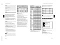
Table of Contents
1. Operating Instructions
1-1.
1-2.
1-3.
1-4.
1-5.
VPL-PX10/PX15/PS10 Operating Instructions .......................................... 1-1
VPL-PX15 Operating Instructions for Networking .................................. 1-25
VPL-PX10/PX15/PS10 Installation Manual ............................................. 1-45
VPLL-CW10 Operating Instructions ........................................................ 1-55
VPLL-CT10 Operating Instructions ......................................................... 1-56
2. Service Informations
2-1.
2-2.
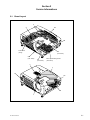
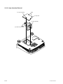
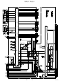
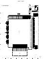
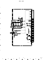
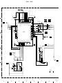
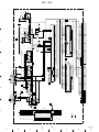
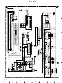
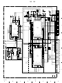
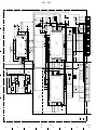
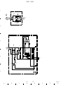
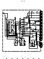
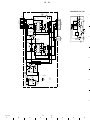
Board Layout ............................................................................................... 2-1
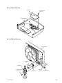
Disassembly ................................................................................................ 2-2
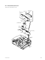
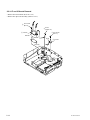
2-2-1. Hood Assembly and Front Assembly Removal ........................ 2-2
2-2-2. H Board Removal ....................................................................... 2-3
2-2-3. NF Board Removal .................................................................... 2-3
2-2-4. C Board Removal ....................................................................... 2-4
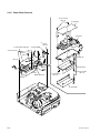
2-2-5. BB and BA Boards Removal ..................................................... 2-5
2-2-6. Power Block Removal ................................................................ 2-6
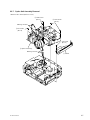
2-2-7. Optics Unit Assembly Removal ................................................. 2-7
2-2-8. GA Board Removal (VPL-PX15 only) ...................................... 2-8
2-2-9. CE block Removal (VPL-PX15 only) ........................................ 2-9
2-2-10. QC and CM Boards Removal (VPL-PX15 only) ..................... 2-10
2-2-11. Parts from the QC Board Removal (VPL-PX15 only) ............. 2-11
2-2-12. QA Board Removal .................................................................. 2-12
2-2-13. QB Board Removal .................................................................. 2-13
2-2-14. F and V Boards Removal ......................................................... 2-14
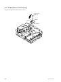
2-2-15. Prism Block Assembly and Polarizer Removal ....................... 2-15
2-2-16. Lamp Assembly Removal ........................................................ 2-16
2-2-17. Extension Boards and Extension Cables Connection .............. 2-17
2-2-18. VPL-PX15 Tool for Writing Network Software ...................... 2-18
2-2-19. Power Cord ............................................................................... 2-19
2-2-20. Main soft and Pixel works soft writing .................................... 2-20
3. Electrical Adjustments
3-1.
3-2.
3-3.
VPL-PS10/PX10/PX15
Preparations ................................................................................................. 3-1
3-1-1. Equipment Required ................................................................... 3-1
3-1-2. How to Enter and Use the Factory Mode ................................... 3-1
V-COM Adjustment .................................................................................... 3-1
Adjustment Item Initialize Data .................................................................. 3-2
1
3-4.
3-5.
3-6.
Service Kowhow ....................................................................................... 3-10
3-4-1. After Replacing the Prism Block ............................................. 3-10
3-4-2. After Replacing the Board ....................................................... 3-10
3-4-2-1. When Replacing the BA Board ................................................ 3-10
3-4-2-2. When Replacing the C Board ................................................... 3-10
3-4-2-3. When Replacing the Other Board ............................................ 3-10
White Balance Adjustment ....................................................................... 3-11
3-5-1. Signal Level Adjustment .......................................................... 3-11
3-5-2. White Balance Adjustment ...................................................... 3-11
3-5-2-1. HIGH Mode of INPUT-A ........................................................ 3-11
3-5-2-2. LOW Mode of INPUT-A ......................................................... 3-11
3-5-2-3. LOW Mode of VIDEO ............................................................. 3-11
Memory ..................................................................................................... 3-12
4. Semiconductors ................................................................................. 4-1
5. Spare Parts
5-1.
5-2.
5-3.
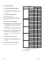
Notes on Repair Parts .................................................................................. 5-1
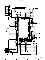
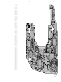
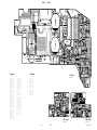
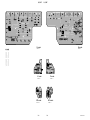
Exploded Views .......................................................................................... 5-2
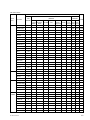
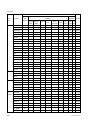
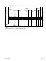
Electrical Parts List ................................................................................... 5-10
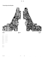
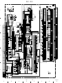
6. Block Diagrams
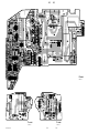
Overall .................................................................................................... 6-1
BA, BB (1/5), QA (1/2) ............................................................................ 6-2
BB (2/5), (3/5), NF, QA (2/2), QB ........................................................... 6-3
BB (4/5), H, V ........................................................................................... 6-4
BB (5/5) .................................................................................................... 6-5
C ............................................................................................................... 6-6
F, G, GA .................................................................................................... 6-7
7. Diagrams
7-1.
7-2.
2
Frame Schematic Diagram .......................................................................... 7-2
Frame (1/3) ............................................................................................... 7-2
Frame (2/3) ............................................................................................... 7-3
Frame (3/3) ............................................................................................... 7-4
Schematic Diagrams and Printed Wiring Boards ........................................ 7-5
Schematic Diagrams
QA (1/2) .................................................................................................... 7-6
QA (2/2) .................................................................................................... 7-7
QB (1/3) .................................................................................................... 7-9
VPL-PS10/PX10/PX15
QB (2/3) .................................................................................................. 7-10
QB (3/3) .................................................................................................. 7-11
BA (1/2) .................................................................................................. 7-13
BA (2/2) .................................................................................................. 7-14
BB (1/7) .................................................................................................. 7-18
BB (2/7) .................................................................................................. 7-19
BB (3/7) .................................................................................................. 7-20
BB (4/7) .................................................................................................. 7-21
BB (5/7) .................................................................................................. 7-22
BB (6/7) .................................................................................................. 7-23
BB (7/7) .................................................................................................. 7-24
C (1/5) .................................................................................................... 7-30
C (2/5) .................................................................................................... 7-31
C (3/5) .................................................................................................... 7-32
C (4/5) .................................................................................................... 7-33
C (5/5) .................................................................................................... 7-34
F ............................................................................................................. 7-38
G (1/3) .................................................................................................... 7-38
G (2/3) .................................................................................................... 7-39
G (3/3) .................................................................................................... 7-40
GA .......................................................................................................... 7-41
H ............................................................................................................. 7-43
V ............................................................................................................. 7-43
NF ........................................................................................................... 7-43
Printed Wiring Boards
QA ............................................................................................................ 7-5
QB ............................................................................................................ 7-8
BA .......................................................................................................... 7-12
BB .......................................................................................................... 7-16
C ............................................................................................................. 7-28
G ............................................................................................................. 7-36
GA .......................................................................................................... 7-36
F ............................................................................................................. 7-37
H ............................................................................................................. 7-42
V ............................................................................................................. 7-42
NF ........................................................................................................... 7-42
VPL-PS10/PX10/PX15
3
VPL-PX15/PX10/PS10
LCD Data Projector
GB
Mode d’emploi
FR
Manual de instrucciones
ES
© 2001 Sony Corporation
1-1
Reprinted from the
operating instructions
VPL-PX15
VPL-PX10
VPL-PS10
Section 1
Operating Instructions
Operating Instructions
1-1. VPL-PX10/PX15/PS10 Operating Instructions
VPL-PS10/PX10/PX15
4-083-534-13(1)
1-2
WARNING
For the customers of the VPL-PX15/PX10
LASER RADIATION
DO NOT STARE INTO BEAM
CLASS 2 LASER PRODUCT
To prevent fire or shock hazard, do not
expose the unit to rain or moisture.
RAYONNEMENT LASER
NE PAS REGARDER DANS LE FAISCEAU
APPAREIL A LASER DE CLASSE 2
LASER–STRAHLING,
NICHT IN DEN STRAHL BLICKEN
LASER KLASSE 2
MAX OUTPUT : 1mW
EN60825-1
WAVE LENGTH : 645nm
/A11:1996
To avoid electrical shock, do not open the
cabinet. Refer servicing to qualified
personnel only.
This label is located on
the rear of the Remote
Commander.
CAUTION
LASER RADIATION
DO NOT STARE INTO BEAM
WAVE LENGTH:645nm
MAX OUTPUT:1mW
CLASS II LASER PRODUCT
A
MANUFACTURED
This symbol is intended to alert the
user to the presence of important
operating and maintenance (servicing)
instructions in the literature
accompanying the appliance.
For the customers in the USA
This equipment has been tested and found to comply with
the limits for a Class A digital device, pursuant to Part 15 of
the FCC Rules. These limits are designed to provide
reasonable protection against harmful interference when the
equipment is operated in a commercial environment. This
equipment generates, uses, and can radiate radio frequency
energy and, if not installed and used in accordance with the
instruction manual, may cause harmful interference to radio
communications. Operation of this equipment in a
residential area is likely to cause harmful interference in
which case the user will be required to correct the
interference at his own expense.
You are cautioned that any changes or modifications not
expressly approved in this manual could void your authority
to operate this equipment.
AVOID EXPOSURELASER RADIATION IS
EMITTED FROM THIS
APERTURE.
Gooi de batterij niet weg, maar lever
hem in als KCA.
This label is located on the
rear of the Remote
Commander.
This label is located on the
rear of the Remote
Commander.
IMPORTANT
The wires in this mains lead are coloured in accordance with
the following code:
Green-and-Yellow: Earth
Blue:
Neutral
Brown:
Live
As the colours of the wires in the mains lead of this
apparatus may not correspond with the coloured markings
identifying the terminals in your plug proceed as follows:
The wire which is coloured green-and-yellow must be
connected to the terminal in the plug which is marked by the
letter E or by the safety earth symbol I or coloured green
or green-and-yellow.
The wire which is coloured blue must be connected to the
terminal which is marked with the letter N or coloured black.
The wire which is coloured brown must be connected to the
terminal which is marked with the letter L or coloured red.
Apparaten ma kun tilkoples jordet stikkontakt.
Apparatet må kun tilkoples jordet stikkontakt.
GB
Warning on power connection
Use a proper power cord for your local power supply.
Laser light shines out of this window.
Caution
Use of controls or adjustments or performance of
procedures other than those specified herein may result in
hazardous radiation exposure.
The socket-outlet should be installed near the equipment
and be easily accessible.
English
This symbol is intended to alert the
user to the presence of uninsulated
“dangerous voltage” within the
product’s enclosure that may be of
sufficient magnitude to constitute a risk
of electric shock to persons.
Voor de klanten in Nederland
WARNING
THIS APPARATUS MUST BE EARTHED
This label is located on
the rear of the Remote
Commander.
COMPLIES WITH DHHS 21 CFR
SUBCHAPTER J
SONY CORPORATION
6-7-35 KITASHINAGAWA
SHINAGAWA-KU, TOKYO, JAPAN
For the customers in the United Kingdom
The United States,
Canada
Continental
Europe
UK, Ireland,
Australia, New Zealand
Plug type
VM0233
290B
YP-12A
COX-07
—1)
YP332
Female end
VM0089
386A
YC-13B
COX-02
VM0310B
YC-13
Japan
Cord type
SJT
SJT
H05VV-F H05VV-F
Rated Voltage & Current
10A/125V
10A/125V
10A/250V 10A/250V 10A/250V
7A/125V
Safety approval
UL/CSA
UL/CSA
VDE
DENAN
VDE
N13237/CO-228
VDE
VCTF
Notes
• Do not aim the laser at people and do not look into the
laser transmitter.
• If the Remote Commander malfunctions or causes a
malfunction, consult with qualified Sony personnel. We will
exchange the Remote Commander for a new one based
on the terms of the guarantee.
For the customers in Canada
This Class A digital apparatus complies with Canadian
ICES-003.
VPL-PS10/PX10/PX15
.........................................................................................................................................................................................................
1) Use the correct plug for your country.
2 (GB)
3 (GB)
VPL-PS10/PX10/PX15
Table of Contents
Overview
Precautions ............................................................... 7 (GB)
Features ..................................................................... 8 (GB)
Location and Function of Controls ......................... 9 (GB)
Front / Left Side ....................................................... 9 (GB)
Rear / Right Side / Bottom ....................................... 9 (GB)
Control Panel ......................................................... 11 (GB)
Connector Panel ..................................................... 13 (GB)
Remote Commander (supplied with the
VPL-PX15/PX10) ............................................. 14 (GB)
Remote Commander (supplied with the
VPL-PS10) ........................................................ 16 (GB)
Setting Up and Projecting
Installing the Projector ........................................... 18 (GB)
Connecting the Projector ....................................... 18 (GB)
Connecting to a Computer ..................................... 18 (GB)
Connecting to a VCR or 15k RGB/Component
Equipment ......................................................... 20 (GB)
Connecting to a LAN (VPL-PX15 only) ............... 21 (GB)
Selecting the Menu Language ............................... 23 (GB)
Projecting ................................................................ 24 (GB)
Adjustments and Settings Using the Menu
Using the Menu ....................................................... 27 (GB)
The PICTURE CTRL Menu ..................................... 28 (GB)
The INPUT SETTING Menu .................................... 29 (GB)
The SET SETTING Menu ........................................ 31 (GB)
The INSTALL SETTING Menu ................................ 32 (GB)
Installation
Installation Example ............................................... 34 (GB)
Notes for Installation .............................................. 35 (GB)
Unsuitable Installation ........................................... 35 (GB)
Unsuitable Conditions for Use ............................... 35 (GB)
4 (GB)
5 (GB)
1-3
1-4
Precautions
Maintenance ............................................................ 37 (GB)
Precautions
Replacing the Lamp ............................................... 37 (GB)
Cleaning the Air Filter ........................................... 38 (GB)
Troubleshooting ..................................................... 39 (GB)
Other
Specifications ......................................................... 41 (GB)
Index ........................................................................ 44 (GB)
On safety
• Check that the operating voltage of your unit is
identical with the voltage of your local power
supply.
• Should any liquid or solid object fall into the cabinet,
unplug the unit and have it checked by qualified
personnel before operating it further.
• Unplug the unit from the wall outlet if it is not to be
used for several days.
• To disconnect the cord, pull it out by the plug. Never
pull the cord itself.
• The wall outlet should be near the unit and easily
accessible.
• The unit is not disconnected to the AC power source
(mains) as long as it is connected to the wall outlet,
even if the unit itself has been turned off.
• Do not look into the lens while the lamp is on.
• Do not aim the laser at people and do not look into
the laser transmitter.
• Do not place your hand or objects near the
ventilation holes — the air coming out is hot.
• Be careful not to catch your fingers with the
adjusters when you lift up the projector. Do not push
hard on the top of the projector with the adjusters
out.
• Be sure to grasp both sides when carrying the
projector.
On illumination
• To obtain the best picture, the front of the screen
should not be exposed to direct lighting or sunlight.
• Ceiling-mounted spot lighting is recommended. Use
a cover over fluorescent lamps to avoid lowering the
contrast ratio.
• Cover any windows that face the screen with opaque
draperies.
• It is desirable to install the projector in a room where
floor and walls are not of light-reflecting material. If
the floor and walls are of reflecting material, it is
recommended that the carpet and wall paper be
changed to a dark color.
VPL-PS10/PX10/PX15
6 (GB)
On preventing internal heat build-up
After you turn off the power with the I / 1 key on the
Remote Commander or on the control panel, do not
disconnect the unit from the wall outlet while the
cooling fan is still running.
Caution
The projector is equipped with ventilation holes
(intake) on the bottom and ventilation holes (exhaust)
on the front. Do not block or place anything near these
holes, or internal heat build-up may occur, causing
picture degradation or damage to the projector.
On cleaning
• To keep the cabinet looking new, periodically clean
it with a soft cloth. Stubborn stains may be removed
with a cloth lightly dampened with a mild detergent
solution. Never use strong solvents, such as thinner,
benzene, or abrasive cleansers, since these will
damage the cabinet.
• Avoid touching the lens. To remove dust on the lens,
use a soft dry cloth. Do not use a damp cloth,
detergent solution, or thinner.
• Clean the filter at regular intervals, every 300 hours.
On repacking
Save the original shipping carton and packing
material; they will come in handy if you ever have to
ship your unit. For maximum protection, repack your
unit as it was originally packed at the factory.
About the LCD projector
The LCD projector is manufactured using highprecision technology. You may, however, see tiny
black points and/or bright points (red, blue, or green)
that continuously appear on the LCD projector. This is
a normal result of the manufacturing process and does
not indicate a malfunction.
7 (GB)
Overview
Maintenance
• High brightness
Adopting a newly developed optical system and a 200
W UHP lamp allows high brightness (VPL-PX15/
PX10: light output 2000 ANSI lumen, VPL-PS10:
light output 1500 ANSI lumen) and excellent
uniformity on the picture.
• High resolution
VPL-PX15/PX10
Three 0.9-inch, approximately 790,000 pixel, XGA
panels provide a resolution of 1024 × 768 dots for
RGB input and 750 horizontal TV lines for video
input.
VPL-PS10
Three 0.9-inch, approximately 480,000 pixel, SVGA
panels provide a resolution of 800 × 600 dots for RGB
input and 600 horizontal TV lines for video input.
Simple setup
• Simple setup with external equipment
The projector has 37 preset data items for input
signals in memory, which allows you to project a
clear picture on the screen simply by connecting
equipment and pressing the APA (Auto Pixel
Alignment) key.
• Compatible with USB (Universal Serial Bus) hub
functions
You can connect USB equipment (e.g., a USB mouse)
to the projector, and also control the projector by
using the “Projector Station” application software
(CD-ROM) supplied with the projector from a
computer operated with Microsoft1) Windows1) 98,
Windows 98 SE or Windows 2000. Using this
application software, you can open a file you want to
use for your presentation with the supplied Remote
Commander.
• Digital zoom / freeze functions
This projector has a digital zoom function that enables
you to enlarge the image at a desired location on the
screen. The freeze function allows you to freeze the
picture projected. The frozen picture continues to be
projected even if the equipment is disconnected from
the video source.
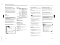
Location and Function of
Controls
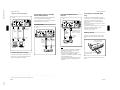
Front / Left Side
4 Ventilation holes (exhaust)
q;
5 Lens
Remove the lens cap before projection.
1
2
3
6 Adjuster buttons
Accepts various input signals
• Compatible with six color systems
Any of the NTSC3.58, PAL, SECAM, NTSC4.433), PALM, or PAL-N color systems can be selected
automatically or manually.
2 Focus ring
Adjusts the picture focus.
3 Front remote control detector
qa
4
• Scan converter loaded
This projector has a built-in scan converter that
converts the input signal to 1024 × 768 dots (VPLPX15/PX10) or 800 × 600 dots (VPL-PS10).
• Compatible input signals
This projector accepts composite, S video, and
component video signals as well as 15k RGB, VGA2),
SVGA2), XGA2), and SXGA2) signals, which can all be
displayed.
1 Zoom ring
Adjusts the size of the picture.
5
6
89
7 Handle release
Push to make the carrying handle 0 pop up.
8 Connector panel
7
For details, see “Connector Panel” on page 13 (GB).
9 Connector panel cover
If necessary, open this cover to use the connectors on
the connector panel. You can remove the cover by
releasing the connector panel cover lock qf.
(This illustration shows the VPL-PX15.)
Left side
Rear / Right Side / Bottom
PUSH
High brightness, high picture quality
Easy presentation
• Multi functional Remote Commander with mouse
control functions
You can operate a computer connected to this
projector with the Remote Commander since the unit
has a built-in mouse receiver.
PUSH
Features
PUSH
VPL-PS10/PX10/PX15
Location and Function of Controls
Features
Other functions
• Networking compatibility (Wireless compatible,
VPL-PX15 only)
The projector has the Microsoft Windows CE
operating system built in and is equipped with a PC
CARD slot and ETHER connector, which allows you
to connect the unit to a wired or wireless LAN.
qd qs
ws ql wa w; ql qk
qj
Connector panel cover
q; Carrying handle
Use the handle release 7 to make the handle pop up
from the projector for carrying.
qa Control panel
For information on the networking function of this
projector, refer to the Operating Instructions for
Networking supplied with the unit.
For details, see “Control Panel” on page 11 (GB).
qs Rear remote control detector
qf
qg
qh
qd Left speaker
.........................................................................................................................................................................................................
1) Microsoft and Windows are registered trademarks of Microsoft Corporation (U.S.A. and other countries).
2) VGA, SVGA, XGA and SXGA are registered trademarks of the International Business Machines Corporation, U.S.A.
3) NTSC4.43 is the color system used when playing back a video recorded on NTSC on an NTSC4.43 system VCR.
8 (GB)
9 (GB)
1-5
1-6
Location and Function of Controls
Location and Function of Controls
qf Connector panel cover lock
Used to remove/install the connector panel cover 9.
Bottom
2
wa Air filter cover lock
Used to remove the air filter cover.
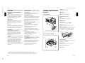
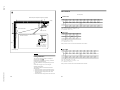
How to use the adjusters
For details, see “Cleaning the Air Filter” on page 38 (GB).
To adjust the height
Note
Clean the air filter every 300 hours to ensure
optimal performance.
1
While pressing both sides of the lock, slide the
connector cover outward to release it.
LAMP/
COVER
Adjust the height of the projector as follows:
1
ws Ventilation holes (intake) / air filter cover
1
Control Panel
Lift the projector and press the adjuster buttons.
The adjusters will extend from the projector.
VOLUME
Notes
1
• Do not place anything near the ventilation holes as it
may cause internal heat build-up.
• Do not place your hand or objects near the
ventilation holes — the air coming out is hot.
qg Rear adjusters
qh Adjusters
When a picture is projected on an exterior of the
screen, adjust the picture using these adjusters.
Adjuster buttons
2
For details on how to use the adjusters, see “How to use
the adjusters” on page 11 (GB).
qj Security lock
Connects to an optional security cable (made by
Kensington)1).
POWER
ON/
SAVING STANDBY
MENU
RESET
ENTER
q;
9
INPUT
2 3 4 5 6 7 8
1 HELP key
If you need help information during an operation,
press this key to display help messages. The Help
menu lists error recovery techniques depending on
problem type.
2 VOLUME +/– keys
Adjust the volume of the built-in speakers.
+ : Increases the volume.
– : Decreases the volume.
3 APA (Auto Pixel Alignment) key
Adjusts the picture to be projected automatically to
give the clearest picture possible while a signal from
the computer is input. Adjusts the shift (up/down and
left/right) at the same time automatically.
The security lock corresponds to Kensington’s
MicroSaver ®1) Security System.
If you require further information, contact
Kensington
2855 Campus Drive, San Mateo, CA 94403
Note
Note
If the adjusters have been extended to the limit
and you keep turning the adjusters
counterclockwise, the adjusters will stop turning
and the adjuster buttons cannot be pressed. In this
case, turn the adjusters clockwise, and then press
the adjuster buttons again.
In North America
Phone: 800-235-6708
Fax: 800-247-1317
Outside North America
Phone: 847-541-9500
Home page address:
http://www.kensington.com/
While pressing the buttons, adjust the height.
Then, release the buttons.
The adjusters will lock, then the height of the
projector will be fixed. For fine adjustment, turn
the adjusters to the right or left.
APA
TEMP/
FAN
HELP
3
If necessary, turn the rear adjusters to the right or
left to adjust the height of the projector.
Press the APA key when the full image is displayed
on the screen. If there are black edges around the
image, the APA function will not function properly
and the image may extend beyond the screen.
4 RESET key
Resets the value of an item to its factory preset value.
This key functions when the menu or a setting item is
displayed on the screen.
5 Arrow (M/m/</,) keys
Used to select a menu or to make various adjustments.
qk Lamp cover
6 ENTER key
Enters the settings of items in the menu system.
ql Ventilation holes (intake)
w; Right speaker
Notes
VPL-PS10/PX10/PX15
.........................................................................................................................................................................................................
1) Kensington and MicroSaver are registered trademarks of Kensington Technology Group.
10 (GB)
• Be careful not to let the projector down on your
fingers.
• Do not push hard on the top of the projector with the
adjusters out.
11 (GB)
7 INPUT key
Selects the input signal. Each time you press the key,
the input signal switches as follows:
INPUT-A
S-VIDEO
INPUT-B (VPL-PX15 only)
VIDEO
Notes
• You can select INPUT-B only if INPUT-B FUNC. in
the INSTALL SETTING menu has been set to ON.
INPUT-B is only available for the VPL-PX15.
• The audio signals are the same for the VIDEO and
S-VIDEO.
• The audio signals are the same for the INPUT-A and
INPUT-B.
8 I / 1 (on / standby) key
Turns the projector on and off when the projector is in
the standby mode. The ON/STANDBY indicator
lights in green when the power is turned on.
When turning off the power, press the I / 1 key
twice following the message on the screen, or press
and hold the key for about one second.
For details on steps for turning off the power, see “To turn
off the power” on page 25 (GB).
9 MENU key
Displays the on-screen menu. Press again to clear the
menu.
0 Indicators
LAMP/COVER: Lights up or flashes under the
following conditions:
• Lights up when the lamp has reached the end of
its life or has reached a high temperature.
• Flashes when the lamp cover or air filter cover
is not secured firmly.
TEMP (Temperature)/FAN: Lights up or flashes
under the following conditions:
• Lights up when temperature inside the projector
becomes unusually high.
• Flashes when the fan is broken.
12 (GB)
Location and Function of Controls
POWER SAVING: Lights up when the projector is
in the power saving mode. When POWER
SAVING in the SET SETTING menu is set to
ON, the projector goes into the power saving
mode if no signal is input for 10 minutes.
Although the lamp goes out, the cooling fan
keeps running. The power saving mode is
canceled when a signal is input or any key is
pressed. However, in the power saving mode,
none of the keys function for the first 60 seconds.
ON/STANDBY: Lights up or flashes under the
following conditions:
• Lights up in red when the AC power cord is
plugged into the wall outlet. Once in the
standby mode, you can turn on the projector
with the I / 1 key.
• Lights up in green when the power is turned on.
• Flashes in green while the cooling fan runs after
the power is turned off with the I / 1 key. The
fan runs for about 90 seconds after turning off
the power.
The ON/STANDBY indicator flashes quickly
for the first 60 seconds of that time.
During this first 60 seconds, you cannot turn the
power back on with the I / 1 key.
For details on the LAMP/COVER and the TEMP/FAN
indicators, see page 40 (GB).
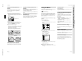
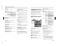
Connector Panel
4 INPUT B connectors (VPL-PX15 only)
INPUT B PC CARD slot (Type II): A wireless
LAN PC card or PC memory card can be installed
according to your requirements.
Left side
For details, see “Installing a PC card” on page 21 (GB).
INPUT B ETHER connector (10BASE-T/
100BASE-TX): Connects to a computer on a
LAN with a LAN cable when you use the
networking function of this projector.
PUSH
VPL-PS10/PX10/PX15
Location and Function of Controls
INPUT B
PC CARD
AUDIO
MOUSE
VIDEO S VIDEO
PLUG IN POWER
CTRL S
AUDIO
INPUT A
~AC IN
56 7
INPUT B
PC CARD
8
AUDIO
MOUSE
VIDEO S VIDEO
PLUG IN POWER
CTRL S
4
3
AUDIO
INPUT A
~AC IN
2
5 MOUSE connector (6-pin)
Connects to the PS/2 mouse port on a computer via
the supplied mouse cable, to control the mouse
function of the connected computer.
1
(This illustration shows the VPL-PX15.)
1 AC IN socket
Connects the supplied AC power cord.
2 INPUT A connectors
Connect to external equipment such as a computer.
INPUT A connector (HD D-sub 15-pin, female):
Connects to the monitor output on a computer
using the supplied cable.
When inputting a component or 15k RGB signal,
use the appropriate cable.
For details, see “To connect 15k RGB/Component
equipment” on page 21 (GB).
AUDIO jack (stereo minijack): Connects to the
audio output of the computer.
3 CTRL S /PLUG IN POWER (DC 5V output)
jack (stereo minijack)
Connects to the control S out jack of Sony equipment.
Connects to the CONTROL S OUT jack on the
supplied Remote Commander to use it as a wired
remote control unit. In this case, you do not need to
install batteries in the Remote Commander, since the
power is supplied from this jack.
6 USB connector (USB B-plug for upstream, 4pin)
Connects to a computer. When you connect the
projector to the computer via this connector, the
projector recognizes that a USB mouse is connected
and you can control the mouse function of the
computer connected to the INPUT A connector using
the supplied Remote Commander. The supplied
application software can be used on the computer
connected to this connector.
7 USB connector (USB A-plug for downstream, 4pin)
Connects to USB equipment such as a mouse, camera,
etc.
8 Video input connectors
Connect to external video equipment such as a VCR.
S VIDEO connector (mini DIN 4-pin): Connects to
the S video output (Y/C video output) of video
equipment.
VIDEO jack (phono type): Connects to the
composite video output of video equipment.
AUDIO jack (stereo minijack): Connects to the
audio output of the VCR.
13 (GB)
1-7
1-8
Location and Function of Controls
Location and Function of Controls
Remote Commander (supplied with
the VPL-PX15/PX10)
Keys which have the same names as those on the
control panel function identically.
wg
wf
wd
ws
wa
w;
ql
qk
COMMAND
OFF ON
PIC
PJ NETWORK MUTING
AUDIO
INPUT
D KEYSTONE
HELP
VOLUME
APA
FREEZE
MENU/
TAB
LASER
qj
qh
qg
qf
ENTER
R
CLICK
RESET/
ESCAPE
D ZOOM
1
2
3
1
2
3
4
5
6
7
8
9
q;
qa
FUNCTION
RM-PJM15
PROJECTOR
qs,qd
Notes on the laser beam
• Do not look into the laser transmitter.
• Do not aim the laser at people.
1 I / 1 (on / standby) key
2 MUTING keys
Cut off the picture and sound.
PIC: Cuts off the picture. Press again to restore the
picture.
AUDIO: Cuts off the sound from the speakers. Press
again or press the VOLUME + key to restore the
sound.
7 Mouse
When the PJ/NETWORK select switch is set to
PJ: Functions as the mouse of the computer
connected to this projector.
When the PJ/NETWORK select switch is set to
NETWORK (VPL-PX15 only): Functions as the
mouse in the INPUT B window of this projector.
8 Arrow (M/m/</,) keys
9 R (right) CLICK key
When the PJ/NETWORK select switch is set to
PJ: Functions as the right button of the mouse of
the computer connected to this projector.
When the PJ/NETWORK select switch is set to
NETWORK (VPL-PX15 only): Functions as the
right button of the mouse in the INPUT B
window of this projector.
0 ENTER key
qa FUNCTION 1, 2, 3 keys
When the PJ/NETWORK select switch is set to
PJ: Functions when the supplied application
software is used. When you connect the projector
with a computer, you can open a file on the
screen by just pressing a FUNCTION key. This
will enhance your presentation. To use this
function, allocate a file to the FUNCTION key by
using the application software. (Only the
FUNCTION 1 and 2 keys are available. You
cannot allocate a file to the FUNCTION 3 key.)
For details, see the README file and HELP file supplied
with the application software.
When the PJ/NETWORK select switch is set to
NETWORK (VPL-PX15 only): When the
INPUT B window is displayed on the projector,
you can start an application by just pressing a
FUNCTION key. To use this function, allocate an
application to a FUNCTION key. (The
FUNCTION 3 key is allocated to the keyboard
software display.)
qs Strap holder
Attaches the supplied strap.
3 INPUT key
4 D KEYSTONE key
Corrects the trapezoidal distortion caused by the
projection angle. Use the arrow keys (M/m/</,) to
display the image as a rectangle.
5 FREEZE key
Used to freeze the picture projected. To cancel the
frozen picture, press the key again.
VPL-PS10/PX10/PX15
6 LASER key
Emits a laser beam from the laser transmitter while
you keep this key pressed.
14 (GB)
qd CONTROL S OUT jack (stereo minijack)
Connects to the CTRL S jack on the projector with the
connecting cable (not supplied) to use the Remote
Commander as a wired remote control unit. In this
case, you do not need to install batteries in the Remote
Commander since the power is supplied via the CTRL
S jack on the projector.
qf RESET/ESCAPE key
When the PJ/NETWORK select switch is set to
PJ: Functions as the RESET key.
When the PJ/NETWORK select switch is set to
NETWORK (VPL-PX15 only): Functions as the
ESCAPE key of the keyboard when the INPUT B
window is displayed.
qg D ZOOM +/– key
Enlarges the image at a desired location on the screen.
This key works only when a signal from a computer is
input.
+: Pressing the + key once displays the icon. This
icon indicates the point you want to enlarge. Use
an arrow key (M/m/</,) to move the icon to
the point to be enlarged. Press the + key
repeatedly until the image is enlarged to meet
your requirements.
–: Each press of the – key reduces an image that has
been enlarged with the D ZOOM + key.
wd Transmission indicator
Lights up when you press a key on the Remote
Commander.
This indicator does not light up when you use the laser
pointer.
wf Infrared transmitter
wg Laser transmitter
qh L (left) CLICK key
When the PJ/NETWORK select switch is set to
PJ: Functions as the left button of the mouse of
the computer connected to this projector.
When the PJ/NETWORK select switch is set to
NETWORK (VPL-PX15 only): Functions as the
left button of the mouse in the INPUT B window
of this projector.
qj MENU/TAB key
When the PJ/NETWORK select switch is set to
PJ: Functions as the MENU key.
When the PJ/NETWORK select switch is set to
NETWORK (VPL-PX15 only): Functions as the
TAB key of the keyboard when the INPUT B
window is displayed.
qk APA (Auto Pixel Alignment) key
ql VOLUME +/– keys
w; HELP key
If you need help information during an operation,
press this key to display help messages.
wa PJ/NETWORK select switch
To use the Remote Commander for network
operations, set the switch to NETWORK. Set the
switch to PJ to use the Remote Commander for
normal operations other than networking. This switch
is only available for the VPL-PX15.
For details on the operation of the Windows CE screen, see
the supplied “Operating Instructions for Networking.”
ws COMMAND ON/OFF switch
When this switch is set to OFF, no keys on the
Remote Commander will function. This saves battery
power.
15 (GB)
VPL-PS10/PX10/PX15
Location and Function of Controls
Location and Function of Controls
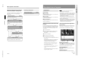
Battery installation
1
Push and slide to open the lid, then install the two
R6 (size AA) batteries (supplied) with the correct
polarity.
Remote Commander (supplied with
the VPL-PS10)
Keys which have the same names as those on the
control panel function identically.
4
5
9 D ZOOM +/– key
Enlarges the image at a desired location on the screen.
This key works only when a signal from a computer is
input.
+: Pressing the + key once displays the icon. This
icon indicates the point you want to enlarge. Use
an arrow key (M/m/</,) to move the icon to
the point to be enlarged. Press the + key
repeatedly until the image is enlarged to meet
your requirements.
–: Each press of the – key reduces an image that has
been enlarged with the D ZOOM + key.
6
0 L (left) CLICK key
Functions as the left button of a mouse.
7
qa MENU key
Slide while pressing
down on the lid.
Be sure to install
the battery from
the # side.
2
Replace the lid.
Notes on batteries
• Make sure that the battery orientation is correct when
inserting batteries.
• Do not mix an old battery with a new one, or
different types of batteries.
• If you do not intend to use the Remote Commander
for a long time, remove the batteries to avoid damage
from battery leakage. If batteries have leaked,
remove them, wipe the battery compartment dry and
replace the batteries with new ones.
Notes on Remote Commander operation
• Make sure that there is nothing to obstruct the
infrared beam between the Remote Commander and
the remote control detector on the projector.
• The operation range is limited. The shorter the
distance between the Remote Commander and the
projector is, the wider the angle within which the
commander can control the projector.
qh
qg
qf
qd
qs
qa
FREEZE MS SLIDE I / 1
D KEYSTONE
INPUT
APA
MENU
ENTER
9
8
1
2
3
q;
+
–
RESET
R
CLICK
8 RESET key
Resets the value of an item to its factory preset value
or returns the enlarged image back to its original size.
D ZOOM
1 FUNCTION
2
qs D KEYSTONE key
Corrects the trapezoidal distortion caused by the
projection angle. Use the arrow keys (M/m/</,) to
display the image as a rectangle.
qd INPUT key
1 I / 1 (on / standby) key
2 APA (Auto Pixel Alignment) key
qf FREEZE key
Used to freeze the picture projected. To cancel the
frozen picture, press the key again.
qg MS SLIDE key
This key does not operate with this unit.
Battery installation
1
Push and slide to open the lid, then install the two
R6 (size AA) batteries (supplied) with the correct
polarity.
Slide while pressing
down on the lid.
Be sure to install
the battery from
the # side.
2
Replace the lid.
Notes on batteries
• Make sure that the battery orientation is correct when
inserting batteries.
• Do not mix an old battery with a new one, or
different types of batteries.
• If you do not intend to use the Remote Commander
for a long time, remove the batteries to avoid damage
from battery leakage. If batteries have leaked,
remove them, wipe the battery compartment dry and
replace the batteries with new ones.
Notes on Remote Commander operation
• Make sure that there is nothing to obstruct the
infrared beam between the Remote Commander and
the remote control detector on the projector. Direct
the Remote Commander toward the front or rear
remote control detector.
• The operation range is limited. The shorter the
distance between the Remote Commander and the
projector is, the wider the angle within which the
commander can control the projector.
3 ENTER key
qh Infrared transmitter
4 Joystick
Functions as the mouse of the computer connected to
this projector.
5 Arrow (M/m/</,) keys
6 R (right) CLICK key
Functions as the right button of a mouse.
7 FUNCTION 1, 2 keys
Functions when the supplied application software is
used. When you connect the projector with a
computer, you can open a file on the screen by just
pressing a FUNCTION key. This will enhance your
presentation. To use this function, allocate a file to the
FUNCTION key by using the application software.
For details, see the README file and HELP file supplied
with the application software.
16 (GB)
17 (GB)
1-9
Connecting the Projector
Connecting the Projector
This section describes how to install the projector.
The distance between the lens and the screen varies
depending on the size of the screen. Use the following
table as a guide.
When making connections, be sure to do the
following:
• Turn off all equipment before making any
connections.
• Use the proper cables for each connection.
• Insert the cable plugs properly; plugs that are not
fully inserted often generate noise or cause picture
degradation. When pulling out a cable, be sure to
pull it out grasping the plug, not the cable itself.
To connect an IBM1) PC/AT1) compatible
computer
When you use a USB mouse and USB
equipment
Left side
to USB
equipment
Connecting to a Computer
This section describes how to connect the projector to
a computer.
For more information, refer to the computer’s
instruction manual.
Distance between the screen
and the center of the lens
AUDIO
MOUSE
VIDEO S VIDEO
PLUG IN POWER
CTRL S
AUDIO
INPUT A
Notes
Unit: m (feet)
40
60
80
100
120
150
Recommended operating environment
When you use the USB function, connect your
computer as illustrated in the box on the left.
This application software and the USB function can
be used on a computer loaded with Windows 98,
Windows 98 SE or Windows 2000.
~AC IN
Notes
Screen
size
(inches)
On the USB function
When connecting the projector to a computer using
the USB cable for the first time, the computer
recognizes the following devices automatically.
1 USB hub (general use)
2 USB human interface device (wireless mouse
function)
3 USB human interface device (projector control
function)
The computer also recognizes the device connected to
the downstream connector on the projector.
180
200
250
300
Minimum 1.5 2.2 3.0 3.7 4.5 5.6 6.8 7.5 9.4 11.3
Distance (4.8) (7.3) (9.8) (12.3) (14.8) (18.5) (22.3) (24.8) (31.0) (37.3)
Maximum 1.8 2.7 3.6 4.5 5.4 6.8 8.1 9.1 11.3 13.6
Distance (5.8) (8.8) (11.8) (14.8) (17.8) (22.2) (26.7) (29.7) (37.2) (44.7)
For details, see “Installation Example” on page 34 (GB).
For details on ceiling installation, consult with qualified
Sony personnel (fee charged).
• The projector accepts VGA, SVGA, XGA, and
SXGA signals. However, we recommend that you
set the output mode of your computer to SVGA
(VPL-PS10) or XGA (VPL-PX15/PX10) mode for
the external monitor.
• If you set your computer, such as a notebook type, to
output the signal to both your computer’s display and
an external monitor, the picture of the external
monitor may not appear properly. Set your computer
to output the signal to only the external monitor.
Stereo
audio
connecting
cable (not
supplied)
USB cable
A type – B
type
(supplied)
HD D-sub 15-pin
cable (supplied)
to audio
output
to USB
connector
to monitor
output
For details, refer to the operating instructions supplied
with your computer.
• The supplied mouse cable may not work properly
depending on your computer.
• This projector is compatible with DDC2B (Display
Data Channel 2B). If your computer is compatible
with DDC1), turn the projector on according to the
following procedures.
1
Connect the projector to the computer using the
supplied HD D-sub 15-pin cable.
2
3
Turn the projector on.
• As the projector recognizes the USB mouse when
the computer is connected to the USB connector, do
not connect anything to the MOUSE connector.
• Your computer may not start correctly when
connected to the projector via the USB cable. In this
case, disconnect the USB cable, restart the computer,
then connect the computer to the projector using the
USB cable.
• This projector is not guaranteed for suspend or
standby mode. When you use the projector in
suspend or standby mode, disconnect the projector
from the USB port on the computer.
• Operations are not guaranteed for all the
recommended computer environments.
Computer
Start the computer.
VPL-PS10/PX10/PX15
.........................................................................................................................................................................................................
.........................................................................................................................................................................................................
1) DDC™ is a registered trademark of the Video Electronics Standards Association.
1) IBM® and PC/AT are a trademark and a registered trademark of International Business Machines Corporation, U.S.A.
18 (GB)
19 (GB)
Setting Up and Projecting
Installing the Projector
PUSH
1-10
Installing the Projector / Connecting the Projector
VPL-PS10/PX10/PX15
Connecting the Projector
Connecting the Projector
When you use a PS/2 mouse port
Left side
AUDIO
MOUSE
VIDEO S VIDEO
Connecting to a VCR or 15k RGB/
Component Equipment
This section describes how to connect the projector to
a VCR or 15k RGB/component equipment.
For more information, refer to the instruction manuals
of the equipment you are connecting.
To connect 15k RGB/Component
equipment
Left side
CTRL S
AUDIO
MOUSE
PLUG IN POWER
AUDIO
INPUT A
VIDEO S VIDEO
PLUG IN POWER
To connect a VCR
~AC IN
CTRL S
AUDIO
INPUT A
~AC IN
Left side
PS/2
Mouse
cable
(supplied)
Stereo
audio
connecting
cable (not
supplied)
HD D-sub 15-pin
cable (supplied)
AUDIO
MOUSE
VIDEO S VIDEO
to monitor
output
Computer
AUDIO
INPUT A
~AC IN
to audio
output
Stereo
audio
connecting
cable (not
supplied)
to audio
output
SMF-402 Signal Cable (not
supplied) HD D-sub 15-pin
(male) y 3 × phono jack
Video
cable (not
supplied)
to RGB/
component
output
S-Video
cable (not
supplied)
Installing a PC card
When you use a wireless LAN PC card or memory
card, insert the card into the INPUT B PC CARD
slot.
The eject button pops out
when the card is inserted.
15k RGB/Component
equipment
to video
output
to S video
output
PUSH
CTRL S
to audio
output
This projector is networking compatible. Using a
wireless LAN PC card or a 10BASE-T/100BASE-TX
LAN cable, you can connect the projector to a
wireless or wired LAN. You can also install a PC
memory card.
This section describes how to connect to a LAN and
how to install a PC card.
Whenever you connect the projector to a LAN or use
a memory card, set INPUT-B FUNC. in the
INSTALL SETTING menu to ON.
For details, see page 33 (GB).
Stereo
audio
connecting
cable (not
supplied)
PLUG IN POWER
to mouse
port (PS/2)
Connecting to a LAN (VPL-PX15
only)
Notes
• Set the aspect ratio using ASPECT in the INPUT
SETTING menu according to the input signal.
To connect a Macintosh1) computer
VCR
Use an ADP-20 signal adapter (not supplied). In this
case, however, you cannot control the mouse of the
computer using the Remote Commander.
PC card
For details, see page 30 (GB).
• When you connect the projector to 15k RGB/
component video equipment, select RGB,
component or VCR GBR with the INPUT-A setting
in the SET SETTING menu.
• Use the composite sync signal when you input the
external sync signal from 15k RGB/component
equipment.
Insert the card with the arrow mark
facing toward the slot.
To remove the PC card from the slot, press the eject
button.
.........................................................................................................................................................................................................
1) Macintosh is a registered trademark of Apple Computer, Inc.
20 (GB)
21 (GB)
1-11
1-12
Connecting the Projector / Selecting the Menu Language
Connecting the Projector
Connection using a wireless LAN PC card
Connection using a wireless LAN PC card
(Peer to Peer mode)
Wireless LAN PC card
(IEEE802.11b compliant)
(recommended)
Connecting using the ETHER connector
Computer
Wireless LAN PC card
(IEEE802.11b compliant)
(recommended)
You can select the language to be used in the menu
and other on screen displays from 9 languages. The
factory setting is ENGLISH.
LAN cable
Computer
Computer
4,5,6
Wireless LAN PC card
(IEEE802.11b compliant) (specified)
LAMP/
COVER
VOLUME
to router
INPUT A
PUSH
INPUT B
PC CARD
~AC IN
Left side of the projector
TEMP/
FAN
3 2
POWER
ON/
SAVING STANDBY
HELP
MENU
RESET
ENTER
LAN cable
Left side of the projector
PUSH
Wireless LAN
access point
(IEEE802.11b
compliant)
(recommended)
Selecting the Menu
Language
APA
INPUT
Computer
ENTER key
Hub
INPUT B
PC CARD
Left side of the projector
~AC IN
LAN cable
to Hub/router
PUSH
INPUT A
Wireless LAN PC card
(IEEE802.11b compliant) (specified)
INPUT B
PC CARD
INPUT A
~AC IN
1
to INPUT B
EHTER connector
Wireless LAN PC card
(IEEE802.11b compliant)
(recommended)
Computer
Notes
• For details on the recommended PC card or wireless
LAN access point, see the supplied “Specified/
recommended PC Card/Wireless LAN Access
Point.”
• When you use a LAN, you must set the IP address.
For details on how to set the IP address, etc., see the
supplied “Operating Instructions for Networking.”
LAN cable
Computer
1
2
3
4
Installing a memory card
If you store a file created with Microsoft PowerPoint1)
in a memory card and insert it into the INPUT B PC
CARD slot, you can run a presentation without
connecting a computer.
For inserting and removing a memory card, see “Installing
a PC card” on page 21 (GB).
For details on the recommended memory card, see the
supplied “Specified/recommended PC Card/Wireless LAN
Access Point.”
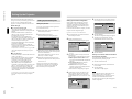
Plug the AC power cord into the wall outlet.
Press the I / 1 key to turn on the power.
Press the MENU key.
The menu display appears.
Press the M or m key to select the SET SETTING
menu, then press the , or ENTER key.
The SET SETTING menu appears.
INPUT-A
SET SETTING
STATUS:
ON
INPUT-A:
COMPUTER
AUTO INPUT SEL: OFF
LANGUAGE: ENGLISH
POWER SAVING: OFF
IR RECEIVER:
FRONT&REAR
VPL-PS10/PX10/PX15
.........................................................................................................................................................................................................
1) PowerPoint is a registered trademark of Microsoft Corporation (U.S.A. and other countries).
22 (GB)
23 (GB)
VPL-PS10/PX10/PX15
Projecting
Selecting the Menu Language / Projecting
5
6
Press the M or m key to select LANGUAGE, then
press the , or ENTER key.
Press the M or m key to select a language, then
press the < or ENTER key.
The menu changes to the selected language.
To clear the menu display
Press the MENU key.
The menu display disappears automatically if no key
is pressed for one minute.
1
2
3
ON/STANDBY
indicator
LAMP/
COVER
VOLUME
APA
TEMP/
FAN
3 2
POWER
ON/
SAVING STANDBY
HELP
MENU
RESET
ENTER
INPUT
Press the I / 1 key to turn on the projector.
The ON/STANDBY indicator lights in green.
Turn on all equipment connected to the projector.
Press the INPUT key to select the input source.
INPUT-A: Selects the video signal input from the
INPUT A connector.
INPUT-B (VPL-PX15 only): Selects display of
the INPUT B (Windows CE) window.
VIDEO: Selects the video signal input from the
VIDEO jack on the video input connectors.
S-VIDEO: Selects the video signal input from the
S VIDEO connector on the video input
connectors.
Projecting
APA key
After all equipment is connected completely, plug
the AC power cord into the wall outlet.
The ON/STANDBY indicator lights in red and the
projector goes into the standby mode.
4
Turn the zoom ring to adjust the size of the
picture.
5
Turn the focus ring to adjust the focus.
COMMAND
OFF ON
PIC
AUDIO
INPUT
D KEYSTONE
HELP
VOLUME
APA
FREEZE
MENU/
TAB
LASER
2
3
When the base edge is longer than the upper
edge as shown in the figure below:
D KEYSTONE
APA
MENU
ENTER
APA key
+
–
ENTER
R
CLICK
To get the clearest picture
You can get the best picture automatically when a
signal from the computer is input. Press the APA key.
The picture is automatically adjusted to project the
clearest picture possible.
RESET
To correct trapezoidal distortion
To cut off the picture
Press the PIC MUTING key on the Remote
Commander (VPL-PX15/PX10 only). To restore the
picture, press the PIC MUTING key again.
INPUT
For details on the INPUT SETTING menu, see page 29
(GB).
Looking into the lens when the projector is projecting
an image may cause injury to your eyes.
FREEZE MS SLIDE I / 1
PJ NETWORK MUTING
To turn off the power
When the projected image is a trapezoid, correct it by
pressing the D KEYSTONE key on the Remote
Commander or by adjusting DIGIT KEYSTONE in
the INSTALL SETTING menu.
Note
Rear remote
control detector
Notes
• Adjust the signal when a still picture is displayed on
the screen.
• Press the APA key when the full image is displayed
on the screen. If there are black edges around the
image, the APA function will not function properly
and the image may extend beyond the screen.
• If you switch the input signal or re-connect a
computer, press the APA key again to get the
suitable picture.
• “ADJUSTING” appears on the screen. To restore the
original screen, press the APA key again during the
adjustment.
• “Complete!” appears on the screen when the picture
is adjusted properly. However, depending on the
kinds of input signal, the picture may not always be
adjusted properly.
• Adjust the items in the INPUT SETTING menu
when you adjust the picture manually.
Set the value to negative.
When the upper edge is longer than the base
edge as shown in the figure below:
Set the value to positive.
1
Press the I / 1 key.
“Power OFF?” appears on the screen.
Note
The message will disappear if you press any key
except the I / 1 key, or if you do not press any
key for five seconds.
2
Press the I / 1 key again.
The ON/STANDBY indicator flashes in green and
the fan continues to run for about 90 seconds to
reduce internal heat build-up. Also, the ON/
STANDBY indicator flashes quickly for the first
60 seconds. During this first 60 seconds, you will
not be able to turn the power back on with the
I / 1 key.
3
Unplug the AC power cord from the wall outlet
after the fan stops running and the ON/STANDBY
indicator lights in red.
When you cannot confirm the on-screen
message
When you cannot confirm the on-screen message at
anytime, you can turn off the power by holding the
I / 1 key for about one second.
Note
Do not unplug the AC power cord while the
fan is still running; otherwise, the fan will
stop even though the internal heat level is
still high. This may lead to a breakdown of the
projector.
Cleaning the air filter
Clean the air filter every 300 hours to ensure
optimal performance.
For details on “DIGIT KEYSTONE,” see page 33 (GB).
R
CLICK
D ZOOM
1 FUNCTION
2
RESET/
ESCAPE
D ZOOM
1
2
3
FUNCTION
RM-PJM15
PROJECTOR
for VPL-PX15/PX10
24 (GB)
for VPL-PS10
25 (GB)
1-13
1-14
Projecting
Using the Menu
To freeze the image projected (Freeze
function)
Using the Menu
You can enlarge an area on the image you select.
This function works only when a signal from a
computer is input.
Press the FREEZE key. “FREEZE” appears when the
key is pressed. This function works only when a
signal from a computer is input.
To restore the original screen, press the FREEZE key
again.
The projector is equipped with an on-screen menu for
making various adjustments and settings.
1
Project the original size picture and press the D
ZOOM + key on the Remote Commander.
The Digital Zoom icon appears in the center of the
image.
Digital Zoom icon
To use the Laser Pointer function (VPLPX15/PX10 only)
Press the LASER key on the Remote Commander.
The laser pointer appears. The pointer is helpful in
indicating a particular point on the screen.
Note
(VPL-PX15/PX10 only)
Before operation, confirm that the PJ/NETWORK
select switch on the Remote Commander is set to PJ.
If it is set to NETWORK, the menu display will not
appear even when you press the MENU key on the
Remote Commander.
To select the language used in the menu, see page
23 (GB).
1
2
Move the icon to a point in the center of the
portion of the image you want to enlarge. Use the
arrow keys (M/m/</,) to move the icon.
3
Press the D ZOOM + key again.
The portion of the image where the icon is located
is enlarged. The magnification ratio is displayed
on the screen for a few seconds.
By pressing the + key repeatedly, the image size
increases (maximum magnification: 4 times) .
To clear the menu
Press the MENU key.
The menu display disappears automatically if no key
is pressed for one minute.
Press the MENU key.
The menu display appears.
The menu presently selected is shown as a yellow
button.
To reset items that have been adjusted
Press the RESET key.
“Complete!” appears on the screen and the settings
appearing on the screen will be reset to their factory
preset values.
Items that can be reset are:
• “CONTRAST, ” “BRIGHT, ” “COLOR, ” “HUE,”
“SHARP,” and “RGB ENHANCER” in the
PICTURE CTRL menu.
• “DOT PHASE, ” “SIZE H,” and “SHIFT” in the
INPUT SETTING menu.
• “DIGIT KEYSTONE” in the INSTALL SETTING
menu.
INPUT-A
PICTURE CTRL
CONTRAST:
80
BRIGHT:
50
About the retention of the settings
RGB ENHANCER: 30
GAMMA MODE: GRAPHICS
COLOR TEMP: LOW
VOLUME:
2
When no signal is input
Use the M or m key to select a menu, then press
the , or ENTER key.
The selected menu appears.
Menus
When there is no input signal, “NO INPUT–Cannot
adjust this item.” appears on the screen, and the items
mentioned above cannot be adjusted.
Setting items
INPUT-A
SET SETTING
Use the arrow keys (M/m/</,) to scroll the
enlarged image.
The settings are automatically stored in the projector
memory.
50
STATUS:
ON
INPUT-A:
COMPUTER
About the menu display
AUTO INPUT SEL: OFF
LANGUAGE: ENGLISH
POWER SAVING: OFF
IR RECEIVER:
FRONT&REAR
You can set the display position of the menu, the
intensity of the background picture, and the color of
the menu items as you like.
For details, see page 33 (GB).
To return the image to its original size
Press the D ZOOM – key. Pressing the RESET key
returns the image to its original size in one operation.
3
Select an item.
Use the M or m key to select the item, then press
the , or ENTER key.
4
Make settings or adjustments on an item.
For details on setting individual items, see the relevant
menu pages.
VPL-PS10/PX10/PX15
26 (GB)
27 (GB)
Adjustments and Settings Using the Menu
To enlarge the image (Digital Zoom
function)
VPL-PS10/PX10/PX15
The PICTURE CTRL Menu / The INPUT SETTING Menu
The PICTURE CTRL Menu
The PICTURE CTRL Menu
The PICTURE CTRL (control) menu is used for
adjusting the picture.
Unadjustable items for a particular input signal are not
displayed in the menu.
BRIGHT
Adjusts the picture brightness.
The higher the setting, the brighter the picture.
The lower the setting, the darker the picture.
COLOR
When the video signal is input
VIDEO
PICTURE CTRL
CONTRAST:
BRIGHT:
80
50
COLOR:
50
HUE:
50
SHARP:
50
D.PICTURE:
ON
HUE
Adjusts color tones.
The higher the setting, the more the picture becomes
greenish.
The lower the setting, the more the picture becomes
purplish.
COLOR TEMP: LOW
COLOR SYS: AUTO
VOLUME:
Adjusts color intensity.
The higher the setting, the greater the intensity.
The lower the setting, the lower the intensity.
50
COLOR SYS (System)
The INPUT SETTING Menu
Selects the color system of the input signal.
AUTO: Automatically selects one of the following
signals: NTSC3.58, PAL, SECAM, NTSC4.43.
PAL-M/N: Automatically selects one of the
following signals: PAL-M/PAL-N, NTSC3.58.
Normally, set to AUTO.
If the picture is distorted or colorless, select the color
system appropriate to the input signal.
The INPUT SETTING menu is used to adjust the
input signal.
Unadjustable items for a particular input signal are not
displayed in the menu.
INPUT-A
PICTURE CTRL
CONTRAST:
80
BRIGHT:
50
RGB ENHANCER: 30
GAMMA MODE: GRAPHICS
Adjusts the picture sharpness.
The higher the setting, the sharper the picture.
The lower the setting, the softer the picture.
COLOR TEMP: LOW
VOLUME:
RGB ENHANCER
Adjusts the picture sharpness when RGB signals are
input.
The higher the setting, the sharper the picture.
The lower the setting, the softer the picture.
Operation
1. Select an item
Use the M or m key to select the item, then press the
, or ENTER key.
2. Adjust an item
• When changing the adjustment level:
To increase the value, press the M or , key.
To decrease the value, press the m or < key.
Press the ENTER key to restore the original screen.
• When changing the setting:
Press the M or m key to change the setting.
Press the ENTER or < key to restore the original
screen.
CONTRAST
Adjusts the picture contrast.
The higher the setting, the greater the contrast.
The lower the setting, the lower the contrast.
28 (GB)
SHIFT
D. (Dynamic) PICTURE
Emphasizes the black color.
ON: Emphasizes the black color to produce a bolder
“dynamic” picture.
OFF: Reproduces the dark portions of the picture
accurately, in accordance with the source signal.
GAMMA MODE
Selects a gamma correction curve.
GRAPHICS: Improves the reproduction of half
tones. Photos can be reproduced in natural tones.
TEXT: Contrasts black and white. Suitable for
images that contain lots of text.
COLOR TEMP
Adjusts the color temperature.
HIGH: Makes the white color bluish.
LOW: Makes the white color reddish.
H: 200
V: 30
16:9
Memory No.
NO.01
VOLUME
VIDEO/60
Adjusts the volume. The volume can be adjusted for
each of INPUT A, INPUT B (VPL-PX15 only),
VIDEO and S VIDEO input.
Input signals and adjustable/setting items
Item
When the RGB signal is input
INPUT-A
INPUT SETTING
Input signal
Video or
S video (Y/C)
Signal type
Component Video GBR
RGB1)
DOT PHASE:
0
SIZE H:
1056
SHIFT
H: 200
V: 30
SCAN CONV: ON
CONTRAST
BRIGHT
50
VIDEO
INPUT SETTING
ASPECT:
When the RGB signal is input
SHARP
When the video signal is input
NO.17
COLOR
Memory No.
800x600
–
(except for B & W)
HUE
Signal type
–
(NTSC3.58/
4.43 only)
SHARP
RGB
ENHANCER
–
–
–
D. PICTURE
GAMMA
MODE
–
–
–
Operation
–
1. Select an item
Use the M or m key to select the item, then press the
, or ENTER key.
–
2. Adjust an item
• When changing the adjustment level:
To increase the value, press the M or , key.
To decrease the value, press the m or < key.
Press the ENTER key to restore the original screen.
–
–
COLOR
TEMP
COLOR
SYS
–
VOLUME
: Adjustable/can be set
– : Not adjustable/can not be set
1) The RGB signals of a computer
–
• When changing the setting:
Press the M or m key to change the setting.
Press the ENTER or < key to restore the original
screen.
DOT PHASE
Adjusts the dot phase of the LCD panel and the signal
input from the INPUT A/B connector. Adjust the
picture further for a finer picture after the picture is
adjusted by pressing the APA key. Adjust the picture
to the point where it looks clearest.
29 (GB)
1-15
1-16
The INPUT SETTING Menu
SIZE H
Adjusts the horizontal size of the picture input from
the INPUT A/B connector.
The higher the setting, the larger the horizontal size of
the picture.
The lower the setting, the smaller the horizontal size
of the picture. Adjust the setting according to the dots
of the input signal.
For details on a suitable value for preset signals, see page
31 (GB).
SHIFT
Adjusts the position of the picture input from the
INPUT A/B connectors or video input connectors.
H adjusts the horizontal position of the picture.
V adjusts the vertical position of the picture.
As the setting for H increases, the picture moves to
the right, and as the setting decreases, the picture
moves to the left.
As the setting for V increases, the picture moves up,
and as the setting decreases, the picture moves down.
Use the < or , key to adjust the horizontal position
and the M or m key for the vertical position.
ASPECT
Sets the aspect ratio of the picture.
When inputting a 16:9 (squeezed) signal from
equipment such as a DVD player, set this to 16:9.
4:3 : When a picture with a ratio of 4:3 is input.
16:9 : When a picture with a ratio of 16:9 (squeezed)
is input.
SCAN CONV (Scan converter)
Converts the signal to display the picture according to
the screen size.
ON: Displays the picture according to the screen
size. The picture will lose some clarity.
OFF: Displays the picture while matching one pixel
of the input picture element to that of the LCD.
The picture will be clear but the picture size will
be smaller.
Note
VPL-PS10/PX10/PX15
This item will not be displayed in the following cases.
VPL-PX15/PX10: When an XGA or SXGA signal is
input.
VPL-PS10: When an SVGA, XGA or SXGA signal is
input.
30 (GB)
The INPUT SETTING Menu / The SET SETTING Menu
Input signals and adjustable/setting items
Item
Input signal
Video or
S video (Y/C)
Component
DOT
PHASE
–
–
SIZE H
–
–
Video GBR
RGB1)
–
–
SHIFT
ASPECT
SCAN
CONV
–
–
–
–
2)
: Adjustable/can be set
– : Not adjustable/can not be set
1) The RGB signals of a computer
2) VPL-PX15/PX10: lower than SVGA only; VPL-PS10:
lower than VGA only
About the preset memory No.
This projector has 37 kinds of preset data for input
signals (the preset memory). The memory number of
the current input signal and the signal type are
displayed when the preset signal is input. This
projector automatically detects the signal type. When
the signal has been registered in the preset memory, a
suitable picture is displayed on the screen according to
the signal type. You can adjust the picture through the
INPUT SETTING menu.
This projector also has 20 kinds of user memories for
each INPUT A/B. When an unpreset signal is input
for the first time, the memory number is displayed as
0. If the input signal is adjusted in the INPUT
SETTING menu, the setting made via INPUT A/B is
stored. When more than 20 user memory items are
registered for each INPUT A/B, the newest memory
item is automatically stored over the oldest one.
Preset signals
Memory Preset signal
No.
fH
fV
(kHz) (Hz)
Sync
1
2
3
4
6
7
8
9
10
11
12
13
14
15
16
17
18
19
20
21
22
23
24
25
26
27
28
29
30
31
32
33
34
35
36
37
38
15.734
15.625
15.734
15.625
31.469
37.861
24.823
31.469
37.861
31.469
35.000
37.861
37.500
43.269
35.156
37.879
48.077
46.875
53.674
49.724
35.524
48.363
56.476
60.023
68.677
63.995
67.500
77.487
61.795
71.713
60.000
75.000
46.433
53.316
63.974
79.976
91.146
H-neg V-neg
H-neg V-neg
Video 60 Hz
Video 50 Hz
480/60i
575/50i
640 × 350 VGA mode 1
VGA VESA1) 85 Hz
640 × 400 PC-98012) Normal
VGA mode 2
VGA VESA 85 Hz
640 × 480 VGA mode 3
Macintosh 13”
VGA VESA 72 Hz
VGA VESA 75 Hz
VGA VESA 85 Hz
800 × 600 SVGA VESA 56 Hz
SVGA VESA 60 Hz
SVGA VESA 72 Hz
SVGA VESA 75 Hz
SVGA VESA 85 Hz
832 × 624 Macintosh 16”
1024 × 768 XGA VESA 43 Hz
XGA VESA 60 Hz
XGA VESA 70 Hz
XGA VESA 75 Hz
XGA VESA 85 Hz
1152 × 864 SXGA VESA 70 Hz
SXGA VESA 75 Hz
SXGA VESA 85 Hz
1152 × 900 Sunmicro LO
Sunmicro HI
1280 × 960 SXGA VESA 60 Hz
SXGA VESA 75 Hz
1280 × 1024 SXGA VESA 43 Hz
SGI-5
SXGA VESA 60 Hz
SXGA VESA 75 Hz
SXGA VESA 85 Hz
59.940
50.000
59.940
50.000
70.086
85.080
56.416
70.086
85.080
59.940
66.667
72.809
75.000
85.008
56.250
60.317
72.188
75.000
85.061
74.550
43.479
60.004
69.955
75.029
84.997
70.016
75.000
85.057
65.960
76.047
60.000
75.000
43.436
50.062
60.013
75.025
85.024
SIZE
H
S on G/Y or
Composite sync
H-pos V-neg
H-pos V-neg
H-neg V-neg
H-neg V-pos
H-neg V-pos
H-neg V-neg
H-neg V-neg
H-neg V-neg
H-neg V-neg
H-neg V-neg
H-pos V-pos
H-pos V-pos
H-pos V-pos
H-pos V-pos
H-pos V-pos
H-neg V-neg
H-pos V-pos
H-neg V-neg
H-neg V-neg
H-pos V-pos
H-pos V-pos
H-pos V-pos
H-pos V-pos
H-pos V-pos
H-neg V-neg
Composite sync
H-pos V-pos
H-pos V-pos
H-pos V-pos
S on G
H-pos V-pos
H-pos V-pos
H-pos V-pos
800
832
848
800
832
800
864
832
840
832
1024
1056
1040
1056
1048
1152
1264
1344
1328
1312
1376
1472
1600
1568
1504
1472
1800
1728
1696
1680
1696
1688
3)
1) VESA is a registered trademark of the Video Electronics
Standards Association.
2) PC-98 is a registered trademark of NEC Corporation.
3) VPL-PX15/PX10: 1296; VPL-PS10: 1012.
Since the data is recalled from the preset memory for
the following signals, you can use this preset data by
adjusting SIZE H. Make finer adjustments using
SHIFT.
Signal
Memory No.
SIZE H
Super Mac-2
23
1312
SGI-1
23
1320
Macintosh 19”
Macintosh 21”
25
1328
27
1456
Sony News
36
1708
PC-9821
1280 × 1024
36
1600
WS Sunmicro
37
1664
Note
When the aspect ratio of an input signal is other than
4:3, a part of the screen is displayed in black.
The SET SETTING Menu
The SET SETTING menu is used for changing the
settings of the projector.
INPUT-A
SET SETTING
STATUS:
ON
INPUT-A:
COMPUTER
AUTO INPUT SEL: OFF
LANGUAGE: ENGLISH
POWER SAVING: OFF
IR RECEIVER:
FRONT&REAR
Operation
1. Select an item
Use the M or m key to select the item, then press the
, or ENTER key.
2. Change the setting
Press the M or m key to change the setting.
To restore the original screen, press the ENTER or <
key.
31 (GB)
VPL-PS10/PX10/PX15
The INSTALL SETTING Menu
The SET SETTING Menu / The INSTALL SETTING Menu
STATUS (on-screen display)
Sets up the on-screen display.
ON: Shows all of the on-screen display.
OFF: Turns off the on-screen display except for the
menus, a message when turning off the power,
and warning messages.
The INSTALL SETTING
Menu
The INSTALL SETTING menu is used for changing
the install settings of the projector.
For details on the warning messages, see page 40 (GB).
KEYSTONE MEM: ON
Selects the computer, component or video GBR (15k
RGB) signal input from the INPUT A connector.
MENU POSITION: CENTER
DIGIT KEYSTONE: 0
MENU COLOR:
STANDARD
MENU BACKGRND:
STANDARD
INPUT-B FUNC.:
ON
LAMP TIMER: 234H
AUTO INPUT SEL
When set to ON, the projector detects input signals in
the following order: INPUT-A/INPUT-B (VPL-PX15
only)/VIDEO/S-VIDEO. It indicates the input channel
when the power is turned on or the INPUT key is
pressed.
LANGUAGE
Selects the language used in the menu and on-screen
displays.
Available languages are: English, French, German,
Italian, Spanish, Japanese, Chinese, Portuguese and
Korean.
POWER SAVING
When set to ON, the projector goes into the power
saving mode if no signal is input for 10 minutes.
IR RECEIVER
Selects the remote control detectors on the front and
rear of the projector.
FRONT & REAR: Activates both the front and rear
detectors.
FRONT: Activates the front detector only.
REAR: Activates the rear detector only.
32 (GB)
INPUT-B FUNC. (VPL-PX15 only)
Set to ON when using the Windows CE function.
Note
Be sure to exit every application that is open before
you switch the setting from ON to OFF. Otherwise,
the system may crash and you may not be able to
restart the projector.
DIGIT KEYSTONE
LAMP TIMER
CEILING-FRONT
Note
If the setting is not correct, “Please check INPUT-A
setting.” appears on the screen and the color of the
picture becomes strange or the picture is not
displayed.
ON: The DIGIT KEYSTONE setting is stored.
The data is retrieved when the projector power is
turned on. The setting will remain the same every
time.
OFF: The DIGIT KEYSTONE is reset to 0 when the
power is turned on next time.
INPUT-A
INSTALL SETTING
INPUT-A
INSTALLATION:
KEYSTONE MEM
Corrects the trapezoidal distortion caused by the
projection angle.
If the base edge of the image is longer, set a negative
value; if the upper edge is longer, set a positive value
to display the image as a rectangle.
Indicates how long the lamp has been turned on.
Note
This only displays the time. You cannot alter the
display.
INSTALLATION
INPUT-B FUNC. is displayed only for the VPLPX15.
Operation
1. Select an item
Use the M or m key to select the item, then press the
, or ENTER key.
2. Adjust an item
• When changing the adjustment level:
To increase the value, press the M or , key.
To decrease the value, press the m or < key.
Press the ENTER key to restore the original screen.
• When changing the setting:
Press the M or m key to change the setting.
Press the ENTER or < key to restore the original
screen.
Set this item to reverse the picture horizontally or
vertically.
FLOOR-FRONT: The picture is not reversed.
CEILING-FRONT: The picture is reversed
horizontally and vertically.
FLOOR-REAR: The picture is reversed
horizontally.
CEILING-REAR: The picture is reversed
vertically.
Note
When using a mirror, be careful of how the
installation is carried out since the picture may be
reversed.
MENU POSITION
Selects the display position of the menu from TOP
LEFT, BOTTOM LEFT, CENTER, TOP RIGHT and
BOTTOM RIGHT.
MENU COLOR
Selects the tone of the menu display from
STANDARD, WARM, COOL, GREEN or GRAY.
MENU BACKGRND
Selects the intensity of the background picture of the
menu display from DARK, STANDARD or LIGHT.
33 (GB)
1-17
Distance between the front of the
cabinet and the center of the lens
a: Distance between the screen and the center
of the lens
b: Distance from the floor to the center of the
lens
c: Distance from the floor to the foot of the
projector
x: Free
Standard lens:
–25.4
– mm (–1 inch)
+ 0
Very dusty
Unsuitable Installation
Do not install the projector in the following situations.
These installations may cause malfunction or damage
to the projector.
PUSH
Wall
Notes for Installation
Poorly ventilated
Avoid installing the unit in a location where there is a
lot of dust; otherwise, the air filter will clog. The dust
blocking the air through the filter may cause the
internal heat level of the projector to rise. Clean the
filter periodically.
Center of the screen
Unsuitable Conditions for Use
PUSH
x
Center of the lens
c
b
Do not do any of the following.
Floor
Toppling the unit
a
VPL-PX15/PX10
SS
Unit: mm (inches)
40
60
80
100
120
150
180
200
250
300
Minimum
1458
(57 1/2)
2217
(87 1/2)
2977
(117 3/8)
3736
(147 3/8)
4495
(177 1/4)
5635
(221 3/4)
6774
(266 5/8)
7533
(296 1/2)
9432
(371 3/8)
11330
(446 1/8)
Maximum
1764
(69 3/8)
2675
(105 1/4)
3586
(141 3/8)
4497
(177 1/4)
5408
(213 1/8)
6774
(266 5/8)
8141
(320 5/8)
9052
(356 3/8)
11329
(446 1/8)
13607
(536)
b
x–305
(12)
x–457
(18)
x–610
(24)
x–762
(30)
x–914
(36)
x–1143
(45)
x–1372
(54)
x–1524
(60)
x–1905
(75 1/8)
x–2286
(90 1/8)
c
x–388
(15 3/8)
x–541
(21 3/8)
x–693
(27 3/8)
x–845
(33 3/8)
x–998
(39 3/8)
x–1226
(48 3/8)
x–1455
(57 3/8)
x–1607
(63 3/8)
x–1988
(78 3/8)
x–2369
(93 3/8)
a
• Allow adequate air circulation to prevent internal
heat build-up. Do not place the unit on surfaces
(rugs, blankets, etc.) or near materials (curtains,
draperies) that may block the ventilation holes.
When internal heat builds up due to blockage of the
ventilation holes, the temperature sensor may
function, a warning message will be displayed, and
the power may be turned off automatically after one
minute.
• Leave space of more than 50 cm (19 3/4 inches)
around the unit.
• Be careful that the ventilation holes do not inhale
tiny objects such as pieces of paper.
Avoid standing the unit on its side as the unit may
topple over. This may cause a malfunction.
Tilting the unit more than 15 degrees
To calculate the installation measurements (unit: mm)
SS: screen size diagonal (inches)
a (minimum) = {(SS × 33.60/0.9071) – 59.7012} × 1.025
a (maximum) = {(SS × 42.376846/0.9071) – 59.62151} × 0.975
b = x – (SS/0.9071 × 6.912)
c = x – (SS/0.9071 × 6.912 + 83.4)
Highly heated and humid
VPL-PS10
Unit: mm (inches)
40
60
80
100
120
150
180
200
250
300
Minimum
1461
(57 1/2)
2221
(87 1/2)
2982
(117 3/8)
3742
(147 3/8)
4503
(177 1/4)
5644
(222 1/8)
6784
(267)
7545
(297 3/8)
9446
(372 1/8)
11348
(447)
Maximum
1767
(69 3/4)
2680
(105 5/8)
3592
(141 3/8)
4505
(177 1/4)
5417
(213 1/2)
6786
(267 3/8)
8154
(321)
9067
(357 1/4)
11348
(447)
13629
(536 3/4)
b
x–305
(12 1/8)
x–458
(18 1/8)
x–611
(24 1/8)
x–763
(30 1/8)
x–916
(36 1/8)
x–1145
(45 1/8)
x–1374
(54 1/8)
x–1527
(60 1/8)
x–1908
(75 1/4)
x–2290
(90 1/4)
c
x–389
(15 3/8)
x–541
(21 3/8)
x–694
(27 3/8)
x–847
(33 3/8)
x–999
(39 3/8)
x–1228
(48 3/8)
x–1457
(57 3/8)
x–1610
(63 1/2)
x–1992
(78 1/2)
x–2373
(93 1/2)
a
PUSH
SS
• Avoid installing the unit in a location where the
temperature or humidity is very high, or the
temperature is very low.
• To avoid moisture condensation, do not install the
unit in a location where the temperature may rise
rapidly.
Avoid tilting the unit at an angle of more than 15
degrees. Installation of the unit in this manner may
cause a malfunction.
To calculate the installation measurements (unit: mm)
VPL-PS10/PX10/PX15
SS: screen size diagonal (inches)
a (minimum) = {(SS × 33.59/0.9055) –59} × 1.025
a (maximum) = {(SS × 42.370377/0.9055) – 58.9761} × 0.975
b = x – (SS/0.9055 × 6.912)
c = x – (SS/0.9055 × 6.912 + 83.4)
34 (GB)
35 (GB)
Installation
Installation Example
PUSH
1-18
Notes for Installation
Installation Example
Blocking the ventilation holes
Maintenance
Maintenance
3
Loosen the screws on the lamp unit with the
Phillips screwdriver.
4
While holding the handle and keeping the lamp
unit horizontal, pull straight up.
5
Insert the new lamp all the way in until it is
securely in place. Tighten the two screws. Fold
down the handle.
Notes
Avoid using something that covers over the
ventilation holes (exhaust/intake); otherwise, the
internal heat level may build up.
Removing the adjusters
• If the lamp breaks, consult with qualified Sony
personnel.
• Pull out the lamp unit by holding the handle. If you
touch the lamp unit, you may be burned or injured.
• When removing the lamp unit, make sure it remains
horizontal, then pull straight up. Do not tilt the lamp
unit. If you pull out the lamp unit while it is tilted
and if the lamp breaks, the pieces may scatter,
causing injury.
Replacing the Lamp
Avoid using the unit with the adjusters removed.
Blocking the ventilation holes (intake) may cause
internal heat build-up.
When the lamp has burnt out or dims, or “Please
replace the LAMP.” appears on the screen, replace the
lamp with a new one. The lamp life varies depending
on conditions of use. The message appears after 1500
hours of use.
Use an LMP-P202 Projector Lamp as the replacement
lamp.
When replacing the lamp after using the
projector
Turn off the projector, then unplug the power cord.
Wait for at least an hour for the lamp to cool.
Note
The lamp remains at a high temperature after you turn
off the projector with the I / 1 key. If you touch the
lamp, you may burn your finger. When you replace
the lamp, wait for at least an hour for the lamp to cool.
1
Notes
Place a protective sheet (cloth) beneath the
projector. Hold the projector handle and place the
projector face down.
• Be careful not to touch the glass surface of the
lamp.
• The power will not turn on if the lamp is not
secured properly.
Note
When replacing the lamp, be sure the projector is
on a flat and stable surface.
2
Slide open the lamp cover after loosening its
screw with a Phillips screwdriver.
6
7
8
9
36 (GB)
Close the lamp cover and tighten the screw.
Turn the projector back over.
Connect the power cord and turn the projector to
the standby mode.
Press the following keys on the control panel in
the following order for less than five seconds
each: RESET, <, ,, ENTER.
37 (GB)
Maintenance
VPL-PS10/PX10/PX15
Notes for Installation
1-19
1-20
Troubleshooting
Maintenance
Notes
• Be sure to use an LMP-P202 Projector Lamp for
replacement. If you use lamps other than the LMPP202, the projector may malfunction.
• Be sure to turn off the projector and unplug the
power cord before replacing the lamp.
• Do not put your hands into the lamp replacement
socket, and do not allow any liquid or objects to fall
into it to avoid electrical shock or fire.
Disposal of a used projector lamp
As the materials used in this lamp are similar to those
of a fluorescent lamp, you should dispose of a used
projector lamp in the same way as a fluorescent lamp.
Cleaning the Air Filter
The air filter should be cleaned every 300 hours.
When it becomes difficult to remove the dust from the
filter, replace the filter with a new one.
To clean the air filter, follow the steps below:
1
2
5
Hook the air filter on the holders of the air filter
cover, then set the filter and replace the cover.
Notes
• If the dust cannot be removed from the air filter,
replace the air filter with the supplied new one.
• Be sure to attach the air filter cover firmly; the power
cannot be turned on if it is not closed securely.
• Place the air filter so that it fits in a notch on the air
filter cover.
To clean the ventilation holes
When you clean the air filter, clean the ventilation
holes (intake, rear and bottom) also. Remove the dust
from the outside of the ventilation holes with a
vacuum cleaner.
Troubleshooting
If the projector appears to be operating erratically, try to diagnose and correct the problem, using the following
guide. If the problem still persists, consult with qualified Sony personnel.
Power
Cause
The power is not turned on.
The power has been turned off and on
Wait for about 90 seconds before turning on the
with the I / 1 key at too short an interval. power (see page 25 (GB)).
Close the lamp cover securely (see page 37 (GB)).
The lamp cover is detached.
The air filter cover is detached.
Close the air filter cover securely (see page 38 (GB)).
Symptom
Cause
Remedy
No picture.
A cable is disconnected or not connected Check that the proper connections have been
properly.
made (see pages 18 (GB) to 23 (GB)).
The input selection is incorrect.
Select the input source correctly using the INPUT
key (see page 24 (GB)).
Image
The picture is cut off.
Press the PIC MUTING key on the VPL-PX15/
PX10 Remote Commander to release the muting
function (see page 14 (GB)).
The computer signal is not set to output
to an external monitor.
Set the computer signal to output to an external
monitor (see page 18 (GB)).
The computer signal is set to output to
both the LCD of the computer and an
external monitor.
Noise may appear on the background
depending on the combination of the
numbers of dot input from the connector
and numbers of pixels on the LCD panel.
Set the computer signal to output only to an
external monitor (see page 18 (GB)).
STATUS in the SET SETTING menu has
been set to OFF.
There is something wrong with the
Windows CE software.
Set STATUS in the SET SETTING menu to ON
(see page 32 (GB)).
Set INPUT-B FUNC. in the INSTALL SETTING
menu to OFF, then set it to ON again (see page
33 (GB)).
Set COLOR SYS in the PICTURE CTRL menu to
match the color system of the input signal (see
page 29 (GB)).
Turn off the power and unplug the power cord.
Remove the air filter cover at the bottom of the
projector.
The picture is noisy.
On-screen display does not
appear.
3
Remedy
Symptom
The picture from INPUT B is
frozen. (VPL-PX15 only)
Remove the air filter.
The color balance of the video The color system of the input signal is
not set correctly.
picture is not correct.
Change the desktop pattern on the connected
computer.
Sound
Cause
No Sound.
A cable is disconnected or not connected Check that the proper connections have been
properly.
made (see pages 18 (GB) to 23 (GB)).
The sound is cut off.
4
Wash the air filter with a mild detergent solution
and dry it in a shaded place.
VPL-PS10/PX10/PX15
38 (GB)
Remedy
Symptom
When inputting sound through Monaural sound is being input through
the AUDIO jack, sound comes the AUDIO jack.
through one channel only.
Press the AUDIO MUTING key on the VPL-PX15/
PX10 Remote Commander to release the muting
function (see page 14 (GB)).
Input stereo sound.
39 (GB)
Others
Remedy
Attach the cover securely (see pages 37 (GB) and
38 (GB)).
Replace the lamp (see page 37 (GB)).
Symptom
The LAMP/COVER indicator
flashes.
Cause
The lamp cover or the air filter cover is
detached.
The LAMP/COVER indicator
lights up.
The lamp has reached the end of its life.
The lamp has reached too a high
temperature.
Wait for 90 seconds to cool down the lamp and
turn on the power again (see page 25 (GB)).
The TEMP/FAN indicator
flashes.
The fan is broken.
Consult with qualified Sony personnel.
The TEMP/FAN indicator
lights up.
The internal temperature is unusually
high.
Check to see if nothing is blocking the ventilation
holes.
The electrical system has failed.
Both LAMP/COVER and
TEMP/FAN indicators light up.
Consult with qualified Sony personnel.
The INPUT B window does
not appear, or INPUT B
cannot be selected. (VPLPX15 only)
INPUT-B FUNC. is set to OFF.
Set INPUT-B FUNC. in the INSTALL SETTING
menu to ON (see page 33 (GB)).
The menu display does not
appear even when you press
the MENU key on the VPLPX15/PX10 Remote
Commander.
The PJ/NETWORK select switch on the
Remote Commander is set to
NETWORK.
Set the PJ/NETWORK select switch to PJ, then
press the MENU key.
Warning messages
Use the list below to check the meaning of the messages displayed on the screen.
Message
Meaning
Remedy
High temp.!
Lamp off in 1 min.
Internal temperature is too high.
Turn off the power.
Check to see if something is blocking the
ventilation holes.
Frequency is out of range!
This input signal cannot be projected as
the frequency is out of the acceptable
range of the projector.
Input a signal that is within the frequency range.
The resolution setting of the output
signal of the computer is too high.
Set the setting of output to XGA (VPL-PX15/PX10)
or SVGA (VPL-PS10) (see page 18 (GB)).
Set INPUT-A correctly (see page 32 (GB)).
Please replace the LAMP.
You have input an RGB signal from the
computer when INPUT-A in the SET
SETTING menu is set to COMPONENT
or VIDEO GBR.
It is time to replace the lamp.
Backup Battery Very Low
(VPL-PX15 only)
The backup battery for the Windows CE
OS is exhausted.
Consult with qualified Sony personnel.
Please check INPUT-A
setting.
80-inch: 2982 to 3592 mm
(117 3/8 to 141 3/8 inches)
100-inch: 3742 to 4505 mm
(147 3/8 to 177 1/4 inches)
120-inch: 4503 to 5417 mm
(177 1/4 to 213 1/2 inches)
150-inch: 5644 to 6786 mm
(222 1/8 to 267 3/8 inches)
180-inch: 6784 to 8154 mm
(267 to 321 inches)
200-inch: 7545 to 9067 mm
(297 3/8 to 357 1/4 inches)
250-inch: 9446 to 11348 mm
(372 1/8 to 447 inches)
300-inch: 11348 to 13629 mm
(447 to 536 3/4 inches)
Specifications
Replace the lamp.
Caution messages
Use the list below to check the meaning of the messages displayed on the screen.
Message
Meaning
Remedy
NO INPUT
No input signal
Check connections (see pages 18 (GB) to 23 (GB)).
Not applicable!
You have pressed the wrong key.
Press the appropriate key.
Optical characteristics
Projection system 3 LCD panels, 1 lens, projection
system
LCD panel
VPL-PX15/PX10: 0.9-inch TFT
LCD panel with micro-lens
array, 2,359,296 pixels
(786,432 pixels × 3)
VPL-PS10: 0.9-inch TFT LCD
panel, 1,440,000 pixels
(480,000 pixels × 3)
Lens
1.3 times zoom lens (manual)
f 33.6 to 42 mm/F 1.7 to 2.1
Lamp
200 W UHP
Projection picture size
Range: 40 to 300 inches (diagonal
measure)
Light output
VPL-PX15/PX10: ANSI lumen1)
2000 lm
VPL-PS10: ANSI lumen 1500 lm
Throwing distance VPL-PX15/PX10 (When an XGA
signal is input)
40-inch: 1458 to 1764 mm
(57 1/2 to 69 3/8 inches)
60-inch: 2217 to 2675 mm
(87 1/2 to 105 1/4 inches)
80-inch: 2977 to 3586 mm
(117 3/8 to 141 3/8 inches)
100-inch: 3736 to 4497 mm
(147 3/8 to 177 1/4 inches)
120-inch: 4495 to 5408 mm
(177 1/4 to 213 1/8 inches)
150-inch: 5635 to 6774 mm
(221 3/4 to 266 5/8 inches)
180-inch: 6774 to 8141 mm
(266 5/8 to 320 5/8 inches)
200-inch: 7533 to 9052 mm
(296 1/2 to 356 3/8 inches)
250-inch: 9432 to 11329 mm
(371 3/8 to 446 1/8 inches)
300-inch: 11330 to 13607 mm
(446 1/8 to 536 inches)
VPL-PS10 (When an SVGA signal
is input)
40-inch: 1461 to 1767 mm
(57 1/2 to 69 3/4 inches)
60-inch: 2221 to 2680 mm
(87 1/2 to 105 5/8 inches)
Electrical characteristics
Color system
NTSC3.58/PAL/SECAM/NTSC4.43/
PAL-M/PAL-N system,
switched automatically/manually
Resolution
VPL-PX15/PX10: 750 horizontal
TV lines (Video input) 1024 ×
768 dots (RGB input)
VPL-PS10: 600 horizontal TV
lines (Video input) 800 × 600
dots (RGB input)
Acceptable computer signals
fH: 15 to 91 kHz
fV: 43 to 85 Hz
Speaker
Stereo speakers system, 28 mm
(1 1/8 inches) diameter,
max. 0.5 W × 2
Input/Output
Video input
S VIDEO: Y/C mini DIN 4-pin
type (female)
Y (luminance): 1 Vp-p ±2 dB
sync negative (75 ohms
terminated)
C (chrominance): burst
0.286 Vp-p ±2 dB (NTSC)
(75 ohms terminated),
burst 0.3 Vp-p ±2 dB (PAL)
(75 ohms terminated)
VIDEO: phono type
Composite video: 1 Vp-p ±2 dB
sync negative (75 ohms
terminated)
.........................................................................................................................................................................................................
1) ANSI lumen is a measuring method of American National Standards Institute IT7.228.
40 (GB)
41 (GB)
Other
VPL-PS10/PX10/PX15
Specifications
Troubleshooting
1-21
1-22
Specifications
Specifications
AUDIO: Stereo minijack 500
mVrms, impedance more than 47
kilohms
INPUT A
INPUT A: HD D-sub 15-pin
(female)
Analog RGB/component:
R/R-Y: 0.7 Vp-p ±2 dB
(75 ohms terminated)
G: 0.7 Vp-p ±2 dB
(75 ohms terminated)
G with sync/Y: 1 Vp-p ±2 dB
sync negative
(75 ohms terminated)
B/B-Y: 0.7 Vp-p ±2 dB
(75 ohms terminated)
SYNC/HD: Composite sync
input: 1-5 Vp-p high impedance,
positive/negative
Horizontal sync input: 1-5 Vp-p
high impedance, positive/
negative
VD: Vertical sync input: 1-5
Vp-p high impedance, positive/
negative
AUDIO: Stereo minijack
500 mVrms, impedance more
than 47 kilohms
MOUSE
6-pin (female) (For details, see
“Pin assignment” on page 43
(GB).)
INPUT B (VPL-PX15 only)
ETHER
10BASE-T standard
100BASE-TX standard
PC CARD slot
PC CARD slot Type II
USB hub
Up (B type: female) × 1
Down (A type: female) × 1
CONTROL S IN/PLUG IN POWER
Stereo minijack 5 Vp-p, plug in
power, 5 V DC
Safety regulations
UL1950
cUL (CSA No. 950)
FCC Class A
IC Class A
NEMKO (EN60950)
CE (LVD, EMC)
C-Tick
VPL-PS10/PX10/PX15
42 (GB)
Laser beam (VPL-PX15/PX10 only)
Laser type
Wavelength
Output
Class 2
645 nm
1 mW
General
325 × 110 × 285 mm (12 7/8 × 4 3/8
× 11 1/4 inches) (w/h/d)
(without the projection parts)
Mass
VPL-PX15: Approx. 5.3 kg
(11 lb 11 oz)
VPL-PX10/PS10: Approx. 4.9 kg
(10 lb 13 oz)
Power requirements
VPL-PX15:
AC 100 to 240 V, 3.0–1.25 A,
50/60 Hz
VPL-PX10/PS10:
AC 100 to 240 V, 2.9–1.2 A,
50/60 Hz
Power consumption
VPL-PX15: Max. 300 W
(Standby mode: 4.9 W)
(When INPUT-B FUNC. is set to
ON: 9.0 W)
VPL-PX10/PS10: Max. 290 W
(Standby mode: 4.7 W)
Heat dissipation VPL-PX15: 1023.9 BTU
VPL-PX10/PS10: 989.6 BTU
Operating temperature
0 °C to 35 °C (32 °F to 95 °F)
Operating humidity
35 % to 85 % (no condensation)
Storage temperature
–20 °C to 60 °C (–4 °F to 140 °F)
Storage humidity 10 % to 90 %
Supplied accessories
Remote Commander RM-PJM15
(VPL-PX15/PX10 only) (1)
Remote Commander RM-PJM11
(VPL-PS10 only) (1)
R6 (Size AA) batteries (2)
HD D-sub 15-pin cable (2 m) (1)
(1-791-992-21)
PS/2 Mouse Cable (2 m) (1)
(1-792-424-12)
USB cable A type – B type (1)
(1-790-081-11)
CD-ROM (Application software)
(1)
Strap for Remote Commander
(VPL-PX15/PX10 only) (1)
Dimensions
AC power cord (1)
Air filter (for replacement) (1)
Lens cap (1)
Operating Instructions (1)
Operating Instructions for
Networking (VPL-PX15 only) (1)
Installation Manual for Dealers (1)
Specified/recommended PC Card/
Wireless LAN Access Point
(VPL-PX15 only) (1)
Quick Reference Card (1)
Design and specifications are subject to change
without notice.
Optional accessories
Projector Lamp LMP-P202 (for replacement)
Projector Suspension Support PSS-610
Monitor Cable
SMF-410 (HD D-sub 15-pin (male) y HD D-sub
15-pin (male))
Signal Cable
SMF-402 (HD D-sub 15-pin (male) y 3 × phono
jack)
Signal Adapter
ADP-20 (Macintosh y HD D-sub 15-pin)
Projection Lens
Short Focal Length Converter Lens VPLL-CW10
Long Focal Length Converter Lens VPLL-CT10
Some of the items may not be available in some areas. For
details, please consult your nearest Sony dealer.
Pin assignment
INPUT A connector (HD D-sub 15-pin, female)
1
R/R-Y
9
N.C.
2
G/Y
10
GND
3
B/B-Y
11
GND
4
GND
12
DDC/SDA
HD/C.Sync
5
GND
13
6
GND (R)
14
VD
7
GND (G)
15
DDC/SCL
8
GND (B)
MOUSE connector (6-pin, female)
6 5 4
3 2 1
1
DATA
2
N.C.
3
GND
4
+5 V
5
CLK
6
N.C.
43 (GB)
VPL-PS10/PX10/PX15
Index
Index
A
Adjuster 11 (GB)
Adjusting
retention of the settings 27 (GB)
the picture 28 (GB)
the picture size/shift 24 (GB)
Air filter 38 (GB)
APA function 24 (GB)
ASPECT 30 (GB)
AUTO INPUT SEL 32 (GB)
B
Battery
installation 16 (GB), 17 (GB)
notes 16 (GB), 17 (GB)
BRIGHT 28 (GB)
C
Carrying handle 9 (GB)
COLOR 28 (GB)
COLOR SYS (System) 29 (GB)
COLOR TEMP 28 (GB)
Condensation 35 (GB)
Connections
component equipment 20 (GB)
computer 18 (GB)
LAN 21 (GB)
VCR 20 (GB)
CONTRAST 28 (GB)
Cut off
the picture 24 (GB)
the sound 14 (GB)
D, E, F
DIGIT KEYSTONE 33 (GB)
D. (Dynamic) PICTURE 28 (GB)
DOT PHASE 29 (GB)
Freeze function 26 (GB)
G
GAMMA MODE 28 (GB)
H
HUE 28 (GB)
44 (GB)
I, J, K
R
INPUT-A 32 (GB)
INPUT-B FUNC. 33 (GB)
INPUT SETTING menu 29 (GB)
INSTALL SETTING menu 32 (GB)
INSTALLATION 33 (GB)
Installation example 34 (GB)
IR RECEIVER 32 (GB)
KEYSTONE MEM 33 (GB)
Remote Commander (VPL-PS10)
16 (GB)
Remote Commander (VPL-PX15/PX10)
14 (GB)
Remote control detector
front 9 (GB)
rear 9 (GB)
setting 32 (GB)
Reset
resettable items 27 (GB)
resetting the item 27 (GB)
RGB ENHANCER 28 (GB)
L
Lamp replacement 37 (GB)
LAMP TIMER 33 (GB)
LANGUAGE 32 (GB)
Location and function of controls
connector panel 13 (GB)
control panel 11 (GB)
front / left side 9 (GB)
rear / right side / bottom 9 (GB)
Remote Commander 14 (GB), 16 (GB)
M, N
Menu
clearing the menu display 27 (GB)
INPUT SETTING menu 29 (GB)
INSTALL SETTING menu 32 (GB)
PICTURE CTRL menu 28 (GB)
SET SETTING menu 31 (GB)
using the menu 27 (GB)
MENU BACKGRND 33 (GB)
MENU COLOR 33 (GB)
MENU POSITION 33 (GB)
Messages
cautions 40 (GB)
warnings 40 (GB)
Notes for installation
unsuitable conditions for use 35 (GB)
unsuitable installation 35 (GB)
S
SCAN CONV (Scan converter) 30 (GB)
Screen size 41 (GB)
SET SETTING menu 31 (GB)
SHARP 28 (GB)
SHIFT 30 (GB)
SIZE H 30 (GB)
Specifications 41 (GB)
STATUS (on-screen display) 32 (GB)
Supplied accessories 42 (GB)
T, U
Troubleshooting 39 (GB)
V, W, X, Y, Z
Ventilation holes
exhaust 9 (GB)
intake 10 (GB)
VOLUME 29 (GB)
O
Optional accessories 43 (GB)
P, Q
PICTURE CTRL menu 28 (GB)
Pin assignment 43 (GB)
Power
turn off 25 (GB)
turn on 23 (GB)
POWER SAVING 12 (GB), 32 (GB)
Precautions 7 (GB)
Projecting 24 (GB)
45 (GB)
1-23
1-24
(JP)
VPL-PS10/PX10/PX15
88
VPL-PX15/FX50/FE110J/FE110U/FE110M
LCD Data Projector
JP
Operating Instructions for Networking
GB
Instructions en cas de mise en réseau
FR
Manual de instrucciones de red
ES
Bedienungsanleitung für das Arbeiten im Netzwerk
DE
Manuale di rete
IT
CS
© 2001 Sony Corporation
1-25
Reprinted from the
operating instructions
VPL-PX15
VPL-FX50
VPL-FE110J/110U/110M
1-2. VPL-PX15 Operating Instructions for Networking
VPL-PS10/PX10/PX15
4-080-676-41(1)
1-26
Table of Contents
Before Using
Features ..................................................................... 4 (GB)
Precautions ............................................................... 5 (GB)
About This Manual .................................................... 5 (GB)
Preparation
Preparations for Using the Networking Function .. 6 (GB)
System Configuration ................................................... 6 (GB)
Using the PC Card......................................................... 7 (GB)
Setting for Networking Function .................................. 7 (GB)
Using the Remote Commander or a Mouse and
Keyboard .................................................................. 7 (GB)
Setting Up the Projector .......................................... 8 (GB)
Setting Up from the Projector ....................................... 8 (GB)
Setting Up from a Computer ....................................... 12 (GB)
Basic Operation Flowcharts .................................. 14 (GB)
Operations from a Computer....................................... 14 (GB)
Operations from the Projector ..................................... 16 (GB)
Operation
Operations from a Computer ................................. 19 (GB)
Preparations ................................................................. 19 (GB)
Running a Presentation Using the Slide Viewer ......... 20 (GB)
Projecting an Excel File Using the Worksheet
Viewer .................................................................... 23 (GB)
Projecting an Image Using the Image Viewer............. 23 (GB)
Using File Manager ..................................................... 26 (GB)
Controlling the Projector from a Computer ................ 27 (GB)
Checking the Indicators on the Projector .................... 28 (GB)
Operations from the Projector ............................... 29 (GB)
Preparations ................................................................. 29 (GB)
Running a Presentation Using the Slide Viewer ......... 30 (GB)
Projecting an Excel File Using the Worksheet
Viewer .................................................................... 31 (GB)
Running a Slide Show Using the Image Viewer ......... 33 (GB)
Connecting to the Internet ........................................... 35 (GB)
Others
Troubleshooting ...................................................... 36 (GB)
VPL-PS10/PX10/PX15
...........................................................................................................................................................................................................
• Microsoft, Windows and PowerPoint are the registered trademarks of Microsoft Corporation in the United States and/or
other countries.
• Netscape Navigator is a trademark of Netscape Communications Corporation in the United States and/or other countries.
• All other product and company names mentioned herein are trademarks or registered trademarks of their respective owners.
2 (GB)
3 (GB)
GB
The projector has built-in Windows CE and is
compatible with networking. Connecting to a Local
Area Network (LAN) allows you to run a presentation
using a file stored in a computer connected by the
same LAN. You can open the file from a computer
located far away from the projector as well as one in
the same conference room. Connecting to the Internet
only with the projector is also available.
When you have access to the projector by using the
Web browser of a computer, you can control the
projector from that computer.
Precautions
File Manager Function
Use of a computer’s Web browser enables you to add
files stored in the computer to the projector or delete
files stored in the projector by operating the computer.
Web browser built-in
The Internet Explorer 4.0 and its equivalent is built
into the projector, allowing you to connect to the
Internet.
Connection to a LAN
Memory function
The projector is equipped with the ETHER connector
(VPL-PX15 and VPL-FX50) and a PC card slot, which
allows you to connect the projector to LAN by using
the LAN cables or the specified/recommended LAN
PC card. Installing a wireless LAN PC card to the PC
card slot enables wireless LAN connection.
PC card slot incorporated
The projector is equipped with a PC card slot.
Inserting the PC memory card, in which data are
stored, into this slot allows you to run a presentation
easily without using a computer.
The projector can store a file imported from a
computer or a memory card.
When you store the file, you can create a password to
prevent unauthorized people from opening it.
Caution
Before you turn off the projector or reset it by
using the supplied Remote Commander, make sure
to exit any application software which is running.
Otherwise, system damage may occur and you may
not be able to restart the projector.
• Recommended system requirements for the projector
are as follows:
– Microsoft Windows 98, Microsoft Windows 98 SE,
Microsoft Windows 2000, Microsoft Windows Me
• Make sure to use the specified/recommended LAN
PC card, wireless LAN PC card, PC memory card
and wireless LAN access point. Also use the
specified/recommended wireless LAN PC card to
install into the connected computers.
Using a device not specified/recommended may
cause incorrect operations.
About This Manual
This manual explains networking operations of the
VPL-PX15, VPL-FX50 and VPL-FE110U/M LCD
Data Projector.
On-line Help files are also available. When you access
the Web server of the projector, a Help sentence will
appear on a computer when you rest the pointer over
each item.
In the Windows CE window of the projector you can
open the help file by clicking Help from the Start
menu. The Windows CE of the projector does not
support some functions. The Help file for Slide
Viewer, Worksheet Viewer or Image Viewer opens
when you click the button on the tool bar of the
respective application window.
Refer to the Operating Instructions of this model for
operations other than networking.
For the specified/recommended devices, see the supplied
“Specified/recommended PC Card/Wireless LAN Access
Point.”
• To prevent data loss, make backup of data frequently.
In no event will Sony be liable for any loss of data.
• Please note that the software specifications are
subject to change without notice.
• Some of the illustrations in this manual may differ
from the actual application software.
Presentation Viewer Function
The projector has built-in simple Microsoft
PowerPoint and Microsoft Excel viewer funtions,
named Slide Viewer and Worksheet Viewer,
respectively. The functions allow you to run a slide
show using a PowerPoint file or to project an Excel
file without any conversion.
Image Viewer Function
The projector has built-in Image Viewer function,
allowing you to view images created in the JPEG,
BMP, GIF or PNG format, to set up a slide show, and
to run a slide show using the images.
4 (GB)
5 (GB)
Before Using
VPL-PS10/PX10/PX15
Features
1-27
1-28
Preparations for Using the Networking Function
Connecting to wireless LAN using the
wireless LAN access point
Computer
System Configuration
For details on connections, refer to the Operating
Instructions of the projector.
Connecting to LAN using the LAN cables
or LAN PC card
Wireless LAN PC card
(recommended)
(IEEE802.11b compliant)
Wireless LAN access
point (recommended)
(IEEE802.11b compliant)
Wireless LAN PC card
(specified)
(IEEE802.11b compliant)
Projector
Computer
Using the PC Card
The PC CARD slot of INPUT B (VPL-PX15) or
INPUT C (VPL-FX50 and VPL-FE110U/M) on the
projector accepts one PCMCIA Type II PC card. To
connect to a LAN, it is required to insert the specified/
recommended LAN PC card (VPL-FE110U/M only)
or wireless LAN PC card into this slot.
You can also insert the recommended PC memory card
into this slot. Storing the file created with Microsoft
PowerPoint or Excel, or the image file in a memory
card enables you to project a file or run a presentation
without connecting to a computer.
Notes
LAN cable
PC CARD slot
to Hub/router
Computer
Computer
Wireless LAN PC
card (recommended)
(IEEE802.11b
compliant)
LAN cable
to
Hub/router
LAN PC card (recommended)
(NE2000 compatible)
Rear of the VPL-FE110U/M
Connecting to wireless LAN without using
the wireless LAN access point (Peer to
Peer mode)
LAN
cable
For inserting and removing the PC card, refer to the
Operating Instructions of the projector.
x For VPL-PX15 and VPL-FX50
When you operate the projector for setting up the
projector, running a slide show, etc., use the supplied
Remote Commander. Before operation, set the PJ/
NETWORK select switch on the Remote Commander
to NETWORK.
You cannot connect a mouse and keyboard to the
projector.
x For VPL-FE110U/M
When you operate the projector for setting up the
projector, running a presentation, etc., use of the RMPJM610 remote commander (not supplied) or
commercially available PS/2 mouse and keyboard is
required.
Note
Connect the mouse and keyboard to the projector
before connecting the power cord of the projector to
the AC outlet.
For connections of the mouse and keyboard, refer to the
Operating Instructions of the projector.
For operation of the RM-PJM610 remote commander (not
supplied), refer to the Operating Instructions of the remote
commander.
PC CARD slot
Wireless LAN PC
card (specified)
(IEEE802.11b
compliant)
PC CARD
slot
Projector
Computer
x For VPL-PX15
Set INPUT-B FUNC. in the INSTALL SETTING
menu to ON.
ETHER
connector
Wireless LAN PC
card (recommended)
(IEEE802.11b
compliant)
For detailed information, see the Operating Instructions of
the projector.
Computer
Using the memory card
LAN cable
Setting for Networking Function
To activate the networking function of the projector,
do the following setup.
Left side of the VPL-PX15
Front of the VPL-FX50
LAN
cable
PC CARD slot
VPL-PS10/PX10/PX15
PC memory
card (Type II)
6 (GB)
• Do not turn off the projector or restart Windows CE
of the projector while the PC card is writing or
reading.
• Make sure to use the specified/recommended LAN
PC card, wireless LAN PC card or PC memory card.
For the specified/recommended cards, see the
supplied “Specified/recommended PC Card/Wireless
LAN Access Point.”
• The driver software for the specified/recommended
PC cards is installed into the projector at the factory.
Installing any other driver software is not required
and cannot be done.
Using the Remote Commander
or a Mouse and Keyboard
Projector
x For VPL-FX50
Set INPUT-C FUNC. in the INSTALL SETTING
menu to ON.
For detailed information, see the Operating Instructions of
the projector.
x For VPL-FE110U/M
Set the INPUT C/RS-232C/RS-422A select switch on
the rear panel to INPUT C.
7 (GB)
Preparation
This section describes the tasks that are required for
using the networking function of the projector.
VPL-PS10/PX10/PX15
Setting Up the Projector
Basic setups such as IP address and wireless LAN
settings are necessary for networking operations of the
projector. You can set them up either from the
projector or a computer connected to the same LAN.
Before setting up
x For VPL-PX15 and VPL-FX50
• Turn on the projector with the #/ 1 key on the
supplied Remote Commander or control panel of the
projector.
• Confirm that INPUT-B FUNC. (VPL-PX15) or
INPUT-C FUNC. (VPL-FX50) in the INSTALL
SETTING menu is set to ON.
• Press the INPUT key on the supplied Remote
Commander or control panel of the projector to select
INPUT B (VPL-PX15) or INPUT C (VPL-FX50).
The Network Projector window opens.
• Set the PJ/NETWORK select switch on the Remote
Commander to NETWORK.
• When you set up from the projector, display the
screen keyboard on the projector and operate with the
supplied Remote Commander.
Setting Up from the Projector
Setting the password
You can set a password for protection against access
from remote network users.
1
From the Start menu, click Control Panel in the
Network Projector window.
2
Double-click the Password icon.
The Password Properties dialog box appears.
Password Properties
Setting up the network configuration
Setting up the network configuration, such as IP
address setting, is necessary for building a LAN
connection. The IP address of the projector will be
displayed on the task bar of the Network Projector
window of the projector.
If the connection environment is changed, you need to
set up the network configuration again.
1
From the Start menu, click Control Panel in the
Network Projector window.
2
Double-click the Network icon.
The Network Configuration dialog box appears.
Password:
_
I
User
Lists the network drivers
installed on your device.
Password:
_
Confirm
_
password:
x For VPL-FE110U/M
• Confirm that the INPUT C/RS-232C/RS-422A select
switch is set to INPUT C.
• Turn on the projector with the ON key on the RMPJM610 remote commander, supplied Remote
Commander or control panel of the projector.
• Press the INPUT key on the RM-PJM610 or the
INPUT SELECT key on the supplied Remote
Commander or control panel of the projector to select
INPUT C. The Network Projector window opens.
• When you set up from the projector, display the
screen keyboard on the projector and operate with the
connected mouse and keyboard, or the RM-PJM610
remote commander.
For information on the screen keyboard, see page 29 (GB).
• Turn on the computer from which you set up the
projector.
3
4
Specify the Password for Administrator, then enter
the same password again in the Confirm password
text box for Administrator.
The Name of Administrator is preset as “root” at
the factory. It cannot be changed.
IP Address Name Servers
Name server addresses may be
automatically assigned if DHCP
is enabled on this adapter.
You can specify additional
WINS or DNS resolvers in the
space provided.
_
Primary DNS:
.
.
_
Secondary DNS:
.
.
.
_
Primary WINS:
.
.
.
_
Secondary WINS:
.
.
.
.
6
Click the OK button.
The Network Configuration dialog box reappears.
7
According to your requirements, click the
Identification tab and set the necessary items.
Network Configuration
Adapters Identification On-board LAN
*
Adapters Identification On-board LAN
The system uses these
User
_
Name:
credentials to access remote
Password:
_
network resources. If these
credentials fail you will be
Domain:
_
prompted for a new set of
credentials to access the
network resource.
NE2000 Compatible Ethernet Driver
Wireless Ethernet Driver
On-board LAN
To change driver settings,
select the driver and then the
Properties button.
For information on the screen keyboard, see page 29 (GB).
• Turn on the computer from which you set up the
projector.
'Wireless Ethernet Driver' settings
Network Configuration
Confirm
_
password:
Name:
_
Click the Name Servers tab to display the Name
Servers dialog box, then set the necessary items.
For details, contact your network administrator.
Administrator
Name:
_
root
5
netpj
********
projector
Properties
_
* The On-board LAN tab is displayed for the VPL-PX15 and
VPL-FX50.
3
Specify the Name and Password for User, then
enter the same password in the Confirm password
text box for User.
When you are required to enter the password for
Administrator or User while you are operating the
projector from a computer, enter the Name and
Password which you set in steps 3 and 4.
Select the driver name according to the network
connection type.
You can select one of the following driver names.
NE2000 Compatible Ethernet Driver: When
using the recommended NE2000 compatible PC
LAN card.
Wireless Ethernet Driver: When using the
specified wireless LAN PC card.
On-board LAN: When using the ETHER
connector to connect to LAN (displayed for the
VPL-PX15 and VPL-FX50)
The selected driver’s setting dialog box appears.
4
Confirm that the “Specify an IP address” radio
button is selected, and set the necessary items.
The IP Address is initially set to “192.168.0.1,”
and the Subnet Mask is set to “255.255.0.0” at the
factory.
'Wireless Ethernet Driver' settings
IP Address Name Servers
8
Click the OK button.
When you use a wireless LAN PC card with the
VPL-PX15 or the VPL-FX50
If you select Wireless Ethernet Driver in step 3, follow
the steps below after performing step 6.
1 Click the On-board LAN tab.
2 Remove the check from the “Enable On-board
LAN” checkbox.
3 Click the OK button.
The window in step 2 reappears.
Note
Once the On-board LAN was deactivated, it is not
shown in the driver names of the Network
Configuration dialog box. If you want to select Onboard LAN, check the Enable On-board LAN
checkbox, then repeat from step 2 in “Setting up the
network configuration.”
An IP address can be
Obtain
an IP address via DHCP
_
automatically assigned to this
Specify
an IP address
_
computer. If your network
does not automatically assign
_
192.168. 0 . 1
IP addresses, ask your network IP Address:
administrator for an address,
Subnet
Mask:
_
255.255. 0 . 0
and then type it in the space
provided.
Default Gateway:
_
.
.
.
8 (GB)
9 (GB)
1-29
1-30
Setting Up the Projector
Setting up a wireless LAN environment
When you are using a wireless LAN PC card, it is also
necessary to set up the projector following the steps
below.
Using a wireless LAN access point
Set up the access point you are connecting to as
follows.
1
From the Start menu, click Control Panel in the
Network Projector window.
2
Double-click the Wireless LAN icon.
The Wireless LAN settings dialog box appears.
6
Enter the Encryption Key.
Type the encryption key, if it is set and is active on
the access point.
7
Click the OK button.
The Wireless LAN settings dialog box reappears.
8
Click the radio button of the Nickname you want
to use, and click the OK button.
Connection is made to the selected access point.
To connect to an access point which is
already configured
If multiple access points exist, you can assign up to
four Nicknames for them. If you want to connect to an
access point which is already configured, select a radio
button next to the relevant Nickname then click the
OK button in the Wireless LAN settings window.
Connection is made to the selected access point.
Note
3
Click the Edit button.
The Access Point settings dialog box appears.
When the manufacturer of the wireless LAN card
inserted into the projector and that of the wireless
LAN access point are not the same, how to enter the
encryption key may differ. If the encryption key
appears in hexadecimal values, enter the hexadecimal
values for Encryption Key.
When no communication is taking place
between the access point and the projector
If the channel for the access point is set to 12–14, set it
to any channel between 1 and 11.
Notes
4
Enter a Nickname.
The Nickname identifies the access point. Enter up
to 32 characters for the Nickname using
alphanumeric characters and symbols (ASCII
characters). If multiple access points exist, make
sure to assign a different name to each one.
5
Enter the Access Point ID.
Type the ID specified for the access point you are
connecting to.
VPL-PS10/PX10/PX15
10 (GB)
• Contact qualified Sony personnel if any trouble
occurs when you are using the specified/
recommended Sony wireless LAN PC card.
• If the manufacturer of the wireless LAN card and
that of the wireless LAN access point are not the
same, communication by enabled encryption does not
take place correctly.
Peer to Peer (Ad-hoc) mode
Checking connection with the access point
To connect to a wireless LAN between the projector
and computers without using the wireless LAN access
point, follow the steps below on the projector only.
You can check if the projector is correctly connected
to the access point.
1
Follow steps 1 to 4 in “Using the wireless LAN
access point.” In the Access Point settings dialog
box, set the Nickname of this mode.
2
3
Click the checkbox next to Peer to Peer.
1
Double-click the (reception level indicator) icon
on the task bar of the Network Projector window.
The window that indicates the connection status
between the projector and the access point appears.
2
Check the following.
• Status: Shows OK if the projector has a correct
recognition of the wireless LAN PC card.
• Access Point ID
• Connection: Connection status with the access
point
• Access Point: Information about the connected
access point
• Channel: Assigned channel
• Encryption Key: Encryption enabled or disabled
on the connected access point
• Signal Strength: Signal level for communication
between the projector and the access point
Enter an optional Access Point ID.
You can type up to 32 alphanumeric characters for
the ID.
4
Enter the Encryption Key if you want to make it
active.
5
Click the OK button.
The Wireless LAN settings dialog box reappears.
6
Click the radio button of the Nickname you
entered in step 1.
The Peer to Peer mode takes effect.
For the computers connected it is required to enter the
same Access Point ID and Encryption Key as those
entered in the procedure above and an optional
Nickname. For details, refer to the Operating
Instructions of the wireless LAN PC card inserted into
the computers.
Notes
• Use wireless LAN PC cards of the same
manufacturer both for the projector and the computer.
• If Peer to Peer (Ad-hoc) is configured on one of the
connected computers, perform step 1, then steps 3 to
6 above to enter the same Access Point ID and
Encryption Key as those of the computer and an
optional Nickname on the projector.
• Select Peer to Peer (Ad-hoc) only for one of the
projector and computers on the same LAN.
• When you use Peer to Peer (Ad-hoc) mode, you need
to set a dedicated IP address and Subnet Mask for this
mode on the projector and the computer.
When Access Point ID shows “searching”
Verify if the Nickname, Access Point ID and
Encryption Key are correct. Selecting Edit wireless
Profiles... from the Tools menu opens the Wireless
LAN settings window. If any of the items is not
correct, correct it following steps 3 through 8 on page
10 (GB).
11 (GB)
VPL-PS10/PX10/PX15
Setting Up the Projector
Setting the date and clock
The clock is displayed on the task bar of the Network
Projector window. To set the date and time, follow the
steps below.
1
2
3
From the Start menu of the Network Projector
window, click Control Panel.
Double-click the Date/Time icon.
Set the date and time.
Assigning an application software to the
FUNCTION key on the Remote
Commander (for VPL-PX15 and VPL-FX50)
If you assigned an application to the FUNCTION 1 or
2 key on the supplied Remote Commander, a touch of
the key enables you to start that application. The
screen keyboard is assigned to the FUNCTION 3 key
at the factory, and you cannot reassign or cancel that
assignment.
Setting Up from a Computer
Notes
• Connect a single computer you are using for setups to
the projector if the IP address of the projector is not
changed from the factory-preset one.
• If the browser of your computer is set to “Access the
Internet using a proxy server,” enter the IP address of
the projector in the box “Access the Internet without
using a proxy server” when you have access to the
projector from your computer.
• The computer may not accept the password for the
projector, depending on the version of the browser. In
this case, restart the browser.
From the Start menu of the Network Projector
window, click Control Panel.
2
Double-click the Launch Keys icon.
The Launch Keys Settings dialog box appears.
1
Start the computer’s browser software (Internet
Explorer 4.0 or later versions, or Netscape
Navigator 4.5x or 4.7x version).
2
Type “http://xxx.xxx.xxx.xxx (for the IP address of
the projector)/setup”.
If the IP address is not changed from the factorypreset one, type “http://192.168.0.1/setup” (when
using a LAN PC card) or “http://192.168.0.2/
setup” (when using the ETHER connector).
If the number of the IP address starts from 0 (zero),
enter the number without 0.
Example: 192.168.000.001 c 192.168.0.1
The Password dialog box appears.
3
3
Click Browse for the key (1 or 2) to which you
want to assign an application software, then click
the application you want from the application list.
4
Repeat step 3 if you want to assign an application
to the other key.
5
Click the OK button.
12 (GB)
Setting up the wireless LAN environment
1
1
Click the Password icon in the Setup window.
The password setting dialog box appears.
Setup procedure is the same as that operated by the
projector.
Click the Wireless LAN icon in the Setup window.
The dialog box for setting the Nickname, Access
Point ID, Encryption Key and Peer to Peer appears.
Setup procedure is the same as that operated by the
projector.
For details, see “Setting the password” on page 8 (GB).
2
Click the APPLY button.
Setting up the network configuration
1
Click the Network icon in the Setup window.
The Network configuration window appears.
Opening the setup window
For detailed information about the screen keyboard, see
page 29 (GB).
1
Setting the password
Enter the Name and Password for Administrator.
If the Password setting is not changed from the
factory-preset one, enter “root” in the Name text
box.
The Setup window appears.
For details, see “Setting up a wireless LAN
environment–Using a wireless LAN access point/Peer to
Peer (Ad-hoc) mode” on pages 10 (GB) and 11 (GB).
2
Click the APPLY button.
In this window you can set the items described in
steps 4 to 7 in “Setting up the network
configuration” on page 9 (GB).
For details, see “Setting up the network configuration”
on page 9 (GB).
2
Click the APPLY button.
The window for restart appears.
3
Click the RESTART button.
If the projector is turned on and the Network
Projector window is open, the projector’s screen is
turned off for about 10 seconds, then the projector
restarts.
The network setting does not take effect until you
restart the projector.
13 (GB)
1-31
1-32
Operations
from a Computer
Basic Operation
Flowcharts
This section describes the operation flowchart for
using the projector via a network or for using the builtin network function of the projector. There are two
types of flowcharts; for operations from a computer
and for those from the projector. For details, see the
pages in parenthesis.
Required conditions
• The projector and computer are connected to the
same LAN.
• The projector and computer are turned on.
• The INPUT-B FUNC. (VPL-PX15) or INPUT-C
FUNC. (VPL-FX50) is set to ON in the INSTALL
SETTING menu.
• The INPUT C/RS-232C/RS-422A select switch is set
to INPUT C. (VPL-FE110U/M)
• The input of the projector is set to INPUT B (VPLPX15) or INPUT C (VPL-FX50 and VPL-FE110U/M).
Projecting an Excel file onto the projector
You can display an Excel file on the projector by
operating from a computer.
Starting a Web browser of a computer to access the
projector
(page 19)
Start the Internet Explorer 4.0 or later versions, or
Netscape Navigator 4.5x or 4.7x version, and then enter
the projector’s IP address.
Selecting PRESENTATION VIEWER
You can project an image onto the projector by
operating from a computer.
Starting a Web browser of a computer to access the
projector
(page 19)
Start the Internet Explorer 4.0 or later versions, or
Netscape Navigator 4.5x or 4.7x version, and then enter
the projector’s IP address.
Selecting the Image Viewer of the projector
Select the PRESENTATION VIEWER icon in the
Application Select window.
Running a presentation using a file
created with PowerPoint
Finding a file you want to project on the projector
(page 23)
You can control a presentation using a file created with
PowerPoint from a computer.
Select where the file is stored, the computer or projector,
then select the Excel file you want. The Worksheet
Viewer starts.
Starting a Web browser of a computer to access the
projector
(page 19)
Starting a Web browser of a computer to access the
projector
(page 19)
Selecting the image Viewer of the projector
(page 25)
Select the IMAGE VIEWER icon in the Application
Select window.
Selecting where the file is stored
(page 23)
Select COMPUTER in the Look In window. The Image
Viewer starts.
Selecting where the file is stored
(page 25)
Projecting an Excel file
Finding a file you want to project on the projector
(page 24)
(page 20)
Select the PRESENTATION VIEWER icon in the
Application Select window.
By using an image file stored in the projector or in the
PC memory card you can project it on the projector by
operating a computer. You can also run a slide show
using the slide show setting file preset on the projector.
(page 23)
Select the IMAGE VIEWER icon in the Application
Select window.
Select the image file you want by clicking the Browse
button.
Selecting PRESENTATION VIEWER
Projecting an image or running a slide
show onto the projector using a file stored
in the projector
Start the Internet Explorer 4.0 or later versions, or
Netscape Navigator 4.5x or 4.7x version, and then enter
the projector’s IP address.
(page 23)
Operations from a Computer
Start the Internet Explorer 4.0 or later versions, or
Netscape Navigator 4.5x or 4.7x version, and then enter
the projector’s IP address.
Projecting an image onto the projector
using a file stored in a computer
Projecting an image
Select PROJECTOR in the Look In window. The Image
Viewer starts.
Selecting a folder to
project
(page 25)
Selecting the setting
file to run a slide show
(page 25)
Select a folder you want
in the Folder/.SHO File
Select window.
Select the .SHO file you
want in the Folder/.SHO
File Select window.
Projecting an image
Setting up a slide show
(page 25)
Finding a file you want to use for your presentation
(page 20)
Select where the file is stored, the computer or projector,
then select the PowerPoint file you want. The Slide
Viewer starts.
Set how to advance a
slide in a slide show.
Setting up a slide show
(page 21)
Set which slides to use and how to
advance a slide in a slide show.
Running a slide show
VPL-PS10/PX10/PX15
Running a slide show
14 (GB)
15 (GB)
VPL-PS10/PX10/PX15
Operations
from Flowcharts
a Computer
Basic
Operation
Managing files with File Manager
Operations from the Projector
You can add files stored in a computer to the
projector’s storage or delete files stored in the
projector.
Starting a Web browser of a computer to access the
projector
(page 19)
Start the Internet Explorer 4.0 or later versions, or
Netscape Navigator 4.5x or 4.7x version, and then enter
the projector’s IP address.
Running a presentation using a file stored
in the computer
Immediately after you open a file created with
PowerPoint stored in a computer, you can start a
presentation by operating the projector.
Starting My Projector
(page 26)
Select the FILE MANAGER icon in the Application Select
window.
Selecting a file you want to use for your presentation
(page 31)
Adding files (page 26)
Deleting files (page 26)
Enter the name of a computer that stores the file to use,
and select the PowerPoint file. Slide Viewer starts and
the selected file appears in slide view.
Select a file in a computer
you want to add to the
projector’s storage.
Select a file in the
projector you want to
delete.
Setting up a slide show
By using a PowerPoint file stored in the projector or in
the PC memory card, you can run a presentation by
operating the projector only.
You can project an Excel file stored in a computer on
the same LAN by operating the projector.
Starting My Projector
Starting the Presentation Viewer
(page 32)
(page 31)
Double-click the My Projector icon.
Double-click the Presentation Viewer icon.
Selecting a file you want to use for your presentation
(page 31)
Selecting a file you want to project
Select the PowerPoint file you want in the Open File
dialog box. The Slide Viewer starts, and the selected file
appears in slide view.
Enter the name of a computer that stores the file to use,
and select an Excel file. Worksheet Viewer starts, and
the selected file is displayed on the projector.
Setting up a slide show
(page 32)
(page 31)
Set which slides to use and how to
advance a slide in a slide show.
Projecting an Excel file stored in the
projector or memory card
You can project an Excel file stored in the projector or
memory card onto the projector.
(page 31)
Running a slide show
Set which slides to use and how to
advance a slide in a slide show.
Running an addition
Projecting an Excel file stored in a
computer
(page 31)
Double-click the My Projector icon.
Starting File Manager
Running a presentation using a file stored
in the projector or memory card
Running a deletion
Starting the Presentation Viewer
(page 32)
Double-click the Presentation Viewer icon.
Running a slide show
Controlling the projector
Selecting a file you want to project
(page 32)
You can perform various adjustments and settings of
the projector from a computer.
Select the Excel file in the Open File dialog box. The
Worksheet Viewer starts, and the selected file is
projected on the projector.
Starting a Web browser of a computer to access the
projector
(page 19)
Start the Internet Explorer 4.0 or later versions, or
Netscape Navigator 4.5x or 4.7x version, and then enter
the projector’s IP address.
Displaying the control window
(page 27)
Click the MORE... button.
Adjusting or setting the projector
16 (GB)
17 (GB)
1-33
1-34
Operations from a Computer
Basic
Operation
Operations
from Flowcharts
a Computer
You can run a slide show using an image file stored in
the projector or memory card by operating the
projector only.
Starting the Image Viewer
(page 33)
Connecting to the Internet
Starting the Internet Browser
Double-click the Internet Browser icon.
Preparations
(page 35)
Before starting
x For VPL-PX15
Confirm that the INPUT-B FUNC. is set to ON in the
INSTALL SETTING menu.
Double-click the Image Viewer icon.
x For VPL-FX50
Confirm that the INPUT-C FUNC. is set to ON in the
INSTALL SETTING menu.
Selecting the files you want to use for your slide
show
(page 33)
x For VPL-FE110U/M
Confirm that the INPUT C/RS-232C/RS-422A select
switch is set to INPUT C.
Click the folder which contains the files you want. All the
slides contained in the folder are displayed in thumbnail
windows.
Selecting the slides you want to use for a slide show
(page 34)
Select the slides you want to use. If you want to select all
the slides displayed in thumbnail windows, click Select
all from the Slide Show menu.
Setting up an image
Starting the browser to have access to the
projector
In order to control the projector from a computer, you
have to access the projector by starting the browser on
the computer. Suitable browsers are Internet Explorer
4.0 or later versions, and Netscape Navigator 4.5x or
4.7x version.
1
2
(page 34)
Zooming or rotating a slide.
Running a slide show
Select how to advance a slide. A slide show starts.
3
4
5
Notes
• Do not have access to the projector from two or
more computers simultaneously.
• If the browser of your computer is set to “Access the
Internet using a proxy server,” enter the IP address of
the projector in the box “Access the Internet without
using a proxy server” when you have access to the
projector from your computer.
• The computer may not accept the password for the
projector, depending on the version of the browser. In
this case, restart the browser.
• If the browser on a computer exits without closing the
application, the projector automatically returns to the
initial Network Projector window after about 30
seconds. In this case, restart the browser.
Names and functions of the Application
Select window
Having access to the projector opens the Application
Select window. The following shows the names and
functions of the icons and buttons in the window.
4
3
2 1
Turn on the projector.
Set the input to the projector to INPUT B (VPLPX15) or INPUT C (VPL-FX50 and VPLFE110U/M)
Switch on the computer.
Start the browser on the computer.
Enter the IP address of the projector.
Type “http://xxx.xxx.xxx.xxx (for the IP address of
the projector).”
You can verify the IP address as it is displayed on
the task bar in the Network Projector window.
The Application Select window appears.
When the password is set for the projector, the
password setting dialog box appears. Enter the
Name and Password for User.
For information on the Application Select window, see
“Names and functions of the Application Select
window.”
Operations that follow the above steps are shown
on pages 20 (GB) to 28 (GB).
5
6
7
8
1 Language select button
Clicking
opens the language select drop-down list.
Each window has help sentences shown on the lower
part of the window. You can display them in English,
French, German, Spanish, Italian or Japanese.
2 FILE MANAGER icon
Starts the File Manager to manage the files stored in
the projector.
VPL-PS10/PX10/PX15
3 IMAGE VIEWER icon
Opens the setup window for projecting image files.
(continued)
18 (GB)
19 (GB)
Operation
Running a slide show using an image file
stored in the projector or memory card
VPL-PS10/PX10/PX15
Operations from a Computer
4 PRESENTATION VIEWER icon
Opens the select window for starting the PowerPoint
viewer (Slide Viewer) or Excel viewer (Worksheet
Viewer).
5 #/1 (on/standby) button
Turns the projector on or sets it to standby mode.
1
Click the PRESENTATION VIEWER icon in the
Application Select window.
The Look In window appears.
2
Click to select where to search for the file you
want to use for your presentation.
COMPUTER: To select a file stored in a
computer
PROJECTOR: To select a file stored in the
projector
6 Help
Resting the pointer over each item displays the
instructions for the item. This makes your operations
easier in each window.
7 Input select buttons
Select the input to the projector.
The INPUT C button does not exist in the window for
the VPL-PX15.
8 MORE... button
Opens the control window for the projector.
Running a Presentation Using
the Slide Viewer
When you intend to run a presentation with
PowerPoint in a conference room, you can control the
presentation by operating your computer in the same
room or in the location far away from the projector.
To store the selected file into the projector
Click to check the “save in projector” checkbox.
You can set the password for the file, if necessary.
Specify the password in the “password” text box.
This disables the file to open from now on unless
you enter the password.
The file will be stored when you click the Set Up
or View button.
Running a presentation
Note
When you delete a file using File Manager,
entering the password is not required even if the
password is set for the file.
The File Select window appears.
3
When you select PROJECTOR in step 2
The file list showing the files stored in the
projector or a memory card (VPL-PX15 and VPLFX50) appears. Click the PowerPoint file you
want. The selected file name is displayed in the
text box.
Select the file you want to use for your
presentation.
When you select COMPUTER in step 2
Clicking Browse opens the file select window on a
computer. Click the PowerPoint file (.ppt or .pps
file) you want. You can also select the file by
entering the file name in the Browse text box. The
selected file name is displayed in the Browse text
box.
5
You can
• run a slide show using the file created with
PowerPoint.
• show a custom slide show if created.
• show a speaker’s note or hide it.
• show a slide or hide it.
• set timings to advance a slide during a slide show.
You can select an automatic or manual slide show.
4
Notes
20 (GB)
Click the View button in the File Select window or
click the View Show button in the Set Up Show
window.
The slide show starts.
Note
What you can do with the Slide Viewer
• It may take time to display the file depending on your
network configuration.
• As the Slide Viewer is a basic PowerPoint viewer
function, it does not support some features of
PowerPoint. We recommend you should project the
file you are using for your presentation on the
projector before starting the presentation.
• The following fonts are available for the Presentation
Viewer; Arial, Bookman Old Style, Comic Sans MS,
Impact, Symbol, Tahoma, Times New Roman and
Wingdings.
Note
If you are running a presentation using the file
stored in a computer, the file is transferred to the
projector at the time you click the Set Up button. It
will take a little time to display the Set Up Show
window on the computer. How long it takes
depends on the file size. During this time a
message will appear.
Password setting box
BACK button
Click to return to the
previous window.
Set up your slide show, if necessary. Click the Set
Up button in the File Select window.
The Set Up Show window appears. You can
specify slides you want to use for your slide show
and set how to advance a slide in the slide show.
Resting the mouse pointer over each item shows its
instruction on the lower part of the window.
If you are running a presentation using the file
stored in a computer, the file is transferred to the
projector at the time you click the View button. It
will take a little time to display a slide show on the
projector screen. How long it takes depends on the
file size. During this time a message will appear.
To end the slide show
Click the End Show button. (See page 22 (GB).)
The File Select window returns.
HOME button
Click to return to the
Application Select window.
(continued)
21 (GB)
1-35
1-36
Operations from a Computer
Note
If the message “Projector’s memory is full” appears
when clicking the View or Set Up button, delete
unnecessary files stored in the projector using the File
Manager (page 26 (GB)), then try to run the slide show
again. If the message “File size is too large.” appears,
reduce the file size, then try to run the slide show
again.
Tips :
You may make it smaller by clicking Option, then
Save from the Tools menu, and unchecking Save Fast
in the PowerPoint application.
About the window displayed while the
presentation is running
The following window is displayed during a
presentation.
43
2
1
4 Slide
Shows the currently displayed slide in the slide show.
The projector’s screen displays only this slide.
5 PREVIOUS button
Returns to the previous slide or Animation setting
during the slide show.
6 Slide text box
opens the slide name drop-down list.
Clicking
When you select a specific slide from the list, it will be
shown.
7 NEXT button
Advances to the next slide or Animation setting
immediately.
8 Set Up Show button
Returns to the Set Up Show window.
9 End Show button
Ends or suspends the slide show to return to the File
Select window.
q; Note
Displays a speaker’s note. It is not displayed on the
projector screen.
qa HOME button
Returns to the Application Select window.
5
6
7
8
9
Projecting an Excel File Using
the Worksheet Viewer
You can project an Excel file on the projector by
operating a computer.
What you can do with the Worksheet
Viewer
Notes
• The range of the displayed area of a worksheet on a
computer and that of the projected area on the
projector is not the same.
• When you click a cell on a computer, the cell
becomes active if the selected cell is within the area
displayed on the projector. If the selected cell is
outside the displayed area, the area with the selected
cell is centered on the projector’s display.
You can
• display Excel worksheets to fill the projector screen.
• change the area of a worksheet in view on the
projector screen.
• zoom in or out the projected worksheet.
Note
As the Worksheet Viewer is a simple Excel viewer
function, it does not support some Excel features such
as a split feature.
Projecting an Image Using the
Image Viewer
You can project an image file stored in any computer
on the same LAN or stored in the projector’s storage
or in the memory card installed in the projector. You
can also run a slide show using the slide show setting
file (.SHO file) preset in the projector.
Projecting an Excel file
1
2
Follow steps 1 to 3 in “Running a Presentation
Using the Slide Viewer — Running a presentation”
on page 20 (GB). Make sure to select an Excel file
(.xls file) in step 3.
Click the View button.
The Worksheet Viewer starts.
A worksheet of the selected file is displayed on the
projector.
Projecting an image stored in a computer
on the projector
1
Click the IMAGE VIEWER icon in the
Application Select window.
The Look In window appears.
2
Click COMPUTER.
The Image Viewer of the projector starts, and the
Image Viewer window opens.
0 qa
1 NOTES button
Selects to display/remove a speaker’s note.
2 SLIDE button
Selects to display/remove a slide show on/from a
computer’s display.
3 File name/slide number
Shows the name of a file and which slide is displayed.
VPL-PS10/PX10/PX15
22 (GB)
Currently selected cell
You can zoom in or out the worksheet projected on the
screen, and change the area of the worksheet in view on
the projector by using the buttons on the right window.
When you rest the mouse pointer over each button or
item, its instructions will appear on the bottom of the
window.
Resting the mouse pointer over each item shows its
instruction on the lower part of the window.
(continued)
23 (GB)
VPL-PS10/PX10/PX15
Operations from a Computer
3
4
Select an image file to display.
Click Browse to open the file select window on a
computer. Double-click the file you want.
The selected file name is displayed in the Browse
text box.
About the window displayed while the
Image Viewer is running
2
1
Click the SHOW button.
A full-screen image of the selected file is displayed
on the projector.
For details, see “Using File Manager” on page 26 (GB).
Running a presentation using an image
file stored in the projector
Note
When projecting a large size image file such as those
in UXGA format, it cannot be opened due to lack of
memory. In this case, reduce the image to obtain a
smaller file size.
To save time taken for transferring data
When clicking the SHOW button, the file is transferred
to the projector. It will take a little time to display an
image on the projector’s screen. To display the image
immediately, transfer all the files you want to use to
the projector before starting your presentation.
1 After step 3 in “Projecting an image stored in a
computer on the projector,” click the SEND
button.
The selected file name appears in the Temporary
File list and the file is transferred to the projector.
Repeat this step until all the files you want are
shown in the Temporary File dialog box.
2 Double-click the file name listed in the Temporary
File dialog box.
A full-screen image of the selected file is displayed
on the projector.
Note
If the memory of the Temporary File list is full, the
data transferred earlier will be erased.
3
4
5
6
1
Click the IMAGE VIEWER icon in the
Application Select window.
The Look In window appears.
2
Click PROJECTOR.
The Image Viewer of the projector starts, and the
Folder/.SHO File Select window opens.
7
2 Slide
Shows the currently displayed image on the projector’s
screen.
HOME button
Returns to the Application
Select window.
When you select an .SHO file in step 4
The selected .SHO file appears on the right.
3 Zoom text box
Clicking
opens the drop-down list to select the ratio
of enlargement or reduction for the image.
4 Rotate text box
Clicking
opens the drop-down list to select the
angle of rotation for the image.
END button
Ends or suspends the
display to return to the
File Select window.
Click the file you want.
A full-screen image of the selected file is projected
on the projector.
Resting the mouse pointer over each item on the
left of the window shows its instructions on the
lower part.
1 File name
Shows the file name of the currently displayed image.
3
Note
When projecting a large size image file such as those
in UXGA format, it cannot be rotated due to lack of
momory. In this case, reduce the image to obtain a
smaller file size.
Click the folder you want or the folder that
contains the slide show setting file (.SHO file) in
the Folder list on the left of the window.
The contents of the selected folder are listed on the
right.
For details on .SHO files, see “Saving the slide show
setting” on page 34 (GB).
5 Scroll buttons
Clicking the arrows changes the display area of the
image on the screen, if the enlarged image does not fit
the screen.
4
Select a folder or .SHO file you want to use, then
click the SELECT button.
The Image Viewer window appears.
6 END button
Ends or suspends the full-screen display to return to
the File Select window.
5
Select an image file you want to project on the
projector.
7 HOME button
Returns to the Application Select window.
24 (GB)
Note
When you exit the Image Viewer window by clicking
the END or HOME button, the files listed in the
Temporary File will be automatically erased. To store
the files, add them to the projector using the File
Manager function.
Select how to advance slides, and click the SHOW
button. The slide show starts.
Resting the mouse pointer over each item on the
window shows its instructions on the lower part.
When you select a folder in step 4
Image files contained in the selected folder are
listed on the right.
25 (GB)
1-37
1-38
Operations from a Computer
You can set the password for the selected file in
this step. Specify the password in the “password”
text box. Setting the password disables you to open
the file from now on unless you enter the
password.
About the window displayed while the
Image Viewer is running
The same window as that in “About the window
displayed while the Image Viewer is running” on page
24 appears.
The NEXT button on the .SHO file select window is to
advance to the next slide immediately during the slide
show. The PREVIOUS button is to go back to the
previous slide.
Using File Manager
You can manage the files stored in the projector from a
computer by a simple operation. The File Manager
function enables you to delete unnecessary files stored
in the projector or to add files stored in a computer to
the projector’s storage.
Use File Manager while checking the currently used
memory and largest unused memory of the projector
displayed in the File Manager window.
Adding files to the projector using File
Manager
1
Click the FILE MANAGER icon in the
Application Select window.
The File Manager window appears.
2
Search for the file stored in a computer you want to
add to the projector.
Click the Browse... button in the Add File section
to open the file select window on the computer.
Select the file you want. You can also select the
file by entering the file name in the Browse... text
box.
Controlling the Projector from a
Computer
PICTURE CTRL window
You can perform various adjustments and settings of
the projector on a computer’s display. Three control
windows are available; GENERAL, PICTURE CTRL
and SETTINGS windows, each with different
functions.
The functions of the buttons in the windows are the
same as those on the Remote Commander supplied
with the projector.
For details on the buttons, see the Operating Instructions of
the projector.
The illustrations shown in the steps below are for the
VPL-PX15.
3
1
Click the MORE... button in the PJ CONTROL
section.
The GENERAL window appears.
2
Click the function tab to select the window you
want.
Click the Add button.
The selected file is stored in the projector.
Deleting files from the projector using File
Manager
(VPL-PX15)
x For VPL-PX15
The COLOR TEMP (HIGH, LOW) buttons
function the same as the settings in the menu.
x For VPL-FX50
The DDE (OFF, PROGRESSIVE, FILM) and RGB
ENHANCER +/– buttons function the same as the
settings in the menus.
GENERAL window
1
Click the FILE MANAGER icon in the
Application Select window.
The File Manager window appears and the list of
files stored in the projector pops up.
2
Select the file you want to delete.
You can check all the files you want to delete.
3
Click the Delete button.
All the files you have checked are removed from
the file list.
For details, see the Operating Instructions of the
projector.
(continued)
Note
You can delete a file even if the password is set for
the file.
(VPL-PX15)
x For VPL-FE110U/M
Specify the switcher number with the SWITCHER
button. Use the GROUP button to specify the
group index numbers and the INDEX button to
specify the device index numbers. Click to open
the drop-down list, then select the number.
VPL-PS10/PX10/PX15
26 (GB)
27 (GB)
VPL-PS10/PX10/PX15
Operations from the Projector
Operations from a Computer
3
SETTINGS window
Enter the name and password of the Administrator.
The Information window appears.
The illustration below is for the VPL-PX15.
1
2
x For VPL-FX50
The ASPECT (4:3, 16:9) and LAMP MODE
(STANDARD, LOW) buttons function the
same as the settings in the menus.
For details, see the Operating Instructions of the
projector.
3
Click the button to adjust or set.
Checking the Indicators on the
Projector
You can check the present status of the indicators on
the control panel of the projector on a computer
display.
1
Start Internet Explorer 4.0 or later versions, or
Netscape Navigator 4.5x or 4.7x version on the
computer.
2
Type “http://xxx.xxx.xxx.xxx (for the IP address of
the projector)/info” as a URL.
If you do not change the factory-set IP address,
type “http://192.168.0.1/info” (when using a LAN
PC card) or “http://192.168.0.2/info” (when using
the ETHER connector).
If the password is set, the password setting dialog
box appears.
28 (GB)
Before starting
x For VPL-PX15 and VPL-FX50
• Confirm that INPUT-B FUNC. (VPL-PX15) or
INPUT-C FUNC. (VPL-FX50) in the INSTALL
SETTING menu is set to ON.
• Switch the PJ/NETWORK select switch to
NETWORK.
x For VPL-FE110U/M
• Confirm that the INPUT C/RS-232C/RS-422A select
switch on the rear of the projector is set to INPUT C.
• To operate the projector, use the RM-PJM610 remote
commander or mouse and keyboard (not supplied).
Connect the mouse and keyboard to the projector
before connecting the power cord of the projector to
the AC outlet.
(VPL-PX15)
x For VPL-PX15
The ASPECT (4:3, 16:9) and STATUS (ON, OFF)
buttons function the same as the settings in the
menu.
Preparations
3
4
5
1 Projector Status
Shows the present status of the projector.
2 Projector
Shows the information on the projector.
3 System
Shows the versions of the Windows CE and
application currently used.
Opening the Network Projector window
To perform networking operations without connecting
to a computer, display the Network Projector window
on the projector.
1
2
Turn on the projector.
Set the input to the projector to INPUT B (VPLPX15) or INPUT C (VPL-FX50 and VPLFE110U/M).
The Network Projector window appears.
4 UPDATE button
Click to update the latest information.
5 Error Status
Shows the present status of the indicators on the
control panel of the projector.
For information on the indicators, see the Operating
Instructions.
Names and functions of the Network
Projector window
1
2
3
1 My Projector icon
Browses the folders in the projector.
Double-clicking the icon shows the Memory card icon,
etc.
2 Internet Browser icon
Double-clicking the icon connects to the Internet.
3 Presentation Viewer icon
Select when you want to run a presentation using the
file created with PowerPoint or you want to project an
Excel file on the projector.
4 Image Viewer icon
Double-clicking the icon starts Image Viewer for
running a slide show using image files stored in the
projector or memory card.
5 Start menu
6 IP address
Shows the IP address of the projector. You can verify
it when you are accessing the projector from a
computer.
7 Reception level indicator icon
When the projector correctly recognizes the wireless
LAN PC card you insert into the PC CARD slot, the
icon appears on the task bar. Double-clicking the icon
opens the window indicating the connection status
between the projector and the access point.
8 Screen keyboard icon
Clicking the icon displays the screen keyboard on the
projector screen. You can operate the projector for
setups or enter a URL by using the supplied Remote
Commander (for the VPL-PX15 and VPL-FX50) or
the RM-PJM610 remote commander (not supplied, for
the VPL-FE110U/M). The screen keyboard has two
pages. Clicking the Shift key changes the page.
4
(continued)
5
6 7 8 9 q;
29 (GB)
1-39
1-40
Operations from the Projector
x For VPL-PX15 and VPL-FX50
• When the PJ/NETWORK select switch on the
supplied Remote Commander is set to NETWORK,
the TAB, ESCAPE, ENTER and arrow keys on the
Commander function the same as those on the
keyboard.
• Pressing the R CLICK key on the supplied Remote
Commander on the screen keyboard icon opens the
sub menu. Clicking Remote, then On enables you to
use the arrow keys on the Remote Commander as
those on the screen keyboard and to select the keys.
1 Menu bar
Command
Function
File
Open
Opens files stored in the
projector.
Using a file stored in a computer connected to
the LAN
Recent Files
Opens the recently used files
which are shown in the
submenu.
1
Double-click the My Projector icon in the Network
Projector window.
2
Enter “\\ xxxx (name of a computer you want to
access)” in the address column, then click the
Enter button.
The shared folders for the computer are displayed.
View
Close
Closes the currently displayed
file.
Version
Indicates version information
on the program.
Slide View
Shows a slide in Slide View
mode.
9 Clock
q; Desktop icon
Note View
Shows a slide in Note View
mode.
Slide Show
Runs a slide show.
View Show Run
Set Up Show
Running a Presentation Using
the Slide Viewer
You can run a presentation by using a file with
PowerPoint stored in a computer located in the same
conference room or far from the projector.
Even when a computer is not connected to the
projector, you can also start the presentation using a
file stored in the projector’s storage or in the memory
card installed into the PC CARD slot.
3
2 45
6
7
Note
You have to set the items for Identification in the
Network Configuration dialog box (page 9 (GB)),
and have to set share files with a computer you
want to access.
Runs a slide show.
Sets up the slide show.
2
(Slide View) button
Shows a slide.
3
Select the folder which contains the PowerPoint
file (.ppt or .pps file) you want to run a
presentation, then double-click that file.
If the password is set for the selected computer,
enter the password.
The Slide Viewer starts.
4
When you want to set up the slide show, click Set
Up Show from the View Show menu.
The Set Up Show dialog box opens.
For details, see Help for Slide Viewer.
3
(Note View) button
Shows a slide and speaker’s note.
4
(Slide Show) button
Runs a slide show.
5 Slide transition buttons
Click the button to display the previous slide.
Click the button to display the next slide.
About the Slide Viewer window
1
Running a presentation
Menu
6 Slide list box
Click to open the drop-down list and select the
number of the slide you want to display.
7
(Help) button
Click to display the Help topic for the Slide Viewer.
5
About Help for the Slide Viewer
For details on operations with the Slide Viewer, see
Help. Clicking the button on the tool bar opens the
Help topic.
Projecting an Excel File Using
the Worksheet Viewer
You can project Excel files stored in a computer on the
same LAN. You can also project those stored in the
projector or in the memory card without connecting a
computer.
About the Worksheet Viewer window
1 234
7
6
5
Click Run from the View Show menu to run the
slide show.
Using a file stored in the projector or in the
memory card
1
Double-click the Presentation Viewer icon in the
Network Projector window.
The Presentation Viewer starts, and the Open File
dialog box appears.
2
Select the PowerPoint file you want, and click the
OK button.
The Slide Viewer starts, and the selected file
appears in slide view.
8 File name
The name of a file is displayed.
8
3
VPL-PS10/PX10/PX15
30 (GB)
Switching the slide view mode
Slide Viewer has three view modes; Slide Show, Slide
View and Note View, each of which gives you a
different way of showing a slide. Display a view by
clicking its corresponding command from the View
menu. Clicking its button on the tool bar also switches
the view.
9
8
(continued)
Perform steps 4 and 5 in “Using a file stored in a
computer connected to the LAN.”
31 (GB)
VPL-PS10/PX10/PX15
Operations from the Projector
1 Name box
Identifies the currently selected cell.
Projecting an Excel file
2 Menu bar
Using a file stored in a computer connected to
the LAN
Menu
Command
Function
File
Open
Opens files stored in the
projector.
Close
Closes the currently displayed
file.
View
About
Indicates version information
on the program.
Zoom
Opens the Zoom dialog box to
enlarge or reduce the display.
1
2
3 Sheet tabs
Displays the names of sheets. Click the sheet tab to
make a sheet active.
4 Zoom box
Click to select the magnification to reduce or
enlarge the display of an active worksheet.
7 / buttons
Use to scroll through the sheet tabs. Click an arrow of
the direction to which you want to scroll.
8 / (up/down) scroll bar
Use to scroll the display up or down. To scroll, drag
the box or click the arrow.
9 / (left/right) scroll bar
Use to scroll the display left or right. To scroll, drag
the box or click the arrow.
Select the folder which contains the Excel file you
want to project on the projector, then double-click
that file.
If the password is set for the selected computer,
enter the password.
The Worksheet Viewer starts and a worksheet in
the selected Excel file appears on the projector.
7 Menu bar
You can display thumbnail images of the files stored in
the projector or a memory card installed in the
projector, then run a slide show by selecting the
images you want.
When you start the Image Viewer of the projector and
select the folder which contains the files you want, the
main window opens.
Menu
Command
Function
File
Close
Closes the currently displayed
file.
About
Indicates version information
on the program.
View
Full Screen
Displays the full-screen window
of an image you choose.
Information
Opens the information dialog
box of the selected image.
About the main window of the Image
Viewer
8
7 6
5
4 3
2
Sort slides
Sorts the slides in a folder by
specified order.
Slide Show View Show
Runs a slide show by
advancing a slide selected in
the sub menu.
1
1
2
Double-click the Presentation Viewer icon in the
Network Projector window.
The Presentation Viewer starts, and the Open File
dialog box appears.
Select the Excel file you want to project, and click
the OK button.
The Worksheet Viewer starts, and a worksheet in
the selected file appears on the projector.
Changing the size or display area of the
projected worksheet
When you want to zoom in or out the projected
worksheet or change the area of the worksheet in view,
see Help for Worksheet Viewer.
9
Slide Show
Setting
Sets up the slide show in detail.
Select all
Selects all the slides included
in the thumbnail window.
Clear all
Cancels any selection of slides
in thumbnail images.
Load...
Loads the slide show setting
file stored.
Save...
Stores the current slide show
setting as a setting file
`
(Extension is “.SHO.”)
8 Folder dialog box
Browses the folders stored in the projector or a
memory card installed in the projector.
1 (Help) button
Click to display the Help topic for the Image Viewer.
9 Slide display area
Displays thumbnail images of the slides included in
the folder you select.
About Help for Worksheet Viewer
2 Slide
Clicking a slide displays a green frame around the
slide. This indicates that the slide is selected.
Displaying a full-screen image
For details on operation with Worksheet Viewer, see
Help. Clicking the button on the tool bar opens the
Help topic.
3 (Slide Show Setting) button
Opens the Slide Show Setting dialog box for zooming,
rotating, etc.
4 (View Show) button
Clicking the button opens the sub menu for advancing
a slide.
5 (Information) button
Opens the information dialog box of the selected slide.
32 (GB)
6 (Full screen) button
Displays the full-screen window of a slide you choose.
Using a file stored in the projector or in the
memory card
5 Cell contents bar
Displays the result or constant value of the active cell.
6 (Help) button
Displays the Help topic for the Worksheet Viewer.
Follow steps 1 and 2 in “Running a presentation
— Using a file stored in a computer connected to
the LAN” on page 31 (GB).
Running a Slide Show Using the
Image Viewer
You can display a full-screen image of an thumbnail
image selected from the main window.
1
Double-click the Image Viewer icon in the
Network Projector window.
The Image Viewer starts.
2
Select the folder which contains the image files
you want to display from the folder dialog box.
You can choose the folder stored in the projector
or a memory card installed in the projector.
The main window opens, showing thumbnail
images of the slides contained in the selected
folder.
(continued)
33 (GB)
1-41
1-42
Operations from the Projector
3
4
Select a slide you want to display by clicking a
thumbnail slide.
The green frame appears on the selected slide.
Right-click the slide to select Full Screen, click
Full Screen from the View menu, or click the
button on the tool bar.
The slide is displayed to fit the projector screen.
Running a slide show
1
2
Follow steps 1 and 2 in “Displaying a full-screen
image.”
Select slides you want to use for your slide show.
• Check the Slide Show check box on each slide
you want to use. Check all the slides you are
using.
• To use all of the slides in the selected folder,
click Select all from the Slide Show menu.
• If you have already stored the slide show setting
files, click Load... from the Slide Show menu to
display the Load Slide show setting file dialog
box. Select the file you want.
For details on the Slide show setting files, see “Saving
the slide show setting.”
3
When you want to set up the slide, such as
zooming or rotating of an image, click Slide Show
Setting from the Slide Show menu or click the
button on the tool bar.
The Slide Show Setting dialog box appears.
4
Click View Show from the Slide Show menu, or
click the button on the tool bar.
The sub menu for choosing how to advance a slide
opens. Clicking one of the options starts a slide
show.
To change the settings after saving
1
2
Saving the slide show setting
Click Slide Show Setting from the Slide Show
menu.
The Slide Show Setting dialog box opens.
Click Load.
The Load Slide show setting file dialog box opens.
You can run a slide show repeatedly by using the files
stored as the slide show setting files (.SHO files). You
can also change the settings of the stored setting files.
Connecting to the Internet
1
Double-click the Internet Browser icon in the
Network Projector window.
The Internet Browser window appears.
2
Click the software keyboard icon on the task bar to
display the screen keyboard, then enter the address
for the homepage you want.
To save the file
1
2
Click Save... from the Slide Show menu.
The Save Slide show setting file dialog box opens.
Enter the file name, then click the OK button.
The saved files are shown in the Load Slide show
setting file dialog box.
To save after changing the settings
Click Slide Show Setting from the Slide Show menu
to open the Slide Show Setting dialog box, and change
the settings. Click the Save button to open the Save
Slide show setting file dialog box. Follow step 2.
3
Select the file for which you want to change the
settings, and click the OK button.
The Slide Show Setting dialog box opens.
4
Change the settings, then click the Save button.
To change the setting in the main window
1
Click Load... from the Slide Show menu.
The Load Slide show setting file dialog box opens.
2
Select the file you want to change, and click the
OK button.
The main window opens.
3
Change the checks in the Slide Show check boxes
of the slides.
About Help for Image Viewer
For details on operations with Image Viewer, see
Help. Clicking the button on the tool bar opens the
Help topic.
Change the settings and click the OK or Save
button.
Note
When projecting a large size image file such as
those in UXGA format, it may not be opened or
rotated due to lack of memory. In this case, reduce
the image to obtain a smaller file size.
VPL-PS10/PX10/PX15
34 (GB)
35 (GB)
If the projector appears to be operating erratically, try to diagnose and
correct the problem, using the following guide. If the problem still persists,
consult with qualified Sony personnel.
Symptom
Causes and remedies
A connection to the network is not
established.
• The PC card is not properly inserted into the PC CARD slot.
t Check that the card is facing correctly, then push the card into the slot until
it is firmly seated.
• The cable is not properly connected to the ETHER connector. (VPL-PX15,
VPL-FX50)
t Insert the plug of the cable to the connector firmly.
• The LAN PC card, wireless LAN PC card and wireless LAN access point you
are using are not the specified/recommended ones.
t Use the specified/recommended devices. Use of those not specified/
recommended may cause incorrect operation.
For information on the specified/recommended cards, etc., see the
attached “Specified/recommended PC Card/Wireless LAN Access Point.”
• The network environment is not properly set up.
t Check the network configuration settings of the projector. (pages 9 (GB)
and 13 (GB))
t When you control the projector by using the computer’s Web browser,
check the network settings on the computer as well.
• When you use a wireless LAN PC card, Enable On-board LAN is selected.
(VPL-PX15, VPL-FX50)
t Remove the check mark from the Enable On-board LAN checkbox.
• When you are using the wireless LAN PC card, the wireless LAN is not
properly set up.
t Check that the Access Point ID and Encryption Key in the Connecting
Status dialog box are set to the same numbers as those of the connected
access point (page 11 (GB)).
• When you are using the wireless LAN PC card, Peer to Peer mode is not
properly set up.
t Select Peer to Peer only on a piece of equipment connected to the same
wireless LAN (page 11 (GB)).
• The channel of the access point is set to 12–14.
t Set the channel of the access point to 1–11.
• The LAN PC card, wireless LAN PC card, memory card or access point still
does not operate properly after checking the above.
t Consult with the manufacturer of the card or access point you use. When
you are using the specified Sony wireless LAN PC card,
consult with the qualified Sony personnel.
The computer cannot access to the
projector.
Causes and remedies
The Windows CE software is frozen.
t Once you set INPUT-B FUNC. (VPL-PX15) or INPUT-C FUNC. (VPLFX50) in the INSTALL SETTING menu to OFF, then reset it to ON.
t Restart Windows CE by pressing the RESET key within 5 seconds after
pressing the FUNCTION key on the supplied RM-PJ1001 Remote
Commander. (VPL-FE110U/M)
Fonts or styles change in a PowerPoint or In the text of the file, fonts or styles not supported by the Slide Viewer or
Excel file.
Worksheet Viewer are used.
t Only the following fonts are available for the Slide Viewer. Other fonts will
be replaced with these fonts; Arial, Bookman Old Style, Comic Sans MS,
Impact, Symbol, Tahoma, Times New Roman, Wingdings. If replaced, an
end of paragraph may change according to tab or pharagraph settings.
Styles not supported by the Slide Viewer will be replaced with supported
styles.
Some characters are not displayed in a
PowerPoint or Excel file.
Some features of a PowerPoint or Excel
file are not properly displayed or such
effects are not displayed at all.
You cannot display characters that the Slide Viewer or Worksheet Viewer does
not support, such as Chinese.
t Use the file created in English, French, Spanish, German or Italian which
are supported by the Slide Viewer.
The file is using the features that are not supported by the Slide Viewer or
Worksheet Viewer of the projector.
t The features will be replaced with those that are supported. Apply effects
that are supported if nothing is displayed.
A slide show cannot be run. The message The memory of the projector is full.
“Projector’s memory is full. Arrange the
t Delete unnecessary files stored in the projector using File Manager to
files stored in the projector with File
increase memory capacity.
Manager, then try to restart the slide
show.” appears.
A slide show cannot be run. The message File size exceeds the capacity for transition to the projector.
“File size is too large. Decrease file size in
t Check empty memory capacity in the File Manager window, then decrease
any way; for example, by dividing it into
the file’s capacity by dividing it into smaller files.
smaller files, then try to restart the slide
t Click Option then Save from the Tool menu on the PowerPoint, then
show.” appears.
remove the check from Save Fast.
Internet Browser for the projector cannot
The projector is not connected to the LAN.
be started.
t Check the setups for the network configuration and wireless LAN
environment. (pages 9 (GB)–13 (GB))
The message “Password is set for the file. The password is set for the projector or the file.
Enter password.” appears.
t Enter the password. When the IP address is not changed from the factorypreset one, enter “root” in the Name text box for Administrator.
The message “You might have entered
the wrong password. Enter it again.”
appears.
The password you entered is not correct.
t Enter the correct password.
• The setting of INPUT-B FUNC. (VPL-PX15) or INPUT-C FUNC. (VPL-FX50) in
the INSTALL SETTING menu is not correct.
t Set it to ON.
• The INPUT C/RS-232C/RS-422A select switch is not correctly set. (VPLFE110U/M)
t Set it to INPUT C.
• The browser of your computer is set to “Access the Internet using a proxy
server.”
t Enter the IP address of the projector in the box “Access the Internet without
using a proxy server.”
• You entered the projector’s IP address started with 0 (zero).
t Do not enter 0 at the beggining of the number.
Example: 192.168.000.001 c192.168.0.1
36 (GB)
Symptom
The projector screen freezes.
© 1999 - 2001 WESTTEK LLC. All Rights Reserved. WESTTEK and the WT Logo are registered
trademarks of WESTTEK, LLC.
The SONY VPL-Series projector contains materials owned by Sony and Sony suppliers, including
WESTTEK, LLC. Your purchase of the SONY VPL-Series projector gives you a limited right to use these
materials, solely as a part of the SONY VPL-Series projector and only as necessary to use the SONY VPLSeries projector in the manner described in the accompanying documentation. Your purchase of the SONY
VPL-Series projector does not transfer any ownership in these materials to you and you are forbidden to use
them for any purpose other than as part of the SONY VPL-Series projector. These materials are protected by
copyright law and international treaties. Any unauthorized use, reproduction or distribution of such materials,
or any portion of them, may result in severe civil and criminal penalties, and will be prosecuted to the
maximum extent permissible under law.
37 (GB)
Others
VPL-PS10/PX10/PX15
Troubleshooting
Troubleshooting
1-43
1-44
VPL-PS10/PX10/PX15
Sony Corporation Printed in Japan
LCD Data Projector
Installation Manual for Dealers Pages 3, 8 to 10 and 26 to 43
This installation Manual for Dealers explains how to install the projector. For example, it explains
lens installation, installation measurements when using the optional lens and when hanging the
projector from the ceiling.
2001 Sony Corporation
1
1-45
This section is extracted form
installation manual.
VPL-PX15/VPL-PX10/VPL-PS10
1-3. VPL-PX10/PX15/PS10 Installation Manual
VPL-PS10/PX10/PX15
4-084-128-02 (1)
1-46
English
English
Precautions
Table of Contents
On safety
Precautions ................................................................... 8
Overview ....................................................................... 9
Installing the Lens ........................................................ 9
Installation Diagram ................................................... 26
• Check that the operating voltage of your unit is
identical with the voltage of your local power
supply. If voltage adaptation is required, consult with
qualified Sony personnel.
• Should any liquid or solid object fall into the cabinet,
unplug the unit and have it checked by qualified
Sony personnel before operating it further.
• Unplug the unit from the wall outlet if it is not to be
used for several days.
• To disconnect the cord, pull it out grasping the plug.
Never pull the cord itself.
• The wall outlet should be near the unit and easily
accessible.
• The unit is not disconnected from the AC power
source (mains) as long as it is connected to the wall
outlet, even if the unit itself has been turned off.
• Do not look into the lens while the lamp is on.
• Do not place your hand or objects near the
ventilation holes — the air coming out is hot.
• Avoid using an extension cord with a low voltage
limit since it may cause a short-circuit and physical
injury.
• To carry the projector, be sure to use the carrying
handle. Do not hold other parts of the projector,
especially the lens.
• Do not catch your finger between the unit and the
floor when moving a projector installed on the floor.
• Be careful not to catch your finger in the cooling fan.
• Do not carry the projector with the cabinet on and
with its cover open.
Floor Installation ................................................................... 26
Ceiling Installation ................................................................ 32
Attaching the projector suspension support PSS-610 ........... 38
Dimensions ................................................................. 41
On installation
• When the projector is mounted on the ceiling, the
Sony PSS-610 Projector Suspension Support must be
used for installation.
• Allow adequate air circulation to prevent internal
heat build-up. Do not place the unit on surfaces
(rugs, blankets, etc.) or near materials (curtains,
draperies) that may block the ventilation holes.
Leave space of more than 50 cm (19 3/4 inches)
between the wall and the projector. Be aware that
room heat rises to the ceiling; check that the
temperature near the installation location is not
excessive.
VPL-PS10/PX10/PX15
3
8
• Install the projector on the floor or ceiling.
Installation in any other location may cause a
malfunction such as color irregularity or shortening
of lamp life.
• Do not install the unit in a location near heat sources
such as radiators or air ducts, or in a place subject to
direct sunlight, excessive dust or humidity,
mechanical vibration or shock.
• To avoid moisture condensation, do not install the
unit in a location where the temperature may rise
rapidly.
• Be sure to secure the cabinet cover firmly when
installing the unit on the ceiling.
On illumination
• To obtain the best picture, the front of the screen
should not be exposed to direct lighting or sunlight.
• Ceiling-mounted spot lighting is recommended. Use
a cover over fluorescent lamps to avoid lowering the
contrast ratio.
• Cover any windows that face the screen with opaque
draperies.
• It is desirable to install the projector in a room where
floor and walls are not of light-reflecting material. If
the floor and walls are of reflecting material, it is
recommended that the carpet and wall paper be
changed to a dark color.
On preventing internal heat build-up
• After you turn off the power with the I / 1 key on
the control panel or on the Remote Commander, do
not disconnect the unit from the wall outlet while the
cooling fan is still running.
• Do not disconnect the AC power cord from the wall
outlet while the fan is still running.
Caution
The projector is equipped with ventilation holes
(intake) at the bottom and rear and ventilation holes
(exhaust) at the front. Do not block or place anything
near these holes, or internal heat build-up may occur,
causing picture degradation or damage to the
projector.
VPL-PS10/PX10/PX15
On cleaning
• To keep the cabinet looking new, periodically clean
it with a soft cloth. Stubborn stains may be removed
with a cloth lightly dampened with a mild detergent
solution. Never use strong solvents, such as thinner,
benzene, or abrasive cleansers, since these will
damage the cabinet.
• Avoid touching the lens. To remove dust on the lens,
use a soft dry cloth. Do not use a damp cloth,
detergent solution, or thinner.
• Clean the filter at regular intervals.
On repacking
Save the original shipping carton and packing
material; they will come in handy if you ever have to
ship your unit. For maximum protection, repack your
unit as it was originally packed at the factory.
5
Overview
This manual describes how to install the Sony LCD
Data Projector VPL-PX15/PX10/PS10. It also
describes how to install the optional lens and provides
installation diagrams. When you install the lens, also
refer to the Operating Instructions.
Note
The lens projects from the top of the projector
when the lens is installed on the projector. Before
installation, place an adequately thick cloth
beneath the projector to keep the lens from
contact with the floor or a desk top. Otherwise,
the lens may malfunction if it receives too much
pressure from the weight of the projector.
Installing the Lens
6
You can install the following two types of lenses on
the projector.
• VPLL-CT10 Long Focused Converter Lens
• VPLL-CW10 Short Focused Converter Lens
Place a thick cloth (e.g., a cushion) beneath the
projector. Grasp the projector handle and place
the projector face down.
Fasten the end of the safety wire of the lens to the
bottom of the projector using the screw supplied
with the lens (M5×8, with washers).
WARNING
Be sure to use the screw (M5×12) supplied with the
PSS-610. Never use the screw supplied with the lens.
If you use the screw supplied with the lens, the lens
may fall from the projector and may cause injury.
Notes on installation of the lens
• The lens scratches easily, so when handling it,
always place it gently on a stable and level surface in
a horizontal position.
• Be sure not to bump the lens on the surface of the
standard lens of the projector.
• Avoid touching the lens surface.
Removing the installed lens
1
Remove the end of the safety wire of the installed
lens from the bottom of the projector by removing
the screw.
2
While holding the focus ring in place, turn the
installed lens counterclockwise until the lens can
be removed.
Follow the steps below to install the lens.
For details on installing the lens, also refer to the
installation manual supplied with the lens.
1
Turn off the power and disconnect the power
cable.
2
Remove the lens caps (×2) from the lens you wish
to install.
3
Align the screw of the lens with the thread around
the standard lens of the projector as illustrated
below.
Note
PUSH
When installing the projector on the ceiling
Insert the PSS-610 Projector Suspension Support
between the end of the safety wire of the installed lens
and the bottom of the projector, and use the screw
(M5×12) supplied with the PSS-610 as described in
step 6 above to connect them as illustrated below.
2 The end of the safety wire
1 The PSS-610 Projector
While holding the focus ring in place, turn the lens
clockwise until you hear it click.
Suspension Support
PUSH
4
Note
If the lens is hard to turn, turn it slightly
counterclockwise first, then turn it clockwise.
9
10
PUSH
Be sure to fasten the end of the safety wire of the
lens to the bottom of the projector.
Note
Be sure not to drop the uninstalled lens.
1-47
1-48
VPL-PX15/PX10
A
Wall
Distance between the front of the cabinet and
the center of the lens
Unit: mm (inches)
PUSH
VPLL-CT10
SS
40
2176
(85 7/8)
x-305
(12)
x-388
(15 3/8)
a
+ 0
b
–
Standard / ±Í◊º : –25.4 (–1)
VPLL-CT10: +51.0 (+2 1/8)
VPLL-CW10: +67.1 (+2 3/4)
c
60
3370
(132 3/4)
x-457
(18)
x-541
(21 3/8)
80
4567
(179 5/8)
x-610
(24)
x-693
(27 3/8)
100
5757
(226 7/8)
x-762
(30)
x-845
(33 3/8)
a = (SS × 54.15/0.9071) – 211.9761
b = x – (SS/0.9071 × 6.912)
c = x – (SS/0.9071 × 6.912 + 83.4)
When you use the VPLL-CT10, set the screen size between 40 to 100 inches.
Center of the lens
Center of the screen
PUSH
x
c
b
VPLL-CW10
SS
N
a
M
a
Floor
b
c
Unit: mm (inches)
80
2331
(91 3/4)
2819
(111 1/8)
x-610
(24)
x-693
(27 3/8)
100
2934
(115 3/8)
3543
(139 1/2)
x-762
(30)
x-845
(33 3/8)
120
3536
(139 1/2)
4267
(168 1/4)
x-914
(36)
x-998
(39 3/8)
150
4440
(174 7/8)
5353
(210 3/4)
x-1143
(45)
x-1226
(48 3/8)
180
5344
(210 3/8)
6439
(253 5/8)
x-1372
(54)
x-1455
(57 3/8)
200
5947
(234 3/8)
7163
(282)
x-1524
(60)
x-1607
(63 3/8)
a (N) = {(SS × 26.67/0.9071) – 78} × 1.025
a (M) = {(SS × 33.6858/0.9071) – 80.10359} × 0.975
b = x – (SS/0.9071 × 6.912)
c = x – (SS/0.9071 × 6.912 + 83.4)
English
When you use the VPLL-CW10, set the screen size between 60 to 300 inches.
Installation Diagram
Floor Installation
This section describes the examples for installing the
projector on the desk, etc. A
See the charts on pages 28 and 29 concerning the
installation measurements.
When using the standard lens, refer to the operating
instructions.
VPL-PS10/PX10/PX15
The alphabetical letters in the illustration indicate the
distances below.
a : distance between the screen and the center of the lens
b : distance between the floor and the center of the lens
c : distance between the floor and the bottom of the
adjusters of the projector
x : free
26
60
1728
(68 1/8)
2094
(82 3/8)
x-457
(18)
x-541
(21 3/8)
28
250
7454
(293 3/8)
8974
(353 1/4)
x-1905
(75 1/8)
x-1988
(78 3/8)
300
8961
(352 7/8)
10784
(424 1/2)
x-2286
(90 1/8)
x-2369
(93 3/8)
VPL-PS10/PX10/PX15
English
VPL-PS10
Installation Diagram
Floor Installation
Unit: mm (inches)
VPLL-CT10
SS
40
2179
(85 7/8)
x-305
(12 1/8)
x-389
(15 3/8)
a
b
c
60
3375
(133 1/8)
x-458
(18 1/8)
x-541
(21 3/8)
80
4571
(180)
x-611
(24 1/8)
x-694
(27 3/8)
The installation measurements and their calculation method
for each lens are shown on pages 28 and 29.
100
5767
(227 1/4)
x-763
(30 1/8)
x-847
(33 3/8)
The alphabetical letters in the charts and calculation
methods indicate the following.
SS : screen size measured diagonally (inches)
a : distance between the screen and the center of the lens
b : distance between the floor and the center of the lens
c : distance between the floor and the bottom of the
adjusters of the projector
x : free
N : minimum
M : maximum
a = (SS × 54.15/0.9055) – 213
b = x – (SS/0.9055 × 6.912)
c = x – (SS/0.9055 × 6.912 + 83.4)
When you use the VPLL-CT10, set the screen size between 40 to 100 inches.
VPLL-CW10
SS
N
a
M
b
c
60
1731
(68 1/8)
2098
(82 3/4)
x-458
(18 1/8)
x-541
(21 3/8)
80
2335
(92 1/4)
2824
(111 1/8)
x-611
(24 1/8)
x-694
(27 3/8)
100
2939
(115 7/8)
3549
(139 7/8)
x-763
(30 1/8)
x-847
(33 3/8)
120
3543
(139 1/2)
4274
(168 1/4)
x-916
(36 1/8)
x-999
(39 3/8)
150
4448
(175 1/4)
5363
(211 1/8)
x-1145
(45 1/8)
x-1228
(48 3/8)
180
5354
(210 3/4)
6451
(254)
x-1374
(54 1/8)
x-1457
(57 3/8)
200
5958
(234 3/4)
7176
(282 3/4)
x-1527
(60 1/8)
x-1610
(63 1/2)
250
7467
(294 1/4)
8990
(354)
x-1908
(75 1/4)
x-1992
(78 1/2)
300
8977
(353 5/8)
10803
(425 1/4)
x-2290
(90 1/4)
x-2373
(93 1/2)
a (N) = {(SS × 26.67/0.9055) – 78.2988048} × 1.025
a (M) = {(SS × 33.685039/0.9055) – 80} × 0.975
b = x – (SS/0.9055 × 6.912)
c = x – (SS/0.9055 × 6.912 + 83.4)
When you use the VPLL-CW10, set the screen size between 60 to 300 inches.
29
30
1-49
1-50
VPL-PX15/PX10
B
Unit: mm (inches)
Standard lens
PSS-610 Projector Suspension Support (not supplied)
a
SS
Ceiling
N
a
M
c
b
K
Center of the screen
Center of the lens
60
2217
(87 1/2)
2675
(105 1/4)
80
2977
(117 3/8)
3586
(141 3/8)
100
3736
(147 3/8)
4497
(177 1/4)
c+377
(14 7/8)
c+529
(20 7/8)
c+681
(26 7/8)
c+834
(32 7/8)
b
x
x
40
1458
(57 1/2)
1764
(69 3/8)
120
4495
(177 1/4)
5408
(213 1/8)
c+71.7
(2 7/8)
c+986
(38 7/8)
150
5635
(221 3/4)
6774
(266 5/8)
180
6774
(266 5/8)
8141
(320 5/8)
200
7533
(296 1/2)
9052
(356 3/8)
250
9432
(371 3/8)
11329
(446 1/8)
300
11330
(446 1/8)
13607
(536)
c+1215
(47 7/8)
c+1443
(56 7/8)
c+1596
(62 7/8)
c+1977
(77 7/8)
c+2358
(92 7/8)
a (N) = {(SS × 33.60/0.9071) – 59.7012} × 1.025
a (M) = {(SS × 42.376846/0.9071) – 59.62151} × 0.975
x = c + (SS/0.9071 × 6.912 + 71.7)
VPLL-CT10
SS
Distance between the front of the cabinet and
the center of the lens
40
2176
(85 7/8)
a
b
c+377
(14 7/8)
x
60
80
3370
4567
(132 3/4)
(179 5/8)
c+71.7
(2 7/8)
c+529
c+681
(20 7/8)
(26 7/8)
100
5757
(226 7/8)
c+834
(32 7/8)
K
a = (SS × 54.15/0.9071) – 211.9761
x = c + (SS/0.9071 × 6.912 + 71.7)
Wall
When you use the VPLL-CT10, set the screen size between 40 to 100 inches.
+ 0
–
Standard / ±Í◊º : –25.4 (–1)
VPLL-CT10: +51.0 (+2 1/8)
VPLL-CW10: +67.1 (+2 3/4)
VPLL-CW10
Unit: mm (inches)
SS
N
a
English
M
60
1728
(68 1/8)
2094
(82 3/8)
80
2331
(91 3/4)
2819
(111 1/8)
100
2934
(115 3/8)
3543
(139 1/2)
120
3536
(139 1/2)
4267
(168 1/4)
c+529
(20 7/8)
c+681
(26 7/8)
c+834
(32 7/8)
c+986
(38 7/8)
b
Ceiling Installation
This section describes the examples for installing the
projector on the ceiling. B
When installing the projector on the ceiling, use the PSS610 Projector Suspension Support.
For ceiling installation, ask for qualified Sony personnel
only.
x
180
5344
(210 3/8)
6439
(253 5/8)
200
5947
(234 3/8)
7163
(282)
250
7454
(293 3/8)
8974
(353 1/4)
300
8961
(352 7/8)
10784
(424 1/2)
c+1443
(56 7/8)
c+1596
(62 7/8)
c+1977
(77 7/8)
c+2358
(92 7/8)
a (N) = {(SS × 26.67/0.9071) – 78} × 1.025
a (M) = {(SS × 33.6858/0.9071) – 80.10359} × 0.975
x = c + (SS/0.9071 × 6.912+71.7)
When you use the VPLL-CW10, set the screen size between 60 to 300 inches.
See the charts on pages 34 and 35 concerning the
installation measurements.
VPL-PS10/PX10/PX15
The alphabetical letters in the illustration indicate the
distances below.
a : distance between the screen and the center of the lens
b : distance between the ceiling and the center of the lens
c : distance between the ceiling and the surface of the
mounting bracket
x : distance between the ceiling and the center of the screen
32
150
4440
(174 7/8)
5353
(210 3/4)
c+71.7
(2 7/8)
c+1215
(47 7/8)
34
VPL-PS10/PX10/PX15
English
VPL-PS10
Ceiling Installation
Unit: mm (inches)
The installation measurements and their calculation method
for each lens are shown on pages 34 and 35.
Standard lens
SS
N
a
M
40
1461
(57 1/2)
1767
(69 3/4)
60
2221
(87 1/2)
2680
(105 5/8)
80
2982
(117 3/8)
3592
(141 3/8)
100
3742
(147 3/8)
4505
(177 1/4)
c+377
(14 7/8)
c+530
(20 7/8)
c+682
(26 7/8)
c+835
(32 7/8)
b
x
120
4503
(177 1/4)
5417
(213 1/2)
c+71.7
(2 7/8)
c+988
(39)
150
5644
(221 1/8)
6786
(267 3/8)
180
6784
(267)
8154
(321)
200
7545
(297 3/8)
9067
(357 1/4)
250
9446
(372 1/8)
11348
(447)
300
11348
(447)
13629
(536 3/4)
c+1217
(48)
c+1446
(57)
c+1598
(63)
c+1980
(78)
c+2362
(93)
The alphabetical letters in the charts and calculation
methods indicate the following.
SS : screen size measured diagonally (inches)
a : distance between the screen and the center of the lens
b : distance between the ceiling and the center of the lens
c : distance between the ceiling and the surface of the
mounting bracket
150/175/200/250/275/300 mm (6, 7, 7 7/8, 9 7/8, 10 7/8,
11 7/8 inches) adjustable using one of the two types of
adjustment pipe available for the PSS-610
x : distance between the ceiling and the center of the
screen
N : minimum
M : maximum
a (N) = {(SS × 33.59/0.9055) – 59} × 1.025
a (M) = {(SS × 42.370377/0.9055) – 58.9761} × 0.975
x = c + (SS/0.9055 × 6.912 + 71.7)
VPLL-CT10
SS
40
2179
(85 7/8)
a
b
c+377
(14 7/8)
x
60
80
3375
4571
(133 1/8)
(180)
c+71.7
(2 7/8)
c+530
c+682
7
(20 /8)
(26 7/8)
100
5767
(227 1/4)
c+835
(32 7/8)
a = (SS × 54.15/0.9055) – 213
x = c + (SS/0.9055 × 6.912 + 71.7)
When you use the VPLL-CT10, set the screen size between 40 to 100 inches.
VPLL-CW10
SS
N
a
M
60
1731
(68 1/8)
2098
(82 3/4)
80
2335
(92 1/4)
2824
(111 1/8)
100
2939
(115 7/8)
3549
(139 7/8)
120
3543
(139 1/2)
4274
(168 1/4)
c+530
(20 7/8)
c+682
(26 7/8)
c+835
(32 7/8)
c+988
(39)
b
x
150
4448
(175 1/4)
5363
(211 1/8)
c+71.7
(2 7/8)
c+1217
(48)
180
5354
(210 3/4)
6451
(254)
200
5958
(234 3/4)
7176
(282 3/4)
250
7467
(294 1/4)
8990
(354)
300
8977
(353 5/8)
10803
(425 1/4)
c+1446
(57)
c+1598
(63)
c+1980
(78)
c+2362
(93)
a (N) = {(SS × 26.67/0.9055) – 78.2988048} × 1.025
a (M) = {(SS × 33.685039/0.9055) – 80} × 0.975
x = c + (SS/0.9055 × 6.912+71.7)
When you use the VPLL-CW10, set the screen size between 60 to 300 inches.
35
36
1-51
1-52
C
3
a
English
152.3 (6)
25.4 (1)
1
2
D
Attaching the projector suspension
support PSS-610
130.8 (5 1/4)
43.4
(1 3/4)
216.6 (8 5/8)
75.1
(3)
162.5 (6 1/2)
80.2 (3 1/4)
Top view C
Align the center of the lens with the center of the screen.
6
5
4
250 (9 7/8)
80.2
(3 1/4)
E
125 (5)
Side view E
71.7
(2 7/8)
3
K
6
87.4 75.1
(3 1/2) (3)
5
2
0
126.9 (5)
132.7 (5 1/4)
152.3 (6)
When using the standard lens equipped with the VPL-PX15/PX10/PS10
Unit: mm (inches)
VPL-PS10/PX10/PX15
38
Front view D
The lens is offset 43.4 mm (1 3/4 inches) to the left from the
center of the supporting pole. When mounting, take care to
align the center of the lens with the center of the screen; not
the center of the supporting pole.
216.6 (8 5/8)
7
9
8
For more details on the ceiling installation, refer to the
Installation manual for Dealers of the PSS-610. The
installation measurements are shown on page 38 when you
install the projector on the ceiling.
a : distance between the screen and the center of the lens
1 Center of the screen
2 Center of the unit
3 Front of the cabinet
4 Upper ceiling mount bracket
5 Center of the supporting pole (The center of the
supporting pole is different from that of the unit.)
6 Center of the lens
7 Ceiling
8 The bottom surface of the mounting bracket
9 Distance between the ceiling and the surface of the
mounting bracket
Using adjustment pipe (b): 150/175/200 mm
(6/7/7 7/8 inches)
Using adjustment pipe (c): 250/275/300 mm
(9 7/8 /10 7/8 /11 7/8 inches)
0 Front of the lens
39
VPL-PS10/PX10/PX15
Dimensions
Dimensions
Front
325 (12 7/8)
Top
75.1 (3)
MENU
83.4 (3 3/8)
12.1 (1/2)
110 (4 3/8)
11.7 (15/32)
30.7
(1 1/4)
161 (6 3/8)
HELP
INPUT
20.4 (13/16)
46.2
(1 7/8)
59.1 (2 3/8)
166.4 (6 5/8)
ENTER
137.5 (5 1/2)
RESET
69.5 (2 3/4)
(4
APA
39.5
(1 9/16)
0
12
23.8 (15/16)
VOLUME
48.5 (1 15/16) 49.5 (2)
3 /4)
128.7 (5 1/8)
158.9 (6 3/8)
TEMP/
FAN
POWER
ON/
SAVING STANDBY
Center of the projector
LAMP/
COVER
285 (11 1/4)
Center of gravity
Side
21 (27/32)
18 (23/32)
81.9 (3 1/4)
77.4 (3 1/8)
66.2 (2 5/8)
~AC IN
108 (4 3/8)
57.7 (2 3/8)
INPUT A
16.7 (11/16)
55.9 (2 1/4)
PUSH
15 (19/32)
12.4 (1/2)
INPUT B
PC CARD
34.9 (1 3/8)
35.8 29.3
(1 7/16) (1 3/16)
46.5
(1 7/8)
178.5 (7 1/8)
38.3 (1 9/16)
167.3 (6 5/8)
141 (5 5/8)
Center of gravity
This illustration shows the VPL-PX15.
Unit: mm (inches)
Unit: mm (inches)
41
42
1-53
1-54
Bottom
271 (10 3/4)
95.1 (3 3/4)
81.8
(3 1/4)
78.7 (3 1/8)
144.8 (5 3/4)
70 (2 7/8)
36
(1 7/16)
44.4
(1 3/4)
150.6 (6)
85.5
(3 3/8)
13.4 35.7
(17/32) (1 7/16)
123.6 (4 7/8)
81.5 (3 1/4)
81.8 (3 1/4)
26.9
(1 1/16)
208 (8 1/4)
18.2 (23/32)
23.6 (15/16)
24 (31/32)
17.2 (11/16)
30.5 (1 1/4)
72.4 (2 7/8)
163 (6 1/2)
254 (10)
Center of the projector
Unit: mm (inches)
VPL-PS10/PX10/PX15
43
Printed in Japan
Projection Lens
English
The VPLL-CW10 Projection Lens is a short focal length
converter lens designed for use with the Sony VPL-PX15/
PX10/PS10, etc LCD Data Projector.
About lens attachment
Attaching the lens may cause injury to the person.
Users should request qualified Sony representative to attach
the lens.
Notes on lens attachment
• The lens scratches easily. When handling the lens, always place
it gently on a stable, level surface in a horizontal position.
• Avoid touching the lens surface.
Specifications
Operating Instructions
Mode d’emploi
Manual de instrucciones
Istruzioni per l’uso
Bedienungsanleitung
VPLL-CW10
Design and specifications are subject to change without notice.
1-55
This section is extracted form
installation manual.
Sony Corporation © 2001 Printed in Japan
Short Focal Length Converter Lens
F=1.9 to 2.1 f=26.8 to 33.5 mm
(11/16 to 13/8 inches)
Projection picture size 60 to 300 inches
Throwing distance (when 100 inches: 2934 to 3543 mm
using VPL-PX15/PX10) (1153/8 to 1391/2 inches)
200 inches: 5947 to 7163 mm
(2343/8 to 282 inches)
300 inches: 8961 to 10784 mm
(3527/8 to 4241/2 inches)
Throwing distance (when 100 inches: 2939 to 3549 mm
using VPL-PS10)
(1157/8 to 1397/8 inches)
200 inches: 5958 to 7176 mm
(2343/4 to 2823/4 inches)
300 inches: 8977 to 10803 mm
(3535/8 to 4251/4 inches)
Dimensions
116 × 116 × 78.5 mm
(41/2 ×41/2 × 31/6 inches) (w/h/d)
Mass
1130 g (2 lb 8 oz)
Supplied accessories
Operating Instructions (1)
Screw (1)
1-4. VPLL-CW10 Operating Instructions
VPL-PS10/PX10/PX15
4-084-806-01 (1)
Projection Lens
English
The VPLL-CT10 Projection Lens is a long focal length
converter lens designed for use with the Sony VPL-PX15/
PX10/PS10, etc LCD Data Projector.
About lens attachment
Attaching the lens may cause injury to the person.
Users should request qualified Sony representative to attach
the lens.
Notes on lens attachment
• The lens scratches easily. When handling the lens, always
place it gently on a stable, level surface in a horizontal
position.
• Avoid touching the lens surface.
• When you use the VPLL-CT10, set the standard lens of the
projector to the long focus position to prevent vignetting (a
fall-off in brightness at the edges of the image).
Specifications
Operating Instructions
Mode d’emploi
Manual de instrucciones
Istruzioni per l’uso
Bedienungsanleitung
VPLL-CT10
Design and specifications are subject to change without notice.
VPL-PS10/PX10/PX15
This section is extracted form
installation manual.
Sony Corporation © 2001 Printed in Japan
Long Focal Length Converter Lens
F=2.2 f=53.5 mm (21/8 inches)
Projection picture size 40 to 100 inches
Throwing distance (when 40 inches: 2176 mm (857/8 inches)
using VPL-PX15/PX10) 80 inches: 4567 mm (1795/8 inches)
100 inches: 5757 mm (2267/8 inches)
Throwing distance (when 40 inches: 2179 mm (857/8 inches)
(when using VPL-PS10) 80 inches: 4571 mm (180 inches)
100 inches: 5767 mm (2271/4 inches)
Dimensions
136 × 136 × 104.5 mm
(53/8 ×53/8 × 41/8 inches) (w/h/d)
Mass
1110 g (2 lb 7 oz)
Supplied accessories
Operating Instructions (1)
Screw (1)
1-5. VPLL-CT10 Operating Instructions
1-56
4-084-808-01 (1)
Section 2
Service Informations
2-1. Board Layout
H
G
BA
BB
Power block
(Lamp)
GA
(VPL-PX15)
CM
(VPL-PX15)
QC
(VPL-PX15)
Micon printed wiring board
(VPL-PX15)
F
C
NF
QA
QB
V
VPL-PS10/PX10/PX15
2-1
2-2. Disassembly
2-2-1. Hood Assembly and Front Assembly Removal
H board
CN10
5 Hood assembly
1 Screw
(B3 x 5)
7 Screw
(B3 x 5)
Matching connector
Matching
connector
3 Screw
(PSW3 x 90)
8 Screw
(B3 x 5)
4 Two screws
(PSW3 x 90)
2 Screw
(B3 x 5)
9 Front assembly
6 Lens cap (main)
2-2
VPL-PS10/PX10/PX15
2-2-2. H Board Removal
2 H board
1 Three screws
(B3 x 4)
Hood assembly
2-2-3. NF Board Removal
Front assembly
5 Screw
(BVTP3 x 8)
CN15
2 Adjuster
1 Three Screws
(BVTP3 x 8)
VPL-PS10/PX10/PX15
6 NF board
3 Screw
(B3 x 5)
4 Plate (FHB)
2-3
2-2-4. C Board Removal
1 Two screws
(B3 x 5)
2 Two screws
(B3 x 5)
CN1205
3 C board
CN305
CN1209
CN1207
CN304
2-4
VPL-PS10/PX10/PX15
2-2-5. BB and BA Boards Removal
* Remove the C board. (Refer to 2-2-4.)
5 BA board
4 Two screws
(B3 x 3)
6 BB board
CN303
1 Screw
(B3 x 5)
2 Bracket (BB)
CN811
CN809
CN801
CN806
3 B block assembly
CN810
QA board
CN20
QB board
CN31
VPL-PS10/PX10/PX15
2-5
2-2-6. Power Block Removal
5 Two screws
(B3 x 5)
6 Sheet (G)
7 G board
1 Screw
(B3 x 5)
4 Power block assembly
2 Bracket (BB)
CN1104
(B3 x 5)
3 Three screws
(B3 x 8)
a
CN1107
Bracket (G)
(B3 x 5)
!- Power block
CN1108
CN1101
Ballast connector
CN1102
8 Two screws
(B3 x 5)
!/ Two screws
(B3 x 5)
a
9 Sheet (BS)
2-6
VPL-PS10/PX10/PX15
2-2-7. Optics Unit Assembly Removal
* Remove the C board. (Refer to 2-2-4.)
4 Three screws
(B3 x 8)
5 Three screws
(B3 x 8)
Matching connector
3 Two screws
(B3 x 8)
1 Two screws
(B3 x 8)
6 Optics unit asembly
Matching connector
2 Handle
VPL-PS10/PX10/PX15
2-7
2-2-8. GA Board Removal (VPL-PX15 only)
* Remove the optics unit assembly. (Refer to 2-2-7.)
1 Two screws
(B3 x 5)
CN1501
CN1502
2 GA board
2-8
VPL-PS10/PX10/PX15
2-2-9. CE block Removal (VPL-PX15 only)
* Remove the optics unit assembly. (Refer to 2-2-7.)
1 Two screws
(B3 x 5)
CM board
CN41
CM board
CN40
CM board
CN42
2 Three screws
(B3 x 5)
3 CE block
GA board
CN1501
GA board
CN1502
VPL-PS10/PX10/PX15
2-9
2-2-10. QC and CM Boards Removal (VPL-PX15 only)
* Remove the CE block. (Refer to 2-2-9.)
2 Two screws
(B3 x 5)
3 CM board
Shield plate (CE)
CN43
1 QC board
2-10
VPL-PS10/PX10/PX15
2-2-11. Parts from the QC Board Removal (VPL-PX15 only)
* Remove the QC Board. (Refer to 2-2-10.)
6 Four nuts (M2)
7 PC card connector
Battery removal
Remove the battery
in the direction of arrow.
Battery, Lithium
CR1220 Type
CN9009
CN9004
Battery
holder
1 CF card assembly
QC board
CN9008
5 Four screws
(P2 x 12)
4 Micon printed wiring board
2 Two screws
(P3 x 4)
VPL-PS10/PX10/PX15
3 Screw
(P3 x 4)
2-11
2-2-12. QA Board Removal
* Remove the optics unit assembly. (Refer to 2-2-7.)
3 Screw
(B3 x 5)
4 QA board
6 Earth spring
5 Video sleeve
1 Unit bracket
2 Two screws
(B2 x 6)
2-12
VPL-PS10/PX10/PX15
2-2-13. QB Board Removal
* Remove the QA board. (Refer to 2-2-12.)
QB board
4 screw
(B3 x 5)
!/ Plate (CP)
9 Supplied screw
7 Two screws
(B3 x 5)
5 screw
(B3 x 5)
6 screw
(B3 x 5)
CN12
CN33
8 QB board assembly
1 Two screws
(B3 x 5)
CN30
2 AC inlet
3 Screw
(B3 x 5)
VPL-PS10/PX10/PX15
2-13
2-2-14. F and V Boards Removal
* Remove the Power Block. (Refer to 2-2-6.)
* Remove the optics unit assembly. (Refer to 2-2-7.)
4 Two screws
(B3 x 5)
3 Screw
(PSW4 x 8)
1 Two screws
(B3 x 5)
5 F board
CN1001
CN1002
CN16
2 V board
Sheet (F)
2-14
VPL-PS10/PX10/PX15
2-2-15. Prism Block Assembly and Polarizer Removal
* Remove the optics unit assembly. (Refer to 2-2-7.)
1 Two Screws
!= Screw
!/ Polarizer
retainer spring
9 Screw
!- In-polarizer (G)
![ Polarizer
retainer spring
3 Sheet
!] In-polarizer (B)
6 Screw
2 Top cover
4 Three
screws
7 Polarizer
retainer spring
8 In-polarizer (R)
!, Screw
@- Screw
!. Polarizer
retainer spring
@= Polarizer
retainer spring
@/ Out-polarizer (G)
@[ Out-polarizer (B)
!\ Screw
!; Polarizer
retainer spring
!' Out-polarizer (R)
5 Prism block assembly
VPL-PS10/PX10/PX15
2-15
2-2-16. Lamp Assembly Removal
1 Loosen the screw
Claws
2 Lamp door
4 Lamp assembly
3 Loosen the two screws
2-16
VPL-PS10/PX10/PX15
2-2-17. Extension Boards and Extension Cables Connection
: X6 KIT ASSY (Part No. : A-1501-786-A)
: XBB KIT ASSY (Part No. : A-1501-989-A) (Including T3V board and harness 6P)
X6 boards
Flexible cables (30P)
Connect the X4 board
instead of the BB board.
Flexible cable (50P)
C board
X1 board
Connector Connector Connector
(4P)
(5P)
(50P)
Flexible cable (24P)
BB board
X3 boards
Flexible cables
(50P)
Flexible cable
(24P)
BA board
X4 board
X2 boards
VPL-PS10/PX10/PX15
2-17
2-2-18. VPL-PX15 Tool for Writing Network
Software
There is a tool for upgrading the network software.
Use this tool when upgrading the software in the Windows
CE from the PC card slot.
The OC needs the open space of 32 Mbytes.
How to use :
1. Copy this software to the PC card.
2. Extract the software in the PC card.
(When extracted, a folder containing CEV file and the
version upgrade software is created.)
3. Insert the PC card into the projector and start up the
projector.
Select the INPUT channel for network.
4. Double-click myproject/storage card/CeUpGrade.exe.
5. The dialogue shown in the next page appears. Press the
Browse button and select the CEV file to be upgraded
in the storage card folder.
6. Press the active Upgrade button.
7. The upgrade starts and two progressive bars appr\ear.
The upper bar shows a component in progress. And the
lower bar shows the entire state in progress.
When completed, the menu is once reset and returns to
the initial menu of the network menu.
n
According to the license agreement with Microsoft Co., the
use of software downloaded with this software (upgrade
tool) is exclusively limited to Sony and Service Station
(including Servicing Dealers) with which Sony contracts.
Description
There is a network software upgrade tool “MakeCE.exe”.
This software can be used in cases below.
. When replacing the crashed compact flash
. When the file system in the compact flash is destroyed
by turning off the power during the application running
(The symptom : Wherever rebooted, the “Networkprojector” always appears in the center of a picture.)
. When writing the software in the compact flash
. When upgrading
With this tool, the software can be written in the compact
flash (1-796-014-11) on the QC board.
CE Upgrader v1.0 (Compact Flash Version)
STEP
1. Select CEV File.
2. Push [Upgrade] button.
Browse...
CEV
Upgrade
Copyright by Sony Corporation 2000-2001; all rights
8. Turn off the projector and on again or select the
Installation Setting in the menu and turn off and on the
input B function to start up.
2-18
VPL-PS10/PX10/PX15
Environment : Windows98,2000
How to use :
1. Insert the compact flash card into the PC. (If the input
slot is not provided, the PC card adapter such as the
conversion adapter or the compact flash writer is
needed.)
2. Format the compact flash card. (The system is not
required.)
3. Extract the network software on the PC.
4. Install MakeCE.exe in the PC and boot it. The dialogue menu shown below appears.
Choose for the source the folder where the extacted
files (Programs folder and NK.bin are stored.) are
stored. Choose for the destination the drive in which
the compact flash card is inserted.
5. Uncheck the “CreateSerialBin” and check the “Overwrite”.
6. After entered, press the MakeCF button. Then, the
copy is started and the message “Again?” appears
when finished. To continue copying, press the OK. If
desired to finish, press the Cancel.
Make CF v1.1 for Windows CE based Network Projedtor
Source:
C:¥
Browse...
Destination:
C:¥
Browse...
Serial Number for VPL-FE110
Make CF
Number:
1
Auto Increment
Create Seria Bin
Overwrite
Check Mode
Create Directory
Eriable
Attribute Setting
Eriable
Document
Temp
Application Data
Favorites
History
[ ]
[ bin ]
[ dll ]
[ int ]
[ sub ]
Exit
READONLY
HIDDEN READONLY
HIDDEN READONLY
HIDDEN READONLY
HIDDEN READONLY
Copyright by Sony Corporation 2000-2001; all rightsreserved.
2-2-19. Power Cord
Use a proper power cord for your local power supply.
The United States,
Canada
Continental
Europe
UK, Ireland,
Australia, New Zealand
Japan
Plug type
VM0233
290B
YP-12A
COX-07
—1)
YP332
Female end
VM0089
386A
YC-13B
COX-02
VM0310B
YC-13
Cord type
SJT
SJT
H05VV-F
H05VV-F
N13237/CO-228
VCTF
Rated Voltage & Current
10A/125V
10A/125V
10A/250V 10A/250V 10A/250V
7A/125V
Safety approval
UL/CSA
UL/CSA
VDE
DENAN
VPL-PS10/PX10/PX15
VDE
VDE
2-19
2-2-20. Main Soft and Pixel Works Soft Writing
T3 board and harness 6P in XBB KIT ASSY(A-1501-989A) are used.
1 Connect the personal computer to CN1 on T3V board
with RS232C cable (straight) as shown below.
2 Connect between CN2 on the T3V board and CN812
on the BB board with the harness 6P.
3 Switch the S901 on the BB board to the IC810 side.
4 Supply the AC power to the set.
5 Main soft writing
Use the Hitachi F-ZTAT upgrade for SONY Ver 1.00.
6 PIXEL WORKS SOFT WRITING
Use the PIXEL WORKS FLASH upgrade for SONY.
1) Start the writing soft.
2) Select the FILE name.
3) Change NORMAL to PW UPDATE.
4) Supply the AC power to the set. (soft writing start)
5) After writing, turn off the power.
T3V
9PIN
CN1
RS232C cable
(Straight)
PC
2-20
BB board
CN812
9PIN
CN2
6PIN harness
VPL-PX15/10/PS10
AC cord
VPL-PS10/PX10/PX15
Section 3
Electrical Adjustments
3-1. Preparations
3-2. V-COM Adjustment
3-1-1. Equipment Required
1. Input the green-only 1H inverted signal to INPUT-A.
2. Set the CONTRAST to 50 and BRIGHT to 50.
3. Set the screen to G VCOM adjustment of “Device
Adjust.”
Adjust the G VCOM so that the flicker on the screen is
the minimum.
4. Input the red-only and blue-only 1H inverted signal
respectively and adjust R VCOM and B VCOM
respectively so that the flicker becomes minimum.
5. Store the adjustment value in the memory.
6. Select the projection of vertically reversed from the
front [CEIL. FRT] using the menu screen.
7. Set the screen to G VCOM adjustment of “Device
Adjust.”
Adjust the G VCOM so that the flicker on the screen is
the minimum.
8. Input the red-only and blue-only 1H inverted signal
respectively and adjust R VCOM and B VCOM
respectively so that the flicker becomes minimum.
9. Store the adjustment value in the memory.
. Oscilloscope
Tektronix 2465 or equivalent
(bandwidth: 350 MHz or more)
. NTSC, PAL, SECAM component signal generator
Tektronix TG2000 + AVG1 (optional module) +
AWVG1 (optional module) or equivalent
. VG (Programmable video signal generator)
VG814 or equivalent
. Digital voltmeter
Advantest TR6845 or equivalent
. Luminance meter
n
Perform the following adjustments at least 5 minutes after
turning on the power.
3-1-2. How to Enter and Use the Factory
Mode
(How to enter)
1. Make sure that the STATUS in the menu is ON.
2. Exit the menu.
3. Press the keys in the following order:
“ENTER” → “ENTER” → “LEFT” → “ENTER”
4. The message “Do you wish to enter into the FACTORY MODE?” will be displayed.
5. Select YES.
(How to leave)
Turn off the power in the FACTORY MODE.
or
1. Press the keys in the following order:
“ENTER” → “ENTER” → “LEFT” → “ENTER”
2. The message “Do you wish to return to the USER
MODE ?” Yes : ↑ Νο : ↓ will be displayed.
3. Select Yes.
VPL-PS10/PX10/PX15
3-1
3-3. Adjustment Item Initialize Data
VPL-PX10/PX15/PS10
Menu Title
Item Name
CH MEMORY
SET
MEMORY
VIDEO S VIDEO INPUT A
STATUS
INPUT B MEMORY
W/B MEMORY
VIDEO VIDEO RGB RGB
Remarks
Memory Name
HIGH LOW HIGH LOW
PICTURE CTRL
CONTRAST
80
80
80
80
BRIGHT
50
50
50
50
COLOR
50
50
50
_
HUE
50
50
50
_
SHARP
50
50
50
_
RGB ENHANCER
_
_
30
30
OFF
OFF
OFF
OFF
D.PICTURE
GAMMA MODE
_
_
COLOR TEMP
LOW
LOW
HIGH
HIGH
COLOR SYS
AUTO AUTO
AUTO
AUTO
50
50
VOLUE
50
INPUT SETTING DOT PHASE
15 (*)
SIZE H
*
SHIFT
*
SCAN CONV
ON (*)
ASPECT
4 : 3 (*)
BLANKING
SET SETTING
0 (*)
STATUS
ON
INPUT-A
COMPUTER
AUTO INPUT SEL
LANGUAGE
POWER SAVING
IR RECEIVER
INSTALL SETTING KEYSTONE MEM.
DIGIT KEYSTONE
INSTALLATION
MENU POSITION
INFORMATION
50
GRAPHICS GRAPHICS
OFF
ENGLISH
OFF
FRONT&REAR
ON
0
FLOOR-FRONT
CENTER
MENU COLOR
STANDARD
INPUT-B FUNC.
ON
LAMP TIMER
INDICATION ONLY
fH
INDICATION ONLY
fV
INDICATION ONLY
ROM Ver
INDICATION ONLY
OPERATION TIMER INDICATION ONLY
PREVIOUS LAMP
TIMER
3-2
INDICATION ONLY
VPL-PS10/PX10/PX15
VPL-PX10/PX15/PS10
Menu Title
Item Name
SET
MEMORY
CH MEMORY
VIDEO S VIDEO INPUT-A
W/B MEMORY
STATUS
INPUT B MEMORY
VIDEO VIDEO RGB RGB
Remarks
Memory Name
HIGH LOW HIGH LOW
W/B ADJUST
GAIN R
170
175
170
175
G
170
165
170
165
B
170
160
170
160
BIAS R
80
80
80
80
G
80
80
80
80
B
80
80
80
80
* :DOT PHASE, SIZE H, SHIFT H/V, SCAN CONV, ASPECT and BLANKING in the “INPUT SETTING” menu have an initial value respectively in accordance
with the input signal (PRESET MEMORY No.).
n
There are nonadjustable items in accordance with the input signal.
VPL-PS10/PX10/PX15
3-3
VPL-PX10/PX15
Memory Name
Device Name Item Name
MEMORY
RGB MTRX/
CONTRAST
CHROMA
MEMORY
SET
NT358/
NT443/
BW60
INSTALL
MEMORY
Pal/Pal-M/
Component DoubleHDTV HDTV(GBR) Up/Down Up/Down
NSecam/ 15k RGB
speed
includ. inversion inversion
(15k)
(YPbPr)
BW50
component
double-speed possible not possible
Remarks
12
R DRIVE
9
9
9
9
9
9
9
Fixed Value
G DRIVE
9
9
9
9
9
9
9
Fixed Value
B DRIVE
9
9
9
9
9
9
9
Fixed Value
YUV CON
7
8
11
11
11
11
11
YUV COL
10
10
12
12
12
12
12
SUB BRT
54
SUB HUE
5
7
7
7
7
7
7
CTI LVL
2
2
1
1
1
1
1
Fixed Value
R-Y/R
11
11
10
10
13
13
13
Fixed Value
R-Y/B
14
14
14
14
15
15
15
Fixed Value
G-Y/R
7
6
5
5
8
8
8
Fixed Value
G-Y/B
5
5
4
4
4
4
4
Fixed Value
SUB SHP
1
1
3
3
3
3
3
Fixed Value
SHPF0
1
1
1
1
1
1
1
Fixed Value
PRE OVER
0
0
0
0
0
0
0
Fixed Value
1
1
1
1
0
0
0
Fixed Value
LTI LVL
DMIC PIC
3
Fixed Value
D.COM/
VENH
5
Fixed Value
CHROMA/
SHP GAIN
11
11
8
8
8
8
8
Fixed Value
SHP EQ
0
0
0
0
0
0
0
Fixed Value
2
2
2
2
2
2
2
Fixed Value
SHP F0
3-4
Y-OUT LVL
16
C-OUT LVL
8
Y-DL
5
Fixed Value
S B-Y ADJ
7
Fixed Value
S R-Y ADJ
7
Fixed Value
S-INHBT
0
Fixed Value
S-ID
0
Fixed Value
S GP
0
Fixed Value
S V-ID
0
Fixed Value
BELL F0
0
Fixed Value
HPF
0
Fixed Value
VPL-PS10/PX10/PX15
VPL-PX10/PX15
Memory Name
Device
Item Name
Name
P.DRV/
MEMORY NT358/
NT443/
BW60
Remarks
Pal/Pal-M/
Component DoubleHDTV HDTV(GBR) Up/Down Up/Down
NSecam/ 15k RGB
speed
includ. inversion inversion
(15k)
(YPbPr)
BW50
Component
double-speed possible not possible
155 Fixed Value
OFFSET (GE)
155
155 Fixed Value
OFFSET B (E)
155
155 Fixed Value
VCOM R
168
168
VCOM G
168
168
VCOM B
168
168
SID (G)
165
SIG CEN
100
Fixed Value
OFFSET R O
127
127
OFFSET G O
127
127
OFFSET B O
127
127
VREF R (E)
128
128
VREF (GE)
128
128
VREF B (E)
128
128
SID R
128
SID B
128
138
Fixed Value
0
Fixed Value
SID LVL
206
Fixed Value
PRG LVL
86
Fixed Value
SH1
4
Fixed Value
SH2 R
120
Fixed Value
SH2 (G)
120
Fixed Value
SH2 B
160
Fixed Value
CONT (E)
168
Fixed Value
SUB CON R (E)
128
128
SUB CON G (E)
128
128
SUB CON B (E)
128
128
BRT (E)
3D
INSTALL
MEMORY
155
INV CONT
VAMP/
CHROMA
MEMORY
OFFSET R (E)
CALIB
SH/
SET
SUB CONT
GAMMA/ SUB BRT
150
Fixed Value
0
Fixed Value
0
Fixed Value
R OSD LVL
31
Fixed Value
G OSD LVL
31
Fixed Value
B OSD LVL
31
Fixed Value
THROUGH
0
Fixed Value
SW
1
Fixed Value
APC THRES
25
Fixed Value
APC LIMIT
32
Fixed Value
VPL-PS10/PX10/PX15
3-5
VPL-PX10/PX15
Memory Name
Device
Item Name
Name
OTHER/
MEMORY NT358/
NT443/
BW60
CHROMA
MEMORY
INSTALL
MEMORY
Remarks
Pal/Pal-M/
Component DoubleHDTV HDTV(GBR) Up/Down Up/Down
NSecam/ 15k RGB
speed
includ. inversion inversion
(15k)
(YPbPr)
BW50
Component
double-speed possible not possible
V START
22
Fixed Value
H START
144
Fixed Value
H POSITION
39
Fixed Value
TEMP LAMP
Non Adjustable
Fixed Value
TEMP PANEL
Non Adjustable
Fixed Value
LAMP FAN 1
Non Adjustable
Fixed Value
PANEL FAN 1
Non Adjustable
Fixed Value
LAMP FAN 2
Non Adjustable
Fixed Value
PANEL FAN 2
Non Adjustable
Fixed Value
1
Fixed Value
SYNCHRONOUS
GAMMA
SET
Factory
adjustment value
n
There are nonadjustable items in accordance with the input signal.
3-6
VPL-PS10/PX10/PX15
VPL-PS10
Memory Name
Device Name Item Name
MEMORY
RGB MTRX/
CONTRAST
CHROMA/
NT358/
NT443/
BW60
INSTALL
MEMORY
Pal/Pal-M/
Component DoubleHDTV HDTV(GBR) Up/Down Up/Down
NSecam/ 15k RGB
speed
includ. inversion inversion
(15k)
(YPbPr)
BW50
component
double-speed possible not possible
Remarks
12
R DRIVE
9
9
9
9
9
9
9
Fixed Value
G DRIVE
9
9
9
9
9
9
9
Fixed Value
B DRIVE
9
9
9
9
9
9
9
Fixed Value
SUB BRT
D.COM/
CHROMA
MEMORY
SET
54
YUV CON
7
8
11
11
11
11
11
YUV COL
10
10
12
12
12
12
12
SUB HUE
5
7
7
7
7
7
7
CTI LVL
2
2
1
1
1
1
1
Fixed Value
R-Y/R
11
11
10
10
13
13
13
Fixed Value
R-Y/B
14
14
14
14
15
15
15
Fixed Value
G-Y/R
7
6
5
5
8
8
8
Fixed Value
G-Y/B
5
5
4
4
4
4
4
Fixed Value
SUB SHP
1
1
3
3
3
3
3
Fixed Value
SHPF0
1
1
1
1
1
1
1
Fixed Value
PRE OVER
0
0
0
0
0
0
0
Fixed Value
LTI LVL
1
1
1
1
0
0
0
Fixed Value
DMIC PIC
3
Fixed Value
VENH
5
Fixed Value
SHP GAIN
11
11
8
8
8
8
8
Fixed Value
SHP EQ
0
0
0
0
0
0
0
Fixed Value
SHP F0
2
2
2
2
2
2
2
Fixed Value
Y-OUT LVL
16
C-OUT LVL
8
Y-DL
5
Fixed Value
S B-Y ADJ
7
Fixed Value
S R-Y ADJ
7
Fixed Value
S-INHBT
0
Fixed Value
S-ID
0
Fixed Value
S GP
0
Fixed Value
S V-ID
0
Fixed Value
BELL F0
0
Fixed Value
HPF
0
Fixed Value
VPL-PS10/PX10/PX15
3-7
VPL-PS10
Memory Name
Device
Item Name
Name
P.DRV/
MEMORY NT358/
NT443/
BW60
VAMP/
155
155 Fixed Value
155
155 Fixed Value
OFFSET B(E)
155
155 Fixed Value
VCOM R
80
80
VCOM G
80
80
VCOM B
80
80
SID (G)
80
SIG CEN
100
Fixed Value
OFFSET R O
128
128
OFFSET G O
128
128
OFFSET B O
128
128
VREF R(E)
106
106
VREF (GE)
106
106
VREF B(E)
106
106
SID R
128
SID B
128
138
Fixed Value
INV CONT
0
Fixed Value
SID LVL
67
Fixed Value
PRG LVL
168
Fixed Value
3
Fixed Value
SH2 R
170
Fixed Value
SH2(G)
170
Fixed Value
SH2 B
170
Fixed Value
CONT(E)
168
Fixed Value
SH1
SUB CON R(E)
128
128
SUB CON G(E)
128
128
SUB CON B(E)
128
128
150
Fixed Value
0
Fixed Value
0
Fixed Value
R OSD LVL
31
Fixed Value
G OSD LVL
31
Fixed Value
B OSD LVL
31
Fixed Value
THROUGH
0
Fixed Value
SW
1
Fixed Value
APC THRES
25
Fixed Value
APC LIMIT
32
Fixed Value
SUB CONT
GAMMA/ SUB BRT
3-8
Remarks
Pal/Pal-M/
Component DoubleHDTV HDTV(GBR) Up/Down Up/Down
NSecam/ 15k RGB
speed
includ. inversion inversion
(15k)
(YPbPr)
BW50
Component
double-speed possible not possible
OFFSET R(E)
BRT(E)
3D
INSTALL
MEMORY
OFFSET (GE)
CALIB
SH/
SET
CHROMA
MEMORY
VPL-PS10/PX10/PX15
VPL-PS10
Memory Name
Device
Item Name
Name
OTHER/
SET
MEMORY NT358/
NT443/
BW60
CHROMA
MEMORY
INSTALL
MEMORY
Remarks
Pal/Pal-M/
Component DoubleHDTV HDTV(GBR) Up/Down Up/Down
NSecam/ 15k RGB
speed
includ. inversion inversion
(15k)
(YPbPr)
BW50
Component
double-speed possible not possible
V START
22
Fixed Value
H START
105
Fixed Value
H POSITION
21
Fixed Value
TEMP LAMP
Non Adjustable
Fixed Value
TEMP PANEL
Non Adjustable
Fixed Value
LAMP FAN 1
Non Adjustable
Fixed Value
PANEL FAN 1
Non Adjustable
Fixed Value
LAMP FAN 2
Non Adjustable
Fixed Value
PANEL FAN 2
Non Adjustable
Fixed Value
1
Fixed Value
SYNCHRONOUS
GAMMA
Factory
adjustment value
n
There are nonadjustable items in accordance with the input signal.
VPL-PS10/PX10/PX15
3-9
3-4. Service Kowhow
Cross Table of Board Replacement
Board Name
3-4-1. After Replacing the Prism Block
1.
2.
Device Name
Item Name
BB
C
P.DRV
VCOM (R)
*
O
VCOM (G)
*
O
VCOM (B)
*
O
Perform Section “3-2. V-COM Adjustment.”
Perform Section “3-5. White Balance Adjustment on
Servicing.”
3-4-2. After Replacing the Board
. Refer to the cross table below.
. There are no need to perform the adjustment when the
board other than the BB board or C board had been
replaced.
When the data before replacement cannot be read
1. Perform Section “3-2. V-COM Adjustment.”
2. Perform Section “3-5. White Balance Adjustment on
Servicing.”
INPUT A-HIGH
INPUT A-LOW
VIDEO-HIGH
3-4-2-2. When Replacing the C Board
1. Perform Section “3-2. V-COM Adjustment.”
2. Perform Section “3-5. White Balance Adjustment on
Servicing.”
*
95,100 IRE
*
95,100 IRE
SUB CONT G
*
95,100 IRE
SUB CONT B
*
95,100 IRE
BRT
*
2.8 V
GAIN R
*
No
GAIN G
*
No
GAIN B
*
No
W/B ADJUST
3-4-2-1. When Replacing the BB Board
When the data before replacement can be read properly
1. Make a not of the data before replacement. After replacement, write the data into the new board with
service mode.
2. If the white balance is extremely deteriorated, perform
the white balance adjustment (Refer to Section 3-5.).
CONT
SUB CONT R
VIDEO-LOW
3-4-2-3. When Replacing the Other Board
There are no need to perform the adjustment.
BIAS R
*
No
BIAS G
*
No
BIAS B
*
No
GAIN R
*
O
GAIN G
*
O
GAIN B
*
O
BIAS R
*
O
BIAS G
*
O
BIAS B
*
O
GAIN R
*
No
GAIN G
*
No
GAIN B
*
No
BIAS R
*
No
BIAS G
*
No
BIAS B
*
No
GAIN R
*
O
GAIN G
*
O
GAIN B
*
O
BIAS R
*
O
BIAS G
*
O
BIAS B
*
O
*:
When down the data befor replacement, and then
write in the data after the board replacement.
O:
Need adjustment
Value: See description.
3-10
VPL-PS10/PX10/PX15
3-5. White Balance Adjustment
3-5-2. White Balance Adjustment
3-5-1. Signal Level Adjustment
3-5-2-1. HIGH Mode of INPUT-A
1. Warm up the unit at least 10 minutes.
2. Connect the 2-step signal that consists of 95 IRE and
100 IRE amplitude, to the INPUT-A connector.
Then enter the Service mode.
Press the keys in the following order.
“ENTER”→“ENTER”→“↑”→“↓”→“ENTER”
The message “Do you wish to enter into the SERVICE
MODE? Yes : ↑ No : ↓ ”will be displayed.
Select “Yes : ↑”.
n
When leaving the SERVICE MODE, perform the key
operations of item 2, “Do you wish to return to the
USER MODE? Yes : ↑ No : ↓ ”will be displayed.
Select “Yes : ↑”.
3. Set the unit in G-only mode.
4. Enter the P.DRV on the MENU screen by the DEV.
ADJ.
5. Discriminate the 95 IRE and 100 IRE by the V-AMP/
CONT controls of the P.DRV.
6. Set the unit in R-only mode.
7. Discriminate the 95 IRE and 100 IRE by the V-AMP/
SUB CONT R controls of the P.DRV.
8. Set the unit in B-only mode.
9. Discriminate the 95 IRE and 100 IRE by the V-AMP/
SUB CONT B controls of the P.DRV.
Input the 10 STEP signal to INPUT-A, and observe the
chromaticity of each luminance.
When varying the chromaticity of each luminance, perform
the following adjustments.
VPL-PS10/PX10/PX15
1.
2.
3.
4.
Input the 100 IRE FLAT FIELD signal to INPUT-A.
Measure the chromaticity (x, y).
Input the 50 IRE FLAT FIELD signal to INPUT-A.
Adjust the chromaticity (x, y) to the values measured
in step 2 by the V-AMP/SUB CONT R and B of the P.
DRV.
3-5-2-2. LOW Mode of INPUT-A
1. Input the 50 IRE FLAT FIELD signal to INPUT-A.
2. Select BIAS 123 using the LOW mode of W/B.
3. Adjust GAIN G so that chromacity becomes 0.322 ±
0.003.
3-5-2-3. LOW Mode of VIDEO
1. Input the 50 IRE 15k COMPONENT FLAT FIELD
signal to INPUT-A.
2. Select BIAS 123 using the LOW mode of W/B.
3. Adjust GAIN G so that chromacity becomes 0.322 ±
0.003.
3-11
3-6. Memory
Memory structure of PX10 and PS10 consists of the
following memory blocks.
1. Set memory
2. Status memory
3. Channel memory
4. Chroma memory
5. W/B memory
6. Installation memory
CPU internal ROM : 256 Kbyte Flash Memory
CPU internal RAM : 16 Kbyte
External NVM memory : 8 Kbyte EEPROM
The gamma mode function is realized adding offset to the
Contrast output value and the Brightness output value to
the devices. The conventional gamma memory is not used
in this machine.
Outline of the data flow is described as follows. When the
AC power plug is inserted to the wall outlet (Standby
state), all of the data stored in the internal ROM are written
into the NVM (non-volatile memory). When the POWER
switch is turned on afterward, all the data such as status
memory data and others that are required for the present
video image are selected from each memory block and are
expanded in the internal RAM.
When any adjustment is executed, the result adjustment
data are saved automatically (when the adjustment is made
on the User mode item) or saved as triggered by the
memory operation (when the adjustment is made on the
Service/Factory mode item) in the NVM.
Note that the data of the adjustment items (W/B and device
adjust) that can be adjusted by the Service mode or Factory
mode, are saved in the NVM after the memory operation is
performed upon completion of the adjustment by user.
Note that the default factory adjustment data are lost at this
moment.
3-12
VPL-PS10/PX10/PX15
Set M em ory
Set M em ory
Status
M em ory
N o.01
Set M em ory
No.01
No.02
Status
M em ory
N o.02
INPUT-A
Preset
INPUT-A Preset
No.03
No.04
No.05
…
No.50
No.71
…
No.90
N o.03
N o.04
INPUT-A
User
N o.05
…
N o.50
Video
S Video
Input-A
C hannel
M em ory
NT358/443/BW60
C hrom a
P A L /P A L -M /N /
SE C A M /B W 50
M em ory
Video
S Video
Input-A
C hannel
M em ory
P A L /P A L -M /N /
SE C A M /B W 50
M em ory
15k R G B
15k R G B
15k C om p on en t
M em ory
H I GH
W /B
L OW
M em ory
H I GH
O t h er s
O t h er s
Installation
Memory
15k C om p on en t
Computer
Computer
W /B
L OW
Up/Down inversion not possible
Up/Down inversion possible
C h r om a M em or y
NT358/443/BW60
…
C hrom a
Installation
Memory
H I GH
W /B
H I GH
L OW
M em or y
L OW
H I GH
L OW
Up/Down inversion not possible
Up/Down inversion possible
Installation Memory
C PU R A M
E x t er n al N V M
C PU R O M
Memory
I n i t i al i ze
Active memory copy
VPL-PS10/PX10/PX15
3-13
Memory structure of PX15 consists of the following
memory blocks.
1. Set memory
2. Status memory
3. Channel memory
4. Chroma memory
5. W/B memory
6. Installation memory
CPU internal ROM : 256 Kbyte Flash Memory
CPU internal RAM : 16 Kbyte
External NVM memory : 8 Kbyte EEPROM
The gamma mode function is realized adding offset to the
Contrast output value and the Brightness output value to
the devices. The conventional gamma memory is not used
in this machine.
Outline of the data flow is described as follows. When the
AC power plug is inserted to the wall outlet (Standby
state), all of the data stored in the internal ROM are written
into the NVM (non-volatile memory). When the POWER
switch is turned on afterward, all the data such as status
memory data and others that are required for the present
video image are selected from each memory block and are
expanded in the internal RAM.
When any adjustment is executed, the result adjustment
data are saved automatically (when the adjustment is made
on the User mode item) or saved as triggered by the
memory operation (when the adjustment is made on the
Service/Factory mode item) in the NVM.
Note that the data of the adjustment items (W/B and device
adjust) that can be adjusted by the Service mode or Factory
mode, are saved in the NVM after the memory operation is
performed upon completion of the adjustment by user.
Note that the default factory adjustment data are lost at this
moment.
3-14
VPL-PS10/PX10/PX15
Set M em ory
Set M em ory
INPUT-B Preset
Status
M em ory
N o.01
N o.02
N o.04
N o.04
N o.05
…
N o.50
N o.05
…
Status
M em ory
INPUT-A
Preset
N o.50
INPUT-B
Preset
INPUT-A
User
Video
S Video
Input-A
Input-B
C hannel
M em ory
C hrom a
NT358/443/BW60
PAL /PAL -M /N /
SECAM /BW50
M em ory
M em ory
15k C om p on en t
H I GH
W /B
L OW
M em ory
L OW
Installation
Memory
H I GH
W /B
H I GH
L OW
M em or y
L OW
H I GH
O t h er s
O t h er s
H I GH
Up/Down inversion not possible
Up/Down inversion possible
L OW
Up/Down inversion not possible
Up/Down inversion possible
C PU R A M
E x t er n al N V M
C PU R O M
C h r om a M em or y
PAL /PAL -M /N /
…
SECAM /BW50
Computer
Computer
Installation
Memory
Status M em ory
15k R G B
15k C om p on en t
M em ory
…
No.110
No.90
NT358/443/BW60
15k R G B
W /B
No.91
Video
S Video
Input-A
Input-B
C hannel
M em ory
C hrom a
No.01
No.02
No.03
No.04
No.05
…
No.50
No.53
No.54
No.55
…
No.60
No.71
…
INPUT-B
User
INPUT-A Preset
N o.03
N o.03
M em or y
I n i t i al i ze
A ct i v e m em or y cop y
VPL-PS10/PX10/PX15
3-15
IC
Section 4
Semiconductors
24LC21AT/SN
AT93C46-10SC-2.7-TP
LM3526MX-H
LT1374IS8
M24C64-WMN6T(A)
MAX1626ESA-TE2
MAX890LESA-TG068
MB3771PF
NJM062M
NJM2073M(TE2)
ST24FC21M6TR
TA75W393FU
TA75W393FU-TE12R
TC4W53FU
TC4W53FU(TE12R)
TC7W08FU(TE12R)
TC7W126FU(TE12R)
TC7W14FU(TE12R)
TC7W32FU
TC7W32FU(TE12R)
TC7W74FU
TC7W74FU(TE12R)
TC7WH04FU(TE12R)
TC7WH123FU(TE12R)
TC7WH74FU(TE12R)
TL431BCDR2
uPC358G2-E2
1
TOP VIEW
74VHC240MTCX
CXA1846BN-T4
M52347FP-TE
MK1714-01RT
TC74VHCT244AFT(EL)
TC74VHCT541AFT(EL)
BA033FP
BA033FP-E2
BA05FP-E2
BA12FP-E2
1
TOP VIEW
120pin QFP
IDT71V016S15PH-TL
1
TOP VIEW
VCC
GND
OUT
20pin SOP
AD9884AKS-140
1
CXA2101AQ-TL
65
102
103
64
64
128
TOP VIEW
44pin SOP
41
65
40
IRMF2-A0T-OTP
SN-IRMF2-A0T-OTP
8
7
6
5
1
2
3
4
39
1
38
25
80
TOP VIEW
1
24
TOP VIEW
ADV7123KST140
CXA2123AQ-T6
CXD2064Q(T6)
CXD2064Q-T6
ET1030F0A
LE01030F0A
CXA3512R-T6
L88M05T-FA-TL
1
8pin SOP
74VHC00MTCX
74VHC02MTCX
74VHC125MTCX
74VHCT04MTCX
TC74LCX125FT(EL)
TC74VHCT14AFT(EL)
TLC339CPW-E05
HD64F2633TE
TOP VIEW
64pin QFP
1
CXD9607GB
1
TOP VIEW
3
48pin QFP
BA00AST
BA00AST-V5
LM4041DIM3-1.2(T&R)
MCZ3001D
A
1 BOTTOM VIEW
144pin PGA
1
DS90C385MTDX
TOP VIEW
1
14pin SOP
TOP VIEW
40pin SOP
74VHC123AMTCX
CXA1875AM
CXA1875AM-T4
PC74HC123D-T
1
23 5
4
1
TOP VIEW
LP2985IM5X-3.3
TC7SET32FU(TE85R)
56pin SOP
5
4
GD82559ER
1
1
TOP VIEW
3
16pin SOP
A
1 BOTTOM VIEW
196pin PGA
VPL-PS10/PX10/PX15
4-1
IC, Transistor, Diode
M52749FP-TP
PQ20VZ1U
12
1
34
TC75S56F(TE85R)
TC7S04FU(TE85R)
TC7S04FU-TE85R
TC7SET04FU(TE85R)
TC7SET08FU(TE85L)
TC7SET08FU(TE85R)
TC7W08FU
5
TOP VIEW
2SK2876-01MR-F119
PQ2TZ15U
42pin SOP
M52758FP
GATE
DRAIN
SOURCE
1
5pin CHIP
1
1
uPD72012GB-003-3B4
TOP VIEW
36pin SOP
DTA144EUA-T106
DTC114EU
DTC114EUA-T106
DTC123EKA-T146
5
OUT
M62392FP
R5C478II-BGA261A
IN
1
TOP VIEW
A
GND
1
1
TOP VIEW
24pin SOP
BOTTOM VIEW
MBM29LV800TA-70PFTNSX1718
1
48
RCV4-A1T-MASK-25
ST72T631K4M1-XX
INDEX
24
25
TOP VIEW
1
TOP VIEW
34pin SOP
MIC2563A-1BSM-T&R
RS-140-T
4
100pin QFP
2SA1037AK-T146-QR
2SA1037AK-T146-R
2SA1162-G
2SA1162-YG-TE85L
2SA1462
2SA1462-T1Y33Y34
2SA1611-M5M6
2SA1611T1-M5M6
2SC2712-YG
2SC2712-YG-TE85L
2SC3326N-A
2SC3326N-TE85L-AB
2SC4081-R
2SJ530S-TL
2SC4081T106R
DTC143ZKA-T146
DTC144EKA
DTC144EKA-T146
HN1B01FU-TE85R
HN1C01FU-TE85R
6
5
4
1
2
6
3
5
4
1
2
3
XP4501-TXE
4
5
1
6
C
3
1
2
3
B
TOP VIEW
28pin SOP
S-80828ANNP-EDR-T2
S-80842ANNP-ED6-T2
MZ1540
2
1
E
4
5
2SA1213Y-TE12L
2SB798
6
3
2
1
1SS226
MA157-TX
1
4pin CHIP
1
2 3 5
4
7
9
8
10
B
C
TA78M09F(TE16L)
E
3
2
1
3
NNCD6.2MG-T2
1
5
2
2
4
3
1
1
3
4-2
VPL-PS10/PX10/PX15
Diode
1SS321(TE85L)
1SS321-TE85L(0.05A)
DAN202K
DAN202K-T-146
D1FS4A-TA
RB501V-40TE-17
RB501V-40TE17
DAP202U
DAP202UT106
RM11C(RECTI)
RM11C-V1
CATHODE
3
ANODE
3
2
1
2
3
1
3
CATHODE
2
ANODE
1
2
D2FS6-TA
D3FS4A-TA
1
1SS355TE-17
DTZ-TT11-3.3B
MA111-(K8).S0
MA111-TX
RD3.3SB
RD3.3SB-T1
RD5.6SB-T1
RD9.1SB2
RD9.1SB2-T1
UDZ-TE-17-3.3B
UDZ-TE-17-3.9B
HN1D03FU-TE85L
HN1D03FU-TE85R
CATHOD E MARK
4
SEC1801C
SEC1901C
SEC2422C
CATHOD E MARK
5
6
3
ANODE
2
1
4
CATHODE
5
6
3
2
1
D6SB80
UF4005PKG23
MA8039
CATHODE
ANODE
ANODE
CATHODE
CATHODE
BZA456A
6
DAN202U
DAN202UT106
5
4
ANODE
1
2
6
3
1
2
5
4
CATHODE
NC
3
D10SC4M
D10SC6M-4012
D10SDC6M-4012
ANODE
RD16M-B3
RD16M-T1B1
RD18M-B1
RD18M-T1B1
RD30M-T1B
RD39M-B
RD39M-T1B
RD7.5M-B2
RD7.5M-T1B
UZM30B
DAP202K(DUAL)
DAP202K-T-146
3
3
2
1
2
3
1
3
2
1
2
1
12
1
RD5.1SB3-T1
RD5.1SB3-T2(5MA)
3
2
3
CATHODE
ANODE
VPL-PS10/PX10/PX15
4-3
Section 5
Spare Parts
5-1. Notes on Repair Parts
1. Safety Related Components Warning
w
Components marked ! are critical to safe operation.
Therefore, specified parts should be used in the case of
replacement.
[WARNHINWEIS]
Les composants identifiés par la marque ! sont
critiques pour la sécurité.
Ne les remplacer que par une pièce portant le numéro
spécifié.
2. Standardization of Parts
Some repair parts supplied by Sony differ from those
used for the unit. These are because of parts commonality and improvement.
Parts List has the present standardized repair parts.
3. Stock of Parts
Parts marked with “o” at SP (Supply Code) column of
the Spare Parts list may not be stocked. Therefore, the
delivery date will be delayed.
Items with no part number and no description are not
stocked because they are seldom required for routine
service.
4. Units for Capacitors, Inductors and Resistors
The following units are assumed in Schematic Diagrams, Electrical Parts List and Exploded Views
unless otherwise specified.
Capacitors
: µF
Inductors
: µH
Resistors
:Ω
VPL-PS10/PX10/PX15
5-1
Cover
5-2. Exploded Views
16
10
15
24
4
11
BVTP3 x 6
19
21
11
1
BVTP3 x 6
B3 x 4
B3 x 5
a
13
22
B3 x 5
B3 x 5
BVTP3 x 8
PSW4 x 12
6
B3 x 5
12
14
14
2
a
B3 x 5
B3 x 5
BVTP3 x 8
23
9
20
3
B3 x 5
17
12
7
B3 x 5
5
BVTP3 x 8
22
8
5-2
18
VPL-PS10/PX10/PX15
Cover
No.
Part No.
SP Description
1
2
3
4
5
A-1375-222-A
A-1391-126-A
X-4039-289-1
X-4039-297-1
X-4039-298-1
s
s
s
s
s
MOUNTED CIRCUIT BOARD, H
MOUNTED CIRCUIT BOARD, NF
COVER (CP) ASSY
HOOD ASSY
FRONT ASSY
6
7
8
9
10
1-763-422-11
4-080-552-01
4-084-283-01
4-084-289-01
4-084-413-01
s
o
s
s
s
FAN, DC
CARD, DUMMY (VPL-PX15)
CAP (MAIN), LENS
GUIDE, FRONT
EMBLEM (PX15) (VPL-PX15)
11
12
13
14
15
4-084-420-01
4-084-421-01
4-084-422-01
4-084-424-01
4-084-435-01
o
o
o
s
s
PLATE (HB)
PLATE (FHB)
BRACKET, FAN
SCREW (+PSW M3X90), SPECIAL
EMBLEM (PX10) (VPL-PX10)
16
17
18
19
20
4-084-480-01
4-084-481-01
4-084-482-01
4-084-485-01
4-084-486-01
s
s
s
o
s
PANEL, KEY
ADJUSTOR BUTTON (R)
ADJUSTOR BUTTON (L)
GUIDE, LED
NET
21
22
23
24
4-084-506-01
4-084-605-01
4-942-568-41
4-085-138-01
s
s
s
s
BUTTON, KEY
ADJUSTOR
EMBLEM (N0.5),SONY
EMBLEM (PS10) (VPL-PS10)
s
s
s
s
s
SCREW
SCREW
SCREW
SCREW
SCREW
Screws/Washers
7-682-545-09
7-682-546-04
7-682-663-09
7-685-645-79
7-685-646-21
VPL-PS10/PX10/PX15
+B3X4
+B3X5
+PS 4X12
+BVTP3X6
+BVTP 3X8
5-3
Chassis
115
B3 x 5
B3 x 8
117
105
PS3 x 6
B3 x 5
B3 x 5
PS3 x 8
106
PS3 x 8
120
109
PS3 x 6
101
PS3 x 6
104
PS3 x 8
118
PS3 x 10
102
113
111
B3 x 5
B3 x 5
108
103
B3 x 3
119
PWH3 x 10
110
a
117
B3 x 8
B3 x 8
B3 x 8
108
B3 x 3
107
B3 x 5
B3 x 8
B3 x 5
114
B3 x 8
a
112
116
5-4
VPL-PS10/PX10/PX15
Chassis
No.
Part No.
SP Description
101
102
103
104
105
A-1136-191-A
A-1136-192-A
A-1136-228-A
A-1136-239-A
A-1316-573-A
s
s
s
s
s
MOUNTED
MOUNTED
MOUNTED
MOUNTED
MOUNTED
106
107
108
109
110
A-1335-141-A
1-468-617-11
2-280-622-11
3-701-822-00
4-084-284-01
s
s
s
s
o
MOUNTED CIRCUIT BOARD, C (VPL-PX10/PX15)
POWER BLOCK
SUPPORT (M3),HEXAGON
HOLDER, WIRE
BRACKET (G)
111
112
113
114
115
4-084-288-01
4-084-428-01
4-084-429-01
4-084-483-01
4-084-484-01
o
s
o
o
o
BRACKET (BB)
SIDE CUSHION
PLATE (GND)
SHEET (BS)
SHEET (G)
116
117
118
119
120
4-084-603-01
1-500-082-11
1-1136-240-A
1-1136-227-A
1-1335-147-A
s
s
s
s
s
HANDLE
CLAMP, SLEEVE FERRITE
MOUNTED CIRCUIT BOARD, BA (VPL-PS10)
MOUNTED CIRCUIT BOARD, BB (VPL-PS10)
MOUNTED CIRCUIT BOARD, C (VPL-PS10)
s
s
s
s
s
SCREW
SCREW
SCREW
SCREW
SCREW
CIRCUIT
CIRCUIT
CIRCUIT
CIRCUIT
CIRCUIT
BOARD,
BOARD,
BOARD,
BOARD,
BOARD,
BA
BB
BB
BA
G
(VPL-PX10)
(VPL-PX10)
(VPL-PX15)
(VPL-PX15)
Screws/Washers
7-682-544-09
7-682-546-04
7-682-548-09
7-682-647-09
7-682-648-09
+B3X3
+B3X5
+B 3X8
+PS 3X6
+PS 3X8
7-682-649-09 s SCREW +PS 3X10
7-682-903-21 s SCREW +PWH 3X10
7-685-646-21 s SCREW +BVTP 3X8
VPL-PS10/PX10/PX15
5-5
Base
B3 x 5
B3 x 5
207
202
B3 x 5
229
224
222
B3 x 5
B3 x 5
B3 x 5
B3 x 5
B3 x 5
208
B3 x 5
b
203
N2
B2 x 6
204
218
231
B4 x 30
P3 x 4
P3 x 4
B3 x 5
B3 x 5
201
217
BVTP3 x 6
230
210
B3 x 5
233
213
PSW4 x 8
215
B3 x 5
a
221
220
P2 x 12
209
220
BVTP3 x 6
213
212
216
P3 x 4
214
P3 x 4
215
b
B3 x 5
228
205
206
221
B3 x 5
B3 x 5
a
219
K3 x 6
232
227
226
225
223
5-6
VPL-PS10/PX10/PX15
Base
No.
Part No.
SP Description
201
202
203
204
205
A-1241-476-A
A-1275-201-A
A-1275-202-A
A-1275-209-A
A-1275-210-A
s
s
s
s
s
MOUNTED
MOUNTED
MOUNTED
MOUNTED
MOUNTED
CIRCUIT
CIRCUIT
CIRCUIT
CIRCUIT
CIRCUIT
206
207
208
209
210
A-1275-211-A
A-1316-581-A
A-1332-205-A
A-1342-606-A
1-796-014-11
s
s
s
s
s
MOUNTED
MOUNTED
MOUNTED
MOUNTED
COMPACT
CIRCUIT BOARD, QC (VPL-PX15 (J))
CIRCUIT BOARD, GA (VPL-PX15)
CIRCUIT BOARD, CM (VPL-PX15)
CIRCUIT BOARD, V
FLASH CARD (VPL-PX15)
212
213
214
215
216
X-4039-279-1
X-4039-280-1
X-4039-299-1
1-544-798-11
1-761-392-21
s
o
s
s
s
BASE ASSY (VPL-PX15)
BRACKET (SP) ASSY
BASE ASSY (VPL-PS10/PX10)
SPEAKER (2.8CM)
PRINTED WIRING BOARD, MICON
BOARD,
BOARD,
BOARD,
BOARD,
BOARD,
F
QA
QB (VPL-PS10/PX10)
QB (VPL-PX15)
QC (VPL-PX15 (W/W))
217
1-763-417-21 s
218
1-815-229-21 s
219 ! 1-815-295-31 s
220
2-280-622-11 s
221
3-359-058-01 s
FAN, DC
CONNECTOR, CARD
INLET, AC (WITH NOISE FILTER)
SUPPORT (M3),HEXAGON
SCREW (+B5X6) (ST)
222
223
224
225
226
3-701-822-00
4-066-202-01
4-074-246-02
4-084-279-01
4-084-280-01
s
s
o
s
s
HOLDER, WIRE
SCREW, M3
SLEEVE, VIDEO
DOOR, LAMP
COVER, FILTER
227
228
229
230
231
4-084-416-01
4-084-430-01
4-084-433-01
4-084-434-01
4-084-505-01
s
o
s
o
s
FILTER
BRACKET, UNIT
SPRING, EARTH
SHEET (F)
PLATE (CP)
232
233
4-084-604-01 s FOOT, REAR
1-815-920-11 s JACK, MODULAR
Screws/Washers
7-621-255-75
7-621-772-38
7-622-205-05
7-682-145-01
7-682-247-09
s
s
s
s
s
SCREW +P 2X12 (EP-FE/ZN/CM2)
SCREW +B2X6
NUT M2 TYPE2
SCREW,+P 3X4(EP-FE/ZN/CM2)
SCREW +K 3X6
7-682-546-04
7-682-568-09
7-682-961-01
7-685-645-79
s
s
s
s
SCREW
SCREW
SCREW
SCREW
VPL-PS10/PX10/PX15
+B3X5
+B4X30(EP-FE/ZNBK/CM2)
+PSW 4X8
+BVTP3X6(EP-FE/ZNBK/CM2)
5-7
Optics
302
318
330
312
e
322
311
328
310
g
d
315
316
c
313
326
317
309
314
b
321
320
315
325
g
d
c
b
a
327
324
a
BVTP3 x 6
326
B3 x 5
303
f
e
307
319
B3 x 20
323
304
308
329
B3 x 20
331
P4 x 6
305
N4
305
K3 x 6
BVTP3 x 8
301
306
5-8
VPL-PS10/PX10/PX15
Optics
No.
Part No.
SP Description
301
A-1485-456-A s
302
A-1501-990-A s
303 ! 1-576-523-11 s
304
1-763-730-11 s
305
3-715-526-01 o
PRISM BLOCK ASSY
OPTICS UNIT ASSY (VPL-PX10/PX15)
THERMOSTAT
FAN, DC
WASHER (M3) (PLA)
306
307
308
309
310
4-066-202-01
4-084-285-01
4-084-286-01
9-885-014-66
9-885-014-67
s
s
s
o
o
SCREW, M3
HOUSING, LAMP
DUCT (LMP)
EYE (A) ASSY, FLY
EYE (B),FLY
311
312
313
314
315
9-885-014-68
9-885-014-69
9-885-014-70
9-885-014-71
9-885-014-72
o
o
o
o
o
PBS ASSY
LENS, MAIN CAPACITOR
MIRROR, ALL REFLECTION (A)
BDM
FILTER, UV ABSORPTION
316
317
318
319
320
9-885-014-73
9-885-014-74
9-885-014-75
9-885-014-76
9-885-014-77
o
o
s
s
o
MIRROR, ALL REFLECTION (B)
LENS, B-CH CAPACITOR
IN-POLARIZER (B)
OUT-POLARIZER (B)
GDM
321
322
323
324
325
9-885-014-78
9-885-014-79
9-885-014-80
9-885-014-81
9-885-014-82
o
s
s
o
o
LENS, G-CH CAPACITOR
IN-POLARIZER (G)
OUT-POLARIZER (G)
LENS (A), RELAY
MIRROR, ALL REFLECTION (C)
326
327
328
329
330
9-885-014-83
9-885-014-84
9-885-014-85
9-885-014-86
A-1501-991-A
o
o
s
s
s
LENS (B), RELAY
RDF
IN-POLARIZER (R)
OUT-POLARIZER (R)
OPTICS UNIT ASSY (VPL-PS10)
331
3-703-137-01 s SCREW, TAPPING
Screws/Washers
7-682-160-09
7-682-247-09
7-682-546-04
7-682-553-09
7-682-647-09
s
s
s
s
s
SCREW
SCREW
SCREW
SCREW
SCREW
+P4X6
+K 3X6
+B3X5
+B3X20
+PS 3X6
7-684-024-04 s NUT M4 TYPE2
7-685-645-79 s SCREW +BVTP3X6
7-685-646-21 s SCREW +BVTP3X8
VPL-PS10/PX10/PX15
5-9
5-3. Electrical Parts List
-------BA BOARD
-------Ref. No.
or Q’ty Part No.
(BA BOARD)
Ref. No.
or Q’ty Part No.
SP Description
1pc
1pc
1pc
A-1136-191-A s MOUNTED CIRCUIT BOARD, BA(VPL-PX10)
A-1136-239-A s MOUNTED CIRCUIT BOARD, BA(VPL-PX15)
A-1136-240-A s MOUNTED CIRCUIT BOARD, BA(VPL-PS10)
C106
C107
C108
C109
C110
1-128-004-11
1-107-826-11
1-107-823-11
1-162-970-11
1-107-826-11
s
s
s
s
s
CAPACITOR ELECT 10MF/16V(CHIP)
CAPACITOR,CHIP CERAMIC 0.1MF
CAPACITOR,CERAMIC 0.47MF/16V
CAPACITOR CERAMIC 0.01MF/25V B
CAPACITOR,CHIP CERAMIC 0.1MF
C111
C112
C113
C114
C115
1-164-227-11
1-162-970-11
1-162-970-11
1-107-826-11
1-125-838-11
s
s
s
s
s
CAPACITOR,CERAMIC 0.022MF/25V
CAPACITOR CERAMIC 0.01MF/25V B
CAPACITOR CERAMIC 0.01MF/25V B
CAPACITOR,CHIP CERAMIC 0.1MF
CAPACITOR, CERAMIC 2.2MF/6.3V
C116
C117
C118
C119
C120
1-162-970-11
1-126-205-11
1-126-205-11
1-162-970-11
1-162-970-11
s
s
s
s
s
CAPACITOR CERAMIC 0.01MF/25V B
CAPACITOR,ELECT 47M/6.3
CAPACITOR,ELECT 47M/6.3
CAPACITOR CERAMIC 0.01MF/25V B
CAPACITOR CERAMIC 0.01MF/25V B
C121
C122
C123
C124
C125
1-162-913-11
1-162-970-11
1-125-837-11
1-124-779-00
1-107-826-11
s
s
s
s
s
CAPACITOR,CERAMIC 8PF/50V CH
CAPACITOR CERAMIC 0.01MF/25V B
CAPACITOR,CHIP CERAMIC1MF/6.3V
CAPACITOR,ELECT 10MF/16V
CAPACITOR,CHIP CERAMIC 0.1MF
C126
C127
C128
C129
C130
1-135-346-11
1-107-826-11
1-125-837-11
1-107-826-11
1-109-982-11
s
s
s
s
s
CAP, SOLID ELECT 39MF 16V
CAPACITOR,CHIP CERAMIC 0.1MF
CAPACITOR,CHIP CERAMIC1MF/6.3V
CAPACITOR,CHIP CERAMIC 0.1MF
CAPACITOR,CHIP CERAMIC 1MF/10V
C131
C132
C133
C134
C135
1-162-970-11
1-162-970-11
1-125-891-11
1-125-891-11
1-125-891-11
s
s
s
s
s
CAPACITOR
CAPACITOR
CAPACITOR
CAPACITOR
CAPACITOR
C136
C137
C138
C139
C140
1-162-970-11
1-162-970-11
1-115-566-11
1-107-826-11
1-107-826-11
s
s
s
s
s
CAPACITOR CERAMIC 0.01MF/25V B
CAPACITOR CERAMIC 0.01MF/25V B
CAPACITOR,CERAMIC 4.7MF B/6.3V
CAPACITOR,CHIP CERAMIC 0.1MF
CAPACITOR,CHIP CERAMIC 0.1MF
C141
C142
C143
C144
C145
1-107-826-11
1-162-970-11
1-162-970-11
1-107-826-11
1-107-826-11
s
s
s
s
s
CAPACITOR,CHIP CERAMIC 0.1MF
CAPACITOR CERAMIC 0.01MF/25V B
CAPACITOR CERAMIC 0.01MF/25V B
CAPACITOR,CHIP CERAMIC 0.1MF
CAPACITOR,CHIP CERAMIC 0.1MF
C146
C147
C148
C149
C150
1-107-826-11
1-128-004-11
1-128-004-11
1-107-826-11
1-107-826-11
s
s
s
s
s
CAPACITOR,CHIP CERAMIC 0.1MF
CAPACITOR ELECT 10MF/16V(CHIP)
CAPACITOR ELECT 10MF/16V(CHIP)
CAPACITOR,CHIP CERAMIC 0.1MF
CAPACITOR,CHIP CERAMIC 0.1MF
C151
C152
C153
C154
C155
1-107-826-11
1-107-826-11
1-107-826-11
1-107-826-11
1-107-826-11
s
s
s
s
s
CAPACITOR,CHIP
CAPACITOR,CHIP
CAPACITOR,CHIP
CAPACITOR,CHIP
CAPACITOR,CHIP
C156
C157
C158
C159
C160
1-104-852-11
1-107-826-11
1-107-826-11
1-107-826-11
1-117-681-11
s
s
s
s
s
CAPACITOR,TANTALUM 22MF/10V
CAPACITOR,CHIP CERAMIC 0.1MF
CAPACITOR,CHIP CERAMIC 0.1MF
CAPACITOR,CHIP CERAMIC 0.1MF
CAPACITOR, ELECT 100MF/16V
C161
1-131-998-11 s CAP, SOLID ELECT 82MF 6.3 V
5-10
CERAMIC
CERAMIC
CERAMIC
CERAMIC
CERAMIC
0.01MF/25V B
0.01MF/25V B
0.47MF/10V
0.47MF/10V
0.47MF/10V
CERAMIC
CERAMIC
CERAMIC
CERAMIC
CERAMIC
0.1MF
0.1MF
0.1MF
0.1MF
0.1MF
SP Description
C162
C163
C164
C165
C166
1-107-826-11
1-107-826-11
1-162-964-11
1-164-227-11
1-113-985-11
s
s
s
s
s
CAPACITOR,CHIP CERAMIC 0.1MF
CAPACITOR,CHIP CERAMIC 0.1MF
CAPACITOR,CERAMIC 1000PF/50V B
CAPACITOR,CERAMIC 0.022MF/25V
CAPACITOR,TANTALUM 10MF/20V
C167
C168
C169
C181
C182
1-128-004-11
1-128-004-11
1-128-004-11
1-127-573-11
1-107-826-11
s
s
s
s
s
CAPACITOR ELECT 10MF/16V(CHIP)
CAPACITOR ELECT 10MF/16V(CHIP)
CAPACITOR ELECT 10MF/16V(CHIP)
CAPACITOR,CERAMIC 1MFB(2012)
CAPACITOR,CHIP CERAMIC 0.1MF
C183
C184
C185
C186
C187
1-107-826-11
1-107-826-11
1-107-826-11
1-107-826-11
1-107-826-11
s
s
s
s
s
CAPACITOR,CHIP
CAPACITOR,CHIP
CAPACITOR,CHIP
CAPACITOR,CHIP
CAPACITOR,CHIP
C188
C201
C202
C203
C204
1-107-826-11
1-128-004-11
1-126-204-11
1-107-826-11
1-107-826-11
s
s
s
s
s
CAPACITOR,CHIP CERAMIC 0.1MF
CAPACITOR ELECT 10MF/16V(CHIP)
CAPACITOR, ELECT 47MF/16V(CHIP)
CAPACITOR,CHIP CERAMIC 0.1MF
CAPACITOR,CHIP CERAMIC 0.1MF
C205
C206
C207
C208
C209
1-107-826-11
1-107-826-11
1-107-826-11
1-107-826-11
1-107-826-11
s
s
s
s
s
CAPACITOR,CHIP
CAPACITOR,CHIP
CAPACITOR,CHIP
CAPACITOR,CHIP
CAPACITOR,CHIP
C210
C211
C212
C216
C218
1-126-204-11
1-107-826-11
1-125-837-11
1-125-891-11
1-125-891-11
s
s
s
s
s
CAPACITOR, ELECT 47MF/16V(CHIP)
CAPACITOR,CHIP CERAMIC 0.1MF
CAPACITOR,CHIP CERAMIC1MF/6.3V
CAPACITOR CERAMIC 0.47MF/10V
CAPACITOR CERAMIC 0.47MF/10V
C220
C221
C222
C223
C224
1-125-891-11
1-125-891-11
1-125-891-11
1-107-823-11
1-125-891-11
s
s
s
s
s
CAPACITOR CERAMIC
CAPACITOR CERAMIC
CAPACITOR CERAMIC
CAPACITOR,CERAMIC
CAPACITOR CERAMIC
C225
C226
C227
C228
C229
1-125-891-11
1-125-891-11
1-125-891-11
1-128-004-11
1-125-891-11
s
s
s
s
s
CAPACITOR
CAPACITOR
CAPACITOR
CAPACITOR
CAPACITOR
C235
C237
C238
C239
C240
1-127-715-11
1-107-823-11
1-107-823-11
1-162-970-11
1-125-891-11
s
s
s
s
s
CAPACITOR,CERAMIC
CAPACITOR,CERAMIC
CAPACITOR,CERAMIC
CAPACITOR CERAMIC
CAPACITOR CERAMIC
C242
C243
C244
C245
C246
1-107-826-11
1-125-891-11
1-107-826-11
1-126-204-11
1-107-826-11
s
s
s
s
s
CAPACITOR,CHIP CERAMIC 0.1MF
CAPACITOR CERAMIC 0.47MF/10V
CAPACITOR,CHIP CERAMIC 0.1MF
CAPACITOR, ELECT 47MF/16V(CHIP)
CAPACITOR,CHIP CERAMIC 0.1MF
C247
C248
C250
C252
C253
1-162-964-11
1-107-823-11
1-126-204-11
1-126-204-11
1-126-204-11
s
s
s
s
s
CAPACITOR,CERAMIC 1000PF/50V B
CAPACITOR,CERAMIC 0.47MF/16V
CAPACITOR, ELECT 47MF/16V(CHIP
CAPACITOR, ELECT 47MF/16V(CHIP
CAPACITOR, ELECT 47MF/16V(CHIP
CN101
1-779-202-21 s CONNECTOR, BOARD TO BOARD 70P
D103
D201
8-719-914-43 s DIODE DAN202K
8-719-914-43 s DIODE DAN202K
CERAMIC
CERAMIC
CERAMIC
CERAMIC
CERAMIC
CERAMIC
CERAMIC
CERAMIC
CERAMIC
CERAMIC
0.1MF
0.1MF
0.1MF
0.1MF
0.1MF
0.1MF
0.1MF
0.1MF
0.1MF
0.1MF
0.47MF/10V
0.47MF/10V
0.47MF/10V
0.47MF/16V
0.47MF/10V
CERAMIC 0.47MF/10V
CERAMIC 0.47MF/10V
CERAMIC 0.47MF/10V
ELECT 10MF/16V(CHIP)
CERAMIC 0.47MF/10V
0.22MF B1608
0.47MF/16V
0.47MF/16V
0.01MF/25V B
0.47MF/10V
VPL-PS10/PX10/PX15
(BA BOARD)
(BA BOARD)
Ref. No.
or Q’ty Part No.
Ref. No.
or Q’ty Part No.
SP Description
SP Description
R124
R125
R126
R127
R128
1-216-809-11
1-216-831-11
1-216-809-11
1-216-864-11
1-216-809-11
s
s
s
s
s
RESISTOR,CHIP 100 1/16W 1608
RESISTOR,CHIP 6.8K 1/16W(1608)
RESISTOR,CHIP 100 1/16W 1608
CONDUCTOR, CHIP (1608)
RESISTOR,CHIP 100 1/16W 1608
1-239-397-11 s FILTER, LOW PASS (8MHZ)
R129
R131
R133
R134
R135
1-216-864-11
1-216-864-11
1-218-704-11
1-218-708-11
1-216-825-11
s
s
s
s
s
CONDUCTOR, CHIP (1608)
CONDUCTOR, CHIP (1608)
RESISTOR,CHIP 3.3K 1/16W(1608)
RESISTOR,CHIP 4.7K 1/16W(1608)
RESISTOR,CHIP 2.2K 1/16W 1608
IC101
IC102
IC103
IC104
IC105
8-752-072-81
8-759-058-58
8-759-058-58
8-752-094-47
8-759-494-88
s
s
s
s
s
IC
IC
IC
IC
IC
CXA1875AM
TC7S04FU-TE85R
TC7S04FU-TE85R
CXA2123AQ-T6
TC75S56F(TE85R)
R136
R137
R140
R141
R145
1-216-809-11
1-216-809-11
1-216-805-11
1-216-825-11
1-216-825-11
s
s
s
s
s
RESISTOR,CHIP
RESISTOR,CHIP
RESISTOR,CHIP
RESISTOR,CHIP
RESISTOR,CHIP
IC106
IC181
IC201
IC202
IC205
8-752-390-37
8-749-012-17
8-759-684-72
8-752-086-33
8-759-277-63
s
s
s
s
s
IC
IC
IC
IC
IC
CXD2064Q(T6)
RS-140-T
M24C64-WMN6T(A)
CXA2101AQ-TL
TC7W14FU (TE12R)
R148
R151
R152
R154
R155
1-216-825-11
1-216-823-11
1-216-827-11
1-216-821-11
1-216-809-11
s
s
s
s
s
RESISTOR,CHIP 2.2K 1/16W 1608
RESISTOR, CHIP 1.5K 1/16W
RESISTOR, CHIP 3.3K 1/16W 1608
RESISTOR,CHIP 1.0K 1/16W(1608)
RESISTOR,CHIP 100 1/16W 1608
L104
L105
L106
L107
L108
1-414-753-91
1-414-753-91
1-414-753-91
1-414-753-91
1-414-753-91
s
s
s
s
s
INDUCTOR
INDUCTOR
INDUCTOR
INDUCTOR
INDUCTOR
4.7UH
4.7UH
4.7UH
4.7UH
4.7UH
R156
R158
R159
R162
R163
1-216-818-11
1-216-837-11
1-216-839-11
1-216-822-11
1-216-830-11
s
s
s
s
s
RESISTOR, CHIP 560 1/16W 1608
RESISTOR,CHIP 22K 1/16W 1608
RESISTOR,CHIP 33K 1/16W 1608
RESISTOR, CHIP 1.2K 1/16W 1608
RESISTOR,CHIP 5.6K 1/16W 1608
L109
L201
L202
L203
L204
1-414-235-22
1-414-754-11
1-414-754-11
1-414-754-11
1-414-754-11
s
s
s
s
s
INDUCTOR, FERRITE BEAD
INDUCTOR 10.0UH
INDUCTOR 10.0UH
INDUCTOR 10.0UH
INDUCTOR 10.0UH
R164
R165
R166
R167
R168
1-216-830-11
1-216-818-11
1-216-842-11
1-216-818-11
1-216-821-11
s
s
s
s
s
RESISTOR,CHIP 5.6K 1/16W 1608
RESISTOR, CHIP 560 1/16W 1608
RESISTOR,CHIP 56K 1/16W(1608)
RESISTOR, CHIP 560 1/16W 1608
RESISTOR,CHIP 1.0K 1/16W(1608)
Q101
Q102
Q103
Q104
Q105
8-729-013-28
8-729-013-28
8-729-013-28
8-729-230-49
8-729-230-49
s
s
s
s
s
TRANSISTOR
TRANSISTOR
TRANSISTOR
TRANSISTOR
TRANSISTOR
HN1B01FU-TE85R
HN1B01FU-TE85R
HN1B01FU-TE85R
2SC2712-YG
2SC2712-YG
R169
R170
R171
R172
R173
1-216-818-11
1-216-829-11
1-216-818-11
1-216-821-11
1-216-821-11
s
s
s
s
s
RESISTOR, CHIP 560
RESISTOR,CHIP 4.7K
RESISTOR, CHIP 560
RESISTOR,CHIP 1.0K
RESISTOR,CHIP 1.0K
Q106
Q107
Q108
Q109
Q201
8-729-230-49
8-729-216-22
8-729-216-22
8-729-216-22
8-729-013-28
s
s
s
s
s
TRANSISTOR
TRANSISTOR
TRANSISTOR
TRANSISTOR
TRANSISTOR
2SC2712-YG
2SA1162-G
2SA1162-G
2SA1162-G
HN1B01FU-TE85R
R174
R175
R176
R177
R178
1-216-821-11
1-218-672-11
1-218-672-11
1-216-839-11
1-216-839-11
s
s
s
s
s
RESISTOR,CHIP
RESISTOR,CHIP
RESISTOR,CHIP
RESISTOR,CHIP
RESISTOR,CHIP
1.0K 1/16W(1608)
150 1/16W(1608)
150 1/16W(1608)
33K 1/16W 1608
33K 1/16W 1608
Q203
Q204
Q205
Q207
8-729-216-22
8-729-216-22
8-729-216-22
8-729-216-22
s
s
s
s
TRANSISTOR
TRANSISTOR
TRANSISTOR
TRANSISTOR
2SA1162-G
2SA1162-G
2SA1162-G
2SA1162-G
R179
R180
R181
R182
R183
1-216-839-11
1-216-837-11
1-216-837-11
1-216-837-11
1-216-805-11
s
s
s
s
s
RESISTOR,CHIP
RESISTOR,CHIP
RESISTOR,CHIP
RESISTOR,CHIP
RESISTOR,CHIP
33K 1/16W 1608
22K 1/16W 1608
22K 1/16W 1608
22K 1/16W 1608
47 1/16W 1608
R104
R105
R106
R107
R108
1-216-827-11
1-216-815-11
1-216-833-11
1-216-833-11
1-216-829-11
s
s
s
s
s
RESISTOR, CHIP 3.3K 1/16W 1608
RESISTOR,CHIP 330 1/16W 1608
RESISTOR,CHIP 10K 1/16W (1608)
RESISTOR,CHIP 10K 1/16W (1608)
RESISTOR,CHIP 4.7K 1/16W(1608)
R184
R185
R201
R202
R203
1-216-809-11
1-216-089-91
1-216-816-11
1-216-816-11
1-218-724-11
s
s
s
s
s
RESISTOR,CHIP 100 1/16W 1608
RESISTOR, CHIP 47K 1/10W(2012)
RESISTOR, CHIP 390 1/16W 1608
RESISTOR, CHIP 390 1/16W 1608
RESISTOR,CHIP 22K 1/16W(1608)
R109
R110
R111
R112
R114
1-216-809-11
1-216-809-11
1-216-809-11
1-216-809-11
1-216-864-11
s
s
s
s
s
RESISTOR,CHIP 100 1/16W
RESISTOR,CHIP 100 1/16W
RESISTOR,CHIP 100 1/16W
RESISTOR,CHIP 100 1/16W
CONDUCTOR, CHIP (1608)
R204
R205
R206
R207
R208
1-216-841-11
1-216-821-11
1-216-805-11
1-216-805-11
1-216-809-11
s
s
s
s
s
RESISTOR, CHIP 47K 1/16W 1608
RESISTOR,CHIP 1.0K 1/16W(1608)
RESISTOR,CHIP 47 1/16W 1608
RESISTOR,CHIP 47 1/16W 1608
RESISTOR,CHIP 100 1/16W 1608
R115
R117
R119
R120
R122
1-216-809-11
1-218-726-11
1-218-706-11
1-216-833-11
1-216-833-11
s
s
s
s
s
RESISTOR,CHIP
RESISTOR CHIP
RESISTOR,CHIP
RESISTOR,CHIP
RESISTOR,CHIP
R209
R210
R211
R213
1-216-809-11
1-216-809-11
1-216-809-11
1-216-863-11
s
s
s
s
RESISTOR,CHIP
RESISTOR,CHIP
RESISTOR,CHIP
RESISTOR,CHIP
FB101
FB102
FB103
1-414-235-22 s INDUCTOR, FERRITE BEAD
1-414-235-22 s INDUCTOR, FERRITE BEAD
1-500-245-11 s BEAD, FERRITE (CHIP)
FL101
FL102
FL103
FL104
FL105
1-239-899-21
1-239-899-21
1-239-899-21
1-239-397-11
1-239-397-11
FL106
VPL-PS10/PX10/PX15
s
s
s
s
s
FILTER,
FILTER,
FILTER,
FILTER,
FILTER,
CHIP EMI
CHIP EMI
CHIP EMI
LOW PASS (8MHZ)
LOW PASS (8MHZ)
1608
1608
1608
1608
100 1/16W 1608
27K 1/16W (1608)
3.9K 1/16W(1608)
10K 1/16W (1608)
10K 1/16W (1608)
100 1/16W 1608
100 1/16W 1608
47 1/16W 1608
2.2K 1/16W 1608
2.2K 1/16W 1608
1/16W 1608
1/16W(1608)
1/16W 1608
1/16W(1608)
1/16W(1608)
100 1/16W 1608
100 1/16W 1608
100 1/16W 1608
3.3M 1/16W 1608
5-11
(BA BOARD)
Ref. No.
or Q’ty Part No.
SP Description
R214
R215
R217
R219
R220
1-216-805-11
1-216-838-11
1-216-841-11
1-218-710-11
1-216-805-11
s
s
s
s
s
RESISTOR,CHIP 47 1/16W 1608
RESISTOR CHIP 27K 1/16W(1608)
RESISTOR, CHIP 47K 1/16W 1608
RESISTOR,CHIP 5.6K 1/16W(1608)
RESISTOR,CHIP 47 1/16W 1608
R221
R222
R223
R225
R228
1-216-809-11
1-216-809-11
1-218-732-11
1-218-708-11
1-216-805-11
s
s
s
s
s
RESISTOR,CHIP
RESISTOR,CHIP
RESISTOR,CHIP
RESISTOR,CHIP
RESISTOR,CHIP
100 1/16W 1608
100 1/16W 1608
47K 1/16W(1608)
4.7K 1/16W(1608)
47 1/16W 1608
R229
R230
R231
R233
R235
1-216-805-11
1-216-805-11
1-216-821-11
1-216-821-11
1-216-821-11
s
s
s
s
s
RESISTOR,CHIP
RESISTOR,CHIP
RESISTOR,CHIP
RESISTOR,CHIP
RESISTOR,CHIP
47 1/16W 1608
47 1/16W 1608
1.0K 1/16W(1608)
1.0K 1/16W(1608)
1.0K 1/16W(1608)
R236
R237
R242
R243
R244
1-216-809-11
1-216-833-11
1-218-708-11
1-216-805-11
1-216-091-00
s
s
s
s
s
RESISTOR,CHIP
RESISTOR,CHIP
RESISTOR,CHIP
RESISTOR,CHIP
RESISTOR CHIP
100 1/16W 1608
10K 1/16W (1608)
4.7K 1/16W(1608)
47 1/16W 1608
56K 1/10W(2012)
R245
1-216-091-00 s RESISTOR CHIP 56K 1/10W(2012)
RB101
RB102
RB103
1-233-576-11 s RESISTOR,CHIP NETWORK 100
1-236-908-11 s RESISTOR,NETWORK 10K (3216)
1-236-908-11 s RESISTOR,NETWORK 10K (3216)
X101
1-781-914-21 s VIBRATOR, CRYSTAL
5-12
-------BB BOARD (FOR VPL-PX10/PX15)
-------Note :
*1
If IC503 or IC601 becomes defective,
replace the entire BB board and
upgrade the version using a flash memory writer.
IC IC703 is replaced, use the new IC after writing
program using flash memory writer.
Ref. No.
or Q’ty Part No.
SP Description
1pc
1pc
A-1136-192-A s MOUNTED CIRCUIT BOARD, BB(VPL-PX10)
A-1136-228-A s MOUNTED CIRCUIT BOARD, BB(VPL-PX15)
C309
C310
C311
C312
C313
1-107-826-11
1-107-826-11
1-107-826-11
1-107-826-11
1-107-826-11
s
s
s
s
s
CAPACITOR,CHIP
CAPACITOR,CHIP
CAPACITOR,CHIP
CAPACITOR,CHIP
CAPACITOR,CHIP
C318
C319
C320
C321
C322
1-107-826-11
1-131-998-11
1-107-826-11
1-107-826-11
1-115-566-11
s
s
s
s
s
CAPACITOR,CHIP CERAMIC 0.1MF
CAP, SOLID ELECT 82MF 6.3 V
CAPACITOR,CHIP CERAMIC 0.1MF
CAPACITOR,CHIP CERAMIC 0.1MF
CAPACITOR,CERAMIC 4.7MF B/6.3V
C323
C324
C325
C326
C327
1-131-998-11
1-107-826-11
1-107-826-11
1-107-826-11
1-107-826-11
s
s
s
s
s
CAP, SOLID ELECT 82MF 6.3 V
CAPACITOR,CHIP CERAMIC 0.1MF
CAPACITOR,CHIP CERAMIC 0.1MF
CAPACITOR,CHIP CERAMIC 0.1MF
CAPACITOR,CHIP CERAMIC 0.1MF
C328
C329
C330
C331
C332
1-110-563-11
1-115-566-11
1-115-566-11
1-124-779-00
1-162-927-11
s
s
s
s
s
CAPACITOR CERAMIC 0.068MF/16V
CAPACITOR,CERAMIC 4.7MF B/6.3V
CAPACITOR,CERAMIC 4.7MF B/6.3V
CAPACITOR,ELECT 10MF/16V
CAPACITOR,CERAMIC 100PF/50V CH
C333
C334
C335
C336
C337
1-164-816-11
1-162-970-11
1-126-206-11
1-107-826-11
1-162-927-11
s
s
s
s
s
CAPACITOR,CERAMIC 220PF/50V CH
CAPACITOR CERAMIC 0.01MF/25V B
CAPACITOR, ELECT 100MF/6.3V
CAPACITOR,CHIP CERAMIC 0.1MF
CAPACITOR,CERAMIC 100PF/50V CH
C338
C339
C340
C341
C342
1-107-826-11
1-107-826-11
1-107-826-11
1-162-927-11
1-162-964-11
s
s
s
s
s
CAPACITOR,CHIP CERAMIC 0.1MF
CAPACITOR,CHIP CERAMIC 0.1MF
CAPACITOR,CHIP CERAMIC 0.1MF
CAPACITOR,CERAMIC 100PF/50V CH
CAPACITOR,CERAMIC 1000PF/50V B
C343
C344
C345
C346
C401
1-107-826-11
1-107-823-11
1-128-004-11
1-115-566-11
1-165-176-11
s
s
s
s
s
CAPACITOR,CHIP CERAMIC 0.1MF
CAPACITOR,CERAMIC 0.47MF/16V
CAPACITOR ELECT 10MF/16V(CHIP)
CAPACITOR,CERAMIC 4.7MF B/6.3V
CAPACITOR,CERAMIC 47000PF/16V
C402
C403
C404
C405
C406
1-164-505-11
1-165-176-11
1-107-826-11
1-165-176-11
1-162-970-11
s
s
s
s
s
CAPACITOR,CHIP CERAMIC 2.2MF
CAPACITOR,CERAMIC 47000PF/16V
CAPACITOR,CHIP CERAMIC 0.1MF
CAPACITOR,CERAMIC 47000PF/16V
CAPACITOR CERAMIC 0.01MF/25V B
C407
C408
C409
C410
C411
1-107-826-11
1-107-826-11
1-165-176-11
1-107-826-11
1-162-970-11
s
s
s
s
s
CAPACITOR,CHIP CERAMIC 0.1MF
CAPACITOR,CHIP CERAMIC 0.1MF
CAPACITOR,CERAMIC 47000PF/16V
CAPACITOR,CHIP CERAMIC 0.1MF
CAPACITOR CERAMIC 0.01MF/25V B
C412
C413
C414
C415
C416
1-107-826-11
1-162-970-11
1-162-970-11
1-107-826-11
1-119-667-11
s
s
s
s
s
CAPACITOR,CHIP CERAMIC 0.1MF
CAPACITOR CERAMIC 0.01MF/25V B
CAPACITOR CERAMIC 0.01MF/25V B
CAPACITOR,CHIP CERAMIC 0.1MF
CAPACITOR CERAMIC 22MF/10V(F)
C417
1-107-826-11 s CAPACITOR,CHIP CERAMIC 0.1MF
CERAMIC
CERAMIC
CERAMIC
CERAMIC
CERAMIC
0.1MF
0.1MF
0.1MF
0.1MF
0.1MF
VPL-PS10/PX10/PX15
(BB BOARD) (FOR VPL-PX10/PX15)
(BB BOARD) (FOR VPL-PX10/PX15)
Ref. No.
or Q’ty Part No.
Ref. No.
or Q’ty Part No.
SP Description
SP Description
C418
C419
C420
C421
C422
1-126-205-11
1-107-826-11
1-162-970-11
1-107-826-11
1-164-173-11
s
s
s
s
s
CAPACITOR,ELECT 47M/6.3
CAPACITOR,CHIP CERAMIC 0.1MF
CAPACITOR CERAMIC 0.01MF/25V B
CAPACITOR,CHIP CERAMIC 0.1MF
CAPACITOR,CERAMIC 3900PF/50V B
C593
C594
C597
C601
C602
1-107-826-11
1-107-826-11
1-107-826-11
1-107-826-11
1-109-982-11
s
s
s
s
s
CAPACITOR,CHIP
CAPACITOR,CHIP
CAPACITOR,CHIP
CAPACITOR,CHIP
CAPACITOR,CHIP
C423
C424
C425
C426
C428
1-137-652-91
1-107-826-11
1-107-826-11
1-162-970-11
1-162-970-11
s
s
s
s
s
CAPACITOR,CERAMIC 39000PF /16V
CAPACITOR,CHIP CERAMIC 0.1MF
CAPACITOR,CHIP CERAMIC 0.1MF
CAPACITOR CERAMIC 0.01MF/25V B
CAPACITOR CERAMIC 0.01MF/25V B
C603
C605
C606
C607
C608
1-107-826-11
1-162-970-11
1-107-826-11
1-107-826-11
1-107-826-11
s
s
s
s
s
CAPACITOR,CHIP CERAMIC 0.1MF
CAPACITOR CERAMIC 0.01MF/25V B
CAPACITOR,CHIP CERAMIC 0.1MF
CAPACITOR,CHIP CERAMIC 0.1MF
CAPACITOR,CHIP CERAMIC 0.1MF
C429
C430
C431
C432
C433
1-162-970-11
1-107-826-11
1-107-826-11
1-162-970-11
1-107-826-11
s
s
s
s
s
CAPACITOR CERAMIC 0.01MF/25V B
CAPACITOR,CHIP CERAMIC 0.1MF
CAPACITOR,CHIP CERAMIC 0.1MF
CAPACITOR CERAMIC 0.01MF/25V B
CAPACITOR,CHIP CERAMIC 0.1MF
C609
C610
C611
C612
C613
1-107-826-11
1-107-826-11
1-107-826-11
1-107-826-11
1-107-826-11
s
s
s
s
s
CAPACITOR,CHIP
CAPACITOR,CHIP
CAPACITOR,CHIP
CAPACITOR,CHIP
CAPACITOR,CHIP
C434
C435
C436
C437
C438
1-162-970-11
1-164-505-11
1-162-916-11
1-162-916-11
1-107-826-11
s
s
s
s
s
CAPACITOR CERAMIC 0.01MF/25V B
CAPACITOR,CHIP CERAMIC 2.2MF
CAPACITOR,CERAMIC 12PF/50V CH
CAPACITOR,CERAMIC 12PF/50V CH
CAPACITOR,CHIP CERAMIC 0.1MF
C614
C615
C616
C617
C619
1-107-826-11
1-126-205-11
1-107-826-11
1-107-826-11
1-126-205-11
s
s
s
s
s
CAPACITOR,CHIP CERAMIC 0.1MF
CAPACITOR,ELECT 47M/6.3
CAPACITOR,CHIP CERAMIC 0.1MF
CAPACITOR,CHIP CERAMIC 0.1MF
CAPACITOR,ELECT 47M/6.3
C439
C441
C501
C502
C503
1-162-970-11
1-119-667-11
1-107-826-11
1-107-826-11
1-107-826-11
s
s
s
s
s
CAPACITOR CERAMIC 0.01MF/25V B
CAPACITOR CERAMIC 22MF/10V(F)
CAPACITOR,CHIP CERAMIC 0.1MF
CAPACITOR,CHIP CERAMIC 0.1MF
CAPACITOR,CHIP CERAMIC 0.1MF
C620
C622
C625
C629
C633
1-107-826-11
1-164-227-11
1-107-826-11
1-107-826-11
1-162-970-11
s
s
s
s
s
CAPACITOR,CHIP CERAMIC 0.1MF
CAPACITOR,CERAMIC 0.022MF/25V
CAPACITOR,CHIP CERAMIC 0.1MF
CAPACITOR,CHIP CERAMIC 0.1MF
CAPACITOR CERAMIC 0.01MF/25V B
C504
C505
C506
C507
C508
1-107-826-11
1-107-826-11
1-107-826-11
1-107-826-11
1-107-826-11
s
s
s
s
s
CAPACITOR,CHIP
CAPACITOR,CHIP
CAPACITOR,CHIP
CAPACITOR,CHIP
CAPACITOR,CHIP
CERAMIC
CERAMIC
CERAMIC
CERAMIC
CERAMIC
0.1MF
0.1MF
0.1MF
0.1MF
0.1MF
C701
C702
C703
C704
C705
1-109-982-11
1-109-982-11
1-109-982-11
1-115-566-11
1-125-889-11
s
s
s
s
s
CAPACITOR,CHIP CERAMIC 1MF/10V
CAPACITOR,CHIP CERAMIC 1MF/10V
CAPACITOR,CHIP CERAMIC 1MF/10V
CAPACITOR,CERAMIC 4.7MF B/6.3V
CAPACITOR, C.CERAMIC 2.2MF
C509
C510
C511
C512
C513
1-107-826-11
1-107-826-11
1-107-826-11
1-107-826-11
1-107-826-11
s
s
s
s
s
CAPACITOR,CHIP
CAPACITOR,CHIP
CAPACITOR,CHIP
CAPACITOR,CHIP
CAPACITOR,CHIP
CERAMIC
CERAMIC
CERAMIC
CERAMIC
CERAMIC
0.1MF
0.1MF
0.1MF
0.1MF
0.1MF
C706
C707
C708
C709
C710
1-107-826-11
1-107-826-11
1-107-826-11
1-162-915-11
1-107-826-11
s
s
s
s
s
CAPACITOR,CHIP CERAMIC 0.1MF
CAPACITOR,CHIP CERAMIC 0.1MF
CAPACITOR,CHIP CERAMIC 0.1MF
CAPACITOR,CERAMIC 10PF/50V CH
CAPACITOR,CHIP CERAMIC 0.1MF
C514
C515
C516
C517
C518
1-109-982-11
1-107-826-11
1-107-826-11
1-107-826-11
1-107-826-11
s
s
s
s
s
CAPACITOR,CHIP
CAPACITOR,CHIP
CAPACITOR,CHIP
CAPACITOR,CHIP
CAPACITOR,CHIP
CERAMIC
CERAMIC
CERAMIC
CERAMIC
CERAMIC
1MF/10V
0.1MF
0.1MF
0.1MF
0.1MF
C711
C712
C713
C714
C715
1-162-915-11
1-162-970-11
1-164-315-11
1-107-826-11
1-107-826-11
s
s
s
s
s
CAPACITOR,CERAMIC 10PF/50V CH
CAPACITOR CERAMIC 0.01MF/25V B
CAPACITOR,CERAMIC 470PF/50V CH
CAPACITOR,CHIP CERAMIC 0.1MF
CAPACITOR,CHIP CERAMIC 0.1MF
C520
C521
C523
C524
C525
1-126-205-11
1-107-826-11
1-107-826-11
1-126-205-11
1-107-826-11
s
s
s
s
s
CAPACITOR,ELECT 47M/6.3
CAPACITOR,CHIP CERAMIC 0.1MF
CAPACITOR,CHIP CERAMIC 0.1MF
CAPACITOR,ELECT 47M/6.3
CAPACITOR,CHIP CERAMIC 0.1MF
C716
C717
C718
C802
C803
1-107-826-11
1-162-970-11
1-107-826-11
1-128-004-11
1-128-400-11
s
s
s
s
s
CAPACITOR,CHIP CERAMIC 0.1MF
CAPACITOR CERAMIC 0.01MF/25V B
CAPACITOR,CHIP CERAMIC 0.1MF
CAPACITOR ELECT 10MF/16V(CHIP)
CAPACITOR, ELECT 47MF/25V
C526
C527
C528
C529
C530
1-107-826-11
1-107-826-11
1-107-826-11
1-107-826-11
1-107-826-11
s
s
s
s
s
CAPACITOR,CHIP
CAPACITOR,CHIP
CAPACITOR,CHIP
CAPACITOR,CHIP
CAPACITOR,CHIP
CERAMIC
CERAMIC
CERAMIC
CERAMIC
CERAMIC
0.1MF
0.1MF
0.1MF
0.1MF
0.1MF
C804
C806
C808
C810
C811
1-128-400-11
1-107-826-11
1-162-970-11
1-107-826-11
1-162-970-11
s
s
s
s
s
CAPACITOR, ELECT 47MF/25V
CAPACITOR,CHIP CERAMIC 0.1MF
CAPACITOR CERAMIC 0.01MF/25V B
CAPACITOR,CHIP CERAMIC 0.1MF
CAPACITOR CERAMIC 0.01MF/25V B
C531
C532
C533
C534
C535
1-107-826-11
1-107-826-11
1-107-826-11
1-107-826-11
1-107-826-11
s
s
s
s
s
CAPACITOR,CHIP
CAPACITOR,CHIP
CAPACITOR,CHIP
CAPACITOR,CHIP
CAPACITOR,CHIP
CERAMIC
CERAMIC
CERAMIC
CERAMIC
CERAMIC
0.1MF
0.1MF
0.1MF
0.1MF
0.1MF
C814
C815
C816
C817
C818
1-126-205-11
1-107-826-11
1-126-205-11
1-128-004-11
1-126-205-11
s
s
s
s
s
CAPACITOR,ELECT 47M/6.3
CAPACITOR,CHIP CERAMIC 0.1MF
CAPACITOR,ELECT 47M/6.3
CAPACITOR ELECT 10MF/16V(CHIP)
CAPACITOR,ELECT 47M/6.3
C536
C537
C538
C589
C592
1-107-826-11
1-107-826-11
1-107-826-11
1-107-826-11
1-107-826-11
s
s
s
s
s
CAPACITOR,CHIP
CAPACITOR,CHIP
CAPACITOR,CHIP
CAPACITOR,CHIP
CAPACITOR,CHIP
CERAMIC
CERAMIC
CERAMIC
CERAMIC
CERAMIC
0.1MF
0.1MF
0.1MF
0.1MF
0.1MF
C819
C820
C821
C822
C823
1-107-826-11
1-126-205-11
1-107-826-11
1-126-205-11
1-107-826-11
s
s
s
s
s
CAPACITOR,CHIP CERAMIC 0.1MF
CAPACITOR,ELECT 47M/6.3
CAPACITOR,CHIP CERAMIC 0.1MF
CAPACITOR,ELECT 47M/6.3
CAPACITOR,CHIP CERAMIC 0.1MF
VPL-PS10/PX10/PX15
CERAMIC
CERAMIC
CERAMIC
CERAMIC
CERAMIC
CERAMIC
CERAMIC
CERAMIC
CERAMIC
CERAMIC
0.1MF
0.1MF
0.1MF
0.1MF
1MF/10V
0.1MF
0.1MF
0.1MF
0.1MF
0.1MF
5-13
(BB BOARD) (FOR VPL-PX10/PX15)
(BB BOARD) (FOR VPL-PX10/PX15)
Ref. No.
or Q’ty Part No.
Ref. No.
or Q’ty Part No.
SP Description
SP Description
C824
C825
C901
C927
C928
1-128-004-11
1-128-004-11
1-107-826-11
1-107-826-11
1-107-826-11
s
s
s
s
s
CAPACITOR ELECT 10MF/16V(CHIP)
CAPACITOR ELECT 10MF/16V(CHIP)
CAPACITOR,CHIP CERAMIC 0.1MF
CAPACITOR,CHIP CERAMIC 0.1MF
CAPACITOR,CHIP CERAMIC 0.1MF
FB802
FB804
FB805
FB806
FB807
1-414-921-11
1-500-451-11
1-414-921-11
1-414-921-11
1-414-921-11
s
s
s
s
s
INDUCTOR, FERRITE BEAD
MICRO INDUCTOR (CHIP) 41P750S
INDUCTOR, FERRITE BEAD
INDUCTOR, FERRITE BEAD
INDUCTOR, FERRITE BEAD
C929
C930
C931
C932
C934
1-107-682-11
1-107-682-11
1-107-826-11
1-107-826-11
1-107-826-11
s
s
s
s
s
CAPACITOR,CHIP
CAPACITOR,CHIP
CAPACITOR,CHIP
CAPACITOR,CHIP
CAPACITOR,CHIP
FB808
FB811
FB812
FB813
FB814
1-414-921-11
1-414-921-11
1-414-921-11
1-414-921-11
1-414-921-11
s
s
s
s
s
INDUCTOR,
INDUCTOR,
INDUCTOR,
INDUCTOR,
INDUCTOR,
C935
C936
C937
1-107-826-11 s CAPACITOR,CHIP CERAMIC 0.1MF
1-107-826-11 s CAPACITOR,CHIP CERAMIC 0.1MF
1-107-826-11 s CAPACITOR,CHIP CERAMIC 0.1MF
CN303
CN304
CN305
CN307
CN308
1-785-306-21
1-785-305-21
1-785-305-21
1-793-797-21
1-785-305-21
o
o
o
o
o
CONNECTOR,
CONNECTOR,
CONNECTOR,
CONNECTOR,
CONNECTOR,
FB815
FB816
FB817
FB818
FB819
1-414-921-11
1-414-921-11
1-414-921-11
1-414-921-11
1-500-451-11
s
s
s
s
s
INDUCTOR, FERRITE BEAD
INDUCTOR, FERRITE BEAD
INDUCTOR, FERRITE BEAD
INDUCTOR, FERRITE BEAD
MICRO INDUCTOR (CHIP) 41P750S
FB820
FB821
FB822
1-500-451-11 s MICRO INDUCTOR (CHIP) 41P750S
1-500-451-11 s MICRO INDUCTOR (CHIP) 41P750S
1-500-451-11 s MICRO INDUCTOR (CHIP) 41P750S
CN502
CN509
CN510
CN601
CN701
1-785-306-21
1-770-624-21
1-770-624-21
1-770-621-21
1-770-625-21
o
s
s
s
s
CONNECTOR, BOARD TO BOARD
PIN, CONNECTOR 7P
PIN, CONNECTOR 7P
PIN, CONNECTOR 4P
PIN, CONNECTOR 8P
FL301
1-239-899-21 s FILTER, CHIP EMI
CN801
CN806
CN810
CN811
CN812
1-815-339-21
1-770-621-21
1-779-730-11
1-770-622-21
1-770-623-21
o
s
s
s
s
PIN, CONNECTOR
PIN, CONNECTOR 4P
CONNECTOR, FFC/FPC (ZIF) 24P
PIN, CONNECTOR 5P
PIN, CONNECTOR 6P
IC301
IC302
IC303
IC304
IC305
8-759-661-55
8-759-541-25
8-759-646-02
8-759-531-92
8-759-472-37
s
s
s
s
s
IC
IC
IC
IC
IC
ST24FC21M6TR
M52758FP
M52347FP-TE
TC7WH04FU(TE12R)
74VHC240MTCX
D306
D307
D501
D601
D701
8-719-988-61
8-719-988-61
8-719-914-43
8-719-914-43
8-719-024-77
s
s
s
s
s
DIODE
DIODE
DIODE
DIODE
DIODE
1SS355TE-17
1SS355TE-17
DAN202K
DAN202K
HN1D03FU-TE85L
IC306
IC307
IC308
IC309
IC401
8-759-586-19
8-752-072-81
8-759-471-89
8-759-335-28
8-759-659-65
s
s
s
s
s
IC
IC
IC
IC
IC
TC7WH123FU(TE12R)
CXA1875AM
74VHC02MTCX
TA78M09F (TE16L)
LP2985IM5X-3.3
8-759-645-12
8-759-683-96
8-759-544-01
8-759-471-89
s
s
s
s
D702
D801
D802
D803
D808
8-719-024-77
8-719-073-11
8-719-073-11
8-719-073-11
8-719-073-11
s
s
s
s
s
DIODE
DIODE
DIODE
DIODE
DIODE
HN1D03FU-TE85L
BZA456A
BZA456A
BZA456A
BZA456A
IC402
IC405
IC501
IC502
IC503 *1
IC
IC
IC
IC
IC
AD9884AKS-140
MK1714-01RT
S-80828ANNP-EDR-T2
74VHC02MTCX
PW164-10RK
D901
D927
8-719-914-43 s DIODE DAN202K
8-719-024-77 s DIODE HN1D03FU-TE85L
IC505
IC506
IC547
IC548
IC550
6-800-548-01
8-759-645-48
8-759-471-85
8-759-472-14
8-759-472-14
s
s
s
s
s
IC
IC
IC
IC
IC
MBM29LV800TA-70PFTN-SX1718
IDT71V016S15PH-TL
74VHC00MTCX
74VHC125MTCX
74VHC125MTCX
FB301
FB302
FB303
FB304
FB305
1-414-921-11
1-414-921-11
1-414-921-11
1-414-921-11
1-414-921-11
s
s
s
s
s
INDUCTOR,
INDUCTOR,
INDUCTOR,
INDUCTOR,
INDUCTOR,
FB402
FB501
FB502
FB503
FB504
1-414-921-11
1-500-451-11
1-414-921-11
1-500-451-11
1-414-921-11
s
s
s
s
s
INDUCTOR, FERRITE BEAD
MICRO INDUCTOR (CHIP) 41P750S
INDUCTOR, FERRITE BEAD
MICRO INDUCTOR (CHIP) 41P750S
INDUCTOR, FERRITE BEAD
FB505
FB522
FB601
FB602
FB603
1-414-921-11
1-414-921-11
1-414-921-11
1-414-921-11
1-414-921-11
s
s
s
s
s
INDUCTOR,
INDUCTOR,
INDUCTOR,
INDUCTOR,
INDUCTOR,
FERRITE
FERRITE
FERRITE
FERRITE
FERRITE
BEAD
BEAD
BEAD
BEAD
BEAD
FB604
FB605
FB607
FB608
1-414-921-11
1-414-921-11
1-414-921-11
1-414-921-11
s
s
s
s
INDUCTOR,
INDUCTOR,
INDUCTOR,
INDUCTOR,
FERRITE
FERRITE
FERRITE
FERRITE
BEAD
BEAD
BEAD
BEAD
5-14
1MF/16V
1MF/16V
CERAMIC
CERAMIC
CERAMIC
BOARD
BOARD
BOARD
BOARD
BOARD
TO
TO
TO
TO
TO
FERRITE
FERRITE
FERRITE
FERRITE
FERRITE
(3216)
(3216)
0.1MF
0.1MF
0.1MF
BOARD
BOARD
BOARD
BOARD
BOARD
BEAD
BEAD
BEAD
BEAD
BEAD
FERRITE
FERRITE
FERRITE
FERRITE
FERRITE
BEAD
BEAD
BEAD
BEAD
BEAD
IC551
8-759-439-67 s IC
IC601 *1
IC
IC602
8-759-475-43 s IC
IC604
8-759-490-41 s IC
IC605
8-759-490-41 s IC
TC7W126FU(TE12R)
CXD9607GB
TC74LCX125FT(EL)
TC74VHCT541AFT(EL)
TC74VHCT541AFT(EL)
IC606
IC607
IC608
IC609
IC610
8-759-490-41
8-759-544-01
8-759-684-72
8-759-662-35
8-759-490-41
s
s
s
s
s
IC
IC
IC
IC
IC
TC74VHCT541AFT(EL)
S-80828ANNP-EDR-T2
M24C64-WMN6T(A)
74VHCT04AMTCX
TC74VHCT541AFT(EL)
IC615
IC616
IC701
IC702
IC703 *1
8-759-447-77
8-759-447-77
8-759-582-91
8-759-544-01
8-759-648-10
s
s
s
s
s
IC
IC
IC
IC
IC
TC7WH74FU (TE12R)
TC7WH74FU (TE12R)
S-80842ANNP-ED6-T2
S-80828ANNP-EDR-T2
HD64F2633TE
IC704
IC705
IC801
IC802
IC803
8-759-659-65
8-759-485-79
8-759-388-31
8-759-460-81
8-759-485-79
s
s
s
s
s
IC
IC
IC
IC
IC
LP2985IM5X-3.3
TC7SET08FU (TE85L)
PQ20VZ1U
BA12FP-E2
TC7SET08FU (TE85L)
VPL-PS10/PX10/PX15
(BB BOARD) (FOR VPL-PX10/PX15)
(BB BOARD) (FOR VPL-PX10/PX15)
Ref. No.
or Q’ty Part No.
Ref. No.
or Q’ty Part No.
SP Description
SP Description
IC806
IC807
IC808
IC809
IC810
8-759-582-37
8-759-533-85
8-759-460-72
8-759-533-85
8-759-478-92
s
s
s
s
s
IC
IC
IC
IC
IC
PQ2TZ15U
L88M05T-FA-TL
BA033FP
L88M05T-FA-TL
TC7SET04FU(TE85R)
R344
R347
R348
R349
R350
1-216-809-11
1-218-732-11
1-218-708-11
1-216-833-11
1-218-716-11
s
s
s
s
s
RESISTOR,CHIP
RESISTOR,CHIP
RESISTOR,CHIP
RESISTOR,CHIP
RESISTOR,CHIP
IC901
IC927
IC928
IC929
IC930
8-759-277-63
8-759-472-12
8-759-082-58
8-759-662-35
8-759-083-94
s
s
s
s
s
IC
IC
IC
IC
IC
TC7W14FU (TE12R)
74VHC123AMTCX
TC7W08FU
74VHCT04AMTCX
TC7W74FU
R351
R352
R353
R354
R355
1-216-827-11
1-216-833-11
1-216-809-11
1-216-809-11
1-216-811-11
s
s
s
s
s
RESISTOR, CHIP 3.3K 1/16W 1608
RESISTOR,CHIP 10K 1/16W (1608)
RESISTOR,CHIP 100 1/16W 1608
RESISTOR,CHIP 100 1/16W 1608
RESISTOR, CHIP 150 1/16W(1608)
IC932
IC933
IC934
IC935
8-759-472-14
8-759-082-59
8-759-472-14
8-759-472-14
s
s
s
s
IC
IC
IC
IC
74VHC125MTCX
TC7W32FU
74VHC125MTCX
74VHC125MTCX
R356
R357
R358
R359
R360
1-216-810-11
1-216-809-11
1-216-809-11
1-216-809-11
1-216-809-11
s
s
s
s
s
RESISTOR, CHIP 120 1/16W 1608
RESISTOR,CHIP 100 1/16W 1608
RESISTOR,CHIP 100 1/16W 1608
RESISTOR,CHIP 100 1/16W 1608
RESISTOR,CHIP 100 1/16W 1608
L401
L402
1-412-057-11 s INDUCTOR (SMALL TYPE) 6.8UH
1-469-528-91 s INDUCTOR 100UH (NLFV25)
Q301
Q302
Q303
Q401
Q524
8-729-140-63
8-729-013-28
8-729-013-28
8-729-427-72
8-729-216-22
s
s
s
s
s
TRANSISTOR
TRANSISTOR
TRANSISTOR
TRANSISTOR
TRANSISTOR
2SA1611-M5M6
HN1B01FU-TE85R
HN1B01FU-TE85R
XP4501-TXE
2SA1162-G
R361
R362
R401
R402
R403
1-216-864-11
1-216-864-11
1-216-809-11
1-216-805-11
1-216-845-11
s
s
s
s
s
CONDUCTOR, CHIP (1608)
CONDUCTOR, CHIP (1608)
RESISTOR,CHIP 100 1/16W 1608
RESISTOR,CHIP 47 1/16W 1608
RESISTOR,CHIP 100K 1/16W(1608)
Q601
Q602
Q603
Q604
8-729-230-49
8-729-026-49
8-729-202-38
8-729-202-38
s
s
s
s
TRANSISTOR
TRANSISTOR
TRANSISTOR
TRANSISTOR
2SC2712-YG
2SA1037AK-T146-R
2SC3326N-A
2SC3326N-A
R405
R406
R407
R408
R412
1-216-805-11
1-216-801-11
1-216-801-11
1-216-851-11
1-216-805-11
s
s
s
s
s
RESISTOR,CHIP
RESISTOR,CHIP
RESISTOR,CHIP
RESISTOR,CHIP
RESISTOR,CHIP
47 1/16W 1608
22 1/16W (1608)
22 1/16W (1608)
330K 1/16W 1608
47 1/16W 1608
R309
R311
R312
R313
R314
1-216-805-11
1-216-805-11
1-216-813-11
1-216-817-11
1-216-817-11
s
s
s
s
s
RESISTOR,CHIP 47 1/16W 1608
RESISTOR,CHIP 47 1/16W 1608
RESISTOR, CHIP 220 1/16W 1608
RESISTOR,CHIP 470 1/16W 1608
RESISTOR,CHIP 470 1/16W 1608
R413
R415
R416
R417
R418
1-216-833-11
1-218-704-11
1-216-805-11
1-216-805-11
1-216-809-11
s
s
s
s
s
RESISTOR,CHIP
RESISTOR,CHIP
RESISTOR,CHIP
RESISTOR,CHIP
RESISTOR,CHIP
10K 1/16W (1608)
3.3K 1/16W(1608)
47 1/16W 1608
47 1/16W 1608
100 1/16W (1608)
R315
R316
R317
R318
R319
1-216-835-11
1-216-817-11
1-216-805-11
1-216-805-11
1-216-835-11
s
s
s
s
s
RESISTOR,CHIP
RESISTOR,CHIP
RESISTOR,CHIP
RESISTOR,CHIP
RESISTOR,CHIP
R423
R424
R425
R426
R427
1-216-833-11
1-216-821-11
1-216-821-11
1-216-801-11
1-216-821-11
s
s
s
s
s
RESISTOR,CHIP
RESISTOR,CHIP
RESISTOR,CHIP
RESISTOR,CHIP
RESISTOR,CHIP
10K 1/16W (1608)
1.0K 1/16W(1608)
1.0K 1/16W(1608)
22 1/16W (1608)
1.0K 1/16W(1608)
R320
R321
R322
R323
R324
1-216-817-11
1-216-805-11
1-216-805-11
1-216-805-11
1-216-841-11
s
s
s
s
s
RESISTOR,CHIP 470 1/16W 1608
RESISTOR,CHIP 47 1/16W 1608
RESISTOR,CHIP 47 1/16W 1608
RESISTOR,CHIP 47 1/16W 1608
RESISTOR, CHIP 47K 1/16W 1608
R428
R429
R430
R431
R432
1-216-821-11
1-216-805-11
1-216-809-11
1-216-809-11
1-216-821-11
s
s
s
s
s
RESISTOR,CHIP
RESISTOR,CHIP
RESISTOR,CHIP
RESISTOR,CHIP
RESISTOR,CHIP
1.0K 1/16W(1608)
47 1/16W 1608
100 1/16W 1608
100 1/16W 1608
1.0K 1/16W(1608)
R325
R326
R327
R328
R329
1-216-805-11
1-216-821-11
1-216-821-11
1-216-817-11
1-216-821-11
s
s
s
s
s
RESISTOR,CHIP
RESISTOR,CHIP
RESISTOR,CHIP
RESISTOR,CHIP
RESISTOR,CHIP
47 1/16W 1608
1.0K 1/16W(1608)
1.0K 1/16W(1608)
470 1/16W 1608
1.0K 1/16W(1608)
R433
R441
R443
R501
R502
1-216-821-11
1-216-833-11
1-216-833-11
1-216-809-11
1-216-839-11
s
s
s
s
s
RESISTOR,CHIP
RESISTOR,CHIP
RESISTOR,CHIP
RESISTOR,CHIP
RESISTOR,CHIP
1.0K 1/16W(1608)
10K 1/16W (1608)
10K 1/16W (1608)
100 1/16W 1608
33K 1/16W 1608
R330
R331
R332
R333
R334
1-216-821-11
1-216-845-11
1-216-805-11
1-216-805-11
1-216-805-11
s
s
s
s
s
RESISTOR,CHIP
RESISTOR,CHIP
RESISTOR,CHIP
RESISTOR,CHIP
RESISTOR,CHIP
1.0K 1/16W(1608)
100K 1/16W(1608)
47 1/16W 1608
47 1/16W 1608
47 1/16W 1608
R503
R506
R510
R511
R512
1-216-833-11
1-216-809-11
1-216-827-11
1-216-827-11
1-216-805-11
s
s
s
s
s
RESISTOR,CHIP 10K 1/16W (1608)
RESISTOR,CHIP 100 1/16W 1608
RESISTOR, CHIP 3.3K 1/16W 1608
RESISTOR, CHIP 3.3K 1/16W 1608
RESISTOR,CHIP 47 1/16W 1608
R335
R336
R337
R338
R339
1-218-688-11
1-218-688-11
1-218-688-11
1-216-841-11
1-216-833-11
s
s
s
s
s
RESISTOR,CHIP 680 1/16W(1608)
RESISTOR,CHIP 680 1/16W(1608)
RESISTOR,CHIP 680 1/16W(1608)
RESISTOR, CHIP 47K 1/16W 1608
RESISTOR,CHIP 10K 1/16W (1608)
R513
R514
R515
R516
R517
1-216-821-11
1-216-805-11
1-216-833-11
1-216-833-11
1-216-833-11
s
s
s
s
s
RESISTOR,CHIP
RESISTOR,CHIP
RESISTOR,CHIP
RESISTOR,CHIP
RESISTOR,CHIP
1.0K 1/16W(1608)
47 1/16W 1608
10K 1/16W (1608)
10K 1/16W (1608)
10K 1/16W (1608)
R340
R341
R342
R343
1-216-864-11
1-216-864-11
1-216-864-11
1-216-809-11
s
s
s
s
CONDUCTOR, CHIP (1608)
CONDUCTOR, CHIP (1608)
CONDUCTOR, CHIP (1608)
RESISTOR,CHIP 100 1/16W 1608
R518
R565
R566
R567
R568
1-216-825-11
1-216-833-11
1-216-809-11
1-216-809-11
1-216-809-11
s
s
s
s
s
RESISTOR,CHIP
RESISTOR,CHIP
RESISTOR,CHIP
RESISTOR,CHIP
RESISTOR,CHIP
2.2K 1/16W 1608
10K 1/16W (1608)
100 1/16W 1608
100 1/16W 1608
100 1/16W 1608
VPL-PS10/PX10/PX15
15K 1/16W
470 1/16W 1608
47 1/16W 1608
47 1/16W 1608
15K 1/16W
100 1/16W 1608
47K 1/16W(1608)
4.7K 1/16W(1608)
10K 1/16W (1608)
10K 1/16W(1608)
5-15
(BB BOARD) (FOR VPL-PX10/PX15)
(BB BOARD) (FOR VPL-PX10/PX15)
Ref. No.
or Q’ty Part No.
Ref. No.
or Q’ty Part No.
SP Description
SP Description
R569
R570
R571
R574
R575
1-216-809-11
1-216-809-11
1-216-821-11
1-216-833-11
1-216-833-11
s
s
s
s
s
RESISTOR,CHIP
RESISTOR,CHIP
RESISTOR,CHIP
RESISTOR,CHIP
RESISTOR,CHIP
100 1/16W 1608
100 1/16W 1608
1.0K 1/16W(1608)
10K 1/16W (1608)
10K 1/16W (1608)
R710
R711
R712
R713
R715
1-216-833-11
1-216-833-11
1-216-833-11
1-216-825-11
1-216-821-11
s
s
s
s
s
RESISTOR,CHIP
RESISTOR,CHIP
RESISTOR,CHIP
RESISTOR,CHIP
RESISTOR,CHIP
10K 1/16W (1608)
10K 1/16W (1608)
10K 1/16W (1608)
2.2K 1/16W 1608
1.0K 1/16W(1608)
R601
R602
R603
R604
R605
1-216-839-11
1-216-833-11
1-216-801-11
1-216-801-11
1-216-801-11
s
s
s
s
s
RESISTOR,CHIP
RESISTOR,CHIP
RESISTOR,CHIP
RESISTOR CHIP
RESISTOR CHIP
33K
10K
22
22
22
1/16W 1608
1/16W (1608)
5% 1/16W
5% 1/16W
5% 1/16W
R716
R717
R719
R720
R721
1-216-825-11
1-216-825-11
1-216-833-11
1-216-797-11
1-218-703-11
s
s
s
s
s
RESISTOR,CHIP
RESISTOR,CHIP
RESISTOR,CHIP
RESISTOR,CHIP
RESISTOR,CHIP
2.2K 1/16W 1608
2.2K 1/16W 1608
10K 1/16W (1608)
10 1/16W 1608
3.0K 1/16(1608)
R606
R607
R608
R609
R610
1-216-801-11
1-216-801-11
1-216-801-11
1-216-841-11
1-216-821-11
s
s
s
s
s
RESISTOR CHIP 22 5% 1/16W
RESISTOR CHIP 22 5% 1/16W
RESISTOR CHIP 22 5% 1/16W
RESISTOR, CHIP 47K 1/16W 1608
RESISTOR,CHIP 1.0K 1/16W(1608)
R722
R726
R727
R729
R735
1-218-675-11
1-216-825-11
1-216-825-11
1-216-833-11
1-216-809-11
s
s
s
s
s
RESISTOR,CHIP
RESISTOR,CHIP
RESISTOR,CHIP
RESISTOR,CHIP
RESISTOR,CHIP
200 1/16W (1608)
2.2K 1/16W 1608
2.2K 1/16W 1608
10K 1/16W (1608)
100 1/16W 1608
R611
R612
R613
R614
R615
1-216-833-11
1-216-828-11
1-216-828-11
1-216-805-11
1-216-805-11
s
s
s
s
s
RESISTOR,CHIP 10K 1/16W (1608)
RESISTOR, CHIP 3.9K 1/16W 1608
RESISTOR, CHIP 3.9K 1/16W 1608
RESISTOR,CHIP 47 1/16W 1608
RESISTOR,CHIP 47 1/16W 1608
R736
R740
R616
R617
R618
R619
R620
1-216-805-11
1-216-805-11
1-216-805-11
1-216-805-11
1-216-829-11
s
s
s
s
s
RESISTOR,CHIP
RESISTOR,CHIP
RESISTOR,CHIP
RESISTOR,CHIP
RESISTOR,CHIP
47 1/16W 1608
47 1/16W 1608
47 1/16W 1608
47 1/16W 1608
4.7K 1/16W(1608)
R742
R746
1-216-809-11 s RESISTOR,CHIP 100 1/16W 1608
1-216-833-11 s RESISTOR,CHIP 10K 1/16W (1608)
(VPL-PX10)
1-216-833-11 s RESISTOR,CHIP 10K 1/16W (1608)
(VPL-PX15)
1-216-833-11 s RESISTOR,CHIP 10K 1/16W (1608)
1-216-809-11 s RESISTOR,CHIP 100 1/16W 1608
R621
R622
R623
R624
R625
1-216-829-11
1-216-825-11
1-216-825-11
1-216-805-11
1-216-805-11
s
s
s
s
s
RESISTOR,CHIP
RESISTOR,CHIP
RESISTOR,CHIP
RESISTOR,CHIP
RESISTOR,CHIP
4.7K 1/16W(1608)
2.2K 1/16W 1608
2.2K 1/16W 1608
47 1/16W 1608
47 1/16W 1608
R748
R749
R753
R754
R755
1-216-809-11
1-216-833-11
1-216-833-11
1-216-827-11
1-216-831-11
s
s
s
s
s
RESISTOR,CHIP 100 1/16W 1608
RESISTOR,CHIP 10K 1/16W (1608)
RESISTOR,CHIP 10K 1/16W (1608)
RESISTOR, CHIP 3.3K 1/16W 1608
RESISTOR,CHIP 6.8K 1/16W(1608)
R626
R627
R631
R632
R634
1-216-841-11
1-216-841-11
1-216-864-11
1-216-809-11
1-216-809-11
s
s
s
s
s
RESISTOR, CHIP 47K 1/16W 1608
RESISTOR, CHIP 47K 1/16W 1608
CONDUCTOR, CHIP (1608)
RESISTOR,CHIP 100 1/16W 1608
RESISTOR,CHIP 100 1/16W 1608
R756
R757
R758
R802
R803
1-216-833-11
1-216-833-11
1-216-864-11
1-216-833-11
1-218-723-11
s
s
s
s
s
RESISTOR,CHIP 10K
RESISTOR,CHIP 10K
CONDUCTOR, CHIP
RESISTOR,CHIP 10K
RESISTOR,CHIP 20K
R636
R637
R639
R652
R653
1-216-864-11
1-216-864-11
1-216-864-11
1-216-864-11
1-216-801-11
s
s
s
s
s
CONDUCTOR, CHIP (1608)
CONDUCTOR, CHIP (1608)
CONDUCTOR, CHIP (1608)
CONDUCTOR, CHIP (1608)
RESISTOR,CHIP 22 1/16W (1608)
R804
R805
R806
R808
R810
1-218-714-11
1-216-829-11
1-218-685-11
1-216-833-11
1-216-809-11
s
s
s
s
s
RESISTOR,CHIP
RESISTOR,CHIP
RESISTOR,CHIP
RESISTOR,CHIP
RESISTOR,CHIP
R654
R655
R663
R666
R667
1-216-801-11
1-216-801-11
1-216-801-11
1-216-801-11
1-216-801-11
s
s
s
s
s
RESISTOR,CHIP
RESISTOR,CHIP
RESISTOR,CHIP
RESISTOR,CHIP
RESISTOR,CHIP
R812
R818
R824
R826
R827
1-216-809-11
1-216-809-11
1-216-864-11
1-216-864-11
1-216-815-11
s
s
s
s
s
RESISTOR,CHIP 100 1/16W 1608
RESISTOR,CHIP 100 1/16W 1608
CONDUCTOR. CHIP 0
CONDUCTOR. CHIP 0
RESISTOR,CHIP 330 1/16W 1608
R668
R669
R670
R672
R673
1-216-801-11
1-216-842-11
1-216-864-11
1-216-864-11
1-216-864-11
s
s
s
s
s
RESISTOR,CHIP 22 1/16W (1608)
RESISTOR,CHIP 56K 1/16W(1608)
CONDUCTOR, CHIP (1608)
CONDUCTOR, CHIP (1608)
CONDUCTOR, CHIP (1608)
R828
R829
R830
R867
R868
1-216-815-11
1-216-815-11
1-216-815-11
1-216-833-11
1-216-833-11
s
s
s
s
s
RESISTOR,CHIP
RESISTOR,CHIP
RESISTOR,CHIP
RESISTOR,CHIP
RESISTOR,CHIP
330
330
330
10K
10K
1/16W
1/16W
1/16W
1/16W
1/16W
1608
1608
1608
(1608)
(1608)
R675
R676
R677
R678
R701
1-216-864-11
1-216-864-11
1-216-833-11
1-216-833-11
1-216-833-11
s
s
s
s
s
CONDUCTOR, CHIP (1608)
CONDUCTOR, CHIP (1608)
RESISTOR,CHIP 10K 1/16W (1608)
RESISTOR,CHIP 10K 1/16W (1608)
RESISTOR,CHIP 10K 1/16W (1608)
R918
R919
R927
R928
R938
1-216-839-11
1-216-833-11
1-216-837-11
1-216-837-11
1-216-833-11
s
s
s
s
s
RESISTOR,CHIP
RESISTOR,CHIP
RESISTOR,CHIP
RESISTOR,CHIP
RESISTOR,CHIP
33K
10K
22K
22K
10K
1/16W
1/16W
1/16W
1/16W
1/16W
1608
(1608)
1608
1608
(1608)
R702
R703
R704
R705
R709
1-216-839-11
1-216-833-11
1-216-839-11
1-216-841-11
1-216-825-11
s
s
s
s
s
RESISTOR,CHIP 33K 1/16W 1608
RESISTOR,CHIP 10K 1/16W (1608)
RESISTOR,CHIP 33K 1/16W 1608
RESISTOR, CHIP 47K 1/16W 1608
RESISTOR,CHIP 2.2K 1/16W 1608
R939
R940
R941
R965
R966
1-216-833-11
1-216-821-11
1-216-833-11
1-216-807-11
1-216-807-11
s
s
s
s
s
RESISTOR,CHIP 10K 1/16W (1608)
RESISTOR,CHIP 1.0K 1/16W(1608)
RESISTOR,CHIP 10K 1/16W (1608)
RESISTOR, CHIP 68 1/16W 1608
RESISTOR, CHIP 68 1/16W 1608
R967
R968
R969
1-216-807-11 s RESISTOR, CHIP 68 1/16W 1608
1-216-807-11 s RESISTOR, CHIP 68 1/16W 1608
1-216-821-11 s RESISTOR,CHIP 1.0K 1/16W(1608)
5-16
22
22
22
22
22
1/16W
1/16W
1/16W
1/16W
1/16W
(1608)
(1608)
(1608)
(1608)
(1608)
R741
1/16W (1608)
1/16W (1608)
1/16W (1608)
1/16W(1608)
8.2K 1/16W(1608)
4.7K 1/16W(1608)
510 1/16W
10K 1/16W (1608)
100 1/16W 1608
VPL-PS10/PX10/PX15
(BB BOARD) (FOR VPL-PX10/PX15)
Ref. No.
or Q’ty Part No.
SP Description
RB402
RB403
RB404
RB405
RB406
1-233-574-11
1-233-574-11
1-233-574-11
1-233-574-11
1-233-574-11
s
s
s
s
s
RESISTOR,CHIP
RESISTOR,CHIP
RESISTOR,CHIP
RESISTOR,CHIP
RESISTOR,CHIP
RB407
RB415
RB601
RB602
RB603
1-233-574-11
1-236-908-11
1-233-575-11
1-233-575-11
1-233-575-11
s
s
s
s
s
RESISTOR,CHIP NETWORK 10
RESISTOR,NETWORK 10K (3216)
RES, CHIP NETWORK 22
RES, CHIP NETWORK 22
RES, CHIP NETWORK 22
RB604
RB605
RB606
RB608
RB610
1-233-575-11
1-233-575-11
1-233-575-11
1-233-575-11
1-233-576-11
s
s
s
s
s
RES, CHIP NETWORK 22
RES, CHIP NETWORK 22
RES, CHIP NETWORK 22
RES, CHIP NETWORK 22
RESISTOR,CHIP NETWORK 100
RB612
RB613
RB614
RB701
RB702
1-233-575-11
1-233-576-11
1-233-576-11
1-233-576-11
1-233-412-11
s
s
s
s
s
RES, CHIP NETWORK 22
RESISTOR,CHIP NETWORK
RESISTOR,CHIP NETWORK
RESISTOR,CHIP NETWORK
RESISTOR,CHIP NETWORK
RB703
RB704
RB705
RB706
RB707
1-233-576-11
1-233-576-11
1-236-908-11
1-233-576-11
1-233-576-11
s
s
s
s
s
RESISTOR,CHIP NETWORK 100
RESISTOR,CHIP NETWORK 100
RESISTOR,NETWORK 10K (3216)
RESISTOR,CHIP NETWORK 100
RESISTOR,CHIP NETWORK 100
RB708
RB709
RB710
RB711
RB712
1-233-576-11
1-233-576-11
1-233-576-11
1-233-576-11
1-233-576-11
s
s
s
s
s
RESISTOR,CHIP
RESISTOR,CHIP
RESISTOR,CHIP
RESISTOR,CHIP
RESISTOR,CHIP
RB713
RB714
RB715
RB716
RB801
1-233-576-11
1-236-908-11
1-233-576-11
1-236-908-11
1-233-576-11
s
s
s
s
s
RESISTOR,CHIP NETWORK 100
RESISTOR,NETWORK 10K (3216)
RESISTOR,CHIP NETWORK 100
RESISTOR,NETWORK 10K (3216)
RESISTOR,CHIP NETWORK 100
RB802
1-233-576-11 s RESISTOR,CHIP NETWORK 100
S501
S601
S901
1-571-674-11 s SWITCH,SLIDE (2-2-2)
1-571-674-11 s SWITCH,SLIDE (2-2-2)
1-571-674-11 s SWITCH,SLIDE (2-2-2)
TH301
1-809-020-11 s THERMISTOR
TP301
TP302
TP303
TP401
TP402
1-535-757-11
1-535-757-11
1-535-757-11
1-535-757-11
1-535-757-11
s
s
s
s
s
CHIP,
CHIP,
CHIP,
CHIP,
CHIP,
CHECKER
CHECKER
CHECKER
CHECKER
CHECKER
(CONNECTOR)
(CONNECTOR)
(CONNECTOR)
(CONNECTOR)
(CONNECTOR)
TP601
TP610
TP620
TP621
TP701
1-535-757-11
1-535-757-11
1-535-757-11
1-535-757-11
1-535-757-11
s
s
s
s
s
CHIP,
CHIP,
CHIP,
CHIP,
CHIP,
CHECKER
CHECKER
CHECKER
CHECKER
CHECKER
(CONNECTOR)
(CONNECTOR)
(CONNECTOR)
(CONNECTOR)
(CONNECTOR)
TP808
1-535-757-11 s CHIP, CHECKER (CONNECTOR)
X401
X501
X701
1-795-068-11 s VIBRATOR, CRYSTAL
1-795-260-21 s OSCILLATOR, CRYSTAL
1-781-659-11 s VIBRATOR, CRYSTAL
VPL-PS10/PX10/PX15
NETWORK
NETWORK
NETWORK
NETWORK
NETWORK
NETWORK
NETWORK
NETWORK
NETWORK
NETWORK
10
10
10
10
10
100
100
100
1K
100
100
100
100
100
-------BB BOARD (FOR VPL-PS10)
-------Note :
*1
If IC503 or IC601 becomes defective,
replace the entire BB board and
upgrade the version using a flash memory writer.
IC IC703 is replaced, use the new IC after writing
program using flash memory writer.
Ref. No.
or Q’ty Part No.
SP Description
1pc
A-1136-227-A s MOUNTED CIRCUIT BOARD, BB
C309
C310
C311
C312
C313
1-107-826-11
1-107-826-11
1-107-826-11
1-107-826-11
1-107-826-11
s
s
s
s
s
CAPACITOR,CHIP
CAPACITOR,CHIP
CAPACITOR,CHIP
CAPACITOR,CHIP
CAPACITOR,CHIP
C318
C319
C320
C321
C322
1-107-826-11
1-131-998-11
1-107-826-11
1-107-826-11
1-115-566-11
s
s
s
s
s
CAPACITOR,CHIP CERAMIC 0.1MF
CAP, SOLID ELECT 82MF 6.3 V
CAPACITOR,CHIP CERAMIC 0.1MF
CAPACITOR,CHIP CERAMIC 0.1MF
CAPACITOR,CERAMIC 4.7MF B/6.3V
C323
C324
C325
C326
C327
1-131-998-11
1-107-826-11
1-107-826-11
1-107-826-11
1-107-826-11
s
s
s
s
s
CAP, SOLID ELECT 82MF 6.3 V
CAPACITOR,CHIP CERAMIC 0.1MF
CAPACITOR,CHIP CERAMIC 0.1MF
CAPACITOR,CHIP CERAMIC 0.1MF
CAPACITOR,CHIP CERAMIC 0.1MF
C328
C329
C330
C331
C332
1-110-563-11
1-115-566-11
1-115-566-11
1-124-779-00
1-162-927-11
s
s
s
s
s
CAPACITOR CERAMIC 0.068MF/16V
CAPACITOR,CERAMIC 4.7MF B/6.3V
CAPACITOR,CERAMIC 4.7MF B/6.3V
CAPACITOR,ELECT 10MF/16V
CAPACITOR,CERAMIC 100PF/50V CH
C333
C334
C335
C336
C337
1-164-816-11
1-162-970-11
1-126-206-11
1-107-826-11
1-162-927-11
s
s
s
s
s
CAPACITOR,CERAMIC 220PF/50V CH
CAPACITOR CERAMIC 0.01MF/25V B
CAPACITOR, ELECT 100MF/6.3V
CAPACITOR,CHIP CERAMIC 0.1MF
CAPACITOR,CERAMIC 100PF/50V CH
C338
C339
C340
C341
C342
1-107-826-11
1-107-826-11
1-107-826-11
1-162-927-11
1-162-964-11
s
s
s
s
s
CAPACITOR,CHIP CERAMIC 0.1MF
CAPACITOR,CHIP CERAMIC 0.1MF
CAPACITOR,CHIP CERAMIC 0.1MF
CAPACITOR,CERAMIC 100PF/50V CH
CAPACITOR,CERAMIC 1000PF/50V B
C343
C344
C345
C346
C401
1-107-826-11
1-107-823-11
1-128-004-11
1-115-566-11
1-165-176-11
s
s
s
s
s
CAPACITOR,CHIP CERAMIC 0.1MF
CAPACITOR,CERAMIC 0.47MF/16V
CAPACITOR ELECT 10MF/16V(CHIP)
CAPACITOR,CERAMIC 4.7MF B/6.3V
CAPACITOR,CERAMIC 47000PF/16V
C402
C403
C404
C405
C406
1-164-505-11
1-165-176-11
1-107-826-11
1-165-176-11
1-162-970-11
s
s
s
s
s
CAPACITOR,CHIP CERAMIC 2.2MF
CAPACITOR,CERAMIC 47000PF/16V
CAPACITOR,CHIP CERAMIC 0.1MF
CAPACITOR,CERAMIC 47000PF/16V
CAPACITOR CERAMIC 0.01MF/25V B
C407
C408
C409
C410
C411
1-107-826-11
1-107-826-11
1-165-176-11
1-107-826-11
1-162-970-11
s
s
s
s
s
CAPACITOR,CHIP CERAMIC 0.1MF
CAPACITOR,CHIP CERAMIC 0.1MF
CAPACITOR,CERAMIC 47000PF/16V
CAPACITOR,CHIP CERAMIC 0.1MF
CAPACITOR CERAMIC 0.01MF/25V B
C412
C413
C414
C415
C416
1-107-826-11
1-162-970-11
1-162-970-11
1-107-826-11
1-119-667-11
s
s
s
s
s
CAPACITOR,CHIP CERAMIC 0.1MF
CAPACITOR CERAMIC 0.01MF/25V B
CAPACITOR CERAMIC 0.01MF/25V B
CAPACITOR,CHIP CERAMIC 0.1MF
CAPACITOR CERAMIC 22MF/10V(F)
C417
C418
1-107-826-11 s CAPACITOR,CHIP CERAMIC 0.1MF
1-126-205-11 s CAPACITOR,ELECT 47M/6.3
CERAMIC
CERAMIC
CERAMIC
CERAMIC
CERAMIC
0.1MF
0.1MF
0.1MF
0.1MF
0.1MF
5-17
(BB BOARD) (FOR VPL-PS10)
(BB BOARD) (FOR VPL-PS10)
Ref. No.
or Q’ty Part No.
Ref. No.
or Q’ty Part No.
SP Description
C419
C420
C421
C422
C423
1-107-826-11
1-162-970-11
1-107-826-11
1-164-173-11
1-137-652-91
s
s
s
s
s
CAPACITOR,CHIP CERAMIC 0.1MF
CAPACITOR CERAMIC 0.01MF/25V B
CAPACITOR,CHIP CERAMIC 0.1MF
CAPACITOR,CERAMIC 3900PF/50V B
CAPACITOR,CERAMIC 39000PF /16V
C424
C425
C426
C428
C429
1-107-826-11
1-107-826-11
1-162-970-11
1-162-970-11
1-162-970-11
s
s
s
s
s
CAPACITOR,CHIP CERAMIC 0.1MF
CAPACITOR,CHIP CERAMIC 0.1MF
CAPACITOR CERAMIC 0.01MF/25V B
CAPACITOR CERAMIC 0.01MF/25V B
CAPACITOR CERAMIC 0.01MF/25V B
C430
C431
C432
C433
C434
1-107-826-11
1-107-826-11
1-162-970-11
1-107-826-11
1-162-970-11
s
s
s
s
s
CAPACITOR,CHIP CERAMIC 0.1MF
CAPACITOR,CHIP CERAMIC 0.1MF
CAPACITOR CERAMIC 0.01MF/25V B
CAPACITOR,CHIP CERAMIC 0.1MF
CAPACITOR CERAMIC 0.01MF/25V B
C435
C436
C437
C438
C439
1-164-505-11
1-162-916-11
1-162-916-11
1-107-826-11
1-162-970-11
s
s
s
s
s
CAPACITOR,CHIP CERAMIC 2.2MF
CAPACITOR,CERAMIC 12PF/50V CH
CAPACITOR,CERAMIC 12PF/50V CH
CAPACITOR,CHIP CERAMIC 0.1MF
CAPACITOR CERAMIC 0.01MF/25V B
C441
C501
C502
C503
C504
1-119-667-11
1-107-826-11
1-107-826-11
1-107-826-11
1-107-826-11
s
s
s
s
s
CAPACITOR CERAMIC 22MF/10V(F)
CAPACITOR,CHIP CERAMIC 0.1MF
CAPACITOR,CHIP CERAMIC 0.1MF
CAPACITOR,CHIP CERAMIC 0.1MF
CAPACITOR,CHIP CERAMIC 0.1MF
C505
C506
C507
C508
C509
1-107-826-11
1-107-826-11
1-107-826-11
1-107-826-11
1-107-826-11
s
s
s
s
s
CAPACITOR,CHIP
CAPACITOR,CHIP
CAPACITOR,CHIP
CAPACITOR,CHIP
CAPACITOR,CHIP
CERAMIC
CERAMIC
CERAMIC
CERAMIC
CERAMIC
0.1MF
0.1MF
0.1MF
0.1MF
0.1MF
C510
C511
C512
C513
C514
1-107-826-11
1-107-826-11
1-107-826-11
1-107-826-11
1-109-982-11
s
s
s
s
s
CAPACITOR,CHIP
CAPACITOR,CHIP
CAPACITOR,CHIP
CAPACITOR,CHIP
CAPACITOR,CHIP
CERAMIC
CERAMIC
CERAMIC
CERAMIC
CERAMIC
0.1MF
0.1MF
0.1MF
0.1MF
1MF/10V
C515
C516
C517
C518
C520
1-107-826-11
1-107-826-11
1-107-826-11
1-107-826-11
1-126-205-11
s
s
s
s
s
CAPACITOR,CHIP CERAMIC 0.1MF
CAPACITOR,CHIP CERAMIC 0.1MF
CAPACITOR,CHIP CERAMIC 0.1MF
CAPACITOR,CHIP CERAMIC 0.1MF
CAPACITOR,ELECT 47M/6.3
C521
C523
C524
C525
C526
1-107-826-11
1-107-826-11
1-126-205-11
1-107-826-11
1-107-826-11
s
s
s
s
s
CAPACITOR,CHIP CERAMIC 0.1MF
CAPACITOR,CHIP CERAMIC 0.1MF
CAPACITOR,ELECT 47M/6.3
CAPACITOR,CHIP CERAMIC 0.1MF
CAPACITOR,CHIP CERAMIC 0.1MF
C527
C528
C529
C530
C531
1-107-826-11
1-107-826-11
1-107-826-11
1-107-826-11
1-107-826-11
s
s
s
s
s
CAPACITOR,CHIP
CAPACITOR,CHIP
CAPACITOR,CHIP
CAPACITOR,CHIP
CAPACITOR,CHIP
CERAMIC
CERAMIC
CERAMIC
CERAMIC
CERAMIC
0.1MF
0.1MF
0.1MF
0.1MF
0.1MF
C532
C533
C534
C535
C536
1-107-826-11
1-107-826-11
1-107-826-11
1-107-826-11
1-107-826-11
s
s
s
s
s
CAPACITOR,CHIP
CAPACITOR,CHIP
CAPACITOR,CHIP
CAPACITOR,CHIP
CAPACITOR,CHIP
CERAMIC
CERAMIC
CERAMIC
CERAMIC
CERAMIC
0.1MF
0.1MF
0.1MF
0.1MF
0.1MF
C537
C538
C589
C592
C593
1-107-826-11
1-107-826-11
1-107-826-11
1-107-826-11
1-107-826-11
s
s
s
s
s
CAPACITOR,CHIP
CAPACITOR,CHIP
CAPACITOR,CHIP
CAPACITOR,CHIP
CAPACITOR,CHIP
CERAMIC
CERAMIC
CERAMIC
CERAMIC
CERAMIC
0.1MF
0.1MF
0.1MF
0.1MF
0.1MF
5-18
SP Description
C594
C597
C601
C602
C603
1-107-826-11
1-107-826-11
1-107-826-11
1-109-982-11
1-107-826-11
s
s
s
s
s
CAPACITOR,CHIP
CAPACITOR,CHIP
CAPACITOR,CHIP
CAPACITOR,CHIP
CAPACITOR,CHIP
CERAMIC
CERAMIC
CERAMIC
CERAMIC
CERAMIC
C605
C606
C607
C608
C609
1-162-970-11
1-107-826-11
1-107-826-11
1-107-826-11
1-107-826-11
s
s
s
s
s
CAPACITOR CERAMIC 0.01MF/25V B
CAPACITOR,CHIP CERAMIC 0.1MF
CAPACITOR,CHIP CERAMIC 0.1MF
CAPACITOR,CHIP CERAMIC 0.1MF
CAPACITOR,CHIP CERAMIC 0.1MF
C610
C611
C612
C613
C614
1-107-826-11
1-107-826-11
1-107-826-11
1-107-826-11
1-107-826-11
s
s
s
s
s
CAPACITOR,CHIP
CAPACITOR,CHIP
CAPACITOR,CHIP
CAPACITOR,CHIP
CAPACITOR,CHIP
C615
C616
C617
C619
C620
1-126-205-11
1-107-826-11
1-107-826-11
1-126-205-11
1-107-826-11
s
s
s
s
s
CAPACITOR,ELECT 47M/6.3
CAPACITOR,CHIP CERAMIC 0.1MF
CAPACITOR,CHIP CERAMIC 0.1MF
CAPACITOR,ELECT 47M/6.3
CAPACITOR,CHIP CERAMIC 0.1MF
C622
C625
C629
C633
C701
1-164-227-11
1-107-826-11
1-107-826-11
1-162-970-11
1-109-982-11
s
s
s
s
s
CAPACITOR,CERAMIC 0.022MF/25V
CAPACITOR,CHIP CERAMIC 0.1MF
CAPACITOR,CHIP CERAMIC 0.1MF
CAPACITOR CERAMIC 0.01MF/25V B
CAPACITOR,CHIP CERAMIC 1MF/10V
C702
C703
C704
C705
C706
1-109-982-11
1-109-982-11
1-115-566-11
1-125-889-11
1-107-826-11
s
s
s
s
s
CAPACITOR,CHIP CERAMIC 1MF/10V
CAPACITOR,CHIP CERAMIC 1MF/10V
CAPACITOR,CERAMIC 4.7MF B/6.3V
CAPACITOR, C.CERAMIC 2.2MF
CAPACITOR,CHIP CERAMIC 0.1MF
C707
C708
C709
C710
C711
1-107-826-11
1-107-826-11
1-162-915-11
1-107-826-11
1-162-915-11
s
s
s
s
s
CAPACITOR,CHIP CERAMIC 0.1MF
CAPACITOR,CHIP CERAMIC 0.1MF
CAPACITOR,CERAMIC 10PF/50V CH
CAPACITOR,CHIP CERAMIC 0.1MF
CAPACITOR,CERAMIC 10PF/50V CH
C712
C713
C714
C715
C716
1-162-970-11
1-164-315-11
1-107-826-11
1-107-826-11
1-107-826-11
s
s
s
s
s
CAPACITOR CERAMIC 0.01MF/25V B
CAPACITOR,CERAMIC 470PF/50V CH
CAPACITOR,CHIP CERAMIC 0.1MF
CAPACITOR,CHIP CERAMIC 0.1MF
CAPACITOR,CHIP CERAMIC 0.1MF
C717
C718
C803
C804
C806
1-162-970-11
1-107-826-11
1-128-400-11
1-128-400-11
1-107-826-11
s
s
s
s
s
CAPACITOR CERAMIC 0.01MF/25V B
CAPACITOR,CHIP CERAMIC 0.1MF
CAPACITOR, ELECT 47MF/25V
CAPACITOR, ELECT 47MF/25V
CAPACITOR,CHIP CERAMIC 0.1MF
C808
C810
C811
C814
C815
1-162-970-11
1-107-826-11
1-162-970-11
1-126-205-11
1-107-826-11
s
s
s
s
s
CAPACITOR CERAMIC 0.01MF/25V B
CAPACITOR,CHIP CERAMIC 0.1MF
CAPACITOR CERAMIC 0.01MF/25V B
CAPACITOR,ELECT 47M/6.3
CAPACITOR,CHIP CERAMIC 0.1MF
C816
C817
C818
C819
C820
1-126-205-11
1-128-004-11
1-126-205-11
1-107-826-11
1-113-577-11
s
s
s
s
s
CAPACITOR,ELECT 47M/6.3
CAPACITOR ELECT 10MF/16V(CHIP)
CAPACITOR,ELECT 47M/6.3
CAPACITOR,CHIP CERAMIC 0.1MF
CAPACITOR,ELECT 47MF/16V
C821
C822
C823
C824
1-107-826-11
1-126-205-11
1-107-826-11
1-128-004-11
s
s
s
s
CAPACITOR,CHIP CERAMIC 0.1MF
CAPACITOR,ELECT 47M/6.3
CAPACITOR,CHIP CERAMIC 0.1MF
CAPACITOR ELECT 10MF/16V(CHIP)
CERAMIC
CERAMIC
CERAMIC
CERAMIC
CERAMIC
0.1MF
0.1MF
0.1MF
1MF/10V
0.1MF
0.1MF
0.1MF
0.1MF
0.1MF
0.1MF
VPL-PS10/PX10/PX15
(BB BOARD) (FOR VPL-PS10)
(BB BOARD) (FOR VPL-PS10)
Ref. No.
or Q’ty Part No.
Ref. No.
or Q’ty Part No.
SP Description
SP Description
C825
C901
C927
C928
C929
1-128-004-11
1-107-826-11
1-107-826-11
1-107-826-11
1-107-682-11
s
s
s
s
s
CAPACITOR ELECT 10MF/16V(CHIP)
CAPACITOR,CHIP CERAMIC 0.1MF
CAPACITOR,CHIP CERAMIC 0.1MF
CAPACITOR,CHIP CERAMIC 0.1MF
CAPACITOR,CHIP 1MF/16V (3216)
FB804
FB805
FB806
FB807
FB808
1-500-451-11
1-414-921-11
1-414-921-11
1-414-921-11
1-414-921-11
s
s
s
s
s
MICRO INDUCTOR (CHIP) 41P750S
INDUCTOR, FERRITE BEAD
INDUCTOR, FERRITE BEAD
INDUCTOR, FERRITE BEAD
INDUCTOR, FERRITE BEAD
C930
C931
C932
C934
C935
1-107-682-11
1-107-826-11
1-107-826-11
1-107-826-11
1-107-826-11
s
s
s
s
s
CAPACITOR,CHIP
CAPACITOR,CHIP
CAPACITOR,CHIP
CAPACITOR,CHIP
CAPACITOR,CHIP
FB811
FB812
FB813
FB814
FB815
1-414-921-11
1-414-921-11
1-414-921-11
1-414-921-11
1-414-921-11
s
s
s
s
s
INDUCTOR,
INDUCTOR,
INDUCTOR,
INDUCTOR,
INDUCTOR,
C936
C937
1-107-826-11 s CAPACITOR,CHIP CERAMIC 0.1MF
1-107-826-11 s CAPACITOR,CHIP CERAMIC 0.1MF
CN303
CN304
CN305
CN307
CN308
1-785-306-21
1-785-305-21
1-785-305-21
1-793-797-21
1-785-305-21
o
o
o
o
o
CONNECTOR,
CONNECTOR,
CONNECTOR,
CONNECTOR,
CONNECTOR,
FB816
FB817
FB818
FB819
FB820
1-414-921-11
1-414-921-11
1-414-921-11
1-500-451-11
1-500-451-11
s
s
s
s
s
INDUCTOR, FERRITE BEAD
INDUCTOR, FERRITE BEAD
INDUCTOR, FERRITE BEAD
MICRO INDUCTOR (CHIP) 41P750S
MICRO INDUCTOR (CHIP) 41P750S
FB821
FB822
1-500-451-11 s MICRO INDUCTOR (CHIP) 41P750S
1-500-451-11 s MICRO INDUCTOR (CHIP) 41P750S
CN502
CN509
CN510
CN601
CN701
1-785-306-21
1-770-624-21
1-770-624-21
1-770-621-21
1-770-625-21
o
s
s
s
s
CONNECTOR, BOARD TO BOARD
PIN, CONNECTOR 7P
PIN, CONNECTOR 7P
PIN, CONNECTOR 4P
PIN, CONNECTOR 8P
FL301
1-239-899-21 s FILTER, CHIP EMI
CN801
CN806
CN810
CN811
CN812
1-815-339-21
1-770-621-21
1-779-730-11
1-770-622-21
1-770-623-21
o
s
s
s
s
PIN, CONNECTOR
PIN, CONNECTOR 4P
CONNECTOR, FFC/FPC (ZIF) 24P
PIN, CONNECTOR 5P
PIN, CONNECTOR 6P
IC301
IC302
IC303
IC304
IC305
8-759-661-55
8-759-541-25
8-759-646-02
8-759-531-92
8-759-472-37
s
s
s
s
s
IC
IC
IC
IC
IC
ST24FC21M6TR
M52758FP
M52347FP-TE
TC7WH04FU(TE12R)
74VHC240MTCX
D306
D307
D501
D601
D701
8-719-988-61
8-719-988-61
8-719-914-43
8-719-914-43
8-719-024-77
s
s
s
s
s
DIODE
DIODE
DIODE
DIODE
DIODE
1SS355TE-17
1SS355TE-17
DAN202K
DAN202K
HN1D03FU-TE85L
IC306
IC307
IC308
IC309
IC401
8-759-586-19
8-752-072-81
8-759-471-89
8-759-335-28
8-759-659-65
s
s
s
s
s
IC
IC
IC
IC
IC
TC7WH123FU(TE12R)
CXA1875AM
74VHC02MTCX
TA78M09F (TE16L)
LP2985IM5X-3.3
8-759-645-12
8-759-683-96
8-759-544-01
8-759-471-89
s
s
s
s
D702
D801
D802
D803
D808
8-719-024-77
8-719-073-11
8-719-073-11
8-719-073-11
8-719-073-11
s
s
s
s
s
DIODE
DIODE
DIODE
DIODE
DIODE
HN1D03FU-TE85L
BZA456A
BZA456A
BZA456A
BZA456A
IC402
IC405
IC501
IC502
IC503 *1
IC
IC
IC
IC
IC
AD9884AKS-140
MK1714-01RT
S-80828ANNP-EDR-T2
74VHC02MTCX
PW164-10RK
D901
D927
8-719-914-43 s DIODE DAN202K
8-719-024-77 s DIODE HN1D03FU-TE85L
IC505
IC506
IC547
IC548
IC550
6-800-548-01
8-759-645-48
8-759-471-85
8-759-472-14
8-759-472-14
s
s
s
s
s
IC
IC
IC
IC
IC
MBM29LV800TA-70PFTN-SX1718
IDT71V016S15PH-TL
74VHC00MTCX
74VHC125MTCX
74VHC125MTCX
FB301
FB302
FB303
FB304
FB305
1-414-921-11
1-414-921-11
1-414-921-11
1-414-921-11
1-414-921-11
s
s
s
s
s
INDUCTOR,
INDUCTOR,
INDUCTOR,
INDUCTOR,
INDUCTOR,
FB402
FB501
FB502
FB503
FB504
1-414-921-11
1-500-451-11
1-414-921-11
1-500-451-11
1-414-921-11
s
s
s
s
s
INDUCTOR, FERRITE BEAD
MICRO INDUCTOR (CHIP) 41P750S
INDUCTOR, FERRITE BEAD
MICRO INDUCTOR (CHIP) 41P750S
INDUCTOR, FERRITE BEAD
FB505
FB522
FB601
FB602
FB603
1-414-921-11
1-414-921-11
1-414-921-11
1-414-921-11
1-414-921-11
s
s
s
s
s
INDUCTOR,
INDUCTOR,
INDUCTOR,
INDUCTOR,
INDUCTOR,
FERRITE
FERRITE
FERRITE
FERRITE
FERRITE
BEAD
BEAD
BEAD
BEAD
BEAD
FB604
FB605
FB607
FB608
FB802
1-414-921-11
1-414-921-11
1-414-921-11
1-414-921-11
1-414-921-11
s
s
s
s
s
INDUCTOR,
INDUCTOR,
INDUCTOR,
INDUCTOR,
INDUCTOR,
FERRITE
FERRITE
FERRITE
FERRITE
FERRITE
BEAD
BEAD
BEAD
BEAD
BEAD
VPL-PS10/PX10/PX15
1MF/16V
CERAMIC
CERAMIC
CERAMIC
CERAMIC
BOARD
BOARD
BOARD
BOARD
BOARD
TO
TO
TO
TO
TO
FERRITE
FERRITE
FERRITE
FERRITE
FERRITE
(3216)
0.1MF
0.1MF
0.1MF
0.1MF
BOARD
BOARD
BOARD
BOARD
BOARD
BEAD
BEAD
BEAD
BEAD
BEAD
FERRITE
FERRITE
FERRITE
FERRITE
FERRITE
BEAD
BEAD
BEAD
BEAD
BEAD
IC551
8-759-439-67 s IC
IC601 *1
IC
IC602
8-759-475-43 s IC
IC604
8-759-490-41 s IC
IC605
8-759-490-41 s IC
TC7W126FU(TE12R)
CXD9607GB
TC74LCX125FT(EL)
TC74VHCT541AFT(EL)
TC74VHCT541AFT(EL)
IC606
IC607
IC608
IC609
IC610
8-759-490-41
8-759-544-01
8-759-684-72
8-759-662-35
8-759-490-41
s
s
s
s
s
IC
IC
IC
IC
IC
TC74VHCT541AFT(EL)
S-80828ANNP-EDR-T2
M24C64-WMN6T(A)
74VHCT04MTCX
TC74VHCT541AFT(EL)
IC615
IC616
IC701
IC702
IC703 *1
8-759-447-77
8-759-447-77
8-759-582-91
8-759-544-01
8-759-648-10
s
s
s
s
s
IC
IC
IC
IC
IC
TC7WH74FU (TE12R)
TC7WH74FU (TE12R)
S-80842ANNP-ED6-T2
S-80828ANNP-EDR-T2
HD64F2633TE
IC704
IC705
IC801
IC802
IC803
8-759-659-65
8-759-485-79
8-759-388-31
8-759-460-81
8-759-485-79
s
s
s
s
s
IC
IC
IC
IC
IC
LP2985IM5X-3.3
TC7SET08FU (TE85L)
PQ20VZ1U
BA12FP-E2
TC7SET08FU (TE85L)
5-19
(BB BOARD) (FOR VPL-PS10)
(BB BOARD) (FOR VPL-PS10)
Ref. No.
or Q’ty Part No.
Ref. No.
or Q’ty Part No.
SP Description
IC806
IC807
IC808
IC809
IC810
8-759-582-37
8-759-533-85
8-759-460-72
8-759-533-85
8-759-478-92
s
s
s
s
s
IC
IC
IC
IC
IC
PQ2TZ15U
L88M05T-FA-TL
BA033FP
L88M05T-FA-TL
TC7SET04FU(TE85R)
IC901
IC927
IC928
IC929
IC930
8-759-277-63
8-759-472-12
8-759-082-58
8-759-662-35
8-759-083-94
s
s
s
s
s
IC
IC
IC
IC
IC
TC7W14FU (TE12R)
74VHC123AMTCX
TC7W08FU
74VHCT04MTCX
TC7W74FU
IC932
IC933
IC934
IC935
8-759-472-14
8-759-082-59
8-759-472-14
8-759-472-14
s
s
s
s
IC
IC
IC
IC
74VHC125MTCX
TC7W32FU
74VHC125MTCX
74VHC125MTCX
L401
L402
1-412-057-11 s INDUCTOR (SMALL TYPE) 6.8UH
1-469-528-91 s INDUCTOR 100UH (NLFV25)
Q301
Q302
Q303
Q401
Q524
8-729-140-63
8-729-013-28
8-729-013-28
8-729-427-72
8-729-216-22
s
s
s
s
s
TRANSISTOR
TRANSISTOR
TRANSISTOR
TRANSISTOR
TRANSISTOR
2SA1611-M5M6
HN1B01FU-TE85R
HN1B01FU-TE85R
XP4501-TXE
2SA1162-G
Q601
Q602
Q603
Q604
8-729-230-49
8-729-026-49
8-729-202-38
8-729-202-38
s
s
s
s
TRANSISTOR
TRANSISTOR
TRANSISTOR
TRANSISTOR
2SC2712-YG
2SA1037AK-T146-R
2SC3326N-A
2SC3326N-A
R309
R311
R312
R313
R314
1-216-805-11
1-216-805-11
1-216-813-11
1-216-817-11
1-216-817-11
s
s
s
s
s
RESISTOR,CHIP 47 1/16W 1608
RESISTOR,CHIP 47 1/16W 1608
RESISTOR, CHIP 220 1/16W 1608
RESISTOR,CHIP 470 1/16W 1608
RESISTOR,CHIP 470 1/16W 1608
R315
R316
R317
R318
R319
1-216-835-11
1-216-817-11
1-216-805-11
1-216-805-11
1-216-835-11
s
s
s
s
s
RESISTOR,CHIP
RESISTOR,CHIP
RESISTOR,CHIP
RESISTOR,CHIP
RESISTOR,CHIP
R320
R321
R322
R323
R324
1-216-817-11
1-216-805-11
1-216-805-11
1-216-805-11
1-216-841-11
s
s
s
s
s
RESISTOR,CHIP 470 1/16W 1608
RESISTOR,CHIP 47 1/16W 1608
RESISTOR,CHIP 47 1/16W 1608
RESISTOR,CHIP 47 1/16W 1608
RESISTOR, CHIP 47K 1/16W 1608
R325
R326
R327
R328
R329
1-216-805-11
1-216-821-11
1-216-821-11
1-216-817-11
1-216-821-11
s
s
s
s
s
RESISTOR,CHIP
RESISTOR,CHIP
RESISTOR,CHIP
RESISTOR,CHIP
RESISTOR,CHIP
47 1/16W 1608
1.0K 1/16W(1608)
1.0K 1/16W(1608)
470 1/16W 1608
1.0K 1/16W(1608)
R330
R331
R332
R333
R334
1-216-821-11
1-216-845-11
1-216-805-11
1-216-805-11
1-216-805-11
s
s
s
s
s
RESISTOR,CHIP
RESISTOR,CHIP
RESISTOR,CHIP
RESISTOR,CHIP
RESISTOR,CHIP
1.0K 1/16W(1608)
100K 1/16W(1608)
47 1/16W 1608
47 1/16W 1608
47 1/16W 1608
R335
R336
R337
R338
R339
1-218-688-11
1-218-688-11
1-218-688-11
1-216-841-11
1-216-833-11
s
s
s
s
s
RESISTOR,CHIP 680 1/16W(1608)
RESISTOR,CHIP 680 1/16W(1608)
RESISTOR,CHIP 680 1/16W(1608)
RESISTOR, CHIP 47K 1/16W 1608
RESISTOR,CHIP 10K 1/16W (1608)
R340
R341
R342
R343
1-216-864-11
1-216-864-11
1-216-864-11
1-216-809-11
s
s
s
s
CONDUCTOR, CHIP (1608)
CONDUCTOR, CHIP (1608)
CONDUCTOR, CHIP (1608)
RESISTOR,CHIP 100 1/16W 1608
5-20
15K 1/16W
470 1/16W 1608
47 1/16W 1608
47 1/16W 1608
15K 1/16W
SP Description
R344
R347
R348
R349
1-216-809-11
1-218-732-11
1-218-708-11
1-216-833-11
s
s
s
s
RESISTOR,CHIP
RESISTOR,CHIP
RESISTOR,CHIP
RESISTOR,CHIP
100 1/16W 1608
47K 1/16W(1608)
4.7K 1/16W(1608)
10K 1/16W (1608)
R350
R351
R352
R353
R354
1-218-716-11
1-216-827-11
1-216-833-11
1-216-809-11
1-216-809-11
s
s
s
s
s
RESISTOR,CHIP 10K 1/16W(1608)
RESISTOR, CHIP 3.3K 1/16W 1608
RESISTOR,CHIP 10K 1/16W (1608)
RESISTOR,CHIP 100 1/16W 1608
RESISTOR,CHIP 100 1/16W 1608
R355
R356
R357
R358
R359
1-216-811-11
1-216-810-11
1-216-809-11
1-216-809-11
1-216-809-11
s
s
s
s
s
RESISTOR, CHIP 150 1/16W(1608)
RESISTOR, CHIP 120 1/16W 1608
RESISTOR,CHIP 100 1/16W 1608
RESISTOR,CHIP 100 1/16W 1608
RESISTOR,CHIP 100 1/16W 1608
R360
R361
R362
R401
R402
1-216-809-11
1-216-864-11
1-216-864-11
1-216-809-11
1-216-805-11
s
s
s
s
s
RESISTOR,CHIP 100 1/16W 1608
CONDUCTOR, CHIP (1608)
CONDUCTOR, CHIP (1608)
RESISTOR,CHIP 100 1/16W 1608
RESISTOR,CHIP 47 1/16W 1608
R403
R405
R406
R407
R408
1-216-845-11
1-216-805-11
1-216-801-11
1-216-801-11
1-216-851-11
s
s
s
s
s
RESISTOR,CHIP
RESISTOR,CHIP
RESISTOR,CHIP
RESISTOR,CHIP
RESISTOR,CHIP
100K 1/16W(1608)
47 1/16W 1608
22 1/16W (1608)
22 1/16W (1608)
330K 1/16W 1608
R412
R413
R415
R416
R417
1-216-805-11
1-216-833-11
1-218-704-11
1-216-805-11
1-216-805-11
s
s
s
s
s
RESISTOR,CHIP
RESISTOR,CHIP
RESISTOR,CHIP
RESISTOR,CHIP
RESISTOR,CHIP
47 1/16W 1608
10K 1/16W (1608)
3.3K 1/16W(1608)
47 1/16W 1608
47 1/16W 1608
R418
R423
R425
R426
R429
1-216-809-11
1-216-833-11
1-216-821-11
1-216-801-11
1-216-805-11
s
s
s
s
s
RESISTOR,CHIP
RESISTOR,CHIP
RESISTOR,CHIP
RESISTOR,CHIP
RESISTOR,CHIP
100 1/16W 1608
10K 1/16W (1608)
1.0K 1/16W(1608)
22 1/16W (1608)
47 1/16W 1608
R430
R431
R433
R441
R443
1-216-809-11
1-216-809-11
1-216-821-11
1-216-833-11
1-216-833-11
s
s
s
s
s
RESISTOR,CHIP
RESISTOR,CHIP
RESISTOR,CHIP
RESISTOR,CHIP
RESISTOR,CHIP
100 1/16W 1608
100 1/16W 1608
1.0K 1/16W(1608)
10K 1/16W (1608)
10K 1/16W (1608)
R444
R445
R446
R447
R501
1-216-821-11
1-216-821-11
1-216-821-11
1-216-821-11
1-216-809-11
s
s
s
s
s
RESISTOR,CHIP
RESISTOR,CHIP
RESISTOR,CHIP
RESISTOR,CHIP
RESISTOR,CHIP
1.0K 1/16W(1608)
1.0K 1/16W(1608)
1.0K 1/16W(1608)
1.0K 1/16W(1608)
100 1/16W 1608
R502
R503
R506
R510
R511
1-216-839-11
1-216-833-11
1-216-809-11
1-216-827-11
1-216-827-11
s
s
s
s
s
RESISTOR,CHIP 33K 1/16W 1608
RESISTOR,CHIP 10K 1/16W (1608)
RESISTOR,CHIP 100 1/16W 1608
RESISTOR, CHIP 3.3K 1/16W 1608
RESISTOR, CHIP 3.3K 1/16W 1608
R512
R513
R514
R515
R516
1-216-805-11
1-216-821-11
1-216-805-11
1-216-833-11
1-216-833-11
s
s
s
s
s
RESISTOR,CHIP
RESISTOR,CHIP
RESISTOR,CHIP
RESISTOR,CHIP
RESISTOR,CHIP
47 1/16W 1608
1.0K 1/16W(1608)
47 1/16W 1608
10K 1/16W (1608)
10K 1/16W (1608)
R517
R518
R565
R566
R567
1-216-833-11
1-216-825-11
1-216-833-11
1-216-809-11
1-216-809-11
s
s
s
s
s
RESISTOR,CHIP
RESISTOR,CHIP
RESISTOR,CHIP
RESISTOR,CHIP
RESISTOR,CHIP
10K 1/16W (1608)
2.2K 1/16W 1608
10K 1/16W (1608)
100 1/16W 1608
100 1/16W 1608
VPL-PS10/PX10/PX15
(BB BOARD) (FOR VPL-PS10)
(BB BOARD) (FOR VPL-PS10)
Ref. No.
or Q’ty Part No.
Ref. No.
or Q’ty Part No.
SP Description
SP Description
R568
R569
R570
R571
R574
1-216-809-11
1-216-809-11
1-216-809-11
1-216-821-11
1-216-833-11
s
s
s
s
s
RESISTOR,CHIP
RESISTOR,CHIP
RESISTOR,CHIP
RESISTOR,CHIP
RESISTOR,CHIP
100 1/16W 1608
100 1/16W 1608
100 1/16W 1608
1.0K 1/16W(1608)
10K 1/16W (1608)
R709
R710
R711
R712
R713
1-216-825-11
1-216-833-11
1-216-833-11
1-216-833-11
1-216-825-11
s
s
s
s
s
RESISTOR,CHIP
RESISTOR,CHIP
RESISTOR,CHIP
RESISTOR,CHIP
RESISTOR,CHIP
2.2K 1/16W 1608
10K 1/16W (1608)
10K 1/16W (1608)
10K 1/16W (1608)
2.2K 1/16W 1608
R575
R601
R602
R603
R604
1-216-833-11
1-216-839-11
1-216-833-11
1-216-805-11
1-216-805-11
s
s
s
s
s
RESISTOR,CHIP
RESISTOR,CHIP
RESISTOR,CHIP
RESISTOR,CHIP
RESISTOR,CHIP
10K 1/16W (1608)
33K 1/16W 1608
10K 1/16W (1608)
47 1/16W 1608
47 1/16W 1608
R715
R716
R717
R719
R720
1-216-821-11
1-216-825-11
1-216-825-11
1-216-833-11
1-216-797-11
s
s
s
s
s
RESISTOR,CHIP
RESISTOR,CHIP
RESISTOR,CHIP
RESISTOR,CHIP
RESISTOR,CHIP
1.0K 1/16W(1608)
2.2K 1/16W 1608
2.2K 1/16W 1608
10K 1/16W (1608)
10 1/16W 1608
R605
R606
R607
R608
R609
1-216-805-11
1-216-805-11
1-216-805-11
1-216-805-11
1-216-841-11
s
s
s
s
s
RESISTOR,CHIP 47 1/16W 1608
RESISTOR,CHIP 47 1/16W 1608
RESISTOR,CHIP 47 1/16W 1608
RESISTOR,CHIP 47 1/16W 1608
RESISTOR, CHIP 47K 1/16W 1608
R721
R722
R726
R727
R729
1-218-703-11
1-218-675-11
1-216-825-11
1-216-825-11
1-216-833-11
s
s
s
s
s
RESISTOR,CHIP
RESISTOR,CHIP
RESISTOR,CHIP
RESISTOR,CHIP
RESISTOR,CHIP
3.0K 1/16(1608)
200 1/16W (1608)
2.2K 1/16W 1608
2.2K 1/16W 1608
10K 1/16W (1608)
R610
R611
R612
R613
R614
1-216-821-11
1-216-833-11
1-216-828-11
1-216-828-11
1-216-805-11
s
s
s
s
s
RESISTOR,CHIP 1.0K 1/16W(1608)
RESISTOR,CHIP 10K 1/16W (1608)
RESISTOR, CHIP 3.9K 1/16W 1608
RESISTOR, CHIP 3.9K 1/16W 1608
RESISTOR,CHIP 47 1/16W 1608
R735
R736
R740
R743
R746
1-216-809-11
1-216-809-11
1-216-833-11
1-216-833-11
1-216-809-11
s
s
s
s
s
RESISTOR,CHIP
RESISTOR,CHIP
RESISTOR,CHIP
RESISTOR,CHIP
RESISTOR,CHIP
100
100
10K
10K
100
R615
R616
R617
R618
R619
1-216-805-11
1-216-805-11
1-216-805-11
1-216-805-11
1-216-805-11
s
s
s
s
s
RESISTOR,CHIP
RESISTOR,CHIP
RESISTOR,CHIP
RESISTOR,CHIP
RESISTOR,CHIP
47
47
47
47
47
R748
R749
R753
R754
R755
1-216-809-11
1-216-833-11
1-216-833-11
1-216-827-11
1-216-831-11
s
s
s
s
s
RESISTOR,CHIP 100 1/16W 1608
RESISTOR,CHIP 10K 1/16W (1608)
RESISTOR,CHIP 10K 1/16W (1608)
RESISTOR, CHIP 3.3K 1/16W 1608
RESISTOR,CHIP 6.8K 1/16W(1608)
R620
R621
R622
R623
R624
1-216-829-11
1-216-829-11
1-216-825-11
1-216-825-11
1-216-805-11
s
s
s
s
s
RESISTOR,CHIP
RESISTOR,CHIP
RESISTOR,CHIP
RESISTOR,CHIP
RESISTOR,CHIP
4.7K 1/16W(1608)
4.7K 1/16W(1608)
2.2K 1/16W 1608
2.2K 1/16W 1608
47 1/16W 1608
R756
R757
R758
R802
R803
1-216-833-11
1-216-833-11
1-216-864-11
1-216-833-11
1-218-723-11
s
s
s
s
s
RESISTOR,CHIP 10K 1/16W (1608)
RESISTOR,CHIP 10K 1/16W (1608)
CONDUCTOR, CHIP (1608)
RESISTOR,CHIP 10K 1/16W (1608)
RESISTOR,CHIP 20K 1/16W(1608)
R625
R626
R627
R631
R632
1-216-805-11
1-216-841-11
1-216-841-11
1-216-864-11
1-216-809-11
s
s
s
s
s
RESISTOR,CHIP 47 1/16W 1608
RESISTOR, CHIP 47K 1/16W 1608
RESISTOR, CHIP 47K 1/16W 1608
CONDUCTOR, CHIP (1608)
RESISTOR,CHIP 100 1/16W 1608
R804
R805
R806
R808
R810
1-218-714-11
1-216-829-11
1-218-685-11
1-216-833-11
1-216-809-11
s
s
s
s
s
RESISTOR,CHIP
RESISTOR,CHIP
RESISTOR,CHIP
RESISTOR,CHIP
RESISTOR,CHIP
8.2K 1/16W(1608)
4.7K 1/16W(1608)
510 1/16W
10K 1/16W (1608)
100 1/16W 1608
R634
R636
R637
R639
R652
1-216-809-11
1-216-864-11
1-216-864-11
1-216-864-11
1-216-864-11
s
s
s
s
s
RESISTOR,CHIP 100 1/16W 1608
CONDUCTOR, CHIP (1608)
CONDUCTOR, CHIP (1608)
CONDUCTOR, CHIP (1608)
CONDUCTOR, CHIP (1608)
R812
R818
R824
R826
R827
1-216-809-11
1-216-809-11
1-218-692-11
1-218-692-11
1-216-815-11
s
s
s
s
s
RESISTOR,CHIP
RESISTOR,CHIP
RESISTOR,CHIP
RESISTOR,CHIP
RESISTOR,CHIP
100 1/16W 1608
100 1/16W 1608
1.0K 1/16W(1608)
1.0K 1/16W(1608)
330 1/16W 1608
R653
R654
R655
R663
R666
1-216-801-11
1-216-801-11
1-216-801-11
1-216-801-11
1-216-801-11
s
s
s
s
s
RESISTOR,CHIP
RESISTOR,CHIP
RESISTOR,CHIP
RESISTOR,CHIP
RESISTOR,CHIP
(1608)
(1608)
(1608)
(1608)
(1608)
R828
R829
R830
R867
R868
1-216-815-11
1-216-815-11
1-216-815-11
1-216-833-11
1-216-833-11
s
s
s
s
s
RESISTOR,CHIP
RESISTOR,CHIP
RESISTOR,CHIP
RESISTOR,CHIP
RESISTOR,CHIP
330
330
330
10K
10K
1/16W
1/16W
1/16W
1/16W
1/16W
1608
1608
1608
(1608)
(1608)
R667
R668
R669
R670
R672
1-216-801-11
1-216-801-11
1-216-842-11
1-216-864-11
1-216-864-11
s
s
s
s
s
RESISTOR,CHIP 22 1/16W (1608)
RESISTOR,CHIP 22 1/16W (1608)
RESISTOR,CHIP 56K 1/16W(1608)
CONDUCTOR, CHIP (1608)
CONDUCTOR, CHIP (1608)
R918
R919
R927
R928
R938
1-216-839-11
1-216-833-11
1-216-837-11
1-216-837-11
1-216-833-11
s
s
s
s
s
RESISTOR,CHIP
RESISTOR,CHIP
RESISTOR,CHIP
RESISTOR,CHIP
RESISTOR,CHIP
33K
10K
22K
22K
10K
1/16W
1/16W
1/16W
1/16W
1/16W
1608
(1608)
1608
1608
(1608)
R673
R675
R676
R677
R678
1-216-864-11
1-216-864-11
1-216-864-11
1-216-833-11
1-216-833-11
s
s
s
s
s
CONDUCTOR, CHIP (1608)
CONDUCTOR, CHIP (1608)
CONDUCTOR, CHIP (1608)
RESISTOR,CHIP 10K 1/16W (1608)
RESISTOR,CHIP 10K 1/16W (1608)
R939
R940
R941
R965
R966
1-216-833-11
1-216-821-11
1-216-833-11
1-216-807-11
1-216-807-11
s
s
s
s
s
RESISTOR,CHIP 10K 1/16W (1608)
RESISTOR,CHIP 1.0K 1/16W(1608)
RESISTOR,CHIP 10K 1/16W (1608)
RESISTOR, CHIP 68 1/16W 1608
RESISTOR, CHIP 68 1/16W 1608
R701
R702
R703
R704
R705
1-216-833-11
1-216-839-11
1-216-833-11
1-216-839-11
1-216-841-11
s
s
s
s
s
RESISTOR,CHIP 10K 1/16W (1608)
RESISTOR,CHIP 33K 1/16W 1608
RESISTOR,CHIP 10K 1/16W (1608)
RESISTOR,CHIP 33K 1/16W 1608
RESISTOR, CHIP 47K 1/16W 1608
R967
R968
R969
1-216-807-11 s RESISTOR, CHIP 68 1/16W 1608
1-216-807-11 s RESISTOR, CHIP 68 1/16W 1608
1-216-821-11 s RESISTOR,CHIP 1.0K 1/16W(1608)
VPL-PS10/PX10/PX15
22
22
22
22
22
1/16W
1/16W
1/16W
1/16W
1/16W
1/16W
1/16W
1/16W
1/16W
1/16W
1608
1608
1608
1608
1608
1/16W
1/16W
1/16W
1/16W
1/16W
1608
1608
(1608)
(1608)
1608
5-21
------C BOARD (FOR VPL-PX10/PX15)
------Ref. No.
or Q’ty Part No.
SP Description
(BB BOARD) (FOR VPL-PS10)
Ref. No.
or Q’ty Part No.
SP Description
RB402
RB403
RB404
RB405
RB406
1-233-574-11
1-233-574-11
1-233-574-11
1-233-574-11
1-233-574-11
s
s
s
s
s
RESISTOR,CHIP
RESISTOR,CHIP
RESISTOR,CHIP
RESISTOR,CHIP
RESISTOR,CHIP
NETWORK
NETWORK
NETWORK
NETWORK
NETWORK
10
10
10
10
10
RB407
RB415
RB601
RB602
RB603
1-233-574-11
1-236-908-11
1-233-575-11
1-233-575-11
1-233-575-11
s
s
s
s
s
RESISTOR,CHIP NETWORK 10
RESISTOR,NETWORK 10K (3216)
RES, CHIP NETWORK 22
RES, CHIP NETWORK 22
RES, CHIP NETWORK 22
RB604
RB605
RB606
RB608
RB610
1-233-575-11
1-233-575-11
1-233-575-11
1-233-575-11
1-233-576-11
s
s
s
s
s
RES, CHIP NETWORK 22
RES, CHIP NETWORK 22
RES, CHIP NETWORK 22
RES, CHIP NETWORK 22
RESISTOR,CHIP NETWORK 100
RB612
RB613
RB614
RB701
RB702
1-233-575-11
1-233-576-11
1-233-576-11
1-233-576-11
1-233-412-11
s
s
s
s
s
RES, CHIP NETWORK 22
RESISTOR,CHIP NETWORK
RESISTOR,CHIP NETWORK
RESISTOR,CHIP NETWORK
RESISTOR,CHIP NETWORK
RB703
RB704
RB705
RB706
RB707
1-233-576-11
1-233-576-11
1-236-908-11
1-233-576-11
1-233-576-11
s
s
s
s
s
RESISTOR,CHIP NETWORK 100
RESISTOR,CHIP NETWORK 100
RESISTOR,NETWORK 10K (3216)
RESISTOR,CHIP NETWORK 100
RESISTOR,CHIP NETWORK 100
RB708
RB709
RB710
RB711
RB712
1-233-576-11
1-233-576-11
1-233-576-11
1-233-576-11
1-233-576-11
s
s
s
s
s
RESISTOR,CHIP
RESISTOR,CHIP
RESISTOR,CHIP
RESISTOR,CHIP
RESISTOR,CHIP
RB713
RB714
RB715
RB716
RB801
1-233-576-11
1-236-908-11
1-233-576-11
1-236-908-11
1-233-576-11
s
s
s
s
s
RESISTOR,CHIP NETWORK 100
RESISTOR,NETWORK 10K (3216)
RESISTOR,CHIP NETWORK 100
RESISTOR,NETWORK 10K (3216)
RESISTOR,CHIP NETWORK 100
RB802
1-233-576-11 s RESISTOR,CHIP NETWORK 100
S501
S601
S901
1-571-674-11 s SWITCH,SLIDE (2-2-2)
1-571-674-11 s SWITCH,SLIDE (2-2-2)
1-571-674-11 s SWITCH,SLIDE (2-2-2)
TH301
1-809-020-11 s THERMISTOR
TP301
TP302
TP303
TP401
TP402
1-535-757-11
1-535-757-11
1-535-757-11
1-535-757-11
1-535-757-11
s
s
s
s
s
CHIP,
CHIP,
CHIP,
CHIP,
CHIP,
CHECKER
CHECKER
CHECKER
CHECKER
CHECKER
TP601
TP610
TP620
TP621
TP701
1-535-757-11
1-535-757-11
1-535-757-11
1-535-757-11
1-535-757-11
s
s
s
s
s
CHIP,
CHIP,
CHIP,
CHIP,
CHIP,
CHECKER
CHECKER
CHECKER
CHECKER
CHECKER
1pc
A-1335-141-A s MOUNTED CIRCUIT BOARD, C
C101
C107
C109
C112
C113
1-107-826-11
1-162-970-11
1-162-970-11
1-107-826-11
1-107-826-11
s
s
s
s
s
CAPACITOR,CHIP CERAMIC 0.1MF
CAPACITOR CERAMIC 0.01MF/25V B
CAPACITOR CERAMIC 0.01MF/25V B
CAPACITOR,CHIP CERAMIC 0.1MF
CAPACITOR,CHIP CERAMIC 0.1MF
C123
C283
C301
C302
C303
1-128-400-11
1-107-826-11
1-162-970-11
1-126-205-11
1-107-826-11
s
s
s
s
s
CAPACITOR, ELECT 47MF/25V
CAPACITOR,CHIP CERAMIC 0.1MF
CAPACITOR CERAMIC 0.01MF/25V B
CAPACITOR,ELECT 47M/6.3
CAPACITOR,CHIP CERAMIC 0.1MF
C304
C305
C306
C307
C308
1-124-779-00
1-162-970-11
1-126-602-11
1-115-467-11
1-107-826-11
s
s
s
s
s
CAPACITOR,ELECT 10MF/16V
CAPACITOR CERAMIC 0.01MF/25V B
CAPACITOR,ELECT 3.3MF/50V(CHIP
CAPACITOR CERAMIC 0.22MF/10V B
CAPACITOR,CHIP CERAMIC 0.1MF
C309
C310
C311
C312
C313
1-124-779-00
1-115-467-11
1-162-970-11
1-126-602-11
1-124-779-00
s
s
s
s
s
CAPACITOR,ELECT 10MF/16V
CAPACITOR CERAMIC 0.22MF/10V B
CAPACITOR CERAMIC 0.01MF/25V B
CAPACITOR,ELECT 3.3MF/50V(CHIP
CAPACITOR,ELECT 10MF/16V
C314
C315
C316
C317
C318
1-107-826-11
1-162-970-11
1-126-602-11
1-162-970-11
1-135-347-11
s
s
s
s
s
CAPACITOR,CHIP CERAMIC 0.1MF
CAPACITOR CERAMIC 0.01MF/25V B
CAPACITOR,ELECT 3.3MF/50V(CHIP
CAPACITOR CERAMIC 0.01MF/25V B
CAP, SOLID ELECT 82MF
C320
C321
C322
C323
C324
1-126-391-11
1-107-826-11
1-107-826-11
1-164-227-11
1-107-826-11
s
s
s
s
s
CAPACITOR ELECT 47MF/6.3V(105)
CAPACITOR,CHIP CERAMIC 0.1MF
CAPACITOR,CHIP CERAMIC 0.1MF
CAPACITOR,CERAMIC 0.022MF/25V
CAPACITOR,CHIP CERAMIC 0.1MF
C325
C326
C327
C329
C500
1-126-205-11
1-107-826-11
1-126-205-11
1-164-227-11
1-115-339-11
s
s
s
s
s
CAPACITOR,ELECT 47M/6.3
CAPACITOR,CHIP CERAMIC 0.1MF
CAPACITOR,ELECT 47M/6.3
CAPACITOR,CERAMIC 0.022MF/25V
CAPACITOR,CERAMIC 0.1MF/50V
C501
C502
C503
C504
C505
1-164-004-11
1-107-826-11
1-115-339-11
1-107-826-11
1-107-826-11
s
s
s
s
s
CAPACITOR,CERAMIC 0.1MF/25V
CAPACITOR,CHIP CERAMIC 0.1MF
CAPACITOR,CERAMIC 0.1MF/50V
CAPACITOR,CHIP CERAMIC 0.1MF
CAPACITOR,CHIP CERAMIC 0.1MF
(CONNECTOR)
(CONNECTOR)
(CONNECTOR)
(CONNECTOR)
(CONNECTOR)
C506
C507
C508
C509
C510
1-115-339-11
1-115-339-11
1-162-915-11
1-164-227-11
1-125-889-11
s
s
s
s
s
CAPACITOR,CERAMIC 0.1MF/50V
CAPACITOR,CERAMIC 0.1MF/50V
CAPACITOR,CERAMIC 10PF/50V CH
CAPACITOR,CERAMIC 0.022MF/25V
CAPACITOR, C.CERAMIC 2.2MF
(CONNECTOR)
(CONNECTOR)
(CONNECTOR)
(CONNECTOR)
(CONNECTOR)
C511
C512
C513
C514
C515
1-164-227-11
1-162-964-11
1-107-826-11
1-164-227-11
1-107-826-11
s
s
s
s
s
CAPACITOR,CERAMIC 0.022MF/25V
CAPACITOR,CERAMIC 1000PF/50V B
CAPACITOR,CHIP CERAMIC 0.1MF
CAPACITOR,CERAMIC 0.022MF/25V
CAPACITOR,CHIP CERAMIC 0.1MF
TP808
1-535-757-11 s CHIP, CHECKER (CONNECTOR)
X401
X501
X701
1-781-694-21 s VIBRATOR, CRYSTAL
1-795-260-21 s OSCILLATOR, CRYSTAL
1-781-659-11 s VIBRATOR, CRYSTAL
C516
C517
C518
C519
C520
1-107-826-11
1-164-227-11
1-125-889-11
1-162-964-11
1-162-919-11
s
s
s
s
s
CAPACITOR,CHIP CERAMIC 0.1MF
CAPACITOR,CERAMIC 0.022MF/25V
CAPACITOR, C.CERAMIC 2.2MF
CAPACITOR,CERAMIC 1000PF/50V B
CAPACITOR,CERAMIC 22PF/50V CH
C521
1-107-826-11 s CAPACITOR,CHIP CERAMIC 0.1MF
5-22
NETWORK
NETWORK
NETWORK
NETWORK
NETWORK
100
100
100
1K
100
100
100
100
100
VPL-PS10/PX10/PX15
(C BOARD) (FOR VPL-PX10/PX15)
Ref. No.
or Q’ty Part No.
SP Description
(C BOARD) (FOR VPL-PX10/PX15)
Ref. No.
or Q’ty Part No.
SP Description
C522
C523
C524
C525
C526
1-115-339-11
1-107-826-11
1-107-826-11
1-107-826-11
1-115-339-11
s
s
s
s
s
CAPACITOR,CERAMIC 0.1MF/50V
CAPACITOR,CHIP CERAMIC 0.1MF
CAPACITOR,CHIP CERAMIC 0.1MF
CAPACITOR,CHIP CERAMIC 0.1MF
CAPACITOR,CERAMIC 0.1MF/50V
C715
C716
C717
C718
C719
1-107-826-11
1-107-826-11
1-107-826-11
1-125-889-11
1-162-964-11
s
s
s
s
s
CAPACITOR,CHIP CERAMIC 0.1MF
CAPACITOR,CHIP CERAMIC 0.1MF
CAPACITOR,CHIP CERAMIC 0.1MF
CAPACITOR, C.CERAMIC 2.2MF
CAPACITOR,CERAMIC 1000PF/50V B
C527
C528
C529
C530
C531
1-128-400-11
1-128-400-11
1-117-681-11
1-164-004-11
1-115-339-11
s
s
s
s
s
CAPACITOR, ELECT 47MF/25V
CAPACITOR, ELECT 47MF/25V
CAPACITOR, ELECT 100MF/16V
CAPACITOR,CERAMIC 0.1MF/25V
CAPACITOR,CERAMIC 0.1MF/50V
C720
C721
C722
C723
C724
1-162-919-11
1-107-826-11
1-115-339-11
1-107-826-11
1-107-826-11
s
s
s
s
s
CAPACITOR,CERAMIC 22PF/50V CH
CAPACITOR,CHIP CERAMIC 0.1MF
CAPACITOR,CERAMIC 0.1MF/50V
CAPACITOR,CHIP CERAMIC 0.1MF
CAPACITOR,CHIP CERAMIC 0.1MF
C532
C600
C601
C602
C603
1-115-339-11
1-115-339-11
1-164-004-11
1-107-826-11
1-115-339-11
s
s
s
s
s
CAPACITOR,CERAMIC 0.1MF/50V
CAPACITOR,CERAMIC 0.1MF/50V
CAPACITOR,CERAMIC 0.1MF/25V
CAPACITOR,CHIP CERAMIC 0.1MF
CAPACITOR,CERAMIC 0.1MF/50V
C725
C726
C727
C728
C729
1-107-826-11
1-115-339-11
1-128-400-11
1-128-400-11
1-117-681-11
s
s
s
s
s
CAPACITOR,CHIP CERAMIC 0.1MF
CAPACITOR,CERAMIC 0.1MF/50V
CAPACITOR, ELECT 47MF/25V
CAPACITOR, ELECT 47MF/25V
CAPACITOR, ELECT 100MF/16V
C604
C605
C606
C607
C608
1-107-826-11
1-107-826-11
1-115-339-11
1-115-339-11
1-162-915-11
s
s
s
s
s
CAPACITOR,CHIP CERAMIC 0.1MF
CAPACITOR,CHIP CERAMIC 0.1MF
CAPACITOR,CERAMIC 0.1MF/50V
CAPACITOR,CERAMIC 0.1MF/50V
CAPACITOR,CERAMIC 10PF/50V CH
C730
C731
C732
1-164-004-11 s CAPACITOR,CERAMIC 0.1MF/25V
1-115-339-11 s CAPACITOR,CERAMIC 0.1MF/50V
1-115-339-11 s CAPACITOR,CERAMIC 0.1MF/50V
C609
C610
C611
C612
C613
1-164-227-11
1-125-889-11
1-107-826-11
1-107-826-11
1-162-964-11
s
s
s
s
s
CAPACITOR,CERAMIC 0.022MF/25V
CAPACITOR, C.CERAMIC 2.2MF
CAPACITOR,CHIP CERAMIC 0.1MF
CAPACITOR,CHIP CERAMIC 0.1MF
CAPACITOR,CERAMIC 1000PF/50V B
CN1201
CN1202
CN1203
CN1205
CN1207
1-785-306-21
1-785-306-21
1-760-388-11
1-794-695-11
1-794-695-11
CN1209
1-794-695-11 s CONNECTOR, FFC/FPC 30P
C614
C615
C616
C617
C618
1-107-826-11
1-107-826-11
1-107-826-11
1-107-826-11
1-125-889-11
s
s
s
s
s
CAPACITOR,CHIP CERAMIC 0.1MF
CAPACITOR,CHIP CERAMIC 0.1MF
CAPACITOR,CHIP CERAMIC 0.1MF
CAPACITOR,CHIP CERAMIC 0.1MF
CAPACITOR, C.CERAMIC 2.2MF
D301
D302
D303
D304
D305
8-719-988-61
8-719-988-61
8-719-988-61
8-719-988-61
8-719-988-61
s
s
s
s
s
DIODE
DIODE
DIODE
DIODE
DIODE
1SS355TE-17
1SS355TE-17
1SS355TE-17
1SS355TE-17
1SS355TE-17
C619
C620
C621
C622
C623
1-162-964-11
1-162-919-11
1-107-826-11
1-115-339-11
1-107-826-11
s
s
s
s
s
CAPACITOR,CERAMIC 1000PF/50V B
CAPACITOR,CERAMIC 22PF/50V CH
CAPACITOR,CHIP CERAMIC 0.1MF
CAPACITOR,CERAMIC 0.1MF/50V
CAPACITOR,CHIP CERAMIC 0.1MF
D306
D307
D308
D500
D600
8-719-159-13
8-719-159-13
8-719-159-13
8-719-988-61
8-719-988-61
s
s
s
s
s
DIODE
DIODE
DIODE
DIODE
DIODE
RD5.1SB3-T2(5MA)
RD5.1SB3-T2(5MA)
RD5.1SB3-T2(5MA)
1SS355TE-17
1SS355TE-17
C624
C625
C626
C627
C628
1-107-826-11
1-107-826-11
1-115-339-11
1-128-400-11
1-128-400-11
s
s
s
s
s
CAPACITOR,CHIP CERAMIC 0.1MF
CAPACITOR,CHIP CERAMIC 0.1MF
CAPACITOR,CERAMIC 0.1MF/50V
CAPACITOR, ELECT 47MF/25V
CAPACITOR, ELECT 47MF/25V
D700
8-719-988-61 s DIODE 1SS355TE-17
C629
C630
C631
C632
C700
1-117-681-11
1-164-004-11
1-115-339-11
1-115-339-11
1-115-339-11
s
s
s
s
s
CAPACITOR, ELECT 100MF/16V
CAPACITOR,CERAMIC 0.1MF/25V
CAPACITOR,CERAMIC 0.1MF/50V
CAPACITOR,CERAMIC 0.1MF/50V
CAPACITOR,CERAMIC 0.1MF/50V
FB109
FB110
FB121
FB301
FB302
1-414-921-11
1-414-921-11
1-500-451-11
1-414-921-11
1-414-921-11
s
s
s
s
s
INDUCTOR, FERRITE BEAD
INDUCTOR, FERRITE BEAD
MICRO INDUCTOR (CHIP) 41P750S
INDUCTOR, FERRITE BEAD
INDUCTOR, FERRITE BEAD
C701
C702
C703
C704
C705
1-164-004-11
1-107-826-11
1-115-339-11
1-107-826-11
1-107-826-11
s
s
s
s
s
CAPACITOR,CERAMIC 0.1MF/25V
CAPACITOR,CHIP CERAMIC 0.1MF
CAPACITOR,CERAMIC 0.1MF/50V
CAPACITOR,CHIP CERAMIC 0.1MF
CAPACITOR,CHIP CERAMIC 0.1MF
FB303
FB304
FB305
FB306
FB307
1-414-921-11
1-414-921-11
1-414-921-11
1-414-921-11
1-414-921-11
s
s
s
s
s
INDUCTOR,
INDUCTOR,
INDUCTOR,
INDUCTOR,
INDUCTOR,
FERRITE
FERRITE
FERRITE
FERRITE
FERRITE
BEAD
BEAD
BEAD
BEAD
BEAD
C706
C707
C708
C709
C710
1-115-339-11
1-115-339-11
1-162-915-11
1-164-227-11
1-125-889-11
s
s
s
s
s
CAPACITOR,CERAMIC 0.1MF/50V
CAPACITOR,CERAMIC 0.1MF/50V
CAPACITOR,CERAMIC 10PF/50V CH
CAPACITOR,CERAMIC 0.022MF/25V
CAPACITOR, C.CERAMIC 2.2MF
FB500
FB501
FB502
FB503
FB504
1-414-921-11
1-414-921-11
1-414-921-11
1-414-921-11
1-414-921-11
s
s
s
s
s
INDUCTOR,
INDUCTOR,
INDUCTOR,
INDUCTOR,
INDUCTOR,
FERRITE
FERRITE
FERRITE
FERRITE
FERRITE
BEAD
BEAD
BEAD
BEAD
BEAD
C711
C712
C713
C714
1-107-826-11
1-107-826-11
1-162-964-11
1-107-826-11
s
s
s
s
CAPACITOR,CHIP CERAMIC 0.1MF
CAPACITOR,CHIP CERAMIC 0.1MF
CAPACITOR,CERAMIC 1000PF/50V B
CAPACITOR,CHIP CERAMIC 0.1MF
FB505
FB506
FB600
FB601
FB602
1-414-921-11
1-414-921-11
1-414-921-11
1-414-921-11
1-414-921-11
s
s
s
s
s
INDUCTOR,
INDUCTOR,
INDUCTOR,
INDUCTOR,
INDUCTOR,
FERRITE
FERRITE
FERRITE
FERRITE
FERRITE
BEAD
BEAD
BEAD
BEAD
BEAD
FB603
FB604
1-414-921-11 s INDUCTOR, FERRITE BEAD
1-414-921-11 s INDUCTOR, FERRITE BEAD
VPL-PS10/PX10/PX15
o
o
o
s
s
CONNECTOR, BOARD TO BOARD
CONNECTOR, BOARD TO BOARD
CONNECTOR PIN (SMD) 9 PIN
CONNECTOR, FFC/FPC 30P
CONNECTOR, FFC/FPC 30P
5-23
(C BOARD) (FOR VPL-PX10/PX15)
(C BOARD) (FOR VPL-PX10/PX15)
Ref. No.
or Q’ty Part No.
Ref. No.
or Q’ty Part No.
SP Description
FB605
FB606
FB700
FB701
FB702
1-414-921-11
1-414-921-11
1-414-921-11
1-414-921-11
1-414-921-11
s
s
s
s
s
INDUCTOR,
INDUCTOR,
INDUCTOR,
INDUCTOR,
INDUCTOR,
FERRITE
FERRITE
FERRITE
FERRITE
FERRITE
BEAD
BEAD
BEAD
BEAD
BEAD
FB703
FB704
FB705
FB706
1-414-921-11
1-414-921-11
1-414-921-11
1-414-921-11
s
s
s
s
INDUCTOR,
INDUCTOR,
INDUCTOR,
INDUCTOR,
FERRITE
FERRITE
FERRITE
FERRITE
BEAD
BEAD
BEAD
BEAD
IC104
IC105
IC106
IC107
IC109
8-759-447-77
8-759-485-79
8-759-478-92
8-759-570-08
8-759-388-31
s
s
s
s
s
IC
IC
IC
IC
IC
TC7WH74FU(TE12R)
TC7SET08FU(TE85L)
TC7SET04FU(TE85R)
TC7SET32FU(TE85R)
PQ20VZ1U
IC301
IC302
IC303
IC304
IC305
8-759-645-13
8-759-584-86
8-759-571-03
8-759-542-46
8-759-542-46
s
s
s
s
s
IC
IC
IC
IC
IC
ADV7123KST140
M52749FP-TP
LM4041DIM3-1.2(T&R)
M62392FP
M62392FP
IC500
IC501
IC502
IC600
IC601
8-759-686-68
8-752-093-18
8-752-093-18
8-759-686-68
8-752-093-18
s
s
s
s
s
IC
IC
IC
IC
IC
ET1030F0A
CXA3512R-T6
CXA3512R-T6
ET1030F0A
CXA3512R-T6
IC602
IC700
IC701
IC702
8-752-093-18
8-759-686-68
8-752-093-18
8-752-093-18
s
s
s
s
IC
IC
IC
IC
CXA3512R-T6
ET1030F0A
CXA3512R-T6
CXA3512R-T6
L301
L302
L303
L500
L501
1-469-525-91
1-469-525-91
1-469-525-91
1-414-170-41
1-410-369-11
s
s
s
s
s
INDUCTOR 10UH (NLFV25)
INDUCTOR 10UH (NLFV25)
INDUCTOR 10UH (NLFV25)
INDUCTOR, CHIP 100UH (2012)
INDUCTOR,CHIP 1UH (3225)
L502
L600
L601
L602
L700
1-410-369-11
1-414-170-41
1-410-369-11
1-410-369-11
1-414-170-41
s
s
s
s
s
INDUCTOR,CHIP 1UH (3225)
INDUCTOR, CHIP 100UH (2012)
INDUCTOR,CHIP 1UH (3225)
INDUCTOR,CHIP 1UH (3225)
INDUCTOR, CHIP 100UH (2012)
L701
L702
1-410-369-11 s INDUCTOR,CHIP 1UH (3225)
1-410-369-11 s INDUCTOR,CHIP 1UH (3225)
Q301
Q302
Q303
Q304
Q500
8-729-112-65
8-729-112-65
8-729-112-65
8-729-112-65
8-729-013-28
s
s
s
s
s
TRANSISTOR
TRANSISTOR
TRANSISTOR
TRANSISTOR
TRANSISTOR
2SA1462
2SA1462
2SA1462
2SA1462
HN1B01FU-TE85R
Q501
Q502
Q503
Q504
Q600
8-729-013-28
8-729-013-28
8-729-013-28
8-729-905-35
8-729-013-28
s
s
s
s
s
TRANSISTOR
TRANSISTOR
TRANSISTOR
TRANSISTOR
TRANSISTOR
HN1B01FU-TE85R
HN1B01FU-TE85R
HN1B01FU-TE85R
2SC4081-R
HN1B01FU-TE85R
Q601
Q602
Q603
Q604
Q700
8-729-013-28
8-729-013-28
8-729-013-28
8-729-905-35
8-729-013-28
s
s
s
s
s
TRANSISTOR
TRANSISTOR
TRANSISTOR
TRANSISTOR
TRANSISTOR
HN1B01FU-TE85R
HN1B01FU-TE85R
HN1B01FU-TE85R
2SC4081-R
HN1B01FU-TE85R
Q701
Q702
Q703
8-729-013-28 s TRANSISTOR HN1B01FU-TE85R
8-729-013-28 s TRANSISTOR HN1B01FU-TE85R
8-729-013-28 s TRANSISTOR HN1B01FU-TE85R
5-24
SP Description
Q704
8-729-905-35 s TRANSISTOR 2SC4081-R
R101
R102
R103
R128
R129
1-216-864-11
1-216-864-11
1-216-864-11
1-216-864-11
1-216-864-11
s
s
s
s
s
CONDUCTOR,
CONDUCTOR,
CONDUCTOR,
CONDUCTOR,
CONDUCTOR,
R130
R131
R132
R133
R135
1-218-692-11
1-218-702-11
1-216-805-11
1-216-805-11
1-216-805-11
s
s
s
s
s
RESISTOR,CHIP
RESISTOR CHIP
RESISTOR,CHIP
RESISTOR,CHIP
RESISTOR,CHIP
1.0K 1/16W(1608)
2.7K 1/16W(1608)
47 1/16W 1608
47 1/16W 1608
47 1/16W 1608
R136
R137
R138
R139
R140
1-216-805-11
1-216-805-11
1-218-723-11
1-218-685-11
1-218-714-11
s
s
s
s
s
RESISTOR,CHIP
RESISTOR,CHIP
RESISTOR,CHIP
RESISTOR,CHIP
RESISTOR,CHIP
47 1/16W 1608
47 1/16W 1608
20K 1/16W(1608)
510 1/16W
8.2K 1/16W(1608)
R141
R301
R302
R303
R304
1-216-864-11
1-216-809-11
1-216-809-11
1-216-816-11
1-216-809-11
s
s
s
s
s
CONDUCTOR, CHIP (1608)
RESISTOR,CHIP 100 1/16W 1608
RESISTOR,CHIP 100 1/16W 1608
RESISTOR, CHIP 390 1/16W 1608
RESISTOR,CHIP 100 1/16W 1608
R305
R306
R307
R309
R310
1-216-808-11
1-216-841-11
1-216-819-11
1-218-665-11
1-216-057-00
s
s
s
s
s
RESISTOR,CHIP 82 1/16W 1608
RESISTOR, CHIP 47K 1/16W 1608
RESISTOR,CHIP 680 1/16W 1608
RESISTOR,CHIP 75 1/16W (1608)
RESISTOR CHIP 2.2K 1/10W(2012)
R311
R312
R313
R314
R315
1-216-057-00
1-218-652-11
1-216-833-11
1-216-816-11
1-216-853-11
s
s
s
s
s
RESISTOR CHIP 2.2K 1/10W(2012)
RESISTOR,CHIP 22 1/16W (1608)
RESISTOR,CHIP 10K 1/16W (1608)
RESISTOR, CHIP 390 1/16W 1608
RESISTOR,CHIP 470K 1/16W(1608)
R317
R318
R319
R320
R322
1-216-808-11
1-218-652-11
1-218-665-11
1-216-819-11
1-216-057-00
s
s
s
s
s
RESISTOR,CHIP
RESISTOR,CHIP
RESISTOR,CHIP
RESISTOR,CHIP
RESISTOR CHIP
R323
R324
R325
R326
R327
1-216-057-00
1-218-652-11
1-216-816-11
1-218-665-11
1-216-819-11
s
s
s
s
s
RESISTOR CHIP 2.2K 1/10W(2012)
RESISTOR,CHIP 22 1/16W (1608)
RESISTOR, CHIP 390 1/16W 1608
RESISTOR,CHIP 75 1/16W (1608)
RESISTOR,CHIP 680 1/16W 1608
R328
R329
R330
R331
R332
1-216-808-11
1-216-057-00
1-216-057-00
1-218-688-11
1-216-809-11
s
s
s
s
s
RESISTOR,CHIP
RESISTOR CHIP
RESISTOR CHIP
RESISTOR,CHIP
RESISTOR,CHIP
R333
R334
R335
R336
R337
1-216-827-11
1-216-809-11
1-216-809-11
1-218-710-11
1-218-716-11
s
s
s
s
s
RESISTOR, CHIP 3.3K 1/16W 1608
RESISTOR,CHIP 100 1/16W 1608
RESISTOR,CHIP 100 1/16W 1608
RESISTOR,CHIP 5.6K 1/16W(1608)
RESISTOR,CHIP 10K 1/16W(1608)
R338
R339
R340
R341
R342
1-216-805-11
1-216-805-11
1-216-805-11
1-216-805-11
1-216-805-11
s
s
s
s
s
RESISTOR,CHIP
RESISTOR,CHIP
RESISTOR,CHIP
RESISTOR,CHIP
RESISTOR,CHIP
R343
R344
1-218-716-11 s RESISTOR,CHIP 10K 1/16W(1608)
1-218-710-11 s RESISTOR,CHIP 5.6K 1/16W(1608)
CHIP
CHIP
CHIP
CHIP
CHIP
(1608)
(1608)
(1608)
(1608)
(1608)
82 1/16W 1608
22 1/16W (1608)
75 1/16W (1608)
680 1/16W 1608
2.2K 1/10W(2012)
82 1/16W 1608
2.2K 1/10W(2012)
2.2K 1/10W(2012)
680 1/16W(1608)
100 1/16W 1608
47
47
47
47
47
1/16W
1/16W
1/16W
1/16W
1/16W
1608
1608
1608
1608
1608
VPL-PS10/PX10/PX15
(C BOARD) (FOR VPL-PX10/PX15)
(C BOARD) (FOR VPL-PX10/PX15)
Ref. No.
or Q’ty Part No.
Ref. No.
or Q’ty Part No.
SP Description
SP Description
R345
R346
R347
R348
R349
1-216-809-11
1-216-809-11
1-218-716-11
1-218-716-11
1-218-716-11
s
s
s
s
s
RESISTOR,CHIP
RESISTOR,CHIP
RESISTOR,CHIP
RESISTOR,CHIP
RESISTOR,CHIP
100
100
10K
10K
10K
1/16W 1608
1/16W 1608
1/16W(1608)
1/16W(1608)
1/16W(1608)
R615
R618
R621
R624
R626
1-216-809-11
1-216-805-11
1-216-809-11
1-216-809-11
1-216-864-11
s
s
s
s
s
RESISTOR,CHIP 100 1/16W 1608
RESISTOR,CHIP 47 1/16W 1608
RESISTOR,CHIP 100 1/16W 1608
RESISTOR,CHIP 100 1/16W 1608
CONDUCTOR, CHIP (1608)
R350
R351
R352
R353
R354
1-218-716-11
1-218-716-11
1-218-716-11
1-216-834-11
1-216-834-11
s
s
s
s
s
RESISTOR,CHIP
RESISTOR,CHIP
RESISTOR,CHIP
RESISTOR,CHIP
RESISTOR,CHIP
10K
10K
10K
12K
12K
1/16W(1608)
1/16W(1608)
1/16W(1608)
1/16W 1608
1/16W 1608
R627
R628
R629
R630
R631
1-216-864-11
1-216-864-11
1-216-864-11
1-216-864-11
1-216-864-11
s
s
s
s
s
CONDUCTOR,
CONDUCTOR,
CONDUCTOR,
CONDUCTOR,
CONDUCTOR,
CHIP
CHIP
CHIP
CHIP
CHIP
(1608)
(1608)
(1608)
(1608)
(1608)
R355
R500
R501
R502
R503
1-216-834-11
1-216-809-11
1-216-825-11
1-216-825-11
1-216-797-11
s
s
s
s
s
RESISTOR,CHIP
RESISTOR,CHIP
RESISTOR,CHIP
RESISTOR,CHIP
RESISTOR,CHIP
12K 1/16W 1608
100 1/16W 1608
2.2K 1/16W 1608
2.2K 1/16W 1608
10 1/16W 1608
R632
R633
R634
R635
R636
1-216-864-11
1-216-864-11
1-216-864-11
1-216-864-11
1-216-864-11
s
s
s
s
s
CONDUCTOR,
CONDUCTOR,
CONDUCTOR,
CONDUCTOR,
CONDUCTOR,
CHIP
CHIP
CHIP
CHIP
CHIP
(1608)
(1608)
(1608)
(1608)
(1608)
R504
R505
R506
R507
R508
1-216-797-11
1-216-809-11
1-216-825-11
1-216-825-11
1-216-797-11
s
s
s
s
s
RESISTOR,CHIP
RESISTOR,CHIP
RESISTOR,CHIP
RESISTOR,CHIP
RESISTOR,CHIP
10 1/16W 1608
100 1/16W 1608
2.2K 1/16W 1608
2.2K 1/16W 1608
10 1/16W 1608
R637
R638
R639
R700
R701
1-216-864-11
1-216-864-11
1-216-864-11
1-216-809-11
1-216-825-11
s
s
s
s
s
CONDUCTOR, CHIP (1608)
CONDUCTOR, CHIP (1608)
CONDUCTOR, CHIP (1608)
RESISTOR,CHIP 100 1/16W 1608
RESISTOR,CHIP 2.2K 1/16W 1608
R509
R510
R511
R512
R513
1-216-797-11
1-216-831-11
1-216-829-11
1-216-833-11
1-216-841-11
s
s
s
s
s
RESISTOR,CHIP 10 1/16W 1608
RESISTOR,CHIP 6.8K 1/16W(1608)
RESISTOR,CHIP 4.7K 1/16W(1608)
RESISTOR,CHIP 10K 1/16W (1608)
RESISTOR, CHIP 47K 1/16W 1608
R702
R703
R704
R705
R706
1-216-825-11
1-216-797-11
1-216-797-11
1-216-809-11
1-216-825-11
s
s
s
s
s
RESISTOR,CHIP
RESISTOR,CHIP
RESISTOR,CHIP
RESISTOR,CHIP
RESISTOR,CHIP
2.2K 1/16W 1608
10 1/16W 1608
10 1/16W 1608
100 1/16W 1608
2.2K 1/16W 1608
R514
R515
R518
R521
R524
1-216-809-11
1-216-809-11
1-216-805-11
1-216-809-11
1-216-809-11
s
s
s
s
s
RESISTOR,CHIP
RESISTOR,CHIP
RESISTOR,CHIP
RESISTOR,CHIP
RESISTOR,CHIP
R707
R708
R709
R710
R711
1-216-825-11
1-216-797-11
1-216-797-11
1-216-831-11
1-216-829-11
s
s
s
s
s
RESISTOR,CHIP
RESISTOR,CHIP
RESISTOR,CHIP
RESISTOR,CHIP
RESISTOR,CHIP
2.2K 1/16W 1608
10 1/16W 1608
10 1/16W 1608
6.8K 1/16W(1608)
4.7K 1/16W(1608)
R526
R527
R528
R529
R530
1-216-864-11
1-216-864-11
1-216-864-11
1-216-864-11
1-216-864-11
s
s
s
s
s
CONDUCTOR,
CONDUCTOR,
CONDUCTOR,
CONDUCTOR,
CONDUCTOR,
CHIP
CHIP
CHIP
CHIP
CHIP
(1608)
(1608)
(1608)
(1608)
(1608)
R712
R713
R714
R715
R718
1-216-833-11
1-216-841-11
1-216-809-11
1-216-809-11
1-216-805-11
s
s
s
s
s
RESISTOR,CHIP 10K 1/16W (1608)
RESISTOR, CHIP 47K 1/16W 1608
RESISTOR,CHIP 100 1/16W 1608
RESISTOR,CHIP 100 1/16W 1608
RESISTOR,CHIP 47 1/16W 1608
R531
R532
R533
R534
R535
1-216-864-11
1-216-864-11
1-216-864-11
1-216-864-11
1-216-864-11
s
s
s
s
s
CONDUCTOR,
CONDUCTOR,
CONDUCTOR,
CONDUCTOR,
CONDUCTOR,
CHIP
CHIP
CHIP
CHIP
CHIP
(1608)
(1608)
(1608)
(1608)
(1608)
R721
R724
R726
R727
R728
1-216-809-11
1-216-809-11
1-216-864-11
1-216-864-11
1-216-864-11
s
s
s
s
s
RESISTOR,CHIP 100 1/16W 1608
RESISTOR,CHIP 100 1/16W 1608
CONDUCTOR, CHIP (1608)
CONDUCTOR, CHIP (1608)
CONDUCTOR, CHIP (1608)
R536
R537
R538
R539
R600
1-216-864-11
1-216-864-11
1-216-864-11
1-216-864-11
1-216-809-11
s
s
s
s
s
CONDUCTOR, CHIP (1608)
CONDUCTOR, CHIP (1608)
CONDUCTOR, CHIP (1608)
CONDUCTOR, CHIP (1608)
RESISTOR,CHIP 100 1/16W 1608
R729
R730
R731
R732
R733
1-216-864-11
1-216-864-11
1-216-864-11
1-216-864-11
1-216-864-11
s
s
s
s
s
CONDUCTOR,
CONDUCTOR,
CONDUCTOR,
CONDUCTOR,
CONDUCTOR,
CHIP
CHIP
CHIP
CHIP
CHIP
(1608)
(1608)
(1608)
(1608)
(1608)
R601
R602
R603
R604
R605
1-216-825-11
1-216-825-11
1-216-797-11
1-216-797-11
1-216-809-11
s
s
s
s
s
RESISTOR,CHIP
RESISTOR,CHIP
RESISTOR,CHIP
RESISTOR,CHIP
RESISTOR,CHIP
2.2K 1/16W 1608
2.2K 1/16W 1608
10 1/16W 1608
10 1/16W 1608
100 1/16W 1608
R734
R735
R736
R737
R738
1-216-864-11
1-216-864-11
1-216-864-11
1-216-864-11
1-216-864-11
s
s
s
s
s
CONDUCTOR,
CONDUCTOR,
CONDUCTOR,
CONDUCTOR,
CONDUCTOR,
CHIP
CHIP
CHIP
CHIP
CHIP
(1608)
(1608)
(1608)
(1608)
(1608)
R606
R607
R608
R609
R610
1-216-825-11
1-216-825-11
1-216-797-11
1-216-797-11
1-216-831-11
s
s
s
s
s
RESISTOR,CHIP
RESISTOR,CHIP
RESISTOR,CHIP
RESISTOR,CHIP
RESISTOR,CHIP
2.2K 1/16W 1608
2.2K 1/16W 1608
10 1/16W 1608
10 1/16W 1608
6.8K 1/16W(1608)
R739
1-216-864-11 s CONDUCTOR, CHIP (1608)
R611
R612
R613
R614
1-216-829-11
1-216-833-11
1-216-841-11
1-216-809-11
s
s
s
s
RESISTOR,CHIP 4.7K 1/16W(1608)
RESISTOR,CHIP 10K 1/16W (1608)
RESISTOR, CHIP 47K 1/16W 1608
RESISTOR,CHIP 100 1/16W 1608
RB301
RB302
RB303
RB304
RB306
1-233-576-11
1-233-576-11
1-233-576-11
1-233-576-11
1-233-576-11
TH101
TH102
1-808-656-11 s THERMISTOR
1-808-656-11 s THERMISTOR
VPL-PS10/PX10/PX15
100 1/16W 1608
100 1/16W 1608
47 1/16W 1608
100 1/16W 1608
100 1/16W 1608
s
s
s
s
s
RESISTOR,CHIP
RESISTOR,CHIP
RESISTOR,CHIP
RESISTOR,CHIP
RESISTOR,CHIP
NETWORK
NETWORK
NETWORK
NETWORK
NETWORK
100
100
100
100
100
5-25
------C BOARD (FOR VPL-PS10)
------Ref. No.
or Q’ty Part No.
SP Description
(C BOARD) (FOR VPL-PX10/PX15)
Ref. No.
or Q’ty Part No.
SP Description
TP108
TP110
TP111
TP112
TP113
1-535-757-11
1-535-757-11
1-535-757-11
1-535-757-11
1-535-757-11
s
s
s
s
s
CHIP,
CHIP,
CHIP,
CHIP,
CHIP,
CHECKER
CHECKER
CHECKER
CHECKER
CHECKER
(CONNECTOR)
(CONNECTOR)
(CONNECTOR)
(CONNECTOR)
(CONNECTOR)
TP114
TP115
TP201
TP202
TP203
1-535-757-11
1-535-757-11
1-535-757-11
1-535-757-11
1-535-757-11
s
s
s
s
s
CHIP,
CHIP,
CHIP,
CHIP,
CHIP,
CHECKER
CHECKER
CHECKER
CHECKER
CHECKER
(CONNECTOR)
(CONNECTOR)
(CONNECTOR)
(CONNECTOR)
(CONNECTOR)
TP204
TP205
TP206
TP207
TP208
1-535-757-11
1-535-757-11
1-535-757-11
1-535-757-11
1-535-757-11
s
s
s
s
s
CHIP,
CHIP,
CHIP,
CHIP,
CHIP,
CHECKER
CHECKER
CHECKER
CHECKER
CHECKER
(CONNECTOR)
(CONNECTOR)
(CONNECTOR)
(CONNECTOR)
(CONNECTOR)
TP209
TP301
TP302
TP303
TP304
1-535-757-11
1-535-757-11
1-535-757-11
1-535-757-11
1-535-757-11
s
s
s
s
s
CHIP,
CHIP,
CHIP,
CHIP,
CHIP,
CHECKER
CHECKER
CHECKER
CHECKER
CHECKER
(CONNECTOR)
(CONNECTOR)
(CONNECTOR)
(CONNECTOR)
(CONNECTOR)
TP305
TP306
TP307
TP308
TP309
1-535-757-11
1-535-757-11
1-535-757-11
1-535-757-11
1-535-757-11
s
s
s
s
s
CHIP,
CHIP,
CHIP,
CHIP,
CHIP,
CHECKER
CHECKER
CHECKER
CHECKER
CHECKER
(CONNECTOR)
(CONNECTOR)
(CONNECTOR)
(CONNECTOR)
(CONNECTOR)
TP310
TP311
TP500
TP501
TP502
1-535-757-11
1-535-757-11
1-535-757-11
1-535-757-11
1-535-757-11
s
s
s
s
s
CHIP,
CHIP,
CHIP,
CHIP,
CHIP,
CHECKER
CHECKER
CHECKER
CHECKER
CHECKER
(CONNECTOR)
(CONNECTOR)
(CONNECTOR)
(CONNECTOR)
(CONNECTOR)
TP600
TP601
TP602
TP700
TP701
1-535-757-11
1-535-757-11
1-535-757-11
1-535-757-11
1-535-757-11
s
s
s
s
s
CHIP,
CHIP,
CHIP,
CHIP,
CHIP,
CHECKER
CHECKER
CHECKER
CHECKER
CHECKER
(CONNECTOR)
(CONNECTOR)
(CONNECTOR)
(CONNECTOR)
(CONNECTOR)
TP702
1-535-757-11 s CHIP, CHECKER (CONNECTOR)
5-26
1pc
A-1335-147-A s MOUNTED CIRCUIT BOARD, C
C101
C107
C109
C112
C113
1-107-826-11
1-162-970-11
1-162-970-11
1-107-826-11
1-107-826-11
s
s
s
s
s
CAPACITOR,CHIP CERAMIC 0.1MF
CAPACITOR CERAMIC 0.01MF/25V B
CAPACITOR CERAMIC 0.01MF/25V B
CAPACITOR,CHIP CERAMIC 0.1MF
CAPACITOR,CHIP CERAMIC 0.1MF
C123
C283
C301
C302
C303
1-128-400-11
1-107-826-11
1-162-970-11
1-126-205-11
1-107-826-11
s
s
s
s
s
CAPACITOR, ELECT 47MF/25V
CAPACITOR,CHIP CERAMIC 0.1MF
CAPACITOR CERAMIC 0.01MF/25V B
CAPACITOR,ELECT 47M/6.3
CAPACITOR,CHIP CERAMIC 0.1MF
C304
C305
C306
C307
C308
1-124-779-00
1-162-970-11
1-126-602-11
1-115-467-11
1-107-826-11
s
s
s
s
s
CAPACITOR,ELECT 10MF/16V
CAPACITOR CERAMIC 0.01MF/25V B
CAPACITOR,ELECT 3.3MF/50V(CHIP
CAPACITOR CERAMIC 0.22MF/10V B
CAPACITOR,CHIP CERAMIC 0.1MF
C309
C310
C311
C312
C313
1-124-779-00
1-115-467-11
1-162-970-11
1-126-602-11
1-124-779-00
s
s
s
s
s
CAPACITOR,ELECT 10MF/16V
CAPACITOR CERAMIC 0.22MF/10V B
CAPACITOR CERAMIC 0.01MF/25V B
CAPACITOR,ELECT 3.3MF/50V(CHIP
CAPACITOR,ELECT 10MF/16V
C314
C315
C316
C317
C318
1-107-826-11
1-162-970-11
1-126-602-11
1-162-970-11
1-135-347-11
s
s
s
s
s
CAPACITOR,CHIP CERAMIC 0.1MF
CAPACITOR CERAMIC 0.01MF/25V B
CAPACITOR,ELECT 3.3MF/50V(CHIP
CAPACITOR CERAMIC 0.01MF/25V B
CAP, SOLID ELECT 82MF
C320
C321
C322
C323
C324
1-126-391-11
1-107-826-11
1-107-826-11
1-164-227-11
1-107-826-11
s
s
s
s
s
CAPACITOR ELECT 47MF/6.3V(105)
CAPACITOR,CHIP CERAMIC 0.1MF
CAPACITOR,CHIP CERAMIC 0.1MF
CAPACITOR,CERAMIC 0.022MF/25V
CAPACITOR,CHIP CERAMIC 0.1MF
C325
C326
C327
C329
C500
1-126-205-11
1-107-826-11
1-126-205-11
1-164-227-11
1-115-339-11
s
s
s
s
s
CAPACITOR,ELECT 47M/6.3
CAPACITOR,CHIP CERAMIC 0.1MF
CAPACITOR,ELECT 47M/6.3
CAPACITOR,CERAMIC 0.022MF/25V
CAPACITOR,CERAMIC 0.1MF/50V
C501
C502
C503
C504
C505
1-164-004-11
1-107-826-11
1-115-339-11
1-107-826-11
1-107-826-11
s
s
s
s
s
CAPACITOR,CERAMIC 0.1MF/25V
CAPACITOR,CHIP CERAMIC 0.1MF
CAPACITOR,CERAMIC 0.1MF/50V
CAPACITOR,CHIP CERAMIC 0.1MF
CAPACITOR,CHIP CERAMIC 0.1MF
C506
C507
C508
C509
C511
1-115-339-11
1-115-339-11
1-162-915-11
1-164-227-11
1-164-227-11
s
s
s
s
s
CAPACITOR,CERAMIC
CAPACITOR,CERAMIC
CAPACITOR,CERAMIC
CAPACITOR,CERAMIC
CAPACITOR,CERAMIC
C512
C514
C516
C517
C518
1-162-964-11
1-164-227-11
1-107-826-11
1-164-227-11
1-125-889-11
s
s
s
s
s
CAPACITOR,CERAMIC 1000PF/50V B
CAPACITOR,CERAMIC 0.022MF/25V
CAPACITOR,CHIP CERAMIC 0.1MF
CAPACITOR,CERAMIC 0.022MF/25V
CAPACITOR, C.CERAMIC 2.2MF
C519
C520
C522
C523
C524
1-162-964-11
1-162-919-11
1-115-339-11
1-107-826-11
1-107-826-11
s
s
s
s
s
CAPACITOR,CERAMIC 1000PF/50V B
CAPACITOR,CERAMIC 22PF/50V CH
CAPACITOR,CERAMIC 0.1MF/50V
CAPACITOR,CHIP CERAMIC 0.1MF
CAPACITOR,CHIP CERAMIC 0.1MF
C526
C527
1-115-339-11 s CAPACITOR,CERAMIC 0.1MF/50V
1-128-400-11 s CAPACITOR, ELECT 47MF/25V
0.1MF/50V
0.1MF/50V
10PF/50V CH
0.022MF/25V
0.022MF/25V
VPL-PS10/PX10/PX15
(C BOARD) (FOR VPL-PS10)
(C BOARD) (FOR VPL-PS10)
Ref. No.
or Q’ty Part No.
Ref. No.
or Q’ty Part No.
SP Description
C528
C529
C530
C531
C532
1-128-400-11
1-117-681-11
1-164-004-11
1-115-339-11
1-115-339-11
s
s
s
s
s
CAPACITOR, ELECT 47MF/25V
CAPACITOR, ELECT 100MF/16V
CAPACITOR,CERAMIC 0.1MF/25V
CAPACITOR,CERAMIC 0.1MF/50V
CAPACITOR,CERAMIC 0.1MF/50V
C600
C601
C602
C603
C604
1-115-339-11
1-164-004-11
1-107-826-11
1-115-339-11
1-107-826-11
s
s
s
s
s
CAPACITOR,CERAMIC 0.1MF/50V
CAPACITOR,CERAMIC 0.1MF/25V
CAPACITOR,CHIP CERAMIC 0.1MF
CAPACITOR,CERAMIC 0.1MF/50V
CAPACITOR,CHIP CERAMIC 0.1MF
C605
C606
C607
C608
C609
1-107-826-11
1-115-339-11
1-115-339-11
1-162-915-11
1-164-227-11
s
s
s
s
s
CAPACITOR,CHIP CERAMIC 0.1MF
CAPACITOR,CERAMIC 0.1MF/50V
CAPACITOR,CERAMIC 0.1MF/50V
CAPACITOR,CERAMIC 10PF/50V CH
CAPACITOR,CERAMIC 0.022MF/25V
C611
C613
C614
C616
C617
1-107-826-11
1-162-964-11
1-107-826-11
1-107-826-11
1-107-826-11
s
s
s
s
s
CAPACITOR,CHIP CERAMIC 0.1MF
CAPACITOR,CERAMIC 1000PF/50V B
CAPACITOR,CHIP CERAMIC 0.1MF
CAPACITOR,CHIP CERAMIC 0.1MF
CAPACITOR,CHIP CERAMIC 0.1MF
C618
C619
C620
C622
C623
1-125-889-11
1-162-964-11
1-162-919-11
1-115-339-11
1-107-826-11
s
s
s
s
s
CAPACITOR, C.CERAMIC 2.2MF
CAPACITOR,CERAMIC 1000PF/50V B
CAPACITOR,CERAMIC 22PF/50V CH
CAPACITOR,CERAMIC 0.1MF/50V
CAPACITOR,CHIP CERAMIC 0.1MF
C624
C626
C627
C628
C629
1-107-826-11
1-115-339-11
1-128-400-11
1-128-400-11
1-117-681-11
s
s
s
s
s
CAPACITOR,CHIP CERAMIC 0.1MF
CAPACITOR,CERAMIC 0.1MF/50V
CAPACITOR, ELECT 47MF/25V
CAPACITOR, ELECT 47MF/25V
CAPACITOR, ELECT 100MF/16V
C630
C631
C632
C700
C701
1-164-004-11
1-115-339-11
1-115-339-11
1-115-339-11
1-164-004-11
s
s
s
s
s
CAPACITOR,CERAMIC
CAPACITOR,CERAMIC
CAPACITOR,CERAMIC
CAPACITOR,CERAMIC
CAPACITOR,CERAMIC
C702
C703
C704
C705
C706
1-107-826-11
1-115-339-11
1-107-826-11
1-107-826-11
1-115-339-11
s
s
s
s
s
CAPACITOR,CHIP CERAMIC 0.1MF
CAPACITOR,CERAMIC 0.1MF/50V
CAPACITOR,CHIP CERAMIC 0.1MF
CAPACITOR,CHIP CERAMIC 0.1MF
CAPACITOR,CERAMIC 0.1MF/50V
C707
C708
C709
C711
C713
1-115-339-11
1-162-915-11
1-164-227-11
1-107-826-11
1-162-964-11
s
s
s
s
s
CAPACITOR,CERAMIC 0.1MF/50V
CAPACITOR,CERAMIC 10PF/50V CH
CAPACITOR,CERAMIC 0.022MF/25V
CAPACITOR,CHIP CERAMIC 0.1MF
CAPACITOR,CERAMIC 1000PF/50V B
C714
C716
C717
C718
C719
1-107-826-11
1-107-826-11
1-107-826-11
1-125-889-11
1-162-964-11
s
s
s
s
s
CAPACITOR,CHIP CERAMIC 0.1MF
CAPACITOR,CHIP CERAMIC 0.1MF
CAPACITOR,CHIP CERAMIC 0.1MF
CAPACITOR, C.CERAMIC 2.2MF
CAPACITOR,CERAMIC 1000PF/50V B
C720
C722
C723
C724
C726
1-162-919-11
1-115-339-11
1-107-826-11
1-107-826-11
1-115-339-11
s
s
s
s
s
CAPACITOR,CERAMIC 22PF/50V CH
CAPACITOR,CERAMIC 0.1MF/50V
CAPACITOR,CHIP CERAMIC 0.1MF
CAPACITOR,CHIP CERAMIC 0.1MF
CAPACITOR,CERAMIC 0.1MF/50V
C727
C728
C729
C730
1-128-400-11
1-128-400-11
1-117-681-11
1-164-004-11
s
s
s
s
CAPACITOR, ELECT 47MF/25V
CAPACITOR, ELECT 47MF/25V
CAPACITOR, ELECT 100MF/16V
CAPACITOR,CERAMIC 0.1MF/25V
VPL-PS10/PX10/PX15
0.1MF/25V
0.1MF/50V
0.1MF/50V
0.1MF/50V
0.1MF/25V
SP Description
C731
C732
1-115-339-11 s CAPACITOR,CERAMIC 0.1MF/50V
1-115-339-11 s CAPACITOR,CERAMIC 0.1MF/50V
CN1201
CN1202
CN1203
CN1206
CN1208
1-785-306-21
1-785-306-21
1-760-388-11
1-794-695-11
1-794-695-11
CN1210
1-794-695-11 s CONNECTOR, FFC/FPC 30P
D301
D302
D303
D304
D305
8-719-988-61
8-719-988-61
8-719-988-61
8-719-988-61
8-719-988-61
s
s
s
s
s
DIODE
DIODE
DIODE
DIODE
DIODE
1SS355TE-17
1SS355TE-17
1SS355TE-17
1SS355TE-17
1SS355TE-17
D306
D307
D308
D500
D600
8-719-159-13
8-719-159-13
8-719-159-13
8-719-988-61
8-719-988-61
s
s
s
s
s
DIODE
DIODE
DIODE
DIODE
DIODE
RD5.1SB3-T2 (5MA)
RD5.1SB3-T2 (5MA)
RD5.1SB3-T2 (5MA)
1SS355TE-17
1SS355TE-17
D700
8-719-988-61 s DIODE 1SS355TE-17
FB109
FB110
FB121
FB301
FB302
1-414-921-11
1-414-921-11
1-500-451-11
1-414-921-11
1-414-921-11
s
s
s
s
s
INDUCTOR, FERRITE BEAD
INDUCTOR, FERRITE BEAD
MICRO INDUCTOR (CHIP) 41P750S
INDUCTOR, FERRITE BEAD
INDUCTOR, FERRITE BEAD
FB303
FB304
FB305
FB306
FB307
1-414-921-11
1-414-921-11
1-414-921-11
1-414-921-11
1-414-921-11
s
s
s
s
s
INDUCTOR,
INDUCTOR,
INDUCTOR,
INDUCTOR,
INDUCTOR,
FERRITE
FERRITE
FERRITE
FERRITE
FERRITE
BEAD
BEAD
BEAD
BEAD
BEAD
FB500
FB501
FB502
FB503
FB504
1-414-921-11
1-414-921-11
1-414-921-11
1-414-921-11
1-414-921-11
s
s
s
s
s
INDUCTOR,
INDUCTOR,
INDUCTOR,
INDUCTOR,
INDUCTOR,
FERRITE
FERRITE
FERRITE
FERRITE
FERRITE
BEAD
BEAD
BEAD
BEAD
BEAD
FB505
FB506
FB600
FB601
FB602
1-414-921-11
1-414-921-11
1-414-921-11
1-414-921-11
1-414-921-11
s
s
s
s
s
INDUCTOR,
INDUCTOR,
INDUCTOR,
INDUCTOR,
INDUCTOR,
FERRITE
FERRITE
FERRITE
FERRITE
FERRITE
BEAD
BEAD
BEAD
BEAD
BEAD
FB603
FB604
FB605
FB606
FB700
1-414-921-11
1-414-921-11
1-414-921-11
1-414-921-11
1-414-921-11
s
s
s
s
s
INDUCTOR,
INDUCTOR,
INDUCTOR,
INDUCTOR,
INDUCTOR,
FERRITE
FERRITE
FERRITE
FERRITE
FERRITE
BEAD
BEAD
BEAD
BEAD
BEAD
FB701
FB702
FB703
FB704
FB705
1-414-921-11
1-414-921-11
1-414-921-11
1-414-921-11
1-414-921-11
s
s
s
s
s
INDUCTOR,
INDUCTOR,
INDUCTOR,
INDUCTOR,
INDUCTOR,
FERRITE
FERRITE
FERRITE
FERRITE
FERRITE
BEAD
BEAD
BEAD
BEAD
BEAD
FB706
1-414-921-11 s INDUCTOR, FERRITE BEAD
IC104
IC105
IC106
IC107
IC109
8-759-447-77
8-759-485-79
8-759-478-92
8-759-570-08
8-759-388-31
IC301
8-759-645-13 s IC ADV7123KST140
o
o
o
s
s
s
s
s
s
s
CONNECTOR, BOARD TO BOARD
CONNECTOR, BOARD TO BOARD
CONNECTOR PIN (SMD) 9 PIN
CONNECTOR, FFC/FPC 30P
CONNECTOR, FFC/FPC 30P
IC
IC
IC
IC
IC
TC7WH74FU (TE12R)
TC7SET08FU
(TE85L)
TC7SET04FU(TE85R)
TC7SET32FU(TE85R)
PQ20VZ1U
5-27
(C BOARD) (FOR VPL-PS10)
(C BOARD) (FOR VPL-PS10)
Ref. No.
or Q’ty Part No.
Ref. No.
or Q’ty Part No.
SP Description
SP Description
IC302
IC303
IC304
IC305
IC500
8-759-584-86
8-759-571-03
8-759-542-46
8-759-542-46
8-759-686-68
s
s
s
s
s
IC
IC
IC
IC
IC
M52749FP-TP
LM4041DIM3-1.2(T&R)
M62392FP
M62392FP
ET1030F0A
R302
R303
R304
R305
R306
1-216-809-11
1-216-816-11
1-216-809-11
1-216-808-11
1-216-841-11
s
s
s
s
s
RESISTOR,CHIP 100 1/16W 1608
RESISTOR, CHIP 390 1/16W 1608
RESISTOR,CHIP 100 1/16W 1608
RESISTOR,CHIP 82 1/16W 1608
RESISTOR, CHIP 47K 1/16W 1608
IC502
IC600
IC602
IC700
IC702
8-752-093-18
8-759-686-68
8-752-093-18
8-759-686-68
8-752-093-18
s
s
s
s
s
IC
IC
IC
IC
IC
CXA3512R-T6
ET1030F0A
CXA3512R-T6
ET1030F0A
CXA3512R-T6
R307
R309
R310
R311
R312
1-216-819-11
1-218-665-11
1-216-057-00
1-216-057-00
1-218-652-11
s
s
s
s
s
RESISTOR,CHIP
RESISTOR,CHIP
RESISTOR CHIP
RESISTOR CHIP
RESISTOR,CHIP
L301
L302
L303
L500
L501
1-469-525-91
1-469-525-91
1-469-525-91
1-414-170-41
1-410-369-11
s
s
s
s
s
INDUCTOR 10UH (NLFV25)
INDUCTOR 10UH (NLFV25)
INDUCTOR 10UH (NLFV25)
INDUCTOR, CHIP 100UH (2012)
INDUCTOR,CHIP 1UH (3225)
R313
R314
R315
R317
R318
1-216-833-11
1-216-816-11
1-216-853-11
1-216-808-11
1-218-652-11
s
s
s
s
s
RESISTOR,CHIP 10K 1/16W (1608)
RESISTOR, CHIP 390 1/16W 1608
RESISTOR,CHIP 470K 1/16W(1608)
RESISTOR,CHIP 82 1/16W 1608
RESISTOR,CHIP 22 1/16W (1608)
L502
L600
L601
L602
L700
1-410-369-11
1-414-170-41
1-410-369-11
1-410-369-11
1-414-170-41
s
s
s
s
s
INDUCTOR,CHIP 1UH (3225)
INDUCTOR, CHIP 100UH (2012)
INDUCTOR,CHIP 1UH (3225)
INDUCTOR,CHIP 1UH (3225)
INDUCTOR, CHIP 100UH (2012)
R319
R320
R322
R323
R324
1-218-665-11
1-216-819-11
1-216-057-00
1-216-057-00
1-218-652-11
s
s
s
s
s
RESISTOR,CHIP
RESISTOR,CHIP
RESISTOR CHIP
RESISTOR CHIP
RESISTOR,CHIP
L701
L702
1-410-369-11 s INDUCTOR,CHIP 1UH (3225)
1-410-369-11 s INDUCTOR,CHIP 1UH (3225)
Q301
Q302
Q303
Q304
Q500
8-729-112-65
8-729-112-65
8-729-112-65
8-729-112-65
8-729-013-28
s
s
s
s
s
TRANSISTOR
TRANSISTOR
TRANSISTOR
TRANSISTOR
TRANSISTOR
2SA1462
2SA1462
2SA1462
2SA1462
HN1B01FU-TE85R
R325
R326
R327
R328
R329
1-216-816-11
1-218-665-11
1-216-819-11
1-216-808-11
1-216-057-00
s
s
s
s
s
RESISTOR, CHIP 390 1/16W 1608
RESISTOR,CHIP 75 1/16W (1608)
RESISTOR,CHIP 680 1/16W 1608
RESISTOR,CHIP 82 1/16W 1608
RESISTOR CHIP 2.2K 1/10W(2012)
Q501
Q502
Q503
Q504
Q600
8-729-013-28
8-729-013-28
8-729-013-28
8-729-905-35
8-729-013-28
s
s
s
s
s
TRANSISTOR
TRANSISTOR
TRANSISTOR
TRANSISTOR
TRANSISTOR
HN1B01FU-TE85R
HN1B01FU-TE85R
HN1B01FU-TE85R
2SC4081-R
HN1B01FU-TE85R
R330
R331
R332
R333
R334
1-216-057-00
1-218-688-11
1-216-809-11
1-216-827-11
1-216-809-11
s
s
s
s
s
RESISTOR CHIP 2.2K 1/10W(2012)
RESISTOR,CHIP 680 1/16W(1608)
RESISTOR,CHIP 100 1/16W 1608
RESISTOR, CHIP 3.3K 1/16W 1608
RESISTOR,CHIP 100 1/16W 1608
Q601
Q602
Q603
Q604
Q700
8-729-013-28
8-729-013-28
8-729-013-28
8-729-905-35
8-729-013-28
s
s
s
s
s
TRANSISTOR
TRANSISTOR
TRANSISTOR
TRANSISTOR
TRANSISTOR
HN1B01FU-TE85R
HN1B01FU-TE85R
HN1B01FU-TE85R
2SC4081-R
HN1B01FU-TE85R
R335
R336
R337
R338
R339
1-216-809-11
1-218-710-11
1-218-716-11
1-216-805-11
1-216-805-11
s
s
s
s
s
RESISTOR,CHIP
RESISTOR,CHIP
RESISTOR,CHIP
RESISTOR,CHIP
RESISTOR,CHIP
100 1/16W 1608
5.6K 1/16W(1608)
10K 1/16W(1608)
47 1/16W 1608
47 1/16W 1608
Q701
Q702
Q703
Q704
8-729-013-28
8-729-013-28
8-729-013-28
8-729-905-35
s
s
s
s
TRANSISTOR
TRANSISTOR
TRANSISTOR
TRANSISTOR
HN1B01FU-TE85R
HN1B01FU-TE85R
HN1B01FU-TE85R
2SC4081-R
R340
R341
R342
R343
R344
1-216-805-11
1-216-805-11
1-216-805-11
1-218-716-11
1-218-710-11
s
s
s
s
s
RESISTOR,CHIP
RESISTOR,CHIP
RESISTOR,CHIP
RESISTOR,CHIP
RESISTOR,CHIP
47 1/16W 1608
47 1/16W 1608
47 1/16W 1608
10K 1/16W(1608)
5.6K 1/16W(1608)
R101
R102
R103
R128
R129
1-216-864-11
1-216-864-11
1-216-864-11
1-216-864-11
1-216-864-11
s
s
s
s
s
CONDUCTOR,
CONDUCTOR,
CONDUCTOR,
CONDUCTOR,
CONDUCTOR,
CHIP
CHIP
CHIP
CHIP
CHIP
R345
R346
R347
R348
R349
1-216-809-11
1-216-809-11
1-218-716-11
1-218-716-11
1-218-716-11
s
s
s
s
s
RESISTOR,CHIP
RESISTOR,CHIP
RESISTOR,CHIP
RESISTOR,CHIP
RESISTOR,CHIP
100
100
10K
10K
10K
1/16W 1608
1/16W 1608
1/16W(1608)
1/16W(1608)
1/16W(1608)
R130
R131
R132
R133
R135
1-218-692-11
1-218-702-11
1-216-805-11
1-216-805-11
1-216-805-11
s
s
s
s
s
RESISTOR,CHIP
RESISTOR CHIP
RESISTOR,CHIP
RESISTOR,CHIP
RESISTOR,CHIP
1.0K 1/16W(1608)
2.7K 1/16W(1608)
47 1/16W 1608
47 1/16W 1608
47 1/16W 1608
R350
R351
R352
R353
R354
1-218-716-11
1-218-716-11
1-218-716-11
1-216-834-11
1-216-834-11
s
s
s
s
s
RESISTOR,CHIP
RESISTOR,CHIP
RESISTOR,CHIP
RESISTOR,CHIP
RESISTOR,CHIP
10K
10K
10K
12K
12K
1/16W(1608)
1/16W(1608)
1/16W(1608)
1/16W 1608
1/16W 1608
R136
R137
R138
R139
R140
1-216-805-11
1-216-805-11
1-218-723-11
1-218-685-11
1-218-714-11
s
s
s
s
s
RESISTOR,CHIP
RESISTOR,CHIP
RESISTOR,CHIP
RESISTOR,CHIP
RESISTOR,CHIP
47 1/16W 1608
47 1/16W 1608
20K 1/16W(1608)
510 1/16W
8.2K 1/16W(1608)
R355
R500
R501
R502
R503
1-216-834-11
1-216-809-11
1-216-825-11
1-216-825-11
1-216-797-11
s
s
s
s
s
RESISTOR,CHIP
RESISTOR,CHIP
RESISTOR,CHIP
RESISTOR,CHIP
RESISTOR,CHIP
12K 1/16W 1608
100 1/16W 1608
2.2K 1/16W 1608
2.2K 1/16W 1608
10 1/16W 1608
R141
R301
1-216-864-11 s CONDUCTOR, CHIP (1608)
1-216-809-11 s RESISTOR,CHIP 100 1/16W 1608
R504
R505
R506
R507
1-216-797-11
1-216-809-11
1-216-825-11
1-216-825-11
s
s
s
s
RESISTOR,CHIP
RESISTOR,CHIP
RESISTOR,CHIP
RESISTOR,CHIP
10 1/16W 1608
100 1/16W 1608
2.2K 1/16W 1608
2.2K 1/16W 1608
5-28
(1608)
(1608)
(1608)
(1608)
(1608)
680 1/16W 1608
75 1/16W (1608)
2.2K 1/10W(2012)
2.2K 1/10W(2012)
22 1/16W (1608)
75 1/16W (1608)
680 1/16W 1608
2.2K 1/10W(2012)
2.2K 1/10W(2012)
22 1/16W (1608)
VPL-PS10/PX10/PX15
(C BOARD) (FOR VPL-PS10)
(C BOARD) (FOR VPL-PS10)
Ref. No.
or Q’ty Part No.
Ref. No.
or Q’ty Part No.
SP Description
SP Description
R713
R715
R718
R721
R722
1-216-841-11
1-216-809-11
1-216-805-11
1-216-809-11
1-216-864-11
s
s
s
s
s
RESISTOR, CHIP 47K 1/16W 1608
RESISTOR,CHIP 100 1/16W 1608
RESISTOR,CHIP 47 1/16W 1608
RESISTOR,CHIP 100 1/16W 1608
CONDUCTOR, CHIP (1608)
RESISTOR, CHIP 47K 1/16W 1608
RESISTOR,CHIP 100 1/16W 1608
RESISTOR,CHIP 47 1/16W 1608
RESISTOR,CHIP 100 1/16W 1608
CONDUCTOR, CHIP (1608)
R723
R724
R732
R733
R734
1-216-864-11
1-216-809-11
1-216-864-11
1-216-864-11
1-216-864-11
s
s
s
s
s
CONDUCTOR, CHIP (1608)
RESISTOR,CHIP 100 1/16W 1608
CONDUCTOR, CHIP (1608)
CONDUCTOR, CHIP (1608)
CONDUCTOR, CHIP (1608)
s
s
s
s
s
CONDUCTOR, CHIP (1608)
RESISTOR,CHIP 100 1/16W 1608
CONDUCTOR, CHIP (1608)
CONDUCTOR, CHIP (1608)
CONDUCTOR, CHIP (1608)
R735
R736
R737
R738
1-216-864-11
1-216-864-11
1-216-864-11
1-216-864-11
s
s
s
s
CONDUCTOR,
CONDUCTOR,
CONDUCTOR,
CONDUCTOR,
1-216-864-11
1-216-864-11
1-216-864-11
1-216-864-11
1-216-809-11
s
s
s
s
s
CONDUCTOR, CHIP (1608)
CONDUCTOR, CHIP (1608)
CONDUCTOR, CHIP (1608)
CONDUCTOR, CHIP (1608)
RESISTOR,CHIP 100 1/16W 1608
RB301
RB302
RB303
RB304
RB306
1-233-576-11
1-233-576-11
1-233-576-11
1-233-576-11
1-233-576-11
s
s
s
s
s
RESISTOR,CHIP
RESISTOR,CHIP
RESISTOR,CHIP
RESISTOR,CHIP
RESISTOR,CHIP
R601
R602
R603
R604
R605
1-216-825-11
1-216-825-11
1-216-797-11
1-216-797-11
1-216-809-11
s
s
s
s
s
RESISTOR,CHIP
RESISTOR,CHIP
RESISTOR,CHIP
RESISTOR,CHIP
RESISTOR,CHIP
2.2K 1/16W 1608
2.2K 1/16W 1608
10 1/16W 1608
10 1/16W 1608
100 1/16W 1608
TH101
TH102
1-808-656-11 s THERMISTOR
1-808-656-11 s THERMISTOR
R606
R607
R608
R609
R610
1-216-825-11
1-216-825-11
1-216-797-11
1-216-797-11
1-216-831-11
s
s
s
s
s
RESISTOR,CHIP
RESISTOR,CHIP
RESISTOR,CHIP
RESISTOR,CHIP
RESISTOR,CHIP
2.2K 1/16W 1608
2.2K 1/16W 1608
10 1/16W 1608
10 1/16W 1608
6.8K 1/16W(1608)
TP108
TP111
TP112
TP113
TP114
1-535-757-11
1-535-757-11
1-535-757-11
1-535-757-11
1-535-757-11
s
s
s
s
s
CHIP,
CHIP,
CHIP,
CHIP,
CHIP,
CHECKER
CHECKER
CHECKER
CHECKER
CHECKER
(CONNECTOR)
(CONNECTOR)
(CONNECTOR)
(CONNECTOR)
(CONNECTOR)
R611
R612
R613
R615
R618
1-216-829-11
1-216-833-11
1-216-841-11
1-216-809-11
1-216-805-11
s
s
s
s
s
RESISTOR,CHIP 4.7K 1/16W(1608)
RESISTOR,CHIP 10K 1/16W (1608)
RESISTOR, CHIP 47K 1/16W 1608
RESISTOR,CHIP 100 1/16W 1608
RESISTOR,CHIP 47 1/16W 1608
TP115
TP201
TP202
TP203
TP204
1-535-757-11
1-535-757-11
1-535-757-11
1-535-757-11
1-535-757-11
s
s
s
s
s
CHIP,
CHIP,
CHIP,
CHIP,
CHIP,
CHECKER
CHECKER
CHECKER
CHECKER
CHECKER
(CONNECTOR)
(CONNECTOR)
(CONNECTOR)
(CONNECTOR)
(CONNECTOR)
R621
R622
R623
R624
R632
1-216-809-11
1-216-864-11
1-216-864-11
1-216-809-11
1-216-864-11
s
s
s
s
s
RESISTOR,CHIP 100 1/16W 1608
CONDUCTOR, CHIP (1608)
CONDUCTOR, CHIP (1608)
RESISTOR,CHIP 100 1/16W 1608
CONDUCTOR, CHIP (1608)
TP205
TP206
TP207
TP208
TP209
1-535-757-11
1-535-757-11
1-535-757-11
1-535-757-11
1-535-757-11
s
s
s
s
s
CHIP,
CHIP,
CHIP,
CHIP,
CHIP,
CHECKER
CHECKER
CHECKER
CHECKER
CHECKER
(CONNECTOR)
(CONNECTOR)
(CONNECTOR)
(CONNECTOR)
(CONNECTOR)
R633
R634
R635
R636
R637
1-216-864-11
1-216-864-11
1-216-864-11
1-216-864-11
1-216-864-11
s
s
s
s
s
CONDUCTOR,
CONDUCTOR,
CONDUCTOR,
CONDUCTOR,
CONDUCTOR,
TP301
TP302
TP303
TP304
TP305
1-535-757-11
1-535-757-11
1-535-757-11
1-535-757-11
1-535-757-11
s
s
s
s
s
CHIP,
CHIP,
CHIP,
CHIP,
CHIP,
CHECKER
CHECKER
CHECKER
CHECKER
CHECKER
(CONNECTOR)
(CONNECTOR)
(CONNECTOR)
(CONNECTOR)
(CONNECTOR)
R638
R700
R701
R702
R703
1-216-864-11
1-216-809-11
1-216-825-11
1-216-825-11
1-216-797-11
s
s
s
s
s
CONDUCTOR, CHIP (1608)
RESISTOR,CHIP 100 1/16W 1608
RESISTOR,CHIP 2.2K 1/16W 1608
RESISTOR,CHIP 2.2K 1/16W 1608
RESISTOR,CHIP 10 1/16W 1608
TP306
TP307
TP308
TP309
TP310
1-535-757-11
1-535-757-11
1-535-757-11
1-535-757-11
1-535-757-11
s
s
s
s
s
CHIP,
CHIP,
CHIP,
CHIP,
CHIP,
CHECKER
CHECKER
CHECKER
CHECKER
CHECKER
(CONNECTOR)
(CONNECTOR)
(CONNECTOR)
(CONNECTOR)
(CONNECTOR)
R704
R705
R706
R707
R708
1-216-797-11
1-216-809-11
1-216-825-11
1-216-825-11
1-216-797-11
s
s
s
s
s
RESISTOR,CHIP
RESISTOR,CHIP
RESISTOR,CHIP
RESISTOR,CHIP
RESISTOR,CHIP
10 1/16W 1608
100 1/16W 1608
2.2K 1/16W 1608
2.2K 1/16W 1608
10 1/16W 1608
TP311
TP500
TP502
TP600
TP602
1-535-757-11
1-535-757-11
1-535-757-11
1-535-757-11
1-535-757-11
s
s
s
s
s
CHIP,
CHIP,
CHIP,
CHIP,
CHIP,
CHECKER
CHECKER
CHECKER
CHECKER
CHECKER
(CONNECTOR)
(CONNECTOR)
(CONNECTOR)
(CONNECTOR)
(CONNECTOR)
TP700
TP702
1-535-757-11 s CHIP, CHECKER (CONNECTOR)
1-535-757-11 s CHIP, CHECKER (CONNECTOR)
R709
R710
R711
R712
1-216-797-11
1-216-831-11
1-216-829-11
1-216-833-11
s
s
s
s
RESISTOR,CHIP
RESISTOR,CHIP
RESISTOR,CHIP
RESISTOR,CHIP
10 1/16W 1608
6.8K 1/16W(1608)
4.7K 1/16W(1608)
10K 1/16W (1608)
R508
R509
R510
R511
R512
1-216-797-11
1-216-797-11
1-216-831-11
1-216-829-11
1-216-833-11
s
s
s
s
s
RESISTOR,CHIP
RESISTOR,CHIP
RESISTOR,CHIP
RESISTOR,CHIP
RESISTOR,CHIP
R513
R515
R518
R521
R522
1-216-841-11
1-216-809-11
1-216-805-11
1-216-809-11
1-216-864-11
s
s
s
s
s
R523
R524
R532
R533
R534
1-216-864-11
1-216-809-11
1-216-864-11
1-216-864-11
1-216-864-11
R535
R536
R537
R538
R600
VPL-PS10/PX10/PX15
10 1/16W 1608
10 1/16W 1608
6.8K 1/16W(1608)
4.7K 1/16W(1608)
10K 1/16W (1608)
CHIP
CHIP
CHIP
CHIP
CHIP
(1608)
(1608)
(1608)
(1608)
(1608)
CHIP
CHIP
CHIP
CHIP
(1608)
(1608)
(1608)
(1608)
NETWORK
NETWORK
NETWORK
NETWORK
NETWORK
100
100
100
100
100
5-29
------F BOARD
------Ref. No.
or Q’ty Part No.
1pc
SP Description
A-1241-476-A s MOUNTED CIRCUIT BOARD, F
C1001 ! 1-115-166-11 s CAPACITOR,FILM 0.22MF/250VAC
C1002 ! 1-107-533-11 s CAPACITOR FILM 1MF/250VAC
CN1001
CN1002
1-691-960-21 o PIN, CONNECTOR (PC BOARD) 3P
1-691-960-11 o PIN,CONNECTOR (PC BOARD) 3P
F1001 ! 1-576-233-11 s FUSE (H.B.C.) 6.3A/250V
FH1001
FH1002
1-533-223-11 s CLIP,FUSE
1-533-223-11 s CLIP,FUSE
L1001 ! 1-415-967-11 s COIL, CHOKE 5MMH
R1001 ! 1-202-847-00 s RESISTOR,SOLID 560K 1/2W
VD1001 ! 1-801-268-11 s VARISTOR (TNR14V471K660)
------G BOARD
------Ref. No.
or Q’ty Part No.
SP Description
1pc
A-1316-573-A s MOUNTED CIRCUIT BOARD, G
C1101
C1102
C1103
C1104
C1105
1-117-228-11
1-135-449-11
1-135-449-11
1-117-227-11
1-137-639-11
s
s
s
s
s
CAPACITOR,FILM 2.2MF/450V
CAPCITOR ELECT 220MF/450V
CAPCITOR ELECT 220MF/450V
CAPACITOR,PE FILM 1.0MF/450V
CAP, METALIZED PE FILM 0.47MF
C1106
C1107
C1108
C1109
C1110
1-107-909-11
1-115-339-11
1-115-340-11
1-163-251-11
1-115-786-11
s
s
s
s
s
CAPACITOR,ELECT 47MF/50V
CAPACITOR,CERAMIC 0.1MF/50V
CAPACITOR CERAMIC 0.22MF/25V B
CAPACITOR CERAMIC 100PF/50V
CAPACITOR,ELECT 560MF/25V(105C
C1111
C1112
C1113
C1114
C1115
1-163-021-91
1-115-339-11
1-126-205-11
1-115-339-11
1-136-479-11
s
s
s
s
s
CAPACITOR, CERAMIC 0.01MF/50V
CAPACITOR,CERAMIC 0.1MF/50V
CAPACITOR,ELECT 47M/6.3
CAPACITOR,CERAMIC 0.1MF/50V
CAPACITOR FILM 0.001MF/100V PP
C1116
C1117
C1118
C1119
C1120
1-111-066-11
1-130-495-00
1-107-911-11
1-126-393-11
1-109-994-11
s
s
s
s
s
CAPACITOR,ELECT 820MF/25V 105
CAPACITOR FILM 0.1MF/50V PETP
CAPACITOR,ELECT 220MF/50V
CAPACITOR ELECT 33MF/10V(CHIP)
CAPACITOR,CHIP CERAMIC 2.2MF B
C1121
C1122
C1123
C1124
C1125
1-137-754-81
1-115-743-11
1-107-823-11
1-126-205-11
1-115-339-11
s
s
s
s
s
CAP, METALIZED PP FILM 6800PF
CAPACITOR ELECT 3300MF/10V 105
CAPACITOR,CERAMIC 0.47MF/16V
CAPACITOR,ELECT 47M/6.3
CAPACITOR,CERAMIC 0.1MF/50V
C1126
C1127
C1128
C1129
C1131
1-126-967-11
1-163-021-91
1-124-779-00
1-115-339-11
1-115-339-11
s
s
s
s
s
CAPACITOR,ELECT 47MF/50V
CAPACITOR, CERAMIC 0.01MF/50V
CAPACITOR,ELECT 10MF/16V
CAPACITOR,CERAMIC 0.1MF/50V
CAPACITOR,CERAMIC 0.1MF/50V
C1132
C1133
C1135
C1138
C1141
1-109-994-11
1-115-339-11
1-115-339-11
1-115-339-11
1-115-339-11
s
s
s
s
s
CAPACITOR,CHIP CERAMIC 2.2MF B
CAPACITOR,CERAMIC 0.1MF/50V
CAPACITOR,CERAMIC 0.1MF/50V
CAPACITOR,CERAMIC 0.1MF/50V
CAPACITOR,CERAMIC 0.1MF/50V
C1145
C1151
C1155
C1156
C1157
1-135-341-11
1-115-339-11
1-115-339-11
1-126-396-11
1-115-339-11
s
s
s
s
s
CAPACITOR,SOLID ELECT 330MF
CAPACITOR,CERAMIC 0.1MF/50V
CAPACITOR,CERAMIC 0.1MF/50V
CAPACITOR,ELECT 47MF/16V(CHIP)
CAPACITOR,CERAMIC 0.1MF/50V
C1158
C1159
C1160
C1161
C1162
1-126-396-11
1-117-681-11
1-115-339-11
1-164-004-11
1-126-391-11
s
s
s
s
s
CAPACITOR,ELECT 47MF/16V(CHIP)
CAPACITOR, ELECT 100MF/16V
CAPACITOR,CERAMIC 0.1MF/50V
CAPACITOR,CERAMIC 0.1MF/25V
CAPACITOR ELECT 47MF/6.3V(105)
C1163
C1164
C1165
C1166
C1167
1-126-397-11
1-126-397-11
1-126-396-11
1-117-370-11
1-107-889-11
s
s
s
s
s
CAPACITOR ELECT 33MF/25V(CHIP)
CAPACITOR ELECT 33MF/25V(CHIP)
CAPACITOR,ELECT 47MF/16V(CHIP)
CAPASITER CERAMIC 10MF (3216)
CAPACITOR, ELECT 220MF/25V
CN1101
CN1102
CN1104
CN1107
CN1108
1-564-710-11
1-691-960-21
1-691-960-11
1-815-206-21
1-564-714-11
o
o
o
o
o
PIN,CONNECTOR (8P)
PIN, CONNECTOR (PC BOARD) 3P
PIN,CONNECTOR (PC BOARD) 3P
PIN, CONNECTOR 50P
PIN, CONNECTOR (12P)
D1101
8-719-304-63 s DIODE RM11C (RECTI)
D1102 ! 8-719-066-75 s DIODE D6SB80
D1103
8-719-055-30 s DIODE D1FS4A-TA
5-30
VPL-PS10/PX10/PX15
(G BOARD)
(G BOARD)
Ref. No.
or Q’ty Part No.
Ref. No.
or Q’ty Part No.
SP Description
D1104
D1105
D1106
D1107
D1108
8-719-055-30
8-719-106-99
8-719-057-96
8-719-073-01
8-719-107-13
s
s
s
s
s
DIODE
DIODE
DIODE
DIODE
DIODE
D1FS4A-TA
RD16M-B3
D10SDC6M-4012
MA111-(K8).S0
RD18M-B1
D1109
D1110
D1111
D1112
D1113
8-719-073-01
8-719-510-12
8-719-073-01
8-719-073-01
8-719-073-52
s
s
s
s
s
DIODE
DIODE
DIODE
DIODE
DIODE
MA111-(K8).S0
D10SC4M
MA111-(K8).S0
MA111-(K8).S0
D2FS6-TA
D1114
D1115
D1116
D1117
D1118
8-719-510-12
8-719-073-01
8-719-979-64
8-719-073-01
8-719-055-30
s
s
s
s
s
DIODE
DIODE
DIODE
DIODE
DIODE
D10SC4M
MA111-(K8).S0
UF4005PKG23
MA111-(K8).S0
D1FS4A-TA
D1120
D1121
D1124
D1130
D1132
8-719-106-23
8-719-118-18
8-719-055-30
8-719-054-47
8-719-073-01
s
s
s
s
s
DIODE
DIODE
DIODE
DIODE
DIODE
RD7.5M-B2
RD39M-B
D1FS4A-TA
D3FS4A-TA
MA111-(K8).S0
D1133
D1134
D1135
D1136
D1137
8-719-073-01
8-719-914-43
8-719-914-43
8-719-073-01
8-719-914-44
s
s
s
s
s
DIODE
DIODE
DIODE
DIODE
DIODE
MA111-(K8).S0
DAN202K
DAN202K
MA111-(K8).S0
DAP202K (DUAL)
D1138
IC1101
IC1102
IC1103
IC1104
8-719-022-76
8-749-015-27
8-759-670-30
8-759-533-85
8-759-533-85
s
s
s
s
s
DIODE UZM30B
IC MZ1540
IC MCZ3001D
IC L88M05T-FA-TL
IC L88M05T-FA-TL
IC1105
IC1107
IC1109
IC1110
IC1111
8-759-388-23
8-759-650-38
8-759-592-79
8-759-592-79
8-759-066-55
s
s
s
s
s
IC
IC
IC
IC
IC
IC1112
IC1113
Q1114
Q1115
SP Description
8-729-230-49 s TRANSISTOR 2SC2712-YG
1-801-806-11 s TRANSISTOR DTC144EKA
R1101 ! 1-219-363-11 s RESISTOR, CEMENT 5.6/5W (FUSE)
R1102
1-216-073-00 s RESISTOR,CHIP 10K 1/10W(2012)
R1103
1-219-738-11 s RES, 0.08 (REGISTOR, METAL)
R1104
1-220-269-11 s RESISTOR, CHIP 330 1/2W (4532)
R1105
1-220-269-11 s RESISTOR, CHIP 330 1/2W (4532)
R1106
R1107
R1108
R1109
R1110
1-216-063-91
1-216-065-91
1-249-389-11
1-216-057-00
1-220-338-11
s
s
s
s
s
RESISTOR,CHIP 3.9K 1/10W(2125)
RESISTOR,CHIP 4.7K 1/10W(2012)
RES,CARBON 4.7 1/4W
RESISTOR CHIP 2.2K 1/10W(2012)
RESISTOR,CHIP 330K 1/2W (4532)
R1111
R1112
R1113
R1114
R1115
1-220-338-11
1-220-338-11
1-202-933-61
1-216-073-00
1-216-095-00
s
s
s
s
s
RESISTOR,CHIP 330K 1/2W (4532)
RESISTOR,CHIP 330K 1/2W (4532)
RESISTOR, FUSE 0.1 1/2W
RESISTOR,CHIP 10K 1/10W(2012)
RESISTOR, CHIP 82K 1/10W(2012)
R1116
R1117
R1118
R1119
R1120
1-216-089-91
1-216-681-11
1-216-073-00
1-249-417-11
1-216-681-11
s
s
s
s
s
RESISTOR, CHIP 47K 1/10W(2012)
RESISTOR,CHIP 18K 1/10W (2012)
RESISTOR,CHIP 10K 1/10W(2012)
RESISTOR,CARBON 1K 1/4W(SMALL)
RESISTOR,CHIP 18K 1/10W (2012)
R1121
R1122
R1123
R1124
R1125
1-216-647-11
1-216-001-00
1-216-089-91
1-216-089-91
1-216-677-11
s
s
s
s
s
RESISTOR,CHIP 680 1/10W (2012)
RESISTOR, CHIP 10 1/10W(2012)
RESISTOR, CHIP 47K 1/10W(2012)
RESISTOR, CHIP 47K 1/10W(2012)
RESISTOR,CHIP 12K 1/10W(2012)
R1126
R1127
R1128
R1129
R1130
1-216-073-00
1-216-073-00
1-216-001-00
1-249-401-11
1-216-061-00
s
s
s
s
s
RESISTOR,CHIP 10K 1/10W(2012)
RESISTOR,CHIP 10K 1/10W(2012)
RESISTOR, CHIP 10 1/10W(2012)
RES,CARBON 47 1/4W (SMALL)
RESISTOR CHIP 3.3K 1/10W(2012)
8-759-066-55 s IC TA75W393FU
8-759-144-72 s IC UPC358G2-E2
R1131
R1132
R1133
R1134
R1135
1-216-089-91
1-216-073-00
1-216-675-11
1-216-037-00
1-216-049-11
s
s
s
s
s
RESISTOR, CHIP 47K 1/10W(2012)
RESISTOR,CHIP 10K 1/10W(2012)
RESISTOR,CHIP 10K 1/10W(2012)
RESISTOR,CHIP 330 1/10W(2012)
RESISTOR, CHIP 1K 1/10W(2012)
L1101
L1102
L1104
L1105
L1106
1-419-302-11
1-419-987-11
1-416-606-11
1-409-579-11
1-409-579-11
R1136
R1137
R1138
R1139
R1140
1-220-993-91
1-220-993-91
1-216-073-00
1-216-073-00
1-216-061-00
s
s
s
s
s
RESISTOR,CHIP
RESISTOR,CHIP
RESISTOR,CHIP
RESISTOR,CHIP
RESISTOR CHIP
L1107
1-416-948-21 s COIL, CHOKE (SMD)
PH1101
PH1102
PH1103
8-749-010-64 s PHOTO COUPLER PC123F2
8-749-010-64 s PHOTO COUPLER PC123F2
8-749-010-64 s PHOTO COUPLER PC123F2
R1141
R1142
R1143
R1144
R1145
1-216-041-00
1-216-089-91
1-216-049-11
1-216-667-11
1-216-073-00
s
s
s
s
s
RESISTOR, CHIP 470 1/10W(2012)
RESISTOR, CHIP 47K 1/10W(2012)
RESISTOR, CHIP 1K 1/10W(2012)
RESISTOR,CHIP 4.7K 1/10W(2012)
RESISTOR,CHIP 10K 1/10W(2012)
Q1101
Q1102
Q1103
Q1104
Q1105
8-729-101-07
8-729-101-07
8-729-048-69
8-729-049-51
8-729-048-69
2SB798
2SB798
2SJ530S-TL
2SK2876-01MR-F119
2SJ530S-TL
R1146
R1148
R1151
R1152
R1153
1-216-663-11
1-216-075-00
1-216-073-00
1-216-097-00
1-216-663-11
s
s
s
s
s
RESISTOR,CHIP
RESISTOR CHIP
RESISTOR,CHIP
RESISTOR CHIP
RESISTOR,CHIP
Q1106
Q1107
Q1108
8-729-049-51 s TRANSISTOR 2SK2876-01MR-F119
8-729-048-69 s TRANSISTOR 2SJ530S-TL
8-729-230-49 s TRANSISTOR 2SC2712-YG
Q1109
Q1111
Q1112
Q1113
8-729-216-22
8-729-230-49
8-729-230-49
8-729-230-49
R1154
R1155
R1157
R1158
R1165
1-216-691-11
1-216-073-00
1-216-657-11
1-216-295-91
1-216-295-91
s
s
s
s
s
RESISTOR,CHIP 47K 1/10W(2012)
RESISTOR,CHIP 10K 1/10W(2012)
RESISTOR,CHIP 1.8K 1/10W(2012)
CONDUCTOR, CHIP (2012)
CONDUCTOR, CHIP (2012)
R1169
R1171
1-216-667-11 s RESISTOR,CHIP 4.7K 1/10W(2012)
1-216-025-00 s RESISTOR,CHIP 100 1/10W(2012)
VPL-PS10/PX10/PX15
s
s
s
s
s
s
s
s
s
s
s
s
s
s
TL431BCDR2
LT1374IS8
BA00AST
BA00AST
TA75W393FU
COIL,
COIL,
COIL,
COIL,
COIL,
CHOKE
CHOKE
CHOKE
CHOKE
CHOKE
TRANSISTOR
TRANSISTOR
TRANSISTOR
TRANSISTOR
TRANSISTOR
TRANSISTOR
TRANSISTOR
TRANSISTOR
TRANSISTOR
250UH
1290UH
(SMD)
8.2UH
8.2UH
2SA1162-G
2SC2712-YG
2SC2712-YG
2SC2712-YG
0.68 5025
0.68 5025
10K 1/10W(2012)
10K 1/10W(2012)
3.3K 1/10W(2012)
3.3K 1/10W(2012)
12K 1/10W(2012)
10K 1/10W(2012)
100K 1/10W(2012)
3.3K 1/10W(2012)
5-31
-------GA BOARD (FOR VPL-PX15)
-------Ref. No.
or Q’ty Part No.
SP Description
(G BOARD)
Ref. No.
or Q’ty Part No.
SP Description
R1173
R1174
R1175
R1176
R1177
1-208-819-11
1-208-817-11
1-216-073-00
1-216-085-00
1-216-049-11
s
s
s
s
s
RESISTOR,CHIP 36K
RESISTOR,CHIP 30K
RESISTOR,CHIP 10K
RESISTOR CHIP 33K
RESISTOR, CHIP 1K
1/10W (2125)
1/10W (2012)
1/10W(2012)
1/10W(2012)
1/10W(2012)
R1178
R1179
R1180
R1181
R1182
1-216-667-11
1-208-819-11
1-216-073-00
1-216-085-00
1-208-817-11
s
s
s
s
s
RESISTOR,CHIP
RESISTOR,CHIP
RESISTOR,CHIP
RESISTOR CHIP
RESISTOR,CHIP
R1183
R1186
R1187
R1188
R1189
1-216-049-11
1-216-667-11
1-216-081-00
1-216-081-00
1-216-073-00
s
s
s
s
s
RESISTOR, CHIP 1K 1/10W(2012)
RESISTOR,CHIP 4.7K 1/10W(2012)
RESISTOR,CHIP 22K 1/10W(2012)
RESISTOR,CHIP 22K 1/10W(2012)
RESISTOR,CHIP 10K 1/10W(2012)
R1190
R1191
R1192
R1193
R1194
1-216-081-00
1-216-089-91
1-216-075-00
1-216-073-00
1-216-073-00
s
s
s
s
s
RESISTOR,CHIP 22K 1/10W(2012)
RESISTOR, CHIP 47K 1/10W(2012)
RESISTOR CHIP 12K 1/10W(2012)
RESISTOR,CHIP 10K 1/10W(2012)
RESISTOR,CHIP 10K 1/10W(2012)
R1195
R1196
R1197
R1198
R1199
1-216-057-00
1-216-073-00
1-216-073-00
1-216-073-00
1-216-073-00
s
s
s
s
s
RESISTOR CHIP
RESISTOR,CHIP
RESISTOR,CHIP
RESISTOR,CHIP
RESISTOR,CHIP
R1200
R1201
R1202
R1203
R1204
1-216-073-00
1-216-073-00
1-216-073-00
1-216-073-00
1-216-049-11
s
s
s
s
s
RESISTOR,CHIP 10K
RESISTOR,CHIP 10K
RESISTOR,CHIP 10K
RESISTOR,CHIP 10K
RESISTOR, CHIP 1K
R1205
R1206
R1207
R1208
R1209
1-216-089-91
1-216-049-11
1-216-097-00
1-216-085-00
1-216-081-00
s
s
s
s
s
RESISTOR, CHIP 47K 1/10W(2012)
RESISTOR, CHIP 1K 1/10W(2012)
RESISTOR CHIP 100K 1/10W(2012)
RESISTOR CHIP 33K 1/10W(2012)
RESISTOR,CHIP 22K 1/10W(2012)
R1210
R1211
R1212
1-216-109-00 s RESISTOR CHIP 330K 1/10W(2012)
1-216-109-00 s RESISTOR CHIP 330K 1/10W(2012)
1-216-295-91 s CONDUCTOR, CHIP (2012)
4.7K 1/10W(2012)
36K 1/10W (2125)
10K 1/10W(2012)
33K 1/10W(2012)
30K 1/10W (2012)
2.2K 1/10W(2012)
10K 1/10W(2012)
10K 1/10W(2012)
10K 1/10W(2012)
10K 1/10W(2012)
1/10W(2012)
1/10W(2012)
1/10W(2012)
1/10W(2012)
1/10W(2012)
RY2101 ! 1-755-275-11 s RELAY, AC POWER (12V)
T1101
5-32
1-437-301-11 s TRANSFORMER, CONVERTER (PIT)
1pc
A-1316-581-A s MOUNTED CIRCUIT BOARD, GA
C1501
C1502
C1503
C1504
C1505
1-135-342-11
1-135-342-11
1-107-826-11
1-135-342-11
1-135-342-11
s
s
s
s
s
CAPACITOR,SOLID ELECT 56MF
CAPACITOR,SOLID ELECT 56MF
CAPACITOR,CHIP CERAMIC 0.1MF
CAPACITOR,SOLID ELECT 56MF
CAPACITOR,SOLID ELECT 56MF
C1506
C1507
C1508
C1510
C1514
1-135-342-11
1-107-826-11
1-135-342-11
1-125-838-11
1-107-826-11
s
s
s
s
s
CAPACITOR,SOLID ELECT 56MF
CAPACITOR,CHIP CERAMIC 0.1MF
CAPACITOR,SOLID ELECT 56MF
CAPACITOR, CERAMIC 2.2MF/6.3V
CAPACITOR,CHIP CERAMIC 0.1MF
C1515
C1516
C1517
C1518
C1519
1-107-826-11
1-115-339-11
1-127-573-11
1-127-573-11
1-115-154-11
s
s
s
s
s
CAPACITOR,CHIP CERAMIC 0.1MF
CAPACITOR,CERAMIC 0.1MF/50V
CAPACITOR,CERAMIC 1MFB(2012)
CAPACITOR,CERAMIC 1MFB(2012)
CAPACITOR ELECT 10MF/16V(BP)
CN1501
CN1502
CN1503
1-564-710-11 o PIN,CONNECTOR (8P)
1-564-710-11 o PIN,CONNECTOR (8P)
1-564-705-11 o PIN,CONNECTOR (3P)
D1501
D1502
D1505
8-719-055-30 s DIODE D1FS4A-TA
8-719-055-30 s DIODE D1FS4A-TA
8-719-157-94 s DIODE RD3.3SB
IC1501
IC1502
IC1503
8-759-485-63 s IC MAX1626ESA-TE2
8-759-485-63 s IC MAX1626ESA-TE2
8-759-349-46 s IC TLC339CPW (E05)
L1501
L1502
L1503
L1504
1-409-579-11
1-416-865-11
1-409-579-11
1-416-865-11
s
s
s
s
COIL,
COIL,
COIL,
COIL,
Q1501
Q1502
Q1503
Q1505
8-729-048-69
8-729-048-69
8-729-230-49
1-801-806-11
s
s
s
s
TRANSISTOR
TRANSISTOR
TRANSISTOR
TRANSISTOR
R1501
R1502
R1503
R1504
R1505
1-216-089-91
1-216-073-00
1-216-049-11
1-240-217-11
1-240-217-11
s
s
s
s
s
RESISTOR, CHIP 47K 1/10W(2012)
RESISTOR,CHIP 10K 1/10W(2012)
RESISTOR, CHIP 1K 1/10W(2012)
RESISTOR,SQURE TYPE 15M
RESISTOR,SQURE TYPE 15M
R1509
R1510
R1512
R1514
R1515
1-216-069-00
1-218-818-11
1-220-221-11
1-216-097-00
1-216-041-00
s
s
s
s
s
RESISTOR,CHIP 6.8K 1/10W(2012)
RESISTOR, CHIP 220 1/2W (4532)
RESISTOR CHIP 100 1/2W (4532)
RESISTOR CHIP 100K 1/10W(2012)
RESISTOR, CHIP 470 1/10W(2012)
R1516
R1517
R1518
R1519
R1520
1-216-093-00
1-216-097-00
1-216-097-00
1-216-101-00
1-216-097-00
s
s
s
s
s
RESISTOR, CHIP 68K
RESISTOR CHIP 100K
RESISTOR CHIP 100K
RESISTOR CHIP 150K
RESISTOR CHIP 100K
1/10W(2012)
1/10W(2012)
1/10W(2012)
1/10W(2012)
1/10W(2012)
R1521
R1522
R1523
R1524
R1525
1-216-097-00
1-216-097-00
1-216-097-00
1-216-105-91
1-220-274-11
s
s
s
s
s
RESISTOR CHIP
RESISTOR CHIP
RESISTOR CHIP
RESISTOR,CHIP
RESISTOR,CHIP
1/10W(2012)
1/10W(2012)
1/10W(2012)
1/10W(2125)
1/2W (4532)
CHOKE 8.2UH
CHOKE
CHOKE 8.2UH
CHOKE
2SJ530S-TL
2SJ530S-TL
2SC2712-YG
DTC144EKA
100K
100K
100K
220K
1.2K
VPL-PS10/PX10/PX15
------H BOARD
------Ref. No.
or Q’ty Part No.
SP Description
-------NF BOARD
-------Ref. No.
or Q’ty Part No.
SP Description
1pc
A-1375-222-A s MOUNTED CIRCUIT BOARD, H
1pc
A-1391-126-A s MOUNTED CIRCUIT BOARD, NF
C601
1-107-826-11 s CAPACITOR,CHIP CERAMIC 0.1MF
C071
1-127-573-11 s CAPACITOR,CERAMIC 1MFB(2012)
CN10
1-774-261-11 o CONNECTOR, FFC (ZIF) 24P
CN15
1-691-550-11 s PIN,CONNECTOR (3P)(SMD)(1.5MM)
D601
D602
D603
D604
D605
8-719-045-61
8-719-045-61
8-719-045-53
8-719-941-86
8-719-941-86
s
s
s
s
s
DIODE
DIODE
DIODE
DIODE
DIODE
SEC1901C
SEC1901C
SEC1801C
DAN202U
DAN202U
IC071
8-749-012-17 s IC RS-140-T
R071
R072
1-216-805-11 s RESISTOR,CHIP 47 1/16W 1608
1-216-809-11 s RESISTOR,CHIP 100 1/16W 1608
D606
D607
D608
D609
D610
8-719-941-86
8-719-941-86
8-719-045-51
8-719-941-09
8-719-941-09
s
s
s
s
s
DIODE
DIODE
DIODE
DIODE
DIODE
DAN202U
DAN202U
SEC2422C
DAP202U
DAP202U
D611
D612
8-719-941-09 s DIODE DAP202U
8-719-941-09 s DIODE DAP202U
Q601
8-729-028-91 s TRANSISTOR DTA144EUA-T106
R603
R604
R605
R606
R607
1-216-821-11
1-216-838-11
1-216-834-11
1-216-831-11
1-216-828-11
s
s
s
s
s
RESISTOR,CHIP 1.0K 1/16W(1608)
RESISTOR CHIP 27K 1/16W(1608)
RESISTOR,CHIP 12K 1/16W 1608
RESISTOR,CHIP 6.8K 1/16W(1608)
RESISTOR, CHIP 3.9K 1/16W 1608
R608
R609
R610
R611
R612
1-216-826-11
1-216-825-11
1-216-823-11
1-216-824-11
1-216-838-11
s
s
s
s
s
RESISTOR,CHIP 2.7K 1/16W(1608)
RESISTOR,CHIP 2.2K 1/16W 1608
RESISTOR, CHIP 1.5K 1/16W
RESISTOR, CHIP 1.8K 1/16W 1608
RESISTOR CHIP 27K 1/16W(1608)
R613
R614
R615
R616
R617
1-216-834-11
1-216-831-11
1-216-828-11
1-216-826-11
1-216-825-11
s
s
s
s
s
RESISTOR,CHIP 12K 1/16W 1608
RESISTOR,CHIP 6.8K 1/16W(1608)
RESISTOR, CHIP 3.9K 1/16W 1608
RESISTOR,CHIP 2.7K 1/16W(1608)
RESISTOR,CHIP 2.2K 1/16W 1608
R618
R619
R620
1-216-823-11 s RESISTOR, CHIP 1.5K 1/16W
1-216-824-11 s RESISTOR, CHIP 1.8K 1/16W 1608
1-216-815-11 s RESISTOR,CHIP 330 1/16W 1608
S601
S602
S603
S604
S605
1-771-105-11
1-771-105-11
1-771-105-11
1-771-105-11
1-771-105-11
s
s
s
s
s
SWITCH,
SWITCH,
SWITCH,
SWITCH,
SWITCH,
TACTILE
TACTILE
TACTILE
TACTILE
TACTILE
S606
S607
S608
S609
S610
1-771-105-11
1-771-105-11
1-771-105-11
1-771-105-11
1-771-105-11
s
s
s
s
s
SWITCH,
SWITCH,
SWITCH,
SWITCH,
SWITCH,
TACTILE
TACTILE
TACTILE
TACTILE
TACTILE
S611
S612
S613
1-771-105-11 s SWITCH, TACTILE
1-771-105-11 s SWITCH, TACTILE
1-771-105-11 s SWITCH, TACTILE
VPL-PS10/PX10/PX15
5-33
-------QA BOARD
-------Ref. No.
or Q’ty Part No.
(QA BOARD)
SP Description
1pc
A-1275-201-A s MOUNTED CIRCUIT BOARD, QA
C100
C101
C102
C103
C104
1-115-566-11
1-126-204-11
1-126-204-11
1-109-982-11
1-113-985-11
s
s
s
s
s
CAPACITOR,CERAMIC 4.7MF B/6.3V
CAPACITOR, ELECT 47MF/16V(CHIP
CAPACITOR, ELECT 47MF/16V(CHIP
CAPACITOR,CHIP CERAMIC 1MF/10V
CAPACITOR,TANTALUM 10MF/20V
C105
C200
C201
C202
C203
1-113-985-11
1-124-778-00
1-109-982-11
1-124-778-00
1-162-921-11
s
s
s
s
s
CAPACITOR,TANTALUM 10MF/20V
CAPACITOR,ELECT 22MF/6.3V
CAPACITOR,CHIP CERAMIC 1MF/10V
CAPACITOR,ELECT 22MF/6.3V
CAPACITOR,CERAMIC 33PF/50V CH
C204
C205
C206
C207
C208
1-107-826-11
1-107-826-11
1-107-826-11
1-107-826-11
1-162-921-11
s
s
s
s
s
CAPACITOR,CHIP CERAMIC 0.1MF
CAPACITOR,CHIP CERAMIC 0.1MF
CAPACITOR,CHIP CERAMIC 0.1MF
CAPACITOR,CHIP CERAMIC 0.1MF
CAPACITOR,CERAMIC 33PF/50V CH
C209
C210
C211
C212
C213
1-107-826-11
1-162-970-11
1-107-826-11
1-107-826-11
1-107-826-11
s
s
s
s
s
CAPACITOR,CHIP CERAMIC 0.1MF
CAPACITOR CERAMIC 0.01MF/25V B
CAPACITOR,CHIP CERAMIC 0.1MF
CAPACITOR,CHIP CERAMIC 0.1MF
CAPACITOR,CHIP CERAMIC 0.1MF
C214
C215
C216
C217
C218
1-164-227-11
1-162-915-11
1-126-206-11
1-162-915-11
1-107-826-11
s
s
s
s
s
C219
C220
C221
C222
C223
1-107-826-11
1-109-982-11
1-162-970-11
1-107-826-11
1-107-826-11
C224
C225
C226
C227
C228
Ref. No.
or Q’ty Part No.
SP Description
D210
D211
D212
D213
D214
8-719-422-12
8-719-058-24
8-719-058-24
8-719-058-24
8-719-036-94
s
s
s
s
s
DIODE
DIODE
DIODE
DIODE
DIODE
FB200
FB201
FB202
FB203
FB204
1-500-451-11
1-500-451-11
1-469-185-11
1-414-234-11
1-469-185-11
s
s
s
s
s
MICRO INDUCTOR (CHIP) 41P750S
MICRO INDUCTOR (CHIP) 41P750S
INDUCTOR, FERRITE BEAD
INDUCTOR,FERRITE BEAD
INDUCTOR, FERRITE BEAD
FB205
FB206
FB207
FB208
FB209
1-414-234-11
1-469-185-11
1-414-234-11
1-414-234-11
1-414-234-11
s
s
s
s
s
INDUCTOR,FERRITE BEAD
INDUCTOR, FERRITE BEAD
INDUCTOR,FERRITE BEAD
INDUCTOR,FERRITE BEAD
INDUCTOR,FERRITE BEAD
FB210
FB211
1-469-185-11 s INDUCTOR, FERRITE BEAD
1-414-234-11 s INDUCTOR,FERRITE BEAD
IC200
IC201
IC202
IC203
IC204
8-759-713-00
8-759-655-55
8-759-699-27
8-759-582-91
8-759-697-26
s
s
s
s
s
IC
IC
IC
IC
IC
CAP.CERAMIC 22000PF 10% 25V
CAPACITOR,CERAMIC 10PF/50V CH
CAPACITOR, ELECT 100MF/6.3V
CAPACITOR,CERAMIC 10PF/50V CH
CAPACITOR,CHIP CERAMIC 0.1MF
J100
J101
J200
J201
1-794-014-11
1-566-822-21
1-793-994-11
1-779-677-11
s
s
s
s
PIN, JACK (VIDEO)
JACK (AV-AUDIO)
CONNECTOR, USB
CONNECTOR, USB (B)
s
s
s
s
s
CAPACITOR,CHIP CERAMIC 0.1MF
CAPACITOR,CHIP CERAMIC 1MF/10V
CAPACITOR CERAMIC 0.01MF/25V B
CAPACITOR,CHIP CERAMIC 0.1MF
CAPACITOR,CHIP CERAMIC 0.1MF
L100
L101
L102
L103
L104
1-412-363-11
1-412-363-11
1-412-363-11
1-412-363-11
1-412-363-11
s
s
s
s
s
FERRITE,
FERRITE,
FERRITE,
FERRITE,
FERRITE,
1-109-982-11
1-107-826-11
1-162-921-11
1-162-921-11
1-117-681-11
s
s
s
s
s
CAPACITOR,CHIP CERAMIC 1MF/10V
CAPACITOR,CHIP CERAMIC 0.1MF
CAPACITOR,CERAMIC 33PF/50V CH
CAPACITOR,CERAMIC 33PF/50V CH
CAPACITOR, ELECT 100MF/16V
Q100
Q101
Q102
Q200
Q201
8-729-230-49
8-729-230-49
8-729-230-49
8-729-216-22
8-729-216-22
s
s
s
s
s
TRANSISTOR
TRANSISTOR
TRANSISTOR
TRANSISTOR
TRANSISTOR
2SC2712-YG
2SC2712-YG
2SC2712-YG
2SA1162-G
2SA1162-G
C229
C230
C231
C232
1-107-826-11
1-162-927-11
1-162-927-11
1-107-826-11
s
s
s
s
CAPACITOR,CHIP CERAMIC 0.1MF
CAPACITOR,CERAMIC 100PF/50V CH
CAPACITOR,CERAMIC 100PF/50V CH
CAPACITOR,CHIP CERAMIC 0.1MF
Q202
Q203
Q204
Q205
Q206
8-729-230-49
1-801-806-11
1-801-806-11
1-801-806-11
1-801-806-11
s
s
s
s
s
TRANSISTOR
TRANSISTOR
TRANSISTOR
TRANSISTOR
TRANSISTOR
2SC2712-YG
DTC144EKA
DTC144EKA
DTC144EKA
DTC144EKA
CN20
CN21
CN200
1-793-798-21 o CONNECTOR, BOARD TO BOARD
1-784-292-11 s CONNECTOR, MINIATURE DIN 4P
1-794-081-11 s CONNECTOR, ROUND TYPE
Q207
Q208
Q209
1-801-806-11 s TRANSISTOR DTC144EKA
1-801-806-11 s TRANSISTOR DTC144EKA
1-801-806-11 s TRANSISTOR DTC144EKA
D100
D101
D103
D104
D105
8-719-036-94
8-719-036-94
8-719-036-94
8-719-158-37
8-719-158-37
s
s
s
s
s
DIODE
DIODE
DIODE
DIODE
DIODE
RD5.6SB-T1
RD5.6SB-T1
RD5.6SB-T1
RD9.1SB2
RD9.1SB2
R100
R101
R102
R103
R104
1-216-837-11
1-216-837-11
1-216-631-11
1-216-631-11
1-216-837-11
s
s
s
s
s
RESISTOR,CHIP
RESISTOR,CHIP
RESISTOR,CHIP
RESISTOR,CHIP
RESISTOR,CHIP
22K
22K
150
150
22K
D200
D201
D202
D203
D204
8-719-058-24
8-719-058-24
8-719-914-43
8-719-422-12
8-719-422-12
s
s
s
s
s
DIODE
DIODE
DIODE
DIODE
DIODE
RB501V-40TE17
RB501V-40TE17
DAN202K
MA8039
MA8039
R105
R106
R107
R108
R109
1-216-809-11
1-216-821-11
1-216-837-11
1-216-631-11
1-216-631-11
s
s
s
s
s
RESISTOR,CHIP
RESISTOR,CHIP
RESISTOR,CHIP
RESISTOR,CHIP
RESISTOR,CHIP
100 1/16W 1608
1.0K 1/16W(1608)
22K 1/16W 1608
150 1/10W (2012)
150 1/10W (2012)
D205
D206
D207
D209
8-719-036-94
8-719-036-94
8-719-422-12
8-719-036-94
s
s
s
s
DIODE
DIODE
DIODE
DIODE
RD5.6SB-T1
RD5.6SB-T1
MA8039
RD5.6SB-T1
R110
R111
R112
R113
1-216-809-11
1-216-821-11
1-216-837-11
1-216-837-11
s
s
s
s
RESISTOR,CHIP
RESISTOR,CHIP
RESISTOR,CHIP
RESISTOR,CHIP
100 1/16W 1608
1.0K 1/16W(1608)
22K 1/16W 1608
22K 1/16W 1608
5-34
MA8039
RB501V-40TE17
RB501V-40TE17
RB501V-40TE17
RD5.6SB-T1
ST72T631K4M1-XX
UPD72012GB-003-3B4
MAX890LESA-TG068
S-80842ANNP-ED6-T2
RCV4-A1T-MASK-25
EMI
EMI
EMI
EMI
EMI
(SMD)
(SMD)
(SMD)
(SMD)
(SMD)
1/16W
1/16W
1/10W
1/10W
1/16W
1608
1608
(2012)
(2012)
1608
VPL-PS10/PX10/PX15
(QA BOARD)
(QA BOARD)
Ref. No.
or Q’ty Part No.
Ref. No.
or Q’ty Part No.
SP Description
R114
R115
R116
R117
R118
1-216-631-11
1-216-631-11
1-216-809-11
1-216-821-11
1-216-853-11
s
s
s
s
s
RESISTOR,CHIP
RESISTOR,CHIP
RESISTOR,CHIP
RESISTOR,CHIP
RESISTOR,CHIP
R119
R200
R201
R202
R204
1-216-853-11
1-216-853-11
1-216-825-11
1-216-836-11
1-216-821-11
s
s
s
s
s
RESISTOR,CHIP 470K
RESISTOR,CHIP 470K
RESISTOR,CHIP 2.2K
RESISTOR, CHIP 18K
RESISTOR,CHIP 1.0K
R205
R206
R207
R208
R209
1-216-833-11
1-216-825-11
1-216-821-11
1-216-841-11
1-216-864-11
s
s
s
s
s
RESISTOR,CHIP 10K 1/16W (1608)
RESISTOR,CHIP 2.2K 1/16W 1608
RESISTOR,CHIP 1.0K 1/16W(1608)
RESISTOR, CHIP 47K 1/16W 1608
CONDUCTOR, CHIP (1608)
R210
R211
R212
R213
R214
1-216-809-11
1-216-857-11
1-216-823-11
1-216-833-11
1-216-845-11
s
s
s
s
s
RESISTOR,CHIP 100 1/16W 1608
RESISTOR,CHIP 1M 1/16W(1608)
RESISTOR, CHIP 1.5K 1/16W
RESISTOR,CHIP 10K 1/16W (1608)
RESISTOR,CHIP 100K 1/16W(1608)
R215
R216
R217
R218
R220
1-216-845-11
1-216-809-11
1-216-809-11
1-216-823-11
1-216-827-11
s
s
s
s
s
RESISTOR,CHIP 100K 1/16W(1608)
RESISTOR,CHIP 100 1/16W 1608
RESISTOR,CHIP 100 1/16W 1608
RESISTOR, CHIP 1.5K 1/16W
RESISTOR, CHIP 3.3K 1/16W 1608
R221
R222
R223
R224
R225
1-216-809-11
1-216-845-11
1-216-864-11
1-216-799-11
1-216-799-11
s
s
s
s
s
RESISTOR,CHIP 100 1/16W 1608
RES.CHIP 100K 5% 1/16W
CONDUCTOR. CHIP 0
RESISTOR, CHIP 15 1/16W 1608
RESISTOR, CHIP 15 1/16W 1608
R226
R227
R228
R229
R230
1-216-799-11
1-218-699-11
1-216-799-11
1-216-839-11
1-216-833-11
s
s
s
s
s
RESISTOR, CHIP 15 1/16W 1608
RESISTOR,CHIP 2.0K 1/16W(1608)
RESISTOR, CHIP 15 1/16W 1608
RESISTOR,CHIP 33K 1/16W 1608
RESISTOR,CHIP 10K 1/16W (1608)
R231
R232
R233
R234
R235
1-216-799-11
1-216-799-11
1-216-799-11
1-216-799-11
1-216-835-11
s
s
s
s
s
RESISTOR, CHIP 15
RESISTOR, CHIP 15
RESISTOR, CHIP 15
RESISTOR, CHIP 15
RESISTOR,CHIP 15K
1/16W
1/16W
1/16W
1/16W
1/16W
R236
R237
R238
R239
R240
1-216-835-11
1-216-835-11
1-216-835-11
1-216-835-11
1-216-835-11
s
s
s
s
s
RESISTOR,CHIP
RESISTOR,CHIP
RESISTOR,CHIP
RESISTOR,CHIP
RESISTOR,CHIP
1/16W
1/16W
1/16W
1/16W
1/16W
R241
R242
R243
R244
R245
1-216-805-11
1-216-805-11
1-216-823-11
1-216-857-11
1-218-665-11
s
s
s
s
s
RESISTOR,CHIP 47 1/16W 1608
RESISTOR,CHIP 47 1/16W 1608
RESISTOR, CHIP 1.5K 1/16W
RESISTOR,CHIP 1M 1/16W(1608)
RESISTOR,CHIP 75 1/16W (1608)
R246
R247
R248
R249
R250
1-216-842-11
1-216-830-11
1-216-828-11
1-216-833-11
1-216-830-11
s
s
s
s
s
RESISTOR,CHIP 56K 1/16W(1608)
RESISTOR,CHIP 5.6K 1/16W 1608
RESISTOR, CHIP 3.9K 1/16W 1608
RESISTOR,CHIP 10K 1/16W (1608)
RESISTOR,CHIP 5.6K 1/16W 1608
R251
R252
R253
R256
R257
1-216-833-11
1-216-829-11
1-216-833-11
1-216-821-11
1-216-842-11
s
s
s
s
s
RESISTOR,CHIP
RESISTOR,CHIP
RESISTOR,CHIP
RESISTOR,CHIP
RESISTOR,CHIP
VPL-PS10/PX10/PX15
150 1/10W (2012)
150 1/10W (2012)
100 1/16W 1608
1.0K 1/16W(1608)
470K 1/16W(1608)
15K
15K
15K
15K
15K
1/16W(1608)
1/16W(1608)
1/16W 1608
1/16W 1608
1/16W(1608)
SP Description
R258
R259
R260
1-216-842-11 s RESISTOR,CHIP 56K 1/16W(1608)
1-216-842-11 s RESISTOR,CHIP 56K 1/16W(1608)
1-216-842-11 s RESISTOR,CHIP 56K 1/16W(1608)
X200
X201
X202
1-781-163-11 s VIBRATOR, OSCILLATOR
1-767-340-11 s VIBRATOR, CRYSTAL
1-781-163-11 s VIBRATOR, OSCILLATOR
1608
1608
1608
1608
10K 1/16W (1608)
4.7K 1/16W(1608)
10K 1/16W (1608)
1.0K 1/16W(1608)
56K 1/16W(1608)
5-35
-------QB BOARD (FOR VPL-PX15)
-------Ref. No.
or Q’ty Part No.
SP Description
1pc
A-1275-209-A s MOUNTED CIRCUIT BOARD, QB
C302
C303
C304
C305
C306
1-162-970-11
1-126-204-11
1-162-970-11
1-126-204-11
1-115-566-11
s
s
s
s
s
CAPACITOR CERAMIC 0.01MF/25V B
CAPACITOR, ELECT 47MF/16V(CHIP
CAPACITOR CERAMIC 0.01MF/25V B
CAPACITOR, ELECT 47MF/16V(CHIP
CAPACITOR,CERAMIC 4.7MF B/6.3V
C307
C308
C309
C310
C311
1-162-970-11
1-126-204-11
1-162-970-11
1-126-204-11
1-162-970-11
s
s
s
s
s
CAPACITOR CERAMIC 0.01MF/25V B
CAPACITOR, ELECT 47MF/16V(CHIP
CAPACITOR CERAMIC 0.01MF/25V B
CAPACITOR, ELECT 47MF/16V(CHIP
CAPACITOR CERAMIC 0.01MF/25V B
C312
C313
C314
C315
C316
1-126-204-11
1-162-970-11
1-126-204-11
1-126-395-11
1-164-004-11
s
s
s
s
s
CAPACITOR, ELECT 47MF/16V(CHIP
CAPACITOR CERAMIC 0.01MF/25V B
CAPACITOR, ELECT 47MF/16V(CHIP
CAPACITOR,ELECT 22MF/16V(CHIP)
CAPACITOR,CERAMIC 0.1MF/25V
C317
C319
C400
C401
C402
1-113-985-11
1-113-985-11
1-162-927-11
1-109-982-11
1-164-004-11
s
s
s
s
s
CAPACITOR,TANTALUM 10MF/20V
CAPACITOR,TANTALUM 10MF/20V
CAPACITOR,CERAMIC 100PF/50V CH
CAPACITOR,CHIP CERAMIC 1MF/10V
CAPACITOR,CERAMIC 0.1MF/25V
C403
C405
C406
C407
C408
1-162-927-11
1-164-004-11
1-162-921-11
1-162-921-11
1-117-681-11
s
s
s
s
s
CAPACITOR,CERAMIC 100PF/50V CH
CAPACITOR,CERAMIC 0.1MF/25V
CAPACITOR,CERAMIC 33PF/50V CH
CAPACITOR,CERAMIC 33PF/50V CH
CAPACITOR, ELECT 100MF/16V
C409
C410
C411
C412
C413
1-109-994-11
1-164-004-11
1-109-994-11
1-124-779-00
1-164-004-11
s
s
s
s
s
CAPACITOR,CHIP CERAMIC 2.2MF B
CAPACITOR,CERAMIC 0.1MF/25V
CAPACITOR,CHIP CERAMIC 2.2MF B
CAPACITOR,ELECT 10MF/16V
CAPACITOR,CERAMIC 0.1MF/25V
C414
C415
C701
C702
C703
1-164-315-11
1-164-004-11
1-127-760-11
1-127-760-11
1-163-809-11
s
s
s
s
s
CAPACITOR,CERAMIC 470PF/50V CH
CAPACITOR,CERAMIC 0.1MF/25V
CAPACITOR,CERAMIC 4.7MF/6.3V
CAPACITOR,CERAMIC 4.7MF/6.3V
CAPACITOR,CHIP CERAMIC 0.047MF
C704
C705
C706
C707
C708
1-115-467-11
1-107-826-11
1-162-970-11
1-109-982-11
1-124-779-00
s
s
s
s
s
CAPACITOR CERAMIC 0.22MF/10V B
CAPACITOR,CHIP CERAMIC 0.1MF
CAPACITOR CERAMIC 0.01MF/25V B
CAPACITOR,CHIP CERAMIC 1MF/10V
CAPACITOR,ELECT 10MF/16V
C709
C710
C711
C712
C713
1-113-985-11
1-109-982-11
1-127-760-11
1-126-396-11
1-107-826-11
s
s
s
s
s
CAPACITOR,TANTALUM 10MF/20V
CAPACITOR,CHIP CERAMIC 1MF/10V
CAPACITOR,CERAMIC 4.7MF/6.3V
CAPACITOR,ELECT 47MF/16V(CHIP)
CAPACITOR,CHIP CERAMIC 0.1MF
C714
C715
C716
C717
C718
1-127-760-11
1-163-809-11
1-115-467-11
1-117-681-11
1-107-826-11
s
s
s
s
s
CAPACITOR,CERAMIC 4.7MF/6.3V
CAPACITOR,CHIP CERAMIC 0.047MF
CAPACITOR CERAMIC 0.22MF/10V B
CAPACITOR, ELECT 100MF/16V
CAPACITOR,CHIP CERAMIC 0.1MF
C719
C720
C721
C722
C723
1-162-970-11
1-113-985-11
1-162-970-11
1-124-779-00
1-163-809-11
s
s
s
s
s
C724
C725
C726
5-36
(QB BOARD) (FOR VPL-PX15)
Ref. No.
or Q’ty Part No.
SP Description
CN12
CN31
CN32
CN33
CN302
1-770-621-21
1-785-306-21
1-580-056-21
1-779-268-21
1-784-828-11
s
o
o
o
s
PIN, CONNECTOR 4P
CONNECTOR, BOARD TO BOARD
PIN,CONNECTOR 3P
PIN, CONNECTOR (11P)(SMD)(1.5M
CONNECTOR, D SUB
D300
D301
D302
D303
D304
8-719-914-43
8-719-073-11
8-719-800-76
8-719-024-77
8-719-914-43
s
s
s
s
s
DIODE
DIODE
DIODE
DIODE
DIODE
DAN202K
BZA456A
1SS226
HN1D03FU-TE85L
DAN202K
D305
D306
D307
D308
D309
8-719-800-76
8-719-914-43
8-719-800-76
8-719-158-37
8-719-158-37
s
s
s
s
s
DIODE
DIODE
DIODE
DIODE
DIODE
1SS226
DAN202K
1SS226
RD9.1SB2
RD9.1SB2
D403
D404
D405
8-719-914-43 s DIODE DAN202K
8-719-914-44 s DIODE DAP202K (DUAL)
8-719-158-37 s DIODE RD9.1SB2
IC300
IC301
IC400
IC402
IC403
8-759-082-61
8-759-082-61
8-759-837-47
6-700-325-11
8-759-285-61
IC701
IC702
IC703
8-759-702-02 s IC NJM062M
8-759-702-02 s IC NJM062M
8-752-091-06 s IC CXA1846BN-T4
J300
J400
1-566-822-21 s JACK (AUDIO)
1-695-473-11 s JACK (EARPHONE)
L301
L302
L303
L400
L401
1-414-753-91
1-412-363-11
1-412-363-11
1-412-363-11
1-412-363-11
s
s
s
s
s
INDUCTOR
FERRITE,
FERRITE,
FERRITE,
FERRITE,
L402
L403
L701
L702
1-412-363-11
1-412-363-11
1-412-028-11
1-412-028-11
s
s
s
s
FERRITE, EMI (SMD)
FERRITE, EMI (SMD)
INDUCTOR,CHIP 4.7UH (3225)
INDUCTOR,CHIP 4.7UH (3225)
Q300
Q301
Q302
Q303
Q400
8-729-027-58
8-729-027-58
8-729-027-58
1-801-806-11
8-729-216-22
s
s
s
s
s
TRANSISTOR
TRANSISTOR
TRANSISTOR
TRANSISTOR
TRANSISTOR
DTC143ZKA-T146
DTC143ZKA-T146
DTC143ZKA-T146
DTC144EKA
2SA1162-G
Q401
Q402
Q403
Q404
Q405
8-729-216-22
1-801-806-11
1-801-806-11
1-801-806-11
1-801-806-11
s
s
s
s
s
TRANSISTOR
TRANSISTOR
TRANSISTOR
TRANSISTOR
TRANSISTOR
2SA1162-G
DTC144EKA
DTC144EKA
DTC144EKA
DTC144EKA
CAPACITOR CERAMIC 0.01MF/25V B
CAPACITOR,TANTALUM 10MF/20V
CAPACITOR CERAMIC 0.01MF/25V B
CAPACITOR,ELECT 10MF/16V
CAPACITOR,CHIP CERAMIC 0.047MF
Q406
Q407
Q408
Q701
Q702
1-801-806-11
1-801-806-11
1-801-806-11
8-729-907-00
8-729-907-00
s
s
s
s
s
TRANSISTOR
TRANSISTOR
TRANSISTOR
TRANSISTOR
TRANSISTOR
DTC144EKA
DTC144EKA
DTC144EKA
DTC114EU
DTC114EU
Q703
Q704
8-729-216-22 s TRANSISTOR 2SA1162-G
8-729-230-49 s TRANSISTOR 2SC2712-YG
1-163-809-11 s CAPACITOR,CHIP CERAMIC 0.047MF
1-107-826-11 s CAPACITOR,CHIP CERAMIC 0.1MF
1-126-205-11 s CAPACITOR,ELECT 47M/6.3
R300
R301
R302
R303
1-216-821-11
1-216-864-11
1-218-672-11
1-218-672-11
s
s
s
s
s
s
s
s
s
IC
IC
IC
IC
IC
TC4W53FU
TC4W53FU
SN-IRMF2-A0T-OTP
RCV5-A2T-OTP
PC74HC123D-T
4.7UH
EMI (SMD)
EMI (SMD)
EMI (SMD)
EMI (SMD)
RESISTOR,CHIP 1.0K 1/16W(1608)
CONDUCTOR, CHIP (1608)
RESISTOR,CHIP 150 1/16W(1608)
RESISTOR,CHIP 150 1/16W(1608)
VPL-PS10/PX10/PX15
(QB BOARD) (FOR VPL-PX15)
(QB BOARD) (FOR VPL-PX15)
Ref. No.
or Q’ty Part No.
Ref. No.
or Q’ty Part No.
SP Description
SP Description
R304
R305
R306
R307
R308
1-216-864-11
1-216-864-11
1-218-672-11
1-218-672-11
1-216-821-11
s
s
s
s
s
CONDUCTOR, CHIP (1608)
CONDUCTOR, CHIP (1608)
RESISTOR,CHIP 150 1/16W(1608)
RESISTOR,CHIP 150 1/16W(1608)
RESISTOR,CHIP 1.0K 1/16W(1608)
R437
R701
R702
R703
R704
1-216-809-11
1-216-833-11
1-218-446-11
1-216-841-11
1-216-824-11
s
s
s
s
s
RESISTOR,CHIP 100 1/16W 1608
RESISTOR,CHIP 10K 1/16W (1608)
RESISTOR,CHIP 1 (1608)
RESISTOR, CHIP 47K 1/16W 1608
RESISTOR, CHIP 1.8K 1/16W 1608
R309
R310
R311
R312
R314
1-218-672-11
1-218-672-11
1-216-864-11
1-216-864-11
1-216-845-11
s
s
s
s
s
RESISTOR,CHIP 150 1/16W(1608)
RESISTOR,CHIP 150 1/16W(1608)
CONDUCTOR, CHIP (1608)
CONDUCTOR, CHIP (1608)
RESISTOR,CHIP 100K 1/16W(1608)
R705
R706
R710
R711
R712
1-216-841-11
1-216-814-11
1-216-833-11
1-216-841-11
1-218-446-11
s
s
s
s
s
RESISTOR, CHIP 47K 1/16W 1608
RESISTOR,CHIP 270 1/16W 1608
RESISTOR,CHIP 10K 1/16W (1608)
RESISTOR, CHIP 47K 1/16W 1608
RESISTOR,CHIP 1 (1608)
R315
R316
R318
R321
R323
1-216-864-11
1-216-809-11
1-216-864-11
1-216-845-11
1-216-845-11
s
s
s
s
s
CONDUCTOR, CHIP (1608)
RESISTOR,CHIP 100 1/16W 1608
CONDUCTOR, CHIP (1608)
RESISTOR,CHIP 100K 1/16W(1608)
RESISTOR,CHIP 100K 1/16W(1608)
R713
R714
R715
R719
R720
1-216-841-11
1-216-824-11
1-216-829-11
1-216-809-11
1-216-809-11
s
s
s
s
s
RESISTOR, CHIP 47K 1/16W 1608
RESISTOR, CHIP 1.8K 1/16W 1608
RESISTOR,CHIP 4.7K 1/16W(1608)
RESISTOR,CHIP 100 1/16W 1608
RESISTOR,CHIP 100 1/16W 1608
R324
R326
R329
R332
R333
1-216-809-11
1-218-665-11
1-218-665-11
1-216-845-11
1-218-665-11
s
s
s
s
s
RESISTOR,CHIP
RESISTOR,CHIP
RESISTOR,CHIP
RESISTOR,CHIP
RESISTOR,CHIP
100 1/16W 1608
75 1/16W (1608)
75 1/16W (1608)
100K 1/16W(1608)
75 1/16W (1608)
R721
R722
R723
R724
R725
1-216-809-11
1-216-823-11
1-216-827-11
1-216-845-11
1-216-833-11
s
s
s
s
s
RESISTOR,CHIP 100 1/16W 1608
RESISTOR, CHIP 1.5K 1/16W
RESISTOR, CHIP 3.3K 1/16W 1608
RESISTOR,CHIP 100K 1/16W(1608)
RESISTOR,CHIP 10K 1/16W (1608)
R335
R350
R352
R358
R359
1-216-841-11
1-216-853-11
1-216-853-11
1-216-809-11
1-216-809-11
s
s
s
s
s
RESISTOR, CHIP 47K 1/16W 1608
RESISTOR,CHIP 470K 1/16W(1608)
RESISTOR,CHIP 470K 1/16W(1608)
RESISTOR,CHIP 100 1/16W 1608
RESISTOR,CHIP 100 1/16W 1608
R726
R727
R728
R729
R730
1-216-829-11
1-216-829-11
1-216-829-11
1-216-814-11
1-216-842-11
s
s
s
s
s
RESISTOR,CHIP
RESISTOR,CHIP
RESISTOR,CHIP
RESISTOR,CHIP
RESISTOR,CHIP
R400
R401
R402
R403
R404
1-216-841-11
1-216-809-11
1-216-830-11
1-216-809-11
1-216-809-11
s
s
s
s
s
RESISTOR, CHIP 47K 1/16W 1608
RESISTOR,CHIP 100 1/16W 1608
RESISTOR,CHIP 5.6K 1/16W 1608
RESISTOR,CHIP 100 1/16W 1608
RESISTOR,CHIP 100 1/16W 1608
RY300
RY301
RY302
1-755-384-21 s RELAY
1-755-384-21 s RELAY
1-755-384-21 s RELAY
X400
1-781-163-11 s VIBRATOR, OSCILLATOR
R405
R408
R409
R410
R411
1-216-809-11
1-216-823-11
1-216-857-11
1-218-665-11
1-216-821-11
s
s
s
s
s
RESISTOR,CHIP 100 1/16W 1608
RESISTOR, CHIP 1.5K 1/16W
RESISTOR,CHIP 1M 1/16W(1608)
RESISTOR,CHIP 75 1/16W (1608)
RESISTOR,CHIP 1.0K 1/16W(1608)
R412
R413
R414
R415
R416
1-216-829-11
1-216-796-11
1-216-841-11
1-216-837-11
1-216-829-11
s
s
s
s
s
RESISTOR,CHIP 4.7K 1/16W(1608)
RESISTOR,CHIP 8.2 1/16W 1608
RESISTOR, CHIP 47K 1/16W 1608
RESISTOR,CHIP 22K 1/16W 1608
RESISTOR,CHIP 4.7K 1/16W(1608)
R417
R418
R419
R420
R421
1-216-833-11
1-216-830-11
1-216-809-11
1-216-833-11
1-216-833-11
s
s
s
s
s
RESISTOR,CHIP
RESISTOR,CHIP
RESISTOR,CHIP
RESISTOR,CHIP
RESISTOR,CHIP
10K 1/16W (1608)
5.6K 1/16W 1608
100 1/16W 1608
10K 1/16W (1608)
10K 1/16W (1608)
R422
R423
R424
R425
R426
1-216-793-11
1-216-825-11
1-216-829-11
1-216-809-11
1-216-821-11
s
s
s
s
s
RESISTOR,CHIP
RESISTOR,CHIP
RESISTOR,CHIP
RESISTOR,CHIP
RESISTOR,CHIP
4.7 1/16W 1608
2.2K 1/16W 1608
4.7K 1/16W(1608)
100 1/16W 1608
1.0K 1/16W(1608)
R427
R428
R429
R430
R431
1-216-809-11
1-216-853-11
1-216-845-11
1-216-821-11
1-216-833-11
s
s
s
s
s
RESISTOR,CHIP
RESISTOR,CHIP
RESISTOR,CHIP
RESISTOR,CHIP
RESISTOR,CHIP
100 1/16W 1608
470K 1/16W(1608)
100K 1/16W(1608)
1.0K 1/16W(1608)
10K 1/16W (1608)
R432
R433
R434
R435
R436
1-216-842-11
1-216-842-11
1-216-829-11
1-216-833-11
1-216-841-11
s
s
s
s
s
RESISTOR,CHIP 56K 1/16W(1608)
RESISTOR,CHIP 56K 1/16W(1608)
RESISTOR,CHIP 4.7K 1/16W(1608)
RESISTOR,CHIP 10K 1/16W (1608)
RESISTOR, CHIP 47K 1/16W 1608
VPL-PS10/PX10/PX15
4.7K 1/16W(1608)
4.7K 1/16W(1608)
4.7K 1/16W(1608)
270 1/16W 1608
56K 1/16W(1608)
5-37
-------QC BOARD (FOR VPL-PX15 J)
-------Ref. No.
or Q’ty Part No.
SP Description
1pc
1pc
1pc
1pc
1pc
A-1275-211-A
1-761-392-21
1-815-229-21
1-796-014-11
1-815-920-11
s
s
s
s
s
MOUNTED CIRCUIT BOARD, QC
PRINTED WIRING BOARD, MICON
CONNECTOR, CARD
COMPACT FLASH CARD
JACK, MODULAR
----------ACCESSORIES
----------Ref. No.
or Q’ty Part No.
1pc
1-476-743-11 s REMOTE COMMANDER (RM-PJM15)
(VPL-PX10/PX15)
9-885-010-98 s COVER, BATTERY
(FOR REMOTE COMMANDER)
(VPL-PX10/PX15)
1-476-556-11 s REMOTE COMMANDER (RM-PJM11)
(VPL-PS10)
9-885-005-85 s COVER, BATTERY
(FOR REMOTE COMMANDER)
(VPL-PS10)
1-790-081-11 s CABLE, USB
1pc
1pc
BATTERY, LITHIUM (CR1220)
1pc
-------QC BOARD (FOR VPL-PX15 WORLD)
-------Ref. No.
or Q’ty Part No.
SP Description
1pc
1pc
1pc
1pc
1pc
A-1275-210-A
1-761-392-21
1-815-229-21
1-796-014-11
1-815-920-11
s
s
s
s
s
MOUNTED CIRCUIT BOARD, QC
PRINTED WIRING BOARD, MICON
CONNECTOR, CARD
COMPACT FLASH CARD
JACK, MODULAR
1pc
1pc
1pc
1pc
1pc
1pc
1pc
-------V BOARD
-------Ref. No.
or Q’ty Part No.
1pc
SP Description
1pc
A-1342-606-A s MOUNTED CIRCUIT BOARD, V
CN16
1-573-290-21 s PIN,CONNECTOR (4P)(SMD)(1.5MM)
S10
S11
1-570-504-11 s SWITCH,MICRO
1-570-504-11 s SWITCH,MICRO
1-791-992-21 s CABLE ASSY (15P D SUBX2)
1-792-424-11 s CORD, CONNECTION (PS2)
4-083-534-01 o OPERATING INSTRUCTION
(JAPANESE, SIMPLIFIED CHINESE)
4-083-534-11 o OPERATING INSTRUCTION
(ENGLISH, FRENCH, SPANISH)
4-083-534-21 o OPERATING INSTRUCTION
(GERMAN ITALIAN)
1pc
BATTERY, LITHIUM (CR1220)
SP Description
!
CORD, POWER
(See Section 2, 2-2-19 Power Cord)
4-084-128-01 o INSTALLATION MANUAL FOR DEALER
(JAPANESE, ENGLISH, FRENCH,
SPANISH,GERMAN,ITALIAN,
SIMPLIFIED CHINESE)
4-080-676-41 o OPERATING INSTRUCTIONS (FOR NW)
(VPL-PX15)(JAPANESE, ENGLISH,
FRENCH,SPANISH,GERMAN,ITALIAN,
SIMPLIFIED CHINESE)
VPLL-CT10
4-084-808-01 o MANUAL, INSTRUCTION
(JAPANESE, ENGLISH, FRENCH,
SPANISH,GERMAN,ITALIAN,
SIMPLIFIED CHINESE)
4-085-233-01 o LENS CAP (CT)
VPLL-CW10
4-084-806-01 o MANUAL, INSTRUCTION
(JAPANESE, ENGLISH, FRENCH,
SPANISH,GERMAN,ITALIAN,
SIMPLIFIED CHINESE)
4-085-232-01 o LENS CAP (CW)
5-38
VPL-PS10/PX10/PX15
Overall
Overall
Section 6
Block Diagrams
C
QB
M.OUT
BB (3/3)
PX10 ONLY
LCD R
RED (A/B)
GREEN (A/B)
GREEN (A/B)
G
VD
HD
HD
IC601
3D
GAMMA
&
TG
IC301
D/A
CONV
R0-9
GRO0-7
DGE0-7
G0-9
GGE0-7
DBE0-7
B0-9
V-B
IC303
SYNC
SEP
DTV-B
DTV-HD
DTV-VD
IC101
D/A
CONV
A/B(IN A/CE)
GGO0-7
IC305
BUFF
GBE0-7
VS
B
B
IC600
BLUE (CE)
2
DCLK
SCL PW
VD
IC300
IC703
AUDIO
INPUT-A
IC702
S601
WSDA
L
IC701
W
WSCL
R
ECL
IC703
MAIN
CPU
HSCL
J201
USB
2
KEY0,1
FUNCTION
KEY
MOUSE
DRIVER
CM
E-DA,E-CL
QC
SDA 400K,SCL 400K
DAT/RI
MOUSE
DRIVER
CLK
TXD-CE,RXD-CE
IC071
IC400
IR-RX
IRDA
FILTER
VIDEO/RGB
A/B(IN A/CE)
J400
2
FLASH
CONTROL
SIGNAL
TXD0
V
FILT COVER
RXD0
TXD2
RXD
VISCA-RS
LAMP COVER
IC701
LEVEL
SHIFT
TXD4
RXD
BALAST
WRITE
RXD
TXD
TXD
WATCH
RXD
RXD
LAMP
G
F
DC
BB (2/3)
J100
VIDEO
IC181
IR-RX
CVBS
COLOR
DECODER
IC202
Y
CR
CE ON
RGB
I/F
S-Y
DTV-G
FAN CONT1
DTV-B
FAN CONT2
DTV-HD
HS
CN21
S VIDEO
PX15 ONLY
DTV-R
CB
S501
DTV-VD
VS
V-R
S-C
IC101
D/A
CONV
IC106
5
DIGITAL
COMB
LINE
FILTER
POWER PROT
IC104
2
SWITCHING
REGURATOR
POWER CONT
SIRCS-NR
16.5V
6V
D5V
IC503(2/2)
SCAN
CONV
EMUL
SUB 5V
16.5V
6.4V
CE ON
GA
D3.3V
V-G
FL104
LPF
V-B
FAN 1
V-HD
FL106
LPF
V-VD
FL105
LPF
IC505
FLASH
MEMORY
2
IC506
SRAM
2
FAN 2
FAN 3
SDA,SCL
FAN 4
IC201
EEPROM
VPL-PS10/PX10/PX15
E-DA,E-CL
CONTROL
SIGNAL
2
6-1
6-1
12
CONTROL
SIGNAL
RXD4
TXD
SIRCS-CPU
BA
CONTROL
SIGNAL
RXD2
USB PJ
CONT
SIRCS-U
IC547,548,550,551
IC901,927-930,932-935
DRIVER/
2
RECEIVER
CONTROL
TXD
TIMER
IC200
U-DA,U-CL
TXD
CONTROL
S-IN
IC403
6
4
2
2
NF
7
U-DA,U-CL
US+
IC204
IC701
LCD
DRIVER
LCD B
IC702
LCD
DRIVER
2
5V
12
H
2
IC402
RGB/VIDEO
A/B (IN A/CE)
LEVEL
SHIFT
CONTROL
SIGNAL
DVS
SDAT,AU-CLK
PX15 ONLY
US-
CN200
2
CONTROL
SIGNAL
CONTROL
SIGNAL
RSDA,RSCL
2
SDAT,AU-CLK
IC201
DS1-
4
CONTROL
SIGNAL
N
V AUDIO-R
USB HUB
CONTROL
D/A
CONV
EDA
2
V AUDIO-L
6
IC500
3D GAMMA
EEPROM
SPEAKER
BB (1/3)
7
HSDA
VOLUME
CONT
IC301
IC501
LCD
DRIVER
LCD G
IC502
LCD
DRIVER
CONTROL
SIGNAL
IC305
2
IC608
EEPROM
2
12
CONTROL
SIGNAL
DVS
2
IC301
DOC
SDA,SCL
D/A
CONV
DHS
GHS
PX15 ONLY
LEVEL
SHIFT
IC304
HS
SDA PW
GVS
DS1+
6
2
DATA CK
2
HD
J200
USB
7
CONTROL
SIGNAL
GBO0-7
GREEN (CE)
J101
CONTROL
SIGNAL
CONTROL
SIGNAL
A/B (IN A/CE)
RED (CE)
AV-AUDIO
IN
IC601
LCD
DRIVER
4
G
V-VD
RGB/VIDEO
PX15 ONLY
QA
IC602
LCD
DRIVER
R
G
IC604-606
IC609,610,616
BUFF
HS
V-HD
VIDEO/RGB
J300
IC302
CLAMP
&
AMP
R
V-G
DTV-G
SCL
CM
DRE0-7
DTV-R
SDA
QC
IC503(1/2)
SCAN
CONV
GRE0-7
B
V-R
VD
IC402
A/D
CONV
R
BLUE (A/B)
BLUE (A/B)
CN302
INPUT-A
IC302
VIDEO
SW
RED (A/B)
AC IN
BA, BB (1/5), QA (1/2)
QA (1/2)
J100
VIDEO
BB (1/5)
BA
CVBS
CN307(1/5) CN303(1/5)
A2
A2
CN101(1/3)
A2
CVBS
B2
A4
S-Y
A4
B4
S-Y
B4
CN20(1/3)
BUFF
A2
Q102
B2
CVBS
BA, BB (1/5), QA (1/2)
IC104
COLOR DECODER
1 CVBS/Y1
IC202
RGB I/F
69 Y1
Y OUT 21
67 R-Y1
CR OUT 23
CN21
S VIDEO
BUFF
Q101
A3
S-Y
A6
S-C
A6
B6
S-C
B6
A4
S-C
A6
V-G
TP203
BUFF
Q204
G OUT 37
V-B
TP202
68 B-Y1
SDA
SCL
DAC2 5
22 VEH1
AD IN 2
DAC1 6
21 VEH2
CLPO 1
DAC0 7
20 VEH3
14 SDA
AYO 9
15 SCL SW0 2
HS 9
BUFF
Q107
FL104
LPF
BUFF
Q109
ACO 7
BUFF
Q108
FL105
LPF
V-R
B15
V-G
A15
V-G
B17
V-B
A17
V-B
B20
V-HD
B19
V-VD
A20
V-CLP
E
BB (5/5)
BOARD
IC205
4
66 HS1
2
HS OUT 29
3
5
IC205
4
65 VS1
BUFF
Q105
VS OUT 28
1
IC205
7
6
SUB
5V
IC181
5 COMB Y
BUFF
Q104
X101
16.2MHz
IR-RX
7 COMB C
23 PNR
MUTE 4
CN101(3/3)
V-R
A13
2
2 VS2
XTAL 38
26 NTPL1
D103
2
IC103
3 CVBS OUT
25 NTPL2
SW1 1
B OUT 39
B13
1 HS2
BUFF
Q106
VS 4
FL106
LPF
BUFF
Q203
IC102
43 C2
IC106
DIGITAL COMB
IC101
D/A CONV
A
BUFF
Q205
R OUT 35
44 CVBS/Y2
A4
CB OUT 22
BUFF
Q100
V-R
TP204
46 FSC OUT
FIN 37
SCP 10
V,SCP
Q207
31 SCP IN
B35
SIRCS-NR
F
A35
SIRCS-NR
BB (4/5)
BOARD
19 Y1
CN101(2/3)
15K-CS
B30
44 CVBS/Y3
BB (5/5)
BOARD
SDA
SCL
14 SDA
13 SCL
SDA
SCL
56 SDA
55 SCL
SDA
B
SDA
B7
BB (5/5)
BOARD
SCL
B6
DTV-R
B28
DTV-R
A28
DTV-G
B24
DTV-G
A24
DTV-B
B26
DTV-B
A26
10 PB3
DTV-HD
A22
7 HS3
DTV-VD
B22
SCL
BUFF
Q101
3 R-Y2
9 PR3
BUFF
Q103
5 Y2
11 Y3
BUFF
Q102
4 B-Y2
8 VS3
IC201
EEPROM
BB (4/5)
BOARD
RESET SW
Q201
C
E-RESET
A5
D
E-DA
A7
5 SDA
BB (5/5)
BOARD
E-CL
A6
6 SCL
8 VCC
6-2
1
6-2
IC105
4
VPL-PS10/PX10/PX15
BB (2/5), (3/5), NF, QA (2/2), QB
BB (2/5), (3/5), NF, QA (2/2), QB
QB
PX10 ONLY
A1
B1
CN302
INPUT-A
Q300
RY300
RELAY
SW
SW
K
BB (5/5)
BOARD
A3 GREEN (A/B)
B3 GREEN (A/B)
PX15 ONLY
SDA
CN31(1/4)
RED (A/B)
RED (A/B)
SCL
A5
BLUE (A/B)
B5
BLUE (A/B)
A8
VD
B8
VD
A7
HD
B7
HD
A17
A16
SDA-DDC
SCL-DDC
A18
SW-DDC
4
CN12
SP L+
3
SP L-
PX15 ONLY
Q301
RY301
RELAY
SW
PX15 ONLY
CN30
QC
CM
RED (CE)
1
GREEN (CE)
3
BLUE (CE)
5
VD
8
HD
7
PX15 ONLY
Q302
RY302
RELAY
SW
SDA
SCL
SW
IC300
J300
7
AUDIO
INPUT-A
IC703
1
6
1
MUTE
Q702
QA (2/2)
J101
CN20(2/3)
B13
AV-AUDIO
IN
V AUDIO-L
B14 V AUDIO-R B14
V AUDIO-L
CN31(2/4)
B13
9
7
1
6
CN307(2/5) CN308(1/6)
B13
B13
MUTE
Q701
5
B14 V AUDIO-R B14
DS1+
9
DS1-
SUB
5V
10
Q201
SUB
3.3V
Q203
5V
TP200
VBUS
J201
USB
Q200
3.3V
Q202
Q204
41
TP201
US+
US-
IC202
8
USB 5V
CONT
5V
SDAT
BB (4/5)
BOARD
AU-CLK
A30
A-CS
A29
24
CLK
MUSE
DRIVER
28
31
32
DS2+
DS2-
G
BB (5/5)
BOARD
B9
Q206
Q209
3
Q208
A/B(IN A/CE) B8
IC402
MUSE
DRIVER
Q404
Q405
3
5V
Q407
Q408
Q406
40
12
R
AU-MUTE
B30
NR-ON
A19
NF-ON
A20
CN33
USB+
31
2
32
3
USB-
5
RXD-CE
2
X400
24MHz
6
TXD-CE
7
UPGM-CE
8
URT SW
9
REQUEST1
10
CE RESET
B22
CN31(4/4)
CE RESET
CM
26
SIRCS-NR
X201
4MHz
L
A24 REQUEST1
B19 SIRCS CPU
Q402
2
X202
4MHz
B17
25
B23
URT SW
A23
UPGM-CE
B20
B16
RXD-CE
B26
SIRCS U
BB (4/5)
BOARD
TXD-CE
IC200
H
U-DA
B17
28
BB (4/5)
BOARD
U-CL
B18
24
REQ
B19
7
Q207
SIRCS U
B11
USB PJ
CONT
31
32
32
3
2
DS3+
DS3-
14
CN308(2/6)
SIRCS U B26
B11
15
IC400
Q205
RESET
IC203
42
6
RESET
5V
SUB
5V
NF
IC071
IR-RX
6
7
CN15
2
SIRCS-NF
CN32
2
IRDA
FILTER
J400
Q403
5
CONTROL
S-IN
3
SUB5V
2
Q401
SUB5V
X200
24MHz
SENSOR
Q400
VPL-PS10/PX10/PX15
QC
13
10
CN20(2/3)
VIDEO/RGB
10
A/B (IN A/CE) B18
IC204
DAT/RI
SP R-
PX15 ONLY
RGB/VIDEO A22
CN200
SP R+
1
MUTE
SW
BB (5/5)
BOARD
7
2
CN31(3/3)
B29
I
J
5 IC701
3
6
Q703,704
Q303
USB HUB
CONTROL
L
SPEAKER
7 IC701
1
8
15
IC201
J200
USB
5 IC702
3
6
8
IC301
7
7 IC702
1
8
6
20
5
BB (2/5)
VOLUME
CONT
6-3
6-3
10
IC403
TIMER
5
BB (3/5)
CN307(3/5)
SIRCS U
BB (4/5), H, V
BB (4/5)
S601-608
H
CN10
3
FUNCTION
KEY
SUB
5V
KYE0
BB (4/5), H, V
IC703
MAIN CPU
CN810
3
SDA1 55
B17
CN307(4/5)
U-DA
SCL1 57
B18
U-CL
PE0 34
B19
REQ
93 AN0/P40
A+16.5V
S609-613
TXD3 117
CN308(4/6)
B29
SDAT
FUNCTION
KEY
SCK3 115
A30
4
KEY1
94 AN1/P41
4
D603
POWER
SAVE
7
PSAVE LED
7
26 P10
9
TEMP LED
9
28 P12
8
LAMP LED
8
27 P11
10 POWER LED 10
13 P13
AU-CLK
PE1 35
A29
A-CS
P74 114
B30
AU-MUTE
P73 113
A19
NR-ON
A20
NF-ON
SIRCS-NR
P72 112
D602
B17
TEMP
IC801
IC802
15.5V
REG
12V
REG
12V-3
IC807
5V
REG
A+6V
I
IC704
QB BOARD
3.3V
REG
5V-1
5V-3
IC809
3.3V-1
3.3V
REG
5V-4
3.3V-2
IC806
D+3.3V
CN303(3/5)
A35 SIRCS-NR
B35 SIRCS-NR
D601
LAMP
H
QA (2/2)
BOARD
2.5V
REG
IC808
3.3V
REG
2.5V-2
3.3V-3
F
BA BOARD
D601
Q601
POWER
STBY
DA1/AN7/P47 100
LED
DRIVE
D+5V
V
48
CN801
FAN-CONT2
47
FAN-CONT2
DA0/AN6/P46 99
46
FAN-CONT1
45
FAN-CONT1
PD1 45
42
FAN-PROT
41
FAN-PROT
Q
G BOARD
IC503(1/2)
SCAN CONV
CN16
1
S10
FILT COVER
CN806
3
49 PD5
2 IC705
PE7 41
S11
LAMP
G BOARD
50 PD6
3 LAMP COVER 3
IC803
CN811
LAMP CONT
3
LAMP PROT
1
4
2
4
IC810
1
1
38 PE4
21 PA0
TXD2(FWR) 22
CN304(1/2)
LAMP TEMP A1
PANEL TEMP B1
STATE 15V A22
MD1 119
MD1
101 AN8/P90
MD2 120
8
MD2
102 AN9/P91
RES 71
4
RES
65 PG3
SDA
8 SDA IN
5/5
SCL
4 SCL
3 PC3
2
1
5/5
SDA 400K
2 PC2
5/5
SCL 400K
1 PC0
IC933
IC901
IC901
7
1
7
6
IC930
1
17 PB4
HSI
31 TCLKC
5/5
VSI
19 PB6
5/5
DVS
IC927
1 MONO 4
MULTI
10
12
33 TIOCB2
6 IC933
2
IC929
5/5
6 IC928
5
2
2
D-FF
1
5
3
IC932
12
11
13
IC932
9
8
10
IC929
3
9
6
2
3
IC932
6
4
9
8
10
3
TXD
VISCA-RS
IC929
11
10
2 IC928
IC929
7
13
12 1
IC934
3
1
2
IC550
2
2
3.3V-1
13
IC701
TXD4 61
11 10 IC547
9
3
L
REQUEST1 A24
10 ZOOM
CE RESET
9 PC6
B22
TG RESET
5/5
WDT OVF 67
3
IC550
EXT SW
CN510
TXD
WATCH
IC551
A6
A9
A7
B8
A8
IC551
1
.
48
.
17
.
16
36
.
39
.
A0 DQ0 35
.
A17 DQ15 38
.
40
.
41
.
42
.
. 43
44 45
A8
A9
B7
A10
A7
A11
B6
A12
A6
A13
B5
A14
A5
A15
B4
A16
B3
A17
B2
A18
B1
A19
FOR
EMUL
26 CE
OSD EN
5/5
2
IC506
SRAM
7
10
.
13
A0
A17
RAM WE 122
17 WE
RAM OE 129
41 OE
DQ0 16
DQ15 29
32
.
35
38
40 UB
S501
N
SG
6
IC502
4
3 IC502
2
11IC502
+3.3V-2
IC501
RESET
6-4
29
.
. 30
31
.
. 32
33
.
. 34
25
.
24
5
5
6-4
IC505
FLASH
MEMORY
44
.
23
12
2
A5
B9
27
.
42
3
5
A4
A10
21
.
24
5
RXD
A3
B10
178
.
153
. 164
.
154
. 171
.
147
. 197
148 .
A0 . 217
.
161
. 198
A19
.
162
. 172
.
170
. 179
.
163
. 237
177 .
218
229 MCKEXT
1
23 PORT A6
65 PORT A5
EXT SW
A2
A11
5
.
18
B23
2
A1
B11
5
RXD CE(UART) B19
RXD
A0
A12
X501
+3.3V-2
TXD CE(UART) B20
WRITE
D15
B12
39
.
1
Q524
A23
3
D14
A25
28 OE
+3.3V
1
CN509
TXD
D13
B25
10
PE2 36
6
URT SW
D12
A26
D8
11 WE
IC548
6
4
7
UPGM CE
B26
IC550
9
10
IC548
8
9
PG0 62
QB BOARD
D11
8
PG1 63
12 PB0
A27
4
PG2 64
CN308(3/6)
SIRCS CPU B16
D10
8
3.3V-1
1
D9
B27
B28
41 RXD
VCO
120MHz
6
RXD4 60
IC702
A28
97
.
. 115
105 121
63
5 TXD
IC548
3
1
5
1 IC547
12 IC547
RESET
D7
21 PORT A1
SCL PW
1
2
PG4 66
2
D6
A29
18
.
8
3
8
10
42
5 PORT A0
SDA PW
5/5
IC935
12
11
13
9
RXD0 53
77 EXTAL
1
RXD
IC935
5
6
4
IC934
IC935
3
12
11 2
13
1
IC935
RESET
2
8
1
3
TXD0 52
2
CN812
UPGM RS
5/5
IC934
CN303(2/5)
E-RESET
A5
6
IC932
2
X701
12.288MHz
D5
B29
90
.
. 113
D15 89
.
. 114
98
.
. 116
FLASH
5
30 IRQ0
75 XTAL
D4
S901
RS OFF
RS ON
6 SDA OUT
5/5
D3
A30
D0
FWE
6
7
D2
B30
CN701
TXD
RXD
2
3
FWE 74
BA BOARD
CE-ON
2
DC +/-
C
39
38 POWER CONT
PE5 39
RXD2(FWR) 23
C BOARD
CE-ON
37 POWER CONT
BALLAST
M
40
D1
B31
A31
G BOARD
49 POWER PROT
4
CN502
D0
A32
92
.
. 108
91
.
. 107
81
.
. 106
P
50 POWER PROT
PD4 48
B32
13
83 RESET
B22
FCEN
BHEN 146
B13
BHENN
ROM WE 130
B17
ROM WEN
B16
ROM WEN
B15
ROM OEN
B14
ROM OEN
ROM OE 137
B21
NMI
PORT A2 22
B23
BOOTWE
PORT A7 2
B24
VPPEN
B20
RESETN
NMI 61
VPL-PS10/PX10/PX15
BB (5/5)
BB (5/5)
BB (5/5)
K
QB BOARD
CN308(5/6)
RED (A/B)
RED (A/B)
IC601
3D GAMMA & TG
CN303(5/5)
B28
DTV-R
B1
A1
GREEN (A/B) B3
GREEN (A/B) A3
24
.
A24
DTV-G
111
.
ROUT0 70
.
ROUT9 110
.
B5
B26
DTV-B
A5
A26
DTV-B
HD
B7
A22
DTV-HD
HD
A7
69
.
22
.
VD
B8
B22
DTV-VD
VD
A8
B30
15K-CS
68
.
21
SDA-DDC
A17
SCL-DDC
A16
B9
CN307(5/5)
VIDEO RGB
IC301
DOC
5 SDA
6 SCL
Q301
IC307
D/A CONV
IC303
SYNC SEP
H POL 18
2 SW0 DAC2 5
V POL 19
1 SW1 DAC1 6
SW-DDC
9 IC308
10
8
5 IC308
TH100
HD 15
A18
SDA
LIMIT
Q302
14 SDA
SCL
8 VIN
DAC0 7
2 IC308
4
6
1
3
IC302
VIDEO SW
15 SCL
VD 13
CLAMP 17
CN303(4/5)
V-R
B13
V-R
A13
V-G
B15
V-G
A15
V-B
B17
V-B
A17
7 B1
DAC4 3
11 R2
RO 35
GO 30
13 G2
3.3V-3
19 SW
IC305
V-HD
B20
V-VD
B19
V-CLP
A20
IC306
1
SDA
B
SDA
B7
BA BOARD
SCL
B6
E DA
A7
SDA
A6
SCL
E CL
MONO
5
MULTI
6
SCL
IC304
8
12
4
16
15
5
2
18
17
3
6
14
13
7
1
1
7
TP401
HS
40 HSYNC
DGA0 92
28 CLAMP
2
4/5
SDA PW
29 SDA
4/5
SCL PW
30 SCL
DGA7 85
4/5
3D GAMMA
EEPROM
W
SCL 400K
4/5
DGE7 256
.
213
.
43
. GIN7
88
.
192
.
234
DGE1
5
6
4
DBE1
55
.
GBO0
75
.
DBB0 62
B25
FRPG
B24
PRG
115 GOSD0 LCD ENV 2
5
15
B23
ENB
DXR
76 GOSD1 LCD HST 97
6
14
B22
30 GOSD2
7
13
B21
DXG
12
B20
DXB
8
28 OSD YS
IC309
9V-3
4/5
2
LCD VST 7
1
B15
DY RGB
LCD VCK 8
5
IC609
LCD CG 100
9
LCD DWN 57
CLY RGB
IC606
8
3
4
16
B15
5
15
B14 NRG RGB)
6
14
B13
13
B12
GDIR
13
B11
RBDIR
11
B10
CLP
18
B9
ENBX1R
17
B8
ENBX1B
LCD RGT 50
7
114 BOSD0 LCD RGTX 51
8
75 BOSD1 AGC SHP 96
9
3
BUFF
IC610
4
2
3
BUFF
15
B6
ENBX2R
6
14
B5
ENBX2G
7
13
B4
ENBX2B
A35
DCLK
B35
DCLK
TP620
HSO
A33
HSO
B33
HSO
TP621
VSO
A31
VSO
B31
VSO
B28
SDA 100K
B29
SCL 100K
IC609
HSDA
HSCL
RSDA
96 GCOAST
5
119 HSDA LCD ENB2 105
6
80 HSCL
32 RSDA
33 RSCL
48 RESET
IC405
249 DCKEXT
10
2
4/5
OSD EN
DVS
3.3V-2
IC607
Q601,602
RESET
Q401
RESET
SW
IC615
IC608
EEPROM
8 VCC
6-5
SDA 5
SCL 6
RSDA
RSCL
1
4/5
ENBX1G
16
109 GFBK
SPECTRUM
SPEED
DWN
5
111 GCLK
X401
16.9344MHz
6-5
17
D F-F
4
104 GPENSOG
1
VPL-PS10/PX10/PX15
CLXB
IC616
35 VSYNC
117 GVS
VSI
CLKG
B17
81 HSYNC
RSCL
4/5
CLXR
B18
16
DVS 209
103 GHS
HSI
B19
17
DHS 189
HS OUT 117
COAST 41
18
4
B7
DATA CK 115
3.3V-3
BUFF
3
2
125 CLKI
SOG OUT 118
IC401
IC605
LCD ENB1 101
56
.
37
BUFF
17
29 BOSD2
DCLK 228
FRPRB
18
IC609
36
. GBO7
17
.
DBB7 55
B26
IC604
3
122
.
123
DBE0
POS-CON2
2
121
. BIN7
85
.
231
B2
LCD FRP 58
39
.
BIN0
84
.
211
.
232
.
CN304(2/2)
POS-CON1
LCD PRG 10
83
.
120
.
212
.
DBE0 191
.
DBE7 252
.
TP610
FRPRB
IC609
11
10
CNT 2B 54
LCD HCK1 98
255
.
254
.
B3
TG RESET
RESET
2
6
5
O
C BOARD
IC602
DGE7
35
.
16
.
3.3V
REG
B0-B9
CNT 1B 53
44
.
89
DGE0
20
.
78
HSDA
HSCL
112
. GGE7
119
.
19
. GBE7
39
.
5V
5V-3
CNT 2A 6
42
.
GIN0
87
.
57
.
GBE0
38
.
DBA7 65
9V
REG
CNT 1A 5
236
.
DGE0 235
.
76
.
18
.
DBA0 72
12V-3
41
.
86
.
79
.
80
4/5
N
2
61
.
13
.
74 OSD YM
88
.
GGE0
118
.
86
. GGO7
93
.
Q603
WSCL
194
.
215
.
40
.
GGO0
60
.
DGB7 75
SDA 400K
3
59
.
11
85
..
59
.
4/5
Q604
S601
2
1
120
.
127
DGB0 82
3
BOUT0 15
.
BOUT9 102
.
31 ROSD2
DRE7
94
.
87
.
TP402
VS
BA BOARD
CN601
WSDA
77 ROSD1
IC602
140
.
143
19
A24-A33
B24-B33
16
.
103
.
62
.
116 ROSD0
DRE1
136
. GRO7
142
.
DRB7 95
14 SOG IN
63
.
93
DRE0
134
.
GRO0
135
.
DRB0 102
CLAMP
Q401
IC304
9
G0-G9
64
.
17
91
. RIN7
128
.
92
.
216
128
.
133
.
22 B IN
16 B2
A13-A22
B13-B22
N
C BOARD
65
.
18
.
127
.
RIN0
46
.
195
.
173
.
159
.
168
15 G IN
TP303
B
126
.
90
.
166
.
DRE0 165
.
DRE7 174
.
152
. GRE7
160
.
DRA7 105
7 R IN
TP302
G
167
.
176
.
150
.
GRE0
149
.
DRA0 112
BO 27
11
144
.
151
.
QB BOARD
TP301
R
5 G1
66
.
GOUT0 19
.
GOUT9 106
.
IC503(2/2)
SCAN CONV
J
IC402
A/D CONV
2 R1
DAC3 4
LIMIT
Q303
R0-R9
107
.
QA(2/2) BOARD
CN308(6/6)
A22 RGB /VIDEO
B18 A/B(IN A/CE)
CN305
A2-A11
B2-B11
67
.
20
.
G
B8 A/B(IN A/CE)
4 GREEN
8 VCC
6 C/H
D
DTV-G
BLUE (A/B)
5V-1
E
26
.
72
.
DTV-R
B24
BLUE (A/B)
7 VCLK
BA BOARD
A
BA BOARD
A28
4/5
SDA
SCL
C
C
VPL-PX10/PX15
IC602
LCD DRIVER
CN1202
N
R0-R9
C
IC301
D/A CONV
39
A2-A11
B2-B11
TP306
RED
R0-9 IOR 34
48
BB (5/5)
BOARD
G0-G9
A13-A22
B13-B22
B0-B9
14
BUFF
Q301
46 VIDEO R
Q302
21 CLP
3
49 CALR
G
54 MCLK
5
D/A1 29
7
HV
8
VD
SCL
BB (5/5)
BOARD
A35
CLP
B10
22 SCL
B28
SCL 100K
B29
HSO
B33
HSO
A33
VSO
B31
VSO
A31
POS CON1
5 POSCTR1
VID9
POS CON2
6 POSCTR2
VID11
LCCOM
POS CON1
5 POSCTR1
POS CON2
6 POSCTR2
36 FRP
SHOUT2 30
PRG
2 PRG
SHOUT3 28
ENB
11 ENB
SHOUT4 21
14 DIRCTR
SHOUT5 19
44 SH IN
FRPRB
36 FRP
CLK OUT 59
PRG
2 PRG
CLK IN 62
VID8
VID12
ENB
11 ENB
CLK OUTX 60
DY 43
9 CLY IN
CLY 42
CLY 41
NRG RGB
11 NRG IN
NRG 40
CLXR
7 CLX1 IN
CLX1 35
VID10
CLX1 34
DXR
ENBX 2R
ENBX 1R
62 CLK IN
8 DX IN
DX 33
16 ENBX2 IN
ENBX2 30
17 ENBX1 IN
ENBX1 29
GDIR
18 DIRX IN
DIRX 27
DWN
5 DIRY IN
DIRY 26
FRPRB
19 NRSC
DY
CLY
CLY
NRG
CLX
CLX
DX
ENB2
ENB1
16
VID3
17
VID4
18
VID5
VID3
21
VID4
VID9
22
VID5
19
VID6
VID11 23
20
VID7
7
LCCOM
21
VID8
25
LCCOM
VID6
22
VID9
1
23
VID10
30
DY
24
VID11
2
CLY
DY
3
CLY
5
NRG
25
VID12
27
LCCOM
1
DY
11
CLX
Q600,601
28
DY
12
CLX
NRS
BUFF
2
CLY
3
DIRX
DIRY
LCD R
NRG
ENB2
CLX
6
DIRY
8
CLX
10
DIRX
9
DX
26
NRS1
10
ENB2
27
NRS2
SDA
11
ENB1
SCL
12
DIRX
29
26
DIRY
NRS1
14
CN1205
VID1
VID1
18
CN1206
VID1
15
VID2
VID3
19
VID2
16
VID3
VID5
20
VID3
17
VID4
21
VID4
18
VID5
1 IC105
DIVIDE
5
1/2
2
4
63 CLK INX
FRPRB
B25
FRPG
PRG
B24
PRG
ENB
B23
ENB
B11
RBDIR
GDIR
B12
GDIR
DY RGB
B16
DY RGB
CLY RGB
B15
CLY RGB
54 MCLK
MCLK G
58 DLY CTL
35 SIGCNT
BUFF
Q504
SHOUT1 32
46 VIDEO R
SHOUT3 28
SHOUT4 21
49 CALR
54 MCLK
4
SHOUT6 17
VCOM OUT 33
TP502
GVID1
VPL-PX10/PX15 ONLY
VID1
IC501
LCD DRIVER
VID3
VID5
VID7
POS CON1
5 POSCTR1
VID9
POS CON2
6 POSCTR2
VID11
LCCOM
34 VCOMOFF
35 SIGCNT
NRG RGB
POS CON1
5 POSCTR1
POS CON2
6 POSCTR2
VIDEO O 45
36 FRP
SHOUT2 30
PRG
2 PRG
SHOUT3 28
ENB
11 ENB
SHOUT4 21
14 DIRCTR
SHOUT5 19
44 SH IN
SHOUT6 17
VID2
VID6
VID8
CLK OUT 59
2 PRG
CLK IN 62
ENB
11 ENB
CLK OUTX 60
DY RGB
CLY RGB
VID12
DY 43
9 CLY IN
CLY 42
CLY 41
11 NRG IN
NRG 40
CLXG
7 CLX1 IN
CLX1 35
CLX1 34
DXG
ENBX 2G
ENBX 1G
62 CLK IN
10 DY IN
NRG RGB
VID10
CAL IN 51
36 FRP
IC500
LVEL SHIFT
VID4
51 CAL IN
CAL OUT 50
PRG
14 DIRCTR
SHOUT1 32
SH IN 44
FRPG
GDIR
TP501
GVID2
FRPG
GDIR
TP600
GINV
58 DLY CTL
IC107
2
NRS 22
20 NRSA
MCLK R
47 VIDEO I
B26
21 NRSB
CLK INX 63
IC502
LCD DRIVER
8 DX IN
DX 33
16 ENBX2 IN
ENBX2 30
17 ENBX1 IN
ENBX1 29
GDIR
18 DIRX IN
DIRX 27
DWN
5 DIRY IN
DIRY 26
FRPG
19 NRSC
63 CLK INX
DY
TP201
CLY
CLY
NRG
CLX
VID6
20
VID7
7
LCCOM
21
VID8
25
LCCOM
TP205
22
VID9
1
23
VID10
30
DY
24
VID11
2
CLY
25
VID12
27
LCCOM
1
DY
11
CLX
28
DY
12
CLX
2
CLY
13
DX
3
CLY
8
ENB1
4
NRG
9
ENB2
7
CLX
6
DIRY
8
CLX
10
DIRX
9
DX
26
NRS1
10
ENB2
27
NRS2
11
ENB1
NRS
BUFF
20 NRSA
B14
CLXR
B19
CLXR
CLXG
B18
CLXG
CLXB
B17
CLXB
DXR
B22
DXR
12
DIRX
DXG
B21
DXG
29
DXB
B20
DXB
26
DIRY
NRS1
DWN
B13
DWN
ENBX 2R
B6
ENBX 2R
14
CN1209
VID1
ENBX 1R
B9
ENBX 1R
15
VID2
ENBX 2G
B5
ENBX 2G
16
VID3
ENBX 1G
B8
ENBX 1G
17
VID4
SDA
ENBX 2B
B4
ENBX 2B
18
VID5
SCL
ENBX 1B
B7
ENBX 1B
Q502, 503TP209
54 MCLK
58 DLY CTL
35 SIGCNT
IC702
LCD DRIVER
IC304
D/A CONV
AO1 14
AO2 15
3 SDA AO3 16
2 SCL AO4 17
AO5 18
5V-1
AO6 19
AO7 4
TP110
AO8 5
AO9 6
AO12 9
TP111
TH102
47 VIDEO I
SHOUT1 32
SHOUT2 30
VIDEO RR
BUFF
Q704
VIDEO RG
46 VIDEO R
SHOUT3 28
SHOUT4 21
VIDEO RB
SHOUT5 19
VCOM R
49 CALR
VCOM G
54 MCLK
VCOM B
34 VCOMOFF
DLYCNT R
DLYCNT G
58 DLY CTL
DLYCNT B
35 SIGCNT
SCEN
TH101
POS CON1
5 POSCTR1
POS CON2
6 POSCTR2
SHOUT6 17
VCOM OUT 33
VIDEO O 45
TP702
BVID1
VPL-PX10/PX15 ONLY
VID1
IC701
LCD DRIVER
VID3
VID5
VID7
POS CON1
5 POSCTR1
VID9
POS CON2
6 POSCTR2
VID11
LCCOM
TP700
BINV
36 FRP
SHOUT2 30
2 PRG
SHOUT3 28
ENB
11 ENB
SHOUT4 21
14 DIRCTR
SHOUT5 19
RBDIR
44 SH IN
CAL IN 51
36 FRP
CLK OUT 59
PRG
2 PRG
CLK IN 62
ENB
11 ENB
CLK OUTX 60
62 CLK IN
SCL
3 SDA AO3 16
2 SCL AO4 17
AO5 18
AO6 19
VID4
VID6
VID8
DY 43
CLY 42
CLY 41
NRG RGB
11 NRG IN
NRG 40
CLXB
7 CLX1 IN
CLX1 35
VID10
VID12
9 CLY IN
CLX1 34
DXB
ENBX 2B
ENBX 1B
8 DX IN
DX 33
16 ENBX2 IN
ENBX2 30
17 ENBX1 IN
ENBX1 29
GDIR
18 DIRX IN
DIRX 27
DWN
5 DIRY IN
DIRY 26
19 NRSC
DY
CLY
CLY
NRG
CLX
CLX
DX
ENB2
ENB1
CLY
5
NRG
18
CN1210
VID1
VID3
19
VID2
VID5
20
VID3
21
VID4
VID1
VID7
VID9
22
VID6
20
VID7
7
LCCOM
21
VID8
25
LCCOM
VID6
22
VID9
1
23
VID10
30
DY
24
VID11
2
CLY
DY
3
CLY
5
NRG
VID12
27
LCCOM
1
DY
11
CLX
Q700,701
28
DY
12
CLX
NRS
BUFF
2
CLY
3
DIRY
LCD B
13
DX
8
ENB1
NRG
9
ENB2
Q702, 703
7
CLX
6
DIRY
NRS
BUFF
8
CLX
10
DIRX
9
DX
26
NRS1
10
ENB2
27
NRS2
NRSB R
11
ENB1
NRSB G
12
DIRX
NRSB B
29
NRSA R
26
DIRY
NRS1
21 NRSB
NRS 22
35 SIGCNT
LCD G
VID5
19
VID11 23
25
DIRX
20 NRSA
IC305
D/A CONV
AO2 15
CLY RGB
10 DY IN
3
CLY
63 CLK INX
CLK INX 63
58 DLY CTL
AO1 14
DY RGB
LCD G
4
14 DIRCTR
54 MCLK
SDA
SHOUT6 17
VID2
IC700
LVEL SHIFT
FRPRB
15.5V
STATE 15V A22
SHOUT1 32
PRG
51 CAL IN
CAL OUT 50
TP701
BVID2
FRPRB
SH IN 44
FRPRB
RBDIR
IC109
3.3V
REG
NRS
BUFF
DY
TP207
DIRY
NRS 22
VID6
TP206
DIRX
LCD R
VID5
19
Q500, 501 TP208
21 NRSB
CLK INX 63
22
TP202
DX
ENB1
VID9
TP203
CLX
ENB2
VID7
VID11 23
NRG RGB
16.5V
20
VID7
7
B2
PANEL TEMP B11
VID2
VID5
NRS
BUFF
POS CON2
BB (4/5)
BOARD
CN1208
VID1
19
Q602, 603
POS CON1
LAMP TEMP A1
18
VID3
DX
B3
M
VID1
ENB1
14 DIRCTR
MCLK B
1
VID6
CAL IN 51
TP112 TP113
4
VID4
51 CAL IN
CAL OUT 50
CLY RGB
10 DY IN
VID2
9
IC104
IC106
SHOUT6 17
VID2
DY RGB
CN1207
VID1
15
8
1
2
SHOUT1 32
FRPRB
RBDIR
TP600
RINV
TP601
RVID2
14
13
FRPG
RBDIR
POS CON1
SH IN 44
SHOUT5 19
FRPRB
VID7
VIDEO O 45
SHOUT2 30
POS CON2
VID5
IC600
LVEL SHIFT
CLY
D/A2 28
B35
SDA 100K
IC601
LCD DRIVER
VID3
4
TP108
DCLK
DCLK
VCOM OUT 33
VPL-PX10/PX15 ONLY
VID1
58 DLY CTL
RBDIR
CN1201
SHOUT6 17
TP602
RVID1
34 VCOMOFF
B
MBRT 34
23 SDA
SDA
24 CLOCK
O
SHOUT3 28
SHOUT4 21
35 SIGCNT
11 BIN
36 VREF
BUFF
Q604
M.OUT
BOUT 33
IC303
SHUNT
REG
SHOUT2 30
CN1203
R
6 GIN
B0-9 IOB 28
23
5V-3
BUFF
Q303
GOUT 38
TP308
BLUE
A24-A33
B24-B33
1
SHOUT1 32
SHOUT5 19
G0-9 IOG 32
10
BUFF
Q304
2 RIN ROUT 41
TP307
GREEN
1
47 VIDEO I
IC302
CLAMP & AMP
VPL-PS10
LCD B
NRSA G
NRSA B
AO7 4
AO8 5
AO9 6
6-6
6-6
VPL-PS10/PX10/PX15
F, G, GA
G
F
CN1002
AC (L)
1
AC (N)
3
L1001
LINE
FILTER
AC IN
F, G, GA
CN1001
1
AC (L)
CN1102
1
3
AC (N)
3
D1102
D1101
T1101
PIT
L1101
PFCT
18 VD
2,3
11
5 LSENSE
VS 15
VG(L) 12
PWM
CONT
3
OCP 9
CATHODE 10
VC1 8
DC-DC
1 CONV 8
D1110
1
Q1105
12
Q1106
PWM
CONT
3 IC1111
2
D1137
5 IC1111
3
CN1107(1/2)
16.5V
P
D3.3V
BB (4/5)
BOARD
6
1
21-24
49,50 POWER PROT
Q1115
7
10
2
9
Q1102
VCC
1-4
IC1107
11
F/B
TO
BALLAST
14
13
DRAIN 1
AC SENSE
DC(-)
Q1103
Q1104
VG(H) 16
1 VSENSE
IC1101
POWER FACTOR CONT
CN1104
DC(+)
3
D1106
IC1102
MAIN SWITCHING
7,8
13
1
D1114
5
9
Q1107
8
Q1101
9-12
+6V
17,18
D5V
29-32
SUB 5V
37,38
POWER ON
39,40
CE ON
Q1103
6
RELAY
DRIVE
5V
REG
7
Q1104
5V
REG
PH1101
ISOLATER
3
1
7
2
6
5
IC1112
POW ON DELAY
Q1108
PX15 ONLY
PH1102
ISOLATER
IC1105
SHUNT REG
Q1109,1111
PH1103
ISOLATER
16.5V
2
6.4V
3
6.4V
1
CN1108
FAN1
2
FAN PRO1
GA
PROTECT
CN1107(2/2)
6-7
1
Q1112
PROTECT
VPL-PS10/PX10/PX15
7
CN1101
CE ON
6-7
Q
FAN CONT1
45
BB (4/5)
BOARD
FAN CONT1
46
FAN CONT2
47
FAN CONT2
48
IC1113
5
7
IC1113
3
1
Q1113,1114
FAN PROT
41
FAN PROT
42
IC1109
FAN REG
5 SCIROCCO 4
FAN 1
IC1110
5
FAN +B3
REG
4
4
FAN2
5
FAN PRO2
FAN 2
D1134
FAN PROT
SWITCH
D1135
7
FAN3
8
FAN PRO3
10
FAN4
11
FAN PRO4
FAN 3
FAN 4
Section 7
Diagrams
Note:
. Parts marked “ * ” differ according to the model/destination. Refer
to the mount table for each function.
. The parts marked “ # ” on schematic diagrams are not mounted.
. All capacitors are in µF unless otherwise noted. pF: µµF 50WV or
less are not indicated except for electrolytics.
. All electrolytics are in 50 V unless otherwise specified.
.
: fusible resistor
.
: nonflammable resistor
.
∆
: internal component
.
: panel designation and adjustment for repair
. Caution when replacing chip parts
New parts must be attached after removal of the chip.
Be careful not to heat the minus side of a tantalum capacitor, because it is easily damaged by the heat.
Reference information
RESISTOR
RN
RC
FPRD
FUSE
RS
RB
RW
: METAL FILM
: SOLID
: NONFLAMMABLE CARBON
: NONFLAMMABLE FUSIBLE
: NONFLAMMABLE METAL OXIDE
: NONFLAMMABLE CEMENT
: NONFLAMMABLE WIREWOUND
: ADJUSTMENT RESISTOR
COIL
LF-8L
: MICRO INDUCTOR
CAPACITOR
TA
PS
PP
PT
MPS
MPP
ALB
ALT
ALR
: TANTALUM
: STYROL
: POLYPROPYLENE
: MYLAR
: METALIZED POLYESTER
: METALIZED POLYPROPYLENE
: BIPOLAR
: HIGH TEMPERATURE
: HIGH RIPPLE
VPL-PS10/PX10/PX15
[Measuring conditions, voltage and waveform]
. A voltage value is the reference value between the measurement
point and the earth, when the RGB color bar signal is received
from the color bar generator (digital multi-meter used: 10 M ohms/
V DC).
. Unit of voltage is V (volt).
(Voltage variations may occur due to normal production tolerances.)
.
: B line
. No mark : RGB color bar signal.
. The marking shown by parenthesis ( ) indicates model VPL-PS10.
.
: Signal path.
The components identified marked ! are
critical for safety.
Replace only with the part number specified.
Les composants identifiés par la marque !
sont critiques pour la sécurité.
Ne les remplacer que par une pièce portant
le numéro spécifié.
7-1
7-1
A
B
C
B6 B6
A7 A7
B7 B7
S-C
GND
GND
B9 B9
VIDEO/RGB
N.C.
D
7-2
A13 A13 A+5V(5V-3)
A14 A14 A+5V(5V-3)
B17 B17 U-DA
B18 B18 U-CL
E
SUB+5V(5V-1) B25 B25 SUB+5V(5V-1)
SUB+5V(5V-1) A25 A25 SUB+5V(5V-1)
SUB+5V(5V-1) B24 B24 SUB+5V(5V-1)
SUB+5V(5V-1) A24 A24 SUB+5V(5V-1)
N.C.B23 B23 N.C.
N.C.A23 A23 N.C.
SUB+3.3V B22 B22 SUB+3.3V
SUB+3.3V A22 A22 SUB+3.3V
SUB+3.3V B21 B21 SUB+3.3V
SUB+3.3V A21 A21 SUB+3.3V
GND B20 B20 GND
N.C.A20 A20 N.C.
REQ B19 B19 REQ
N.C.A19 A19 N.C.
U-CL
N.C.A18 A18 N.C.
U-DA
N.C.A17 A17 N.C.
GND B16 B16 GND
N.C.A16 A16 N.C.
GND B15 B15 GND
GND A15 A15 GND
V AUDIO-R B14 B14 V AUDIO-R
A+5V(5V-3)
V AUDIO-L B13 B13 V AUDIO-L
A+5V(5V-3)
GND B12 B12 GND
GND A12 A12 GND
SIRCS-U B11 B11 SIRCS-U
N.C.A11 A11 GND
N.C.B10 B10 GND
N.C.A10 A10 GND
VIDEO/RGB
N.C. A9 A9
A/B(INPUTA/CE)
GND
GND
S-C
S-C
GND
N.C.
B8 B8 A/B(IN A/CE)
A6 A6
N.C. A8 A8
B5 B5
S-C
5
GND
F
1
TXD
2
GND 13
13
GND
RXD
3
GND 14
14
GND
RES
4
GND 15
15
GND
VIN
5
GND 16
16
GND
FWE
6
MD1
7
MD2
8
5
5
GND A20
CS1 B19
B23
B24
3
4
5
3
4
5
LAMP CONT
GND
NC
GND
GND
6
6
GND
GND
7
7
GND
GND
8
8
GND
A+6V
9
9
+6V
A+6V
10
10
+6V
A+6V
11
11
+6V
A+6V
12
12
+6V
28
GND
SUB+5V
29
29
SUB5V
SUB+5V
30
30
SUB5V
SUB+5V
31
31
SUB5V
SUB+5V
32
32
SUB5V
6
GND 33
33
GND
7
GND 34
34
GND
GND 35
35
GND 36
GND
36
GND
VCC
1
POEWR CONT
37
37
POWER ON
RXD
2
POEWR CONT
38
38
POWER ON
TXD
3
CE-ON
39
39
CE ON
GND
4
CE-ON
40
40
CE ON
EXTSW
5
FAN-PROT
41
41
FAN PROT
WDTEN
6
FAN-PROT
42
42
FAN PROT
GND
7
FANPROT CE 43
43 FAN PROT(CE)
FANPROT CE 44
44 FAN PROT(CE)
FAN-CONT1 45
45
FAN CONT 1
FAN-CONT1 46
46
FAN CONT 1
FAN-CONT2
47
47
FAN CONT 2
FAN-CONT2
48
48
FAN CONT 2
POWER_PROT
49
49
POWER PROT
POWER_PROT
50
50
POWER PROT
CN1104 3P
4
5
6
7
8
9
10
GND
FAN3
FAN PRO3
GND
FAN4
CN1108 12P
D+5V(5V-2)
17
17
D5V
D+5V(5V-2)
18
18
D5V
GND 19
19
GND
GND 20
20
GND
D+3.3V 21
21
D3.3V
G
D+3.3V 22
22
D3.3V
D+3.3V 23
23
D3.3V
D+3.3V 24
24
D3.3V
ACTIVE FILTER
CONVERTER
REG
FAN DRIVE
GND 25
25
GND
GND 26
26
GND
GND 27
27
GND
GND 28
7-2
G
3
FAN1 FAN2 FAN3 FAN4
AC(N) 3
F
AC(N)
N.C
AC(L)
FILTER
2
N.C 2
1
DC(-) 3
2
DC(+) 1
N.C
AC(N)
AC(L) 1
N.C
3
CN1002 3P
AC(L)
2
GND 12
NC
GND
LAMP CONT
GND
LAMP PROT
1
FAN PRO4 11
3
GND
FAN2
FAN PRO2
FAN PRO1 2
1
2
2
GND
FAN1
1
1
LAMP PROT
NC B33
NC A33
D0 B32
D1 A32
D2 B31
D3 A31
D4 B30
D5 A30
D6 B29
D7 A29
D8 B28
D9 A28
D10 B27
D11 A27
D12 B26
D13 A26
D14 B25
D15 A25
VPPEN
GND A24
BOOTWE
GND A23
FCEN B22
GND A22
NMI B21
GND A21
RESETN B20
B35
+16.5V
CE ON
GND
GND
GND
CS0 B18
D3.3V A19
A35
4
FAN PROT(CE)
B17
D3.3V A18
ROMWEN
D3.3V A17
B16
D3.3V A16
ROMWEN
B34
+16.5V
A+16.5V 4
8
GND A15
ROMOEN B15
6V
3
7
GND A14
ROMOEN B14
A34
+16.5V
A+16.5V 3
6
A13
BHENN B13
GND
A0 B12
A1 A12
A2 B11
A3 A11
A4 B10
6V
+16.5V
2
GND
B9
A6
A5 A10
B8
A9
A7
A8
A8
A9
A10 B7
A11 A7
A12 B6
A13 A6
A14 B5
A15 A5
6V
1
A+16.5V 2
5
CN307 50P
A+16.5V 1
GND
4
DC(-)
4
BB(1/3)
N.C
3
+6.4V
CN811 5P
DC(+)
2
3
CN502 70P
1
+6.4V
A4
A16 B4
GND
6V
2
AC INLET
2
A3
A17 B3
GND
FOR EMUL
CN1107 50P
A2
1
BALLAST
+16.5V
SCAN CONVERTER
TG
CPU
REG
CN801 50P
A1
A18 B2
GND
A19 B1
GND
7-1. Frame Schematic Diagram
1
GND
GND
WDTEN
A5 A5
5
GND
EXTSW
S-Y
4
B4 B4
GND
S-Y
3
S-Y
TXD
GND
2
A4 A4
1
RXD
B3 B3
VCC
S-Y
4
GND
3
GND
GND
W SDA
A3 A3
2
GND
W SCL
CVBS
1
B2 B2
3D GAMMA EEPROM
+5V
CVBS
3
CVBS
FLASH
GND
6
A2 A2
UPGM RS
B1 B1
5
GND
EXT SW
CVBS
GND
4
CN812 6P
3
GND
CN701 8P
TXD
CN601 4P
2
A1 A1
WRITE
RXD
GND
WATCH
1
CN510 7P
VISCA-RS
SUB+5V
CN509 7P
Frame (1/3)
Frame (1/3)
LAMP
CN1001 3P
CN1102 3P
CN1101 8P
TO GA BOARD
CN1502
CN20 50P
INPUT TERMINAL
(VIDEO/USB/MOUSE)
QA
B-SS1721-WW-FRAME-P1
VPL-PS10/PX10/PX15
H
SP_R-
2
SP_R+
3
SP_L-
4
SP_L+
NF
FRONT
RECIVER
CN15 3P
CN32 3P
SUB+5V
Frame (2/3)
RED(A/B) A1 A1
RED(A/B)
GND
A1 A1
GND
RED(A/B) B1 B1
RED(A/B)
GND
B1 B1
GND
GND
A2 A2
GND
CVBS
A2 A2
CVBS
GND
B2 B2
GND
GND
B2 B2
GND
GREEN(A/B) A3 A3
GREEN(A/B)
S-Y
A3 A3
S-Y
GREEN(A/B) B3 B3
GREEN(A/B)
GND
B3 B3
GND
GND
A4 A4
GND
S-C
A4 A4
S-C
GND
B4 B4
GND
GND
B4 B4
GND
E-RESET
A5 A5
F-RESET
BLUE(A/B) A5 A5
BLUE(A/B)
BLUE(A/B) B5 B5
SUB+5V(5V-1)
BLUE(A/B)
N.C.B5 B5
N.C.
GND
A6 A6
GND
E-CL
A6 A6
F-CL
GND
B6 B6
GND
SCL
B6 B6
SCL
HD
A7 A7
HD
E-DA
A7 A7
F-DA
1
1
SIRCS-NF 2
2
SIRCS-NF
HD
B7 B7
HD
SDA
B7 B7
SDA
GND 3
3
GND
VD
A8 A8
VD
SUB5V
A8 A8
SUB5V
VD
B8 B8
VD
GND
B8 B8
GND
GND
A9 A9
GND
SUB5V
A9 A9
SUB5V
GND
B9 B9
GND
GND
B9 B9
GND
A+12V A10 A10 A+12V
SUB5V
NC B10 B10
VB-Y
A+12V A11 A11 A+12V
SUB5V
NC B11 B11
GND B12 B12 GND
A13 A13 A+5V(5V-3)
V-R
A13 A13 V-R
V AUDIO-L B13 B13 V AUDIO-L
V-R
B13 B13 V-R
A14 A14 A+5V(5V-3)
GND A14 A14 GND
V AUDIO-R B14 B14 V AUDIO-R
GND B14 B14 GND
5V
5V
2
2
5V
5V
3
3
5V
5V
4
4
5V
3.3V
5
5
3.3V
3.3V
6
6
3.3V
3.3V
7
7
3.3V
3.3V
8
8
3.3V
URTSW(GND)
9
9
URTSW(GND)
A17 A17 SDA-DDC
SIRCS-NR B17 B17 SIRCS-NR
SW-DDC
A18 A18 SW-DDC
A/B(IN A/CE) B18 B18 A/B(IN A/CE)
VIDEO/RGB
UART TX
DTV-VD
B22 B22 DTV-VD
UPGM CE A23 A23 UPGM CE
R-C 17 17
R-C
USB+
2
2
USB+
GND B24 B24
R-C 18 18
R-C
USB-
3
3
USB-
GND A25 A25 GND
GND 19 19
GND
GND 20 20
GND
G-C 21 21
G-C
G-C 22 22
G-C
GND 23 23
GND 24 24
B-C 25 25
B-C
B-C 26 26
B-C
GND 27 27
GND
GND 28 28
GND
H-C 29 29
H-C
H-C 30 30
H-C
GND 31 31
GND
GND 32 32
GND
V-C
33 33
V-C
V-C
34 34
V-C
B24 B24 DTV-G
GND A25 A25 GND
4
GND
5
5
RXD-CE
6
6
TXD-CE
UPGM-CE
7
7
UPGM-CE
GND
URT SW
8
8
URT SW
GND
REQUEST1
9
9
REQUEST1
N.C.A28 A28
DTV-R
A28 A28 DTV-R
CE RESET 10
10
CE RESET
N.C.B28 B28
DTV-R
B28 B28 DTV-R
GND 11
11
GND
A-CS A29 A29 A-CS
GND A29 A29 GND
SDAT B29 B29 SDAT
GND B29 B29 GND
RED(CE) 1
1
RED(CE)
GND
2
2
GND
GREEN(CE)
3
3
GREEN(CE)
5V-4
A31 A31 5V-4
GND A31 A31 GND
GND
5V-4
B31 B31 5V-4
GND B31 B31 GND
B32 B32 A5V
A9V
A33 A33 A9V
A5V
B33 B33 A5V
CN33 11P
N.C.A33 A33
GND
24
GND 24
GND
23
GND 23
GND
22
GND 22
GND
21
GND 21
GND
20
GND 20
GND
19
GND 19
GND
18
GND 18
GND
17
GND 17
GND
16
GND 16
GND
15
GND 15
GND
14
GND 14
GND
13
GND 13
D+5V
12
12
D+5V
D+5V
11
POWER LED
10
11
GND
D+5V
6
GND B34 B34 GND
SIRCS-NR A35 A35 SIRCS-NR
POWER LED 10
+3.3V(CE) 6
LAMP LED
GND
TEMP LED
5
9
+3.3V(CE) 5
9
GND
TEMP LED
4
PSAVE LED
4
8
GND
7
+6.4V
8
3
7
3
LAMP LED
GND
PSAVE LED
+6.4V
KEY1
+16.5V
2
SUB+5V
1
2
SUB+5V
1
+5V(CE)
6
+5V(CE)
GND
5
M DATA
M CLK
6
SUB+5V(5V-1) B35 B35 SUB+5V(5V-1)
DET-C
5
AUDIO-R(CE)
USB+
40 40
SUB+5V
12
39 39
SUB+5V
AUDIO-R(CE) 12
USB+
DET-C
KEY0
SUB+5V(5V-1) A35 A35 SUB+5V(5V-1)
4
SUB+5V(5V-1) B34 B34 SUB+5V(5V-1)
GND
4
AUDIO-L(CE)
11
GND
KEY1
10
GND 11
USB-
GND
AUDIO-L(CE) 10
37 37
GND A34 A34 GND
3
SUB+5V(5V-1) A34 A34 SUB+5V(5V-1)
3
GND
KEY0
9
GND
9
2
GND
N.C.B33 B33
1
VD
2
8
1
8
GND
VD
GND
4
CN810 24P
CN806 4P
GND
HD
A32 A32 A9V
A5V
GND
7
A9V
GND B32 B32 GND
LAMP COVER
7
A30 A30 VY
GND A32 A32 GND
4
HD
VY
15K-CS B30 B30 15K-CS
B30 B30 AU-MUTE
3
GND
AU-MUTE
4
6
AU-CLK A30 A30 AU-CLK
3
6
GND B27 B27 GND
GND B27 B27 GND
GND
GND
B26 B26 DTV-B
GND A27 A27 GND
GND A27 A27 GND
LAMP COVER
BLUE(CE)
A26 A26 DTV-B
DTV-B
GND
GND
5
DTV-B
FILT COVER
4
GND A26 A26 GND
2
4
BLUE(CE) 5
GND B25 B25 GND
GND B25 B25 GND
SIRCS-U B26 B26 SIRCS-U
CN30 12P
CN43 50P
CN41 11P
4
USB-
SIRCS-NR B35 B35 SIRCS-NR
GND
RESET
GND
7
7
CE ON
50 50
PROT
GND
8
8
FAN PROT(CE)
CN1502 8P
1
+5V(CE)
2
GND
3
GND
4
+3.3V(CE) 5
TO G BOARD
CN1101
+3.3V(CE) 6
GND
7
GND
8
5
CN10 24P
CN16 4P
GND
49 49
PROT
1
RESET
FAN PROT 4
GND
CN1503 3P
+5V(CE)
3
K DATA
FAN +B(CE)
GND
WINDOWS CE
POWER SUPPLY
(PX15 ONLY)
2
K CLK
GA
CN1501 8P
GND 48 48
A24 A24 DTV-G
DTV-G
GND
CE+5V
K DATA 47 47
GND
DTV-G
TXD-CE
36 36
GND 46 46
GND B23 B23 GND
REQUEST1 A24 A24 REQUEST1
RXD-CE
CE+5V
K CLK 45 45
GND A23 A23 GND
URT SW B23 B23 URT SW
UART RX
3
GND B21 B21 GND
CE RESET B22 B22 CE RESET
GND
CE+5V
GND 44 44
B20 B20 V-HD
GND A21 A21 GND
A22 A22 DTV-HD
1
GND 42 42
B19 B19 V-VD
A20 A20 V-CLP
DTV-HD
1
M DATA 43 43
GND B18 B18 GND
N.C.A19 A19 N.C.
A22 A22 VIDEO/RGB
CE+5V
M CLK 41 41
B17 B17 V-B
GND A18 A18 GND
V-HD
GND B21 B21 GND
CONNECTOR
(PX15 ONLY)
GND
A17 A17 V-B
V-B
V-VD
GND A21 A21 GND
UPGM(GND)
V-B
V-CLP
TXD CE(UART) B20 B20 TXD CE(UART)
CM
GND
GND 38 38
SCAN CONVERTER
TG
CPU
REG
NR-ON A19 A19 NR-ON
GND 16 16
GND 35 35
BB(2/3)
NF-ON A20 A20 NF-ON
REQUEST1
BA
D.COMB
CHROMA DECODER
RGB INTERFACE
GND B16 B16 GND
RXD CE(UART) B19 B19 RXD CE(UART)
CN40 12P
WINDOWS CE
(PX15 ONLY)
SDA-DDC
CN42 8P
QC
CN5 50P
UART RX 15 15
B15 B15 V-G
2
GND A16 A16 GND
1
GND 14 14
V-G
A16 A16 SCL-DDC
2
UART TX 13 13
GND B15 B15 GND
SCL-DDC
SIRCS-CPU B16 B16 SIRCS-CPU
1
GND 12 12
A15 A15 V-G
GND
UPGM(GND) 11 11
V-G
FILT COVER
REQUEST1 10 10
GND A15 A15 GND
CN303 70P
1
B11 B11 VR-Y
GND B12 B12 GND
CN308 70P
1
CN31 70P
5V
B10 B10 VB-Y
A11 A11 SUB5V
GND A12 A12 GND
A+5V(5V-3)
QB
VR-Y
A10 A10 SUB5V
A+12V A12 A12 A+12V
A+5V(5V-3)
INPUT TERMINAL
CIRCS
INPUT SELECT
AUDIOPROCESS
1
CN101 70P
1
CN12 4P
LSP
RSP
Frame (2/3)
V
H
SW
CONTROL PANEL
B-SS1721-WW-FRAME-P2
FAN
7-3
VPL-PS10/PX10/PX15
A
B
C
D
7-3
E
F
G
H
A
B
5
7-4
C
D
E
NRG
DIRY
LCCOM
ENB1
ENB2
DIRX
CLX
CLX
DX
VDDX
NC
NC
VSSY
VID1
VID2
VID3
VID4
VID5
VID6
VSSX
LCCOM
NRS1
NRS2
VSSY
VSSY
DY
5
6
7
8
9
10
11
12
13
14
15
16
17
18
19
20
21
22
23
24
25
26
27
28
29
30
LCD
LCD
LCD
G
R
B
VPL-PS10 ONLY
F
VSSY
DY
23
30
VID6
22
29
VID5
21
VSSY
VID4
20
28
VID3
19
NRS2
VID2
18
27
VID1
17
CN1208 30P
NRS1
VSSY
16
R2
R3
R3
B4 B4
A5 A5
B5 B5
R2
R3
R3
R4
R7
R7
B9 B9
R7
A+5V(5V-3)
ENBX1G
A8 A8
B8 B8
A+5V(5V-3)
ENBX1G
A10 A10 D+5V(5V-2)
A11 A11 D+5V(5V-2)
A12 A12 D+5V(5V-2)
A13 A13 D+5V(5V-2)
A23 A23 A+16.5V
A24 A24 A+16.5V
A25 A25 A+16.5V
A26 A26 A+16.5V
A27 A27 A+16.5V
GND A32 A32 GND
GND B32 B32 GND
HSO A33 A33 HSO
HSO B33 B33 HSO
GND A34 A34 GND
GND B34 B34 GND
DCLK A35 A35 DCLK
DCLK B35 B35 DCLK
B9 A33 A33 B9
B9 B33 B33 B9
GND A34 A34 GND
GND B34 B34 GND
A35 A35
B35 B35
VSO B31 B31 VSO
B8 B32 B32 B8
VSO A31 A31 VSO
B7 B31 B31 B7
B8 A32 A32 B8
GND B30 B30 GND
B7 A31 A31 B7
B29 B29 SCL_100K
B6 B30 B30 B6
SCL_100K
B5 B29 B29 B5
A29 A29 A+16.5V
GND A30 A30 GND
A+16.5V
B5 A29 A29 B5
B28 B28 SDA_100K
A28 A28 A+16.5V
B6 A30 A30 B6
A+16.5V
SDA_100K
B4 B28 B28 B4
GND B27 B27 GND
A+16.5V
FRPRB B26 B26 FRPRB
A+16.5V
FRPG B25 B25 FRPG
A+16.5V
PRG B24 B24 PRG
A+16.5V
ENB B23 B23 ENB
A+16.5V
B4 A28 A28 B4
B3 B27 B27 B3
B3 A27 A27 B3
B2 B26 B26 B2
B2 A26 A26 B2
B1 B25 B25 B1
B1 A25 A25 B1
B0 B24 B24 B0
B0 A24 A24 B0
GND B23 B23 GND
GND A23 A23 GND
DXR B22 B22 DXR
A22 A22 STATE 15V
DXG B21 B21 DXG
G9 B22 B22 G9
STATE 15V
G8 B21 B21 G8
G9 A22 A22 G9
A21 A21
CLXR B19 B19 CLXR
A+12V(12V-3) A19 A19 A+12V(12V-3)
CLXG B18 B18 CLXG
A+12V(12V-3) A18 A18 A+12V(12V-3)
CLXB B17 B17 CLXB
A17 A17
DYRGB B16 B16 DYRGB
D+3.3V A16 A16 D+3.3V
CLYRGB B15 B15 CLYRGB
D+3.3V A15 A15 D+3.3V
NRGRGB B14 B14 NRGRGB
A14 A14
DWN B13 B13 DWN
D+5V(5V-2)
GDIR B12 B12 GDIR
D+5V(5V-2)
RBDIR B11 B11 RBDIR
D+5V(5V-2)
CLP B10 B10 CLP
D+5V(5V-2)
B9 B9
ENBX1R
ENBX1B
B7 B7
ENBX1B
ENBX1R
A+5V(5V-3)
B6 B6
A7 A7
A9 A9
A+5V(5V-3)
ENBX2R
A6 A6
A+5V(5V-3)
ENBX2R
ENBX2G
B5 B5
ENBX2G
A+5V(5V-3)
A+5V(5V-3)
A5 A5
A+5V(5V-3)
G8 A21 A21 G8
CN305 70P
DXB B20 B20 DXB
BB(3/3)
G7 B20 B20 G7
SCAN CONVERTER
TG
CPU
REG
A+12V(12V-3) A20 A20 A+12V(12V-3)
CN304 70P
G7 A20 A20 G7
G6 B19 B19 G6
G6 A19 A19 G6
G5 B18 B18 G5
G5 A18 A18 G5
G4 B17 B17 G4
G4 A17 A17 G4
G3 B16 B16 G3
G3 A16 A16 G3
G2 B15 B15 G2
G2 A15 A15 G2
G1 B14 B14 G1
G1 A14 A14 G1
G0 B13 B13 G0
G0 A13 A13 G0
GND B12 B12 GND
GND A12 A12 GND
R9 B11 B11 R9
R9 A11 A11 R9
R8 B10 B10 R8
R8 A10 A10 R8
R6
R6
A8 A8
R6
B8 B8
R5
B7 B7
R5
A9 A9
R5
R7
R4
B6 B6
A7 A7
R5
R6
R4
A6 A6
R4
ENBX2B
B4 B4
ENBX2B
A4 A4
POS_CON1
B3 B3
POS_CON1
DA CONVERTOR
LCD DRIVER
2
CN1203 9PIN
CN1207 30P
26
NC
15
R2
A4 A4
R2
SUB+5V
A3 A3
SUB+5V
15
16
17
18
19
20
21
22
23
24
25
26
27
VID3
VID4
VID5
VID6
VID7
VID8
VID9
VID10
VID11
VID12
NRS1
LCCOM
15
16
17
18
19
20
21
22
23
24
25
26
27
VID2
VID3
VID4
VID5
VID6
VID7
VID8
VID9
VID10
VID11
VID12
NRS1
LCCOM
15
16
17
18
19
20
21
22
23
24
25
26
27
VID2
VID3
VID4
VID5
VID6
VID7
VID8
VID9
VID10
VID11
VID12
NRS1
LCCOM
C(1/2)
CN1201 70P
VSSY
DIRY
30
29
DY 28
14
VID1
13
8
12
7
CLX
11
6
CLX
VSSX
5
VDDX
DIRX
4
VDDY
ENB1
3
NRG
9
2
CLY
10
1
DY
CLY
ENB2
30
VSSY
DX
29
DIRY
DY 28
14
VID1
13
8
12
7
CLX
11
6
CLX
VSSX
5
VDDX
DIRX
4
VDDY
ENB1
3
9
2
NRG
10
1
DY
CLY
CLY
ENB2
30
VSSY
DX
29
DIRY
DY 28
14
13
VID2
12
VID1
11
VSSX
8
DIRX
7
CLX
ENB1
6
CLX
9
5
VDDX
10
4
VDDY
ENB2
3
NRG
DX
2
CLY
B
LCCOM
NC
14
R1
B3 B3
R1
POS_CON2
B2 B2
POS_CON2
1
DY
CLY
LCD
R
VSSX
VDDX
13
R1
A3 A3
R1
SUB+5V
B1 B1
A2 A2
LCD
G
25
DX
12
R0
B2 B2
R0
LAMP_TEMP
PANEL_TEMP
A1 A1
SUB+5V
LAMP_TEMP
PANEL_TEMP
LCD
24
CLX
CLX
11
DIRX
VDDY
4
10
CLY
3
ENB2
CLY
2
9
DY
1
ENB1
DY
30
LCCOM
VSSY
29
8
VSSY
28
7
NRS2
27
DIRY
NRS1
26
6
LCCOM
25
NRG
VSSX
24
5
VID6
23
VDDY
VID5
22
4
VID4
21
DY
VID3
20
CN1206 30P
CLY
VID2
19
4
CLY
VID1
18
R0
3
3
VSSY
17
GND
B1 B1
A2 A2
R0
CN1205 30P
2
NC
16
GND
A1 A1
GND
GND
1
1
NC
10
15
DIRX
9
VDDX
ENB2
8
14
ENB1
7
DX
LCCOM
6
CLX
DIRY
5
CLX
NRG
4
13
VDDY
3
12
CLY
2
11
DY
CLY
1
Frame (3/3)
Frame (3/3)
VPL-PX10/PX15 ONLY
CN1209 30P
R
1
GND
2
G
3
GND
4
B
5
GND
6
HV
7
VD
8
+5V
9
M.OUT
CN1202 70P
DA CONVERTOR
LCD DRIVER
C(2/2)
CN1210 30P
B-SS1721-WW-FRAME-P3
7-4
VPL-PS10/PX10/PX15
G
H
QA
QA
7-2. Schematic Diagrams and Printed Wiring Boards
R205
402R
601LJ401LJ
322C
902LJ
242R
142R
902D
602D
702LJ
012LJ
002LJ
802LJ
811R
301LJ
301L
402LJ
422C
502LJ
602LJ
402BF
802D 702BF
112BF
201LJ
012BF
501LJ 511R
201L
301R
201R
001R
001C
001D
401R
TP200
IC201
C200
Q203
R101
R114
Q101 R117
D101 R107 R223
C214 R222
C216
C102
TP201
C219
J200
J201
CN200
FB209 FB208
J100
D210
001Q
101LJ 101L
001LJ 001L
801R 901R
C101
501R 601R
722R
202BF
102R
602BF
202LJ 302BF 402D
502BF 302D
302LJ
502D
102LJ
112C
062R
102Q
401L
911R
501C
312D
R258
602C
702C
702R
R257
C229
R111 R110
832R
732R
232R
332R
432R
012R
R252
IC204
132C
132R
822R
712C
812C
632R 622R
512C
312C
532R 522R
212C
422R
902C
211R
412R
812R
301C
022R
311R
512R
002BF
301D
302R
002D
842R
942R
052R
742R
152R
032C
401C
802Q 702Q
411LJ
912R
312R
802R
202R
611LJ
022C
122C
622C
442R
542R
722C
R243
X201
R240
R239 R256 R246
911LJ 922R
032R
211LJ 352R
112D
X202
Q102
R116
602R
021LJ
C232
C225
D214
R200
D202
C228
D104
C202
Q206
D212 Q209
FB201
D105
R212 R217 R221
IC203
C222
CN20
111LJ
IC200
511LJ
901LJ 311LJ
002Q
011LJ
C204
C210
IC202
102C
952R
102D
X200
D207
402Q 202Q
701LJ 711LJ 612R
801LJ
502C 902R
Q205
811LJ
112R
302C 802C
CN21
J101
QA BOARD
QA -A SIDE-
QA -B SIDE-
* : B SIDE
SUFFIX: -11
SUFFIX: -11
*B-3
B-3
*C-3
C-3
D-3
*C-3
*A-2
B-2
*D-3
*D-3
*D-3
*E-3
E-3
*E-3
E-4
*B-2
B-2
*B-3
A-2
D100
D101
D103
D104
D105
D200
D201
D202
D203
D204
D205
D206
D207
D209
D210
D211
D212
D213
D214
IC200
IC202
IC203
IC204
IIC201
Q100
Q101
Q102
Q200
Q201
Q202
Q203
Q204
Q205
Q206
Q207
Q208
Q209
TP200
TP201
*B-3
B-3
C-3
*B-1
*C-3
*B-1
C-3
*A-1
B-1
B-2
*B-2
*B-2
B-2
C-3
C-3
B-1
D-3
B-2
B-2
B-3
7-5
VPL-PS10/PX10/PX15
A
B
C
D
7-5
E
F
G
H
QA (1/2)
QA (1/2)
1
CN20
50P
CVBS
S-Y
S-C
5V-3
2
C100
4.7
10V
B:CHIP
L100
0µH
C
R103
150
1/10W
:RN-CP
R102
150
1/10W
:RN-CP
Y
C
R100
22k
1/16W
:CHIP
Y
4
2
1
S
R108
150
1/10W
:RN-CP
CN21
4P
J100
VIDEO
C101
47
R109
16V
150 :AL-CP
1/10W
:RN-CP
R112
22k 1/16W :CHIP
VIDEO
D103
C102
RD5.6SB-T1
47
16V
PROTECT
:AL-CP
R114
R115
150
150
1/10W 1/10W C104
10
:RN-CP :RN-CP
20V
:TA-CP
L102
0µH
3
R107
22k
1/16W
:CHIP
D101
RD5.6SB-T1
PROTECT
1.7
C103
1
10V
B:CHIP
R113
22k
1/16W
:CHIP
S-Y
B4
S-Y
A5
GND
B5
GND
A6
S-C
B6
S-C
A7
GND
B7
GND
N.C.
A/B(INPUTA/CE)
N.C.
B9 VIDEO/RGB
VIDEO/RGB
B10 N.C.
S-Y
R110
100
1/16W
:CHIP
R116
100
1/16W
:CHIP VIDEO
5V-3
A11 N.C.
B11 SIRCS-U
SIRCS-U
A12 GND
B12 GND
JL112
A13 A+5V(5V-3)
V-AU-L
+5V
B13 V AUDIO-L
A14 A+5V(5V-3)
CVBS
V-AU-R
Q102
2SC2712-YG-TE85L
BUFF
MS-USB
B14 V AUDIO-R
A15 GND GND
B15 GND
A16 N.C.
B16 GND
V-AU-R
U-DA
D104
RD9.1SB2-T1
PROTECT
B17 U-DA
A18 N.C.
U-CL
AV-AUDIO IN
C105
10
20V
:TA-CP
B18 U-CL
V-AU-L
A-L
R119
470k
1/16W
:CHIP
GND
A4
A17 N.C.
R118
470k
1/16W
:CHIP
J101
L104
0µH
GND
B3
A10 N.C.
Y
A-R
L103
0µH
S-C
1.7
R117
1k
1/16W
:CHIP
CVBS
A3
A9
C
A+5V
R111
1k
1/16W
:CHIP
2.4
CVBS
B2
B8
INPUTA/INPUTB
Q101
2SC2712-YG-TE85L
BUFF
2.4
3
L101
0µH
R105
100
1/16W
:CHIP
1.8
R106
1k
1/16W
:CHIP
GND
A2
A8
R101
22k
1/16W
:CHIP
2.4
R104
22k
1/16W
:CHIP
D100
RD5.6SB-T1
PROTECT
+5V
GND
B1
TO BB BOARD
CN307
Q100
2SC2712-YG-TE85L
BUFF
A1
A19 N.C.
REQ
D105
RD9.1SB2-T1
PROTECT
B19 REQ
SUB+3.3V
A20 N.C.
3.3V
B20 GND
+3.3V
A21 SUB+3.3V
B21 SUB+3.3V
A22 SUB+3.3V
SUB+5V
B22 SUB+3.3V
5V
A23 N.C.
B23 N.C.
+5V
4
A24 SUB+5V(5V-1)
B24 SUB+5V(5V-1)
A25 SUB+5V(5V-1)
B25 SUB+5V(5V-1)
QA(1/2)
(VIDEO IN,BUFFER)
B-SS1721-WW-QA-P1
5
7-6
A
B
C
D
7-6
VPL-PS10/PX10/PX15
E
F
G
H
QA (2/2)
QA (2/2)
3.3V
SUB+5V
D200
RB501V-40TE-17
PROTECT
FB200
0UH
+3.3V
D201
RB501V-40TE-17
PROTECT
5V
1
MS-USB
1
PC1
PC0
RESET
N.C.
N.C.
N.C.
PB7
N.C.
2
IC202
MAX890LESA-TG068
USB 5V CONT
R229
33k
1/16W
:CHIP
PA3
PB5
PA4
PB4
PA5
PB3
PA6
PB2
PA7
PB1
PB0
DS3DS3+
5.0
R217
100
1/16W
:CHIP
5.0
R221
100
1/16W
:CHIP
U-DA
U-CL
2
OUT
VDD
VSS
N.C.
C222
0.1
25V
B:CHIP
C221
#
IC203
S-80842ANNP-ED6T2
RESET
J200
USB
FB204
0UH
FB202
0UH
2
1
FB203
0UH
3
CLK
US+
VBUS
DS1DS1+
DS2+
DS2-
CLK
DAT/RZ
DS3-
DS3+
DS2-
DS2+
PA2
VPP
2
C220
1
10V
B:CHIP
R239 15k 1/16W :CHIP
R240
15k
1/16W
:CHIP
PB6
0
DAT/RZ
R238 15k 1/16W :CHIP
PA1
0
D202
DAN202K-T-146
PROTECT
R230
#
RESET
R234
15
1/16W
:CHIP
R233
15
1/16W
:CHIP
R237 15k 1/16W :CHIP
PA0
0
0
C205
0.1
25V
B:CHIP
R212
1.5k
1/16W
:CHIP
5V
R231
15
1/16W
:CHIP
R232
15
1/16W
:CHIP
VSSA
18 19 20 21 22 23 24 25 26 27 28 29 30 31 32 33 34
8
7
6
SET
PC2
0.9
22
21
20
19
18
17
16
15
14
13
12
R236
15k
1/16W
:CHIP
OUT
GND
R227
2k
1/16W
:RN-CP
C219
0.1
25V
B:CHIP
RESET
R235
15k
1/16W
:CHIP
R213
10k
1/16W
:CHIP
C208
R216
33p
100 CH:CHIP
1/16W
:CHIP
4
R223
0
C218
0.1
25V
B:CHIP
ON
C216
100
6.3V
:AL-CP
C217
10p
CH:CHIP
C202
22
6.3V
:AL-CP
USBDP
3
R222
100k
1/16W
:CHIP
OUT
VSS
0
US-
R228 15 1/16W :CHIP
FANLT
IN
3
DS1-
IN
4
R226 15 1/16W :CHIP
11 10 9
8
R225 15 1/16W :CHIP
DS1+
+3.3V
VDD
VDDA
OSCOUT USBVCC
OSCIN
USBDM
0.9
+5V
5
7
6
IC201
µPD72012GB-003-3
B4
USB HUB CONTROL
C212
0.1
25V
B:CHIP
C213
0.1
C215
25V
10p
B:CHIP
CH:CHIP
X201
4MHz
X200
24MHz
0
C210
0.01
B:CHIP
1
5
C214
0.022
B:CHIP
R224 15 1/16W :CHIP
R215
100k
1/16W
:CHIP
R220
3.3k
1/16W
:CHIP
R209
0
1/16W
:CHIP
R211
C204
1M
0.1
1/16W
25V
:CHIP B:CHIP
0.9
Q205
DTC144EKA-T146
SW
Q204
DTC144EKA-T146
SW
2
23 24 25 26 27 28 29 30 31 32 33
1
2
3
4
US- TP200
TP201
US+
US-
R206
2.2k
1/16W
:CHIP
2.8
3
34
35
36
37
38
39
40
41
42
R214
100k
1/16W
:CHIP
C209
0.1
25V
B:CHIP
IC200
ST72T631K4M1-XX
USB PJ CONTROLER
+5V
C203
33p
CH:CHIP
C201
1
10V
B:CHIP
C207
0.1 25V B:CHIP
C211
0.1
25V
B:CHIP
US+
R204
1k
1/16W
:CHIP
0
4
R218
1.5k
1/16W
:CHIP
43
44
C206
0.1
25V
B:CHIP
0
4.9
Q202
2SC2712YG-TE85L
SW
2.7
Q203
DTC144EKA-T146
SW
R259
56k
1/16W
:CHIP
FB201
0UH
5
R205
10k
1/16W
:CHIP
R201
2.2k
1/16W
:CHIP
C200
22
6.3V
:AL-CP
REQ
0
5.0
6
R202
18k
1/16W
:CHIP
R208
47k
1/16W
:CHIP
3.2
7
VBUS
3.3V
8
R207
1k
1/16W
:CHIP
R210
100
1/16W
:CHIP
+5V
R200
470k
1/16W
:CHIP
0
17 16 15 14 13 12 11 10 9
R260
56k
1/16W
:CHIP
Q200
2SA1162-YG-TE85L
PW ON SW
1
Q201
2SA1162-YG-TE85L
PW ON SW
FB207
0UH
3
4
FB206
0UH
QA (2/2) MAX890LESA-TG068 (IC202)
X202
24MHz
P
R248
3.9k
1/16W
:CHIP
R250
5.6k
1/16W
:CHIP
5
CONTROL
CIRCUITRY
3
1
2
VSS
PC2
PC1
PC0
RESET
N.C.
N.C.
N.C.
PB7
N.C.
USB+
VSSA
PA0
0
PA1
0
0
HOT
4
USBVCC
USB-
0
C229
0.1
25V
B:CHIP
SET
CURRENT-LIMIT
AMPLIFIER
1.24V
VDDA
4
R247
5.6k
1/16W
:CHIP
R249
10k
1/16W
:CHIP
D212
RB501V-40TE-17
PROTECT
PB6
PA2
VPP
PA3
PB5
PA4
PB4
PA5
PB3
PA6
PB2
PA7
PB1
PB0
C231
100p
CH:CHIP
D206
RD5.6SB-T1
PROTECT
CLK
FB211
0UH
DAT/RI
G
FB209
0UH
FB210
0UH
R241
47
1/16W
:CHIP
D209
RD5.6SB-T1
PROTECT
D210
UDZ-TE-17-3.9B
PROTECT
R242
47
1/16W
:CHIP
D207
UDZ-TE-17-3.9B
PROTECT
D213
RB501V-40TE-17
PROTECT
4
0
0
C228
100
16V
:AL-CP
0
D214
RD5.6SB-T1
PPOTECT
0
0
0
R251
10k
1/16W
:CHIP
R252
4.7k
1/16W
:CHIP
INPUTA/INPUTB
5V-3
0
+5V
0
0
0
R253
10k
1/16W
R256
1k
1/16W
:CHIP
GND
C230
100p
CH:CHIP
FB208
0UH
J201
USB
D204
UDZ-TE-17-3.9B
PROTECT
D211
RB501V-40TE-17
PROTECT
5
0
P
ON
X1
0
ON
ON
VDD
X2
3
0
REPLICA
AMPLIFIER
CN200
6P
PS2
C224
1
10V
B:CHIP
D203
UDZ-TE-17-3.9B
PROTECT
R243
1.5k
1/16W
:CHIP
18 19 20 21 22 23 24 25 26 27 28 29 30 31 32 33 34
R246
56k
1/16W
:CHIP
P
N
D205
RD5.6SB-T1
PROTECT
FB205
0UH
C227
33p
CH:CHIP
R244
1M
1/16W
:CHIP
6
8
R245
75
1/16W
:RN-CP
7
FAULT
6 OUT
7 OUT
8
IN
1
2
17 16 15 14 13 12 11 10 9
IN
C225
0.1
25V
B:CHIP
C226
33p
CH:CHIP
C223
0.1
25V
B:CHIP
IC204
RCV4-A1T-MASK-25
RCV4
MOUSE DRIVER
C232
0.1
25V
B:CHIP
R257
56k
1/16W
:CHIP
Q206
:CHIP
DTC144EKA-T146
SW
R258
56k
1/16W
:CHIP
0
0
0.1
SIRCS-U
5
0
Q208
DTC144EKA-T146
SW
0
0
Q209
DTC144EKA-T146
SW
QA(2/2)
USB HUB/PJ CONTROL,
VIDEO/RGB
0.4
Q207
DTC144EKA-T146
INV BUFF
MOUSE DRIVER
5.0
B-SS1721-WW-QA-P2
7-7
VPL-PS10/PX10/PX15
A
B
C
D
7-7
E
F
G
H
D404
J400
J300
R422 L401
C303
R301
C308
L303
R309 R304
R310
R302
R303
C317
CN302
Q402
R416
R419
L402 Q403 R427
R425
R426
C319
C412
C305
D301
IC403
D304
D300
RY301
RY300
Q401
D306
C310
RY302
D405
C309
R423
C312
C311
IC302 IC303
R719
R720
IC300 IC301
IC702
C715 C724
CN12
Q303
X400
C703 C723
IC701
R410
CN33
L403
Q304
C408
R313 R320 R322 R331
R314 R321 R323
C314
C313
C315
D303
L301
R710 C710
R714
C721 Q702
R712
C716
R335
IC703
IC402
R404
R403
IC400
CN32
L400 R411
R702
C704
C722
C717
C726
C708
R704 Q701
C706
R701 C707
C712
L701
R405
CN30
CN31
QB
7-8
QB
7-8
VPL-PS10/PX10/PX15
Q408 Q405
C413
L302
QB (1/3)
QB (1/3)
INPUT-A
*MARK:
VPL-PX15
VPL-PX10
RY300-RY302
CN31
70P
WHT
R353-R357
Q300-Q302
5V-3
R313,320,322,331
A1
RED(A/B)
JL300
SCL
JL301
SDA
B1
RED(A/B)
JL302
SW
A2
GND
D300
DAN202K-T-146
PROTECT
INPUT-A
+
-
D301
BZA456A
PROTECT
+5V
* RY300
B2
GND
A3
GREEN(A/B)
B3
GREEN(A/B)
A4
GND
B4
GND
1
A5 BLUE(A/B)
R301
0
1/16W
:CHIP
B5 BLUE(A/B)
R
A6
5V-3
D302
MA157-TX
PROTECT
C302
0.01
25V
B:CHIP
*Q300
DTC143ZKA-T146
5.0
* R353 0 1/16W
R354 0 1/16W
D304 *
DAN202K-T-146
PROTECT
0
C303
47
16V
:AL-CP
D303
HNID03FU-TE85R
PROTECT
* RY301
D305
MA157-TX
PROTECT
C304
0.01
25V
B:CHIP
5V-3
5.0
*Q301
DTC143ZKA-T146
VD
A9
GND
B9
GND
A10
A+12V
D306
DAN202K-T-146
PROTECT
0
1/16W
B12
GND
B13 V AUDIO-L
-
A15
* RY302
A16
SIRCS-CPU
D307
MA157-TX
PROTECT
* R356 0 1/16W
C308
47
16V
:AL-CP
B16 SIRCS-CPU
R308
1k
1/16W
:CHIP
SIRCS-NR
C306
4.7
10V
B:CHIP
SW
12V
0
* Q302
DTC143ZKA-T146
TO P2
A19
NF ON
TXD-CE
A20
5
CE RESET
UPGM-CE
A23
UPGM CE
URT SW
B23
6
URT SW
REQUEST1
A24
REQUEST1
2
7
1
8
A-L
TO P3
VPL-PX15 MODEL ONLY
R324
100
1/16W
:CHIP
GND
6
HD
7
VD
8
GND
9
* R331
A-R
TO P3
TO P3
AUDIO-L(CE) 10
GND 11
N.C.
A29
A-CS
C316
0.1
25V
B:CHIP
4
AU-CLK
B29
SDAT
A30
AU-CLK
B30
AU-MUTE
A31
5V-4
AU-MUTE
5V-4
C315
22
16V
:AL-CP
N.C.
B28
SDAT
R332
100k
1/16W
:CHIP
100k
1/16W
C314
47
16V
GND
A-CS
6.0
BLUE(CE) 5
GND
B27
7
C313 0.01
C312
47
16V
A27
A28
8
R333
75
1/16W
SIRCS-U
0
6.0
4
GND
B26
6.0
GREEN(CE) 3
GND
GND
A26
4
C311 0.01
C310
47
16V
GND
B25
3
R329
75
1/16W
2
2
1
GND
SIRCS-U
TO P2
GND
5
RED(CE) 1
IC301
TC4W53FU(TE12R)
SW
B24
A25
6
C309
0.01
R326
75
1/16W
GND
B22
R321
100k
1/16W
:CHIP
R323
* R322 100k
100k 1/16W
1/16W :CHIP
GND
A22 VIDEO/RGB
RGB/VIDEO
CE RESET
0
0
100k
1/16W
NF-ON
B20 TXD CE(UART)
B21
6.0
* R320
3
TO P2
IC300
TC4W53FU(TE12R)
SW
R314
100k
1/16W
:CHIP
NR-ON
B19 RXD CE(UART)
A21
100k
1/16W
6.0
R318
0
1/16W
:CHIP
SW-DDC
NR ON
RDX-CE
* R313
R316
100
1/16W
:CHIP
SIRCS-NR
A18
4
INPUTB/INPUTA
R315
0
1/16W
:CHIP
SDA-DDC
B17
3
L301
4.7µH
A17
B18 A/B(IN A/CE)
INPUTB/INPUTA
+12V
R310
150
1/16W
:RN-CP
CN30
12P
GND
SCL-DDC
SDA
* R357 0 1/16W
R309
150
1/16W
:RN-CP
GND
B
5.0
R312
0
1/16W
:CHIP
NC
A+12V
A14 A+5V(5V-3)
SCL
C307
0.01
25V
B:CHIP
R311
0
1/16W
:CHIP
NC
B14 V AUDIO-R
R307
150
1/16W
:RN-CP
B
2
A+12V
A12
B15
INPUT-A
TO CM BOARD
CN40
VD
B8
A13 A+5V(5V-3)
* R355
C305
47
16V
:AL-CP
G
HD
B11
0
CN302
HD15P
B7
A8
B10
+
R
R306
150
1/16W
:RN-CP
HD
A11
G
R303
150
1/16W
:RN-CP
GND
A7
TO BB BOARD
CN308
R302
150
1/16W
:RN-CP
R300
1k
1/16W
:CHIP
VIDEO
12V
+
R305
0
1/16W
:CHIP
-
R304
0
1/16W
:CHIP
GND
B6
0
R335
47k
1/16W
:CHIP
+5V
B31
5V-4
A32
GND
B32
GND
A33
N.C.
B33
N.C.
5.0
RGB/VIDEO
TO P2
SUB
5V
AUDIO-R(CE) 12
+5V
Q303
DTC144EKA-T146
SW
A34 SUB+5V(5V-1)
B34 SUB+5V(5V-1)
A35 SUB+5V(5V-1)
L302
0µH
J300
AUDIO INPUT-A
R350
470k
1/16W
:CHIP
C317
10
20V
:TA-CP
B35 SUB+5V(5V-1)
R358
100
1/16W
L-INPUT-A
D308
RD9.1SB2-T1
PROTECT
L303
0µH
5
C319
10 20V :TA-CP
R-INPUT-A
R352
470k
1/16W
:CHIP
D309
RD9.1SB2-T1
PROTECT
QB(1/3)
R359
100
1/16W
(INPUT SW)
B-SS1721-WW-QB-P1
7-9
VPL-PS10/PX10/PX15
A
B
C
D
7-9
E
F
G
H
QB (2/3)
CN32
3P
WHT
:SMD
2
GND
3
CN33
11P
1
CE5V
1
CE+5V
USB+
2
USB+
USB-
3
USB-
4
GND
RDX-CE
5
RXD-CE
TXD-CE
UPGM-CE
6
TXD-CE
7
UPGM-CE
URT SW
8
URT SW
REQUEST1
CE RESET
9
REQUEST1
10
CE RESET
11
GND
+5V
R400
47k
1/16W
:CHIP
VSS
IRIN1 IREN1
C401
1
10V
B:CHIP
R403
100
1/16W
:CHIP
NF ON
7
1
2
R402
5.6k
1/16W
:CHIP
VDD
8
IC400
IRMF2-A0T-OTP
IRDA FILTER
C400
100p
CH:CHIP
C402
0.1
25V
B:CHIP
IRIN2 IREN2
6
4
3
TO P1
RES
5
IROUT
JL418
NR ON
R404
100
1/16W
:CHIP
R405
100
1/16W
:CHIP
R437
100
1/16W
:CHIP
VPL-PX15 MODEL ONLY
TO P1
SIRCS-NR
C406
33p
C403
100p
CH:CHIP
TO P1
SIRCS-U
R413
8.2 1/16W :CHIP
R414
47k
1/16W
:CHIP
R410
75
1/16W
USBUSB+
R409
1M
1/16W
C407
33p
IC402
RCV5-A2T-OTP
MOUSE DRIVER
2CLR
5.0
R428
470k
1/16W
:CHIP
2R/C
2B
GND
2A
2
14
2C
R426
1k
R425
100
1/16W
:CHIP
0
0.1
R429
100k
1/16W
:CHIP
C410
0.1
Q402
1/16W
DTC144EKA-T146 :CHIP
R427
INV.BUFF
0.1
5.0
100
12
3
6
0
D403
DAN202K-T-146
PROTECT
11
2Q
10
2Q
TO P1
R417
10k
1/16W
VSS
PC2
PC1
PC0
RESET
N.C.
N.C.
N.C.
PB7
N.C.
PB6
PA2
VPP
PA3
PB5
PA4
PB4
PA5
PB3
PA6
PB2
PA7
PB1
PB0
USBVCC
USBUSB+
VSSA
PA0
PA1
SIRCS-CPU
1/16W
:CHIP
4.9
C413
Q403
0.1
25V
DTC144EKA-T146
B:CHIP
INV.BUFF
9
C414
470p
CH:CHIP
1Q
7
3
4
D405
RD9.1SB2-T1
PROTECT C411
2.2
10V
B:CHIP
1Q
0
5
4.2
8
L400
0µH
R423
2.2k
1/16W
:CHIP
4.9
1CLR
R435
10k
1/16W
R418
5.6k
1/16W
3
15
1C
4.9
Q401
2SA1162-YG-TE85L
SW
R419
100
1/16W
:CHIP
4
1R/C
X1
5
16
1B
R416
4.7k
1/16W
:CHIP
13
1
VCC
2
0.2
1A
6
C409
2.2
10V
B:CHIP
VDDA
VDD
X2
7
1
CE5V
4.9
R422
4.7
1/16W
:CHIP
L401
0µH
L403
0µH
+5V
R415
22k 1/16W :CHIP
8
+5V
R408
1.5k
1/16W
C405
0.1
X400
24MHz
R411
1k
1/16W
:CHIP
Q400
2SA1162-YG-TE85L
SENSOR
2
SUB
5V
17 16 15 14 13 12 11 10 9
R401
100
1/16W
:CHIP
R436
47k
1/16W
:CHIP
TO CM BOARD
CN41
SIRCS-NF
VPL-PX15 MODEL ONLY
SUB
5V
SUB+5V(5V-1) 1
C412
10
16V
:AL-CP
18 19 20 21 22 23 24 25 26 27 28 29 30 31 32 33 34
TO
NF BOARD
CN15
QB (2/3)
C415
0.1
C408
100
16V
R412
4.7k
1/16W
R434
4.7k
1/16W
R420
10k
1/16W
R424
4.7k
1/16W
Q404
DTC144EKA-T146
R421
10k
1/16W
Q405
DTC144EKA-T146
RGB/VIDEO
R432
56k
1/16W
R433
56k
1/16W
R430
1k
1/16W
J400
IC403 PC74HC123D-T TIMER
CONTROL S-IN
R431
10k
1/16W
D404
DAP202K-T-146
PROTECT
L402
0µH
Q408
DTC144EKA-T146
Q406
DTC144EKA-T146
INPUTB/INPUTA
Q407
DTC144EKA-T146
QB(2/3)
TIMER,
MOUSE DRIVER
4
B-SS1721-WW-QB-P2
QB (2/3) IRMF2-A0T-OTP (IC400)
QB (2/3) PC74HC123D-T (IC403)
RESET
4
IRIN1 2
IRIN2 3
U1
5
A
1
16 VDD
B
2
15 R
RD
3
IROUT
Q
5
IREN1 7
IREN2 6
MODE SELECT
INPUT
8
VDD 1
VSS
RD
4
D
Q
Q
Q
Q
B
C
13 Q
12 Q
Q
5
C
6
11 RD
R
7
10 B
GND
8
9
RD
7-10
A
14 C
D
A
7-10
VPL-PS10/PX10/PX15
E
F
G
H
QB (3/3)
QB (3/3)
1
QB (3/3) CXA1846BN-T4 (IC703)
C705
0.1
16V
B:CHIP
R701
10k
1/16W
:CHIP
0
R704
1.8k
1/16W
:CHIP
Q701
DTC114EUA-T106
MUTE SW
FROM P1
AU-CLK
AU-MUTE
JL706
OUT 1
N.C.
GND
VCT
VCC
LATCH
CONTROL
LATCH
2
VCT
BUFFER
ZC
DET
+5V
CN12
4P
WHT
:SMD
JL709
JL710
SP_R-
2
SP_R+
3
SP_L-
4
SP_L+
+IN B OUT B
GND
JL707
C721
0.01
50V
B:CHIP
4
5
6
7
8
9
10
OUT 2
CE
DATA
CLK
INIT
3
R728
4.7k 1/16W :CHIP
3
2.2
C718
0.1
16V
B:CHIP
-IN A OUT A
VCC
2
7
+IN A
C716
0.22
16V
B:CHIP
R729
270
1/16W
:CHIP
2.2
R712
1
1/10W
:CHIP
AUDIO+5V
5V-4
1
0.6
R714
1.8k
1/16W
:CHIP
3
4
5
-IN B
0
0
2
0.6
C724
0.047
25V
B:CHIP
0
1
IC702
NJM2073M(TE2)
AUDIO AMP
6
R713
47k
1/16W
:CHIP
R720 R721
100
100
1/16W 1/16W
:CHIP :CHIP
1dB STEP
VOLUME
TO SPEAKER
JL711
C711
4.7
6.3V
B:CHIP
C719
0.01
50V
B:CHIP
8dB STEP
VOLUME
+
–
VRIN 2
0
1
INAO 2
R730 R725
56k
10k
1/16W 1/16W
:CHIP :CHIP
5.0
R724
100k
1/16W
:CHIP
Q704
2SC2712-YG-TE85L
MUTE SW
Q702
DTC114EUA-T106
MUTE SW
JL705
SDAT
1dB STEP
VOLUME
VCT 2
:CHIP
C713
0.1
16V
B:CHIP
C710
1
10V
B:CHIP
A-CS
8dB STEP
VOLUME
SHIFT
REGISTER
R723
3.3k
1/16W
:CHIP
8
FROM P1
VRIN 1
–
+
R702
1 1/16W :CHIP
JL712
R710
10k
1/16W
:CHIP
A-R
A-L
11
+5V
C703
0.047
25V
B:CHIP
C722 4.9
10
16V
:AL-CP
VCC
VCT
INIT
CLK
2.6
0
5.0
DATA
C720
10
R719
20V
100
:TA-CP 1/16W
:CHIP
0
CE
GND
NC
OUT1
OUT2
9 10
6.0
VRIN2
VRIN1
INAO1
INAO2
8
6.0
VCT2
7
6.0
INN2
6
12
INP 2
6.0
6.0
6.0
6.0
6.0
6.0
VCT1
INN1
INP1
INP2
5
6.0
6.0
C712
47
16V
:AL-CP
4
13
R715
4.7k 1/16W :CHIP
C702
4.7
6.3V
B:CHIP
Q703
2SA1162-YG-TE85L R722
1.5k
MUTE SW
1/16W
+12V
3
14
12V
L701
4.7µH
:CHIP
20 19 18 17 16 15 14 13 12 11
2
15
C704
0.22 16V B:CHIP
R706
270
1/16W
:CHIP
5.0
1
16
2.2
-IN A OUT A
R703
47k
1/16W
:CHIP
0.6
IC703
CXA1846BN-T4
VOLUME CONT
17
INN 2
C708
10
16V
:AL-CP
C709
10
20V
:TA-CP
0.6
C706
0.01
50V
B:CHIP
18
1
0
8
C707
1
10V
B:CHIP
2
0
VCC
19
3
6
7
+IN A
20
R726
4.7k 1/16W :CHIP
2.2
+IN B OUT B
INAO 1
GND
VCT 1
-IN B
4
5
0.6
C723
0.047
25V
B:CHIP
INN 1
IC701
NJM2073M(TE2)
AUDIO AMP
R705
47k
1/16W
:CHIP
INP 1
C701
4.7
6.3V
B:CHIP
R727
4.7k 1/16W :CHIP
R711
47k
1/16W
:CHIP
+5V
C715
0.047
25V
B:CHIP
C714
4.7
6.3V
B:CHIP
C717
100
16V
:AL-CP
L702
4.7µH
:CHIP
C725
0.1
16V
B:CHIP
JL708
QB (3/3) NJM2073M(TE2) (IC701, IC702)
C726
47
6.3V
:AL-CP
4
VS
2
QB(3/3)
VOLUME CONT.,
+INPUT A
7
-INPUT A
8
+INPUT B
6
-INPUT B
5
1
OUTPUT A
3
OUTPUT B
AUDIO AMP
B-SS1721-WW-QB-P3
4
GND
5
7-11
VPL-PS10/PX10/PX15
A
B
C
D
7-11
E
F
G
H
R219
L204
C252
C201
Q201
C253
R244
R243
C169
C211
C127
C187
R245
R205
C210
C126
C168
C121
R155 C128
R156
C167
C242
R214 C239
CN101
C186
C250
L202
C138
C124
X101
R164
IC202
L201
Q104
R163
R136
R137
R124 C125
C188
R165
Q105
R115 R108
R225
C243
L203
C117
R154 C137
L109
C160
FB101
C106
C147
C149
R151
C146
R112
R110
L108
R217
C245
C118
R128
C151
R152
C228
C244
L105
C240
R215
FL102
C220
C221
C222
C226
C227
C229
Q106
FL101
C223
R207
L104
C202
C161
Q107
BA
R162
R159 R158
C156
C165
C148
R166 C163 C162
C157
R167
C155
R174
FB103
R168 R170
C153
L107
BA
R184
BA -A SIDE-
R183
C181
SUFFIX: -11
181CI
131R
721R
921R
402R
102CI
102D
702Q
532C
012R
112R
732R
742C 642C
502CI
322R
222R 242R
122R
022R
502Q
402PT
602R 632R
532R
302Q 842C
312R
832C
732C
202PT
032R
922R
822R
402Q
302PT
102PT
902R
802R
281C
221C
381C
921C
431R
331R
461C
481C
021C
501CI 041R
621R
521R
321C 131C
911C
302C
302R
602C
502C
402C
202R
201CI 301CI 102R
212C
301Q
201BF
031C
211C
511C
661C
401LF
931C
041C
141C
201Q
522C
422C
812C
612C
571R
401CI
101Q
341C 927811RR
541R
241C 181R
871R
141R
631C 081R
771R
531R
501LF
201BR
801Q
271R 961R
851C
451C 581C
601CI
251C
021R
221R
581R
301D
701C
702C
802C
902C
501R
401R
951C
841R
541C
441C
231C
611C
901C
801C 711R
011C
311C
411C
411R
911R
111C
601L
671R
101CI
531C
431C
331C
901Q
371R 171R
101BR
601R
701R
111R
901R
601LF
301BR
301LF
051C
332R
132R
BA -B SIDESUFFIX: -11
BA BOARD
* : B SIDE
D103
D201
*B-2
*J-3
IC101
IC102
IC103
IC104
IC105
IC106
IC181
IC201
IC202
IC205
*A-2
*F-1
*G-1
*F-3
*F-2
*C-2
*F-4
*J-3
H-2
*J-2
Q101
Q102
Q103
Q104
Q105
Q106
Q107
Q108
Q109
Q201
Q203
Q204
Q205
Q207
*G-3
*H-3
*H-3
E-2
E-3
D-2
D-2
*C-2
*C-3
J-3
*J-1
*J-2
*J-2
*J-3
TP201
TP202
TP204
*H-2
*H-1
*H-2
7-12
7-12
VPL-PS10/PX10/PX15
BA (1/2)
C126
39µF
16V
:AL-CP
FL103
EMI
C121
8p
CH:CHIP
C181
R184
1
100
16V
1/16W
B:CHIP :CHIP
VCC
3.8
C116
0.01
25V
B:CHIP
5V-3
C132
0.01
25V
B:CHIP
C134
C133
0.47
0.47
10V
10V
B:CHIP B:CHIP
X101
16.2MHz
C135
0.47
6.3V
B:CHIP
C148
10
16V
:AL-CP
38 37 36 35 34 33 32 31 30 29 28 27 26 25
C153
0.1
16V
B:CHIP
Q106
2SC2712-YG-TE85L
BUFF
R158
22k
1/16W
:CHIP
5V-3
CVBS
+5V
FL101
NFM41P11C204
+9V
+5V
A5V B32
C119
0.01
25V
B:CHIP
C117 C120
FL102
0.01
47
NFM41P11C204 6.3V
25V
:AL-CP B:CHIP
GND B31
GND A31
15K-CS B30
VY
VY A30
B1
G1
R1
Cr2
Y/C GND
Y2
Cb2
B2
Y/C Vcc
G2
R2
C125
0.1 16V B:CHIP
D-GND
HS
5
6
7
8
9 10 11 12 13 14
DTV-R
DTV-R B28
SYNC-Vcc
Y/R-Y/B-Y
SDA
SCL
4.8
4.8
Y FOR SYNC
2.2
SCP
CDEC-SCP
B1
GND
A1
GND
4
6
8
5
7
SW2
DAC1 SDA0
DAC0 SW3
3
C168
10
16V
:AL-CP
F-CL
4.6
0.4
4.6
4.6
0
0
4.6
SCL
R106
10k
1/16W
:CHIP
Y
S-Y
VIDEO
CVBS
+5V
6 3
0
R181
22k
1/16W
:CHIP
C136 2.4
1
0.01
25V
B:CHIP 2
R129
C169
0
10
1/16W
16V
:CHIP :AL-CP
0
C
C152
0.1
16V
B:CHIP
TO P2
DTVRGB
Q103
HN1B01FU-TE85R
BUFF
C142
0.01
25V
B:CHIP
2.5 1 4
4
3
6
5
8
7
2
1
0.6
2
5
0
R182
22k
1/16W
:CHIP
0
DTV-G
D103
DAN202K-T-146
OR
~~
NT/PL
~
5V-3
C161
82
6.3V
:OS
L108
4.7µH
6 3
0
C143
0.01
25V
B:CHIP
5 3 1 7
5
6 4 2 8
BA(1/2)
C-DEC,
RB101
100*4
:CHIP
R115
100
1/16W
:CHIP
NM
C158
0.1
16V
B:CHIP
RB102
10k*4
:CHIP
RB103
10k*4
:CHIP
TO P2
I2C
4
25 26 27 28 29 30 31 32 33 34 35 36
0
DTV-G
C164
0.001
50V
B:CHIP
+5V
5
0
6 3
R111
100
1/16W
:CHIP
R108
4.7k
1/16W
:CHIP
DTV-B
4
0
PCMUTE
S-C
DTVMUTE
C
R107 R109
10k 100
1/16W 1/16W
:CHIP :CHIP
NM
F-RESET
DTV-G
IC101
CXA1875AM-T4
DAC
Q102
HN1B01FU-TE85R
BUFF
0
5
R179
33k
1/16W
:CHIP
F-DA
DTV-R
DTV-B
0
DTV-B
R127
0
1/16W
:CHIP
DTV-R
R185
47k
1/10W
37
NM
NT/PL
5.0
0
4.7
4.8
DAC3 SDA2
DAC2 SDA1
SDA
SCL
DAC4
VCC
SW0
1 2
SW1
C106
10
16V
:AL-CP
SDA
R145
2.2k
1/16W
:CHIP
1 4
0 2
FIN
3L-COMB
VEH1 VEH2 VEH3
VEH2
VEH3
GND
R180
22k
1/16W
:CHIP
16 15 14 13 12 11 10 9
C107
0.1
16V
B:CHIP
VEH1
A2
C167
R131
10
0
16V
1/16W
:CHIP :AL-CP
PLSL 39
CKSL 38
DTR
R166 R167
56k
560
1/16W 1/16W
2.4 :CHIP :CHIP
DVSS
F
DTV-R
PNR
24
TEST
B2
CLPO
TO P2
C163
0.1
16V
B:CHIP
C165
0.022
25V
B:CHIP
2.4
+5V
R141
2.2k
1/16W
:CHIP
23
22 VEH1
DVDD
A3
GND
ADIN
SCL
SUB 5V
R135
2.2k
1/16W
:CHIP
R177
33k
1/16W
:CHIP
C162
0.1
16V
B:CHIP
2.0
TEST
C130
1
10V
B:CHIP
3
VIDEO
ADCK 41
MCKO 40
TEST
S-Y
CVBS
RB
B3
ADVS
R122
10k
1/16W
:CHIP
FB102
0UH
L109
0µH
+5V
44
PLVS 43
CPO 42
21 VEH2
TRAP
SDA
VOUT
R120
10k
1/16W
:CHIP
R110 R112
100
100
1/16W 1/16W
:CHIP :CHIP
Q101
HN1B01FU-TE85R
BUFF
C160
100
16V
:AL-CP
VCV
20 VEH3
APCN
R178
33k
1/16W
:CHIP
+5V
VEH1 4.6
0
DVSS
GND
ADVD
+5V
TEST
A4
R176
150
1/16W
:RN-CP
12
CLVD 46
PLVD 45
IC106
CXD2064Q-T6
D.COMB
17 MOD2
DVDD
S-C
VB
NTPL1
B4
Q109
2SA1162-YG-TE85L
BUFF
0.4
9 10
CLVS 48
CLPEN 47
NTPL2
V-R V-R
SUB5V A10
A5
RT
FB101
0UH
VB-Y B10
B5
1
19 MOD1
VR-Y B11
GND
2
16 DVDD
VEH3 4.6
VEH2 2.7
5V-3
GND A12
N.C.
3
15 TEST
5V-3
V-G V-G
GND B12
F-RESET
4
18 DVSS
FROM P2
A6
5
ACO
V-B V-B
V-R A13
F-CL
6
DAVD
14
C144
0.1
16V
B:CHIP
GND A14
B6
7
AYO
TO P2
8
13 IRF
GND B14
A7
1
1.0
12 11 10 9
C145
0.1
16V
B:CHIP
DAVS
CDEC-OUT
V-VD
V-G A15
SCL
C185
0.1
16V
B:CHIP
C151
0.1
16V
B:CHIP
VG
R148
2.2k
1/16W
:CHIP
Y/R-Y/B-Y
C159
0.1
16V
B:CHIP
0.5
+5V
V-HD
GND A16
F-DA
2
R173
1k
1/16W
:CHIP
5V-3
C155
0.1
16V
B:CHIP
C154
0.1
16V
B:CHIP
2.5
C183
0.1
16V
B:CHIP
C146
0.1
16V
B:CHIP
GND B16
B7
R171
560
1/16W
:CHIP
C157
0.1
16V
B:CHIP
0.8
IC103
TC7S04FU
(TE85R)
VS.INV
R152
3.3k
1/16W
:CHIP
0.4
R151
1.5k
1/16W
:CHIP
TO P2
R140
47
1/16W
:CHIP
2.5
CDEC-CLP
2.9
1.5
R126
100
1/16W
:CHIP
V-B A17
A8
3
2
R175
150
1/16W
:RN-CP
12
FL106
VRF
VB-Y
C182 0.1 16V B:CHIP
0.1
R125
6.8k
1/16W
:CHIP
GND A18
B8
0.8
TO P2
GND B18
SDA
4
7
INV
N.C. A19
GND
5
Q108
2SA1162-YG-TE85L
BUFF
IC105
V-CLP
V-VD B19V-VD
SUB5V
1.4
R172
1k
1/16W
:CHIP
0.8 TC75S56F(TE85R)
3
5
VR-Y
V-HD B20
TO BB BOARD
CN303
CDEC-HD
DTV-HD
GND A21
CDEC-VD
DTV-VD
GND B21
A9
1
1.1
R155
100
1/16W
:CHIP
R156
560
1/16W
:CHIP
4.8
3
4
4.8
GND A23
B9
2
+5V
6
Y
R133
3.3k
C129 1/16W
0.1 :RN-CP
16V
B:CHIP
0.3
+5V
DTV-G
TO P2
DTVHV
GND B23
GND
3
9 10
7
5
C122
0.01
25V
B:CHIP
R134
4.7k
1/16W
:RN-CP
1 2
DTV-G A24
SUB5V
4
1.5
0.8
2
DTV-G
DTV-G B24
SUB5V A11
5
R164
Q105
5.6k
2SC2712-YG-TE85L 1/16W
BUFF
:CHIP
C150
0.1
16V
B:CHIP
COMB Y
GND A25
V-R B13
R154
1k
1/16W
:CHIP
VIDEO
4
GND B25
V-G B15
6
C
Y
4.6
DTV-B A26
V-B B17
R169
560
1/16W
:CHIP
FL105
C
1
3
1 2
DTV-B
4
DTV-B
DTV-B B26
5
GND A27
V-CLP A20
Q104
2SC2712-YG-TE85L
BUFF
1.8
R136
C137
100
0.01
1/16W
25V
:CHIP
B:CHIP
R137
100
1/16W
:CHIP
C184 0.1 16V B:CHIP
R128
100
1/16W
:CHIP
FB103
0UH
FSC
IC102
TC7S04FU
(TE85R)
HS.INV
GND B27
DTV-HD A22
7
R163
5.6k
1/16W
:CHIP
1.1
DTV-R A28
DTV-VD B22
C149
0.1
16V
B:CHIP
C147
10
16V
:AL-CP
YS3 15
SDA
DTV-R
Q107
2SA1162-YG-TE85L
BUFF
R170
4.7k
1/16W
:CHIP
+5V
16
SYNC-GND
C131
0.01
C128 25V
1 B:CHIP
6.3V
B:CHIP
R124
100
1/16W
:CHIP
6
C141 0.1 16V B:CHIP
+5V
L105
4.7µH
5
10 9
12
2.4
CVBS
GND A29
R162
1.2k
1/16W
:CHIP
C140 0.1 16V B:CHIP
EMI
GND B29
4
C139 0.1 16V B:CHIP
COMB C
C118
47
6.3V
:AL-CP
L104
4.7µH
YS/YM
4
EMI
A9V A32
R159
33k
1/16W
:CHIP
C138 4.7 16V B:CHIP
Cr1 17
0.8
C123
1
6.3V
B:CHIP
VIDEO
A9V A33
3
3
2.4
SCL
A5V B33
5V-3
9V
9V
VY
0
COMB C/FORCED S
C112 0.01 25V B:CHIP
A5V
20
Cb1 18
0.3
GND A34
VS
48 C1
C111 0.022 25V B:CHIP
GND B34
CVBS OUT(2VPpp)
A35
CVBS/Y1
B35
SIRCS-NR
46 SFC OUT
47 AFC.Fi
1.9
SIRCS-NR
1 2
2.1
1.6
C115
2.2
6.3V
B:CHIP
21
Y1 19
SYNC IN
R114 0 1/16W :CHIP
Y OUT
APL FIL
1.4
44 CVBS/Y2
45 COMB SYS
R119 3.9k 1/16W :CHIP 3.6
CN101 70P L
42 ADD(8EH)
43 C2
2.5
C114 0.1 16V B:CHIP 1.9
1 2
VIDEO
2.3
2.2
FL104
1.3
COMB Y
Y
VR-Y
VB-Y
R168
1k
1/16W
:CHIP 1.6
22
Cb out
IC104
CXA2123AQ-T6
COLOR DECODER
D-VDD
C
S-Y
1.7
23
1.7
2.0
S-C
C110 0.1 16V B:CHIP
C113 0.01 25V B:CHIP 1.6
C156
22
10V
:TA-CP
YS1 24
C166
10
20V
:TA-CP
R174
1k
1/16W
:CHIP
R165
560
1/16W
:CHIP
2.8
Cr out
Y
C109 0.01 25V B:CHIP 2.0
39 C3
40 APC-Fil
41 CVBS/Y3
0.1
0
BPH-Fil
1.7
1.0
R105
330
1/16W
:CHIP
R104
3.3k
1/16W
:CHIP
1.7
SIRCS-NR
VIDEO
GND
Xtal
OUT
C108
R117
0.47
27k
16V
1/16W
B:CHIP :RN-CP
1
L107
4.7µH
+5V
2.4
IC181
RS-140-T
IR-RX
+5V
C127
0.1
16V
B:CHIP
C124
10
16V
:AL-CP
+5V
0.9
R183
47
1/16W
:CHIP
2.4
L106
4.7µH
:CHIP
2.4
5V-3
SUB 5V
BA (1/2)
B-SS1721-WW-BA-P1
7-13
VPL-PS10/PX10/PX15
A
B
C
D
7-13
E
F
G
H
BA (2/2)
R207
47
1/16W
:CHIP
9V
L201
10µH
:CHIP
C244 0.116V B:CHIP
R217
47k
1/16W
:CHIP
C245 47 16V :AL-CP
R215 27k 1/16W :CHIP
C240 0.4710V B:CHIP
C202 C203
0.1
47
16V
16V
:AL-CP B:CHIP
C238 0.4716V B:CHIP
SCL
C237 0.4716V B:CHIP
SDA
R208 100 1/16W :CHIP
R209 100 1/16W :CHIP
+9V
R213 3.3M 1/16W :CHIP
I2C
FROM P1
1
9V
BA (2/2)
A 9V
L204
10µH
:CHIP
C228
10
16V
:AL-CP
TP203(V-G)
0
8.8
3.2
3.9
4.8
0
4.4
R219
5.6k R225
1/16W 4.7k
:RN-CP 1/16W
:RN-CP
4.8
C205 0.116V B:CHIP
4.8
IK IN
ABL IN
ABL FIL
YS/YM1
LR1 IN
LG1 IN
LB1 IN
YS/YM2
LR2 IN
LG2 IN
LB2 IN
ADDRESS
DPIC C
SCL
SDA
CLP C
B OUT
39
2.4
4.0
GS/H
38
G OUT
37
69 Y1
RS/H
36
R OUT
35
GND OUT
34
HP IN
33
VBLK IN
32
SCP IN
31
VCC OUT
30
HS OUT
29
77 SELCB OUT
VS OUT
28
78 SELCR OUT
IREF SYNC
27
3.0
71 IREF YC
IC202
CXA2101AQ-TL
RGB INTERFACE
8.4
72 VCC SIG
2.4
73 SELCR IN
2.4
2.4
4.4
R221 100 1/16W :CHIP
0.5
R222 100 1/16W :CHIP
H PH
4.1
2Y5
2B-Y5
2R-Y5
2VS5
2HS5
G4
4.6
R214
47
1/16W
:CHIP
FROM P1
TP201
C235
0.22
16V
B:CHIP
C201
10
16V
:AL-CP
V-VD
+5V
DTV-G
4.6
4.8
6
A2
7
Y1
8
A3
C246
0.1
16V
B:CHIP
A1
DTV-G
R206
47
1/16W
:CHIP
IC205
TC7W14FU(TE12R)
VS.BUFF
0.5
DTV-B
V-HD
L203
10µH 5V-3
:CHIP
C239
0.01
25V
B:CHIP
1
DTV-B
V-CLP
CDEC-CLP
GND
DTV-VD
DTV-R
FROM P1
Q207
2SA1162-YG-TE85L
V.SCP
C242
0.1
16V
B:CHIP
DTV-HD
DTV-R
R243
47
1/16W
:CHIP
0.8
R223
47k
1/16W
:RN-CP
2
3
0.6
Y3
4.6
C229 0.4710V B:CHIP
2.9
C227 0.4710V B:CHIP
V PH
PR3
C187
0.1
16V
B:CHIP
B4
VS3
C226 0.4710V B:CHIP
C225 0.4710V B:CHIP
R4
HS3
3.0
C224 0.4710V B:CHIP
VS4
VCC MAT
2.9
2.9
2.9
C222 0.4710V B:CHIP
C221 0.4710V B:CHIP
C220 0.4710V B:CHIP
HS4
Y2
9 10 11 12 13 14 15 16 17 18 19 20 21 22 23 24
7.0
GND MAT
B-Y2
8
PB3
R-Y2
7
0
VS2
6
2.9
HS2
5
V-R
200 mVp-p (H)
1.4
4.9
4
V-G
TP204(V-R)
R242
4.7k
1/16W
:RN-CP
Q204
Q205
2SA1162-YG-TE85L 2SA1162-YG-TE85L
BUFF
BUFF
VDD
DTVRGB
25
3
C218 0.4710V B:CHIP
DTVHV
26
2
C210
47
C211
16V
:AL-CP 0.1
16V
B:CHIP
C216 0.4710V B:CHIP
FROM P1
7.0
L202
10µH
:CHIP
YG IN
YG OUT
1
80 SELV OUT
V-R
C253
47µF 16V :AL-CP
CDEC-SCP
4.5
79 SELH OUT
3
R220
47
1/16W
:CHIP
0.6
2.5
4
C248
0.47
16V
B:CHIP
8.8
75 SELY IN
4.4
FROM P1
2.4
C188
0.116V B:CHIP
1.4
74 SELCB IN
4.4
+9V
TP204
R230
V-B
V-G
V-R
2.3
76 SELY OUT
A 9V
TP203
Y2
R203
22k
1/16W
:RN-CP
C207
0.116V B:CHIP
C208
0.116V B:CHIP
C209
0.116V B:CHIP
C186
0.1
16V
B:CHIP
3.0
C250
47µF 16V :AL-CP
C252
47µF 16V :AL-CP
V-G
2.4
V-R 47 1/16W :CHIP
2.4
70 GND SIG
V-B
TP202
4.0
4.8
C206 0.116V B:CHIP
V-B
3.0
R229
V-G 47 1/16W :CHIP
2.4
68 B-Y1
Y
40
0.1
VY
67 R-Y1
BS/H
200 mVp-p (H)
5
V-R/G/B
C204 0.116V B:CHIP
B-Y
C243
Q203
0.47 2SA1162-YG-TE85L
10V
BUFF
B:CHIP
R228
V-B 47 1/16W :CHIP
2.4
4.0
200 mVp-p (H)
+9V
Y3
R-Y
VB-Y
R233 R235
R231
1k
1k
1k
1/16W 1/16W 1/16W
:CHIP :CHIP :CHIP
TP202(V-B)
GND
VR-Y
PABL FIL
66 HS1
DPIC MUTE
4.5
VM OUT
R202 390 1/16W :CHIP
65 VS1
VM/SHP/COFF
CDEC-HD
4.7
YCBCR SW
CDEC-VD
EY IN
2
R201 390 1/16W :CHIP
ECR IN
64 63 62 61 60 59 58 57 56 55 54 53 52 51 50 49 48 47 46 45 44 43 42 41
CDEC-OUT
ECB IN
FROM P1
4.8
+9V
C223
0.47
16V
B:CHIP
4
R236
100
1/16W
:CHIP
VOUT
TO P1
R237
10k 1/16W :CHIP
0.6
R204
47k
1/16W
:CHIP
5
5
2
WC
E2
SCL
GND
SDA
8
VCC
E1
7
5.0
5.0
R210
100
1/16W
:CHIP
5.0
4.2
0.1 3
E0
D201
DAN202K-T-146
PROTECT
6
F-RESET
R205
1k
1/16W
:CHIP
6
C212
1
6.3V
B:CHIP
5
4
1
R245
56k
1/10W
2
+5V
R244
56k
1/10W
3
F
4
FROM P1
IC201
M24C64WMN6T(A)
EEPROM
VS
C247
0.001
50V
B:CHIP
SUB 5V
R211
100
1/16W
:CHIP
1
5.0
BA(2/2)
Q201
HN1B01FU-TE85R
RES.SW
MATRIX,SYNC GEN,
E2P ROM
F-DA
F-CL
B-SS1721-WW-BA-P2
7-14
A
B
C
D
7-14
VPL-PS10/PX10/PX15
E
F
G
H
BA
LEVEL
CONVERTER
VM LEV
VM DEL
CB OFFSET2
CR OFFSET2
LEVEL
CONVERTER
2
I C DECODER
–
+
LATCH
LATCH
LATCH
LATCH
DAC
DAC
DAC
DAC
DAC
AMP
AMP
AMP
AMP
AMP
SELY-IN 75
SELCB-IN 74
SELCR-IN 73
VCC
REG
Replace-pulse
INT.
CLP
2
3
4
5
6
7
8
SW1
SW0
DAC4
DAC3
DAC2
DAC1
DAC0
GND
SUB
COL
Cb
Cr
SHP
LT1
SUB
COL
CTI
SUB-COL
CB OFFSET1
CR OFFSET1
YCBCR/MAT
1
Y
INT/EXT SW
LATCH
EXT.
CLP
IN1/SELIN SW
Y1-IN 69
CB1-IN 68
CR1-IN 67
POWER
ON
RESET
VM
SUB-CON
SHARPNESS
SUB-SHP
SHP F0
LTI LEV
PRE/OVER
CTI LEV
HUE
HUE
SYB-HUE
57
27 71
55 56 53
6 12
AGING2
DC TRAN
GATE
CLP
DPIC
COL
R-Y
G-Y
AXIS
B-Y
COLOR
AGING2
IREF
I2C-BUS
DECODER
YSYM 1
PIC-ABL
BRT-ABL
PIC-ABL
LRGB2 PIC-ABL
YS/YM 2
LIMIT LEVEL
DCOL
GAMMA
R DRIVE
G DRIVE
B DRIVE
SW
YM1
YS1
PIC
CLP
BRT
YM2
YS2
PEAK
LIMIT
DCOL
GAMMA
DRV
45 YS/YM-1
49 YS/YM-2
YS/YM
SW I/F
PICTURE
BRIGHT
SUB-BRIGHT
LRGB2 LEV
R-Y/R G-Y/R
R-Y/B G-Y/B
YSYM 1
72 70
YSYM SW
YM VM
YSYM 2
R
MATRIX G
CLP
B
MAT OUT
Cr
Cb
Vcc-OUT
CBLK
BRT-ABL
SELCR-OUT 78
SELCB-OUT 77
SELY-OUT 76
30 34
AGING1
D PIC
GND-SIG
54
Vcc-SIG
58
GND-OUT
60
Vcc-MAT
59
GND-MAT
61
SCL
SDA
ADDRESS
62 63 64
OPEN COLLECTOR
LEVEL
CONVERTER
LATCH
IREF-YC
9
IREF-SYNC
10
DPIC-MUTE
SW2
11
DPIC-C
SW3
12
CLP-C
SAD0
13
VM/SHP
/COL-OFF
SAD1
14
VM-OUT
SAD2
15
YCBCR-SW
SDA
16
ECR-IN
ECB-IN
EY-IN
SCL
BA (2/2) CXA2101AQ (IC202)
VCC
BA (1/2) CXA1875AM-T4 (IC101)
BA
ABL MODE
ABL TH
PABL LEV
44 ABL-IN
43 ABL-FIL
42 PABL-FIL
ABL
BLK-BOTTOM
BLK-SW
DC
SHIFT
BLK
Y
35 R-OUT
37 G-OUT
39 B-OUT
ADIN 2
NTSC:1H
PAL :2H
A/D
NTSC:1H
PAL :2H
DL
CLPO 1
+
-
+
-
D/A
9 AYO
CLAMP
ADAPTIVE
FILTER OP
D/A
7 ACO
IN5-1
IN5-2
IN5-3
IN5-H
IN5-V
21
22
23
19
20
GBR/YCbCr
YCbCr
pure
RGB
CLP
GBR
R G B
LRGB1
CLP
LRGB2 PIC-ABL
41 IK-IN
AKB
LRGB2
CLP
40 B-SH
38 G-SH
36 R-SH
R CUTOFF
G CUTOFF
B CUTOFF
4V
RGB-S/H pulse
52 LB2-IN
51 LG2-IN
50 LR2-IN
MAT OUT
H
48 LB1-IN
47 LG1-IN
46 LR1-IN
EXISTENCE DISTINCTION
V
INTELLIGENT SYNC SEP.
HSEP SEL
HO TC
V TC
3
HS MASK
FIX SYNC
H WIDTH
<PRIORITY RANK>
1.HV (input by H&V)
2.CS (input by H)
3.sync on Y or GREEN(input by 3)
HYSW
INPUT-SEL
5dB
CBLK
Clamp-Pulse
Replace-Pulse
for Color-Differnce inputs
IN1/SELIN SW
VERTICAL
BORDER EMPHA
YPbPr/YCbCr
1.2.3
IN2~IN5 SELECTOR
BA (1/2) CXD2064Q-T6 (IC106)
3
4
5
1
2
9
10
11
7
8
15
16
17
13
14
MATRIX SELECTOR
RGB-BLK
IN2-1
IN2-2
IN2-3
IN2-H
IN2-V
IN3-1
IN3-2
IN3-3
IN3-H
IN3-V
IN4-1
IN4-2
IN4-3
IN4-H
IN4-V
PULSE
I/F
CLP SW
CLP MSK
YCBCR/MAT
AKB
TIMING GEN.
PIC ON
R ON
G ON
B ON
CBLK OFF
AKB-T
PHASE
COMPARATOR
VCO
31 32 33
HP-IN
28 29
SCP-IN
66 65
VTIM-IN
V-PH
H-PH
SW
80 79
VS-OUT
HS-OUT
18 24
H1-IN
V1-IN
26
SELV-OUT
SELH-OUT
25
YG-IN
4fsc
YG-OUT
LOGICAL OPERATION
1/4
SW
1/2
42
44
39
37
38
CPO
VCV
PLSL
FIN
CKSL
7-15
VPL-PS10/PX10/PX15
A
B
C
D
7-15
E
F
G
H
BB
BB
TP808
FB811
IC548
IC547
IC550
R826
R824
IC502
IC803
IC935
IC610
FB822
C825
C816
FB821
C824
C820
IC934
C814
FB804
IC932
C931
S501
C822
C802
IC929
IC927
C803
C811
C701
IC702
X701
IC703
RB707 RB708
R759
R760
IC708
R761
IC707
RB706
R747
R746
R758
RB704 RB705 RB703 RB702
R425
RB709
RB713 RB712 RB711 RB710
RB715
RB714
IC701
TP701
C520
C927
R671
C524
R433
FB819
C804
IC503
IC405
R428
R445
R444
R446
IC506
C718
X401
FB501
FB503
TP402
RB402
TP401 R405
R409
R413
C422
R415
C423
FL301
IC301
FB505
C537
R673
R672
RB608
C616 FB603
IC606
C523
FB502
R516
TP601
C629
C535
IC616
X501
CN801
C810
S901
R501
IC605
R657
R512
RB701
C617 FB604
TP621
TP620
IC402
RB405
R402
TP302
C335
C403
C409
CN811
IC928
TP610
R651
R868 FB812
R867 FB813
R827 FB814
R828 FB815
R829 FB816
R830 FB817
R807
Q524
C805
R809
IC810
C514
IC501
R506
R808
C806
CN809
IC930
FB522
R652
IC604
R603
R604
IC601
IC602
R669
C419
C421
C424
C428
RB403
R332
R314
C328
TH301
C343
R503
IC551
R677
R678
C345
C333
R348
C346
R312
IC308
C625 FB608
IC608
RB404
TP303
R347
RB601 RB602
CN502
C418
IC303
C332
IC307
C322
RB604
CN509
R574 R568 R567 R566
C619
Q602
R316
C331
C405 TP301
C319
R313
CN303
FB305
C315
C314
C313
C312
C311
R350
C337
C317
C316
IC304 IC306
C323
RB605 RB606
R605
R606
R611
C615
FB820
CN806
FB806 FB805
C620 FB605
FB802
R361
R623
R621
R619
R614
R615
C817
C325
C326
C327
R364
R362
R363
CN601
IC305
C324
C818
CN812
R607
R608
RB612
S601
BB -A SIDESUFFIX: -11
BB BOARD
* : B SIDE
D306
D307
D501
D601
D701
D702
D801
D802
D803
D808
D901
D927
*B-2
*B-2
*H-3
*F-2
*H-2
*H-2
*E-3
*H-3
*J-3
*J-3
*H-2
*H-2
IC301
IC302
IC303
IC304
IC305
IC306
IC307
IC308
IC309
IC401
IC402
IC405
IC501
IC502
IC503
IC505
IC506
IC547
A-2
*B-3
A-2
A-3
A-3
A-3
A-2
A-2
*C-2
*C-2
C-2
C-1
H-3
G-3
D-1
*G-2
G-2
G-3
IC548
IC550
IC551
IC601
IC602
IC603
IC604
IC605
IC606
IC607
IC608
IC609
IC610
IC615
IC616
IC617
IC701
IC702
IC704
IC705
IC707
IC708
IC801
IC802
IC803
IC806
IC807
IC808
IC809
IC810
IC901
G-3
G-3
F-3
E-3
D-3
*E-2
E-3
E-2
E-2
*F-2
D-3
*G-3
E-3
*F-2
E-2
*F-2
H-2
H-2
*G-1
*H-1
H-1
H-1
*J-2
*J-2
H-3
*K-3
*C-3
*J-2
*K-2
J-3
*H-2
IC927
IC928
IC929
IC930
IC932
IC933
IC934
IC935
H-2
J-3
H-2
H-3
H-2
*H-2
H-2
H-3
Q301
Q302
Q303
Q401
Q524
Q601
Q602
Q603
Q604
*A-2
*B-2
*A-2
*C-2
F-3
*C-3
C-3
*C-3
*C-3
TP301
TP302
TP303
TP401
TP402
TP601
TP610
TP620
TP621
TP701
TP808
C-3
C-2
C-2
C-2
C-2
F-2
F-3
D-2
D-2
G-2
H-3
7-16
7-16
VPL-PS10/PX10/PX15
C503
848LJ
708CI
853R
953R
063R
203BF 303BF
343R
523R
323R
123R
R317
813R
223R
JL320
JL314
C336
R344 JL312
JL332
023R
013C
143C 653R 333R
043C
943R
253R
453R
303Q
203Q
543R
433C
153R
643R
R353
603LJ113R
903C 591133RR
423R
103BF
903CI
123LJ
104C
104R
304R
R338
R334
C329
C330
R328
C342
C321 D307
C320
R330 C318
R327 D306
R326
FB304
JL330
R355
JL331
JL328
JL329
R309
JL307
Q301
R331
CN307
JL308
923R
933R
804R
Q401
JL403
R424
R427
R441
R515
JL313
C339
744R
144C 204L
234R
634C
734C
834C
934C
624R
JL404
IC302
JL334
813LJ
214C
L401
C344
204C
C416
C502
713LJ 513LJ
JL311
JL319
JL442
613LJ
526R
903LJ
106Q
714R
614R
134C
C429
044C 624C
524C
024C
104CI 114C
235C
435C
R429
135C
805C
415R
R430
R431
035C
815C
715C
215C
315C 525C
C515
934LJ 825C
705C
905LJ
605C
315R
505C
344R
105C
405C
324R
715LJ
515LJ
905C
JL333
JL310
534C
RB406
C527
C526
C533
926R
016R
034C
606C 706C
906C
706BF 726R
416C
366R
RB407
JL561
C338
R357
C404
R418
C406
C432
C407 C417
C413
C408
C433
C414
R410 R404 C415
FB402
R412
FB401
C434
R406
C410
R407
C610
C511
JL516
C510
C529
JL436
C605 R612 R613
R335 R336 R337
R340 R341 R342
533LJ
306Q
406LJ
616R
716R
C819
Q604
906R
136R
236LJ
036LJ
906BR
347LJ
247LJ
C601
FB601
C611
JL512
R517
JL427
R511 JL513JL508
R510
JL514
JL440
447LJ
807C
317C
217C 102277RR
917R 017C
947R
517LJ 057R
307C
JL324JL325JL326JL327
JL323 JL322
R442
RB415
JL441
JL438JL437
JL426
CN308
837LJ
937LJ
437LJ
357R
FB602
JL636
507CI
847R 407CI
C612
C608
JL620
316BR
016BR 416BR
566R
766R
106D
C613
JL608
606BF
126C 826R
306CI
R602
908LJ
228LJ
108D
408LJ
508LJ
556R
456R
336LJ
175R
075R
965R
018LJ
R668JL607
R664
R630
C618
R618
R620
R622
R624
JL602
JL603
CN304
RB603
JL634
JL610
JL612
R666
IC607 R601
CN305
R626
306C
206C
336C
JL606
BB
258LJ
815R
826LJ
JL614
406C
436C
505CI
815LJ
729R
C536
FB504
C711 C709
C707
R701
R703
R726
JL731 R727 C714
JL730
R740 R742
R722
JL733
C715
JL732
R741 R743
R715
R757 R756
C716
JL713 R714
C705
JL723
R729
JL714 R710
R711
C704
C706 R712
JL741 JL735
R735
JL740
R755
R736
R713 JL719
RB716
R709JL718
R717
JL717 JL720JL721 R716
457R
JL609
JL605
R674
IC617
407R
729D
929C
R734
R702
717C
208CI
227LJ 507R 818R 328LJ
207D 207C
D901
JL807
808LJ
C901
107D
R806
308R
408R
R802
R805
R941
R938
209C
819R
829R
039C
C935
339CI
948LJ
328C
IC809
R919
109CI
IC801
118LJ 108BR
065LJ
655LJ
985C
125C
705LJ
495C
855LJ
336R
436R
R632 JL616 R656 JL615
R637
R653
R636 JL635
R670
IC609 R640
JL631
JL629
IC615
C821
JL617
JL559
JL611
939R 049R
808CI
C597
C538
R969
CN510
676R 576R
669R
608CI
C622
C592 R575 R639
R967 R968
C934
R965
C519 JL506
D501 C516
C937
C932 JL901
C928
C593 R565
JL557
JL829
205R
638LJ
JL835
C936
518C
348LJ
338LJ
FB818
918LJ
C808
518LJ
JL704
JL705
JL806
358LJ
RB802
CN701JL701 D802
JL702FB808 R810
JL855
JL703
218R
JL818
148LJ
668R
JL854
CN810
D808
308D
418LJ
JL826JL824
828LJ
JL827 JL851
637LJ
528LJ
038LJ
JL706
375R
275R
JL832
JL831
FB807
106LJ
BB
BB -B SIDESUFFIX: -11
VPL-PS10/PX10/PX15
7-17
7-17
BB (1/7)
BB (1/7)
9V-3
+9V
4.6
6
1
2G
2Y4
1Y1
1A2
2A4
2Y3
1Y2
0.2
0.4
1A3
2A3
2Y2
1Y3
1A4
2A2
2Y1
1Y4
3.2
4.6
C309
0.1
16V
B:CHIP
0.2
R324
47k
1/16W
:CHIP
S-Y
Y
S-C
C
RED(A/B)
A1
RED(A/B)
B1
GND
2A1
3.3
GND
A5
E-RESET
B5
N.C.
ENBX2B
ENBX2G
0.2
A6
E-CL
B6
SCL
A7
E-DA
B7
SDA
SCL
R360
100
1/16W
:CHIP
0.1
TO P2
ENBX2R
SDA 400K
SDA
HS
4.6
5V -1
ENBX1B
A8
SUB5V
B8
GND
D+5V
A9
SUB5V
5V-2
B9
GND
3.2
CLAMP
0.1
0.2
4.6
C338
0.1
16V
B:CHIP
R
G
TP303
1
A
B
VCC
C339
0.1
16V
B:CHIP
3.2
R/C
B14 GND
A+12V
3.3V-2
NRGRGB
B15 V-G
CLYRGB
V AUDIO-R
A14
B14
7
3.4
V AUDIO-R
3.4
GND A15
GND B15
SCL-DDC
FROM P5
A16
SIRCS-CPU
B16
SDA-DDC
A17
SIRCS-NR
B17
SIRCS
R322
47
1/16W
:CHIP
SIRCS-NR
SW-DDC A18
A/B(IN A/CE)
VCC2(B)
OUT(B)
IN2(R)
GND
OUT(SONG)
GND
IN2(G)
VCC
N.C.
N.C.
OUT(H)
GND
IN2(B)
OUT(V)
IN2(H)
GND
IN2(V)
SW
C327
0.1
16V
B:CHIP
NR ON
NF ON
1.9
R337
680
1/16W
:RN-CP
9 10 11 12 13 14
1
R349
10k
1/16W
:CHIP
6
IC307
CXA1875AM-T4
DAC
5.0
SW1
VCC
4.9
0.4
SW0
SCL
4.6
DAC4
SDA
DAC3
SDA2
DAC2
SDA1
0.4
0.4
DAC1
SDA0
0.4
DAC0
SW3
GND
SW2
NF-ON A20
TO P7
TXD CEB
4
GND A21
GND B21
VIDEO/RGB
CE RESET
UPGM CE
B22
CE RESET
A23
FROM P5
TO P7
REQUEST1
R328
470
1/16W
:CHIP
URT SW
A24
REQUEST1
R4
A6
A+5V(5V-3)
R4
B6
ENBX2R
R5
A7
A+5V(5V-3)
R5
B7
ENBX1B
R6
A8
A+5V(5V-3)
R6
B8
ENBX1G
R7
R7
ENBX1R
R8
A10 D+5V(5V-2)
R8
B10 CLP
R9
A11 D+5V(5V-2)
R9
B9
G0
A13 D+5V(5V-2)
G0
B13 DWN
G1
A14
G1
B14 NRGRGB
G2
A15 D+3.3V
G2
B15 CLYRGB
G3
A16 D+3.3V
G3
B16 DYRGB
G4
A17
G4
GND
B3
S-Y
A4
TO BA BOARD
CN101
INPUTA/CE
VIDEO/RGB
B18 CLXG
A19 A+12V(12V-3)
CLXR
V-HD
B20 V-HD
DXB
A21 GND
+16.5V
B21 GND
16.5V
DXG
DTV-HD
A22 DTV-HD
S-Y
DTV-VD
FROM P5
STATE15V
DXR
B22 DTV-VD
B4
4.8
G5
G6
G6
G7
A20 A+12V(12V-3)
G7
B20 DXB
G8
A21
G8
B21 DXG
G9
A22 STATE 15V
G9
A20 V-CLP
CVBS
G5
B19 CLXR
R1
B3
R1
A4
R2
B4
R2
A5
R3
B5
R3
A6
R4
B6
R4
A7
R5
B7
R5
A8
R6
B8
R6
A9
R7
B9
R7
A10 R8
B10 R8
A11 R9
B11 R9
GND
A5
GND
B5
S-C
A6
A7
GND
B7
N.C.
A8
R353
100
1/16W
:CHIP
N.C.
A9
VIDEO/RGB
B9
DTV-G
DTV-G
DTV-B
DTV-B
ENB
B23 ENB
B0
A24 A+16.5V
B0
PRG
B24 PRG
B1
A25 A+16.5V
B1
B25 GND
FRPG
B25 FRPG
B2
A26 A+16.5V
B2
B26 FRPRB
B3
A27 A+16.5V
B3
B27 GND
B4
A28 A+16.5V
B4
B28 SDA_100K
B5
A29 A+16.5V
B5
B29 SCL_100K
B6
A30 GND
B6
B30 GND
B7
A31 VSO
B7
B31 VSO
B8
A32 GND
B8
B32 GND
B9
A33 HSO
B9
A26 DTV-B
DTV-R
DTV-R
FRPRB
B27 GND
A28 DTV-R
GND B10
4.7
SDA
A29 GND
SIRCS-U
B11
A+5V
B29 GND
5V-3
SCL
A30 VY
GND A12
C340
0.1
16V
B:CHIP
15K-CS
B30 15K-CS
R361
0 1/16W :CHIP
GND B12
A+5V(5V-3)
A13
V AUDIO-L
B13
A+5V(5V-3)
A14
V AUDIO-R
B14
9V-3
V AUDIO-L
A31 GND
B31 GND
5V-3
VSO
A32 A9V
B32 A5V
R362
0 1/16W :CHIP
V AUDIO-R
A33 A9V
B33 A5V
FROM P5
HSO
N.C.
A18
U-CL
B18
N.C.
A19
A17 G4
B17 G4
A18 G5
B18 G5
A19 G6
B19 G6
A20 G7
B20 G7
A21 G8
B21 G8
A22 G9
B22 G9
A24 B0
B24 B0
A25 B1
B25 B1
A26 B2
B26 B2
A27 B3
B27 B3
A28 B4
B28 B4
A29 B5
B29 B5
A30 B6
B30 B6
A31 B7
B31 B7
A32 B8
B32 B8
A33 B9
B33 B9
A35
FROM P4
B34 GND
B35
A35 SIRCS-NR
A17
B17
B16 G3
B34 GND
B34 GND
SIRCS-NR
U-DA
A16 G3
A34 GND
GND B16
N.C.
B15 G2
A34 GND
A34 GND
MS-USB
N.C. A16
Q302
HN1B01FU-TE85R
LIMITER
A15 G2
B33 HSO
GND B15
+5V
B14 G1
A23 GND
A24 DTV-G
S-C
B28 DTV-R
R354
100
1/16W
:CHIP
A14 G1
B23 GND
B23 GND
GND A10
GND A11
B13 G0
A23 A+16.5V
B6
GND
A13 G0
B22 DXR
A27 GND
FB304
0UH
C322
4.7
10V
B:CHIP
B12 GDIR
B17 CLXB
CLXG
B19 V-VD
GND A15
R332
47
1/16W
:CHIP
R3
ENBX2G
A18 A+12V(12V-3)
A/B(IN A/CE) B8
+5V
R352
10k 1/16W :CHIP
UPGM CE
URT SW B23
A3
CLXB
B26 DTV-B
5V-3
VIDEO/RGB
A22
A+5V(5V-3)
B5
A23 GND
5V-3
FROM P5
TXD CE(UART) B20
A5
A25 GND
C324
0.1
16V
B:CHIP
R333
47
1/16W
:CHIP
V-VD
B2
GND
S-C
INPUTA/CE
R334
47
1/16W
:CHIP
A2
A19 N.C.
12V-3
B24 DTV-G
PC RGB/OTHER
RXD CE
CVBS
B18 GND
YC/OTHER
0.3
RXD CE(UART) B19
B17 V-B
V-CLP
C
B18
NR-ON A19
B1
S-Y
0.4
6
TO QB BOARD
CN31
3.4
GND
IN1(V)
GND
R3
A17 V-B
CV/OTHER
TO QA BOARD
CN20
A+5V(5V-3)
V AUDIO-L
IN1(H)
1.9
VIDEO/RGB
9 10 11 12 13 14 15 16
B13
OUT(G)
GND
CVBS
0.4
7
V AUDIO-L
IN1(B)
0.4
8
A13
1.4
DTV-B
GND B12
A+5V(5V-3)
5V-3
VCC2(G)
A1
Y
5.0
8
VCC1(B)
8
A+12V A12
C313
0.1
16V
B:CHIP
R318
47
1/16W
:CHIP
A+5V
R336
680
1/16W
:RN-CP
1
N.C.
2
N.C.
3
N.C.
IN1(G)
5.0
C326
0.1
16V
B:CHIP
C343
0.1
16V
B:CHIP
4
GND
1.9
GND
+5V
5
VCC1(G)
18 17 16 15 14 13 12 11 10 9
NC B11
5
3
4
OUT(R)
CN307
50P L
DYRGB
V-B
V-B
SCL
VIDEO
0
2
1.4
C325
0.1
16V
B:CHIP
3
VCC2(R)
1.4
A+12V A11
B16 GND
IC308
74VHC02MTCX
NOR GATE
4
IN1(R)
R2
ENBX2B
A16 GND
5V-3
5
NC B10
3
VCC1(R)
R335
680
1/16W
:RN-CP
DWN
0.1
Q
6
A+12V A10
C
7
12V-3
CLR
GND
PC SYNC/OTHER
B9
C311
0.1
16V
B:CHIP
C312
0.1
16V
B:CHIP
B4
A15 V-G
A18 GND
C323
82
6.3V
:OS
R342 0 1/16W :CHIP
GND
A+12V
R2
R0
A3
B12 GND
V-G
V-G
SDA
R341 0 1/16W :CHIP
A9
R1
POS_CON1
B2
B11 RBDIR
GDIR
V-R
B13 V-R
4.8
R340 0 1/16W :CHIP
B8
19 20 21 22 23 24 25 26 27 28 29 30 31 32 33 34 35 36
VD
GND
R317
47
1/16W
:CHIP
SUB+5V
B3
R0
A2
A12 GND
RBDIR
+3.3V
C337
100p CH:CHIP
FB303
0UH
IC302
M52758FP
VIDEO SW
1
A8
DTV-R
VD
C319
82
6.3V
:OS
2
B7
3
HD
A3
A13 V-R
R350
10k
1/16W
:CHIP
+5V
4
A7
R1
A14 GND
5V-3
FB302
0UH
5
B6
HD
620 mVp-p (H)
6
GND
R321 47 1/16W :CHIP
A6
DTV-G
GND
POS_CON2
A9
FROM P4 CLP
B
V-R V-R
DTV-B
G
TP301
R325 47 1/16W :CHIP
B5
B2
B10 VB-Y
V-R
IC306
TC7WH123FU
(TE12R)
MONO MULTI
G
R TP302
R323 47 1/16W :CHIP
BLUE(A/B)
R316 470 1/16W :CHIP
A5
R314 470 1/16W :CHIP
B4
R0
SUB+5V
A12 D+5V(5V-2)
TP301(R)
R313 470 1/16W :CHIP
GND
A2
A10 SUB5V
0
BLUE(A/B)
ENBX1G
ENBX1R
B12 GND
B
620 mVp-p (H)
A4
R0
S-C
B4
R
620 mVp-p (H)
2
GND
V-B V-B
V-G V-G
G
DTV-R
B3
DTV-G
GREEN(A/B)
DTV-VD
A3
POS-CON1
B1 PANEL_TEMP
A12 GND
TP302(G)
DTV-HD
B2
GND
B11 VR-Y
A2
GND
S-Y
B3
TO P2
B
GREEN(A/B)
A3
POS-CON2
A1 LAMP_TEMP
A11 SUB5V
R
GND
GND
SCL 400K
8
2
B2
PANEL TEMP
A4
4.6
7
CN308
70P WHT L
CVBS
A4
E-RES
TP303(B)
R309
47
1/16W
:CHIP
A2
TO C BOARD
CN1201
5
4
SDA
R311
47
1/16W
:CHIP
R359
100
1/16W
:CHIP
11 12 13 14 15 16 17 18 19 20
7
6
R331
100k
1/16W
:CHIP
4.5
4.4
GND
1A1
4.6
R319
15k
1/16W
:CHIP
4.4
2
SCL
VCC
3.3
+5V
2.7
1G
3
NC3
0
0.2
FB301
0UH
4
2
VCLK
VIDEO
VS
Q301
R315 2SA1611-T1-M5M6
15k
POW SW
1/16W
:CHIP 4.8
8
1
VCC
NC2
3
IC301
24LC21AT/SN
DDC
A+5V
5V-3
2
0
5V -1
B1 GND
LAMP TEMP
B1 GND
CVBS
IC305
74VHC240MTCX
INV SW
A1 GND
A1 GND
+3.3V
IC304(2/3)
TC7WH04FU(TE12R)
INV
CN304
70P WHT L
TO P5
R358
100
1/16W
:CHIP
CN305
70P WHT L
TG
CN303
70P WHT S
I2C
R357
100
1/16W
:CHIP
C336
0.1
16V
B:CHIP
4
1
0.2
C344
0.47
16V R312
B:CHIP 220
1/16W
:CHIP
NC1
IC304(1/3)
TC7WH04FU(TE12R)
INV
FROM P5
TO C BOARD
CN1202
C345
10
16V
:AL-CP
5
7
5
G
+12V
3.0
R343
100
1/16W
:CHIP
O
6
1
I
7
EMI
SUB+5V
5V -1
FROM P4
FB305
0UH
8
FL301
NFM41P11C204
IC304(3/3)
TC7WH04FU(TE12R)
8
INV 3
R344
100
1/16W
:CHIP
10 9
IC309
TA78M09F(TE16L)
9V REG
3.3V-3
V-VD
V-HD
V-CLP
12V-3
15K-CS
FROM P4
A +9V
A35 DCLK
DCLK
B35 SIRCS-NR
SDA USB
B35 DCLK
A28
5V-4
AUDIO CS
AU-CLK A30
5
B30
R326
1k
1/16W
:CHIP
SCLK
AUDIO MUTE
5V-4 A31
GND A32
C310
0.1
16V
B:CHIP 2.8
R327
1k
1/16W
:CHIP
GND B32
A33
CLAMP
GND
VCC
C/H
HD
C321
0.1
16V
B:CHIP
V IN
V DET
HD
2.3
VD
1.1
C329
4.7
10V
B:CHIP
3
C/H DET
6
C330
4.7
10V
B:CHIP
C328
0.068
16V
B:CHIP
C320
0.1
16V
B:CHIP
VTIMING VS/S IN
GATESW
IC303
M52347FP-TE
SYNC SEP
2.2
2
VS/S OUT
C331
10
16V
:AL-CP
2.9
4.9
R348
4.7k
1/16W
:CHIP
4.9
0.4
C333
220p
CH:CHIP
REQ B19
N.C.
C334
0.01
25V
B:CHIP
4.6
C335
100
6.3V
:AL-CP
R351
3.3k
1/16W
:CHIP
0.2
R355
150
1/16W
:CHIP
0.5
0.6
R347
47k
1/16W
:CHIP
TH301
C332
100p
CH:CHIP
A20
GND B20
R/G/B
1
3
GREENIN
0.7
Q303 5
HN1B01FU-TE85R 4 1
D306
2.7
LIMITER
1SS355TE-17
5V-4 B31
H.POL
2.3
+5V
SDAT
SDAT B29
4 1
R330
1k
1/16W
:CHIP
B28
A-CS A29
AU-MUTE
2.7
CLAMPSW
11 12 13 14 15 16 17 18 19 20
2.8
D307
1SS355TE-17
GND B27
CLAMP
TIMING
V.POL
3.0
2
GND A27
H.STATE
V.STATE
3.7
4
2.2
5
B26
R339
10k
1/16W
:CHIP
5
SIRCS-U
6
R338
47k
1/16W
:CHIP
6
GND A26
C318
0.1
16V
B:CHIP 3
7
R329
1k
1/16W
:CHIP
8
+5V
GND B25
10 9
GND A25
2
GND B24
SCL USB
DA DAT
USB REQ
SUB+3.3V
3.3V -1
SUB+3.3V
A21
SUB+3.3V
B21
SUB+3.3V
A22
SUB+3.3V
B22
N.C.
A23
SUB+5V
N.C.
B23
5V -1
SUB+5V(5V-1) A24
SUB+5V(5V-1) B24
R356
120
1/16W
:CHIP
SUB+5V(5V-1) A25
C341
100p
CH:CHIP
SUB+5V(5V-1) B25
BB(1/7)
VIDEO SW,
B33
SYNC SEP
SUB+5V(5V-1) A34
SUB+5V
SUB+5V(5V-1) B34
5V -1
SUB+5V(5V-1) A35
FROM P5
AUDIO
C346
4.7
10V
B:CHIP
R320
470
1/16W
:CHIP
C342
1000p
B:CHIP
SUB+5V(5V-1) B35
B-SS1721-WW-BB-P1
7-18
A
B
C
D
7-18
VPL-PS10/PX10/PX15
E
F
G
H
BB (2/7)
BB (2/7)
GRE7
117
103
GCLK
GCOAST>
DGA2
SOGIN
DGA3
G IN
DGA4
VD
DGA5
GND
DGA6
VD
DGA7
IC402
AD9884AKS-140
A/D CONVERTER
VD
GND
VDD
GND
GND
DGB0
B IN
DGB1
VD
DGB2
GND
DGB3
VD
DGB4
DGB5
GND
CKINV
DGB6
CLAMP
DGB7
VDD
SDA
GND
SCL
A0
DBA0
A1
DBA1
PVD
DBA2
PVD
DBA3
GND
DBA4
NC
DBA5
NC
DBA6
NC
DBA7
160
GRO1
GRE6
159
GRO2
GRE7
168
GRO5
GRE7
94
GGE0
GGE1
GGE2
87
GGE1
88
GGE2
GGE3 118
GGE4 112
GGE5 119
GGE6 120
GRO7
C432
0.01
25V
B:CHIP
GGE0
GBE0
76
18
GBE0
GBE1
GBE2
GBE3
GBE4
57
38
GBE2
GGE6
GBE5
GBE6
GGE7
C433
0.1
16V
B:CHIP
GBE7
GGO0
19
39
20
78
GGO3
GGO5
GBE3
GBE4
GBE5
GBE6
134
GRO2
GRO4
GRO5
136
GRO6
141
GRO7
143
GGO0
GGO1
85
GGO7
C434
0.01
25V
B:CHIP
GBE0
GBE1
GGO2
GGO3
GBE2
59
40
86
93
GBE5
GBE6
GGO7
80
GBE4
GRO1
R424
R427
R428
R432
GRO4
GRO5
R444
R445
R446
R447
GRO6
GRO7
X401
GGO0
GGO1
GBO5
GBO6
79
35
16
55
75
36
17
56
37
CLK
XSEL
GBO0
GBO1
R430 100 1/16W :CHIP
DHS > 189
DEN > 251
DHS
R431 100 1/16W :CHIP
DRE0
167
DRE0
DRE1
176
DRE1
DRE2
166
DRE2
DRE3
1k
1/16W
:CHIP
DRE3
165
DRE4
174
DRE4
DRE5
195
DRE5
14.318
MHz
DRE6
173
DRE6
DRE7
216
DRE7
DGE0
194
DGE0
DGE1
215
DGE1
DGE2
236
DGE2
DGE3
235
DGE3
DGE4
256
DGE4
DGE5
213
DGE5
DGE6
192
DGE6
DGE7
234
DGE7
DBE0
255
DBE0
DBE1
254
DBE1
DBE2
212
DBE2
DBE3
191
DBE3
DBE4
252
DBE4
DBE5
211
DBE5
DBE6
232
DBE6
DBE7
VPL-PX15
-PX10
VPL-PS10
1k
1/16W
:CHIP
#
#
16.9344
MHz
GBO3
GBO4
GBO5
GBO6
DBE7
231
VCLK
DRO0
248
VCLKEN
DRO1
227
VPEN
DRO2
247
DRO3
186
DRO4
206
DRO5
226
DRO6
246
DRO7
JL427
225
DGO0
JL436
C416
22
10V
F:CHIP
R441
10k
1/16W
:CHIP
245
DGO1
224
DGO2
C411
0.01
25V
B:CHIP
JL439
204
DGO3
184
DGO4
244
DGO5
243
DGO6
223
DGO7
241
DBO0
202
DBO1
182
DBO2
221
DBO3
240
DBO4
201
DBO5
239
DBO6
200
DBO7
238
VR/ /Y1
66
VR/ /Y2
24
VR/ /Y3
JL437
JL438
VR/ /Y0
4
46
VR/ /Y4
VR/ /Y5
TMDS/ADC
25
VR/ /Y6
MS/CE
JL440
5
TP401(HS)
VR/ /Y7
3.3V-2
JL441
PORT B
GND BYPASS
ON/OFF
EVEN
DVS
VFIELD
3
45
68
VG/Y /U0
TO P5
R/G/B
DCLK
VHS
JL426
R433
1k
1/16W
:CHIP
249 > DCKEXT DCLK > 228
DVS > 209
GBO2
GENERAL I/O
VOUT
R425
1k
1/16W
:CHIP
TO P4
GGO7
15
5
VIN
R447 *
3.2
DVS
GGO6
34
R423
10k
1/16W
:CHIP
0
R432
*
IC503(4/5)
PW164-10RK
SCAN CONV
VVS
RB415
10k*4
:CHIP
3.2
2
53
4
1
LEE
S2
73
3.3
2
1.5
72
IC401
LP2985IM5X-3.3
3.3V REG
3
NC
GGO5
14
+5V
GND
GGO4
IC503(2/5)
PW164-10RK
SCAN CONV
5V-3
C402
2.2
16V
F:CHIP
S1
GND
GGO3
GBE7
GBO0
GBO1
GBO2
GBO3
GBO4
GND
GGO2
60
GGO4
GGO5
GGO6
GBE3
R427
*
IC503(1/5)
PW164-10RK
SCAN CONV
135
142
S3
PD
S0
3.2
GBE7
GRO2
GRO3
GGO6
S4
OE
GND
R426
22
1/16W
:CHIP
GRO3
GGO4
VDD
R446
*
GBE1
GRO0
GGO2
C438 C439
0.1
0.01
16V
25V
B:CHIP B:CHIP
GGE7
GRO0 128
GRO1 133
GGO1
C437
12p
CH:CHIP
GGE6
GGE3
GGE5
VDD
REF
0
GGE5
GGE2
GGE4
X1
3.2
R428
*
GGE4
127
R424
*
R445
*
C436
12p
CH:CHIP
GGE3
GGE7
GGE1
X2
1.3
R444 *
GRE6
GGE0
GRO6
1.2
GRE5
GRO3
GRO4
C441
22µH
10V
F:CHIP
X401
*
GRE4
11 12 13 14 15 16 17 18 19 20
GRE5
IC405
MK1714-01RT
SPECTRUM SPEED
1
GRE2
GRE3
152
GRO0
GBO0
GBO1
GBO2
C423
C422 39000pF
16V
3900pF
B:CHIP
25V
B:CHIP
GBO3
C429
0.01
25V
B:CHIP
GBO4
C425
0.1
16V
B:CHIP
GRE3
GRE4
+3.3V
GRE1
GBO7
GBO5
R412
47
1/16W
:CHIP
C420
0.01
25V
B:CHIP
R415
3.3k
1/16W
:RN-CHIP
GRE2
L402
100µH
GRE0
2
151
150
149
1
3.3V-2
3
GRE1
GBO7
GBO6
+3.3V
GVS
GCOAST
GHS
FROM P1
C426
0.01
25V
B:CHIP
R413
10k
1/16W
:CHIP
96
GCOAST
4
144
C431 +3.3V
0.1
16V
B:CHIP
GBO7
R405
47
1/16W
:CHIP
65 66 67 68 69 70 71 72 73 74 75 76 77 78 79 80 81 82 83 84 85 86 87 88 89 90 91 92 93 94 95 96 97 98 99 100101102
DGA1
GND
GHS
HS
VS
GND 103
VDD 104
DRA7 105
DRA6 106
DRA5 107
DRA4 108
DRA3 109
DRA2 110
DRA1 111
GND 113
DRA0 112
VDD 114
DATACK 115
116
DATACK/
GND 119
HSOUT 117
VDD 120
SOGOUT 118
GND 121
VD 124
GND 122
GND 123
PWRDNB 125
VD 128
REFIN 127
REFOUT 126
1
2
3
GND
39 GND
40 HSYNC
C410
0.1
16V
B:CHIP
DGA0
95
5
GRE0
64 VDD
R407
22 1/16W :CHIP
GND
VD
62 DBB0
63 GND
SCL PW
VD
60 DBB2
61 DBB1
SDA PW
FROM P3
VDD
GND
57 DBB5
58 DBB4
59 DBB3
CLAMP
DRB7
VD
55 DBB7
56 DBB6
C414
0.01
25V
B:CHIP
C415
0.1
16V
B:CHIP
R406
22
1/16W
:CHIP
R402
47
1/16W
:CHIP
DRB6
50 PVD
51 GND
52 GND
53 GND
54 VDD
B
DRB5
48 PVD
49 GND
C403
0.047
16V
B:CHIP
C413
C408
0.01
0.1
25V
16V
B:CHIP B:CHIP
C409
0.047
16V
B:CHIP
B
DRB4
GND
47 GND
G
C401
0.047
16V
B:CHIP
GND
R IN
45 FILT
46 NC
4
R403 100k 1/16W :CHIP
G
DRB3
43 PVD
44 CKEXT
C407
0.1
16V
B:CHIP
0.4
FROM P1
VD
6
6 3
1
DRB2
DRB0
7
C406
0.01
25V
B:CHIP
5
NC
41 COAST
42 GND
0.4
R408
330k
1/16W
:CHIP
R401
100 2
1/16W
:CHIP
DRB1
38 37 36 35 34 33 32 31 30 29 28 27 26 25 24 23 22 21 20 19 18 17 16 15 14 13 12 11 10 9
Q401
HN1C01FU-TE85R
CLAMP 3.3
NC
8
C405
0.047
16V
B:CHIP
R
R
NC
5
C404
0.1
16V
B:CHIP
C435
2.2
16V
F:CHIP
4
JL442
GPENSOG
GFBK
GREF
GBLKSPL
110
GBLKSPL>
+3.3V
C412
0.1
16V
B:CHIP
GREF>
6
GPENSOG 104
GFBK
GHS
7
FB402
0UH
C430
0.1
16V
B:CHIP
109
GVS
8
GHS
10 9
GRE6
GRE5
GRE4
GRE3
GRE2
GRE1
GRE0
111
GVS
GRAPHIC PORT
C421
C424 R416
0.1
47
0.1
16V
16V 1/16W
B:CHIP B:CHIP
:CHIP
C418 C419
47
0.1
6.3V
16V
:AL-CP B:CHIP
GCLK
3.3V-2
R418
100
R417 1/16W
47 :CHIP
1/16W
C428
:CHIP
0.01
25V
B:CHIP
+3.3V
C417
0.1
16V
B:CHIP
GCLK
L401
6.8µH
GFBK
GPENSOG
R/G/B
3.3V-3
R429 47 1/16W :CHIP
RB402
10*4
:CHIP
RB403
10*4
:CHIP
3
RB404
10*4
:CHIP
RB405
10*4
:CHIP
RB406
10*4
:CHIP
RB407
10*4
:CHIP
4
48
VG/Y /U1
27
3.3 Vp-p (H)
HS
VG/Y /U2
R443
10k
1/16W
:CHIP
TP401
JL403
HSI
7
28
VG/Y /U3
VG/Y /U4
69
VG/Y /U5
49
VG/Y /U6
8
TO P5
VS
TP402
VG/Y /U7
29
VB/UV/V0
JL404
9
30
VSI
VB/UV/V1
VB/UV/V2
TP402(VS)
BB(2/7)
10
VB/UV/V3
71
VB/UV/V4
A/D CONVERTER,
VB/UV/V5
SCAN CONVERTER
11
3.3 Vp-p (V)
5
52
VB/UV/V6
33
VB/UV/V7
B-SS1721-WW-BB-P2
7-19
VPL-PS10/PX10/PX15
A
B
C
D
7-19
E
F
G
H
BB (3/7)
BB (3/7)
3.3V-2
D501
DAN202K-T-146
PROTECT
IC501
S-80828ANNPR502
EDR-T2
33k
1/16W
RESET
C514
1
10V
B:CHIP
3.3V-2
R511
3.3k
1/16W
:CHIP
B2
169
A6
A12
A7
170
A7
A11
A8
163
A9
177
A9
A10
178
A10
84
IRRCVR0 A11
164
62
IRRCVR1 A12
171
A13
197
A13
A14
5
A3
6
O1
B3
O3
GND
VCC
B0
A2
3
O0
B2
4
A1
O2
5
B1
A3
O3
GND
A14
63
<TXD
A15
198
A16
172
A16
A17
A15
179
21
PORTA1
A18
237
A18
A18
22
PORTA2
A19
218
A19
A8
1
PORTA3
A7
D0
92
D0
D1
91
D1
D2
81
D2
D3
90
D3
D4
89
D4
D5
98
D5
D6
97
D6
D7
105
D7
D8
108
D8
D9
107
D9
D10
106
D10
D11
113
D11
D12
114
D12
D13
116
D13
D14
115
D14
D15
121
D15
PORTA4
PORTA5
PORTA6
PORTA7
A6
A5
A4
A3
A2
+3.3V
R513
1k
1/16W
:CHIP
6
RXD
2
TXD
3
219
GND
4
TXDAT
R567
100 1/16W :CHIP
146
ROMOE
137
ROMOEN
ROMWE
130
ROMWEN
RAMOE
129
RAMOEN
BHENN
A5
D0
D1
RAMWEN
D2
CS0
138
CS0
CS1
145
CS1
D3
82
NMI
61
D4
R517
10k
1/16W
:CHIP
9 10 11 12 13 14
GND
O3
8
1
B3
2
O1
TO P7
B0
TXD RSW
3
5V-2
D+5V
VCC
A2
O0
B2
A1
O2
B1
A3
D+5V
5V-2
EXTSW
5
WDTEN
6
GND
7
MISC
C502
0.1
16V
B:CHIP
C504
0.1
16V
B:CHIP
C506
0.1
16V
B:CHIP
C508
0.1
16V
B:CHIP
C510
0.1
16V
B:CHIP
1
2
3
4
DQ3
RY/BY
DQ10
NC
DQ2
A17
DQ9
A7
DQ1
A6
DQ8
A5
DQ0
A4
OE#
A3
VSS
A2
CE#
A1
AQ
A8 A9
A8
B8 A8
A7
A9 A7
D3
A6
B9 A6
D10
A5
A10 A5
D2
A4
B10 A4
D9
A3
A11 A3
D1
A2
B11 A2
D8
A1
A12 A1
D0
A0
B12 A0
ROMOEN
ROMOEN
A13 GND
BHENN
B13 BHENN
FCEN
A14 GND
A1
ROMOEN
B14 ROMOEN
A15 GND
D 3.3V-2
B15 ROMOEN
FB522
0UH
A00102
ROMWEN
B16 ROMWEN
A17 D3.3V
A18 D3.3V
+3.3V
A6
C536
0.1
16V
B:CHIP
A0
A1
A2
A3
A4
CS
I/O1
I/O2
A15
A14
A13
OE
UB
LB
I/O16
I/O15
I/03
I/O14
I/O4
I/O13
VCC
VSS
I/O5
I/O6
I/O7
I/O8
WE
A5
A6
A7
A8
NC
VSS
VCC
I/O12
I/O11
I/O10
I/O9
NC
A12
A11
A10
A9
NC
A16
B19 CS1
A15
A20 GND
RESETN
A14
B20 RESETN
RAMOEN
A21 GND
RAMOEN
BHENN
NMI
B21 NMI
BHENN
A0
D15
A22 GND
FCEN
B22 FCEN
D14
D13
A23 GND
BOOTWE
B23 BOOTWE
D12
C538
0.1
16V
B:CHIP
A24 GND
VPPEN
B24 VPPEN
D15
A25 D15
D11
D14
B25 D14
D10
D13
A26 D13
D9
D12
B26 D12
D8
D11
A27 D11
D10
B27 D10
A13
D9
A28 D9
A12
D8
B28 D8
A11
D7
A29 D7
A10
D6
B29 D6
A17
D5
A30 D5
D4
B30 D4
D3
A31 D3
D2
B31 D2
D1
A32 D1
B32 D0
A33 NC
A35 6V
B35 6V
3.3V-2
FB503
0UH
IC503(5/5)
PW164-10RK
SCAN CONV
C518
0.1
16V
B:CHIP
C524
47
6.3V
:AL-CP
VDD3.3
GND VDD3.3
GND VDD3.3
GND VDD3.3
GND VDD3.3
GND VDD3.3
GND VDD3.3
GND VDD3.3
GND VDD3.3
GND VDD3.3
GND
47 58 196214253208205242199123
GND
GND VDD2.5
GND VDD2.5
GND VDD2.5
GND VDD2.5
GND VDD2.5
GND VDD2.5
GND VDD2.5
GND VDD2.5
GND VDD2.5
GND VDD2.5
GND VDD2.5
GND VDD2.5
GND VDD2.5
VDD2.5
GND VDD2.5
C517
0.1
16V
B:CHIP
C515
0.1
16V
B:CHIP
A16 D3.3V
B34 6V
GND VDD2.5
C513
0.1
16V
B:CHIP
C512
0.1
16V
B:CHIP
NC
A9
B33 NC
43 50 51 32 54 10212615821025020720318115513199
C511
0.1
16V
B:CHIP
DQ11
C537
0.1
16V
D11 B:CHIP
A34 6V
5
C509
0.1
16V
B:CHIP
NC
B7 A10
D4
6V
R575
2.5V-2
10k
1/16W
D2.5V
:CHIP C520
47
FB501
6.3V
0UH
:AL-CP
C507
0.1
16V
B:CHIP
VCC
A10
C597
0.1
16V
B:CHIP
D3.3V
C505
0.1
16V
B:CHIP
RP#
A7 A11
D12
IC506
IDT71V016S15PHTL
1M(64K*16) SRAM
IC551
TC7W126FU(TE12R)
3STATE BUF
R571
1k
1/16W
:CHIP
C503
0.1
16V
B:CHIP
DQ4
B6 A12
A11
D0
R570
100 1/16W :CHIP
C501
0.1
16V
B:CHIP
WE#
A12
D5
8
4
DQ12
A6 A13
D13
7
GND
NC
A13
6
3
RAMWEN
D+3.3V
1
TXD
DQ5
B5 A14
D6
2
2
D7
+3.3V
Q524
2SA1162-YG-TE85L
SW
NC
A5 A15
A14
3
RXD
R516
10k IC503(3/5)
1/16W PW164-10RK
:CHIP SCAN CONV
A9
VCC
1
R569
100
1/16W
:CHIP
D6
A8
3.3V-2
R574
10k
1/16W
:CHIP
D5
A7
GND
VCC
C594
0.1
16V
B:CHIP
4
CN510
7P
WHT-L
:SMD
R515
10k
1/16W
:CHIP
DQ13
A15
5
4
A0
4
7
5
6
GND
6
WDTEN
R514
47
1/16W
:CHIP
IC550
74VHC125MTCX
BUFFER
A8
B4 A16
D7
D14
A19 D3.3V
A4
5
DQ6
A4 GND
A16
B18 CS0
A1
BHEN
SCANMODE
EXTINT
PTSTEN
NMI
A9
DQ14
B3 A17
D15
B17 ROMWEN
140
DTCLK
A10
FB504
0UH
A3
122
DQ7
A3 GND
D3.3V
3.3V-2
WR
RAMWE
DTMB
VSS
B2 A18
A17
IC505
MBM29LV800TA-70
PFTN-SX1718
139
RD
D+3.3V
3.3V-2
A11
BYTE#
A17
R518
2.2k
1/16W
:CHIP
A2
C592
0.1
16V
B:CHIP
RXDAT
R568
100
1/16W
:CHIP
A19
A17
26
1
C535
0.1
16V
B:CHIP
PORTA0
+5V
C593
0.1
16V
B:CHIP
R566
100
1/16W
:CHIP
ROMWEN
42
2
8
B3
O1
>RXD
C589
0.1
16V
B:CHIP
9 10 11 12 13 14
A0
A9
A11
A12
217
23
VPPEN
A10
A8
41
8
O2
A1
B1
1
A6
A12 DQ15/A-1
2
3
O0
2
A13
3
A2
6
A5
A13
4
2
B0
7
162
13
EXTSW
WATCH
A5
65
7
WRITE
>MCKEXT
5V-2
9 10 11 12 13 14
1
VCC
4
A0
7
VCC
A14
44
IC548
74VHC125MTCX
BUFFER
R565
10k
1/16W
:CHIP
A4
D+5V
PIC MUTE
CN509
7P
WHT-L
:SMD
161
5
IC547
74VHC00MTCX
NAND
5V-2
A4
A14
A16
25 26 27 28 29 30 31 32 33 34 35 36 37 38 39 40 41 42 43 44 45 46 47 48
8
3.3V-2
BOOTWE
RXD RSW
>RESET
A2 GND
A15
23 24 25 26 27 28 29 30 31 32 33 34 35 36 37 38 39 40 41 42 43 44
RESET
SCL PW
D+5V
148
229
TO P2
TO P7
A3
A15
83
SDA PW
3
A16
A3
C521
0.1
16V
B:CHIP
S501
RXD PW
A2
5
OUT
R510
3.3k
1/16W
:CHIP
PW WRT
147
6
GND
SG
TXD PW
A2
B1 A19
A18
7
VDD
2
N
A1
8
R512
47
1/16W
:CHIP
OE/ST
OSD EN
7
TO P4
154
C523
0.1
16V
B:CHIP
9 10 11 12 13 14
1
2
3
4
6
5
PW-OSD EN
A1
A19
+3.3V
24 23 22 21 20 19 18 17 16 15 14 13 12 11 10 9
R501
100
1/16W
:CHIP
A0
1
INTERLACE
153
FB502
0UH
A1 GND
FB505
0UH
A0
6
R506
100
1/16W
:CHIP
X501
2770Y
120MHz
IC502
74VHC02MTCX
NOR GATE
3.3V-2
8
FROM P5
PW
PIC MUTE
CN502
70P
S
FOR EMUL
D3.3V
RESETN
C516
0.1
16V
B:CHIP
7
OUT
22 21 20 19 18 17 16 15 14 13 12 11 10 9
VDD
VSS
R503
10k
1/16W
:CHIP
1 2
3
NC
4
:CHIP
1
+3.3V
64 67 70 31 12 74 77 101125157175193233190230188187185183222220180156132124100
BB(3/7)
C526
0.1
16V
B:CHIP
C525
0.1
16V
B:CHIP
C528
0.1
16V
B:CHIP
C527
0.1
16V
B:CHIP
C530
0.1
16V
B:CHIP
C529
0.1
16V
B:CHIP
C532
0.1
16V
B:CHIP
C531
0.1
16V
B:CHIP
C534
0.1
16V
B:CHIP
SCAN CONVERTER,
MEMORY
C533
0.1
16V
B:CHIP
B-SS1721-WW-BB-P3
7-20
A
B
C
D
7-20
VPL-PS10/PX10/PX15
E
F
G
H
BB (4/7)
BB (4/7)
TO_P1
FROM_P2
TG
R/G/B
DRE7
DGE7
EVEN
3.3V-2
3.3V-3
TO_P1
1
R/G/B
123
BIN7
GOUT3
DBE6
122
BIN6
GOUT2
DBE5
85
BIN5
GOUT1
DBE4
121
BIN4
GOUT0
BIN3
BOUT9
DBE3
84
DBE2
39
BIN2
BOUT8
DBE1
120
BIN1
BOUT7
DBE0
83
DRE1
31
DRE0
77
116
DGE1
30
DGE0
76
115
BIN0
BOUT6
ROSD2 BOUT5
ROSD1 BOUT4
BOSD2
BOSD1
114
BOSD0
113
OSDI
74
R4
RB605
22*4
:CHIP
R677
10k
1/16W
:CHIP
GND
138
SID
R2
R2
72
R1
R608 *
R0
R607 *
R1
26
JL636
R0
G9
17
G9
G8
64
G8
TG RESET
G7
3.3V-2
G6
65
G6
+3.3V
G5
106
G5
G4
19
G4
RB603
22*4
:CHIP
C633
0.01
25V
B:CHIP
G3
66
G3
R672
0
1/16W
:CHIP
G2
107
G2
20
G1
R606 *
G0
R605 *
G1
67
G0
B9
B8
59
B8
B4
B4
5.0
LCDVCKX
LCDBLK
3.3V-2
B2
R631
0
1/16W
:CHIP
B1
B0
48
81
35
R603 *
119
TP620(HSO)
HSO
80
TP620
HSO
78
79
3.3 Vp-p (H)
OSDYS
TP621
VSO
OSDYM
34
TP621(VSO)
IC601(1/4)
CXD9607GB
3D GAMMA & TG
CS
RESET IFHIZ
HSYNCIHSYNCO
137
CLKI
VSYNCIVSYNCO
RSCL
HSDA
73
RSDA
32
HSCL
DEBUG
SCK
SIN
8
56
100
LCDCLR
LCDRGT
LCDRGT
LCDHST
3.1
10
58
LCDPRG
LCDFRP
3
50
51
TEST
132
2
LCDENB1
105
LCDENB2
95
96
AGCSHP
LCDHCK1
1.6
144
3.2
CK
LCDHCK2
VCC
D
PR
Q
CLR
GND
Q
+3.3V
LCDHST
0.6
4.9
3.2
3.2
6
5
VCC
WC
SCL
SDA
1 2
3
4
R615
47
1/16W
:CHIP
R618
47
1/16W
:CHIP
R620
4.7k
1/16W
:CHIP
4.9
R623
2.2k
1/16W
:CHIP
5.0
Q601
2SC2712-YG-TE85L
RES SW
0
LCDRGT
3.2
LCDRGTX
3.2
2.4
0
DXR
4.8
R653 22 1/16W :CHIP
DXG
4.8
R654 22 1/16W :CHIP
DXB
R655 22 1/16W :CHIP
FB604
0UH
RB610
100*4
:CHIP
1.3
A4
Y3
A5
Y4
A6
Y5
A7
Y6
A8
Y7
GND
Y8
2.8
G1
A1
A2
A3
VCC
G2
A4
A5
A6
A7
0
Y1
Y2
Y3
Y4
Y5
Y6
0.2
A8
Y7
GND
Y8
G1
A1
A2
A3
3.2
W SDA
GND
R616
47
1/16W
:CHIP
LCDVST1
0
LCDVCKX
1.6
A4
A5
A6
A7
A8
GND
CLXR
CLXG
0
CLXB
+5V
4
FB603
0UH
RB608
22*4
:CHIP
4.8
JL612
4.9
JL611
DYRGB
2.4
JL610
CLYRGB
0.1
JL609
NRGRGB
0
1.9
R663 22 1/16W :CHIP
0
1.2
JL608
DWN
JL607
GDIR
JL606
RBDIR
JL605
CLP
TO_P1
R668 R667
22
22
1/16W 1/16W
:CHIP :CHIP
FB608
0UH
VCC
G2
3.2
W SCL
JL614
0
C625 0.1 16V B:CHIP
CN601
4P
WHT
:SMD
3
3
5V-2
SCL 400K
R622
2.2k
1/16W
:CHIP
2
ENB
JL615
4.8
R666
22
1/16W
:CHIP
3D GAMMA EEPROM
IC608
M24C64WMN6T(A)
EEPROM
Y2
5
LCDDWN
AGCSHP
4
C602
C603
1
0.1
10V
16V
B:CHIP B:CHIP
Y1
A3
1.6
1 +5V
3.2
G2
A2
3.1
R624
47
1/16W
:CHIP
Q603
2SC3326N-TR85LAB
BUS SW
R617
47
1/16W
:CHIP
FRPG
PRG
+5V
A1
5
OUT
R611
10k
1/16W
:CHIP
7
E3
4
VSS
TP601
R610
1k
1/16W
:CHIP
C605
0.01
25V
B:CHIP
8
E2
R609
47k 0.1
1/16W
:CHIP
1 2
3
VDD
R669
56k
:CHIP
E1
R602
10k
1/16W
:CHIP
GND
NC
3.2
2.6
E0
IC607
S-80828ANNP-EDRT2
RESET
R621
4.7k
1/16W
:CHIP
N
4.9
3.2
R601
33k
1/16W
:CHIP
W
R612
3.9k
1/16W
:CHIP
Y8
VCC
0.1
SDA 400K
Y7
GND
4.9
+5V
S601
Q602
2SA1037AK-T146DR
RES SW
A8
4.5
C616 0.1 16V B:CHIP
I2C
R625
47
1/16W
:CHIP
Y6
JL635
IC605
TC74VHCT541AFT
BUFF
LCDVCK
D601
DAN202K-T-146
PROTECT
A7
G1
4.9
LCDVST
5.0
Y5
1.7
+5V
FROM_P1
4.9
Y4
A6
1.7
5V-2
TMC2
R619
47
1/16W
:CHIP
Y3
A5
JL616
4.9
INVCNT
IC616
TC7WH74FU(TE12R)
D F-F
R613
3.9k
1/16W
:CHIP
A4
JL617
0.6
C617 0.1 16V B:CHIP
INVCNT
BUNRI
Q604
2SC3326N-TE85LAB
BUS SW
Y2
C619 47 6.3V :AL-CP
LCDENB
101
124
5V-2
A3
RB612
22*4
:CHIP
2.4
LCDENB
141
DVS
Y1
LCDRGT
C629
0.1
16V
B:CHIP
DHS
G2
A2
LCDRGTX
LCDRGTX
IC601(2/4)
CXD9607GB
3D GAMMA & TG
37
A1
IC604
TC74VHCT541AFT
BUFF
VSG
+3.3V
GND
JL634
33
IC601(3/4)
CXD9607GB
3D GAMMA & TG
3.3V-2
1.6
2.9
57
LCDFRP
3.3 Vp-p (V)
R614
47
1/16W
:CHIP
0.1
3.2
G1
JL620
129
DCLK
INVCNT
LCDENB
LCDPCG
TEB
DCLK
0.4
LCDVCKX
SCAN_AMCMODE
SCAN_SMCTMC1
TO_P1
LCDPRG
LCDVCK
118
SOT
1.6
LCDVST1
133
117
LCDFRP
LCDVST
9
LCDCLR
AGCSHP
FB605
0UH
LCDHCK2
LCDPCG
LCDFRP
INVCNT
TO P1
99
LCDPRG
LCDENB2
HSG
POS-CON2
C620
0.1 16V B:CHIP
LCDVCK
LCDPRG
LCDENB1
27
7
R627 47k 1/16W :CHIP
LCDVST
LCDDWN
LCDRGTX
140
55
LCDDWN
LCDENB
125
B2
63
LCDHCK1
LCDVCK
B3
R604 *
98
LCDVST1
R676
0
1/16W
:CHIP
RB601
22*4
:CHIP
B3
103
97
LCDHST
2.9
R673
0
1/16W
:CHIP
RB602
22*4
:CHIP
B5
15
R626 47k 1/16W :CHIP
LCDHCK2
R675
0
1/16W
:CHIP
B6
B5
54
LCDPCG
B6
102
6
CNT2B
LCDHCK2
B7
61
CNT2A
LCDHCK1
B7
13
53
LCDHCK1
2.8
POS-CON1
5
CNT1B
LCDVST
3.2
B9
11
IC615
TC7WH74FU(TE12R)
RESET
2
52
CNT1A
LCDHST
RB604
22*4
:CHIP
G7
18
3.4
LCDENB2
1.2
134
3.4
GND
R639
0 1/16W :CHIP
R3
24
VSO
R678
10k
1/16W
:CHIP
LCDENB1
R3
111
16
75
R4
70
GOSD1 BOUT1
GOSD0 BOUT0
29
28
R5
62
DBE0
R5
110
ROSD0 BOUT3
GOSD2 BOUT2
DBE1
131
11 12 13 14 15 16 17 18 19 20
DBE7
GND
LCDPCG
11 12 13 14 15 16 17 18 19 20
GOUT4
R6
7
11 12 13 14 15 16 17 18 19 20
GOUT5
GIN0
R6
69
8
Y1
Y2
Y3
Y4
Y5
Y6
Y7
Y8
11 12 13 14 15 16 17 18 19 20
GIN1
41
109
IC606
TC74VHCT541AFT
BUFF
86
DGE0
GND
IC610
TC74VHCT541AFT
BUFF
DGE1
NC
1
GOUT6
136
2
GIN2
R7
3
42
GOUT7
R7
22
LCDDWN
4
DGE2
GIN3
104
5
GOUT8
GND
6
GOUT9
GIN4
87
GND
7
GIN5
43
DGE3
45
143
8
88
DGE4
R8
10 9
ROUT0
40
GND
VPL-PX15 VPL-PS10
VPL-PX10
R603-R608 22 1/16W 47 1/16W
CHIP
CHIP
1
ROUT1
GIN6
68
RB606
22*4
:CHIP
2
GIN7
44
DGE5
R8
6
3
89
DGE6
GND
GND
5
4
DGE7
GND
NC
112
4
5
ROUT2
VDD
108
3
6
RIN0
R9
1 2
R670
0
1/16W
:CHIP
7
ROUT3
C606 0.1 16V B:CHIP
82
8
ROUT4
RIN1
126
71
10 9
RIN2
90
DRE0
GND
1
127
DRE1
VDD
142
2
ROUT5
60
C607 0.1 16V B:CHIP
3
DRE2
RIN3
GND
4
46
ROUT6
VDD
139
6
DRE3
RIN4
135
FRPRB
SID
IC609
74VHCT04AMTCX
INV
7
91
ROUT7
49
C608 0.1 16V B:CHIP
1
DRE4
RIN5
36
GND
2
128
ROUT8
GND
VDD
3
DRE5
RIN6
VDD
R9
21
14 13 12 11 10 9
C622
0.022
25V
B:CHIP
47
4
92
ROUT9
25
130
8
DRE6
RIN7
GND
C610 0.1 16V B:CHIP
7
93
12
VDD
C609 0.1 16V B:CHIP
6
DRE7
1
GND
8
+3.3V
C601
0.1
16V
B:CHIP
GND
VDD
8
9 10 11 12 13 14
VDD
10 9
C611 0.1 16V B:CHIP
38
1
23
2
14
C612 0.1 16V B:CHIP
5
8
4
3
C613 0.1 16V B:CHIP
0UH
+5V
R636
0
1/16W
:CHIP
AGND
4
AVDD
7
IC602
TC74LCX125FT(EL)
BUFF
FB601
94
6
C615 47 6.3V :AL-CP
C614 0.1 16V B:CHIP
FRPRB
TP610
R637
0
1/16W
:CHIP
7
3.3V-2
1
6
2
5V-2
5
3
1
4
R632
100
1/16W
:CHIP
IC601(4/4)
CXD9607GB
3D GAMMA & TG
R652
0
1/16W
:CHIP
R634
100
1/16W
:CHIP
LCDFRP
2
5
FB602
0UH
FB607
0UH
3
6
+3.3V
4
7
+3.3V
8
FROM_P3
10 9
DA DAT
OSD EN
RB613
100*4
:CHIP
3.6
JL633
ENBX1R
HCK1R
3.6
JL632
ENBX1G
HCK1G
3.6
JL631
ENBX1B
HCK1B
3.6
JL630
ENBX2R
HCK2R
3.6
JL629
ENBX2G
HCK2G
3.6
JL628
ENBX2B
HCK2B
5
0
2.5
RB614
100*4
:CHIP
BB(4/7)
(3D GAMMA & TG)
B-SS1721-WW-BB-P4
7-21
VPL-PS10/PX10/PX15
A
B
C
D
7-21
E
F
G
H
BB (5/7)
5V -1
BB (5/7)
3.3V -1
+5V
4
VDD
NC
3
IC701
S-80842ANNP-ED6T2
RESET
VSS
VDD
NC
TO P6
TO P1
PW
CPU
MS-USB
R720
10
1/16W
:CHIP
RB715
100*4
:CHIP
C702
1
10V
B:CHIP
SUB+5V
C712
0.01
25V
B:CHIP
R719
10k
1/16W
:CHIP
3.3V -1
IC704
LP2985IM5X-3.3
3.3V REG
+5V
VOUT
GND BYPASS
ON/OFF
C717
0.01
25V
B:CHIP
4
1
2
3
C705
2.2
10V
B:CHIP
VIN
5
+3.3V
TO P7
CPU SRES
FROM P7
CPU RES
R722
200
1/16W
:RN-CP
SUB+3.3V
FWE
5V -1
PW WRT
STATE15V TO P1
PW-OSD EN
C714
0.1
16V
B:CHIP
RB709
100*4
:CHIP
X701
XTAL12.288MHz
C713
470p
C711
C707
C709
CH:CHIP
10p
0.1 C710
10p
16V
0.1 CH:CHIP CH:CHIP R721
3k
B:CHIP 16V
1/16W
B:CHIP
:RN-CP
C704
4.7
10V
B:CHIP
PIC MUTE
INTERLACE
TXD PW
RXD PW
2
R726 2.2k 1/16W :CHIP
R749
10k
1/16W
:CHIP
+3.3V
+5V
CPU RES
KEY1
FAN CONT1
FAN CONT2
FROM P1
JL742
LAMP TEMP
5V-2
PANEL TEMP
RB703
100*4
:CHIP
JL743
TO P1
R742
10k
1/16W
AUDIO
VPL-PX10
MODEL ONLY
R7155V-2
1k
1/16W
:CHIP
PG0
RXD4 60
92 VREF
SCL0 59
93 AN0/P40
SDA0 58
94 AN1/P41
SCL1 57
95 AN2/P42
VSS 56
96 AN3/P43
SDA1 55
97 AN4/P44
PVCC2 54
98 AN5/P45
RXD0 53
99 DA0/AN6/P46
TXD0 52
100 DA1/AN7/P47
PD7 51
101 AN8/P90
PD6 50
102 ANP/P91
PD5 49
103 AN10/P92
PD4 48
IC703
HD64F2633
MAIN CPU
105 AN12/P94
RB705
10k*4
:CHIP
RB710
100*4
:CHIP
RB714
10k*4
:CHIP
SCL USB
SDA USB
RXD CE
C715
0.1
16V
B:CHIP
TO P7
TXD CE
RB711
100*4
:CHIP
LAMP COV
FILT COV
POWER PROT
FAN PROT
PD3 47
104 AN11/P93
106 AN13/P95
R710
10k 1/16W
+5V
TXD4
PG1
PG2
PG3
PG4
WDTOVF
PLLVCC
RES
PLLCAP
NMI
FWE
STBY
VCC
XTAL
VSS
OSC1
EXTAL
OSC2
PVCC1
PF6
PF5
PF4
PF3
PF2
91 AVCC
KEY0
PLLVSS
RB702
1k*4
:CHIP
PF1
C703
1
10V
B:CHIP
VSS
PF7/ Ø
R740
10k
1/16W
PF0
90 89 88 87 86 85 84 83 82 81 80 79 78 77 76 75 74 73 72 71 70 69 68 67 66 65 64 63 62 61
VPL-PX10
MODEL ONLY
R741
10k
1/16W
PD2 46
PD1 45
107 AN14/P96
PVCC1 44
108 AN15/P97
PD0 43
109 AVSS
VSS 42
110 P70
PE7 41
111 P71
PE6 40
112 P72
PE5 39
113 P73
PE4 38
R756
10k
1/16W
:CHIP
C716
0.1
16V
B:CHIP
FAN PROT CE
R757
10k
1/16W
:CHIP
R714 10k 1/16W :CHIP
100 1/16W :CHIP
RB704
100*4
:CHIP
SDAT
114 P74
PE3 37
115 SCK3
PE2 36
116 RXD3
PE1 35
P16 32
TG RESET
RB713
100*4
:CHIP
R729
10k
1/16W
:CHIP
TP701 GND
R709 2.2k 1/16W :CHIP
RB716
10k*4
:CHIP
R713 2.2k 1/16W :CHIP
+5V
C706
0.1
16V
B:CHIP
C708
0.1 +3.3V
16V
B:CHIP
R716
2.2k
1/16W
:CHIP
R717
2.2k
1/16W
:CHIP
HSI
JL736
CE ON
TO P6
R755
6.8k
1/16W
:CHIP
IC705
TC7SET08FU
(TE85R)
BUFF
FROM P2
DVS
RB708
100*4
:CHIP
RB707
100*4
:CHIP
R746
100
1/16W
:CHIP
R754
3.3k
1/16W
:CHIP
VSI
R748
100
1/16W
:CHIP
5V-2
RB706
100*4
:CHIP
C718
0.1
16V
B:CHIP
2
IRQ0
P13
P12
P11
P10
VSS
R753
10k
1/16W
:CHIP
+5V
4
TO P4
USB REQ
TCLKC 31
SCLK
PA0
PB7
PB6
9 10 11 12 13 14 15 16 17 18 19 20 21 22 23 24 25 26 27 28 29 30
PB5
8
PB4
7
PB3
6
PB2
PC6
5
PB1
SDA-IN
4
PVCC1
VCC
3
PB0
SDA-OUT
2
VSS
VSS
1
120 MD2
ZOOM
SCL
RXD2(FWR)
TIOCB2 33
119 MD1
TXD2(FWR)
118 MD0
R712
10k
1/16W
:CHIP
LAMP ON
PE0 34
117 TXD3
R711
10k
1/16W
:CHIP
POWER ON
RB712
100*4
:CHIP
5
SCLK
PC2
AUDIO MUTE
R758 0
4
JL714
NR ON
PC1
NF ON
JL713
1
R735 100 1/16W :CHIP
AUDIO MUTE
3
TO P1
PC0
3
TO P3
PW WRT
TO P7
OUT
4
1
VSS
R727 2.2k 1/16W :CHIP
C701
1
10V
B:CHIP
OUT
2
R704
33k
1/16W
:CHIP
3
R702
33k
1/16W
:CHIP
D702
HN1D03FU-TE85R
OR
IC702
S-80828ANNP-ED6T2
RESET
1
1
R705
47k
1/16W
:CHIP
R703
10k
1/16W
:CHIP
2
+3.3V
D701
HN1D03FU-TE85R
DISCHARGE
R701
10k
1/16W
:CHIP
TO P1
TO P1
SIRCS
SIRCS
I2C
REQUEST1
CE RESET
CN701
8P
WHT-L
:SMD
3
RES
4
VIN
5
FWE
6
MD1
7
MD2
8
JL702
JL703
POWER LED
2
RXD
TEMP LED
TXD
JL701
LAMP LED
1
PSAVE LED
5
SDA 400K
SCL 400K
AUDIO CS
LAMP PROT
GND
JL734
FLASH
JL704
RXD RSW
JL705
TXD RSCP
TO P7
JL706
RB701
100*4
:CHIP
JL720
SDA
FWE
JL721
SCL
TO P7
E-RES
JL722
MD2
BB(5/7)
(MAIN CPU)
B-SS1721-WW-BB-P5
7-22
A
B
C
D
7-22
VPL-PS10/PX10/PX15
E
F
G
H
BB (6/7)
BB (6/7)
CN801
50P
WHT-L
:SMD
FROM P5
CPU
POWER_PROT 50
FAN PROT CE
POWER_PROT 49
R818 100 1/16W :CHIP
48
FAN CONT1
FAN CONT2
POWER PROT
FAN-CONT2
47
FAN-CONT1
46
FAN-CONT1
45
1
FAN PROT
FAN-CONT2
POWER ON
FANPROT CE 44
D808
BZA456A
PROTECT
FANPROT CE 43
41
CE-ON
40
CE-ON
39
16.5V
POEWR CONT 38
FB804
0UH
POEWR CONT 37
TO G BOARD
CN1107
R802
10k
1/16W
:CHIP
GND
36
GND
35
SUB+5V
GND
34
5V -1
GND
33
SUB+5V
32
SUB+5V
31
SUB+5V
30
SUB+5V
29
GND
28
GND
27
GND
26
GND
25
D+3.3V
24
2 4
ON/OFF ADJ
1 I
O 3
IC802
BA12FP-E2
12V REG
R804
8.2k
1/16W
:RN-CP
+15.5V
G
+16.5V
C802
10
16V
:AL-CP
R805
4.7k
1/16W
:CHIP
+5V
22
D+3.3V
21
RXD RSB
3
TXD RSB
GND
4
EXT SW
5
UPGM RS
6
TO P7
O
UPGM RS
TO P7
CN806
4P
WHT-L
:SMD
FB805
0UH
FILT COV
G
R803
20k
1/16W
:RN-CP
5
IC801
PQ20VZ1U
15.5V REG
R806
510
1/16W
:RN-CP
C803
47
25V
:AL-CP
C804
47
25V
:AL-CP
1 FILT COVER
FB806
0UH
D801
BZA456A
PROTECT
LAMP COV
2
GND
3
LAMP COVER
4
GND
TO V BOARD
CN16
2
CN811
5P
WHT-L
LAMP PROT
3.3V-2
+3.3V
TO
BALAST
3
GND
4
NC
5
5V -1
IC803
TC7SET08FU
(TE85R)
AND
2
LAMP CONT
IC810
TC7SET04FU
(TE85R)
INV
1
+5V
5
D+3.3V
2
TXD
5
23
RXD
VISCA-RS
GND
D+3.3V
RB801
100*4
:CHIP
1
+12V
I
FB802
0UH
SUB+5V
12V-3
FROM P5
CE ON
5V -1
4.9
LAMP ON
1
FAN-PROT
D803
BZA456A
PROTECT
2
42
1
FAN-PROT
CN812
6P
WHT-L
:SMD
C811
0.01
25V
B:CHIP
RB802
100*4
:CHIP
19
5V-2
D802
BZA456A
PROTECT
+5V
D+5V(5V-2) 18
GND
16
LAMP CONT 1
GND
15
2
GND
14
LAMP PROT 3
GND
13
A+6V
12
A+6V
11
A+6V
10
A+6V
9
8
GND
7
GND
6
GND
5
A+16.5V
4
A+16.5V
3
A+16.5V
R812
100
1/16W
:CHIP
4
3
3
LAMP PROT
5V -1
JL815
+6V
FB807
0UH
C808
0.01
25V
B:CHIP
C810
0.1
16V
B:CHIP
5V -1
5V -1
CN810
24P
GND
FB811
0UH
TO H
+16.5V
GND
1
GND
2
KEY0
3
KEY1
4
SUB+5V
5
SUB+5V
6
TP808
R867
10k
1/16W
:CHIP
FB812 0UH
R868
10k
1/16W
:CHIP
FB813 0UH
IC806
PQ2TZ15U
2.5V REG
2
+3.3V
A+16.5V
R808
10k
1/16W
:CHIP
R810 C806
100
0.1
1/16W 16V
:CHIP B:CHIP
TO BALLAST
D+5V(5V-2) 17
GND
3
20
GND
4.3
4
GND
2
0
FB808
0UH
1
2.5V-2
+2.5V
2 4
PSAVE LED
ON/OFF ADJ
1 I
O 3
C814
47
6.3V
:AL-CP
5
5V-4
FB821
0UH
+6V
IC809
BA05FP-E2
5V REG
+5V
I
O
G
FB820
0UH
+6V
LAMP LED
8
TEMP LED
9
IC807
BA05FP-E2
5V REG
FB822
0UH
IC808
BA033FP-E2
3.3V REG
5V-3
3.3V-3
C824
10
16V
:AL-CP
C822
47
6.3V
:AL-CP
C823
0.1
16V
B:CHIP
1/16W :CHIP KEY1
R827 330 1/16W :CHIP
PSAVE LED
FB815 0UH
R828 330 1/16W :CHIP
LAMP LED
FB816 0UH
R829 330 1/16W :CHIP
FB817 0UH
R830 330 1/16W :CHIP
TEMP LED
POWER LED
POWER LED
10
D+5V
11
D+5V
12
GND
13
GND
14
GND
15
GND
16
GND
17
GND
18
BB(6/7)
GND
19
(REGULATOR)
GND
20
GND
21
GND
22
GND
23
GND
24
TO H BOARD
CN10
C816
47
6.3V
:AL-CP
C815
0.1
16V
B:CHIP
1/16W :CHIP KEY0
R826 0
FB814 0UH
7
G
FB819
0UH
R824 0
4
5V-2
FB818
0UH
+5V
I
O
I
G
C817
10
16V
:AL-CP
C819
0.1
16V
B:CHIP
C818
47
6.3V
:AL-CP
C825
10
16V
:AL-CP
O
G
C821
0.1
16V
B:CHIP
C820
47
6.3V
:AL-CP
5
B-SS1721-WW-BB-P6
7-23
VPL-PS10/PX10/PX15
A
B
C
D
7-23
E
F
G
H
BB (7/7)
BB (7/7)
1
D927
HN1D03FU-TE85R
DISCHARGE
+5V
TXD CE
R927
22k
1/16W
:CHIP
SUB+5V
5V
FROM P5
C929
1
16V
B:CHIP
IC927
74VHC123AMTCX
MONO MULTI
+5V
R969
1k
1/16W
:CHIP
IC930
TC7W74FU(TE12R)
D F-F
TXD RSCP
FWE
FROM P5
3A
3Y
2Y
GND
3C
2A
4Y
5.0
0
0
5.0
2C
8
1Y
9
1
2
3
4
5
6
7
0
TO P5
10
R966
68
1/16W
:CHIP
CPU RES
R940
1k 1/16W :CHIP
C930
1
16V
B:CHIP
R928 22k 1/16W :CHIP
TXD CEB
FROM P1
RXD CE
FROM P1,P5
RXD RSW
FROM P3,P5
TXD RSW
FROM P3
IC934
74VHC125MTCX
3 STATE BUFF
0
R939
10k
1/16W
:CHIP
11
4A
0
3Y
GND
7
12
4C
3A
2Y
6
13
1A
3C
2A
5
5.0
2C
4
5.0
1Y
3
5.0
2
14
VCC
4Y
C936
0.1
16V
B:CHIP
IC932
74VHC125MTCX
3 STATE BUFF
R965
68
1/16W
:CHIP
1C
8
0
9
4A
4C
10
1
5.0
5.0
11
0
5.0
5.0
5.4
0
0
5.4
4
12
1A
3
13
1C
2
14
VCC
0
Q
1
0
0
5.0
GND
8
CLR
GND
7
Q
2REXT
6
5
PR
2CEXT 2CLR
5
6
D
2Q
4
7
C934
0.1
16V
B:CHIP
0
1Q
3
0
1CLR 1CEXT
2
1REXT
1B
1
8
VCC
9
CK
10
2A
11
2B
12
5.0
0
5.0
13
C932
0.1
16V
B:CHIP
1A
14
2Q
0
15
VCC
16
1Q
C927
0.1
16V
B:CHIP
0
2
4.9
MD2
CPU SRES
FROM P5
3
IC933
TC7W32FU(TE12R)
OR
+5V
C901
0.1 16V B:CHIP
IC901
TC7W14FU(TE12R)
INV
R967
68
1/16W
:CHIP
R919
10k
1/16W
:CHIP
0
4.9
4.5
5.0
3A
3Y
2Y
GND
3C
2A
1
2
3
4
5
6
7
0
0.7
0
5.0
R968
68
1/16W
:CHIP
R918
33k
1/16W
:CHIP
R941
10k
1/16W
:CHIP
8
2C
4Y
5.0
4A
9
1Y
10
4C
4
11
IC935
74VHC125MTCX
3 STATE BUFF
5.0
3
12
1A
13
VCC
14
1C
2Y
C937
0.1
16V
B:CHIP
GND
3A
2
5
0
1
6
2A
3Y
IY
VCC
1A
4
7
0
3
4.6
5.0
0
0
2A
2B
2
0
1
8
GND
GND
7
2Y
3Y
6
5
0
3A
5
1B
2Y
4
0
2A
3
1A
1Y
2
6
C935
0.1
16V
B:CHIP
0
1A
1
7
IY
8
VCC
4Y
0
4.5
8
4A
0
4.6
9
5Y
0
10
5A
6A
5.0
11
IC929
74VHCT04AMTCX
INV
C931
0.1
16V
B:CHIP
4
12
0
GND
2Y
3
4.5
13
6Y
14
VCC
0
5.0
5
5.0
2
0
1
4.5
2B
VCC
1B
4
6
IC928
TC7W08FU(TE12R)
AND
1A
C928
0.1
16V
B:CHIP
7
IY
8
2A
0
5.0
+5V
RXD RSB
D901
DAN202K-T-146
PROTECT
FROM P6
TXD RSB
R938
10k
1/16W
:CHIP
UPGM RS
FROM P6
UPGM CE
PW WRT FROM P5
5
FROM P1
URT SW
RS OFF
S901
BB(7/7)
RS ON
(LOGIC)
B-SS1721-WW-BB-P7
7-24
A
B
C
D
7-24
VPL-PS10/PX10/PX15
E
F
G
H
BB
BB (1/7) 24LC21AT/SN (IC301)
BB (3/7), (7/7) 74VHC125MTCX (IC548, IC550, IC932, IC934, IC935)
H/V
GENERATOR
1 OE 1
5
7
6
I/O
CONTROL
LOGIC
MEMORY
CONTROL
LOGIC
XDEC
BB (2/7) AD9884AKS-140 (IC402)
14 VCC
8
105
8
112
95
8
CLAMP
R IN 7
1A 2
SDA
VCLK
SCL
BB
A/D
13 4 OE
EEPROM
ARRAY
ROUTA
ROUTB
102
12 4A
G IN
1Y 3
8
92
8
85
82
8
15
CLAMP
A/D
PAGE LATCHES
GOUTA
GOUTB
75
11 4Y
VCC
VSS
8
72
8
65
63
8
YDEC
8
4
B IN 22
2 OE 4
A/D
CLAMP
55
SENSE AMP
R/W CONTROL
2A 5
1 2 3
NC NC NC
HSYNC 40
COAST 41
CLAMP 28
CKINV 27
CKEXT 44
10 3 OE
9 3A
2Y 6
115 DATACK
117 HSOUT
0.15V
45
14
FILT
4B
4A
4Y
3B
3A
3Y
14
13
12
11
10
9
8
REF
127 REFIN
8 3Y
BB (3/7) 74VHC00MTCX (IC547)
VCC
BOUTB
2
CLOCK
GENERATOR
CONTROL
GND 7
BOUTA
118
SOGIN SOGOUT
29
30
31 32
125
126
SDA SCL A0 A1 PWRON
REFOUT
BB (2/7), (5/7) LP2985IM5X-3.3 (IC401, IC704)
BB (7/7) 74VHCT04AMTCX (IC609) (IC929)
VIN
1
ON/OFF
VCC
14
1
2
3
4
5
6
7
1A
1B
1Y
2A
2B
2Y
GND
13
12
11
10
9
3
8
1.23V
V
REF
5
VOUT
4
1
2
3
4
5
6
OVER CURRENT/
OVER TEMP
PROTECTION
7
GND
2
VCC
1 REXT/CEXT
CEXT 1
1Q
2Q
2 CLR
2B
2A
BB (7/7) 74VHC123AMTCX (IC927)
16
15
14
13
12
11
10
9
BB (1/7) M52347FP-TE (IC303)
Q
BB (4/7) TC74VHCT541AFT (IC604, IC605, IC606, IC610)
CLR
Q
Q
CLR
1
2
3
4
5
6
7
8
1A
1B
1 CLR
1Q
2Q
CEXT 2
2 REXT/CEXT
GND
Q
G1 1
20 VDD
A1 2
19 G2
A2 3
18 Y1
A3 4
17 Y2
A4 5
16 Y3
A5 6
15 Y4
V. POL
H. POL
CLAMP+
OUT
VCC
HD–
OUT
HD+
OUT
VD+
OUT
V S/S
OUT
V S/S
IN
20
19
18
17
16
15
14
13
12
11
EDGE
SW
CLAMP
GEN
V TIME
GATE
V. SYNC
SEP
LOGIC
LOGIC
A6 7
14 Y5
A7 8
13 Y6
A8 9
12 Y7
GND 10
11 Y8
7-25
B
C
H
SHAPE
SYNC
SEP
VPL-PS10/PX10/PX15
A
CLAMP+
TIMING
D
H
DET
V
SHAPE
V
DET
1
2
3
4
5
6
7
8
9
10
H. STATE
V. STATE
CLAMP
SW
GREEN
IN
GND
COMP/H
IN
COMP/H
DET
V IN
V DET
V TIME GATE
SW
7-25
E
F
G
H
BB
BB (5/7) S-80842ANNP (IC701)
BOUT
GND
GOUT
Vcc
N.C.
HOUT
VOUT
GND
SW
GOUT
GND
Vcc
N.C.
Vcc
GND
N.C.
Vcc
ROUT
BB (1/7) M52758FP (IC302)
BB
36 35 34 33 32 31 30 29 28 27 26 25 24 23 22 21 20 19
VDD 2
1
OUT
VREF
VSS 4
7 8 9 10 11 12 13 14 15 16 17 18
BB (7/7) TC7W74FU(TE12R) (IC930)
GND
Bin2
Hin2
Vin2
Bin1
Hin1
Vin1
GND
Ain2
GND
Gin2
N.C.
N.C.
Gin1
Vcc
Vcc
Ain1
Vcc
1 2 3 4 5 6
Vcc
PR
CLR
Q
8
7
6
5
D
C
S
R
Q
Q
BB (2/7) MK1714-01RT (IC405)
VDD
3,4
S4 5
GND
7,8,13,17
PLL CLOCK
MULTIPLIER AND
SPREAD
SPECTRUM
CIRCUITRY
LOW EMI
12
ENABLE
X2
S2
9
1
2
3
4
CK
D
Q
GND
5
PD 18
INPUT CRYSTAL X1
2
OR CLOCK
S3
6
OUTPUT
BUFFER
10 CLOCK OUT
BB (1/7) TC7WH123FU (IC306)
OUTPUT
BUFFER
CRYSTAL
OSCILLATOR
VCC
20 REF
8
1
11
19
XSEL
OE (BOTH OUTPUTS)
BB (5/7) S-80828ANNP (IC702)
A
B
1
2
Cx
Rx/Cx
6
7
5
VDD 2
1
VREF
VSS 4
3
4
CLR
GND
Q
OUT
BB (4/7) TC7WH74FU-TE12R (IC615, IC616)
Vcc
PR
CLR
Q
8
7
6
5
D
C
S
R
Q
Q
1
2
3
4
CK
D
Q
GND
7-26
7-26
VPL-PS10/PX10/PX15
C
BLANK
11
SYNC
12
BLANK AND
SYNC LOGIC
39
DATA
REGISTER
10
R9 - R0
48
1
G9 - G0
DATA
REGISTER
10
10
14
B9 - B0
38
CLOCK
24
34
IOR
33
IOR
32
IOG
31
IOG
DAC
10
28
IOB
27
IOB
DAC
POWER-DOWN
MODE
VOLTAGE
REFERENCE
CIRCUIT
25
37
35
GND
RSET
COMP
36
VNEF
42
34
30
2
VCC1 (R)
3
GND1 (R)
5
OSD IN (G)
9
INPUT (G)
6
VCC1 (G)
8
GND1 (G)
10
OSD IN (B)
13
SUB
CONTRAST
CLAMP
MAIN
CONTRAST
OSD MIX
RETRACE
BLANKING
AMP
41
SUB
CONTRAST
CLAMP
MAIN
CONTRAST
OSD MIX
AMP
RETRACE
BLANKING
38
OUTPUT (G)
RETRACE
BLANKING
33
OUTPUT (B)
35
Contrast ref.
CLAMP
F/B
INPUT (B) 11
SUB
CONTRAST
CLAMP
MAIN
CONTRAST
OSD MIX
AMP
CLAMP
F/B
32 SHOUT1
CAL_O 50
31 NC
CALIBRATION
AMP
VCOM
S/H
S/H
29 NC
BUFFER
MCLK 54
S/H
MCLKX 55
CLOCK
DELAY
GND 57
S/H
27 NC
BUFFER
S/H
S/H
S/H
S/H
S/H
pulses
CLKOUT 59
CLKOUTX 60
S/H
S/H
offset
cancel
mode
timing
CS0
CS1
CS2
V DD
V CC
A O6
A O5
A O4
A O3
A O2
A O1
V refU2
24
23
22
21
20
19
18
17
16
15
14
13
22 NC
21 SHOUT4
BUFFER
20 NC
S/H
19 SHOUT5
BUFFER
17 SHOUT6
NC
13
14
15
16
NC
12
DCFBSW
11
D1OR2
10
DIRCTR
9
ENB
8
GND
7
STATUS
NC
6
GND
PRG
5
NC
PRGPOL
VPL-PS10/PX10/PX15
4
POSCTR2
3
NC
2
8BIT
UPPER DIGITS
SEGMENT R-2R
8BIT
UPPER DIGITS
SEGMENT R-2R
8BIT
UPPER DIGITS
SEGMENT R-2R
8BIT
UPPER DIGITS
SEGMENT R-2R
8BIT
UPPER DIGITS
SEGMENT R-2R
8BIT
UPPER DIGITS
SEGMENT R-2R
8-BIT
LATCH
8-BIT
LATCH
8-BIT
LATCH
8-BIT
LATCH
8-BIT
LATCH
8-BIT
LATCH
8-BIT
LATCH
8-BIT
LATCH
8-BIT
LATCH
8-BIT
LATCH
8-BIT
LATCH
8-BIT
LATCH
8BIT
UPPER DIGITS
SEGMENT R-2R
8BIT
UPPER DIGITS
SEGMENT R-2R
8BIT
UPPER DIGITS
SEGMENT R-2R
8BIT
UPPER DIGITS
SEGMENT R-2R
8BIT
UPPER DIGITS
SEGMENT R-2R
8BIT
UPPER DIGITS
SEGMENT R-2R
8
18 NC
OFFSET CANCEL
POSCTR1
1
39
C (2/5) M62392FP (IC304, IC305)
2
F/H_CNT 64
36
23 PGND
BUFFER
S/H
S/H
32
CHIP SELECT
OFFSET CANCEL
CLKIN 62
CLKINX 63
S/H
S/H
29
24 GND
OFFSET CANCEL
TIMING
GENERATOR
NC 61
S/H
28
25 GND
BUFFER
OFFSET CANCEL
DLYCTR 58
27
26 PVCC
OFFSET CANCEL
D
GND 56
S/H
26
28 SHOUT3
OFFSET CANCEL
ADDRESS
DECODER
S/H
TRANSCEIVER
VDD 52
DGND 53
25
30 SHOUT2
I C BUS
CAL_I 51
1
GND2
SID
INVERT
AMP
Clamp Pulse IN
CAL_R 49
14
GND
21
GND
33
GND
34
VCOMOUT
VCOMOFF
SIGCNT
35
D/A OUT1
36
22
SCL
24 GND (5V)
D/A OUT3
37
FRP
SID_O
SID_R
38
SOG Sep OUT 20
VCC=5V
23 SDA
BUS
I/F
DAC
D/A OUT2
39
B SUB CONT 8bit
G SUB CONT 8bit
R SUB CONT 8bit
D/A OUT4
40
SID_IN
GND
GND
41
7
D/A OUT5
42
19
Sync On
Green
Sep
OSD BLK IN
43
VCC
NC
VIDEO_O
VIDEO_R
VIDEO_I
NC
SH_IN
44
INPUT (SOG)
31 Contrast cont.
OSD
LEVEL
4bit
Main
CONTRAST
8bit
ABL IN 17
45
CLR
Q
7
6
5
1
2
3
4
5
6
7
8
9
R
SCL
SDA
A O7
A O8
A O9
A O10
A O11
A O12
7-27
7-27
10
11
12
V refL V refU1 GND
S
R
Q
Q
OUTPUT (R)
CLAMP
F/B
C (3/5), (4/5), (5/5) CXA3512R-T6 (IC501, IC502, IC601, IC602, IC701, IC702)
46
PR
8
C
VCC1 (B) 12
47
Vcc
D
GND1 (B) 16
48
C (1/5) TC7WH74FU(TE12R) (IC104)
4
INPUT (R)
DAC
10
DATA
REGISTER
10
23
PSAVE
10
OSD IN (R)
Retrace BLK IN
VAA
13
Main Brightness
C (2/5) M52749FP-TP (IC302)
VCC2
C (2/5) ADV7123KST140 (IC301)
C
1
2
3
4
CK
D
Q
GND
C
C
C BOARD
IC109
C700 FB700
Q704
TP700
CN1210
CN1209
TP602
C629
R708
R709
R703
R704
C109
R131
C729
R714
R716
R739
R722
C302
L303
C316
C320
FB301
R133
FB109IC104
TP306 TP307 TP308
C308
IC301
C303
C112
R136
R135
R134
TP108
TP115
C314
FB704 C710
R338
CN1203
IC303
C321
C309
C313
C318
L502
R516
R512 Q504
C509
R326C315
C317
C529
C312
R319C311 C301
C306
L302
TP309
TP209
TP311
TP301
R329
Q304 R330
R325
R322
R327
R314 Q303 R323
R320
R303 Q301 R310
R311
Q302
R306
IC302
FB110
C113IC105
R137
C521
C515
C510
C513
C283
TP208
R539
R522
R520
TP500
IC305
L701
TP502
R511R510
C525
C527
C327
D308
D307 R353
D306 R354
R355
L501
R342
R339 R340 R341 L301
TP302 TP303 TP304
C727
R307
C307C310
C528
C502
FB506
R528
R527 C532
R526
C531
FB505
Q501
Q500
IC304
C721
TP305
CN1206
TP206
TP207
C506
R514
L500
Q502
R506
CN1205
IC501
Q503
C503
C712
C715
R309C305
C304
C701
L601
R507
R531 TP501
R530
R529
L602
IC701
R729
R730
R731
R738
TP310
TP202
IC500
C628
C728
C706
TP201 FB502
TP203
FB503
C507
TP204 TP205
R628
R627
R626
R639
C627
IC601
R614
R616
TP600
R610
Q604
R612
TP701 C707
C725
FB702
C703
C625
TP601
R631
R630
R629
L700
L702
FB706
C732
R726
R727
FB703 R728
IC700
R605
Q600Q601 Q602 Q603
C621
C610
C615
FB604
CN1207
CN1208
IC600
TP702
FB602
C603
C606
E-1
E-6
A-5
E-1
E-1
E-1
D-1
B-3
B-3
B-3
C-2
C-3
C-2
C-2
D-2
D-2
F-2
E-3
E-2
E-2
F-3
E-1
E-1
E-1
D-2
E-3
E-2
B-1
B-2
C-2
A-3
A-3
B-4
E-4
F-3
E-4
Q700 Q701 Q702 Q703
TP111
R620
R622
TP108
TP110
TP111
TP112
TP113
TP114
TP115
TP201
TP202
TP203
TP204
TP205
TP206
TP207
TP208
TP209
TP301
TP302
TP303
TP304
TP305
TP306
TP307
TP308
TP309
TP310
TP311
TP500
TP501
TP502
TP600
TP601
TP602
TP700
TP701
TP702
TH102
L600
E-2
E-2
E-2
E-2
B-2
B-2
B-2
B-3
C-1
A-3
A-3
A-4
A-4
A-2
E-5
E-5
E-5
E-5
F-4
C122
C325
Q301
Q302
Q303
Q304
Q500
Q501
Q502
Q503
Q504
Q600
Q601
Q602
Q603
Q604
Q700
Q701
Q702
Q703
Q704
C123
C600
E-1
E-1
*D-2
*D-2
E-6
E-1
E-2
E-1
A-2
B-1
B-3
C-1
*C-1
A-4
A-3
*A-3
F-3
F-3
*E-3
TH101
C107
R611
IC104
IC105
IC106
IC107
IC109
IC301
IC302
IC303
IC304
IC305
IC500
IC501
IC502
IC600
IC601
IC602
IC700
IC701
IC702
TP110
C612
*A-2
*B-1
*B-2
*B-2
*B-2
B-2
B-2
B-2
*C-1
*A-2
*F-4
R600
D301
D302
D303
D304
D305
D306
D307
D308
D500
D600
D700
R130
* : B SIDE
R132
TP113 TP112
TP114
FB121
C -A SIDESUFFIX: -11
7-28
7-28
VPL-PS10/PX10/PX15
C
931R
041LJ
C
141R
241R
R140
R138
R143
R701
141LJ
JL127
036C
JL131
JL134
JL121
C632
FB606
C731
FB705
JL601
206LJ
106C
106BF
206C
007D
807C
217R
917C
907C
817R
027C
227C
817C 327C
427C
037C 807LJ
707LJ
737R
637R
537R
107LJ
JL118
R711 JL705
R710
C713
C605
C604
C631 FB605
CN1202
JL143JL108
JL105
CN1201
R102
R103
R101
R515
RB304 RB305
816C
423C
203BF
D301
FB305
RB306
R344
426C
326C
223C
R336
R337
C323
503D
403D
303D
505C
405C
R517
C518 C511
FB500
125R
R538JL123
R525
R524
R523
R519
C500
203D 543R
643R
623C
435R
335R
235R
205CI
C526
715C
405LJ
025C
815R
621LJ
931LJ
241LJ
JL109
JL505
005D
315R
615C
415C
803LJ213R
703LJ813R
603LJ423R
133R
333R
921R
821R
JL138
R104
JL132 JL128
C530 JL506
JL507
JL125JL114
JL107
JL115 JL137 C524
JL129
C523
JL106
FB504
JL136
JL113
JL116
C522
JL135
JL119
C508 C519
JL124
JL102
C512
JL103
JL120
JL502
735R
635R
535R
101C
203R
103R
513R
233R
IC106 IC107
R502
403BF 743R
533R 894433RR
433R
105C
103LJ
823R
403R
JL501
JL503 JL500
026C
816R
916C
C614
C616
C608
C622
JL605
R613 D600
C613
R352
C609
R351
RB303 RB302 R350 FB303
RB301
603BF
FB501
R509
R508
R505
JL130 R500
R504
R503
JL117
R501
923C
343R
303LJ
503R
R308R316R321
716R 406R
206R
106R
306R
JL607 R635
R636
R637
R317
JL302
JL144
C617
C611
IC602
626C
C702
R313
JL104
JL122
FB600
R615
JL606 R632
R633
R634
JL608
JL112
FB603
R609 R606
R607 R608
R621
526R
426R
326R
916R
006LJ
836R
627C
027R
517R
R717
R734
R733
R732
R725
JL706
R724
R719R721R723
307LJ
107BF
507C
407C 207LJ
717C117C 417C
C716
IC702
406LJ
R713
706C
306LJ
007LJ
JL704
007R
507R
707R
R706 R702
FB307
JL133
JL101
C -B SIDESUFFIX: -11
VPL-PS10/PX10/PX15
7-29
7-29
C (1/5)
C (1/5)
TG
CN1202
70P
WHT
R141
0
1/16W
:CHIP
R101 0 :CHIP 1/16W
1
LAMP TEMP
A1
GND
A1
R102 0 :CHIP 1/16W
PANEL_TEMP
PANEL TEMP
B1
GND
B1
5V -1
SUB+5V
A2
POS_CON2
B2
SUB+5V
A3
POS_CON1
B3
R103
0 :CHIP 1/16W
POS-CON2
POS-CON1
ENBX2B
B4
A+5V(5V-3)
A5
ENBX2G
B5
A+5V(5V-3)
A6
ENBX2B
A2
R0
R0
B2
R0
R1
A3
R1
R1
B3
R1
A4
R2
R2
B4
R3
A5
R2
R3
5V-3
ENBX2R
B6
A+5V(5V-3)
A7
ENBX1B
B7
A+5V(5V-3)
A8
ENBX1G
ENBX2G
ENBX2R
ENBX1B
ENBX1G
B8
A9
2
ENBX1R
ENBX1R
B9
D+5V(5V-2)
A10
R3
B5
R4
A6
R4
B6
R5
A7
R5
B7
R6
A8
R6
B8
R7
A9
R7
B9
R8
A10
5V-2
CLP
B10
D+5V(5V-2)
A11
RBDIR
B11
D+5V(5V-2)
A12
CLP
RBDIR
R8
B10
R9
A11
R9
B11
GND
A12
15.5V
STATE
R0
R2
A4
IC109
PQ20VZ1U
15.5V REG 1.2
4.9
R140
8.2k
1/16W
:RN-CP
2 4
16.5V
FB121
0UH
ON/OFF ADJ
1 I
O 3
+15.5V
G
+16.5V
5
R138
20k
1/16W
:RN-CP
C123
R139
47
510
25V
1/16W :AL-CP
:RN-CP
R3
R4
R4
R5
R5
R6
R6
R7
5V -1
R7
R8
5V
+5V
R8
R9
R130
1k
1/16W
:RN-CP
TP110
R9
JL140
#
TH101
10K
LAMP
LAMP TEMP
B14
G2
A15
G2
B15
G3
A16
G3
B16
G4
A17
3.3V-2
CLYRGB
B15
D+3.3V
A16
DYRGB
B16
DYRGB
IC106
TC7SET04FU(TE85)
B17
A+12V(12V-3)
A18
CLXG
B18
A+12V(12V-3)
A19
CLXR
B19
CLXB
1
CLXB
12V-3
2
0.6
CLXG
4.4
3
TO BB BOARD
CN304
A17
3
TO BB BOARD
CN305
A15
5
D+3.3V
CLYRGB
CLXR
G4
B17
G5
A18
G5
B18
G6
A19
G6
B19
G7
A20
G7
B20
G8
A21
G8
B21
G9
A22
G9
B22
GND
A23
GND
B23
B0
A24
+5V
A+12V(12V-3)
A20
DXB
B20
DXB
A21
DXG
B21
5V-2
STATE 15V A22
B22
A+16.5V
A23
ENB
B23
A+16.5V
A24
STATE
DXR
IC107
TC7SET32FU(TE85)
16.5V
4.4
ENB
5
DXR
1
DXG
4
FRPG
B25
A+16.5V
A26
FRPRB
B26
A+16.5V
GND
5
2
C101
0.1
16V
B:CHIP
FRPG
FRPRB
I2C
TP112
B0
B24
B1
A25
B1
B25
B2
A26
B2
B26
A27
B3
A27
B27
B3
B27
B4
A28
B4
B28
B5
A29
A+16.5V
A28
SDA_100K
B28
A+16.5V
A29
SCL_100K
B29
GND
4.5
PRG
4
B24
A25
3
PRG
4.6 Vp-p (V)
B30
VSO
A31
VSO
B31
GND
A32
GND
B32
HSO
A33
HSO
B33
GND
A34
GND
B34
DCLK
A35
DCLK
B35
SDA 100K
TP113
SCL 100K
R128
0
1/16W
:CHIP
A30
GND
TP112
TP113
VSO
R129
0
1/16W
:CHIP
4.6 Vp-p (V)
HSO
TP108
TP108
DCLK
3.8Vp-p (67.7 MHz) (VPL-PX10/PX15)
8.4Vp-p (42.9 MHz) (VPL-PS10)
B5
B29
B6
A30
B6
B30
B7
A31
B7
B31
B8
A32
B8
B32
B9
A33
B9
B33
GND
A34
GND
B34
C109
0.01
25V
B:CHIP
TH102
10K
LCD
JL144
#
G2
G3
JL143
#
G3
G4
G4
G5
R132
47
1/16W
:CHIP
G5
G6
DACLK
G6
G7
DCLK
3.3V-2
G7
G8
IC104
TC7WH74FU(TE12R)
DIVIDE 1/2
G8
G9
FB109
0UH
+13.3V
5V-2
G9
B0
CK
D
PR
Q
CLR
GND
1.6
1.6
+5V
B0
B1
R135
47
1/16W
:CHIP
B1
B2
TO_P4,5,6
B3
B4
R136
47
1/16W
:CHIP
MCLK R
C112
0.1
16V
B:CHIP
1.6
R133
47
1/16W
:CHIP
2.4
MCLK B
C113
0.1
16V
B:CHIP
R137
47
1/16W
:CHIP
B4
B5
Q
IC105
TC7SET08FU(TE85)
BUFF
MCLK G
B2
B3
VCC
1.7
FB110
0UH
0.1
A+16.5V
JL141
#
PANEL TEMP
G1
G2
7
G1
6
B14
4
NRGRGB
G0
G1
1
A14
NRGRGB
2
B13
G1
B13
3
G0
A14
R131
2.7k
TP1111/16W
:RN-CP
G0
4
A13
1
B12
G0
2
GND
3
DWN
DWN
5
B12
A13
C107
0.01
25V
B:CHIP
4
GDIR
D+5V(5V-2)
GDIR
8
LAMP_TEMP
5
CN1201
70P
WHT
B5
B6
B6
B7
B7
B8
B8
B9
TP114
B9
TP115
C (1/5)
A35
(REGULATOR)
B35
DA DAT
TO_P2
B-SS1721-WW-C-P1
7-30
A
B
C
D
7-30
VPL-PS10/PX10/PX15
E
F
G
H
C (2/5)
C (2/5)
DAC
I2C
TO_P4,P5,P6
FROM_P1
15.5V
5V-3
5V-2
D301
1SS355TE-17
PROTECT
+5V
FB302
0UH
C324
RB303
0.1
100*4
16V
:CHIP B:CHIP
FB303
0UH
C325
47
6.3V
:AL-CP
3.5
VCOM B
3.3
C322
0.1
16V
B:CHIP
9 10 11 12
VCOM G
AO2
VREFL
AO3
AO12
AO4
AO11
AO5
AO10
AO6
AO9
VCC
AO8
VDD
AO7
CS2
SDA
R337
10k
1/16W
:RN-CP
2.4
3.2
RB301
100*4
:CHIP
3.1
TP302
DLYCNT G
2.3
DLYCNT R
4.8
SDA 100K
4.8
SCL
1.5Vp-p (H)
DLYCNT B
3.1
CS1
TP301
SCEN
SCEN
R336 5.6k 1/16W :RN-CP
8
3.1
VREFU1
7
3.0
VCOM R
GND
AO1
6
VIDEO RB
VREFU2
5
3.0
4
2.0
VIDEO RG
R352
10k
1/16W
:RN-CP
3
VIDEO RR
RB302
100*4
:CHIP
R350
10k
1/16W
:RN-CP
C323
0.022
25V
B:CHIP
R335 100 1/16W :CHIP
SCL 100K
2
R349
10k
1/16W
:RN-CP
1.5Vp-p (H)
R334 100 1/16W :CHIP
1
R348
10k
1/16W
:RN-CP
24 23 22 21 20 19 18 17 16 15 14 13
R347
10k
1/16W
:RN-CP
1
R351
10k
1/16W
:RN-CP
FB304
0UH
R
CS0
TP303
2
IC304
M62392FP
DAC
1.2Vp-p (H)
15.5V
+15.5V
FB307
0UH
D303
D302
1SS355TE-17 1SS355TE-17
0V PROT
PROTECT
5V-2
FB306
0UH
C329
0.022
25V
B:CHIP
5V-3
AO12
AO4
AO11
9 10 11 12
AO3
R344
5.6k
1/16W
:RN-CP
2.5
R343
10k
1/16W
:RN-CP
RB306
100*4 :CHIP
8
VREFL
AO5
AO10
AO6
AO9
7
2.5
6
2.5
AO2
5
NRSBB
VREFU1
VCC
AO8
VDD
AO7
CS2
SDA
CS1
SCL
CS0
R
4
2.5
GND
AO1
3
NRSBG
VREFU2
2
2.5
3.3 Vp-p (V)
3.5(2.5)
3.5(2.5)
3.5(2.5)
4.8
4.8
NRSAB
NRSAG
NRSAR
R345 100 1/16W :CHIP
1
R0
R2
R1
R3
R4
R5
R6
R7
R8
R9
C320
47
6.3V
:AL-CP
L303
10µH
:CHIP
VAA
VAA
IOB
G8
IOB
BLANK
GND
GND
TP307 GREEN
G
C308
0.1
16V
B:CHIP
B
R318
22
1/16W
:RN-CP
R319
75
1/16W
:RN-CP
C306
3.3
50V
:AL-CP
TP308
BLUE
R312
22
1/16W
:RN-CP
C312
3.3
50V
:AL-CP
R309
75
1/16W
:RN-CP
TP307(GREEN)
C315
0.01
25V
B:CHIP
C313
10
16V
:AL-CP
G
C311
0.01
25V
B:CHIP
B
2.7
C304
10
16V
:AL-CP
5V-3
C302
47
6.3V
:AL-CP
L301
10µH
:CHIP
1.4Vp-p (H)
C303
0.1
16V
B:CHIP
C301
0.01
25V
B:CHIP
TP308(BLUE)
+5V
FROM_P2
0.2
CLP
1.1Vp-p (H)
1
2
R_OUT
VCC1
OSDR
GND2
GND1
G_OUT
G_IN
NC
SOG IN GND2
NC
2.7
C309
10
16V
:AL-CP
C305
0.01
25V
B:CHIP
OSDBLK VCC2
R_IN
2.7
3
R326
75
1/16W
:RN-CP
4
TP306
R
R324
22
1/16W
:RN-CP
5
R
RED
24
B8
B9
23
22
21 B7
B6
20
19 B5
18 B4
17 B3
16 B2
15 B1
14 B0
13 VAA
SYNC
CLOCK
G9
1.4Vp-p (H)
6
IOG
VSO
GND
3
G
4
GND
5
B
6
GND
7
HV
8
VD
9
+5V
M.OUT
TP305
VCC1CONT REF
OSD G
MBRT
GND1
B_OUT
B_IN
GND2
VCC1CONT DAC
OSD B
BLK
GND1
D/A 1
NC
D/A 2
GND1
D/A 3
ABL IN D/A 4
NC
VCC 5V
D/A 5
GND
SOG OUT SDA
CLP
SCL
R329
2.2k
1/10W
:CHIP
4.0
4.1
4.4
2.6
C310
0.22
10V
B:CHIP
R315
470k
1/16W
:CHIP
R306
47k
1/16W
:CHIP
4.7
B
R320
680
1/16W
:CHIP
R314
390
1/16W
:CHIP
2.6
R307
680
1/16W
:CHIP
R313 10k 1/16W :CHIP
3.2
3.0
R304
100
1/16W
:CHIP
4.8
G
R325
390
1/16W
:CHIP
C307
0.22
10V
B:CHIP
3.7
3.2
R
R327
680
2.2
1/16W
:CHIP 1.5
R303
390
1/16W
:CHIP
CAL
Q302
2SA1462-T1Y33Y34
BUFF
R302
100 1/16W :CHIP
4.8
1.5
R310
2.2k
1/10W
:CHIP
1.4
R
R328
82
1/16W
:CHIP
4
TO_P4
R OUT
Q304
2SA1462-T1Y33Y34
BUFF
2.2
GND
TP311
R323
2.2k 1/10W :CHIP
G
R317
82
1/16W
:CHIP
B
R305
82
1/16W
:CHIP
TO_P3
G OUT
Q303
2SA1462-T1Y33Y34
BUFF
2.1
R311
2.2k 1/10W :CHIP
TO_P5
B OUT
Q301
2SA1462-T1Y33Y34
BUFF
5
SDA 100K
SCL 100K
C (2/5)
R301
100 1/16W :CHIP
B
R322
2.2k
1/10W
:CHIP
R330
2.2k
1/10W
:CHIP
CLAMP & AMP
B9
B8
B7
B6
B5
B4
B3
B2
B1
B0
D/A CONV.,DAC,
TP309 TP310
FROM_P1 DACLK
B-SS1721-WW-C-P2
7-31
VPL-PS10/PX10/PX15
A
B
3
R332
100
1/16W
:CHIP
+12V
22 23 24 25 26 27 28 29 30 31 32 33 34 35 36 37 38 39 40 41 42
G7
12 11 10 9
G6
IC301
ADV7123KST140
D/A CONVERTER
C317
0.01
25V
B:CHIP
7
G5
25 26 27 28 29 30 31 32 33 34 35 36
IOG
TP304
R342
47
1/16W
:CHIP
C318
82
16V
:OS
8
37
RSET
38
39
R0
PSAVE
40
R1
41
R2
42
R3
43
R4
44
R5
45
R6
46
G4
G7
G9
R7
47
48
IOR
G6
G8
R8
R9
1
2
IOR
G3
7
G2
8
G5
G
COMP
3
G4
G1
4
G3
VREF
FROM_P1
SCL 100K
IC302
M52749FP-TP
CLAMP&
C316
3.3
50V
:AL-CP
C314
0.1
16V
B:CHIP
5
G2
G0
L302
10µH
:CHIP
TP306(RED)
21 20 19 18 17 16 15 14 13 12 11 10 9
R
R331
680
1/16W
:RN-CP
6
G1
TP303
R
2
12V-3
1.2
G0
R340
47 1/16W :CHIP
1
+5V
C321
0.1
16V
B:CHIP
+12V
+5V
TP302
D307
RD5.1SB3-T1LEVEL
LEVEL SHIFT
D308
RD5.1SB3-T1LEVEL
LEVEL SHIFT
R333
3.3k
1/16W
:CHIP
2
TP301
R339
47 1/16W :CHIP
HSO
D306
RD5.1SB3-T1LEVEL
LEVEL SHIFT
IC305
M62392FP
DAC
R338
47 1/16W :CHIP
R341
47 1/16W :CHIP
SDA 100K
FROM_P1
IC303
1.2
LM4041DIM3-1.2
3
(T&R)
SHUNT REG
CN1203
9PIN
R346 100 1/16W :CHIP
FB301
0UH
DA DAT
5V-3
1
NRSBR
24 23 22 21 20 19 18 17 16 15 14 13
+5V
C283
0.1
16V
B:CHIP
3.3 Vp-p (H)
TP305
R354 12k 1/16W :CHIP
FB305
BK1608TS601
C326
0.1
RB304 16V
100*4 B:CHIP
:CHIP
+5V
R355 12k 1/16W :CHIP
C327
47
6.3V
:AL-CP
TP304
D305
1SS355TE-17
0V PROT
R353 12k 1/16W :CHIP
5V-3
D304
1SS355TE-17
0V PROT
C
D
7-31
E
F
G
H
C (3/5)
C (3/5)
TP201
15.5V
R536
0 :CHIP 1/16W
29
FRPG
FRP
SIGCNT
VCOMOFF
VCOMOUT
SID_O
GND
SID_R
SID_IN
GND
VCC
SHOUT3
VID5
28
R535
0 :CHIP 1/16W
54
MCLK G
MCLK
NC
27
C526
0.1
50V
B:CHIP
1.4
55
56
57
MCLKX
PVCC
IC502
CXA3512R-TR
LCD DRIVER
GND
GND
GND
GND
26
25
24
3.2
15 Vp-p (H)
58
DLYCNT G
DLYCTR
PGND
23
3.2
59
CLKOUT
NC
61
SHOUT4
NC
NC
62
SHOUT5
CLKIN
7.2
7.2
R532
0 :CHIP 1/16W
21
20
3.4
19
3.4
63
CLKINX
64 F/H_CNT
NC 18
SHOUT6 17
4
5
6
7
8
9 10 11 12 13 14 15 16
NRSBG
R521
100
1/16W
:CHIP
D10R2
NC
R524
100
1/16W
:CHIP
R538
0
1/16W
:CHIP
DX
ENB1
DIRX
19 12
DIRX
18 13
VSSX
VID1
17 14
VID1
VID2
16 15
VID2
VID3
15 16
VID3
VID4
14 17
VID4
13 18
VID5
VID5
G
VID6
Q501
HNIB01FU-TE85R 6 3
NRS BUF
5
5
2
6.1
12 19
VID6
11 20
VID7
VID8
10 21
VID8
VID9
9 22
VID9
VID10
8 23
VID10
VID11
7 24
VID11
VID12
6 25
VID12
5 26
NRS1
4 27
LCCOM
DY
3 28
DY
DIRY
2 29
DIRY
1 30
VSSY
NRS1
VID7
VID9
C530
0.1
25V
B:CHIP
DY
+15.5V
CLY
+15.5V
7.1
CAL_R
50
CAL_O
FRP
SID_O
SID_R
GND
GND
VCC
NC
SIGCNT
VCOMOFF
VCOMOUT
49
SID_IN
6.1 1 4
5.5
2.5
SH_IN
R504
10
1/16W
:CHIP
5.5
VIDEO_O
6.1 1 4
5.5 2
R507
2.2k
1/16W
:CHIP
R505
100
1/16W
:CHIP
VIDEO_R
5.5
7.2
6 3
C515
0.1
TP209
51
CAL_I
52
VDD
53
5.5 3 6
3 6
5
4
2
4.9
4.9
5
5.5
Q500 4.9
HNIB01FU-TE85R
NRS BUF
R503
10
1/16W
:CHIP
4 1
28 3
27 4
CLY
NRG
NRG
DIRY
26 5
25 6
LCCOM
ENB1
24 7
23 8
ENB2
R508
10
1/16W
:CHIP
5.5
TP501
DIRX
22 9
21 10
CLX
20 11
CLX
CLX
19 12
CLX
DX
18 13
DX
17 14
VDDX
16 15
NC
15 16
NC
14 17
VSSY
13 18
VID1
12 19
VID2
JL505
10.4 Vp-p (2H)
VID2
R531
0
VID4
SHOUT3
28
54
MCLK
NC
27
55
MCLKX
PVCC
26
VID3
56
GND
GND
25
VID5
11 20
VID3
57
GND
GND
24
VID7
10 21
VID4
58
DLYCTR
PGND
23
VID9
9 22
VID5
59
CLKOUT
NC
22
VID11
8 23
VID6
60
CLKOUTX
SHOUT4
21
7 24
VSSX
61
NC
NC
20
6 25
LCCOM
62
CLKIN
SHOUT5
19
NRS1
5 26
NRS1
NRS2
4 27
NRS2
3 28
VSSY
2 29
VSSY
1 30
DY
C525
0.1
IC501
CXA3512R-T6
LCD DRIVER
VID6
R529
0
VID1
7.2
3.3
POS-CON2
R527
0
NC 18
SHOUT6 17
7.2
NC
DCFBSW
DIRCTR
D10R2
NC
ENB
STATUS
VID10
VID12
R526
0
DY
0
0
9 10 11 12 13 14 15 16
4.5
8
GND
GND
NC
7
VID8
R539
0
ENB
6
0
5
POS-CON1
PRG
5
4
3.2
3
POSCTR1
2
NC
PRG
NC
1
0.6
R514
100
1/16W
PRGPOL
0
CLKINX
64 F/H_CNT
POSCTR2
63
G
R528
0
3.3
VPL-PX15,
VPL-PX10
MODEL ONLY
DIRX
DGND
R530
0
7.2
R501
2.2k
1/16W
:CHIP
ENB1
ENB2
3.2
DLYCNT G
DIRY
29
1.4
C513
0.1
VDDY
NC
2.4
4.6 Vp-p (2H)
CLY
CLY
30
7.2
TP209
Q502
HNIB01FU-TE85R
NRS BUF 4.9 4 1
R506
2.2k
1/16W
:CHIP
5.4
2
CN1206 30P
DY
SHOUT2
TP208
R509
10
1/16W
:CHIP
30 1
29 2
GVID2
7.2
SHOUT1 32
NC 31
7.1
6.1
ENB2
VID7
VID11
48 47 46 45 44 43 42 41 40 39 38 37 36 35 34 33
NC
R502
2.2k
1/16W
:CHIP
R500
100
1/16W
:CHIP
C510
2.2
CLX
20 11
TP501(GVID2)
7.2
VIDEO_I
C500
0.1
50V
B:CHIP
NRS2
NRS1
+15.5V
SCEN
C521
0.1
+5V
Q503
HNIB01FU-TE85R
LEVEL BUF
FRPG
TP208
4.6 Vp-p (2H)
CLX
ENB1
DAC
FB500
0UH
VDDX
24 7
23 8
NRG
0
PRG
TG
15.5V
VDDY
0
3
CLY
26 5
25 6
ENB2
C532
0.1
50V
B:CHIP
NC
DCFBSW
2
DIRCTR
1
28 3
27 4
22 9
21 10
C529
100
16V
:AL-CP
GDIR
R515
100
1/16W
:CHIP
ENB
0
STATUS
C517
0.022
25V
B:CHIP
CLKOUTX
R533
0 :CHIP 1/16W
22
3.4
60
7.2
R534
0 :CHIP 1/16W
CN1205
30P
DY
CLY
TO LCD
6.0
3.6
7.1
2.4
4.9
4.9
7.2
NC
DGND
C505
0.1 16V B:CHIP
C504
0.1 16V B:CHIP
NRSAG
30
30 1
29 2
TO LCD
53
15 Vp-p (2.8 MHz)
(VPL-PX10/PX15)
15 Vp-p (3.58 MHz)
(VPL-PS10)
C506
0.1 50V B:CHIP
NC
VID3
2.4
TP205
15 Vp-p (2.8 MHz)
(VPL-PX10/PX15)
15 Vp-p (3.58 MHz)
(VPL-PS10)
TP207
VDD
0
DIRY
SHOUT2
ENB
0
CAL_I
GND
DIRX
R537
0 :CHIP 1/16W
7.2
GND
15.5
VID1
SHOUT1 32
NC 31
7.2
TP206
TP207
7.2
NC
ENB1
VDD1
DGND
8.3
CAL_O
52
C514
0.022
25V
B:CHIP
TP206
ENB2
50
51
C511
0.022
25V
B:CHIP
8.4
CAL_R
DX
GVID1
7.0
TP205
24
23
22
NRS
NRSB
NRSA
21
20
2.5
8.4
5.5
NRSC
19
DX
49
7.0
C516
0.1
16V
B:CHIP
CLX
TP502
POSCTR2
DIRXIN
ENBX1IN
18
2.5
C502
0.1
16V
B:CHIP
DIRY
FRPG
13
GND
0.4
3.0
0
DIRY
NRGIN
17
8
12 11 10 9
DIRX
DYIN
4.9
4.5
RBDIR
NRGRGB
DIRX
CLYIN
ENBX2IN
4.9
ENBX2
ENBX1
16
DYRGB
ENBX3
DXIN
ENBX3IN
2.4
15
CLYRGB
CLX1IN
ENBX2G 3.6
ENBX1G 3.6
4.8
CLX2IN
VCC
ENBX4IN
DXG
IC500
LEO1030F0A
LEVEL SHIFT
14
5
6
2.8
7
CLXG
ENBX4
DIRYIN
TP204 CLX
C518
2.2
10V
B:CHIP
NRG
CLX
C531
0.1
50V
B:CHIP
10.2 Vp-p (2H)
48 47 46 45 44 43 42 41 40 39 38 37 36 35 34 33
POS-CON2
DX
ENBY1IN
CAL
CLX
11.3
C512
1000p
B:CHIP
FB506
0UH
TP502(GVID1)
C528
47
25V
:AL-CP
POSCTR1
CLX1
ENBY2IN
11.4
C509
0.022
25V
B:CHIP
0
CLX1
GND
C507
0.1
50V
B:CHIP
R512
10k
1/16W
:CHIP
0.6
VDD1
25 26 27 28 29 30 31 32 33 34 35 36
38
37
DGND
CLX2
39
CLX2
7.0
1.5
40
41
NRG
CLY
0
43
CLY
45
44
DY
ENBY1
46
47
15 Vp-p (2.8 MHz)
(VPL-PX10/PX15)
15 Vp-p (3.58 MHz)
(VPL-PS10)
0
DWN
3
ENBY2
VDD2
48
VDD2
GND
1
4
3
2
2
VCC
42
7.8
R510
6.8k
1/16W
:CHIP
2.2
2.4
TP204
C501
0.1
25V
B:CHIP
TP500
CLY
FB505
0UH
R513
47k
1/16W
:CHIP
7.2
C503
0.1
50V
B:CHIP
GINV
D500
1SS355TE-17
RECT
SH_IN
C508
10p
:CHIP 3.0
CLY
L502
1µ
C527
47
25V
:AL-CP
C524
0.1
16V
B:CHIP
R518
47
C520
1/16W 22p
:CHIPCH:CHIP
POS-CON1
G OUT
FB503
0UH
TP202
G
3.0
FROM_P2
VIDEO_O
FB502
0UH
+15.5V
DY
+15.5V
NC
+15.5V
Q504
2SC4081TI06R
BUF
15.5V
L501
1µ
C523
0.1
16V
B:CHIP
C522
0.1
50V
B:CHIP
+5V
VIDEO_R
15 Vp-p (H)
R511
4.7k
1/16W
:CHIP
C519
1000p
B:CHIP
L500
100µH
:CHIP
NC
TP201
FB501
0UH
+5V
15.5V
TP203
FB504
0UH
VIDEO_I
15.5V
+5V
6.8 Vp-p (2H)
VIDEO RG
+15.5V
PRG
NC
NRG
TP203
TP500(GINV)
5V-2
PRGPOL
5V-2
CLY
DY
15 Vp-p (2H)
CLY
1
5V-3
SCEN
15 Vp-p (V)
VCOM G
TP202
C (3/5)
LEVEL SHIFT,
LCD DRIVER
B-SS1721-WW-C-P3
7-32
A
B
C
D
7-32
VPL-PS10/PX10/PX15
E
F
G
H
C (4/5)
C (4/5)
15.5V
15.5V
+15.5V
FB601
0UH
FB602
0UH
R OUT
15.5V
FROM_P2
JL601
#
FB604
0UH
D600
1SS355-TE-17
RECT R
R613
47k
1/16W
:CHIP
+5V
C608
10p
:CHIP 3.0
RINV
SCEN
C623
0.1
16V
B:CHIP
C624
0.1
16V
B:CHIP
CLY
C627
47
25V
:AL-CP
FB605
0UH
6.2
3.6
7.1
2.4
4.9
4.9
7.2
3.0
2.2
7.2
FRP
SIGCNT
VCOMOFF
VCOMOUT
SID_O
SID_R
GND
SID_IN
GND
VCC
NC
SH_IN
VIDEO_O
VIDEO_R
NC
VIDEO_I
PVCC
26
GND
GND
25
57
GND
GND
24
58
DLYCTR
PGND
23
59
CLKOUT
NC
22
28
IC602
CXA3512R-T6
LCD DRIVER
DIRX
CLKOUTX
61
NC
SHOUT4
21
NC
20
7.2
R636
0 :CHIP 1/16W
C626
0.1
50V
B:CHIP
62
CLKIN
SHOUT5
63
CLKINX
64 F/H_CNT
6
7
8
9 10 11 12 13 14 15 16
R633
0 :CHIP 1/16W
7.2
R632
0 :CHIP 1/16W
D10R2
9 22 VID9
8 23 VID10
7 24 VID11
6 25 VID12
VID12
VID7
NRS1
5 26 NRS1
4 27 LCCOM
VID9
DY
3 28 DY
2 29 DIRY
DIRY
VID11
1 30 VSSY
C629
100
16V
:AL-CP
C630
0.1
25V
B:CHIP
0
R624
100
1/16W
:CHIP
DY
30 1 DY
29 2 CLY
28 3 CLY
CLY
+15.5V
+15.5V
CLY
27 4
26 5
VDDY
DIRY
25 6
24 7
DIRY
ENB1
23 8
22 9
ENB1
Q601
HNIB01FU-TE85R 6 3
NRS BUF
5
2
5
5.4
6.0
49
CAL_R
50
CAL_O
51
CAL_I
SCEN
7.1
FRP
SID_O
SID_R
GND
GND
VCC
NC
SID_IN
7.1
R609
10
1/16W
:CHIP
SH_IN
6.0 1 4
2.5
C615
0.1
SHOUT1 32
NC 31
SHOUT2
52
VDD
53
DGND
5.4
R603
10
1/16W
:CHIP
5
Q602
HNIB01FU-TE85R 4 1
NRS BUF 4.9
4.9
3 6
NC
29
SHOUT3
28
4.9
2
4 1
5.4
R606
2.2k
1/16W
:CHIP
C612
0.1µ
54
MCLK
55
MCLKX
5.5
VID4
17 14 VDDX
16 15 NC
VID6
15 16 NC
14 17 VSSY
R630
0
R629
0
C625
0.1
NC
27
PVCC
26
VID3
GND
25
VID5
GND
GND
24
VID7
DLYCTR
GND
23
59
CLKOUT
NC
22
60
CLKOUTX
SHOUT4
21
61
NC
NC
20
62
CLKIN
SHOUT5
19
IC601
CXA3512R-T6
LCD DRIVER
3.2
56
GND
57
58
VID1
3.3
3.3
R601
2.2k
1/16W
:CHIP
63
7
8
9 10 11 12 13 14 15 16
R627
0
5 26 NRS1
4 27 NRS2
NRS2
VID12
3 28 VSSY
2 29 VSSY
R626
0
DY
1 30 DY
0
D10R2
4.9
ENB
4.5
3.2
7 24 VSSX
6 25 LCCOM
VID10
NRS1
7.2
NC
DCFBSW
GND
6
DIRCTR
GND
5
NC
NC
4
3
STATUS
POSCTR2
2
0
1
0.5
R614
100
1/16W
9 22 VID5
8 23 VID6
R628
0
NC 18
SHOUT6 17
POSCTR1
CLKINX
64 F/H_CNT
11 20 VID3
10 21 VID4
VID8
7.2
0
VPL-PX15,
VPL-PX10
MODEL ONLY
R
VID11
7.2
4
13 18 VID1
12 19 VID2
VID9
DLYCNT R
NC
Q600 4.9
HNIB01FU-TE85R
NRS BUF
R608
10
1/16W
:CHIP
PRG
NC
5
2
7.2
PRGPOL
5.4
R631
0
30
LCCOM
19 12 CLX
18 13 DX
DX
2.4
JL604
#
CLX
10.0Vp-p (2H)
VID2
NRG
ENB2
21 10 DIRX
20 11 CLX
DIRX
CLX
7.2
1.4
3 6
JL600
#
ENB2
TP601
7.2
6.1
6 3
TP601(RVID2)
RVID2
SIGCNT
VCOMOFF
VCOMOUT
5.4 2
R604
10
1/16W
:CHIP
5.5
VIDEO_O
6.0 1 4
R607
2.2k
1/16W
:CHIP
R605
100
1/16W
:CHIP
NRG
48 47 46 45 44 43 42 41 40 39 38 37 36 35 34 33
VIDEO_R
5.5
C610
2.2
NC
R602
2.2k
1/16W
:CHIP
R600
100
1/16W
:CHIP
7.2
VIDEO_I
+15.5V
Q603
HNIB01FU-TE85R
NRS BUF
C621
0.1µ
+5V
NRS2
NRS1
FB600
0UH
C600
0.1
50V
B:CHIP
FRPRB
DAC
4.9
3
CN1208 30P
R638
0
1/16W
:CHIP
RBDIR
R621
100
1/16W
:CHIP
15.5V
2
11 20 VID7
10 21 VID8
0
NC
ENB
VID7
NC
DCFBSW
5
DIRCTR
4
3
STATUS
2
13 18 VID5
12 19 VID6
R
VID6
VID11
7.2
CLX
15 16 VID3
14 17 VID4
VID4
VID9
R634
0 :CHIP 1/16W
CLX
17 14 VID1
16 15 VID2
VID2
VID8
7.2
VDDX
23 8
22 9
19 12 DIRX
18 13 VSSX
VID5
VID5
R635
0 :CHIP 1/16W
19
NC 18
SHOUT6 17
1
4.5
R615
100
1/16W
:CHIP
C606
0.1
50V
B:CHIP
C605
0.1
16V
B:CHIP
ENB
0
DIRX
VID10
3.4
GND
DIRY
60
3.4
GND
C617
0.1
16V
B:CHIP
NC
0
ENB1
VID3
VID3
3.4
DLYCNT R
0
15.5
R637
0 :CHIP 1/16W
3.2
POSCTR2
VDD1
24
MCLKX
56
0
DGND
23
55
POS-CON2
NRS
27
C604
0.1
16V
B:CHIP
NRSBR
NRSAR
22
NRSB
NRSA
21
20
2.5
8.4
5.5
NRSC
19
FRPRB
TG
NC
29
POSCTR1
DIRXIN
18
2.5
GDIR
ENBX1IN
17
DIRY
4.9
ENBX2IN
16
15
C602
0.1
16V
B:CHIP
ENBX2R 3.6
ENBX1R 3.6
GND
ENB1
MCLK
3.2
DIRY
NRGIN
ENB2
54
NC
SHOUT3
7.2
1.4
C611
0.1
16V
B:CHIP
8.3
DGND
30
2.4
MCLK R
DX
8.4
VDD
53
POS-CON1
DIRX
0.4
52
SHOUT2
NC
DIRX
DYIN
CLX
CAL_I
PRG
NC
ENBX2
CLYIN
ENBX3IN
NRGRGB
4.5
ENBX3
ENBX1
VCC
ENBX4IN
4.9
DXIN
13
DYRGB
CLX1IN
14
6
CLYRGB
2.4
7
4.8
CLX2IN
8
DXR
12 11 10 9
CLXR
2.8
11.3
CAL_O
51
PRGPOL
DX
ENBX4
IC600
ELO1030F0A
LEVEL SHIFT
C614
0.1
16V
B:CHIP
CLX
50
NRG
VDDY
25 6
24 7
DX
21 10 ENB2
20 11 ENB1
ENB2
VID1
VID1
SHOUT1 32
NC 31
7.1
0.5
DIRYIN
0
DWN
11.4
C632
0.1
50V
B:CHIP
10.0Vp-p (2H)
7.2
CAL_R
PRG
ENBY1IN
VDD1
TP602
49
7.1
C616
0.1
16V
B:CHIP
25 26 27 28 29 30 31 32 33 34 35 36
38
37
DGND
CLX2
CLX2
39
1.5
40
CLY
NRG
41
7.0
0
7.8
42
43
CLY
45
46
47
44
DY
ENBY1
VDD2
ENBY2
48
1
3
CLX1
4
CLX1
5
GND
3.0
CLX
RVID1
48 47 46 45 44 43 42 41 40 39 38 37 36 35 34 33
27 4
26 5
DX
TP602(RVID1)
C613
1000p
B:CHIP
C609
0.022
25V
B:CHIP
C618
2.2
10V
B:CHIP
C607
0.1
50V
B:CHIP
VCC
ENBY2IN
R612
10k
1/16W
:CHIP
CAL
2
VDD2
GND
C601
0.1
25V
B:CHIP
R610
6.8k
1/16W
:CHIP
NRG
CLX
C631
0.1
50V
B:CHIP
C628
47
25V
:AL-CP
2.4
+15.5V
FB606
0UH
1
30 1 DY
29 2 CLY
28 3 CLY
CLY
L602
1µ
FB603
0UH
C603
0.1
50V
B:CHIP
DY
+15.5V
L601
1µ
R618
47
C620
1/16W 22p
:CHIPCH:CHIP
TP600
CN1207
30P
15.5V
TO LCD
NRG
CLY
CLY
DY
5V-2
+5V
R611
4.7k
1/16W
:CHIP
+15.5V
TO LCD
C619 6.7Vp-p (2H)
1000p
C622
B:CHIP
0.1
50V
B:CHIP
+5V
Q604
2SC4081T106R
BUF
VCOM R
VIDEO RR
TP600(RINV)
L600
100µH
:CHIP
FRPRB
5V-2
5V-3
5
ENB
POS-CON2
PRG
POS-CON1
R639
0
C (4/5)
LEVEL SHIFT,
LCD DRIVER
B-SS1721-WW-C-P4
7-33
VPL-PS10/PX10/PX15
A
B
C
D
7-33
E
F
G
H
C (5/5)
C (5/5)
:CHIP
NRG
15.5V
CLY
DY
FROM_P2
0.4
54
MCLK B
DLYCNT B
DLYCTR
PGND
23
CLKOUT
NC
22
GND
58
59
3.4
DIRX
NC
62
SHOUT5
CLKIN
63
6
7
8
9 10 11 12 13 14 15 16
Q701
HNIB01FU-TE85R 6 3
NRS BUF
5
2
5
5.4
6.1
D10R2
FRPRB
NRS2
CAL_R
50
CAL_O
C715
0.1
51
CAL_I
52
VDD
53
3 6
4
3 6
Q700 5
5.4
4.9
2
R703
10
1/16W
:CHIP
HNIB01FU-TE85R 4 1
NRS BUF 4.9
5.4
R701
2.2k
1/16W
:CHIP
4.9
5
2
R708
10
1/16W
:CHIP
Q702
HNIB01FU-TE85R 4 1
NRS BUF 4.9
R706
2.2k
1/16W
:CHIP
C712
0.1
5.4
RBDIR
+15.5V
FRP
SID_O
SID_R
GND
GND
VCC
NC
15 16
VID3
VID4
14 17
VID4
VID5
13 18
VID5
12 19
VID6
VID7
11 20
VID7
VID8
10 21
VID8
VID9
9 22
VID9
VID10
8 23
VID10
VID11
7 24
VID11
VID12
6 25
VID12
5 26
NRS1
4 27
LCCOM
DY
3 28
DY
DIRY
2 29
DIRY
1 30
VSSY
B
VID6
NRS1
C729
100
16V
:AL-CP
C730
0.1
25V
B:CHIP
30 1
29 2
DY
CLY
28 3
27 4
CLY
NRG
NRG
DIRY
26 5
25 6
LCCOM
ENB1
24 7
23 8
ENB2
DIRX
22 9
21 10
CLX
20 11
CLX
CLX
19 12
CLX
DX
18 13
DX
17 14
VDDX
16 15
NC
15 16
NC
14 17
VSSY
VID1
13 18
VID1
12 19
VID2
11 20
VID3
+15.5V
ENB2
TP701(BVID2)
TP701
7.2
SHOUT1 32
NC 31
VID2
10.2Vp-p (2H)
R731
0
VID4
CLY
VDDY
DIRY
ENB1
DIRX
SHOUT2
30
NC
29
DGND
SHOUT3
28
54
MCLK
NC
27
55
MCLKX
PVCC
26
VID3
56
GND
GND
25
VID5
57
GND
GND
24
VID7
10 21
VID4
58
DLYCTR
GND
23
VID9
9 22
VID5
59
CLKOUT
NC
22
VID11
8 23
VID6
60
CLKOUTX
SHOUT4
21
7 24
VSSX
61
NC
NC
20
6 25
LCCOM
62
CLKIN
SHOUT5
19
NRS1
5 26
NRS1
NRS2
4 27
NRS2
3 28
VSSY
2 29
VSSY
R730
0
IC701
CXA3512R-T6
LCD DRIVER
C725
0.1
VID6
R729
0
7.2
63
R728
0
8
9 10 11 12 13 14 15 16
VID10
R727
0
VID12
R726
0
DY
30
DY
R739
0
ENB
POS-CON1
PRG
5
7.2
NC
DCFBSW
GND
7
DIRCTR
GND
6
D10R2
NC
5
NC
POSCTR2
4
3
ENB
POSCTR1
2
STATUS
NC
1
POS-CON2
PRG
NC
NC 18
SHOUT6 17
PRGPOL
CLKINX
64 F/H_CNT
B
VID8
7.2
R714
100
1/16W
VID2
VID3
CN1210 30P
DLYCNT B
VPL-PX15,
VPL-PX10
MODEL ONLY
16 15
CLY
7.2
5.4
VID1
VID2
DY
7.2
6.1
6 3
VSSX
17 14
R738
0
1/16W
:CHIP
SIGCNT
VCOMOFF
VCOMOUT
49
SID_IN
R709
10
1/16W
:CHIP
DIRX
VID1
ENB2
4.9
ENB
R724
100
1/16W
:CHIP
48 47 46 45 44 43 42 41 40 39 38 37 36 35 34 33
SH_IN
6.1 1 4
ENB1
VID11
BVID2
5.5
CLX
18 13
SCEN
PRG
R721
100
1/16W
:CHIP
C721
0.1
C710
2.2
CLX
19 12
R732
0 1/16W :CHIP
NC
DCFBSW
5
DIRCTR
4
3
NC
2
STATUS
1
VDDX
24 7
23 8
NRG
DIRX
R733
0 1/16W :CHIP
7.2
VDDY
DX
VID9
19
NC 18
SHOUT6 17
GND
CLKINX
64 F/H_CNT
VIDEO_O
5.4 2
R704
10
1/16W
:CHIP
20
CLY
26 5
25 6
CLY
20 11
VID7
0
VIDEO_R
6.1 1 4
R707
2.2k
1/16W
:CHIP
R705
100
1/16W
:CHIP
NC
28 3
27 4
ENB1
R734
0 1/16W :CHIP
7.2
R715
100
1/16W
:CHIP
Q703
HNIB01FU-TE85R
NRS BUF
21
3.4
4.5
DIRY
61
SHOUT4
GND
C717
0.1
16V
B:CHIP
CLKOUTX
NC
0
60
POSCTR2
0
7.2
DY
ENB2
C732
0.1
50V
B:CHIP
6.1
24
57
IC702
CXA3512R-TR
LCD DRIVER
NC
5.5
3.4
GND
GND
VIDEO_I
R700
100
1/16W
:CHIP
FRP
25
MCLKX
R735
0 1/16W :CHIP
3.4
C706
0.1 50V B:CHIP
NRS1
C700
0.1
50V
B:CHIP
R702
2.2k
1/16W
:CHIP
SIGCNT
VCOMOFF
VCOMOUT
SID_O
SID_R
GND
SID_IN
GND
VCC
GND
C726
0.1
50V
B:CHIP
3.2
0
+15.5V
7.1
2.4
4.9
4.9
15.5
7.2
7.2
NC
SH_IN
VIDEO_O
PVCC
26
56
VID5
28
27
VID3
R736
0 1/16W :CHIP
29
NC
MCLK
55
15.5V
FB700
0UH
30
1.4
ENB
NRSAB
3.0
2.1
SHOUT3
DGND
C704
0.1
16V
B:CHIP
NRSBB
VIDEO_R
NC
VDD
C705
0.1
16V
B:CHIP
TG
VIDEO_I
NC
53
ENB2
ENB1
SHOUT2
CAL_I
2.4
C711
0.1
16V
B:CHIP
8.3
R737
0 1/16W :CHIP
7.2
DX
8.3
SHOUT1 32
NC 31
CAL_O
POS-CON2
VDD1
24
CLX
52
C714
0.1
16V
B:CHIP
VID1
30 1
29 2
22 9
21 10
10.2Vp-p (2H)
7.2
7.2
51
DX
TP702
POSCTR1
DGND
23
11.3
50
CLX
BVID1
7.1
0
NRS
5.4
22
NRSB
NRSA
21
2.5
8.4
20
NRSC
19
CLX
CAL_R
POS-CON1
DIRXIN
18
2.4
ENBX1IN
17
DIRY
FRPRB
0
ENBX2IN
DIRY
GDIR
3
16
ENBX3IN
NRGIN
49
7.1
NRG
CLX
C731
0.1
50V
B:CHIP
TP702(BVID1)
NC
DIRX
11.4
3.0
3.2
DIRX
DYIN
GND
FB705
0UH
48 47 46 45 44 43 42 41 40 39 38 37 36 35 34 33
C718
2.2
10V
B:CHIP
CLY
FB706
0UH
C728
47
25V
:AL-CP
PRG
NC
38
37
DGND
CLYIN
15
8
12 11 10 9
ENBX2
ENBX1
ENBX2B 3.6
ENBX1B 3.6
NRGRGB
4.5
ENBX3
DXIN
VCC
ENBX4IN
DYRGB
4.9
CLX1IN
14
CLYRGB
2.4
IC700
LEO1030F0A
LEVEL SHIFT
C702
0.1
16V
B:CHIP
DAC
CLX2
39
CLX2
7.8
DX
ENBX4
13
DXB
4.8
C713
1000p
B:CHIP
C709
0.022
25V
B:CHIP
C716
0.1
16V
B:CHIP
25 26 27 28 29 30 31 32 33 34 35 36
CLX2IN
R712
10k
1/16W
:CHIP
1.5
40
41
NRG
CLY
0
43
CLY
45
46
47
48
44
DY
ENBY1
ENBY2
VDD2
VDD2
GND
1
2
4
CLX1
5
ENBY2IN
DIRYIN
R710
6.8k
1/16W
:CHIP
C707
0.1
50V
B:CHIP
CLX1
ENBY1IN
7
CLXB
BINV
TP700
CAL
VDD1
GND
6
3
VCC
42
7.8
+15.5V
0
2.8
R718
47
1/16W C720
22p
:CHIP CH:CHIP
2.4
C703
0.1
50V
B:CHIP
DWN
C708
10p
:CHIP 3.0
C724
0.1
16V
B:CHIP
CLY
L702
1µ
C727
47
25V
:AL-CP
FB703
0UH
FB702
0UH
C701
0.1
25V
B:CHIP
D700
1SS355TE-17
RECT B
C719
1000p
B:CHIP
0.6
FB701
0UH
2
B OUT
15.5V
+15.5V
FB704
0UH
DY
+15.5V
L701
1µ
C723
0.1
16V
B:CHIP
6.8Vp-p (2H) C722
0.1
50V
B:CHIP
PRGPOL
5V-2
+5V
CLY
Q704
R711
2SC4081T106R 4.7k
BUF
1/16W
R713
47k
1/16W
:CHIP
CN1209
30P
15.5V
TO LCD
+5V
VIDEO RB
+15.5V
TO LCD
L700
100µH
:CHIP
SCEN
FRPRB
1
VCOM B
15.5V
TP700(BINV)
5V-2
5V-3
C (5/5)
LEVEL SHIFT,
LCD DRIVER
B-SS1721-WW-C-P5
7-34
A
B
C
D
7-34
VPL-PS10/PX10/PX15
E
F
G
H
G
G (3/3) BA00AST-V5 (IC1109, IC1110)
Reference
Voltege
Vcc 2
G
G (1/3) MZ1540 (IC1101)
–
+
CTL 1
4 OUT
5 C
GND 3
1
2
3
4
5
6
7
8
9
10
11
G (3/3) LT1374IS8 (IC1107)
VIN
1
BIAS
5
2.9 V BIAS
REGULATOR
INTERNAL
VCC
SLOPE COMP
500 MHz
OSCILLATOR
SYNC
OR
7
RS
FLIP FLOP
SHUT DOWN
COMPARATOR
FB
2
BOOST
8
VSW
DRIVER
FREQUENCY
SHIFT
0.4 A
2.5 µA
FOLDBACK
CURRENT
LIMIT CLAMP
LOCKOUT
COMPARATOR
ERROR
AMP
3
FB OR
4
GND
1
2
Drain
Gate
3
4
Input
Voltage
Sensing
Source
5
Zero
Current
Sensing
6
7
Drain
GND
8
Comparator
Output
9
10
Vcc
Cathode
6
VC
G (2/3) TL431BCDR2 (IC1105)
7-35
VPL-PS10/PX10/PX15
A
B
C
D
REF
A
A
NC
8
7
6
5
1
2
3
4
K
A
A
NC
7-35
E
F
G
H
G, GA
G, GA
C1106
Z1102
C1101
Z1105
Z1103
IC1102
L1105
C1119
D1116
D1114
C1163
C1113
C1123 C1125
IC1107
C1135
CN1107
C1124
L1107
C1122
IC1104
IC1111
CN1101
C1145
C1105
R1147 C1130
R1146 R1144
R1153
C1131 R1154
IC1105
PH1103 PH1102 PH1101
C1118
C1167
CN1104
C1104
R1108
C1165
R1129
C1128
L1102
IC1112
C1121
C1126
C1102
Z1106
C1162
Z1109
RY2101
D1101
D1106
R1101
C1115
CN1102
C1110
L1101
D1110
Q1106
C1117
D1102
L1106
C1164
R1119
IC1101
C1116
T1101
Q1104
R1113
R1103
Z1104
C1103
Z1101
L1104
Z1108
Z1107
IC1110
IC1109
R1193
D1139
* : B SIDE
Q1114
SUFFIX: -11
C1159
R1192
R1191
IC1501 *C-1
IC1502 *A-1
IC1503 B-1
R1508 D1504
JL1511
Q1504 C1511 D1503 JL1510
C1513 JL1507
C1509
JL1509
JL1503 JL1504 JL1505 JL1508 JL1506
R1506
JL1512
7-36
7-36
IC1503
C1518
R1519
R1515
D1505
IC1501
R1503
C1504
3151R
2151R
R1505
Q1501
Q1503
R1502
5151C
L1502
4051R
D1501
C1519
R1522
R1523 R1524
C1514
0151C 1051R
C1507
D1502
0151R
5251R
L1503
C1508
JL1502
JL1501
L1501
CN1502
7051R
CN1501
1151R
CN1503
6151C 9051R
*B-1
*A-1
*B-1
*C-2
*B-1
C1501
Q1501
Q1502
Q1503
Q1504
Q1505
C1502
*B-2
*D-2
*J-4
G-5
*G-5
*J-4
G-4
*G-4
*H-3
*G-3
*F-3
*F-3
*G-2
*J-2
J-1
*J-3
CN1108
B-1
A-1
*B-2
*B-2
*C-1
R1516 R1514
C1517
R1518 R1517
Q1101
Q1102
Q1103
Q1104
Q1104
Q1105
Q1106
Q1106
Q1107
Q1108
Q1109
Q1111
Q1112
Q1113
Q1114
Q1115
D1501
D1502
D1503
D1504
D1505
R1521 R1520
D-5
*D-4
F-4
*F-4
*J-2
J-3
G-2
G-2
J-2
*J-2
J-2
*H-2
J-3
J-3
J-1
C1505
IC1101
IC1101
IC1102
IC1102
IC1103
IC1104
IC1105
IC1107
IC1109
IC1109
IC1110
IC1110
IC1111
IC1112
IC1113
C1506
E-4
*E-4
B-4
*B-4
*B-3
*D-5
*B-2
H-4
*H-4
*J-4
*F-4
*J-4
J-4
*H-4
*J-4
*J-4
*G-4
H-3
*H-3
F-4
*F-4
*J-3
*F-4
*G-2
*F-2
*H-2
*G-2
*J-2
*H-2
*J-1
*J-1
*J-3
*J-3
J-1
*F-3
*J-1
G -A SIDE-
L1504
* : B SIDE
D1101
D1101
D1102
D1102
D1103
D1104
D1105
D1106
D1106
D1107
D1108
D1109
D1110
D1110
D1111
D1112
D1113
D1114
D1114
D1116
D1116
D1117
D1118
D1120
D1121
D1124
D1130
D1132
D1133
D1134
D1135
D1136
D1137
D1138
D1138
D1139
R1211
GA BOARD
3051C
G BOARD
C1156
R1210
IC1113
R1212
R1186
C1158
Q1505
Q1502
IC1502
GA -A SIDE-
GA -B SIDE-
SUFFIX: -11
SUFFIX: -11
VPL-PS10/PX10/PX15
G, F
G, F
R1111
JL1105
R1112
D1112
5211R
7211C
JL1108
D1121 JL1107 JL1101
R1145
D1105
R1104
R1105
JL1103
R1183 JL1141
6111LJ
5111LJ
JL1138 R1190 JL1113
G -B SIDE-
JL1139 JL1117
SUFFIX: -11
C1002
0611C
D1134 D1135
JL1140
JL1004
JL1005
JL1010 JL1011
C1001
JL1006
CN1001
L1001
CN1002
VD1001
JL1012
JL1001
JL1007
JL1009
JL1002
JL1008
JL1003
R1001
VPL-PS10/PX10/PX15
JL1146
Q1101
JL1106
6011R
Q1102
7011R
R1148 Q1112
D1103
R1114
3411R 1 4 1 1 R
1511C
4611R
8511R
7511R 9611R
5611R
5511R
3311C
0311D
Q1108
9021R
9711R
5511C
6711R
4111LJ
C1132
R1152
R1138
R1135
D1120 R1140
Q1111
JL1109
7511C
2311D
R1189 R1182
R1174 JL1137
Q1113 R1171
R1173
7711R
7811R
8811R
1411C
4211D
9911R
6311D
0021R
6611C
JL1125
JL1127
JL1134
JL1126 JL1128
R1181
JL1136R1175
D1133
R1180
JL1112
JL1102
JL1143
9011R
C1147
C1138
Q1107
9311R
9211C
4021R
7021R
6021R
1021R
8021R
D1138
Q1109
1511R
R1134
R1131
JL1147
JL1111
R1178
JL1142
R1133
R1136
R1203JL1135
R1205
JL1133
JL1104
C1120
R1128
JL1110
2411R
R1194
5911R
7911R
5111D 7111D
0311R
8911R
6911R
R1137
JL1124 JL1120
C1114 C1112
JL1129 JL1130
Q1115
JL1121
IC1103
R1202
JL1122
JL1123
JL1132
R1120
C1111
8111D
7011D
JL1118
JL1119 D1137
JL1144
C1107
3111D
Q1103
JL1131
1211R 7111R
2311R
8111R
R1116
JL1145
D1108
5111R
9011D
1111D
2211R
Q1105
C1109
2011R
R1127
D1104
0111R
3211R
R1124
6211R
C1108
C1161
FH1002
F1001
FH1001
F -A SIDE-
F -B SIDE-
SUFFIX: -11
SUFFIX: -11
7-37
7-37
F, G (1/3)
F, G (1/3)
1
F1001
6.3A
AC(L)
1
N.C
2
CN1001
3P
BLK
:VH-B
1
VD1001
ERZV14D471
PROTECT
3
4
AC(N)
L1001
5mH
5A
FH1002
1
FH1001
2
CN1002
3P
WHT
:VH-B
R1001 C1002
1µ
560k
1/2W 275V
:MPS
:RC
AC(L)
2
N.C
3
AC(N)
TO G BOARD
CN1102
3
AC IN
AC100-240V
50/60Hz
C1001
0.22
275V
:MPS
F
B-SS1721-WW-F
2
10
9
8
13
4
11
14
3
7
15
2
12
16
1
L1101
250µH
3
FROM F
BOARD
CN1001
R1101
5.6
5W
:RF
AC(L)
1
N.C
2
AC(N)
3
D1101
RM11C-V1
RECT
L1102
1290µH
IC1101
MZ1540
D1102
D6SB80
RECT
DC(-)
POWER FACTOR CONTROL
AC SENSE
SOURCE
L SENSE
GND
COMP
VCC
D1103
D1FS4A-TA
PROTECT
C1105
0.47
450V
:MPS
1 2
3
4
5
7
8
9 10
DRAIN
C1101
2.2
450V
:MPS
GATE
RY2101
C1102
220
450V
R1102
10k
1/10W
:CHIP
4
R1104
330
1/2W
:CHIP
C1109
100p
CH:CHIP
R1105
330
1/2W
:CHIP
D1105
RD16M-T1B1
BIAS
C1103
220
450V
C1104
1.0
450V
:MPS
CN1104
3P
:VH-B
C1107
0.1
B:CHIP
D1104
D1FS4A-TA
CLAMP
1 DC(+)
2 N.C
3
R1103
0.08
5W
:RB
R1106
3.9k
1/10W
:CHIP
TO P2
DC(+)
CATHODE
CN1102
3P
:VH-B
C1161
0.1
25V
B:CHIP
C1108
0.22
25V
B:CHIP
TO BALLAST
DC(-)
C1106
47
:HT
Q1101
2SA1213-Y-TE12L
RERY DRIVE
TO P2
R1107
4.7k
1/10W
:CHIP
POWER ON
VCC
G (1/3)
5
POWER FACTOR
CONTROL
B-SS1721-WW-G-P1
7-38
A
B
C
D
7-38
VPL-PS10/PX10/PX15
E
F
G
H
G (2/3)
G (2/3)
1
CN1107
50P
+13V
6V
+13V
1
+16.5V
2
+16.5V
3
+16.5V
4
+16.5V
5
GND
6
GND
7
GND
8
GND
9
+6V
10
+6V
11
+6V
+16.5V
+16.5V
TO P1
+16.5V
POWER ON
VG(L)
VC1
P.GND
19.8
C1126
47
D1138
RD30M-T1B
C1127
0.01
B:CHIP
R1133
10k
1/10W
:RN-CP
15
14
4.6
10.2
0
OCP
D1118
D1FS4A-TA
VC2
C1128
10
16V
AL-CP
S
D5V
19
GND
20
GND
21
D3.3V
22
G
12
L1106
8.2µ
6
R1127
10k
1/10W
:CHIP
11
C1118
220
:HT
10
9
Q1106
2SK2876-01MRF119
PWM CONT
C1164
33µ
25V
C1116
820
25V
:HT
D3.3V
23
D3.3V
24
D3.3V
25
GND
26
GND
27
GND
28
GND
29
SUB5V
30
SUB5V
31
SUB5V
SUB 5V
32
SUB5V
R1132
10k
1/10W
:CHIP
SUB +5V
33
GND
34
GND
35
GND
36
GND
37
POWER ON
38
POWER ON
39
CE ON
40
CE ON
41
FAN PROT
42
FAN PROT
3.3V
R1124
47k
1/10W
:CHIP
SUB 5V
D1115 MA111-TX PROTECT
D1114
D10SC4M
+6.4V RECT
L1107
10µ
6.2
IC1104
BA05FP-E2
5V REG
Q1107
2SJ530S-TL
SW
0.8
7
C1165
47µ
16V
C1122
3300µF
10V
:HT
PH1101
PC123FY2
ISOLATER
R1136 R1137
0.68 0.68
1/2W 1/2W
:CHIP :CHIP
0.1
R1134
330
1/10W
:CHIP
4
1
3
2
R1130
3.3k
1/10W
:CHIP
I
G
Q1109
2SA1162-YGTE85L
PROTECT
R1142
47k
1/10W
:CHIP 13.0
POWER CONT
R1140
3.3k
1/10W
:CHIP
13.0
3
13.0
2
C1131
0.1
B:CHIP
R1143
1k
1/10W
:CHIP
PH1103
PC123FY2
ISOLATER
4
1
3
2
D1120
RD7.5M-T1B
CLAMP
0
0
C1132
2.2
10V
B:CHIP
R1152
100k
1/10W
:CHIP
FAN PROT
+16.5V
R1138
10k
:CHIP
R1139
10k
1/10W
:CHIP
+6.4V
D1121
RD39M-T1B
CLAMP
TO P3
R1146
3.3k
1/10W
:RN-CP
R1144
4.7k
1/10W
:RN-CP
43 FAN PROT(CE)
TO P3
44 FAN PROT(CE)
FAN CONT1
45
FAN CONT 1
46
FAN CONT 1
47
FAN CONT 2
C1129
0.1
B:CHIP
FAN CONT2
POWER PROT
+5V
48
FAN CONT 2
49
POWER PROT
50
POWER PROT
R1148
12k
1/10W
:CHIP
K
REF
A
A
R1194
10k
1/10W
:CHIP
2.4
3
A
A
R1153
3.3k
1/10W
:RN-CP
R1154
47k
1/10W
:RN-CP
0
R1155
10k
1/10W
:CHIP
C1133
0.1
B:CHIP
CN1101
8P
C1162
47
6.3V
:AL-CP
VCC
R1196
10k
1/10W
:CHIP
1
+16.5V
2
+6.4V
+6.4V
GND
5
GND
6
GND
3
4
GND
R1198
10k
1/10W
:CHIP
IC1105
TL431BCDR2
SHUNT REG
7
IC1112
TA75W393FU-TE12R
POW ON DELAY
R1197
10k
1/10W
:CHIP
8
CE ON
FAN PROT(CE)
5
G (2/3)
(REGULATOR)
B-SS1721-WW-G-P2
7-39
VPL-PS10/PX10/PX15
A
B
C
D
4
R1195
2.2k 1/10W :CHIP
3.9
5.6
Q1112
2SC2712-YGTE85L
PROTECT
3
0.7
R1141
470
1/10W
:CHIP
20.6
R1151
10k
1/10W
:CHIP
Q1108
2SC2712-YGTE85L
SW
1
4
R1145
10k
1/10W
:CHIP
C1125
0.1
B:CHIP
R1135
1k 1/10W :CHIP
PH1102
PC123FY2
ISOLATER
1.2
+5V
O
C1123
0.47
16V
B:CHIP
R1131
47k
1/10W
:CHIP
0.1
Q1111
2SC2712-YGTE85L
PROTECT
C1124
47
6.3V
:AL-CP
8
C1121
0.0068
800V
:PP
+3.3V
6.6
R1123
47k
1/10W
:CHIP
D1117
MA111-TX
S
C1114
0.1
B:CHIP
C1112
0.1
B:CHIP
Q1105
2SJ530S-TL
SW
D1112
MA111-TX
2
O
7
SS
D5V
18
D +5V
6
7
4.6
GND
17
5
NC
C1117 R1126
0.1
10k
:PT 1/10W
:CHIP
D1116
UF4005PKG23
R1128
10
267
1/10W
4.6
:CHIP
I
12.9
5
267
267
D1111 MA111-TX PROTECT
1
TIMER
GND
16
2
6
0
13
VB
15
C1113
47
6.3V
:AL-CP
8
Q1104
2SK2876-01MRF119
PWM CONT
D1110
D10SC4M
+13V RECT
13
12
GND
VS
+5V
IC1103
BA05FP-E2
5V REG
S
R1122
10
1/10W
270 :CHIP 270
11
4
5
RT
GND
D +5V
14
3
D1113
D2FS6-TA
VCC REG
371
S
2.5
14
3
VG(H)
1
C1163
33µ
25V
S
3
CT
C1110
560
25V
:HT
R1118
10k
1/10W
:CHIP
8
NC
2.2
9
R1129
47
1/4W
:FPRD
F/B
8
R1121
680
1/10W
:RN-CP
C1115
0.001
:PP
R1125
12k
1/10W
:RN-CP
C1119
33µF
10V
AL-CP
C1120
2.2
10V
B:CHIP
R1119
1k
1/4W
:FPRD
L1105
8.2µ
T1101
:PIT
R1113
0.1
1/2W
:RF
7
2
1.8
GND
R1116
47k
1/10W
:CHIP
18
VD
17
VSENSE
16
6.4
10
R1120
18k
1/10W
:RN-CP
1
MAIN SWITCHING
R1115
82k
1/10W
:CHIP
+16.5V
4
IC1102
MCZ3001D
+6V
13
10.4
R1112
330k
1/2W
:CHIP
6
C1111
0.01
B:CHIP
12
6V
5
R1117
18k
1/10W
:RN-CP
D1109
MA111-TX
1
19.8
D1108
RD18M-T1B1
R1111
330k
1/2W
:CHIP
R1110
330k
1/2W
:CHIP
Q1102
2SA1213-Y-TE12L
PW SW
+6V
TO GA BOARD
CN1502
20.4
D1107
MA111-TX
PROTECT
TO BB BOARD
CN801
D1106
D10SC6M-4012
+16.5V RECT
2
R1114
10k
1/10W
:CHIP
Q1103
2SJ530S-TL
SW
4
R1109
2.2k
1/10W
:CHIP
DC(-)
R1108
4.7
1/4W
:FPRD 20.5
DC(+)
VCC
7-39
E
F
G
H
G (3/3)
G (3/3)
1
ONLY SCIROCCO FAN
D1132
MA111-TX CLAMP
GND
OUT
C
+13V
VCC
CTL
IC1109
BA00AST-V5
FAN REG SCIROCCO
1 2
3
4
5
+13V
IC1113(1/2)
µPC358G2-E2
AMP
R1173
36k
1/10W
:RN-CP
C1156
47
16V
:AL-CP
C1155
0.1
B:CHIP
R1174
30k
1/10W
:RN-CP
5
7
6
2
R1175
10k
1/10W
:CHIP
R1176
33k
1/10W
:CHIP
R1177
1k
1/10W
:RN-CP
R1210
330k
1/10W
R1178
4.7k
1/10W
:RN-CP
+13V
+13V
3
VCC
GND
OUT
C
CTL
IC1110
BA00AST-V5
FAN+B3 REG
1 2
3
4
5
R1180
10k
1/10W
:CHIP
D1134
DAN202K-T-146
OR
R1188
22k
1/10W
:CHIP
D1139
D1NS6
C1158
47
16V
:AL-CP
C1157
0.1
B:CHIP
R1179
36k
1/10W
:RN-CP
R1181
33k
1/10W
:CHIP
CN1108
12P
WHT
:2MM PIT
R1187
22k
1/10W
:CHIP
D1133
MA111-TX
CLAMP
R1182
30k
1/10W
:RN-CP
Q1114
2SC2712-YG-TE85L
SW
1
R1183
1k
1/10W
:RN-CP
R1191
47k
1/10W
:CHIP
R1209
22k
1/10W
:CHIP
R1190
22k
1/10W
:CHIP
C1160
0.1
B:CHIP
D1135
DAN202K-T-146
OR
2
4
R1193
10k
1/10W
:CHIP
R1211
330k
1/10W
R1186
4.7k
1/10W
:RN-CP
Q1113
R1192
2SC2712-YG-TE85L 12k
1/10W
SW
TO P2
FAN CONT2
FAN PRO1
3
GND
4
FAN2
5
FAN PRO2
6
GND
7
FAN3
8
FAN PRO3
9
GND
10
FAN4
R1212 0 1/10W
8
3
FAN1
2
FAN
R1189
10k
1/10W
:CHIP
IC1113(2/2)
µPC358G2-E2
AMP
1
11 FAN PRO4
12
GND
C1159
100
16V
:CHIP
FAN CONT1
FAN PROT
GND BIAS
R1158
0
1/10W
:CHIP
R1157
1.8k
1/10W
:RN-CP
C1141
0.1
B:CHIP
R1165
0
1/10W
:CHIP
C1167
220µF
25V
C1151
0.1
B:CHIP
D1130
D3FS4A-TA
PROTECT
VCC
R1205
47k
1/10W
:CHIP
C1166
10
10V
F:CHIP
R1200
10k
1/10W
:CHIP
R1206
1k
1/10W
:CHIP
R1169
4.7k
1/10W
:RN-CP
8
IC1111
TA75W393FU-TE12R
COMP
R1208
33k
1/10W
:CHIP
6
3
3.3V
IC1107
LT1374IS8
DC-DC CONVERTER
SUB 5V
7
R1204
1k
1/10W
:CHIP
+3.3V
8
VC
6
3
BST
FB
4
VSW
7
VIN
5
1
+16.5V
2
+16.5V
C1145
330
6.3V
:OS-CP
L1104
47µH
R1202
10k
1/10W
:CHIP
+5V
2
C1135
0.1
B:CHIP
C1138
0.1
+16.5V B:CHIP
D1136
MA111-TX
PROTECT
R1203
10k
1/10W
:CHIP
4
4
R1199
10k
1/10W
:CHIP
R1201
10k
1/10W
:CHIP
1
D1124
D1FS4A-TA
PROTECT
Q1115
DTC144EKA-T146
SW
GND
6V
5
R1171
100
1/10W
:CHIP
R1207
100k
1/10W
:CHIP
+13V
D1137
DAP202K-T-146
AND
+16.5V
5
TO P2
POWER PROT
POWER PROT
G (3/3)
(CLAMP)
B-SS1721-WW-G-P3
7-40
A
B
C
D
7-40
VPL-PS10/PX10/PX15
E
F
G
H
GA
GND
5
GND
6
CE ON
7
CN1502
8P
L1501
8.2µ
REF
V+
SH
CS
5/3
EXT
C1514
0.1
B:CHIP
1.3
C1502
56µF
10V
C1501
56µF
10V
R1504
0.015
1W
:CHIP
0.1
L1502
33µH
:SMD
+5V
R1510
220
1/2W
GND
8
1
OUT
Q1501
2SJ530S-TL
SWITCHING
R1503
1k
1/10W
Q1503
2SC2712-YG-TR85L
PW SW
R1501
0.1
R1502
10k
1/10W
0
C1516
0.1µF
L1503
8.2µ
3
GND
4
GND
5
+3.3V(CE)
6
+3.3V(CE)
7
GND
C1504
56µF
10V
8
GND
REF
R1509
6.8k
1/10W
ERROR
COMPARATOR
MINIMUM ON-TIME
ONE-SHOT
TRIG
Q
1
OUT
2
3/5
R2
Q
TRIG
MINIMUM OFF-TIME
ONE-SHOT
S
D1501
D1FS4A-TA
PROTECT
0.7
C1510
2.2µF
+5V(CE)
6.2
2.9
FAN PROT(CE) 8
47k
1/10W
2
1
REF
4
1.5V
TO G BOARD
CN1101
4
5
GND
C1503
0.1
B:CHIP
6
3
EXT
7
C1519
10µF
1 +5V(CE)
7
+6.4V
+6.4V
4
2
3
1
+6.4V
D1505
RD3.3SB-T1
PROTECT
IC1501
MAX1626ESA-TE2
5V
DCDC CON
2
TO CM BOARD
CN42
+16.5V
GA MAX1626ESA-TE2 (IC1501, IC1502)
R1525
1.2k
1/2W
+16.5V
CN1501
8P
GA
R1
R3
3 SHDN
Q
R
CN1503
3P
5
1 FAN +B(CE)
IC1502
MAX1626ESA-TE2
5V
+6.4V
DCDC CON
2
FAN PROT 4
3
GND
FAN
6
CURRENT-SENSE
COMPARATOR
V+
CS
2
8
GND
5/3
EXT
OUT
GND
5
SH
V+
CS
6
4
3
C1505
56µF
10V
REF
2
C1506
56µF
10V
1
C1507
0.1
B:CHIP
1.5
C1515
0.1
B:CHIP
0.1
R1505
0.015
1W
:CHIP
L1504
33µH
:SMD
+3.3V
7
6.2
8
2.8
Q1502
2SJ530S-TL
SWITCHING
C1508
56µF
10V
R1512
100
1/2W
D1502
D1FS4A-TA
PROTECT
3
R1514
100k
1/10W
R1517
100k
1/10W
R1519
150k
1/10W
3
6
0.7
1
7
R1516
68k
1/10W
0
12
R1518
100k
1/10W
C1517
1µF
IC1503(1/4)
TLC339CPW-E05
+6.4V
Q1505
DTC144EKA-T146
SW
COMP
R1520
100k
1/10W
R1522
100k
1/10W
R1515
470
1/10W
4
IC1503(4/4)
TLC339CPW-E05
R1524
220k
1/10W
10
2
5
11
8
IC1503(2/4)
TLC339CPW-E05
R1521
100k
1/10W
R1523
100k
1/10W
COMP
C1518
1µF
GA
4
(DC-DC CONV.)
14
9
IC1503(3/4)
TLC339CPW-E05
TIMER
B-SS1721-WW-GA
5
7-41
VPL-PS10/PX10/PX15
A
B
C
D
7-41
E
F
G
H
H, V, NF
H, V, NF
S609
S607
S611
R618
R616
R619
806R
R617
S612
S605
S610
R610
R606
R611
S601
216R 316R 416R 516R
JL606 R602
S604
JL602
JL603
JL604
JL605
JL608 C601JL607 JL601
JL609
CN10
JL610
R607
R609
D603
D602
Q601
R620
D601
H BOARD
306R
S613
S606
D608
R601
706D 606D 506D 406D
506R
R604
S602
216D 116D 016D 906D
S603
S608
H -A SIDE-
H -B SIDE-
SUFFIX: -11
SUFFIX: -11
* : B SIDE
F-4
E-4
D-4
*B-2
*B-2
*B-2
*B-3
C-4
*B-2
*B-2
*B-2
*B-2
*C-4
CN16
S10
JL12
JL10
JL11
S11
V -B SIDE-
SUFFIX: -11
SUFFIX: -11
51NC
V -A SIDE-
170C 170R
270R
D601
D602
D603
D604
D605
D606
D607
D608
D609
D610
D611
D612
Q801
IC071
NF -A SIDE-
NF -B SIDE-
SUFFIX: -11
SUFFIX: -11
7-42
7-42
VPL-PS10/PX10/PX15
H, V, NF
H, V, NF
Q601
DTA144EUA-T106
SW
D604
D606
D605
D607
D603
D601
D602
SEC1801C DAN202U-T106 DAN202U-T106 DAN202U-T106 DAN202U-T106
SEC1901C SEC1901C
PROTECT
PROTECT
PROTECT
PROTECT
POWER-SAVE
LAMP-LED TEMP-LED
3
2
3
1
2
3
1
2
3
1
1
+5V
2
CN10
24P
1
R603
1k
1/16W
:CHIP
S602
S603
LEFT
RIGHT
DOWN
R604
27k
1/16W
:CHIP
R605
12k
1/16W
:CHIP
R606
6.8k
1/16W
:CHIP
GND
KEY0
S605
S606
S607
S608
3
ENTER
MENU
INPUT
POWER
4
KEY1
5
SUB+5V
S604
UP
GND
2
R607
3.9k
1/16W
:CHIP
R608
2.7k
1/16W
:CHIP
R609
2.2k
1/16W
:CHIP
R610
1.5k
1/16W
:CHIP
R620
330
1/16W
:CHIP
R611
1.8k
1/16W
:CHIP
D608
SEC2422C
POWER/STBY
6
SUB+5V
7
PSAVE LED
8
LAMP LED
9
TEMP LED
10 POWER LED
11
S613
S609
HELP
R612
27k
1/16W
:CHIP
APA
R613
12k
1/16W
:CHIP
R614
6.8k
1/16W
:CHIP
R615
3.9k
1/16W
:CHIP
S610
S611
S612
VOL-
VOL+
RESET
R616
2.7k
1/16W
:CHIP
R617
2.2k
1/16W
:CHIP
R618
1.5k
1/16W
:CHIP
C601
0.1
16V
B:CHIP
R619
1.8k
1/16W
:CHIP
D609
D610
D611
DAP202U-T106 DAP202U-T106 DAP202U-T106
PROTECT
PROTECT
PROTECT
D612
DAP202U-T106
PROTECT
H
(CONTROL PANEL)
D+5V
12
D+5V
13
GND
14
GND
15
GND
16
GND
17
GND
18
GND
19
GND
20
GND
21
GND
22
GND
23
GND
24
GND
TO BB BOARD
CN810
S601
1
2
B-SS1721-WW-H
3
IC071
RS-140-T
IR-RX
+5V
VCC
C071
R072
1
100
16V
B:CHIP 1/16W
:CHIP
CN16
4P
WHT
:SMD
S10
R071
47
1/16W
:CHIP
CN15
3P
WHT
:SMD
1
1
SUB+5V
OUT
2
SIRCS-NF
GND
3
GND
TO
QB BOARD
CN32
4
FILT COVER
2
GND
3
LAMP COVER
4
GND
S11
TO
BB BOARD
CN806
NF
B-SS1721-WW-NF
V
B-SS1721-WW-V
5
7-43
VPL-PS10/PX10/PX15
A
B
C
D
7-43
E
F
G
H
SAFETY CHECK-OUT
After correcting the original service problem,
perform the following safety checks before
releasing the set to the customer :
Check the metal trim, “metallized” knobs,
screws, and all other exposed metal parts for AC
leakage. Check leakage as described below.
LEAKAGE TEST
The AC leakage from any exposed metal part to
earth ground and from all exposed metal parts to
any exposed metal part having a return to
chassis, must not exceed 0.5 mA. Leakage
current can be measured by any one of three
methods.
1. A commercial leakage tester, such as the
Simpson 229 or RCA WT-540A. Follow the
manufacturers’ instructions to use these
instruments.
2. A battery-operated AC milliammeter. The
Data Precision 245 digital multimeter is
suitable for this job.
3. Measuring the voltage drop across a resistor
by means of a VOM or battery-operated AC
voltmeter. The “limit” indication is 0.75 V, so
analog meters must have an accurate lowvoltage scale. The Simpson 250 and Sanwa
SH-63Trd are examples of a passive VOM
that is suitable. Nearly all battery operated
digital multimeters that have a 2 V AC range
are suitable. (See Fig. A)
To Exposed Metal
Parts on Set
0.15 µF
1.5 kZ
AC
voltmeter
(0.75V)
Earth Ground
Fig A. Using an AC voltmeter to check AC leakage.
VPL-PS10/PX10/PX15
English
Sony Corporation
9-870-304-02
B&P Company
01GS16-1
Printed in Japan
©2001.6