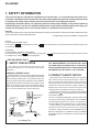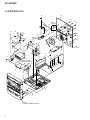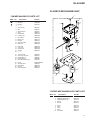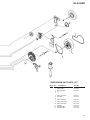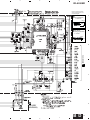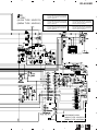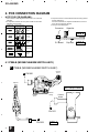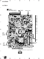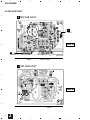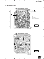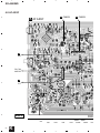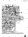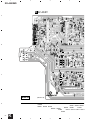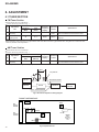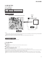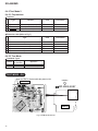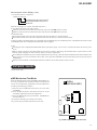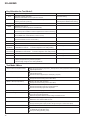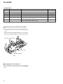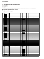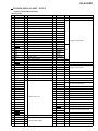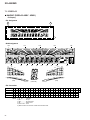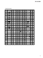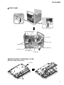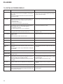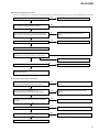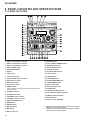
1
STEREO CD MD CASSETTE DECK RECEIVER XR-A550MD
MD
3
FREQ/
STATION
NR
ON/OFF
ASES
MD
REC/STOP
TAPE
REC/STOP
DISP
/CHARA
EJECT
MENU
DELETE
STEREO CASSETTE DECK
MINIDISC
FULL LOGIC AUTO REVERSE
REC/PLAY
ORDER NO.
RRV2107
COMPACT MINI COMPONENT
XR-A550MD
THIS MANUAL IS APPLICABLE TO THE FOLLOWING MODEL(S) AND TYPE(S).
Type
Model
XR-A550MD
Power Requirement
KUCXJ
AC120V
DBDXJ
AC110-127V/220-230V/240V
The Voltage can be converted by
the following method.
With the voltage selector
CONTENTS
1. SAFETY INFORMATION ...................................... 2
2. EXPLODED VIEWS AND PARTS LIST ................ 3
3. SCHEMATIC DIAGRAM ..................................... 16
4. PCB CONNECTION DIAGRAM .......................... 42
5. PCB PARTS LIST ............................................... 62
6. ADJUSTMENT .................................................... 70
7. GENERAL INFORMATION ................................ 92
7.1 PARTS .......................................................... 92
7.1.1 IC ........................................................... 92
7.1.2 DISPLAY ................................................ 94
7.2 DIAGNOSIS .................................................. 96
7.2.1 DISASSEMBLY ..................................... 96
7.2.2 DETAILS OF ERROR DISPLAY ......... 102
7.2.3 TROUBLESHOOTING ........................ 104
7.3 BLOCK DIAGRAM ...................................... 109
8. PANEL FACILITIES AND SPECIFICATIONS .. 112
PIONEER ELECTRONIC CORPORATION
4-1, Meguro 1-Chome, Meguro-ku, Tokyo 153-8654, Japan
PIONEER ELECTRONICS SERVICE, INC. P.O. Box 1760, Long Beach, CA 90801-1760, U.S.A.
PIONEER ELECTRONIC (EUROPE) N.V. Haven 1087, Keetberglaan 1, 9120 Melsele, Belgium
PIONEER ELECTRONICS ASIACENTRE PTE. LTD. 253 Alexandra Road, #04-01, Singapore 159936
c PIONEER ELECTRONIC CORPORATION 1999
T – IZE MAR. 1999 Printed in Japan
XR-A550MD
1. SAFETY INFORMATION
This service manual is intended for qualified service technicians ; it is not meant for the casual do-ityourselfer. Qualified technicians have the necessary test equipment and tools, and have been trained
to properly and safely repair complex products such as those covered by this manual.
Improperly performed repairs can adversely affect the safety and reliability of the product and may
void the warranty. If you are not qualified to perform the repair of this product properly and safely, you
should not risk trying to do so and refer the repair to a qualified service technician.
WARNING
This product contains lead in solder and certain electrical parts contain chemicals which are known to the state of California to cause
cancer, birth defects or other reproductive harm.
Health & Safety Code Section 25249.6 – Proposition 65
NOTICE
(FOR CANADIAN MODEL ONLY)
Fuse symbols
(fast operating fuse) and/or
be of identical designation.
(slow operating fuse) on PCB indicate that replacement parts must
REMARQUE
(POUR MODÈLE CANADIEN SEULEMENT)
Les symboles de fusible
(fusible de type rapide) et/ou
de remplacement doivent avoir la même désignation.
(fusible de type lent) sur CCI indiquent que les pièces
(FOR USA MODEL ONLY)
1. SAFETY PRECAUTIONS
The following check should be performed for the
continued protection of the customer and service
technician.
ANY MEASUREMENTS NOT WITHIN THE LIMITS
OUTLINED ABOVE ARE INDICATIVE OF A POTENTIAL
SHOCK HAZARD AND MUST BE CORRECTED BEFORE
RETURNING THE APPLIANCE TO THE CUSTOMER.
LEAKAGE CURRENT CHECK
Measure leakage current to a known earth ground (water
pipe, conduit, etc.) by connecting a leakage current tester
such as Simpson Model 229-2 or equivalent between the
earth ground and all exposed metal parts of the appliance
(input/output terminals, screwheads, metal overlays, control
shaft, etc.). Plug the AC line cord of the appliance directly
into a 120V AC 60Hz outlet and turn the AC power switch
on. Any current measured must not exceed 0.5mA.
Reading should
Leakage not be above
current 0.5mA
tester
Device
under
test
Test all
exposed metal
surfaces
Also test with
plug reversed
(Using AC adapter
plug as required)
AC Leakage Test
2
Earth
ground
2. PRODUCT SAFETY NOTICE
Many electrical and mechanical parts in the appliance
have special safety related characteristics. These are
often not evident from visual inspection nor the protection
afforded by them necessarily can be obtained by using
replacement components rated for voltage, wattage, etc.
Replacement parts which have these special safety
characteristics are identified in this Service Manual.
Electrical components having such features are identified
by marking with a on the schematics and on the parts list
in this Service Manual.
The use of a substitute replacement component which does
not have the same safety characteristics as the PIONEER
recommended replacement one, shown in the parts list in
this Service Manual, may create shock, fire, or other hazards.
Product Safety is continuously under review and new
instructions are issued from time to time. For the latest
information, always consult the current PIONEER Service
Manual. A subscription to, or additional copies of, PIONEER
Service Manual may be obtained at a nominal charge from
PIONEER.
XR-A550MD
2. EXPLODED VIEWS AND PARTS LIST
NOTES:
• Parts marked by "NSP" and can not be supplied.
• The mark found on some component parts indicates the importance of the safety factor of the part.
Therefore, when replacing, be sure to use parts of identical designation.
• Screws adjacent to mark on the product are used for disassembly.
2.1 PACKING
KUCXJ
Type Only
12
9(1/2)
V
LO
EK
CF
S
EL
PE
OP
W
RE
YA
SS
LP
SI
AB
OA
RA
KUCXJ
Type Only
K
CS
CS
CS
XU
S
.P
D
ID
ID
ID
C
EL
RA
DBDXJ
Type Only
P
G
M
A
ER
EP
TA
AR
DN
MO
NO
M
NO
O
AB
DN
1
UC
X0R
52
NU
TI
ITA
TS
C
NO
RT
LO
ER
OM
ET
2
4
5
15
7
16
3
13
14
6
9(2/2)
8(1/2)
11
10
8(2/2)
(1) PACKING PARTS LIST
Mark No.
1
2
3
4
Description
Part No.
FM Antenna
Operating Instructions
(English/French)
AM Loop Antenna
Remote Control Unit
(CU-XR054)
ADH7004
See Contrast table (2)
Battery Cover
Dry Cell Battery (R6P, AA)
Catalog Bag
(0.03 × 230 × 340)
Front Pad
AZA7204
VEM-013
Z21-038
XTB3001
XZN3046
Mark No.
NSP
NSP
NSP
5
6
7
8
Description
Part No.
9
10
11
12
13
Rear Pad
Packing Case
Packing Sheet
Warranty Card
Power Cord
XHA3004
See Contrast table (2)
AHG7049
See Contrast table (2)
See Contrast table (2)
14
15
Polyethylene Bag
Operating Instructions
(Chinese/portuguese)
Operating Instructions
(English/Spanish)
AHG7033
See Contrast table (2)
16
See Contrast table (2)
XHA3003
(2) CONTRAST TABLE
XR-A550MD/KUCXJ and DBDXJ are constructed the same except for the following :
Mark No.
NSP
Symbol and Description
KUCXJ Type
Part No.
DBDXJ Type
2
10
12
13
15
Operating Instructions (English/French)
Packing Case
Warranty Card
Power Cord
Operating Instructions (Chinese/Portuguese)
XRE3021
XHD3078
ARY7023
ADG7022
Not used
Not used
XHD3079
Not used
ADG1158
XRC3011
16
Operating Instructions (English/Spanish)
Not used
XRE3022
Remarks
3
XR-A550MD
2.2 EXTERIOR (1/2)
15
8
9
15
11
11
14
KUCXJ Type
Only
9
11
Note : Attatch on the same numbers × three
12
12
9
19
1
2
Refer to
"2.5 $M MECHA CD DIGITAL ASSY
6
20
4
19
10
5
13
3
7
4
XR-A550MD
(1) EXTERIOR (1/2) PARTS LIST
Mark No.
NSP
NSP
1
2
3
4
5
Description
Part No.
22P F.F.C/30V
$M MECHA CD DIGITAL Assy
Volume Knob
FL Cover A
FL Cover C
XDD3018
XXA3006
XAA3005
See Contrast table (2)
XAK3071
6
7
8
9
10
Tray Cap
Display Panel
Bonnet Case
Screw
Pioneer Badge
XAK3075
See Contrast table (2)
XZN3001
BPZ30P100FZK
XAM3001
11
12
13
14
15
Screw
Disc Label
Jog Knob Assy
65 Label
Screw
VBT30P080FZK
XAX3127
XXG3023
See Contrast table (2)
BCZ30P080FZK
16
17
18
19
20
•••••
•••••
•••••
Cushion Rubber
Tray Cap Assy
XEB3002
XXG3031
(2) CONTRAST TABLE
XR-A550MD/KUCXJ and DBDXJ are constructed the same except for the following :
Mark No.
4
7
14
Symbol and Description
FL Cover A
Display Panel
65 Label
Part No.
KUCXJ Type
DBDXJ Type
XAK3093
XAK3057
ARW7050
Remarks
XAK3026
XAK3064
Not used
5
XR-A550MD
2.3 EXTERIOR (2/2)
15
19
19
29
24
KUCXJ
Type Only
28
19
32
18
26
19
22
16
24
7
11
24
19
25
3
DBDXJ
Type Only
33
21
24
6
2
31 18
17
19
19
23
14
13
12
5
19
9
19
Refer to "2.7 MD
MECHANISM ASSY".
19
20
27
10
20
19
8
19
Refer to
"2.4 FRONT PANEL SECTION".
6
30 4
1
XR-A550MD
(1) EXTERIOR (2/2) PARTS LIST
Mark No.
1
2
3
4
5
NSP
Description
Part No.
Mark No.
Description
Part No.
AF Assy
SECONDARY Assy
PRIMARY Assy
FM/AM TUNER MODULE
Power Transformer (T1)
See Contrast table (2)
See Contrast table (2)
See Contrast table (2)
AXQ7065
See Contrast table (2)
16
17
18
19
20
MD MAIN Assy
Fan Plate
Push Rivet
Screw
M3 Plastic Screw
See Contrast table (2)
ANG7153
AEC7149
VBZ30P080FZK
XBB3001
6
7
8
9
10
DC Fan Motor
Fuse (FU1)
Chassis
MD Mechanism Assy
MD Bracket R
AXM7003
See Contrast table (2)
XNA3002
AXA7054
XNG3011
21
22
23
24
25
Screw
Cord Clamper
MD SUB Assy
Screw
Connector Assy 9P
ASZ40P060FMC
RNH-184
See Contrast table (2)
BPZ30P100FZK
XDE3008
11
12
13
14
15
PCB Bracket
MD Bracket L
Heat Sink
Wire Clip
Rear Panel
XNG3006
XNG3010
XNH3003
XEC3002
See Contrast table (2)
26
27
28
29
30
Connector Assy 3P
Separation Sheet
Screw
SUB TRANS Assy
Binder
XDE3024
XEC3010
BBZ30P300FMC
See Contrast table (2)
ZCA-SKB90BK
31
32
33
PCB Spacer
Fuse Caution Label
Fuse (FU2, FU3 : T1.6A)
AEC7080
See Contrast table (2)
See Contrast table (2)
NSP
(2) CONTRAST TABLE
XR-A550MD/KUCXJ and DBDXJ are constructed the same except for the following :
Mark No.
1
2
3
5
7
Symbol and Description
Part No.
KUCXJ Type
DBDXJ Type
AF Assy
SECONDARY Assy
PRIMARY Assy
Power Transformer (T1)
Fuse (FU1 : 4A)
XWZ3172
XWZ3173
XWZ3175
XTS3030
REK1082
XWZ3181
XWZ3182
XWZ3184
XTS3028
Not used
7
15
16
23
29
Fuse (FU1 : T3.15A)
Rear Panel
MD MAIN Assy
MD SUB Assy
SUB TRANS Assy
Not used
XNC3031
XWZ3177
XWZ3179
XWZ3176
AEK1059
XNC3032
XWZ3186
XWZ3188
XWZ3185
32
33
Fuse Caution Label
Fuse (FU2, FU3 : T1.6A)
XAX3132
Not used
Not used
AEK1056
Remarks
7
XR-A550MD
2.4 FRONT PANEL SECTION
17
26
22
17
17
40
6
18
1
13
34(1/2)
10
35
15
17
23
34(2/2)
7
24
36
25
29
2
17
37
8
4
17
41
19
17
3
11
17
16
9
38
30
39
17
21
20
12
Refer to
"2.8 MECHANISM UNIT".
14
32
27
33
28
8
31
XR-A550MD
(1) FRONT PANEL SECTION PARTS LIST
Mark No.
Description
Part No.
Mark No.
Description
Part No.
1
2
3
4
5
DISPLAY Assy
MD FRONT Assy
MD LED Assy
Flexible Cable 11P
•••••
See Contrast table (2)
See Contrast table (2)
See Contrast table (2)
XDD3020
21
22
23
24
25
Damper Assy
Flap Holder
Front Panel Assy
Function Button
CD Button
AXA7052
XMR3004
XXG3018
XAD3020
XAD3010
6
7
8
9
10
Flexible Cable 13P
Flexible Cable 11P
Flexible Cable 38P
Connector Assy 5P
MD Lens
XDD3021
XDD3019
XDD3004
XDE3002
XAK3073
26
27
28
29
30
Eject Button
FL Window MD
Deck Lens R
Jog Lens
FL Cover MD
XAD3023
XAK3070
XZN3063
XAK3025
XAK3072
11
12
13
14
15
Deck Bracket
Mechanism Unit
LT Conductor
Door Spring R
MD Flap
XNG3013
XYM3004
XAK3074
XBH3002
AAN7186
31
32
33
34
35
Deck Door R
Front Panel
Sub Panel A
Power Button
Play Button
XAN3009
XMB3015
XAK3046
XAD3007
XAD3022
16
17
18
19
20
Latch Spring R
Screw
MD Spring
Latch Mold R
GND Plate C
ABH7131
BPZ30P100FZK
ABH7154
XMR3002
XNG3012
NSP
NSP
36
37
38
39
40
S.C. Button
TIMER Button
FL Cover D
Screw
Cushion A
XAD3009
XAD3016
See Contrast table (2)
PCZ20P040FMC
PED1001
NSP
41
Cord with Plug
DE007VE0
NSP
NSP
(2) CONTRAST TABLE
XR-A550MD/KUCXJ and DBDXJ are constructed the same except for the following :
Mark No.
1
2
3
38
Symbol and Description
DISPLAY Assy
MD FRONT Assy
MD LED Assy
FL Cover D
Part No.
KUCXJ Type
DBDXJ Type
XWZ3174
XWZ3178
XWZ3180
XAK3094
Remarks
XWZ3183
XWZ3187
XWZ3189
XAK3092
9
XR-A550MD
2.5 $M MECHANISM CD
Refer to "2.6 SERVO MECHANISM ASSY".
8
21
25
7
22
14
24
13
23
11
1
5
2
26
12
15
29
18
27
19
28
16
6
29
17
10
29
3
30
29
29
29
29
9
29
29
10
XR-A550MD
2.6 SERVO MECHANISM ASSY
• $M MECHANISM CD PARTS LIST
Mark No.
NSP
Description
1
9
Part No.
1
2
3
4
5
MOTOR Assy
SW Assy
CD Assy
•••••
Servo Spring
AWZ8428
AWZ8429
XWZ3141
6
7
8
9
10
Belt
Clamp Magnet
Yoke
Mecha Base
Loading Tray
AEB7072
AMF7001
ANB7067
ANW7125
ANW7088
11
12
13
14
15
Servo Base
Rotary Tray
Clamper
Clamper Holder
Main Cam
ANW7089
ANW7113
ANW7091
ANW7092
ANW7093
16
17
18
19
20
Gear Pully
Lock Lever
Planet Gear
Actuater
•••••
ANW7094
ANW7095
ANW7096
ANW7097
21
22
23
24
25
15P F.F.C/30V
Connector Assy (6P)
Float Rubber A
Float Rubber B
Servo Mechanism Assy
ADD7038
ADE7010
AEB7063
AEB7066
AXA7039
26
27
28
29
30
Screw
Carriage Motor
Motor Pulley
Ha Narl
Cushion Rubber
IPZ30P080FMC
VXM1033
PNW1634
GEM1016
XEB3003
7
9
9
ABH7126
9
4
5
8
6
3
10
2
• SERVO MECHANISM ASSY PARTS LIST
Mark No.
1
2
3
4
5
6
7
8
9
10
Description
Part No.
Servo Mechanism
SPINDLE MOTOR Assy
SLEAD MOTOR Assy
Gear A
Gear B
AXA7039
AEA7009
AEA7010
AEA7013
AEA7014
Screw
Screw
Screw
Screw
Leaf Switch
AEA7015
AEA7016
AEA7017
AEA7018
AEA7011
11
XR-A550MD
2.7 MD MECHANISM ASSY
68
16
66
35
45
8
12
10
5
11
18
64
63
66
27
29
39
30
40
B1
64
13
37
A1
62
41
25
B2
3
9
33
22
21
A2
19
65
38
57
65
23
63
26
17
57
57
37
20
31
60
51
42
62
1
52
49
50
4
62
62
47
PWB-B
6
38
57
48
15
59 x2
32
43
7
14
24
28
PWB-A
59 x2
58
67 x4
34
66
58
46
B2
A1
B1
A2
2
55
54
53
61 x3
12
66
36
XR-A550MD
• MD MECHANISM ASSY PARTS LIST
Mark No.
1
2
3
4
5
Description
Part No.
Mark No.
Description
Part No.
Loading Gear Shaft
MD Guide (B)
Base Frame
Flat Cable 5P (CW1901)
Cartridge Holder
1242900108
1242000209
1242000210
1245120287
1242140138
36
37
38
39
40
Bottom Cover
Cushion (A)
Cushion (B)
Cushion
Magnet Head
1243230028
1243260020
1243260021
1243260097
1246100008
6
7
8
9
10
Cam Plate Lever
H/A Shift Arm
Holder Arm
Roller Arm Lever
Clamper Lever
1242480122
1242480123
1242480124
1242480125
1242480126
41
42
43
44
45
Pickup
MD Flexible Cable (24P)
Connector Assy
•••••
Head Guard Sheet
1246170019
1245120301
1245120299
11
12
13
14
15
Catch
Slider Lever
Roller Holder Spring
Spring
Shift Arm Spring
1242480127
1242480128
1242580157
1242580159
1242580053
46
47
1242070047
1245210149
48
49
Drive Chassis
PWB-B
(MD Mechanism Switch Assy)
Push Switch (SW1956)
Push Switch (SW1954)
16
17
18
19
20
Holder Arm Spring
Rack Spring
Catch Spring
Spring (A)
Drive Shaft Spring
1242580054
1242580055
1242580094
1242580160
1242580161
50
51
52
53
54
Push Switch (SW1955)
Push Switch (SW1952)
Slide Switch (SW1953)
Spindle Motor (M901)
Sled Motor (M902)
1245300026
1245300027
1305301315
1246300048
1246300049
21
22
23
24
25
Roller Arm Spring
Loading Gear (B)
Drive Gear
Loading Gear (A)
Roller Gear
1242580093
1242810063
1242810064
1242810065
1242810066
55
56
57
58
59
Loading Motor (M903)
•••••
Screw
Screw
Screw
1246300050
1249700161
1249700162
1249700163
26
27
28
29
30
Rack Gear
Connector 2P (CN1903)
PWB-A (MD Main Assy)
Roller Holder
Transfer Roller
1242810067
1245120288
1246840167
1242860001
1242870014
60
61
62
63
64
Screw
Screw
Screw
Screw
Washer
1249700061
1249700065
1249700076
1249700108
1249900005
31
32
33
34
35
Drive Shaft
Pickup Guide Shaft
MD Guide (A)
Pickup Slide Shaft
Top Cover
1242900105
1242900040
1242000208
1242900039
1243230027
65
66
67
68
Washer
Screw
Screw
Screw
1249900006
1189700020
1249700077
1249700011
1244030163
1245300025
1245300026
13
XR-A550MD
2.8 MECHANISM UNIT
2
9
10
12
13
1
14
XR-A550MD
5
6
8
11
• MECHANISM UNIT PARTS LIST
Mark No.
Description
Part No.
1
1
2
3
4
Plate HD BLK
Plate HD BLK
Motor Main BLK
•••••
•••••
F513-811
F513-825
F525-324
5
6
7
8
9
Clutch Assy BLK
Main Belt
•••••
Clutch Assy BLK
Roller Pinch BLK R
F522-037
FF17G-31
F522-045
F514-129
10
11
12
13
Roller Pinch BLK L
F/R Belt
Plate Base BLK
Plate Base BLK
F514-130
FF18W-12
F512-127
F512-128
15
1
2
3
4
XR-A550MD
3. SCHEMATIC DIAGRAM
3.1 OVERALL WIRING DIAGRAM
A
DECK I
R/P HEAD
ERASE
L R HEAD
O DISPLAY ASSY
DECK MECHA
(KUCXJ TYPE : XWZ3174)
(DBDXJ TYPE : XWZ3183)
K K 1/3 K 3/3
B
AF ASSY
(KUCXJ TYPE : XWZ3172)
(DBDXJ TYPE : XWZ3181)
A
FM/AM TUNER
MODULE (AXQ7065)
C
L
D
CD ASSY (XWZ3141)
C
MOTOR
ASSY
(AWZ8428)
D
SW ASSY
(AWZ8429)
SERVO MECHANISM ASSY
(AXA7039)
$M MECHA CD DIGITAL ASSY(XXA3006)
T1
POWER
TRANSFORMER
KUCXJ TYPE : XTS3030
DBDXJ TYPE : XTS3028
B
SECONDARY ASSY
(KUCXJ TYPE : XWZ3173)
(DBDXJ TYPE : XWZ3182)
M
PRIMARY ASSY
(KUCXJ TYPE : XWZ3175)
(DBDXJ TYPE : XWZ3184)
16
1
2
3
4
5
6
7
8
XR-A550MD
Note : When ordering service parts, be sure to refer to "EXPLODED VIEWS and PARTS LIST" or "PCB PARTS LIST".
I
MD LED ASSY
(KUCXJ TYPE : XWZ3180)
(DBDXJ TYPE : XWZ3189)
A
H
MD FRONT ASSY
(KUCXJ TYPE : XWZ3178)
(DBDXJ TYPE : XWZ3187)
MD MECHANISM ASSY
(AXA7054)
(MD MAIN ASSY)
E PWB-A
(1246840167)
PWB-B (MD MECHANISM
SWITCH ASSY)
(1245210149)
CN1902
F
B
CN1904
CN3331
C
G
J
MD MAIN ASSY
(KUCXJ TYPE : XWZ3177)
(DBDXJ TYPE : XWZ3186)
MD SUB ASSY
(KUCXJ TYPE : XWZ3179)
(DBDXJ TYPE : XWZ3188)
J3651
N
XDE3024
SUB TRANS ASSY
(KUCXJ TYPE : XWZ3176)
(DBDXJ TYPE : XWZ3185)
AXM7003
D
NEUTRAL
AN1
LIVE
Y2
AC POWER CORD
KUCXJ TYPE : ADG7022
DBDXJ TYPE : ADG1158
FU1
Y1
17
5
6
7
8
1
2
3
4
XR-A550MD
3.2 FM/AM TUNER MODULE
A
MIX AMP
1T378A
RF AMP
OSC
1T378A
BUFFER
B
IF AMP
FM +B SW
C
MW RF TUNING BLOCK
AXX7041
FM/AM TUNER MODULE
(AXQ7065)
D
18
A
1
2
3
4
5
6
7
8
XR-A550MD
A
CN3051
B
K 2/3
AF AMP
AF AMP
REGULATOR
C
PLL
D
5
6
7
A
8
19
1
2
3
4
XR-A550MD
3.3 CD, MOTOR and SW ASSEMBLIES
A
R8123
56k
B
C
B
CD ASSY
(XWZ3141)
C MOTOR ASSY
(AWZ8428)
CARRIAGE MOTOR
D
J8503
D20PWW0405E
SERVO MECHANISM ASSY (AXA7039)
20
B C
1
2
3
4
5
6
7
8
XR-A550MD
1
Note: The encircled numbers
denote measuring point in the
schematic diagram.
2
1
A
CN8005- Pin 1 :
PLAY MODE (RF)
H : 500nsec/div
C8371
100/10
1.8Vp-p
VREF
2 CN8005- Pin 2 :
1.0Vp-p
VREF
VREF:CN8005- Pin3
B
K 2/3
CN1052
C8307
1000p
YB
H : 5msec/div
L8371 47µH
YB
C8308
1000p
0.047
TEST MODE,
Tracking Open(TRER)
C8256 0.1
C8255 0.1
C
2SB1237X
2SB1237X
2SD1858X
2SD1858X
0.047
C8257
0.1
D
D
SW ASSY
(AWZ8429)
J8502
5
6
7
B D
8
21
1
2
3
4
XR-A550MD
3.4 PWB-A (MD MAIN ASSY) and PWB-B (MD MECHANISM SWITCH ASSY)
E PWB-A (MD MAIN ASSY)(1246840167)
TP1141
TP1275
ADIPO
TP1140
R1155
56K
TP1139
TP1274
4
34
ADLPFO
DIFF
33
TP1138
28
BOUT
20
21
22
23
24
LATCH
C1105
1
DATA
19
DVCC
18
25
TP1136 R1154
22K
TP1135 R1153
22K
TP1134 R1152
22K
TP1133 R1151
22K
TP1132 R1150
22K
11
C1211
1
12
13
14
15
16
TP1220
FODRF
FODRR
TRDRF
TRDRR
SLDRF
SLDRR
SPDRF
SPDRR
R1653
100K
R1651
R1657
R1655
R1661
R1659
R1665
17
100K
120K
120K
82K
82K
62K
18
19
20
21
22
23
24
25
R1663
62K
ENCOD
X176KO
FODRF
FODRR
TRDRF
TRDRR
SLDRF
SLDRR
SPDRF
SPDRR
26 27 28
26 27 28 29 30 31 32 33 34 35 3
DATA
17
LATCH
16
26
FOUT
CLOCK
15
CLOCK
14
DTEMP
13
DTEMP
FIN
27
EOUT
LOGIC
10
WBO-I
99 98
100
C1210
1
EIN
RF2
12
BIN
DGND
11
AOUT
SGAIN
10
AIN
R1102 TP1137
560
29
TCG
BOUT-IN
FOUT-IN
WBO-I
30
TCGO
DISC
9
HPF
TCGI
STBY
8
LPF
BIAS
AVCC
R1105
390K
7
TCG
BOUT-IN
FOUT-IN
5
31
WBO
RFADD
BIAS
C1104
0.027
22KI
RF PROCESSOR
REFO
AGND
6
32
AOUT-IN
EOUT-IN
99 98 97 96 95 94 93 92 91 9
EFMMON
AVCC
EFMI
AGND
AIN
EIN
TCG
BIN
FIN
VBAT
WBI
VDD1
DGND
TEST0
TEST1
TEST2
11
10
TP1129
TP1130
A4
A5
A6
A7
A8
C1103
1
22KO
ADIP
AGC
C1202
1
AOUT-IN
EOUT-IN
C1116
C1115270P(CH)
C1114 270P(CH)
C1113 270P(CH)
C1112 270P(CH)
270P(CH)
IC1101
IR3R55
EFMO-I
EFMO-I
1
2
3
4
5
6
7
8
9
RAA3
RAA2
RAA1
ADIPI
SYD7
SYD6
SYD5
SYD4
SYD3
SYD2
SYD1
SYD0
100
36
SYRS
SYRDX
SYWRX
37
RAA0
RAA10
VDD2
RAA4
RAA5
RAA6
RAA7
RAA8
38
ADAGI
ADAGC
EFMO
39
RF2-1
AVCC
40
35
REFI
5
RF1
FIN
EIN
RF3
RF4
EFMAGC
EFM
AGC
41
DIFF
4
C1102
1
AIN
42
&
SW
3
RF3
43
TP1142
C1106
0.47
A3
A2
A1
A0
2
RF4
BIN
EFMAGI
R
RF1
44
EFMI
1
45
AGND
46
ATTR
RF2
47
GOUT
48
1
TP1131
C1107
0.0047
C1109
1
C1111 C1110
0.015
0.47
POUT
A
SYRS
SYRD
SYWR
SYD7
SYD6
SYD5
SYD4
SYD3
SYD2
SYD1
SYD0
R1211
220
TP1150
B
TP1215
C1121
1
1
C1206
1
R/P
R/P
VCC
L1101
10µH
L1102
0.47µH
R1166
1.2K
C1145
0.033
A4
R1100
27
1
FN
TP
FP
TN
9 8 7 6 5 4 3 2 1
CN1603
1
1
–
2
2
SP+
SP–
TP1608
TP1609
22
E F
1
VREFO
VM3+
OUT4
IC1601
M56758FP
5ch MOTOR DRIVER
65
64
R1422
10K
TP1455
TP1456
TP1457
R1430
10K
TP1404
TP1458
R1429
10K
AVCC
VREF
HINF
GND
TESTK2
TESTK1
MINF
DTEMP
AVCK1
AVCK2
AVCK3
TEST0
TEST1
TEST2
DOUTMT
MUTE
DAMUT
EMPH
ADMUT
SYSD5
SYSD4
49 50
DATA
LATCH
CLOCK
R/P
TP1413
TP1414
TP1415
C1406
1
62
61
60
59
58
R1476
1K EE
EE
EP
R1474 P
1K
56
55
SYSD0
SYSD1
SYSD2
SYSD3
54
53
52
51
SYD0
SYD1
SYD2
SYD3
TP1454
C1424
0.022
67
66
SYRS
SYRD
SYWR
SYD7
SYD6
SYD5
SYD4
C1403
680P
SPDRR
TP1416
57
VM4–
SLP
SLN
1
2
3
Q1403
RN2404
SLDRR
Q1402
RNC1404
3
2
2
3
1
Q1401
RN2404
1
Q1404
RNC1404
R1667
22K R1666
22K
R1669
6.8K
3
R1416
10K
IC1402
S29294A
5
6
7
8
DI
SK
DATA CS
GND VCC
PRTCT
2
4
3
2
1
E -PROM
SLDRF
23
22
3
1
TP1612
C1661
100/10
L1601
1µH
For details regarding schematic diagram caution items, refer to page 24.
2
72
63
32
2
IN5+ 25
IN4+ 24
IN4–
73
70
STID
C1657
0.0056
SPN
SPP
VM4+
VM5+
28
OUT5 27 VM5–
IN5–
26
19 SS.GND
VREF
20
74
71
SPDRF
C1602
4.7
32
29
18 MUTE2
77
76
75
4
EEPK
EPCS
33
30
VM2–
OUT2
IN2–
L3CLK
L3MODE
L3DATA
GND
VCC
EEPK
EEPD
EPCS
EEPRO
R1414 PRO
10K EEPD
GND
VM2+
R1662
10K
R/P
VM3–
34
VM1+
78
31 32 33 34 35 36 37 38 39 40 41 42 43 44 45 46 47 48 49 50
J1405
10K
R1664
10K
36
35
IN2+
17 MUTE1
R1650
10K
38
37 IN3+
OUT1
30
79
68
S2
S1
SYRS
SYRD
SYWR
SYSD7
SYSD6
29
VREF
Vm2
16
C1631
1
TRY+
TRY–
TP1611
C1609
1
SPN
SPP
SLP
SLN
CN1604
1
1
2
2
–
28
XRST
80
39
13
15
C1656
0.0056
OUT3
41
IN3–
40
VBS2
31
14
R1652
10K
+
–
1.25V
IN1+
12
21
TP1610
M
27
R1409
1K
FODRR
FODRF
REGB
VBS1
42
R1658 15K
C1655 0.015
R1660 15K
LD+
LD–
C1651
820P(J)
TP1607
TP1606
C1650
820P(J)
+
SLD+
SLD–
CH3IN
C1654
0.015
10
REG+
VREF
TN T– C1652
TP T+ 820P(J)
CN1602
1
1
2
2
+
25
26
CIN
R1668
6.8K
C1601
4.7
1
2
3
4
Vm1
5
IN1–
6
7
VM1–
8
9
11
M903
MD
LOADING MOTOR
24
R1407
3.3K
LD+
LD–
R1611
12K
GND
TRDRF
TRDRR
R1654
6.8K
16
C1653
820P(J)
R1656
6.8K
PWB-B
MD MECHANISM
SWITCH ASSY
(1245210149)
FP F+
FN F–
M
R1428
1K
C1401
0.047
LOADING
HDON
R1614
18K
DINT
DSENSE
ST-ID
SERCH
MDRSW
FSW
VARI-P SW
P-DOWN
HDON
LD+
LD–
31
CIN
INNER
R1471
FOK 10K
R1613
27K
VSS
MCCK
VCC
C1407
0.022
R1610
30K
C1604
56P(CH)
INNSW
15
M902
MD
THREAD MOTOR
21
R1418
47K
69
IC1401
IX0232
MD SYSTEM
MICRO-COMPUTER
DATA
LATCH
R1617
47K
SW1956
–
19
SERCH
C1605
100/10
SW1955
M
18
23
C1610
10
R1609
1.5K
LOAD IN
ERROR
BYTE
CNVSS
STID OUT
SEACH OUT
RESET
17
DINT
DSENSE
C1412
680P
TP1616
Q1601
2SA1314C
LOADING
D
16
22
R1904
820
+
15
20
R1612
56K
M901
MD
SPINDLE MOTOR
14
MCCK
XRST
DIGCD
DIGEX
DFS1
DFS0
DAPON
ADPON
A/B
LDON
PCNT1
PCNT0
82 81
13
LOADIN
RECORDING
F
12
R1423
10K
R1424
10K
LDVAR
ADJS
CLOCK
DSTB
MDDATA
KDATA
DSCK
4M/16M
R/P
FOK
C1422
0.022
R1408
100K
LOADING
MINF
R1425
2.7K
RESET
R1412
100K
PLAYBACK
SW1954
TP1602
TP1601
R1903
820
SW1953
LEAD IN
HINF
R1413
3.3K
LEAD IN
10
11
TP1605
TP1604
C1421
0.022
CN1901
SW1952
R1901
470
LEAD IN
HINF
GND
LOADING
MINF
1
2
3
4
5
MINF
HINF
HDON
CN1601
R1902
1.8K
DILECT
1
2
3
4
5
R1406
3.3K
R1420
1K
VREF3.2V
99 98 97 96 95 94 93 92 91 90 89 88 87 86 85 84 83 82 81
DSTB
MDDATA
KDATA
DSCK
1 2 3 4 5 6 7
S
S Q1253
2SK1473
LEAD IN
HINF
GND
LOADING
MINF
9 8
1
2
3
4
5
6
7
8
9
C1423
0.022
Q1254
D 2SK1473
G
TP1255
14 13 12 11 10
GND
D
Q1252
2SK2909
D1252
SB0209CP
S
R1472
47K
LDVAR
IC1251
74ACT02F
G
MD LIGHT PICKUP
G
R1427
4.7K
C
S
D
VCC
D
C1254
10
C1255
4.7
L.DVAR
Q1251
2SK2909
G
TP1405
R1404
1K
C1402
0.047
100
EFMO TP1260
R1251
10
TP1251
L.DON
LVV
REC HEAD
R1223
680
C1251
0.027
TP1252
APC
8
7
6
5
L1251
47uH
C1252
120P
(CH)
D1251
SB0209CP
GND
CN1252
VCC
EXT.C
R1426
1K
R1401
1K
R1415
1K
10
11
9
8
7
6
5
4
T.COOL
3
2
F.COOL
1
MINF
HINF
I/V
12
13
14
15
I/V
I/V
16
17
18
I/V
19
20
21
22
23
24
25
SW
+2.8V
B
LVVOUT
APCOUT
LDVCC
DGNG
DGND
LDON
LDVAR
A
COM
RF1
F
E
RF3
RF4
VCC
AGND
MP/R
RF2
APCIN
DGND
LVVIN
FT+
F+
T26
27
28
2 12
1
2
LDOUT
DTEMP
3
Flexible
PCB
1
2
3
4
LDVAR
LDON
28 27 26 25 24 23 22 21 20 19 18 17 16 15 14 13 12 11 10
CN1101
A4
A5
A6
A7
A8
TP1109
TP1108
TP1107
TP1106
TP1105
TP1104
TP1103
TP1102
TP1101
TP1116
TP1115
TP1114
TP1113
TP1112
TP1111
R1106
10K
TP1120
TP1119
TP1118
TP1123
TP1128
TP1127
TP1126
C1101 R1107
1
4.7
R1473
100K
C1405
0.1
5
6
7
8
XR-A550MD
7
SYD7
SYD6
SYD5
SYD4
SYD3
SYD2
SYD1
SYD0
RSTX
DGND
VDD1
DINTX
MCCK
COUT
SENSE
FOK
SFSY
SBSY
SBO
9
C1207
1
23 22
69
68
R1254
220
67
66
R1201
150
XL1201
C0001AW
C1204
12P(CH)
C1205
12P
(CH)
61
60
59
58
57
R1269
00
56
TP1273
55
53
R1263
10K
R1261
10K
52
C1954
15P
(CH) R1963
1.5K
1
2
3
4
5
6
7
8
R1962
220K
C1955
0.047
C1956
47/6.3
C1953
0.47
A9
RAS
WE
I/O2
I/O1
VCC
A3
A2
A1
A0
OE
CAS
I/O3
I/O4
GND
A4
A5
A6
A7
A8
16 17 18 19 20
L1203
4.7µH
L1201
0.47µH
11 12 13 14 15
C1958
0.047
14
R1969
56
Vcc
R1927
22 DOUTO TP1901
GND 7
6
5
4
3
2
1
1
2
3
4
TP1902
TP1904
R1974
220
CN1904
DIGOUT
GND
GND
DIGIN
G
CN4101
R1973
6.8K
C1927
0.047
B
IC1907
TC9246F
CLOCK
GENERATOR
Vcc
1
2
3
4
5
6
7 GND
A4
A5
A6
A7
A8
12
VDD 16 C1957
REF
100/6.3
LOCK 15
PD
S2 14
VDDA
S1 13
AMPI
M2 12
AMPO
M1 11
VSSA
CKO 10
XI
R1968
NC
VSS 9
220
5 4 3 2 1
IC1202
IX2474AF
4M bit D-RAM
10
11
8
R1221
220
A9
A3
A2
A1
A0
9 8 7 6
C1951
0.047
R1967
47
C1952
0.01
10
8
9
13
R1266
10K
51
AND GATE
IC1916
74VHC08F
TP1911
Vcc 5
1
2
3 GND
4
TP1279
54
TP1215
C1206
1
AND GATE
IC1906
TC7ST08F
(CH)
62
R1202
1M
C1913
22P
C1203
1
63
C1992
0.1
14
13
12
D1990
1SS372
11
10
9
8
C1991
10
C1990
1
IC1990
74AC04FS
INVERTER
C1711
0.01
24
DFCK
64
DADATA
ADDATA
LRCK
BCLK
65
R1961
100
TP1214
71
70
A9
A4
A5
A6
A7
A8
A3
A2
A1
A0
C1210
1
TP1212
TP1213
26 27 28 29 30 31 32 33 34 35 36 37 38 39 40 41 42 43 44 45 46 47 48 49 50
DADATA
ADDATA
DFCK
BCLK
LRCK
RC120
220
72
TP1713
TP1712
RAA0
RAA10
VDD2
RAA4
RAA5
RAA6
RAA7
RAA8
RAOEX
DGND
RACASX
RAD2
RAD3
RAA9
RARASX
RAWEX
RAD1
RAD0
TCRS
73
74
R1964
6.8K
48 49 50
26 27 28
75
ADDATA
DFCK
BCLK
LRCK
DGND
VDD3
DOUT
DIN
XO
XI
DGND
VDD1
VPD
VXI
CDBCLK
CDLRCK
CDDATA
TEST4
TEST3
TESO1
EXPORT1
EXPORT0
X700KO
R1965
10K
RAA3
RAA2
RAA1
X176KO
FODRF
FODRR
TRDRF
TRDRR
SLDRF
SLDRR
SPDRF
SPDRR
ACRCER
PLCK
EFMO
IC1201
LR37648A
ENCODE/DECODE/ATRAC
18
19
21
20
17
TP1216
FEMON
DADATA
A
C1964
0.001
SBCK
TEMON
TOTMON
SYRS
SYRDX
SYWRX
13 14
circuit and measure.
TP1210
TP1278
78 77 76
99 98
100
PWB-B
(MD MECHANISM SWITCH ASSY)
SW 1952: DIRECT
ON-OFF
SW 1953: LEAD IN
ON-OFF
SW 1954: PLAYBACK ON-OFF
SW 1955: RECORDING ON-OFF
SW 1956: LOADING
ON-OFF
270P
99 98 97 96 95 94 93 92 91 90 89 88 87 86 85 84 83 82 81 80 79 78 77 76
EFMMON
AVCC
EFMI
AGND
AIN
EIN
TCG
BIN
FIN
VBAT
WBI
VDD1
DGND
TEST0
TEST1
TEST2
100K
6 – 9 insert
TP1218
TP1217
XRST
C1209 DINT
1
MCCK
CIN
R1210
100 DSENSE
FOK
SYRS
SYRD
SYWR
SYD7
SYD6
SYD5
SYD4
SYD3
SYD2
SYD1
SYD0
TP1204
275
100
6
R1262
10K
C1208
0.047
R1281
47
R1211
220
: MD PLAYBACK SIGNAL
: MD RECORDING SIGNAL
R1712
100K
C1716
0.01
L3DATA
VREFD
VSSO
VOUTL
VDDO
VOUTR
AVDD
AVSS
TEST2
TEST3
DATAI
DATAO
WS
BCK
L3DATA
28 27 26 25 24 23 22 21 20 19 18 17 16 15
C1710
47/4
2V
IC1701
UDA1340
AD/DA CONVERTER
VSSA
VDDA
VINL
VREFA
VINR
VADCN
VADCP
TEST1
OVERFL
VDDD
VSSD
SYSCLK
L3MODE
L3CLK
C1709
0.047
65
64
62
61
60
59
58
R1476
1K EEPK
EEPD
EPCS
R1474 PRO
1K
55
54
53
52
51
46 47 48 49 50
R1711 C1720
39K
0.01
R1715
1K
1
R1716
3.3K
L3CLK
L3MODE
L3DATA
R1475
1K
AA.GND
µCON 3.2V
3
2
AA.GND
BUCKUP
BUCKUP
C1707
10/16
R1717
IC1802 820
NJM431U
R1947
47
REGULATOR
Q1820
2SA1162G
SYD0
SYD1
SYD2
SYD3
Q1821
RNC1407
3
2
VREF3.2V
TP1802
C1807
220/4
JC121
0.047
Q1807
2SA1314C
R1821
1
R1827
270
R1820
1
R1808
27K
R1809
390
PDOWN
4
1
R1939
1K
R1456
1K
3
LOADIN
RESET Q1451
RNC1407
2
R1452
3
3.3K
1
TP1505
STID
DSCK
TP1506
SERCH
TP1507
KDATA
TP1508
MDDATA
TP1509
DSTB
TP1510
SYWR
SYD7
SYD6
SYD5
SYD4
C1805
1
2
Q1822
RNC1407 2
1
1
5
TP1803
Q1804
2SA1162G
IC1801
XC62EP32
3
DATA CS
GND VCC
PRTCT
4
3
2
1
PCNT0
R1811
27K
2
R1463
10K
R1804
220K
R1473
100K
C1405
0.1
R1805
100K
2
E -PROM
C1904
0.33
R1801
1.8K
SK
R1810
1K
C1704
1
Q1801
2SA1314C
TP1801
C1803
10
DI
Q1806
RNC1404
3
R1806
12
R1807
12
1
C1802
100/10
5
6
7
8
EEPK
EPCS
REGULATOR
IC1402
S29294A
R1802
270
3
2
1
2
1
C1460
1
LR190
4.7µH
R1995
2.2K
3
Q1802
RN1406
R1731
47
R1735
47K
R1733
47
L1950 JC196
1µH
00
– 24 are waveform Nos. on page 25 and 26.
6
7
TP1519
10
11
12
14
15
16
17
18
19
20
TP1521
TP1522
TP1523
TP1524
C1729
220P
C1724
100P
(CH)
CJ172 C1722
220P 100P
(CH) (CH)
TP1516
TP1517
TP1520
R1994
2.2K
R1734
47K
CN1902
1
2
3
4
5
6
7
8
9
13
TP1518
R1708
4.3K
5
TP1511
TP1512
TP1515
C1801
2.2
P.GND
R1707
4.3K
1
C1425
0.047
TP1502
TP1503
TP1504
R1454 1K
R1458 6.8K
R1460 6.8K
R1462 6.8K
R1464 220
R1466 220
D.GND
PCNT0
Q1803
RN1406
TP1501
66
TP1413
TP1414
TP1415
C1406
1
TP1412
67
C
C1712
47/4
Q1701
2SC2412KR
BUCKUP
TP1416
L1701
10µH
TP1702
R1461 10K
R1459 10K
70
TP1454
SYSD5
SYSD4
R1714
39K
R1702
680K
R1701
1M
C1706
10/16
71
R1478
10K
LDON
56
SYWR
SYSD7
SYSD6
C1715
22/4
L3CLK
L3MODE
C1810
1
72
57
SYSD0
SYSD1
SYSD2
SYSD3
C1703
47/4
AA.GND
R1710
30K
73
63
49 50
L1702
10µH
74
69
VCC
EEPK
EEPD
EPCS
EEPRO
10 11 12 13 14
75
68
L3CLK
L3MODE
L3DATA
GND
R1713
39K
C1700
0.01
C1743
47/4
TP1710
78
C1714
47/4
79
77
76
C1806
10
EMPH
ADMUT
82 81
C1701
0.01
C1702
0.047
XRST
80
VREF3.2V
XRST
DIGCD
DIGEX
DFS1
DFS0
DAPON
ADPON
A/B
LDON
PCNT1
PCNT0
PCNT0
DOUTMT
MUTE
DAMUT
TP1701
TP1711
1 2 3 4 5 6 7 8 9
R1418
47K
85 84 83 82 81
C1713
22/4
R1424
10K
C1717
0.01
R1423
10K
JC171
00
AA.GND
21
22
23
24
MD FLEXIBLE PCB
PDOWN 1
BUCKUP
LOAD SW
RESET
MD-ST
DSCK
SERCH
KDATA
MDDATA
DSTB
D.GND
D.GND
D.GND
D.GND
DVDD
DVDD
AVCC
L IN
AA.GND
R IN
AD.GND
L OUT
AA.GND
R OUT
24
G
CN4002
D
JC170
00
E
8
23
XR-A550MD
Voltages of PWB-A (MD MAIN ASSY)
Q1801
PIN
NO.
E
C
B
VOLTAGE
5V
5V
43V
Q1802
PIN
NO.
E
C
B
VOLTAGE
0V
0V
0.15V
Q1803
PIN
NO.
E
C
B
VOLTAGE
0V
0V
3.1V
IC1907
PIN
NO.
1
2
3
4
5
6
7
8
9
10
11
12
13
14
15
16
VOLTAGE
3.95V
3.2V
3.3V
Q1820
PIN
NO.
E
C
B
VOLTAGE
3.2V
3.18V
2.4V
Q1821
PIN
NO.
E
C
B
VOLTAGE
0V
0V
3.08V
2.8V
2.6V
4.9V
2.6V
1.6V
0V
0V
4.9V
0V
2.2V
5V
5V
0V
3.2V
3.1V
5V
IC1990
PIN
NO.
1
2
3
4
5
6
7
8
9
10
11
12
13
14
VOLTAGE
1.45V
1.7V
1.45V
1.7V
1.45V
1.7V
0V
1.7V
1.45V
1.37V
1.7V
1.37V
1.7V
3.17V
Q1822
PIN
NO.
E
C
B
VOLTAGE
0V
0V
0.1V
Q1451
PIN
NO.
E
C
B
VOLTAGE
0V
3.18V
0.1V
Q1401
PIN
NO.
E
C
B
VOLTAGE
3.2V
3.2V
0V
Q1402
PIN
NO.
E
C
B
VOLTAGE
0V
0V
2.3V
Q1403
PIN
NO.
E
C
B
24
VOLTAGE
3.18V
0V
3.15V
IC1101
PIN
NO.
1
2
3
4
5
6
7
8
9
10
11
12
13
14
15
16
17
Q1807
PIN
NO.
E
C
B
VOLTAGE
IC1202
PIN
NO.
1
2
3
4
5
6
7
8
9
10
11
12
13
14
15
16
17
18
19
20
VOLTAGE
1.1V
1.1V
3V
2V
1.5V
1.8V
0.8V
2.4V
1.2V
3.2V
1.2V
2.5V
1.3V
1.7V
1.3V
2.2V
2.4V
1.2V
1.1V
0V
18
19
20
21
22
23
24
25
26
27
28
29
30
31
32
33
34
35
36
37
38
39
40
41
42
43
44
45
46
47
48
VOLTAGE
0.7V
0.7V
0.7V
0.7V
1.6V
1.6V
0.7V
1.6V
1.6V
1.6V
1.6V
1.6V
3.2V
3.2V
0V
Groove:3.2V
Pit:0V
Low-reflectance:
0V
High-reflectance:
3.2V
0V
0V
1.45V
3.2V
0V
0V
3.2V
1.78V
1.78V
1.35V
1.36V
1.6V
1.6V
1.6V
1.6V
1.6V
0V
1.6V
1.6V
0.3V
1.6V
1.6V
1.6V
1.6V
3.2V
0V
1V
1.6V
1.6V
0.7V
0.7V
PIN
NO.
1
2
3
4
5
6
7
8
9
10
11
12
13
14
15
16
17
18
19
20
21
22
23
24
25
26
27
28
29
30
31
32
33
34
35
36
37
38
39
40
41
42
43
44
45
46
47
48
49
50
IC1201
VOLTAGE PIN
NO. VOLTAGE
1.48V
51 58V
0V
52 0V
1.6V
53 0V
0V
54 58V
1.36V
55 0V
1.77V
56 0V
1.6V
57 3.2V
1.36V
58 3.2V
1.77V
59 3.2V
1.25V
60 3.17V
1.6V
61 0V
3.17V
62 3.17V
0V
63 0V
0V
64 1.3V
0V
65 1.3V
0V
66 DIC input:1.58V
1.45V
1.56V
1.62V
1.7V
1.5V
1.63V
1.53V
1.8V
1.4V
1.2V
2.5V
0.8V
1.8V
1.4V
3.2V
1.2V
2.5V
1.3V
1.7V
1.3V
2.2V
0V
2.4V
1.2V
1.1V
1.5V
2V
3V
1.1V
1.1V
0V
3V
1.56V
PLAY:0V
REC:1.5V
IC1801
Q1404
PIN
NO.
E
C
B
VOLTAGE
0V
3.15V
2.1V
Q1601
PIN
NO.
E
C
B
VOLTAGE
5.45V
4.4V
4.8V
PIN
NO.
1
2
3
4
5
VOLTAGE
0V
44V
3.2V
3.1V
0V
67
68
69
70
71
72
73
74
75
76
77
78
79
80
81
82
83
84
85
86
87
88
89
90
91
92
93
94
95
96
97
98
99
100
Other:0V
1.58V
3.17V
0V
1.5V
1.55V
1.5V
0V
1V
1.55V
1.8V
1.56V
0V
0V
3.16V
0V
0V
0V
1.5V
1.5V
3.1V
3.17V
0V
3.17V
0.5V
0.6V
0.4V
0.4V
0.4V
0.9V
0.7V
0.8V
3.16V
3.15V
0V
PIN
NO.
1
2
3
4
5
6
7
8
9
10
11
12
13
14
15
16
17
18
19
20
21
22
23
24
25
26
27
28
29
30
31
32
33
34
35
36
37
38
39
40
41
42
43
44
45
46
47
48
49
50
IC1401
VOLTAGE PIN
NO. VOLTAGE
0V
51 0V
0V
52 0V
0.2V
53 0V
3.2V
54 0V
0V
55 0V
0V
56 0V
3.1V
57 0V
0V
58 0V
0V
59 3.2V
0V
60 0V
0V
61 3.2V
3.18V
62 3.2V
144V
63 0V
0V
64 0V
1.5V
65 3.2V
3.2V
66 3.2V
3.2V
67 3.2V
3.1V
68 0V
0V
69 0V
0V
70 3.1V
0V
71 0V
3.15V
72 3.1V
3.2V
73 97A:0V
0V
3.2V
3.2V
0V
0V
2V
3.2V
0V
3.2V
0V
0.8V
2.2V
0.2V
2.3V
0V
PLAY:3.15V
REC:0V
0V
0V
0V
3.2V
0V
0V
3.15V
0V
0V
0V
0V
74
75
76
77
78
79
80
81
82
83
84
85
86
87
88
89
90
91
92
93
94
95
96
97
98
99
100
97B:3.2V
0V
3.2V
3.2V
0V
0V
0V
3.15V
0V
0V
3.2V
3.2V
3.2V
3.2V
3.2V
3.2V
1.7V
1.8V
1.8V
1.4V
Low-reflectance:
2.2V
High-reflectance:
0.1V
3.2V
3.2V
0V
2V
3.2V
3.2V
0V
VOLTAGE
1.25V
4V
1.5V
5.5V
5.5V
1.5V
5V
2.7V
2.8V
0V
0V
2.7V
2.76V
1.6V
1.6V
1.6V
3.15V
3.15V
0V
1.6V
1.6V
1.6V
1.23V
1.23V
1.6V
1.6V
1.62V
2.7V
2.8V
2.7V
2.7V
0V
0V
3.0V
2.4V
0V
1.64V
5.5V
5.5V
1.64V
1.68V
1.68V
IC1251
PIN
NO.
1
2
3
4
5
6
7
8
9
10
11
12
13
14
VOLTAGE
2.6V
2.6V
0.1V
2.6V
2.6V
0.1V
0V
1.56V
0.1V
2.6V
1.56V
0.1V
2.6V
5.2V
PIN
NO.
D
S
G
VOLTAGE
4.4V
1.4V
2.6V
Q1252
PIN
NO.
D
S
G
PIN
NO.
D
S
G
VOLTAGE
4.4V
1.4V
2.6V
VOLTAGE
12
15V
0V
2.6V
VOLTAGE
15V
0V
2.6V
VOLTAGE
0V
3.2V
1.4V
1.5V
1.4V
0V
3.2V
0V
0V
3.2V
0V
1.5V
3.17V
3.17V
3.17V
1.55V
3.17V
0V
1V
0V
0V
0V
3.2V
1.57V
3.2V
1.57V
0V
1.6V
NOTES FOR SCHEMATIC DIAGRAMS
• Resistance values unless otherwise specified are in Ω.
"K" means 1000Ω, and "M" means 1000kΩ.
• Capacitors unless otherwise specified are in µF.
"P" is an abbreviation for pF.
• Capacitors indicated as (CH), (RH), (TH), (UJ), (CK),
etc. are ceramic tempetature compensation types.
Capacitors indicated as (ML) are Mylar type.
• For electrolytic capacitors, indication is in the order of
capacity and voltage resistance.
• Parts indicated with the
mark (
mark) are
important for safety reasons. Be sure to use the
designated parts for replacement in order to ensure
safety and performance.
• Voltage value indicated in each part is without signal,
as measured with a digital multimeter.
• The schematic and PCB diagrams are subject to
change for improved performance. Thus, they may be
slightly different, depending on the set.
1.58V
3.2V
1.58V
3.2V
DIG input:2.2V
Other:0V
DIG input:1.58V
Other:0V
1.55V
2.2V
3.2V
3.2V
97A:3.2V
97B:1V
97A:3.2V
97A:0.9V
VOLTAGE
5.4V
5.4V
4.8V
Q1805
IC1701
PIN
NO.
1
2
3
4
5
6
7
8
9
10
11
12
13
14
15
16
17
18
19
20
21
22
23
24
25
26
27
28
VOLTAGE
Q1804
PIN
NO.
E
C
B
PIN
NO.
E
C
B
VOLTAGE
5.5V
1.6V
0V
2.8V
5.5V
6
Q1253
Q1254
PIN
NO.
D
S
G
PIN
NO.
1
2
3
4
5
7
8
9
10
11
IC1901
PIN
NO.
1
2
3
4
5
IC1916
Q1251
IC1601
PIN
NO.
1
2
3
4
5
6
7
8
9
10
11
12
13
14
15
16
17
18
19
20
21
22
23
24
25
26
27
28
29
30
31
32
33
34
35
36
37
38
39
40
41
42
VOLTAGE
0V
0.7V
3.1V
Q1701
PIN
NO.
E
C
B
VOLTAGE
3.2V
5.4V
3.85V
IC1802
PIN
NO.
1
2
3
VOLTAGE
2.46V
0V
3.85V
IC1402
PIN
NO.
1
2
3
4
5
6
7
8
VOLTAGE
0V
3.2V
3.2V
3.2V
0V
0V
0V
0V
XR-A550MD
WAVEFORMS
PLAY STATUS
Stopped
NORM: 100M S/s
PIT PLAY
Stopped
NORM: 1M S/s
1997 / 08 / 04 09:30:15
T
CH1 500mV
AC 10:1
500ns/div
Filter
SMOOTH OFF
BW FULL
Offset
CH1
CH2
CH3
CH4
TP1274
1 (EFMMON)
1997 / 08 / 04 13:35:24
T
--0.000V
0.000V
0.000V
Record Len
Main
500
Zoom
10
T
1
CH1 2V
DC 10:1
1
CH2 2V
DC 10:1
CH3 200mV CH4 5V
AC 10:1
DC 10:1
1ms/div
Filter
SMOOTH OFF
BW FULL
CH1
CH2
CH3
CH4
1
6
TP1218
(TEMON)
T
Record Len
Main
10K
Zoom
100
2
Detay
0.000 000 000s
Hold Off
MIN
Trigger
NORMAL
EDGE
CH1
CH1 500mV
AC 10:1
8
TP1212
(TCRS)
Hold Off
MIN
3
Trigger
AUTO
EDGE
CH2
4
Stopped
NORM: 1M S/s
CH2 500mV
AC 10:1
500us/div
Filter
SMOOTH OFF
BW FULL
CH1
CH2
CH3
CH4
T
1
GROOVE PLAY
1994 / 08 / 04 13:37:11
T
Offset
TP1103
(T+)
7
1997 / 08 / 04 11:43:05
T
2
Detay
0.000 00s
TP1217
(TOTMON)
GROOVE PLAY
Stopped
NORM: 2M S/s
----0.000V
0.000V
Record Len
Main
10K
Zoom
100
CH1 2V
DC 10:1
1
CH2 2V
DC 10:1
CH3 200mV
AC 10:1
CH4 5V
DC 10:1
1ms/div
TP1218
TP1101
(T-)
Hold Off
2
T
Record Len
Main
10K
Zoom
100
2
4
TP1138
(ADLPFO)
MIN
7
TP1217
Trigger
NORMAL
EDGE
CH1
8
TP1212
Hold Off
3
MIN
Trigger
AUTO
EDGE
CH2
4
POWER OFF
CH2 2V
DC 10:1
20us/div
1997 / 08 / 04 12:58:01
T
Filter
SMOOTH OFF
BW FULL
T
CH1
CH2
CH3
CH4
Offset
0.000V
0.000V
0.000V
0.000V
Record Len
Main
10K
Zoom
100
1
STANDBY
Stopped
NORM: 500 S/s
1997 / 08 / 04 11:56:15
T
CH1 1V
DC 10:1
Detay
0.000 00s
PIT PLAY
Stopped
NORM: 50M S/s
CH1 2V
DC 10:1
9
TP1216
(FEMON)
6
TP1218
CH2 2V
DC 10:1
CH3 2V
DC 10:1
CH4 2V
DC 10:1
2s/div
T
5
Hold Off
2
Offset
0.000V
0.000V
0.000V
0.000V
Record Len
Main
10K
Zoom
100
2
Detay
0.00s
10
SPDRR
MIN
Hold Off
MIN
3
Trigger
NORMAL
EDGE
CH1
Filter
SMOOTH OFF
BW FULL
CH1
CH2
CH3
CH4
1
Detay
0.000 000 0s
TP1137
(WBO)
Offset
0.000V
0.000V
--0.000V
CH1
CH2
CH3
CH4
1
6
Filter
SMOOTH OFF
BW FULL
TP1274
Detay
0.000 000s
3
Offset
0.000V
0.000V
--0.000V
TP1274
11
Trigger
AUTO
EDGE
CH1
SPDRF
4
POWER ON
Stopped
NORM: 50M S/s
4
TP1138
CH2 2V
DC 10:1
20us/div
CH1
CH2
CH3
CH4
Offset
0.000V
0.000V
0.000V
0.000V
Record Len
Main
10K
Zoom
100
CH1 2V
AC 10:1
9
TP1137
Hold Off
2
TP1102
(F+)
CH4 5V
DC 10:1
1s/div
Filter
SMOOTH OFF
BW FULL
Offset
T
------0.000V
Record Len
Main
10K
Zoom
100
2
Detay
0.00s
13 DSENSE
MIN
Hold Off
3
MIN
Trigger
NORMAL
EDGE
CH1
CH3 5V
AC 10:1
CH1
CH2
CH3
CH4
1
12
CH2 2V
AC 10:1
TP1216
Detay
0.000 000 0s
5
1997 / 08 / 04 13:57:22
T
Filter
SMOOTH OFF
BW FULL
T
1
STANDBY
Stopped
NORM: 1k S/s
1997 / 08 / 04 11:55:38
T
CH1 1V
DC 10:1
POWER OFF
GROOVE PLAY
14
Trigger
AUTO
EDGE
CH2
FOK
4
POWER ON
25
XR-A550MD
Stopped
NORM: 1k S/s
CH1 2V
DC 10:1
9
CH2 2V
DC 10:1
CH3 5V
DC 10:1
CH4 5V
DC 10:1
1s/div
TP1216
6
TP1218
Filter
SMOOTH OFF
BW FULL
Offset
0.000V
0.000V
0.000V
0.000V
CH1 5V
DC 10:1
2
Detay
2us/div
18
(SLD-)
CH1
CH2
CH3
CH4
DADATA
1
20
BCLK
Detay
0.000 000 00s
2
Hold Off
MIN
Trigger
AUTO
EDGE
CH2
4
CH2 1V
DC 10:1
T
17
LRCK
CH3 200mV CH4 200mV 5s/div
AC 10:1
DC 10:1
PLAY
Stopped
NORM: 100M S/s
1997 / 08 / 04 10:35:14
T
Filter
SMOOTH ON
BW FULL
Offset
0.000V
0.000V
--25.000V
TP1218
CH1
CH2
CH3
CH4
2
Trigger
NORMAL
EDGE
CH1
3
1997 / 08 / 04 14:44:01
T
CH1 2V
DC 10:1
CH2 2V
DC 10:1
500ns/div
21
DFCK
1
Detay
Hold Off
MIN
16
Detay
0.000 000 000s
20
Hold Off
BCLK
Trigger
AUTO
EDGE
CH2
TP1606
Offset
0.000V
0.000V
0.000V
0.000V
Record Len
Main
500
Zoom
10
0.00s
3
Filter
SMOOTH OFF
BW FULL
CH1
CH2
CH3
CH4
T
Record Len
Main
10K
Zoom
20
TP1607
Offset
0.000V
0.000V
0.000V
0.000V
Record Len
Main
2K
Zoom
20
MIN
Stopped
NORM: 200 S/s
15
Filter
SMOOTH OFF
BW FULL
Hold Off
3
16 TP1606
6
CH3 52V
DC 10:1
T
0.00s
15
CH2 5V
DC 10:1
Record Len
Main
10K
Zoom
100
T
TP1607
(SLD+)
1997 / 08 / 04 11:23:12
T
CH1
CH2
CH3
CH4
1
PLAY
Stopped
NORM: 100M S/s
1997 / 08 / 04 14:19:52
T
MIN
Trigger
NORMAL
EDGE
CH1
2
4
D/A CONVERSION PLAY
Stopped
NORM: 100M S/s
T
CH1 2V
DC 10:1
17
LRCK
CH2 2V
DC 10:1
Stopped
NORM: 100M S/s
1997 / 08 / 04 10:03:45
5us/div
Filter
SMOOTH OFF
BW FULL
1
CH1 2V
DC 10:1
Offset
0.000V
0.000V
0.000V
0.000V
CH1
CH2
CH3
CH4
T
DIGITAL REC
T
Record Len
Main
5K
Zoom
50
22
CH2 2V
DC 10:1
1997 / 08 / 04 16:59:39
500ns/div
T
Record Len
Main
500
Zoom
50
DiN
1
Detay
0.000 000 000s
Hold Off
Hold Off
DADATA
MIN
Trigger
NORMAL
EDGE
CH1
2
23
MIN
DOUT
Trigger
NORMAL
EDGE
CH1
2
A/D CONVERSION
while ANALOG REC (no signal) is in progress
Stopped
NORM: 100M S/s
T
CH1 2V
DC 10:1
17
LRCK
T
1
CH2 2V
DC 10:1
1 kHz 0dB Sine Wave PLAY
Stopped
NORM: 5M S/s
1997 / 08 / 04 10:12:30
5us/div
T
Filter
SMOOTH OFF
BW FULL
CH1
CH2
CH3
CH4
CH1 500mV
DC 10:1
Offset
0.000V
0.000V
0.000V
0.000V
Record Len
Main
5K
Zoom
50
T
24
200us/div
Filter
SMOOTH OFF
BW FULL
CH1
CH2
CH3
CH4
Hold Off
MIN
Trigger
NORMAL
EDGE
CH1
Offset
0.0000V
0.000V
0.000V
0.000V
Detay
0.000 000 s
Hold Off
2
26
1997 / 08 / 04 09:47:21
Record Len
Main
10k
Zoom
100
VOUTL
VOUTR
Detay
0.000 000 00s
19 ADDATA
Offset
0.000V
0.000V
0.000V
0.000V
CH1
CH2
CH3
CH4
Detay
0.000 000 00s
18
Filter
SMOOTH OFF
BW FULL
MIN
1
Trigger
NORMAL
EDGE
CH1
XR-A550MD
27
1
2
3
4
XR-A550MD
3.5 MD MAIN ASSY
A
G
MD MAIN ASSY
(KUCXJ TYPE : XWZ3177)
(DBDXJ TYPE : XWZ3186)
RSS1042
H
CN4506
B
K 2/3
CN1054
C
PWB-A(MD MAIN ASSY)
CN1904
E
MTZJ5.1B
D
R4599
33
(MD)
CN1902
(MD)
28
G
1
2
3
(MD)
4
5
6
7
8
XR-A550MD
: MD or DECK PB SIGNAL ROUTE
(MD)
: MD PB SIGNAL ROUTE
A
: MD REC SIGNAL ROUTE
(PB)
: DECK PB SIGNAL ROUTE
J
O
CN5502
CN4001
B
(MD)
K 2/3
K 2/3
(PB)
(MD)
NJM4558MD
CN3001 CN3002
C
(PB)
(MD)
NJM4558MD
D
(MD)
5
6
7
G
8
29
1
2
3
4
XR-A550MD
3.6 MD FRONT, MD LED and MD SUB ASSEMBLIES
A
H
MD FRONT ASSY
(KUCXJ TYPE : XWZ3178)
(DBDXJ TYPE : XWZ3187)
B
MD FRONT ASSY
S4501 : MD EJECT
S4502 : DELETE
S4503 : MENU
S4504 : DISPLAY/CHARA
MSM9202-01
G
CN4503
C
D
I
30
MD LED ASSY
(KUCXJ TYPE : XWZ3180)
(DBDXJ TYPE : XWZ3189)
H I
1
2
3
4
1
2
3
4
XR-A550MD
A
L
CN41
B
G
CN4504
2SC2412K
J
MD SUB ASSY
(KUCXJ TYPE : XWZ3179)
(DBDXJ TYPE : XWZ3188)
C
CAUTION : FOR CONTINUED PROTECTION AGAINST
RISK OF FIRE. REPLACE ONLY WITH SAME
TYPE NO. 4911.25 MFD, BY LITTELFUSE INK.
FOR IC4002 (AEK7010).
CAUTION : FOR CONTINUED PROTECTION AGAINST
RISK OF FIRE. REPLACE ONLY WITH SAME
TYPE NO. 491.125 MFD, BY LITTELFUSE INK.
FOR IC4003 (AEK7020).
D
1
2
3
J
4
31
1
2
3
4
XR-A550MD
3.7 AF ASSY (1/3)
A
K 1/3
(REC)
AF ASSY
(KUCXJ TYPE : XWZ3172)
(DBDXJ TYPE : XWZ3181)
(REC)
(PB)
(REC)
(PB)
(PB)
(REC)
(REC)
B
(REC)
(PB)
(REC)
(PB)
(PB)
(PB)
(PB)
C
(PB)
: DECK PB SIGNAL ROUTE
(REC)
: DECK REC SIGNAL ROUTE
D
32
K 1/3
1
2
3
4
5
6
7
8
XR-A550MD
BA4558F-HT
A
(PB)
(PB)
(PB)
(PB)
(PB)
(PB)
(PB)
(REC)
(REC)
(REC)
(REC)
B
(REC)
(REC)
K 2/3
C
MS DETECT
D
5
6
7
K 1/3
8
33
1
2
3
4
XR-A550MD
3.8 AF ASSY (2/3)
B
CN8004
A
K 3/3
(CD)
G
CN4102
(TA)
(TA)
(CD)
(CD)
B
(TA)
(CD)
(TA)
LC75394
NED
C
D
O
34
K 2/3
1
2
CN5501
3
4
5
6
7
8
XR-A550MD
A
CN6201
: MD or DECK PB SIGNAL ROUTE
: PB AUDIO SIGNAL ROUTE
(MD)
A
: MD PB SIGNAL ROUTE
: MD REC SIGNAL ROUTE
(PB)
: DECK PB SIGNAL ROUTE
(REC)
: DECK REC SIGNAL ROUTE
(TA)
(CD)
: CD AUDIO SIGNAL ROUTE
(TA)
: TUNER AUDIO SIGNAL ROUTE
(TA)
B
K 3/3
CAUTION : FOR CONTINUED PROTECTION AGAINST
RISK OF FIRE. REPLACE ONLY WITH SAME
TYPE NO. 491.200 MFD, BY LITTELFUSE INK.
FOR IC3651 (AEK7023).
(PB)
(REC)
G CN4201
C
K
(REC)
3/3
D
(PB)
K 2/3
K 1/3
5
6
AF ASSY
(KUCXJ TYPE : XWZ3172)
(DBDXJ TYPE : XWZ3181)
7
K 2/3
8
35
1
2
3
4
3
4
XR-A550MD
3.9 AF (3/3) and SECONDARY ASSEMBLIES
A
: PB AUDIO SIGNAL ROUTE
D3301,D3302:
1SR139-100
B
K 2/3
C
D
36
K 3/3
1
2
5
6
7
8
XR-A550MD
K 3/3
AF ASSY
(KUCXJ TYPE : XWZ3172)
(DBDXJ TYPE : XWZ3181)
CAUTION : FOR CONTINUED PROTECTION AGAINST
RISK OF FIRE. REPLACE ONLY WITH SAME
TYPE NO. 4913.15 MFD, BY LITTELFUSE INK.
FOR IC41 (AEK7016).
A
CAUTION : FOR CONTINUED PROTECTION AGAINST
CAUTION : FOR CONTINUED PROTECTION AGAINST
RISK OF FIRE. REPLACE ONLY WITH SAME
RISK OF FIRE. REPLACE ONLY WITH SAME
TYPE NO. 4911.25 MFD, BY LITTELFUSE INK.
TYPE NO. 491004 MFD, BY LITTELFUSE INK.
FOR IC71 (AEK7010).
FOR IC21 AND IC22 (AEK7053).
CAUTION : FOR CONTINUED PROTECTION AGAINST
CAUTION : FOR CONTINUED PROTECTION AGAINST
RISK OF FIRE. REPLACE ONLY WITH SAME
RISK OF FIRE. REPLACE ONLY WITH SAME
TYPE NO. 491003 MFD, BY LITTELFUSE INK.
TYPE NO. 491005 MFD, BY LITTELFUSE INK.
FOR IC31 (AEK7015).
FOR IC11 AND IC12 (AEK7019).
B
IC11,IC12
AEK7019
C
IC21,IC22
AEK7053
M
N
J81
T1
D
L
J
5
6
J4001
SECONDARY ASSY
(KUCXJ TYPE : XWZ3173)
(DBDXJ TYPE : XWZ3182)
7
K 3/3 L
8
37
1
2
3
4
XR-A550MD
3.10 PRIMARY and SUB TRANS ASSEMBLIES
A
DBDXJ
TYPE
ONLY
DBDXJ
KUCXJ
TYPE
ONLY
DBDXJ
TYPE
ONLY
FU2, FU3 :
AEK1056 (T1.6A)
KUCXJ
B
KUCXJ
TYPE
ONLY
L
DBDXJ
TYPE
ONLY
C
K 3/3
CN81
D
38
MN
1
2
3
4
5
6
7
8
XR-A550MD
A
M
PRIMARY ASSY
(KUCXJ TYPE : XWZ3175)
(DBDXJ TYPE : XWZ3184)
B
• NOTE FOR FUSE REPLACEMENT
CAUTION - FOR CONTINUED PROTECTION AGAINST RISK OF FIRE.
REPLACE WITH SAME TYPE AND RATINGS ONLY.
C
S2 : VOLTAGE SELECTOR (DBDXJ TYPE ONLY)
120V - 240V
DBDXJ
TYPE
ONLY
N
FU1
KUCXJ TYPE
: REK1082 (4A)
DBDXJ TYPE
: AEK1059 (T3.15A)
SUB TRANS ASSY
(KUCXJ TYPE : XWZ3176)
(DBDXJ TYPE : XWZ3185)
AN1
KUCXJ TYPE
: AKP7032
DBDXJ TYPE
: BKP1046
KUCXJ
TYPE
ONLY
5
6
7
AC POWER CORD
KUCXJ TYPE : ADG7022
DBDXJ TYPE : ADG1158
MN
8
D
39
1
2
3
4
XR-A550MD
3.11 DISPLAY ASSY
S5911
S5912
S5913
S5914
S5915
S5916
S5917
S5918
S5919
A
: DISPLAY
: TIMER
: ENTER
: P. BASS
: ZOOM SURROUND
: ASES
: EQUALIZER
: PRESET
: STANDBY/ON ( )
S5920
S5921
S5922
S5923
S5924
S5925
S5926
S5927
S5928
: TUNING – 4 (1)
: TUNING + ¢ (¡)
: STOP (7)
: PLAY/PAUSE (2 3)
: FREQ/STATION
:
NR ON/OFF
: TAPE REC/STOP
: MD REC/STOP
: AUX
S5929
S5930
S5931
S5932
S5933
S5934
S5935
S5936
: TAPE
: TUNER/BAND
: CD
: DISC-1
: DISC-2
: DISC-3
: DISC CHANGE
: OPEN/CLOSE
S5942 : MD
S5951 : VOLUME
S5952 : SOUND MORPHING JOG
O
DISPLAY ASSY
(KUCXJ TYPE : XWZ3174)
(DBDXJ TYPE : XWZ3183)
B
C
D
40
O
1
2
3
4
5
6
7
8
XR-A550MD
G
CN4505
A
CN5102
DECK MECHA
K 2/3
B
KUCXJ
TYPE
ONLY
D5562,D5564,D5566-D5568
1SS181
C
D
D5551-D5554
1SS181
5
6
7
O
8
41
1
2
3
4
XR-A550MD
4. PCB CONNECTION DIAGRAM
A
NOTE FOR PCB DIAGRAMS :
1. Part numbers in PCB diagrams match those in the schematic
diagrams.
2. A comparison between the main parts of PCB and schematic
diagrams is shown below.
Symbol In PCB
Diagrams
Symbol In Schematic
Diagrams
B C E B C E
Part Name
3. The parts mounted on this PCB include all necessary parts for
several destinations.
For further information for respective destinations, be sure to
check with the schematic diagram.
4. View point of PCB diagrams.
Connector
Capacitor
Transistor
B C E
B
C
E B
C
SIDE A
E
Transistor
with resistor
B C E
D
G S D
G S
Field effect
transistor
D G S
P.C.Board
Chip Part
SIDE B
Resistor array
B
3-terminal
regulator
4.1 PWB-B (MD MECHANISM SWITCH ASSY)
F
PWB-B (MD MECHANISM SWITCH ASSY)
SW1953
Lead-in
E CN1601
C
CN1901
R1904
Magnetic
Head
SW1954
PB
R1903
SW1955
REC
MD Pickup Product
R1902
R1901
SW1956
Loading
SW1952
Direct
Flexible
Board
E
CN1101
D
VLT
VLT
1
2
E
CN1252
42
F
1
2
SIDE A
3
4
1
2
3
4
XR-A550MD
4.2 FM/AM TUNER MODULE
A
K CN3051
A FM/AM TUNER MODULE
B
VR6201
Q6204
Q6203
A FM/AM TUNER MODULE
C
IC6201
1
Q6201 Q6202
IC6202
2
Q6301 Q6303 Q6302
Q6403 Q6214
Q6402
Q6404
Q6205
Q6401
Q6304
Q6306
D
(ANP7159-B)
3
A
4
43
1
2
3
4
XR-A550MD
4.3 CD, MOTOR and SW ASSEMBLIES
D SW ASSY
A
C MOTOR
ASSY
LOADING
MOTOR
M
B
$M SERVO
MECHANISM
ASSY
Q8101
PICKUP
ASSY
C
Q8254
SIDE A
Q8252
Q8251
Q8253
K
D
CN1052
(ANP7144-E)
B CD ASSY
44
B C D
1
2
3
4
1
2
3
4
XR-A550MD
D SW ASSY
A
C MOTOR ASSY
B
IC8201
IC8101
C
IC8301
D
SIDE B
(ANP7144-E)
B CD ASSY
1
2
3
B C D
4
45
1
2
3
4
XR-A550MD
4.4 PWB-A
A
E
PWB-A
(MD MAIN ASSY)
G CN4002
Magnetic Head
MD Flexible Board
24
C1251
D1251
R1456
R1452
R1454
R1458
R1460
R1462
R1464
R1466
L1950
LR190
C1722
C1724
CJ172
C1729
CN1252
2 1
C1252
D1252
Q1820
1
Q1251
Q1252
L1251
CN1902
24
Q1251
1
Q1820
Q1252
R1251
Q1253
Q1254
Q1822
Q1821
Q1451
Q1403
Q1404
IC1251
Q1822
C1904
C1254
C1255
R1967
R1969
C1958
IC1916
9
IC1701
IC1907
Q1701
L1702
R1409
10
R1266
50
R1263
26
51
45
40
30
35
R1962
14 C1992
7
8
1
25
15
C1211
10
85
95
90
R1210
C1202
C1208
C1209
2
1
100
76
C1101
75
RC120
CN1603
5
80
BLK
R1107
R1669
C1207
R1609
70
R1211
XL1201
C1204
R1201
C1205
R1612
2
IC1201
Q1601
CN1101
R1202
IC1201
65
10
11
3
12
R1106
R1614
C1604
R1613
R1610
20
60
R1617
1
55
R1261
C1203
C1145 R1166
C1610
R1262
IC1906
IC1202
IC1990
D1990
C1424
L1203 C1210
R1221
R1255 R1269
2
6
5
R1471
1
1
1
R1963
IC1990
C1206
4
8
C1952
C1955
C1953
3
1
R1961
L1701
IC1202
C1720
IC1907
C1990
5
1
R1715
CN1602
16
C1954 C1951 C1964
R1714 C1700
C1702 R1702
R1965
11
15
16
20
C1717
R1971
R1713
C1701
R1711
R1712
Q1701
R1701
7
10
RED
M
R1710
1
R1611
M902
MD
SLED
MOTOR
R1968
R1964
IC1916
14
Q1601
23
8
R1717
1
16
8
22
C
Q1804
Q1806
J1921
20
RED
BLK
R1223
14
8
IC1906
C1711
25
5
M
IC1251
15
IC1701
M901
MD
SPINDLE
MOTOR
1
R1252
14
28
15
R1253
7
C1927
Q1806
R1810
R1811
C1704
C1810
C1709
24
Q1821
R1708 R1995
R1806
C1716
Q1254
R1461
C1460
R1807
Q1804
Q1253
Q1403
B
C1425
Q1404 Q1451
R1734
R1707
R1994
R1731
R1735 R1733
R1827
R1939
R1459
R1463
MD Pickup
Product
28
L1102
R1668
L1601
R1100
L1201
1
17 20 21 19 9 7 6 18 14 13
1 – 24 are waveform Nos. on pages 25 and 26.
D
SIDE A
46
E
1
2
3
4
1
2
3
4
XR-A550MD
A
E
PWB-A
(MD MAIN ASSY)
G CN4101
TP1511
Q1807
Q1801
1
5
R1802
C1801
TP1910
R1809 C1806
TP1802
R1808
TP1901
C1913
R1820
Q1807
IC1801
Q1801
TP1905
4
3
R1801
C1802
TP1252
TP1907
R1821
TP1801
R1804
TP1523
TP1908
TP1501
R1805
C1805
JC196
TP1521
IC1801
JC171
JC170
C1803
TP1518 TP1516 TP1504JC121
R1947
TP1522 TP1520 TP1519
TP1502
TP1512
TP1503
TP1517
TP1524
TP1906
TP1909
TP1251
TP1260
TP1902
TP1255
TP1509
TP1507
TP1404
C1713
TP1508
TP1457
TP1278
81
C1706
80
85
C1703
TP1710
R1478
TP1413
IC1802
R1716
10
70
R1473
C1406
31
50
TP1458
TP1273
2
1
20
22
21
TP1102 TP1104
R1651
TP1120
TP1103
TP1218
TP1217
TP1123
R1154
TP1136
TP1274
TP1135
TP1106
C1114 R1152
TP1134
C1661
TP1101
TP1111
TP1129
TP1612
R1151
TP1133
TP1128
SIDE B
2
TP1116
TP1142
C1110
48 TP1113
1
45
5
10
20
25
24
TP1127
C1105
TP1130
TP1131
15
IC1601
C1103
IC1101
30 IC1101
TP1132
C1112
5
1
TP1112
TP1141
C1107
TP1139
C1631
RED
C1106
C1652
TP1210
R1155
C1651
R1650
C1609
M
CN1604
M903
MD
LOADING
MOTOR
25
R1660
R1657
R1153
TP1611
TP1108
C1109
TP1275
R1652
15
TP1105
TP1109
TP1140
37
36
40
TP1138
35
TP1220
TP1204 C1115
TP1137 R1102
TP1216
C1655
BLK
R1254
C1650
30
IC1601
TP1610
C1654
R1658
10
R1655
C1116
35
TP1608
TP1107
R1653
C1113
C1605
C1602
C1601
5
R1654
TP1609
R1665
R1281
C1656
TP1150
R1661
R1656
40
C
TP1122
R1659
1
42
C1653
TP1605
R1664
R1407
30
TP1215
TP1213
R1667
35
40
R1663
R1662
TP1616
IC1402
Q1401
L1101
TP1214
R1666
45
51
R1620
C1657
C1407
IC1401
Q1402
55
TP1212
R1416 R1414
TP1279
TP1606
TP1604
R1412
C1403
TP1280
TP1607
IC1802
C1412
J1405 R1408 Q1401
25
R1474
5
8
C1956
Q1402
20
60
R1150
TP1602
TP1454
15
R1413
R1476
IC1402
IC1401
65
R1475
R1426
TP1601
R1425
R1428
5
4
3
2
1
CN1601
F CN1901
C1421 C1422
TP1603
R1427
4
C1405
C1743
TP1990
TP1415
TP1414
1
R1415
TP1702
TP1711
TP1119
C1111
C1712
5
75
C1102
C1714
95
90
C1423
TP1712
R1418
TP1701
C1957
R1472
100
TP1412
1
C1121
C1707
C1402
C1991
TP1416
C1401
C1710
R1420
TP1506
B
R1974
TP1911
TP1405
R1401
TP1510
Q1802
Q1803
R1429
R1422
R1423
R1424
TP1803
TP1713
R1430
TP1456 TP1455
R1404
C1715
4
TP1904
1
TP1505
R1973
Q1803
R1406
TP1515
CN1904
R1927
Q1802
C1807
TP1118
C1104
12
TP1115
13
R1105
TP1126
TP1114
4
1 – 24 are waveform Nos. on pages 25 and 26.
D
3
E
4
47
1
2
3
4
XR-A550MD
4.5 MD MAIN, MD FRONT and MD LED ASSEMBLIES
A
I MD LED
H MD FRONT ASSY
ASSY
(XNP3018-B)
(XNP3018-B)
B
O CN5502
G MD MAIN ASSY
J
CN4001
K
C
CN3001
CN3002
E
CN1904
(XNP3018-B)
SIDE A
D
48
GH I
1
K CN1054
2
E CN1902
3
4
1
2
3
4
XR-A550MD
A
I
MD LED
ASSY
H MD FRONT ASSY
(XNP3018-B)
(XNP3018-B)
B
G MD MAIN ASSY
C
(XNP3018-B)
Q4501
IC4502
IC4503
SIDE B
1
2
Q4205 Q4206
Q4202 Q4204
IC4201
IC4202
Q4201 Q4203
IC4101 Q4207
Q4210
IC4203
Q4209
Q4208
3
D
GH I
4
49
1
2
3
4
XR-A550MD
4.6 MD SUB ASSY
A
J MD SUB ASSY
L
CN41
SIDE A
B
G
CN4504
(XNP3018-B)
Q4002
IC4003 Q4001
IC4002
Q4005 – Q4009
J MD SUB ASSY
C
SIDE B
D
(XNP3018-B)
Q4003 IC4001
50
J
1
Q4004
2
3
4
1
2
3
4
XR-A550MD
4.7 SECONDARY ASSY
A
L SECONDARY ASSY
J
J4001
IC41
K
J11
T1
POWER
TRANSFORMER
IC71
IC31
IC12
B
SIDE A
IC11
(XNP3019-B)
L SECONDARY ASSY
C
SIDE B
D
(XNP3019-B)
1
2
3
L
4
51
1
2
3
4
XR-A550MD
4.8 AF ASSY
A
G CN4201
K AF ASSY
A CN6201
B
N
J81
DC FAN
MOTOR
L
C
J11
D
SIDE A
VR2302
VR2802
Q3654 IC3651
Q3652
Q71
Q31
52
K
1
2
IC32
3
IC51
Q2803
Q2804 Q2801
IC42
Q3352
Q3351
4
IC3
5
6
7
8
XR-A550MD
G CN4201 G CN4102
01
B CN8004
A
O
CN5501
B
ERASE
HEAD
R/P
HEAD
C
(XNP3019-B)
VR2302 VR2301
VR2802 VR2801
801
Q3351
IC2301
Q52
Q51
IC3301
IC3302
5
D
VR2303 VR2305
VR2304 VR2306
6
7
K
8
53
1
2
3
4
XR-A550MD
K AF ASSY
A
B
C
SIDE B
(XNP3019-B)
IC5891
Q53
IC2101
IC5892
Q2301 Q2204 Q2203
Q2802 Q2306 Q2105
Q3603 Q2302
IC2201
Q3605 – Q3608
Q3314 Q3313 Q3312 Q3311
Q3601
IC3001
D
54
K
1
2
3
4
5
6
7
8
XR-A550MD
A
B
C
IC2101 Q2102 Q2201 Q2202 Q5751 Q5752
Q2103
IC5751
IC5691
Q2204 Q2203 Q2104
Q2805 – Q2807
IC2201
Q3312 Q3311 Q3353
Q3354
Q3351
Q3352
IC42
IC51
5
6
D
IC3001
Q3653 Q3651
Q71
IC32
Q31
7
K
8
55
1
2
3
4
XR-A550MD
4.9 PRIMARY and SUB TRANS ASSEMBLIES
A
M PRIMARY ASSY
B
(XNP3020-B)
T1 POWER
TRANSFORMER
K CN81
N SUB TRANS ASSY
LIVE
NEUTRAL
C
(XNP3020-B)
AC IN
D
Q81
IC82
IC81
SIDE A
56
MN
1
2
3
4
1
2
3
4
XR-A550MD
A
M PRIMARY ASSY
B
(XNP3020-B)
N SUB TRANS ASSY
C
(XNP3020-B)
D
SIDE B
1
2
3
MN
4
57
1
2
3
4
XR-A550MD
4.10 DISPLAY ASSY
A
O DISPLAY ASSY
G
CN4505
B
C
SIDE A
D
58
O
1
2
3
4
5
6
7
8
XR-A550MD
A
DECK MECHA
B
K
CN5102
C
(XNP3020-B)
D
5
6
7
O
8
59
1
2
3
4
XR-A550MD
A
O DISPLAY ASSY
B
C
Q2903
Q2901
Q2908
Q2907
IC5501
Q2910
Q5605
SIDE B
D
60
O
1
2
3
4
5
6
7
8
XR-A550MD
A
B
C
(XNP3020-B)
IC5501
Q2910
Q5502 Q5501
Q5801
Q5821
Q5606
Q5601 – Q5604
IC3901
Q5503
D
5
6
7
O
8
61
XR-A550MD
Mark No.
Description
Part No.
Mark No.
Description
Part No.
5. PCB PARTS LIST
NOTES:
• Parts marked by "NSP" and can not be supplied.
• The mark found on some component parts indicates the importance of the safety factor of the part.
Therefore, when replacing, be sure to use parts of identical designation.
• When ordering resistors, first convert resistance values into code form as shown in the following examples.
Ex.1 When there are 2 effective digits (any digit apart from 0), such as 560 ohm and 47k ohm (tolerance is shown by J=5%,
and K=10%).
561 ........................................................ RD1/4PU 5 6 1 J
560 Ω
→
56 × 101 →
473 ........................................................ RD1/4PU 4 7 3 J
47k Ω
→
47 × 103 →
0.5 Ω
→
R50 ..................................................................................... RN2H R 5 0 K
1Ω
→
1R0 ..................................................................................... RS1P 1 R 0 K
Ex.2 When there are 3 effective digits (such as in high precision metal film resistors).
5621 ...................................................... RN1/4PC 5 6 2 1 F
5.62k Ω →
562 × 101 →
LIST OF WHOLE PCB ASSEMBLIES
Mark
NSP
NSP
NSP
Part No.
XR-A550MD
KUCXJ Type
DBDXJ Type
PCB Assemblies
FM/AM TUNER MODULE
AXQ7065
AXQ7065
$M MECHA CD DIGITAL ASSY
$M SERVO MECHANISM ASSY
CD ASSY
SW ASSY
MOTOR ASSY
XXA3006
XWX3005
XWZ3141
AWZ8429
AWZ8428
XXA3006
XWX3005
XWZ3141
AWZ8429
AWZ8428
AXA7054
1246840167
1245210149
AXA7054
1246840167
1245210149
MD MECHANISM ASSY
PWB-A (MD MAIN ASSY)
PWB-B (MD MECHANISM SWITCH ASSY)
NSP
MD ASSY
MD MAIN ASSY
MD FRONT ASSY
MD LED ASSY
MD SUB ASSY
XWM3075
XWZ3177
XWZ3178
XWZ3180
XWZ3179
XWM3076
XWZ3186
XWZ3187
XWZ3189
XWZ3188
NSP
MAIN ASSY
AF ASSY
SECONDARY ASSY
XWM3079
XWZ3172
XWZ3173
XWM3080
XWZ3181
XWZ3182
NSP
COMPLEX ASSY
PRIMARY ASSY
SUB TRANS ASSY
DISPLAY ASSY
XWM3083
XWZ3175
XWZ3176
XWZ3174
XWM3084
XWZ3184
XWZ3185
XWZ3183
Mark No.
Description
Part No.
Description
Part No.
COILS AND FILTERS
A FM/AM TUNER MODULE
SEMICONDUCTORS
62
Mark No.
Remarks
IC6201
IC6202
Q6402
Q6203
Q6201,Q6202
LA1832ML
LC72131MD
2SC2223
2SC2705
2SC2712
Q6214,Q6403
Q6404
Q6401
Q6204
Q6205
2SC2714
2SK302
3SK194
DTA124ES
DTC124EK
D6202
D6401,D6402
1SS254
1T378A
L6404
L6401
L6402
F6204
F6203
ATC1003
ATC1020
ATC1021
ATF-107
ATF-119
F6401
F6206
F6202
L6206,L6208,L6403
ATF-155
ATF7008
ATF7011
LAU2R2J
TRANSFORMERS
T6201
T6401
ATB7008
ATE7002
XR-A550MD
Mark No.
Description
Part No.
CAPACITORS
C6208
C6212,C6274,C6275,C6408
C6412
C6221,C6222,C6416
C6271
CCSQCH100D50
CCSQCH101J50
CCSQCH102J50
CCSQCH150J50
CCSQCH200J50
C6415
C6406
C6401,C6419
C6407
C6410
CCSQCH330J50
CCSQCH331J50
CCSQCH5R0C50
CCSQCK1R0C50
CCSQCK2R0C50
C6413
C6414
C6405
C6234,C6235
C6245
CCSQRH180J50
CCSQRH8R0D50
CCSQTH150J50
CEAL1R0M50
CEAL470M16
C6224
C6243
C6231
C6227
C6214,C6236
CEAT100M50
CEAT101M16
CEAT1R0M50
CEAT220M25
CEAT2R2M50
C6262
C6219
C6244
C6249,C6250,C6265,C6266
C6258
CEAT3R3M50
CEAT470M10
CEAT470M16
CEAT4R7M50
CEJA470M16
C6215
C6211,C6254,C6403,C6417
C6201,C6205,C6210,C6237,C6276
C6278,C6280,C6281,C6402,C6409
C6418
CFTLA103J50
CKSQYB102K50
CKSQYB103K50
CKSQYB103K50
CKSQYB103K50
C6251,C6252
C6203,C6259
C6228
C6209
C6230
CKSQYB153K50
CKSQYB223K50
CKSQYB472K50
CKSQYB473K50
CKSQYB821K50
C6218,C6223,C6255
C6220,C6226,C6242,C6256
C6225
CKSQYF103Z50
CKSQYF223Z50
CKSQYF473Z50
RESISTORS
R6280
R6413,R6416,R6418,R6906,R6909
R6401
VR6201 (10kΩ)
Other Resistors
RD1/4PU101J
RS1/8S0R0J
RS1/8S470J
PCP1029
RS1/10S
J
OTHERS
BN6202 TERMINAL 4P
X6202 CERAMIC RESONATOR
(456kHz)
X6201 CRYSTAL RESONATOR
(7.2MHz)
AKE7025
ASS1066
CN6201 14P SOCKET
AM RF TUNIG BLOCK
KP200IA14L
AXX7041
ASS1093
Mark No.
Description
Part No.
B CD ASSY
SEMICONDUCTORS
IC8201
IC8101
IC8301
Q8101
Q8251,Q8252
BA5923FP
LA9241ML
LC78622NE
2SA1048
2SB1237X
Q8253,Q8254
D8253
D8251,D8252
2SD1858X
1SS181
1SS355
L8351,L8352
L8201,L8371
LFA1R0K
LFA470J
COILS
CAPACITORS
C8145,C8352,C8354,C8356,C8358
C8361,C8362
C8132,C8311
C8310
C8131
CCSQCH101J50
CCSQCH101J50
CCSQCH150J50
CCSQCH180J50
CCSQCH300J50
C8129
C8142
C8127
C8126,C8139
C8135
CCSQCK1R0C50
CEAL101M6R3
CEAL1R0M50
CEAL470M16
CEAL4R7M16
C8124
C8136
C8108,C8306,C8371
C8202
C8101
CEALR47M50
CEAT100M50
CEAT101M10
CEAT101M25
CEAT3R3M50
C8105
C8109
C8106,C8119,C8133,C8307,C8308
C8360
C8102,C8122,C8123,C8130
CEAT470M16
CEATR22M50
CKSQYB102K50
CKSQYB102K50
CKSQYB103K50
C8137,C8138,C8201,C8309,C8312
C8134,C8302,C8303
C8353,C8359
C8111
C8114,C8117,C8120,C8121
CKSQYB103K50
CKSQYB104K25
CKSQYB152K50
CKSQYB153K25
CKSQYB154K16
C8125
C8107
C8110
C8115,C8128
C8113
CKSQYB221K50
CKSQYB223K50
CKSQYB331K50
CKSQYB332K50
CKSQYB333K25
C8112,C8141
C8116,C8140,C8355,C8357
C8118,C8255-C8257,C8301
C8304,C8305
CKSQYB334K16
CKSQYB473K50
CKSQYF104Z25
CKSQYF104Z25
RESISTORS
All Resistors
RS1/10S
J
OTHERS
X8301
CRYSTAL RESONATOR PSS1008
(16.9344MHz)
CN8003 6P JUMPER CONNECTOR 52151-0610
CN8002 KR CONNECTOR
B6B-PH-K-S
CN8005 3P SIDE POST
BS3P-SHF-1AA
CN8004 FFC CONNECTOR 22P
CN8001 FFC CONNECTOR
HLEM22R-1
SLW15S-1C7
63
XR-A550MD
Mark No.
Description
Part No.
ASG7009
D20PWW0405E
PNW1634
VXM1033
C1102,C1105,C1109,C1990
C1807
C1801
C1722,C1724
C1954
1245950017
1265940014
1275950006
1305930530
1305930557
C1913
C1204,C1205
C1604
C1107
C1609
1305930558
1305930581
1305930592
1305950192
1305950261
C1700,C1701,C1711,C1716,C1717
C1111
C1403,C1412
C1720,C1952
C1656,C1657
1305950271
1305950274
1305950311
1305950316
1305950331
C1964
C1103,C1121,C1202,C1203,C1206
C1207,C1209,C1210,C1211,C1406
C1460,C1631,C1704,C1805,C1810
C1251
1305950338
1305950342
1305950342
1305950342
1305950360
C1407,C1421,C1422,C1423,C1424
C1145
C1208,C121,C1401,C1402,C1425
C1702,C1709,C1927,C1951,C1955
C1958
1305950393
1305950396
1305950397
1305950397
1305950397
C1706,C1707
C1252
C1119
C1650,C1651,C1652,C1653
C1703,C1710,C1712,C1714,C1743
1425900305
1425930040
1425930083
1425930084
1425940037
C1104
C1405,C1992
C1904
1425950018
1425950096
1425950126
OTHERS
JUMPER WIRE 4P
MOTOR PULLEY
CARRIAGE MOTOR
D SW ASSY
SWITCHES
S8502
S8501
ASG7009
DSG1017
OTHERS
J8501
JUMPER WIRE 6P
D20PWY0610E
E PWB-A (MD MAIN ASSY)
SEMICONDUCTORS
IC1251 (74ACT02F)
IC1990 (74AC04FS)
IC1906 (TC7ST08F)
IC1907 (TC9246F)
IC1202 (RH-IX2474AFZZ)
1245730043
1245730044
1245730152
1245730153
1245730207
IC1402 (S29294A)
IC1101 (IR3R55)
IC1601 (M56758FP)
IC1802 (NJM431U)
IC1701 (UDA1340)
1245730301
1245730345
1245730354
1245730356
1245730357
IC1801 (XC62EP32)
IC1916 (74VHC08FT)
IC1201 (LR376481)
IC1401 (IX0261)
Q1701 (2SC2412KR)
Q1601,Q1801,Q1807 (2SA1314C)
Q1253,Q1254 (2SK1473)
Q1451,Q1821,Q1822
Q1401,Q1403 (RN2404)
Q1251,Q1252 (2SK2909)
1245730367
1245730368
1245730418
1245730480
1115760132
1245760001
1245760016
1245760031
1245760032
1245760042
Q1802,Q1803 (RN1406)
Q1402,Q1404,Q1806 (RNC1404)
Q1804,Q1820 (2SA1162G)
D1251,D1252 (SB0209CP-1)
D1990 (1SS372)
1245760047
1305760402
1305760552
1245700005
1245700008
COILS
L1251 (47µH)
L1101,L1701,L1702 (10µH)
L1203,L190 (4.7µH)
L1102,L1201 (0.47µH)
L1601,L1950 (1µH)
1245850002
1245850024
1245850025
1245850026
1246140023
CAPACITORS
C1112,C1113,C1114,C1115,C1116
C172,C1729
C1957
C1956
C1654 ,C1655
64
Part No.
1245900038
1245900039
1245940005
1245940006
1245950016
SWITCH
J8502
Description
C1254,C1610,C1803,C1806,C1991
C1101,C1255,C1601,C1602
C1605,C1661,C1802
C1715
C1106,C1110,C1953
C MOTOR ASSY
S8503
Mark No.
1185930004
1185930010
1185940013
1185940016
1185950005
RESISTORS
R1707,R1708
R1969
R1107
R1804
R1614
1185810009
1185810011
1185810057
1245810056
1245810060
R1611
R1716
R1663,R1665
R1805
R1715
1245810079
1245810082
1245810086
1245810087
1245810105
R1610
R1927
R1254
R1252,R1253,R170,R171,R196
R1947
1245810110
1305810607
1305810608
1305810630
1305810671
R1223
R1210,R1961
R1401,R1404,R1409,R1415,R1420
R1426,R1428,R1454,R1456,R1474
R1475,R1476,R1810,R1939
1305810673
1305810907
1305810908
1305810908
1305810908
XR-A550MD
Mark No.
Description
Part No.
R1106,R1261,R1262,R1263,R1266
R1405,R1414,R1416,R1422,R1423
R1424,R1429,R1430,R1459,R1461
R1463,R1471,R1478,R1650,R1652
R1662,R1664,R1965
1305810909
1305810909
1305810909
1305810909
1305810909
R1408,R1412,R1473,R1651,R1653
R1712
R1655,R1657
R1658,R1660
R120,R1211,R1221,R1464,R1466
1305810910
1305810910
1305810912
1305810914
1305810918
R1968,R1974
R1994,R1995
R1962
R1406,R1407,R1413,R1452
R1809
1305810918
1305810919
1305810920
1305810922
1305810924
R1105
R1102
R1155,R1612
R1458,R1460,R1462,R1654,R1656
R1668,R1669,R1964,R1973
1305810925
1305810927
1305810928
1305810929
1305810929
R1702
R1255,R1269,R1620,R1921
R1801
R1418,R1472,R1617,R1734,R1735
R1202,R1701
1305810930
1305810934
1305810935
1305810937
1305810944
R1427
R1609,R1963
R1201
R1150-R1154,R1666,R1667
R1717
1305810946
1305810948
1305810949
1305810950
1305810952
R1802,R1827
R1613,R1808,R1811
R1425
R1711,R1713,R1714
R1281,R1731,R1733,R1967
1305810957
1305810989
1305810990
1305810992
1305810994
R1251
R1659,R1661
R1710
R1100
R1166
1305810995
1305811002
1305811041
1425810093
1425810154
R1820,R1821
R1806,R1807
1425810157
1425810196
OTHERS
CN1101
CN1601
CN1602
CN1604
CN1902
23P PLUG
5P PLUG
2P PLUG
2P PLUG
24P SOCKET
1245100161
1245100162
1245100163
1245100164
1245100165
CN1252
CN1904
CN1603
X1201
2P PLUG
4P PLUG
2P PLUG
CRYSTAL RESONATOR
(33.8688MHz)
1425100204
1425100223
1425100236
1246160018
Mark No.
F
Description
Part No.
PWB-B
(MD MECHANISM SWITCH ASSY)
SWITCHES
S1954,S1955
S1952
S1956
S1953
1245300026
1245300027
1305301313
1305301315
RESISTORS
R1902
R1903,R1904
R1901
1305810605
1305810618
1305810732
OTHERS
CN1901 5P SOCKET
1245100160
G MD MAIN ASSY
Although XWZ3177 and XWZ3186 are different in part number,
they consit of the same components.
PARTS LIST FOR XWZ3177
SEMICONDUCTORS
IC4201-IC4203
IC4502
IC4101
IC4503
Q4203-Q4206,Q4209,Q4210
NJM4558MD
PDG244A
TC74HC00AF
TC74HC08AF
2SD2114K
Q4208,Q4501
D4012-D4015,D4201,D4202
D4101
D4203
DTC124EK
1SS355
MTZJ5.1B
MTZJ6.2A
L4502
LAU470J
COIL
CAPACITORS
C4104 (0.047F)
C4203,C4204,C4213,C4214
C4211,C4212
C4207,C4208
C4201,C4202,C4205,C4206
ACH1246
CCSQSL101J50
CCSQSL220J50
CCSQSL470J50
CEAT100M50
C4209,C4210,C4218,C4219
C4221-C4224,C4238
C4228
C4538
C4227
CEAT100M50
CEAT100M50
CEAT101M25
CEAT101M50
CEAT1R0M50
C4231-C4234
C4220
C4520,C4599
C4229
C4511
CEAT2R2M50
CEAT330M25
CEAT470M16
CEAT470M25
CEAT471M6R3
C4020,C4101-C4103,C4509,C4510
C4515,C4517,C4519,C4521
C4105,C4518
C4235,C4236
C4225,C4226
CKSQYB103K50
CKSQYB103K50
CKSQYB104K25
CKSQYB153K50
CKSQYB222K50
C4512-C4514
CKSQYB471K50
65
XR-A550MD
Mark No.
Description
Part No.
Mark No.
RESISTORS
R4599
R4552,R4553
Other Resistors
RSS1042
PARTS LIST FOR XWZ3179
SEMICONDUCTORS
52045-1145
52045-1345
B3B-PH-K-R
CN4101 KR CONNECTOR
CN4504 9P PLUG
CN4002 24P FFC CONNECTOR
B4B-PH-K-S
KM200IB9
VKN1200
H MD FRONT ASSY
Although XWZ3178 and XWZ3187 are different in part number,
they consit of the same components.
PARTS LIST FOR XWZ3178
SEMICONDUCTOR
AEK7010
AEK7020
NJM2904M
2SC2412K
2SD1859X
Q4001,Q4007
Q4008
Q4005,Q4006
Q4009
Q4003
2SD2012
2SD2012
2SD2395
2SD2395
DTC124EK
D4011
D4002
D4008
D4004
D4001,D4005-D4007,D4009,D4010
GBU4DL-5303
MTZJ13B
MTZJ5.1A
MTZJ6.8B
S5688G
D4016
S5688G
CAPACITORS
L4505
LAU220J
SWITCHES
S4501-S4504
XSG3001
CAPACITORS
C4523-C4525
C4527
C4537
C4522,C4526
C4536,C4539
CCSQSL101J50
CCSQSL470J50
CEJA100M16
CKSQYB104K25
CKSQYB154K16
RESISTORS
All Resistors
RS1/10S
J
OTHERS
4501
3P CABLE HOLDER
16P CABLE HOLDER
CN4506 11P FFC CONNECTOR
V4501 FL TUBE
51048-0300
51048-1600
52045-1145
AAV7058
C4001 (22000µF/16V)
C4004,C4005
C4010
C4003,C4019
C4002
ACH7078
CEAT100M50
CEAT222M25
CEAT470M16
CEAT470M25
C4011
C4006
C4096
CEAT471M10
CKSQYB103K50
CKSQYB104K25
RESISTORS
R4001
R4023-R4026,R4033,R4034
R4029,R4031,R4032
R4018
R4019
RD1/4PU151J
RD1/4PU1R0J
RD1/4PU220J
RS1LMF181J
RS2LMF8R2J
R4020
Other Resistors
RS3LMF150J
RS1/10S
J
OTHERS
3P CABLE HOLDER
J4001
JUMPER WIRE
CN4001 9P SOCKET
51048-0300
D20PYY0320E
KP200IA9L
MD LED ASSY
Although XWZ3180 and XWZ3189 are different in part number,
they consit of the same components.
PARTS LIST FOR XWZ3180
SEMICONDUCTORS
D4503,D4504
D4505,D4506
MTZJ5.6A
NSPBF50S-8451
RESISTORS
All Resistors
RS1/10S
OTHERS
J4501
66
IC4002
IC4003
IC4001
Q4004
Q4002
MSM9202-01
COIL
I
MD SUB ASSY
Although XWZ3179 and XWZ3188 are different in part number,
they consit of the same components.
CERAMIC RESONATOR
(8.38MHz)
CN4503 11P FFC CONNECTOR
CN4505 13P FFC CONNECTOR
CN4102 KR CONNECTOR
IC4501
Part No.
RD1/4PU330J
RD1/4PU3R3J
RS1/10S
J
OTHERS
X4501
J
Description
3P CABLE HOLDER
JUMPER WIRE
LED HOLDER
51048-0300
D20PYY0310E
XMR3005
J
K AF ASSY
Although XWZ3172 and XWZ3181 are different in part number,
they consit of the same components.
PARTS LIST FOR XWZ3172
SEMICONDUCTORS
IC3651
IC2101,IC5691
IC5891,IC5892
IC2201
IC2301
AEK7023
BA4558F-HT
BU4094BCF
HA12136AF
HA12211NT
XR-A550MD
Mark No.
Description
Part No.
Mark No.
Description
Part No.
IC3001
IC42
IC32
IC3301
Q3354,Q3601,Q3621
LC75394NED
NJM7805FA
NJM7812FA
STK407-050B
2SA1037K
C3303,C3304
C2312,C2313,C32,C42
C3653
C2106,C2214,C2215,C2321,C2322
C72
CEAT101M50
CEAT1R0M50
CEAT220M35
CEAT220M50
CEAT220M50
Q71
Q2806
Q3652,Q3654
Q2803,Q2804
Q2801
2SA1837
2SB1197K
2SB1238X
2SC1815
2SC2240
C2001,C3601
C71
C41
C31
C2201,C2202,C2205,C2206
CEAT221M16
CEAT221M63
CEAT222M25
CEAT222M35
CEAT2R2M50
Q2102,Q2201,Q2202,Q3353,Q3603
Q3605-Q3608,Q3651,Q3653
Q31
Q2203,Q2204,Q2805,Q3311,Q3312
Q2301,Q2302
2SC2412K
2SC2412K
2SD2012
2SD2114K
2SK368
C2212,C2213,C2319,C2320
C3005-C3010,C3015-C3018
C3039,C3040,C3655
C2804,C2805
C3082
CEAT2R2M50
CEAT2R2M50
CEAT2R2M50
CEAT330M16
CEAT330M50
Q3313
Q2104,Q2105,Q3314
Q2103,Q2306,Q2802,Q2807
Q3351
Q3352
DTA124EK
DTC124EK
DTC143EK
IRFI9Z34G
IRFIZ34G
C3045,C3046,C3091
C3021,C3022
C2203,C2204
C3011,C3012,C3325
C3027,C3028
CEAT470M35
CEATR10M50
CEATR22M50
CEATR47M50
CFTLA334J50
D3301,D3302
D2191,D2301-D2306,D3351-D3354
D3361,D3362,D3601,D3603,D3604
D3621,D3622,D3625,D3626,D3652
D5891,D73
1SR139-100
1SS133
1SS133
1SS133
1SS133
C3023,C3024
C2802
C5892
C2315,C2317,C2318,C3053,C3057
C3083,C3098,C3651,C3654
CFTLA474J50
CKCYB681K2H
CKSQYB102K50
CKSQYB103K50
CKSQYB103K50
D2102,D2103,D2201,D2202,D3051
D3081,D3082,D3084,D3653,D3654
D3355,D3356
D3357,D3358
D35,D36
1SS355
1SS355
20E2-FC
MTZJ10C
MTZJ15C
C2191,C2193,C3055,C3099,C3991
C5891
C2194
C3033,C3034
C2208,C2209
CKSQYB104K25
CKSQYB104K25
CKSQYB105K10
CKSQYB122K50
CKSQYB152K50
D3359,D3360
D3651
D74
D3363,D3364
D2001
MTZJ18B
MTZJ3.9B
MTZJ33C
MTZJ39C
MTZJ6.2A
C3315,C3316
C2323,C2326
C3029,C3030
C2808,C2809
C2807
CKSQYB222K50
CKSQYB223K50
CKSQYB273K50
CKSQYB332K50
CKSQYB472K50
D48
D75
D72,D76
MTZJ6.8C
MTZJ8.2B
S5688G
C2307,C2308,C3013,C3014
C3019,C3020,C3031,C3032
C3025,C3026
C3331-C3333
C2801
CKSQYB681K50
CKSQYB682K50
CKSQYB683K25
CKSQYF104Z50
CQHA822J2A
C2210,C2211
C2806
CQMBA103J50
CQMBA223J50
COILS AND FILTERS
L3331,L3332
L2801
L3002
L2301,L2302
F2201,F2202
ATH-133
ATX7002
LAU100J
LTA822J
RTF1209
RELAY
RY3601
ASR7008
CAPACITORS
RESISTORS
R72
R2812
R2813
R2809
R3333,R3334
RD1/2LMF222J
RD1/2LMF270J
RD1/2LMF471J
RD1/2LMF4R7J
RD1/4LMF100J
C2303,C2304 (270pF)
C2301,C2302
C3047,C3048
C2192
C3319,C3320
ACG7024
CCSQCH100D50
CCSQCH101J50
CCSQCH390J50
CCSQCH3R0C50
R3353,R3354
R73
R3317,R3318
R3665
R3663
RD1/4PU101J
RD1/4PU103J
RD1/4PU683J
RD1/4PU822J
RS1LMF151J
C3311,C3312
C3317,C3318
C3621
C3313,C3314
C73
CEANL1R0M50
CEANP220M35
CEANP2R2M2A
CEANP2R2M50
CEAT100M2A
R3652
R3991,R3992
R3601,R3602
VR2303,VR2304 (10kΩ)
VR2301,VR2302 (100kΩ)
RS1LMF470J
RS2LMF331J
RS2LMFR22J
VCP1156
VCP1162
C2207,C2803,C2810,C33,C35
C3602,C43
C3056
C2002,C2316
C3652
CEAT100M50
CEAT100M50
CEAT101M10
CEAT101M16
CEAT101M35
VR2801,VR2802 (220kΩ)
Other Resistors
VCP1164
RS1/10S
J
67
XR-A550MD
Mark No.
Description
Part No.
Mark No.
OTHERS
Description
Part No.
N SUB TRANS ASSY
CABLE HOLDER (15P)
51063-1505
CN1052 22P FFC CONNECTOR
52045-2245
CN5102 38P FFC CONNECTOR
52045-3845
CN81
4P JUMPER CONNECTOR 52147-0410
CN3331 SPEAKER TERMINAL 4P AKE7001
(1) CONTRAST TABLE
XWZ3176 and XWZ3185 are constructed the same except
for the following :
CN2302
CN1054
CN2301
CN3002
CN3001
KR CONNECTOR
KR CONNECTOR
KR CONNECTOR
KR CONNECTOR
KR CONNECTOR
B2B-PH-K-S
B3B-PH-K-R
B3B-PH-K-S
B4B-PH-K-S
B5B-PH-K-S
JA1652
CN3051
JA3001
J3651
CN3991
OPTICAL RECEIVE MOD.
14P PLUG
2P PIN JACK
CONNECTOR ASSY 2P
HEADPHONE JACK
GP1F32R
KM200IB14
VKB1060
XDX3002
XKN3001
Mark Symbol and Description
S2 VOLTAGE SELECTOR
R1
AN1 AC INLET 1P
KN1
Part No.
XWZ3176
XWZ3185
Not used
AKX7004
RCN1080
Not used
AKP7032
BKP1046
VNF1084
Not used
Remarks
EARTH METAL FITTING
L
(2) PARTS LIST FOR XWZ3176
SEMICONDUCTORS
SECONDARY ASSY
NJM7805FA
2SD1859X
1SS133
S5688G
L1
ATF-151
COIL
Although XWZ3173 and XWZ3182 are different in part number,
they consit of the same components.
TRANSFORMER
PARTS LIST FOR XWZ3173
SEMICONDUCTORS
T2
IC71
IC31
IC41
IC11,IC12
IC21,IC22
AEK7010
AEK7015
AEK7016
AEK7019
AEK7053
D11,D21
D31-D34,D41-D44
GBU4DL-5303
S5688G
ATT7027
RELAY
RY81
ASR7018
CAPACITORS
C83
C82
CEAT100M50
CEAT102M25
RESISTORS
CAPACITORS
C11,C12 (2200µF/63V)
C21,C22
ACH7071
CEAT222M50
R1 (2.2MΩ)
Other Resistors
CABLE HOLDER (15P)
51063-1505
3P JUMPER CONNECTOR 52147-0310
JUMPER WIRE
D15A15-350-2651
M PRIMARY ASSY
J
XWZ3175 and XWZ3184 are constructed the same except
for the following :
Mark Symbol and Description
S1 VOLTAGE SELECTOR
H3-H6 FUSE CLIP
Part No.
XWZ3175
Not used
Not used
XWZ3184
AKX7006
AKR7001
(2) PARTS LIST FOR XWZ3175
CAPACITORS
C3 (10000pF/AC250V)
AN1
H1,H2
J81
KN1
4P CABLE HOLDER
AC INLET 1P
FUSE CLIP
JUMPER WIRE
EARTH METAL FITTING
51048-0400
AKP7032
AKR7001
D20PYY0425E
VNF1084
O DISPLAY ASSY
(1) CONTRAST TABLE
ACG7020
Remarks
(1) CONTRAST TABLE
XWZ3174 and XWZ3183 are constructed the same except
for the following :
Mark Symbol and Description
D5597
Part No.
XWZ3174
XWZ3183
1SS355
Not used
(2) PARTS LIST FOR XWZ3174
SEMICONDUCTORS
IC5501
Q5501
Q2903,Q2908
Q5503,Q5604,Q5801
Q2910
68
RCN1080
RD1/4PU
OTHERS
OTHERS
CN41
J11
IC81
Q81
D85,D88-D90
D81-D84
PDC055A
2SA1037K
2SB1132
2SC2412K
DTA124EK
Remarks
XR-A550MD
Mark No.
Description
Part No.
Q5606
Q2901,Q2907,Q5502,Q5601-Q5603
Q5605,Q5821
D5631,D5811
D5551-D5554,D5562,D5564
DTC124EK
DTC143EK
DTC143EK
1SS133
1SS181
D5566-D5568
D2901,D2903,D5569,D5570,D5597
D5626,D5901
D5602,D5617-D5620
D5601
1SS181
1SS355
1SS355
SLP3118C51H
SLP7118C51H
D5603,D5604,D5621
SLP9118C51H
L5811
LAU220J
Mark No.
Description
Part No.
COIL
SWITCHES
S5951
S5952
S5911-S5936,S5942
ASX7004
ASX7017
XSG3001
CAPACITORS
C5812 (0.047F/5.5V)
C5821
C5803
C5510,C5811,C5814
C5804
ACH1246
CEJA100M16
CEJA1R0M50
CEJA470M16
CKSQYB102K50
C5995,C5996
C5816,C5997-C5999
C5530
C5509,C5951-C5954
C5506-C5508
CKSQYB103K50
CKSQYB104K25
CKSQYB222K50
CKSQYB471K50
CKSQYB472K50
C5634,C5901
C5625
C5503,C5504,C5813,C5822
CKSQYF104Z50
CKSQYF224Z25
CKSQYF473Z50
RESISTORS
R5529 (470Ω)
R5554,R5562 (1.5kΩ)
R5558,R5564 (47kΩ)
R5508
R5506
ACN7056
ACN7062
ACN7077
RA11T104J
RA7T104J
R2902,R2907,R2910,R5919
R5914
R5915
R5916
R5925
RD1/4PU102J
RD1/4PU151J
RD1/4PU181J
RD1/4PU271J
RD1/4PU331J
R5612,R5613,R5926
R5927
R5702
Other Resistors
RD1/4PU561J
RD1/4PU821J
RS1/8S223J
RS1/10S
J
OTHERS
X5501
CERAMIC RESONATOR
(6MHz)
CN2901 11P FFC CONNECTOR
CN5502 13P FFC CONNECTOR
CN5501 38P FFC CONNECTOR
5901
5631
V5621
RSS1050
52045-1145
52045-1345
52045-3845
REMOTE RECEIVER UNIT GP1U28X
FL HOLDER
VNF1096
FL TUBE
XAV3007
69
XR-A550MD
6. ADJUSTMENT
6.1 TUNER SECTION
FM Tuner Section
• Set the mode selector to FM BAND.
• Connect the wiring as shown in Fig. 1.
Step
No.
Adjustment
Title
FM SG (1kHz, ± 75kHz dev.)
Frequency
(MHz)
Level
(dBµV)
Reception
Frequency
Display
Adjustment
Location
Specifications
Adjust so that the DC voltage between the IC6201pin 20 and GND becomes at maximum level.
1
Front End
Sensitivity
98
0 to 30
98MHz
L6402
T6401
2
TUNED IND.
Lighting Level
98
18 ± 2
98MHz
VR6201
Adjust so that the indicator of TUNED IND. starts
to light up.
Note:
Before adjusting, make sure there is no gap between L6401 and L6402. If there is a gap between them, bring them into contact with each
other first, and then make adjustments.
AM Tuner Section
• Set the mode selector to AM BAND.
• Connect the wiring as shown in Fig. 1.
Step
No.
1
Adjustment
Title
Front End
Sensitivity
AM SG (400Hz, 30% Mod.)
Frequency
(kHz)
Level
(dBµV/m)
Reception
Frequency
Display
Adjustment
Location
Specifications
999 (∗1)
35 to 45
999kHz (∗1)
T6201
Adjust so that the DC voltage between the IC6201pin 20 and GND becomes at maximum level.
Note (∗1): For the area using 10kHz step, frequencies should be 1000kHz.
60cm
Loop antenna
AM SG
Center
MPX SG
Center
FM SG
AM antenna terminal
DC
Voltmeter
PRODUCT
FM75Ω antenna terminal
Fig.1 AM and FM Adjustment Wiring Diagram
FM/AM TUNER MODULE
SIDE A
T6201
AM
antenna
terminal
YELLOW
BLACK
IC6201
AXX7041
Pin 20
FM
antenna
terminal
VR6201
T6401
L6401
L6402
Fig.2 Adjustment Point
70
XR-A550MD
6.2 CASSETTE DECK SECTION
• Adjustment points and test points are shown in Fig.3, Fig.5 and Fig.7.
Mechanical Adjustment
• Test tape: NCT-111 (3kHz, 30min).
1. Tape Speed Adjustment
No.
1
Mode
PLAY
Test Tape
Adjusting
Points
Measurement
Points
ADJ. VR on
TAPE TEST
NCT-111
CASSETTE
POINT (Rch)
(Playback : 3kHz)
MECHA(Fig. 3) (AF Assy)
Adjustment Procedure
Remarks
Press the PLAY SW and adjust so that the reading
becomes 3000Hz ± 20Hz. Confirm that wow & flutter
level is below 0.3% (in the reverse direction, confirm
that the reading is within 3000Hz ± 60Hz).
Tape Speed
ADJ. VR
AF Assy
Front Side
Cassette
Mechanism
Section
(Side View)
Fig.3 Tape Speed ADJ. Point
Electrical Adjustment
Check the following before starting.
Playback Adjustment
(1) Confirm that the tape speed adjustment has been completed.
(2) Clean the heads and demagnetize them using a head eraser.
(3) Set the measurement level to 0 dBV = 1 Vrms.
(4) Use the specified tape for adjustment. Use the labeled (A)
side of the test tape.
STD-331E : For playback check
STD-632 : Normal blank tape
(5) Provide yourself with the following measuring devides:
• AC millivoltmeter
• Low-frequency oscillator
• Attenuator
• Oscilloscope
(6) Adjust both right and left channels unless otherwise specified.
(7) Turn the DOLBY NR switch off unless otherwize specified.
(8) Warm up the unit for several minutes before adjustment.
In particular, be sure to warm up the unit in the REC/PLAY
mode for 3 to 5 minutes before starting recording/playback
frequency characteristics adjustment.
(9) Always follow the indicated adjustment order.
Otherwise, a complete adjustment may not be achieved.
(1) Head Azimuth Adjustment
(2) Playback Level Adjustment
Recording Adjustment
(1) Bias Oscillation Frequency Adjustment
(2) Recording Bias Adjustment
(3) Recording Level Adjustment.
(4) ALC Operation Check
* As the reference recording level is 250nwb/m for STD-331E, the
recording level will be higher by 4 dB for STD-331B (160nwb/m).
When adjusting, pay carefull attention to the type of tape used.
Dolby noise reduction manufactured under license from Dolby
Laboratories Licensing Corporation.
“DOLBY” and the double-D symbol are trademarks of Dolby
Laboratories Licensing Corporation.
71
XR-A550MD
0 dB 30s
0 dB: 315 Hz, 250 nwb/m
30s
30s
30s
6.3kHz
10kHz
315Hz
315Hz
10s
10s ......................................................................................................... 10s
–20 dB
12.5
6.3
500 250 125
14kHz kHz 10kHz 8kHz kHz 4kHz 2kHz 1kHz Hz
63Hz
40Hz
Hz
Hz
Fig.4 STD-331E Test Tape
Playback Adjustment
(1) Head Azimuth Adjustment
• Do not switch between forward and reverse operation with the screwdriver inserted.
Step
Mode
1
PLAY
Input Signal/
Test Tape
STD-331E test tape
(Playback: 10kHz,
-20dB)
Adjusting Points
Head azimuth adjustment
screw (Fig. 5)
Measurement
Points
Adjustment
Value
TAPE TEST
Max. playback
POINT (L, Rch)
signal level
(AF Assy)
Remarks
After adjustment, apply silicon bond to
the head azimuth adjustment screw.
(2) Playback Level Adjustment
• Since this adjustment determines playback Dolby NR level, perform it carefully.
Step
Mode
Input Signal/
Test Tape
Adjusting Points
Measurement
Points
Adjustment
Value
1
PLAY
STD-331E
test tape
(Playback: 315Hz,0dB)
VR2303(Lch)
VR2304(Rch)
TAPE TEST
POINT (L, Rch)
(AF Assy)
– 3.7dBV
Remarks
PLAY BACK
250
12.5k
10k
3dB
3dB
4dB
RECORDING
250
3dB
REV Azimuth Adjustment Screw
12.5k
10k
3dB
5dB
FWD Azimuth Adjustment Screw
Fig.6 Frequency Characteristics
Fig.5 Head Azimuth Adjustment Screw
Recording Adjustment
(1) Bias Oscillation Frequency Adjustment
Step
Mode
1
REC
72
Input Signal/
Test Tape
Load the STD-632
test tape and set the
recording mode.
Adjusting Points
L2801
(AF Assy)
Measurement
Points
Between A
point in Fig.7
and GND.
Adjustment
Value
Oscillation
frequency to
be 105.0kHz
± 2kHz.
Remarks
If the REC/STOP button for four
seconds while the power is in STAND
BY mode, the frequency will decrease
2 to 3 kHz.
XR-A550MD
(2) Recording Bias Adjustment
• Since this adjustment affects recording bias, prevent distortion from increasing due to underbias.
Step
Mode
1
REC
2
Input Signal/Test Tape
Input a 315Hz signal to the
AUX terminal and set the input
selector to AUX.
Load the STD-632 test tape and
REC → record/playback the 315Hz and
PLAY 10kHz signals.
(see the Note below)
Adjusting Points
Measurement
Points
Input signal level
TAPE TEST
POINT (L, Rch)
(AF Assy)
VR2801(Lch)
VR2802(Rch)
TAPE TEST
POINT (L, Rch)
(AF Assy)
Adjustment Value
Remarks
– 23.7dBV
Repeat adjustment until playback level
of the 10kHz signal is within 0 ± 0.5dB
from that of the 315Hz signal.
Note : Set the 10kHz input signal level to the same value as the 315Hz input signal level of step 1.
(3) Recording Level Adjustment
Step
Mode
1
REC
2
Input Signal/Test Tape
Input a 315Hz signal to the
AUX terminal and set the input
selector to AUX.
Load the STD-632 test tape and
REC →
record/playback the 315Hz
PLAY
signal.
Adjusting Points
Measurement
Points
Input signal level
TAPE TEST
POINT (L, Rch)
(AF Assy)
VR2301(Lch)
VR2302(Rch)
TAPE TEST
POINT (L, Rch)
(AF Assy)
Adjustment Value
–
Remarks
7.7dBV
Repeat recording, playback and
adjustment until playback level of the
315Hz signal becomes – 7.7dBV.
(4) ALC Operation Check
Step
1
2
Mode
REC/
PAUSE
Input Signal/Test Tape
Input a 315Hz signal to the
AUX terminal and set the input
selector to AUX.
AF ASSY
Measurement
Points
TAPE TEST
POINT
(L, Rch)
(AF Assy)
Adjusting Points
Input signal level
Set to a level +10dB adove the
input level at step1.
Adjustment Value
Remarks
– 8.2dBV
Confirm that the reading is
– 2.2 ± 2.5dBV.
SIDE A
FRONT
TAPE TEST
POINT
L ch
R ch
VR2303
VR2302 VR2301
L2801
VR2304
A VR2802 VR2801
Fig.7 Adjustment and Measurement Points
73
XR-A550MD
6.3 CD SECTION TEST MODE
NOTE: There is no information to be shown in this CD adjustment.
How to Start/Cancel Test Mode
TEST MODE : ON
TEST DISC: YEDS-7
CD TEST
CD
Short Point
Function CD
STANDBY/ON
CD TEST
"TEST 4"
Short Point
TEST MODE : PLAY
TEST DISC: YEDS-7
REC/
STOP
outwards
inwards
Pickup Move
TEST MODE : STOP
PLAY/
PAUSE
PLAY/
PAUSE
Spindle motor: START
Spindle servo: CLOSE
Laser diode: LIGHTS UP
Focus servo: CLOSE
CLOSE
OPEN
Tracking servo:
CANCEL
REC/
STOP
STOP all operations.
STANDBY/ON
Test Point
SIDE B
DISPLAY ASSY
Bottom Side
CD TEST
74
XR-A550MD
6.4 MD SECTION
6.4.1 Test Mode 1
Test Mode Types
Test Mode
TEST 1
TEST 2
Entering
the Test Mode
TEST 1 short
TEST 2 short
Application
CA Check
For MD Mechanism Adjustment
TEST MODE : ON
• Short the TEST 1 terminal while the power is ON.
(FRONT)
G MD MAIN ASSY
SIDE A
TEST MODE 1
Short
Notes)
When the TEST1 terminal has been shorted without a bus being received even once after RESET, the bus data will be ignored and POWER
ON status determined, and the unit will operate independently.
When the TEST1 terminal is shorted again under these conditions, the normal operation will be restored.
TEST MODE : CANCEL
Turn the Power to STANDBY mode or short-circuit.
Test Mode Menu
LCD Check
Changes the LCD pattern according to key input and checks for defects in the LCD.
LED Check
Turn on and off the LED in order according to key input.
Auto Recording/Palyback Check
Outputs a request for function changeover to AUX with a bus. REC is executed in analog after 1 second.
Stops recording after 3 seconds and outputs a request for function changeover to MD with a bus. After 1 second, the recorded portion will be
played back for 3 seconds without confirming that the function has switched to MD.
When the S.M. JOG key is turned counterclockwise, digital input is activated and the same operations as above will be performed.
When the S.M. JOG key is turned clockwise, the function is switched to CD (1) and only signal ON/OFF will be confirmed digitally.
75
XR-A550MD
6.4.2 Test Mode 2
6.4.2.1 Preparations
Test Disc
Type
Test Disc
Code
Part Number
1
High refective disc TGYS1 (SONY)[for playback]
124 636 0001
TGYS1
2
Low refective disc
Recording minidisc
124 957 0001
GGF1277
Transparent disc for adjustment head
124 957 0002
GGF1276
3
Extension Cable (Refer to Fig.7)
Type
Code
Part Number
1
Extension board for servicing
124 685 0044
GGF1320
2
2-pin extension connector for servicing
124 512 0059
GGD1108
3
6-pin extension connector for servicing
124 512 0323
GGD1181
4
5-pin flat cable for servicing
124 512 0325
GGD1182
5
28-pin flat cable for servicing
124 512 0324
GGD1180
6.4.2.2 Test Mode
Test Mode Types
Test Mode
TEST 1
TEST 2
Entering
the Test Mode
TEST 1 short
TEST 2 short
Application
CA Check
For MD Mechanism Adjustment
TEST MODE : ON
• Short the TEST 2 terminal while the power is ON.
TEST MODE 2
(FRONT)
Short
G MD MAIN ASSY
SIDE A
Fig.1 Test Mode Short Point
76
XR-A550MD
Microcomputer Version Display (1 sec)
(1 second when EJECT is completed.)
[tsm????e??]
EEPROM protect data version (from 01)
Microcomputer ROM version (from 01)
Model code
When this is displayed, it is called "Test Mode Stop status."
In "Test Mode Stop status" and "EJECT status":
Operation will switch to the mechanism forced EJECT direction while ¡ button is pressed.
Operation will switch to the mechanism forced LOAD direction while 1 button is pressed.
In each Menu status:
The mechanism slide outer track feed will operate while the S.M. JOG key is turned clockwise.
The mechanism slide inner track feed will operate while the S.M. JOG key is turned counterclockwise.
To move according to the adjusted value set in Test Mode, Press the PRESET key in Test Mode Stop status. The adjusted value will be written
to EEPROM and the AUTO Adjustment Disabled Mode will be engaged.
Notes)
Canceling the AUTO Adjustment Disabled Mode will stop the power supply. (If a receiver is connected, disconnect the receiver power
cord.)
When a setting is changed in Test Mode and the unit is moved according to that setting, the mechanism may not operate if the set value
is faulty. When changing a set value, therefore, make a note of the original value.
In Test Mode the companion may be not only the SX-R9 but also the power jig. When the TEST2 terminal has been shorted without a bus
being received even once after RESET, the bus data will be ignored and POWER ON status determined, and the unit will operate
independently.
When the TEST2 terminal is shorted again under these conditions, the normal operation will be restored.
TEST MODE : CANCEL
Turn the Power OFF.
MD Mechanism Test Mode
When the MD mechanism pickup and PWB-A (MD MAIN Assy)
are newly assembled enter the MD mechanism Test Mode and
execute AUTO Preliminary Adjustment and AUTO Adjustment
according to the following procedure.
(1) Short-circuit pin 8 (PROTECT) and pin 2 (Vcc) of IC1402
(EEPROM).
(2) Enter the MD mechanism Test Mode and execute AUTO
Preliminary Adjustment and AUTO Adjustment.
(3) Press the PRESET key and quit Test Mode. (EEPROM will
then be written to.)
(4) Cancel the shorting of pin 8 and pin 2 of IC1402.
Carry out the above procedure and turn the power OFF.
E
Short
PWB-A
(MD MAIN ASSY)
IC1402
2
8
SIDE B
Fig.2 PWB-A (MD MAIN ASSY) Short Point
77
XR-A550MD
Key Allocation for Test Mode 2
Mode
Short
PRESET
0
Meaning and use of commands in Test Mode 2
Used when engaging Test Mode.
Resets and starts the MD unit and inputs this command.
(Test Mode setting)
Operates at adjusted value set in Test Mode, after writing to EEPROM and
executing mechanism positioning.
Restart with this key after quitting Test Mode
(Auto Adjustment Disabled Mode setting).
EJECT command
Ejects disc.
MENU
Test Mode menu scan (1)
(Scans menus related to adjustments and EEPROM.)
ENTER
Test Mode menu scan (2)
(Scans mainly menus related to continuous playback and continuous recording.)
DISP/CHARA
MD REC/STOP
`
7
Remarks
Test Mode menu scan (3)
(Scans INNER Mode, JUMP SELECT, and other menus.)
Test Mode menu reverse scan
(Scans all Test Mode menus in reverse order.)
Selects or starts execution of a menu.
Stops a test item and moves to the next most important menu selection.
S.M. JOG
(clockwise)
1. Slide forced scan (FWD direction)
2. JUMP execution (FWD)
3. ADDRESS set value UP
4. Direction designation when setting tracking
Continuously pressed down
S.M. JOG
1. Slide forced scan (REV direction)
2. JUMP execution (REV)
4. Direction designation when setting tracking
Continuously pressed down
(counterclockwise) 3. ADDRESS set value DOWN
¡
1. DISC forced EJECT
2. Set value UP
Continuously pressed down
1
1. DISC forced LOAD
2. Set value DOWN
Continuously pressed down
DELETE
1. Laser power changeover in EJECT
2. Display changeover during continuous playback
3. Set value digit changeover when setting ADDRESS
Test Mode 2 Menu
1. AUTO Preliminary Adjustment Mode
Executes AUTO Preliminary Adjustment. (After adjustment, Grating Adjustment Mode is engaged.)
Outputs adjusted value.
2. AUTO Adjustment Mode
Executes AUTO Adjustment.
Outputs adjusted value.
Executes continuous playback (error rate display, jump test)
3. RESULT Preliminary Mode
Displays measured values, set values, and calculated values.
Changes set value manually (in Servo OFF status).
4. RESULT Mode (this adjustment)
Displays set value (after calculation).
Changes set value manually (in Servo OFF status).
5. MANUAL Preliminary Adjustment Mode
Executes RF side manual adjustment.
Executes focus/tracking signal ATT manual adjustment.
Executes focus/tracking signal offset adjustment.
6. MANUAL Adjustment Mode
Executes focus/tracking signal ATT manual adjustment.
7. EEPROM Setting Mode
Manually changes all digital servo coefficients, etc.
Turns each servo ON independently.
Measures temperature detector terminal voltage and standard value.
8. TEST-PLAY Mode
Executes continuous playback from designated address.
Measures C1 error rate and ADIP error rate.
9. TEST-REC Mode
Executes continuous recording from designated address.
Changes recording laser output (and also changes servo gain to match laser output).
10. INNER Mode
Measures point where INNER switch is turned ON.
11. EJECT Mode
To (EEPROM set) TEMP setting
To (EEPROM set) CONTROL setting
Laser power setting (Rec/Play power)
78
XR-A550MD
1. AUTO Preliminary Adjustment Mode (Low-Reflectance Disc Only)
Step No.
Setting Method
Remarks
Step 1
Test mode STOP state
Step 2
Press the MENU button once.
AUTO Preliminary Adjustment Menu
Step 3
Press the ` button once.
Slide moves to innermost track and AUTO Preliminary Adjustment is
engaged.
During AUTO Adjustment, ∗∗∗ will change as follows.
HAo = RFg = SAg = SBg = PTG = PCH = GTG = GCH =
RCG = SEG = RFG = SAG = HAO = HEO = TCO = LAO
If adjustment is OK, go to step 4.
If adjustment is NG, go to step 5.
End of Adjustment
Step 4
Step 5
Display
[ tsm????e?? ]
Grating adjustment,
adjusted value output
Press the STOP button.
Step 2
Adjusted value output
Press the STOP button.
Step 2 AUTO Preliminary Adjustment Menu
[ _AUT_YOBI_ ]
[ ∗∗∗ : _ _ _ _ _ _ ]
[ _COMPLETE_ ]
[ Can't_ADJ. ]
∗∗∗: Adjustment name, &&&&: Address
2. AUTO Adjustment Mode
Step No.
Setting Method
Remarks
Display
Step 1
Test mode STOP state
Step 2
Press the MENU button 2 times. AUTO Adjustment Menu
[ AUTO_AJST_ ]
Step 3
Press the ` button once.
[ ∗∗∗ : _ _ _ _ _ _ ]
End of Adjustment
Step 4
Adjusted value output
Press the ` button.
Press the STOP button.
[ tsm????e?? ]
Slide moves to innermost track and AUTO Adjustment is engaged.
In the case of a high-reflectance disc, ∗∗∗ will change as follows.
PEG = HAG
In the case of a low-reflectance disc, ∗∗∗ will change as follows.
PEG = LAG = GCG = GEG = LAG
If adjustment is OK, go to step 4.
If adjustment is NG, go to step 7.
[ _COMPLETE_ ]
Step 5
Step 2
[ s &&&& c ???? ]
[ a &&&& c ???? ]
Step 5
Continuous playback (pit)
Continuous playback (groove)
Step 6
Press the DELETE button.
Press the STOP button.
Continuous playback (groove)
Step 2 AUTO Adjustment Menu
Step 7
Adjusted value output
Press the STOP button.
Step 2 AUTO Adjustment Menu
[ a &&&& a ???? ]
[ Can't_ADJ. ]
∗∗∗: Adjustment name, ????: Measured value, &&&&: Address
3. RESULT Preliminary Mode
Step No.
Step 1
Setting Method
Remarks
Test mode STOP state
Display
[ tsm????e?? ]
Step 2
Press the MENU button 3 times. RESULT Preliminary Menu
Step 3
Press the ` button.
Set value display
[ RFG: _ _ _ _ _¶ ]
[ _RST_YOBI_ ]
Step 4
Press the MENU button.
Set value display
[ RCG: _ _ _ _ _¶ ]
Step 5
Press the MENU button.
Set value display
[ PTG: _ _ _ _ _ ¶ ]
Step 6
Press the MENU button.
Set value display
[ GTG: _ _ _ _ _¶ ]
Step 7
Press the MENU button.
Set value display
[ PCH: _ _ _ _ ¶ ¶ ]
Step 8
Press the MENU button.
Set value display
[ GCH: _ _ _ _ ¶ ¶ ]
Step 9
Press the MENU button.
Set value display
[ SAG: _ _ _ ¶ ¶ ¶ ]
Step 10
Press the MENU button.
Set value display
[ SBG: _ _ _ ¶ ¶ ¶ ]
Step 11
Press the MENU button.
Set value display
[ SEG: _ _ _ ¶ ¶ ¶ ]
79
XR-A550MD
3. RESULT Preliminary Mode
Step No.
Setting Method
Remarks
Display
Step 12
Press the MENU button.
Set value display
[ SFG: _ _ _¶ ¶ ¶ ]
Step 13
Press the MENU button.
Measured value display
[ HAO: ???_ _ _ ]
Step 14
Press the MENU button.
Measured value display
[ HBO: ???_ _ _ ]
Step 15
Press the MENU button.
Measured value display
[ HEO: ???_ _ _ ]
Step 16
Press the MENU button.
Measured value display
[ HFO: ???_ _ _ ]
Step 17
Press the MENU button.
Measured value display
[ LAO: ???_ _ _ ]
Step 18
Press the MENU button.
Measured value display
[ LBO: ???_ _ _ ]
Step 19
Press the MENU button.
Measured value display
[ LEO: ???_ _ _ ]
Step 20
Press the MENU button.
Measured value display
[ LFO: ???_ _ _ ]
Step 21
Press the MENU button.
Measured value display
[ TCO: _ ??_ _ _ ]
Step 22
Press the MENU button.
Adjustment error sequence No. display
[ YOB: _ &&_ _ _ ]
Step 23
Press the MENU button.
Adjustment status display
[ DIF: _ &&_ _ _ ]
Step 24
Press the MENU button.
Preliminary adjustment Not yet completed (00)/Completed (4B) display
[ ADJ: _ &&_ _ _ ]
Step 25
Press the STOP button.
RESULT Preliminary Menu status
[ _RST_YOBI_ ]
??: Measured value, ¶ ¶: Adjusted value, &&: Other data
If the MD REC/STOP button is pressed, operation moves in reverse direction.
If the ¡ button is pressed while a set value is being displayed, the set value will increase and the new set value will be stored in RAM.
If the 1 button is pressed while a set value is being displayed, the set value will decrease and the new set value will be stored in RAM.
If the ¡/1 buttons are pressed and held down, data will change continuously in 100ms cycles.
Digits increased/decreased with the ¡/1 buttons can be moved with the DELETE button.
4. RESULT Mode (This Adjustment)
Step No.
Setting Method
Remarks
Display
Step 1
Test mode STOP state
[ tsm????e?? ]
Step 2
Press the MENU button 4 times. RESULT Menu
Step 3
Press the ` button.
Set value display
[ HAG: _ _ _ ¶ ¶ ¶ ]
Step 4
Press the MENU button.
Set value display
[ HBG: _ _ _ ¶ ¶ ¶ ]
[ _RESULT_ _ _ ]
Step 5
Press the MENU button.
Set value display
[ LAG: _ _ _ ¶ ¶ ¶ ]
Step 6
Press the MENU button.
Set value display
[ LBG: _ _ _ ¶ ¶ ¶ ]
Step 7
Press the MENU button.
Set value display
[ PEG: _ _ _ ¶ ¶ ¶ ]
Step 8
Press the MENU button.
Set value display
[ PFG: _ _ _ ¶ ¶ ¶ ]
Step 9
Press the MENU button.
Set value display
[ GEG: _ _ _ ¶ ¶ ¶ ]
Step 10
Press the MENU button.
Set value display
[ GFG: _ _ _¶ ¶ ¶ ]
Step 11
Press the MENU button.
Set value display
[ GCG: _ _ _ _ ¶ ¶ ]
Step 12
Press the STOP button.
RESULT Menu status
[ _RESULT_ _ _ ]
¶ ¶ : Set value
If the MD REC/STOP button is pressed, operation moves in reverse direction.
If the ¡ button is pressed while a set value is being displayed, the set value will increase and the new set value will be stored in RAM.
If the 1 button is pressed while a set value is being displayed, the set value will decrease and the new set value will be stored in RAM.
If the ¡/1 buttons are pressed and held down, data will change continuously in 100ms cycles.
Digits increased/decreased with the ¡/1 buttons can be moved with the DELETE button.
80
XR-A550MD
5. MANUAL Preliminary Adjustment Mode (Low-Reflectance Disc only)
Step No.
Setting Method
Remarks
Display
Step 1
Test mode STOP state
[ tsm????e?? ]
Step 2
Press the MENU button 5 times. MANUAL Preliminary Adjustment Menu
[ _MNU_ YOBI_ ]
Step 3
Press the ` button.
Initial setting = Temperature Setting Mode
[ TMP: _ %%_ _ _ ]
Step 4
Press the MENU button.
Offset "0" setting = Signal A offset temporary measurement
[ HAo: %%%_ _ _ ]
Step 5
Press the MENU button.
Signal B offset temporary measurement
[ HBo: %%%_ _ _ ]
Step 6
Press the MENU button.
Signal E offset temporary measurement
[ HEo: %%%_ _ _ ]
Step 7
Press the MENU button.
Signal F offset temporary measurement
[ HFo: %%%_ _ _ ]
Step 8
Press the MENU button.
Offset temporary measurement = Laser ON
Step 9
Press the MENU button.
Innermost track move = RF side FG rough adjustment
[ RFg: %%%_ _¶ ]
Step 10
Press the MENU button.
Focus ATT (signal A) temporary setting
[ SAg: %%%??? ]
Step 11
Press the MENU button.
Focus ATT (signal B) temporary setting
[ SBg: %%%??? ]
Step 12
Press the MENU button.
RF side pit TG adjustment
[ PTG: %%%_ _ ¶ ]
Step 13
Press the MENU button.
Pit COUT level setting
[ PCH: %%%_ ?? ]
Step 14
Press the MENU button.
Outer track move = RF side groove TG adjustment
[ GTG: %%%_ _ ¶ ]
Step 15
Press the MENU button.
Groove COUT level setting
[ GCH: %%%_ ?? ]
Step 16
Press the MENU button.
RF side TCRS adjustment
[ RCG: %%%_ _ ¶ ]
Step 17
Press the MENU button.
Tracking ATT (signal E) setting
[ SEG: %%%??? ]
[ SFG: %%%??? ]
[ LON: _ _ _ _ _ _ ]
Step 18
Press the MENU button.
Tracking ATT (signal F) setting
Step 19
Press the MENU button.
Tracking EFMIO measurement display
[ gMI: %%%_ _ _ ]
Step 20
Press the MENU button.
RF side pit FG adjustment
[ RFG: %%%_ _ ¶ ]
Step 21
Press the MENU button.
Focus ATT (signal A) setting
[ SAG: %%%??? ]
Step 22
Press the MENU button.
Focus ATT (signal B) setting
[ SBG: %%%??? ]
Step 23
Press the MENU button.
Offset "0" setting = Signal A offset measurement
[ HAO: %%%_ _ _ ]
Step 24
Press the MENU button.
Signal B offset measurement
[ HBO: %%%_ _ _ ]
Step 25
Press the MENU button.
Signal E offset measurement
[ HEO: %%%_ _ _ ]
Step 26
Press the MENU button.
Signal F offset measurement
[ HFO: %%%_ _ _ ]
Step 27
Press the MENU button.
TCRS signal offset measurement
[ TCO: %%%_ _ _ ]
Step 28
Press the MENU button.
Signal A offset measurement
[ LAO: %%%_ _ _ ]
Step 29
Press the MENU button.
Signal B offset measurement
[ LBO: %%%_ _ _ ]
Step 30
Press the MENU button.
Signal E offset measurement
[ LEO: %%%_ _ _ ]
Step 31
Press the MENU button.
Signal F offset measurement
[ LFO: %%%_ _ _ ]
%%%: Measured value, ¶: Set value, ???: Calculated value
If the ¡/1 buttons are pressed while a set value is being displayed, the set value will increase/decrease and the new set value will be
stored in RAM.
If the ¡/1 buttons are pressed and held down, data will change continuously in 100ms cycles.
If the MD REC/STOP button is pressed, operation will move back one step at a time, except for the following cases:
Signal A offset (HAO) = offset temporary setting = RF side FG adjustment (RFG)
RF side TCRS adjustment (RCG) = RF side groove TG adjustment (GTG)
RF side groove TG adjustment (GTG) = Innermost track move = RF side pit adjustment (PTG)
RF side pit TG adjustment (PTG) = RF side FG rough adjustment (RFg) = Laser ON (LON)
Laser ON (LON) = Offset "0" setting = Signal A offset temporary measurement (HAo)
If the measured value is within the OK range, an asterisk (∗) will be displayed in the eighth character.
81
XR-A550MD
6. MANUAL Adjustment Mode
High-Reflectance Disc
Step No.
Step 1
Setting Method
Remarks
Test mode STOP state
Display
[ tsm????e?? ]
Step 2
Press the MENU button 6 times. MANUAL Adjustment Menu
Step 3
Press the ` button.
Initial setting = Temperature Setting Mode
[ _MNU_ AJST_ ]
Step 4
Press the MENU button.
Laser ON
Step 5
Press the MENU button.
Innermost track move = Tracking ATT (signal E) setting
[ PEG: %%%??? ]
Step 6
Press the MENU button.
Tracking ATT (signal F) setting
[ PFG: %%%??? ]
Step 7
Press the MENU button.
Tracking EFMIO measurement display
Step 8
Press the MENU button.
Focus ATT (signal A) setting
[ HAG: %%%??? ]
Step 9
Press the MENU button.
Focus ATT (signal B) setting
[ HBG: %%%??? ]
[ TMP: _ %%_ _ _ ]
[ LON: _ _ _ _ _ _ ]
[ PMI: %%%_ _ _ ]
If the STOP (7) button is pressed while the MANUAL Adjustment Menu is being displayed, operation will move to Test Mode STOP status.
If the MD REC/STOP button is pressed, operation will move back one step at a time.
Low-Reflectance Disc
Step No.
Setting Method
Remarks
Display
Step 1
Test mode STOP state
[ tsm????e?? ]
Step 2
Press the MENU button 6 times. MANUAL Adjustment Menu
[ _MNU_ AJST_ ]
Step 3
Press the ` button.
Initial setting = Temperature Setting Mode
[ TMP: _ %%_ _ _ ]
Step 4
Press the MENU button.
Laser ON
[ LON: _ _ _ _ _ _ ]
Step 5
Press the MENU button.
Innermost track move = Tracking ATT (signal E) setting
[ PEG: %%%??? ]
Step 6
Press the MENU button.
Tracking ATT (signal F) setting
[ PFG: %%%??? ]
Step 7
Press the MENU button.
Tracking EFMIO measurement display (pit)
[ PMI: %%%_ _ _ ]
Step 8
Press the MENU button.
Focus ATT (signal A) setting
[ LAg: %%%??? ]
Step 9
Press the MENU button.
Focus ATT (signal B) setting
[ LBg: %%%??? ]
Step 10
Press the MENU button.
Outer track move = Track cross setting
[ GCG: %%%??? ]
Step 11
Press the MENU button.
Tracking ATT (signal E) setting
[ GEG: %%%??? ]
Step 12
Press the MENU button.
Tracking ATT (signal F) setting
[ GFG: %%%??? ]
Step 13
Press the MENU button.
Tracking EFMIO measurement display (groove)
[ GMI: %%%_ _ _ ]
Step 14
Press the MENU button.
Focus ATT (signal A) setting
[ LAG: %%%??? ]
Step 15
Press the MENU button.
Focus ATT (signal B) setting
[ LBG: %%%??? ]
If the STOP (7) button is pressed while the MANUAL Adjustment Menu is being displayed, operation will move to Test Mode STOP status.
If the MD REC/STOP button is pressed, operation will move back one step at a time, except for the following case:
Track cross ATT setting (GCG) = Innermost track move = Focus ATT (signal B) setting (LBg)
7. EEPROM Setting Mode
(a) Focus Setting
Step No.
82
Setting Method
Remarks
Display
Step 1
Test mode STOP state
[ tsm????e?? ]
Step 2
Press the MENU button 7 times. EEPROM Setting Menu
[ EEPROM_ SET]
Step 3
Press the ` button.
Focus Setting Menu
[ _ _Focus_ _ _ ]
Step 4
Press the ` button.
Focus system loop filter gain constant setting
[ FG _ _ _ _ _ _ ♦♦ ]
Step 5
Press the MENU button.
Focus system loop filter f characteristics 1 setting
[ FF1_ _ _ _ _ ♦♦ ]
Step 6
Press the MENU button.
Focus system loop filter f characteristics 2 setting
[ FF2_ _ _ _ _ ♦♦ ]
Step 7
Press the MENU button.
FZC detection hysterisis level setting a
[ FZHLEV_ _ ♦♦ ]
Step 8
Press the MENU button.
Comparison level setting (normal) during FOK formation
[ FOKLEVn_ ♦♦ ]
Step 9
Press the MENU button.
Comparison level setting (when Focus ON) during FOK formation
[ FOKLEVf_ ♦♦ ]
XR-A550MD
(a) Focus Setting
Step No.
Setting Method
Remarks
Display
Step 10
Press the MENU button.
LPF coefficient measurement (normal) during FOK formation
[ FOKLPFn_ ♦♦ ]
Step 11
Press the MENU button.
LPF coefficient measurement (when Focus ON) during FOK formation
[ FOKLPFf_ ♦♦ ]
Step 12
Press the MENU button.
Wait setting for Auto Focus lead in
[ WAITf_ _ _ ♦♦ ]
♦♦: Set value
If the MD REC/STOP button is pressed, operation moves in reverse direction.
If the ¡ button is pressed while a setting item is being displayed, the set value will increase and the new set value will be set in LSI.
If the 1 button is pressed while a setting item is being displayed, the set value will increase and the new set value will be set in LSI.
If the ¡/1 buttons are pressed and held down, data will change continuously in 100ms cycles.
(b) Spin Setting
Step No.
Setting Method
Remarks
Display
Step 1
Test mode STOP state
[ tsm????e?? ]
Step 2
Press the MENU button 7 times. EEPROM Setting Menu
[ EEPROM_ SET]
Step 3
Press the ` button.
Focus Setting Menu
[ _ _ Focus_ _ _ ]
Step 4
Press the MENU button.
Spin Setting Menu
[ _ Spindle_ _ _ ]
[ SPG _ _ _ _ _ ♦♦ ]
Step 5
Press the ` button.
Spin system loop filter gain constant setting (until tracking servo is ON)
Step 6
Press the MENU button.
Spin system loop filter gain constant setting
(subsequent to tracking servo ON, inner)
Step 7
Press the MENU button.
Spin system loop filter gain constant setting
(subsequent to tracking servo is ON, middle)
Step 8
Press the MENU button.
Spin system loop filter gain constant setting
(subsequent to tracking servo is ON, outer)
Step 9
Press the MENU button.
Spin system loop filter f characteristics 1 setting
[ SP1 _ _ _ _ _ ♦♦ ]
Step 10
Press the MENU button.
Spin system loop filter f characteristics 2 setting
[ SP2 _ _ _ _ _ ♦♦ ]
Step 11
Press the MENU button.
Spin system loop filter f characteristics 3 setting
[ SP3 _ _ _ _ _ ♦♦ ]
Step 12
Press the MENU button.
Spin system loop filter f characteristics 4 setting
[ SP4 _ _ _ _ _ ♦♦ ]
Step 13
Press the MENU button.
Spin system loop filter f characteristics 5 setting
[ SP5 _ _ _ _ _ ♦♦ ]
Step 14
Press the MENU button.
Spin drive output limiter setting
[ SPDLIM_ _ ♦♦ ]
[ SPG_ in_ _ ♦♦ ]
[ SPG_ mid_ ♦♦ ]
[ SPG_ out_ ♦♦ ]
♦♦: Set value
If the MD REC/STOP button is pressed, operation moves in reverse direction.
If the ¡ button is pressed while a setting item is being displayed, the set value will increase and the new set value will be set in LSI.
If the 1 button is pressed while a setting item is being displayed, the set value will increase and the new set value will be set in LSI.
If the ¡/1 buttons are pressed and held down, data will change continuously in 100ms cycles.
(c) Tracking Setting
Step No.
Setting Method
Remarks
Display
Step 1
Test mode STOP state
[ tsm????e?? ]
Step 2
Press the MENU button 7 times. EEPROM Setting Menu
[ EEPROM_ SET]
Step 3
Press the ` button.
Step 4
Press the MENU button 2 times. Tracking Setting Menu
Focus Setting Menu
[ _ _ Focus_ _ _ ]
[ _ Tracking_ ]
Step 5
Press the ` button.
Tracking system loop filter gain constant setting
[ TG _ _ _ _ _ _ ♦♦ ]
Step 6
Press the MENU button.
Tracking system loop filter f characteristics 1 setting
[ TF1 _ _ _ _ _ ♦♦ ]
Step 7
Press the MENU button.
Tracking system loop filter f characteristics 2 setting
[ TF2 _ _ _ _ _ ♦♦ ]
Step 8
Press the MENU button.
Tracking system servo mode 4 setting
[ SVCNT4_ _ ♦♦ ]
83
XR-A550MD
(c) Tracking Setting
Step No.
Step 9
Setting Method
Press the MENU button.
Remarks
Tracking deceleration pulse level setting (for 1 jump)
Display
[ TRBLVo_ _ ♦♦ ]
Step 10
Press the MENU button.
Tracking deceleration pulse level setting (for 10 jumps)
[ TRBLVt_ _ ♦♦ ]
Step 11
Press the MENU button.
Tracking kick pulse level setting (for 1 jump)
[ TRKLVo_ _ ♦♦ ]
Step 12
Press the MENU button.
Tracking kick pulse level setting (for 10 jumps)
[ TRKLVt_ _ ♦♦ ]
Step 13
Press the MENU button.
Tracking drive pulse width setting (for 1 jump)
[ TDPWo_ _ _ ♦♦ ]
Step 14
Press the MENU button.
Tracking drive pulse width setting (for 10 jumps)
[ TDPW+_ _ _ ♦♦ ]
Step 15
Press the MENU button.
Tracking slide Stop time setting (for 1 jump)
[ SLCTo_ _ _ ♦♦ ]
Step 16
Press the MENU button.
Tracking slide Stop time setting (for 10 jumps)
[ SLCTt_ _ _ ♦♦ ]
Step 17
Press the MENU button.
Tracking slide Stop time setting (Move)
[ SLCTm_ _ _ ♦♦ ]
Step 18
Press the MENU button.
TCRS comparison level 1 for high-reflectance disc
[ TCRSC1P_ ♦♦ ]
Step 19
Press the MENU button.
Comparison level during COUT formation (during playback)
[ COTLVp_ _ ♦♦ ]
Step 20
Press the MENU button.
Comparison level during COUT formation (during recording)
[ COTLVr_ _ ♦♦ ]
Step 21
Press the MENU button.
Wait time setting for Auto Move
[ WAITm_ _ _ ♦♦ ]
♦♦: Set value
If the MD REC/STOP button is pressed, operation moves in reverse direction.
If the ¡ button is pressed while a setting item is being displayed, the set value will increase and the new set value will be set in LSI.
If the 1 button is pressed while a setting item is being displayed, the set value will increase and the new set value will be set in LSI.
If the ¡/1 buttons are pressed and held down, data will change continuously in 100ms cycles.
(d) Slide Setting
Step No.
Setting Method
Remarks
Display
Step 1
Test mode STOP state
[ tsm????e?? ]
Step 2
Press the MENU button 7 times. EEPROM Setting Menu
[ EEPROM_ SET]
Step 3
Press the ` button.
Step 4
Press the MENU button 3 times. Slide Setting Menu
Step 5
Press the ` button.
Slide system loop filter gain constant setting
[ SLG_ _ _ _ _ ♦♦ ]
Step 6
Press the MENU button.
Slide system loop filter f characteristics 2 setting
[ SL2 _ _ _ _ _ ♦♦ ]
Focus Setting Menu
[ _ _Focus_ _ _ ]
[ _ _ _ Sled_ _ _ ]
Step 7
Press the MENU button.
Slide output limiter setting
[ SLDLIM_ _ ♦♦ ]
Step 8
Press the MENU button.
Slide servo output dead zone level setting
[ SLDLEV_ _ ♦♦ ]
Step 9
Press the MENU button.
Slide kick pulse level setting (during forced Move)
[ SLKLVk_ _ ♦♦ ]
Step 10
Press the MENU button.
Slide kick pulse level setting (for 10 auxiliary jumps)
[SLKLVt_ _ ♦♦ ]
Step 11
Press the MENU button.
Slide kick pulse level setting (during Move)
[ SLKLVm_ _ ♦♦ ]
♦♦: Set value
If the MD REC/STOP button is pressed, operation moves in reverse direction.
If the ¡ button is pressed while a setting item is being displayed, the set value will increase and the new set value will be set in LSI.
If the 1 button is pressed while a setting item is being displayed, the set value will increase and the new set value will be set in LSI.
If the ¡/1 buttons are pressed and held down, data will change continuously in 100ms cycles.
84
XR-A550MD
(e) TEMP Setting
Step No.
Step 1
Setting Method
Remarks
Display
Test mode STOP state
[ tsm????e?? ]
Step 2
Press the MENU button 7 times. EEPROM Setting Menu
Step 3
Press the ` button.
Focus Setting Menu
[ _ _ Focus_ _ _ ]
Step 4
Press the MENU button 4 times. TEMP Setting Menu
[ _ _ _ Temp_ _ _ ]
Step 5
Press the ` button.
Step No.
[ EEPROM_ SET]
[ TEMP_ ??_ ♦♦ ]
TEMP standard value setting
Setting Method
Remarks
Step 1
EJECT status (or No Mechanism status)
Step 2
Press the ENTER button.
Display
[ _ _ EJECT_ _ _ ]
TEMP standard value setting
[ TEMP_??_ ♦♦ ]
♦♦: Set value, ??: Measured value
If the ¡ button is pressed while a setting item is being displayed, the set value will increase and the new set value will be set in LSI.
If the 1 button is pressed while a setting item is being displayed, the set value will increase and the new set value will be set in LSI.
If the ¡/1 buttons are pressed and held down, data will change continuously in 100ms cycles.
Measured Temperature Values
Correction Table
Ambient temperature
Correction value
EEPROM recording value = microcomputer measured value + correction value
* EEPROM recording value
Predicted value when measured with microcomputer when temperature is +25 °C.
* Microcomputer measured value
Predicted value when measured with microcomputer at a certain temperature.
* Correction value
Correction value for converting to +25 °C measured value (see Table at left).
–0.9 °C to +2.7 °C
–06 H
+2.7 °C to +6.3 °C
–05 H
+6.3 °C to +10.0 °C
–04 H
+10.0 °C to +14.5 °C
–03 H
+14.5 °C to +18.2 °C
–02 H
+18.2 °C to +22.3 °C
–01 H
+22.3 °C to +26.3 °C
±0 H
+26.3 °C to +30.3 °C
+01 H
+30.3 °C to +34.6 °C
+02 H
Ambient temperature
Temperature Code
+34.6 °C to +39.0 °C
+03 H
–18.2 °C to +30.3 °C
06
+39.0 °C to +42.8 °C
+04 H
+6.3 °C to +18.2 °C
07
Temperature Code Confirmation
After AUTO Adjustment has been completed, the temperature code will be read. If it is within
the ranges below, it is OK.
(f) CONTROL Setting
Step No.
Setting Method
Remarks
Display
Step 1
Test mode STOP state
[ tsm????e?? ]
Step 2
Press the MENU button 7 times. EEPROM Setting Menu
[ EEPROM_ SET]
Step 3
Press the ` button.
Focus Setting Menu
[ _ _ Focus_ _ _ ]
Step 4
Press the MENU button 5 times. CONTROL Setting Menu
Step 5
Press the ` button.
CONTROL 1 Setting
[ _ Control_ _ ]
Step 6
Press the MENU button.
CONTROL 2 Setting
[ CONTRL2_ ♦♦ ]
Step 7
Press the MENU button.
Spin kick level setting during Move
[ SPKLEVm_ ♦♦ ]
Step 8
Press the MENU button.
Readjustment interval (minutes) setting
[ ADJTTM_ ♦♦ ]
Step 9
Press the MENU button.
Equalizer coefficient A, D (high reflectance) setting
[ HDEQAD_ ♦♦ ]
[ CONTRL1_ ♦♦ ]
Step 10
Press the MENU button.
Equalizer coefficient A, D (low reflectance) setting
[ LDEQAD_ ♦♦ ]
Step 11
Press the MENU button.
Equalizer coefficient A, D (low reflectance groove) setting
[ GDEQAD_ ♦♦ ]
Step 12
Press the MENU button.
Equalizer coefficient B, C (high reflectance) setting
[ HDEQBC_ ♦♦ ]
Step 13
Press the MENU button.
Equalizer coefficient B, C (low reflectance pit) setting
[ LDEQBC_ ♦♦ ]
85
XR-A550MD
(e) CONTROL Setting
Step No.
Setting Method
Remarks
Display
Step 14
Press the MENU button.
Equalizer coefficient B, C (low reflectance groove) setting
[ GDEQBC_ ♦♦ ]
Step 15
Press the MENU button.
Auto level slicer gain (high reflectance) setting
[ HALSG_ _ _ ♦♦ ]
Step 16
Press the MENU button.
Auto level slicer gain (low reflectance pit) setting
[ LALSG_ _ _ ♦♦ ]
Step 17
Press the MENU button.
Auto level slicer gain (low reflectance groove) setting
[ GALSG_ _ _ ♦♦ ]
Step 18
Press the MENU button.
Auto level slicer offset (high reflectance) setting
[ HALSOFS_ ♦♦ ]
Step 19
Press the MENU button.
Auto level slicer offset (low reflectance pit) setting
[ LALSOFS_ ♦♦ ]
Step 20
Press the MENU button.
Auto level slicer offset (low reflectance groove) setting
[ GALSOFS_ ♦♦ ]
Step No.
Step 1
Setting Method
Remarks
EJECT status (or No Mechanism status)
Display
[ _ _ EJECT_ _ _ ]
Step 2
Press the DISP/CHARA button.
CONTROL 1 setting
[ CONTRL1_ ♦♦ ]
Step 3
Press the MENU button.
CONTROL 2 setting
[ CONTRL2_ ♦♦ ]
♦♦: Set value
If the ¡ button is pressed while a setting item is being displayed, the set value will increase and the new set value will be set in LSI.
If the 1 button is pressed while a setting item is being displayed, the set value will increase and the new set value will be set in LSI.
If the ¡/1 buttons are pressed and held down, data will change continuously in 100ms cycles.
CONTROL 1
Pit 7: High-frequency weight ON/OFF during recording (0: OFF, 1: ON)
Pits 6 – 4: Play start SD number (30 – 100 sectors; 10-sector steps)
Pit 2 – 0: High-speed jump overrun amount (384 – 830 jumps; 64-jump steps)
CONTROL 2
Pit 4 – 0: EEPROM version (a –)
8. TEST-PLAY Mode
Step No.
Setting Method
Remarks
Display
Step 1
Test mode STOP state
Step 2
Press the ENTER button.
TEST-PLAY Menu
[ tsm????e?? ]
[ TEST_ PLAY_ ]
Step 3
Press the DELITE button.
Press the ` button.
ADRES setting (displays standard address initial setting)
Sets Search output to "H" during Search operation and returns to "L" at
start of playback.
[ ADRES _ 0050 ]
Step 4
Continuous playback (pit)
Continuous playback (groove)
(Address + C1 error display)
(Address + C1 error display)
[ s &&&& c ???? ]
[ a &&&& c ???? ]
Step 5
Press the DELETE button.
Continuous playback (groove)
(Address + ADIP error display)
[ a &&&& a ???? ]
Step 6
Press the STOP button.
TEST-PLAY Menu
[ TEST_PLAY_ ]
&&&&: Address, ????: Error rate, 555: Number of Jumps
If the STOP (7) button is pressed while the TEST-PLAY Menu is displayed, operation moves to Test Mode STOP status.
If the ` button is pressed while the TEST-PLAY Menu is displayed, continuous playback will commence from the pickup point at that time.
Each time the ENTER button is pressed in Address Setting Mode, the address will change as follows:
0050 = 03C0 = 0700 = 08A0 = 0050 = ........
Each time the DELETE button is pressed in Address Setting Mode, the digits will change as follows with the S.M. JOG button.
0050 = 0050 = 0050 = 0050 = ........
In Address Setting Mode, the designated address digits can be changed +01H / –01H with the S.M. JOG and DELETE buttons (0 – F).
If the S.M. JOG button is turned and held down, the data will change in 100ms cycles.
If the DISP/CHARA button is pressed in Continuous Play Mode, the number of Jumps will change as follows:
1 Jump = 10 Jumps = 400 Jumps = 1 Jump = ........
After the number of Jumps is displayed for 1 second, the Address display will be restored [ 555TR_JUMP ]
If the S.M. JOG button is turned in Continuous Play Mode, the designated number of Jumps will be executed in FWD/REV directions.
If the S.M. JOG button is turned and held down, the data will change in 100ms cycles.
86
XR-A550MD
Each time the DELETE button is pressed in Continuous Play Mode, the display will change as follows:
Pit part:
Continuous playback (SUBQ address display + C1 error display) is unchanged. [ s &&&& c ???? ]
Groove part: Continuous playback (ADIP address display + C1 error display)
[ a &&&& c ???? ]
«
Continuous playback (ADIP address display + ADIP error display)
[ a &&&& a ???? ]
«
Continuous playback (ADIP address display + C1 error display)
[ a &&&& c ???? ]
«
9. TEST-REC Mode
Step No.
Setting Method
Remarks
Display
Step 1
Test mode STOP state
[ tsm????e?? ]
Step 2
Press the ENTER button 2 times. TEST-REC Menu
[ TEST_ REC_ _ ]
Step 3
Press the DELITE button.
ADRES setting (displays standard address initial setting)
[ a0050_ pw∇∇ ]
Step 4
Press the ` button.
Sets Search output to "H" during Search operation and returns to "L" at
start of playback.
Continuous recording
[ a &&&& pw∇∇ ]
TEST-REC Menu
[ TEST_ REC_ _ ]
Step 5
Press the STOP button.
&&&&: Address, ∇∇: Laser power code
If the STOP (7) button is pressed while the TEST-REC Menu is displayed, operation moves to Test Mode STOP status.
If the ` button is pressed while the TEST-REC Menu is displayed, continuous playback will commence from the pickup point at that time.
Each time the ENTER button is pressed in Address Setting Mode, the address will change as follows:
0050 = 03C0 = 0700 = 08A0 = 0050 = ........
Each time the DELETE button is pressed in Address Setting Mode, the digits will change as follows with the S.M. JOG button.
0050 = 0050 = 0050 = 0050 = ........
In Address Setting Mode, the designated address digits can be changed +01H / –01H with the S.M. JOG button (0 - F).
If the S.M. JOG button is turned and held down, the data will change in 100ms cycles.
If the Test Record Mode and Continuous Recording Mode ¡/1 buttons are pressed, the laser recording power will change. (And the
laser gain will change to match the recording power.)
10. INNER Mode
Step No.
Step 1
Setting Method
Remarks
Test mode STOP state
Display
[ tsm????e?? ]
Step 2
Press the DISP/CHARA button.
INNER Menu
Step 3
Press the ` button.
INNER switch position measurement
(SUBQ address and C1 error are both displayed.)
Step 4
Press the STOP button.
INNER Menu
[ _ _ INNER_ _ _ ]
[ s &&&& c ???? ]
[ _ _ INNER_ _ _ ]
&&&&: Address
Press the STOP (7) button in the INNER Menu and move to Test Mode STOP status.
87
XR-A550MD
11. EJECT Mode
Step No.
Setting Method
Remarks
Test Mode EJECT status
[ _ _ EJECT_ _ _ ]
Step 2
Press the DELETE button.
Maximum power output status
[ xpw_ _ _ _ _ _ _ ]
Step 3
Press the DELETE button.
Recording power output status
[ rpw_ _ _ _ _ _ _ ]
Step 4
Press the DELETE button.
Playback power output status
[ ppw_ _ _ _ _ _ _ ]
Step 5
Press the ENTER button.
To EEPROM setting TEMP setting
(Refer to EEPROM setting TEMP setting.)
Step 6
Press the DISP/CHARA button.
To EEPROM setting CONTROL setting
(Refer to EEPROM setting CONTROL setting.)
Read-IN Switch Position Measurement Mode
NOTE) Adjust the read-in switch position to 5F FF85 to FFD2.
1. Loosen the three screws (A) securing the MD MECHA SW
ASSY.
2. While pressing the MD MECHA SW ASSY in the + direction,
tighten the screws, and measure the read in switch position
again. After adjusting the position, secure the three screws (A).
Loosen the Three Screws (A)
Read in Switch
MD MECHA SW ASSY
Fig.3
Loading Motor Forced Rotation
When Test Mode STOP status and EJECT status are displayed, the
loading motor can be forcefully rotated by pressing the ¡/1
buttons.
88
Display
Step 1
XR-A550MD
6.4.2.3 Mechanism Adjustment
1
3
2
1. Detecting the Optical Pickup Grating
Spindle Motor
IC1101 Pin 42
GND (TP1131)
IC1101 Pin 26
EOUT (TP1133)
a
Oscilloscope
100kΩ
470p
GND CH1 CH2
470p
IC1101 Pin 25
FOUT (TP1132)
X
b
Y
Resurge waveform
a : b = Within 3 : 1
100kΩ
Fig.4 Measuring the Optical Pickup Grating Deviation
Adjusting Hole
3
Spindle Motor
Using a high reflective MD disc, perform automatic adjustment in
the AUTO test mode (COMPLETE is displayed), and adjust the
EOUT: FOUT resurge waveform (x-y).
(1) Desolder the two points of the disc motor board, solder the lead
wire to the motor terminal and board temporarily as shown in
the figure, loosen the three screws of the motor slightly, and
while looking at the resurge waveform, adjust it.
(2) After adjusting, tighten the screws in the order of 1, 2, and 3.
1
While changing the attaching
position by inserting a screwdriver into the adjusting hole
of the disc motor, check the
resurge waveform.
2
Adjusting
Hole
Fig.5
Jitter Meter
2. Checking Jitter
After automatic adjustment in the AUTO Mode of Test Mode for
low-reflectance MD is completed, check the jitter with the pit
Continuous Play Mode and groove Continuous Play Mode.
IC1201 Pin1 (TP1274)
EFMMON
IC1201 Pin88 (TP1275)
GND
Fig.6
2P Extension Connector
(GGD1108)
5P Flat Cable
(GGD1182)
From Magnet Head
CNP1252
From Motor
To
MD MECHA
SWITCH ASSY
From
Optical Pickup
CNP1601(Rear)
CNP1602
CNP1603
CNP1604(Rear)
CNP1101
28P Flat Cable
(GGD1180)
Service Extension Board
(GGF1320)
MD MAIN ASSY
6P-2P Extension Connector
(GGD1181)
Fig.7 Connection
89
XR-A550MD
6.4.2.4 EEPROM (IC1402) Writing Procedure
1. Procedure for replacing EEPROM and writing
microcomputer initial settings to EEPROM
(1)
(2)
(3)
(4)
Replace EEPROM.
Short the IC1402 (EEPROM) 8 pin (PROTECT) and 2 pin (Vcc).
Refer to the latest "EEPROM Content Table."
Short TEST MODE2 while the power is ON and engage the
Test Mode 2.
(5) Version display
[ t s m ? ? ? ?e ? ? ]
EEPROM version ( c – z )
Microcomputer ROM version
Model code
(6) Press the MENU button 7 times. [ EEPROM_SET ]
(7) Perform the operation shown in the "EEPROM Setting Mode
Transition Diagram," compare the "EEPROM Content Table"
and the display, and set the "EEPROM Content Table" with
the FADE-OUT button and the FADE-IN button.
(8) Set the temperature standard value. (See "Temperature Standard
Value Setting Method.")
(9) Set all settings the same as those in the "EEPROM Content
Table."
(10) Execute AUTO Preliminary Adjustment and AUTO Adjustment.
(11) Cancel the IC1402 8 pin and 2 pin short.
(12) Press the PRESET button and write to EEPROM.
2. Temperature Standard Value Setting Method
(Must be set with room temperature of 21°C – 29°C.)
(1) Test Mode STOP status ........................ [ tsm????e?? ]
(2) Because of the ambient temperature, apply a temperature
correction in accordance with the following table.
Ambient
temperature
Correction
value
–0.9 °C to +2.7 °C
–06 H
+2.7 °C to +6.3 °C
–05 H
+6.3 °C to +10.0 °C
–04 H
+10.0 °C to +14.5 °C
–03 H
+14.5 °C to +18.2 °C
–02 H
+18.2 °C to +22.3 °C
–01 H
+22.3 °C to +26.3 °C
±0 H
+26.3 °C to +30.3 °C
+01 H
+30.3 °C to +34.6 °C
+02 H
+34.6 °C to +39.0 °C
+03 H
+39.0 °C to +42.8 °C
+04 H
Example)
When the measured temperature
is 73H and the ambient temperature 22°C,
Temperature set value =
73H - 01H = 72H.
When there is a discrepancy
between two measured temperature values, set the lower
value. (If the measured values are 73H and 72H, for example, use 72H.)
EEPROM Content Table
Control Settings
Focus Settings
Item display
FG
FF1
FF2
FZHLEV
FOKLEVn
FOKLEVf
FOKLPFn
FOKLPFf
WAITf
Set value
??
??
??
??
??
??
??
??
??
97H
9EH
E0H
EDH
08H
88H
00H
88H
90H
Spin Settings
Item display
SPG
SPG-in
SPG-mid
SPG-out
SP1
SP2
SP3
SP4
SP5
S PDLIM
Set value
??
??
??
??
??
??
??
??
??
??
20H
B8H
76H
50H
10H
87H
E3H
E3H
10H
78H
Tracking Settings
Item display
TG
TF1
TF2
SVCNT4
TRBLVo
TRBLVt
TRKLVo
TRKLVt
TDPWo
TDPWt
SLCTo
SLCTt
SLCTm
TCRSCIP
COTLVP
COTLV r
WAITm
Set value
??
??
??
??
??
??
??
??
??
??
??
??
??
??
??
??
??
45H
70H
E0H
01H
53H
60H
4CH
38H
89H
1AH
00H
40H
53H
16H
14H
28H
FFH
Slide Settings
(3)
(4)
(5)
(6)
Press the MENU button 7 times ............ [ EEPROM_SET ]
Press the ` button once ....................... [ _ _Focus_ _ _ ]
Press the MENU button 4 times ............. [ _ _ _ Temp_ _ _ ]
Press the ` button ......................... [ TEMP_ ??_ ♦♦ ]
??: Measured value, ♦♦: Set value
(7) Set the temperature set value to the value determined above,
using the ¡/1 buttons.
(8) Press the ` button ............................ [ _ _ _ Temp_ _ _ ]
90
Item display
SLG
SL2
SLDLIM
SLDLEV
SLKLVk
SLKLVt
SLKLVm
Set value
??
??
??
??
??
??
??
35H
27H
65H
16H
55H
3AH
55H
Item display
CONTRL1
CONTRL2
SPKLEVm
ADJTTM
HDEQAD
LDEQAD
GDEQAD
MDEQBC
LDEQBC
GDEQBC
HALSG
LALSG
GALSG
HALSOFS
LALSOFS
GALSOFS
Set value
??
??
??
??
??
??
??
??
??
??
??
??
??
??
??
??
80H
01H
26H
14H
90H
8FH
91H
90H
8FH
8AH
21H
21H
21H
FEH
00H
00H
XR-A550MD
EEPROM Setting Mode Transition Diagram
t s m ???? e??
Test Mode STOP status
MENU ×7
E E P R O M_S E T EEPROM Setting Menu
EJECT status
`
_ _E J E C T _ _ _
_ _F o c u s _ _ _
`
_S p i n d l e_ _
FG_ _ _ _ _ _♦♦
MENU
F F 1_ _ _ _ _♦♦
MENU
MENU
MENU
MENU
MENU
MENU
MD REC
S P 4_ _ _ _ _♦♦
MD REC MENU
W A I T f _ _ _♦♦
MD REC
S P 3_ _ _ _ _♦♦
MD REC MENU
F O K L P F f _♦♦
MD REC
S P 2_ _ _ _ _♦♦
MD REC MENU
F O K L P F n _♦♦
MD REC
S P 1_ _ _ _ _♦♦
MD REC MENU
F O K L E V f _♦♦
MD REC
S P G_ o u t _♦♦
MD REC MENU
F O K L E V n _♦♦
MD REC
S P G_ m i d _♦♦
MD REC MENU
F Z C L E V_ _♦♦
MD REC
S P G_ i n _ _♦♦
MD REC MENU
F F 2_ _ _ _ _♦♦
MENU
`
S P G_ _ _ _ _♦♦
MD REC MENU
MD REC
S P 5_ _ _ _ _♦♦
MENU
MENU×3
MENU×2
MENU
MD REC
S P D L I M_ _♦♦
_T r a c k i n g _
`
TG_ _ _ _ _ _♦♦
MENU
MENU
MENU
MENU
MENU
MD REC
T R K L V t _ _♦♦
MENU
MD REC
T D P W o_ _ _♦♦
MENU
MD REC
T D P W t_ _ _♦♦
MENU
MD REC
S L C T o_ _ _♦♦
MENU
MD REC
S L C T t_ _ _♦♦
MENU
MD REC
S L C T m_ _ _♦♦
MENU
MD REC
C O T L V p_ _♦♦
MENU
MD REC
C O T L V r _ _♦♦
MENU
MD REC
W A I T m_ _ _♦♦
MD REC
S L K L V k_ _♦♦
MD REC
S L K L V t_ _♦♦
MD REC MENU
T R K L V o _ _♦♦
MD REC
S L D L E V_ _♦♦
MD REC MENU
T R B L V t _ _♦♦
MD REC
S L D L I M_ _♦♦
MD REC MENU
T R B L V o _ _♦♦
MD REC
S L 2_ _ _ _ _♦♦
MD REC MENU
S V C N Y 4_ _♦♦
MENU
`
S L G_ _ _ _ _♦♦
MD REC MENU
T F 2_ _ _ _ _♦♦
MENU
_ _ _S l e d_ _ _
MD REC MENU
T F 1_ _ _ _ _♦♦
MENU×4
MD REC
S L K L V m_ _♦♦
SET
_ _ _T e m p _ _ _
`
T E M P_??_♦♦
MENU X5
DISP
_C o n t r o l _ _
`
C O N T R L 1 _♦♦
MENU
MD REC
C O N T R L 2 _♦♦
MENU
MD REC
S P K L E V m _♦♦
MENU
MD REC
A D J T T M _ _♦♦
MENU
MD REC
H D E Q A D_ _♦♦
MENU
MD REC
L D E Q A D_ _♦♦
MENU
MD REC
G D E Q A D_ _♦♦
MENU
MD REC
H D E Q B C_ _♦♦
MENU
MD REC
L D E Q B C_ _♦♦
MENU
MD REC
G D E Q B C_ _♦♦
MENU
MD REC
H A L S E G_ _♦♦
MENU
MD REC
L A L S E G _ _♦♦
MENU
MD REC
G A L S G_ _ _♦♦
MENU
MD REC
H A L S O F S_♦♦
MENU
MD REC
L A L S O F S_♦♦
MENU
MD REC
G A L S O F S_♦♦
91
XR-A550MD
7. GENERAL INFORMATION
7.1 PARTS
7.1.1 IC
• The information shown in the list is basic information and may not correspond exactly to that shown in the schematic diagrams.
PDG244A (MD MAIN ASSY : IC4502)
• MD Control Microcomputer
•Pin Function
No.
Pin Name
Function
I/O
No.
Pin Name
I/O
Function
1
O
GND
41 JOG2
2
O
NC
42 JOG1
3
O
NC
43 S.REQ
I/O System bus request
4
O
NC
44
S.DATA OUT
O
System bus data output
5
I
Pull up
45
S.DATA IN
I
System bus data input
O
NC
XMUTE
O
Line mute
6
O
NC
46
7
O
NC
47
I
JOG2 input
I
JOG1 input
8
O
NC
48
DSCK
O
MD unit communication clock
9
O
NC
49
MDDAT
I
MD unit→System control data
10
O
NC
50
KDAT
O
System control data→MD unit
11
O
NC
51 FL CP
O
FL driver clock
12
O
NC
52 MDST
O
MD unit ON
13
O
NC
53 FL DATA
O
FL driver data
14
O
NC
54
LOAD
I
Load-in detection
15
O
NC
55
DSTB
16
O
NC
56
I
MD unit communication strobe
I
Pull up
17 CDDIG
O
Digital in CD
57
I
Pull up
18 AUXDIG
O
Digital in AUX
58
O
NC
O
NC
I
System bus clock
19
O
NC
59
20
O
NC
60
S.CLK
21
O
NC
61 XREC MUTE
O
REC mute
22
O
NC
62 MDRST
O
MD unit reset
23
O
NC
63 SERCH
O
Cut in rehearsal pause request
24 XTEST2
I
Test terminal 2
64
ACDET
I
Power failure detection
25
O
NC
65
6.5/5
O
NC
26 PDWN
O
Transmit the power failure to the MD unit
66
O
NC
27 FL RESET
O
FL driver reset
67
O
NC
28 FL CS
O
FL driver chip select
68
O
NC
29
O
NC
69
O
NC
30 XMDRESET
I
MD microcomputer reset terminal
70
O
NC
31 EXTAL
I
71
O
NC
32 XTAL
O
72 Vdd
−
33 Vss
−
73 NC
−
34 TX
O
74
O
Connect the oscillator (8.38MHz)
NC
35 TEX
I
75
O
NC
36 AVss
−
A/D converter GND
76
O
NC
37 AVref
I
Reference voltage of A/D conversion
77
O
NC
38 KEY
I
Key input (A/D conversion)
78
O
NC
39
I
NC
79
O
NC
40 XTEST1
I
Test terminal 1
80
O
GND
92
XR-A550MD
PDC055A (DISPLAY ASSY : IC5501)
• System Control Microcomputer
•Pin Function
No.
Pin Name
I/O
Function
No.
Pin Name
1
CD RESET
O
Reset output for CD LSI
51 VFDP
2
CD CE
O
Strobe output for CD LSI
52
S05
3
CD DRF
I
RF level detection input
53
S06
4
S.DATA OUT
O
System bus data output
54
S07
5
EXP CLK
O
Clock output for EXP IC (BU4094BCF)
55
S08
6
EXP DATA
O
Data output for EXP IC (BU4094BCF)
56
S09
7
EXP CE
O
Strobe output for EXP IC (BU4094BCF)
57
S10
8
LED1
O
LED1 control
58
S11
9
LED2
O
LED2 control
59
S12
10 LED3
O
LED3 control
60
S13
11 AC
I
AC pulse input for power supply monitor
61 S14
12 XRESET
I
CPU reset input
62
S15
13 REEL1
I
Pulse input for deck reel
63
CLAMP/S16
14
I
Pull down
64
OPEN/S17
15 VSS
−
65
INSIDE/S18
16 CF1
I
66
DISC123/S19
17 CF2
O
67
ARR/S20
18 VDD
−
19 KEY1
I
68
ARF/S21
Front key input 1
69
MODE1/S22
S23
20 MS
I
DECK MS signal input
70
21 ST/TUNE
I
TUNER TUNED (STEREO) detection
71 HALF1/S24
I
Pull down
22
23 S.REQ
I/O System bus request input/output
I/O
Function
−
O
FL display control segment
I/O
O
I/O
72
VDD
−
73
S25
O
Power supply
24 KEY2
I
Front key input 2
74
CrO2_1/S26
I/O FL display control segment
25 SPE-IN
I
Spectram analizer signal input
75
S27
O
26 KEY3
I
Front key input 3
76
SCAN ON
O
Key scan input control
27 CD WRQ
I
Q data OK signal input of CD sub code
77
S.CLK
O
System bus clock output
28 RDS CLK
I
Clock input (BU1923) for RDS IC
78
SOL1
O
Deck solenoid control
29 REMOCON
I
Remote control signal input
79
MOTOR
O
Deck motor control
30 G01
80
RDSDATA
I
Data input for RDS
31 G02
81 VOLJOG1
32 G03
82
VOLJOG2
I
Pulse input for Volume JOG
33 G04
83
PLL CE
O
TUNER PLL IC strobe output
34 G05
84
XMDRESET
O
Reset output for MD system microcomputer
35 G06
85
EVOL CE
O
Main volume control IC strobe output
36 G07
86
POWER
O
Main power control
87
LINE MUTE
O
Line mute control
88
LED CE
O
LED control for timer
39 G10
89
VSS
−
GND
40 G11
90
VDD
−
Power supply
37 G08
38 G09
O
FL display control grid
41 G12
91 S.DATA IN
I
System bus data input
42 G13
92
I
Pull down
43 G14
93
MORP JOG1
44
94
MORP JOG2
I
Pulse input for Sound Morphing JOG
45
46 VDD
−
Power supply
95
SYSDATA
O
Serial data output
96
TXDATA
I
Serial data input
47 D1/S01
I/O
97
SYS CLK
O
Serial clock output
48 D2/S02
I/O
98
CD DATA
O
Serial data output for CD LSI
49 S03
O
99
SQ OUT
I
Serial data (Q data) input for CD LSI
50 S04
O
100 CD CLK
O
Serial clock output for LSI
FL display control segment
93
XR-A550MD
7.1.2 DISPLAY
7 XAV3007 (DISPLAY ASSY : V5621)
• FL Display
• Pin Assignment
53
1
• Grid Assignment
10G
11G
B24
12G
B16
B8
B17
13G
B8
B9
B1
B24
B1
B17
14G
B16
B9
B8
B1
s
t
u
w
S1
Dp2
1G
L12
2G
3G
4G
5G
6G
7G
8G
9G
L10
L8
a1
R6
L4
h
L2
L9
L7
R12
R8
a2
L6
L11
12G
R10
L5
L3
R4
j
f
L1
g
m
r
n
e
LS
R1
R3
R5
R7
R9
R11
c
p
d1
(10G)
R2
b
k
RS
Dp1
d2
(14G)
(2G to 9G)
• Pin Connection
Pin No.
53
52
51
50
49
48
47
46
45
44
43
42
41
40
39
38
37
36
35
34
33
32
31
30
29
28
27
Connection F2 F2 NP NP NX 1G 2G 3G 4G 5G 6G 7G 8G 9G 10G 11G 12G 13G 14G NX NX P1 P2 P3 P4 P5 P6
Pin No.
26
25
24
23
22
21
20
19
18
17
16
15
14
13
12
11
10
9
8
7
6
5
4
3
2
1
Connection P7 P8 P9 P10 P11 P12 P13 P14 P15 P16 P17 P18 P19 P20 P21 P22 P23 P24 P25 P26 P27 NX NP NP F1 F1
NOTE
94
1) F1, F2.......... Filament
2) NP................ No pin
3) NX................ No extend pin
4) DL................. Datum Line
5) 1G to 14G..... Grid
6) Field of vision is a minimum of 25.8° from the lower side.
XR-A550MD
• Anode Connection
1G
2G 3G to 6G 7G
8G
9G
10G 11G
12G
13G 14G
P1
a1
a1
a1
a1
a1
L1
B1
B1
B1
R1
P2
a2
a2
a2
a2
a2
L2
B2
B2
B2
R2
P3
h
h
h
h
h
L3
B3
B3
B3
R3
P4
j
j
j
j
j
L4
B4
B4
B4
R4
P5
k
k
k
k
k
L5
B5
B5
B5
R5
P6
b
b
b
b
b
L6
B6
B6
B6
R6
P7
f
f
f
f
f
L7
B7
B7
B7
R7
P8
g
g
g
g
g
L8
B8
B8
B8
R8
P9
m
m
m
m
m
L9
B9
B9
R9
P10
c
c
c
c
c
L10
B10
B10
R10
P11
e
e
e
e
e
L11
B11
B11
R11
P12
r
r
r
r
r
L12
B12
B12
R12
P13
p
p
p
p
p
–
B13
B13
–
P14
n
n
n
n
n
–
B14
–
B14
–
P15
d1
d1
d1
d1
d1
–
B15
–
B15
–
d2
–
B16
–
B16
–
LS
B17
B17
RS
P16
–
d2
d2
d2
d2
P17
–
s
–
–
–
P18
–
t
–
–
–
–
–
B18
S1
B18
–
P19
–
u
–
–
–
–
–
B19
(EQ)
B19
–
P20
–
w
–
–
–
–
–
B20
(SURR.)
B20
–
P21
–
–
–
–
–
–
–
B21
(P.BASS)
B21
–
P22
–
–
–
–
–
–
–
B22
–
B22
–
P23
–
–
–
–
–
–
–
B23
–
B23
–
P24
–
–
–
–
–
–
–
B24
–
B24
–
P25
–
Dp1
Dp1
Dp1
Dp1
–
–
–
–
–
–
P26
–
–
–
Dp2
–
–
–
–
–
–
–
P27
–
–
–
–
–
–
–
–
–
–
95
XR-A550MD
7.2 DIAGNOSIS
7.2.1 DISASSEMBLY
$M MECHANISM CD
1 ×3
2
Bonnet Case
4
1 ×2
1 ×2
7 ×2
1 ×2
6
1 ×2
Tray Cap
Main Cam
3
5 ×3
Unhook
Note: The loading tray can be pulled out
when the main cam is in this position.
(The Lock Lever should be in the
notch of the Main Cam.)
Fitting
11
Lock Lever
$M Mechanism CD
8
9
10
96
XR-A550MD
FRONT PANEL
1 Unhook
2 Unhook
FM/AM TUNER MODULE
AF Assy
Front Panel
DISPLAY Assy
SUB TRANS Assy
MD MAIN Assy
PRIMARY Assy
3
SECONDARY Assy
MD SUB Assy
$M MECHANISM CD ADDITIONAL TO JOB
Mechanism Base (Bottom View)
Front Side
3
2
1
2
97
XR-A550MD
Clamper Holder
Servo Base
Servo Mechanism
Assy
1
Clamper Holder
2
1 Hook
1
Hook
Servo Base
2
Hook
$M Mechanism CD
Actuater
Actuater
2
1
Hook
FITTING THE PULLEY INTO THE CARRIAGE MOTOR
For replacement of the carriage motor,
fit the motor pulley by using the servicing
pulley press-in station located on the loading
tray, as shown in the figure on the right.
Carriage Motor
Motor Pulley
Servicing pulley press-in station
Loading Tray
98
XR-A550MD
MD MECHANISM ASSY
CN5102
AF ASSY
2
DECK
MECHA
1
7
Front Panel
5
4
3 ×2
CN4503
5 ×2
CN4505
MD Mechanism Assy
MD MAIN ASSY
8
Top Cover
6 ×2
MD SUB ASSY
8
8
MD MAIN ASSY
8
9
6 ×2
Refer to
"MD MECHANISM
SECTION".
10
Bottom Cover
99
XR-A550MD
(A1) ×1
φ1.7×5mm
MD MECHANISM SECTION
Removing the Magnetic Head (Fig.1)
Magnetic Head
(1) Remove a Screw (A1).
CAUTION: Take adequate caution not to damage the Magnetic
Head during reinstallation.
MD Mechanism Assy
Fig.1
Slider Lever
Roller Arm Lever
Removing the Cartridge Holder (Fig.2)
(1) Open the roller arm lever in the direction of the arrow, and
lower the clamper lever until it reaches the unit rear.
(2) Apply +5V to the red wire side of the loading motor blue
connector, and push the rack gear in the direction of the arrow,
moving it until the cam plate lever starts to clatter.
(3) Remove the screw (B1) × 1 and spring (B2) × 1 holding the
holder arm in place, and remove the cartridge holder, sliding it
out to the left.
Cartridge Holder
Clamper Lever
Loading motor
(B1) ×1
φ1.7×5mm
Rack Gear
Holder Arm
(B2) ×1
Cam Plate Lever
Fig.2
Removing the MD MECHANISM SWITCH Assy
(Fig.3)
(E1) ×1
φ1.7×3mm
(E1) ×1
φ1.7×9.5mm
(1) Remove the two Screws (E1).
Remove the MD MECHA SW Assy.
MD MECHANISM
SWITCH ASSY
Fig.3
100
XR-A550MD
Removing the Slide and Loading Motors (Fig.4)
(1) Remove the four Screws (D1) to remove the Slide and Loading
Motors.
(D1) × 2
φ1.7 × 2mm
(D1) × 2
φ1.7 × 2mm
CAUTION: Be careful not to damage the Gears. (Damaged Gears
may cause abnormal noise during searching.)
Loading Motor
Slide Motor
Fig.4
Removing the Spindle Motor (Fig.5)
(1) Remove the three Screws (C1) to remove the Spindle Motor.
CAUTION : Be careful not to damage the Gears. (Damaged Gears
may cause abnormal noise during searching.)
Turn Table
Spindle Motor
(C1) × 3
φ1.7 × 2.5mm
Fig.5
(F1) × 3
φ1.7 × 9.5mm
Removing the Light Pickup (Fig.6)
Light Pickup
(1) Remove the three Screws (F1).
CAUTION: Be careful not to damage the Gears. (Damaged
Gears may cause abnormal noise during searching.)
Fig.6
101
XR-A550MD
7.2.2 DETAILS OF ERROR DISPLAY
Error Display
Details of Error
Measure
Can't REC
÷ DEFECT occurred 10 times continuously during REC-PLAY.
÷ Recordable cluster became 0 since DEFECT occurred during
REC-PLAY.
÷ Address is unreadable. REC state can not be set for 20 seconds
even after try again.
÷ Check if there are scratches, dusts, fingerprints, or black
spots on disc. Check if disc fluctuates eccentrically or
moves up and down largely.
Can't COPY
÷ Determined as follows according to the channel status of the
signals input from D-IN during REC-PAUSE or REC-PLAY.
1. Other than audio
2. Other than consumer use
3. Copy NG due to inversion of COPY bit of CD
÷ Check if CD is copy-proof. (Example: CD-R, etc.)
D-IN UNLOCK
÷ The following occurred for digital signal input from D-IN during
REC-PAUSE, REC-PLAY, or CD FUNC playback
1. Digital IN PLL unlocked.
2. Locked at other than FS = 32, 44.1 and 48 kHz.
÷ Check if D-IN signal line is normal.
TOC FULL
÷ No area for registering music number and character information
during REC-PLAY (music name, disc number, etc.)
÷ Replace with recording/playback disc with space for
registering UTOC.
UTOC R ERROR ÷ FTNO > LTNO.
÷ FTNO ≠ 0 or 1.
÷ UTOC recorded on DISC could not be read.
÷ Replace with other discs to check if UTOC data is normal.
UTOC ERR A
÷ Start address > End address.
÷ Replace with other discs to check if UTOC data is normal.
UTOC ERR L
÷ Any one data of UTOC 0 to 4 has looped.
÷ Replace with other discs to check if UTOC data is normal.
NOT AUDIO
÷ Data not for audio is recorded for TNO track mode currently
selected.
÷ Select other TNO or replace with other discs.
UNKNOWN
DISC
÷ Data called MINI of system ID written in ASCII codes in TOC is
incorrect.
÷ Disc type written in TOC is not pre-mastered MD, recording MD,
or hybrid MD.
÷ Disc is outside specifications. Replace with different disc
and check.
DISC FULL
÷ No recordable space when attempted to set REC-PAUSE.
÷ Replace with different disc with recording space.
PREMASTERED ÷ Disc only for playback was loaded when attempted to set RECPAUSE or edit.
÷ Disc is for playback only. Replace with disc for recording.
PROTECTED
÷ Attempted to record or edit even through REC-proof knob of
disc for recording was in the REC-proof state.
÷ Attempted to edit track with write-protect according to information
on UTOC.
÷ Track attempted to be edited is write-protected. Try again
with different track.
÷ Restore the REC-proof knob and try again.
Can' t EDIT
÷ Editing conditions were not satisfied for each editing function.
÷ Operating method is wrong. Try again using correct
method.
TEMP OVER
÷ Temperature inside unit (MD unit) was too high due to fault.
÷ Check according to TROUBLESHOOTING.
DISC ERR
÷ Data read was incorrect or could not be read properly.
÷ Error occurred during music data recording and recording could
not be performed correctly.
÷ Faulty TOC or UTOC data or scratch on disc. Replaced
with other discs.
102
XR-A550MD
Error Display
Details of Error
Measure
UNKNOWN
DISC
÷ TOC read was incorrect or could not be read properly.
÷ The TOC data recorded on the disc do not comply with
MD Standards, so try using another disc.
÷ The disc may be scratched or damaged, so try using
another disc.
UTOC W ERR
÷ Fault occurred during rewriting of UTOC rewriting, and rewriting
could not be performed correctly.
÷ Scratch on disc. Replaced with other discs.
UNKNOWN
DISC
÷ Inserted a disc but could not bring in FOCUS.
÷ Check if there are scratches, dusts, fingerprints, or black
spots on disc. Check if disc fluctuates eccentrically or
moves up and down largely.
BLANK MD
÷ After reading UTOC, total number of TNO and NAME characters
was 0.
÷ Record and check if disc is recordable.
DEFECT
÷ Focus execution error, etc. occurred due to shock during RECPLAY.
÷ Check if there are scratches, dusts, fingerprints, or black
spots on disc. Check if disc fluctuates eccentrically or
moves up and down largely.
UTOC W
ERROR
÷ UTOC read was correct but could not be rewrite it.
÷ Check to see if the recording head contact is correct or
if there are any disconnections between the board and
the recording head.
EEPROM
ERROR
÷ The EEPROM data are incorrect.
÷ Try doing a RESET operation again. If the problem still
persists, replace the EEPROM.
Detail of Mechanism Error
Error Display
MECHA ERROR
Details of Error
• Never completes EJECT.
• Never moves HEAD UP.
• Never moves HEAD DOWN.
• The set microcomputer and MD mechanism microcomputer are not communicating properly.
103
XR-A550MD
7.2.3 TROUBLESHOOTING
¶ MD does not Operate
MD may not operate if the objective lens of the Light Pickup is soiled. Clean the objective lens, then check playback operation. If the
symptom still persists, check the points according to the flowchart below.
If dust or foreign matter has deposited on the Pickup Lens, the system may skip tracks or may not display TOC (content of song titles).
Confirm that the lens is clean before making adjustment. If the lens is soiled, perform as follows:
Switch the power of the unit OFF. Apply a small amount of isopropyl alcohol to the lens cleaning paper and clean
the lens carefully. Be careful not to damage the lens. Do not touch the lens directly with your hand.
By pressing the power button on the remote control or
on the receiver unit, can you turn the MD unit power ON
and obtain a normal display on the MD LCD?
NO
Check according to "POWER OF MD DOES NOT TURN
ON".
YES
NO
Is disc loaded correctly?
Check according to "DISC LOADING IS INCORRECT".
YES
Does the system play back when the MD PLAY/PAUSE
button is pressed?
NO
Check according to "THE SYSTEM DOES NOT
PLAYBACK".
YES
NO
Is audio output correct?
Check according to "AUDIO PLAYBACK CIRCUIT".
YES
Is recording/playback operations correct?
NO
Check according to "RECORDING/PLAYBACK
OPERATIONS".
YES
Check the remote controller and the substrate of the MD
MAIN Assy.
¶ Power of MD does not turn on
When disc is inserted, the power turn ON?
NO
Is +5 – +6V supplied to Pins 15 and 16 of CN1902?
NO
Check the substrate of the MD MAIN Assy and CN1902.
YES
Are pulses supplied to Pin 5 of CN1902 when the reset
power turned ON?
NO
Check the substrate of the MD MAIN Assy and CN1902.
YES
Is Pin 62 of IC1401 set to +3.2V?
YES
Check IC1401.
NO
NO
Is a pulse of 8.4672MHz applied to Pin 15 of IC1401?
Check IC1201.
YES
Are pulses output from Pin 34 of IC1401?
YES
Check CN1902 and the substrate of the MD MAIN PCB
Assy.
104
NO
Check IC1401.
XR-A550MD
¶ Disc loading is incorrect
YES
Is disc loaded when it is inserted?
NO
NO
Is Pin 4 of CN1601 set to "L"?
Check CN1601 and SW1956.
YES
Does either Pin 23 or 24 of IC1601 change?
YES
NO
Check IC1401.
NO
Does either Pin 30 or 31 of IC1601 change?
NO
Check CN1604 and IC1601.
YES
Check the CN1604.
YES
Does the system eject when the MD removal button is
pressed?
NO
YES
The disc table retracts after ejection is completed.
YES
Check CN1601 and SW1956.
¶ The system does not playback
The system play back neither reflection discs.
YES
Go to "CHECKING BY TEST MODE".
NO
NO
The system does not playback only high-reflection discs.
The system does not play back only low-reflection discs.
YES
YES
Is Pin 93 of IC1401 set to 1.02V±0.3V in Test mode, with
high-reflection disc inserted?
NO
YES
Is Pin 93 of IC1401 set to 2.06V±0.3V (recording possible),
3.2V±0.3V (recording prohibit) with low-reflection disc
inserted?
YES
Go to "NORMAL PLAYBACK" after readjustment.
NO
Check SW1951/SW1952, MD MECHA SW Assy and
CN1601.
105
XR-A550MD
¶ Normal playback
It is confirmed that EEPROM value is correct in Test mode:
Does the system perform initialization correctly when
playing back high-reflection disc?
YES
Does indication of playback time advance?
NO
NO
Check IC1201.
Does the disc rotate correctly?
NO
YES
Does the read-in switch turn ON in the most inner
circumference of pickup in Test mode? (Is Pin 6 of
IC1401 at "L" level?)
NO
Check SW1953, the soldered portion of the MD MECHA
SW Assy, and portion around Pin 1 of CN1601.
Does the system try to repeatedly read TOC when lowreflection disc is played back?
NO
Unused new discs have no TOC recorded. Replace with
a recorded low-reflection disc.
YES
Use a high-reflection disc to confirm the position of the
read-in switch in Measurement mode among the
adjustment items.
¶ Audio playback circuit
No sound is output even though indication of playback time advances during playback in Normal mode:
Do audio output waveforms appear for Pins 24 to 26 of
IC1701?
NO
Check Pins 70 to 72 and 74 of IC1201, and Pins 12, 16,
17 and 19 of IC1701.
YES
Do audio output waveforms appear for Pins 22 and 24 of
CN1901?
YES
Check the substrate of the MD MAIN Assy.
106
NO
Check the connection line between IC1701 and CN1902.
XR-A550MD
¶ Recording/playback operations
Insert a low-reflection disc to confirm audio output during playback in Normal mode, then set the system to Recording/Playback Test mode.
The system does not record from the starting address.
YES
Is the disc recording enabled ?
NO
YES
Does RF waveform appear for TP1274 or Pin 1 of IC1201
when the disc is played back after recording ?
NO
NO
Are recording levels of Pins 3, 26 and 39 of IC1401 and
Pins 9 and 19 of CN1101 different from playback levels
Check IC1401 and CN1101 and surrounding
portions.
YES
NO
Does RF pattern appear for Pin 50 of IC1201 ?
Check IC1201 for defective soldering.
YES
Check IC1251, Q1251 to 1254 and CN1252.
Do input waveforms appear for Pins 18 and 20 of
CN1902 during AUX input recording in Normal mode ?
NO
YES
Check the substrate of the MD MAIN PCB Assy.
Are input waveforms supplied to Pins 3 to 5 of IC1701?
NO
Check connection between IC1701 and CN1902.
YES
Check Pins 70 to 73 of IC1201 and IC1701 and
surrounding portions.
¶ The focus servo does not function
Is waveform of Pin 27 and 28 of IC1101 correct at the
focus gain rough adjustment step in Test mode?
NO
Check waveforms of Pins 9 and 10 of IC1101 and
soldering.
NO
Check waveforms of Pins 8 and 9 of IC1201 and
soldering.
YES
Is Pin 81 of IC1201 changes from "H" to "L"?
Does pulse waveform appear for Pin 82 of IC1201?
YES
Does pulse waveform duty of Pins 18 and 19 of IC1201
change?
NO
Check soldering and parts of IC1201.
YES
Do waveforms change at Pins 12 to 15 of IC1601?
NO
Check soldering and parts of IC1601.
YES
Do waveforms of Pins 2 and 4 of CN1101 change?
NO
Check pickup assy and CN1101.
YES
OK
107
XR-A550MD
¶ The disc motor does not rotate
Do waveforms appear for Pins 24 and 25 of IC1201 at
the focus gain rough adjustment step in Test mode?
NO
Check soldering and parts of Pins 24 and 25 of IC1201
and the circuits around IC1201.
NO
Check soldering of the substrate of the DISC MOTOR
ASSY of IC1601 and CN1601.
NO
Check soldering of Pins 20 and 21 of IC1201, IC1601
and CN1101.
YES
Check waveforms of Pins 22 and 23 of IC1201. Check
parts around IC1201. Check soldering of IC1201.
NO
Check waveforms of Pins 22 and 23 of IC1201. Check
parts around IC1201. Check soldering of IC1201.
YES
Do waveforms appear for Pins 34 and 35 of IC1601 and
Pins 1 and 2 of CN1603?
YES
Replace the DISC MOTOR Assy.
¶ The tracking servo does not function
Do waveforms appear for Pins 8 and 9 of IC1601, and
Pins 1 and 3 of CN1101 at the tracking gain adjustment
step in Test mode?
YES
Replace the Light Pickup.
¶ The slide servo does not function
Does the pickup move toward the outer and inner
circumference in Test mode?
NO
Do Pins 22 and 23 of IC1201 change when the pickup
moves toward the outer and inner circumference in Test
mode?
YES
Do Pins 28 and 29 of IC1601 and Pins 1 and 2 of
CN1602 change when the pickup moves toward the
outer and inner circumference in Test mode?
NO
Check soldering of IC1601 and CN1602.
YES
Does voltage of positive (+) and negative (-) terminals of
the Slide Motor change when the pickup moves toward
the outer and inner circumference in Test mode?
YES
Replace the Slide Motor.
108
NO
Check soldering connecting to the Slide Motor.
Check for disconnection.
M
M903
FOR
LIGHT
RECEIVER
RF
DISC PROTECTION SW
SW1952
LEAD IN SW
SW1953
PLAY SW
SW1954
REC SW
SW1955
LOADING SW
SW1956
LOADING MOTOR
(HEAD UP/DOWN COMBINED)
M
FOR
LIGHT
RECEIVER
ERROR
SIGNAL
MONITOR DIODE
LASER DIODE
MOTOR
DRIVER
IC1601
RF SIGNAL
PROCESS
IC1101
D3.2V
D6.5/4.75 ~ 5.25V
D4.3V
TRACKING
F
E-F SIGNAL A-B SIGNAL
A
B
E
RF1
RF1 - RF4 SIGNAL
RF2
RF3
RF4
FOCUS
LIGHT PICKUP UNIT
MD
Q1251~Q1254
D4.3V
D3.2V
A3.2V
DIGITAL
3.2V
D3.2V
D/A
CONVERTER
E2PROM
VOLTAGE
CONVERT
MECHA
ACTUATOR
6.5/4.75 - 5.25V
3
4
1
2
AUDIO OUTPUT
AUDIO INPUT
D3.2V
VOLTAGE
CONVERT
D4.3V
BACKUP
MD SYSTEM
CONTROL
MICROCOMPUTER
MD MICON
EXTERNAL
PLL
A/D
CONVERTER
4M
DRAM
ENCODER/DECODER
COMPRESSION
EXPAND LSI
ATRAC
IC1201
D3.2V
GND
DIGIN(EIAJ)
DIGOUT(EIAJ)
GND
1
2
3
4
5
6
7
8
9
10
11
12
13
14
15
16
17
18
19
20
21
22
23
24
7.3 BLOCK DIAGRAM
L.OUT
AA.GND
R.OUT
KDATA
MDDATA
DSTB
D.GND
D.GND
D.GND
D.GND
DVDD
DVDD
AVCC
L.IN
AA.GND
R.IN
AD.GND
PDOWN
BACKUP
LOAD IN
RESET
MD-ST
DSCK
SERCH
MD SECTION
M902
SLIDE MOTOR
M
M901
SPINDLE MOTOR
RECORDING HEAD
HEAD DRIVER
IC1251
OSCILLATOR
XL1201
(33.8688MHz)
XR-A550MD
109
XR-A550MD
MAIN SECTION
DUMMY
A
17
TUNER
MODULE
CD
$ MECH
AUX
(200mV)
(-2dB)
B
K
55
IC3001
LC75394NED
ZOOM
SURROUND
BASS
BLASTER
+
FUNCTION
(-8dB)
+
20
(-8dB)
+
TONE
BUSS
(3 BAND)
18
15
14
10
13
+
MIX AMP
MD
MECHA
(+2dB)
(-6dB)
IC4203
NJM4558
TAPE
DECK
Vref
K
To R ch From R ch
HA12211NT
Q2301
K
5
+
-
+
-
TAPE
DECK
PB
4
Vref
Vref
K
IC2301
19
+
14
TAPE
DECK
FUNCTION
IC2201
+
11
+
HA12136AF
DOLBY NR
Vref
+
Vref
110
11
Vref
XR-A550MD
K
IC3301
POWER AMP
+
58
14
FRONT
TOTAL GAIN
+29dB
7
MAIN VOL.
STK407-050B
(+42dB)
HEAD
PHONE
CN3901
K
62
60
G
E F
MD REC AMP
MD
MECHA
IC4201,IC4202
NJM4558MD
TAPE
DECK
REC IN
K
MPX
+
K
F2201
16 +
Vref
Vref
K
IC2201
9
HA12136AF
DOLBY NR
+ 27 +
+
K
IC2301
2
+
TAPE
DECK
REC
VR2301
Vref
HA12211NT
Vref
111
XR-A550MD
8. PANEL FACILITIES AND SPECIFICATIONS
8.1 PANEL FACILITIES
STEREO CD MD CASSETTE DECK RECEIVER XR-A550MD
MD
3
FREQ/
STATION
NR
ON/OFF
ASES
MD
REC/STOP
TAPE
REC/STOP
DISP
/CHARA
EJECT
MENU
DELETE
STEREO CASSETTE DECK
FULL LOGIC AUTO REVERSE
MINIDISC
1 DISC-1 select button & indicator
2 DISC-2 select button & indicator
3 DISC-3 select button & indicator
4 DISC CHANGE button
5 OPEN/CLOSE button
6 Display
7 CD disc tray
8 CD Function button
9 TUNER / BAND Function button
0 TAPE Function button
- MD function button
= AUX Function button
~ TIMER indicator
!
@
#
$
%
^
&
*
(
)
Lights in Standby mode when the system has been set for
timer operation.
STANDBY indicator
STANDBY/ON switch
TUNNING 1 4 - button
TUNNING + ¢ ¡ button
DISPLAY/CHARA button
_
+
¡
™
£
¢
∞
§
¶
•
ª
º
–
≠
Ÿ
⁄
¤
‹
›
REC/PLAY
STOP (7) button
PLAY / PAUSE , MEMORY button
FREQ/STATION button
MD Record/Stop button
Dolby∗2 NR button
Tape Record/Stop button
A.S.E.S. button
PRESET button
EQUALIZER button
ZOOM SURROUND button
P.BASS (DEMO) button
TAPE cassette door
TAPE Eject button (0)
ENTER button
PHONES jack (Headphones)
S.M. JOG (Sound Morphing JOG)
TIMER/ CLOCK ADJ button
DISPLAY button
Volume control (VOLUME)
MENU button
DELETE button
MD Eject button
MD Display
MD insertion slot
112
∗
÷ Dolby noise reduction manufactured under license from Dolby
Laboratories Licensing Corporation.
÷ “DOLBY” and the double-D symbol are trademarks of Dolby
Laboratories Licensing Corporation.
XR-A550MD
Display section
1
2
3
4
5
6
7
8
9
0
=
~
!
Indicates Audio level.
Indicates CD operation status.
Lights when BEAT CUT 2 is selected.
Indicates tape transport direction.
Displays timer function indications.
Lights when the selected function is CD.
Lights during tape recording.
Lights during ASES operation.
Lights during Sleep Timer operation.
Indicates tuner operation status.
Displays a wide range of operation status indications.
Indicates tuner reception status.
Indicates SOUND MORPHING status.
Lights when Dolby NR is switched ON.
1
2
3
4
5
Alphanumeric display
Lights when the unit is set for digital recording
Lights when the unit is set for analog recording
Lights when the unit is set for Synchro recording
Lights when the unit is set for extended monaural
recording
Lights during Repeat play
Lights when the Auto Mark function is set
Lights during recording
Lights during pause
Lights during play and recording
6
7
8
9
0
113
XR-A550MD
Function button section
REMOTE CONTROL UNIT
DISC 3
1
2
3
MD
MD DISPLAY
1
2
3
4
5
6
7
8
CD function button
TUNER/BAND function button
TAPE function button
MD function button
AUX function button
TUNING [1,4 (–), (+) ¢,¡] buttons
STOP button (7)
Play/Pause/Memory button
÷ The operations controlled by buttons 6 through 8 change as
follows depending on whether you select CD with the CD
function button, Tuner with the Tuner/Band function button,
Tape with the Tape function button, or MD with the MD
function button.
<When CD or MD is selected>
PLAY/PAUSE: Play/pause button
STOP:
Stop button
(+) ¢,¡:
Fast forward/track search button
1,4 (–):
Fast reverse/track search button
1
2
3
4
5
6
7
8
9
7 Function Auto Play
When a CD (or MD) is loaded, if you press the CD function button (or
MD function button) the CD (or MD) starts playing. If there’s a tape
loaded in the deck, it starts playing as soon as you press the Tape
function button.
NOTE:
You cannot select Function Auto Play during MD or tape recording.
114
SLEEP timer button
MONO button
DISPLAY button
PGM button
CLEAR button
MD function button
TAPE function button
MD display button
0 CD/MD/Tape/Tuner operation buttons
¶ CD/MD operation buttons
(Play/Pause 6 , Track search 4 ¢ , Stop 7, Fast 1 ¡ )
¶ TAPE operation buttons
(Play 2 3 , Music Search 4 ¢ , Stop 7, Fast 1 ¡ )
¶ TUNER buttons
+
Stations change in order in the upward direction.
–
Stations change in order in the downward direction.
1
Frequency down.
<When TAPE is selected>
PLAY/PAUSE: Play button/Tape transport direction
STOP:
Stop button
(+) ¢,¡:
Fast forward button/Music search button
1,4 (–):
Rewind button/Music search button
<When TUNER/BAND is selected>
PLAY/PAUSE MEMORY: STATION MEMORY button
(+) ¢,¡:
Frequency & Station + (up) button
1,4 (–):
Frequency & Station – (down) button
VOLUME 5 (up), ∞ (down) buttons
¡
Frequency up.
- AUX function button
= BAND button
Use to switch between FM and AM bands.
3 FM
AM 2
~
!
@
#
$
CD function button
REPEAT button
RANDOM button
DISC select buttons (1-3)
SOUND MORPHING mode button & SOUND
MORPHING jog control buttons
% OPEN/CLOSE button
^ DISC CHANGE button
& STANDBY / ON button
XR-A550MD
8.2 SPECIFICATIONS
7 STEREO FILE-TYPE CD CASSETTE DECK RECEIVER
Amplifier Section
Continuous Average Power Output is 45 Watts∗ per
channel, min., at 6 ohms from 60 Hertz to 15.000
Hertz, with no more than 5.0 %∗∗ total harmonic
distorsion.
∗ Measured pursuant to the Federal Trade Commission's Trade
Regulation rules on Power Output Claims for Amplifiers.
∗∗ Measured bu Audio Spectrum Analyzer.
Accessories
Operating instructions .................................................................... 1
Remote control unit ........................................................................ 1
Size AA/R6P dry cell batteries ....................................................... 2
FM antenna .................................................................................... 1
AM loop antenna ............................................................................ 1
Power Cord .................................................................................... 1
NOTE:
Specifications and design subject to possible modification
without notice due to improvements.
US and foreign patents licensed from Dolby Laboratories
Licensing Corporation.
Continuous Power Output (RMS)
............................................ 70 W + 70 W(1kHz, T.H.D. 10 %, 6 Ω)
FM/AM Tuner section
FM tuner section
Frequency Range ......................................... 87.5 MHz to 108 MHz
Antenna input ........................................................ 75 Ω unbalanced
AM tuner section
FrequencyRange
With 10 kHz step ........................................ 530 kHz to 1,700 kHz
With 9 kHz step .......................................... 531 kHz to 1,602 kHz
Antenna input ............................................................. Loop antenna
CD section
Type ........................................... Compact disc digital audio system
Wow and Flutter ............................................. Limit of measurement
(±0.001 % W.PEAK) or less (EIAJ)
MD section
Type ................................................ Mini Disc digital audio system
Recording system .................... Field modulation overwrite system
Reproduce system .............................. Non-contact optical readout
Sampling frequencies ....................................................... 44.1 kHz
Frequency response ............................................... 8 Hz to 20 kHz
S/N ratio ............................................................................... 101 dB
Wow & flutter ............................................. Below measurable limit
Cassette deck section
Systems .................................................... 4 track, 2-channel stereo
Heads ................................................. Recording/playback head x 1
........................................................................ Erasing head x 1
Motor ................................................................. DC servo motor x 1
Tape type .......... TYPE I (Normal) tape / TYPE II (HIGH/CrO2) tape
Miscellaneous
Power Requirements .............................................. AC120V, 60 Hz
Power Consumption ................................................................. 96 W
Power Consumption in standby mode ....................................... 1 W
Dimensions ................................... 270 (W) x 300 (H) x 336 (D) mm
10-5/8 (W) x 11-13/16 (H) x 13-1/4 (D) in.
Weight (without package) ................................... 8.2 kg (18 lb 2 oz)
Accessories
1
DISC 3
1
2
2
POWER-CORD CAUTION
Handle the power cord by the plug. Do not pull out the plug by
tugging the cord and never touch the power cord when your hands
are wet as this could cause a short circuit or electric shock. Do not
place the unit, a piece of furniture, etc., on the power cord, or pinch
the cord. Never make a knot in the cord or tie it with other cords.
The power cords should be routed such that they are not likely to
be stepped on. A damaged power cord can cause a fire or give
you an electrical shock. Check the power cord once in a while.
When you find it damaged, ask your nearest PIONEER authorized
service center or your dealer for a replacement.
1
2
3
4
5
Remote control unit × 1
FM antenna × 1
AM loop antenna × 1
AA/R6P dry cell batteries × 2
Power Cord × 1
3
4
5
3
MD DISPLAY
CU-XR054 : XZN3046
ADH7004
XTB3001
KUCXJ Type : ADG7022
DBDXJ Type : ADG1158
115