1
INDEX
INDEX
INDE
1. PRAFACE
1.1 PRAFACE.....................................................................................................................1
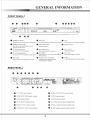
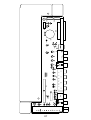
1.2 FRANT PENEL& REAR PENEL.....................................................................................2
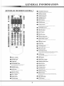
1.3 REMOTE CONTROL............................................................................. .......................3
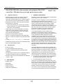
2. BLOCK DIAGRAM
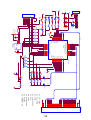
2.1 BLOCK DIAGRAM........................................................................................................4.
2.2 SCHEMATIC DIAGRAM.................................................................................................5
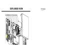
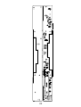
3. EXPLODED VIEW......................................................................6
4. PARTS SPECIFICATIONS
4.1 2A265.....................................................................................................................7-10
4.2 CS9800.................................................................................................................11-18
4.3 DRAM 2M*32(EM638165).......................................................................................19-22
4.4 CS4955.................................................................................................................23-25
4.5 CS4360.................................................................................................................26-30
4.6 CS92288...............................................................................................................31-45
4.7 DRAM 1M*16(VT3617161)......................................................................................46-49
4.8 SAA7114H.............................................................................................................50-57
4.9 CS533...................................................................................................................58-59
4.10 PCF8563.............................................................................................................60-62
4.11 TUNER................................................................................................................... .63
4.12 VFD DRIVER PT6312.................................................................... ......................64-65
4.13 SERVO............................................................................................. .......................66
4.14 HDD INFORMATION.............................................................................................67-68
5. SCHEMATIC DIAGRAM
5.1 POWER SCHEMATIC..................................................................... .......................69-70
5.2 MAIN SCHEMATIC......................................................................... .......................71-79
5.3 AV INPUT /OUTPUT SCHEMATIC.................................................... ...................... 80-87
5.4 VFD DRIVER........................................................................................................ 88-89
6. PARTS LIST
6.1 MAIN BOARD........................................................................................................90-92
6.2 VFD DRIVER BOARD.......................................................................... .......................93
6.3 POWER BOARD....................................................................................................94-95
6.4 AV BOARD.................................................................................................................96
1
2
3
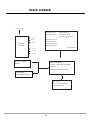
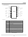
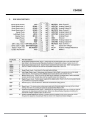
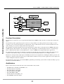
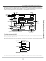
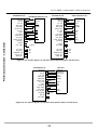
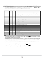
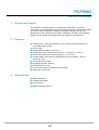
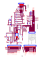
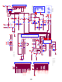
BLOCK DIAGRAM
~110~240V
VIDEO OUT
AUDIO OUT
+12V
+5V
POWER
BOARD
-12V
VIDIO IN PUT
AUDIO IN PUT
TUNER75 IN PUT
S-VIDEO OUT
CB.CR.YOUT
COAXIAL OUT
OPTICAL OUT
AV BOARD
+3.3V
+2.5V
+1.8V
DVD LOADER
DRIVE
MAIN BOARD
MPEG VIDEO DECODER&
MPEG-2
AUDIO/ VIDEO CODER
40GB HDD
40GB HDD DRIVE
PT16312
KEY SCANNING &
VFD DISPLAY
4
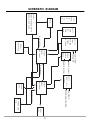
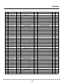
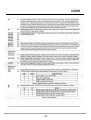
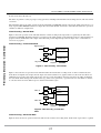
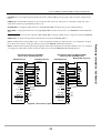
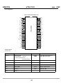
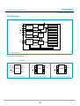
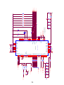
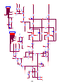
SCHEMATIC DIAGRAM
P-CTL
5VSTB
1.8V
2.5V
VCC
3.3V
CPLD
CS5331
AUDIO
ADC
AUDIO
L.R CH
ATAPI
TO DVD LOADER DRIVE
HDD ATAPI I/O CHAN
SAA7114
VIDEO
DECODER
S-VIDEO
TO-TUNER
Host interface
To front panel
AUDIO R(3CH)
AUDIO L3CH
TO S-VIDEO
TO TUNER
CS4360
AUDIO
DACS
CS92288
MPEG-2
A/V CODEC
DRAM
1M*16 4PCS
CS4955
VIDEO—— D/A
ENCODER
SS9800
MPEG
DECODER
FLASH
16M
S-VIDEO
COMPOSITE VIDEO
To front panel
DRAM
2M*32
TO VFD BOARD
CN104
5
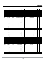
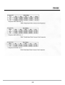
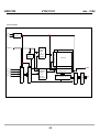
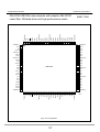
EXPLODED VIEW
15
14
13
12
11
10
9
8
7
6
5
4
3
1
2
22
23
24
18
19
20
21
16
17
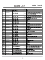
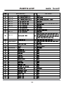
NO.
ITEM NAME
Mirror bar
Left decorative bar
Tray door
Front panel
Left four-key button
Small light conductor
Big light conductor
LED stander
VFD driver board
Chasis
Loader mechanism
DVD loader
Iron stand
Power board
Top cover
Rear panel
AV board
Main board
Hard disc
Copper column
Rubber pad
Open/close button
Right four-key button
Right decorative bar
MATERIAL QUANTITY
pc
ABS
ABS
ABS
ABS
PMMA
PMMA
PS
SECC
PS
SECC
SECC
SECC
RUBBER
ABS
ABS
ABS
6
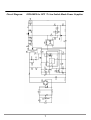
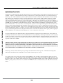
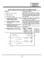
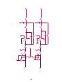
Circuit Diagram:
ICE2AXXX for OFF ¨C Line Switch Mode Power Supplies
7
ICE2AXXX for OFF – Line Switch Mode Power Supplies
Protection Functions
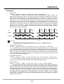
The block diagram displayed in Fig. 4 shows the interal functions of the protection unit. The
comparators C1, C2, C3 and C4 compare the soft-start and feedback-pin voltages. Logic gates
connected to the comparator outputs ensure the combination of the signals and enables the setting of
the “Error-Latch”.
8
ICE2AXXX for OFF – Line Switch Mode Power Supplies
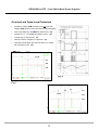
Overload and Open-Loop Protection
•
Feedback voltage (VFB) exceeds 4.8V and soft start
voltage (VSS) is above 5.3V (soft start is completed) (t1)
•
After a 5µs delay the CoolMOS is switched off (t2)
•
Voltage at Vcc – Pin (VCC) decreases to 8.5V (t2)
•
Control logic is switched off (t3)
•
Start-up resistor charges Vcc capacitor (t3)
•
Operation starts again with soft start after Vcc voltage
has exceeded 13.5V (t4)
t1, t2
VCC
VFB
VSS
t1 t2
t3
t4
Fig. 6
Fig. 7
t3
t1, t2
t4
VCC
VFB
VSS
9
ICE2AXXX for OFF – Line Switch Mode Power Supplies
References
[1]
Keith Billings,
Switch Mode Power Supply Handbook
[2]
Ralph E. Tarter,
Solid-State Power Conversion Handbook
[3]
R. D. Middlebrook and Slobodan Cuk,
Advances in Switched-Mode Power Conversion
[4]
Herfurth Michael,
Ansteuerschaltungen für getaktete Stromversorgungen mit Erstellung eines linearisierten
Signalflußplans zur Dimensionierung der Regelung
[5]
Herfurth Michael,
Topologie, Übertragungsverhalten und Dimensionierung häufig eingesetzter
Regelverstärker
[6]
Infineon Technologies, Datasheet,
CoolSET-II
Off – Line SMPS Current Mode Controller with 650V/800V CoolMOSä
ä on Board,
[7]
Robert W. Erickson,
Fundamentals of Power Electronics
10
CS98000
Internet DVD (iDVD) Chip Solution
Features
Description
l Powerful Dual 32-bit RISCs >160MIPS
l Software based on popular RTOS, C/C++
l MPEG video decoder supports DVD, VCD,
Overall the CS98000 Crystal DVD Processor is targeted
as a market specific consumer entertainment processor
empowering new product classes with the inclusion of a
DVD player as a fundamental feature. This integrated
circuit when used with all the other Crystal mixed signal
data converters, DSPs and high quality factory firmware
enables the conception and rapid design of market leading internet age products like:
VCD 3.0, SVCD standards
l Video input with picture-in-picture & zoom
l 8-bit multi-region OSD w/vertical flicker filter
l Universal subpicture unit for DVD and SVCD
l PAL<->NTSC Scaling ~ Transcoding
l Supports SDRAM and FLASH memories
l Powerful 32-bit Audio DSP >80 MIPS
l Decodes: 5.1 channel AC-3, MPEG Stereo
l Plays MP-3 CDs (a MP-3 CD =12 albums)
l Karaoke echo mix and pitch shift
l Optional 3-D Virtual, bass & treble control
l 8-channel dual-zone PCM output
l IEC-60958/61937 Out: AC-3, DTS, MPEG
l Multi-Mode Serial Audio I/O: I2S & AC-Link
l AV Bus or ATAPI interface or DVD/CD/HD
l GPIO support for all common sub-circuits
RISC-1
•
•
•
•
Future Firmware Enhancements:
•
•
•
•
I-Cache
D-Cache
I-Cache
D-Cache
MMU
MAC
MMU
MAC
MPEG Decoder
VLC Parser
IDCT
RAM
Clock Manager
Dataflow Engine
DMA / BitBlit
MoCo
SRAM Buffer
Video Processor
On-Screen Display
External I/Os
Picture-in-Picture
Video/Graphics Display
Preliminary Product Information
Web I/O via AC-Link Input & Built-in Soft Modem
DVD Audio Navigation
MLP Decoder, DTS Decoder, AAC Decoder
MP-3 Encoder, Ripping Controller
ORDERING INFORMATION
CS98000-CQ
0° to 70° C
CS98010-CQ
0° to 70° C
RISC-2
Video Input
Scaler
Filter
DVD A/V Mini-System
Home Media Controller
Combination DVD Player
Car/SUV Entertainment Unit
Remote Input
GPIOs
Memory Controller
32- Bit DSP
SDRAM Control
I-Cache
FLASH Control
X,Y Data
Memory
Subpicture Decode
CPU / MAC
208-pin
128-pin
Scaler
System Controls
Audio I/O
PCM Out
STC
PCM In
Interrupts
XMT958
Registers
SDRAM
A/V Bus
ATAPI-IDE
Local Bus
This document contains information for a new product.
Cirrus Logic reserves the right to modify this product without notice.
11
CS98000
6. PIN DESCRIPTION
Host/Loader
(30)
H_D_[15:0]
H_CS_[3:0]
H_A_[4:0]
H_ALE
H_RD
H_WR
H_CKO
H_RDY
Video In
(12)
VIN_D[7:0]
VIN_HSNC
VIN_VSNC
VIN_CLK
VIN_FLD
CODEC IF
(5)
CDC_DI
CDC_DO
CDC_RST
CDC_CK
CDC_SY
CS98000
XTLCLOCK
RST_N
IR_IN
MFG_TST
GPIO_D[20-0]
GPIO_H[16-14]
GPIO_V10
GPIO_[15-10, 8-7, 4-2, 0]
MISC.
(41)
M_A_[11:0]
M_BS_L
M_D_[31:0]
M_DQM_[3:0]
M_RAS_L
M_CAS_L
M_WE_L
M_AP
M_CKE
M_CKO
NVR_OE_L
NVR_WR_L
Memory IF
(57)
HSYNC
VSYNC
CLK27_O
VDAT_[7:0]
Video out
(11)
AUD_BCK
AUD_LRCK
AUD_DO_[3:0]
SPDIF_O
DAC Out
(7)
AIN_BCK
AIN_LRCK
AIN_DATA
ADC In
(3)
Table 5 lists the conventions used to identify the pin type and direction in the table that follows.
I
Input
IS
Input, with schmitt trigger
ID
Input, with pull down resistor
IU
Input, with pull up resistor
O
Output
O4
Output – 4mA drive
O8
Output – 8mA drive
T4
Tri-State-able Output – 4mA drive
B
Bi-direction
B4
Bi-direction – 4mA drive
B4U
Bi-direction – 4mA drive, with pull-up
B8U
Bi-direction – 8mA drive, with pull-up
B4S
Bi-direction – 4mA drive, with schmitt trigger
B4SU
Bi-direction – 4mA drive, with pull-up and schmitt trigger
Pwr
+2.5V or +3.3V power supply voltage
Gnd
Power supply ground
Name_N
Low active
Name_L
Low active
Table 5. Pin Type legend
12
CS98000
6.1
pins. For some signal pins, a secondary function
and direction are also shown. For pins having more
than one function, the primary function is chosen
when the chip is reset.
Pin Assignments
Table 6 lists the pin number, pin name and pin type
for the 208 pin CS98000 package. The primary
function and pin direction is shown for all signal
Pin
Name
Type
Primary Function
1
VDD_PLL
Pwr
PLL Power 2.5V
Dir
Secondary Function
Dir
2
M_A_11
O8
SDRAM Address[11]
O
ROM/NVRAM Address[11]
O
3
M_A_10
O8
SDRAM Address[10]
O
ROM/NVRAM Address[10]
O
4
GPIO_D18
B4U
5
M_A_9
O8
GenioDVD[18]
B
System Clock PLL Bypass
I
SDRAM Address[9]
O
ROM/NVRAM Address[9]
O
6
M_A_8
O8
SDRAM Address[8]
O
ROM/NVRAM Address8]
O
7
M_A_7
O8
SDRAM Address[7]
O
ROM/NVRAM Address[7]
O
8
GPIO_D16
B4SU
GenioDVD[16]
B
9
M_A_6
O8
SDRAM Address[6]
O
ROM/NVRAM Address[6]
O
10
M_A_5
O8
SDRAM Address[5]
O
ROM/NVRAM Address[5]
O
11
M_A_4
O8
SDRAM Address[4]
O
ROM/NVRAM Address[4]
O
12
GPIO_D17
B4U
GenioDVD[17]
B
13
M_A_3
O8
SDRAM Address[3]
O
ROM/NVRAM Address[3]
O
14
M_A_2
O8
SDRAM Address[2]
O
ROM/NVRAM Address[2]
O
15
M_A_1
O8
SDRAM Address[1]
O
ROM/NVRAM Address[1]
O
16
M_A_0
O8
SDRAM Address[0]
O
ROM/NVRAM Address[0]
O
17
GPIO_D19
B4U
GenioDVD[19]
B
Memory Clock PLL Bypass
I
18
VSS_IO
Gnd
I/O Ground
19
M_CKO
O8
SDRAM Clock
20
VDD_IO
Pwr
I/O Power 3.3V
21
M_BS_L
O8
SDRAM Bank Select
O
22
M_CKE
B8
SDRAM Clock Enable
O
GenioMis(7)
B
23
M_AP
O8
SDRAM Auto Pre-charge
O
24
M_RAS_L
O8
SDRAM Row Strobe
O
25
M_CAS_L
O8
SDRAM Column Strobe
O
26
GPIO_D20
B4U
GenioDVD[20]
B
27
M_WE_L
O8
SDRAM Write Enable
O
28
M_DQM_0
O8
SDRAM DQM[0]
O
29
M_DQM_1
O8
SDRAM DQM[1]
O
30
GPIO_D0
B4U
GenioDVD[0]
B
31
M_DQM_2
O8
SDRAM DQM[2]
O
32
M_DQM_3
O8
SDRAM DQM[3]
O
33
M_D_8
B8U
SDRAM Data[8]
B
ROM/NVRAM Data[8]
B
34
GPIO_D1
B4U
GenioDVD[1]
B
35
VSS_IO
Gnd
I/O Ground
O
Table 6. Pin assignments
13
Note
CS98000
36
VSS_CORE
Gnd
Core Ground
37
M_D_7
B8U
SDRAM Data[7]
38
VDD_IO
Pwr
I/O Power 3.3V
39
GPIO_D2
B4U
GenioDVD[2]
B
40
M_D_9
B8U
SDRAM Data[9]
41
VDD_CORE
Pwr
Core Power 2.5V
42
M_D_6
B8U
SDRAM Data[6]
43
GPIO_D3
B4U
GenioDVD[3]
B
44
M_D_10
B8U
SDRAM Data[10]
45
M_D_5
B8U
46
M_D_11
B8U
47
GPIO_D4
48
M_D_4
49
50
ROM/NVRAM Data[7]
B
B
ROM/NVRAM Data[9]
B
B
ROM/NVRAM Data[6]
B
B
ROM/NVRAM Data[10]
B
SDRAM Data[5]
B
ROM/NVRAM Data[5]
B
SDRAM Data[11]
B
ROM/NVRAM Data[11]
B
B4U
GenioDVD[4]
B
B8U
SDRAM Data[4]
B
ROM/NVRAM Data[4]
B
M_D_12
B8U
SDRAM Data[12]
B
ROM/NVRAM Data[12]
B
GPIO_D5
B4U
GenioDVD[5]
B
51
M_D_3
B8U
SDRAM Data[3]
B
ROM/NVRAM Data[3]
B
52
UNUSED
may leave unconnected
53
UNUSED
may leave unconnected
54
M_D_13
B
ROM/NVRAM Data[13]
B
B8U
B
SDRAM Data[13]
55
M_D_2
B8U
SDRAM Data[2]
B
ROM/NVRAM Data[2]
B
56
M_D_14
B8U
SDRAM Data[14]
B
ROM/NVRAM Data[14]
B
57
GPIO_D6
B4U
GenioDVD[6]
B
58
VSS_IO
Gnd
I/O Ground
59
M_D_1
B8U
SDRAM Data[1]
B
ROM/NVRAM Data[1]
B
60
M_D_15
B8U
SDRAM Data[15]
B
ROM/NVRAM Data[15]
B
61
GPIO_D7
B4U
GenioDVD[7]
I
62
M_D_0
B8U
SDRAM Data[0]
B
ROM/NVRAM Data[0]
B
63
VSS_CORE
Gnd
Core Ground
64
M_D_24
B8U
SDRAM Data[24]
B
ROM/NVRAM Address[20]
O
65
GPIO_D11
B4U
GenioDVD[11]
B
66
VDD_CORE
Pwr
Core Power 2.5V
67
M_D_23
B8U
SDRAM Data[23]
B
ROM/NVRAM Address[19]
O
68
M_D_25
B8U
SDRAM Data[23]
B
ROM/NVRAM Address[21]
O
69
GPIO_D10
B4U
GenioDVD[10]
B
70
M_D_22
B8U
SDRAM Data[22]
B
ROM/NVRAM Address[18]
O
71
M_D_26
B8U
SDRAM Data[26]
B
ROM/NVRAM Address[22]
O
72
M_D_21
B8U
SDRAM Data[21]
B
ROM/NVRAM Address[17]
O
73
GPIO_D9
B4U
GenioDVD[9]
B
74
M_D_27
B8U
SDRAM Data[27]
B
ROM/NVRAM Address[23]
O
75
M_D_20
B8U
SDRAM Data[20]
B
ROM/NVRAM Address[16]
O
76
M_D_28
B8U
SDRAM Data[28]
B
B
Table 6. Pin assignments (Continued)
14
CS98000
77
GPIO_D8
B4U
GenioDVD[8]
B
78
M_D_19
B8U
SDRAM Data[19]
B
79
M_D_29
B8U
SDRAM Data[29]
B
80
M_D_18
B8U
SDRAM Data[18]
81
NV_WE_L
B4U
NVRAM Write Enable
82
VSS_CORE
Gnd
Core Ground
83
M_D_30
B8U
SDRAM Data[30]
84
VDD_CORE
Pwr
Core Power 2.5V
ROM/NVRAM Address[15]
O
B
ROM/NVRAM Address[14]
O
O
GenioMis[8]
B
B
ROM/NVRAM Decode Low
O
85
H_ALE
B4U
Host Address Latch
O
GenioHst[13]
B
86
M_D_17
B8U
SDRAM Data[18]
B
ROM/NVRAM Address[13]
O
87
M_D_31
B8U
SDRAM Data[31]
B
ROM/NVRAM Decode High
O
88
M_D_16
B8U
SDRAM Data[16]
B
ROM/NVRAM Address[12]
O
89
GPIO_H14
B4U
GenioHst[14]
B
90
NV_OE_L
O4
ROM/NVRAM Output
Enable
O
91
VDD_IO
Pwr
I/O Power 3.3V
92
H_RD
B4S
Host Read Strobe
O
DVD Data Strobe
I
1
DVD Data Enable
I
1
93
H_WR
B4
Host Write Strobe
O
94
GPIO_H15
B4U
GenioHst[15]
B
95
H_RDY
B4
Host Ready
I
DVD Data Ready
O
1
96
VSS_IO
Gnd
I/O Ground
GenioHst[10]
B
1
97
H_A_2
B4
Host Address[2]
O
98
GPIO_H16
B4U
GenioHst[16]
B
99
H_A_1
B4
Host Address[1]
O
GenioHst[9]
B
1
100
H_A_0
B4
Host Address[0]
O
GenioHst[8]
B
1
101
H_CS_1
B4
Host Chip Select [1]
O
DVD Error
I
1
102
H_A_4
B4
Host Address[4]
O
GenioHst[12]
B
1
103
VSS_CORE
Gnd
Core Ground
104
VSS_PLL
Gnd
PLL Ground
105
VDD_PLL
Pwr
PLL Power 2.5V
106
H_CS_0
B4
Host Chip Select[0]
O
DVD Start Sector
I
1
107
H_A_3
B4
Host Address[3]
O
GenioHst[11]
B
1
108
VDD_CORE
Pwr
Core Power 2.5V
109
H_D_15
B4
Host Data[15]
B
CD Data
I
1, 2
110
H_D_14
B4
Host Data[14]
B
CD Left Right Clock
I
1, 2
111
H_CS_3
B4
Host Chip Select[3]
O
GenioHst[18]
B
1
112
H_D_13
B4S
Host Data[13]
B
CD Clock
I
1, 2
113
H_D_12
B4
Host Data[12]
B
CD Error
I
1, 2
114
H_D_11
B4
Host Data[11]
B
DVD Control Data In
I
1, 2
115
H_CS_2
B4
Host Chip Select[2]
O
GenioHst[17]
B
1
116
H_D_10
B4
Host Data[10]
B
DVD Control Data Out
O
1, 2
Table 6. Pin assignments (Continued)
15
CS98000
117
H_D_9
B4
Host Data[9]
B
DVD Control Ready
I
1, 2
B
DVD Control Clock
O
1, 2
118
H_D_8
B4
Host Data[8]
119
VSS_IO
Gnd
I/O Ground
120
H_CKO
B4
Host Clock
O
GenioHst[19]
B
1
121
H_D_7
B4
Host Data[7]
B
DVD Data[7]
I
1
122
H_D_6
B4
Host Data[6]
B
DVD Data[6]
I
1
123
H_D_5
B4
Host Data[5]
B
DVD Data[5]
I
1
124
AUD_BCK
B4
Audio Out Bit Clock
O
GenioMis[3]
B
125
H_D_4
B4
Host Data[4]
B
DVD Data[4]
I
1
126
VSS_CORE
Gnd
Core Ground
127
H_D_3
B4
Host Data[3]
B
DVD Data[3]
I
1
128
AUD_LRCK
O4
Audio Out LR Clock
O
129
VDD_CORE
Pwr
Core Power 2.5V
B
DVD Data[2]
I
1
1
130
H_D_2
B4
Host Data[2]
131
VDD_IO
Pwr
I/O Power 3.3V
132
H_D_1
B4
Host Data[1]
B
DVD Data[1]
I
133
AUD_DO_2
B4
Audio Out Data[2]
O
GenioMis[2]
B
DVD Data[0]
I
GenioMis[1]
B
GenioMis[0]
B
134
H_D_0
B4
Host Data[0]
B
135
AUD_DO_0
O4
Audio Out Data[0]
O
136
AUD_DO_1
B4
Audio Out Data[1]
O
137
AIN_BCK
IU
Audio In Bit Clock
I
138
VSS_CORE
Gnd
Core Ground
139
AIN_LRCK
IU
Audio In LR Clock
I
140
AIN_DATA
B4U
Audio In Data
I
141
VDD_CORE
Pwr
Core Power 2.5V
142
CDC_DI
IU
Serial CODEC Data In
143
VSS_IO
Gnd
I/O Ground
144
CDC_DO
T4
Serial CODEC Data Out
O
145
VIN_CLK
IU
Video Input Clock
I
146
CDC_RST
T4
Serial CODEC Reset
O
147
CDC_CK
IU
Serial CODEC Bit Clock
I
148
CDC_SY
B4U
Serial CODEC Sync
B
149
GPIO_V10
B4U
GenioMis[26]
B
150
GPIO_D15
B4U
GenioDvd[15]
151
GPIO_D14
B4U
GenioDvd[14]
152
GPIO_D13
B4SU
GenioDvd[13]
153
VIN_VSNC
B4U
Video Input Vsync
I
GenioMis[25]
B
154
CLK27_O
B4U
Video Output Clock
O
GenioMis[6]
B
155
GPIO_D12
B4U
GenioDvd[12]
156
VDD_PLL
Pwr
PLL Power 2.5V
157
VSS_PLL
Gnd
PLL Ground
I
Table 6. Pin assignments (Continued)
16
1
CS98000
158
VSS_CORE
Gnd
Core Ground
159
HSYNC
B4U
Video Output Hsync
O
GenioMis[4]
B
160
VIN_HSYNC
B4U
Video Input Hsync
I
GenioMis[24]
B
161
VDD_CORE
Pwr
Core Power 2.5V
162
VSYNC
B4U
Video Output Vsync
O
GenioMis[5]
B
163
VDAT_0
O4
Video Output Data[0]
O
164
VIN_D0
B4U
Video Input Data[0]
I
GenioMis[16]
B
165
VDAT_1
O4
Video Output Data[1]
O
166
VDAT_2
O4
Video Output Data[2]
O
167
VDAT_3
O4
Video Output Data[3]
O
168
VIN_D1
B4U
Video Input Data[1]
I
GenioMis[17]
B
169
VDAT_4
O4
Video Output Data[4]
O
170
VDAT_5
O4
Video Output Data[5]
O
171
UNUSED
172
VDAT_6
O4
Video Output Data[6]
O
173
VDAT_7
O4
Video Output Data[7]
O
174
GPIO_0
B4U
General Purpose IO[0]
B
Audio PLL Input Bypass
I
175
VIN_D2
B4U
Video Input Data[2]
I
GenioMis[18]
B
176
VSS_CORE
Gnd
Core Ground
177
AUD_DO_3
B4U
Audio Out Data[3]
O
General Purpose IO[1]
B
178
VDD_CORE
Pwr
Core Power 2.5V
179
VIN_D3
B4U
Video Input Data[3]
I
GenioMis[19]
B
180
VDD_IO
Pwr
I/O Power 3.3V
181
GPIO_2
B4U
General Purpose IO[2]
182
VSS_IO
Gnd
I/O Ground
183
GPIO_3
B4U
General Purpose IO[3]
B
184
VIN_D4
B4U
Video Input Data[4]
I
GenioMis[20]
B
185
GPIO_4
B4U
General Purpose IO[4]
B
186
SCL
may leave unconnected
B4U
I2C
2
B
Clock
B
General Purpose IO[5]
B
General Purpose IO[6]
B
GenioMis[21]
B
General Purpose IO[9]
B
GenioMis[22]
B
GenioMis[23]
B
187
SDA
B4U
I C Data
B
188
GPIO_7
B4U
General Purpose IO[7]
B
189
VIN_D5
B4U
Video Input Data[5]
I
190
GPIO_8
B4U
General Purpose IO[8]
B
191
AUD_XCLK
B4U
Audio 256x/384x Clock
B
192
GPIO_10
B4U
General Purpose IO[10]
B
193
VIN_D6
B4U
Video Input Data[6]
I
194
GPIO_11
B4U
General Purpose IO[11]
B
195
GPIO_12
B4U
General Purpose IO[12]
B
196
GPIO_13
B4U
General Purpose IO[13]
B
197
GPIO_14
B4U
General Purpose IO[14]
B
198
VIN_D7
B4U
Video Input Data[7]
I
Table 6. Pin assignments (Continued)
17
CS98000
158
VSS_CORE
Gnd
Core Ground
159
HSYNC
B4U
Video Output Hsync
O
GenioMis[4]
B
160
VIN_HSYNC
B4U
Video Input Hsync
I
GenioMis[24]
B
161
VDD_CORE
Pwr
Core Power 2.5V
162
VSYNC
B4U
Video Output Vsync
O
GenioMis[5]
B
163
VDAT_0
O4
Video Output Data[0]
O
164
VIN_D0
B4U
Video Input Data[0]
I
GenioMis[16]
B
165
VDAT_1
O4
Video Output Data[1]
O
166
VDAT_2
O4
Video Output Data[2]
O
167
VDAT_3
O4
Video Output Data[3]
O
168
VIN_D1
B4U
Video Input Data[1]
I
GenioMis[17]
B
169
VDAT_4
O4
Video Output Data[4]
O
170
VDAT_5
O4
Video Output Data[5]
O
171
UNUSED
172
VDAT_6
O4
Video Output Data[6]
O
173
VDAT_7
O4
Video Output Data[7]
O
174
GPIO_0
B4U
General Purpose IO[0]
B
Audio PLL Input Bypass
I
175
VIN_D2
B4U
Video Input Data[2]
I
GenioMis[18]
B
176
VSS_CORE
Gnd
Core Ground
177
AUD_DO_3
B4U
Audio Out Data[3]
O
General Purpose IO[1]
B
178
VDD_CORE
Pwr
Core Power 2.5V
179
VIN_D3
B4U
Video Input Data[3]
I
GenioMis[19]
B
180
VDD_IO
Pwr
I/O Power 3.3V
181
GPIO_2
B4U
General Purpose IO[2]
182
VSS_IO
Gnd
I/O Ground
183
GPIO_3
B4U
General Purpose IO[3]
184
VIN_D4
B4U
Video Input Data[4]
I
GenioMis[20]
B
185
GPIO_4
B4U
General Purpose IO[4]
B
186
SCL
B4U
I2C Clock
B
General Purpose IO[5]
B
General Purpose IO[6]
B
GenioMis[21]
B
General Purpose IO[9]
B
GenioMis[22]
B
GenioMis[23]
B
may leave unconnected
2
B
B
B4U
I C Data
B
GPIO_7
B4U
General Purpose IO[7]
B
VIN_D5
B4U
Video Input Data[5]
I
190
GPIO_8
B4U
General Purpose IO[8]
B
191
AUD_XCLK
B4U
Audio 256x/384x Clock
B
192
GPIO_10
B4U
General Purpose IO[10]
B
193
VIN_D6
B4U
Video Input Data[6]
I
194
GPIO_11
B4U
General Purpose IO[11]
B
195
GPIO_12
B4U
General Purpose IO[12]
B
196
GPIO_13
B4U
General Purpose IO[13]
B
197
GPIO_14
B4U
General Purpose IO[14]
B
198
VIN_D7
B4U
Video Input Data[7]
I
187
SDA
188
189
Table 6. Pin assignments (Continued)
18
EM638165
Pin Descriptions
Table 1. Pin Details of EM638165
Symbol
Type
Description
CLK
Input
Clock: CLK is driven by the system clock. All SDRAM input signals are
sampled on the positive edge of CLK. CLK also increments the internal burst
counter and controls the output registers.
CKE
Input
Clock Enable: CKE activates(HIGH) and deactivates(LOW) the CLK signal. If
CKE goes low synchronously with clock(set-up and hold time same as other
inputs), the internal clock is suspended from the next clock cycle and the state
of output and burst address is frozen as long as the CKE remains low. When all
banks are in the idle state, deactivating the clock controls the entry to the Power
Down and Self Refresh modes. CKE is synchronous except after the device
enters Power Down and Self Refresh modes, where CKE becomes
asynchronous until exiting the same mode. The input buffers, including CLK,
are disabled during Power Down and Self Refresh modes, providing low
standby power.
BA0,BA1
Input
Bank Select: BA0,BA1 input select the bank for operation.
BA1
BA0
Select Bank
0
0
BANK #A
0
1
BANK #B
1
0
BANK #C
1
1
BANK #D
A0-A11
Input
Address Inputs: A0-A11 are sampled during the BankActivate command (row
address A0-A11) and Read/Write command (column address A0-A7 with A10
defining Auto Precharge) to select one location out of the 2M available in the
respective bank. During a Precharge command, A10 is sampled to determine if
all banks are to be precharged (A10 = HIGH). The address inputs also provide
the op-code during a Mode Register Set command.
CS#
Input
Chip Select: CS# enables (sampled LOW) and disables (sampled HIGH) the
command decoder. All commands are masked when CS# is sampled HIGH.
CS# provides for external bank selection on systems with multiple banks. It is
considered part of the command code.
RAS#
Input
Row Address Strobe: The RAS# signal defines the operation commands in
conjunction with the CAS# and WE# signals and is latched at the positive edges
of CLK. When RAS# and CS# are asserted "LOW" and CAS# is asserted
"HIGH," either the BankActivate command or the Precharge command is
selected by the WE# signal. When the WE# is asserted "HIGH," the
BankActivate command is selected and the bank designated by BS is turned on
to the active state. When the WE# is asserted "LOW," the Precharge command
is selected and the bank designated by BS is switched to the idle state after the
precharge operation.
CAS#
Input
Column Address Strobe: The CAS# signal defines the operation commands in
conjunction with the RAS# and WE# signals and is latched at the positive edges
of CLK. When RAS# is held "HIGH" and CS# is asserted "LOW," the column
access is started by asserting CAS# "LOW." Then, the Read or Write command
is selected by asserting WE# "LOW" or "HIGH."
19
EM638165
Pin Descriptions
Table 1. Pin Details of EM638165
Symbol
Type
Description
CLK
Input
Clock: CLK is driven by the system clock. All SDRAM input signals are
sampled on the positive edge of CLK. CLK also increments the internal burst
counter and controls the output registers.
CKE
Input
Clock Enable: CKE activates(HIGH) and deactivates(LOW) the CLK signal. If
CKE goes low synchronously with clock(set-up and hold time same as other
inputs), the internal clock is suspended from the next clock cycle and the state
of output and burst address is frozen as long as the CKE remains low. When all
banks are in the idle state, deactivating the clock controls the entry to the Power
Down and Self Refresh modes. CKE is synchronous except after the device
enters Power Down and Self Refresh modes, where CKE becomes
asynchronous until exiting the same mode. The input buffers, including CLK,
are disabled during Power Down and Self Refresh modes, providing low
standby power.
BA0,BA1
Input
Bank Select: BA0,BA1 input select the bank for operation.
BA1
BA0
Select Bank
0
0
BANK #A
0
1
BANK #B
1
0
BANK #C
1
1
BANK #D
A0-A11
Input
Address Inputs: A0-A11 are sampled during the BankActivate command (row
address A0-A11) and Read/Write command (column address A0-A7 with A10
defining Auto Precharge) to select one location out of the 2M available in the
respective bank. During a Precharge command, A10 is sampled to determine if
all banks are to be precharged (A10 = HIGH). The address inputs also provide
the op-code during a Mode Register Set command.
CS#
Input
Chip Select: CS# enables (sampled LOW) and disables (sampled HIGH) the
command decoder. All commands are masked when CS# is sampled HIGH.
CS# provides for external bank selection on systems with multiple banks. It is
considered part of the command code.
RAS#
Input
Row Address Strobe: The RAS# signal defines the operation commands in
conjunction with the CAS# and WE# signals and is latched at the positive edges
of CLK. When RAS# and CS# are asserted "LOW" and CAS# is asserted
"HIGH," either the BankActivate command or the Precharge command is
selected by the WE# signal. When the WE# is asserted "HIGH," the
BankActivate command is selected and the bank designated by BS is turned on
to the active state. When the WE# is asserted "LOW," the Precharge command
is selected and the bank designated by BS is switched to the idle state after the
precharge operation.
CAS#
Input
Column Address Strobe: The CAS# signal defines the operation commands in
conjunction with the RAS# and WE# signals and is latched at the positive edges
of CLK. When RAS# is held "HIGH" and CS# is asserted "LOW," the column
access is started by asserting CAS# "LOW." Then, the Read or Write command
is selected by asserting WE# "LOW" or "HIGH."
20
EM638165
Operation Mode
Fully synchronous operations are performed to latch the commands at the positive edges of CLK.
Table 2 shows the truth table for the operation commands.
Table 2. Truth Table (Note (1), (2) )
Command
State
CKEn-1 CKEn DQM BA0,1 A10 A0-9,11 CS# RAS# CAS# WE#
Idle(3)
H
X
X
V
BankPrecharge
Any
H
X
X
V
L
PrechargeAll
Any
H
X
X
X
Write
Active(3)
H
X
X
Write and AutoPrecharge
Active(3)
H
X
X
Read
Active(3)
H
X
X
V
L
Read and Autoprecharge
Active(3)
H
X
X
V
H
Mode Register Set
Idle
H
X
X
No-Operation
Any
H
X
X
X
X
Active(4)
H
X
X
X
Device Deselect
Any
H
X
X
AutoRefresh
Idle
H
H
SelfRefresh Entry
Idle
H
Idle
L
BankActivate
Burst Stop
SelfRefresh Exit
Row address
L
L
H
H
X
L
L
H
L
H
X
L
L
H
L
V
L
L
H
L
L
V
H
Column
address
(A0 ~ A7)
L
H
L
L
Column
address
(A0 ~ A7)
L
H
L
H
L
H
L
H
L
L
L
L
X
L
H
H
H
X
X
L
H
H
L
X
X
X
H
X
X
X
X
X
X
X
L
L
L
H
L
X
X
X
X
L
L
L
H
H
X
X
X
X
H
X
X
X
L
H
H
H
OP code
(SelfRefresh)
Clock Suspend Mode Entry
Active
H
L
X
X
X
X
X
X
X
X
Power Down Mode Entry
Any(5)
H
L
X
X
X
X
H
X
X
X
L
H
H
H
Clock Suspend Mode Exit
Power Down Mode Exit
Active
L
H
X
X
X
X
X
X
X
X
Any
L
H
X
X
X
X
H
X
X
X
L
H
H
H
(PowerDown)
Data Write/Output Enable
Active
H
X
L
X
X
X
X
X
X
X
Data Mask/Output Disable
Active
H
X
H
X
X
X
X
X
X
X
Note: 1. V=Valid X=Don't Care L=Low level H=High level
2. CKEn signal is input level when commands are provided.
CKEn-1 signal is input level one clock cycle before the commands are provided.
3. These are states of bank designated by BS signal.
4. Device state is 1, 2, 4, 8, and full page burst operation.
5. Power Down Mode can not enter in the burst operation.
When this command is asserted in the burst cycle, device state is clock suspend mode.
21
EM638165
Commands
1
BankActivate
(RAS# = "L", CAS# = "H", WE# = "H", BAs = Bank, A0-A11 = Row Address)
The BankActivate command activates the idle bank designated by the BA0,1 signals. By
latching the row address on A0 to A11 at the time of this command, the selected row access is
initiated. The read or write operation in the same bank can occur after a time delay of tRCD(min.)
from the time of bank activation. A subsequent BankActivate command to a different row in the
same bank can only be issued after the previous active row has been precharged (refer to the
following figure). The minimum time interval between successive BankActivate commands to the
same bank is defined by tRC(min.). The SDRAM has four internal banks on the same chip and
shares part of the internal circuitry to reduce chip area; therefore it restricts the back-to-back
activation of the four banks. tRRD(min.) specifies the minimum time required between activating
different banks. After this command is used, the Write command and the Block Write command
perform the no mask write operation.
T0
T1
T2
T3
Tn+3
CLK
Tn+4
Tn+5
Tn+6
..............
ADDRESS
Bank A
Row Addr.
Bank A
Col Addr.
..............
Bank B
Row Addr.
R/W A with
AutoPrecharge
..............
Bank B
Activate
RAS# - RAS# delay time (tRRD)
RAS# - CAS# delay (tRCD)
COM MAND
Bank A
Activate
NOP
NOP
Bank A
Row Addr.
NOP
NOP
Bank A
Activate
RAS# Cycle time (tRC)
AutoPrecharge
Begin
: "H" or "L"
BankActivate Command Cycle (Burst Length = n, CAS# Latency = 3)
2
BankPrecharge command
(RAS# = "L", CAS# = "H", WE# = "L", BAs = Bank, A10 = "L", A0-A9 and A11 = Don't care)
The BankPrecharge command precharges the bank disignated by BA signal. The precharged
bank is switched from the active state to the idle state. This command can be asserted anytime after
tRAS(min.) is satisfied from the BankActivate command in the desired bank. The maximum time any
bank can be active is specified by tRAS(max.). Therefore, the precharge function must be performed
in any active bank within tRAS(max.). At the end of precharge, the precharged bank is still in the idle
state and is ready to be activated again.
3
PrechargeAll command
(RAS# = "L", CAS# = "H", WE# = "L", BAs = Don’t care, A10 = "H", A0 -A9 and A11 = Don't care)
The PrechargeAll command precharges all banks simultaneously and can be issued even if all
banks are not in the active state. All banks are then switched to the idle state.
4
Read command
(RAS# = "H", CAS# = "L", WE# = "H", BAs = Bank, A10 = "L", A0-A7 = Column Address)
The Read command is used to read a burst of data on consecutive clock cycles from an active
row in an active bank. The bank must be active for at least tRCD(min.) before the Read command is
issued. During read bursts, the valid data-out element from the starting column address will be
available following the CAS# latency after the issue of the Read command. Each subsequent dataout element will be valid by the next positive clock edge (refer to the following figure). The DQs go
into high-impedance at the end of the burst unless other command is initiated. The burst length,
burst sequence, and CAS# latency are determined by the mode register, which is already
programmed. A full-page burst will continue until terminated (at the end of the page it will wrap to
column 0 and continue).
22
23
24
25
26
27
28
29
30
CS92288 MPEG-2 AUDIO/VIDEO CODEC DATA BOOK
Preliminary Information - Confidential
IMPORTANT NOTICE
"Preliminary" product information describes products that are in production, but for which full characterization data is not yet
available. "Advance" product information describes products that are in development and subject to development changes.
Cirrus Logic, Inc. and its subsidiaries ("Cirrus") believe that the information contained in this document is accurate and reliable. However, the information is subject to change without notice and is provided "AS IS" without warranty of any kind
(express or implied). Customers are advised to obtain the latest version of relevant information to verify, before placing
orders, that information being relied on is current and complete. All products are sold subject to the terms and conditions of
sale supplied at the time of order acknowledgment, including those pertaining to warranty, patent infringement, and limitation
of liability. No responsibility is assumed by Cirrus for the use of this information, including use of this information as the
basis for manufacture or sale of any items, or for infringement of patents or other rights of third parties. This document is the
property of Cirrus and by furnishing this information, Cirrus grants no license, express or implied under any patents, mask
work rights, copyrights, trademarks, trade secrets or other intellectual property rights. Cirrus owns the copyrights of the information contained herein and gives consent for copies to be made of the information only for use within your organization with
respect to Cirrus integrated circuits or other parts of Cirrus. This consent does not extend to other copying such as copying for
general distribution, advertising or promotional purposes, or for creating any work for resale.
An export permit needs to be obtained from the competent authorities of the Japanese Government if any of the products or
technologies described in this material and controlled under the "Foreign Exchange and Foreign Trade Law" is to be exported
or taken out of Japan. An export license and/or quota needs to be obtained from the competent authorities of the Chinese Government if any of the products or technologies described in this material is subject to the PRC Foreign Trade Law and is to be
exported or taken out of the PRC.
CERTAIN APPLICATIONS USING SEMICONDUCTOR PRODUCTS MAY INVOLVE POTENTIAL RISKS OF DEATH,
PERSONAL INJURY, OR SEVERE PROPERTY OR ENVIRONMENTAL DAMAGE ("CRITICAL APPLICATIONS").
CIRRUS PRODUCTS ARE NOT DESIGNED, AUTHORIZED, ORWARRANTED TO BE SUITABLE FOR USE IN LIFESUPPORT DEVICES OR SYSTEMS OR OTHER CRITICAL APPLICATIONS. INCLUSION OF CIRRUS PRODUCTS IN
SUCH APPLICATIONS IS UNDERSTOOD TO BE FULLY AT THE CUSTOMER'S RISK.
Cirrus Logic, Cirrus, and the Cirrus Logic logo designs are trademarks of Cirrus Logic, Inc. All other brand and product
names in this document may be trademarks or service marks of their respective owners.
Use of this product in any manner that complies with the MPEG-2 video standard as defined in ISO documents IS 13818-1
(including annexes C, D, F, J, and K), IS 13818-2 (including annexes A, B, C, and D, but excluding scalable extensions), and
IS 13818-4 (only as it is needed to clarify IS 13818-2) is expressly prohibited without a license under applicable patents in the
MPEG-2 patent portfolio, which license is available from MPEG LA, L.L.C. 250 Steele Street, Suite 300, Denver, Colorado
80296.
31
CS92288 MPEG-2 AUDIO/VIDEO CODEC DATA BOOK
Overview
The CS92288 is a real time MPEG-2 audio/video encoder and decoder (CODEC), with system multiplexor/demultiplexor and
on-screen display (OSD). For video coding, the CS92288 fully complies with the ISO/IEC 13818 Main Level @ Main Profile
(ML@MP) or with the ISO/IEC 11172 (MPEG-1) formats. For audio encoding, the CS92288 supports a variety of audio formats, including MPEG-1 or MPEG-2 audio (all Layers) and Dolby Digital (AC-3).
In encode mode, the CS92288 accepts digital video in ITU-R BT.601 (CCIR-601) or ITU-R BT.656 (CCIR-656) formats, and
digital audio in LPCM format. The input video is filtered and then encoded to produce a compressed bitstream in either
MPEG-1 or MPEG-2 ML@MP syntax. The audio is compressed in either MPEG or Dolby Digital formats. The compressed
video and audio streams are multiplexed to produce an MPEG-compliant program bit stream.
In decode mode, the CS92288 accepts an MPEG program bit stream or audio and video elementary streams and produces ITUR BT.601 or BT.656 video and LPCM audio outputs.
For the evaluation of the CS92288, Cirrus Logic provides a PC-based Evaluation Board, window drivers, and application software. In addition, Cirrus Logic offers a complete reference design for a stand-alone MPEG-based video recorder/player. This
design allows designers and manufacturers a quick entry to the digital recording markets.
Features
•
•
•
•
•
•
•
•
•
•
•
•
•
Single Chip Real Time MPEG-2 Audio/Video CODEC with system Mux/Demux and On-screen Display (OSD)
Supports MPEG-1 audio/video encoding and decoding
Supports Dolby Digital audio encoding and decoding
Programmable system mux/demux supports DVD, VCD, and SVCD encoding and decoding
8-bit OSD support (2-b text, 2-b to 8-b graphics)
Support for Constant Bit Rate (CBR) and one-pass Variable Bit Rate (VBR)
– IPB-pictures, CBR (average), VBR (max) up to 15Mbps.
– I-pictures only to 30Mbps
Proprietary High Performance Motion Estimation
Low external SDRAM memory:
– 8 Mbytes for D1, 2B picture format
Supports Multiple Resolutions & Scan Rates
– NTSC: (720, 704, 640, 544, 480, 352) x 480 or 352 x 240 (CIF), and 176x112 (QCIF) at 30 or 29.97 Hz
– PAL: (720, 704, 640, 544, 480, 352) x 576 or 352 x 288 (CIF), and 176x144 (QCIF) at 25 Hz
Integrated video pre and post processor
108 MHz operating frequency with separate 27 MHz input video clock
Video Preprocessor
– Accepts ITU-R BT.601 4:2:2 and D1 input formats
– 4:2:2 to 4:2:0 Conversion
– Built-in, programmable, pre-processing filters
– Half Horizontal Resolution (HHR), SIF decimation filtering, or Two-Thirds Horizontal resolution filtering
– Temporal filtering
– Automatic inverse telecine
– Sync Extraction
Video Encoder
– Real Time Encoding of MPEG-2 Main Level/Main Profile digital video
• ISO/IEC 13818-2 compliant
• SP@ML, MP@LL, MP@ML
• Video Streams up to 13.5Mpels/s (16-bit) and 27Mpel/s (8-bit)
– Real Time Encoding of MPEG-1
– Support for Full D1, 2/3 D1, 1/2 D1, CIF, and QCIF
32
Preliminary Information - Confidential
The CS92288 is designed to provide a high degree of integration and ease of system design. It makes an ideal solution for a
variety of MPEG-based audio/visual applications, such as PC-based content creation, VCD and DVD-RAM players/recorders,
set-top boxes, and time-shift recording. For example, a single CS92288 is adequate for a complete Super VCD (SVCD) player/
recorder.
Preliminary Information - Confidential
CS92288 MPEG-2 AUDIO/VIDEO CODEC DATA BOOK
– Constant Bit Rate Support: up to 15Mbps (IPB frames) and 30Mbps (I frame only)
– Variable Bit Rate Support:
• Real-time one-pass rate control
• User-selectable average bitrate
– Proprietary High Performance Motion Estimation Engine
• Half-pel accuracy
• Horizontal Search Ranges: ±63.5, ±31.5, ±15.5, ±7.5 Pel/Frame
• Vertical Search Range: ±31.5, ±15.5, ±7.5 Pel/Frame
– Guaranteed to operate at 30 frames/second
– Field-based or Frame-based DCT
– Field, 16x8, and frame-mode prediction
– Programmable encoding parameters
• I and P-picture interval
• quantization matrices
• Encoding time
• Average bitrate, upper and lower bitrate bounds
• Active Picture Area Selection
• Video Decoder
– Decodes ML@MP MPEG-2 video and MPEG-1 video
– Support Full D1, 2/3 D1, 1/2 D1, CIF, and QCIF
– Variable Length Decoder
• Video stream syntax parsing and decoding
• Error detection and handling
– Motion Prediction
• Supports frame, field, 16 x 8 and dual prime motion compensation modes
• Performs half-pel interpolation and bi-directional interpolation
– Error detection, handling and mitigation
• Video Postprocessor
– Filters for interpolation to ITU-R BT.601 and BT.656 format
– Display Management
– Automatic repetition of dropped field for 3:2 Pulldown (Telecine)
– Horizontal and vertical scaling
– Master mode D1/VMI output
– Slave mode CCIR output
– Letter-box, NTSC to PAL format conversion
– OSD/OGD; 2-bit text, 2-,4-, or 8-bit graphics
• Audio Processor
– Programmable, 24-bit, digital signal processor
– Input/Output sampling rates: 32, 44.1, 48, or 96 kHz
– Data resolution up to 24 bits/sample
– Two channel audio encoding or decoding in either MPEG (all Layers) or Dolby Digital (AC-3)
– 5.1 channels audio decoding (downmixed to two channels)
– Additional audio encoding/decoding algorithms can be supported via firmware upgrades
• System Processor
– System Multiplexor/Demultiplexor
– Based on powerful embedded ARC core
– Programmable, supports DVD, VCD, SVCD, encoding and decoding
– Supports Transport, Program, and Elementary streams
– Trick Play; fast and slow play forward, fast play backward
• System Interfaces
– 16-bit bus that supports Intel and Motorola interfaces
– 8-bit interface supports the Philips Trimedia TM1300 and other 8-bit microcontrollers with either separate or multiplexed
address and data buses.
– Gluless interface to Philips 7146 PCI bridge
– Direct interface to NTSC/PAL industry standard NTSC/PAL video encoders/decoders (Philips, Harris)
33
CS92288 MPEG-2 AUDIO/VIDEO CODEC DATA BOOK
– Glueless interface to industry standard SDRAM(s)
– Glueless interface to Data Flash and EPROM memories
– 8051 Protocol interface
– I2S
– General Purposed I/O
– Glueless interface to USB controllers
– Programmable clock output for audio A/D and D/A converters.
• Technology
– 0.18um CMOS technology
– 272-pin PBGA package
– 3.3 and 1.8 Volts power supplies
– 5V I/O tolerance
– Internal pull-ups for SDRAM and HIU data buses
– 1 W typical average power consumption at 108 MHz
Part Number
Package
Operating Temp Range
CS92288
272L-BGA
0o ~ +70o
Application Information
Figure 1shows a digital audio/video deck using the CS92288, a host microcontroller, a CD-R/W drive, and supporting commodity devices. A drive interface is supported by the controller CPU to transfer data between the CS92288 and the CD-R/W
drive. The functionality of the CS92288 can be controlled either from the host microcontroller or from an optional Firmware
EPROM. The OSD EPROM is also optional
Encoding
Analog video is demodulated and passed to the CS92288. The setup and control for the NTSC/PAL video decoder are handled
by an external I2C interface master. Input video can be overlayed with on-screen graphics and be passed back to the NTSC/
PAL video encoder for video output loopback.
Analog audio is digitized by the A/D converter, and LPCM data is transfered to the CS92288 via the I2S interface. Audio loopback is provided by a separate I2S interface to the output audio D/A of the system. The CS92288 utilizes the SDRAM to process
the input audio and video, producing an MPEG-compliant output to the Host CPU. The Host CPU directs the writing of the
data to the media.
Decoding
The compressed audio and video data is read off the media device. The CS92288 demultiplexes and decompresses the audio
and video data and transfers digital video to the NTSC/PAL video encoder and digital LPCM audio to the audio D/A converter.
Furthermore, the output video data can be mixed with OSD or OGT (On-screen Graphics and Text) data before the final output. The NTSC/PAL video encoder is configured by an external I 2C master. The audio D/A interfaces with the CS92288
using the I2S bus and associated interface circuitry.
34
Preliminary Information - Confidential
Ordering Information
CS92288 MPEG-2 AUDIO/VIDEO CODEC DATA BOOK
I2C
Video In
YC/CV
NTSC/PAL
Decoder
I2C
Video Out
YC/CV
NTSC/PAL
Encoder
A/D
Audio In
Preliminary Information - Confidential
Audio Out
Optional Firmware
EPROM or Flash
D/A
Video In
Video Out
CS92288
SDRAM
MPEG-2 A/V
Controller
CODEC
64-bit
8MB
SDRAM
Audio I/O
I2S
Host Interface
Front
Panel
Host CPU
Drive
Interface
CD-R/W
Figure 1: System diagram of an CS92288-based digital A/V Recorder/Player
Functional Descriptions
The CS92288 is organized as a process pipeline that implements the MPEG-2 audio and video encoding and decoding algorithms.
The CS92288 provides application program control over a large number of encoding parameters. For example, for video
encoding one can control such parameters as I, P, B-picture cadence, GOP structure, bit rates, and decoder buffer sizes. For
audio encoding, one can select coding format and average bit rate.
The algorithmic and architectural innovations of the CS92288 allow a unique degree of integration for the MPEG audio/video
CODEC function. The CS92288 is also designed to provide a high degree of system integration and ease of system design.
These combined benefits make it an ideal platform for a variety of MPEG-2-based digital audio/video applications
For communication applications, the CS92288 can match the output bit rate to the channel rate. This feature allows the host
controller to make bit rate changes as needed to demonstrate better bandwidth utilization across multiple channels.
Internal rate control provides a high degree of flexibility in relation to the output bit rate, including the ability to generate variable bit rate compressed video stream in one pass. This makes it suitable for storage sensitive applications such as digital camcorders and digital versatile discs (DVDs).
The CS92288 also has features geared toward MPEG-2 publishing and authoring systems. These include the ability to specify
the initial decoder buffer fullness.
Architecture
Figure 2 shows the major functional units of the CS92288.These units include:
•
•
•
•
•
•
•
The RISC microcontroller (an ARC RISC core)
The Video Interface Unit (VIO)
The Audio Interface Unit (AIU)
The Video Engine Unit (VEU)
The Audio Engine (DSP)
The Host Interface Unit (HIU), and
The SDRAM Control Unit (DCU)
35
CS92288 MPEG-2 AUDIO/VIDEO CODEC DATA BOOK
All blocks inter-communicate with two major data buses: a 64-bit wide data bus (D-Bus) and a 16-bit wide register bus (RBus). The PLL block is used to multiply (4X) the SYSCLK frequency to provide for all internal blocks and external memory
clocking. A separate PLL is used to provide an output clock to external audio A/D and D/A converters.
+1.8V
+3.3V
SYSCLK
CLK27_DEM
CLK27_MOD
Video Engine
Unit (VEU)
(27 MHz)
PLL
R-BUS
Video In
D-BUS
RISC microcontroller (ARC)
Video Out
Audio In
Audio
Interface
Unit (AIU)
Audio
PLL
Audio Out
SDRAM Control
Unit (DCU)
SDRAM
Memory
(108 MHz)
Host
Interface
Unit (HIU)
Audio
Engine Unit
(DSP)
AM_SCLK
Bitstream/Command
Host Interface
Figure 2: CS92288 Chip Architecture
The Video Interface Unit (VIO)
Figure 3 shows a block diagram of the VIO. It includes the Video Input Unit (VIU), the Video Output Unit (VOU), the Video
Processing Unit (VPU), and the OSD Unit.
The VIU selects the input video active area and performs chroma conversion, inverse telecine, spatial and/or temporal prefilter-
Digital Video In
Video Input
Unit (VIU)
601/656
D-Bus
Video Output
Unit (VOU)
Digital Video Out
OSD
601/656
Video Processing
Unit (VPU)
Figure 3: Block diagram of the Video
Interface Unit
ing, and data arrangement to facilitate the subsequent encoding processes. It preprocesses the input data so that encoding can
36
Preliminary Information - Confidential
Video
Interface
Unit (VIO)
CS92288 MPEG-2 AUDIO/VIDEO CODEC DATA BOOK
be done in the most efficient way.
The VOU can perform a variety of postprocessing operations, including horizontal and vertical scaling, telecine, and video format
conversion.
The OSD block mixes text and/or graphics from the OSD buffer (in SDRAM) with the output of the VOU and generates a correctly sequenced ITU-R BT.601 or 656 4:2:2 output video stream. The flexible architecture of the VIO unit allows it to operate in
a number of different configurations.
Video Encoding - Normal Mode
Figure 4 shows the operation of the VIO unit under the normal encoding mode. Input video is captured by the VIU and is
transferred to SDRAM. The buffered input is passed first to the VOU and then to the OSD unit, where it is mixed with text or
graphics from the OSD buffers. The output of the OSD unit provides digital loopback of the input video, overlaid with onscreen text or graphics.
Preliminary Information - Confidential
Video Encoding - Intermediate Mode
Digital Video In
Input/Encoding
Video Buffers
VIU
VOU
OSD Buffers
OSD
Dig. Video Out
Text/
Graphics
SDRAM
Figure 4: Video Encoding - Normal Mode
Figure 5 shows the flow of operations in the VIO unit under the intermediate encoding mode. As in the normal mode, this
mode allows for digital video loopback of the input video with overlaid text or graphics. However, this mode also allows for
additional preprocessing of the input video by the video processing unit (VPU). Among its functions, the VPU can initialize
the video frame buffer with specific YCbCr values (e.g., blue screen generation), copy data from one video buffer to another,
or scale data from one frame-buffer region to another frame-buffer region.
Encoding Video
Buffers
VPU
Video In
Input Video
Buffers
VIU
VOU
Video Out
OSD Buffers
OSD
Text/
Graphics
SDRAM
Figure 5: Video Encoding - Intermediate
Mode
Video Encoding - Advanced Mode
Figure 6 shows the flow of operations when the VIO is used in advanced encoding mode. In this mode, input video is captured
37
CS92288 MPEG-2 AUDIO/VIDEO CODEC DATA BOOK
directly by the OSD unit, where it can be mixed with OSD data. The output of the OSD unit is passed back to the VIU and then
to SDRAM for video encoding. As in the previous mode, additional preprocessing of the video data by the VPU may also be
enabled.
Encoding Video
Buffers
VPU
Input Video
Buffers
VIU
Video Out
VOU
Video In
OSD Buffers
Text/
Graphics
SDRAM
Figure 6: Video Encoding - Advanced Mode
Video Decoding
Figure 7 shows the flow of data in the VIO unit during video decoding. At minimum, decoded video data are transferred from
the SDRAM to the VOU for chroma upconversion and other postprocessing. The output of the VOU is passed to the OSD unit
where it can be mixed with text or graphics before it is transferred to the video output. Optionally, the VPU may also be
enabled to process the decoded data before they are being transferred to the VOU.
.
VPU
Decoded Video
Buffers
VIU
Display Video
Buffers
VOU
Video Out
OSD Buffers
OSD
Text/
Graphics
SDRAM
Figure 7: Video Decoding
The Audio Interface Unit (AIU)
The audio interface unit provides the interface between the CS92288 and external audio devices. Audio samples are transferred in and out of the CS92288 using I2S signaling. The CS92288 also provides a user-configurable output clock for external
audio A/D and D/As.
38
Preliminary Information - Confidential
OSD
CS92288 MPEG-2 AUDIO/VIDEO CODEC DATA BOOK
The RISC Microcontroller
This is an embedded, programmable,32-bit ARC RISC processor. It performs multiplexing and demultiplexing of MPEG program streams and acts as a central sequencer. Its microcode can be downloaded either from an external host, from external data
Flash, or from an external EEPROM, through the Host Interface Unit.
The Video Engine Unit (VEU)
This is the core video processor for the CS92288. During encoding, it operates on the video data and generates an MPEG-compliant video elementary stream. It includes several dedicated processing units, such as the motion estimation and refinement
units. Among its many functions, it performs motion estimation and compensation, DCT, quantization, rate control, and variable length coding. During decoding, it operates on a video elementary stream and generates decompressed video frames. It
performs, variable length decoding, IDCT, and motion compensation. The IDCT output is fully compliant with the IEEE-1800
accuracy requirements.
Preliminary Information - Confidential
The Audio Engine
The Audio Engine provides the core processing power for all audio-related functions. It consists of an embedded, 24-bit, general purpose, and programmable digital signal processor (DSP). The DSP operates from its own embedded program and data
memories for the most efficient processing of audio data.
The Host Interface Unit
The CS92288 host interface is used for communication with the host controller and external EPROMS or flash memory. It is
designed to support a variety of communication protocols. The host interface has a glue-less interface to USB controllers and
it may also be used in PC-based host systems using a PCI bridge interface, such as the Philips 7146.
The SDRAM Control Unit (DCU)
The SDRAM control unit (DCU) provides a 64-bit interface from all functional units to the off-chip memory (SDRAM) storage.
It is designed to sustain real-time audio and video encoding and decoding at 30 frames per second.
Related Documentation
Additional information about the CS92288 can be found in:
• The “CS92288 Programming Guide”
• “CS92288 JTAG Operation and Programming Guide”
• “CS92288 - Data Book Addendum”
available from Cirrus Logic.
39
CS92288 MPEG-2 AUDIO/VIDEO CODEC DATA BOOK
Signal Descriptions
This section groups the signals according to the bus interface type. The convention for active-low signals is to apply an overscore to the signal name, e.g., active-low SIGNAL and active-high SIGNAL. Pin Types are defined as: I/O = Input and output; I =
Input only; O = Output only; Ts = Tri-State.
Table 1: Host Interface
Pin Name
Type
Pin Number
Description
I/O, Ts
J1,J3,H2,H1,H3,G2,G1,G3,
F2,F1,F3,E2,E1,D2,E3,D3
16-bit Host Multiplexed Address/data (Pull-up Resistor Provided)
HA[7:0]
I
L3,M1,L2,L1,K3,K1,K2,J2
INTX16
I
R3
Bus Width Select. 0 = 8-bit bus; 1 = 16-bit bus
HAD[15:0]
8-bit Address Bus
I
T2
Interface Select. 0 = Motorola interface; 1 = Intel interface
I
M2
Address Strobe (Motorola); Address Latch Enable (Intel) (Pull-up
Resistor Provided). Both are low assertive
DMA_REQ
O
N1
DMA Request. Active-low or active-high is configurable. Default =
active-high
DMA_ACK
I
N2
DMA Acknowledge, low assertive. Pull-up resistor is provided.
DTACK_RDY
O
N3
Data Transfer Acknowledge - Low assertive(Motorola); Data
Ready - High assertvie (Intel).
HSEL
I
P1
Host Select, low assertive (Internal Resistor Pull-ups)
RWN_SBHE
I
P2
Read Write not (Motorola); System Byte High Enable (Intel). Both
are low assertive
LDS_RDN
I
P3
Lower Data Strobe (Motorola); Read not (Intel). Both are low
assertive
UDS_WRN
I
R1
Upper Data Strobe (Motorola); Write not (Intel). Both are low
assertive
HIU_INT
O
R2
Host Interrupt, low assertive. Level triggered
System Ready signal, high assertive
SYS_RDY
O
T1
GPIO[5:0]
I/O
Y3,W3,Y2,Y1,V1,T3
6-bit General purpose I/O. Function is configurable by software.
GPIO[0] is shared with the AM_WS signal of the audio interface
FLASH_SEL
I
U1
Flash memory indicator. If FLASH_SEL=1, then Flash memory is
present.
ROM_SEL
I
U2
EPROM indicator. If ROM_SEL=1, read firmware from bootram
EPROM
ROMDATA_EN
O
W1
If ROM_SEL=1, then chip enable for EPROM; active low.
SER_OUT
O
V2
If FLASH_SEL=1, serial output to data.
SCL
I/O
B9
Serial clock, normally configured as input
SDA
I/O
C9
Serial data bus, normally configured as input
Table 2: Video Interface
Pin Name
Type
Pin Number
I
B15,C15,A15,A16,B16,A17,
C16,B17
8-bit Input video data
O, Ts
B12,A12,C13,B13,A13,A14,
C14,B14
8-bit Output video data. Can be set into tristate mode by microcode
CLK27_DEM
I
C12
CLK27_MOD
I
B4
2x Input NTSC/PAL Encoder (Modulator) Pixel-Clock (27MHz)
HREF_DEM
I
A11
Horizontal Input Reference for ITU-R BT.601. High assertive
YIN[7:0]
YOUT[7:0]
Description
2x Input NTSC/PAL Decoder (Demodulator) Pixel-Clock (27MHz)
40
Preliminary Information - Confidential
INTL_MOT
AS_ALE
CS92288 MPEG-2 AUDIO/VIDEO CODEC DATA BOOK
Table 2: Video Interface
HREF_MOD
I/O
B11
Horizontal Output Reference for ITU-R BT.601. Input in Slave
mode; output in Master mode. High assertive
VSYNC_DEM
I
A10
Vertical Input Sync for ITU-R BT.601. Low assertive
VSYNC_MOD
I/O
C11
Vertical Output Sync for ITU-R BT.601. Input in Slave mode; output
in Master mode. Low assertive
DREADY_DEM
I
B10
Data Ready signal, high assertive. Input in encode mode with field
sync. Pull high with external resistor.
DREADY_MOD
O
A9
Data Ready signal, high assertive. Output in decode mode with
vertical sync; Pull high with external resistor.
ENC_DEC
O
C10
Mode Select. 0 = Encode; 1 = Decode
Preliminary Information - Confidential
Table 3: Audio Interface
Pin Name
Type
Pin Number
Description
WS_IN_ENC
I
C8
Input word select; value may be controlled by firmware. Defaults:
WS_IN_ENC=0: Channel 1 (left), WS_IN_ENC=1: Channel 2 (right)
SD_IN_ENC
I
A7
Serial input audio data; used for audio encoding only
BCK_IN_ENC
I
B8
Serial data input bit clock for audio encoding
BCK_IN_DEC
I
A8
DAC input bit clock for audio data; used only for audio decoding in slave
mode
BCK_OUT
O
B7
Serial data output bit clock; for decoding or loop-back during encoding
SD_OUT
O
A6
Serial output audio data; for decoding or loop-back during encoding
WS_OUT
O
C7
Output word select; value may be controlled by firmware. Defaults:
WS_OUT=0: Channel 1 (left), WS_OUT=1: Channel 2 (right); for decoding
or loop-back during encoding
AM_BCK
O
B3
Output Master bit clock from internal PLL for external audio A/D and D/A
converters
AM_WS
O
T3
Output Master word select for slaves ADCs. This pin is shared with GPIO[0]
AM_SCLK
O
A3
Output Master system audio clock from internal PLL for external audio A/D
and D/A converters.
Table 4: Memory Interface
Pin Name
Type
Pin Number
MD[63:0]
I/O
V4,W4,V5,Y4,W5,Y5,W6,Y6,V7,W7,Y7,V8,W8,Y8,V9,W9,
Y9,V10,W10,Y10,V11,W11,Y11,W12,Y12,W13,Y13,V13,
W14,Y14,V14,W15,P19,P20,N19,M19,N20,M20,L19,L20,
K19,K20,J18,J19,J20,H19,H20,H18,G19,G20,G18,F19,
F18,C19,D18,B20,W17,V17,Y18,W18,Y19,Y20,V19,T18
MA[11:0]
O
DQMU
O
Y15
SDRAM Upper Byte I/O Mask
DQML
O
V15
SDRAM Lower Byte I/O Mask
WE
O
V16
SDRAM Write Enable, low assertive
CS
O
Y16
SDRAM Chip Select, low assertive
RAS
O
W16
SDRAM RAS, low assertive
CAS
O
Y17
SDRAM CAS, low assertive
CLKOUT[1:0]
O
A19,C17
U18,W20,U19,V20,R18,T19,U20,P18,T20,N18,R19,R20
41
Function
64-bit SDRAM Data bus (Pull-up
Resistor Provided)
12-bit SDRAM Address bus
SDRAM output Clocks (108MHz)
CS92288 MPEG-2 AUDIO/VIDEO CODEC DATA BOOK
Table 5: Global Interface
Pin Name
Type
Pin Number
Function
SYSCLK
I
C4
System Clock (27 MHz)
HARD_RESET
I
U3
Chip Reset, low assertive (Pull-up Resistor
Provided)
PLL_RESET
I
E19
PLL Reset, low assertive. Pull high for normal
operation.
APLL_RESET
I
C1
Audio PLL Reset, low assertive. Pull high for
normal operation.
CS_IN
I
C5
Chip Select Input, low assertive. When set to
high, it tristates all output and bidirectional
drivers. Set to low for normal operation
VDD
+1.8V
D9,D10,D13,G4,G17,H17,K4,L4,N17,U6,U10,
U11,V6
VDDD
+3.3V
D6,D7,D11,D14,F4,J4,J17,K17,M4,M17,P4,P17, 3.3V I/O power supply
R4,R17,U7,U8,U12,U14,U15,V12
VSS
GND
D4,D17,J9-J12,K9-K12,L9-L12,M9-M12,U4,U17
VDD ground
VSSD
GND
B2,B19,C3,C18,D5,D8,D12,D15,D16,E4,E17,
F17,H4,K18,L17,L18,M3,M18,N4,T4,T17,U5,
U9,U13,U16,V3,V18,W2,W19
VDDD ground
PLL_VDD
+1.8V
F20
1.8V Video PLL power supply
PLL_VDDA
+1.8V
D20
1.8V Analog video PLL power supply
PLL_VSSA
GND
C20
Analog video PLL ground
PLL_VSS
GND
E20
Video PLL ground
APLL_VDD
+1.8V
D1
1.8V Audio PLL power supply
APLL_VDDA
+1.8V
B1
1.8V Analog Audio PLL power supply
APLL_VSSA
GND
A2
Analog Audio PLL ground
APLL_VSS
GND
C2
Audio PLL ground
1.8V core power supply
I
B6
JTAG Input Clock
TDI
I
C6
JTAG Input Data
TMS
I
B5
JTAG Control Input
TDO
O
A5
JTAG Output Data
TEST_MODE
I
A20
For chip test only; ground for normal operation
GLOBAL_PD
I
E18
For chip test only; ground for normal operation
SE
I
A18
For chip test only; ground for normal operation
PLL_BP
I
A1
For chip test only; ground for normal operation
BIDI_IN
I
D19
Forces all bidirectional drivers to input-only
mode. For chip test only; ground for normal
operation
MBIST_EN
I
B18
For chip test only; ground for normal operation
ND_TREE
O
A4
For board test only; floating for normal operation
42
Preliminary Information - Confidential
TCK
CS92288 MPEG-2 AUDIO/VIDEO CODEC DATA BOOK
System Interfaces
The system interfaces consists of Host, Video, Audio, Memory, and Global interfaces; their definitions are detailed as follows:
Host Interface
The Host Interface Unit (HIU) port of the CS92288 provides an interface between the CS92288 on-chip CPU and components
of an off-chip host system, such as boot ROM, Flash memory, or a host microcontroller. One of the main functions of the HIU
module is to provide a communication link between a host and the CS92288 core modules so that encoding and decoding
parameters can be properly set. Specifically, the HIU relays requests from the CS92288 on-chip CPU to the off-chip host system, and vice versa. Such requests include starting, loading of control parameters, stopping, loading of microcode, user status
query and so forth.
Preliminary Information - Confidential
The other function of the HIU is to serve as an interface for compressed bitstreams. During encoding, compressed audio/video bitstreams (Program Stream or Elementary Audio and Video Streams) output from the HIU to an application- specific host system.
During decoding, compressed bit streams input from a host system to the CS92288 SDRAM via HIU.
CS92288 External Pins and Interfaces
Figures 8-10 shows typical connections of the CS92288 with external hosts.
Host Interface Signal Descriptions
HAD[15:0] are bidirectional multiplexed address/data pins. 8-bit or 16-bit operation is selectable by signal INTX16. Internal
pull-up resistors are provided. In 8-bit demultiplexed mode, the higher 8 bits are used as data and the lower 8 bits are used as
address (see Figure 10).
HA[7:0] is an 8-bit input address bus. It is used in demultiplexed or 8-bit mode.
INTX16 is an input pin defining the data bus width, 16-bit (set HIGH) and 8-bit (set LOW).
INTL_MOT is an input pin which can be selected in either Intel/ISA mode (set HIGH) or Motorola-68K mode (set LOW).
AS_ALE is a dual-purpose input pin. For Intel mode (when INTL_MOT=1), it is an active-low Address Latch Enable signal.
For Motorola mode (when INTL_MOT=0), it is an active-low Address Strobe. This signal toggles only when a new address
phase is presented. An internal pull-up resistor is provided.
DMA_REQ is an active-high output signal which can be asserted by CS92288 to an external processor to request an operand
transfer. This pin can be configured as active-high (default upon power up) or active-low.
DMA_ACK, an active-low input signal, is asserted by an external processor to indicate an operand being transferred in
response to a previous transfer request. An internal pull-up resistor is provided.
DTACK_RDY is a dual-purpose output pin. For Intel mode (when INTL_MOT=1), it is an active-high Ready signal. For
Motorola mode (when INTL_MOT=0), it is an active-low Data Transfer Acknowledge.
HSEL is an active-low Chip-Select input pin, set LOW for normal operation. An internal pull-up resistor is provided.
RWN_SBHE is a dual-purpose input pin. For Intel mode (when INTL_MOT=1), it is an active-low System Byte High Enable
signal. For Motorola mode (when INTL_MOT=0), it is an active-low Read/Write-not signal.
LDS_RDN is a dual-purpose input pin. For Intel mode (when INTL_MOT=1), it is an active-low Read signal. For Motorola
mode (when INTL_MOT=0), it is an active-low Lower Data Strobe.
UDS_WRN is a dual-purpose input pin; for Intel mode (when INTL_MOT=1), it is an active-low Write signal. For Motorola
mode (when INTL_MOT=0), it is an active-low Upper Data Strobe.
HIU_INT is an active-low level-triggered output pin which can be asserted by CS92288 to an external processor to request an
interrupt. This pin is nonmaskable.
43
CS92288 MPEG-2 AUDIO/VIDEO CODEC DATA BOOK
SYS_RDY is an active-high output System Ready signal to indicate HIU power-up properly and is ready for software download.
GPIO[5:0] is an 6-bit bidirectional bus for general purpose I/O. After reset, these pins are configured as input only. Afterwards, their function is programmable by microcode.
FLASH_SEL is an input pin which when set to high (FLASH_SEL=1) indicates the presense of Flash memory.
ROM_SEL is an input pin which when set to high (ROM_SEL=1) indicates the presence of an EPROM for downloading firmware.
ROMDATA_EN is an active-low output pin. When ROM_SEL=1, this pin is being used as a chip select for the boot EPROM.
SER_OUT is an output serial signal bus for Flash memory (used when FLASH_SEL=1).
SDA is a bidirectional serial data pin. This pin outputs for write mode and inputs for read mode. When inactive, it is configured
as an input pin to allow other activities on this pin. This pin is used for the EPROM and Data Flash interface.
.
HIU Interface Signals for Motorola Mode
(with no Flash or EPROM present)
HIU Interface Signals for Intel Mode
(with no Flash or EPROM present)
CS92288 Host I/F
Intel-like Processor
AD[15:0]
HAD[15:0]
HA[7:0]
AS_ALE
DMA_ACK
DMA_REQ
DTACK_RDY
HIU_INT
HSEL
LDS_RDN
RWN_SBHE
UDS_WRN
HARD_RESET
GPIO[5:0]
INTX16
INTL_MOT
SYS_RDY
SER_OUT
ROMDATA_EN
FLASH_SEL
ROM_SEL
Motorola-like Processor
CS92288 Host I/F
HAD[15:0]
HA[7:0]
ALE
DACK
DREQ
RDY
IRQ
CS
RD
SBHE
WR
RESET
AS_ALE
DMA_ACK
DMA_REQ
DTACK_RDY
HIU_INT
HSEL
LDS_RDN
RWN_SBHE
UDS_WRN
HARD_RESET
GPIO[5:0]
NC
+3.3V/5V
INTX16
INTL_MOT
+3.3V/5V
NC
SYS_RDY
SER_OUT
ROMDATA_EN
FLASH_SEL
ROM_SEL
NC
NC
Figure 8: HIU Interface signals for 16-bit host processors
44
AD[15:0]
AS
DACK
DREQ
DTACK
IRQ
CS
LDS
R/W
UDS
RESET
NC
+3.3V/5V
NC
NC
NC
Preliminary Information - Confidential
SCL is a bidirectional clock pin. When active, a clock is outputted from this pin. When inactive, it is configured as an input
pin to allow other activities on this pin. This pin is used for the EPROM and Data Flash interface.
CS92288 MPEG-2 AUDIO/VIDEO CODEC DATA BOOK
Preliminary Information - Confidential
CS92288 Host I/F
HAD[15:8]
HAD[7:0]
HA[7:0]
AS_ALE
DMA_ACK
DMA_REQ
DTACK_RDY
HIU_INT
HSEL
LDS_RDN
RWN_SBHE
UDS_WRN
HARD_RESET
GPIO[5:0]
INTX16
INTL_MOT
SYS_RDY
SER_OUT
ROMDATA_EN
FLASH_SEL
ROM_SEL
CS92288 Host I/F
Intel MCS51-like Processor
HAD[15:8]
HAD[7:0]
HA[7:0]
AS_ALE
DMA_ACK
DMA_REQ
DTACK_RDY
HIU_INT
HSEL
LDS_RDN
RWN_SBHE
UDS_WRN
HARD_RESET
GPIO[5:0]
A/D[7:0]
A[15:8]
ALE
DACK
DREQ
NC
INT
CS
RD
NC
WR
RST
NC
Other 8-bit Processor
A/D[7:0]
A[15:8]
ALE
DACK
DREQ
NC
IRQ
CS
RD
NC
WR
RST
NC
INTX16
INTL_MOT
+3.3V/5V
NC
SYS_RDY
SER_OUT
ROMDATA_EN
FLASH_SEL
ROM_SEL
NC
NC
NC
NC
NC
Figure 9: HIU Interface Signals for 8-bit Hosts with multiplexed address and data buses
CS92288 Host I/F
8-bit Host
HAD[15:8]
HAD[7:0]
HA[7:0]
AS_ALE
DMA_ACK
DMA_REQ
DTACK_RDY
HIU_INT
HSEL
LDS_RDN
RWN_SBHE
UDS_WRN
HARD_RESET
GPIO[5:0]
DATA[7:0]
ADDR[7:0]
ADDR[15:8]
ALE
DACK
DREQ
NC
IRQ
CS
RD
NC
WR
RST
NC
INTX16
INTL_MOT
Figure 10: HIU Interface Signals for 8-bit Hosts with separate address and data buses
45
KRETON
VT3617161
Jan., 1999
Description
The VT3617161 is CMOS Synchronous Dynamic RAM organized as 524,288-word X 16-bit X 2-bank. It
is fabricated with an advanced submicron CMOS technology and designed to operate from a single 3.3V
power supply. This SDRAM is delicately designed with performance concern for current high-speed application. Programmable CAS Latency and Burst Length make it possible to be used in widely various domains. It
is packaged by using JEDEC standard pinouts and standard plastic 50-pin TSOP II.
Features
• Single 3.3V +/- 0.3V power supply
• Clock Frequency: 166MHz, 143MHz, 125MHz, 100MHz
• Fully synchronous with all signals referenced to a positive clock edge
• Programmable CAS Iatency (2,3)
• Programmable burst length (1,2,4,8,& Full page)
• Programmable wrap sequence (Sequential/Interleave)
• Automatic precharge and controlled precharge
• Auto refresh and self refresh modes
• Dual internal banks controlled by A11(Bank select)
• Simultaneous and independent two bank operation
• I/O level : LVTTL interface
• Random column access in every cycle
• X16 organization
• Byte control by LDQM and UDQM
• 2048 refresh cycles/32ms
• Burst termination by burst stop and precharge command
46
KRETON
VT3617161
Jan., 1999
Pin Configuration
50-Pin Plastic TSOP(II)(400 mil)
VDD
1
2
50
49
VSS
3
4
48
DQ14
VSSQ
47
VSSQ
DQ0
DQ1
DQ15
5
46
DQ13
6
45
DQ12
VDDQ
7
44
VDDQ
DQ4
8
43
DQ11
42
DQ10
41
VSSQ
DQ5
V SS Q
9
10
DQ6
11
DQ7
12
VDDQ
13
LDQM
VT3617161
DQ2
DQ3
40
DQ9
39
DQ8
38
VDDQ
14
37
NC
WE
15
36
UDQM
CAS
16
35
CLK
RAS
17
34
CKE
CS
18
33
NC
(BS)A11
19
32
A9
A 10
20
31
A8
A0
21
30
A7
A6
A1
22
29
A2
23
28
A5
A3
24
27
A4
VDD
25
26
VSS
Pin Description
(VT3617161)
Pin Name
Function
Pin Name
Function
A0-A11
Address inputs
- Row address
A0-A10
- Column address A0-A8
A11: Bank select
DQ0~DQ15
Data-in/data-out
CLK
Clock input
RAS
Row address strobe
CKE
Clock enable
CAS
Column address strobe
WE
Write enable
V DDQ
Supply voltage for DQ
VSS
Ground
VSSQ
Ground for DQ
VDD
Power
LDQM,
UDQM
CS
47
Lower DQ mask enable and
Upper DQ mark enable
Chip select
KRETON
VT3617161
Jan., 1999
B lock D iagram
C loc k
G ene ra tor
A d dre ss
M o de
R e gis te r
Row
A d d res s
B u ffe r
&
R efre s h
C ou n ter
Bank B
R ow D ecoder
CLK
CKE
B an k A
C o lu m n
A d d re s s
B u ffe r
&
B u rst
C o u n te r
D a ta C o ntro l C ircu it
48
Input & O utput
B uffer
WE
DQM
C o lu m n D e c o de r &
L atch C ircu it
Latch C ircuit
CAS
Control Logic
RAS
Command Decoder
S e n s e A m p lifie r
CS
DQ
KRETON
VT3617161
Jan., 1999
Absolute Maximum Ratings
Parameter
Symbol
Value
Unit
Voltage on any pin relative to Vss
V IN,VOUT
-1.0 to +4.6
V
Supply voltage relative to Vss
V DD,VDDQ
-1.0 to +4.6
V
IOUT
50
mA
PD
1.0
W
Operating temperature
TOPT
0 to + 70
Storage temperature
TSTG
-55 to + 125
Short circuit output current
Power dissipation
Recommended DC Operating Conditions
Parameter
Symbol
Min
Typ
Max
Unit
Supply Voltage
VDD
3.0
3.3
3.6
V
Input High Voltage, all inputs
VIH
2.0
VDD+0.3
V
1
Input Low Voltage, all inputs
VIL
-0.3
0.8
V
2
Note
Note 1.Overshoot limit : VIH(MAX.)=VDDQ+2.0V with a pulse width < 3ns
2.Undershoot limit : V IL=VSSQ-2.0V with a pulse < 3ns and -1.5V with a pulse < 5ns
Capacitance
(Ta=25°C,f=1MHZ)
Parameter
Symbol
Typ
Max
Unit
Input capacitance(CLK)
C11
2.5
4
pF
Input capacitance(all input pins except data
pins)
C12
2.5
5
pF
Data input/output capacitance
C I/O
4.0
6.5
pF
49
Philips Semiconductors
Preliminary specification
PAL/NTSC/SECAM video decoder with adaptive PAL/NTSC
SAA7114H
comb filter, VBI-data slicer and high performance scaler
CONTENTS
10
BOUNDARY SCAN TEST
1
FEATURES
10.1
10.2
Initialization of boundary scan circuit
Device identification codes
1.1
1.2
1.3
11
LIMITING VALUES
12
THERMAL CHARACTERISTICS
13
CHARACTERISTICS
1.4
1.5
1.6
Video decoder
Video scaler
Vertical Blanking Interval (VBI) data decoder
and slicer
Audio clock generation
Digital I/O interfaces
Miscellaneous
14
APPLICATION INFORMATION
15
I2C-BUS DESCRIPTION
2
APPLICATIONS
3
GENERAL DESCRIPTION
4
QUICK REFERENCE DATA
5
ORDERING INFORMATION
15.1
15.2
15.3
15.4
15.5
6
BLOCK DIAGRAM
I2C-bus format
I2C-bus details
Programming register audio clock generation
Programming register VBI-data slicer
Programming register interfaces and scaler
part
7
PINNING
16
PROGRAMMING START SET-UP
8
FUNCTIONAL DESCRIPTION
8.1
8.2
8.3
8.4
Decoder
Decoder output formatter
Scaler
VBI-data decoder and capture
(subaddresses 40H to 7FH)
Image port output formatter
(subaddresses 84H to 87H)
Audio clock generation
(subaddresses 30H to 3FH)
16.1
16.2
16.3
16.4
Decoder part
Audio clock generation part
Data slicer and data type control part
Scaler and interfaces
17
PACKAGE OUTLINE
18
SOLDERING
18.1
Introduction to soldering surface mount
packages
Reflow soldering
Wave soldering
Manual soldering
Suitability of surface mount IC packages for
wave and reflow soldering methods
8.5
8.6
9
INPUT/OUTPUT INTERFACES AND PORTS
9.1
9.2
9.3
9.4
9.5
9.6
Analog terminals
Audio clock signals
Clock and real-time synchronization signals
Video expansion port (X-port)
Image port (I-port)
Host port for 16-bit extension of video data I/O
(H-port)
Basic input and output timing diagrams I-port
and X-port
9.7
18.2
18.3
18.4
18.5
19
DEFINITIONS
20
LIFE SUPPORT APPLICATIONS
21
PURCHASE OF PHILIPS I2C COMPONENTS
50
Philips Semiconductors
Preliminary specification
PAL/NTSC/SECAM video decoder with adaptive PAL/NTSC
comb filter, VBI-data slicer and high performance scaler
1
SAA7114H
FEATURES
1.1
Video decoder
• Six analog inputs, internal analog source selectors, e.g.
6 × CVBS or (2 × Y/C and 2 × CVBS) or (1 × Y/C and
4 × CVBS)
• Two analog preprocessing channels in differential
CMOS style inclusive built-in analog anti-alias filters
1.2
• Fully programmable static gain or Automatic Gain
Control (AGC) for the selected CVBS or Y/C channel
• Horizontal and vertical down-scaling and up-scaling to
randomly sized windows
• Automatic Clamp Control (ACC) for CVBS, Y and C
• Horizontal and vertical scaling range: variable zoom to
1⁄ (icon); it should be noted that the H and V zoom are
64
restricted by the transfer data rates
• Switchable white peak control
• Two 9-bit video CMOS Analog-to-Digital Converters
(ADCs), digitized CVBS or Y/C signals are available on
the expansion port
• On-chip line-locked clock generation according
“ITU 601”
• Digital PLL for synchronization and clock generation
from all standards and non-standard video sources e.g.
consumer grade VTR
• Requires only one crystal (32.11 or 24.576 MHz) for all
standards
• Horizontal and vertical sync detection
• Automatic detection of 50 and 60 Hz field frequency,
and automatic switching between PAL and NTSC
standards
• Luminance and chrominance signal processing for
PAL BGDHIN, combination PAL N, PAL M, NTSC M,
NTSC-Japan, NTSC 4.43 and SECAM
• Adaptive 2/4-line comb filter for two dimensional
chrominance/luminance separation
– Increased luminance and chrominance bandwidth for
all PAL and NTSC standards
– Reduced cross colour and cross luminance artefacts
• PAL delay line for correcting PAL phase errors
• Independent Brightness Contrast Saturation (BCS)
adjustment for decoder part
• User programmable sharpness control
• Independent gain and offset adjustment for raw data
path.
Video scaler
• Anti-alias and accumulating filter for horizontal scaling
• Vertical scaling with linear phase interpolation and
accumulating filter for anti-aliasing (6-bit phase
accuracy)
• Horizontal phase correct up and down scaling for
improved signal quality of scaled data, especially for
compression and video phone applications, with 6-bit
phase accuracy (1.2 ns step width)
• Two independent programming sets for scaler part, to
define two ‘ranges’ per field or sequences over frames
• Fieldwise switching between decoder part and
expansion port (X-port) input
• Brightness, contrast and saturation controls for scaled
outputs.
1.3
Vertical Blanking Interval (VBI) data decoder
and slicer
• Versatile VBI-data decoder, slicer, clock regeneration
and byte synchronization e.g. for World Standard
Teletext (WST), North-American Broadcast Text
System (NABTS), close caption, Wide Screen Signalling
(WSS) etc.
1.4
Audio clock generation
• Generation of a field locked audio master clock to
support a constant number of audio clocks per video
field
• Generation of an audio serial and left/right (channel)
clock signal.
51
Philips Semiconductors
Preliminary specification
PAL/NTSC/SECAM video decoder with adaptive PAL/NTSC
comb filter, VBI-data slicer and high performance scaler
1.5
Digital I/O interfaces
• Real-time signal port (R port), inclusive continuous
line-locked reference clock and real-time status
information supporting RTC level 3.1 (refer to external
document “RTC Functional Specification” for details)
• Bi-directional expansion port (X-port) with half duplex
functionality (D1), 8-bit YUV
– Output from decoder part, real-time and unscaled
– Input to scaler part, e.g. video from MPEG decoder
(extension to 16-bit possible)
• Video image port (I-port) configurable for 8-bit data
(extension to 16-bit possible) in master mode (own
clock), or slave mode (external clock), with auxiliary
timing and hand shake signals
• Discontinuous data streams supported
• 32-word × 4-byte FIFO register for video output data
• 28-word × 4-byte FIFO register for decoded VBI output
data
• Scaled 4 : 2 : 2, 4 : 1 : 1, 4 : 2 : 0, 4 : 1 : 0 YUV output
• Scaled 8-bit luminance only and raw CVBS data output
• Sliced, decoded VBI-data output.
1.6
Miscellaneous
• Power-on control
• 5 V tolerant digital inputs and I/O ports
• Software controlled power saving standby modes
supported
• Programming via serial I2C-bus, full read-back ability by
an external controller, bit rate up to 400 kbits/s
• Boundary scan test circuit complies with the “IEEE Std.
1149.b1 - 1994”.
3
SAA7114H
GENERAL DESCRIPTION
The SAA7114H is a video capture device for applications
at the image port of VGA controllers.
The SAA7114H is a combination of a two-channel analog
preprocessing circuit including source selection,
anti-aliasing filter and ADC, an automatic clamp and gain
control, a Clock Generation Circuit (CGC), a digital
multi-standard decoder containing two-dimensional
chrominance/luminance separation by an adaptive comb
filter and a high performance scaler, including variable
horizontal and vertical up and down scaling and a
brightness, contrast and saturation control circuit.
It is a highly integrated circuit for desktop video
applications. The decoder is based on the principle of
line-locked clock decoding and is able to decode the colour
of PAL, SECAM and NTSC signals into ITU 601
compatible colour component values. The SAA7114H
accepts as analog inputs CVBS or S-video (Y/C) from
TV or VCR sources, including weak and distorted signals.
An expansion port (X-port) for digital video (bi-directional
half duplex, D1 compatible) is also supported to connect to
MPEG or video phone codec. At the so called image port
(I-port) the SAA7114H supports 8 or 16-bit wide output
data with auxiliary reference data for interfacing to VGA
controllers.
The target application for SAA7114H is to capture and
scale video images, to be provided as digital video stream
through the image port of a VGA controller, for display via
VGA’s frame buffer, or for capture to system memory.
In parallel SAA7114H incorporates also provisions for
capturing the serially coded data in the vertical blanking
interval (VBI-data). Two principal functions are available:
1. To capture raw video samples, after interpolation to
the required output data rate, via the scaler
2. A versatile data slicer (data recovery) unit.
2
APPLICATIONS
• Desktop video
• Multimedia
• Digital television
• Image processing
• Video phone applications.
SAA7114H incorporates also a field locked audio clock
generation. This function ensures that there is always the
same number of audio samples associated with a field, or
a set of fields. This prevents the loss of synchronization
between video and audio, during capture or playback.
The circuit is I2C-bus controlled (full write/read capability
for all programming registers, bit rate up to 400 kbits/s).
52
53.
Philips Semiconductors
Preliminary specification
PAL/NTSC/SECAM video decoder with adaptive PAL/NTSC
comb filter, VBI-data slicer and high performance scaler
7
SAA7114H
PINNING
SYMBOL
PIN
TYPE
DESCRIPTION
VDDD(EP1)
1
P
external digital pad supply voltage 1 (+3.3 V)
TDO
2
O
test data output for boundary scan test; note 1
TDI
3
I
test data input for boundary scan test; note 1
XTOUT
4
O
crystal oscillator output signal; auxiliary signal
VSS(XTAL)
5
P
ground for crystal oscillator
XTALO
6
O
24.576 MHz (32.11 MHz) crystal oscillator output; not connected if TTL clock
input of XTALI is used
XTALI
7
I
input terminal for 24.576 MHz (32.11 MHz) crystal oscillator or connection of
external oscillator with TTL compatible square wave clock signal
VDD(XTAL)
8
P
supply voltage for crystal oscillator
VSSA2
9
P
ground for analog inputs AI2n
AI24
10
I
analog input 24
VDDA2
11
P
analog supply voltage for analog inputs AI2n (+3.3 V)
AI23
12
I
analog input 23
AI2D
13
I
differential input for ADC channel 2 (pins AI24, AI23, AI22 and AI21)
AI22
14
I
analog input 22
VSSA1
15
P
ground for analog inputs AI1n
AI21
16
I
analog input 21
VDDA1
17
P
analog supply voltage for analog inputs AI1n (+3.3 V)
AI12
18
I
analog input 12
AI1D
19
I
differential input for ADC channel 1 (pins AI12 and AI11)
AI11
20
I
analog input 11
AGND
21
P
analog ground connection
AOUT
22
O
do not connect; analog test output
VDDA0
23
P
analog supply voltage (+3.3 V) for internal Clock Generation Circuit (CGC)
VSSA0
24
P
ground for internal clock generation circuit
VDDD(EP2)
25
P
external digital pad supply voltage 2 (+3.3 V)
VSSD(EP1)
26
P
external digital pad supply ground 1
CE
27
I
chip enable or reset input (with internal pull-up)
LLC
28
O
line-locked system clock output (27 MHz nominal)
LLC2
29
O
line-locked 1⁄2 clock output (13.5 MHz nominal)
RES
30
O
reset output (active LOW)
SCL
31
I(/O)
SDA
32
I/O
VDDD(ICO1)
33
P
internal digital core supply voltage 1 (+3.3 V)
RTS0
34
O
RTS1
35
O
real-time status or sync information, controlled by subaddresses 11H and 12H;
see Section 15.2.18, 15.2.19 and 15.2.20
serial clock input (I2C-bus) with inactive output path
serial data input/output (I2C-bus)
54
Philips Semiconductors
Preliminary specification
PAL/NTSC/SECAM video decoder with adaptive PAL/NTSC
comb filter, VBI-data slicer and high performance scaler
SYMBOL
SAA7114H
PIN
TYPE
DESCRIPTION
RTCO
36
(I/)O
real-time control output; contains information about actual system clock
frequency, field rate, odd/even sequence, decoder status, subcarrier frequency
and phase and PAL sequence (see external document “RTC Functional
Description”, available on request); the RTCO pin is enabled via I2C-bus
bit RTCE; see notes 2, 3 and Table 34
AMCLK
37
O
audio master clock output, up to 50% of crystal clock
VSSD(ICO1)
38
P
internal digital core supply ground 1
ASCLK
39
O
audio serial clock output
ALRCLK
40
(I/)O
AMXCLK
41
I
audio master external clock input
ITRDY
42
I
target ready input, image port (with internal pull-up)
VDDD(ICO2)
43
P
internal digital core supply voltage 2 (+3.3 V)
TEST0
44
O
do not connect; reserved for future extensions and for testing: scan output
ICLK
45
I/O
clock output signal for image port, or optional asynchronous back-end clock
input
IDQ
46
O
output data qualifier for image port (optional: gated clock output)
ITRI
47
I(/O)
IGP0
48
O
general purpose output signal 0; image port (controlled by subaddresses
84H and 85H)
IGP1
49
O
general purpose output signal 1; image port (controlled by subaddresses
84H and 85H)
VSSD(EP2)
50
P
external digital pad supply ground 2
VDDD(EP3)
51
P
external digital pad supply voltage 3 (+3.3 V)
IGPV
52
O
multi purpose vertical reference output signal; image port (controlled by
subaddresses 84H and 85H)
IGPH
53
O
multi purpose horizontal reference output signal; image port (controlled by
subaddresses 84H and 85H)
54 to 57
O
image port data outputs
58
P
internal digital core supply voltage 3 (+3.3 V)
59 to 62
O
image port data output
63
P
internal digital core supply ground 2
64 to 67
I/O
IPD7 to IPD4
VDDD(ICO3)
IPD3 to IPD0
VSSD(ICO2)
HPD7 to HPD4
VDDD(ICO4)
audio left/right clock output; can be strapped to supply via a 3.3 kΩ resistor to
indicate that the default 24.576 MHz crystal (ALRCLK = 0; internal pull-down)
has been replaced by a 32.110 MHz crystal (ALRCLK = 1); see notes 2 and 4
image port output control signal, effects all input port pins inclusive ICLK, enable
and active polarity is under software control (bits IPE in subaddress 87H); output
path used for testing: scan output
host port data I/O, carries UV chrominance information in 16-bit video I/O modes
68
P
69 to 72
I/O
TEST1
73
I
do not connect; reserved for future extensions and for testing: scan input
TEST2
74
I
do not connect; reserved for future extensions and for testing: scan input
VDDD(EP4)
75
P
external digital pad supply voltage 4 (+3.3 V)
VSSD(EP3)
76
P
external digital pad supply ground 3
TEST3
77
I
do not connect; reserved for future extensions and for testing: scan input
HPD3 to HPD0
internal digital core supply voltage 4 (+3.3 V)
host port data I/O, carries UV chrominance information in 16-bit video I/O modes
55
Philips Semiconductors
Preliminary specification
PAL/NTSC/SECAM video decoder with adaptive PAL/NTSC
comb filter, VBI-data slicer and high performance scaler
SYMBOL
SAA7114H
PIN
TYPE
TEST4
78
O
do not connect; reserved for future extensions and for testing: scan output
TEST5
79
I
do not connect; reserved for future extensions and for testing: scan input
XTRI
80
I
X-port output control signal, affects all X-port pins (XPD7 to XPD0, XRH, XRV,
XDQ and XCLK), enable and active polarity is under software control (bits XPE
in subaddress 83H)
XPD7
81
I/O
expansion port data
XPD6
82
I/O
expansion port data
VDDD(ICO5)
83
P
XPD5 to XPD2
DESCRIPTION
internal digital core supply voltage 5 (+3.3 V)
84 to 87
I/O
VSSD(ICO3)
88
P
expansion port data
XPD1
89
I/O
expansion port data
XPD0
90
I/O
expansion port data
XRV
91
I/O
vertical reference I/O expansion port
XRH
92
I/O
horizontal reference I/O expansion port
VDDD(ICO6)
93
P
XCLK
94
I/O
clock I/O expansion port
XDQ
95
I/O
data qualifier I/O expansion port
XRDY
96
O
task flag or ready signal from scaler, controlled by XRQT
TRST
97
I
test reset input (active LOW), for boundary scan test (with internal pull-up);
notes 5 and 6
TCK
98
I
test clock for boundary scan test; note 1
internal digital core supply ground 3
internal digital core supply voltage 6 (+3.3 V)
TMS
99
I
test mode select input for boundary scan test or scan test; note 1
VSSD(EP4)
100
P
external digital pad supply ground 4
Notes
1. In accordance with the “IEEE1149.1” standard the pads TDI, TMS, TCK and TRST are input pads with an internal
pull-up transistor and TDO is a 3-state output pad.
2. Pin strapping is done by connecting the pin to supply via a 3.3 kΩ resistor. During the power-up reset sequence the
corresponding pins are switched to input mode to read the strapping level. For the default setting no strapping
resistor is necessary (internal pull-down).
3. Pin RTCO: operates as I2C-bus slave address pin; RTCO = 0 slave address 42H/43H (default); RTCO = 1 slave
address 40H/41H.
4. Pin ALRCLK: 0 = 24.576 MHz crystal (default); 1 = 32.110 MHz crystal.
5. For board design without boundary scan implementation connect the TRST pin to ground.
6. This pin provides easy initialization of the Boundary Scan Test (BST) circuit. TRST can be used to force the Test
Access Port (TAP) controller to the TEST_LOGIC_RESET state (normal operation) at once.
56
Philips Semiconductors
Preliminary specification
76 VSSD(EP3)
78 TEST4
SAA7114H
77 TEST3
79 TEST5
81 XPD7
80 XTRI
82 XPD6
83 VDDD(ICO5)
84 XPD5
85 XPD4
86 XPD3
87 XPD2
88 VSSD(ICO3)
89 XPD1
90 XPD0
91 XRV
92 XRH
93 VDDD(ICO6)
94 XCLK
95 XDQ
96 XRDY
97 TRST
98 TCK
handbook, full pagewidth
99 TMS
100 VSSD(EP4)
PAL/NTSC/SECAM video decoder with adaptive PAL/NTSC
comb filter, VBI-data slicer and high performance scaler
VDDD(EP1)
1
TDO
2
74 TEST2
TDI
3
73 TEST1
75 VDDD(EP4)
XTOUT
4
72 HPD0
VSS(XTAL)
5
71 HPD1
XTALO
6
70 HPD2
XTALI
7
69 HPD3
VDD(XTAL)
VSSA2
8
68 VDDD(ICO4)
9
67 HPD4
AI24 10
66 HPD5
VDDA2 11
65 HPD6
AI23 12
64 HPD7
SAA7114H
AI2D 13
63 VSSD(ICO2)
AI22 14
62 IPD0
VSSA1 15
61 IPD1
AI21 16
60 IPD2
VDDA1 17
59 IPD3
58 VDDD(ICO3)
AI12 18
AI1D 19
57 IPD4
AI11 20
56 IPD5
AGND 21
55 IPD6
AOUT 22
54 IPD7
VDDA0 23
53 IGPH
VSSA0 24
52 IGPV
VDDD(EP2) 25
Fig.2 Pin configuration.
57
VSSD(EP2) 50
IGP1 49
ITRI 47
IGP0 48
IDQ 46
ICLK 45
TEST0 44
VDDD(ICO2) 43
ITRDY 42
AMXCLK 41
ALRCLK 40
ASCLK 39
VSSD(ICO1) 38
AMCLK 37
RTCO 36
RTS1 35
RTS0 34
VDDD(ICO1) 33
SDA 32
SCL 31
RES 30
LLC2 29
LLC 28
CE 27
VSSD(EP1) 26
51 VDDD(EP3)
MHB529
58
59
PCF8563
Real time clock/calendar
1. General description
The PCF8563 is a CMOS real time clock/calendar optimized for low power
consumption. A programmable clock output, interrupt output and voltage-low detector
are also provided. All address and data are transferred serially via a two-line
bidirectional I2C-bus. Maximum bus speed is 400 kbit/s. The built-in word address
register is incremented automatically after each written or read data byte.
2. Features
■ Provides year, month, day, weekday, hours, minutes and seconds based on
32.768 kHz quartz crystal
■ Century flag
■ Clock operating voltage: 1.8 to 5.5 V
■ Low backup current; typical 0.25 µA at VDD = 3.0 V and Tamb = 25 °C
■ 400 kHz two-wire I2C-bus interface (at VDD = 1.8 to 5.5 V)
■ Programmable clock output for peripheral devices (32.768 kHz, 1024 Hz,
32 Hz and 1 Hz)
■ Alarm and timer functions
■ Integrated oscillator capacitor
■ Internal power-on reset
■ I2C-bus slave address: read A3H and write A2H
■ Open-drain interrupt pin.
3. Applications
■
■
■
■
Mobile telephones
Portable instruments
Fax machines
Battery powered products.
60
PCF8563
Philips Semiconductors
Real time clock/calendar
Block diagram
CLKOUT
7
OSCI
OSCO
1
2
OSCILLATOR
32.768 kHz
1 Hz
DIVIDER
3
INT
VSS
VDD
4
8
VOLTAGE
DETECTOR
OSCILLATOR
MONITOR
SCL
SDA
CONTROL
LOGIC
POR
6
I2C-BUS
5
ADDRESS
REGISTER
INTERFACE
PCF8563
CONTROL/STATUS 1
0
CONTROL/STATUS 2
1
SECONDS/VL
2
MINUTES
3
HOURS
4
DAYS
5
WEEKDAYS
6
MONTHS/CENTURY
7
YEARS
8
MINUTE ALARM
9
HOUR ALARM
A
DAY ALARM
B
WEEKDAY ALARM
C
CLKOUT CONTROL
D
TIMER CONTROL
E
TIMER
F
MGM662
Fig 1. Block diagram.
Pinning information
Pinning
8 VDD
OSCI 1
OSCO 2
7
CLKOUT
OSCO 2
3
VSS
4
7
CLKOUT
6
SCL
INT
3
5
SDA
VSS
4
MCE403
Fig 2. Pin configuration DIP8.
OSCO 2
7
CLKOUT
6
SCL
5
SDA
PCF8563TS
6
SCL
INT
3
5
SDA
VSS
4
MCE198
Fig 3. Pin configuration SO8.
61
8 VDD
OSCI 1
PCF8563T
PCF8563P
INT
8 VDD
OSCI 1
MCE199
Fig 4. Pin configuration TSSOP8.
PCF8563
Philips Semiconductors
Real time clock/calendar
handbook, halfpage
OSCI
OSCO
INT
VSS
1
8
2
7
3
6
4
5
VDD
CLKOUT
SCL
SDA
PCF8563
MGR886
Fig 5. Device diode protection diagram.
Pin description
Table 3:
Pin description
Symbol
Pin
Description
OSCI
1
oscillator input
OSCO
2
oscillator output
INT
3
interrupt output (open-drain; active LOW)
VSS
4
ground
SDA
5
serial data input and output
SCL
6
serial clock input
CLKOUT
7
clock output, open-drain
VDD
8
positive supply voltage
Functional description
The PCF8563 contains sixteen 8-bit registers with an auto-incrementing address
register, an on-chip 32.768 kHz oscillator with one integrated capacitor, a frequency
divider which provides the source clock for the Real Time Clock/calender (RTC), a
programmable clock output, a timer, an alarm, a voltage-low detector and a 400 kHz
I2C-bus interface.
All 16 registers are designed as addressable 8-bit parallel registers although not all
bits are implemented. The first two registers (memory address 00H and 01H) are
used as control and/or status registers. The memory addresses 02H through 08H are
used as counters for the clock function (seconds up to years counters). Address
locations 09H through 0CH contain alarm registers which define the conditions for an
alarm. Address 0DH controls the CLKOUT output frequency. 0EH and 0FH are the
timer control and timer registers, respectively.
The seconds, minutes, hours, days, weekdays, months, years as well as the minute
alarm, hour alarm, day alarm and weekday alarm registers are all coded in BCD
format.
When one of the RTC registers is read the contents of all counters are frozen.
Therefore, faulty reading of the clock/calendar during a carry condition is prevented.
62
62
64
65
1
SDATA
SDEN
SLCK
BDO
TEO
CSO
FEO
RFL
RFRP
HTRC
RFIP
RFIN
EC201
47u/6.3V
+
R225
C205
105
10K
A5V
R227
15
HTRC EQP
C201
473
R224
15
EQN
LPIO
C202
+
102
C224
47P
C223
151
C225
101 R223 12K R222 12K SCO
102
VBDPLL
LPIO
LPIN
LPFO
LPFN
IREF
PDO
JITFO
JITFN
PLLVDD
FOO
TRO
PWMOUT1
PWMOUT2
C222
103
RFRPSL
R221 18K
C251
C221
104
BDO6
ADIN
R220
100K
1
A
VREF2
C220
104
+
1
VREF2
EC205
47u/6.3V
DPDMUTE
U201
MT1388E
B
3
R211
100K
X201
CSTCW3386MX01-T
JP1
JUMPER
R212
A5V
TR_OUT
TR_IN
EC204
47u/6.3V
15k
D5V
R219
220
C219
+ 104
+
EC213
1u/50V
R230
47K
3
U203
KIA7442F
OUT
+
114
113
112
111
110
109
108
107
106
122
121
120
119
118
117
116
127
126
125
124
133
132
131
130
129
139
138
137
136
135
145
144
143
142
141
150
149
148
147
155
154
153
152
D201
1SS355TE
HD7
HD8
HD6
HD9
HD5
HD10
HD4
HD11
HD3
HD12
HD2
HD13
HD1
HD14
HD0
HD15
DMARQ
DIOW
DIOR
IORDY
DMACK
INTRQ
IOCS16
HA1
PDIAG
HA0
HA2
CS1FX
CS3FX
DASP
DVCVDD
NC
NC
NC
NC
RD15
RD0
RD14
RD1
RD13
RD2
RD12
RD3
EC203
220u/6.3V
RD[0..15]
VSS
C208
104
2
VREF
C226
104
C229
102
1
3
4
5
6
7
8
9
10
11
12
13
14
15
DMO
FMO
TROPENPWM
FG
TRCLOSE
IO9/CS
UALE
UAD7
UAD6
UAD5
UAD4
UAD3
UAD2
UAD1
UAD0
UP2_7/UCS2
UP2_6/UCS1
UP2_5
UP2_4
UP2_3
UP2_2
UP2_1
UP2_0
UA7
UA6
UA5
UA4
UA3
UA2
UA1
UA0
C249
104
2
1
EC206
47u/6.3V
C228
C230
EC209
220u/6.3V
R201
47K
R202
5.1K
3M
FOO
17
18
19
20
22
23
24
25
26
27
28
30
31
32
33
35
36
37
38
39
40
41
42
TRO
D7
D6
D5
D4
D3
D2
D1
D0
A15
A14
A13
A12
A11
A10
A9
A8
44
45
46
47
48
49
50
51
C248
104
IO8
C227
104
LPFO
10P
R205
39K
+
R203
5.1K
C203
103
1M
10K
10K
FG
TRCLOSE
R226
R234
R235
D5V
10K
10K
C242
472
R209
R210
R206
C206
151
C241
153
20K
10K
C237
472
C204
47P
JITFO
R207
R208
C253
472
D[0..7]
A0
A1
A2
A3
A4
A5
A6
A7
A8
A9
A10
A11
A12
A13
A14
A15
A7
A6
A5
A4
A3
A2
A1
A0
C247
104
D5V
VIN
1
A12V
R5V
A5V
D33V
22
D3.3V
22
C214
104
R218
22
C217
104
+
R5V
C216
104
+
A5V
C250
104
+
D5V
L201
HH-1M2012-600JT
L202
HH-1M2012-600JT
L203
HH-1M2012-600JT
R233
10K
R228
10K
C212
391
L204
HH-1M2012-600JT
2
4
6
8
+ EC211
220u/6.3V
RA202
33X4
1
3
5
7
2
4
6
8
D5V
2
4
6
8
C211
20P
2 RA206
4 82X4
6
8
1
3
5
7
1
3
5
7
R232
10K
D5V
27
14
13
28
29
15
26
25
24
23
22
19
18
17
16
U202
IC41C16256-35T
A9
A8
A7
A6
A5
A4
A3
A2
A1
A0
OE
RAS
WE
UCAS
LCAS
2 RA207
4 33X4
6
8
22
RA9
RA8
RA7
RA6
RA5
RA4
RA3
RA2
RA1
RA0
RA204
33X4
C213
104
3
EC207
100u/25V
2
4
6
8
1
3
5
7
10K
VDD
D5V
OUT
I/O15
I/O14
I/O13
I/O12
I/O11
I/O10
I/O9
I/O8
I/O7
I/O6
I/O5
I/O4
I/O3
I/O2
I/O1
I/O0
C210
20P
RA205
82X4
2
4
6
8
EC208
220u/6.3V
1
3
5
7
BA201
AIC1722 33CX
A12V
1
C209
20P
39
38
37
36
34
33
32
31
10
9
8
7
5
4
3
2
R229
RA203 1
33X4 3
5
7
RA201
33X4
EC210
100u/6.3V
R217
A5V
R216
A5V
RD15
RD0
RD14
RD1
RD13
RD2
RD12
RD3
R215
4.7
C215
104
R214
220
RD15
RD14
RD13
RD12
RD11
RD10
RD9
RD8
RD7
RD6
RD5
RD4
RD3
RD2
RD1
RD0
D5V
1
3
5
7
R213
41
42
43
44
1
2
3
4
5
6
7
8
9
10
11
12
13
14
15
16
17
18
19
20
21
22
23
24
25
26
27
28
29
30
31
32
33
34
35
36
37
38
39
40
CN201
IDE CONN
12V
GND
GND
5V
/HRST
GND
HD7
HD8
HD6
HD9
HD5
HD10
HD4
HD11
HD3
HD12
HD2
HD13
HD1
HD14
HD0
HD15
GND
NC
DMAREQ
GND
/HIOW
GND
/HIOR
GND
IOCHRDY
CSEL
DMACK
GND
HINTRQ
/IOCS16
HA1
/PDIAG
HA0
HA2
/HCS0
/HCS1
/DASP
GND
STBY
66
R204
15K
C240
561
O0
O1
O2
O3
O4
O5
O6
O7
20
19
18
17
16
15
14
13
3
2
31
1
12
4
5
11
10
A[0..15]
R231
220
+
C207
104
D5V
+
104
RA[0..9]
FOSO
TRSO
PWMOUT1
TILT
C239
561
21
22
23
25
26
27
28
29
A0
A1
A2
A3
A4
A5
A6
A7
A8
A9
A10
A11
A12
A13
A14
A15
A16
32
7
30
6
D5V
EC202
47u/6.3V
EC212
47u/6.3V
102
RD4
103
104 RD11
IPLLVDD
D0
D1
D2
D3
D4
D5
D6
D7
D5V
C236
OE
WE
CE
A17
C235
104
1
RD4
RD11
VSS
104
C218
95
96
97
98
99
100
40
35
21
GND
GND
GND
VCC
VCC
VCC
20
6
1
TEST
RD7
RD8
RD6
RD9
RD5
RD10
RD7
RD8
RD6
RD9
RD5
RD10
2
PLAY
STOP
LIMIT
169
168
167
166
165
164
163
162
161
160
159
158
157
ENDM
LED
PLY/PAU
EJ/STOP
LIMIT
TRAYOUT
TRAYIN
TEST
VPVSS
VCOCIN
VPVDD
PRST
HRST
FLA
FLB
FLC
FLD
RA9
ROE
RAS
RWE
CASH/RWEH
CAS
88
90
89
91
92
93
IO6
85
86
RA7
RA8
RA7
RA8
DQM
BA1
BA0
CKE
CLK
RA11
RA10
174
173
172
171
RA9
IO0
IO1
IO2
IO3
IO4
RA3
RA4
RA2
RA5
RA1
RA6
RA0
77
78
79
80
81
82
83
FLAGA
FLAGB
FLAGC
FLAGD
RFRPC
190
191
189
188
187
186
185
184
183
182
181
180
179
178
177
176
PWMVREF
PWM2VREF
PDMVDD
BDO
SLCK
SDEN
SDATA
IO0
IO1
IO2
IO3
IO4
IO5
IO6
IO7
IO8
RA3
RA4
RA2
RA5
RA1
RA6
RA0
XTALI
XTALO
66
67
VCC
GND
C234
104
8
24
C233
104
DGND
C232
104
U204
A290011UV-70
104
UINT
DMSO
FMSO
LOAD
FG
VREF
D3.3V
URST
BDO
BREAK
C231
104
RXD
TXD
69
70
71
72
73
74
75
DQM
BA1
BA0
CKE
CLK
G
2
208
207
206
205
204
203
202
201
200
199
198
197
196
195
194
RFIN
RFIP
RFDTSLV
SCO
ADCVDD
HRFZC
RFRPSLV
RFRP_AC
RFRP_DC
RFLEVEL
FEI
TEI
TEZI
TEZISLV
ADIN/IN0
DMVDD
UA16
UPSEN
UWR
URD
URST
UP3_0
UP3_1
UP3_2
UINT
UP3_4
UP3_5
53
54
55
56
57
58
59
60
61
62
63
64
Product Description
&*,0,1#%3$(&$#%
!"
Two drives may be accessed via a common interface cable, using the same range of
I/O addresses. The drives have a jumper configuration as device 0 or 1 (Master/
Slave), and are selected by the drive select bit in the Device/Head register of the
task file.
All Task File registers are written in parallel to both drives. The interface processor
on each drive decides whether a command written to it should be executed; this
depends on the type of command and which drive is selected. Only the drive
selected executes the command and activates the data bus in response to host I/O
reads; the drive not selected remains inactive.
A master/slave relationship exists between the two drives: device 0 is the master and
device 1 the slave. When the Master is closed (factory default, figure 2-1), the drive
assumes the role of master; when open, the drive acts as a slave. In single drive
configurations, the Master jumper must be closed.
!!
CSEL (cable select) is an optional feature per ANSI ATA specification. Drives
configured in a multiple drive system are identified by CSEL’s value:
– If CSEL is grounded, then the drive address is 0.
– If CSEL is open, then the drive address is 1.
PCBA Jumper Location and Configuration
67
Product Specifications
68
VCC
7
3
ISENCE
NC
6
4
DRAIN
DRAIN
5
C4
103/1KV
R2
68K 2W
D4
HER107
T1
BCK-28-0300
1
3
5
6
IC2
PC817
15
14
13
12
11
10
9
8
7
R14
1.2K
*101/500V
D2
HER303
C19
*101/500V
D1
HER105
C18
D3
SR1060
R17
4.7K
C12
104
+
Q5
2N5551
+
-12V
C2
104
IC4
PQ12RD21
Vin
R21
150 1/6W
Vo
Vc
+
+
2
C15
104
-25V
R3
10K
+
+
CE16
100u/25 +12V
R4
1K
+3.3V
D14
*1N5401
F+
F-25V
GND
+5V
C16
104
+5V
D15
*1N5401
CE15
220u/16
CE17
220u/16
C20
104
Q2
1PP15N03L
+
CE13
47u/50
C21
102
CE7
10u/25
R8
330 1/4W
CE10
GZ1000u/10
1PP15N03L
Q1
1
CE2
100u/25
L5
10uH
+
+
CE4
470u/25
STBY
+
D13
5.1V 1/2W
Q3
2N5551
R7
10K 1/4W
STBY
CE14
100u/25
C8
104
CN5
5P2.0
1
2
3
4
5
+12V
-12V
GND
+12V
GND
+5V
P_CTL
5VSTB
+3.3V
+3.3V
+5V
GND
GND
GND
+2.5V/5
+2.5V/G
D16
+
12.5mm
+12V
+5V
CN1
2P2.5
1
2
CN2
5P2.5
1
2
3
4
5
CN3
9P2.5
1
2
3
4
5
6
7
8
9
10
5VSTB
TO fan
CE18
*1000u/10
CN4
4P3.96
1
2
3
4
TO HDD
69
L1
FB
R19
10K
L2
FB
L3
10uH
R18
10K 1%
R9
47K
CE9
GZ2200u/10
CE8
R16
GZ1000u/10
*10K 1%
CE3
470u/25
CE1
100u/25
+
100u/25
CE12
D5
BYW29E-200
C17
101
CE6
GZ2200u/10
D6
HER105
D8
HER105
C7
104
IC3
TL431
R11
10K 1%
Q4
2N5401
R10
10K
GND
3
+
+
FB
+
C1
*221 AC400V
2
R1
470K 1/2W
L4
FB
R5
33 1/4W
R13
22 1/4W
C5
*101 1KV
R6
470K 1/2W
C9
*104
R15
470
+
+
8
D10
1N4007
D11
1N4007
CE5
100uF/400V
GND
D9
1N4007
D12
1N4007
SOFT
D7
HER105
1
R12
0.47 1W
1
LF1
40mHX2
C10
473
2
CE11
22u/25
C11
104
C6
221 AC400V
4
RT1
10/4A(104MS)
t
IC1
ICE2A365/ICE2A365
J12
7.5mm
3
C13
104/~275
RV1
*910K/1/2W
C14
221 AC400V
BCN2
*2P7.92
2
1
+12V
R20
1K
+
2
F1
250V/T2AL
C3
221 AC400V
BCN1
2P7.92
1
2
4
3
2
1
70
6 VFD_DIO
6 VFD_CLK
6 VFD_STB
6
IR_IN
5V_STB
L104
L103
L102
L101
FB
*FB
FB
FB
*FB
L105
L106
P_CTL
POWER PORT
1
2
3
4
5
6
7
8
9
CN101
9P2.5
VCC
VCC
CE104 +
4.7u/50
CE101 C105
330u/16
104
DIG1_3V3
101
104
C104+
FB
101
C101 C102 C103
101
DIG1_2V5
5V_STB
R116
R117
R118
CE105
10u/16 C111
5V_STB
+
C112
SCART1
SCART2
R102
R123
4.7K
R110
*0
R104
*0
R103
*0
R107
4.7K
R119
4.7K
R122 4.7K
LED
3V3_STB
C110
104
*0
CN104
8P2.0(12P)
1
2
3
4
5
6
7
8
9
10
11
12
R109
0
GND
GP0
GP1
GP2
8
7
6
5
5V_STB
STBY
STBY
POFF
R113
*10K
R114
Q101 *1K
*3904
3V3_STB
IR_IN
GPIO12 4,6
R115
1K
P_CTL
R120
0
R101
10K
R106
0
Q102
*3906
IR ADDRESS:07F8
KEY VALUE:01FE
R108
*0
GPIO3 AUDIO CLK CONTROL
GPIO4 MICDETCT
GPIO7 AUDIO_SEL1
GPIO8 AUDIO_SEL2
GPIO12 POWER_OFF/16316 RDY
V1_IN TUNER_CVBS
V2_IN EXT_CVBS1
V3_IN EXT_CVBS2/SCART_CVBS
4,6
GPIO12 4,6
GPIO4
VDD
GP5
GP4
GP3
U101
68HC908QT1
PSW
1
2
3
4
CPUMUTE
R124
15K
R125
1K
RTC_INT
PSW
R111
4.7K
SCART1
SCART2
GND
VFD_DIO
VFD_CLK
VFD_STB
IR_IN
5V_STB
LED
POWER
VFD FRONT PANEL
100
100
100
101
101
DIG1_1V8
CE106
10u/16
CE103
330u/16
+
+
CE102 C106
330u/16 104
VCC
+
R121
2.2 1/4W
D101
*3.3V
R112
*3.3K
CN102
24P1.0
1
2
3
4
5
6
7
8
9
10
11
12
13
14
15
16
17
18
19
20
21
22
23
24
CN103
26P1.0
1
2
3
4
5
6
7
8
9
10
11
12
13
14
15
16
17
18
19
20
21
22
23
24
25
26
AAGND
A_R_IN
A_L_IN
V1_IN
V2_IN
V3_IN
S_Y_IN
S_C_IN
OPTICAL 6
SPDIF_OUT 6
SUBWOOFER 2
MUTE 2
CENTER 2
REAR_R 2
REAR_L 2
A_R_OUT 2
V2_IN
V3_IN
3
3
3
A_R_IN 2
A_L_IN 2
V1_IN
S_Y_IN 3
S_C_IN 3
B_U_OUT 8
G_Y_OUT 8
R_V_OUT 8
6
6
6
2,3,6,8
2,3,6,8
A_L_OUT 2
GPIO4
GPIO7
GPIO8
IIC_SDA
IIC_SCL
5V_STB
B_U_OUT
G_Y_OUT
R_V_OUT
V_OUT 8
S_C_OUT 8
S_Y_OUT 8
SCART1
SCART2
CPUMUTE
RTC_INT
AAGND
71
6 PCMD1_O
6 PCMD2_O
C202
104
CE201
10u/16
CE202
10u/16
R203
150
R204
150
R_IN
L_IN
U202
CS5331
8
5
VCC
CE203
1u/50
1
4
2
3
C201
AAGND
104
+
+
FB
L201
SDOUT
XCLK
BCK
LRCK
AAGND
VCC
0
R234
*47K
R205
0
*0
*0
*0
R207
R208
R209
R210
0
CE210
CE207
CE206
10u/16
10u/16
10u/16
10u/16
R211
R206
CE211
10u/16
R212
CE212
10u/16
R239
R238
R237
ADC_D 4,6
*0
*0
*0
R235
0
6
6
6
6
1,6 GPIO3
ADC_BCK 4,6
ADC_LRCK 4,6
LRCK_OUT 6
BCK_OUT 6
3
5.6K
R230
R231
R232
R233
C211
122
U604C
74HCT14
6
C212
122
PCMD0_O
LRCK_OUT
BCK_OUT
PCM_XCLK
R225
33
0
0
0
0
ADC_D1 4,6
ADC_LRCK1 4,6
ADC_BCK1 4,6
5
6
6
6
6
PCMD0_O
LRCK_OUT
BCK_OUT
PCM_XCLK
3
R215
5.6K
3
R216
5.6K
LRCK_7114
R217
5.6K
C210
122
BCK_7114
R218
5.6K
CLK_7114
0
0
R219
5.6K
C209
122
AAGND
R220
C208
104
AAGND
1A
2A
3A
4A
1B
2B
3B
4B
SEL
EN
4
7
9
12
MUTE
*0
*0
*0
*0
1
DATA
LRCK
BCK
XCLK
VCC
R226
R227
R228
R229
CENTER 1
SUBWOOFER 1
REAR_R 1
REAR_L 1
A_R_OUT 1
A_L_OUT 1
1Y
2Y
3Y
4Y
C214
122
U201
74HC157
R236
0
2
5
11
14
3
6
10
13
1
15
R221
R222
R223
R224
C213
122
C203
104
33
33
33
33
DATA
LRCK
BCK
XCLK
72
R202
22K
L202
B601
C206
104
CE213
+
DIG1_3V3
AAGND
17
16
15
27
26
24
23
20
19
28
25
18
C205+ CE205
104
1u/50
AOUTA1
AOUTB1
AOUTA2
AOUTB2
AOUTA3
AOUTB3
MUTEC1
MUTEC2
MUTEC3
VQ
FILT+
M2
+
C207+ CE209
104
3.3u/50
+
+ CE208
3.3u/50
+
+
R214
NC
+
R201
22K
/RST
SDATA1
SDATA2
SDATA3
SCLK
LRCK
MCLK
C204+ CE204
104
1u/50
2
3
4
5
6
7
10
SCL
SDA
AD0
11
12
13
R213
22K
+
7
VCC
AGND
6
1 A_L_IN
1 A_R_IN
DATA
BCK
LRCK
XCLK
6 GPIO11
1,3,6,8 IIC_SCL
1,3,6,8 IIC_SDA
CS4360
U203
8
1
14
22
GND
AGND
VD
VLS
VLC
VA
9
21
1 S_Y_IN
8
V_IN
1
V1_IN
1 S_C_IN
1
V2_IN
1
V3_IN
DIG1_3V3
功率磁珠
R309
L301
FB
C302
104
56
C301
104
R308
CE301
+ 47u/16
56
CE302
+ 220u/16
R307
C305
104
56
C304
104
R306
C303
104
C324
104
6 GPIO13
1,2,6,8 IIC_SDA
1,2,6,8 IIC_SCL
C306
104
C309
473
C307
104
READ ADDRESS = 43
WRITE ADDRESS = 42
C323
104
C308
473
Y301
24.576
80
32
31
27
97
98
99
3
2
18
20
16
14
12
10
19
13
73
74
77
78
79
7
6
U301
XTRI
SDA
SCL
RESET/CE
TRSTN
TCK
TMS
TDI
TDO
AI12-Y(MD7)
AI11-CVBS(MD0)
AI21
AI22-C(MD7)
AI23
AI24-CVBS(MD5)
AI1D
AI2D
TEST1
TEST2
TEST3
TEST4
TEST5
XTI
XTO
HPD0
HPD1
HPD2
HPD3
HPD4
HPD5
HPD6
HPD7
L302
功率磁珠
FB
VIDEO DECODER
SAA7114
L303
FB
DIG1_3V3
4.7K
22
22
R323
R310
R311
0
22
22
22
22
22
22
22
22
R313
R314
R315
R316
R317
R318
R319
R320
R321
C325
104
VDEC_D7
VDEC_D6
VDEC_D5
VDEC_D4
VDEC_D3
VDEC_D2
VDEC_D1
VDEC_D0
1
C328
104
VDEC_DVALID 4,6
C327
104
Y
5
4
R324
DIG1_3V3
GPIO3
C329
104
C312
*104
*33
1,6
4,6
VDEC_VSYNC_ 4,6
VDEC_HSYNC_ 4,6
2
2
2
VCC
VDEC_D[7..0]
VDEC_VCLK 4,6
*33
C326
104
GND
A
OE
U302
*NC7SZ125
R303
29
28
33
BCK_7114
LRCK_7114
CLK_7114
2
R301
33
3
R302
45
37
39
40
41
46
47
48
49
52
53
54
55
56
57
59
60
61
62
81
82
84
85
86
87
89
90
30
42
4
34
35
36
44
91
92
96
95
94
22
SAA3V3
AOUT
RTSO
RTS1
RTCO
TESTO
XRV
XRH
XRDY
XDQ
XCLK
XTOUT
RESO
ITRDY
XPD7
XPD6
XPD5
XPD4
XPD3
XPD2
XPD1
XPD0
IPD7
IPD6
IPD5
IPD4
IPD3
IPD2
IPD1
IPD0
AMCLK
ASCLK
ALRCLK
AMXCLK
IDQ
ITRI
IGP0
IGP1
IGPV
IGPH
ICLK
LLC2(13.5MHZ)
LLC(27MHZ)
33
43
58
68
83
93
VSSI1
VSSI2
VSSI3
38
63
88
56
8
VSSE1
VSSE2
VSSE3
VSSE4
R305
VXDD
VDDI1
VDDI2
VDDI3
VDDI4
VDDI5
VDDI6
26
50
76
100
56
72
71
70
69
67
66
65
64
1
25
51
75
VXSS
R304
C311
27PF
VDDE1
VDDE2
VDDE3
VDDE4
5
56
C310
27PF
11
17
23
VSSA2
VSSA1
VSSA0
VSSA
+ CE303
100u/16
PCM_XCLK
73
VDDA2
VDDA1
VDDA0
9
15
24
21
*0
DIG1_1V8
+ CE401
220u/16
C402
104
C403
104
C404
104
C407
104
C408
104
C409
104
C410
104
C411
104
C412
104
C413
HAD0
HAD1
HAD2
HAD3
HAD4
HAD5
HAD6
HAD7
HAD8
HAD9
HAD10
HAD11
HAD12
HAD13
HAD14
HAD15
HA0
HA1
HA2
HA3
HA4
HA5
HA6
HA7
TCK
TDI
TMS
TDO
SYSCLK
HARD_RESET_
PLL_RESET_
APLL_RESET_
CS_IN_
CLK27_DEM
CLK27_MOD
HREF_DEM
HREF_MOD
VSYNC_DEM_
VSYNC_MOD_
DREADY_DEM
DREADY_MOD
ENC_DEC_
SCL
SDA
YOUT7
YOUT6
YOUT5
YOUT4
YOUT3
YOUT2
YOUT1
YOUT0
YIN7
YIN6
YIN5
YIN4
YIN3
YIN2
YIN1
YIN0
FLASH_SEL
ROM_SEL
ROMDATA_EN_
SER_OUT
GPIO0/ADWS_OUT
GPIO1
GPIO2
GPIO3
GPIO4
GPIO5
INTX16
INTL_MOT_
AS_ALE_
DMA_REQ
DMA_ACK_
DTACK_RDY_
HSEL_
RWN_SBHE_
LDS_RDN_
UDS_WRN_
HIU_INT_
SYS_RDY
CS92288
104
HA0
HA1
HA2
HA3
HA4
HA5
HA6
HA7
T3
V1
Y1
Y2
W3
Y3
U1
U2
W1
V2
B15
C15
A15
A16
B16
A17
C16
B17
B12
A12
C13
B13
A13
A14
C14
B14
C12
B4
A11
B11
A10
C11
B10
A9
C10
B9
C9
B6
C6
B5
A5
U401
C401
R405
10K
1
TCK
TDI
TMS
SYSCLK_27MHZ C4
U3
E19
C1
C5
DREADY_MOD
ENC_DEC_
VSYNC_MOD_
HREF_MOD
VDEC_D7
VDEC_D6
VDEC_D5
VDEC_D4
VDEC_D3
VDEC_D2
VDEC_D1
VDEC_D0
FLASH_SEL
ROM_SEL
INTX16
R3
INTLMOT_
T2
M2
5 HALE_
N1
5 HDMA_REQ
N2
N3
P1
RWNSBHE
P2
P3
R1
HIRQ_
R2
HSYSRDY T1
J2
K2
K1
K3
L1
L2
M1
L3
HD0
D3
HD1
E3
HD2
D2
HD3
E1
HD4
E2
HD5
F3
HD6
F1
HD7
F2
HMS_D8 G3
HMS_D9 G1
HMS_D10G2
HMS_D11H3
HMS_D12H1
HMS_D13H2
HMS_D14 J3
HMS_D15 J1
104
5 HD[7..0]
R404
10K
5,6 HMS_D[15..0]
R403
10K
SM3.3V
R402
10K
T7
HRD_
HWR_
4.7K
+ CE407
47u/16
APLL_VDDA
APLL_VDD
PLL_VDDA
PLL_VDD
C421
104
C422
104
C423
SM3.3V
104
C433
C420
104
104
C432
C419
104
104
C431
C418
104
104
C430
C417
104
104
C429
C416
104
104
C428
C415
104
104
C427
C414
104
104
C426
MA11
MA10
MA09
MA08
MA07
MA06
MA05
MA04
MA03
MA02
MA01
MA00
DQMU
DQML
WE_
CS_
RAS_
CAS_
CLKOUT1
CLKOUT0
ADWS_IN
ADBCK_IN
ADBCK_OUT
SD_IN
DABCK_IN
DABCK_OUT
SD_OUT
DAWS_OUT
AUDCLK
Y15
V15
V16
Y16
W16
Y17
A19
C17
C8
B8
B3
A7
A8
B7
A6
C7
A3
L401
FB
+ CE402
47u/16
DQMU
DQML
MWE_
MCS_
RAS_
CAS_
ADC_D 2,6
DIG1_3V3
22
22
+ CE408
220u/16
MD[63..0]
MA[11..0]
R407
R408
ADC_LRCK 2,6
ADC_BCK 2,6
MD63
MD62
MD61
MD60
MD59
MD58
MD57
MD56
MD55
MD54
MD53
MD52
MD51
MD50
MD49
MD48
MD47
MD46
MD45
MD44
MD43
MD42
MD41
MD40
MD39
MD38
MD37
MD36
MD35
MD34
MD33
MD32
MD31
MD30
MD29
MD28
MD27
MD26
MD25
MD24
MD23
MD22
MD21
MD20
MD19
MD18
MD17
MD16
MD15
MD14
MD13
MD12
MD11
MD10
MD9
MD8
MD7
MD6
MD5
MD4
MD3
MD2
MD1
MD0
104
PLL_VSSA
V4
W4
V5
Y4
W5
Y5
W6
Y6
V7
W7
Y7
V8
W8
Y8
V9
W9
Y9
V10
W10
Y10
V11
W11
Y11
W12
Y12
W13
Y13
V13
W14
Y14
V14
W15
P19
P20
N19
M19
N20
M20
L19
L20
K19
K20
J18
J19
J20
H19
H20
H18
G19
G20
G18
F19
F18
C19
D18
B20
W17
V17
Y18
W18
Y19
Y20
V19
T18
C425
C436
104
MD63
MD62
MD61
MD60
MD59
MD58
MD57
MD56
MD55
MD54
MD53
MD52
MD51
MD50
MD49
MD48
MD47
MD46
MD45
MD44
MD43
MD42
MD41
MD40
MD39
MD38
MD37
MD36
MD35
MD34
MD33
MD32
MD31
MD30
MD29
MD28
MD27
MD26
MD25
MD24
MD23
MD22
MD21
MD20
MD19
MD18
MD17
MD16
MD15
MD14
MD13
MD12
MD11
MD10
MD09
MD08
MD07
MD06
MD05
MD04
MD03
MD02
MD01
MD00
104
PLL_VDDA
+ CE405
10u/16
PLL_VSS
MA11
MA10
MA9
MA8
MA7
MA6
MA5
MA4
MA3
MA2
MA1
MA0
C424
CS92288
DIG1_1V8
L406
B601
PLL_VDD
C437
104
U18
W20
U19
V20
R18
T19
U20
P18
T20
N18
R19
R20
104
D6
D7
D11
D14
F4
J4
J17
K17
M4
M17
P4
P17
R4
R17
U7
U8
U12
U14
U15
V12
VDDD
VDDD
VDDD
VDDD
VDDD
VDDD
VDDD
VDDD
VDDD
VDDD
VDDD
VDDD
VDDD
VDDD
VDDD
VDDD
VDDD
VDDD
VDDD
VDDD
+ CE406
10u/16
MCS_
RAS_
CAS_
MWE_
35
34
18
17
16
15
21
22
23
24
27
28
29
30
31
32
20
19
MEMCLK0
14
36
MA0
MA1
MA2
MA3
MA4
MA5
MA6
MA7
MA8
MA9
MA10
MA11
DQML
DQMU
33
37
4
10
18
17
16
15
21
22
23
24
27
28
29
30
31
32
20
19
MCS_
RAS_
CAS_
MWE_
35
34
MA0
MA1
MA2
MA3
MA4
MA5
MA6
MA7
MA8
MA9
MA10
MA11
MEMCLK0
14
36
33
37
4
10
DQML
DQMU
MEMCLK1
MEMCLK0
U402
MEMCLK1
R409
62
CE410
47u/16
+
MD16
MD17
MD18
MD19
MD20
MD21
MD22
MD23
MD24
MD25
MD26
MD27
MD28
MD29
MD30
MD31
104
C438
MD0
MD1
MD2
MD3
MD4
MD5
MD6
MD7
MD8
MD9
MD10
MD11
MD12
MD13
MD14
MD15
R410
62
26
41
47
50
1
7
13
25
38
44
2
3
5
6
8
9
11
12
39
40
42
43
45
46
48
49
26
41
47
50
1
7
13
25
38
44
2
3
5
6
8
9
11
12
39
40
42
43
45
46
48
49
MEMCLK0
GND3
GND4
GND5
GND6
D0
A0
D1
A1
D2
A2
D3
A3
D4
A4
D5
A5
D6
A6
D7
A7
D8
A8
D9
A9
D10
A10
A11/BA D11
D12
D13
CS
RAS
D14
D15
CAS
WE
VCC1
VCC2
VCC3
VCC4
DQML VCC5
DQMU VCC6
CLK
CKE
NC1
NC2
GND1
GND2
TSOP-50
KM416S1020
U403
GND3
GND4
GND5
GND6
D0
A0
D1
A1
D2
A2
D3
A3
D4
A4
D5
A5
D6
A6
D7
A7
D8
A8
D9
A9
D10
A10
A11/BA D11
D12
D13
CS
RAS
D14
D15
CAS
WE
VCC1
VCC2
VCC3
VCC4
DQML VCC5
DQMU VCC6
CLK
CKE
NC1
NC2
GND1
GND2
KM416S1020
TSOP-50
CE412
47u/16
CE409 +
220u/16
DIG1_3V3
+
C405
47PF
C406
47PF
SM3.3V
C440
104
MCS_
RAS_
CAS_
MWE_
35
34
18
17
16
15
21
22
23
24
27
28
29
30
31
32
20
19
MEMCLK1
14
36
MA0
MA1
MA2
MA3
MA4
MA5
MA6
MA7
MA8
MA9
MA10
MA11
DQML
DQMU
33
37
4
10
MCS_
RAS_
CAS_
MWE_
35
34
18
17
16
15
21
22
23
24
27
28
29
30
31
32
20
19
MEMCLK1
14
36
MA0
MA1
MA2
MA3
MA4
MA5
MA6
MA7
MA8
MA9
MA10
MA11
DQML
DQMU
U404
GND3
GND4
GND5
GND6
D0
A0
D1
A1
D2
A2
D3
A3
D4
A4
D5
A5
D6
A6
D7
A7
D8
A8
D9
A9
D10
A10
A11/BA D11
D12
D13
CS
RAS
D14
D15
CAS
WE
VCC1
VCC2
VCC3
VCC4
DQML VCC5
DQMU VCC6
CLK
CKE
NC1
NC2
GND1
GND2
TSOP-50
KM416S1020
U405
GND3
GND4
GND5
GND6
D0
A0
D1
A1
D2
A2
D3
A3
D4
A4
D5
A5
D6
A6
D7
A7
D8
A8
D9
A9
D10
A10
A11/BA D11
D12
D13
CS
RAS
D14
D15
CAS
WE
VCC1
VCC2
VCC3
VCC4
DQML VCC5
DQMU VCC6
CLK
CKE
NC1
NC2
GND1
GND2
KM416S1020
C444
104
C451
104
C445
104
C452
104
C446
104
C453
104
C447
104
TSOP-50
C443
104
C450
104
33
37
4
10
C442
104
C449
104
C459
104
2
3
5
6
8
9
11
12
39
40
42
43
45
46
48
49
104
MD32
MD33
MD34
MD35
MD36
MD37
MD38
MD39
MD40
MD41
MD42
MD43
MD44
MD45
MD46
MD47
MD48
MD49
MD50
MD51
MD52
MD53
MD54
MD55
MD56
MD57
MD58
MD59
MD60
MD61
MD62
MD63
C441
104
C439
SM3.3V
1
7
13
25
38
44
26
41
47
50
2
3
5
6
8
9
11
12
39
40
42
43
45
46
48
49
1
7
13
25
38
44
26
41
47
50
SM3.3V
C448
104
C458
104
DIG1_1V8
C457
104
2
C456
104
VOUT
C455
104
VIN
U406
LT1117-1.8
R414
*1K
+
CE411
330u/16
C461
104
C454
104
3
C460
104
R417
0
74
R406 1K
5
5
3,6 VDEC_D[7..0]
3,6 VDEC_VCLK
3,6 VDEC_HSYNC_
3,6 VDEC_VSYNC_
3,6 VDEC_DVALID
4.7K
5,6 SYSCLK_27MHZ
6 GPIO14
SM3.3V
R411
4.7K
C434
104
L407
B601
L408
B601
ADJ
1
R412
TEST_MODE
GLOBAL_PD
SE
PLL_BP
BIDI_IN
MBIST_EN
ND_TREE
APLL_VDDA
+ CE403
10u/16
L404
B601
C435
APLL_VSS
B1
104
APLL_VSSA
C2
D1
APLL_VDDA
APLL_VDD
+ CE404
10u/16
A2
APLL_VSS
R413
A20
E18
A18
A1
D19
B18
A4
DIG1_1V8
L402
B601
APLL_VSSA
L403
B601
L409
B601
E20 PLL_VSS
APLL_VSSA
D20
APLL_VDD
L405
B601
C20 PLL_VSSA
PLL_VSS
F20
VSSD
VSSD
VSSD
VSSD
VSSD
VSSD
VSSD
VSSD
VSSD
VSSD
VSSD
VSSD
VSSD
VSSD
VSSD
VSSD
VSSD
VSSD
VSSD
VSSD
VSSD
VSSD
VSSD
VSSD
VSSD
VSSD
VSSD
VSSD
VSSD
APLL_VSS
PLL_VSSA
PLL_VDD
PLL_VDDA
B2
B19
C3
C18
D5
D8
D12
D15
D16
E4
E17
F17
H4
K18
L17
L18
M3
M18
N4
T4
T17
U5
U9
U13
U16
V3
V18
W2
W19
D9
D10
D13
G4
G17
H17
K4
L4
N17
U6
U10
U11
V6
VSS
VSS
VSS
VSS
VSS
VSS
VSS
VSS
VSS
VSS
VSS
VSS
VSS
VSS
VSS
VSS
VSS
VSS
VSS
VSS
VDD
VDD
VDD
VDD
VDD
VDD
VDD
VDD
VDD
VDD
VDD
VDD
VDD
D4
D17
J9
J10
J11
J12
K9
K10
K11
K12
L9
L10
L11
L12
M9
M10
M11
M12
U4
U17
R401
4.7K
R415
0
T2
HREF_MOD
VSYNC_MOD_
DREADY_MOD
ENC_DEC_
HIRQ_
HSYSRDY
1
R416
T1
T5
1
1
T6
T4
1
1
6 GPIO15
1,6 GPIO12
T3
1
4 HD[7..0]
HD7
HD6
HD5
HD4
HD3
HD2
HD1
HD0
6,7 RESET_L
HD7
R533
10K
IDE_WR
IDE_RD
R518
R519
22
22
22
22
22
22
22
IDE_DRQ
22
IDE0_DACK
IDE_IRQ
R521
10K
1
3
5
7
9
11
13
15
17
19
21
23
25
27
29
31
33
35
37
39
XS501
2
4
6
8
10
12
14
16
18
20
22
24
26
28
30
32
34
36
38
40
R523
HDD AND DVD_LOADER INTERFACE
CONNECTOR
R510
R511
R512
R513
R514
R515
R516
R517
22
22
6 HMS_A1
6 HMS_A0
6 HMS_CS0
VCC
R525
R526
R527
R528
R529
R530
R531
R532
CSEL_H
IDE0_CS1
PDIAG_L
22
22
22
22
22
22
22
22
22
HMS_D8
HMS_D9
HMS_D10
HMS_D11
HMS_D12
HMS_D13
HMS_D14
HMS_D15
VCC
HMS_A2 6
R522 10K
R524
5.6K
HMS_D[15..0] 4,6
6 HMS_RD_L
6 HMS_WR_L
6 HMS_A[2..0]
6 HMS_CS0
6 HMS_CS1
4,6 SYSCLK_27MHZ
*0
4
5
6
7
8
9
11
12
3
15
23
35
43
HMS_A0 44
HMS_A1 2
HMS_A2 33
31
32
34
1
HMS_D0
HMS_D1
HMS_D2
HMS_D3
HMS_D4
HMS_D5
HMS_D6
HMS_D7
R501
0
VCC
DIG1_3V3
R502
C501
104
VCCINT
VCC
VCCINT
VCC
CLK
host/RD
host/WR
hostA0
hostA1
hostA2
host/CS0
host/CS1
hostD0
hostD1
hostD2
hostD3
hostD4
hostD5
hostD6
hostD7
U501
ASIC
+ CE501
100u/16
ideD0
ideD1
ideD2
ideD3
ideD4
ideD5
ideD6
ideD7
ideIRQ
ideDRQ
ide/DACK
ide/WR
ide/RD
ide/CS1
ide0/DACK
ide1/CS1
cdcDRQ
cdc/ALE
cdc/RD
cdc/WR
GND
GND
GND
GND
C502
104
24
21
20
19
18
16
14
13
29
25
28
26
27
37
17
36
38
39
40
41
10
22
30
42
HD0
HD1
HD2
HD3
HD4
HD5
HD6
HD7
IDE_WR
IDE_RD
IDE0_CS1
C503
104
R508
R509
R505
R506
R507
5.6K
10K
IDE_IRQ
IDE_DRQ
22IDE0_DACK
22
22
HDMA_REQ 4
HALE_ 4
HRD_ 4
HWR_ 4
75
8
7
6
5
VDD
WP
SCL
SDA
U605
24C08
2
A0
A1
A2
VSS
1
2
3
4
U604A
74HCT14
1
3,4 VDEC_D[7..0]
VDEC_D0
VDEC_D1
VDEC_D2
VDEC_D3
VDEC_D4
VDEC_D5
VDEC_D6
VDEC_D7
CE601
220u/16
104
C608
C607
C606
104
104
104
C611
C610
C609
104
104
104
CE603
47u/16
104
DIG1_2V5
C603
104
104
C604
CS98000
206
207
201
205
202
81
90
19
21
22
23
24
25
27
28
29
31
32
2
3
5
6
7
9
10
11
13
14
15
16
87
83
79
76
74
71
68
64
67
70
72
75
78
80
86
88
60
56
54
49
46
44
40
33
37
42
45
48
51
55
59
62
C612
104
DIG1_2V5
MD31
MD30
MD29
MD28
MD27
MD26
MD25
MD24
MD23
MD22
MD21
MD20
MD19
MD18
MD17
MD16
MD15
MD14
MD13
MD12
MD11
MD10
MD9
MD8
MD7
MD6
MD5
MD4
MD3
MD2
MD1
MD0
MA11
MA10
MA9
MA8
MA7
MA6
MA5
MA4
MA3
MA2
MA1
MA0
M_CKO
M_BS_L
M_CKE
M_AP
M_RAS_L
M_CAS_L
M_WE_L
M_DQM_0
M_DQM_1
M_DQM_2
M_DQM_3
NVM_WE_L
NVM_OE_L
MFG_TST0
MFG_TST1
IR_IN
RST_N
XTLCLK
174
177
181
183
185
186
187
188
190
191
192
194
195
196
197
199
C613
104
MDATA31
MDATA30
MDATA29
MDATA28
MDATA27
MDATA26
MDATA25
MDATA24
MDATA23
MDATA22
MDATA21
MDATA20
MDATA19
MDATA18
MDATA17
MDATA16
MDATA15
MDATA14
MDATA13
MDATA12
MDATA11
MDATA10
MDATA9
MDATA8
MDATA7
MDATA6
MDATA5
MDATA4
MDATA3
MDATA2
MDATA1
MDATA0
C614
104
C624
104
+
CE605 +
220u/16
DIG1_3V3
MDATA[0..31] 7
22
1
CE607
47u/16
RESET_L 5,7
M_DQM[0..3] 7
M_CKO 7
M_BS_L 7
M_CKE 7
M_AP
7
M_RAS_L 7
M_CAS_L 7
M_WE_L 7
MADDR[0..11] 7
R616
22
22
22
MADDR11
MADDR10
MADDR9
MADDR8
MADDR7
MADDR6
MADDR5
MADDR4
MADDR3
MADDR2
MADDR1
MADDR0
R617
R618
R619
M_DQM0
M_DQM1
M_DQM2
M_DQM3
GPIO10
GPIO11
GPIO12
GPIO13
GPIO14
GPIO15
8
2
1,4
3
4
4
1
U604D
74HCT14
C617
104
8
VIN
U602
PQ070XZ
9
D601
1N4148
L602
B601
VCC
C616
102
GPIO0
GPIO1
GPIO2
GPIO3
GPIO4
GPIO5
GPIO6
GPIO7
GPIO8
C625
102
(PCM_XCLK=16.9M)
VFD_CLK 1
VFD_DIO 1
VFD_STB 1
GPIO3 1,3
GPIO4 1
IIC_SCL 1,2,3,8
IIC_SDA 1,2,3,8
GPIO7 1
GPIO8 221
PCM_XCLK 2
IR_IN
NVR_WE_L 7
NVR_OE_L 7
GPIO0
GPIO1
GPIO2
GPIO3
GPIO4
GPIO5
GPIO6
GPIO7
GPIO8
GPIO9 R620
GPIO10
GPIO11
GPIO12
GPIO13
GPIO14
GPIO15
1
VOUT
3
CE608
10u/16
R621
33K
2
Y601
27MHZ
VCC
C621
20PF
R604
330
3
C615
104
R635
1K
R636
1K
DIG1_2V5
VCC
1K
1K
1K
10K
10K
2.2K
2.2K
10K
10K
U603A
74HC04
R603
3K
R623
R624
R625
R627
R628
R629
R630
R631
R632
C620
20PF
+
VSYNC
HSYNC
CLK27_O
VDAT0
VDAT1
VDAT2
VDAT3
VDAT4
VDAT5
VDAT6
VDAT7
AUD_DO_3
AUD_DO_2
AUD_DO_1
AUD_DO_0
AUD_LRCK
AUD_BCK
AIN_DATA
AIN_LRCK
AIN_BCK
CDC_CK
CDC_RST
CDC_SY
CDC_DO
CDC_DI
AUX_RDY
AUX_ERR
AUX_SOS
AUX_ENA
AUX_STB
AUX_D0
AUX_D1
AUX_D2
AUX_D3
AUX_D4
AUX_D5
AUX_D6
AUX_D7
CS98000
U601
C605
DIG1_3V3
C602
C601
104
CE602
220u/16
164
168
175
179
184
189
193
198
171
160
153
149
145
147
146
148
144
142
204
133
136
135
128
124
140
139
137
22
22
22
22
22
3,4 VDEC_HSYNC_
3,4 VDEC_VSYNC_
3,4 VDEC_DVALID
3,4 VDEC_VCLK
R637
R638
R612
R613
R614
2,4
ADC_D1
2,4 ADC_LRCK1
2,4 ADC_BCK1
PCMD2_O
PCMD1_O
PCMD0_O
LRCK_OUT
BCK_OUT
VDO_D[0..7]
163
165
166
167
169
170
172
173
+
3
U604F
74HCT14
13
2
2
2
2
2
8
+
U604B
74HCT14
VCC
4
12
U604E
11
VDO_D0
VDO_D1
VDO_D2
VDO_D3
VDO_D4
VDO_D5
VDO_D6
VDO_D7
162
159
154
H_CKO
H_DREQ
H_DACK
H_ALE
H_BH16
H-RD
H-WR
H-RDY
H_CS_0
H_CS_1
H_CS_2
H_CS_3
HA4
HA3
HA2
HA1
HA0
GPIO0
GPIO1
GPIO2
GPIO3
GPIO4
GPIO5
GPIO6
GPIO7
GPIO8
GPIO9
GPIO10
GPIO11
GPIO12
GPIO13
GPIO14
GPIO15
ADJ
C622
104
IIC_SCL
IIC_SDA
1 OPTICAL
1 SPDIF_OUT
L601
10
74HCT14
104
C623
R615
22
120
94
98
85
89
92
93
95
106
101
115
111
107
102
97
99
100
HD15
HD14
HD13
HD12
HD11
HD10
HD9
HD8
HD7
HD6
HD5
HD4
HD3
HD2
HD1
HD0
+
CE606
330u/16
U603B
74HC04
R622
100
+
4
SYSCLK_27MHZ 4,5
C618
104
CE610
47u/16
L603
B601
76
0
C619
104
VCC
CE609
47u/16
8 VDO_VSYNC
8 VDO_HSYNC
8 VDO_CLK
HMS_RDY
5 HMS_RD_L
5 HMS_WR_L
HMS_RDY
5 HMS_CS0
5 HMS_CS1
HMS_A2
HMS_A1
HMS_A0
109
110
112
113
114
116
117
118
121
122
123
125
127
130
132
134
14
7
R601
330
R602
91
+
VCC
R639 22
5 HMS_A[2..0]
4,5 HMS_D[15..0]
HMS_D15
HMS_D14
HMS_D13
HMS_D12
HMS_D11
HMS_D10
HMS_D9
HMS_D8
HMS_D7
HMS_D6
HMS_D5
HMS_D4
HMS_D3
HMS_D2
HMS_D1
HMS_D0
CD_C2PO
CD_BCK
CD_LRCK
CD_DATA
GND
61
57
50
47
43
39
34
30
155
152
151
150
4
DVD_D7
DVD_D6
DVD_D5
DVD_D4
DVD_D3
DVD_D2
DVD_D1
DVD_D0
DVDL_CK
DVDL_RDY
DVDL_DO
DVDL_DI
14
4
8
12
17
26
+
DVD_RDY
DVD_STB
DVD_ENA
DVD_SOS
DVD_ERR
77
73
69
65
7
156
105
53
1
VSS_PLL_0
VSS_PLL_1
VSS_PLL_2
VSS_PLL_3
VC
VDD_PLL_3
VDD_PLL_2
VDD_PLL_1
VDD_PLL_0
208
52
104
157
5
41
66
84
108
129
141
161
178
203
VSS_C
VSS_C
VSS_C
VSS_C
VSS_C
VSS_C
VSS_C
VSS_C
VSS_C
2
VDD_C
VDD_C
VDD_C
VDD_C
VDD_C
VDD_C
VDD_C
VDD_C
VDD_C
36
63
82
103
126
138
158
176
200
2
38
91
131
180
20
VSS_IO
VSS_IO
VSS_IO
VSS_IO
VSS_IO
VSS_IO
VSS_IO
1
VDD_IO
VDD_IO
VDD_IO
VDD_IO
VDD_IO
35
58
18
96
119
143
182
104
104
104
CAS
RAS
WE
BS0
A10/AP
BS1
A9
A8
A7
A6
A5
A4
A3
A2
A1
A0
NC
NC
NC
NC
NC
NC
NC
U701 W986432
14
21
69
70
73
57
30
22
24
23
66
65
64
63
62
61
60
27
26
25
18
19
17
59
28
71
16
DQM3
DQM2
DQM1
DQM0
CKE
CLK
DIG1_3V3
DQ31
DQ30
DQ29
DQ28
DQ27
DQ26
DQ25
DQ24
DQ23
DQ22
DQ21
DQ20
DQ19
DQ18
DQ17
DQ16
DQ15
DQ14
DQ13
DQ12
DQ11
DQ10
DQ9
DQ8
DQ7
DQ6
DQ5
DQ4
DQ3
DQ2
DQ1
DQ0
56
54
53
51
50
48
47
45
42
40
39
37
36
34
33
31
85
83
82
80
79
77
76
74
13
11
10
8
7
5
4
2
MDATA31
MDATA30
MDATA29
MDATA28
MDATA27
MDATA26
MDATA25
MDATA24
MDATA23
MDATA22
MDATA21
MDATA20
MDATA19
MDATA18
MDATA17
MDATA16
MDATA15
MDATA14
MDATA13
MDATA12
MDATA11
MDATA10
MDATA9
MDATA8
MDATA7
MDATA6
MDATA5
MDATA4
MDATA3
MDATA2
MDATA1
MDATA0
6 NVR_WE_L
6 NVR_OE_L
R719
10K
R717
*0
5,6 RESET_L
D701
1N4148
D702
1N4148
R718
10K
VCC
R720
*0
0
WE
CE
OE
VPP
WP
BYTE
RESET
A19
A18
A17
A16
A15
A14
A13
A12
A11
A10
A09
A08
A07
A06
A05
A04
A03
A02
A01
A00
U703
FLASHROM
R721
DIG1_3V3
MDATA23
MDATA22
MDATA21
MDATA20
MDATA19
MDATA18
MDATA17
MDATA16
MADDR11
MADDR10
MADDR9
MADDR8
MADDR7
MADDR6
MADDR5
MADDR4
MADDR3
MADDR2
MADDR1
MADDR0
9
16
17
48
1
2
3
4
5
6
7
8
18
19
20
21
22
23
24
25
11
26
28
13
14
47
12
DQ15
DQ14
DQ13
DQ12
DQ11
DQ10
DQ09
DQ08
DQ07
DQ06
DQ05
DQ04
DQ03
DQ02
DQ01
DQ00
RY_BY
45
43
41
39
36
34
32
30
44
42
40
38
35
33
31
29
15
C707
104
DQ_15
DQ_14
DQ_13
DQ_12
DQ_11
DQ_10
DQ_9
DQ_8
DQ_7
DQ_6
DQ_5
DQ_4
DQ_3
DQ_2
DQ_1
DQ_0
C708
104
R701
R702
R703
R704
R705
R706
R707
R708
R709
R710
R711
R712
R713
R714
R715
R716
C709
104
33
33
33
33
33
33
33
33
33
33
33
33
33
33
33
33
C710
104
+ CE702
47u/16
MDATA15
MDATA14
MDATA13
MDATA12
MDATA11
MDATA10
MDATA9
MDATA8
MDATA7
MDATA6
MDATA5
MDATA4
MDATA3
MDATA2
MDATA1
MDATA0
Note:Resistors should be 300ohm when
FLASH TYPE is +5V and 33ohm when
FLASH TYPE is +3.3V.
77
C701 C702 C703 C704
104
MADDR10
MADDR9
MADDR8
MADDR7
MADDR6
MADDR5
MADDR4
MADDR3
MADDR2
MADDR1
MADDR0
M_DQM3
M_DQM2
M_DQM1
M_DQM0
67
68
1M X 16 GENERIC
TSOP-48W
37
VCC
GND0
GND1
6 MADDR[0..11]
6 MDATA[0..31]
+ CE701
100u/16
6 M_BS_L
6 M_AP
6 M_CAS_L
6 M_RAS_L
6 M_WE_L
6 M_DQM[0..3]
6 M_CKE
6 M_CKO
Vss
VssQ
VssQ
VssQ
VssQ
Vss
VssQ
VssQ
Vss
VssQ
VssQ
Vss
27
46
1
3
9
41
15
29
35
43
49
55
75
81
CS
72
6
12
32
38
44
46
52
58
78
84
86
VCC
VccQ
VccQ
VccQ
Vcc
Vcc
VccQ
Vcc
VccQ
VccQ
VccQ
VccQ
20
6 VDO_D[0..7]
6 VDO_CLK
6 VDO_HSYNC
6 VDO_VSYNC
1,2,3,6 IIC_SDA
1,2,3,6 IIC_SCL
6 GPIO10
C801
104
VDO_D7
VDO_D6
VDO_D5
VDO_D4
VDO_D3
VDO_D2
VDO_D1
VDO_D0
R801
100
R802
100
R803
10K
DIG1_3V3
TTXDATI
TTXDATO
SDA
SCL
HPD7/GPIO7
HPD6/GPIO6
HPD5/GPIO5
HPD4/GPIO4
HPD3/GPIO3
HPD2/GPIO2
HPD1/GPIO1
HPD0/GPIO0
PADDR
WR
RD
VDAT7
VDAT6
VDAT5
VDAT4
VDAT3
VDAT2
VDAT1
VDAT0
CLK27
HSYNC/CB
VSYNC
L801
FB
U801
CS4955
8
7
6
5
4
3
2
1
29
10
11
19
20
21
22
23
24
25
26
16
28
27
32
33
30
31
13
34
TST
RST
104
104
104
CE801
100u/16
C802
C803
C804
Y
C
XTALO
INT
FLD_CB
ISET
VREF
R/Y-V
G/Y
B/Y-U
CVBS
+
XTALI
39
40
43
44
48
47
R_V
G_Y
B_U
CVBS1
Y
C
38
37
9
12
14
15
R804
4.7K
CVBS
Y
R815 C807
*220 *331
C805
*22PF
L802
1.8uH
C811
*22PF
L804
1.8uH
R810
6.8K
L806
1.8uH
C817
*22PF
R807
0
L808
B601
R819 C819
*220 *331
R817 C813
*220 *331
CVBS1
G_Y
VCC
CE802
220u/16
+
R809
*220
C808
101
S_Y_OUT 1
G_Y_OUT 1
CVBS
C814
101
C820
101
Q801
9014
R811
470
V_OUT 1
C
R816 C809
*220 *331
R_V
R818 C815
*220 *331
B_U
R805 C821
*220 *331
R806
3.9K
R812
0
C806
*22PF
L803
1.8uH
C812
*22PF
L805
1.8uH
C818
*22PF
L807
1.8uH
R813
6.8K
S_C_OUT 1
C810
101
R_V_OUT 1
C816
101
B_U_OUT 1
C822
101
Q802
9014
R814
470
V_IN
3
78
17
36
41
46
VDD
VAA0
VAA1
VAA2
GNDD
GNDA0
GNDA1
GNDA2
18
35
42
45
79
S1
S2
S
3
1
2
1
2
1
3
R6
18
R2
3.9K
R3
3.9K
0
R7
*56
R4
10K
R12
*56
R10
18
R15
*10K
R5
10K
C8
0
C10
0
EXT_AUDIO_IN_L
EXT_AUDIO_IN_R
S_C_IN
D6
1N4148
S_Y_IN
D5
1N4148
V2_IN
+5V
D4
1N4148
D2
1N4148
C3
4.7u/50
C6
4.7u/50
+5V
+5V
D7
1N4148
+
C16
*4.7u/50
+5V
D9
*1N4148
V3_IN
D10
*1N4148
Q1
3906
+
R26
1K
Q2
3904
R24
4.7K
SCART_AUDIO_IN_L
SCART_AUDIO_IN_R
D8
1N4148
C14
*4.7u/50
C11
0
+
3
R9
R11
*56
R13
*3.9K
R17
*3.9K
R19
*10K
C21
R22 *104
*56
+5V
R126
4.7K
D11
1N4148
R28
*4.7K
+
3
4
2
R21
*18
C22
104
SCART1
R23
22
IN_L
IN_R
NC
BT
BM
SCL
SDA
AS
NC
AGC
AFC OUT
IF OUT
2nd
CVBS
Vif
AFO
1
2
3
4
5
6
7
8
9
10
11
12
13
14
TUN1
JS-6A/L1615BG
+12V
L_OUT 3,6
R_OUT 3,6
X
Y
0
C13
103
R14
*56
R20
10K
R30
10K
C2
104
+
C1
47u/16
+6V
C17
4.7u/50
IN_L
IN_R
R1
D1
6.2V
C4
4.7u/50
C5
4.7u/50
220
+6V
D3
6.2V
R8
R117
10K
Q19
3904
V1_IN
V1_IN
V2_IN
V3_IN
+12V
A_L_IN
A_R_IN
-12V
220
R118
10K
1
2
3
4
5
6
7
8
9
10
11
12
13
14
15
16
17
18
19
20
21
22
23
24
25
26
CN2
26P1.0
1
2
3
4
5
6
7
8
9
10
11
12
13
14
15
16
17
18
19
20
21
22
23
24
CN1
24P1.0
MICDETCT
AUDIO_SEL1
AUDIO_SEL2
POWER_OFF/16316 RDY
C19
103
GPIO4
GPIO7
GPIO8
GPIO12
R120
3.3K GPIO8
+5V
GPIO7
C18
220u/10
TUNER_CVBS
EXT_CVBS1
EXT_CVBS2
+
R119
3.3K
Q20
3904
TUNER_AUDIO_IN
C7
47u/16
13
C9 +
104
3
3.3K
3.3K
5V_STB
+5V
C12
+
100u/16V
C15
0
C23
4.7u/50
+
4.7u/50
C24
C20
102
R122
R121
R132
Y0
Y1
Y2
Y3
INH
A
B
U1
4052
12 X0
14 X1
15 X2
11 X3
1
5
2
4
6
10
9
C65
104
IIC_SCL
R29
10K
R18
3.9K
18
IIC_SDA
R16
R25
3.9K
R27
3.9K
+
R127
*4.7K
+
AUDIO IN
AV2-8.4-6G
CS-09
1
3
4
2
3,6
3,6
3
SCART2
1
2
3
4
5
CN3
*5P2.0
CVBS
R_Cr 3
G_Y
B_Cb 3
L_OUT
R_OUT
CVBS/S_VIDEO IN
S3
*SCART
1
2
3
4
5
6
7
8
9
10
11
12
13
14
15
16
17
18
19
20
21
+5V
R124
*4.7K
R125
*4.7K
SCART1
SCART2
GPIO7
GPIO8
OPTICAL 6
SPDIF_OUT 6
5V_STB
SUBWOOFER 5
MUTE 3
CENTER 5
REAR_R 4
REAR_L 4
A_R_OUT 3
A_L_OUT 3
SCART1 3
SCART2 3
CPUMUTE 3
GPIO4 3
IIC_SDA 2
IIC_SCL 2
RTC_INT 2
S_Y_OUT 2
S_C_OUT 2
B_U_OUT 6
G_Y_OUT 6
R_V_OUT 6
V_OUT 2
R_V_OUT
G_Y_OUT
B_U_OUT
S_C_IN
S_Y_IN
V3_IN
V2_IN
V1_IN
A_L_IN
A_R_IN
80
VEE
+
+
16
VSS
7
VDD
8
V_OUT 1
S_Y_OUT 1
S_C_OUT 1
+5V
+5V
C25
220u/10
R36
220
+
C26
220u/10
R43
220
R32
6.8K
R33
0
R39
6.8K
R41
0
R35
6.8K
R42
6.8K
Q3
3904
R37
470
Q4
3904
R44
470
R31
2.2
R34
2.2
R38
2.2
5V_STB
D12
1N4148
D13
1N4148
BT1
3V
CVBS
CVBS
1 RTC_INT
1
C29
*20PF
X1
32.766KHZ/20pF
C28
20PF
1
3
4
2
X1
X2
INT
GND
U2
PCF8563
S
CVBS/S-VIDEO
1
3
4
2
S4
CS-09
5V_STB
R40
4.7K
1
2
3
4
IIC_SDA 1
IIC_SCL 1
VCC
SQW
SCL
SDA
8
7
6
5
C27
104
81
+
R50
*33K
R51
20K
C35
151
2
3
6
5
A-12V
1
4558
U3A
7
4558
U3B
A-12V
MICIN
MICDET
MICON
A+12V
A+12V
-12V+12V +5V
A-12V
C40
47u/16
CN4
*7P2.0
1
2
3
4
5
6
7
C30
151
R45 20K
R61
*33K
MICIN
-
R47
4.7K
R64
*1K
+
C32
102
R58
4.7K
Q9
*3904
A+12V
-
R46
4.7K
R57
4.7K
C37
102
R65
*2.2K
+12V
+
Q21
3906
+ C64
10u/16
+5V
+
C43
103
+
-12V
R71
10
C42
47u/16
C41
103
C31
10u/16
C36
10u/16
R49
47K
R48
330
R59
R62
47K
-12V
C33
102
330
C38
102
R68
2.2K
R66
10
MUTE 1
R70
*2.2K
1
SCART1
1
CPUMUTE
GPIO4
R131
2.2K
R53
1K
1K
R56
R72
2.2K
R_OUT
Q5
8050D
L_OUT
Q8
8050D
5V_STB
R67
30K
R69
10K
Q11
3904
R123
100
3906
R52
100K
A-12V
R_OUT 1,6
C34
103
L_OUT 1,6
Q10
3906
C39
100u/16V
22K R60
*3906 Q6
Q7
R63
220
AMUTE 4,5
+5V
R54
*0
5V_STB
R55
0
82
A_R_OUT 1
R129
*2.2K
R130
*2.2K
A_L_OUT 1
+5V
MICDET
-12V
AGND
+12V
GND
+5V
R128
SCART1 1 *2.2K
CN5
5P2.5
1
2
3
4
5
+
+
+
4
8
4
8
R73 20K
C44
151
2
3
-
R75
4.7K
R78
20K
C48
151
6
1
4558
U4A
A-12V
A-12V
7
4558
U4B
A+12V
A+12V
C45
10u/16
C49
10u/16
R77
47K
R76
330
AMUTE 3,5
R83
R84
47K
C47
102
330
C51
102
1K
R79
1K
R80
LT_OUT
Q12
8050D
REAR_R_OUT
REAR_L_OUT
Q13
8050D
REAR_R_OUT 6
REAR_L_OUT 6
83
+
C46
102
R82
4.7K
-
R74
4.7K
R81
4.7K
5
+
REAR_R 1
REAR_L 1
C50
102
+
+
4
8
4
8
R85 20K
C52
151
2
3
-
R87
4.7K
R90
20K
C56
151
6
5
1
4558
U5A
A-12V
A-12V
7
4558
U5B
A+12V
A+12V
C53
10u/16
C57
10u/16
R89
47K
R88
330
AMUTE 3,4
R95
R96
47K
C55
102
330
C59
102
1K
R91
1K
R92
Q14
8050D
CENTER_OUT
SUBWOOFER_OUT
Q15
8050D
CENTER_OUT 6
SUBWOOFER_OUT 6
84
+
C54
102
R94
4.7K
-
R86
4.7K
R93
4.7K
+
CENTER 1
SUBWOOFER 1
C58
102
+
+
4
8
4
8
1 R_V_OUT
1 B_U_OUT
+5V
+5V
+5V
C60
220u/10
C61
220u/10
R103
220
+
C63
220u/10
R110
220
+
1 G_Y_OUT
+
R115
220
R97
6.8K
R99
0
R106
6.8K
R108
0
R112
6.8K
R113
0
R102
6.8K
R109
6.8K
R114
6.8K
Q16
3904
R104
470
Q17
3904
R111
470
Q18
3904
R116
470
G_Y
2.2
2.2
3
R_Cr
R100
R98
3
B_Cb
2.2
6
R101
3
4
5
1
2
1 SPDIF_OUT
1,3 L_OUT
1,3 R_OUT
5 CENTER_OUT
3
1,3 R_OUT
4 REAR_R_OUT
1,3 L_OUT
5 SUBWOOFER_OUT
4 REAR_L_OUT
AV2X2 TOPVIEW
1 OPTICAL
R107
R105
2
1
3
2.2
+5V
2.2
C62
104
5
4
1
2
3
4
5
6
7
8
9
10
11
12
OP1
GP1F32T
1
2
3
S6
AV2X2
1
2
3
4
5
6
S5
AV4X2
6
8
7
AV4X2 TOPVIEW
9
11
10
12
85
86
87
2.2 1/4W
C1
22u/50
+
R14
VCC
F+
F-24V
D5
G/DVD
R16
330
R15
330
C6
104
C2
104
G/TV/AV
R17
330
C5
104
D7
R/REC
R18
330
C4
104
D8
BLUE
R19
330
D1
RED
VCC
R6
2.2K
5V_STB
R3
1K
D9
BLUE
P_CTL
P_CTL
POWER
SCART1
SCART2
VFD_DATA
VFD_CLK
VFD_STB
IR
Q1
9015
D6
+ C3
47u/16
VCC
1
2
3
4
5
CN1
CON5
VCC
VCC
5V_STB
CN2
10P2.0
1
2
3
4
5
6
7
8
9
10
R13
VCC
R7
2.2K
10
C7
10uF/16V
G4
G3
G2
G1
C8
104
3
2
1
IR
VCC
GND
R5
2.2K
G4
G3
G2
G1
VDD
LED4
LED3
LED2
LED1
VSS
OSC
R4
2.2K
34
35
36
37
38
39
40
41
42
43
44
G[1:6]
IR
R1
2.2K
SCART2
SCART1
R2
51K
R8
2.2K
+
REM1
HS0038B3V
P12
P11
P10
P9
C10
101
S8
S7
S6
S5
S4
S3
S2
S1
VDD
KEY4
KEY3
R9
10K
R11
10K
U1
UPD16312
22
21
20
19
18
17
16
15
14
13
12
R10
10K
P[1:16]
P8
P7
P6
P5
P4
P3
P2
P1
R12
10K
POWER
VCC
K1
K3
K5
K7
C9
101
P1
K8
K6
K4
K2
D3
1N4148
D2
1N4148
D4
1N4148
K9
F-
P16
P15
P14
P13
P12
P11
P10
P9
P8
P7
P6
P5
P4
P3
P2
P1
G1
G2
G3
G4
G5
G6
F+
K1 CH-/PREV
K2 CH+/NEXT
K3 STOP
1
2
4
5
6
7
8
9
10
11
12
13
14
15
16
17
18
19
20
21
22
23
24
25
26
27
28
29
30
31
32
34
35
K4 PLAY/PAUSE
K5 DVD
K6 TV/AV
K7 OPEN/CLOSE
K8 RECORD
K9 STANDBY/ON
VFD1
HNVC05SS41
F1
F1
P16
P15
P14
P13
P12
P11
P10
P9
P8
P7
P6
P5
P4
P3
P2
P1
NX
NX
NX
NX
NX
NX
NX
1G
2G
3G
4G
5G
6G
F2
F2
88
G5
G6
P16
P15
P14
P13
-24V
33
32
31
30
29
28
27
26
25
24
23
G5
G6
S16/G7
S15/G8
S14/G9
S13
VEE
S12
S11
S10
S9
SW1
SW2
SW3
SW4
DO
DIN
VSS
CLK
STB
KEY1
KEY2
1
2
3
4
5
6
7
8
9
10
11
P2
89
main board
PARTS LIST
DESCRIPTION
ITEM
QTY
LOCATION
1
Carbon film Resistor 1/4W2.2Ω±5%
1
R121
2
RESISTOR
25
R104,R106,R109,R110,R120,R205~R207,R211,R
212,R230~R233,R235,236,R313,R415,R417,R50
2,L601,R720,R807,R812,R604
3
RESISTOR
1/16W 22Ω ±5%
46
R310,R311,R314~R321,R407,R408,R505,R506,R
507,R510~R519,R523,R525~R532,R612~R620,R6
37,R638,R639
4
RESISTOR
1/16W 33Ω ±5%
23
R225~R229,R301,R302,R701~R716
5
RESISTOR
1/16W 56Ω ±5%
6
R304~R309
6
RESISTOR
1/16W 220Ω ±5%
1
R809
7
RESISTOR
1/16W 330Ω ±5%
1
R601
8
RESISTOR
1/16W 470Ω ±5%
2
R811,R814
9
RESISTOR
1/16W 1K ±5%
8
R115,R125,R406,R623,R624,R625,R635,R636
10
RESISTOR
1/16W 2.2K ±5%
2
R629,R630
11
RESISTOR
1/16W 4.7K ±5%
11
R107,R111,R119,R122,R123,R323,R401,R411,R
412,R413,R804
12
RESISTOR
1/16W 6.8K ±5%
2
R810,R813
13
RESISTOR
1/16W 10K ±5%
15
R101,R402~R405,R509,R521,R522,R533,R627,R
631,R632,R718,R719,R803
14
RESISTOR
1/16W 15K ±5%
1
R124
15
RESISTOR
1/16W 22K ±5%
3
R201,R202,R213
16
RESISTOR
1/16W 33K ±5%
1
R621
17
RESISTOR
1/16W 100Ω ±5%
6
R116,R117,R118,R622,R801,R802
18
RESISTOR
1/16W 100K ±5%
1
R603
19
RESISTOR
1/16W 3.9K ±5%
1
R806
20
RESISTOR
1/16W 5.6K ±5%
8
R508,R524,R215~R220
21
RESISTOR
1/16W 150Ω ±5%
2
R203,R204
22
RESISTOR
1/16W 91Ω ±5%
1
R602
23
RESISTOR
1/16W62Ω±5%
2
R409,R410
24
ELEC.CAP
CD11 16V10U±20%5×11 2
15
CE105,CE106,CE201,CE202,CE206,CE207,CE210
~CE213,CE403,CE404,CE405,CE406,CE608
25
ELEC.CAP
CD11 16V47U±20%5×11 2
10
CE301,CE402,CE407,CE410,CE412,CE603,CE607
,CE609,CE610,CE702
26
ELEC.CAP
CD11 16V100U±20%6×12 2.5
4
CE303,CE501,CE701,CE801
27
ELEC.CAP
CD11 16V220U±20%6×12 2.5
8
CE302,CE401,CE408,CE409,CE601,CE602,CE605
,CE802
28
ELEC.CAP
CD11 50V1U+20%-10%5×11 2
3
CE203,CE204,CE205
1/16W 0Ω ±5%
90
main board
PARTS LIST
DESCRIPTION
ITEM
QTY
LOCATION
29
ELEC.CAP
CD11 50V4.7U±20%5×11 2
1
CE104
30
ELEC.CAP
CD11 50V3.3U±20%5×11 2
2
CE208,CE209
31
ELEC.CAP
CD11 16V330U±20%8×12 3.5
5
CE101,CE102,CE103,CE411, CE606
32
CER.CAP
50V 47P ±5% NPO 0603
2
C405,C406
33
CER.CAP
50V 101 ±5% NPO 0603
11
C101,C102,C103,C111,C112,C808,C810,C814,C
816,C820,C822
34
CER.CAP
50V 122 ±10% 0603
6
C209~C214
35
CER.CAP
50V 102 ±10% 0603
2
C616,C625
36
CER.CAP
50V 27P ±5% NPO 0603
4
C310,C311,C620,C621
37
CER.CAP
50V 473 ±10% 0603
2
C308,C309
38
CER.CAP
50V104 ±20% 0603
C104,C105,C106,C110,C201~C208,C301~C307,C
323~C329,C401~C404,C407~C461,C501,C502,C5
121
03,C601~C615,C617,C618,C619,C622,C623,C62
4,C701~C704,C707~C710,C801~C804
39
FERRITE BEAD
FCM1608-601T02
12
L202,L602,L603,L808,L402~L409
40
FERRITE BEAD
FB
10
L102,L103,L105,L106,L201,L301,L302,L303,L
401,L801
41
INDUCTOR IRON 1.8UH ±10% 1608
6
L802~L807
42
DIODE
1N4148
3
D601,D701,D702
43
TRANSISTOR
9014C
2
Q801,Q802
44
IC
74HCU04D SOP
1
U603
45
IC
MM74HCU04M SOP
1
U603
46
IC
HCU04 SOP
1
U603
47
IC
LVU04 SOP
1
U603
48
IC
VHCU04 SOP
1
U603
49
IC
MM74HCT14M SOP
1
U604
50
IC
HCT14 SOP
1
U604
51
IC
CS4360 SSOP
1
U203
52
IC
CS4955-CQ TQFP
1
U801
53
IC
LM1117MP-1.8 SOT-223
1
U406
54
IC
W981616BH-7 SOP
4
U402~U405
55
IC
PQ070XZ01ZP SC-63
1
U602
56
IC
W986432DH-7 TSOP
1
U701
57
IC
SAA7114 QFP
1
U301
58
IC
CS92288 BGA
1
U401
59
IC
CS98000 QFP
1
U601
91
main board
PARTS LIST
DESCRIPTION
ITEM
QTY
LOCATION
60
IC
CS5331A-KS SOP
1
U202
61
IC
24C08 SOP
1
U605
62
IC
HC157 SOP
1
U201
63
IC
MM74HC157M SOP
1
U201
64
CRYSTAL
27.00MHz 49-S
1
Y601
65
CRYSTAL
24.576MHz 49-S
1
Y301
66
CRYSTAL
24.576MHz 49-U
1
Y301
67
PCB
2AB9905-1
1
68
WAFER
10P 2.0mm
1
CN104
69
WAFER
9P 2.5mm
1
CN101
70
WAFER
20P 2.5mm
1
XS501
71
WAFER
13P 1.0mm
1
CN103
72
WAFER
12P1.0mm
1
CN102
92
key board
PARTS LIST
DESCRIPTION
ITEM
QTY
LOCATION
1
ELEC.CAP
CD11C 50V22U±20%6×7 2.5
1
C1
2
ELEC.CAP
CD11C 16V10U±20%4×7 1.5
1
C7
3
ELEC.CAP
CD11C 16V47U±20%5×7 2
1
C3
4
CER.CAP
50V 104 ±20% 5mm
5
C2,C4,C5,C6,C8
5
CER.CAP
50V 100P ±10% 5mm
2
C9,C10
6
LED
2R 53HD RED
2
D1,D7
7
DIODE
1N4148
3
D2~D4
8
LED
2G 53HD 2×5×7
2
D5,D6
9
LED
3B4ST
2
D8,D9
10
Tact Switch
6×6×1
9
K1~K9
11
Transistor
9015C
1
Q1
12
REMOTE RECEIVING
HS0038B3V
1
REM1
13
Carbon film Resistor
1/6W2.2K±5%
4
R5~R8
14
Carbon film Resistor
1/6W51K±5%
1
R2
15
Carbon film Resistor
1/6W10K±5%
2
R11,R12
16
Carbon film Resistor
1/6W10Ω±5%
1
R13
17
Carbon film Resistor
1/6W2.2Ω±5%
1
R14
18
Carbon film Resistor
1/6W330Ω±5%
2
R1,R4
19
Carbon film Resistor
1/6W1K±5%
2
R3,R17
20
Carbon film Resistor
1/6W220Ω±5%
2
R15,R16
21
Carbon film Resistor
1/4W10K±5%
2
R9,R10
22
IC
PT6312LQ QFP
1
U1
23
LED Displays
HNVC06SC020
1
VFD1
24
PCB
4AB9907-0
1
93
PARTS LIST
DESCRIPTION
ITEM
power board
QTY
LOCATION
1
RESISTOR
1/4W22Ω±5% 10
1
R13
2
RESISTOR
1/4W33Ω±5% 10
1
R5
3
RESISTOR
1/4W330Ω±5% 10
1
R8
4
RESISTOR
1/4W470Ω±5% 10
1
R15
5
RESISTOR
1/4W1K±5% 10
2
R4,R20
6
RESISTOR
1/4W4.7K±5% 10
1
R17
7
RESISTOR
1/4W10K±5% 10
4
R3,R7,R19,R10
8
RESISTOR
1/4W47K±5% 10
1
R9
9
RESISTOR
1/4W1.2K±5% 10
1
R14
10
RESISTOR
1W0.47Ω±5% 12.5
1
R12
11
METAL FILM RESISTOR
1/4W10K±1% 10
2
R11,R18
12
METAL OXIDE FILM RESISTOR 2W68K±5% 15
1
R2
13
METAL OXIDE FILM RESISTOR 1/2W470K±5% 12.5
2
R1,R6
14
CER.CAP
50V 104 +80%-20% 5mm
7
C2,C7,C8,C11,C12,C15,C16
15
CER.CAP
1000V 103 +80%-20% 7.5mm
1
C4
16
CER.CAP
500V 101 ±10% 5mm
1
C17
17
CAP
CT81 400V221±10% 10mm
2
C3,C14
18
CAP
400VAC 222 ±20% 10mm
1
C6
19
CAP
275V 104 ±20% 15mm
1
C13
20
CER.CAP
50V 473 ±20% 2.5mm
1
C10
21
ELEC.CAP
ELEC.CAP11 25V100U±20%6×12 2.5
5
CE1,CE2,CE12,CE14,CE16
22
ELEC.CAP
ELEC.CAP11 25V10U±10%5×11 2
1
CE7
23
ELEC.CAP
ELEC.CAP110 25V470U±20%10×16 5
2
CE3,CE4
24
ELEC.CAP
ELEC.CAP110 25V22U±20%5×11 2
1
CE11
25
ELEC.CAP
ELEC.CAP110 50V47U±20%6×12 2.5
1
CE13
26
ELEC.CAP
LS 400V100U±20%22×30 10
1
CE5
27
ELEC.CAP
ELEC.CAP110 16V220U±20%6×12 2.5
2
CE15,CE17
28
ELEC.CAP
GZ 10V2200U±20%10×20 5
2
CE6,CE9
29
ELEC.CAP
GZ 10V1000U±20%8×16 3.5
2
CE8,CE10
30
FERRITE BEAD
FB
3
L1,L2,L4
31
INDUCTOR IRON
10UH 3A 5mm
2
L3,L5
32
TRANSFOMER
BCK-28-0300
1
T1
33
DIODE
1N4007
4
D9,D10,D11,D12
34
DIODE
HER105
4
D1,D6,D7,D8
35
DIODE
HER107
1
D4
36
DIODE
HER303
1
D2
37
ZENER
5.1V 1/2W
1
D13
94
PARTS LIST
DESCRIPTION
ITEM
power board
QTY
LOCATION
38
DIODE
MBR1060 TO-220
1
D3
39
DIODE
BYW29E-200 TO-220
1
D5
40
TRANSISTOR
2N5401
1
Q4
41
TRANSISTOR
2N5551
2
Q3,Q5
42
MOSFET
AP40N03P TO-220
2
Q1,Q2
43
IC
LM431ACZ TO-92
1
IC3
44
IC
PQ12RD21 TO-220
1
IC4
45
IC
ICE 2A265 DIP
1
IC1
46
INDUCTOR IRON
UT-20 40mH ±20% 10×13
1
LF1
47
THERM RESISTOR
NTC SCK-104MS±20%
1
RT1
48
OPTOTRANSISTOR
NEC2561
1
IC2
49
PCB
5AB9915-0
1
50
WAFER
5P 2.5mm
1
CN2
51
WAFER
5P 2.0mm
1
CN5
52
WAFER
2P 2.5mm
1
CN1
53
WAFER
9P 2.5mm
1
CN3 1~9PIN
54
WAFER
4P 3.96mm
1
CN4
55
WAFER
2P 8.0mm 2#
1
BCN1
60
FUSE
T2AL 250V
1
F1
62
RADIATOR
11×15×31 LFDR9905
2
64
RESISTOR
1/2W910K±5% 12.5×7
1
RV1
95
AVV board
PARTS LIST
ITEM
1 RESISTOR
2 RESISTOR
3 RESISTOR
DESCRIPTION
QTY
LOCATION
7 R18,R33,R41,R55,R99,R108,R113
2 R71,R66
1 R23
1/16W 0Ω ±5%
1/16W 10Ω ±5%
1/16W 22Ω ±5%
4
RESISTOR
1/16W 220Ω ±5%
8
R1,R8,R36,R43,R63,R103,R110,R115
5
6
7
8
9
RESISTOR
RESISTOR
RESISTOR
RESISTOR
RESISTOR
1/16W 330Ω ±5%
1/16W 470Ω ±5%
1/16W 1K ±5%
1/16W 2.2K ±5%
1/16W 3.3K ±5%
6
5
7
3
4
10
RESISTOR
1/16W 4.7K ±5%
15
11
RESISTOR
1/16W 6.8K ±5%
10
12
13
14
16
17
18
19
20
21
22
23
24
25
26
RESISTOR
RESISTOR
RESISTOR
RESISTOR
RESISTOR
RESISTOR
RESISTOR
RESISTOR
RESISTOR
ELEC.CAP
ELEC.CAP
ELEC.CAP
ELEC.CAP
ELEC.CAP
1/16W 10K ±5%
1/16W 20K ±5%
1/16W 22K ±5%
1/16W 47K ±5%
1/16W 100K ±5%
1/16W 100Ω ±5%
1/16W 30K ±5%
1/16W 3.9K ±5%
1/16W 18Ω ±5%
ELEC.CAP11 10V220U±20%6×12 2.5
ELEC.CAP11 16V10U±20%5×11 2
ELEC.CAP11 16V47U±20%5×11 2
ELEC.CAP11 16V100U±20%6×12 2.5
ELEC.CAP11 16V4.7U±20%5×11 2
7
6
1
6
1
1
1
4
4
6
6
4
2
7
27
CER.CAP
50V 102 ±10% 0603
13
28
29
30
31
CER.CAP
CER.CAP
CER.CAP
CER.CAP
50V 103 ±10% 0603
50V 20P ±5% 0603
50V104 ±20% 0603
50V 151 ±5% NPO 0603
5
1
6
6
32
FERRITE BEAD
FCM1608K-221T05
12
33
34
35
36
37
38
39
40
41
42
ZENER
DIODE
TRANSISTOR
TRANSISTOR
TRANSISTOR
IC
IC
IC
CRYSTAL
TUNER
6.2V 1/2W
1N4148
3904
3906
8050D
ELEC.CAP4052BCN DIP
PCF8563T SO8
RC4558D SOP
32.768KHz 3×9
JS-6B2/L121
2
9
9
3
6
1
1
3
1
1
R48,R59,R76,R83,R88,R95
R37,R44,R104,R111,R116
R26,R53,R56,R79,R80,R91,R92
R68,R72,R131
R119~R122
R24,R40,R46,R47,R57,R58,R74,R75,R81,R
82,R86,R87,R93,R94,R126
R32,R35,R39,R42,R97,R102,R106,R109,R1
12,R114
R4,R5,R29,R30,R69,R117,R118
R45,R51,R73,R78,R85,R90
R60
R49,R62,R77,R84,R89,R96
R52
R123
R67
R2,R3,R25,R27
R6,R9,R10,R16
C18,C25,C26,C60,C61,C63
C31,C36,C45,C49,C53,C57
C1,C7,C40,C42
C12,C39
C3~C6,C17,C23,C24
C20,C32,C33,C37,C38,C46,C47,C50,C51,C
54,C55,C58,C59
C13,C19,C34,C41,C43,
C28
C2,C9,C22,C27,C62,C65
C30,C35,C44,C48,C52,C56
R31,R34,R38,R98,R100,R101,R105,R107,C
8,C10,C11,C15
D1,D3
D2,D4~D8,D11,D12,D13
Q2,Q3,Q4,Q11,Q16~Q20
Q1,Q7,Q10
Q5,Q8,Q12~Q15
U1
U2
U3,U4,U5
X1
TUN1
43
OPTICAL OUTPUT
TP01A
1
OP1
44
BATTERY
CR2032
1
BT1
45
PCB
7AB9905K-2
1
96