1
Service Guide
Agilent Technologies 16715/16/17/18/19A
Logic Analyzer
A
Service Guide
Publication number 16715-97003
November 2000
For Safety information, Warranties, and Regulatory information, see the pages at the end
of the book.
© Copyright Agilent Technologies 2000
All Rights Reserved.
Agilent Technologies
16715/16/17/18/19A Logic Analyzer
The Agilent Technologies 16715A and Agilent Technologies 16716A are 167-MHz
state/667-MHz timing logic analyzer modules for the Agilent Technologies 16700series logic analysis system. The Agilent Technologies 16717/18/19A are 333-MHz
State/667-MHz Timing Logic Analyzer modules for the 16700-series logic analysis
system. The 16715/16/17/18/19 offer high performance measurement capability.
Features
Some of the main features of the 16715/16/17/18/19A are as follows:
•
64 data channels
•
4 clock/data channels
•
8Mb memory depth per channel (16718A)
•
32Mb memory depth per channel (16719A)
•
2Mb memory depth per channel (16715A, 16717A)
•
512K memory depth per channel (16716A)
•
167-MHz maximum state acquisition speed (16715A, 16716A)
•
333-MHz maximum state acquisition speed (16717A, 16718A, 16719A)
•
667-MHz maximum timing acquisition speed
•
333-MHz conventional timing analysis
•
2-GHz timing zoom (16716A, 16717A, 16718A, 16719A)
•
Expandable to 340 channels
Service Strategy
The service strategy for this instrument is the replacement of defective
assemblies. This service guide contains information for finding a defective
assembly by testing and servicing the 16715/16/17/18/19A state and timing
analyzer module.
The modules can be returned to Agilent Technologies for all service work,
including troubleshooting. Contact your nearest Agilent Technologies Sales
Office for more details.
Application
This service guide applies to an 16715/16/17/18/19A module installed in the
16700-series logic analysis system mainframes running operating system version
A.02.00.
The 16715/16/17A uses operating system version A.01.40 or higher. The
16718/19A uses the operating system version A.01.50 or higher. The 16700-series
2
mainframes with serial number prefix US3915 and lower are factory-installed
with older operating system versions. If your mainframe operating system is older
than the required version, contact your Agilent Technologies Service Center for
newer software before attempting the performance verification procedures in
chapter 3.
The 16715/16/17/18/19A Logic Analyzer
3
In This Book
This book is the service guide for the 16715/16A 167-MHz State/667-MHz Timing
Logic Analyzer modules and the 16717/18/19A 333-MHz State/667-MHz Timing
Logic Analyzer modules. Place this service guide in the 3-ring binder supplied
with your 16700-Series Logic Analysis System Service Manual.
This service guide has eight chapters.
Chapter 1 contains information about the module and includes accessories for
the module, specifications and characteristics of the module, and a list of the
equipment required for servicing the module.
Chapter 2 tells how to prepare the module for use.
Chapter 3 gives instructions on how to test the performance of the module.
Chapter 4 contains calibration instructions for the module.
Chapter 5 contains self-tests and flowcharts for troubleshooting the module.
Chapter 6 tells how to replace the module and assemblies of the module and how
to return them to Agilent.
Chapter 7 lists replaceable parts, shows an exploded view, and gives ordering
information.
Chapter 8 explains how the analyzer works and what the self-tests are checking.
4
Contents
In This Book 4
9 General Information 9
Accessories 10
Mainframe and Operating System 10
Specifications 11
Characteristics 12
Environmental Characteristics 13
Recommended Test Equipment 14
15 Preparing for Use 15
Power Requirements 16
Operating Environment 16
Storage 16
To inspect the module 17
To prepare the mainframe 18
To configure a one-card module 19
To configure a multi-card module 20
To install the module 26
To turn on the system 28
To test the module 28
To clean the module 29
31 Testing Performance 31
To Perform the Self-tests 33
Perform the power-up tests 33
Perform the self-tests 34
To Set up the Test Connectors 35
To Set up the Test Equipment and the Analyzer 37
Set up the equipment 37
To Test the Threshold Accuracy 39
Set up the equipment 39
Set up the logic analyzer 40
Connect the logic analyzer 41
Test the ECL threshold 42
Test the 0 V User threshold 44
Test the next pod 45
5
Contents
To Test the Single-clock, Single-edge, State Acquisition 46
Set up the equipment 46
Set up the logic analyzer 46
Connect the logic analyzer 49
Verify the test signal 51
Check the setup/hold combination 53
To Test the Multiple-clock, Multiple-edge, State Acquisition 59
Set up the equipment 59
Set up the logic analyzer 59
Connect the logic analyzer 62
Verify the test signal 64
Check the setup/hold with single clock edges, multiple clocks 66
To Test the Single-clock, Multiple-edge, State Acquisition 72
Set up the equipment 72
Set up the logic analyzer 72
Connect the logic analyzer 75
Verify the test signal 77
Check the setup/hold with single clock, multiple clock edges 79
To Test the Time Interval Accuracy 83
Set up the equipment 83
Set up the logic analyzer 84
Connect the logic analyzer 87
Acquire the data 87
To Test the Multi-card Module 90
Set up the equipment 90
Set up the logic analyzer 90
Connect the logic analyzer 93
Verify the test signal 96
Check the setup/hold combination 98
To Test the 333 MHz State Mode (16717/18/19A) 102
Set up the equipment 102
Set up the logic analyzer 102
Connect the logic analyzer 105
Verify the test signal 108
Check the setup/hold combination 109
Performance Test Record 113
6
Contents
117 Calibrating 117
Calibration Strategy 118
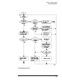
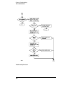
119 Troubleshooting 119
To use the flowcharts 120
To run the self-tests 123
To exit the test system 124
To test the cables 125
To test the auxiliary power 129
131 Replacing Assemblies 131
Tools Required 132
To remove the module 133
To replace the circuit board 134
To replace the module 135
To replace the probe cable 137
To return assemblies 138
139 Replaceable Parts 139
Replaceable Parts Ordering 140
Replaceable Parts List 141
Exploded View 143
145 Theory of Operation 145
Block-Level Theory 146
Self-Tests Description (16715/16/17A) 150
Self-Tests Description (16718/19A) 154
7
Contents
8
1
Accessories 10
Mainframe and Operating System 10
Specifications 11
Characteristics 12
Environmental Characteristics 13
Recommended Test Equipment 14
General Information
This chapter lists the accessories, the specifications and characteristics, and the
recommended test equipment.
Chapter 1: General Information
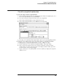
Accessories
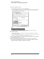
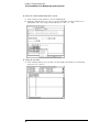
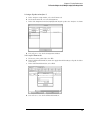
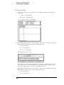
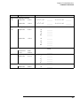
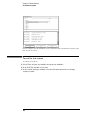
Accessories
The following accessories are supplied with the 16715/16/17/18/19A logic analyzer.
$FFHVVRULHV6XSSOLHG
3DUW1XPEHU
3UREH7LS$VVHPEO\4W\
*UDEEHUV4W\SDFNDJHV
([WUD3UREH/HDGV4W\SDFNDJH
([WUD3UREH*URXQGV4W\SDFNDJHV
3UREH&DEOHDQG3RG/DEHOV4W\
'RXEOH3UREH$GDSWHU4W\
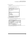
Mainframe and Operating System
The 16715/16/17A Logic Analyzer requires a 16700-series Logic Analysis System with
operating system version A.01.40.00 or higher. The 16718/19A Logic Analyzer requires an
16700-series Logic Analysis System with operating system version A.01.50 or higher.
NOTE
(DUOLHUYHUVLRQVRIWKH$$$PDLQIUDPHFRQWDLQHGRQO\WZRFRROLQJIDQVDQG
PLJKWQRWSURYLGHDGHTXDWHFRROLQJWRHQVXUHUHOLDEOHSHUIRUPDQFH,IWKHILUVWVL[GLJLWV
RIWKH$$VHULDOQXPEHUORFDWHGRQWKHEDFNRIWKHLQVWUXPHQWDUH86RU
KLJKHURUWKHILUVWVL[GLJLWVRIWKH$DUH86RUKLJKHUWKHLQVWUXPHQWLVD
WKUHHIDQPRGHODQGWKHUHLVVXIILFLHQWFRROLQJ
10
Chapter 1: General Information
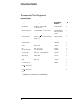
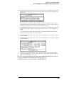
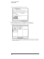
Specifications
Specifications
The specifications are the performance standards against which the product is tested.
7KUHVKROG$FFXUDF\
0D[LPXP6WDWH6SHHG
0LQLPXP0DVWHUWR0DVWHU&ORFN7LPH
P9RIWKUHVKROGVHWWLQJ
0+]
QV
6HWXS+ROG7LPHIRU'LIIHUHQW&ORFN6FKHPHV
6LQJOH&ORFN6LQJOH(GJH
6LQJOH&ORFN0XOWLSOH(GJHV
0XOWLSOH&ORFNV0XOWLSOH(GJHV
QVWKURXJKQVDGMXVWDEOHLQSV
LQFUHPHQWV
QVWKURXJKQVDGMXVWDEOHLQSV
LQFUHPHQWV
QVWKURXJKQVDGMXVWDEOHLQSV
LQFUHPHQWV
6SHFLILHGIRUDQLQSXWVLJQDO9+ 99/ 9DQGWKUHVKROG 9
)RUWKH$WKH0D[LPXP6WDWH6SHHGLV0+]DQGWKH0LQLPXP0DVWHUWR0DVWHU&ORFN7LPHLV
IRU6LQJOH&ORFN6LQJOH(GJHRU6LQJOH&ORFNRU0XOWLSOH(GJH&ORFNLQJ0RGH
11
Chapter 1: General Information
Characteristics
Characteristics
The characteristics are not specifications, but are included as additional information.
0D[LPXP6WDWH&ORFN5DWH
0D[LPXP6WDWH&ORFN7XUER5DWH
$RQO\
0D[LPXP&RQYHQWLRQDO7LPLQJ5DWH
&KDQQHO&RXQWSHU&DUG
&KDQQHO&RXQWSHU7KUHH&DUG0RGXOH
&KDQQHO&RXQWSHU)LYH&DUG0RGXOH
0HPRU\'HSWK$$
0HPRU\'HSWK$
0HPRU\'HSWK$
0HPRU\'HSWK$
)XOO&KDQQHO
+DOI&KDQQHO
0+]
0+]
1RWDSSOLFDEOH
1RWDSSOLFDEOH
0+]
.
.
.
.
0+]
.
.
.
.
+DOIFKDQQHOPRGHLVRQO\DYDLODEOHIRUWLPLQJDQDO\VLV
12
Chapter 1: General Information
Environmental Characteristics
Environmental Characteristics
3UREHV
0D[LPXP,QSXW9ROWDJH
9&$7,&$7, &DWHJRU\,VHFRQGDU\SRZHUOLQHLVRODWHGFLUFXLWV
$X[LOLDU\3RZHU
3RZHU7KURXJK&DEOHV
DPSDW9PD[LPXPSHUFDEOH
2SHUDWLQJ(QYLURQPHQW
7HPSHUDWXUH
+XPLGLW\
$OWLWXGH
9LEUDWLRQ
,QVWUXPHQW&WR&)WR)
3UREHOHDGVHWVDQGFDEOHV&WR&)WR)
,QVWUXPHQWSUREHOHDGVHWVDQGFDEOHVXSWRUHODWLYHKXPLGLW\DW
&)
7RPIW
2SHUDWLQJ5DQGRPYLEUDWLRQWR+]PLQXWHVSHUD[LV≈JUPV
1RQRSHUDWLQJ5DQGRPYLEUDWLRQWR+]PLQXWHVSHUD[LV≈J
UPVDQGVZHSWVLQHUHVRQDQWVHDUFKWR+]JSHDN
PLQXWHUHVRQDQWGZHOODWUHVRQDQFHVSHUD[LV
2SHUDWLQJSRZHUVXSSOLHGE\PDLQIUDPH
,QGRRUXVHRQO\
3ROOXWLRQ'HJUHH
13
Chapter 1: General Information
Recommended Test Equipment
Recommended Test Equipment
Equipment Required
5HFRPPHQGHG
0RGHO3DUW
8VH
0+]QVSXOVHZLGWK
SVULVHWLPH
$2SWLRQ
37
'LJLWL]LQJ2VFLOORVFRSH
≥*+]EDQGZLGWKSVULVHWLPH
$PDLQIUDPH
ZLWK$SOXJLQ
PRGXOH
3
)XQFWLRQ*HQHUDWRU
$FFXUDF\≤× IUHTXHQF\'&RIIVHW
YROWDJH9
%2SWLRQ
3
'LJLWDO0XOWLPHWHU
P9UHVROXWLRQDFFXUDF\
$
3
%1&%DQDQD&DEOH
3
%1&7HH
%1&PII
3
&DEOH
%1&PPLQFK
$
3
60$&RD[&DEOH4W\
≥*+]EDQGZLGWK
3
%1&&RD[&DEOH
%1&PP!*+]EDQGZLGWK
3
$GDSWHU4W\
60$P%1&I
3
$GDSWHU
60$I%1&P
3
&RXSOHU
%1&PP
3
3UREHV4W\
$
3
%1&7HVW&RQQHFWRU[
4W\
3
%1&7HVW&RQQHFWRU[
4W\
37
(TXLSPHQW
&ULWLFDO6SHFLILFDWLRQV
3XOVH*HQHUDWRU
$ $GMXVWPHQW3 3HUIRUPDQFH7HVWV7 7URXEOHVKRRWLQJ
,QVWUXFWLRQVIRUPDNLQJWKHVHWHVWFRQQHFWRUVDUHLQFKDSWHU´7HVWLQJ3HUIRUPDQFHµ
14
2
To inspect the module 17
To prepare the mainframe 18
To configure a one-card module 19
To configure a multi-card module 20
To install the module 26
To turn on the system 28
To test the module 28
To clean the module 29
Preparing for Use
This chapter gives you instructions for preparing the logic analyzer module for
use.
Chapter 2: Preparing for Use
Power Requirements
All power supplies required for operating the logic analyzer are supplied through
the backplane connector in the mainframe.
Operating Environment
The operating environment is listed in chapter 1. Note the non-condensing humidity
limitation. Condensation within the instrument can cause poor operation or malfunction.
Provide protection against internal condensation.
The logic analyzer module will operate at all specifications within the temperature and
humidity range given in chapter 1. However, reliability is enhanced when operating the
module within the following ranges:
Temperature: +20 °C to +35 °C (+68 °F to +95 °F)
Humidity: 20% to 80% non-condensing
Storage
Store or ship the logic analyzer in environments within the following limits:
•
Temperature: -40 °C to +75 °C (-40 °F to +167 °F)
•
Humidity: Up to 90% at 65 °C
•
Altitude: Up to 15,300 meters (50,000 feet)
Protect the module from temperature extremes which cause condensation on the
instrument.
16
Chapter 2: Preparing for Use
To inspect the module
To inspect the module
1 Inspect the shipping container for damage.
If the shipping container or cushioning material is damaged, keep them until you have
checked the contents of the shipment and checked the instrument mechanically and
electrically.
2 Check the supplied accessories.
Accessories supplied with the module are listed in chapter 1, "Accessories Supplied."
3 Inspect the product for physical damage.
Check the module and the supplied accessories for obvious physical or mechanical
defects. If you find any defects, contact your nearest Agilent Technologies Sales Office.
Arrangements for repair or replacement are made, at Agilent Technologies option,
without waiting for a claim settlement.
17
Chapter 2: Preparing for Use
To prepare the mainframe
To prepare the mainframe
CAUTION
7XUQRIIWKHPDLQIUDPHSRZHUEHIRUHUHPRYLQJUHSODFLQJRULQVWDOOLQJWKHPRGXOH
CAUTION
(OHFWURVWDWLFGLVFKDUJHFDQGDPDJHHOHFWURQLFFRPSRQHQWV8VHJURXQGHGZULVWVWUDSV
DQGPDWVZKHQSHUIRUPLQJDQ\VHUYLFHWRWKLVPRGXOH
1 Remove power from the instrument.
a
b
c
d
e
Exit all logic analysis sessions. In the session manager, select Shutdown.
At the query, select Power Down.
When the “OK to power down” message appears, turn the instrument off.
Disconnect the power cord.
Disconnect any input or output connections.
2 Plan your module configuration.
If you are installing a one-card module, use any available slot in the mainframe.
If you are installing a multi-card module, use adjacent slots in the mainframe.
3 Loosen the thumb screws.
Cards or filler panels below the slots intended for installation do not have to be removed.
Starting from the top, loosen the thumb screws on filler panels and cards that need to be
moved.
4 Starting from the top, pull the cards and filler panels that need to be moved
halfway out.
CAUTION
$OOPXOWLFDUGPRGXOHVZLOOEHFDEOHGWRJHWKHU3XOOWKHVHFDUGVRXWWRJHWKHU
5 Remove the cards and filler panels.
Remove the cards or filler panels that are in the slots intended for the module installation.
Push all other cards into the card cage, but not completely in. This is to get them out of
the way for installing the module.
Some modules for the Logic Analysis System require calibration if you move them to a
different slot. For calibration information, refer to the manuals for the individual modules.
18
Chapter 2: Preparing for Use
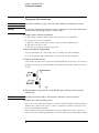
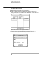
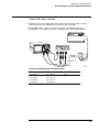
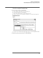
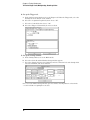
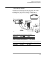
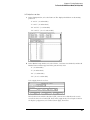
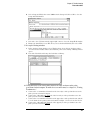
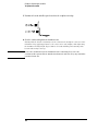
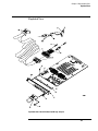
To configure a one-card module
To configure a one-card module
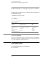
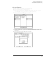
•
When shipped separately, the module is configured as a one-card module. The cables
should be connected as shown in the illustration below.
•
To configure a multicard module into one-card modules, remove the cables
connecting the cards. Then connect the free end of the 2x10 cable to the connector
labeled "Master" (J6) on each card (see figure below).
CAUTION
,I\RXSXOORQWKHIOH[LEOHULEERQSDUWRIWKH[FDEOH\RXPLJKWGDPDJHWKHFDEOH
DVVHPEO\8VLQJ\RXUWKXPEDQGILQJHUJUDVSWKHHQGVRIWKHFDEOHFRQQHFWRU$SSO\
SUHVVXUHWRWKHHQGVRIWKHFDEOHFRQQHFWRUWRGLVHQJDJHWKHPHWDOORFNLQJWDEVRIWKH
FRQQHFWRUIURPWKHFDEOHVRFNHWRQWKHERDUG7KHQSXOOWKHFRQQHFWRUIURPWKHFDEOH
VRFNHW
NOTE
6DYHXQXVHGFDEOHVIRUIXWXUHFRQILJXUDWLRQV
19
Chapter 2: Preparing for Use
To configure a multi-card module
To configure a multi-card module
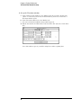
1 Plan the configuration. Multicard modules can only be connected as shown in
the illustration. Select the card that will be the master card, and set the
remaining cards aside.
2 Obtain two 2x40 cables from the accessory pouch for every expander card being
configured.
One Expander: Two 2x40 cables
Two Expanders: Four 2x40 cables
Three Expanders: Six 2x40 cables
Four Expanders: Eight 2x40 cables.
20
Chapter 2: Preparing for Use
To configure a multi-card module
3 Connect a 2x40 cable to the multicard cable connectors on the top of each card
in the multicard configuration.
4 On the expander cards, disconnect the end of the 2x10 cable that is plugged into
the connector labeled "Master."
CAUTION
,I\RXSXOORQWKHIOH[LEOHULEERQSDUWRIWKH[FDEOH\RXPLJKWGDPDJHWKHFDEOH
DVVHPEO\8VLQJ\RXUWKXPEDQGILQJHUJUDVSWKHHQGVRIWKHFDEOHFRQQHFWRU$SSO\
SUHVVXUHWRWKHHQGVRIWKHFDEOHFRQQHFWRUWRGLVHQJDJHWKHPHWDOORFNLQJWDEVRIWKH
FRQQHFWRUIURPWKHFDEOHVRFNHWRQWKHERDUG7KHQSXOOWKHFRQQHFWRUIURPWKHFDEOH
VRFNHW
21
Chapter 2: Preparing for Use
To configure a multi-card module
5 Begin stacking the cards together according to the drawing under step 1 on
page 20. While stacking, connect the free end of each 2x40 cable on the lower
card to the corresponding multicard connector on the bottom of the upper card,
on the underside of the card.
22
Chapter 2: Preparing for Use
To configure a multi-card module
6 Feed the free end of the 2x10 cables of the lower expander cards through the
access holes to the master card. Plug the 2x10 cables into J4 (bottom-most
expander in a five-card configuration) and J5 (expander that is next to the
master card) on the master card.
23
Chapter 2: Preparing for Use
To configure a multi-card module
7 Stack the remaining expander boards on top of the master board. While
stacking, connect the free end of each 2x40 cables on the lower card to the
corresponding connector on the bottom of the upper card.
24
Chapter 2: Preparing for Use
To configure a multi-card module
8 Feed the free end of the 2x10 cables of the expander cards through the access
holes to the master card. Plug the 2x10 cables into J7 (expander that is next to
the master card) and J8 (top-most expander in a four- or five-card configuration)
on the master card.
25
Chapter 2: Preparing for Use
To install the module
To install the module
1 Slide the cards above the slots for the module about halfway out of the
mainframe.
2 With the probe cables facing away from the instrument, slide the module
approximately halfway into the mainframe.
3 Slide the complete module into the mainframe, but not completely in.
Each card in the instrument is firmly seated and tightened one at a time in step 5.
4 Position all cards and filler panels so that the endplates overlap.
26
Chapter 2: Preparing for Use
To install the module
5 Seat the cards and tighten the thumbscrews.
Starting with the bottom card, firmly seat the cards into the backplane connector of the
mainframe. Keep applying pressure to the center of the card endplate while tightening
the thumbscrews finger-tight. Repeat this for all cards and filler panels starting at the
bottom and moving to the top.
CAUTION
&RUUHFWDLUFLUFXODWLRQNHHSVWKHLQVWUXPHQWIURPRYHUKHDWLQJ)RUFRUUHFWDLU
FLUFXODWLRQILOOHUSDQHOVPXVWEHLQVWDOOHGLQDOOXQXVHGFDUGVORWV.HHSDQ\H[WUDILOOHU
SDQHOVIRUIXWXUHXVH
27
Chapter 2: Preparing for Use
To turn on the system
To turn on the system
1 Connect the power cable to the mainframe.
2 Turn on the instrument power switch.
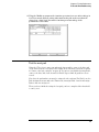
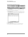
When you turn on the instrument power switch, the instrument performs powerup tests
that check mainframe circuitry. After the powerup tests are complete, the screen will
look similar to the sample screen below.
To test the module
The logic analyzer module does not require an operational accuracy calibration or
adjustment. After installing the module, you can test and use the module.
•
If you require a test to verify the specifications, start at the beginning of chapter 3,
"Testing Performance."
•
If you require a test to initially accept the operation, perform the self-tests in
chapter 3.
•
If the module does not operate correctly, go to the beginning of chapter 5,
"Troubleshooting."
28
Chapter 2: Preparing for Use
To clean the module
To clean the module
•
With the mainframe turned off and unplugged, use mild detergent and water to clean
the rear panel.
•
Do not attempt to clean the module circuit board.
29
Chapter 2: Preparing for Use
To clean the module
30
3
To Perform the Self-tests 33
To Set up the Test Connectors 35
To Set up the Test Equipment and the Analyzer 37
To Test the Threshold Accuracy 39
To Test the Single-clock, Single-edge, State Acquisition 46
To Test the Multiple-clock, Multiple-edge, State Acquisition 59
To Test the Single-clock, Multiple-edge, State Acquisition 72
To Test the Time Interval Accuracy 83
To Test the Multi-card Module 90
To Test the 333 MHz State Mode (16717/18/19A) 102
Performance Test Record 113
Testing Performance
This chapter tells you how to test the performance of the logic analyzer against
the specifications listed in chapter 1.
Chapter 3: Testing Performance
To ensure the logic analyzer is operating as specified, software tests (self-tests)
and manual performance tests are done. The logic analyzer is considered
performance-verified if all of the software tests and manual performance tests
have passed. The procedures in this chapter indicate what constitutes a “Pass”
status for each of the tests.
Test Strategy
This chapter shows the module being tested in an 16700-series mainframe with
operating system version A.02.00. For a complete test, start at the beginning with
the software tests and continue through to the end of the chapter. For an
individual test, follow the procedure in the test.
One-card Module. To perform a complete test on a one-card module, start at
the beginning of the chapter and follow each procedure.
Multi-card Module. To perform a complete test on a multi-card module,
perform the self-tests with the cards connected. Then, remove the multi-card
module from the mainframe and configure each card as a one-card module.
Install the one-card modules into the mainframe and perform the one-card
manual performance verification tests on each card. When the tests are complete,
remove the one-card modules, reconfigure them into a multi-card module,
reinstall it into the mainframe and perform the final multi-card test. For removal
instructions, see Chapter 6, “Replacing Assemblies.” For installation and
configuration instructions, see Chapter 2, “Preparing for Use.”
Test Interval
Test the performance of the module against specifications at two-year intervals.
Test Record Description
A performance test record for recording the results of each procedure is located
at the end of this chapter. Use the performance test record to gauge the
performance of the module over time.
Test Equipment
Each procedure lists the recommended test equipment. You can use equipment
other than the recommended test equipment that satisfies the specifications
given. However, the procedures are based on using the recommended model or
part number.
Instrument Warm-Up
Before testing the performance of the module, warm-up the instrument and the
test equipment for 30 minutes.
32
Chapter 3: Testing Performance
To Perform the Self-tests
To Perform the Self-tests
There are two types of self-tests: self-tests that automatically run at power-up,
and self-tests that you select on the screen. The self-tests verify the correct
operation of the logic analysis system. Self-tests can be performed all at once or
one at a time. While testing the performance of the logic analysis system, run the
self-tests all at once.
Perform the power-up tests
The logic analysis system automatically performs power-up tests when you apply power
to the instrument. Any errors are reported in the boot dialogue. Serious errors will
interrupt the boot process.
The power-up tests are designed to complement the instruments on-line Self Tests. Tests
that are performed during power-up are not repeated in the Self Tests.
The monitor, keyboard and mouse must be connected to the mainframe to observe the
results of the power-up tests.
NOTE
The 16700A does not require a monitor, or keyboard. The 16702B does not require a monitor,
mouse, or keyboard.
1 Disconnect all inputs and exit all logic analysis sessions.
In the Session Manager, select Shutdown. In the window, select Powerdown.
2 When the “OK to power down” message appears, turn off the power switch.
3 After a few seconds, turn the power switch back on. Observe the boot dialogue
for the following:
•
ensure all of the installed memory is recognized
•
any error messages
•
interrupt of the boot process with or without error message
A complete transcript of the boot dialogue is in the 16700-Series Logic Analysis System
Service Guide, Chapter 8, “Theory of Operation”.
4 During initialization, check for any failures.
If an error or an interrupt occurs, refer to the 16700-Series Logic Analysis System
Service Guide, Chapter 5, “Troubleshooting”.
33
Chapter 3: Testing Performance
To Perform the Self-tests
Perform the self-tests
The self-tests verify the correct operation of the logic analysis system and the
installed 16715/16/17/18/19A module. Self-tests can be performed all at once or
one at a time. While testing the performance of the logic analysis system, run the
self-tests all at once.
1 Launch the Self-Tests.
a In the System window, select System Admin.
b Under the Admin tab, select Self-Test. . .
c In the query pop-up, select Yes to exit the current session.
The Self-Test closes down the current session because the test algorithms leave the
system in an unknown state. Re-launching a session at the end of the tests will ensure
the system is properly initialized.
2 In the Self-Test window select Test All.
When the tests are finished, the Status will change to TEST passed or TEST failed. You
can find detailed information about the test results in the Status Message field of the SelfTest window.
The System CPU Board test returns Untested because the CPU tests require user action.
To test the CPU Board, select CPU Board, then select each test individually.
3 Select Quit to exit the Test menu.
4 In the Session Manager, select Start Session to re-launch a logic analysis session.
34
Chapter 3: Testing Performance
To Set up the Test Connectors
To Set up the Test Connectors
The test connectors connect the logic analysis system to the test equipment.
Materials Required
'HVFULSWLRQ
5HFRPPHQGHG3DUW 4W\
%1&I&RQQHFWRU
ΩUHVLVWRU
%HUJ6WULSE\
%HUJ6WULSE\
3UREH
-XPSHUZLUH
$
1 Build three test connectors using BNC connectors and 6-by-2 sections of Berg
strip.
a
b
c
d
e
f
Solder a jumper wire to all pins on one side of the Berg strip.
Solder a jumper wire to all pins on the other side of the Berg strip.
Solder two resistors to the Berg strip, one at each end between the end pins.
Solder the center of the BNC connector to the center pin of one row on the Berg strip.
Solder the ground tab of the BNC connector to the center pin of the other row on the
Berg strip.
On two of the test connectors, solder a 20:1 probe. The probe ground goes to the same
row of pins on the test connector as the BNC ground tab.
35
Chapter 3: Testing Performance
To Set up the Test Connectors
2 Build one test connector using a BNC connector and a 17-by-2 section of Berg
strip.
a
b
c
d
36
Solder a jumper wire to all pins on one side of the Berg strip.
Solder a jumper wire to all pins on the other side of the Berg strip.
Solder the center of the BNC connector to the center pin of one row on the Berg strip.
Solder the ground tab of the BNC connector to the center pin of the other row on the
Berg strip.
Chapter 3: Testing Performance
To Set up the Test Equipment and the Analyzer
To Set up the Test Equipment and the Analyzer
Before testing the specifications of the 16715/16/17/18/19A logic analyzer, the
test equipment and the logic analysis system must be set up and configured.
These instructions include detailed steps for initially setting up the required test
equipment and the logic analysis system. Before performing any or all of the
following tests in this chapter, the following steps must be followed.
NOTE
Multi-card modules must be separated into single-card modules.
Equipment Required
(TXLSPHQW
&ULWLFDO6SHFLILFDWLRQV
5HFRPPHQGHG0RGHO3DUW
3XOVH*HQHUDWRU
'LJLWL]LQJ2VFLOORVFRSH
'LJLWDO0XOWLPHWHU
)XQFWLRQ*HQHUDWRU
0K]QVSXOVHZLGWKSVULVHWLPH
≥*+]EDQGZLGWKSVULVHWLPH
P9UHVROXWLRQDFFXUDF\
'&RIIVHWYROWDJH9
$RSWLRQ
$Z$
$
%2SWLRQ
Set up the equipment
1 Turn on the required test equipment listed in the table above. Let them warm up
for 30 minutes before beginning any test.
2 Turn on the logic analysis system.
a Connect the keyboard, mouse, and monitor to the rear panel of the logic analysis
system mainframe.
NOTE
The 16700A does not require a monitor, or keyboard. The 16702B does not require a monitor,
mouse, or keyboard.
b Plug in the power cord to the power connector on the rear panel of the mainframe.
c Turn on the main power switch on the mainframe front panel.
3 Set up the logic analysis system.
a Open the Session Manager window and select “Start Session”.
b In the Logic Analysis System window, select the module icon, then select Setup. A
Setup window opens.
c In the Setup window, select Window, then select Slot n: Analyzer<n> (where “n” is the
slot the module under test is installed), then select Listing. A Listing window opens.
d In the Analyzer<n> Setup window, select the Sampling tab.
37
Chapter 3: Testing Performance
To Set up the Test Equipment and the Analyzer
4 Set up the pulse generator according to the following table.
7LPHEDVH
&KDQQHO
7ULJJHU
&KDQQHO
0RGH,QW
3HULRGQV
0RGH3XOVH
'LYLGH3XOVH÷ :LGWKQV
+LJK9
/RZ9
&203'LVDEOHG
/('2II
'LYLGH'LYLGH÷ $PSO9
2IIV9
0RGH6TXDUH
'HOD\QV
+LJK9
/RZ9
&203'LVDEOHG
/('2II
5 Set up the oscilloscope.
a Select Setup, then choose Default Setup.
b Configure the oscilloscope according to the following table.
Oscilloscope Setup
$FTXLVLWLRQ
'LVSOD\
7ULJJHU
>6KLIW@∆7LPH
$YHUDJLQJ2Q
RIDYHUDJHV
*UDWLFXOHJUDSKV
/HYHOP9
6WRSVUFFKDQQHO>(QWHU@
&KDQQHO
&KDQQHO
'HILQHPHDV
([WHUQDO6FDOH$WWHQXDWLRQ ([WHUQDO6FDOH$WWHQXDWLRQ 7KUHVKROGVXVHUGHILQHG
6FDOHP9GLY
6FDOHP9GLY
8QLWV9ROWV
2IIVHW9
2IIVHW9
8SSHUP9
0LGGOH9
/RZHU9
Allow the logic analysis system to warm up for 30 minutes before beginning any of
the following tests.
38
Chapter 3: Testing Performance
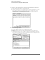
To Test the Threshold Accuracy
To Test the Threshold Accuracy
Testing the threshold accuracy verifies the performance of the following
specification:
•
Clock and data channel threshold accuracy
These instructions include detailed steps for testing the threshold settings of Pod
1. After testing Pod 1, connect and test the rest of the pods one at a time. To test
the next pod, follow the detailed steps for Pod 1, substituting the next pod for
Pod 1 in the instructions.
Equipment Required
(TXLSPHQW
&ULWLFDO6SHFLILFDWLRQV
5HFRPPHQGHG0RGHO3DUW
'LJLWDO0XOWLPHWHU
)XQFWLRQ*HQHUDWRU
%1&%DQDQD&DEOH
%1&7HH
%1&&DEOH
%1&7HVW&RQQHFWRU[
P9UHVROXWLRQDFFXUDF\
'&RIIVHWYROWDJH9
$
%2SWLRQ
Set up the equipment
1 If you have not already done so, perform the procedure described in “To Set up
the Test Equipment and the Analyzer” on page 37.
2 Set up the function generator.
a Set up the function generator to provide a DC offset voltage at the Main Signal output.
b Disable any AC voltage to the function generator output, and enable the high voltage
output.
c Monitor the function generator DC output voltage with the multimeter.
39
Chapter 3: Testing Performance
To Test the Threshold Accuracy
Set up the logic analyzer
1 In the Analyzer Setup window, select the Format tab.
2 Under the Format tab, select Pod Assignment. Unassign the pods that are
assigned to Analyzer 2. To unassign the pods, highlight and drag the pods to the
Unassigned Pods column.
Select Close to close the Pod Assignment Window.
3 Under the Format tab, select the Threshold field under Pod 1. Select the
checkbox next to Apply Threshold Setting to all pods to deselect.
40
Chapter 3: Testing Performance
To Test the Threshold Accuracy
Connect the logic analyzer
1 Using the 17-by-2 test connector, BNC cable, and probe tip assembly, connect
the data and clock channels of Pod 1 to one side of the BNC Tee.
2 Using a BNC-banana cable, connect the voltmeter to the other side of the BNC
Tee.
3 Connect the BNC Tee to the Main Signal output of the function generator.
41
Chapter 3: Testing Performance
To Test the Threshold Accuracy
Test the ECL threshold
1 In the Pod Threshold window, select ECL.
2 On the function generator front panel, enter -1.214 V ±1 mV DC offset. Use the
multimeter to verify the voltage.
The activity indicators for Pod 1 should show all data channels and the J-clock channel at
a logic high.
7KUHVKROG)LHOG
3 Using the Modify down arrow on the function generator, decrease offset voltage
in 1-mV increments until all activity indicators for the pod under test show the
channels are at a logic low. Record the function generator voltage in the
performance test record.
42
Chapter 3: Testing Performance
To Test the Threshold Accuracy
4 Using the Modify up arrow on the function generator, increase offset voltage in
1-mV increments until all activity indicators for the pod under test show the
channels are at a logic high. Record the function generator voltage in the
performance test record.
43
Chapter 3: Testing Performance
To Test the Threshold Accuracy
Test the 0 V User threshold
1 In the Pod Threshold window, select User Defined. In the numeric field, enter
0 V.
2 On the function generator front panel, enter +0.067 V ±1 mV DC offset. Use the
multimeter to verify the voltage.
The activity indicators for the pod under test should show all data channels and the Jclock channel at a logic high.
3 Using the Modify down arrow on the function generator, decrease offset voltage
in 1-mV increments until all activity indicators for the pod under test show the
channels at a logic low. Record the function generator voltage in the
performance test record.
44
Chapter 3: Testing Performance
To Test the Threshold Accuracy
4 Using the Modify up arrow on the function generator, increase offset voltage in
1-mV increments until all activity indicators for the pod under test show the
channels at a logic high. Record the function generator voltage in the
performance test record.
Test the next pod
Using the 17-by-2 test connector and probe tip assembly, connect the data and
clock channels of the next pod to the output of the function generator as shown
in “Connect the logic analyzer” on page 41. If you have just finished testing Pod 1,
connect the data and clock channels of Pod 2. Repeat until all pods have been
tested.
Note that the pod under test must be assigned to the analyzer. For Pod 3, use the
Pod Assignment menu under the Format tab, unassign Pods 1 and 2 and assign
Pods 3 and 4 to Analyzer 1.
When you have finished testing the last pod, you have completed the threshold
accuracy test.
45
Chapter 3: Testing Performance
To Test the Single-clock, Single-edge, State Acquisition
To Test the Single-clock, Single-edge, State Acquisition
Testing the single-clock, single-edge, state acquisition verifies the performance of
the following specifications:
•
Minimum master to master clock time
•
Maximum state acquisition speed
•
Setup/Hold time
This test checks a combination of data channels using a single-edge clock at two
selected setup/hold times.
Equipment Required
5HFRPPHQGHG0RGHO
3DUW
(TXLSPHQW
&ULWLFDO6SHFLILFDWLRQV
3XOVH*HQHUDWRU
'LJLWL]LQJ2VFLOORVFRSH
$GDSWHU
60$&RD[&DEOH4W\
&RXSOHU4W\
%1&7HVW&RQQHFWRU[4W\
0K]QVSXOVHZLGWKSVULVHWLPH $RSWLRQ
≥*+]EDQGZLGWKSVULVHWLPH
$Z$
60$P%1&I
%1&PP
Set up the equipment
If you have not already done so, do the procedure “To Set up the Test Equipment
and the Analyzer” on page 37. Ensure that the pulse generator and oscilloscope
are set up according to the tables in that section.
Set up the logic analyzer
1 Set up the Sampling tab.
a In the Analyzer setup window, select the Sampling tab.
b Select State Mode.
46
Chapter 3: Testing Performance
To Test the Single-clock, Single-edge, State Acquisition
2 Assign all pods to Analyzer 1.
a In the Analyzer setup window, select the Format tab.
b Under the Format tab, select Pod Assignment.
c In the Pod Assignment window, highlight and drag the pods to the Analyzer 1 column.
d Select Close to close the Pod Assignment window.
3 Set up the Format tab.
a Under one of the pod fields, select TTL.
b In the Pod Threshold window, ensure the Apply threshold setting to all pods checkbox
is checked.
c In the Pod Threshold window, select ECL.
d Select Close to close the Pod Threshold window.
47
Chapter 3: Testing Performance
To Test the Single-clock, Single-edge, State Acquisition
4 Set up the Trigger tab.
a In the Analyzer setup window, select the Trigger tab. Under the Trigger tab, select the
Settings tab.
b Select the Acquisition Depth field, then choose “8K”.
c Select the Trigger Position field, then choose Start.
d Select the Count field, then select “Off”.
5 Set up the Listing window.
a In the Listing window, select the Markers tab.
b Select the G1: field and the Markers Setup window appears.
c Select the Time field associated with G1, and choose Pattern. Select the Time field
associated with G2, and select Pattern.
Note: Leave the Marker Setup window open. You will be entering numeric values
in the “occurs” field after acquiring the test data.
48
Chapter 3: Testing Performance
To Test the Single-clock, Single-edge, State Acquisition
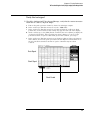
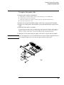
Connect the logic analyzer
1 Using the 6-by-2 test connectors, connect the logic analyzer clock and data
channels listed in the following tables to the pulse generator.
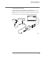
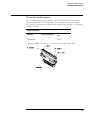
2 Using SMA cables, connect channel 1, channel 2, and trigger from the
oscilloscope to the pulse generator according to the following illustration.
Connect the 16715/16/17/18/19A to the Pulse Generator
$&K2XWSXW
$&K2XWSXW
$&K2XWSXW
3RGFKDQQHO
3RGFKDQQHO
3RGFKDQQHO
3RGFKDQQHO
3RGFKDQQHO
3RGFKDQQHO
3RGFKDQQHO
3RGFKDQQHO
-FORFN
49
Chapter 3: Testing Performance
To Test the Single-clock, Single-edge, State Acquisition
3 Activate the data channels that are connected according to the previous table.
a In the Analyzer setup window, select the Format tab.
b Under the Format tab, select the field showing the channel assignments for one of the
pods being tested, then choose Individual. Select the data channels to be tested
(channels 11 and 3 of each pod). An asterisk means that a channel is turned on.
Follow this step for the remaining pods to be tested.
4 Configure the trigger pattern.
a Select the Trigger tab, then choose the Trigger Functions tab.
b In the General State field, select Store nothing until pattern occurs. Then select
Replace.
c Under Trigger Sequence, locate the Label 1 = trigger pattern field. Enter “AA” in the
trigger pattern field. The trigger function should now read Store nothing until Label 1
= AA Hex occurs then Trigger and fill memory.
50
Chapter 3: Testing Performance
To Test the Single-clock, Single-edge, State Acquisition
Verify the test signal
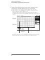
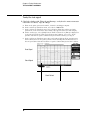
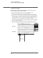
1 Check the clock period. Using the oscilloscope, verify that the master-to-master
clock time is 5.988 ns, +0 ps or -100 ps.
a Turn on the pulse generator channel 1, channel 2, and trigger outputs.
b In the oscilloscope Timebase menu, select Scale: 1.000 ns/div.
c In the oscilloscope Timebase menu, select Position. Using the oscilloscope knob,
position the clock waveform so that a rising edge appears at the left of the display.
d On the oscilloscope, select [Shift] Period: channel 2, then select [Enter] to display the
clock period (Period(2)). If the period is more than 5.988 ns, go to step e. If the
period is less than or equal to 5.988 ns but greater than 5.888 ns, go to step 2.
e In the oscilloscope Timebase menu, increase Position 5.988 ns. If the period is more
than 5.988 ns, decrease the pulse generator Period in 10 ps increments until one of
the two periods measured is less than or equal to 5.988 ns but greater than
5.888 ns.
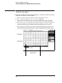
Data Signal
Clock Signal
Clock Period
51
Chapter 3: Testing Performance
To Test the Single-clock, Single-edge, State Acquisition
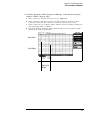
2 Check the data pulse width. Using the oscilloscope, verify that the data pulse
width is 2.500 ns, +0 ps or -50 ps.
a In the oscilloscope Timebase menu, select Scale: 1.000 ns/div.
b In the oscilloscope Timebase menu, select Position. Using the oscilloscope knob,
position the data waveform so that the waveform is centered on the screen.
c On the oscilloscope, select [Shift] + width: channel 1, then select [Enter] to display the
data signal pulse width (+ width(1)).
d If the pulse width is outside the limits, adjust the pulse generator channel 2 width
until the pulse width is within limits.
Data Signal
Clock Signal
Data Pulse
Width
52
Chapter 3: Testing Performance
To Test the Single-clock, Single-edge, State Acquisition
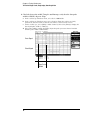
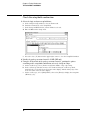
Check the setup/hold combination
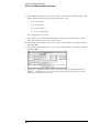
1 Select the logic analyzer setup/hold time.
a
b
c
d
In the Analyzer setup window, select the Format tab.
Under the Format tab, select Setup/Hold.
In the Setup and Hold window, ensure All bits is selected.
Enter the setup time of the setup/hold combination to be tested in the Setup: field.
Setup/Hold Combinations
QV
QV
e Select the close (X) button in the upper-right corner to close the Setup/Hold window.
2 Disable the pulse generator channel 1 COMP (LED off).
53
Chapter 3: Testing Performance
To Test the Single-clock, Single-edge, State Acquisition
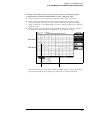
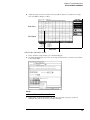
3 Using the Delay mode of the pulse generator channel 1, position the pulses
according to the setup/hold combination selected, +0.0 ps or -50 ps.
a On the Oscilloscope, select [Define meas] Define ∆Time - Stop edge: rising.
b In the oscilloscope timebase menu, select Position. Using the oscilloscope knob,
position both a clock and a data waveform on the display, with the rising edge of the
clock waveform centered on the display.
c On the oscilloscope, select [Shift] ∆ Time, then select [Enter] to display the setup time
(∆Time(1)-(2)).
d Adjust the pulse generator channel 1 Delay until the pulses are aligned according the
setup time of the setup/hold combination selected, +0.0 ps or -50 ps.
Data Signal
Clock Signal
Setup Time
Disregard the Period(2) value. The settings provided in this procedure may measure
the period from falling edge to falling edge, which is not a valid measurement.
54
Chapter 3: Testing Performance
To Test the Single-clock, Single-edge, State Acquisition
4 Select the clock to be tested.
a In the Analyzer setup window, select the Sampling tab.
b Under the Sampling tab, select the clock edge field under the clock to be tested. Then
select Rising Edge. Turn off all other clocks. The first time through this test, select the
first clock and edge.
Clocks
-↑
c
.↑
/↑
0↑
Connect the clock input channel to be tested to the pulse generator channel 1
OUTPUT. Disconnect all other clock input channels.
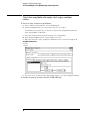
5 Verify the test data.
a In the Listing window, select the Run icon. The display should show an alternating
pattern of “AA” and “55”.
55
Chapter 3: Testing Performance
To Test the Single-clock, Single-edge, State Acquisition
b In the Marker Setup window, select the Define... field associated with G1, and the G1
Marker Pattern window appears. In the pattern field, enter “AA”. Select Apply, then
Close.
If the Label selection field reads Label1_TZ, you must select Label1 for the search
term. To do this, select Label1_TZ; then, in the popup menu, select Replace label. In
the Replace popup menu, select Label1, then Apply, then Close.
c
In the Marker Setup window, select the Define... field associated with G2, and the G2
Marker Pattern window appears. In the pattern field, enter “55”. Select Apply, then
Close.
If the Label selection field reads Label1_TZ, you must select Label1 for the search
term. Follow the same procedure as in b above.
d In the Marker Setup window, select the ‘occurs’ value field that corresponds to marker
G1. Enter 4095.
e In the Marker Setup window, select the ‘occurs’ value field that corresponds to marker
G2. Enter 4096.
f
Select Close to apply the marker values to the data. If the “Pattern NOT found for
marker…” error message does not appear, then the test passes. Record the Pass or
Fail in the performance test record.
6 Repeat steps 4 and 5 for the next clock edge listed in the table in step 4, until all
listed clock edges have been tested.
56
Chapter 3: Testing Performance
To Test the Single-clock, Single-edge, State Acquisition
7 Enable the pulse generator channel 1 COMP (LED on).
8 Using the Delay mode of the pulse generator channel 1, position the pulses
according to the setup/hold combination selected, +0.0 ps or -50 ps.
a On the Oscilloscope, select [Define meas] Define ∆Time - Stop edge: falling.
b On the oscilloscope, select [Shift] ∆Time. Select Start src: channel 1, then select
[Enter] to display the setup time (∆Time(1)-(2)).
c Adjust the pulse generator channel 1 Delay until the pulses are aligned according to
the setup time of the setup/hold combination selected, +0.0 ps or -50 ps.
Data Signal
Clock Signal
Setup Time
Disregard the Period(2) value. The settings provided in this procedure may measure
the period from rising edge to rising edge, which is not a valid measurement.
57
Chapter 3: Testing Performance
To Test the Single-clock, Single-edge, State Acquisition
9 Select the clock to be tested.
a In the Analyzer setup window, select the Sampling tab.
b Under the Sampling tab, select the clock edge field under the clock to be tested. Then
select Falling Edge. The first time through this test, select the first clock and edge.
Ensure all other clocks are turned off.
Clocks
-↓
c
.↓
/↓
0↓
Connect the clock input channel to be tested to the pulse generator channel 1
OUTPUT. Disconnect all other clock input channels.
10 Verify the test data.
a In the Listing window, select the Run icon. The display should show an alternating
pattern of “AA” and “55”.
b If the “Pattern NOT found for marker...” error message does not appear, then the test
passes. Record the Pass or Fail in the performance test record.
11 Repeat steps 9 and 10 for the next clock edge listed in the table in step 9, until all
listed clock edges have been tested.
12 If the setup/hold used for the previous steps was 4.5/-2.0 ns, repeat steps 1
through 11 using setup/hold -2.0/4.5 ns. If the setup/hold used for the previous
steps was -2.0/4.5 ns, continue on with the next section.
58
Chapter 3: Testing Performance
To Test the Multiple-clock, Multiple-edge, State Acquisition
To Test the Multiple-clock, Multiple-edge, State
Acquisition
Testing the multiple-clock, multiple-edge, state acquisition verifies the
performance of the following specifications:
•
Minimum master to master clock time
•
Maximum state acquisition speed
•
Setup/Hold time
This test checks a combination of data channels using multiple clocks at two
selected setup/hold times.
Equipment Required
(TXLSPHQW
&ULWLFDO6SHFLILFDWLRQV
3XOVH*HQHUDWRU
'LJLWL]LQJ2VFLOORVFRSH
$GDSWHU
60$&RD[&DEOH4W\
&RXSOHU4W\
%1&7HVW&RQQHFWRU[4W\
0K]QVSXOVHZLGWKSVULVHWLPH
≥*+]EDQGZLGWKSVULVHWLPH
60$P%1&I
%1&PP
5HFRPPHQGHG0RGHO
3DUW
$RSWLRQ
$Z $
Set up the equipment
1 If you have not already done so, do the procedure “To Set up the Test Equipment
and the Analyzer” on page 37. Ensure that the pulse generator and oscilloscope
are set up according to the tables in that section.
2 Change the pulse generator channel 2 width to 3.000 ns.
Set up the logic analyzer
Perform the following steps if you have not already done so for the previous test.
1 Set up the Sampling tab.
a In the Analyzer setup window, select the Sampling tab.
b Select State Mode.
59
Chapter 3: Testing Performance
To Test the Multiple-clock, Multiple-edge, State Acquisition
2 Assign all pods to Analyzer 1.
a In the Analyzer setup window, select the Format tab.
b Under the Format tab, select Pod Assignment.
c In the Pod Assignment window, highlight and drag the pods to the Analyzer 1 column.
d Select Close to close the Pod Assignment window.
3 Set up the Format tab.
a Under one of the pod fields, select TTL.
b In the Pod Threshold window, ensure the Apply threshold setting to all pods checkbox
is checked.
c In the Pod Threshold window, select ECL.
d Select Close to close the Pod Threshold window.
60
Chapter 3: Testing Performance
To Test the Multiple-clock, Multiple-edge, State Acquisition
4 Set up the Trigger tab.
a In the Analyzer setup window, select the Trigger tab. Under the Trigger tab, select the
Settings tab.
b Select the Acquisition Depth field, then choose “8K”.
c Select the Count field, then choose “Off”.
d Select the Trigger Position field, then choose Start.
5 Set up the Listing window.
a In the Listing window, select the Markers tab.
b Select the G1: field and the Markers Setup window appears.
c Select the Time field associated with G1, and choose Pattern. Select the Time field
associated with G2, and choose Pattern.
Note: Leave the Marker Setup window open. You will be entering numeric values in the
“occurs” field after acquiring the test data.
61
Chapter 3: Testing Performance
To Test the Multiple-clock, Multiple-edge, State Acquisition
Connect the logic analyzer
1 Using the 6-by-2 test connectors, connect the logic analyzer clock and data
channels listed in the following table to the pulse generator.
2 Using SMA cables, connect channel 1, channel 2, and trigger from the
oscilloscope to the pulse generator according to the following illustration.
Connect the 16715/16/17/18/19A to the Pulse Generator
$&K2XWSXW
$&K2XWSXW
$&K2XWSXW
3RGFKDQQHO
3RGFKDQQHO
3RGFKDQQHO
3RGFKDQQHO
3RGFKDQQHO
3RGFKDQQHO
3RGFKDQQHO
3RGFKDQQHO
-FORFN
.FORFN
/FORFN
0FORFN
62
Chapter 3: Testing Performance
To Test the Multiple-clock, Multiple-edge, State Acquisition
3 Activate the data channels that are connected according to the previous table.
a In the Analyzer setup window, select the Format tab.
b Under the Format tab, select the field showing the channel assignments for one of the
pods being tested, then choose Individual. Select the data channels to be tested
(channels 11 and 3 of each pod). An asterisk means that a channel is turned on.
Follow this step for the remaining pods to be tested.
4 Configure the trigger pattern.
a Select the Trigger tab, then choose the Trigger Functions tab.
b In the General State field, select Store nothing until pattern occurs. Then select
Replace.
c Under Trigger Sequence, locate the Label 1 = trigger pattern field. Enter “AA” in the
trigger pattern field. The trigger function should now read Store nothing until Label 1
= AA Hex occurs then Trigger and fill memory.
63
Chapter 3: Testing Performance
To Test the Multiple-clock, Multiple-edge, State Acquisition
Verify the test signal
1 Check the clock period. Using the oscilloscope, verify that the master-to-master
clock time is 5.988 ns, +0 ps or -100 ps.
a Turn on the pulse generator channel 1, channel 2, and trigger outputs.
b In the oscilloscope Timebase menu, select Scale: 1.000 ns/div.
c In the oscilloscope Timebase menu, select Position. Using the oscilloscope knob,
position the clock waveform so that a rising edge appears at the left of the display.
d On the oscilloscope, select [Shift] Period: channel 2, then select [Enter] to display the
clock period (Period(2)). If the period is more than 5.988 ns, go to step e. If the
period is less than or equal to 5.988 ns but greater than 5.888 ns, go to step 2.
e In the oscilloscope Timebase menu, increase Position 5.988 ns. If the period is more
than 5.988 ns, decrease the pulse generator Period in 10 ps increments until one of
the two periods measured is less than or equal to 5.988 ns but greater than 5.888 ns.
Data Signal
Clock Signal
Clock Period
64
Chapter 3: Testing Performance
To Test the Multiple-clock, Multiple-edge, State Acquisition
2 Check the data pulse width. Using the oscilloscope, verify that the data pulse
width is 3.000 ns, +0 ps or - 50 ps.
a In the oscilloscope Timebase menu, select Scale: 1.000 ns/div.
b In the oscilloscope Timebase menu, select Position. Using the oscilloscope knob,
position the data waveform so that the waveform is centered on the screen.
c On the oscilloscope, select [Shift] + width: channel 1, then select [Enter] to display the
data signal pulse width (+ width (1)).
d If the pulse width is outside the limits, adjust the pulse generator channel 2 width
until the pulse width is within limits.
Data Signal
Clock Signal
Data Pulse
Width
65
Chapter 3: Testing Performance
To Test the Multiple-clock, Multiple-edge, State Acquisition
Check the setup/hold with single clock edges, multiple
clocks
1 Select the logic analyzer setup/hold time.
a In the Analyzer setup window, select the Sampling tab.
b Under the Sampling tab, select and activate any two clock edges.
You must have two single-edge clocks selected before the Setup/Hold window will
allow a Setup/Hold of 5.0/-2.0 ns.
c Select the Format tab. Under the Format tab, select Setup/Hold.
d In the Setup and Hold window, ensure All bits is selected.
e Enter the setup time of the setup/hold combination to be tested in the Setup: field.
6HWXS+ROG&RPELQDWLRQV
QV
QV
f
Select the close (X) button in the upper-right corner to close the Setup/Hold window.
2 Disable the pulse generator channel 1 COMP (LED off).
66
Chapter 3: Testing Performance
To Test the Multiple-clock, Multiple-edge, State Acquisition
3 Using the Delay mode of the pulse generator channel 1, position the pulses
according to the setup/hold combination selected, +0.0 ps or -50 ps.
a On the Oscilloscope, select [Define meas] Define ∆ Time - Stop edge: rising.
b In the oscilloscope timebase menu, select Position. Using the oscilloscope knob,
position the rising edge of the clock waveform so that it is centered on the display.
c On the oscilloscope, select [Shift] ∆ Time, then select [Enter] to display the setup time
(∆ Time(1)-(2)).
d Adjust the pulse generator channel 1 Delay until the pulses are aligned according to
the setup time of the setup/hold combination selected, +0.0 ps or -50 ps.
Data Signal
Clock Signal
Setup Time
Disregard the Period(2) value. The settings provided in this procedure may measure
the period from falling edge to falling edge, which is not a valid measurement.
67
Chapter 3: Testing Performance
To Test the Multiple-clock, Multiple-edge, State Acquisition
4 Select the clock combination to be tested.
a In the Analyzer setup window, select the Sampling tab.
b Under the Sampling tab, select the clock edge field under each clock. Then select
Rising Edge. The clock setup field should show J↑ + K↑ + L↑ + M↑.
5 Verify the test data.
a In the Listing window, select the Run icon. The display should show an alternating
pattern of “AA” and “55”.
68
Chapter 3: Testing Performance
To Test the Multiple-clock, Multiple-edge, State Acquisition
b In the Marker Setup window, select the Define... field associated with G1, and the G1
Marker Pattern window appears. In the pattern field, enter “AA”. Select Apply, then
select Close.
If the Label selection field reads Label1_TZ, you must select Label1 for the search
term. To do this, select Label1_TZ; then, in the popup menu, select Replace label. In
the Replace popup menu, select Label1, then Apply, then Close.
c
In the Marker Setup window, select the Define... field associated with G2, and the G2
Marker Pattern window appears. In the pattern field, enter “55”. Select Apply, then
Close.
If the Label selection field reads Label1_TZ, you must select Label1 for the search
term. Follow the same procedure as in b above.
d In the Marker Setup window, select the ‘occurs’ value field that corresponds to marker
G1. Enter 4095.
e In the Marker Setup window, select the ‘occurs’ value field that corresponds to marker
G2. Enter 4096.
f
Select Close to apply the marker values to the data. If the “Pattern NOT found for
marker...” error message does not appear, then the test passes. Record the Pass or
Fail in the performance test record.
6 Repeat steps 4 and 5 for the next clock edge combination listed in the table in
step 4, until both clock combinations have been tested.
7 Enable the pulse generator channel 1 COMP (LED on).
69
Chapter 3: Testing Performance
To Test the Multiple-clock, Multiple-edge, State Acquisition
8 Using the Delay mode of the pulse generator channel 1, position the pulses
according to the setup/hold combination selected, +0.0 ps or -50 ps.
a On the Oscilloscope, select [Define meas] Define ∆Time - Stop edge: falling.
b On the oscilloscope, select [Shift] ∆Time. Select Start src: channel 1, then select
[Enter] to display the setup time (∆Time(1)-(2)).
Adjust the pulse generator channel 1 Delay until the pulses are aligned
according to the setup time of the setup/hold combination selected, +0.0 ps or
-50 ps.
Data Signal
Clock Signal
Setup Time
Disregard the Period(2) value. The settings provided in this procedure may measure
the period from rising edge to rising edge, which is not a valid measurement.
70
Chapter 3: Testing Performance
To Test the Multiple-clock, Multiple-edge, State Acquisition
9 Select the clock combination to be tested.
a In the Analyzer setup window, select the Sampling tab.
b Under the Sampling tab, select the clock edge field under each clock. Then select
Falling Edge. The clock setup field should show J↓ + K↓ + L↓ + M↓.
10 Verify the test data.
a In the Listing window, select the Run icon. The display should show an alternating
pattern of “AA” and “55”.
b If the “Pattern NOT found for marker...” error message does not appear, then the test
passes. Record the Pass or Fail in the performance test record.
11 Repeat steps 9 and 10 for the next clock combination listed in the table in step 9,
until both clock combinations have been tested.
12 If the setup/hold used for the previous steps was 5.0/-2.0 ns, repeat steps 1
through 11 using setup/hold -1.5/4.5 ns. If the setup/hold used for the previous
steps was -1.5/4.5 ns, continue on with the next section.
71
Chapter 3: Testing Performance
To Test the Single-clock, Multiple-edge, State Acquisition
To Test the Single-clock, Multiple-edge, State
Acquisition
Testing the single-clock, multiple-edge, state acquisition verifies the performance
of the following specifications:
•
Minimum master to master clock time
•
Maximum state acquisition speed
•
Setup/Hold time
This test checks a combination of data channels using a multiple-edge single
clock at two selected setup/hold times.
Equipment Required
5HFRPPHQGHG0RGHO
3DUW
(TXLSPHQW
&ULWLFDO6SHFLILFDWLRQV
3XOVH*HQHUDWRU
'LJLWL]LQJ2VFLOORVFRSH
$GDSWHU
60$&RD[&DEOH4W\
&RXSOHU4W\
%1&7HVW&RQQHFWRU[4W\
0K]QVSXOVHZLGWKSVULVHWLPH $RSWLRQ
≥*+]EDQGZLGWKSVULVHWLPH
$Z$
60$P%1&I
%1&PP
Set up the equipment
1 If you have not already done so, do the procedure “To Set up the Test Equipment
and the Analyzer” on page 37. Use the pulse generator settings listed below.
2 Make the following changes to the pulse generator configuration.
7LPHEDVH
&KDQQHO
3HULRGQV
'LYLGH38/6(÷
:LGWKQV
Set up the logic analyzer
Perform the following steps if you have not done so for the previous tests.
1 Set up the Sampling tab.
a In the Analyzer window, select the Sampling tab.
b Select State Mode.
72
Chapter 3: Testing Performance
To Test the Single-clock, Multiple-edge, State Acquisition
2 Assign all pods to Analyzer 1.
a In the Analyzer setup window, select the Format tab.
b Under the Format tab, select Pod Assignment.
c In the Pod Assignment window, highlight and drag the pods to the Analyzer 1 column.
d Select Close to close the Pod Assignment window.
3 Set up the Format tab.
a Under one of the pod fields, select TTL.
b In the Pod Threshold window, ensure the Apply threshold setting to all pods checkbox
is checked.
c In the Pod Threshold window, select ECL.
d Select Close to close the Pod Threshold window.
73
Chapter 3: Testing Performance
To Test the Single-clock, Multiple-edge, State Acquisition
4 Set up the Trigger tab.
a In the Analyzer setup window, select the Trigger tab. Under the Trigger tab, select the
Settings tab at the bottom of the window.
b Select the Acquisition Depth field, then choose “8K”.
c Select the Count field, then choose “Off”.
d Select the Trigger Position field, then choose Start.
5 Set up the Listing window.
a In the Listing window, select the Markers tab.
b Select the G1: field and the Markers Setup window appears.
c Select the Sample field associated with G1, and select Pattern. Select the Sample field
associated with G2, and choose Pattern.
Note: Leave the Marker Setup window open. You will be entering numeric values in the
“occurs” field after acquiring the test data.
74
Chapter 3: Testing Performance
To Test the Single-clock, Multiple-edge, State Acquisition
Connect the logic analyzer
1 Using the 6-by-2 test connectors, connect the logic analyzer clock and data
channels listed in the following tables to the pulse generator.
2 Using SMA cables, connect channel 1, channel 2, and trigger from the
oscilloscope to the pulse generator according to the following illustration.
Connect the 16715/16/17/18/19A to the Pulse Generator
$&K2XWSXW
$&K2XWSXW
$&K2XWSXW
3RGFKDQQHO
3RGFKDQQHO
3RGFKDQQHO
3RGFKDQQHO
3RGFKDQQHO
3RGFKDQQHO
3RGFKDQQHO
3RGFKDQQHO
-FORFN
75
Chapter 3: Testing Performance
To Test the Single-clock, Multiple-edge, State Acquisition
3 Activate the data channels that are connected according to the previous table.
a In the Analyzer setup window, select the Format tab.
b Under the Format tab, select the field showing the channel assignments for one of the
pods being tested, then choose Individual. Select the data channels to be tested
(channels 11 and 3 of each pod). An asterisk means that a channel is turned on.
Follow this step for the remaining pods to be tested.
4 Configure the trigger pattern.
a Select the Trigger tab. Under the Trigger tab, select the Trigger Functions tab.
b In the General State field, select Store nothing until pattern occurs. Then select
Replace.
c Under Trigger Sequence, locate the Label 1 = trigger pattern field. Enter “AA” in the
trigger pattern field. The trigger function should now read Store nothing until Label 1
= AA Hex occurs then Trigger and fill memory.
76
Chapter 3: Testing Performance
To Test the Single-clock, Multiple-edge, State Acquisition
Verify the test signal
1 Check the clock interval. Using the oscilloscope, verify that the master-tomaster clock time is 5.988 ns, +0 ps or -100 ps.
a Turn on the pulse generator channel 1, channel 2, and trigger outputs.
b In the oscilloscope Timebase menu, select Scale: 2.000 ns/div.
c In the oscilloscope Timebase menu, select Position. Using the oscilloscope knob,
position the clock waveform so that a rising edge appears at the left of the display.
d On the oscilloscope, select [Shift] + width: channel 2, then select [Enter] to display the
master-to-master clock time (+ width(2)). If the positive-going pulse width is more
than 5.988 ns, go to step e. If the positive-going pulse width is less than or equal to
5.988 ns but greater than 5.888 ns, go to step 2.
e On the oscilloscope, select [Shift] - width: channel 2, then select [Enter] (- width(2)).
If the negative pulse width is less than or equal to 5.988 ns but greater than 5.888 ns,
go to step 2.
f Decrease the pulse generator Period in 10-ps increments until the oscilloscope
+ width (2) or - width (2) read less than or equal to 5.988 ns, but greater than
5.888 ns.
Data Signal
Clock Signal
Clock Interval
77
Chapter 3: Testing Performance
To Test the Single-clock, Multiple-edge, State Acquisition
2 Check the data pulse width. Using the oscilloscope, verify that the data pulse
width is 3.000 ns, +0 ps or -50 ps.
a In the oscilloscope Timebase menu, select Scale: 1.000 ns/div.
b In the oscilloscope Timebase menu, select Position. Using the oscilloscope knob,
position the data waveform so that the waveform is centered on the screen.
c On the oscilloscope, select [Shift] + width: channel 1, then select [Enter] to display the
data signal pulse width (+ width(1)).
d If the pulse width is outside the limits, adjust the pulse generator channel 2 width
until the pulse width is within limits.
Data Signal
Clock Signal
Data Pulse
Width
78
Chapter 3: Testing Performance
To Test the Single-clock, Multiple-edge, State Acquisition
Check the setup/hold with single clock, multiple clock
edges
1 Select the logic analyzer setup/hold time.
a In the Analyzer setup window, select the Sampling tab.
b Under the Sampling tab, select and activate a rising and falling edge for any clock.
The Setup/Hold window requires a double clock edge before it will allow a setup/hold
of 5.0/-2.0 ns.
c Select the Format tab. Under the Format tab, select Setup/Hold.
d In the Setup and Hold window, ensure All bits is selected.
e Enter the setup time of the setup/hold combination to be tested in the Setup: field.
Setup/Hold Combinations
QV
QV
f
Select the close (X) button in the upper-right corner to close the Setup/Hold window.
79
Chapter 3: Testing Performance
To Test the Single-clock, Multiple-edge, State Acquisition
2 Using the Delay mode of the pulse generator channel 1, position the pulses
according to the setup/hold combination selected, +0.0 ps or -50 ps.
a On the Oscilloscope, select [Define meas] Define ∆ Time - Stop edge: rising.
b In the oscilloscope timebase menu, select Position. Using the oscilloscope knob,
position the falling edge of the data waveform so that it is centered on the display.
c On the oscilloscope, select [Shift] ∆ Time. Select Start src: channel 1, then select
[Enter] to display the setup time (∆ Time(1)-(2)).
d Adjust the pulse generator channel 2 Delay until the pulses are aligned according the
setup time of the setup/hold combination selected, +0.0 ps or -50 ps.
Data Signal
Clock Signal
Setup Time
3 Select the clock to be tested.
a In the Analyzer setup window, select the Sampling tab.
80
Chapter 3: Testing Performance
To Test the Single-clock, Multiple-edge, State Acquisition
b Under the Sampling tab, select the clock edge field under the clock to be tested. Then
select Both Edges.
Clocks
-↕
c
.↕
/↕
0↕
Connect the clock input channel to be tested to the pulse generator channel 1
OUTPUT. Disconnect all other clock input channels.
4 Verify the test data.
a In the Listing window, select the Run icon. The display should show an alternating
pattern of “AA” and “55”.
81
Chapter 3: Testing Performance
To Test the Single-clock, Multiple-edge, State Acquisition
b In the Marker Setup window, select the Define... field associated with G1, and the G1
Marker Pattern window appears. In the pattern field, enter “AA”. Select Apply, then
Close.
If the Label selection field reads Label1_TZ, you must select Label1 for the search
term. To do this, select Label1_TZ; then, in the popup menu, select Replace label. In
the Replace popup menu, select Label1, then Apply, then Close.
c
In the Marker Setup window, select the Define... field associated with G2, and the G2
Marker Pattern window appears. In the pattern field, enter “55”. Select Apply, then
select Close.
If the Label selection field reads Label1_TZ, you must select Label1 for the search
term. Follow the same procedure as in b above.
d In the Marker Setup window, select the ‘occurs’ value field that corresponds to marker
G1. Enter 4095.
e In the Marker Setup window, select the ‘occurs’ value field that corresponds to marker
G2. Enter 4096.
f
Select Close to apply the marker values to the data. If the “Pattern NOT found for
marker...” error message does not appear, then the test passes. Record the Pass or
Fail in the performance test record.
5 Repeat steps 3 and 4 for the next clock edge listed in the table in step 3, until all
listed clock edges have been tested.
6 If the setup/hold used for the previous steps was 5.0/-2.0 ns, repeat steps 1
through 5 using setup/hold -1.5/4.5 ns. If the setup/hold used for the previous
steps was -1.5/4.5 ns, continue on with the next section.
82
Chapter 3: Testing Performance
To Test the Time Interval Accuracy
To Test the Time Interval Accuracy
Testing the time interval accuracy does not check a specification, but does check
the following:
•
125 MHz oscillator
This test verifies that the 125-MHz timing acquisition synchronizing oscillator is
operating within limits.
Equipment Required
(TXLSPHQW
&ULWLFDO6SHFLILFDWLRQV
5HFRPPHQGHG0RGHO3DUW
3XOVH*HQHUDWRU
)XQFWLRQ*HQHUDWRU
0+]SVULVHWLPH
$2SWLRQ
%2SWLRQ
60$&RD[&DEOH
%1&&DEOH
$GDSWHU
$GDSWHU
&RXSOHU
%1&7HVW&RQQHFWRU[
$FFXUDF\≤ [IUHTXHQF\
*+]%DQGZLGWK
60$P%1&I
%1&P60$I
%1&PP
Set up the equipment
1 If you have not already done so, do the procedure “To Set up the Test Equipment
and the Analyzer” on page 37.
2 Set up the pulse generator according to the following table.
Pulse Generator Setup
7LPHEDVH
&KDQQHO
7ULJJHU
0RGH([W
3HULRGQV
0RGH6TXDUH
'HOD\QV
+LJK9
/RZ9
&203'LVDEOHG
/('2II
'LYLGH'LYLGH÷
$PSO9
2IIV9
3 Set up the function generator according to the following table.
Function Generator Setup
)UHT0+]
$PSWG9
0RGXODWLRQ2II
83
Chapter 3: Testing Performance
To Test the Time Interval Accuracy
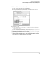
Set up the logic analyzer
1 Set up the Sampling tab.
a
b
c
d
e
84
In the Analyzer setup window, select the Sampling tab.
Select Timing Mode.
In Timing Mode Controls, select Trigger Position and choose Start.
Select the Acquisition Depth field, then choose “256K”.
Select the sample period field. Then enter 3.0 ns.
Chapter 3: Testing Performance
To Test the Time Interval Accuracy
2 Set up the Format tab.
a In the Analyzer setup window, select the Format tab.
b Under the Format tab, select Pod Assignment.
c In the Pod Assignment window, highlight and drag Pods 1 and 2 to the Analyzer 1
column. Highlight and drag pods 3 and 4 to the Unassigned column.
d Select Close to close the Pod Assignment window.
e Under the Format tab, select the field showing the channel assignments for Pod 1.
Clear the channels (all “.”), then select channel 0. An asterisk means that the channel
is turned on.
f Under the Pod 1 field, select TTL, then choose ECL.
85
Chapter 3: Testing Performance
To Test the Time Interval Accuracy
3 Set up the Waveform window.
a In the Analyzer setup window, select Window, then choose Slot n: Analyzer<n>
(where “n” is the slot you have the module installed), then select Waveform. A
Waveform window opens.
b In the Waveform window select the Markers tab.
c Select the G1 field and a Marker Setup window appears.
d Ensure that the Interval Time field reads “from G1 to G2” (instead of “from G2 to
G1”).
Leave this window open as you will be using it later when acquiring data.
86
Chapter 3: Testing Performance
To Test the Time Interval Accuracy
Connect the logic analyzer
1 Using a 6-by-2 test connector, connect channel 0 of Pod 1 to the pulse generator
channel 2 output.
2 Using the SMA cable and the BNC adapter, connect the External Input of the
pulse generator to the Main Signal of the function generator.
Acquire the data
1 Enable the pulse generator channel 2 and trigger outputs (with the LED off).
2 In the logic analyzer Waveform window, select the Run icon.
3 Configure the Markers to measure the time interval.
a In the Marker Setup window select the Time field associated with G1, and choose
Pattern. Select the Time field associated with G2, and choose Pattern.
b Select the Occurs field associated with G1 and enter “1”. Select the Occurs field
associated with G2 and enter “30000”.
87
Chapter 3: Testing Performance
To Test the Time Interval Accuracy
c
Select the From field associated with G2 and select G1.
In the Marker Setup Window, you will observe the Interval Time from G1 to G2=value
to determine the pass or fail status of this test.
d In the marker Setup window, select the Define... field associated with G1, and the G1
Marker Pattern window appears. In the Pattern field, enter “1”.
Select the Pattern Qualify field and select When Entering.
If the Label selection field reads Label1_TZ, you must select Label1 for the search
term. To do this, select Label1_TZ; then, in the popup menu, select Replace label. In
the Replace popup menu, select Label1, then Apply, then Close.
In the Marker Pattern window, select Apply, then select Close.
e In the marker Setup window, select the Define... field associated with G2, and the G2
Marker Pattern window appears. In the Pattern field, enter “1”.
Select the Pattern Qualify field and select When Entering.
If the Label selection field reads Label1_TZ, you must select Label1 for the search
term. Follow the same procedure as in d above.
4 Acquire the data.
a In the Waveform window, select the Run Repetitive icon.
The logic analyzer repetitively acquires data.
88
Chapter 3: Testing Performance
To Test the Time Interval Accuracy
b Continuously observe the Interval Time from G1 to G2=value in the Marker Setup
window.
Allow the logic analyzer to run repetitively for approximately one minute. If the
Interval Time value remains inside the range 749.921 µs to 750.079 µs, the test passes.
Record a Pass or Fail in the performance test record.
c
Select the Stop icon to end the acquisition.
89
Chapter 3: Testing Performance
To Test the Multi-card Module
To Test the Multi-card Module
The multi-card test is only required for configured multi-card modules.
Performing the test verifies the performance of the following specifications:
•
Minimum master to master clock time
•
Maximum state acquisition speed
•
Setup/Hold time
Multi-card modules that were changed to one-card modules for the previous
performance tests need to be reconfigured as a multi-card module for this test.
This test checks a combination of data channels using a single-edge clock at one
selected setup/hold time.
Equipment Required
(TXLSPHQW
&ULWLFDO6SHFLILFDWLRQV
3XOVH*HQHUDWRU
'LJLWL]LQJ2VFLOORVFRSH
$GDSWHU
60$&RD[&DEOH4W\
&RXSOHU4W\
%1&7HVW&RQQHFWRU[4W\
0K]QVSXOVHZLGWKSVULVHWLPH
≥*+]EDQGZLGWKSVULVHWLPH
60$P%1&I
%1&PP
5HFRPPHQGHG0RGHO
3DUW
$RSWLRQ
$Z$
Set up the equipment
If you have not already done so, do the procedure “To Set up the Test Equipment
and the Analyzer” on page 37. Ensure that the pulse generator and oscilloscope
are set up according to the tables in that section.
Set up the logic analyzer
1 Set up the Sampling tab.
a In the Analyzer setup window, select the Sampling tab.
b Select State Mode.
90
Chapter 3: Testing Performance
To Test the Multi-card Module
2 Assign pods 1 and 2 of the master card and all expander cards to Analyzer 1.
a In the Analyzer setup window, select the Format tab.
b Under the Format tab, select Pod Assignment.
c In the pod Assignment window, highlight and drag the pods 1 and 2 to the Analyzer 1
column. Highlight and drag pods 3 and 4 to the Unassigned Pods column.
d Select Close to close the pod assignment window.
3 Set up the Format tab.
a Under one of the pod fields, select TTL.
b In the Pod Threshold window, select ECL.
c In the Pod Threshold window, ensure the Apply threshold settings to all pods
checkbox is checked.
d Select Close to close the Pod Threshold window.
91
Chapter 3: Testing Performance
To Test the Multi-card Module
4 Set up the Trigger tab.
a In the Analyzer setup window, select the Trigger tab. Under the Trigger tab, select the
Settings tab.
b Select the Acquisition Depth field, then choose “8K”.
c Select the Count field, then choose “Off”.
d Select the Trigger Position field, then choose Start.
5 Set up the Listing window.
a In the Listing window, select the Markers tab.
b Select the G1: field and the Markers Setup window appears.
c Select the Time field associated with G1, and select Pattern. Select the Time field
associated with G2, and choose Pattern.
Note: Leave the Marker Setup window open. You will be entering numeric values
in the “occurs” field after acquiring the test data.
92
Chapter 3: Testing Performance
To Test the Multi-card Module
Connect the logic analyzer
1 Using the 6-by-2 test connectors, connect the logic analyzer clock and data
channels listed in the following tables to the pulse generator.
2 Using SMA cables, connect channel 1, channel 2, and trigger from the
oscilloscope to the pulse generator according to the following illustration.
Connect the Logic Analyzer to the Pulse Generator (2-, 3-, and 4-card module)
0DVWHU%RDUG
$OO([SDQGHU%RDUGV
&RQQHFWWR$
&KDQQHO2XWSXW
&RQQHFWWR$
&KDQQHO2XWSXW
&RQQHFWWR$
&KDQQHO2XWSXW
3RGFKDQQHO
3RGFKDQQHO
3RGFKDQQHO
3RGFKDQQHO
-FORFN
Connect the Logic Analyzer to the Pulse Generator (5-card module)
&RQQHFWWR$
&KDQQHO2XWSXW
&RQQHFWWR$
&KDQQHO2XWSXW
&RQQHFWWR$
&KDQQHO2XWSXW
0DVWHU%RDUG
-FORFN
$OO([SDQGHU%RDUGV
3RGFKDQQHO
3RGFKDQQHO
)RUDFDUGPRGXOHGRQRWFRQQHFWWKHPDVWHUERDUGWRWKHFKDQQHORXWSXWDQG
RXWSXW&RQQHFWRQO\WKHIRXUH[SDQGHUERDUGV
3 Activate the data channels that are connected according to the previous table.
a In the Analyzer setup window, select the Format tab.
93
Chapter 3: Testing Performance
To Test the Multi-card Module
b Under the Format tab, select the field showing the channel assignments for Pod 1 of
one of the Expander cards.
c Select Individual, then choose channels 3 and 11. An asterisk means that a channel is
turned on. Follow this step for the Pod 1 of each of the remaining Expander cards and
for the Master card (if a 5-card module is not being tested).
4 Configure the trigger pattern
a Select the Trigger tab. Under the Trigger tab, select the Trigger Functions tab.
b In the General State field, select Store nothing until pattern occurs. Then select
Replace.
c Under Trigger Sequence, locate the Label 1 = trigger pattern field. Enter the pattern
according to the following table.
2-card module: “A”
3-card module: “2A”
4-card module: “AA”
94
Chapter 3: Testing Performance
To Test the Multi-card Module
5-card module: “AA”
95
Chapter 3: Testing Performance
To Test the Multi-card Module
Verify the test signal
1 Check the clock period. Using the oscilloscope, verify that the master-to-master
clock time is 5.988 ns, +0 ps or -100 ps.
a Turn on the pulse generator channel 1, channel 2, and trigger outputs.
b In the oscilloscope Timebase menu, select Scale: 1.000 ns/div.
c In the oscilloscope Timebase menu, select Position. Using the oscilloscope knob,
position the clock waveform so that a rising edge appears at the left of the display.
d On the oscilloscope, select [Shift] Period: channel 2, then select [Enter] to display the
clock period (Period(2)). If the period is more than 5.988 ns, go to step e. If the
period is less than or equal to 5.988 ns but greater than 5.888 ns, go to step 2.
e In the oscilloscope Timebase menu, increase Position 5.988 ns. If the period is more
than 5.988 ns, decrease the pulse generator Period in 10 ps increments until one of
the two periods measured is less than or equal to 5.988 ns but greater than 5.888 ns.
Data Signal
Clock Signal
Clock Period
96
Chapter 3: Testing Performance
To Test the Multi-card Module
2 Check the data pulse width. Using the oscilloscope, verify that the data pulse
width is -2.500 ns, +0 ps or -50 ps.
a In the oscilloscope Timebase menu, select Scale: 1.000 ns/div.
b In the oscilloscope Timebase menu, select Position. Using the oscilloscope knob,
position the data waveform so that the waveform is centered on the screen.
c On the oscilloscope, select [Shift] + width: channel 1, then select [Enter] to display the
data signal pulse width (+ width(1)).
d If the pulse width is outside the limits, adjust the pulse generator channel 2 width
until the pulse width is within limits.
Data Signal
Clock Signal
Data Pulse
Width
97
Chapter 3: Testing Performance
To Test the Multi-card Module
Check the setup/hold combination
1 Select the logic analyzer setup/hold time.
a
b
c
d
In the Analyzer setup window, select the Format tab.
Under the Format tab, select Setup/Hold.
In the Setup and Hold window, ensure All bits is selected.
Enter 4.500 ns in the Setup: field.
e Select the close (X) button in the upper-right corner to close the Setup/Hold window.
2 Disable the pulse generator channel 1 COMP (LED off).
3 Using the Delay mode of the pulse generator channel 1, position the pulses
according to the setup/hold combination selected, +0.0 ps or -50 ps.
a On the Oscilloscope, select [Define meas] Define ∆Time - Stop edge: rising.
b In the oscilloscope timebase menu, select Position. Using the oscilloscope knob,
position both a clock and a data waveform on the display, with the rising edge of the
clock waveform centered on the display.
c On the oscilloscope, select [Shift] ∆ Time, then select [Enter] to display the setup time
(∆Time(1)-(2)).
98
Chapter 3: Testing Performance
To Test the Multi-card Module
d Adjust the pulse generator channel 1 Delay until the pulses are aligned for a setup
time of 4.500 ns, +0.0 ps or -50 ps.
Data Signal
Clock Signal
Setup Time
4 Select the clock to be tested.
a In the Analyzer setup window select the Sampling tab.
b Under the Sampling tab, select the clock edge field under the clock to be tested. Then
select Rising Edge.
Clocks
-↑
c
.↑
/↑
0↑
Connect the clock input channel to be tested to the pulse generator channel 1
OUTPUT. Disconnect all other clock input channels.
99
Chapter 3: Testing Performance
To Test the Multi-card Module
5 Verify the test data.
a In the Listing window, select the Run icon. The display should show an alternating
pattern of
“A” and “5” (2-card module)
“2A” and “15” (3-card module)
“AA” and “55” (4- or 5-card module).
b In the Marker Setup window, select the Define... field associated with G1, and the G1
Marker Pattern window appears. In the pattern field, enter
“A” (2-card module)
“2A” (3-card module) or
“AA” (4- or 5-card module).
Select Apply, then select Close.
If the Label selection field reads Label1_TZ, your must select Label1 for the search
term. To do this, select Labe1_TZ; then, in the popup menu, select Replace label. In
the Replace popup menu, select Label1, then Apply, then Close.
c
In the Marker Setup window, select the Define... field associated with G2, and the G2
Marker Pattern window appears. In the pattern field, enter
“5” (2-card module)
“15” (3-card module) or
100
Chapter 3: Testing Performance
To Test the Multi-card Module
“55” (4- or 5-card module).
Select Apply, then select Close.
If the Label selection field reads Label1_TZ, you must select Label1 for the search
term. Follow the same procedure as in b above.
d In the Marker Setup window, select the ‘occurs’ value field that corresponds to marker
G1. Enter 4095.
e In the Marker Setup window, select the ‘occurs’ value field that corresponds to marker
G2. Enter 4096.
f
Select Close to apply the marker values to the data. If the “Pattern NOT found for
marker…” error message does not appear, then the test passes. Record the Pass or
Fail in the performance test record.
6 Repeat steps 4 and 5 for the next clock edge listed in the table in step 4, until all
listed clock edges have been tested.
101
Chapter 3: Testing Performance
To Test the 333 MHz State Mode (16717/18/19A)
To Test the 333 MHz State Mode (16717/18/19A)
The 333 MHz State Mode test is only required for the 16717/18/19A. Performing
the test verifies the performance of the following specifications:
•
Minimum master to master clock time
•
Maximum state acquisition speed
This test is done on either a single-card or a multi-card module.
This test checks a combination of data channels using a double-edge clock at one
selected setup/hold time.
Equipment Required
(TXLSPHQW
&ULWLFDO6SHFLILFDWLRQV
3XOVH*HQHUDWRU
'LJLWL]LQJ2VFLOORVFRSH
$GDSWHU
60$&RD[&DEOH4W\
&RXSOHU4W\
%1&7HVW&RQQHFWRU[4W\
0K]QVSXOVHZLGWKSVULVHWLPH
≥*+]EDQGZLGWKSVULVHWLPH
60$P%1&I
%1&PP
5HFRPPHQGHG0RGHO
3DUW
$RSWLRQ
$Z$
Set up the equipment
1 If you have not already done so, do the procedure “To Set up the Test Equipment
and the Analyzer” on page 37. Ensure that the pulse generator and oscilloscope
are set up according to the tables in that section.
2 Change the pulse generator Period to 6.006 ns.
Set up the logic analyzer
1 Set up the Sampling tab.
a In the Analyzer setup window, select the Sampling tab.
b Select State Mode.
c Under State Mode Controls, select 167MHz/nnM state (where “nn” is the memory
depth of the logic analyzer module being tested).
d In the pop-up menu, select 333MHz/nnM state.
102
Chapter 3: Testing Performance
To Test the 333 MHz State Mode (16717/18/19A)
2 Make the following changes to the pulse generator configuration.
7LPHEDVH
&KDQQHO
3HULRGQV
0RGHVTXDUH
3 Assign pods 1 and 2 of the master card and all expander cards to Analyzer 1.
a In the Analyzer setup window, select the Format tab.
b Under the Format tab, select Pod Assignment.
c In the Pod Assignment window, highlight and drag the pods 1 and 2 to the Analyzer 1
column. Highlight and drag pods 3 and 4 to the Unassigned Pods column.
d Select Close to close the pod assignment window.
4 Set up the Format tab.
a Under one of the pod fields, select TTL.
b In the Pod Threshold window, select ECL.
c In the Pod Threshold window, ensure the Apply threshold settings to all pods
checkbox is checked.
103
Chapter 3: Testing Performance
To Test the 333 MHz State Mode (16717/18/19A)
d Select Close to close the Pod Threshold window.
5 Set up the Trigger tab.
a In the Analyzer setup window, select the Trigger tab. Under the Trigger tab, select the
Settings tab.
b Select the Acquisition Depth field, then choose “8K”.
c Select the Trigger Position field, then choose Start.
6 Set up the Listing window.
a In the Listing window, select the Markers tab.
b Select the G1: field and the Markers Setup window appears.
c Select the Time field associated with G1, and select Pattern. Select the Time field
associated with G2, and select Pattern.
d Select the Trigger field associated with G1, and select Beginning. Select the Trigger
field associated with G2, and choose Beginning.
Note: Leave the Marker Setup window open. You will be entering numeric values
in the “occurs” field after acquiring the test data.
104
Chapter 3: Testing Performance
To Test the 333 MHz State Mode (16717/18/19A)
Connect the logic analyzer
1 Using the 6-by-2 test connectors, connect the logic analyzer clock and data
channels listed in the following tables to the pulse generator.
2 Using SMA cables, connect channel 1, channel 2, and trigger from the
oscilloscope to the pulse generator according to the following illustration.
Connect the Logic Analyzer to the Pulse Generator (1-Card Module)
&RQQHFWWR$
&KDQQHO2XWSXW
&RQQHFWWR$
&KDQQHO2XWSXW
&RQQHFWWR$&KDQQHO
2XWSXW
3RGFKDQQHO
3RGFKDQQHO
-FORFN
Connect the Logic Analyzer to the Pulse Generator (2-, 3-, and 4-card module)
0DVWHU%RDUG
$OO([SDQGHU%RDUGV
&RQQHFWWR$
&KDQQHO2XWSXW
&RQQHFWWR$
&KDQQHO2XWSXW
&RQQHFWWR$
&KDQQHO2XWSXW
3RGFKDQQHO
3RGFKDQQHO
3RGFKDQQHO
3RGFKDQQHO
-FORFN
105
Chapter 3: Testing Performance
To Test the 333 MHz State Mode (16717/18/19A)
Connect the Logic Analyzer to the Pulse Generator (5-card module)
0DVWHU%RDUG
$OO([SDQGHU%RDUGV
&RQQHFWWR$
&KDQQHO2XWSXW
&RQQHFWWR$
&KDQQHO2XWSXW
3RGFKDQQHO
3RGFKDQQHO
&RQQHFWWR$
&KDQQHO2XWSXW
-FORFN
)RUDFDUGPRGXOHGRQRWFRQQHFWWKHPDVWHUERDUGWRWKHFKDQQHORXWSXWDQGRXWSXW&RQQHFWRQO\
WKHIRXUH[SDQGHUERDUGV
3 Activate the data channels that are connected according to the previous table.
a In the Analyzer setup window, select the Format tab.
b Under the Format tab, select the field showing the channel assignments for Pod 1 of
one of the Expander cards.
c Select Individual, then choose channels 3 and 11. An asterisk means that a channel is
turned on. Follow this step for the Pod 1 of each of the remaining Expander cards.
4 Configure the trigger patern.
a Select the Trigger tab. Under the Trigger tab, select the Trigger Functions tab.
b In the General State field, select [Find pattern n times]. Then select Replace.
106
Chapter 3: Testing Performance
To Test the 333 MHz State Mode (16717/18/19A)
c
Under Trigger Sequence, locate the Label 1 = trigger pattern field. Enter the pattern
according to the following table:
1-card module: “2”
2-card module: “A”
3-card module: “2A”
4-card module: “AA”
5-card module: “AA”
107
Chapter 3: Testing Performance
To Test the 333 MHz State Mode (16717/18/19A)
Verify the test signal
1 Check the clock interval. Using the oscilloscope, verify that the master-tomaster clock time is 3.003 ns, +0 ps or -50 ps.
a Turn on the pulse generator channel 1, channel 2, and trigger outputs.
b In the oscilloscope Timebase menu, select Scale: 1.000 ns/div.
c In the oscilloscope Timebase menu, select Position. Using the oscilloscope knob,
position the clock waveform so that a rising edge appears at the left of the display.
d On the oscilloscope, select [Shift] + width: channel 2. Then select [Enter] to display
the master-to-master clock time (+ width(2)). If the positive-going pulse width is
more than 3.003 ns, go to stop e. If the positive-going pulse width is less than or equal
to 3.003 ns but greater than 2.953 ns, check the setup/hold combination.
e On the oscilloscope, select [Shift] - width: channel 2, then select [Enter](- width(2)).
If the negative pulse width is less than or equal to 3.003 ns but greater than 2.953 ns,
check the setup/hold combination
f Decrease the pulse generator Period in 10-ps increments until the oscilloscope +
width (2) or - width (2) read less than or equal to 3.003 ns, but greater than 2.953 ns.
Data Signal
Clock Signal
Clock Period
108
Chapter 3: Testing Performance
To Test the 333 MHz State Mode (16717/18/19A)
Check the setup/hold combination
1 Select the logic analyzer setup/hold time.
a In the Analyzer setup window, select the Sampling tab. Under the Sampling tab, select
the J clock edge field, then choose Both Edges.
b Select the Format tab. Under the Format tab, select Setup/Hold.
c In the Setup and Hold window, ensure All bits is selected.
d In the Setup and Hold window, enter 3.000 ns in the Setup: field.
e Select the close (X) button in the upper-right corner to close the Setup/Hold window.
2 Using the Delay mode of the pulse generator channel 1, position the pulses
according to the setup/hold combination selected, +0.0 ps or -50 ps.
a On the Oscilloscope, select [Define meas] Define ∆Time - Stop edge: rising.
b In the oscilloscope timebase menu, select Position. Using the oscilloscope knob,
position both a clock and a data waveform on the display, with the rising edge of the
clock waveform centered on the display.
c On the oscilloscope, select [Shift] ∆ Time, then select [Enter] to display the setup time
(∆Time(1)-(2)).
109
Chapter 3: Testing Performance
To Test the 333 MHz State Mode (16717/18/19A)
d Adjust the pulse generator channel 1 Delay until the pulses are aligned according the
setup time of the setup/hold combination selected, +0.0 ps or -100 ps.
Data Signal
Clock Signal
Setup Time
110
Chapter 3: Testing Performance
To Test the 333 MHz State Mode (16717/18/19A)
3 Verify the test data.
a In the Listing window, select the Run icon. The display should show an alternating
pattern of:
“2” and “1” (1-card module)
“A” and “5” (2-card module)
“2A” and “15” (3-card module)
“AA” and “55” (4- or 5-card module)
b In the Marker Setup window, select the Define... field associated with G1, and the G1
Marker Pattern window appears. In the pattern field, enter
“2” (1-card module)
“A” (2-card module)
“2A” (3-card module)
“AA” (4- or 5-card module)
Select Apply, then select Close.
If the Label selection field reads Label1_TZ, you must select Label1 for the search
term. To do this, select Label1_TZ; then, in the popup menu, select Replace label. In
the Replace popup menu, select Label1, then Apply, then Close.
111
Chapter 3: Testing Performance
To Test the 333 MHz State Mode (16717/18/19A)
c
In the Marker Setup window, select the Define... field associated with G2, and the G2
Marker Pattern window appears. In the pattern field, enter
“1” (1-card module)
“5” (2-card module)
“15” (3-card module)
“55” (4- or 5-card module)
Select Apply, then select Close.
If the Label selection field reads Label1_TZ, you must select Label1 for the search
term. Follow the same procedure as in b above.
d In the Marker Setup window, select the ‘occurs’ value field that corresponds to marker
G1. Enter 4095.
e In the Marker Setup window, select the ‘occurs’ value field that corresponds to marker
G2. Enter 4096.
f
112
Select Close to apply the marker values to the data. If the “Pattern NOT found for
marker…” error message does not appear, then the test passes. Record the Pass or
Fail in the performance test record.
Chapter 3: Testing Performance
Performance Test Record
Performance Test Record
Performance Test Record
$/RJLF$QDO\]HU
6HULDO1RBBBBBBBBBBBBBBBBBBBBBBBB
5HFRPPHQGHG7HVW,QWHUYDO<HDUKRXUV
5HFRPPHQGHGQH[WWHVWLQJBBBBBBBBBBBBBBB
7HVW
6HWWLQJV
5HVXOWV
3DVV)DLO
________
(&/9/
(&/9+
98VHU9/
98VHU9+
/LPLWV
²9
²9
²P9
P9
0HDVXUHG
________
________
________
________
(&/9/
(&/9+
98VHU9/
98VHU9+
²9
²9
²P9
P9
________
________
________
________
(&/9/
(&/9+
98VHU9/
98VHU9+
²9
²9
²P9
P9
________
________
________
________
(&/9/
(&/9+
98VHU9/
98VHU9+
²9
²9
²P9
P9
________
________
________
________
6HOI7HVWV
7KUHVKROG
$FFXUDF\
:RUN2UGHU1RBBBBBBBBBBBBBBBBBBB
'DWHBBBBBBBBBBBBBBBBBBBBBBBBBBBB
7HPSHUDWXUHBBBBBBBBBBBBBBBBBBBBBB
P9RIWKUHVKROGVHWWLQJ
3RG
(&/P9
9P9
3RG
(&/P9
9P9
3RG
(&/P9
9P9
3RG
(&/P9
9P9
113
Chapter 3: Testing Performance
Performance Test Record
7HVW
6HWWLQJV
5HVXOWV
3DVV)DLO
6LQJOH&ORFN6LQJOH(GJH$FTXLVLWLRQ
$OO3RGV
6HWXS+ROG7LPH
6HWXS+ROG7LPH
114
QV
QV
-↑
.↑
/↑
0↑
BBBBBBBB
BBBBBBBB
BBBBBBBB
BBBBBBBB
-↓
.↓
/↓
0↓
BBBBBBBB
BBBBBBBB
BBBBBBBB
BBBBBBBB
-↑
.↑
/↑
0↑
BBBBBBBB
BBBBBBBB
BBBBBBBB
BBBBBBBB
-↓
.↓
/↓
0↓
BBBBBBBB
BBBBBBBB
BBBBBBBB
BBBBBBBB
Chapter 3: Testing Performance
Performance Test Record
7HVW
6HWWLQJV
5HVXOWV
3DVV)DLO
0XOWLSOHFORFN0XOWLSOHHGJHDFTXLVLWLRQ
$OO3RGV
6HWXS+ROG7LPH
QV
-↑.↑/↑ + 0↑
________
-↓.↓/↓0↓
________
6HWXS+ROG7LPH
QV
-↑.↑/↑0↑
________
-↓.↓/↓0↓
________
3DVV)DLO
6LQJOH&ORFN0XOWLSOH(GJH$FTXLVLWLRQ
$OO3RGV
3DVV)DLO
6HWXS+ROG7LPH
QV
-↕
.↕
/↕
0↕
________
________
________
________
6HWXS+ROG7LPH
QV
-↕
.↕
/↕
0↕
________
________
________
________
7LPH,QWHUYDO$FFXUDF\
,QWHUYDOWLPHIURP
*WR*
3DVV)DLO
µV
BBBBBBBB
0XOWL&DUG7HVW
6HWXS+ROG7LPH
QV
-↑
.↑
/↑
0↑
3DVV)DLO
BBBBBBBB
BBBBBBBB
BBBBBBBB
BBBBBBBB
3DVV)DLO
QV
-↕
BBBBBBBB
0+]6WDWH0RGH7HVW
6HWXS+ROG7LPH
115
Chapter 3: Testing Performance
Performance Test Record
116
4
Calibrating
This chapter gives you instructions for calibrating the logic analyzer.
Chapter 4: Calibrating
Calibration Strategy
The 16715/16/17/18/19A logic analyzer does not require an operational accuracy
calibration. To test the module against the module specifications, refer to
"Testing Performance" in chapter 3.
118
5
"To use the flowcharts" on page 120
"To run the self-tests" on page 123
"To exit the test system" on page 124
"To test the cables" on page 125
"To test the auxiliary power" on page 129
Troubleshooting
This chapter helps you troubleshoot the module to find defective assemblies.
Chapter 5: Troubleshooting
To use the flowcharts
The troubleshooting section consists of flowcharts, self-test instructions, a cable
test, and a test for the auxiliary power supplied by the probe cable.
If you suspect a problem, start at the top of the first flowchart. During the
troubleshooting instructions, the flowcharts will direct you to perform the selftests or the cable test.
The service strategy for this instrument is the replacement of defective
assemblies. This module can be returned to Agilent Technologies for all service
work, including troubleshooting. Contact your nearest Agilent Technologies Sales
Office for more details.
CAUTION
(OHFWURVWDWLFGLVFKDUJHFDQGDPDJHHOHFWURQLFFRPSRQHQWV8VHJURXQGHGZULVWVWUDSV
DQGPDWVZKHQ\RXSHUIRUPDQ\VHUYLFHWRWKLVLQVWUXPHQWRUWRWKHFDUGVLQLW
To use the flowcharts
Flowcharts are the primary tool used to isolate defective assemblies. The flowcharts refer
to other tests to help isolate the trouble. The circled numbers on the charts indicate
connections with the other flowcharts. Start your troubleshooting at the top of the first
flowchart.
Mainframe Operating System
Before starting the troubleshooting on an 16715/16/17/18/19A, ensure that the required
version of 16700-series mainframe operating system is installed on the mainframe. The
required operating system software versions are listed in "Mainframe and Operating
System" on page 10. To check the operating system version number, open the System
Administration window, select the Admin tab, then choose About...
If the proper version is not loaded, obtain a copy of the updated operating system
software and install it in the logic analyzer.
120
Chapter 5: Troubleshooting
To use the flowcharts
Troubleshooting Flowchart 1
121
Chapter 5: Troubleshooting
To use the flowcharts
Troubleshooting Flowchart 2
122
Chapter 5: Troubleshooting
To run the self-tests
To run the self-tests
Self-tests identify the correct operation of major, functional subsystems of the module.
You can run all self-tests without accessing the module. If a self-test fails, the
troubleshooting flowcharts instruct you to change a part of the module.
To run the self-tests:
1 In the System window, select System Admin.
2 In the System Administration window, select the Admin tab, then choose SelfTest. At the Test Query window, select Yes.
The tests can be run individually, or all the tests can be run by selecting Test All at the
bottom of the Self Test window. Note that if Test All is selected, system tests requiring
user action will not be run. For more information, refer to Chapter 8 in the mainframe
service manual.
3 In the Self Test window under the System tab, select System CPU Board.
4 Run the floppy drive test.
a In the Self Test: System CPU Board window, select Floppy Drive Test.
b Insert a DOS-formatted disk with 300KB of available space in the mainframe floppy
drive.
c In the Test Query window, select OK.
The Test Query window instructs you to insert the disk into the disk drive. The other
System CPU Board tests require similar user action to successfully run the test.
5 In the Self Test: System CPU Board window, select Close to close the window.
6 In the Self Test window, select PCI Board. Select Test All to run all PCI board
tests.
7 In the Self Test window, select the Master Frame tab. Select the 16715/16/17/18/
19A module to be tested, then select Test All to run all the module tests. The
module test status should indicate PASSED (see screen on next page).
123
Chapter 5: Troubleshooting
To exit the test system
Refer to Chapter 8 in the mainframe service manual for more information on system tests
that are not executed.
To exit the test system
To exit the test system
1 Select Close to close any module or system test windows.
2 In the Self Test window, select Quit.
3 In the session manager window, select Start Session to launch a new logic
analyzer session.
124
Chapter 5: Troubleshooting
To test the cables
To test the cables
This test allows you to functionally verify the probe cable and probe tip assembly of any
of the logic analyzer pods. Only one probe cable can be tested at a time. Repeat this test
for each probe cable to be tested.
Equipment Required
(TXLSPHQW
&ULWLFDO6SHFLILFDWLRQ
3XOVH*HQHUDWRU
0+]QVSXOVHZLGWK
SVULVHWLPH
5HFRPPHQGHG0RGHO
3DUW
$2SWLRQ
[7HVW&RQQHFWRUV4W\
1 If you have not already done so, do the procedure ""To Set up the Test
Equipment and the Analyzer" on page 37 in Chapter 3.
2 Set up the pulse generator.
a Set up the pulse generator according to the following table
Pulse Generator Setup
7LPHEDVH
&KDQQHO
&KDQQHO
7ULJJHU
0RGH,QW
3HULRGQV
0RGH6TXDUH
'HOD\QV
+LJK9
/RZ9
&203'LVDEOHG
/('2II
0RGH6TXDUH
'HOD\QV
+LJK9
/RZ9
&203'LVDEOHG
/('2II
'LYLGH'LYLGH÷ $PSO9
2IIV9
b Enable the pulse generator channel 1 and channel 2 outputs (LED off).
3 Set up the Sampling tab.
a In the Analyzer setup window, select the Sampling tab.
b Select State Mode.
c Select Master Clock. In the Master Clock window, select both edges for the J clock
(J↕). Turn off the other clocks.
125
Chapter 5: Troubleshooting
To test the cables
d Select Acquisition Depth field, then choose 8K.
4 Assign all pods to Analyzer 1, and configure the pod under test.
a Select the Format tab. Under the Format tab, select Pod Assignment.
b Highlight and drag the pods to the Analyzer 1 column.
c
126
Select the field showing the channel assignments for the pod under test. In the pop-up
menu, select the asterisk field to put asterisks in the channel positions, activating the
channels. Select Done.
Chapter 5: Troubleshooting
To test the cables
d Select Setup and Hold, then enter 3.000 ns in the Setup: field. Select OK to close the
Setup and Hold window.
e Select the close (X) button in the upper-right corner to close the Setup/Hold window.
f Ensure the threshold is set to TTL. If not, select the threshold field, then select TTL.
5 Set up the Listing window.
a In the Analyzer Setup window, select Window, then choose Slot n: Analyzer (where
“n” is the slot the module under test is installed), then select Listing. A Listing window
opens.
b Select the Hex field and change the Lab1 base to Binary.
6 Using four 6-by-2 test connectors, connect the logic analyzer to the pulse
generator channel outputs. To make the test connectors, see chapter 3, "Testing
Performance."
a Connect the even-numbered channels of the lower byte of the pod under test to the
pulse generator channel 1 Output.
b Connect the odd-numbered channels of the lower byte of the pod under test to the
pulse generator channel 1 Output.
c Connect the even-numbered channels of the upper byte of the pod under test and the
J clock channel to the pulse generator channel 2 Output. J clock is located on Pod 1.
d Connect the odd-numbered channels of the upper byte of the pod under test to the
pulse generator channel 2 Output.
127
Chapter 5: Troubleshooting
To test the cables
7 On the logic analyzer, select the Run icon. The listing should look similar to the
figure below. Ignore any error messages dealing with the G1 and G2 markers.
8 If the listing looks like the figure, then the cable passed the test.
If the listing does not look similar to the figure, then there is a possible problem with the
cable or probe tip assembly. Causes for cable test failures include:
•
open channel.
•
channel shorted to a neighboring channel.
•
channel shorted to either ground or a supply voltage.
Return to the troubleshooting flowchart.
128
Chapter 5: Troubleshooting
To test the auxiliary power
To test the auxiliary power
The +5 V auxiliary power is protected by a current overload protection circuit. If the
current on pins 1 and 39 exceeds 0.33 amps, the circuit will open. When the short is
removed, the circuit will reset in approximately 1 minute. There should be +5 V after the
1 minute reset time.
Equipment Required
•
(TXLSPHQW
&ULWLFDO6SHFLILFDWLRQV
5HFRPPHQGHG0RGHO
3DUW
'LJLWDO0XOWLPHWHU
QD
($
Using the multimeter, verify the +5 V on pins 1 and 39 of the probe cables.
129
130
6
To remove the module 133
To replace the circuit board 134
To replace the module 135
To replace the probe cable 137
To return assemblies 138
Replacing Assemblies
This chapter contains the instructions for removing and replacing the logic
analyzer module, the circuit board of the module, and the probe cables of the
module as well as the instructions for returning assemblies.
Chapter 6: Replacing Assemblies
CAUTION
7XUQRIIWKHLQVWUXPHQWEHIRUHLQVWDOOLQJUHPRYLQJRUUHSODFLQJDPRGXOHLQWKH
LQVWUXPHQW
Tools Required
•
A T10 TORX screwdriver, to remove screws connecting the probe cables and screws
connecting the back panel.
•
A 1/4-inch hollow-shaft nutdriver, to remove the nut holding the cable to the module
panel insert.
132
Chapter 6: Replacing Assemblies
To remove the module
To remove the module
CAUTION
(OHFWURVWDWLFGLVFKDUJHFDQGDPDJHHOHFWURQLFFRPSRQHQWV8VHJURXQGHGZULVWVWUDSV
DQGPDWVZKHQSHUIRUPLQJDQ\VHUYLFHWRWKLVPRGXOH
1 Remove power from the instrument.
a
b
c
d
Exit all logic analysis sessions. In the session manager, select Shutdown.
At the query, select Power Down.
When the “OK to power down” message appears, turn the instrument off.
Disconnect the power cord.
2 Loosen the thumb screws.
Starting from the top, loosen the thumb screws on the filler panels and cards located
above the module and the thumb screws of the module.
3 Starting from the top, pull the cards and filler panels located above the module
half-way out.
4 If the module consists of a single card, pull the card completely out.
If the module consists of multiple cards, pull all cards completely out.
5 Push all other cards into the card cage, but not completely in.
This is to get them out of the way for removing and replacing the module.
6 If the module consist of a single card, replace the faulty card.
If the module consists of multiple cards, remove the 2x40 cables from the top multicard
connector of all cards. Remove the 2x10 cables from J4, J5, J7, and J8 from the master
card. Remove the faulty card from the module.
133
Chapter 6: Replacing Assemblies
To replace the circuit board
To replace the circuit board
1 Remove the three screws connecting the probe cables to the back panel, then
disconnect the probe cables.
2 Remove the four screws attaching the ground spring and back panel to the
circuit board, then remove the back panel and the ground spring.
3 Replace the faulty circuit board with a new circuit board. On the faulty board,
make sure the 20-pin ribbon cable is connected between J3 and J6.
4 Position the ground spring and back panel on the back edge of the replacement
circuit board. Install four screws to connect the back panel and ground spring to
the circuit board.
5 Connect the probe cables, then install three screws to connect the cables to the
back panel.
CAUTION
,I\RXRYHUWLJKWHQWKHVFUHZVWKHWKUHDGHGLQVHUWVRQWKHEDFNSDQHOPLJKWEUHDNRIIRI
WKHEDFNSDQHO7LJKWHQWKHVFUHZVRQO\HQRXJKWRKROGWKHFDEOHLQSODFH
134
Chapter 6: Replacing Assemblies
To replace the module
To replace the module
1 If the module consists of one card, go to step 2.
If the module consists of more than one card, connect the cables together in a master/
expander configuration. Follow the procedure "To configure a multicard module" in
chapter 2.
2 Slide the cards above the slots for the module about halfway out of the
mainframe.
3 With the probe cables facing away from the instrument, slide the module
approximately halfway into the mainframe.
4 Slide the complete module into the mainframe, but not completely in.
Each card in the instrument is firmly seated and tightened one at a time in step 6.
135
Chapter 6: Replacing Assemblies
To replace the module
5 Position all cards and filler panels so that the endplates overlap.
6 Seat the cards and tighten the thumbscrews.
Starting with the bottom card, firmly seat the cards into the backplane connector of the
mainframe. Keep applying pressure to the center of the card endplate while tightening
the thumbscrews finger-tight. Repeat this for all cards and filler panels starting at the
bottom and moving to the top.
CAUTION
&RUUHFWDLUFLUFXODWLRQNHHSVWKHLQVWUXPHQWIURPRYHUKHDWLQJ)RUFRUUHFWDLU
FLUFXODWLRQILOOHUSDQHOVPXVWEHLQVWDOOHGLQDOOXQXVHGFDUGVORWV.HHSDQ\H[WUDILOOHU
SDQHOVIRUIXWXUHXVH
136
Chapter 6: Replacing Assemblies
To replace the probe cable
To replace the probe cable
1 Remove power from the instrument.
a
b
c
d
Exit all logic analysis sessions. In the session manager, select Shutdown.
At the query, select Power Down.
When the “OK to power down” message appears, turn the instrument off.
Disconnect the power cord.
2 Remove the screws that hold the probe cable to the rear panel of the module.
3 Remove the faulty probe cable from the connector and install the replacement
cable.
4 Install the label on the new probe.
If you order a new probe cable, you will need to order new labels. Probe cables shipped
with the module are labeled. Probe cables shipped separately are not labeled. Refer to
chapter 7, "Replaceable Parts," for the part numbers and ordering information.
5 Install the screws connecting the probe cable to the rear panel of the module.
CAUTION
,I\RXRYHUWLJKWHQWKHVFUHZVWKHWKUHDGHGLQVHUWVRQWKHEDFNSDQHOPLJKWEUHDNRIIRI
WKHEDFNSDQHO7LJKWHQWKHVFUHZVRQO\HQRXJKWRKROGWKHFDEOHLQSODFH
137
Chapter 6: Replacing Assemblies
To return assemblies
To return assemblies
Before shipping the module to Agilent Technologies, contact your nearest Agilent
Technologies Sales Office for additional details. In the U.S., call 1-800-403-0801.
1 Write the following information on a tag and attach it to the module.
•
Name and address of owner
•
Model number
•
Serial number
•
Description of service required or failure indications
2 Remove accessories from the module.
Only return accessories to Agilent if they are associated with the failure symptoms.
3 Package the module.
You can use either the original shipping containers, or order materials from an Agilent
sales office.
CAUTION
)RUSURWHFWLRQDJDLQVWHOHFWURVWDWLFGLVFKDUJHSDFNDJHWKHPRGXOHLQHOHFWURVWDWLF
PDWHULDO
4 Seal the shipping container securely, and mark it FRAGILE.
138
7
Replaceable Parts Ordering 140
Replaceable Parts List 141
Exploded View 143
Replaceable Parts
This chapter contains information for identifying and ordering replaceable parts
for your module.
Chapter 7: Replaceable Parts
Replaceable Parts Ordering
Replaceable Parts Ordering
Parts listed
To order a part on the list of replaceable parts, quote the part number, indicate the
quantity desired, and address the order to the nearest Agilent Technologies Sales Office.
Parts not listed
To order a part not on the list of replaceable parts, include the model number and serial
number of the module, a description of the part (including its function), and the number
of parts required. Address the order to your nearest Agilent Technologies Sales Office.
Direct mail order system
To order using the direct mail order system, contact your nearest Agilent Technologies
Sales Office.
Within the USA, Agilent can supply parts through a direct mail order system. The
advantages to the system are direct ordering and shipment from the Part Center in
Mountain View, California. There is no maximum or minimum on any mail order. (There is
a minimum amount for parts ordered through a local Agilent Technologies Sales Office
when the orders require billing and invoicing.) Transportation costs are prepaid (there is
a small handling charge for each order) and no invoices.
In order for Agilent to provide these advantages, a check or money order must
accompany each order. Mail order forms and specific ordering information are available
through your local Agilent Technologies Sales Office. Addresses and telephone numbers
are located in a separate document shipped with the 16700-series Logic Analysis
System Service Manual.
Exchange assemblies
Some assemblies are part of an exchange program with Agilent Technologies.
The exchange program allows you to exchange a faulty assembly with one that has been
repaired and performance verified by Agilent Technologies.
After you receive the exchange assembly, return the defective assembly to Agilent
Technologies. A United States customer has 30 days to return the defective assembly. If
you do not return the defective assembly within the 30 days, Agilent Technologies will
charge you an additional amount. This amount is the difference in price between a new
assembly and that of the exchange assembly. For orders not originating in the United
States, contact your nearest Agilent Technologies Sales Office for information.
See Also
To return assemblies 138
140
Chapter 7: Replaceable Parts
Replaceable Parts List
Replaceable Parts List
The replaceable parts list is organized by reference designation and shows exchange
assemblies, electrical assemblies, then other parts.
Information included for each part on the list consists of the following:
•
Reference designator
•
Part number
•
Total quantity included with the module (Qty)
•
Description of the part
Reference designators used in the parts list are as follows:
•
A Assembly
•
H Hardware
•
J Connector
•
MP Mechanical Part
•
W Cable
141
Chapter 7: Replaceable Parts
Replaceable Parts List
Replaceable Parts
5HI'HV
3DUW1XPEHU
47<
'HVFULSWLRQ
([FKDQJH%RDUG$VVHPEO\$
([FKDQJH%RDUG$VVHPEO\$
([FKDQJH%RDUG$VVHPEO\$
([FKDQJH%RDUG$VVHPEO\$
([FKDQJH%RDUG$VVHPEO\$
$
$
$
$
$
%RDUG$VVHPEO\$
%RDUG$VVHPEO\$
%RDUG$VVHPEO\$
%RDUG$VVHPEO\$
%RDUG$VVHPEO\$
$
$
$
$
$
$
&DEOH$VVHPEO\[
&DEOH$VVHPEO\/RJLF$QDO\]HU
3UREH7LS$VVHPEO\
'RXEOH3UREH$GDSWHU
&DEOH.LW0DVWHU([SDQGHU[4W\FDEOHV
3UREH&DEOH6RFNHWSLQ
(
(
(
(
3UREH/HDGV5HSODFH3HU3DFNDJH
3UREH*URXQG5HSODFH3HU3DFNDJH
3RG*URXQG5HSODFH3HU3DFNDJH
*UDEEHU.LW$VVHPEO\*UDEEHUV3HU3DFNDJH
+
+
+
+
+
3DQHO6FUHZ
*URXQG6SULQJ
5HWDLQLQJ5LQJ
060;;003+7(QGSODWH6FUHZ
6FUHZ6HPV0;;PP&DEOH5HWDLQLQJ6FUHZ
03
03
03
03
03
03
03
03
/DEHO3UREHDQG&DEOH
0RGXOH3DQHO
/DEHO,'$
/DEHO,'$
/DEHO,'$
/DEHO,'$
/DEHO,'$
/DEHO$QWLVWDWLF
&KDVVLV$VVHPEO\
+DUG'LVN'ULYH'UDZHU
+DUG'LVN'ULYH
,QWHUIDFH&DEOH
2SWLRQDO([WHUQDO'DWD'ULYH
$
$
$
:
142
Chapter 7: Replaceable Parts
Exploded View
Exploded View
Exploded view of the 16715/16/17/18/19A logic analyzer
143
144
8
Block-Level Theory 146
Self-Tests Description (16715/16/17A) 150
Self-Tests Description (16718/19A) 154
Theory of Operation
This chapter presents the theory of operation for the logic analyzer module and
describes the self-tests.
Chapter 8: Theory of Operation
Block-Level Theory
The information in this chapter is to help you understand how the module
operates and what the self-tests are testing. This information is not intended for
component-level repair.
Block-Level Theory
The block-level theory of operation is divided into two parts: theory for the logic analyzer
used as a single-card module or as a master card in a multi-card module, and theory for
the logic analyzer used as an expander card in a multi-card module. A block diagram is
shown before each theory.
The 16715/16/17/18/19A logic analyzer
146
Chapter 8: Theory of Operation
Block-Level Theory
Probing. The probing system consists of a tip network, a probe cable, and terminations
which reside on the analyzer card. Each probe cable is made up of two woven cables,
each one carrying 16 data channels and 1 clock/data channel. The four clock/data
channels on each logic analyzer plus the 64 data channels on each logic analyzer card
results in a maximum of 68 available data acquisition channels for each card.
Each channel of the probing system has its own ground. In addition the pod has a single
ground. For applications where many channels are used (greater than three) and signal
risetimes are less than 3 ns, individual channel grounds should be used.
The probe tip networks comprise a series of resistors (250 Ohm) connected to a parallel
combination of a 90 KOhm resistor and a 8.5 pF capacitor. The parallel 90 KOhm and 8.5
pF capacitor along with the lossy cable and terminations form a divide-by-ten probe
system. The 250 Ohm tip resistor is used to buffer (or raise the impedance of) the 8.5 pF
capacitor that is in series with the cable capacitance.
Comparators. Two 9-channel comparators interpret the incoming data and clock
signals as either high or low, depending on where the user-programmable threshold is set.
The threshold voltage of each pod is individually programmed, and the voltage selected
applies to the clock channel as well as the data channels of each pod.
Each of the comparators has a serial test input port used for testing purposes. A test bit
pattern is sent from the Test and Clock Synchronization Circuit to the comparators. The
comparators then propagate the test signal on each of the nine channels of the
comparator. Consequently, the operating system software can test all data and clock
channel pipelines on the circuit board through the comparator.
Acquisition. Each acquisition circuit is made up of a single acquisition IC. Each
acquisition IC is a 34-channel state/timing logic analyzer. Two acquisition ICs are included
on every logic analyzer card for a total of 64 data channels and 4 clock/data channels. All
of the sequencing, storage qualification, pattern/range recognition and event counting
functions are performed by the acquisition IC.
Also, the acquisition ICs perform master clocking functions. All four state acquisition
clocks are sent to each acquisition IC, and the acquisition ICs generate their own sample
clocks. Every time the user selects the RUN icon, the acquisition ICs individually perform
a clock optimization before data is stored.
Clock optimization involves using programmable delays in the acquisition ICs to position
the master clock transition where valid data is captured. This procedure greatly reduces
the effects of channel-to-channel skew and other propagation delays.
In the timing acquisition mode, an oscillator-driven clock circuit provides a four-phase
125-MHz clock signal to each of the acquisition ICs. For high speed timing acquisition
(125-MHz and faster), the four-phase 125-MHz clock signal determines the sample
period. For slower sample rates, one of the two acquisition ICs divides the 125-MHz clock
signal to the appropriate sample rate. The sample clock is then sent to the other
acquisition ICs.
Acquisition RAM. The acquisition RAM is external to the acquisition IC. The
acquisition RAM consists of 18 RAM ICs (256K x 16). A memory management circuit
controls RAM addressing during an acquisition run and during data upload to the
mainframe CPU.
147
Chapter 8: Theory of Operation
Block-Level Theory
Test and Clock Synchronization Circuit. ECLinPS (ECL in pico seconds) ICs
are used in the Test and Clock Synchronization Circuit for reliability and low channel-tochannel skew. Test patterns are generated and sent to the comparators during software
operation verification (self-tests). The test patterns are propagated across all data and
clock channels and read by the acquisition ICs to verify that the data and clock pipelines
are operating correctly.
Also, the Test and Clock Synchronization Circuit generates a four-phase 125-MHz sample/
synchronization signal for the acquisition ICs operating in the timing acquisition mode. At
fast sample rates, the synchronizing signal keeps the internal clocking of the individual
acquisition ICs locked in step with the other acquisition ICs in the module. At slower
sample rates, one of the acquisition ICs divides the 125-MHz clock signal to the
appropriate sample rate. The slow speed sample clock is then used by both acquisition
ICs.
Clock and Data Threshold. The threshold circuit includes a precision octal DAC
and precision op amp drivers. Each of the eight channels of the DAC is individually
programmable which allows the user to set the thresholds of the individual pods. The
16 data channels and the clock/data channel of each pod are all set to the same threshold
voltage.
CPU Interface. The CPU interface is a programmable logic device that converts the
bus signals generated by the microprocessor on the mainframe CPU card into control
signals for the logic analyzer card. All functions of the state and timing card can be
controlled from the backplane of the mainframe system including storage qualification,
sequencing, assigning clocks and qualifiers, RUN and STOP, and thresholds. Data transfer
between the logic analyzer card and the mainframe CPU card is also accomplished
through the CPU interface.
+5 VDC supply. The +5 VDC supply circuit supplies power to active logic analyzer
accessories such as preprocessors. Thermistors on the +5 VDC supply lines and on the
ground return line protect the logic analyzer and the active accessory from overcurrent
conditions. When an overcurrent condition is sensed, the thermistors create an open that
shuts off the current from the +5 VDC supply. After a reset time of approximately
1 minute, the thermistor closes the circuit and makes the supply current available.
148
Chapter 8: Theory of Operation
Block-Level Theory
The 16715/16/17/18/19A logic analyzer as an expander
The logic analyzers can be connected together in multi-card master/expander
configuration. All of the functions of the logic analyzer configured as a master are
retained by the logic analyzer configured as an expander with a few exceptions. As a
master and expander multi-card logic analyzer module, most of the supporting circuitry
on the expander configured card is disabled to allow both the master and expander cards
to operate together as one module with no compromise in functionality in 136-, 204-,
272-, or 340-channel configurations.
The same signals that drive the acquisition ICs on the master configured card also drive
the acquisition ICs on the expander configured card.
Acquisition. The four clocks sent to the master card are also sent to the acquisition ICs
on all expander cards. The acquisition ICs on the expander cards individually generate
their own sample clock for the state acquisition mode. For timing acquisition mode, the
master card also passes the synchronization signal to the expander cards.
The four clock/data lines on expander card pods are not available for either state mode
clocking or state clock qualification. However, the four clock/data lines are still available
as data channels.
149
Chapter 8: Theory of Operation
Self-Tests Description (16715/16/17A)
Test and Clock Synchronization Circuit. The signals generated by the Test and
Clock Synchronization Circuit of the master card are sent to all expander cards.
Consequently, the Test and Clock Synchronization Circuit on each expander card is
disabled to allow the master-configured card to drive the expander-configured card. The
functionality of the Test and Clock Synchronization Circuit remains the same, but the
circuit drives up to 8 more Acquisition IC and up to 16 more comparator test inputs.
Threshold. The thresholds of each of the expander card pods are individually
programmable, as with the master card pods. The threshold of the data and clock/data
channels of each pod is set to the same threshold voltage. The clock/data channel on each
pod of the expander card is available only as a data channel.
Self-Tests Description (16715/16/17A)
The self-tests for the logic analyzer identify the correct operation of major functional
areas in the module.
VRAM Parallel Data Bus Test. The VRAM Parallel Data Bus Test verifies the VRAM
parallel interface data lines from the 16700-series backplane through the 16715/16/17A
logic analyzer module CPU interface to each memory IC. Test data is written to the first
address of each memory IC, read, and compared with known values.
Passing the VRAM Parallel Data Bus Test implies that the data bus of the 16715/16/17A
logic analyzer module is operating properly, and that acquisition data can be reliably
moved between the module and the 16700-series system.
VRAM Parallel Address Bus Test. The VRAM Parallel Data Bus Test verifies the
VRAM parallel interface address lines from the 16700-series backplane through the
16715/16/17A logic analyzer module CPU interface to each memory IC. Unique test
patterns are written to specific addresses in each memory IC, read, and compared with
known values.
Passing the VRAM Parallel Address Bus Test implies that every memory location in each
memory IC can be addressed by the 16700-series system. And that acquisition data can
be reliably moved between the module and the 16700-series system.
VRAM Parallel Access Cell Test. The VRAM Parallel Access Cell Test verifies that
each acquisition memory bit can store a logic “0” and logic “1”. Test data is written to
every memory location, read, and compared with known values. The complement of the
test data is then written to every memory location, read, and compared with known
values.
Passing the VRAM Parallel Access Cell Test implies that acquisition memory can reliably
store acquired data. This test along with the VRAM Parallel Data Bus Test and VRAM
Parallel Address Bus Test provide compete testing of acquisition memory data storage
and addressing.
VRAM Unload Modes Test. The VRAM Unload Modes Test verifies the CPU
interface can properly manage the acquisition memory unload in both full-channel, half-
150
Chapter 8: Theory of Operation
Self-Tests Description (16715/16/17A)
channel, and interleaved modes. Test data is written to acquisition memory. Different
unload modes are selected, then the data is read and compared with known values.
Passing the VRAM Unload Modes Test implies that the data can be reliably read from
acquisition memory in full-channel, half-channel, or interleaved mode. This test along
with the VRAM Parallel Data Bus Test and VRAM Parallel Address Bus Test provide
compete testing of acquisition memory downloading through the CPU interface.
Chip Registers Read/Write Test. The Chip Registers Read/Write Test verifies that
the registers of each acquisition IC are operating properly. Test patterns are written to
each register on each acquisition IC, read, and compared with known values. The
registers are reset, and verified that each register has been initialized. Test patterns are
then written to ensure the chip address lines are not shorted or opened. Finally test data
is written to registers of individual acquisition ICs to ensure each acquisition IC can be
selected independently.
Passing the Chip Registers Read/Write Test implies that the acquisition IC registers can
store acquisition control data to properly manage the operating of each IC.
System Backplane Clock Test. The System Backplane Clock Test verifies the
100 MHz acquisition system clock. The test also ensures an on-board phase-locked loop
can properly generate multiples of the acquisition system clock frequency. The 100 MHz
acquisition system clock is first routed directly to the acquisition ICs. A timer is
initialized, run, and stopped after 100 ms. The counter is read, and compared with a
known value. The acquisition system clock is then routed to the phase-locked loop to
generate a frequency of 166.7 MHz. Again, the counter is initialized, run, and stopped
after 100 ms. The counter is read and compared with a known value.
Passing the System Backplane Clock Test implies that the system acquisition clock is
operating, and is within 5% of the desired acquisition frequency. Note that the procedure
To test the Time Interval Accuracy in Chapter 3 provides a more reliable characterization
of clock oscillator drift.
Comparators Test. The Comparators Test ensures the data signal comparators in the
module front end can be set to their maximum and minimum thresholds and that they
recognize activity at the signal inputs. A clock signal is routed to a test port on each
comparator. The threshold is then set to the minimum value. The comparator output is
then read and compared with a known value. The threshold is then set to a maximum
value. The comparator output is again read and compared with a known value.
Passing the Comparators Test implies that the front end comparators are operating
properly, can recognize both a logic “0” and logic “1”, and can properly send the
acquisition date downstream to the acquisition ICs.
Inter-chip Resource Bus Test. The Inter-chip Resource Bus Test verifies the
resource lines that run between each acquisition IC to ensure that the resource lines can
be both driven as outputs and read as inputs. The resource registers are written with test
patterns, read back, then compared with known values. The resource registers are then
written with test patterns, read back from a different acquisition IC, then compared with
known values.
Inter-module Flag Bits Test. Flag bits are used for module-to-module
151
Chapter 8: Theory of Operation
Self-Tests Description (16715/16/17A)
communication within the 16700-series system. The Inter-module Flag Bits Test verifies
that the flag bit lines can be driven and received by each acquisition IC in each module.
Test patterns are written to the flag registers, read by the other acquisition ICs in the
other modules, then compared with known values.
Passing the Inter-module Flag Bits Test implies that the acquisition ICs can communicate
using Flag Bits through the CPU interface and the 16700-series backplane, and that the
operations utilizing the flag bits can be properly recognized by all modules in the system.
Global and Local Arm Lines Test. The Global and Local Arm Lines Test verifies
that the local arm signal can be received by each acquisition IC on the master board. The
test also verifies the global arm signal can be driven by each acquisition IC on a master
board and received by all acquisition ICS in the module on the master and on all expander
boards. The arm lines are asserted and read at the acquisition ICs to ensure each
acquisition IC recognizes the signal.
Passing the Global and Local Arm Lines Test implies any acquisition ICs on the master
board can arm the module, and that all acquisition ICs can recognize the arm signal.
VRAM Serial Access Memory Inputs Test. The VRAM Serial Access Memory
Inputs Test verifies the high speed Serial Access Memory port of each acquisition memory
IC is operating. Test data from the memory output ports is fed to the Serial Access
Memory port input of each memory IC to specific memory locations. The test data is then
read and compared with known values.
Passing the VRAM Serial Access Memory Inputs Test implies that each acquisition
memory IC can be written to using the Serial Access Memory port on each memory IC.
VRAM Serial Port Cell Test. The VRAM Serial Port Cell Test verifies that each bit
in the acquisition memory IC can be written with a logic “0” and logic “1” through the
Serial Access Memory port. Test data is generated using a shifting test register in the
acquisition ICs. The serialized test patterns are then sent to the Serial Access Memory
port of each acquisition memory IC and stored. The data in the acquisition memory ICs
are then downloaded and compared with known values.
Passing the VRAM Serial Port Cell Test implies the acquisition memory can store data
written through the Serial Access Memory port. This test along with the VRAM Serial
Access Memory Test provides complete testing of the Serial Access Memory data transfer
mode of the memory ICs.
System Clocks (Master/Slave/Psync) Test. The System Clocks Test verifies that
the system Master, Slave, and Psync clocks are functional between the acquisition ICs and
between all boards in the module. The module is configured to take a simple
measurement. Test data is created at the comparators, and an acquisition taken. The
resulting data is then downloaded and compared with known values.
Passing the System Clocks Test implies that all acquisition IC clock lines can be driven by
each acquisition IC on the master board and can be received by each acquisition IC in the
module. Consequently each acquisition IC can reliably acquire data in response to the
acquisition clock signal
Calibration Test. The Calibration Test ensures that each acquisition IC in the module
can perform an operational accuracy self-calibration every time the Run icon is selected.
152
Chapter 8: Theory of Operation
Self-Tests Description (16715/16/17A)
The module is set up in various configurations, after which the self-calibration routing is
initiated. The results of the self-calibration is then checked to see if self-calibration was
successful or not.
Passing the Calibration Test implies that the module can reliably perform an operation
accuracy self-calibration every time the Run icon is selected. Consequently the incoming
data is optimized to reduce channel-to-channel skew so the acquisition ICs can reliably
capture the incoming data.
Zoom Controller Data Lines Test. The Zoom Controller Data Lines Test verifies
the 2GHz TimingZoom controller data path. A test pattern is written to a counter register
in the zoom controller. The counter register is decremented using a system clock while
counting each system clock pulse. When the register reaches “0”, the register decrement
is halted. The system clock count is then compared with the initial register data pattern.
This process is repeated for a number of register test patterns.
Passing the Zoom Controller Data Lines Test implies that the counter register in the zoom
controller can be written to and that the data path to the zoom controller is reliable.
Zoom Master Controller Test. The Zoom Master Controller Test verifies the zoom
controller circuit on the master board. The test is similar to the Zoom Controller Data
Lines Test, except a divider ratio is configured to decrement the counter register a
number of times for each system clock pulse.
Passing the Zoom Master Controller Test implies that the 2GHz TimingZoom controller on
the master board is operating properly.
Zoom FISO Redundancy Test. The Zoom FISO Redundancy Test verifies the 2GHz
TimingZoom acquisition memory. The FISOs are put into a self-test mode, which clocks
test patterns into FISO memory. The FISO memory is then downloaded and compared
with known values. Additionally, if bad memory locations are found, a redundancy routine
is initiated to replace bad memory locations with a redundant memory location.
Passing the Zoom FISO Redundancy Test implies each memory location in the 2GHz
TimingZoom acquisition memory can store a logic “0” and logic “1”.
Zoom Acquisition Test. The Zoom Acquisition Test verifies the data inputs to the
2GHz TimingZoom acquisition memory and that the TimingZoom acquisition clock is at
the correct sampling frequency. Test data is created by clocking the comparators test
port. A TimingZoom acquisition is made, and 16K samples downloaded. The patterns are
compared with known values. Additionally, data transition edges are counted and
compared with a known value.
Passing the Zoom Acquisition Test implies that the 2GHz TimingZoom circuit is operating
properly, and that a TimingZoom acquisition reliably captures acquisition data.
153
Chapter 8: Theory of Operation
Self-Tests Description (16718/19A)
Self-Tests Description (16718/19A)
The self-tests for the logic analyzer identify the correct operation of major functional
areas in the module.
CPLD Register Test. The CPLD Register Test verifies that the 16700-series
backplane can communicate with the 16718/19A module CDLP. The CPLD is used to
configure the backplane and the memory devices. The test is done using both a walking
“1” and walking “0” pattern. After the pattern has been stepped, internal device registers
are read.
Passing the CPLD Registers Test implies that the module backplane device can be
properly configured for module setup and data download.
Load FPGA Test. The Load FPGA Test verifies that the backplane interface device
and the data memory control device can be configured. Configuration data is read from a
file. During the configuration process, status signals are checked to verify the 16718/19A
module hardware is operating properly during the configuration upload.
Passing the Load FPGA Test implies that the module can be properly configured for
normal operation.
FPGA Register Test. The FPGA Register Test verifies that the read/write registers of
the backplane interface device and the memory control device can be written to then
read. Both a walking “1” and “0” pattern is written to the device registers. The registers
are then read and compared with known values.
Passing the FPGA Registers Test implies that the module hardware configuration can be
properly managed as part of normal module operation.
Memory Data Bus Test. The Memory Data Bus Test verifies the read/write access of
the acquisition module from the system backplane. In addition, some of the operations of
the acquisition memory and control are also tested. A walking “1” and “0” is written to the
first memory location. The contents of the first memory location is then downloaded and
compared with known values.
Passing the Memory Data Bus Test implies that data stored in the acquisition memory can
be uploaded from the 16718/19A module to the 16700-series system.
Memory Address Bus Test. The Memory Address Bus Test verifies the operation of
the acquisition memory address bus. After initializing the acquisition memory, the
address bus is exercised with a walking “1” and “0” pattern. At each resulting memory
address, test data is stored. The test data is then downloaded and compared with known
values.
Passing the Memory Address Bus Test implies that each signal line of the acquisition
memory address bus is operational, and therefore all locations in the acquisition memory
can be accessed.
HW Assisted Memory Cell Test. After verifying the acquisition memory address
bus signal lines using the Memory Address Bus Test, the HW Assisted Memory Cell Test
154
Chapter 8: Theory of Operation
Self-Tests Description (16718/19A)
does a read/write test on every location in the acquisition memory. Each location in
acquisition memory is filled with a test data pattern. After loading acquisition memory,
the test data at each memory location is downloaded then compared with known values.
Passing the HW Assisted Memory Cell Test implies that each location in acquisition
memory can be accessed, written, read, and can properly store data.
Memory Unload Modes Test. The Memory Unload Modes Test verifies the CPU
interface can properly manage the acquisition memory unload in both full-channel, halfchannel, and interleaved modes. Test data is written to acquisition memory. Different
unload modes are selected, then the data is read and compared with known values.
Passing the Memory Unload Modes Test implies that the data can be reliably read from
acquisition memory in full-channel, half-channel, or interleaved mode. This test along
with the Memory Data Bus Test and Memory Address Bus Test provide complete testing
of acquisition memory downloading through the CPU interface.
Memory DMA Unload Test. The Memory DMA Unload Test performs the same
functions as the Memory Unload Test, except DMA backplane transfers are used to read
the data from acquisition memory.
Memory Sleep Mode Test. The Memory Sleep Mode Test verifies the self refresh
mode of acquisition memory devices. Memory self refresh mode is enabled when the
memory control device is reprogrammed during normal operation.
Passing the Memory Sleep Mode Test verifies the acquisition memory will retain data
during changes in 16718/19A operating modes during normal operation.
Chip Registers Read/Write Test. The Chip Registers Read/Write Test verifies that
the registers of each acquisition IC are operating properly. Test patterns are written to
each register on each acquisition IC, read, and compared with known values. The
registers are reset, and verified that each register has been initialized. Test patterns are
then written to ensure the chip address lines are not shorted or opened. Finally test data
is written to registers of individual acquisition ICs to ensure each acquisition IC can be
selected independently.
Passing the Chip Registers Read/Write Test implies that the acquisition IC registers can
store acquisition control data to properly manage the operating of each IC.
Analyzer Chip Memory Bus Test. The Analyzer Chip Memory Bus Test verifies the
operation of the acquisition memory buses between acquisition ICs. After initializing the
memory a walking “1” and “0” pattern is created at the output of the acquisition ICs. This
test data is stored in memory, read, and compared with known values.
Passing the Analyzer Chip Memory Bus Test implies that the acquisition memory buses
between the acquisition ICs and acquisition memory is operating, and that acquisition
data can propagate from the ICs to memory.
System Clocks (Master/Slave/Psync) Test. The System Clocks (Master/Slave/
Psync) Test verifies the system clock are functional between all boards in a master/
expander multi-card module. The module is configured for a simple measurement and
test data is created. The test data is then downloaded and compared with known values.
155
Chapter 8: Theory of Operation
Self-Tests Description (16718/19A)
Passing the System Clocks (Master/Slave/Psync) Test implies that the acquisition ICs of
each expander board of a multi-card configuration can properly receive system clocks,
and that all acquisition ICs in the multi-card module will properly capture data.
Analyzer Memory Bus SU/H Measure. The Analyzer Memory Bus SU/H Measure
is an internal test that ensures the timing between the acquisition IC and acquisition
memory is within acceptable parameters.
System Backplane Clock Test. The System Backplane Clock Test verifies the 100
MHz acquisition system clock. The test also ensures an on-board phase-locked loop can
properly generate multiples of the acquisition system clock frequency. The 100 MHz
acquisition system clock is first routed directly to the acquisition ICs. A timer is
initialized, run, and stopped after 100ms. the counter is read, and compared with a known
value. The acquisition system clock is then routed to the phase-locked loop to generate a
frequency of 166.7 MHz. Again, the counter is initialized, run, and stopped after 100ms.
The counter is read, and compared with a known value.
Passing the System Backplane Clock Test implies that the system acquisition clock is
operating, and is within 5% of the desired acquisition frequency. Note that the procedure
to test the Time Interval Accuracy in Chapter 3 provides a more reliable characterization
of clock oscillator drift.
Comparators Test. The Comparators Test ensures the data signal comparators in the
module front end can be set to their maximum and minimum thresholds, and that they
recognize activity at the signal inputs. A clock signal is routed to a test port on each
comparator. The threshold is then set to the minimum value. The comparator output is
then read, and compared with a known value. The threshold is then set to a maximum
value. The comparator output is again read, and compared with a known value.
Passing the Comparators Test implies that the front end comparators are operating
properly, can recognize both a logic “0” and logic “1”, and can properly send the
acquisition data downstream to the acquisition ICs.
Inter-chip Resource Bus Test. The Inter-chip Resource Bus Test verifies the
resource lines that run between each acquisition IC to ensure that the resource lines can
be both driven as outputs and read as inputs. The resource registers are written with test
patterns, read back, then compared with known values. The resource registers are then
written with test patterns, read back from a different acquisition IC, and then compared
with known values.
Inter-module Flag Bits Test. Flag bits are used for module-to-module
communication within the 16700-series system. The Inter-module Flag Bits Test verifies
that the flag bit lines can be driven and received by each acquisition IC in each module.
Test patterns are written to the flag registers, read by the other acquisition ICs in the
other modules, and then compared with known values.
Passing the Inter-module Flag Bits Test implies that the acquisition ICs can communicate
using Flag Bits through the CPU interface and the 16700-series backplane, and that the
operations utilizing the flag bits can be properly recognized by all modules in the system.
156
Chapter 8: Theory of Operation
Self-Tests Description (16718/19A)
Global and Local Arm Lines Test. The Global and Local Arm Lines Test verifies
that the local arm signal can be received by each acquisition IC on the master board. The
test also verifies the global arm signal can be driven by each acquisition IC on a master
board, and received by all acquisition ICs in the module on the master and on all
expander boards. The arm lines are asserted and read at the acquisition ICs to ensure
each acquisition IC recognizes the signal.
Passing the Global and Local Arm Lines Test implies any acquisition ICs on the master
board can arm the module, and that all acquisition ICs can recognize the arm signal.
Calibration Test. The Calibration Test ensures that each acquisition IC in the module
can perform an operational accuracy self-calibration every time the Run icon is selected.
The module is set in various configurations, after which the self-calibration routing is
initiated. The results of the self-calibration is then checked to see if self-calibration was
successful.
Passing the Calibration Test implies that the module can reliably perform an operation
accuracy self-calibration every time the Run icon is selected. Consequently the incoming
data is optimized to reduce channel-to-channel skew so the acquisition ICs can reliably
capture the incoming data.
Zoom Data Lines Test. The Zoom Data Lines Test verifies the 2GHz TimingZoom
controller data path. A test pattern is written to a counter register in the zoom controller.
The counter register is decremented using a system clock while counting each system
clock pulse. When the register reaches “0”, the register decrement is halted. The system
clock count is then compared with the initial register data pattern. This process is
repeated for a number of register test patterns.
Passing the Zoom Data Lines Test implies that the counter register in the zoom controller
can be written to, and that the data path to the zoom controller is reliable.
Zoom Master Controller Test. The Zoom Master Controller Test verifies the zoom
controller circuit on the master board. The test is similar to the Zoom Controller Data
Lines Test, except a divider ratio is configured to decrement the counter register a
number of times for each system clock pulse.
Passing the Zoom Master Controller Test implies that the 2GHz TimingZoom controller on
the master board is operating properly.
Zoom FISO Redundancy Test. The Zoom FISO Redundancy Test verifies the 2GHz
TimingZoom acquisition memory. The FISOs are put into a self-test mode, which clocks
test patterns into FISO memory. The FISO memory is then downloaded and compared
with known values. Additionally, if bad memory locations are found, a redundancy routine
is initiated to replace bad memory locations with a redundant memory location.
Passing the Zoom FISO Redundancy Test implies each memory location in the 2GHz
TimingZoom acquisition memory can store a logic “0” and logic”1”.
Zoom Acquisition Test. The Zoom Acquisition Test verifies the data inputs to the
2GHz TimingZoom acquisition memory and that the TimingZoom acquisition clock is at
the correct sampling frequency. Test data is created by clocking the comparators test
port. A TimingZoom acquisition is made, and 16k samples downloaded. The patterns are
compared with known values. Additionally, data transition edges are counted and
157
Chapter 8: Theory of Operation
Self-Tests Description (16718/19A)
compared with a known value.
Passing the Zoom Acquisition Test implies that the 2GHz Timing Zoom circuit is operating
properly, and that a TimingZoom acquisition reliably captures acquisition data.
158
Index
Symbols
+5 VDC supply 148
D
data threshold 148
Numerics
0 V user threshold 44
16715/16/17A
self-test description 150
16718/19A
self-test description 154
333 MHz state mode (16717/18/19A)
102–112
E
ECL threshold 42
environment
characteristics 13
operating 16
equipment
set up 37, 39, 46, 59, 72, 83, 90, 102
test 14, 32
exchange assemblies 140
exit test system 124
A
accessories 10
acquisition 147, 149
acquisition RAM 147
analyzer
connect 41, 49, 62, 87, 93, 105
set up 40, 46, 59, 72, 75, 84, 90, 102
assemblies
exchange 140
return 138
B
block-level theory 146
C
cable
replace probe 137
test 125
calibrating
see also testing performance
calibration 117–118
strategy 118
test 152, 157
characteristics 12
environmental 13
chip registers 151, 156
circuit board
replace 134
clean module 29
clock and data threshold 148
comparators 147, 151, 156
configure
multi-card module 20
one-card module 19
CPLD register 154
CPU interface 148
F
features 2
16715/16/17A 2
16718/19A 2
flowcharts 120
FPGA
load test 154
register test 154
G
general information 9–14
global arm lines 152, 157
I
install module 26
instrument warm-up 32
inter-chip resource bus 151, 156
inter-module flag bits 151, 156
L
local arm lines 152, 157
M
mainframe 10
operating system 120
prepare 18
memory
address bus test 154
analyzer bus SU/H measure 156
analyzer chip bus test 155
data bus test 154
DMA unload test 155
HW assisted cell test 154
sleep mode test 155
unload modes test 155
module
clean 29
inspect 17
install 26
remove 133
replace 135
test 28
multi-card module
16718/19A 20
configure 20
test 32, 90
multiple-clock, multiple-edge, state
acquisition 59–71
O
one-card module
configure 19
test 32
operating
environment 16
system 10, 120
P
parts
ordering 140
replaceable 141
performance test record 113
power
requirements 16
system 28
test 33
test auxiliary 129
preparing for use 15–29
probing 147
R
replace
circuit board 134
module 135
probe cable 137
replaceable parts 139–143
replacing assemblies 131–138
return assemblies 138
S
self-test 33, 34, 123
description (16715/16/17A) 150
description (16718/19A) 154
setup/hold 53, 66, 79, 98, 109
single-clock, multiple-edge, state
acquisition 72–82
159
Index
single-clock, single-edge, state
acquisition 46–58
specifications 11
storage 16
system
backplane clock 151, 156
clocks 152
operating 10, 120
test 124
turn on 28
T
test
0V user threshold 44
333 MHz state model (16717/18/19A)
102
analyzer chip memory bus 155
analyzer memory bus SU/H measure
156
cables 125
calibration 152, 157
chip registers 151, 155
comparators 151, 156
connectors 35
CPLD register 154
ECL threshold 42
equipment 14, 32, 37
FPGA load 154
FPGA register 154
global and local arm lines 152, 157
HW assisted memory cell 154
inter-chip resource bus 151, 156
inter-module flag bits 151, 156
interval 32
master controller 157
memory address bus 154
memory data bus 154
memory DMA unload 155
memory sleep mode 155
memory unload modes 155
module 28
multi-card module 32, 90
multiple-clock, multiple-edge, state
acquisition 59
one-card module 32
performance record 113
pod 45
power 33, 129
record description 32
self-test 33, 123
single-clock, multiple-edge, state
acquisition 72
160
single-clock, single-edge, state
acquisition 46
strategy 32
system 124
system backplane clock 151, 156
system clocks 155
threshold accuracy 39
time interval accuracy 83
VRAM parallel access cell 150
VRAM parallel address bus 150
VRAM parallel data bus 150
VRAM serial access memory inputs
152
VRAM serial port cell 152
VRAM unload modes 150
zoom acquisition 153, 157
zoom controller data lines 153
zoom data lines 157
zoom FISO redundancy 153, 157
zoom master controller 153
test and clock synchronization circuit
148, 150
test signal 51, 64, 77, 96, 108
testing performance 31–115
equipment 14, 32, 37
interval 32
multi-card module 32
multiple-clock, multiple-edge, state
acquisition 59
performance record 112
single-clock, multiple-edge, state
acquisition 72
single-clock, single-edge, state
acquisition 46
threshold accuracy 39
time interval accuracy 83
theory of operation 145–158
threshold 150
0V user 44
accuracy 39
data 148
ECL 42
time interval accuracy 83
tools required 132
troubleshooting 119–129
V
VRAM
parallel access cell 150
parallel address bus 150
parallel data bus 150, 156
serial access memory inputs 152
serial port cell 152
unload modes 150
Z
zoom
acquisition 153, 157
controller data lines 153, 157
FISO redundancy 153, 157
master controller 153, 157
© Copyright Agilent
Technoloigies 2000
All Rights Reserved.
Reproduction, adaptation, or
translation without prior
written permission is
prohibited, except as allowed
under the copyright laws.
Restricted Rights Legend.
Use, duplication or disclosure
by the U.S. Government is
subject to restrictions as set
forth in subparagraph (c) (1)
(ii) of the Rights in Technical
Data and Computer Software
clause at DFARS 252.227-7013
for DOD agencies, and
subparagraphs (c) (1) and (c)
(2) of the Commercial
Computer Software Restricted
Rights clause at FAR 52.227-19
for other agencies.
Agilent Technologies
3000 Hanover Street
Palo Alto, California 94304
U.S.A.
Document Warranty
The information contained in
this document is subject to
change without notice.
Agilent Technologies
makes no warranty of any
kind with regard to this
material, including, but not
limited to, the implied
warranties of
merchantability or fitness
for a particular purpose.
Agilent Technologies shall not
be liable for errors contained
herein or for damages in
connection with the furnishing,
performance, or use of this
material.
Safety
This apparatus has been
designed and tested in
accordance with IEC
Publication 1010, Safety
Requirements for Measuring
Apparatus, and has been
supplied in a safe condition.
This is a Safety Class I
instrument (provided with
terminal for protective
earthing). Before applying
power, verify that the correct
safety precautions are taken
(see the following warnings).
In addition, note the external
markings on the instrument
that are described under
“Safety Symbols."
Agilent Technologies
P.O. Box 2197
1900 Garden of the Gods Road
Colorado Springs, CO 80901
Warning
Safety Symbols
• Before turning on the
instrument, you must connect
the protective earth terminal of
the instrument to the
protective conductor of the
(mains) power cord. The mains
plug shall only be inserted in a
socket outlet provided with a
protective earth contact. You
must not negate the protective
action by using an extension
cord (power cable) without a
protective conductor
(grounding). Grounding one
conductor of a two-conductor
outlet is not sufficient
protection.
• Only fuses with the required
rated current, voltage, and
specified type (normal blow,
time delay, etc.) should be
used. Do not use repaired fuses
or short-circuited fuseholders.
To do so could cause a shock or
fire hazard.
• Service instructions are for
trained service personnel. To
avoid dangerous electric shock,
do not perform any service
unless qualified to do so. Do not
attempt internal service or
adjustment unless another
person, capable of rendering
first aid and resuscitation, is
present.
• If you energize this
instrument by an auto
transformer (for voltage
reduction), make sure the
common terminal is connected
to the earth terminal of the
power source.
• Whenever it is likely that the
ground protection is impaired,
you must make the instrument
inoperative and secure it
against any unintended
operation.
• Do not operate the
instrument in the presence of
flammable gasses or fumes.
Operation of any electrical
instrument in such an
environment constitutes a
definite safety hazard.
• Do not install substitute
parts or perform any
unauthorized modification to
the instrument.
• Capacitors inside the
instrument may retain a charge
even if the instrument is
disconnected from its source of
supply.
Instruction manual symbol: the
product is marked with this
symbol when it is necessary for
you to refer to the instruction
manual in order to protect
against damage to the product.
Hazardous voltage symbol.
Earth terminal symbol: Used to
indicate a circuit common
connected to grounded
chassis.
WA RN I NG
The Warning sign denotes a
hazard. It calls attention to a
procedure, practice, or the like,
which, if not correctly
performed or adhered to, could
result in personal injury. Do not
proceed beyond a Warning sign
until the indicated conditions
are fully understood and met.
CAU T ION
The Caution sign denotes a
hazard. It calls attention to an
operating procedure, practice,
or the like, which, if not
correctly performed or
adhered to, could result in
damage to or destruction of
part or all of the product. Do
not proceed beyond a Caution
symbol until the indicated
conditions are fully understood
or met.
Product Warranty
This Agilent Technologies
product has a warranty against
defects in material and
workmanship for a period of
one year from date of
shipment. During the warranty
period, Agilent Technologies
will, at its option, either repair
or replace products that prove
to be defective.
For warranty service or repair,
this product must be returned
to a service facility designated
by Agilent Technologies.
For products returned to
Agilent Technologies for
warranty service, the Buyer
shall prepay shipping charges
to Agilent Technoloigies and
Agilent Technologies shall pay
shipping charges to return the
product to the Buyer. However,
the Buyer shall pay all shipping
charges, duties, and taxes for
products returned to
Agilent Technologies from
another country.
Agilent Technologies warrants
that its software and firmware
designated by Agilent
Technologies for use with an
instrument will execute its
programming instructions
when properly installed on that
instrument. Agilent
Technologies does not warrant
that the operation of the
instrument software, or
firmware will be uninterrupted
or error free.
Limitation of Warranty
The foregoing warranty shall
not apply to defects resulting
from improper or inadequate
maintenance by the Buyer,
Buyer-supplied software or
interfacing, unauthorized
modification or misuse,
operation outside of the
environmental specifications
for the product, or improper
site preparation or
maintenance.
No other warranty is
expressed or implied.
Agilent Technologies
specifically disclaims the
implied warranties of
merchantability or fitness
for a particular purpose.
Exclusive Remedies
The remedies provided herein
are the buyer’s sole and
exclusive remedies.
Agilent Technologies shall not
be liable for any direct,
indirect, special, incidental, or
consequential damages,
whether based on contract,
tort, or any other legal theory.
Assistance
Product maintenance
agreements and other
customer assistance
agreements are available for
Agilent Technologies products.
For any assistance, contact
your nearest Agilent
Technologies Sales Office.
Certification
Agilent Technologies certifies
that this product met its
published specifications at the
time of shipment from the
factory. Agilent Technologies
further certifies that its
calibration measurements are
traceable to the United States
National Institute of Standards
and Technology, to the extent
allowed by the Institute’s
calibration facility, and to the
calibration facilities of other
International Standards
Organization members.
About this edition
This is the Agilent 16715/16/
17/18/19A Logic Analyzer
Service Guide.
Publication number
16715-97003, November 2000
Printed in USA.
The information in this manual
previously appeared in:
16715-97002, August 2000
16715-97001, December 1999
16715-97000, June 1999
Printed in USA.
New editions are complete
revisions of the manual. Many
product updates do not require
manual changes; and,
conversely, manual corrections
may be done without
accompanying product
changes. Therefore, do not
expect a one-to-one
correspondence between
product updates and manual
updates.