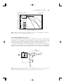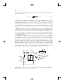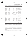
1
CHAPTER 18
Front Ends
Life is like a sewer. What you get out of it depends on what you put into it.
—Tom Lehrer†
18.1
INTRODUCTION
In Chapter 3, we dealt with optical detectors and their uses, from the output of the optical
system to the detector leads. Now it’s time to discuss the electronic front end—a ticklish
place, between the detector leads and the signal processing system. The front end’s job
is faithfully turning the detector output into a buffered, filtered electronic replica. Like
maintaining sewers, this is not glamorous work, but failure is very noticeable.
Bad front ends are too noisy, too slow, or both. The two are not unrelated; it’s easy
to make the front end fast if you are prepared to sacrifice signal-to-noise ratio, or if you
have lots of light. People tend to give up much too soon—it really is possible to do fast
measurements, at the shot noise limit, at low light intensities, with ordinary components.
This is most of what this chapter is about. It has some pretty heavily technical stuff in
it, so don’t worry too much if it doesn’t stick when you read through it; if you make the
same struggle for SNR yourself, it will become clearer very quickly.
A basic front end is just a transimpedance amplifier (current-to-voltage converter).
More advanced ones perform linear and nonlinear combinations of the signals from
more than one detector, as in differential measurements, and these operations must be
very accurate. Such advanced front ends allow you to make high stability measurements in
bright field, make simultaneous amplitude and phase measurements, or reject laser noise
with extremely high efficiency. A good one can spectacularly improve your measurement.
Throughout this chapter, we’ll be tossing around ultraquiet voltage and current sources,
and most of the time we’ll be behaving as though light source noise doesn’t exist. Don’t
be concerned about where we’re getting these magic parts—quiet voltages and currents
are constructed in Section 14.6.5 and Example 14.1, and source intensity noise is largely
vanquished in Section 10.8.6.
† Preamble
to “We Will All Go Together When We Go,” in An Evening Wasted with Tom Lehrer , private label
recording 1959, reissued by Reprise Records, 1966.
Building Electro-Optical Systems, Making It All Work, Second Edition, By Philip C. D. Hobbs
Copyright © 2009 John Wiley & Sons, Inc.
688
18.1 INTRODUCTION
TABLE 18.1.
Source
Major Sources of Noise in Front Ends
Type
Photocurrent
Load resistor
Amplifier
Amplifier
Shot noise
Johnson noise
Input current noise
Input voltage noise
Power supply
Ripple, regulator noise
18.1.1
689
Formula
iNshot = (2eId )1/2
iNth = (4kT /R)1/2
iN as specified
vN as specified
Dominates When
Bright light, large RL
Dim light, small R
Ideally never
Dim light, large RC , or a fast,
noisy amp
Only by blunders
Noise Sources
Since good front end design is largely a matter of balancing noise sources, it would be
worth beginning by reviewing the discussion of noise sources and calculations in Section
13.6.2. Table 18.1 summarizes the major sources of electronic noise encountered in front
end design.
18.1.2
Sanity Checking
Since the first edition of this book was published, the author has been receiving a certain
number of e-mails from people with detection problems, which are welcome. One common feature that has emerged is that specifications for optical instruments are often set
by people who are, ahem, not expert in optical measurements.† One of the most common
is to insist on wide bandwidth with high SNR at low light levels, for example, 50 MHz
at 20 pA of photocurrent, which cannot be done for reasons having nothing to do with
circuit design. Accordingly, here are a few representative rules of thumb for frequently
asked questions:
1. If you have N photons/s, your SNR will drop to 0 dB at a bandwidth B = N/2 Hz.
This is an inescapable limit based on counting statistics. Your maximum achievable
SNR is N /(2B), so since 20 pA is 1.24 × 10⁸ electrons/s, counting statistics limit
the SNR to 1.24 (0.9 dB) in 50 MHz.‡
2. Using a few high precision parts doesn’t get you a precise measurement. You can
measure a photocurrent very accurately, but accurate measurements of light intensity are very hard, and 24 bit A/D converters don’t help. It isn’t that photodiodes
aren’t good transducers—there are none better—but that the problem isn’t well
posed. The mapping of what you actually care about onto the photocurrent is just
about always imprecise at the level of a percent or two, due, for example, to etalon
fringes, calibration drift, background light, glints, and so on. There are honorable
exceptions, but not that many, and no measurement whatsoever can give a clear
answer to a fuzzy question.
3. Physicists (such as the author) are often prone to oversimplifying circuit requirements. It is not enough to aim at being “shot noise limited” or “Rf limited” and
† I’d
have been less complimentary, but then you couldn’t show them this section when the problem comes up.
Miller and Friedman’s book, Photonics Rules of Thumb, was written partly to help cure this problem.
‡ Time– bandwidth product issues like this show up in digital signal processing too—see Section 17.5.
690
FRONT ENDS
stop there. Filters do not cut off everything outside their passbands. Not everything has a one-pole rolloff. Shot noise limited SNR can be improved by getting
more photocurrent. There’s no substitute for calculating the SNR and frequency
response.
18.2
PHOTODIODE FRONT ENDS
This section is really an extended example of how to design a front end amplifier
for a visible or near IR photodiode, and how to get a factor of 4000 improvement
in bandwidth over the naive approach without sacrificing SNR. All the signal-to-noise
comparisons we’ll be making will be the DC signal power to the rms noise, which is
really a carrier-to-noise ratio (CNR) since what we think of as the signal will usually
be much smaller than the DC. The SNR is what we care about, so we’ll use that for
rhetorical purposes.
18.2.1
The Simplest Front End: A Resistor
Say we need with a detector subsystem whose 3 dB bandwidth is 1 MHz, a photocurrent
of 2 μA from a silicon photodiode whose capacitance is 600 pF at zero bias. Given a
detector whose output is a current, the easiest way to form a voltage from it is to shove
it into a resistor, say, 1 M, as shown in Figure 18.1. While this circuit generates an
output voltage Vo = Id R with admirable linearity (at least until we forward-bias the PD
too far), problems arise as soon as we ask about AC performance. Since the full signal
swing appears across the detector capacitance Cd , the output rolls off starting at
fRC =
1
,
2π RL Cd
(18.1)
which is 265 Hz at zero bias. This is a mere factor of 3800 slower than our 1 MHz design
point. As we saw in Section 3.4.5, most visible and NIR detectors can be operated at
reverse bias, which will reduce Cd (by as much as 7–10 times) while increasing the
leakage current slightly. This is nearly always an excellent trade, contrary to what you’ll
often read elsewhere. This diode’s data sheet says that its leakage current is about 0.5
nA at room temperature, for a 12 V reverse bias, and that this bias will reduce Cd by a
factor of 6, to 100 pF. That gets us to 1600 Hz, still not blazing fast. (We get to keep
Id
Id
D1
Cd
iNth
iNs
Cd
RL
Vbias
+
Figure 18.1. The world’s simplest front end: a load resistor.
RL
18.2
691
PHOTODIODE FRONT ENDS
that factor of 6 all through the design, however, so eventually it’ll take us from 170 kHz
to 1 MHz, which is a bit more impressive sounding.) Since the noise of the bias current
will be more than 30 dB below the photocurrent shot noise, this seems like a good thing
to do: we get a factor of 6 in bandwidth for a shot noise increase of 0.004 dB—which
is too small even to measure. (See Section 3.5.2.)
The signal voltage Vo goes as
Vo (f ) =
id (f )RL
,
1 + j 2π RL Cd f
(18.2)
as shown in Figure 18.2.
Somewhat surprisingly, though, the signal-to-noise ratio does not deteriorate at all.
The resistor’s iN and the shot noise current are both treated exactly as the signal is.
The reason for this is apparent from Figure 18.1: the signal and noise sources are all
connected in parallel.† Thus they all roll off together with increasing frequency, which
makes their ratios frequency independent, as Figure 18.2 shows. Any deterioration of
the signal-to-noise ratio of the measurement is due to the subsequent amplifier stages.
It’s not the poor amplifier’s fault, though—a source whose impedance changes by a
factor of 600 over the band of interest is not the best of neighbors.
As is usual when it’s circuit constants and not laws of nature which are in the way,
with a bit of ingenuity we can find circuit hacks to get around the rolloff without messing
up the SNR too badly.
Load Impedance (ohms)
1 Hz CNR (dB)
140
1E+06
5E+05
130
2E+05
120
1E+05
110
5E+04
100
2E+04
90
1E+04
80
5E+03
70
2E+03
1E+03
1E+02
1E+03
1E+04
1E+05
1E+06
1E+07
60
1E+08
Frequency (Hz)
Figure 18.2. Frequency response and narrowband CNR of the photodiode/load resistor combination of Figure 18.1, with RL = 1 M and Cd = 100 pF.
† Why
is it OK to move the bottom of Cd and id to ground?
692
FRONT ENDS
TABLE 18.2. Noise Degradation Due to the Johnson Noise of a 300 K Resistor
Id R(V)
5.1
1.3
0.57
0.32
0.20
18.2.2
iNth /iNshot
SNR
Id R(V)
0.1
0.2
0.3
0.4
0.5
−0.04
−0.17
−0.4
−0.6
−1.0
0.14
0.10
0.080
0.063
0.051
iNth /iNshot
SNR (dB)
0.6
0.7
0.8
0.9
1.0
−1.3
−1.7
−2.1
−2.6
−3.0
Reducing the Load Resistance
After reverse biasing, the first thing everyone thinks of is reducing the load resistance, because that reduces the RC product and speeds things up. This does reduce
the signal-to-noise ratio, because unlike the previous case, the resistor’s noise current
goes up as its value is reduced. There is nothing much lost by reducing the resistance
while shot noise still dominates—when the shot noise current is larger than the Johnson
noise current. The shot noise ceases to dominate when the two become equal, that is,
when the DC voltage drop across RL is 2kT /e (51 mV at room temperature), and we
enter the Johnson noise limit. Good instrument designers grind their teeth if they’re stuck
in the Johnson noise regime, since the data from an expensive optical system are being
seriously damaged by circuit limitations. In particular, running a photodiode into a room
temperature 50 load is always a mistake unless the light level is very high (milliwatts
in the visible). There are lots of things you can do to get decent bandwidth, so resist the
50 temptation. (As we’ll see later, it’s also possible to achieve an effective temperature
of the load resistance as low as 35 K at room temperature, so all is not lost.)
Remember too that the SNR versus thermal noise curve doesn’t have a sharp corner.
Table 18.2 shows the SNR degradation due to load resistor Johnson noise as a function
of the DC voltage across RL , which is a convenient way to remember it. If Id R = 0.2
V, then iNth = 0.5iNshot (6 dB down), and we’ve already lost 1 dB in SNR.
Making RL too big wastes both bandwidth and dynamic range, so it is usually best to
choose a value that drops 100 mV to 1 V. (Later we’ll do this with transimpedance amps
too.) For the present circuit, we will assume that a 1 dB loss is acceptable, so we’ll shoot
for a voltage drop of 0.2 V. With our 2 μA photocurrent, we’ll need a 100 k resistor,
which will improve the RC bandwidth to 16 kHz, a mere factor of 60 away from our
goal.
18.3
KEY IDEA: REDUCE THE SWING ACROSS Cd
Once we have carefully chosen RL and reverse-biased the photodiode, the circuit will
probably still be too slow, as we’ve seen. It’s time to change the circuit topology and
see if that works well enough. We may observe that the source of the poor bandwidth
of the load resistor approach is that the full signal swing appears across Cd . If we
make both ends of the photodiode work at constant voltage, then there will be no swing
across Cd , and hence no capacitive current (see Section 15.3). Making the swing small
requires making the load impedance small. How can we do that without degrading the
noise?
18.4 TRANSIMPEDANCE AMPLIFIERS
18.4
693
TRANSIMPEDANCE AMPLIFIERS
One way to do it is to make the detector work into a virtual ground, as shown in
Figure 18.3. Although the inverting input of A1 draws no current, feedback forces the
voltage there to be close to zero at all times. The way this works is that A1 senses the
voltage across Cd and wiggles the other end of Rf to zero it out. Provided A1 has high
open-loop gain AVOL , the swing across Cd is greatly reduced, and the bandwidth greatly
improved. The amplifier input adds a significant amount (2–20 pF) of its own capacitance
Cin , which must be added to Cd . Because this circuit is so important in applications, it’s
worth spending a little time analyzing its bandwidth and noise.
The voltage gain of A1 is not infinite, so that the swing is not exactly zero; to produce
an output voltage Vo , A1 requires an input voltage Vi = Vo /AVOL . AVOL rolls off at
high frequency, which limits the bandwidth improvement. Prepackaged op amps have
their open-loop frequency responses carefully tailored to make them easy to use, which
in practice means that they roll off like 1/f (6 dB per octave), with a nearly constant
90◦ phase shift from a low frequency all the way to their unity gain crossover at fT .
The uppermost curve of Figure 18.4 shows the response of an LF356 (105 dB DC gain,
4 MHz fT ), which is of this character. The advantage of this is that any closed-loop
gain will result in a stable and well-behaved circuit that settles quickly. This approach
is called dominant pole compensation; its drawback is wasted bandwidth at high
closed-loop gain, which does not greatly concern us here. Mathematically, AVOL is
approximately
ADC
.
(18.3)
AVOL (f ) =
(1 + jf/fdom ) (1 + jf/f2 )
The exact values of the DC gain ADC and the dominant pole frequency fdom are
not well controlled from unit to unit. Their product, known as the gain–bandwidth
product (GBW), is approximately equal to the unity gain crossover frequency fT and
is a well-controlled parameter. The other term in the denominator, which is a pole at
frequency f2 , represents the effects of limited bandwidth in other stages of the amplifier.
In amplifiers intended for use at unity gain, f2 is always higher than fT , but not by
much—a factor of 1.2 to 4, thus contributing an additional phase shift at fT from 40◦
down to 15◦ .
Cf
Rf
Id
D1
−
Cd
+
Output
A1
−Vbias
Figure 18.3. Op amp transimpedance amplifier.
694
FRONT ENDS
Gain (V/V)
1E+05
Phase (deg)
−180
f0
1E+04
−135
1E+03
AVol
1E+02
−90
φL
AVL
1E+01
−45
1E+00
Hfb
1E−01
0
1E−02
1E+02
1E+03
1E+04
1E+05
1E+06
1E+07
1E+08
Frequency (Hz)
Figure 18.4. Frequency responses of parts of the transimpedance amplifier loop. A1 is an LF356
op amp, Rf = 100 k, Cf = 6.3 pF, Cd = 100 pF. See Section 18.4.1 for the choice of Cf .
When we close the feedback loop by connecting some network between the output
and input of the amplifier, we can predict the frequency response of the resulting circuit
from the open-loop responses of the amplifier and the feedback network.
The feedback network here is the series combination of Rf and Cd , whose voltage
gain is
1
.
(18.4)
Hfb (f ) =
1 + j 2πf Rf Cd
Roughly speaking, the closed-loop gain of an amplifier starts to roll off at about the point
where the product of the open-loop gains of the amplifier and feedback network falls to
0 dB. Extra phase shifts due to the other poles in the circuit can modify this somewhat,
as we’ll see below, but it’s within a factor of 2.
Far down on their slopes, the responses of the feedback network and the amplifier
are approximately −jfRC /f and −jfT /f , respectively. Their product is approximately
−fRC fT /f 2 , and the loop bandwidth of the resulting transimpedance amplifier is therefore approximately
(18.5)
fCL ≈ fRC fT ,
which for the LF356/100 k/100 pF combination is (16 kHz · 4 MHz)1/2 , or about 250
kHz. The transimpedance rolls off somewhat earlier than this, since it depends on the
magnitude of the impedances of the feedback elements, and not merely on their ratio.
Calculating the transimpedance bandwidth is a straightforward exercise—you put a current into the summing junction and calculate how much goes through Rf and how
√ much
through Cd . Without going hip deep into algebra, you lose a factor of between 2 and
2 in bandwidth, depending on the details of the frequency compensation scheme, so for
a rule of thumb we’ll say that
√
fRC fT
.
(18.6)
f−3 dB ≈
2
18.4 TRANSIMPEDANCE AMPLIFIERS
695
We’ll actually get around 130 kHz transimpedance bandwidth from the LF356 circuit, a
factor of more than 8 improvement.
This is still fairly far from 1 MHz, but getting a lot closer. We need about 8 times
more bandwidth, so if we choose an amp with a bandwidth 60 or so times higher (i.e.,
250 MHz), then we ought to get there. Right? Well, sort of. There are two things we’ve
left out of this picture. One is noise, and the other is frequency compensation. Frequency
compensation is easier, so let’s knock that off first.
18.4.1
Frequency Compensation
The equation for the closed-loop noninverting gain of a feedback amplifier is
AVCL (f ) =
AVOL (f )
,
1 + AVOL (f )Hfb (f )
(18.7)
where Hfb is the gain of the feedback network (usually a voltage divider). For frequencies where the loop gain AVL = Hfb AVOL 1, this simplifies to 1/Hfb . Looking at
the denominator, clearly what happens when AVL ≈ 1 will have a great effect on the
closed-loop behavior. If the loop gain has a phase of −180◦ when it crosses unity magnitude, the denominator will go to zero and the closed-loop gain will be infinite, which
means that the circuit will oscillate fiercely near there (this is a sufficient but not necessary condition for oscillation). On the other hand, if the phase is −90◦ , then there will
be a well-behaved RC -type corner there. The difference between the actual open-loop
phase and −180◦ is called the phase margin. In practice, as long as the worst-case phase
margin is greater than 45◦ or so, the closed-loop response will not exhibit undesirable
peaking, and the time-domain step response will not overshoot too much.
From (18.7), we can show that an amplifier whose phase margin is 90◦ , that is, a
single RC rolloff, has a closed-loop 3 dB corner frequency fc at exactly the open-loop
unity gain crossover, whereas one with 45◦ margin has its corner at an open-loop gain
of only 0.52.
In order to achieve a 45◦ phase margin, we need to stop the rolloff of the feedback
network at a frequency about equal to the closed-loop corner. We can do this by putting
a capacitor Cf across Rf , where
Cf =
1
√
,
2π Rf fT fRC
(18.8)
which gives a phase margin of between 45◦ and 60◦ , depending on how fast the amplifier
is. An alternative is to put a small resistor Rs in series with the photodiode, where Rs is
Rs =
1
√
2π Cd fT fRC
.
(18.9)
In complex-variables language, these additions put a zero into the transfer function
(see Section 15.4.3). The exact value of Rs or Cf that gives the optimal trade-off of
peaking versus bandwidth for your application depends on what you are most interested
in, so take these values as starting points. Beware of device-to-device variations in Cd
and GBW if you’re making more than one or two copies. If you crank Cf down to the
696
FRONT ENDS
absolute lowest tolerable value in your lab prototype, Murphy’s law dictates that the next
100 photodiodes will be at the upper spec limit for capacitance, and all 100 circuits will
oscillate merrily. It is axiomatic that all prototypes contain at least one perfect component,
which works beautifully but is totally unrepresentative of normal production units.
Although the approximation (18.6) (f−3 dB ≈ fCL /2) is good enough for early design
purposes, it is worthwhile to carefully plot the frequency response of the transimpedance,
because it hasn’t the same shape as the closed-loop gain. With the approximate expression
(18.3) for the op amp’s gain, the transimpedance is given by
Zm =
AVOL Zf
,
1 + AVOL + j 2πf Cd Zf
(18.10)
where Zf is the complex impedance of the parallel combination of Rf and Cf .
Figure 18.5 shows the performance of the transimpedance amplifier, with frequency
compensation by Cf = 6.3 pF, as calculated from (18.8). The transimpedance bandwidth
is only about half f0 , and it rolls off very steeply (approximately 18 dB/octave, equivalent
to 3 poles). Also shown are the open-loop gain and the closed-loop noninverting gain,
which we will encounter in the next section.
18.4.2
Noise in the Transimpedance Amp
Confusion reigns supreme in discussions of noise in transimpedance amps. Let’s try
to boil it down to something reasonably memorable. Figure 18.6 shows a simple but
adequate noise model of a transimpedance amp plus a photodiode. It is visually obvious
that all the current sources are treated identically: Id , iNshot , iNth , and INamp appear in
parallel. The Johnson noise iNth of Rf really appears across Rf , of course, but because
the impedance of the op amp output is very low, the other end of the noise current
source is at ground for noise purposes. The signal current thus appears in parallel with
the current noise sources, just as in the simple load resistor case, so the rolloff in the
frequency response will once again not degrade the signal to current noise ratio.
Gain (V/V)
1E+05
f−3dB
1E+04
Transimpedance (ohms)
100,000
50,000
f0
30,000
1E+03
20,000
Zm
1E+02
10,000
AVL
1E+01
5,000
1E+00
1E-01
1E-02
1E+02
3,000
AVCL
1E+03
1E+04
2,000
1E+05
1E+06
1E+07
1,000
1E+08
Frequency (Hz)
Figure 18.5. Performance of the transimpedance amplifier.
18.4 TRANSIMPEDANCE AMPLIFIERS
697
Cf
Rf
i Nth i Ns i Namp
−
Cd
+
Output
A1
eNamp
Figure 18.6. Simplified noise model of the transimpedance amplifier. All noise sources except
eNamp are treated exactly as the photocurrent and shot noise, so that only eNamp changes the SNR.
The only noise source that is treated differently is the amplifier’s voltage noise, eNamp .
Because the amplifier amplifies only differential signals (i.e., those in which its inputs
move in opposite directions), the model noise source can be put in either input lead.
Here we put it in the noninverting lead, which simplifies the analysis: clearly, eNamp will
be multiplied by the noninverting gain of the amplifier, AVCL —which is therefore the
noise gain of the stage. (See Section 13.1.) Taking Zf as the complex impedance of the
feedback element (Rf in parallel with Cf ),
AVCL =
AVOL
.
AVOL
1+
1 + j ωCd Zf
(18.11)
For frequencies well within the loop bandwidth, the resulting equivalent noise current is
approximately
(18.12)
iN ≈ (2πf CD )eNamp .
This gain begins to rise at the RC corner frequency of Cd and Rf , just where the
signal rolloff would have begun if we were using a simple load resistor approach; in fact,
the SNR as a function of frequency is identical to that of the same amplifier connected
as a buffer following a photodiode and load resistor, which is reassuringly reasonable.
All we’ve done is to tailor the frequency response by using feedback to jiggle the far
end of Rf ; this shouldn’t get us something for nothing. The addition of Cf or Rs
doesn’t fundamentally change this, but it causes the input referred noise to level off at
the frequency of the feedback zero.
If the op amp’s voltage noise is very low, or if we are not trying to get a huge
bandwidth improvement through the (fT · fRC )1/2 mechanism, this rising noise contribution will not limit us. If we are relying heavily on this mechanism, though, the
noise may increase catastrophically: it will begin to dominate all other noise sources at
approximately f3 , where
f3 =
1
2π eNamp Cd
2
2eId + iNamp
+
4kT
.
Rf
(18.13)
698
FRONT ENDS
We can see this nefarious gotcha in action in Figure 18.7, which is a plot of the
noise power spectral density of our LF356 circuit. The voltage noise is unimportant at
low frequency but rises to dominate the entire noise budget. The log–log plot is a bit
deceiving; plotting the noise power versus frequency on linear scales, as in Figure 18.7,
gives a more visceral feel for the problem. It only gets worse when we try to go faster.
One reason for the confusion is that most of us have a persistent idea that noise spectra
are flat or nearly so—which is often true, but not here.
1 Hz Noise
1 Hz CNR (dB)
1E-06
130
f−3dB
CNR
5E-07
125
3E-07
2E-07
Total Noise
1E-07
120
5E-08
115
Dark Noise
3E-08
2E-08
1E-08
1E+03 2E+03
110
5E+03 1E+04 2E+04 5E+04 1E+05 2E+05 5E+05 1E+06
Frequency (Hz)
1 Hz Noise (V)
1 Hz CNR
3E-07
f−3dB
2.5E-07
2.106
CNR
2E-07
1.5E-07
Total Noise
1.106
1E-07
5E-08
Dark Noise
0E+00
0E+00
5E+04
1E+05
1.5E+05
2E+05
0
2.5E+05
Frequency (Hz)
Figure 18.7. Noise performance of the transimpedance amplifier of Figure 18.3, showing the
dominance of dark noise (i.e., additive circuit noise) at high frequency. At right, the same data
plotted on linear scales. This shows the true character of the eNamp problem.
18.4 TRANSIMPEDANCE AMPLIFIERS
18.4.3
699
Choosing the Right Op Amp
In order that the op amp not dominate the noise, choose it by the following rules
(worst-case specifications apply):
1. iNamp < 0.5iNth . We’ve chosen Rf so as to lose no more than 1 dB to Johnson
noise, so don’t mess it up by choosing an amp whose current noise is as big or
bigger than Rf ’s.
2. eNamp < 0.5eNth . Similarly, we don’t want the amplifier’s voltage noise to dominate
under any circumstances.
3. eNamp < 0.5iNth /(2πf−3dB (Cd + Cin ) ). This ensures that the rising noise current
due to eNamp doesn’t begin to dominate anywhere in the band we care about. (Cin
is included explicitly here as a memory jogger—it always has to be added in.)
2
/fRC . The amplifier has to be fast enough to raise the bandwidth
4. fT > 2f−3dB
sufficiently.
2
5. fT < 10f−3dB
/fRC . Going too fast is asking for trouble. The size of the noise peak
will be so large that extensive filtering will be needed to get rid of it, and the
circuit may even oscillate.
6. If finding an amp that satisfies Rules 1–4 runs into money, either spend it, or use
a circuit hack to get round it. Don’t economize here.
7. It is not always necessary to use a unity-gain stable amplifier because of the Cd Rf
gain peak, but watch the frequency compensation extra carefully if you don’t.
Using a decent part, which has guaranteed specifications for noise and gain bandwidth,
usually pays for itself many times over by the relaxation this permits in the specs of the
optical system. Use worst-case design here, and leave a safety margin, especially on
eNamp . The log–log plots are deceiving; if eNamp dominates only near the high end, that
is as bad as dominating over the whole band, because there’s a lot more high end than
there is low end.
Table 18.3 lists some good op amps for use in photodiode front ends. The exact
circumstances in which each is superior are somewhat complicated: try the low voltage
noise ones with bright light, and the low current noise ones at low light. Remember
that op amp input capacitance has the same effect as photodiode capacitance, so that the
musclebound FET units with the high Cin are not as universally useful as their low noise
specs would suggest. This remains true even if we put them on steroids, as the following
example shows.
Example 18.1: External JFET Differential Pair. It’s often possible to improve the
noise performance of op amp TIAs by adding a discrete JFET front end. By adding a
pair of 2SK369s with a voltage gain of 20 or so, running at ID = 10 mA (VGS = −0.1
V), we get 1 Hz vN = 0.7 nV, which is 1.0 nV for the pair combined. Keeping VDS
down to 6 V or so keeps the gate current below 5 pA, so iN should be in the femtoamps.
Most of the input current noise comes in via the drain-gate capacitance, so we’ll assume
a cascode stage. Getting a stage gain of 20 requires RL = 20/gm = 400 .
The resulting amplifier has about 90 pF of inverting input capacitance, unfortunately,
due to the very large die size of the JFETs. With the BJT cascode, the 50 pF feedback
700
FRONT ENDS
TABLE 18.3. Suggested Op Amps for Front Endsa
Device
ManufT
vN @10 kHz iN @10 kHz Cin Cin · vn
facturer (MHz) (nV/Hz1/2 ) (pA/Hz1/2 ) (pF) (typ)
FET
LF356
OPA627
NS
TI
4
20
12t
6
0.01t
0.0025
3t
7t
36
32
OPA129
TI
1t
15t
0.0001
1.5t
22
AD795
OPA657
AD
TI
1.6t
1600
11
4.8t
0.0007t
0.0013t
2t
2.6t
18
12
OPA656
TI
230
7t
0.0013t
1.7t
12
Bipolar
OP-27
OP-37
OPA687
AD
AD
TI
8
45
3800
3.8
3.8
1.1
0.6
0.6
3.3
2t
2t
1.8t
7
7
2
LT1028
LT
50
1.1
1.6
5t
4.8t
AD829
AD8397
LM6311
LM7332
LMH6624
LME49710
AD
AD
NS
NS
NS
NS
600t
69t
80t
21t
1500t
55t
2
4.5t
2.3t
15.5t
0.9t
4.7
1.5
1.5t
3.5t
1t
2.3t
1.6t
3.2t
1.4t
2.5t
5.5
6.3
8.8t
2.2t
3t
2t
7.5
OP-470
AD8397
ADA4898-1
MC33078
AD
AD
AD
ST
6t
33t
33t
10
5
4.5t
0.9t
4.5t
0.4t
1.5t
2.4t
0.5
2t
1.4t
1.5t
12t
12
6.3
1.4
54
Remarks
Cheap, good
OPA637 decomp
version
Good in low light,
expensive
Good at low Id
±5 V, AV > 10 but
fast and quiet
Unity-gain
compensated 657
Good for Id > 5 μA
AV > 5
AV > 40, 35 μA Ib , 5
V
Good for low Rp
diodes (e.g., InAs)
3600 V/μs slewing
Poor data sheet
Drives unlimited CL
±6V, poor datasheet
LM4562 dual,
LME49740 quad
Quad; OP270 dual
±12V
±12V—amazing part
Dual, largish Cin
±15 V devices due to their much greater dynamic range. Unless noted, devices can use ±15 V
supplies and are unity gain stable.
a Mostly
capacitance times the noise at its emitter contributes a 1 Hz current noise
iNC (f ) = 2πf Cdg kT
2
,
eID
(18.14)
which is 0.05 pA at 1 MHz, rising 20 dB/decade. With a total summing-junction capacitance of 190 pF including Cd , Rule 3 shows that even a nice FET like this one is 16
dB too noisy for our application. (A pair of BF862s would be a little closer, but still at
least 12 dB too noisy.) The biggest benefit of this approach is the very low Cin you can
get by cascoding, which allows the use of much bigger feedback resistors, as we’ll see
below.
18.4 TRANSIMPEDANCE AMPLIFIERS
18.4.4
701
No Such Amp Exists: Cascode Transimpedance Amplifiers
In our design, if we are aiming at getting to 1 MHz transimpedance bandwidth, Rules
1–5 lead to an amplifier with the following characteristics: INamp < 0.20 pA/Hz1/2 ;
eNamp < 0.32 nV/Hz1/2 ; 250MHz < fT < 1250 MHz. No such amplifier exists, not even
with an external input stage. Now what? Another circuit hack, of course.
Recall that our reason for using the transimpedance amplifier was to get rid of the
voltage swing across Cd . We can do this another way, by using a common-base transistor
amplifier, as shown in Figure 18.8 (Resistor RE will come in later—ignore it for now.)
The transistor faithfully transmits its emitter current to its collector, while keeping its
emitter at a roughly constant voltage. This idea is used in common-emitter transistor
amplifier design to eliminate severe bandwidth limitations due to collector–base feedback capacitance (the Miller effect). The resulting amplifier configuration resembles a
two-layer cake and is called a cascode. The cascode idea works here as well. In the
Ebers–Moll transistor model, the small signal resistance rE of the transistor’s emitter
circuit is
kT
,
(18.15)
rE =
eIC
where kT /e is 25 mV at room temperature (rE is intrinsic to the transistor and should not
be confused with the real metal film resistor RE ). Thus our 2 μA photocurrent sees a
resistance of 12.5 k, so that the RC bandwidth increases by a factor of 8 immediately,
to about 130 kHz. What is more, the collector circuit has a shunt capacitance set only by
the output capacitance Cob of the transistor and Cin of the op amp, which can be chosen
to be much less than Cd , so that we can raise Rf if we choose without losing bandwidth
or suffering from serious eNamp multiplication.
Aside: rE Auto-scaling. An interesting feature of the nonlinearity of rE is that it
automatically adjusts to an increase in photocurrent by reducing the RC product. In
Section 18.2.2, we chose a value of Rf proportional to 1/Id ; that’s just what Q1 does,
while maintaining the 8× bandwidth improvement.
On the other hand, we can no longer improve the bandwidth by simply using a faster
amplifier, and besides, the bandwidth of the circuit depends on Id . Sure, the limitations of
the transimpedance stage are less of a worry, but if we can’t get the (fRC fT )1/2 bandwidth
improvement, have we really gained anything? The answer is yes. First, remember that
the RC rolloff moves 8 times higher in frequency, which by itself often makes the
bandwidth adequate. Second, we are not powerless to improve the bandwidth further: in
Rf
Id
Q1
D1
-
Output
A1
+
Cd
RE
−Vbias
Figure 18.8. Using a common-base amplifier greatly reduces the effects of Cd and significantly
improves the SNR as well. External biasing via RE provides even more improvement.
702
FRONT ENDS
fact, there are two ways to fix these minor warts while gaining even more bandwidth.
First of all, though, let’s look at the SNR of the cascode to see what this bandwidth
improvement costs us.
18.4.5 Noise in the Cascode
In the simple load resistor case, the signal, shot noise, and Johnson noise contributions
rolled off together, resulting in a constant SNR. Here we’re not quite that lucky, because
there is an additional noise contribution from Q1 , which rises with frequency; it is much
more benign than the eNamp problem with transimpedance amplifiers, however.
Any transistor has some noise of its own. A simple noise model of a BJT is shown
in Figure 18.9, which neglects only the Johnson noise of the base resistance rB (normally only a problem when IC 1 mA). The active device in the model has infinite
transconductance (i.e., emitter impedance of 0 ) and no noise.
Noise current inB is the shot noise of the base current IB = IC /β, which is inescapable,
while iNC is the shot noise of the collector current, which shows up in parallel with the
small signal emitter resistance rE (we ignore the difference between IC and IE for now,
and just talk about the collector current IC ). If the emitter is grounded, all of iNbias goes
from ground into the emitter, and so contributes full shot noise to the collector current.
On the other hand, if the emitter is biased by a current source (e.g., a resistor many times
bigger than rE ), all the noise current has to go through rE , and none at all winds up
in the collector current (the real emitter lead does jiggle up and down slightly, though).
It may be more comforting to talk about the Thévenin model, where the shot noise is
converted to an emitter-base voltage by dividing by the transconductance, so that the
voltage noise is
√
2eIC
2
= kT
,
(18.16)
eNshot =
gm
eIC
to which must be added the Johnson noise of the extrinsic base resistance RB , usually
40–100 . (They are added in RMS, of course.† )
iC
i
nb
r
E
i
Nbias
Figure 18.9. Simplified noise model of a bipolar junction transistor (BJT).
† Don’t
try to calculate this noise contribution by applying the Johnson noise formula to rE —it’s 3 dB lower
than that, and the physics is completely different.
18.4 TRANSIMPEDANCE AMPLIFIERS
703
Whichever way you prefer, if the photodiode impedance is infinite, the transistor does
not contribute noise to the collector current. Referring back to Figure 18.8, we see that
our diode really has capacitance, so the finite impedance of Cd makes iNC split between
Cd and rE by the ratio of their admittances (remember we’re dealing with RMS averages
of noise here, so only the magnitude matters).
A couple of lines of algebra then give the Q1 contribution to the noise:
ωCd
≈
iNQ1 = VNQ1 1 + (ωCd rE )2
2eIC rE2 ωCd
1 + (ωCd rE )2
(18.17)
(you can instantly see this if you use the Thévenin equivalent circuit for iNC and rE ). In
an unbiased cascode, where IC is all from photocurrent, this contribution exactly cancels
the rolloff of the photocurrent shot noise, so that the collector current of Q1 has full shot
noise at all frequencies. Thus the 1 Hz SNR rolls off exactly as the signal does and is 3
dB down at the signal corner frequency fc . This is at least easy to remember.
On the other hand, if the applied emitter current IEq has only δ times full shot noise
power, as it will in a minute, the iNC contribution will start to dominate the bias current
noise at a somewhat lower frequency
√
fSNR = fc δ,
(18.18)
which turns out to be a serious limitation.
Aside: Q1 Voltage Noise. If the RB noise of the transistor is important, its voltage
noise has to be added in to the numerator surd of (18.17), which becomes
iNQ1
= 2eIC rE2 + 4kT RB ωCd
1 + (ωCd rE )2
.
(18.19)
(BJT noise models have a good handle on the fundamental physics, so BJT circuits
actually follow the model.)
18.4.6 Externally Biased Cascode
Of the two promised ways we can improve the bandwidth, the simpler one is to apply a
very quiet DC bias current IEq to the emitter of Q1 , in addition to Id . The value of rE
can be reduced considerably this way, further improving fRC . For example, if we use
IEq = 20 μA, rE drops to 1.25 k and fRC is 1.27 MHz—quite a bit better than our
original 1600 Hz, and enough for the circuit requirement. We start running into the input
capacitance Cin of the op amp, which limits how fast we can go just the way Cd did
before. Switching to a slightly faster op amp such as an LF357 and using Cf = 0.5 pF
overcomes Cin and gets us to a 1.1 MHz 3 dB bandwidth for the whole circuit. The net
bias current now has 10 times less than full shot noise, so (18.18) predicts that the SNR
will be down 3 dB at only 330 kHz, which is not good enough. We could just as easily
use IEq = 200 μA, so that the shot noise corner will be at 1.3 MHz, but this starts to get
us into trouble. Let’s look at why.
704
FRONT ENDS
18.4.7 Noise Considerations
Generating that very quiet (much less than full shot noise) current is easy: a metal film
resistor RE to a well filtered supply is all that is required, provided that the resistor drops
a large enough voltage.
If we make RE drop N times kT /e, the noise power due to iNbias will be reduced by a
factor of N 2 . In our example, with IEq = 200 μA and Id = 2 μA, if RE IEq = 2.5 V, the
shot noise power from the bias current will be reduced to 10−2 times the photocurrent
shot noise power, a negligible addition.
The real limitations come from base current shot noise and Johnson noise in RE . √
The
base current IB has full shot noise, which limits the bias current noise to at least 1/ β0
times full shot noise current. (That β0 is the DC current gain, which is what’s relevant
even at high frequency, since it’s the DC value of IB that sets the shot noise level.) Start
out with a BFG25A/X or BFT25A, but consider using a superbeta transistor (β ≈ 1000)
like an MPSA18. Darlingtons can have huge betas, but they’re fairly noisy, and so they
often make disappointing bootstraps. From (18.16), the voltage noise of the driver stage
is high, and the transconductance of the output stage is also high, leading to lots of noise
current unless the driver stage is run at a pretty high current itself. A single superbeta
transistor, perhaps with its own collector bootstrapped, is usually a better choice when
base current shot noise is a limiting factor. Homemade Darlingtons can be better—you
can make a good one from two BFG25A/Xs. At low currents you can make the bootstrap
a fast JFET (e.g., a BF862). That gets rid of the base current problem, at the expense of
lower transconductance and higher voltage noise.
Resistor RE sources its full Johnson noise current into the summing junction, so that
the net Johnson noise is that of the parallel combination of Rf and RE . For convenience,
we could simply put a 75 k metal film resistor in parallel with D1 (assuming that
−Vbias = −15 V). The improvement is enough to meet our design bandwidth, but the
noise is degraded by 3 dB, and we have to raise the positive supply enough that the
voltage drop across Rf doesn’t saturate the op amp. This is a viable solution if we can
make −Vbias bigger, perhaps −45 V, so that RE can grow and its Johnson noise current
thereby shrink (as a by-product Cd will shrink, which is a great help). A simple charge
pump followed by a capacitance multiplier will get you a nice quiet −24 V, which is
usually lots.
The calculated transimpedance gain and CNR of the cascoded transimpedance amplifier appear in Figure 18.10, with and without an additional 30 μA IEq . Using a higher
bias current makes it worse rather than better; there’s a big improvement in bandwidth
and mid-frequency SNR, but even in this best case, the 1 MHz SNR is down by 6 dB
due to the bias current noise, so we have to go a bit further still.
Aside: DC Offset. A minor drawback to the externally biased cascode circuit is that
the DC level at the output of the transimpedance amplifier is no longer zero at zero
photocurrent. This offset can be trimmed out, but it will drift somewhat with temperature,
so that more circuit hackery is necessary if a highly stable DC level is needed. Most of the
time it isn’t, especially since other drift sources such as etalon fringes are normally much
more serious. If we can raise +Vbias enough, a resistor from there to the summing junction
can get rid of the DC offset without adding too much Johnson noise. A diode-connected
transistor in series with this resistor will provide first-order temperature compensation.
18.4 TRANSIMPEDANCE AMPLIFIERS
Transimpedance (Ohms)
705
1 Hz CNR (dB)
1E+06
5E+05
125
2E+05
1E+05
5E+04
120
Unbiased Zm
2E+04
Biased Zm
1E+04
Unbiased CNR
5E+03
Biased CNR
2E+03
Shot Noise CNR
1E+03
0.01 0.02
115
110
0.05 0.1
0.2
0.5
1
2
5
10
Frequency (MHz)
Figure 18.10. Calculated response and CNR of the cascode transimpedance amplifier of
Figure 18.8 at Id = 2 μA, with and without a 30 μA IEq .
18.4.8 Bootstrapping the Cascode
If even small DC shifts are obnoxious, or the required value of IEq is so large that base
current shot noise is a limitation, another technique is superior: bootstrapping. As shown
in Figure 18.11, driving the cold end of D1 with a follower Q2 forces the drop across
Cd to be constant, at least at frequencies where XC2 is small and XCd rE2 .
In order for this to be any use, the bootstrap has to have much lower impedance
than the cascode, so make IC2 IC1 . The bootstrap circuit is a bit more complicated to
analyze for noise, but the results are nearly the same as for a biased cascode with the
R
Id
f
Q1
D1
−
Output
A1
+
Cd
Q2
∞
−Vbias
Figure 18.11. Bootstrapping the unbiased cascode circuit reduces the effects of rE and has performance similar to that of the biased cascode, without the offset current due to RE .
706
FRONT ENDS
same collector current. Assuming IC2 IC1 , the noise current from Q2 flowing to the
emitter of Q1 via Cd is
iNbootstrap ≈
Id 2eId ωCd rE1
IC2
(18.20)
to leading order in ω. This is approximately (IC2 /Id )1/2 times smaller than in the unbiased
case. It grows linearly with ω, so although the bandwidth is increased by IC2 /Id , the
SNR is down 3 dB at about ω = (IC2 /Id )1/2 /(rE2 Cd ), just as in the biased cascode case.
Bootstrapping basically replaces the rE1 of cascode device Q1 with the rE2 of follower Q2 , which gives an improvement of IC2 /IC1 times in bandwidth. By essentially
eliminating the capacitive loading on Q1 , it also eliminates the effects of Q1 ’s voltage
noise.
This trick is reminiscent of the old joke about the cowboy who, after he fell into a well,
“pulled himself up by his bootstraps.” Bootstrapping suffers the same multiplication of
the voltage noise of the follower that we saw in the transimpedance amplifier. However,
here the RC product is not Rf Cd but rE1 Cd , a factor of 8 smaller, and the follower’s
vN is usually smaller as well, so this is not nearly as great a problem as it is with the
transimpedance amplifier.
We wouldn’t be doing this if current errors weren’t important, so we’ll use a superbeta
MPSA18 with IC2 = 290 μA. The largish Ceb of this device appears in parallel with Cd ,
so it hardly matters; the Ccb forms a voltage divider with Cd , but since it’s 50 times
smaller, it doesn’t matter much either. The 7 μA flowing through Rbias makes the cascode
a bit faster, and the offset voltage and drift are canceled by the matching resistor and the
VBE of Q3 . All this together improves the CNR to 1 dB above the shot noise limit in the
flatband, degrading to 3 dB above shot noise at 1 MHz, and gets us a 3 dB bandwidth
of 2 MHz. The final circuit is shown in Figure 18.12, its calculated performance in
Figure 18.13(a). Figure 18.13(b) shows the prototype’s measured performance, which is
somewhat better than the worst-case calculation. The measured shot noise/dark
+15V
2N3904
Cf
2M
0.25 pF
Rf
Q3
Id
Q2
BFG25A/X
Q1
MPSA18
D1
30k
301 k
−
+
Cd
Output
A1
LF357A
100 pF
Rbias
10 nF
20k
2M
−15V
Figure 18.12. The final circuit: cascode Q1 plus bootstrap Q2 cope with the obese 100 pF diode,
and diode-connected Q3 cancels the VBE drift of Q1 .
707
0.2
0.5
1
2
5
10
110
115
120
125
1 Hz CNR (dB)
(b)
Figure 18.13. Performance of the final circuit. (a) Calculated CNR is down only 3.3 dB at 1 MHz. (b) Output of the prototype: bottom—dark noise;
top—noise with 2 μA photocurrent, showing better than calculated SNR. The setup has an overall voltage gain of 2.7.
(a)
Frequency (MHz)
0.05 0.1
1 Hz CNR
Shot Noise
1 Hz CNR
5E+04
0.01 0.02
1E+05
2E+05
3E+05
Zm
Transimpedance (Ohms)
5E+05
708
FRONT ENDS
noise ratio is 9.5 dB at low frequency, dropping to 4.5 dB at 1 MHz.† These numbers
correspond to total noise 0.5 dB over shot noise at low frequency, rising to 1 dB over
shot noise at 1 MHz. There are no unpleasant surprises, which helps us to be confident
that we finally understand the circuit.
18.4.9 Circuit Considerations
Although the cascoding and bootstrapping tricks seem like a free lunch, nevertheless,
like all circuit hacks, they have their limitations. The linearity of the transistor’s gain
may not be as good as that of the photodiode. Normally a small amount of bias (20 μA
or so) will linearize the transistor well enough. For the most critical applications, use a
highly linear transistor, a Darlington, or (if driven to it) FET. FETs have no base current
nonlinearity, but their transconductance is low and their noise high, so they don’t usually
work as well. The BF862 is sometimes an exception.
18.4.10 One Small Problem . . . Obsolete Parts
Most inconveniently, National Semiconductor discontinued the 75-cent LF357 in 2004.
There’s no single replacement with its particular combination of virtues, not even among
the fancy $50 parts (See Table 18.4). For the current design, we need Rf ≥ 300 k to
keep the SNR drop to 0.5 dB at low frequency and 1 dB at 1 MHz with a minimum Id of
2 μA. If the maximum Id is less than 100 μA, we can get away with a ±5 V amplifier,
in which case things are easier: we can drop in a $5 OPA656, and we’re done—its input
capacitance is about the same as the 357’s and it has lower voltage noise. We can leave
Cf the same, since the 656 is unity gain stable and we don’t need all of its bandwidth.
Performance will be nearly identical to the LF357 circuit.
If the photocurrent can go much higher than that (e.g. 500 μA), we really need the
extra 10 dB dynamic range we get from ±15 V supplies. In that case we can either
use a compound amplifier, for example, that BF862 differential pair we looked at earlier
running into a ±15 V op amp, or an external fixed-gain buffer inside the feedback loop.
The external JFET pair is more easily frequency compensated (e.g., with a lead–lag
network around the op amp), but the fixed-gain booster doesn’t mess up the nice input
accuracy of the OPA656.
Alternatively, we can give up about 1 dB of SNR and use the ±15 V OPA627. Its
other specs are excellent for the purpose, but its input capacitance is 8 pF, so it will
oscillate with a 300 kRf , and when we increase Cf to compensate, it becomes too
slow. Thus we have to use Rf ≈ 80 k, which costs us 0.7 dB in SNR at all frequencies.
A bipolar op amp such as an OP37 will have lower eN and Cin , but its 1 Hz iN is 0.6 pA,
which is comparable to the 0.8 pA shot noise and so costs us 2 dB SNR in the present
instance, though it’ll be superior at higher Id . Note that these problems have nothing
to do with photodiode capacitance, which has already been fixed by the bootstrapped
cascode—the problem here is amplifier Cin , that is, the op amp tripping over its own
big feet. In general, technological change has made TIA design easier in some ways and
harder in others.
† Remember
that the distance between the two curves is total noise/Johnson noise, not shot noise/Johnson noise.
18.4 TRANSIMPEDANCE AMPLIFIERS
TABLE 18.4.
Servicea
Device
Suggested Transistors for Cascode Transimpedance Amp and Bootstrap
ManufT
@IC
facturerb (MHz) (mA)
β
@IC
(mA)
RE ()
NPN
BFG25A/X
BFT25A
BFG505X
P
P
P
5000t
5000t
9000t
1
1
5
50
50
60
0.5
0.5
5
BF240
MAT-04
P+
AD
600t
300t
1
1
65
175
1
.01–1
0.6
MPSA14/
2N6426
Many
125
10
10k
10
0.3t
MPSA18
M+
160t
1
MPSH20
UPA103
M
NEC
400
9000
4
2N2484
2N3904
M
All
60
300
P
AD
Many
M
PNP
BFT92
MAT-03
MPSA-64
MSC2404
JFET
BF862
2SK369
HJFET
NE3509
709
1000t 0.5–10
Cob
(pF@V)
Remarks
0.2t @ 1 Excellent device
0.3t @ 1 Easier to get
0.2 @ 6 Higher power, good β
linearity
1t @ 1
17t @ 0 Quad, good β
linearity, low RE 14t @ 0 Good Darlington,
MMBTA14 SMT
3t @ 1
Super-β, good for
bootstraps
25
40
4
5t
1.2t @ 0
0.5
10
200
100
0.5
1
5000t
40t
125
450
14
1
10
1
20
90
10k
65
14
0.1
10
1
0.75
0.6t
P
T
715t
50
10
10
35
40
10
10
10
50
1.9
80
0.8 nV/Hz1/2 typical
0.7 nV
N
18G
10
80
10
0.04t
0.3t
TN = 35 K @ 2 GHz,
RDSon ∼ 6 ;
Cd = 0.4 pF
Quint, good β
linearity, poor RE 6 @ 5 Very well specified
5t @ 0.05 Ubiquitous;
manufacturers
differ; well spec’d
0.7t
30t @ 5 Dual; accurate, slow
15t @ 0 Darlington
1@6
a These
are mostly through-hole devices for easier prototyping, but surface mount equivalents exist. The JFETs
are most useful as bootstraps and outboard differential pairs to reduce the noise of another op amp.
b Manufacturer codes: AD, Analog Devices; M, ON Semiconductor; N, NEC; P, NXP Semiconductor; T,
Toshiba.
Aside: Input Capacitance Specs. Many newer op amps have two input capacitance
specifications, for common mode and differential signals; for instance, the OPA656’s are
0.7 pF common mode and 2.8 pF differential. This has to do with the way their input
structures work—because the sources of the differential pair are connected together,
differential signals see the two Cgs of the two input devices in series, but common-mode
signals don’t.
Unfortunately none of the manufactures specifies now these capacitances are measured,
so the safe procedure is to use the larger one, or perhaps Cdiff + ccm /2. The OPA657, a
710
FRONT ENDS
decompensated OPA656, has 4.5 pF of differential Cin , surprisingly high for its 1.6 GHz
GBW.
Gotcha: SPICE Macromodels. If you’re doing your front end design with SPICE
or another circuit simulator, good luck to you—with care you can do a reasonable job,
but be suspicious: many op amp models contain inaccurate noise models, or none at all.
An appalling number also omit the input capacitance of the op amp, which as we’ve
seen is a vital parameter. If you use simulation as a substitute for thought, you’ll get
the performance you deserve; sometimes the SNR from a correctly formulated SPICE
simulation using the manufacturer’s op amp models can be optimistic by 20 dB or even
more. (Sometimes the Cin value is in the model but not in the data sheet, which is another
issue.)
Always calculate the noise analytically (it isn’t especially difficult) and compare with
the SPICE model and with the prototype. Linear Technology has a very well-regarded
free SPICE program, LTSpice, that you can download. Generally, when an op amp
macromodel simulation does something uninituitive, such as driving its output beyond
the supplies, it’s very likely to be wrong. (Also note that SPICE models will have the
“typical” data sheet characteristics, which isn’t enough to base a design on.)
18.4.11 Power Supply Noise
All through this chapter, we’ve been doing our noise calculations assuming that the
photodiode bias voltages have been noiseless. While this is quite doable, it won’t happen
by accident. The author always uses capacitance multipliers to make these bias supplies,
and usually runs the front end amplifiers from them too, unless there’s a good reason not
to. Any jumping around of the supplies will be transferred directly into the photocurrent,
via the photodiode capacitance—the noise current will be
INsup = VNsup ωCd ,
(18.21)
making it just as important an effect as amplifier noise—100 μV of wideband supply
noise is just as serious as 100 μV of amplifier noise. Since this is a purely AC effect,
capacitance multipliers are a better match than voltage regulators here. Have a look at
Example 14.1 for more—none of the circuits in this chapter will work properly without
quiet bias supplies.
Even more insidiously, noise can come in via the power supply leads of your op
amps. Op amps have power supply rejection (PSR) ratios of 60 dB or more near DC,
but it rolls off at higher frequencies. Linear voltage regulators can exhibit nasty noise
peaks—their outputs look like small value inductors in series with very small resistors,
so with a big bypass cap, you can produce huge noise peaks at the resulting resonant
frequency. Putting a few ohms’ resistance in series with the regulator’s output pin (before
the first bypass) will kill the Q of the resonance and make the supply noise much better
behaved, at the price of slightly degraded DC regulation. If your front end has a noise
peak in the 1–100 kHz range that you can’t understand, try this trick.
18.4.12 Beyond Transimpedance Amps: Cascode + Noninverting Buffer
If the Cin of your op amp is still a serious inconvenience, you can eliminate the transimpedance amplifier in favor of a simple load resistor following the cascode transistor,
18.4 TRANSIMPEDANCE AMPLIFIERS
711
with a low capacitance buffer following. Second-stage noise need not be a limitation,
even though the buffer has a gain of 1; because the buffer’s output impedance is low, the
next stage can be a low vN bipolar amplifier such as an LT1028. A good voltage follower
(e.g., a bootstrapped emitter follower, see Section 18.4.8) can have an input capacitance
of less than 0.25 pF along with a 1 Hz noise of 5 nV/Hz1/2 , so Cin is not inescapable.
Another insidious problem shows up when we let the collector of Q1 swing: the Early
effect. A transistor has a collector current that depends somewhat on its collector–emitter
voltage VCE , so that its output impedance has a large but finite value. For small variations
of VCE , this effect is approximately linear; increasing VCE increases the collector current.
If we plot IC versus VCE , and extrapolate linearly to the point where IC = 0, the intercept
is the Early voltage VEarly . This voltage is normally in the thousands of volts for general
purpose transistors, so it is of little concern. For RF devices and those with very high β,
VEarly is much smaller (as low as 40 V), and so the Early effect is a significant source of
gain error and nonlinearity in common-emitter amplifiers. It is less troublesome in the
common-base configuration, but do look carefully for nonlinearity at large signal swings,
and take the transistor’s collector impedance into account.
Example 18.2: Current-Mode Amplifier. One of the biggest problems we’ve run into
in TIA design is that the resistors are so very noisy compared with the active devices.
It’s worth trying to build a front end without resistive feedback, by basically stuffing the
photocurrent into the base of a BJT, with sub-Poissonian current feedback. This is more
or less what the bootstrap and cascode do by connecting (at AC) the PD between the
base and emitter. In the bootstrapped cascode, the cascode protects us from the eN Cd
noise peak, and the bootstrap reduces the load impedance seen by the photocurrent. If
we can combine the two functions in one device, we might be able to reduce the noise
by 3 dB. One possible way to do this is shown in Figure 18.14. (Don’t try building it as
shown—there’s a lot of stuff missing.)
of the base current,
√ Input transistor Q1 ’s 1 Hz input current noise is the shot noise
2eIC /β, and (neglecting RB noise) its voltage noise is (2eIC )1/2 /gm = kT (2/eIC )1/2 .
+8 V
Cd
Id
ε Id
Q1
Out
−8 V
Figure 18.14. Current-mode photodiode amplifier has slightly better performance than the bootstrapped cascode TIA, at the expense of extra engineering. (This is a conceptual schematic
only—the analysis considers only the first stage, that is, Q1 .)
712
FRONT ENDS
Since the base and collector shot noise are essentially independent, vN and iN are uncorrelated as usual. The input resistance is that of the BE junction, rin = kT /(eIB ) (assuming
it obeys the diode equation).
The open-loop bandwidth and input-referred noise are approximately those of the
input transistor. We’ll ignore the Miller effect, since in a real design we’d get rid of it
with a cascode, so the current gain is set by β and the parallel combination of Cd and
rin :
β
AIOL =
.
(18.22)
1 + j 2πβkT Cd /(eIC )
Similarly, the total input-referred noise current is
2
iNtot
= 2e(IC /β + Id ) + 2/(eIC )[kT (2πf Cd )]2
(18.23)
(we’ve ignored the distinction between β and β + 1 that circuit instructors so often
insist on, and have assumed that the small- and large-signal betas are the same, that is,
∂IC /∂IB = IC /IB ). At low frequency, the 1 Hz SNR is 1 + IC /(βId ) times worse than
the shot noise, so we need to limit IC < βId for some , which we do by pulling (1 − )
times Id with a current sink in a feedback loop, making a convenient optimization
parameter. To stay within 1 dB of the shot noise, < 0.25. The noise doesn’t start to
rise until the two terms in (18.23) become comparable, that is, at
√
eId β(1 + )
.
fN =
2π kT Cd
(18.24)
For = 0.13 (0.5 dB above shot noise), β = 1000, Id = 2 μA, and Cd = 100 pF, fN =
1.49 MHz, which is slightly better than the bootstrapped cascode result, as expected.
This method takes a fair amount more engineering than the cascode TIA, because
there’s the whole current feedback loop to design, including getting its transient response,
temperature compensation, output drive, and supply rejection right, but there’s another
quarter-turn of the crank to be had if you really need it.
18.4.13 Choosing Transistors
The cascode and its variants can provide a huge performance gain, but only if the devices
and operating parameters are appropriately chosen. Fortunately, there are a few rules of
thumb to help with this.
The main one is to always start with an NXP BFG25A/X or BFT25A as the cascode
device, and use something else only when driven to it.† These parts are the same small
geometry NPN RF transistor die in different packages, and are about as near to magic as
you can get in an SOT-143 surface mount package (or an SOT-23 for the BFT25A). Lest
you think that this is mere infatuation, here are the highlights: IC max = 6.5 mA (best
below 2 mA), fT ≈ 5 GHz at IC = 1 mA, highly linear β of about 100 (very good for
an RF device), and 50 for IC down to the nanoamps, Cob ≈ 0.2 pF at 1 V collector
† The
author favors the G over the T for historical reasons—it has the same pinout as the late lamented
MRF9331—and because its feedback capacitance is a bit lower.
18.4 TRANSIMPEDANCE AMPLIFIERS
713
to base, VEarly ≈ 50 V, price $0.30. If these specifications don’t excite you, you haven’t
spent enough Saturday nights designing front end amplifiers.†
This device is a near-universal choice for the cascode transistor in an unbiased configuration, since a minimum β of 30 means that the base current is 30 times less than
the collector current, and hence its shot noise power is also 30 times less. The collector
current comes from a photodiode, and hence has full shot noise, so the noise power goes
up by about 3% (0.12 dB) in the worst case, which is a small price to pay for an 8×
bandwidth increase. Anyway, we can recover more than that by jacking up Rf (and so
reducing its Johnson noise current), since Rf Cd no longer sets the bandwidth.
Life gets a bit more complicated in the biased case. Here the base current is not
3% of Id , but 3% of IEq , which can easily be comparable to Id . Since it still has full
shot noise, this can represent a significant noise increase. In this case, you can use a
superbeta or Darlington for the cascode device, as we did in the bootstrap example. You
can build the Darlington from a pair of BFG25A/Xs since IC3 is still small. Bias the
driver transistor so that its IB is about 0.1–0.25 times Id , to keep its voltage noise down
without contributing large amounts of shot noise.
When a fast transistor running at high collector current has a capacitive load in its
emitter circuit, the input impedance has a tendency to look like a negative resistance at
high frequency, leading sometimes to UHF oscillations if the driving impedance is too
low. These may be very difficult to see on an oscilloscope, but will make the amplifier
act very mysteriously. A 100 resistor in the base of Q1 solves this problem in most
cases.
In case you have a real embarrassment of riches, and your photocurrent is too large
to allow you to use the BFG25A/X, you can use another device of the same general
type; a BFG505, for example, or a small-signal Darlington such as an MPSA14. The
problem with general-purpose devices such as the 2N3904 is that their fT s roll off so
badly at low collector currents; a 2N3904 running at 10 mA IC is a 350 MHz transistor,
but at 0.1 mA, it’s about a 35 MHz transistor, and it gets correspondingly slower as the
collector current declines. Remember that it’s the AC value of β that matters for passing
signal, so unless your transistor has fT > 200 MHz, that nice β of 200 at DC won’t be
there at 1 MHz. Table 18.4 is a comparison chart of several transistors that are good for
these jobs.
The current gain at the operating frequency needs to be at least 20 for the unbiased
case, and correspondingly more with bias. For single devices, whose betas go as 1/f , fT
needs to be about 20× the operating frequency (Darlingtons can hold up longer). This is
often a problem for run-of-the-mill small-signal transistors. The trouble is that they are
relatively large-geometry devices, often able to handle currents of 200 mA or more. In
photodiode front ends, we are running them way down on the low current end of their
operating ranges, and they are not optimal there. The BFG25A/X’s virtues stem mainly
from its small die size. Most transistor data sheets don’t guarantee fT values except at
a single operating condition: 10 V collector–emitter, and a few milliamps IC . A rule of
thumb is that well below the fT peak, fT goes √
as IC , but that within a factor of 10 or
so below the peak, the dependence is more like IC . These rules allow extrapolation of
published curves to very small collector currents.
† There
are much faster small BJTs available, for example, the 25 GHz BFG424F, but they don’t have the
BFG25A/X’s beta linearity or highish Early voltage, and anyway it’s hard to keep something that fast from
oscillating when you hang a capacitance on its emitter.
714
FRONT ENDS
With most devices, it is impossible to rely on worst-case specifications way down in
the mud, because there aren’t any—frequently not even typical ones. Use the typical
specs, but build in a safety factor of at least 3× on fT and β.
In the biased cascode arrangement, positive or negative photocurrent is equally acceptable, provided that the bias is larger than the largest expected photocurrent. This is
convenient, since no PNP transistor comparable to the BFG25A/X is available.
In an unbiased cascode (bootstrapped or not), a positive photocurrent requires a PNP
transistor or P-channel FET. These are not as good as their NPN or N-channel relatives.
The MMBR521 is a good, fast PNP (5 GHz) for high currents, but is not as much use
for low ones as its beta falls off badly. Probably the best thing to use is a small-signal
Darlington such as an MPSA64, which has been found to work well. Darlingtons ideally
should have a 1/f 2 behavior, because the driver transistor returns the output device’s
base current to the collector circuit until its own fT is approached. The deficiencies of
the cascode device are partly hidden by the bootstrap, if used.
Some cutting and trying is necessary to get a good result. Databooks and SPICE
models tend to get out of date, since many of the transistors we’d like to use are old
designs. As the old production processes are closed down, and the old part numbers
reimplemented on newer processes, the parameters change, but the databook specifications stay the same. It is very inconvenient to have an unannounced device change break
your design. For a situation like this, where the parts are cheap but the consequences
of a change can be painful, the smart plan is to buy as many devices as you anticipate
ever needing, and stick them in a safe somewhere (see Section 14.7.3). At the very least,
keep enough known-good devices on hand to last you for however long it may take to
change the design.
18.5 HOW TO GO FASTER
We had a struggle to get to 1 MHz with a 2 μA photocurrent while staying in the
shot noise limit. Is there any hope that we can do shot noise limited measurements at
higher speed? Well, yes there is. In our example, we purposely chose a moderately high
capacitance photodiode and a low light level. We saw that the RC corner frequency
fRC from a diode capacitance Cd and a photocurrent Id was Id /(2π · 0.2 V · Cd ) if we
were to be within 1 dB of the shot noise. If we use a smaller, fast photodiode with a
capacitance of 10 pF, and run it at a photocurrent of 100 μA with a 2 k RL , that corner
is not at 16 kHz, but at 8 MHz. This is not the limit either; using a biased cascode with
a bootstrapped follower (0.25 pF each) will get us to beyond 200 MHz.† VHF design
is actually quite a bit harder than this, since all our analyses have been based on RC
circuits alone. Above 200 MHz, everything has enough inductance to worry about, and
stray capacitance is generally the limiting factor.
Aside: Optical Communications. In optical communications, and especially in
the emerging area of short-range optical interconnection (on-chip, chip-to-chip, and
module-to-module), it is frequently necessary to go a great deal faster than this—20
GHz or faster. This is generally done with extremely small photodiodes made
from compound semiconductors such as InP or InGaAs, closely integrated with IC
† One
design meeting this description has gone faster than 200 MHz, shot noise limited above 50 μA Id , with
a 5 pF photodiode.
18.5 HOW TO GO FASTER
715
preamplifiers designed for the specific application. Instrument builders aren’t that rich,
usually, but if you can piggyback on this technology, consider doing so. (Of course,
due to widespread reliance on erbium-doped fiber amplifiers (EDFAs), most telecom
detector modules aren’t all that quiet.)
There are situations where it is frankly impossible to reach the shot noise in the
required bandwidth with the available light and ordinary photodiodes. Long distance
fiber optic communication is a good example. In situations like that, you may be forced
to use avalanche photodiodes or photomultipliers, which we discussed in Section 3.6, or
in a fiber receiver, an optical preamplifier such as an EDFA. These devices have serious
drawbacks and should not be used frivolously. With an APD running at a gain M, you
can reduce the load resistor by a factor of M 2 without reducing the SNR compared with
M = 1 (see Section 3.6.3).
The general rule that more photocurrent allows smaller resistors, and smaller photodiodes run at higher bias have lower capacitance, gets you most of the way there,
most of the time. Nonetheless, there is one specialized VHF/UHF technique that is worth
mentioning, because it is easily understood and implemented: LC networks (see Section
14.3.10).
18.5.1 Series Peaking
The simplest case of such a network is series peaking, which is nothing more than putting
an inductor between the photodiode and the load resistor, as shown in Figure 18.15.
The peaking coil L provides positive reactance XL at high frequencies, which partially
cancels the negative (capacitive) reactance of Cd . The cancellation is far from perfect,
because the magnitude of XL rises with frequency while XC ’s falls. Nonetheless, a
network like this can provide a useful bandwidth increase without an SNR penalty worth
worrying about. The ideal photocurrent sees a load impedance (including Cd ) of
R + j ωL
,
ω2
ω
1− 2 +j
ω0 Q
ω0
ZL = id
(18.25)
id
D1
D1
L
Cd
Cd
L
R
+
R
+
Vbias
Vbias
(a)
(b)
Figure 18.15. Adding an inductor to a photodiode. (a) Series peaking with coil L increases the
RCd bandwidth by 1.4× in a baseband system, or 2× in a narrowband AC system. (b)
√ Shunt
peaking keeps the bandwidth at 1/(2π RCd ) but moves the passband up to fc = 1/(2π LCd ).
More complicated networks can do better.
716
FRONT ENDS
where ω is 2πf ,
Q=
1
L
ω0 L
=
=
,
R 2 Cd
R
ω0 RCd
(18.26)
and ω0 = (LCd )−1/2 is the resonant frequency of L and Cd alone.
The load impedance Zin is Rin + j Xin . In the absence of losses in L, all the power
dissipated by Id in the real (resistive) part Rin gets transferred to R. The total power P
dissipated by Id is Id2 Rin , where Rin is
Rin =
R
.
(1 − ω2 LCd )2 + ω2 R 2 Cd2
(18.27)
Computing the signal-to-noise ratio is a bit more subtle here. The rms noise voltage
at the output is the Johnson noise current iNth of R, times the magnitude |Zout | of the
output impedance of the whole network, which is
|Zout | = R(x − 1)
(x − 1)2 + x/Q2
,
(18.28)
where x = ω2 /ω02 .
At frequency ω0 , the series combination of L and Cd is a dead short; thus the Johnson
noise current iNth from R generates no noise voltage whatsoever across R. Nevertheless,
a signal power of Id2 Rin is delivered to the load. This one-way transfer seems a bit odd,
not to say impossible.
The reason for it is that we’ve assumed that the photodiode has no dissipation of
its own—that it is a perfect current source in parallel with an ideal capacitor. Such a
device is unphysical, since there is no limit to the signal power that it can deliver to a
sufficiently high impedance load. There will be some resistance Rs in series with Cd ,
and even if there weren’t, loss in L would prevent the output impedance from going to
0. Nevertheless, in principle, this is a very lucky break: it means we can potentially open
a shot noise limited window in the middle of a wall of Johnson noise.
2
|Zout |, and the 1 Hz shot noise power is 2eId Rin ,
The 1 Hz Johnson noise power is iNth
so the 1 Hz CNR is
CNR1 Hz =
id2 Rin
.
2eidc Rin + 4kT (x − 1)/ (x − 1)2 + x/Q2
(18.29)
Of course, we haven’t done anything about the amplifier’s intrinsic noise, except to short
out its input. Some amplifiers work well with shorted inputs, but some don’t. None of
them has zero noise with a shorted input, unfortunately. You have to ask your amplifier
supplier, or do your own simulations and measurements if you’re designing your own.
Nonetheless, the resonant enhancement in Rin is often enough to get you to the shot
noise.
If R is not a real resistor, but instead the input resistance of an RF amplifier, the
appropriate value of T to use is not the ambient temperature, but the noise temperature of
the amplifier. It may not be immediately obvious from (18.29) that things have improved,
but they have. For narrowband applications that require high frequency operation (e.g.,
18.5 HOW TO GO FASTER
717
heterodyne systems using acousto-optic modulators), choosing L to resonate Cd and
making R small will make the denominator quadratically small. R is increased by a
factor of approximately Q2 .
Reasonable values of Q to use depend on the frequencies encountered, but will seldom
be above 10 and never above 25. One thing to remember is that the impedance transformation is accomplished by a large current circulating around the loop. This current is
Q times larger than the AC photocurrent, and leads to a large AC voltage across Cd . It
may seem strange to be increasing the swing across Cd now, when we worked so hard
to reduce it before. The difference is that in a pure RC circuit, all the current going into
Cd was lost, and here it isn’t. There are limits to this, of course, since at sufficiently
high frequency the photodiode stops looking like a pure capacitor, and its intrinsic losses
become important.
Example 18.3: Narrowband 160 MHz Heterodyne System. If we have a heterodyne
system using two passes through a typical 80 MHz acousto-optic modulator, the photocurrent component we care about is in a narrow band centered on 160 MHz. Using a
photodiode with Cd = 10 pF and Id = 30 μA, we could in principle use a huge R such
as 10 k, and get a shot noise limited CNR of 140 dB in 1 Hz, as in Figure 18.2. Of
course, the RC time constant is 100 ns, so that the voltage would have rolled off by 100
times at 160 MHz, which makes it a bit impractical to use. If we choose R = 100 to
control the rolloff, then we drop only 3 mV across it, and we’re firmly in the Johnson
noise limit, with a CNR of 126 dB in 1 Hz. On the other hand, if we put in an inductor
of 99 nH, and work straight into a 50 load, then from (18.27), Rin = 197 That’s 3
dB better, but still far from shot noise limited. Decreasing R to 12 , perhaps by using
a 2:1 RF transformer (4:1 in impedance, see Section 14.3.14) between the amplifier and
inductor, improves Rin to 825 , which would notionally drop 25 mV. (The impedance
at DC is only 12 , but for noise purposes it’s the DC value of Id times the AC value of
Rin that matters.) The Q of this network is 8.3, which is reasonable. The FWHM of R is
ω0 /Q, or about 19 MHz, which is equal to that of the equivalent 825 ·10 pF lowpass,
as we expect (see Chapter 15).
If the amplifier has a noise temperature of 75 K, then its noise power is only a quarter
that of a room temperature resistor; thus Id Rin only needs to be 13 mV for the shot noise
to begin to dominate. Thus such an amplifier plus a simple series inductor and a 2:1
transformer will get us to the edge of the shot noise limit. A slightly more complicated
network can do better, for example, a π -network or a tapped tank circuit,† but this is a
good place to begin.
18.5.2 Broader Band Networks
There are two other common uses for reactive elements in photodiode amplifiers: extending the bandwidth of a baseband detector, and a wideband application (say, an octave)
well away from DC. A slightly more complicated network (e.g., a π - or T -network)
can match a 50 RF amplifier input to weird source impedances. Resonating away the
capacitance of the photodiode works well, but only at one frequency, whereas for these
applications we need a decent bandwidth as well as a high operating frequency.
† See,
for example, Terman or The Radio Amateur’s Handbook .
718
FRONT ENDS
Just putting a judiciously chosen inductance L in parallel with D1 (with appropriate
biasing and DC blocking, so as not to short it out) moves
√ the low frequency RC bandwidth
to the resonant frequency of L and Cd , f0 = 1/(2π LCd ). This happens approximately
symmetrically; for example, a 40 MHz lowpass network becomes a bandpass of ∼40
MHz full width.† This assumes that the load resistance remains in parallel with D1 as
well, and that the Q is large enough that the low frequency response has rolled off a
long way before hitting DC. If you don’t mind building your own RF amplifiers, this
can be a good technique; a dual-gate GaAs FET follower can do a good job of buffering
such a circuit without loading it down unduly.
The circuit of Figure 18.15 has response all the way to DC. Although we used it in
a relatively high-Q application earlier, it is also useful at Qs of around 1 for improving
baseband networks. It could in principle be used with transimpedance amps as well. (You
may want to try it out. Don’t expect good performance from inductors larger than 50 μH.)
From (18.27), we can calculate the points at which Rin has fallen to α times its peak
value:
1
1
1
1
ω2 α
1
−
−
1
,
Q
≥
=
1
−
±
1/2.
(18.30)
ω2 0
2Q2
Q
α
4Q2
√
This simple exact form is valid only for Q ≥ 1/ 2.
Example 18.4: Peaking a Baseband Network. In the previous example, we used a
network with R = 12 , L = 100 nH, Cd = 10 pF. This resulted in a peak Rin of about
825 . What if we needed to go from DC to 160 MHz? Such a network will obviously
not have high Q, and so its input resistance will be of the same order as R rather than
being multiplied by a high value of Q2 .
In a pure RC circuit, a bandwidth of 160 MHz allows a maximum
√ of 100 for R.
With a maximally flat (Q = 0.414) network, the 3 dB corner is 2 times higher than
that set by the RC , so that we can use a 140 load, and get a 1.5 dB improvement in
the SNR for the same bandwidth (the improvement will be greater near fc because of
the resonance, as above). This value of Q gives the maximum bandwidth improvement
for a fixed C and R. This does not give us the tremendous bandwidth improvements we
saw in the transimpedance amplifier section, but then that was low frequency, and this
is VHF. Remember that it’s hard to get decent low frequency, high value inductors, so
that you can forget peaking a high impedance, low frequency network.
18.5.3 Matching Networks and Bode’s Theorem
People working in the 100 MHz to several GHz range often find themselves limited
by the capacitance even of an InGaAs APD, which is usually quite small. There are
lots of differences between that regime and baseband which make front-end design a
challenge. If you’re working in a bandwidth of less than an octave, you can do some
reactive matching tricks that help a great deal. There’s an inescapable trade-off between
mismatch and bandwidth. For the common case of a parallel RC circuit, there is a
† Just
off resonance, XL and XC have equal and opposite slopes, making the total reactance change twice as
rapidly with frequency as in the lowpass prototype. This reduces the 3 dB width by a factor of 2, making the
total bandwidth about the same as the lowpass prototype.
18.5 HOW TO GO FASTER
theorem of Bode that states†
∞
ln
0
1
2π
.
dω ≤
2
||
RC
719
(18.31)
(Darlington and Fano later published more general versions for complex impedances,
but Bode’s is the most useful.) Thus if you don’t mind a return loss of 6 dB (75%
efficiency), set = 0.5, and you can get a BW of 2π/ ln(4) or 4.5× the RC bandwidth. The 25% average passband loss is −1.24 dB compared to a perfectly matched
resistance. Considering that the average passband loss of the unaltered RC rolloff is 10
log(arctan(1) ) = −1.04 dB, we get a 4.5× bandwidth improvement for an additional
signal loss of 0.2 dB, which is a pretty good payoff. (Note that must be close to 1
almost everywhere in order that the integral have a finite value.)
The basic rule of thumb is that if you use a three-element tee network (sometimes
all inductors), you can get within 0.5 dB of the absolute physical limit for bandwidth
with a given Rin , so that it isn’t worth doing anything more complicated. This works by
transforming the 50 input impedance of your amplifier into some much larger effective
load impedance on the diode. Figure 18.16 shows a 10 pF detector matched over a
110–220 MHz band with an effective load of 1.2 k using this trick, which makes it
shot noise limited from 50 μA up with a quiet amplifier. You may not need as large a
load impedance as you think, because good RF amplifiers have a noise temperature much
below 300 K—some are lower than 50 K. The Miteq catalog has some with NFs below
0.5 dB at 1 GHz, which is pretty impressive—a noise temperature of 36 K. The nice
thing about this is that a lossless matching network transforms this low noise resistance
into the equivalent of a cryogenically cooled resistive load, so you can be shot noise
limited at much lower I RL values; 2kTN /e for this amplifier is not 50 mV but 6 mV,
which is good for an 8× bandwidth improvement over a 300 K load, at the same SNR.
18.5.4 T-Coils
One excellent place to go to learn about building amazingly fast baseband networks is a
Tektronix oscilloscope service manual from the 1960s or 1970s, when discrete circuitry
id
280 nH
100 nH
L1
L2
Out
D1
Cd
RS
+
Vbias
10 pF
1200 Ω
C1
RL
50 Ω
12 pF
Figure 18.16. Wideband matching network.
† Hendrik W. Bode, Network Analysis and Feedback Amplifier Design. Van Nostrand, New York, 1945, Section
16.3. Bode’s book is well worth reading if you can find a copy.
720
FRONT ENDS
dominated. The constant-resistance T-coil of Figure 18.17 is a gem you’ll find there
(and also in Jim Williams’s books). The amazing thing about it is that the diode sees
a constant load resistance of RL , and the 10–90% rise time is exactly the same as if
only the diode capacitance were loading it—no current is wasted in the resistor while
charging the capacitor—2.8× faster than the RC alone. For a pure capacitance at Cd ,
the design is symmetrical: L1 = L2 = L. The design equations are†
LT = RL2 Cd ,
M = kL,
Cb =
1
δ=
2
1−k
Cd ,
4(1 + k)
(18.32)
1+k
,
1−k
where M is the mutual inductance, LT = 2L + 2M is the end-to-end inductance, and δ
is the damping factor, δ = 1/(2Q). (Don’t confuse this with an ordinary T-network—the
mutual inductance is key to its operation.)
Example 18.5: Constant-Resistance T-Coil. Getting 30 MHz of bandwidth with a 10
pF photodiode requires a 530 load resistor. Using a T-coil, we can run 1.5 k with
a 10–90% rise time of 11 ns and a 3 dB bandwidth of DC–30 MHz, with no overshoot
(Q = 0.707). The component values are L = 8.44 μH, M = 2.81 μH, Cb = 1.25 pF.
This represents a 10 dB signal power increase, and since the Johnson noise power
is independent of R, a 10 dB SNR increase in a Johnson noise limited system. One
problem with the T-coil is that RL and the output are different nodes. Using an active
device such as a transistor with voltage feedback instead of a barefoot resistor will get
you the noise temperature of the transistor instead of the resistor, while keeping the
noise resistance constant.
Aside: Refrigerators. In case you’re still worried about how a 300 K amp can have a
35 K noise temperature, sit down with a cold drink and consider the ice cubes in your
glass—they were made in a 300 K ambient too.
Cb
Cb
RL
L2
Cd
L 2 +M
L 1+M
M
Vo
Vo
L2
RL
−M
id
Cd
id
EQUALS
Figure 18.17. The constant resistance T-coil gives a 2.8× bandwidth improvement over a plain
RC , with constant load resistance.
† Carl Battjes, “Who Wakes the Bugler?” in Jim Williams, ed., The Art and Science of Analog Circuit Design,
Butterworth-Heinemann, Woburn, MA, 1995.
18.6 ADVANCED PHOTODIODE FRONT ENDS
721
18.6 ADVANCED PHOTODIODE FRONT ENDS
18.6.1 Linear Combinations
Optical measurements are frequently based on sums and differences of the photocurrents
in two or more detectors. Examples are position-sensitive detectors such as quadrant
cells, as well as autofocusing in CD players, phase detection by Schlieren or Nomarski
techniques, and polarimetry.
Doing this at DC is easy; almost any way you think of will work, even digital techniques (Section 17.2.5). When the measurement must be done at some speed, however,
the effects of circuit strays become large enough to cause serious problems.
For example, consider trying to measure an extinction of 10−4 on top of a rapidly
fluctuating background. A typical example is a current-tuned diode laser, whose output
power varies rapidly with tuning. A common way to do this measurement is to send a
fraction of the laser beam into one detector, and the rest through the sample chamber
to a second detector. If the frequency band of interest is DC–1 MHz, then to maintain
an accuracy of 10−4 in the face of an order-unity fluctuation due to scanning requires
that the circuitry following the two detectors be matched to 0.01% in amplitude and
10−4 radian in phase at 1 MHz. These requirements push the state of the art if separate
amplifiers are used, especially because you can get 10−4 radian of phase shift across a
10 k feedback resistor by having an extra 0.0016 pF of stray capacitance on one versus
the other at 1 MHz.
This book being what it is, of course, there is a circuit hack for it: just wire the
photodiodes in series. With the outer ends of the diodes bypassed solidly to ground, the
diodes are actually in parallel for AC and noise purposes. There is no opportunity for the
strays to differ: you have one amplifier, one summing node, one ground, and one cable.
Differences in diode capacitance are of no consequence, because the two capacitances
are in parallel, and so both diodes see both capacitances. This trick works well with
discrete devices, but unfortunately split detectors usually come with all the anodes or
all the cathodes wired together, so that this is not possible. For high frequency split cell
applications, transformer coupling with the DC bias applied to a center tap is a good
solution.
It is possible to use the series connection with cascoding: either use a biased cascode,
so that the net DC photocurrent can be positive or negative without reverse-biasing the
transistor, or use a separate cascode for each diode (one will be NPN and the other PNP),
with their collectors connected together and with a big capacitor between their emitters,
so that the diodes are connected together at AC.
There are two difficulties with this basic approach. One is that there are slight differences between diodes that do matter. Besides shunt resistance, photodiodes have a small
series resistance (often 50–100 for fast devices, much more for lateral effect cells),
which forms an RC transmission line with the shunt capacitance Cd . If the two diodes
have slightly different series resistances, there will be a slight phase shift between the
currents they produce, given identical illumination. Unlike 1 femtofarad circuit strays,
this is easily trimmed out, and will stay trimmed. Figure 18.18 shows how to wire the
detectors, plus one version of the Rs balancing tweak, using a loaded pot (Section 14.2.4).
It could use a 10 pot, but these are unreliable. The circuit also has a conveniently
nonlinear adjustment, which allows 6× finer control in the middle of the range. Use a
one-turn cermet pot and metal film resistors.
722
P
(1− Γ)P
Signal
Detector
(1− Γ)P
Noiseless Output
Noise
Suppressor
ΓP
Optical System
i2
D2
100
i1
−Vbias
Cd2
10
10
Cd1
+
−
Cf
A1
Rf
Output
Rf (i2 - i1)
Figure 18.18. Two-beam noise suppression methods: at left, a generic two-beam system that can use subtraction or division; at right, a circuit for higher
accuracy subtraction, including a tweak to correct for slightly different series resistances of the diodes.
Reference
Detector
Laser
Beam Splitter
D1
+Vbias
18.6 ADVANCED PHOTODIODE FRONT ENDS
723
Circuit problems can be kept at bay, but the second difficulty is more fundamental:
how to keep the two photocurrents exactly equal. Can we really make the two beams
identical to 1 part in 104 over all scanning conditions, with different sample absorptions,
etalon fringes, dust, and so on? This is a nontrivial requirement. It would be convenient
to have an automatic way of maintaining the adjustment.
18.6.2 Analog Dividers
One possibility is to divide one current by the other, rather than subtracting them. You do
this by converting each photocurrent separately to a voltage, and then applying the two
voltages to an analog divider IC, which returns a voltage indicating the ratio between the
two applied voltages. Due to circuit strays and divider errors, this idea is not adequate
for the demanding application above, but may be useful in lower performance situations.
Its main charm is that the two photocurrents no longer have to be identical. A less
obvious one is that since everything is proportional to the laser power, the signal gets
intermodulated with the noise, which can be extremely obnoxious; dividers ideally fix this
as well. Dividers unfortunately are too noisy and slow for most uses, and their accuracy
is very seldom better than 0.5%.
18.6.3 Noise Cancelers
In principle, differential laser measurements should be totally insensitive to additive noise
due to source fluctuations, because of three perfect properties:
1. With lasers, it is possible to make sure that the two detectors see exactly the same
beam; this requires some care, for example, putting an efficient polarizer at the
laser so that spontaneous emission in the polarization opposite to the laser beam
does not get converted to uncorrelated amplitude noise in the two beams (VCSELs
are especially bad).
2. Optical systems are very wideband (0.01 nm bandwidth in the visible is 10 GHz
temporal bandwidth).
3. Optical systems and photodiodes are very linear as well.
4. Therefore, Given two beams from the same laser hitting two photodiodes, the instantaneous excess noise current is exactly proportional to the DC photocurrent . This
is a very powerful fact, as we’ll soon see.
Imagine taking a laser beam, splitting it into two carefully, without vignetting it or
introducing etalon fringes, and sending one of the resulting beams (the signal beam)
through your optical system into one photodiode, and the second (the comparison beam)
directly to a second photodiode. Since everything is very wideband and linear, the fluctuations in the original beam split exactly as the carrier does. (The shot noise of the two
beams is of course uncorrelated.) This means that if you adjust the beam intensities so
that the DC photocurrents cancel exactly, the excess noise (above shot noise) cancels
identically at all frequencies of interest, even far outside the control bandwidth. Twiddling an attenuator to keep this exactly true requires a graduate student to be shipped
with each instrument, of course, which may reduce its practicality, but at least he doesn’t
have to adjust it very fast.
724
FRONT ENDS
We’re rescued by another remarkable fact:
1. A bipolar transistor differential pair is an extremely linear, voltage-controlled current splitter.
Take two BJTs, with their emitters connected together. Ground the base of one, and put
some fixed voltage VBE , −60 mV VBE 60 mV, on the other. Now inject some
current Iin into the emitter node. For a fixed value of VBE , the ratio of the collector
currents is constant over a range of several decades in emitter current, and the ratio can
be adjusted over a very wide range. As a consequence, any fluctuations in Iin split in
just the same ratio as the DC does.
Putting these five facts together with a garden-variety cascoded transimpedance amp,
we can make an electronically balanced subtracter, so the grad student can adjust a pot
controlling VBE instead of an optical attenuator. We can go a bit further, too, by noticing
that the student can be replaced by an op amp, since the criterion for perfect adjustment
is so simple: zero volts means zero excess noise.
We’ve arrived at the laser noise canceler, a version of which is shown in Figure 18.19.
It has two outputs. The normal transimpedance output has its DC value nulled, of course,
so it puts out a highpass filtered version of the signal photocurrent minus its noise. The
servo signal from A2 is a lowpass filtered ratiometric output, which depends only on
the ratio of the signal and comparison photocurrents, minus both the background noise
and the noise intermodulation.† From the Ebers–Moll equation, it’s easy to show that
+Vbias
D1
Rf
i signal
Signal Beam
5.11k
1/4 OP-470
S1722-01
2
−
MPSA-64
Q3
1
Linear
Output
A1
3
+
1k
2μF
IC2
IC1
8
1
Q1
2
Q2
MAT04FP
3
9
1k
−
7
A2
+
6
5
1/4 OP-470
10
26
Log Ratio
Output
D2
Comparison
Beam
S1722-01
icomp
icomp
VO = − ln( isignal −1)
−V bias
Figure 18.19. Laser noise canceler, single-ended version. BJT pair Q1 /Q2 splits the reference
photocurrent so as to null the total DC. Noise and signal are treated the same way, so the noise
cancels at all frequencies. (From Hobbs, 1997.)
† Canceling
the noise intermodulation means that (e.g., in spectroscopy) both the baseline and the peak
heights are independent of laser intensity and intensity noise.
18.6 ADVANCED PHOTODIODE FRONT ENDS
VBE is
VBE =
Icomp
kT
ln
−1 .
e
Isig
725
(18.33)
BJT differential pairs are unique among active devices in that VBE depends only on the
ratio of the collector currents, not on their magnitudes. This relation holds over several
decades of collector current, and is why the fluctuations split exactly as the DC, which (as
we saw) is the key BJT property for cancellation to work. Thus measuring VBE allows
us to make measurements of relative attenuation even with order-unity fluctuations of
laser power, a key virtue for spectroscopy, for instance.
A cardinal fact here is that the cancellation itself comes from circuit balance, not
from the feedback—the feedback just establishes the conditions for the cancellation
to be exact. Thus the cancellation operates at all frequencies, completely independent
of the feedback bandwidth. What that means is that we can make shot noise limited
measurements of optical power at baseband , even with very noisy lasers. This has very
beneficial consequences for measurements, because it makes the bright field quieter than
the dark field.
18.6.4 Using Noise Cancelers
Noise cancelers are simple to use, as we saw in Section 10.8.6; you take a sample of
your laser beam with some etalon-fringe-free beamsplitter like a Wollaston, shove the
more powerful of the two (the comparison beam) into the lower photodiode, and run the
other signal beam through your optical system to the signal photodiode. It is a very good
idea to put a good-quality polarizer right at the laser, because otherwise the spontaneous
emission contribution doesn’t split the same way as the laser light, and that disturbs the
cancellation.
The exact ratio is usually not critical; a rule of thumb is to make the comparison beam
1.1× to 2× as strong as the signal beam. Choosing 2× costs more laser power but sets
the operating point at VBE = 0, where the temperature drift of the baseline is zero.
The linear output is very convenient to use, because with the comparison beam
blocked, it turns into an ordinary transimpedance amp, which makes setup easy—you
can adjust the aiming by maximizing the DC, and a spectrum analyzer will tell you how
much cancellation you’re getting. (The log ratio output, of course, rails when either beam
is blocked—you get log(0) or log(∞).) There are several useful variations of the basic
circuit, including the differential model of Figure 18.20 and the fast ratio-only model,
which extends the log bandwidth to several megahertz.
18.6.5 Noise Canceler Performance
This is a surprisingly powerful technique. In a measurement whose sensitivity is limited
by laser residual intensity noise (RIN), the noise canceler can improve the SNR by as
much as 70 decibels at low frequencies, and by 40 dB up to 8–10 MHz or so, as shown
in Figure 18.21.
It will reliably reach the shot noise even with very noisy lasers; Figure 18.21 shows it
getting to within 0.2 dB of the shot noise† with a total of 13 mW of 532 nm DPY laser
† Q and Q were matched Motorola MRF904 RF transistors, D and D were Hamamatsu S-1722 photodiodes.
1
2
1
2
The signal beam was 5.6 mW (Isig = 1.77 mA), and the comparison beam was 7.2 mW (Icomp = 2.3 mA).
726
FRONT ENDS
1st
signal Beam
D1
Rf
+Vbias
isig1
2
S1722-01
MPSA64
3
Q3
−
5.11k
1/4 OP-470
1
A1
Linear
OutPut
+
1k
2μF
MPSA14
2nd
signal Beam
Ic1
Q4
Q1
D3
S1722-01
2
isig2
Ic2
Q2
9
MAT04FP
3
−Vbias
8
1
10
S1722-01
7
− 6
A2
5
+
1/4 OP-470
26
D2
Comparison
Beam
1K
Log Ratio
Output
icomp
+Vbias
Figure 18.20. The differential noise canceler adds a second cascoded photodiode. Since most of
the negative photocurrent bypasses the differential pair, the nonideal behavior of the BJTs at high
currents is eliminated. This circuit can achieve 1 Hz measurement SNRs of 160 dB or more, even
with lasers 70 dB noisier than that.
light, which is a tough test—154 dB dynamic range in 1 Hz. (The differential model of
Figure 18.20 can do 160 dB.) The noise at the log ratio output is given by
eγ Vlog
2kT
1 + exp
,
eNlog (Isig , Vlog ) = kT
γ eIsig
(18.34)
which is just the total photocurrent shot noise times ∂Vlog /∂Isig —the 1 Hz SNR at
the linear and log ratio outputs is ideally the same. Figure 18.22 shows the dependence of the log ratio output noise on Isig , compared to the shot noise (solid line) and
the shot noise corrected for the Johnson noise of a 40 base resistance rB . (The
base resistance contribution can be reduced by paralleling transistors if necessary.) The
log output’s noise is also flat with frequency; Figure 18.22 also shows the noise PSD
of the highest photocurrent data point, where Isig = 931 μA—it’s flat way down into
the low audio, and its <10 Hz behavior is dominated by temperature swings in Q1
and Q2 .
18.6.6 Multiplicative Noise Rejection
Because of the ratiometric property of VBE , the noise canceler’s log ratio output is the
best thing going for multiplicative noise. It can cancel both additive noise and the noise
intermodulation down to the shot noise level most of the time. Figure 18.23 shows at least
70 dB suppression of noise intermodulation, which is much better than any competing
727
10n
0
100n
1μ
10μ
(a)
Frequency (kHz)
100
(b)
Figure 18.21. Basic noise canceler ultimate noise floor at the linear output. (a) Top trace, comparison beam blocked; bottom trace, both beams on, showing
a noise floor 0.15 dB above shot noise. (b) DC[−]10 MHz performance; top and bottom traces as before.
Voltage Spectral Density (V/√Hz)
728
0.01
0.02
(a)
0.05
0.1
0.2
Signal Photocurrent (mA)
Vlog = 0V
0.5
1
rb’ Noise Added
Calculated
Measured
(b)
Figure 18.22. Noise of the log ratio output of the fast log version of the laser noise canceler. Allowing for a 40 base resistance, the noise
fits the theory very well. (a) A 3–10 kHz noise versus signal photocurrent; (b) noise versus frequency at Isig = 931 μA, corresponding to the bottom right data point in (a). The noise is flat down to the very low baseband. (The circuit diagram and many additional details are in Hobbs, 1997,
http://electrooptical.net/www/canceller/noisecan.pdf.)
5
10
20
50
100
Vlog = −100 mV
3-10kHz Noise (nV/Hz1/2)
200
729
1.65
−90
−1
−80
−70
−60
−50
−40
−30
−20
−10
0
2
(a)
iC1 / iC2
Voltage at Log Output (V)
1.0
0.60
1
0.37
3
(b)
Figure 18.23. Two useful noise canceler variations. (a) Noise cancellation performance of the differential version, showing >70 dB cancellation of additive
noise with Isig1 =1.481 mA and Isig2 =1.36 mA. (b) Noise intermodulation performance of the ratio-only noise canceler: upper trace, comparison beam replaced
by flashlight producing the same photocurrent; lower trace, comparison beam unblocked (normal operation). Multiplicative noise is suppressed by 70 dB or
more, a result superior to any previous technique. (From Hobbs, 1997.)
1 kHz Feedthrough (dB)
730
FRONT ENDS
technique (if you look closely, you may be able to see that the sideband noise has even
been returned to the carrier, as we’d hope).†
18.6.7 Applications
Just about any laser-based measurement that’s limited by laser intensity noise can benefit.
Anyone building a laser-based measurement system would do well to investigate, because
the simplification of the optical and signal processing systems is usually enormous—life
really is easier at baseband, and you can have that convenience along with shot noise
limited performance, even in unattended measurements. It saves a lot of AO cells and
wasted photons in heterodyne and FM measurements.
The author and many others have used this device to greatly simplify a number
of ultrasensitive measurements, including transient extinction, tunable diode laser spectroscopy,‡ and coherent lidar. Spectroscopy and extinction experiments use the optical system of Figure 10.10, and the coherent lidar just adds an interferometer, as in
Example 1.12.
Noise cancelers are easily constructed and are commercially available.§ Note: This
circuit is much easier to mess up than to improve. If you’re building your own for the
first time, build the basic model exactly as shown (with capacitance multipliers and a few
bypasses on the supplies, and perhaps different photodiodes, e.g., BPW34s, which have
Cd ≈ 10 pF @ 25 V) and see how it works before changing it. Seemingly small changes,
such as switching to CMOS op amps, can make a profound difference. Especially resist
the temptation to put the photodiodes on cables—1-inch leads at most.
18.6.8 Limitations
The most serious limitation of the canceler is the deviations of the transistors from ideal
behavior (principally the parasitic series resistances of the emitter and base, RE and
RB , respectively). This can be got round by using the differential model, in which only
a small fraction of the photocurrent has to go through the differential pair.
From an optical point of view, the noise canceler’s biggest liability is its own
strength—after it cancels the big ugly correlated noise, it shows up all the second-order
warts on your beams. Cancellation is hindered by anything that decorrelates the noise:
vignetting, etalon fringes, and spontaneous emission in the polarization orthogonal to
the laser light.
These can usually be fixed easily enough, but finding them does require some care
and thought. There isn’t space here to go into all of its ins and outs, but if laser intensity
noise is a problem for you, check the referenced articles.
Because of all the fine points a noise canceler will show you, it takes a little while to
get up to speed with it—the average seems to be about 2 weeks—but the investment pays
off over and over. Learning to spot those etalon fringes, vignetted beams, and coherence
fluctuations will make all your systems work better, whether they have noise cancelers
† P.
C. D. Hobbs, Reaching the shot noise limit for $10. Optics and Photonics News, April 1991; and Ultrasensitive laser measurements without tears, Appl. Opt. 36(4), 903–920 (February 1, 1997).
‡ K. L. Haller and P. C. D. Hobbs, Tunable diode laser spectroscopy with a novel all-electronic noise canceller.
SPIE Proc. 1435 (1991). Available at http://electrooptical.net/www/canceller/iodine.pdf.
§ Available as the Nirvana detector from New Focus, Inc.
18.7
OTHER TYPES OF FRONT END
731
or not. One key piece of advice: there are lots of things that appear to be common mode
but aren’t, for example, etalon fringes in two different polarizations.
18.7 OTHER TYPES OF FRONT END
18.7.1 Really Low Level Photodiode Amplifiers
We’ve spent almost all of our time in this chapter fighting to stay at the shot noise limit,
but sometimes that just isn’t possible. For example, if our 2 μA photocurrent were 50
pA instead, we’d need a 1 G load resistor to get within 3 dB of the shot noise, and only
physicists use resistors that large.† What’s more, in a DC measurement, any significant
reverse bias will corrupt the data with leakage current. What we’d like to do then is go
to an AC measurement, but that may involve choppers and so forth, which are bulky,
expensive, and unreliable.
If we have to do a DC measurement, with no opportunity to measure the leakage
current independently, we’re stuck with operating at exactly zero bias to make the leakage
zero. As we saw in Section 14.6.1, the small-signal resistance of a zero-biased photodiode
can be quite low—most are nowhere near 1 G even at room temperature, and all drop
by half (or even a bit further) every 10 ◦ C. This resistance appears in shunt with the
photodiode. It contributes Johnson noise current, of course, but what’s more, it increases
the noise gain of the stage, in much the same way that the photodiode capacitance does,
except that being a resistor it does it at all frequencies. Keep the photodiode small, the
load resistor no larger than necessary to override the amplifier noise, and consider cooling
the diode.
Aside: Heroic Efforts. Some specially selected diodes can reach 1 or even 50 G at
20 ◦ C, and really careful work can get these down to a few hundred electrons/s worth
of noise in millihertz bandwidths, if you can wait long enough.‡
18.7.2 Pyroelectric Front Ends
Pyroelectric detectors are difficult devices to interface to, since they convert a temperature
change into a charge, rather than a current as quantum detectors and bolometers do. That
means that at low frequencies, the current available is proportional to the time derivative
of the sensor temperature, which is inconvenient. Example 17.1 shows one way to solve
that problem; here we’re concerned with keeping as much SNR as we can, which means
high stability and femtoamp leakage.
From the front end’s point of view, the trouble with pyroelectrics is their low signal
level and very high impedance. The most familiar pyroelectrics, namely, porch light
sensors, make their AC signal by using a segmented Fresnel lens that casts a dozen or
so images on a split detector. The two are wired in opposing parallel, so when you walk
up to the door, twelve of you in a row cross from the + half to the − half, generating
a nice AC signal. The two pyros are connected between the gate of a discrete MOSFET
and ground, with a 10 M leak resistor to keep the DC level constant. The FET’s drain
† Well,
electrical engineers use them once in a while, but it takes a physicist to put one on a cable.
Eppeldauer and J. E. Hardis, Fourteen decade photocurrent measurements with large-area silicon photodiodes at room temperature. Appl. Optics 30 (22), 3091– 3099 (1991).
‡ G.
732
FRONT ENDS
is AC coupled to the thresholding circuit. It’s a simple and elegant idea, which is why
they sell tens of millions of them. The problem with this for our purposes is that it’s very
noisy, far too noisy for an imaging sensor. The leak resistor reduces the signal level and
adds a lot of Johnson noise, the discrete MOSFET isn’t too quiet at low frequencies, and
the thermal drift is bad enough to make your neigbor’s porch light come on whenever
there’s a gust of wind.
The good news is that the pyroelectric pixel itself is quite a good capacitor, so we can
use a charge-dispensing readout reminiscent of a CCD. The reason this is a good idea
is that you can let the pixel integrate itself for a whole frame time, then dump all the
collected charge in one pulse, right when you want to measure it. This has exactly the
same nice SNR consequences as the pulsed measurements of Section 13.8.10. Integrated
pyroelectrics (e.g., those from Irisys) usually stack the pyro on top of a CMOS readout
chip, which makes all the decisions for you. A built-up circuit has to do its own charge
dispensing.
The Footprints sensor’s multiplexer uses diode switches made from ordinary display
LEDs.† Ordinary display LEDs have extraordinarily low leakage. One snag is that (being
differentiators) pyroelectrics produce a bipolar current, and diodes conduct only in one
direction. The basic idea is to put the switch LEDs under an opaque white cover and
illuminate them all with a processor-throttled LED, so as to produce a well-behaved bias
current of a picoamp or two. Figure 18.24 shows the multiplexer design. Each time one
of the column strobe logic lines goes low, six pixels are read out at once, and digitized
in succession, which takes about 300 μs out of a frame time of 200 ms. The RC time
Multiplexer
Output Amp
10M
Bias LED
1k
Strobes
~1 pA Bias
Pixel
CS00
Switch LED
300 pF
− 1/4
Vbias
100k
LMC 6034
+
Out
CS1
CS
15
DARK PIXEL
(N.B. Polarity Reversed)
Figure 18.24. Current-dispensing multiplexer for 16 pixels of a 96 pixel pyroelectric sensor: each
of the column strobes at left dumps one pixel into each of six charge-sensitive amplifiers with
resistive resets. The duty cycle of the pulsed charge measurement is less than 0.2%.
† For
many more details, see Section 13.11.16 and the papers referenced there, Example 17.1, and Section
14.6.1.
18.7
OTHER TYPES OF FRONT END
733
constant of the amplifier is 5 ms. Because we don’t get to dispense every single electron
as a CCD does, both the dispensing and reset operations have kT C noise, so correlated
double sampling doesn’t actually help much here.
Example 17.1 explains some signal processing tricks needed to fix up the transfer
function, but when it’s done, a 96 pixel sensor costing $10 (including the lens) can
give quite competitive sensitivity: 0.13 K NET, with room for probably 10× further
improvement.
18.7.3 IR Photodiode Front Ends
Near-infrared photodiodes (InGaAs and germanium) work more or less the same way
as silicon ones, because their shunt impedance is high, so that they are current sources
to a reasonable approximation. The main addition is that they have significant amounts
of dark current, which exhibits full shot noise. Provided that the photocurrent is large
enough to dominate the dark current, this is not a limitation. The dark current is a strong
function of the bias voltage, so with dim light, it may be necessary to run these devices
at much lower reverse bias. This means higher capacitance.
Mid- and far-IR photodiodes are a considerably more difficult problem. The Judson InAs detector discussed in Example 3.2 had a shunt resistance of 100 even at
−40 ◦ C, dropping to 10 at room temperature—you can’t reverse bias that by very
much. Detectors with such low shunt resistances are limited by their own Johnson noise,
except at extremely high illumination levels. The task of the front end designer is to
make the best of this, because improving the detector is usually expensive, impractical, or impossible. Cryogenically cooled far-IR detectors are frequently limited by the
shot noise of the thermal background photons, which is also not susceptible to circuit
improvements.
Generally, it is difficult to make amplifiers whose noise is significantly (say, 15 dB)
below the Johnson noise of such a low value resistor. The problem is usually voltage
noise rather than current noise, because the Johnson noise current is so large at these
resistances. There are two techniques that work reasonably well: transformer coupling
and very quiet bipolar current amplifiers. At high frequency, reactive matching networks
are a third.
18.7.4 Transformer Coupling
If the source impedance is a poor match for any available amplifier, why not change
it? Of course, the source impedance could be increased by wiring a resistor in series
with it, but that would be a strange way to improve the noise performance. Instead, an
impedance transforming network is used. For high frequency, narrowband (1 octave or
less), an LC matching network is usually best. The same idea can be applied at low
frequency or wide bandwidth as well, using a transformer.
A good transformer has strong mutual coupling between its windings and low losses
to ohmic heating in the copper and hysteresis or eddy currents in the magnetic core
material (usually powdered iron or ferrite, sometimes permalloy). This means that nearly
all of the available power from the primary is available at the secondary; furthermore,
by the fluctuation–dissipation theorem, low losses mean low added thermal noise.
The reason this is useful is that if we wind a transformer with an N -turn primary and
M-turn secondary winding, the voltage at the secondary is K = M/N times the primary
734
FRONT ENDS
voltage, and the current is 1/K times. Thus the impedance has been transformed by a
factor of K 2 . An amplifier whose 1 Hz voltage and current noises are 1 nV and 4 pA will
be quite good (total noise 1 dB above the detector noise) with a 250 source, but poor
(8.5 dB over detector noise) at 10 . Since the increased Johnson noise makes the 10 detector 14 dB noisier to begin with, this is really adding insult to injury. A transformer
can make the 10 detector look like 250 to the amplifier, eliminating the additional
7.5 dB SNR loss (though we’re still stuck with the 14 dB).
Another advantage of transformer coupling with low shunt resistance detectors is that
the DC voltage across the detector is held at zero, because there is a wire connected all
the way from one side to the other. There are two main disadvantages: you can’t tell
what the DC photocurrent is, because there is no DC connection between the amplifier
and the detector, and there is no simple way to reduce the intrinsic RC time constant
of the detector except by reducing the load resistance, which seriously degrades the
noise performance. The first you can fix with some circuit hacks, but the second you’re
stuck with. Good transformers are available from EG&G PARC, Jensen Transformer,
and Mini-Circuits Labs.
18.8 HINTS
These maxims will help keep you out of the worst potholes in front end design. If you
ignore any of these, make sure you know why you’re doing it.
One dB Matters. A loss of 1 dB in the SNR requires 26% more signal power to
overcome it. In a photon-limited system, this can add that 40% to the cost of the optics,
or stretch the measurement time by 26%. These factors of 1.26 multiply, so that if the
loss is more than 1 dB, life gets a lot worse, fast. This is an absolute, inescapable,
information-theoretic limit and cannot be got round by any postprocessing whatever.
Put lots of effort into getting your detector subsystem really right; you’ll be grateful
later, when the measurement is fast and the data are good. Even if you are building a
spy satellite or solar telescope, where photons are not the problem, make the detector
subsystem right anyway. It’s good for the soul, builds your expertise, and anyway you’re
liable to reuse it another time.
Dynamic Range Is Precious. Many measurements must operate over a wide range of
optical powers. It is obnoxious to be forced to choose between railing your amplifier on
the peaks, or having the troughs disappear into the noise. Don’t use 3 V or 5 V supplies
in high dynamic range applications. You’re throwing away as much as 20 dB of dynamic
range, compared with a ±15 V system. After the dynamic range has been reduced, for
example, by filtering out the DC background, this is usually much less of a problem, so
the amount of circuitry requiring ±15 V is usually small. This makes it feasible to power
the front end of a mostly 5 V system with a small DC-to-DC converter. You can use
charge–pump voltage converters such as the ICL7660 and its descendants, or a small
switching regulator. Use fully shielded inductors, and don’t omit to filter the output of
these devices with a three-terminal regulator or, better, a capacitance multiplier. Bypass
capacitors won’t do it. Watch out for inductive pickup from switching regulators, and for
the fuzz that any of these sorts of devices always puts on its input supply.
18.8 HINTS
735
Always Plot the SNR. It is depressing how many people ignore how the SNR changes
with frequency. In this chapter, we’ve seen that there are lots of counterintuitive things
SNRs can do, so don’t omit to calculate what SNR you expect. Sometimes a slower front
end with a peaking filter in a subsequent stage to compensate for its rolloff can work
just as well as a gold-plated ultrafast front end.
Always Measure the Noise Floor. In Section 1.7, we talked about making sure
that the photon budget was met, and not being satisfied with less than full theoretical
performance. The noise floor of the front end amplifier is one place that people never
seem to expect good results, and often don’t even measure, even though it’s trivially
easy—a flashlight will produce a photocurrent with exactly full shot noise; find out what
photocurrent gives a 3 dB noise increase, and you know the input-referred noise. (This
works independently of gain, measurement bandwidth, and so on, but don’t try to do it on
a scope by eye—use a spectrum analyzer or a filter plus an AC voltmeter, see Sections
2.5.4 and 13.6.5.) Be exhorted: you really can predict the noise floor accurately—to
accept a noisy front end is one of the stupidest and most expensive mistakes you can
make in designing sensitive optical instruments. Measure it, and make sure you can
explain every half decibel.
Don’t Use 50 Unless You’re Driven to It. Amplifiers with 50 inputs are all over
the place, but they shouldn’t be in your front end—unless there’s a reactive matching
network in front of them, or your photocurrent is at least 1 mA. Long haul fiber optic
communications people use a lot of 50 amplifiers, but they struggle for every fraction
of a decibel, so that lets them off the hook.
Provide a DC Output. It is very useful to provide a DC output from a detector, for
setup, alignment, and troubleshooting. If there’s too much gain to allow straight DC
coupling without railing an amplifier somewhere, make the DC gain lower or send the
DC to an auxiliary output—just don’t get rid of it altogether, or you’ll wish you hadn’t.†
Use Feedback Tee Networks. We’re accustomed to ignoring the noise of the second
and subsequent stages of an amplifier chain, and this is fine as long as the front end has
high enough gain. A transimpedance amplifier has a noise gain of 1 (for noise other than
eNamp ), and capacitance limits how big we can make Rf , so the second stage noise can
easily dominate if we’re not careful.
Use a quiet amplifier for the second stage, or put a tee network in the feedback loop of
the transimpedance amplifier, as shown in Figure 18.25. This network increases Zm and
AVCL by reducing Hfb , without having to increase Rf and so suffer extra phase shift. Of
course, the bandwidth will be reduced by the voltage divider ratio of the tee network as
well, so a faster amplifier will be needed. Some people like to put two amplifiers inside
the same high gain feedback loop, to get extra bandwidth and eliminate the second-stage
noise and input errors. If you do this, the booster stage needs its own local feedback to
ensure it runs at a fixed AC gain, and must be fast enough not to mess up the overall
loop stability.
† For differential detectors, it is nice but not essential to bring out both ends as well as the difference (perhaps
using current mirrors to bring the voltages down near ground).
736
FRONT ENDS
Cf
R1 << Rf
Rf
id
D1
R2
−
Cd
+
A1
Output
−Vbias
Figure 18.25. A tee network in the feedback loop of a transimpedance amp provides extra voltage
gain at the expense of loop bandwidth. The increased signal gain reduces the effects of second-stage
noise. Don’t reduce RF .
The value of Cf is not changed by the addition of the tee network. The parallel
combination Rdiv = R1 ||R2 must be small enough so that 1/(2π Rdiv CF ) f3dB .
Even without the resistive divider, a tee network made up of small capacitors can
allow the use of a somewhat larger Cf if the calculated value is inconveniently small.
Don’t get carried away, though: since this forces one end of Cf to be essentially ground,
Cf then loads the summing junction. Once it gets up to 2 pF or so, don’t go any further,
or you’ll make the instability worse rather than better (consider what would happen if
you replaced a 1 pF Cf with a 1:104 capacitive divider and a 10 nF Cf ).
Don’t Put Photodiodes on Cables. Optical systems are often large and operate
under stiff constraints on weight, cost, and complexity. It is therefore tempting to allow
the light to come out anywhere it wants, and put the photodiode there. This is reasonable
as far as it goes; you can put the front end amplifier there too. Unfortunately, people
often just hang the bare photodiode on an RG-58 cable and connect an amplifier (50
, you guessed it) to the other end. This is a ticket to perdition. That cable will pick
up signals from everywhere, including ground, FM radio, lightning, you name it. When
unmatched, it will exhibit huge capacitances (100 pF/m) at low frequencies, and poorly
controlled transmission resonances and phase delays at higher frequencies. If there’s a
DC voltage on it (as there usually will be with photodiodes), cable vibrations produce
capacitance changes that show up as signal. The list goes on and on. Especially when
you’re trying to do differential measurements, and especially with noise cancelers, keep
the amplifier and the photodiode together.
Put Capacitance Multipliers on the Supplies. We talked about the virtues of
capacitance multipliers in Example 14.1; they have poor regulation near DC where that’s
OK, and unsurpassed regulation at AC, where it really counts, because the supply rejection of your amplifiers is poor and your switching power supplies very noisy. Front ends
are an excellent place for a capacitance multiplier.
Always Build a Prototype and Bang on It. It is not possible to build a first
class front end with nothing but SPICE and a PC board layout package. This subsystem
absolutely must be prototyped, and the prototype’s characteristics measured to within a
18.8 HINTS
737
gnat’s eyebrow to make sure that you understand where all the noise is coming from.
If its noise performance at your expected minimum photocurrent is not within a couple
of tenths of a decibel of what you expected, stop and find out why. A certain healthy
paranoia is indicated here.
The other reason is that circuit strays are very important. The transimpedance amp
design we wound up with used an LF357 with a 300 k feedback resistor and a 0.8 pF
feedback capacitor. Without the capacitor, its phase margin was negative—it would have
oscillated at about 1 MHz, depending slightly on where the second pole fell. Increasing
the capacitor will seriously degrade its bandwidth. Ordinary metal film 18 W axial-lead
resistors have a capacitance of about 0.25 pF, and surface mount ones less than that, so
such a small feedback capacitance is possible. In fact, it is often possible to build this
capacitance right into the board layout, for example, by putting a ring of copper around
the inverting input, connected to the output pin (it may need to be AC coupled to avoid
leakage). SPICE won’t be much help in making the board layout right, even if you have
a trustworthy model of how your cascode transistor behaves at 5 μA of collector current,
which you probably haven’t.
Make sure you follow Pease’s Principle† : bang on it. Stick a square wave through a
big resistor into the summing junction, then into the + input, looking for overshoot (you
have to put a small resistor in series with the + input first, of course). If the overshoot
is more than 20% of the step height, Cf is probably too small. Finally, bang on the
output with a square wave through a low value resistor. Do this at various frequencies,
too—sometimes it looks different.
Center Your Design. Component variations are one of the major causes of manufacturing yield problems in analog electronic systems. You can’t possibly build enough
prototypes to take in the whole range of all components, so use simulation. Most flavors
of SPICE can do Monte Carlo sampling of the normal variation in each component, or
you can write your own code to do it, with a compiler, a spreadsheet, or a scratchpad
program such as MathCad, GNU Octave, or Matlab.
Pick component values that lead to acceptable performance over all the cases. Every
last component in the circuit has limits on each of its parameters, beyond which the
circuit will not function well enough. In a landscape full of highly multidimensional
cliffs, we’re almost bound to be near one of them. Simulation will help find it, and tell
us how far to move in what direction to be equidistant between cliffs. This is called
centering, and it will save you lots of headaches. Beware, though, that there are cliffs
lurking in the simulation itself: models and model parameters are all lies. Some of them
are just more useful than others. Make sure that you check the centering experimentally,
by changing the values and seeing where trouble develops.
RF Amplifiers’ Noise Figures Depend on Source Reactance. Every RF device
has an optimum source impedance, where its noise figure is best. This is generally not
the matched condition. Amplifiers therefore have noise performance that depends on
the impedance mismatch at their inputs, which is a matter of critical concern in high
frequency front ends. Make sure that your amplifier is a type that works well with
horribly reactive input impedances, and that it is cannot oscillate for any value of source
impedance (i.e., it must be unconditionally stable).
† Robert
A. Pease, Troubleshooting Analog Circuits. Butterworth-Heinemann, Woburn, MA, 1991.