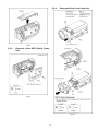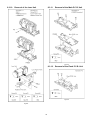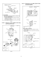
1
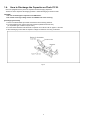
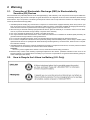
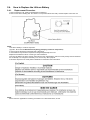
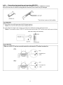
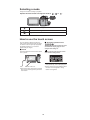
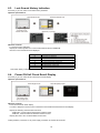
ORDER NO. VM1002005CE B27 High Definition Video Camera Model No. HDC-HS60P HDC-HS60PC HDC-HS60PU HDC-HS60EB HDC-HS60EC HDC-HS60EE HDC-HS60EF HDC-HS60EG HDC-HS60EP HDC-HS60GC HDC-HS60GK HDC-HS60GN HDC-HS60GT HDC-HS60SG Vol. 1 Colour (K)...........Black Type 4 © Panasonic Corporation 2010 Unauthorized copying and distribution is a violation of law. TABLE OF CONTENTS PAGE 1 Safety Precautions -----------------------------------------------3 1.1. General Guidelines ----------------------------------------3 1.2. Leakage Current Cold Check ---------------------------3 1.3. Leakage Current Hot Check (See Figure 1.)--------3 1.4. How to Discharge the Capacitor on Flash P.C.B.----------------------------------------------------------4 2 Warning --------------------------------------------------------------5 2.1. Prevention of Electrostatic Discharge (ESD) to Electrostatically Sensitive (ES) Devices ----------5 2.2. How to Recycle the Lithium Ion Battery (U.S. Only)-----------------------------------------------------------5 2.3. Caution for AC Cord (For EB/GC) ---------------------6 2.4. How to Replace the Lithium Battery -------------------7 3 Service Navigation------------------------------------------------8 3.1. Introduction --------------------------------------------------8 3.2. General Description About Lead Free Solder (PbF) ----------------------------------------------------------8 3.3. Important Notice 1 -----------------------------------------8 3.4. How to Define the Model Suffix (NTSC or PAL model)---------------------------------------------------------9 3.5. Precautions for Handling HDD------------------------ 10 3.6. Formatting-------------------------------------------------- 14 4 Specifications ---------------------------------------------------- 15 5 Location of Controls and Components------------------ 18 6 Service Mode ----------------------------------------------------- 21 6.1. Drive Information Display ------------------------------ 22 6.2. HDD Self Check Execution ---------------------------- 22 6.3. Lock Search History Indication ----------------------- 23 6.4. Power ON Self Check Result Display--------------- 23 6.5. HDD Hardware Test ------------------------------------- 24 7 Service Fixture & Tools --------------------------------------- 25 7.1. When Replacing the Main P.C.B. -------------------- 25 7.2. Service Position ------------------------------------------ 25 8 Disassembly and Assembly Instructions --------------- 27 8.1. Disassembly Flow Chart-------------------------------- 27 8.2. PCB Location---------------------------------------------- 27 8.3. Disassembly Procedure -------------------------------- 28 9 Measurements and Adjustments -------------------------- 42 9.1. Electric Adjustment -------------------------------------- 42 10 Factory Setting--------------------------------------------------- 44 10.1. How To Turn On The Factory Settings? ------------ 44 10.2. What Is The Factory Settings? ----------------------- 45 PAGE 2 1 Safety Precautions 1.1. General Guidelines 1.3. 1. IMPORTANT SAFETY NOTICE There are special components used in this equipment which are important for safety. These parts are marked by 2. 3. 4. 5. 1. Plug the AC cord directly into the AC outlet. Do not use an isolation transformer for this check. 2. Connect a 1.5 kΩ, 10 W resistor, in parallel with a 0.15 μF capacitor, between each exposed metallic part on the set and a good earth ground, as shown in Figure 1. 3. Use an AC voltmeter, with 1 kΩ/V or more sensitivity, to measure the potential across the resistor. 4. Check each exposed metallic part, and measure the voltage at each point. 5. Reverse the AC plug in the AC outlet and repeat each of the above measurements. 6. The potential at any point should not exceed 0.75 V RMS. A leakage current tester (Simpson Model 229 or equivalent) may be used to make the hot checks, leakage current must not exceed 1/2 mA. In case a measurement is outside of the limits specified, there is a possibility of a shock hazard, and the equipment should be repaired and rechecked before it is returned to the customer. in the Schematic Diagrams, Circuit Board Layout, Exploded Views and Replacement Parts List. It is essential that these critical parts should be replaced with manufacturer’s specified parts to prevent X-RADIATION, shock, fire, or other hazards. Do not modify the original design without permission of manufacturer. An Isolation Transformer should always be used during the servicing of AC Adaptor whose chassis is not isolated from the AC power line. Use a transformer of adequate power rating as this protects the technician from accidents resulting in personal injury from electrical shocks. It will also protect AC Adaptor from being damaged by accidental shorting that may occur during servicing. When servicing, observe the original lead dress. If a short circuit is found, replace all parts which have been overheated or damaged by the short circuit. After servicing, see to it that all the protective devices such as insulation barriers, insulation papers shields are properly installed. After servicing, make the following leakage current checks to prevent the customer from being exposed to shock hazards. 1.2. Leakage Current Hot Check (See Figure 1.) Leakage Current Cold Check 1. Unplug the AC cord and connect a jumper between the two prongs on the plug. 2. Measure the resistance value, with an ohmmeter, between the jumpered AC plug and each exposed metallic cabinet part on the equipment such as screwheads, connectors, control shafts, etc. When the exposed metallic part has a return path to the chassis, the reading should be between 1 MΩ and 5.2 MΩ. When the exposed metal does not have a return path to the chassis, the reading must be infinity. Figure. 1 3 1.4. How to Discharge the Capacitor on Flash P.C.B. • This unit equipped with two pieces of capacitors as flash charging capacitors. “Either one of the capacitor discharging operation” makes discharging for others as well. CAUTION: 1. Be sure to discharge the capacitor on FLASH P.C.B.. 2. Be careful of the high voltage circuit on FLASH P.C.B. when servicing. [Discharging Procedure] 1. Refer to the disassemble procedure and Remove the necessary parts/unit. 2. Put the insulation tube onto the lead part of Resistor (ERG5SJ102:1kΩ /5W). (an equivalent type of resistor may be used.) 3. Put the resistor between both terminals of capacitor on FLASH P.C.B. for approx. 5 seconds. 4. After discharging confirm that the capacitor voltage is lower than 10V using a voltmeter. Fig. F1 4 2 Warning 2.1. Prevention of Electrostatic Discharge (ESD) to Electrostatically Sensitive (ES) Devices Some semiconductor (solid state) devices can be damaged easily by static electricity. Such components commonly are called Electrostatically Sensitive (ES) Devices. Examples of typical ES devices are integrated circuits and some field-effect transistors and semiconductor "chip" components. The following techniques should be used to help reduce the incidence of component damage caused by electrostatic discharge (ESD). 1. Immediately before handling any semiconductor component or semiconductor-equipped assembly, drain off any ESD on your body by touching a known earth ground. Alternatively, obtain and wear a commercially available discharging ESD wrist strap, which should be removed for potential shock reasons prior to applying power to the unit under test. 2. After removing an electrical assembly equipped with ES devices, place the assembly on a conductive surface such as aluminum foil, to prevent electrostatic charge buildup or exposure of the assembly. 3. Use only a grounded-tip soldering iron to solder or unsolder ES devices. 4. Use only an antistatic solder removal device. Some solder removal devices not classified as "antistatic (ESD protected)" can generate electrical charge sufficient to damage ES devices. 5. Do not use freon-propelled chemicals. These can generate electrical charges sufficient to damage ES devices. 6. Do not remove a replacement ES device from its protective package until immediately before you are ready to install it. (Most replacement ES devices are packaged with leads electrically shorted together by conductive foam, aluminum foil or comparable conductive material). 7. Immediately before removing the protective material from the leads of a replacement ES device, touch the protective material to the chassis or circuit assembly into which the device will be installed. CAUTION : Be sure no power is applied to the chassis or circuit, and observe all other safety precautions. 8. Minimize bodily motions when handling unpackaged replacement ES devices. (Otherwise harmless motion such as the brushing together of your clothes fabric or the lifting of your foot from a carpeted floor can generate static electricity (ESD) sufficient to damage an ES device). 2.2. How to Recycle the Lithium Ion Battery (U.S. Only) 5 2.3. 2.3.1. Caution for AC Cord (For EB/GC) 2.3.2.1. Important The wires in this mains lead are coloured in accordance with the following code: Information for Your Safety Blue Brown IMPORTANT Your attention is drawn to the fact that recording of prerecorded tapes or discs or other published or broadcast material may infringe copyright laws. WARNING To reduce the risk of fire or shock hazard, do not expose this equipment to rain or moisture. CAUTION To reduce the risk of fire or shock hazard and annoying interference, use the recommended accessories only. FOR YOUR SAFETY DO NOT REMOVE THE OUTER COVER To prevent electric shock, do not remove the cover. No user serviceable parts inside. Refer servicing to qualified service Neutral Live As the colours of the wires in the mains lead of this appliance may not correspond with the coloured markings identifying the terminals in your plug, proceed as follows: The wire which is coloured BLUE must be connected to the terminal in the plug which is marked with the letter N or coloured BLACK. The wire which is coloured BROWN must be connected to the terminal in the plug which is marked with the letter L or coloured RED. personnel. 2.3.2. Under no circumstances should either of these wires be connected to the earth terminal of the three pin plug, marked with the letter E or the Earth Symbol. Caution for AC Mains Lead For your safety, please read the following text carefully. This appliance is supplied with a moulded three-pin mains plug for your safety and convenience. A 5-ampere fuse is fitted in this plug. Should the fuse need to be replaced please ensure that the replacement fuse has a rating of 5 amperes and it is approved by ASTA or BSI to BS1362 Check for the ASTA mark or the BSI mark on the body of the fuse. 2.3.2.2. Before Use Remove the Connector Cover as follows. If the plug contains a removable fuse cover you must ensure that it is refitted when the fuse is replaced. If you lose the fuse cover, the plug must not be used until a replacement cover is obtained. A replacement fuse cover can be purchased from your local Panasonic Dealer. 2.3.2.3. How to Replace the Fuse 1. Remove the Fuse Cover with a screwdriver. If the fitted moulded plug is unsuitable for the socket outlet in your home then the fuse should be removed and the plug cut off and disposed of safety. There is a danger of severe electrical shock if the cut off plug is inserted into any 13-ampere socket. If a new plug is to be fitted please observe the wiring code as shown below. If in any doubt, please consult a qualified electrician. 2. Replace the fuse and attach the Fuse cover. 6 2.4. 2.4.1. How to Replace the Lithium Battery Replacement Procedure 1. Remove the SD P.C.B.. (Refer to Disassembly Procedures.) 2. Remove the Lithium battery (Ref. No. “B6401” at component side of SD P.C.B.) and then replace it into new one. NOTE: This Lithium battery is a critical component. (Type No.: ML-614S/ZTK Manufactured by Energy Company, Panasonic Corporation) It must never be subjected to excessive heat or discharge. It must therefore only be fitted in requirement designed specifically for its use. Replacement batteries must be of same type and manufacture. They must be fitted in the same manner and location as the original battery, with the correct polarity contacts observed. Do not attempt to re-charge the old battery or re-use it for any other purpose. It should be disposed of in waste products destined for burial rather than incineration. NOTE: Above caution is applicable for a battery pack which is for HDC-HS60 series, as well. 7 3 Service Navigation 3.1. Introduction This service manual contains technical information, which allow service personnel’s to understand and service this model. Please place orders using the parts list and not the drawing reference numbers. If the circuit is changed or modified, the information will be followed by service manual to be controlled with original service manual. 3.2. General Description About Lead Free Solder (PbF) The lead free solder has been used in the mounting process of all electrical components on the printed circuit boards used for this equipment in considering the globally environmental conservation. The normal solder is the alloy of tin (Sn) and lead (Pb). On the other hand, the lead free solder is the alloy mainly consists of tin (Sn), silver (Ag) and Copper (Cu), and the melting point of the lead free solder is higher approx.30°C (86°F) more than that of the normal solder. Distinction of P.C.B. Lead Free Solder being used Service caution for repair work using Lead Free Solder (PbF) • The lead free solder has to be used when repairing the equipment for which the lead free solder is used. (Definition: The letter of “PbF” is printed on the P.C.B. using the lead free solder.) • To put lead free solder, it should be well molten and mixed with the original lead free solder. • Remove the remaining lead free solder on the P.C.B. cleanly for soldering of the new IC. • Since the melting point of the lead free solder is higher than that of the normal lead solder, it takes the longer time to melt the lead free solder. • Use the soldering iron (more than 70W) equipped with the temperature control after setting the temperature at 350±30°C (662±86°F). Recommended Lead Free Solder (Service Parts Route.) • The following 3 types of lead free solder are available through the service parts route. RFKZ03D01KS-----------(0.3mm 100g Reel) RFKZ06D01KS-----------(0.6mm 100g Reel) RFKZ10D01KS-----------(1.0mm 100g Reel) Note * Ingredient: tin (Sn) 96.5%, silver (Ag) 3.0%, Copper (Cu) 0.5%, Cobalt (Co) / Germanium (Ge) 0.1 to 0.3% 3.3. Important Notice 1 1. The service manual does not contain the following information, because of the impossibility of servicing at component level without concerned equipment/facilities. a. Schematic diagram, Block Diagram and P.C.B. layout of MAIN P.C.B.. b. Parts list for individual parts for MAIN P.C.B.. When a part replacement is required for repairing MAIN P.C.B., replace as an assembled parts. (Main P.C.B.) 2. The following category is /are recycle module part. Please send it/them to Central Repair Center. • MAIN P.C.B. (VEP03H84AN: HDC-HS60P/PC/PU/GT) • MAIN P.C.B. (VEP03H84AP: HDC-HS60EB/EC/EF/EG/EP) • MAIN P.C.B. (VEP03H84AQ: HDC-HS60EE/GC/GKGN/SG) 8 3.4. How to Define the Model Suffix (NTSC or PAL model) There are seven kinds of HDC-HS60. • a) HDC-HS60P • b) HDC-HS60PC • c) HDC-HS60EB/EC/EF/EG/EP/GN • d) HDC-HS60EE • e) HDC-HS60GK • f) HDC-HS60GT • g) HDC-HS60PU/GC/SG What is the difference is that the “INITIAL SETTING” data which is stored in Flash ROM mounted on Main P.C.B.. 3.4.1. Defining methods: To define the model suffix to be serviced, refer to the rating label which is putted on the Unit. NOTE: After replacing the MAIN P.C.B., be sure to achieve adjustment. The adjustment instruction is available at “software download” on the “Support Information from NWBG/VDBG-AVC” web-site in “TSN system”, together with Maintenance software. 9 3.5. Precautions for Handling HDD 1. Handle HDD very carefully to prevent the static electricity and shock. 2. Set the HDD quickly after taking it out from the package. Make sure to put the HDD on buffer materials, etc. 3.5.1. Precautions at incoming process and for opening packages 10 3.5.2. Precautions for installing HDD 11 3.5.3. Precautions for inserting and removing HDD FPC Make sure to use the tool (LSVQ0112) when locking and unlocking the lock lever of HDD FPC connector. Do not lock the lock lever without inserting HDD FPC. Otherwise, the connector may be damaged. 12 Make sure to use the tool (LSVQ0112) when opening and closing the lock lever. When install the HDD to main unit, necessary install the HDD FPC and HDD cushion. 13 3.6. Formatting 14 4 Specifications 15 16 17 5 Location of Controls and Components 1 2 34 5 1 2 3 5 6 7 Power button [ ] Speaker Intelligent auto/Manual button [iA/MANUAL] Optical image stabilizer button [ /O.I.S.] Mode switch Battery holder HDMI mini connector [HDMI] 8 9 USB terminal [ ] AV multi connector [AV MULTI] 4 AV MULTI 7 8 9 6 10 11 12 Use the AV multi cable (only the supplied cable). 10 SD card cover 11 Card slot 12 Access lamp [ACCESS] 13 Lens cover The lens cover opens in Motion Picture Recording Mode or Still Picture Recording Mode. 14 Internal stereo microphones 15 Built-in flash 16 Lens 17 Video light 13 14 15 16 17 18 19 18 LCD monitor (Touch screen) ● It can open up to 90Q. ● It can rotate up to 180Q towards the lens or 90Qtowards the opposite direction. 20 21 22 2324 Due to limitations in LCD production technology, there may be some tiny bright or dark spots on the LCD monitor screen. However, this is not a malfunction and does not affect the recorded picture. 19 Recording start/stop button 20 Sub recording start/stop button ● This button functions in the same manner as the recording start/stop button. 21 Adjust zoom buttons 22 Menu button [MENU] 23 Video light button [LIGHT] 24 Delete button [ ] 18 25 Tripod receptacle 26 Battery release lever [BATTERY] 25 26 27 Status indicator 28 Photoshot button [ ] 29 Zoom lever [W/T] (In Motion Picture Recording Mode or Still Picture Recording Mode) Thumbnail display switch [ / ]/ Volume lever [UVOLT] (In Playback Mode) 30 HDD access lamp [ACCESS HDD] 31 DC input terminal ● Do not use any other AC adaptors except the supplied one. 32 Grip belt 27 28 29 30 32 31 Flip the belt. Adjust the length. Replace the belt. 19 Selecting a mode Change the mode to recording or playback. Operate the mode switch to change the mode to , or . Motion Picture Recording Mode Still Picture Recording Mode Playback Mode How to use the touch screen You can operate by directly touching the LCD monitor (touch screen) with your finger. It is easier to use the stylus pen (supplied) for detailed operation or if it is hard to operate with your fingers. ■ About the operation icons / / / : These icons are used to switch the menu and thumbnail display page, for item selection and setting etc. ■ Touch : Touch to return to the previous screen such as when setting menus Touch and release the touch screen to select icon or picture. Do not touch on the LCD monitor with hard pointed tips, such as ball point pens. ● Perform the touch screen calibration when the touch is not recognized or wrong location is recognized. ● ● ● Touch the center of the icon. Touching the touch screen will not operate while you are touching another part of the touch screen. 20 6 Service Mode 1. Indication method of the service menu Set the mode dial “Motion Picture Recording” mode. 2. Turn the power on, and then while keep pressing the "Zoom lever" to W side, "Intelligent auto/Manual" button and "Menu" button for more than 3 seconds until the top screen of the Service Mode Menu being displayed. Service mode menu Screen display 1 Contents Factory settings 2 Drive information display 3 4 5 HDD self check execution Lock search history indication Power ON self check result display 6 HDD hardware test Function Function to throw a product up in a factory shipment state (When recorded data in HDD, “error display” is done) Fall detection frequency of HDD, Frequency that exceeds highest/lowest operation guarantee temperature and serial number display Function to check self as for the state of HDD Display an error cord for three histories saved in EEPROM Power ON self check (function to diagnose correct function of the device and interface between devices) result display Function to confirm state of HDD hardware NOTE: Do not using service mode except above table of Service Menu. 3. End method of the top screen of the service menu Push the menu button to end the service mode, and then POWER OFF. 21 6.1. Drive Information Display Touch the [ 2 ] of LCD, select Drive Information display. Operation specifications Indication contents • Drive Information display Display the fall detection frequency of HDD, Frequency that exceeds highest/lowest operation guarantee temperature and serial number. Push the menu button to end the service mode, and then POWER OFF. 6.2. HDD Self Check Execution Touch the [ 3 ] of LCD, select HDD self check execution. Operation specifications Indication contents • HDD self check execution Display the HDD self check result information. Displays other than “OK” are abnormalities of HDD. Push the menu button to end the service mode, and then POWER OFF. 22 6.3. Lock Search History Indication Touch the [ 4 ] of LCD, select Lock search history indication. Operation specifications Indication contents • Lock search history indication Display the camera system error cord for three histories saved in EEPROM. • The error cord contents which are displayed Error code 51 52 53 71 72 73 33 Function Focus control is abnormal Zoom control is abnormal OIS lens control is abnormal Lens cover open/close is abnormal Cooling fan is abnormal High temperature is abnormal Communication between camera to ARM is abnormal Lock search history indication is finished by POWER OFF. 6.4. Power ON Self Check Result Display Touch the [ 5 ] of LCD, select Power ON self check result display. Operation specifications Indication contents • Power ON self check result display Function to diagnose correct function of the device and interface between devices result display. Display the following commnucation test result. - CAM-PWR : Commnucation test between IC2006 to IC301 - CAM-UNI : Commnucation test between IC3401 to IC301 Display other than “OK” are abnomalities of each lines. Cutting of battery connection or AC power supply connection to end the service mode. 23 6.5. HDD Hardware Test Touch the [ 6 ] of LCD, select HDD hardware test. Operation specifications Indication contents • HDD hardware test Display the HDD hardware test result information. • The error cord contents which are displayed Error code NO ERROR CTR ERROR BUFF RAM ERROR ECC DEV ERROR CPU ERROR COMMAND ERROR Function It is normal without the error Controller Resistor Error Buffer RAM Error ECC device Error CPU RAM/ROM Error Reserved In the above table, displays other than “NO ERROR” are abnormalities of HDD. Push the menu button to end the service mode, and then POWER OFF. 24 7 Service Fixture & Tools 7.1. When Replacing the Main P.C.B. After replacing the MAIN P.C.B., be sure to achieve adjustment. The adjustment instruction is available at “software download” on the “Support Information from NWBG/VDBG-AVC” web-site in “TSN system”, together with Maintenance software. 7.2. Service Position This Service Position is used for checking and replacing parts. Use the following Extension cables for servicing. Table S1 Extension Cable List No. 1 2 3 4 5 6 7 8 Parts No. RFKZ0379 RFKZ0448 VFK1933 RFKZ0343 RFKZ0379 VFK1480 VFK1933 VFK1286 Connection PP6006(MAIN) - HDD FPC FP6008(MAIN) - LENS UNIT PP6004(MAIN) - MONITOR FPC PP6002(MAIN) - PS7001(FLASH) PS6002(MAIN) - PP6401(SD) FP6001(MAIN) - FP6501(SIDE (R) OP) PP6003(MAIN) - PS6701(POWER FPC) FP7001(FLASH) - FRONT CASE UNIT 25 Form 40PIN 0.5 B to B 33PIN 0.3 FPC 34PIN 0.5 B to B 30PIN 0.5 B to B 40PIN 0.5 B to B 6PIN 0.5 FFC 34PIN 0.5 B to B 16PIN 0.5 FFC CAUTION-1. (When servicing FLASH P.C.B.) 1. Be sure to discharge the capacitor on FLASH P.C.B.. Refer to “HOW TO DISCHARGE THE CAPACITOR ON FLASH P.C.B.”. The capacitor voltage is not lowered soon even if the AC Cord is unplugged or the battery is removed. 2. Be careful of the high voltage circuit on FLASH P.C.B.. 3. DO NOT allow other parts to touch the high voltage circuit on FLASH P.C.B.. 26 8 Disassembly and Assembly Instructions 8.1. Disassembly Flow Chart This is a disassembling chart. When assembling, perform this chart conversely. 8.2. PCB Location 27 8.3. Disassembly Procedure No. Item 1 R Cover Unit Fig Fig.D1 Fig.D2 2 Side Case (L) Unit Fig.D3 Fig.D4 3 HDD Unit Fig.D5 Fig.D6 4 Top Case Fig.D7 5 HDD Shield Frame Unit Front Case Unit 6 7 Side Case (R) Unit Fig.D8 Fig.D9 Fig.D10 Fig.D11 8 Switch Unit (Top)/ Batt Case Unit Fig.D12 9 SD Frame Fig.D13 10 11 12 13 Lens Unit Main P.C.B. Unit Flash P.C.B. Unit Switch Unit (Top) Power FPC Unit Fig.D14 Fig.D15 Fig.D16 Fig.D17 Fig.D18 Removal 2 Screws (A) 1 Screw (B) 3 Locking tabs R Cover Unit 6 Screws (C) 5 Locking tabs Side Case (L) Unit PP6006 (Connector) 2 HDD Cushions HDD Unit 1 Screw (D) 2 Screws (E) 2 Ribs Top Case 2 Screws (F) HDD Shield Frame Unit 1 Screw (G) 1 Screw (H) Front Under Cover 1 Locking tab 2 Ribs P7001 (Connector) P7002 (Connector) FP7001 (Flex) Front Case Unit 1 Screw (I) 1 Screw (J) 1 Screw (K) 2 Screws (L) 1 Rib 2 Locking tabs FP6501 (Flex) PP6004 (Connector) Side Case (R) Unit 1 Screw (M) 2 Locking tabs Switch Unit (Top)/ Batt Case Unit 2 Screws (N) PP6401 (Connector) SD Frame 1 Screw (O) 1 Rib P6001 (Connector) FP6008 (Flex) 1 Screw (P) 1 Screw (Q) Lens Frame R Unit Radiation Plate Unit Lens Unit 3 Screws (R) PP6002 (Connector) Main P.C.B. Unit 2 Screws (S) Flash P.C.B. Unit Discharge of the Capacitor FP6701 (Flex) 2 Screws (T) 6 Ribs Switch Unit (Top) Power FPC Unit No. Item 14 Side (R) OP P.C.B. Unit Speaker Fig Fig.D19 15 LCD Case Unit Fig.D20 16 Monitor P.C.B. Unit Fig.D21 Fig.D22 Fig.D23 28 17 Barrier Motor Fig.D24 18 Front P.C.B. Unit Fig.D25 19 Lens Damper Barrier Lever Barrier Change Lever Fig.D26 20 ECM FPC Unit Fig.D27 21 MOS Unit IR Filter Fig.D28 22 IRIS Unit Fig.D29 23 Focus Motor Fig.D30 Fig.D31 24 Zoom Motor Fig.D32 25 1st Lens Frame Unit Reinforcement Plate Fig.D33 26 2nd Lens Frame Move Fig.D34 Unit Removal 2 Screws (U) 1 Screw (V) P6501 (Connector) SP Angle Side (R) OP P.C.B. Unit Speaker 2 Screws (W) Switch Unit Light Guide Plate Earth Plate 3 Ribs LCD Case Unit FP904 (Flex) FP905 (Flex) 2 Ribs LCD Frame FP903 (Flex) 4 Locking tabs Monitor P.C.B. Unit 1 Locking tab Reflection Sheet Light Guide Plate Diffusion Sheet Prism Sheet B Prism Sheet A Lens Holder Monitor P.C.B. Unit 1 Screw (Z) 4 Screws (a) Front Frame FP6600 (Flex) Barrier Motor 1 Screw (b) FP6601 (Flex) Front P.C.B. Unit 2 Barrier Springs LED Light Lens 2 Locking tabs Lens Damper Barrier Lever Barrier Change Lever 1 Screw (c) 2 Locking tabs Front Base ECM FPC Unit 2 Screws (d) MOS Cushion MOS Unit IR Filter 20 Points Solder 3 Screws (e) 2 Ribs IRIS Unit 1 Screw (f) Focus Motor 2 Screws (g) Zoom Motor 3 Screws (h) 2 1st Lens Frame Springs 3 Screws (i) 1st Lens Frame Unit Reinforcement Plate 2nd Lens Frame Move Unit No. Item 27 Body Unit 28 29 Fig Fig.D35 Zoom Guide Pole Fig.D36 OIS Unit 4th Lens Frame Move Fig.D37 Unit Focus Guide Pole L Removal 3 Screws (j) Body Unit 2 Zoom Guide Poles OIS Unit 4th Lens Frame Move Unit 2 Focus Guide Poles L Fig.D2 8.3.2. 8.3.1. Removal of the Side Case (L) Unit Removal of the R Cover Unit Fig.D3 Fig.D1 29 Fig.D6 8.3.4. Removal of the Top Case Fig.D4 8.3.3. Removal of the HDD Unit Fig.D7 Fig.D5 30 8.3.6. Removal of the Front Case Unit Fig.D8 8.3.5. Removal of the HDD Shield Frame Unit Fig.D9 Fig.D10 31 8.3.7. Removal of the Side Case (R) Unit 8.3.8. Removal of the Switch Unit (Top)/ Batt Case Unit Fig.D12 8.3.9. Removal of the SD Frame Fig.D13 Fig.D11 32 8.3.10. Removal of the Lens Unit 8.3.11. Removal of the Main P.C.B. Unit Fig.D15 8.3.12. Removal of the Flash P.C.B. Unit Fig.D16 Fig.D14 33 8.3.14. Removal of the Side (R) OP P.C.B. Unit and Speaker Fig.D17 8.3.13. Removal of the Switch Unit (Top) and Power FPC Unit Fig.D19 Fig.D18 34 8.3.15. Removal of the LCD Case Unit 8.3.16. Removal of the Monitor P.C.B. Unit Fig.D21 Fig.D20 35 Fig.D22 Fig.D23 36 8.3.17. Removal of the Barrier Motor 8.3.18. Removal of the Front P.C.B. Unit Fig.D25 8.3.19. Removal of the Lens Damper, Barrier Lever and Barrier Change Lever Fig.D26 Fig.D24 37 8.3.20. Removal of the ECM FPC Unit 8.3.21. Removal of the MOS Unit and IR Filter Fig.D28 8.3.22. Removal of the IRIS Unit Fig.D27 Fig.D29 38 8.3.24. Removal of the Zoom Motor Fig.D30 8.3.23. Removal of the Focus Motor Fig.D32 Fig.D31 39 8.3.25. Removal of the 1st Lens Frame Unit and Reinforcement Plate 8.3.26. Removal of the 2nd Lens Frame Move Unit Fig.D34 8.3.27. Removal of the Body Unit Fig.D33 Fig.D35 40 8.3.28. Removal of the Zoom Guide Pole and OIS Unit Fig.D36 8.3.29. Removal of the 4th Lens Frame Move Unit and Focus Guide Pole L Fig.D37 41 9 Measurements and Adjustments 9.1. • • • • Electric Adjustment Adjustment method is different from a conventional High definition video camera. An exclusive jig and PC (including software for adjustment “Tatsujin”) are necessary for electric adjustment. A USB driver for service is necessary to communication with PC. Connection method of the main unit and an exclusive adjustment jig as follows 9.1.1. Adjustment Procedure • Connect the main unit to PC with USB. The adjustment instruction is available at "Software download" on the "Support Information from NWBG/VDBG-AVC" web-site in "TSN System". Figure of connection Figure of image when adjustment Part Number of jig • Only a necessary jig mentions it in setup of electric adjustment. No. 1 2 3 4 Part Name PC AC Adaptor USB Cable Adjustment Software (Tatsujin) Part Number --------------------- 42 Remarks Adjustment Items • Adjustment item as follows. The adjustment instruction is available at "Software download" on the "Support Information from NWBG/VDBG-AVC" web-site in "TSN System". 43 10 Factory Setting 10.1. How To Turn On The Factory Settings? 1. Set the mode switch “Motion Picture Recording” mode. 2. Turn the power on, and then while keep pressing the “Zoom lever” to W side, “Intelligent auto/Manual” button and “Menu” button for more than 3 seconds until the top screen of the Service Mode Menu being displayed. 3. Touch the [ 1 ] of LCD. 4. Touch the [ YES ] of LCD. 5. After few seconds “END” is displayed on LCD monitor. Cutting of battery connection or AC power supply connection as a completion of the “FACTORY SETTINGS”. 44 10.2. What Is The Factory Settings? The factory settings clean up and/or refresh the following settings. 1. MENU, MODE, ADJUSTMENT VALUE. 2. SD card format. 3. Reset the folder number and file number of still pictures. (Setting the folder number is 100, and file number is 0.) 4. Clear the mechanism lock information. 5. Clear the service mode information contents. 6. Close the lens cover 7. Initialize the VIERA Link Physical Address. 8. Confirm the data area of HDD is cleared. (When recorded data in HDD, "error display" is done) If "error display" is done, execute physical format according to the following procedure. The setting position of factory settings: Name Mode switch Setting position Motion picture recording mode 45 VM1002005CE Service Manual S1.1. Important Safety Notice Diagrams and Replacement Parts List High Definition Video Camera Model No. HDC-HS60P HDC-HS60PC HDC-HS60PU HDC-HS60EB HDC-HS60EC HDC-HS60EE HDC-HS60EF HDC-HS60EG HDC-HS60EP HDC-HS60GC HDC-HS60GK HDC-HS60GN HDC-HS60GT HDC-HS60SG S1. About Indication of The Schematic Diagram COMPONENTS IDENTIFIED WITH THE MARK HAVE THE SPECIAL CHARACTERISTICS FOR SAFETY. WHEN REPLACING ANY OF THESE COMPONENTS USE ONLY THE SAME TYPE. 1.Although reference number of the parts is indicated on the P.C.B. drawing and/or schematic diagrams, it is NOT mounted on the P.C.B. when it is displayed with "$" mark. 2.It is only the "Test Round" and no terminal (Pin) is available on the P.C.B. when the TP (Test Point) indicated as " " mark. 3.The voltage being indicated on the schematic diagram is measured in "Standard-Playback" mode when there is no specify mode is mentioned. 4.Although the voltage and waveform available on here is measured with standard frame, it may be differ from actual measurement due to modification of circuit and so on. 5.The voltage being indicated here may be include observational-error (deviation) due to internal-resistance and/or reactance of equipment. Therefore, handle the value indicated on here as reference. 6.Use the parts number indicated on the Replacement Parts List . 7.Indication on Schematic diagrams: Circuit name being connected. Vol. 1 Colour (K)...........Black Type OFTR FEP Name of Signal Table of contents S1. About Indication of The Schematic Diagram............................. S-1 S1.1. Important Safety Notice......................................................... S-1 S2. Voltage Chart............................................................................ S-2 S2.1. Strobe P.C.B........................................................................... S-2 S2.2. Front P.C.B............................................................................. S-2 S2.3. SD P.C.B................................................................................ S-2 S3. Block Diagram........................................................................... S-3 S3.1. Overall Block Diagram........................................................... S-3 S4. Schematic Diagram................................................................... S-4 S4.1. Interconnection Diagram........................................................ S-4 S4.2. Strobe Schematic Diagram.................................................... S-5 S4.3. Front Schematic Diagram...................................................... S-6 S4.4. SD Schematic Diagram.......................................................... S-7 S4.5. Side R Schematic Diagram.................................................... S-8 S4.6. Monitor Schematic Diagram................................................... S-9 S4.7. Power FPC Schematic Diagram.......................................... S-10 S4.8. HDD FPC Schematic Diagram............................................. S-11 S5. Print Circuit Board................................................................... S-12 S5.1. Strobe P.C.B......................................................................... S-12 S5.2. Front P.C.B........................................................................... S-13 S5.3. SD P.C.B.............................................................................. S-14 S5.4. Side R P.C.B........................................................................ S-14 S5.5. Monitor P.C.B....................................................................... S-15 S5.5.1. Monitor P.C.B. (Component Side)..................................... S-15 S5.5.2. Monitor P.C.B. (Foil Side).................................................. S-16 S5.6. Power FPC P.C.B................................................................. S-17 S5.7. HDD FPC P.C.B................................................................... S-18 S6. Replacement Parts List........................................................... S-19 S7. Exploded View........................................................................ S-27 S7.1. Frame and Casing Section (1)............................................. S-27 S7.2. Frame and Casing Section (2)............................................. S-28 S7.3. LCD Section......................................................................... S-29 S7.4. Camera Lens Section.......................................................... S-30 S7.5. Packing Parts and Accessories Section............................... S-31 S-1 This signal is connected to the FEP schematic diagram. S2. Voltage Chart Note) Indicated voltage values are the standard values for the unit measured by the DC electronic circuit tester (high-impedance) with the chassis taken as standard. Therefore, there may exist some errors in the voltage values, depending on the internal impedance of the DC circuit tester. S2.1. Strobe P.C.B. REF No. IC4801 IC4801 IC4801 IC4801 IC4801 IC4801 IC4801 IC4801 IC7001 IC7001 IC7001 IC7001 IC7001 IC7001 IC7001 IC7001 IC7001 IC7001 Q4801 Q4801 Q4801 PIN No. 1 2 3 4 5 6 7 8 1 2 3 4 5 6 7 8 9 10 E C B POWER ON 2.6 2.6 2.6 0 2.6 2.6 2.6 5 0 0 0 0 3.2 0 0 0 2.9 4.6 4.3 5 5 S2.2. Front P.C.B. REF No. Q6622 Q6622 Q6622 Q6623 Q6623 Q6623 PIN No. E C B E C B POWER ON 0 2.9 0 0 0 0 S2.3. SD P.C.B. REF No. IC6402 IC6402 IC6402 IC6402 IC6402 Q3901 Q3901 Q3901 QR6402 QR6402 QR6402 PIN No. 1 2 3 4 5 E C B E C B POWER ON 3.2 0 0 2.9 3.2 3.2 3.2 3.2 2.9 -0.5 2.9 S-2 S3. Block Diagram S3.1. Overall Block Diagram NOTE : VIDEO SIGNAL : AUDIO SIGNAL SHUTTER : CLK or CONTROL LINE LENS(F1.8-3.3 25x) ZOOM/ FOCUS MOTOR/ OIS IC201 MOS IMAGE SENSOR IRIS/ ND Analog COLOR LCD PANEL X301 OSC (42.725275MHz) IC701 LENS/OIS DRIVE Analog A/V MULTI TERMINAL Analog Analog IC301 CAMERA DSP (LUPINAS) IC6401 GYRO SENSOR IC3701 AVIO CLK74M IC3401 MPEG CODEC (UNI PHIER XP) IC4801 MAIC AMP Analog ECM Analog SPEAKER IC3801 HDMI LSI FLASH HDMI mini CONNECTOR IC7001 FLASH CHARGE CONTROL IC2006 SYSTEM CONTROL (CAMERA MICROCOMPUTER) OPERATION CLK13M IC3403 PLL IC3402 NAND FLASH ROM/ 512Mbit CLK12M IC3301 G SENSOR IC2002 EEPROM HDD 120GB DC IN BATTERY IC1501-1505 CHARAGE CIRCUIT IC1001 POWER CIRCUIT IC2304 RTC X2301 (32.768kHz) SD CARD USB TERMINAL HDC-HS60 OVERALL BLOCK DIAGRAM S-3 1 2 3 4 5 6 7 8 9 10 11 12 S CK SEL1 TP S CS SEL2 TP S S2T Y TPNL S T2S X TPNL KEYIN 6 PW LCDBL H PW LCDBL L D GND D GND D GND D GND D GND FP902 MONITOR P.C.B. (FOIL SIDE) 1 2 3 4 5 6 7 8 9 10 11 12 13 14 15 16 CLK18 LCD PW REG1R8V BUS9 LCDYC0 BUS9 LCDYC1 BUS9 LCDYC2 BUS9 LCDYC3 BUS9 LCDYC4 BUS9 LCDYC5 BUS9 LCDYC6 BUS9 LCDYC7 BUS9 LCD H BUS9 LCD V PW REG3V S DO LCD S CS LCD S CLK LCD FP901 2 4 6 8 10 12 14 16 18 20 22 24 26 28 30 32 34 36 38 40 VGL2 VCC1 VCOMH IOVCC SDI CS DB1 DB3 DB5 DB7 VSYNC GND VCL C13P C11M C12M VCI1 VGH C22M C21M 1 3 5 7 9 11 13 15 17 19 21 23 25 27 29 31 33 35 37 39 41 GND GND VDD VCOML SDO SCL DB0 DB2 DB4 DB6 HSYNC DCLK VREG C13M DDVDH C11P C12P VCC2 C22P C21P VGL1 D GND POWER SW SPOUT1 SPOUT1 SPOUT2 SPOUT2 1 2 MONITOR FPC 6 5 4 3 2 1 LCD OP FPC P6501 SPOUT1 SPOUT2 : (FOIL SIDE) 1 2 3 4 5 6 FLASH P.C.B. (COMPONENT SIDE) 4 3 2 1 FP905 Y TOP X LEFT Y BOT X RIGHT SPOUT2 SPOUT2 SPOUT1 SPOUT1 POWER SW D GND PP6002 : (COMPONENT SIDE) HDD FPC OPERATION SW TOUCH PANEL S-4 TEMP GND TEMP OUT HDD3R3V DASP CS0 DA0 INTRQ HDD GND HDD GND DIOW DMARQ ATADATA15 ATADATA14 ATADATA13 ATADATA12 ATADATA11 ATADATA10 ATADATA9 ATADATA8 HDD GND 2 4 6 8 10 12 14 16 18 20 22 24 26 28 30 32 ZAP ZAN PIT DRV+ PIT HO+ PIT HOYAW DRV+ YAW HO+ YAW HOFABS T OUT ZABS IR HINIR HIN+ IR M+ FBN FBP MCLK A1.8V A1.8V RSTN SI HD SCK SCS VD DOEP DOEM DODP DODM DCKP DCKM DOCP DOCM DOBP DOBM D2.7V P6001 FP6008 20 19 18 17 16 15 14 13 12 11 10 9 8 7 6 5 4 3 2 1 ZBN 1 ZBP 3 PIT DRV5 PIT HIN7 PIT HIN+ 9 YAW DRV11 YAW HIN+ 13 YAW HIN15 17 FLED CONT FENC VCC 19 21 ZENC VCC & T VCC 23 ZLED CONT IR HOUT25 IR HOUT+ 27 IR M29 FAN 31 FAP 33 MAIN P.C.B. (FOIL SIDE) 40 39 38 37 36 35 34 33 32 31 30 29 28 27 26 25 24 23 22 21 PP6006 PS6001 1 TEMP VCC 2 HDD 3R3V 3 HDD UNLOAD 4 CS1 5 DA2 6 DA1 7 DMACK 8 IORDY 9 DIOR 10 HDD GND 11 HDD GND 12 ATADATA0 13 ATADATA1 14 ATADATA2 15 ATADATA3 16 ATADATA4 17 ATADATA5 18 ATADATA6 19 ATADATA7 20 RESET S CK SEL1 TP S CS SEL2 TP S S2T Y TPNL S T2S X TPNL KEYIN6 D GND D GND D GND D GND D GND D GND LCD OPEN LCD RVS PW REG3V S DO LCD S CS LCD S CLK LCD D GND TRIG P7002 UARTO UARTI PW REG5V E CAM RST OCD SDA OCD SCL TRACECLK TRACESYNC TRACEPKT0 TRACEPKT1 TRACEPKT2 TRACEPKT3 TRACEPKT4 S AMMPTXD G XP2 RST 17 16 15 14 13 12 11 10 9 8 7 6 5 4 3 2 1 1 2 P7001 XENON+ XENON1 2 3 4 5 6 7 8 9 10 11 12 13 14 15 PP6004 FLASH 30 TRACEPKT7 29 TRACEPKT6 28 TRACEPKT5 27 AFST 26 GND 25 BUS8 TRST 24 BUS8 TDI 23 BUS8 TMS 22 CLK16 TCK 21 BUS8 EXTRGO 20 BUS15 TDO 19 MVD 18 GLVD 17 GND 16 S AMMPRXD PW LCD BL H PW LCD BL L D GND D GND D GND CLK18 LCD PW REG1R8V BUS9 LCDYC0 BUS9 LCDYC1 BUS9 LCDYC2 BUS9 LCDYC3 BUS9 LCDYC4 BUS9 LCDYC5 BUS9 LCDYC6 BUS9 LCDYC7 BUS9 LCD H BUS9 LCD V D GND D GND PW STNOREG PW STNOREG PW STNOREG IGBT GND IGBT GND PW 3R2V TRIGEND CHAEND CHARGE S HDD G SCL S HDD G SDA D GND D GND D GND D GND PW STNOREG PW STNOREG PW STNOREG IGBT GND IGBT GND PW 3R2V TRIGEND CHAEND CHARGE S HDD G SCL S HDD G SDA D GND D GND 15 14 13 12 11 10 9 8 7 6 5 4 3 2 1 2 1 1 2 3 4 5 6 7 8 9 10 11 12 13 14 15 16 17 18 19 20 SD CLK SD GND SD DATA1 SD DATA0 SD DATA3 SD DATA2 SD GND SD CMD SD GND S HDD G SDA S HDD G SCL PW SD3R2V PW SD3R2V PW SD3R2V PW 3R2V PW REG3V SD GND G GYROP G GYRO REF G GYROY 1 2 3 4 5 6 7 8 9 10 11 12 13 14 15 16 17 40 39 38 37 36 35 34 33 32 31 30 29 28 27 26 25 24 23 22 21 PS6002 PHOTO SW PW REG3V ZOOM AD D GND BATT+ BATT+ BATT+ BATT+ BATT+ BATTBATTBATTBATTBATTBATTBATTBATT- 1 SD CLK 2 SD GND 3 SD DATA1 4 SD DATA0 5 SD DATA3 6 SD DATA2 7 SD GND 8 SD CMD 9 SD GND 10 S HDD G SDA 11 S HDD G SCL 12 PW SD3R2V 13 PW SD3R2V 14 PW SD3R2V 15 PW 3R2V 16 PW REG3V 17 SD GND 18 G GYROP 19 G GYRO REF 20 G GYROY NOREG GND NOREG GND NOREG GND NOREG GND NOREG GND E CARD DET A TEMP OUT PW LI BATT GYRO GND GYRO GND NOREG NOREG NOREG NOREG NOREG NOREG NOREG E CARD PRO LED HDD ACCESS CARD LED 40 NOREG GND 39 NOREG GND 38 NOREG GND 37 NOREG GND 36 NOREG GND 35 E CARD DET A 34 HDD TEMP 33 PW LI BATT 32 GYRO GND 31 GYRO GND 30 NOREG 29 NOREG 28 NOREG 27 NOREG 26 NOREG 25 NOREG 24 NOREG 23 E CARD PRO A 22 LED HDD ACCESS 21 CARD LED B EVR FP6001 15 14 13 12 11 10 9 8 7 6 5 4 3 2 1 NC LIGHT ON H PW 5V PW 5V LENSBA OPEN OP LED LENSBA MT ALENSBA MT BLENSBA MT A+ LENSBA MT B+ MIC GND MIC GND G MIC OUT R G MIC OUT L PW REG3V LENS BARRIER FP6501 NC LIGHT ON H PW 5V PW 5V LENSBA OPEN OP LED LENSBA MT ALENSBA MT BLENSBA MT A+ LENSBA MT B+ MIC GND MIC GND G MIC OUT R G MIC OUT L PW REG3V 18 19 20 21 22 23 24 25 26 27 28 29 30 31 32 33 34 16 17 18 19 20 21 22 23 24 25 26 27 28 29 30 16 17 18 19 20 21 22 23 24 25 26 27 28 29 30 PS7001 8 7 6 5 4 3 2 1 1 2 3 4 5 6 7 8 9 10 11 12 13 14 15 16 FP6603 1 2 3 4 LENSBA MT B+ LENSBA MT A+ LENSBA MT BLENSBA MT AOP LED D GND D GND SHTR OPEN ECM[L] GND[L] GND[R] ECM[R] FP6601 PW REG5V PW REG5V NC LIGHT ON H D GND D GND SHTER OPEN OP LED LENSBA MT ALENSBA MT BLENSBA MT A+ LENSBA MT B+ G ECMR MIC GND MIC GND G ECML ECM FPC FP903 PW REG3V KEYIN6 D GND D GND FP7001 PW REG5V PW REG5V NC LIGHT ON H D GND D GND SHTER OPEN OP LED LENSBA MT ALENSBA MT BLENSBA MT A+ LENSBA MT B+ G ECMR MIC GND MIC GND G ECML FRONT P.C.B. (FOIL SIDE) 1 2 3 4 1 2 3 4 5 6 7 8 9 10 11 12 13 14 15 16 S4. Schematic Diagram S4.1. Interconnection Diagram MIC MOS UINT FP6600 LENS UNIT MOS FPC SD HOLDER P.C.B. (FOIL SIDE) PP6401 PP6003 34 POWER LED 33 STANDBY LED E KEYIN1 32 E KEYIN4 31 BATT+ 30 BATT+ 29 BATT+ 28 BATT+ 27 BATT+ 26 T 25 D 24 BATT23 BATT22 BATT21 BATT20 BATT19 BATT18 SIDE-R OP FPC SPEAKER POWER FPC OPERATION SW HDD BATTERY LCD UNIT SIDE-R OP P.C.B. (FOIL SIDE) FP904 HDC-HS60 INTERCONNECTION DIAGRAM S4.2. Strobe Schematic Diagram G TO FRONT FP7001 K1MY16BA0159 TO MAIN Q4801 B1ABDF000017 G2 PW_REG5V 2 PW_REG5V 1 R4808 C4804 10V 50V 0.047 G1 68P 3 2 1 NC IO_VDD [18] D0HB392ZA002 C4816 F3E0J106A009 C4803 4 6 18K 7 CHAEND TRIGEND 8 9 10 4 3 E 2 1 CH3301 R3301 2200 C7050 $ R3302 2200 CL7001 7 S_HDD_G_SCL CL7002 LENSBA_OPEN OP_LED 8 LENSBA_MT_A- $ C4815 C4899 $ G_MIC_OUT_R 6 LIGHT_ON_H S_HDD_G_SDA C0ABBB000369 5 LENSBA_MT_B- C4809 10V 0.047 R4815 68K R4814 LENSBA_MT_A+ LENSBA_MT_B+ 50V 18K D_GND 3 S_HDD_G_SDA 4 S_HDD_G_SCL CHARGE 6 CHAEND 7 TRIGEND 8 PW_3R2V IGBT_GND 10 IGBT_GND 11 PW_STNOREG 12 PW_STNOREG 13 PW_STNOREG 14 D_GND D_GND 15 G_MIC_OUT_L IC4801 D_GND 2 9 R4809 68K G4 1 5 * IC3301 LIGHT_ON_H 5 SDA/SDO 3 4 S_HDD_G_SCL CHARGE SCL/SCK 5 NC R4818 33K F3E0J106A009 C4817 $ D_GND LIGHT_ON_H LENSBA_OPEN R4804 6 8 S_HDD_G_SDA C4813 7 D_GND OP_LED [18] SHTER_OPEN LENSBA_MT_A- D0HB392ZA002 9 LENSBA_MT_B- R4801 LENSBA_MT_AOP_LED LENSBA_MT_A+ ADDR/SDI 10 G1 GND 11 LENSBA_MT_B- C3301 * R4816 4700 AUX_IN LENSBA_MT_A+ LENSBA_MT_B+ R4817 22K MOT 12 MIC PS7001 K1KB30AA0116 VDD 13 LENSBA_MT_B+ 15 /CS 14 G_ECMR 6.3V MIC_GND 6.3V 16 C4898 $ F G_ECML MIC_GND C4810 68P 16 NC 17 LIGHT_ON_H 18 PW_5V 19 PW_5V 20 LENSBA_OPEN 21 OP_LED 22 LENSBA_MT_A- 23 LENSBA_MT_B- 24 LENSBA_MT_A+ 25 LENSBA_MT_B+ 26 G_MIC_OUT_R G_MIC_OUT_L PW_REG3V MIC_GND 27 MIC_GND 28 G_MIC_OUT_R 29 G_MIC_OUT_L 30 PW_REG3V 10V C7003 2 1 D1JBR102A006 10V10[22] 3 4 T7001 G5DYZ0000025 G3 CH7001 TRIGEND FRAMEGND FOR SAFTY CHARGE 68K R7001 START CH7002 CH7003 9 10 8 IGBT_IN FOR SAFTY CHAEND 7 VC VCC FRAMEGND RL7002 6 1 2 3 RADJ 4 FULL GND 5 IGBT_OUT SW C7001 1u[15] 15p C7002 50V R7002 1 2200[D] 4 250V 3 1 F1K2E4730002 2 2 C7005 G2 RL7001 RPGND 6.3V 470[D] TL7002 315V 5 6 7 8 R7007 100K[18] P7002 K1KA02BA0022 F2A2F2500001 C7006 TL7001 F1K2E223A004 R7003 C7010250V [TO STROBE UNIT] Q7005 XENON-2 B1JBLP000014 F2A2F2500001 C7004 315V B0ECGP000006 P7001 TRIG D_GND G1C470MA0249 IC7001 C0ZBZ0001710 D1BD8203A119 K1KA02B00292 R7006 D7002 R7004 1 G1 C R7005 2 1M[36] G2 XENON+ XENON- C4850 1u L7001 D7003 DA2JF8100L 6.3V G2 D Q7005-C7004,C7006 MUST BE SHORT BETA-GND G1 R7011 B 100K[18] R7015 56[18] VariationCategory C3301 IC3301 HDC-HS60 16V0.1 L2EE00000011 HDC-SD60/TM60/TM70 $ $[L2EE00000011] A HDC-HS60 Strobe Schematic Diagram 1 2 3 4 5 6 S-5 7 8 9 10 S4.3. Front Schematic Diagram G F LED_LIGHT VA6602 $[D4ED18R00003] (2SA2174J0L) B1ADCF000161 Q6623 R6607 18K[D] R6604 10 R6608 3300[D] G2 D TO LENSBARRIER G1 C 1 D_GND D_GND 2 OP_LED 4 3 LENSBA_MT_A- 5 LENSBA_MT_B- 6 LENSBA_MT_A+ 7 LENSBA_MT_B+ 8 ECM[R] 3 GND[R] 2 GND[L] 1 ECM[L] C6604 TO_STROBE_PCB 16V K1MN16BA0197 16V0.1[15] LENSBA_MT_BLENSBA_MT_AOP_LED OP_LED LENSBA_OPEN LENSBA_MT_ALENSBA_MT_BLENSBA_MT_A+ LIGHT_ON_H LENSBA_MT_B+ 15 MIC_GND MIC_GND G_ECMR 12 LENSBA_MT_B+ 11 LENSBA_MT_A+ 10 LENSBA_MT_B- 9 8 LENSBA_MT_AOP_LED 7 SHTER_OPEN 6 D_GND D_GND 5 4 3 G2 G2 G_ECML 13 LENSBA_MT_A+ LENSBA_OPEN FP6603 16 14 LENSBA_MT_B+ FP6600 K1MN08BA0197 SHTR_OPEN 4 G1 VA6601 $[D4ED18R00003] R6603 12 FP6601 K1MN04BA0197 1u C6601 B3AFB0000313 D6601 (2SC6054J0L) B1ABDF000017 Q6622 TO_ECM R6606 68K[D] 6.3V C6603 16V0.1[15] E 16V (NICHIA NSSW156T) LIGHT_ON_H R6605 4300 2 1 LIGHT_ON_H NC PW_REG5V PW_REG5V G1 RL6601 D_GND B A HDC-HS60 Front Schematic Diagram 1 2 3 4 5 6 S-6 7 8 9 10 S4.4. SD Schematic Diagram G_SENSOR/TEMP_SENSOR G PP6401 K1KA40BA0052 G1 CLK49_SDCA_A F BUS24_SDTA1 R3907 1K E_CARD_PRO_A BUS24_SDTA0 R3909 1K E_CARD_DET_A BUS24_SDTA3 BUS24_SDTA2 R3906 $ CLK49_SDCA_A CLK24_SDCMDA 14 GND HS3901 10K 0.01 6.3V 16V 6.3V C3906 R3914 F3G0J107A017 BUS24_SDTA3A R3904 22 BUS24_SDTA3 BUS24_SDTA2A R3905 22 BUS24_SDTA2 1 9 D2 GND 13 SD DATA1 4 SD DATA0 5 6 SD DATA3 SD DATA2 7 SD_GND SD CMD 9 SD_GND 10 PW_GYRO3V 11 GYRO_GND 13 PW_SD3R2V PW_SD3R2V 14 PW_SD3R2V 15 PW_3R2V 16 PW_REG3V SD_GND G_GYROP 18 19 21 G_GYRO_REF G_GYROY CARD_LED_B 22 LED_HDD_ACCESS 23 E_CARD_PRO_A 24 NOREG 25 NOREG 26 NOREG 27 NOREG 28 NOREG 20 CARD_LED_B LED_HDD_ACC E_CARD_PRO_A R3948 $ BUS24_SDTA0 D3 G_GYROY BUS24_SDTA1 CLK24_SDCMDA K1NA09E00115 SD CARD CONNECTOR G_GYRO_REF 22 3 17 G_GYROP 22P CMD R3912 33K 22 22P 3 GND C3911 1u[15] 50V 4 2 VCC C3910 22 22P 5 CLK PW_3R2V PW_REG3V C3950 16V0.1 15[18] R3903 22P 6 GND PW_SD3R2V R3913 R3902 22P 7 D0 7 50V C3905 C.DET 8 D1 5 50V C3904 WP 12 3 50V C3903 11 1 R3910 270 R3901 C3901 10 8 BUS24_SDTA0A 50V C3902 C.DET 6 CLK24_SDCMDAA BUS24_SDTBAA WP 4 16V 0.01 16V C3907 VA3901 $[D4ED18R00008] E 2 SD_GND 12 R3908 $[18] PW_SD3R2V_1 RX3901 D1H81034A024 SD CLK 2 8 PW_GYRO3V Q3901 R3911 B1ADKB000015 330 1 29 D NOREG 31 GYRO_GND 32 GYRO_GND PW_LIBATT 33 IC6402 C0DBGFC00009 1u C 6 7 9 10 8 E_CARD_DET_A 36 NOREG_GND 37 NOREG_GND 38 39 NOREG_GND NOREG_GND 40 NOREG_GND G2 820[15] R6451 D6401 QR6402 CARD_LED_B B3AAB0000322 CARD_LED B1GDCFYY0010 D6402 LED_HDD_ACC * 25V NC NC 12 C6410 $[F3F0J476A032] HDD_TEMP 35 LED_HDD_ACCESS CL6403 G_GYROP CL6402 G_GYROY LCA 11 C6408 1000P 25V VA6401 D4ED1270A011 4R7[18] 4 C6412 2 1 NC C6407 1u OUTB 13 LCA 5 J0JJC0000015 GND_ADP_- IC6401 EWTS9CVE11 4 GND 2 PW_+B_LB_IN 1 1 3 NC 14 6.3V - 2 3 N.C PW_ADP_+ NC 15 2 LCB 3 LCB LB6401 + C6409 1000P 1 VDD OUTA IP6401 K5H4021A0011 VREF SL FL6401 J0MAB0000091 NC JK6402 K2EBYB000003 NC NC 18 17 16 6.3V CL6405 34 R6405 2200[22] K3ZZ00500014 ZB6401 L6405 $[G1C100MA0410] CL6406 B6401 ML-614S/ZTK CE LI_BATT 3 GND 1 NC 検出軸と実装方向は最終確認すること 6.3V 5 IN C6406 4 OUT 2 GYRO SENSOR E_CARD_DET_A CL6404 NOREG 30 RL6401 CL6401 G_GYRO_REF FRAMEGND B RL6402 1FRAMEGND A VariationCategory D6402 1 2 HDC-HS60 B3AAB0000322 HDC-SD60/TM60/TM70 $[B3AAB0000322] 3 HDC-HS60 SD Schematic Diagram 4 5 6 S-7 7 8 9 10 S4.5. Side R Schematic Diagram G F E TO MAIN K1MY06BA0370 FP6501 TO SPEAKER P6501 K1KY02A00010 SPOUT2 SPOUT1 SPOUT2 2 SPOUT1 1 POWER_SW G1 1 SPOUT2 2 SPOUT2 3 SPOUT1 4 5 SPOUT1 POWER_SW 6 D_GND 1 2 4 POWER ON/OFF 3 G2 D S6501 K0F111A00589 C B A HDC-HS60 Side R Schematic Diagram 1 2 3 4 5 6 S-8 7 8 9 10 S4.6. Monitor Schematic Diagram G TO MAIN TO LCD PANEL FP901 K1MY16BA0159 [0.5mm][SHITA] FP904 K1MY41BA0369 [0.3mm][SHITA][t=0.2mm] G1 E CLK18_LCD 1 PW_REG1R8V BUS9_LCDYC0 2 PW_REG1R8V 3 BUS9_LCDYC1 4 BUS9_LCDYC2 5 BUS9_LCDYC3 6 BUS9_LCDYC4 7 BUS9_LCDYC5 8 BUS9_LCDYC6 9 BUS9_LCDYC7 10 BUS9_LCD_H 11 BUS9_LCD_V PW_REG3V 12 S_DO_LCD 14 BUS9_LCDYC0 PW_REG3V BUS9_LCDYC1 C902 $[18] BUS9_LCDYC2 BUS9_LCDYC3 BUS9_LCDYC4 BUS9_LCDYC5 1u C906 6.3V C903 1u C907 10V1[18] 1u 10V 6.3V CH901 CH902 CH903 BUS9_LCDYC7 BUS9_LCD_H BUS9_LCD_V PW_REG3V S_DO_LCD S_CS_LCD 15 S_CLK_LCD C905 BUS9_LCDYC6 13 S_CS_LCD 6.3V F CLK18_LCD S_CLK_LCD 16 G2 CH904 FP902 K1MY12BA0159 [0.5mm][SHITA] G1 2 3 S_T2S_X_TPNL 4 KEYIN6 5 PW_LCDBL_H 6 PW_LCDBL_L 7 D_GND 8 D_GND 9 D_GND D_GND S_S2T_Y_TPNL C908 S_T2S_X_TPNL C909 10V 1u PW_LCDBL_L CH905 CH906 CH907 D902 C910 10V1[18] D906 $[B0JCCD000003] (MA27D300GL) D903 B3AFB0000321 11 D901 12 C911 B0BC016A0267 G2 D904 (MAZ8160GML) C914 1u 1u C915 1u C916 1u 6.3V D905 B3AFB0000321 C912 25V1[18] 25V C917 10V1[18] C918 10V1[18] R507 100K R506 100K C505 25V 4 25V C504 3 D_GND 1000P D_GND 1000P 2 10V 1 KEYIN6 C502 0.1 TO_LCD_OP_FPC FP903 G1 PW_REG3V [0.5mm][UE][T=0.2mm] TO TOUCH_PANEL FP905 K1MN04B00071 S_CK_SEL1_TP S_CS_SEL2_TP S_T2S_X_TPNL G2 D4ED18R00008 VA504 VA503 D4ED18R00008 D4ED18R00008 VA502 S_S2T_Y_TPNL VA501 D4ED18R00008 B 6.3V B3AFB0000321 C [0.5mm][SHITA] K1MY04BA0370 6.3V 6.3V C904 4R7[18] C913 25V1[18] TPANEL 25V R901 820K 2 VGL2 3 GND 4 VCC1 5 VDD 6 VCOMH 7 VCOML 8 IOVCC 9 SDO 10 SDI 11 SCL 12 CS 13 DB0 14 DB1 15 DB2 16 DB3 17 DB4 18 DB5 19 DB6 20 DB7 21 HSYNC 22 VSYNC 23 DCLK 24 GND 25 VREG VCL 27 6.3V 10V B3AFB0000321 C901 F1G1E1040001 G1 GND 26 6.3V E_KEYIN6 10 D_GND 10V1[18] PW_LCDBL_H 25V D S_CS_SEL2_TP C919 16V0.1 S_CS_SEL2_TP S_S2T_Y_TPNL S_CK_SEL1_TP 1 16V S_CK_SEL1_TP 1 10V 10V D907 $[B0JCCD000003] (MA27D300GL) 28 C13M C13P 29 DDVDH 30 C11M 31 C11P 32 C12M 33 C12P 34 VCI1 35 36 VCC2 VGH 37 C22P 38 C22M 39 C21P 40 C21M 41 VGL1 G2 G2 4 Y_TOP 3 X_LEFT 2 Y_BOT 1 X_RIGHT G1 A HDC-HS60 Monitor Schematic Diagram 1 2 3 4 5 6 S-9 7 8 9 10 S4.7. Power FPC Schematic Diagram G TO MAIN PS6701 K1KB34A00035 E D POWER_LED 34 STANDBY_LED 33 E_KEYIN1 32 E_KEYIN4 31 BATT_+ 30 BATT_+ 29 BATT_+ 28 BATT_+ 27 BATT_+ 26 T 25 D 24 BATT_- 23 BATT_- 22 BATT_- 21 BATT_- 20 BATT_- 19 BATT_- 18 BATT_- 17 BATT_- 16 BATT_- 15 BATT_- 14 BATT_- 13 BATT_- 12 BATT_- 11 BATT_- 10 BATT_+ BATT_+ 9 BATT_+ 7 BATT_+ 6 BATT_+ 5 D_GND 4 ZOOM_AD 3 PW_REG3V 2 PHOTO_SW 1 L:0.2 S:0.1 L:0.2 S:0.1 L:0.2 S:0.1 L:0.6 S:0.1 JK6701 K4ZZ04000056 L:4.2 S:0.1 PW_+B L:0.15 S:0.1 E_T L:0.15 S:0.1 E_D L:4.2 S:0.1 PW_-B L:4.2 S:0.1 1 + 2 T 3 D 4 BATTERY -CATCHER RL6701 8 R6701 L:0.2 S:0.1 L:0.2 S:0.1 L:0.6 S:0.1 0[22] 12 G2 GND 11 ZOOMAD 10 AVREF 9 PHOTO_SW POWER_LED 8 C 7 LED_GND 6 STANDBY_LED 5 VTR_KEY_1 4 AVREF 3 AVREF VTR_KEY_4 2 1 GND F_GND RIGHT TO OP FP6701 K1MN12BA0197 [S/S SW] 3 RL6702 1 G2 LEFT G1 4 C6701 B VA6701 $[15] G1 S6701 EVQP6FB35 2 D4ED18R00003 F A HDC-HS60 Power FPC Schematic Diagram 1 2 3 4 5 6 S-10 7 8 9 10 S4.8. HDD FPC Schematic Diagram G DOUBLE LAYER FPC SINGLE LAYER FPC FT6200 F E PS6201 K1KB40A00128 RESERVED 2 RESERVED 3 RESET- 4 GND 5 DD7 6 DD8 7 DD6 8 DD9 9 DD5 10 DD10 11 DD4 12 DD11 13 DD3 14 DD12 15 DD2 16 DD13 17 DD1 18 DD14 19 DD0 TEMP_VCC 1 20 DD15 HDD3R3V 2 21 GND HDD_UNLOAD 3 22 DMARQ CS1 4 23 GND DA2 5 24 DIOW- DA1 6 25 DIOR- DMACK 7 26 GND IORDY 8 27 IORDY DIOR 9 28 GND GND 10 29 DMACK- GND 11 30 INTRQ ATADATA0 12 31 DA1 ATADATA1 13 32 PDIAG- ATADATA2 14 33 DA0 ATADATA3 15 34 DA2 ATADATA4 16 35 CS0- AATDATA5 17 36 CS1- ATADATA6 18 37 DASP- ATADATA7 19 38 3.3V RESET 20 39 3.3V GND 21 40 HW_UNLOAD D C 1 ATADATA8 22 ATADATA9 23 ATADATA10 24 ATADATA11 25 ATADATA12 26 ATADATA13 27 ATADATA14 28 ATADATA15 29 DMARQ 30 DIOW 31 GND 32 GND 33 INTRQ 34 DA0 35 CS0 36 DASP 37 HDD3R3V 38 TEMP_OUT 39 TEMP_GND 40 B A HDC-HS60 HDD FPC Schematic Diagram 1 2 3 4 5 6 S-11 7 8 9 10 S5. Print Circuit Board S5.1. Strobe P.C.B. G F FP7001 1516 C4899 2 P7002 2 R7002 P700 1 1234 Q7005 8765 C7050 IC4801 C4815 5 IC7001 R7006 C7005 D7002 10 R7011 PS7001 C4803 R7007 15 R7004 1 C4809 e C4817 RL7002 C7006 C4816 R4817 C7004 R3301 TL7002 R4818 R3302 Q4801 C3301 R4815 C4810 R4814 CH3301 MK6 1234 MK5 9 IC3301 876 10 5 C 8 5 TL7001 R4816 16 20 R7015 25 R7003 CH7003 R4809 1 R4801 R4808 C7001 C4804 4 C7003 30 RL7001 C4813 6 5 L7001 10 1 C7010 R7005 D 2 C7002 1 R7001 1 C4898 MK7 CH7002 MK8 CH7001 3 R4804 D7003 T7001 1 C4850 4 10 CL7001 CL7002 E 5 MK2 1 MK3 MK4 MK1 (Component Side) B (Foil Side) A HDC-HS60 Strobe P.C.B. 1 2 3 4 5 6 S-12 7 8 9 10 S5.2. Front P.C.B. G F C6601 C6604 R6608 MK5 R6605 R6606 MK6 C6603 MK7 R6607 E VA6602 D6601 VA6601 MK8 (Component Side) D C 1066LR 5 10 FP6603 1516 1 MK4 4 MK3 FP6601 e 1 0066PF 5 8 3266Q 2266Q 3066R e MK2 R6604 1 MK1 B (Foil Side) A HDC-HS60 Front P.C.B. 1 2 3 4 5 6 S-13 7 8 9 10 S5.3. SD P.C.B. / S5.4. Side R P.C.B. G MK1 F MK2 4 2 1 S6501 3 MK4 MK3 2 3 1 JK6402 FL6401 MK3 4 1 3 11 2 MK4 10 E 5 4 3 2 R3914 C3910 R3904C3904 CL6404 R6405 R3905 CL6402 ZB6401 1 9 1 2 3 4 5 IC6402 CL6406 C3905 RX3901 1 R3910 13 12 8 7 6 C3907 R3903 C6406 1093SH VA3901C3903 1 C6410 R3906 R3912 R3909 CL6405 C6407 CL6403 3 C6409 (Component Side) R3911 C3911C3950 C6408 2 4 10 9 8 7 IC6401 11 18 17 16 6 1 12 13 14 15 5 MK6 R3902 R3901 R3913 R3908 R3907 Q3901 L6405 2 P6501 14 e 15 10 5 1 R6451 RL6401 MK2 MK1 1046D 2 QR6402 CL6401 R3948 MK5 20 C D6402 C3906 C6412 IP6401 VA6401 D C3902 LB6401 C3901 MK8 RL6402 MK7 1046PP 21 30 35 40 56 (Component Side) 1 25 1056PF B (Foil Side) (Foil Side) A HDC-HS60 SD P.C.B. 1 2 3 4 5 6 S-14 HDC-HS60 Side R P.C.B. 7 8 9 10 S5.5. Monitor P.C.B. S5.5.1. Monitor P.C.B. (Component Side) G F MK8 D902 MK7 D903 E D904 D D905 C B MK6 MK5 (Component Side) A HDC-HS60 Monitor P.C.B. (Component Side) 1 2 3 4 5 6 S-15 7 8 9 10 S5.5.2. Monitor P.C.B. (Foil Side) G F E MK4 C907 MK3 1 2 C902 C906 D C905 D901 10 5 C903 15 CH904 1516 35 C917 C918 41 40 C912 VA501 C504 VA502 R901 C913 R507 VA504 C904 R506 VA503 D907 1234 B FP905 C505 1234 10 12 CH902CH903CH901 10 FP901 C916 C502 C901 C911 C915 D906 5 C919 5 FP902 C914 1 C C909 C910 30 1 C908 CH907 25 CH906 FP904 20 CH905 FP903 MK1 MK2 (Foil Side) A HDC-HS60 Monitor P.C.B. (Foil Side) 1 2 3 4 5 6 S-16 7 8 9 10 S5.6. Power FPC P.C.B. G JK6701 4 3 2 1 MK1 1 F 1 S670 3 2 RL6702 4 RL6701 MK4 MK3 VA6701 E C6701 1 5 10 12 R6701 FP6701 D MK2 34 30 25 20 18 PS6701 C 1 (Component Side) B 5 10 15 17 (Foil Side) A HDC-HS60 Power FPC P.C.B. 1 2 3 4 5 6 S-17 7 8 9 10 S5.7. HDD FPC P.C.B. G F E FT6200 D (Component Side) C MK2 B MK1 40 35 30 25 21 PS6201 1 5 10 15 20 (Foil Side) A HDC-HS60 HDD FPC P.C.B. 1 2 3 4 5 6 S-18 7 8 9 10 S6. Replacement Parts List Note: 1.* Be sure to make your orders of replacement parts according to this list. 2. IMPORTANT SAFETY NOTICE Components identified with the mark have the special characteristics for safety. When replacing any of these components, use only the same type. 3. Unless otherwise specified, All resistors are in OHMS, K=1,000 OHMS. All capacitors are in MICRO-FARADS (uf), P=uuF. 4. The marking (RTL) indicates the retention time is limited for this item. After the discontinuation of this assembly in production, it will no longer be available. E.S.D. standards for Electrostatically Sensitive Devices, refer to “PREVENTION OF ELECTROSTATIC DISCHARGE (ESD) TO ELECTROSTATICALLY SENSITIVE (ES) DEVICES” section. S-19 HDC-HS60EG-K vol.1 Ref.No. Part No. Part Name & Description ## VEP03H84AP MAIN PCB UNIT ## VEP03H84AQ MAIN PCB UNIT ## ## ## ## ## ## ## VEP03H84AN VEP26327A VEP20C81A VEP03H86A VEP26329A VEP21309A VEP06G49A MAIN PCB UNIT FLASH PCB UNIT FRONT PCB UNIT SD PCB UNIT MONITOR PCB UNIT POWER FPC UNIT SIDE R OP PCB UNIT ## Pcs Remarks 1 EG,EP,EF,EB,EC (RTL) E.S.D. 1 EE,GC,GK,GN,SG (RTL) E.S.D. 1 P,PC,PU,GT (RTL) E.S.D. 1 (RTL) E.S.D. 1 (RTL) E.S.D. 1 (RTL) E.S.D. 1 (RTL) E.S.D. 1 (RTL) E.S.D. 1 (RTL) E.S.D. Ref.No. ## Part No. VEP20C81A Part Name & Description Pcs FRONT PCB UNIT Remarks (RTL) E.S.D. C6601 C6603 C6604 F1G0J1050007 C.CAPACITOR CH 6.3V 1U F1G1C104A080 C.CAPACITOR CH 16V 0.1U F1G1C104A080 C.CAPACITOR CH 16V 0.1U 1 1 1 D6601 B3AFB0000313 DIODE 1 E.S.D. FP6600 FP6601 FP6603 K1MN08BA0197 CONNECTOR K1MN04BA0197 CONNECTOR K1MN16BA0197 CONNECTOR Q6622 Q6623 B1ABDF000017 TRANSISTOR B1ADCF000161 TRANSISTOR R6603 R6604 R6605 R6606 R6607 R6608 D0GA120JA021 ERJ2GEJ100 ERJ2GEJ432 ERJ2RHD683 ERJ2RHD183 ERJ2RHD332X M.RESISTOR CH 1/16W M.RESISTOR CH 1/10W M.RESISTOR CH 1/10W M.RESISTOR CH 1/16W M.RESISTOR CH 1/16W M.RESISTOR CH 1/16W VEP03H86A SD PCB UNIT ML-614S/ZTK BATTERY 1 [ENERGY] ECJ0EC1H220J ECJ0EC1H220J ECJ0EC1H220J ECJ0EC1H220J ECJ0EC1H220J ECJ0EB1C103K ECJ0EB1C103K F3G0J107A017 F1G0J1050007 F1G1C104A080 F1G0J1050007 F1G0J1050007 F1G1H1020008 F1G1H1020008 F1H0J475A010 C.CAPACITOR CH 50V 22P C.CAPACITOR CH 50V 22P C.CAPACITOR CH 50V 22P C.CAPACITOR CH 50V 22P C.CAPACITOR CH 50V 22P C.CAPACITOR CH 16V 0.01U C.CAPACITOR CH 16V 0.01U C.CAPACITOR CH 6.3V 100U C.CAPACITOR CH 6.3V 1U C.CAPACITOR CH 16V 0.1U C.CAPACITOR CH 6.3V 1U C.CAPACITOR CH 6.3V 1U C.CAPACITOR CH 50V 1000P C.CAPACITOR CH 50V 1000P C.CAPACITOR CH 6.3V 4.7U 1 1 1 1 1 1 1 1 1 1 1 1 1 1 1 8P 4P 16P 1 1 1 1 E.S.D. 1 E.S.D. VEP26327A FLASH PCB UNIT C3301 C4803 C4804 C4809 C4810 C4816 C4817 C4898 C4899 C7001 C7002 C7003 C7004 C7005 C7006 C7010 F1G1C104A080 ECJ0EB1A473K ECJ0EC1H680J ECJ0EB1A473K ECJ0EC1H680J F3E0J106A009 F3E0J106A009 F1G1H4710004 F1G1H4710004 F1G0J1050007 ECJ0EC1H150J F1J1A106A043 F2A2F2500001 F1K2E4730005 F2A2F2500001 F1K2E223A004 C.CAPACITOR CH 16V 0.1U C.CAPACITOR CH 10V 0.047U C.CAPACITOR CH 50V 68P C.CAPACITOR CH 10V 0.047U C.CAPACITOR CH 50V 68P E.CAPACITOR CH 6.3V 22U E.CAPACITOR CH 6.3V 22U C.CAPACITOR CH 50V 470U C.CAPACITOR CH 50V 470U C.CAPACITOR CH 6.3V 1U C.CAPACITOR CH 50V 15P C.CAPACITOR CH 10V 10U ALUMINUM NON-SOLID ELECTR C.CAPACITOR 250V 0.047U ALUMINUM NON-SOLID ELECTR C.CAPACITOR 250V 0.022U D7002 D7003 B0ECGP000006 DIODE DA2JF8100L DIODE FP7001 K1MY16BA0159 CONNECTOR IC3301 IC4801 IC7001 L2EE00000011 IC C0ABBB000369 IC C0ZBZ0001710 IC L7001 G1C470MA0249 CHIP INDUCTOR 47UH 1 C3901 C3902 C3903 C3904 C3905 C3906 C3907 C3910 C3911 C3950 C6406 C6407 C6408 C6409 C6412 P7001 P7002 K1KA02B00292 CONNECTOR K1KA02BA0022 CONNECTOR 2P 2P 1 1 D6401 D6402 B3AAB0000322 LED B3AAB0000322 LED 1 E.S.D. 1 E.S.D. PS7001 K1KB30AA0116 CONNECTOR 30P 1 FL6401 J0MAB0000091 FILTER 1 Q4801 Q7005 B1ABDF000017 TRANSISTOR B1JBLP000014 TRANSISTOR 1 E.S.D. 1 E.S.D. HS3901 K1NA09E00115 SD CARD SLOT 1 IC6401 IC6402 EWTS9CVE11 IC C0DBGFC00009 IC 1 E.S.D. 1 E.S.D. K5H4021A0011 IC PROTECTOR 1 JK6402 K2EBYB000003 JACK, DC IN 1 LB6401 J0JJC0000015 1 PP6401 K1KA40BA0052 CONNECTOR Q3901 B1ADKB000015 TRANSISTOR 1 E.S.D. QR6402 B1GDCFYY0010 TRANSISTOR 1 E.S.D. R3901 R3902 R3903 R3904 R3905 R3907 R3909 R3910 R3911 R3912 ERJ2GEJ220 ERJ2GEJ220 ERJ2GEJ220 ERJ2GEJ220 ERJ2GEJ220 ERJ2GEJ102X ERJ2GEJ102X ERJ2GEJ271 ERJ2GEJ331 ERJ2GEJ333 R3301 R3302 R4801 R4804 R4808 R4809 R4814 R4815 R4816 R4817 R4818 R7001 R7002 R7003 R7004 R7005 R7006 R7007 R7011 R7015 T7001 ERJ2GEJ222 ERJ2GEJ222 VRE0071E392 VRE0071E392 ERJ2GEJ183 ERJ2GEJ683 ERJ2GEJ183 ERJ2GEJ683 ERJ2GEJ472 ERJ2GEJ223 ERJ2GEJ333 ERJ2GEJ683 D1BD8203A119 ERJ2RHD222 ERJ8GEYJ105V D1JBR102A006 ERJ2RHD471X ERJ3GEYJ104 ERJ3GEYJ104 ERJ3GEYJ560 (RTL) E.S.D. 1 E.S.D. 1 E.S.D. 16P 1 1 E.S.D. 1 E.S.D. 1 E.S.D. M.RESISTOR CH 1/10W M.RESISTOR CH 1/10W M.RESISTOR CH 1/10W M.RESISTOR CH 1/10W M.RESISTOR CH 1/10W M.RESISTOR CH 1/16W M.RESISTOR CH 1/10W M.RESISTOR CH 1/16W M.RESISTOR CH 1/10W M.RESISTOR CH 1/16W M.RESISTOR CH 1/16W M.RESISTOR CH 1/16W RESISTOR M.RESISTOR CH 1/16W M.RESISTOR CH 1/4W M.RESISTOR CH 1/16W M.RESISTOR CH 1/16W M.RESISTOR CH 1/10W M.RESISTOR CH 1/10W M.RESISTOR CH 1/10W G5DYZ0000025 TRANSFOMER 1 1 1 1 1 1 1 1 1 1 1 1 1 1 1 1 2.2K 2.2K 3.9K 3.9K 18K 68K 18K 68K 4.7K 22K 33K 68K 2.2K 1M 1K 470 100K 100K 56 1 1 1 1 1 1 1 1 1 1 1 1 1 1 1 1 1 1 1 1 1 ## B6401 IP6401 S-20 20 10 4.3K 68K 18K 3.3K 1 1 1 1 1 1 (RTL) E.S.D. FILTER 40P M.RESISTOR CH 1/16W M.RESISTOR CH 1/16W M.RESISTOR CH 1/16W M.RESISTOR CH 1/16W M.RESISTOR CH 1/16W M.RESISTOR CH 1/16W M.RESISTOR CH 1/16W M.RESISTOR CH 1/10W M.RESISTOR CH 1/16W M.RESISTOR CH 1/16W 1 22 22 22 22 22 1K 1K 270 330 33K 1 1 1 1 1 1 1 1 1 1 HDC-HS60EG-K vol.1 Ref.No. Part No. Part Name & Description Pcs Remarks Ref.No. Part No. Part Name & Description Pcs R3913 R3914 R6405 R6451 D0GB150JA057 ERJ2GEJ103 ERJ6GEYJ222V ERJ2GEJ821 M.RESISTOR CH 1/10W 15 M.RESISTOR CH 1/10W 10K M.RESISTOR CH 1/8W 2.2K M.RESISTOR CH 1/10W 820 1 1 1 1 FP6501 K1MY06BA0370 CONNECTOR 6P 1 RX3901 EXB28V103JX RESISTOR NETWORKS 1 P6501 K1KY02A00010 CONNECTOR 2P 1 VA6401 D4ED1270A011 VARISTOR 1 S6501 K0F111A00589 ZB6401 K3ZZ00500014 BATTERY HOLDER 1 VEP26329A MONITOR PCB UNIT C502 C901 C903 C904 C905 C906 C907 C908 C909 C910 C911 C912 C913 C914 C915 C916 C917 C918 C919 F1G1A104A012 F1G1E1040001 F1G0J1050007 F1H0J475A010 F1G0J1050007 ECJ1VB1A105K F1G0J1050007 ECJ1VB1A105K F1G0J1050007 ECJ1VB1A105K F1G0J1050007 F1H1E105A116 F1H1E105A116 F1G0J1050007 F1G0J1050007 F1G0J1050007 ECJ1VB1A105K ECJ1VB1A105K F1G1C104A080 C.CAPACITOR CH 10V C.CAPACITOR CH 25V C.CAPACITOR CH 6.3V C.CAPACITOR CH 6.3V C.CAPACITOR CH 6.3V C.CAPACITOR CH 10V C.CAPACITOR CH 6.3V C.CAPACITOR CH 10V C.CAPACITOR CH 6.3V C.CAPACITOR CH 10V C.CAPACITOR CH 6.3V C.CAPACITOR CH 25V C.CAPACITOR CH 25V C.CAPACITOR CH 6.3V C.CAPACITOR CH 6.3V C.CAPACITOR CH 6.3V C.CAPACITOR CH 10V C.CAPACITOR CH 10V C.CAPACITOR CH 16V D901 D902 D903 D904 D905 B0BC016A0267 B3AFB0000321 B3AFB0000321 B3AFB0000321 B3AFB0000321 DIODE DIODE DIODE DIODE DIODE FP901 FP902 FP903 FP904 FP905 K1MY16BA0159 K1MY12BA0159 K1MY04BA0370 K1MY41BA0369 K1MN04B00071 CONNECTOR CONNECTOR CONNECTOR CONNECTOR CONNECTOR R506 R507 R901 ERJ2GEJ104 ERJ2GEJ104 ERJ2GEJ824 M.RESISTOR CH 1/10W 100K M.RESISTOR CH 1/10W 100K M.RESISTOR CH 1/16W 820K 1 1 1 VA501 VA502 VA503 VA504 D4ED18R00008 D4ED18R00008 D4ED18R00008 D4ED18R00008 VARISTOR VARISTOR VARISTOR VARISTOR 1 1 1 1 VEP21309A POWER FPC UNIT ## ## (RTL) E.S.D. 0.1U 0.1U 1U 4.7U 1U 1U 1U 1U 1U 1U 1U 1U 1U 1U 1U 1U 1U 1U 0.1U 1 1 1 1 1 1 1 1 1 1 1 1 1 1 1 1 1 1 1 1 1 1 1 1 16P 12P 4P 41P 4P E.S.D. E.S.D. E.S.D. E.S.D. E.S.D. 1 1 1 1 1 (RTL) E.S.D. FP6701 K1MN12BA0197 CONNECTOR JK6701 K4ZZ04000056 12P PS6701 K1KB34A00035 CONNECTOR R6701 ERJ6GEY0R00V M.RESISTOR CH 1/8W S6701 EVQP6FB35 VA6701 D4ED18R00003 VARISTORS 1 JACK, BATTERY CATCH SWITCH ## 1 34P 1 0 1 1 1 S-21 VEP06G49A SIDE R OP PCB UNIT SWITCH Remarks (RTL) E.S.D. 1 HDC-HS60EG-K vol.1 Ref.No. Part Name & DescriptionPcs Part No. Remarks 4 31 32 33 34 35 36 37 38 39 40 41 42 43 45 46 47 48 50 51 52 53 54 55 56 VWJ2128 VYK3V24 VEP04954A VMG1927 VGQ0K82 VGQ0K83 VGQ0K84 VMB4357 VMB4357 N9ZZ00000414 VEP20C81A VWJ2137 VDL2468 VMP9614 VYK3Q93 VYK3V25 VKM8411 VKM8318 VKM8374 VMG1922 VMG1922 VGQ9672 VYK3R05 RFKV0220HDKT VEP79256A SIDE R OP FPC FRONT CASE UNIT ECM FPC UNIT LENS DAMPER BARRIER LEVER BARRIER CHANGE LEVER SHEET BARRIER SPRING BARRIER SPRING BARRIER MOTOR FRONT PCB UNIT FRONT FPC LED LIGHT LENS FRONT FRAME SIDE CASE (L) UNIT R COVER UNIT TOP CASE FRONT UNDER COVER TOP PIECE HDD CUSHION HDD CUSHION GASKET HDD SIELD FRAME UNIT HDD UNIT HDD FPC UNIT 1 1 1 1 1 1 1 1 1 1 1 (RTL) E.S.D. 1 1 1 1 1 1 1 1 1 1 1 1 1 1 B14 B15 B16 B17 B18 B19 B20 B33 B34 B45 B46 B50 B51 B52 B53 B54 B59 B60 B61 B62 XQN16+BJ4FN XQN16+BJ4FN XQN16+BJ4FN XQN16+BJ4FN XQN16+BJ4FN XQN16+BJ4FN XQN16+BJ8FN VHD1411 XQN16+B3FN XQN16+B4FJK XQN16+B4FJK XQN16+B4FJK XQN16+B4FJK XQN16+B4FJK XQN16+B4FJK XQN16+B4FJK VHD1907 VHD1907 VHD1907 VHD1907 SCREW SCREW SCREW SCREW SCREW SCREW SCREW SCREW SCREW SCREW SCREW SCREW SCREW SCREW SCREW SCREW SCREW SCREW SCREW SCREW 1 1 1 1 1 1 1 1 1 1 1 1 1 1 1 1 1 1 1 1 Ref.No. S-22 Part No. Part Name & DescriptionPcs Remarks HDC-HS60EG-K vol.1 Ref.No. Part No. Part Name & Description Pcs Remarks Ref.No. 1 VEP03H84AP MAIN PCB UNIT 1 VEP03H84AQ MAIN PCB UNIT 1 2 3 8 9 10 11 12 13 14 15 16 17 20 21 23 VEP03H84AN VEP26327A VMB4356 VYK3Q75 VYK3Q78 VYK3Q76 VEP03H86A VMP9606 VYK3Q81 VEP21309A K0RE00800010 VYK3V29 K0RE00600005 L0AA01A00051 VEP06G49A VMP9612 MAIN PCB UNIT FLASH PCB UNIT CAPACITOR GND SPRING BOTTOM FRAME UNIT RADIATION PLATE UNIT LENS FRAME R UNIT SD PCB UNIT SD FRAME BATT CASE UNIT POWER FPC UNIT SWITCH UNIT(TOP) SIDE CASE (R) UNIT SWITCH UNIT SPEAKER SIDE R OP PCB UNIT SP ANGLE 1 EG,EP,EF,EB,EC (RTL) E.S.D. 1 EE,GC,GK,GN,SG (RTL) E.S.D. 1 P,PC,PU,GT (RTL) E.S.D. 1 (RTL) E.S.D. 1 1 1 1 1 (RTL) E.S.D. 1 1 1 (RTL) E.S.D. 1 1 1 1 1 (RTL) E.S.D. 1 B1 B3 B4 B9 B10 B11 B23 B24 B25 B26 B27 B28 B29 B30 B31 B32 B35 B36 B47 B48 B49 B55 B56 B57 B58 VHD1919 XQN16+BJ4FN XQN16+BJ4FN VHD1630 VHD1630 XQN16+B2FN VHD1919 VHD1919 VHD1919 VHD1919 VHD1919 VHD1919 VHD1919 VHD1919 VHD2189 VHD1411 XQN16+B3FN XQN16+B3FN XQN16+B4FJK XQN16+B4FJK XQN16+B4FJK XQN16+B4FJK XQN16+BJ5FJK XQN16+BJ5FJK XQN16+BJ5FJK SCREW SCREW SCREW SCREW SCREW SCREW SCREW SCREW SCREW SCREW SCREW SCREW SCREW SCREW SCREW SCREW SCREW SCREW SCREW SCREW SCREW SCREW SCREW SCREW SCREW 1 1 1 1 1 1 1 1 1 1 1 1 1 1 1 1 1 1 1 1 1 1 1 1 1 S-23 Part No. Part Name & Description Pcs Remarks HDC-HS60EG-K vol.1 Ref.No. Part No. Part Name & Description Pcs 18 19 22 24 25 26 27 28 29 30 VYK3V37 VYK3Q88 VEP26329A VGQ0K73 VGL1330 VGL1331 VGL1296 LSGL1526 VGL1333 VMP9613 LCD CASE (T) UNIT PANEL UNIT MONITOR PCB UNIT LENS HOLDER PRISM SHEET A PRISM SHEET B DIFFUSION SHEET LIGHT GUIDE PLATE REFLECTION SHEET LCD FRAME 1 1 1 (RTL) E.S.D. 1 1 1 1 1 1 1 B7 B8 VHD1688 VHD1688 SCREW SCREW 1 1 Remarks Ref.No. S-24 Part No. Part Name & Description Pcs Remarks HDC-HS60EG-K vol.1 Ref.No. Part No. Part Name & Description Pcs 201 203 204 205 206 207 208 209 210 211 212 213 214 215 216 217 218 219 220 221 VXQ1848 VXW1109 VXQ1849 VMB4361 VMB4361 VXP3387 VDW1986 VMA0X19 VXQ1852 L6HA66NC0020 L6HA66NC0019 VMS8066 VMS8066 VMS8067 VMS8067 VDW1987 VXP3373 VDL2467 VMX3811 VXP3390 MOS UNIT LENS UNIT 1ST LENS FRAME UNIT 1ST LENS FRAME SPRING 1ST LENS FRAME SPRING 2ND LENS FRAME MOVE UNIT BODY UNIT REINFORCEMENT PLATE OIS UNIT ZOOM MOTOR FOCUS MOTOR ZOOM GUIDE POLE ZOOM GUIDE POLE FOCUS GUIDE POLE L FOCUS GUIDE POLE L MASTER FLANGE IRIS UNIT IR FILTER MOS CUSHION 4TH LENS FRAME MOVE UNIT 1 1 1 1 1 1 1 1 1 1 1 1 1 1 1 1 1 1 1 1 B201 B202 B203 B204 B205 B206 B207 B208 B209 B210 B211 B212 B213 B214 B215 B216 B217 VHD2196 VHD2196 VHD2196 VHD2072 VHD2196 VHD2196 VHD2196 VHD2196 VHD2196 VHD2196 VHD2196 VHD2196 VHD2196 VHD2196 VHD2196 VHD2072 VHD2072 SCREW SCREW SCREW SCREW SCREW SCREW SCREW SCREW SCREW SCREW SCREW SCREW SCREW SCREW SCREW SCREW SCREW 1 1 1 1 1 1 1 1 1 1 1 1 1 1 1 1 1 Remarks Ref.No. S-25 Part No. Part Name & Description Pcs Remarks HDC-HS60EG-K vol.1 Ref.No. Part Name & DescriptionPcs K1HY12YY0004 K1HY04YY0032 K2CQ29A00002 K2CT39A00002 K2CA2CA00025 K2CA29A00021 K2CA2YY00070 VFF0610 VFF0611 K2CJ29A00002 VSK0712 AV MULTI CABLE USB CABLE AC CABLE AC CABLE AC CABLE AC CABLE AC CABLE CD-ROM (O/I) CD-ROM (O/I) AC CABLE AC ADAPTOR 309 309 309 310 311 312 312 312 312 312 312 VSK0711 VSK0714 VSK0713 VGQ0C14 VPF1294 VQT2M57 VQT2M58 VQT2M59 VQT2M64 VQT2M65 VQT2M60 312 VQT2M66 312 312 312 312 VQT2M61 VQT2M62 VQT2M63 VQT2M70 312 VQT2M71 312 VQT2M51 312 VQT2M52 312 VQT2M53 312 312 312 312 312 VQT2M54 VQT2M67 VQT2M68 VQT2M69 VQT2M55 312 VQT2M73 312 VQT2M72 313 VPG2D57 AC ADAPTOR AC ADAPTOR AC ADAPTOR STYLUS PEN BAG, POLYETHYLENE OPERATING INSTRUCTIONS OPERATING INSTRUCTIONS OPERATING INSTRUCTIONS OPERATING INSTRUCTIONS OPERATING INSTRUCTIONS OPERATING INSTRUCTIONS (FRENCH) OPERATING INSTRUCTIONS (ENGLISH) OPERATING INSTRUCTIONS OPERATING INSTRUCTIONS OPERATING INSTRUCTIONS OPERATING INSTRUCTIONS (RUSSIAN) OPERATING INSTRUCTIONS (UKRAINIAN) OPERATING INSTRUCTIONS (ENGLISH) OPERATING INSTRUCTIONS (CANADIAN FRENCH) OPERATING INSTRUCTIONS (ENGLISH) OPERATING INSTRUCTIONS OPERATING INSTRUCTIONS OPERATING INSTRUCTIONS OPERATING INSTRUCTIONS OPERATING INSTRUCTIONS (CHINESE(SIMPLFIED)) OPERATING INSTRUCTIONS (CHINESE(TRADITIONAL)) OPERATING INSTRUCTIONS (ENGLISH) PAKCING CASE 313 313 313 314 315 316 VPG2D56 VYQ5241 VYQ5240 VPN6970 VPF1376 301 302 303 304 305 305 305 306 306 308 309 Part No. 316 317 --- PAKCING PACKING PACKING PAD PROTECT CD-ROM CASE CASE U CASE U BAG CD-ROM BATTERY PACK Remarks Ref.No. 1 1 1 1 1 1 1 1 1 1 1 EG,EP,EF,EC,EE,GC,SG EB,GC,SG P,PC,PU GT GK EG,EP,EC GC,SG GN EG,EP,EF,EB,EC,EE,PU, GC,GN,SG 1 P,PC 1 GT 1 GK 1 1 1 EG 1 EG 1 EG 1 EP 1 EP 1 EF 1 EB 1 1 1 1 EC EC EC EE 1 EE 1 P,PC 1 PC 1 PU 1 1 1 1 1 PU GC,SG GC,SG GC,SG GT 1 GK 1 GN 1 EG,EP,EF,EB,EC,EE,PU, GC,GT,GN 1 P,PC 1 GK 1 SG 1 1 1 EG,EP,EF,EB,EC,EE,P,PC, PU,GC,GT,GN,SG 1 GK 1 S-26 Part No. Part Name & DescriptionPcs Remarks S7. Exploded View S7.1. Frame and Casing Section (1) 50 B60 47 B34 B50 45 B52 B51 46 51 B53 55 B54 B59 B46 54 B61 53 B45 B62 56 52 B14 B20 a B15 B33 B16 B17 33 43 B18 34 B19 39 38 40 35 31 37 36 32 41 42 [When FRONT CASE UNIT are exchanged] 48 ECM FPC UNIT(Ref. 32) is not included in FRONT CASE UNIT(Ref. 31). Please detach ECM FPC UNIT from FRONT CASE UNIT for the repair, and install it when you exchange the FRONT CASE UNIT(New parts). S-27 S7.2. Frame and Casing Section (2) 10 B55 14 B31 15 B25 B3 B36 9 13 B4 12 B23 11 B24 B1 B26 23 B27 B9 B28 20 B10 1 17 B35 16 B57 B29 4 B30 21 B11 3 2 B58 8 B56 B49 B47 B48 a B32 S-28 S7.3. LCD Section 19 24 25 26 27 28 29 22 30 18 B7 B8 S-29 S7.4. Camera Lens Section 203 205 B213 B214 208 B215 206 B210 211 218 207 B211 B209 B201 209 B212 B202 B208 B206 204 B203 B205 B204 B216 B217 219 215 217 216 212 221 213 210 B207 214 S-30 220 201 S7.5. Packing Parts and Accessories Section 301 316 302 306 311 312 310 (HDC-HS60EB/GC/SG) 304 (HDC-HS60GN) 308 309 315 (HDC-HS60EG/EP/EF/EC/EE/GC/SG) 303 (HDC-HS60P/PC/PU/GT/GK) 317 305 314 313 S-31