1
SERVICE MANUAL
VGA MONO MONITOR
ML467
ML267
*
*
CONTENTS
•
SPECiFiCATIONS .................................................................... 2
•
IMPORTANT SERVICE SAFETY IMPORMATION ........................................... 3-4
•
THEORY OF OPERATION ............................................................. 5-6
•
MAJOR OPERATING COMPONENTS ................................................... 7-8
•
DISASSEMBLY INSTRUCTION ........................................................... 9
•
BLOCK DIAGRAM .................................................................... 10
•
ADJUSTMENT METHOD . . . . . . . . . . . . . . . . . . . . . . . . . . . . . . . . . . . . . . . . . . . . . . . . . . . . . . . . . . . . . .. 11
•
ALIGNMENT INSTRUCTIONS ........................................................... 12
•
TROUBLE SHOOTING ............................................................... 13-16
•
PRINTED CIRCUIT BOARD ........................................................... 17-18
•
WIRING DIAGRAM . . . . . . . . . . . . . . . . . . . . . . . . . . . . . . . . . . . . . . . . . . . . . . . . . . . . . . . . . . . . . . . . . . .. 19
•
EXPLODED VIEW ................................................................... 20-23
•
REPLACEMENT PARTS LIST ........................................................ 24-32
•
SEMICONDUCTOR IDENTIFiCATION .................................................... 33
•
WAVEFORMS ........................................................................ 33
•
SCHEMATIC DIAGRAM .............................................................. 34-35
•
CIRCUIT DIAGRAM DISPLAY SYMBOLS .................................................. 36
•
RMS MEASUREMENT RESULTS OF THE IC'S ............................................ .36
SPECIFICATION
1. Monitor Descriptions
This CRT display monitor is operates in a separate
drive mode input and is compatible with IBM PS/2.
2. Display Monitor Electrical Characteristics
• AC power input
* Power supply :
1) 110-120VAC 60HZ - USA version
2) 220 VAC 50HZ - Europe version
* Power consumption :
1) AC 0.6A MAX-USA version
2) AC O.4A MAX-Europe version
Mode 2
Mode 3
Horizontal
1) Frequency(kHz)
2) Polarity
31.47
31.47
-
31.47
+
Vertical
1) Frequency
2) Polarity
70.0B
70.0B
ML2671
ML4671
Width[MM]
207±3
230±3
CRT size
59.95
-
720x
400
640x
4BO
Remark
155±3
170±3
ML2671
ML4671
12"
14"
Face radius
Voltage regulation:
300V max. (1 K = 0 to 40uA)
• Contrast gain : 12dB min.
• Signal cable pin connection
* Signal connector : 15 pin miniature "0" shell
type.
* Connection:
Pin 9 : no Pin
Pin 1 : no pin
Pin 2 : video signal Pin 10 : no pin
Pin 11 : no pin
Pin 3 : no pin
Pin 12 : digital ground.
Pin 4 : no pin
Pin 13 : H-sync.
Pin 5 : self test
Pin 14 : V-sync.
Pin 6 : no pin
Pin 7 : video return Pin 15 : no pin
Pin B : no pin
3. Mechanical Characteristics
MODEL
• Cathode ray tube specification
MODEL
Face: Direct etched
• Geometric distortion
Any horizontal and vertical lines should be within
the horizontal and vertical 3.0mm slits.
-
+
Height[MM]
*
• Tilt: ±1° max.
• Picture linearity
Horizontal : 6% max.
Vertical: 6% max.
• Recommendable display area
MODEL
Phosphor: WD(paper white)
• Brightness
* Max.brightness: BO F/L(USA)
60 F/L(EUROPE)
Mode 1
720x
350
*
*
• Synchronous
* Type: Separate, TTL level,3-Mode
* Input synchronizing signals :
Resolution(H X V)
Deflection angle : 90°
Implosion protection :
Shrinkage band with mounting lug.
• High voltage
* Anode voltage :
12 KV±0.5KV at 1K= 0 uA
• Video
* Input: O.7Vp-p Separate ANALOG signal.
* Band width: 30 MHZ at-3dB
* Video gain : 20 Vp-p min.
-
*
*
Remark
ML2671
ML4671
1200mm
1524mm
2
Dimension;:,
Weight
WxHxD[MM]
[Kg]
309X251X307
320X30B.4X326
7.5·
B.3
Remarks
W/STAND
W/STAND
IMPORTANT SERVICE SAFETY IMPORMATION
Service w?rk should be performed only by qualified service technicians who are thoroughly familiar with all of
the following safety checks and servicing guidelines:
the high voltage below the maximum level
specified.
2. It is essential that serviceman have available at
all times an accurate high voltage meter. The
calibration of this meter should be checked
periodically.
S. High voltage should always be kept at the rated
value - no higher. Operation at high voltages
may cause a failure of the picture tube or high
voltage circuitry and,also under certain conditions,may produce radiation in excess of
desirable levels.
4. When the high voltage regulator is operating
properly there is no possibility of an X-radiation
problem.
Everytime a color chassis is serviced,the brightness should be tested while monitoring the high
voltage with a meter to be certain that the high
voltage does not exceed the specified value and
that it is regulating correctly.
5. Do not use a picture tube other than that
specified or make unrecommended circuit
modifications to the high voltage circuitry.
6. When troubleshooting taking test measurements
on a display monitor with excessively high voltage, avoid being unnecessarily close to the
display monitor. Do not operate the display
monitor longer than is necessary to locate the
cause of excessive voltage.
WARNING
1.
2.
3.
For continued safetY,do not attempt to modify
the circuit.
Disconnect the AC power before servicing.
Semiconductor heat sinks are potential shock
hazards when the chassis is operating.
SERVICING THE HIGH VOLTAGE SYSTEM AND
PICTURE TUBE
When servicing the high voltage system, remove the
static charge by. connecting a 1Dkohm resistor in
seri,es with an ',inSUlated wire(such as a test probe)
between the chassis and the anode lead. (The AC
line cord should be disconnected from the AC outlet.)
1.
2.
3.
4.
The picture tube in this display monitor employs
integral implosion protection.
Replace with a tube of the same type and
number for continued safety.
Do not lift the picture tube by the neck.
Handle the picture tube only when wearing shatter proot goggles and after discharging the high
voltage anode completely.
X-RADIATION AND HIGH VOLTAGE LIMITS
1.
Be sure all service personnel are aware of the
procedures and instructions covering X-radiation. The only potential source of X-ray in a
current solidstate display monitor is the tube.
However,the picture tube does not emit
measurable X-ray radiation if the high voltage is
as specified in the "high voltage check" instruction.
It is only when high voltage is excessive that
X-radiation is capable of penetrating the shell of
the picture tube, including the lead in glass
material. The important precaution is to keep
BEFORE RETURNING THE DISPLAY MONITOR
Fire and Shock Hazard
Before returning the display monitor to the user,perform the following safety checks:
1.
3
Inspect all lead dress to make certain that the
leads are not pinched or that hardware is not
lodged between the chassis and other metal
parts in the display monitor.
2.
3.
•
•
•
•
•
Inspect all protective devices such as nonmetallic control knobs, insulating materials,
cabinet backs, adjustment and compartment
covers or shields, isolation resistor-capacitor networks, mechanical insulators,etc.
To be sure that no shock hazard exists,checks
for leakage current in the following manner:
Plug the AC line cord directly into a 120volt AC
outlet. (Do not use an isolation transformer for
this test)
Using two clips leads. connect 1.5 kohm.10 watt
resistor paralleled by a 1.5uF capacitor in series
with all exposed metal cabinet parts and a known
earth ground,such as electrical conduit or
electrical ground connected to earth ground.
Use a SSVM or YOM with 1000 ohms per-volt
or higher sensitivity to measure the AC voltage
drop across the resistor. (See Figure 1.)
Connect the resistor to all exposed metal parts
having a return path to the chassis (metal
cabinet. screw heads. knobs and shafts.
escutcheon. etc.) and measure the AC voltage
drop across the resistor.
Any reading of 0.3volt RMS (this corresponds to
0.5milliamp.AC) or more is excessive and
indicates a potential shock hazard which must
be corrected before returning the display monitor
to the user.
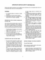
AC
VOLTtoETER
TEST PROBE
TO EXPOSED
~AL
PARTS
TO KNlWEN
EARTH GROUNl
Figure 1. Leakage Current Test Circuit
SAFETY NOTICE
Many electrical and mechanical parts in this chassis
have special characteristics often pass unnoticed and
the protection afforded by them can not necessarily
be obtained by using replacement components rated
for higher voltage,wattage,etc.
Replacement parts that have these Special safety
characteristics are identified in this manual.and its
supplement electrical components having such features are identified by a ! in the Parts List and
Schematic Diagrams.
Before replacing any of these components. read the
Parts List in this manual carefully. The use of substitute replacement parts that do not have the same
safety characteristics as specified in the Parts List
may create shock. fire. or other hazards.
4
THEORY OF OPERATION
GENERAL
1-3. Horizontal output stage 0305
0305 is a horizontal output switch which is closed
during the scan period and opened during the
flyback. It sinks a driver signal from IC302 through
0304. The flyback period is determined by the
resonance of C316 and deflection yoke. C316
makes the necessary S-correction.
Because of the losses in the deflection yoke, a
linearity correction is required. This is achieved by
L302.
The horizontal screen size can be varied by adjusting L303. The high voltage of 12.5KV for CRT
anode is also generated in the flyback transformer
by use of the flyback pulse.
This is a high-resolution monochrome display monitor,
using a paper-white phosphored CRT with etched
faceplate.
It uses one video signal input and separated sync
signals.
It can operate in all of the VGA modes.
DESCRIPTION
1. Main Board
1-1. Power Supply
This is a constant-frequency switch-mode power
supply using L4960 monolithic integrated circuit.
The output voltage regulation is achieved by means
of a variable duty cycle. The output voltage of this
power supply is fed back into tbe pin 2 of L4960.
This voltage is compared to reference voltage internally. The difference of these voltages control
the duty cycle of output current. 0401 to 0404,
and C404 to C405 from input DC supplier.
C408, C409, R404 are the components for frequency compensation, R403, C406 are for oscillation of sawtooth wave. C407 is for soft start of this
circuit. 0405 is a flywheel diode for continuous
flowing current. Output voltage is varied byadjusting VR401 potentiometer.
1-4. Vertical processor IC 201
IC201 performs following functions.
- Vertical oscillator
- Ramp generator
- Linearity control
- Output amplifier
There are three vertical size controls : VR202,
VR203, and VR204. VR202 is for mode 3, VR203
for mode 2, and VR204 for mode 1. Each mode
is automatically selected by IC301.
1-5. Dynamic Focus
0501 is used to provide dynamic focus voltage
which is added to G4 voltage of the CRT. This
voltage is needed to change G4 voltage according
to the angle of the beam.
1-2. Horizontal processor IC302
IC302 performs following functions.
- Horizontal oscillator
- Phase-locked loop for frequency and phase
comparison.
- Phase-locked loop to compensate various delay
times of the horizontal output transistor.
2. CRT Board
IC101 (M51392P) contains wide bandwidth video
amplifier, gain control, pedestal clamp and brightness control circuit.0103 and 0104 from a cascade
video amplifier circuit of which its output is applied
to the cathode pin of the CRT.
The sync signal from 0303 is fed into pin 3 of
IC302 and flyback pulse into pin 4. These two
signals are compared and the circuit is locked to
a correct frequency and phase.
5
3. Line Filter Board
This board contains fuse and EMI filter components.
IMPORTANT:
When replacing the power supply, make sure that
the black ground wire is properly attached to the
main chassis frame. When replacing the fuse,
make sure that the fuse is of the same type and
rating as the original.
*NOTE:
The adjustment requires the connection of a personal computer to the monitor. Although the
monitor is adjusted before it is delivered, readjustment may be required when the setting position
is changed or when a component is replaced.
6
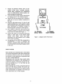
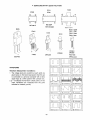
MAJOR OPERATING COMPONENTS
Ml2671
1. FRONT VIEW
t;;;;;;;;;;;;;;;;;~~~~--POWER SWITCH
--POWER INDICATOR
1) Power Switch
: Push the power switch to tum the unit ON.
2. REAR VIEW
2)
3)
4)
5)
6)
Power Indicator
Brightness Control
Contrast Control
Signal cable
Power Cord
:
:
:
:
:
When. the monitor Is on, the power Indicator(Green) wUI light go on.
Turning this control adjusts the overall brightness.
Turning this control adjusts this display contrast.
Connector to the terminal of CPU.
.
Connect with specified outlet
7
MAJOR OPERATING COMPONENTS
ML4671
1. FRONT VIEW
r---- POWER
~
~~;§§§§~~~----POWER
1) Power Switch
SWITCH
INDICATOR
: Push the power switch to turn the unit ON.
2. REAR VIEW
BRIGHTNESS
10
CONTRAST--
•
0 01
I
~~~~---SIGNAL CABLE
-======<f===
2)
3)
4)
5)
6)
Power Indicator
Brightness Control
Contrast Control
Signal Cable
Power Cord
:
:
:
:
:
-POWER CORD
When the monitor is on, the power indicator(Green) will light go on.
Turning this control adjusts the overall brightness.
Turning this control adjusts this display contrast.
Connector to the terminal of CPU.
Connect with specified outlet
8
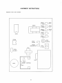
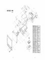
DISASSEMBLY INSTRUCTIONS
1. Fig. A (CABINET)
Loosen two screws (A) holding Cover·Rear and Cover·
Front, and the screw (B) in order to release the Cover·
Rear from the Chassis·Frame, and the screw (C) in order
to release Cover· Rear from the Back-Holder, Cord.
Remove the Cover-Rear by pulling Cover-Rear backward
while pushing the inner latches in direction of (E), using
two jigs(D).
2. Fig. B (PWB's)
1) The CRT must be discharged firstly. Refer to the high
voltage discharge procedure for important safety precau·
tions.
2) Remove the CRT's anode cap(a) from the CRT.
3) Disconnect the ground lead and remove the PWB-CRT
from the Chassis-Frame.
4) Remove Chassis· Frame from the Cover-Front by loosening screws (b).
5) Loosen two screws (c) holding the Chassis-frame and
Back-Holder, Cord.
6) Loosen five screws (d) from the Chassis-Frame and
remove PWB·Main.
7) loosen two screws (e) from the Chassis-Frame and remove
PWB·Power.
8) Loosen four screws (f) to remove Trans·Power from the
Chassis·Frame.
9) Remove the lug·terminal from the Chassis· Frame by
unscrewing (g).
FIGURE B. PCBS
1
j;EfJJ
~ /lj~L
I
(MATERIAL STEEL PLATE)
FIG 2
~v
1
FIG 1
9
VIDEO
0-SIGNAL
VIDEO
INTER FACE
I C 1 0 \
n
VIDEO
VIDEO
DRIV E
0101,0102
OUTPUT
0103 0104
/
I
I
I
I
I
I
I
I
I
I
I I
CRT
14"(12")
t
oY
SYNC.
VERT. O~--t104 INTERFACE
SYNC .......
I C 301
CRT
I C
CONTROL
CIRCUIT
VE R T.
DRIVE
r-......
----
BRIGHTNESS
VR502
CONTRAST
VR 102
8
OUTPUT
2 0 I
0501
---...
L20l,L301
o
F B T
HORZ. O~------~
SYNC .......
HORZ. DRIVE
HORZ.
0303,0304
OUTPUT
I C302, T301
0305
~
T302
POWER
NOISE
AC POWFR
R EGULATO R
FILTER
I--~..t TRANSFOR- ~---....
INPUT ·OD----t~
C401,C402
I C 401
MER
C403
T401
B+
-........,:r-
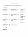
ADJUSTMENT METHOD
SEQUENCE
ITEM
ADJUSTED BY
GOAL
ADJ. CONDITION
1
B+(FBT SUP- VR401
PLY VOLTAGE) (V-ADJST)
+24± 0.2V
2
H -HOLD
VR301
(H-HOLD)
Adjust screen at
horizontal center
position of raster.
3
H-L1NEARITY
L302
(H-L1N)
A same character
size of horizontal
axis.
FULL CROSS
HATCH PATTERN or
FULL "H"PATTERN.
4
H-WIDTH
L303
Refer to the page 4.
~MODE3)
et FULL WHITE
PATTERN and
bringhtness 30F/L.
Next, change to CROSS
HATCH PATTERN
S
V-HOLD
VR201
Vertical free running Frequency:
S4±2(Hz).
No signal.
6
V-LINEARITY
VR20S
A same character
size of Vertical
axis
FULL CROSS-HATCH
PATTERN or FULL
"H" PATTERN
7
V-SIZE
1)VR202
(V-SIZE1)
2)VR203
(V-SIZE2)
3)VR204
(V-SIZE3)
Refer to the page 4.
(MODE3)
A same sequence
7-1. (MODE2)
A same sequence
7-1.(MODE1)
A same condition
as the adjustment
method sequence #4.
8
CENTERING
CENTERING MAGNET Adjust screen at
OF DEFLECTION
central point.
YOKE
9
TILT
DEFLECTION YOKE
Turn the DY in order
to adjust within
± 1 deg of tilt.
10
GEOMETRIC
G/D COMPENSATION MAGNET
Adjust G/D by magnet in order to
enter within overlay
jig.
11
BRIGHTNESS
VR503
(SUB-BRT.)
Adjust VR503 in
order to instantly
disappear the
back-raster.
Center = position
(detent) of VRS02
(EXT-BRT.)
12
CONTRAST
VR101
(SUB-CONT.)
Adjust VR101 in
order to make
brightness to
40±SF/L.
Set FULL WHITE
PATTERN(MODE3).
Next,set VR102
(CONTRAST) to max.
13
FOCUS
VR501
Ad ust VRS01 in
(F CUS)
6
11
FULL "H" PATTERN
order to make the
total focus of the
screen to optimal
status.
REMARKS
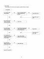
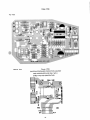
ALIGNMENT INSTRUCTIONS
Alignment Parts and Locations
VR204
V-SIZE
IC201
I
I
I
I
VR205
V-LIN.
VR201
V-HOLD
IC302
o
VR501
FOCUS
C]
VR503 C]
SUB-BRIGHT
O
T301
VR301
H-HOLD
[J
Q305
VR401
(OC24V CONTROL)
IC401
12
MODE
D
M02DE
VR203
V-SIZE
VR202
V-SIZE
IC301
D
D
D
D
@
I
MODE
L303
H-WIDTH
WO
L302
H-LIN·D
3
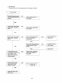
TROUBLE SHOOTING
1. NO POWER
No raster appears and power indicator is not ON in spite of supplying rated AC power input.
NO POWER
Does 32VAC appear between the secondary
leads ofT401?
NO
YES
Does 24V appear between
J401 and ground?
NO
I
NO
NO
Does 9.3V appear between
the #6pin of IC302 and
ground?
YES
NO
Check Q304,R329,T301
YES
Check Q305,D303,
C315,T302.
13
CheckT401.
Check 0401
C404,C405
I
~ 4,
Check 1C401, 0405,
L401, C411, C412,
C413, C420
YES
YES
Does drive pulse appear
at the base of T305?
Does 38V appear between
the #1 pin of 1C401 and
ground?
Check power cord
SW401, F401, C401
C402, C403.
NO
YES
YES
Does the output pulse of
IC302 appear at the #1
pin of 1C302?
Does line voltage appear
between the primary leads
ofT401?
NO
Check R324, R325,
C303,C304
Check 1C302.
2. NO RASTER
Power supply and horizontal circuits operate normally, but there is no raster.
NO RASTER
Is the heater of CRT
bright reddish?
NO
Does 12V appear between
the #4 pin of CRT and
ground?
YES
NO
Check R509, 0503
Check CRT socket,
CRT.
YES
I
•
i Does 12.5KV appear
between the anode
of CRT and ground?
NO
I
CheckT302
I
YES
Does 600V appear
between the #6 pin
of CRT and ground?
NO
YES
Is the voltage of G1
changed by the position
of brightness controls
(VR502,VR503) ?
NO
Does 650Vp-p flyback pulse
appear between the #9 pin
of T302 and ground?
I
Check 8503, C511
R511,D501.
YES
NO
Check VR502,VR503,
Brightness connector assy.
YES
Does 60V appear
between the cathode
of 0502 and ground?
NO
I
Check D502,T302
YES
Check CRT socket,CRT
14
CheckT302.
I
I
3. NO PICTURE
No picture on screen video signal sou'tce is properly connected.
NO PICTURE
Does 60V appear between
the cathode of 0502 and
ground?
NO
Check 0502,T302,C111,
C112,C516
.... ,.
YES
Does proper video signal
appear at the #1 pin of
IC101?
NO
Check signal cable,VR101,
C101,C102.
YES
Does proper video signal
appear at the #8 pin of
IC101?
NO
Does 12V appear between
the #14 pin of IC101
and ground
Does 4.5Vp-p flyback pulse
appear at the #12 pin of
IC101?
YES
Is the waveform at the
to cathode of 0102 similar
the waveform at the
#8 pin of IC101 except
blanking-pulses?
NO
I
Check 0101,0103,0104,
0201,0101,0102,R111,
R116,R117
YES
Does the proper video
signal appear at the
collector of 01 04?
Check R125, 0104
C103, C104
NO
Check R313, R314,
IC101,0302.
I
YES
YES
NO
NO
Check 0104,R120,R122,
R123,R130.
YES
Check R121,S501,CRT,
CRT socket.
15
Check IC101.
4. IMPROPER HORIZONTAL OR VERTICAL SYNCHRONIZATION
There is no stable. It moves horizontal or vertical direction.
[
IMPROPER SYNC.
Do proper horz.and vert.
sync. signals appear at
the end of signal cable?
NO
I Check signal cable.
I
YES
NO
Does picture moves horz.
direction?
YES
YES
Does proper horz.sync.
signal appear at the #3
pin of IC302?
Does proper vert. sync.
signal appear at the #3 pin
of IC301?
NO
I
NO
Check IC301, D530,
R530, C530, C531
Check IC201, C202,
C203, VR201, R206
Check IC301 ,0303,R303,
R304, R305, C302, D530,
R530,C530,C531.
YES
Check IC302,VR301 ,R322,
C305, C306,C311,C312.
5. BLANKING FUNCTION DEFECT.
Vertical retrace line appears on the screen when the external brightness control(VR502) is set to the high
range.
BLANKING FUNCTION
DEFECT
I
Does 5V appear between
the cathode of D530 and
ground?
NO
Check R530,D530,C530,
C531.
I
Check 0201 ,R225,R226,
R227,C215.
16
p.e.BOARD VIEWS
Main PCB
Top View
17
Video PCB
Top View
Bottom View
Power PCB
CAUTION:CONTINUED PROTECTION AGAINST
FIRE HAZARD,REPLACE ONLY WITH
SAME TYPE AND SAME RATING.
18
WIRING DIAGRAM
BLACK
ML2671
___---------~CrRT
VR502QF
WHITE
BLUE (SHIELD)
YELLOW
VRI020F
VR502
VRI02
WHITE
BLACK
FILTER-PCB
.EUROPE
BLACK
WHITE
WHITE (BRN)
VERSION.~~~~~~~~~~~~~~§@~Af~~~~~~1
•
BLACK
WHITE
'BLACK (COAX/ALI
BLACK(SHIELD GND)
WHITE (BLU)
m
==
SIGNAL CABLE
POWER CORD
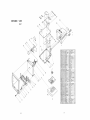
EXPLODED VIEW
ML2671
4St 4543- 704-210
.,
8
3~-402-040
SPTE T0306
ML 4671A
POWER-CORD ..... C. ASSY MD 1.256A
46 8033- 725-940
LABEL-RATING
45 6000-709-010
COVER-BACK
: :YVESTER TO.I
Ml267 I
o BGE MO-1267
44 7148-530-122
SCREW-TAP. RH
2S-3X 12 FE FZY
43 7008- I 40-253
SCREW-PH
M4X25 FE rZB
426601-703-010
HOLOER-CORO{L)
NORYL PX- I 005 VO BGE 00
41 M904-00Q-4030
ASSY-TRANS
Ml 4671 ....
40 M904-00Q-4050
39 7028- 140-08 I
ASSy-PCe POWER AC
SCREW-TH
•
+M4X8 FE FZY
38 7154-230-081
37 7148-530- eel
SCREW-TAP PH
2S-3X8 FE FZY W/WASHER
SCREW- TAP. RH
2S-3X 8
36 5682-702-710
HEATSINK-IC
AI0505 HI4 T2.0 WHT
357048-130-121
34 7304-701-110
SCREW-RH
+3MX12 FE FZY
WASHER-REC
SBC-I TI.5 NI
33 2159-401-020
TRANSISTOR
000033
FE FZY
PLATE-MICA
3M PC(22X28.5)
31 4542-707-110
SHIELD-FBT
SBC- I SN ML4671
30 7318- 103-001
WASHER-SPRING
pI 3.0
29 3934-103-110
INSULA TOR- TR
4.5-80 2-2H N66
28 7208-1 13-001
NUT-HEX
I-M3 FE FZY
27 71 48-!530-081
SCREW-TAP ,RH
2S-3X8 FE FZY
262119-601-900
IC-POWER
L 4960 (SGS)
25 7154-230-081
SCR£W- T AP, PH
FE FZY
v-a
2S-3X8 FE FZY W/WASHER
24 M904-000-4000
ASSY-PCB, MAIN
ML 4671A
23 5684-701-710
HEATSINK-IC 1170
SBC-I TI.O SN
22 7048- I 40-081
SCREW-RH
M4X8 FE FZY
21,7328-204-001
WASHER-TOOTHED
B PI6XPUX T0.5 FE FZY
2~
6,021 -702-5 I 0
CHASSIS-FRAME
SECC TO.8
!,~
,¥905- 000-27
ASSY -CONTRAST, VR
MD .... 1267
ASSY-BRIGHT, VR
MO-1267
I~ 3029- 702 -210
SWITCH-PUSH
ES88213V
16 '7048-130-031
15 7622-701-510
SCR£W-RH
+M3X8 FE FZY
14
M904-000-4020 KNOB- VR
13
7154,- 230-0
ASSY-PCB CRT
4042-706-110
SCREW-TAP, PH
HEATSINK - VIDE-O
12
II
10
9
8
7
6
5684-706-318~
6460-700-210 SHIELD -VIDEO
M9Q4-0Q0-3260 SUPPORT- CHASSIS
~~4- 701-010
2019-125-410
7128-540- 2
19~1
I
ML 4671A
323914-700-410
8, ,M90!5- 000-27
4
SHEll)- 8. V IDEO
CABLE -SIGNAL. ASSY
473053-815-210
PPO VO BGE
2
ML4671A.
2S-3X8FE FZY
A1050$ H14 TID WHW:SI-£R
ST-PE
T0.306
NOYRL PX 1005 PPO VO BG E
ML 2571A
ASSY OY
EARTH-PLATE
CRT -MONOCHROME
5
7304-101-
SCREW-TAP. TH
4
6000-708-010
WASHER-PLAIN
2
M905-000-2600
SPRING-COIL
PBS3 SP-H TO,3
12HBYWDN
2S - 4X20FE FZY
4
165216 FE FZY
4
PPO VO BGE OOOZZZZBC
I 7622-701-810
NO
CODE NO.
20
ASSY-LED
KNOB-POWER
DESCRIPTION.
21
SUS-302 WPA PIO. 5
ML 4671A
PPO VO BGE MO- I 267
SPECIFICATION
'TV
41
EXPLODED
VIEW
ML4671.
3
16
49 3914-700-410
PLATE - MlCA
467048-140-081
SCREW-RH
41 7328 -204-001
WASHER- TOOHEO
B PI6X PI4XTQ5 FE FZY
2
WASHER-PLAIN
165216 FE FZY
25-4040
4
4
7304-101-190
PC
(22)(8.5)
M4Xe FE
FZY
45 3054-81 1-810
POWER-CORD
44 3053-402-0 I 0
25-4040
43 61 14- 144-21 0
SIGNAL-CABLE
LABEL-SERIAL
42 6000-707-510
COVER-REAR
NORYL PX I 005 VO BGE
41 5682-702-710
WHITE PAPER 120
HEATSINK-IC
AI050S HI4 T2.0 WHT
40 2149-202-330
TRANSISTOR
39 7048- 130- J 21
SCREW-RH
000033
+M3X12 FE FZY
38 7304-701-\ 10
WASHER-REC
S8C-1 TI.5 NI
37 4542-705-321
36 7326- r03-Q(H
SHIELD-FBT
SBC-I SN
WASHER-SPRING
PI 3.0 FE
353934-103-110
INSULATOR-TR
2-2H N66 VO
34 7208- I I 3-00 I
NUT -HEX
FZ~
I-M3 FE FZY
M4X2~ FE FZB
2S-4X15 FE FZY
Ml 4671 A
ML 4671A
33 700B-140-253
SCREW-PH
32 7126-540-150
SCREW-TAP. TH
31 M904-000-4030
30 M904-000-40!50
ASSY-TRANS
ASSY-PCB POWER,AC
29 7028- 140-081
SCREW-TH
+M4X8 FE FZY
28 7154-230-081
SCREW- TAP, PH
2S-3X8 FE FZY W/WASHER
27 7148-530-081
SCREW- TAP, RH
2S-3X8 FE FZY
26 7148-530-081
SCREW-TAP,RH
2!5 21 19-60 1-900
24 7154-230-081
IC-POWER
SCREW-TAP ,PH
2S-3X8 FE FZY
L4960(SGSJ
I
I
2S-3X8 FE FZY W/WASHER
5
23 M904-000-4000
ASSy-pee,MAIN
225684-701-710
HEATSINK-IC 1170
ML 4671A
SBC-I TI.O SN
21 6601-703-010
HOLDER-CORD
NORYL PX I 005 VO BGE
20 6021-702- 510
19 M904'OQO-4020
CHASSIS
FRAME
ASSY-PCB CRT
'SECC TO.a
ML 4671A
2S-3X8 FE FZY WjWASHER
18 7148-530-081
SCREW-TAP ,PH
17 5684-706- 110
HEATSINK-VIDEO
AI050S HI4 TI.O WHT
16 4542-706-110
SHIELD-VIDEO
SPTE TO.306
1IS M904-000-3260
ASSY DY
14 4554-701-010
13 64-702-210
EARTH-PLATE
WASHER-RUBBER
ML 2571A
PBS3 SP-H TO.3
C,R BlK
12 7128-540-201
SCREW-TAP,TH
2S-4X20 FE FZY
1 1 20 19- 132-6 I 0
I a M9015-000-2580
CRT -MONOCHROME
ASSY-BRIGHT,VR
I 4HBYWDN
Ml 4671 A
9 7622-701-610
KNOB-VR
PPO
8 M905-000-2590
ASSY-CONTRAST.vR
ML 4671 A
7 6460-700- I 10
SUPPORT -CHASSIS
NORYL PX 1005 VO BGE
va
BGE
6
M~05-000-2600
ASSY LEO
ML 467 I A
IS
31529-702-7 I 0
SWITCH-PUSH
SCREW-RH
ESB 8213V
+M3X8 FE FZY
COVER-FRONT
SPRING-COIL
KNOB-POWER
NORYL PX I 005 VO BGE
SUS-302 WPA PIO.5
4 7048-130-081
6000-706-010
6674-713-710
I
NO
22
3M
7622-701-610
COOE
NO.
23
DESCRIPHON
NORYL VO BGE
SPECIFICATION
REPLACEMENT PARTS LIST
PRODUCT SAFETY SHOULD BE CONSIDERED WHEN A COMPONENT REPLACEMENT IS MADE IN ANY
AREA OF THIS UNIT WITH A COMPONENT INDICATED BY A SAFETY-CRITICAL MARK.
THIS PARTS LIST AND THE SCHEMATIC DIAGRAM SHOW COMPONENTS WHOSE VALUE HAVE SPECIAL
SIGNIFICANCE TO PRODUCT SAFETY. IT IS PARTICULARLY RECOMMENDED THAT ONLY PARTS
SPECIFIED ON THE FOLLOWING PARTS LIST BE USED FOR COMPONENT REPLACEMENT POINTED OUT
BY THE SAFETY CRITICAL MARK.
Ref No.
Part No.
Description
ASSY-PWB,MAIN
0509-400-116
WIRE-SO,COPPER;TA 0.6SN
8P
3053-605-31 0
CONN-8P ASSY;ML4671
C201
1416-318-471
C-CERAMIC,HK;CK45 B 50V 470-K
C202
1509-121-260
C-POLYESTER;C0921 M 100V 0.1 M-J
C203
1509-121-750
C-POLYESTER;C0921M 100V 0.15M-J
C204
1417-344-1 04
C-CERAMIC,HK;CK45(T)F50V 0.1 M-Z
C205
1609-401-720
C-ELECTROLYTIC;CE04W 25V 1000M
C206
1609-402-100
C-ELECTROLYTIC;CE04W 35V 100M
C207
1505-724-332
C-POLYESTER;C0921 M(T) 100V 0.0033-K
C208
1517-383-104
C-M,POLYESTER;CF922M 250V 0.1 M-J
C209
1517-383-104
C-POLYESTER;CF922M 250V 0.1 M-J
C210
1608-904-470
C-ELECTROLYTIC;CE04W(T) 25V 47M
C211
1417-318-101
C-CERAMIC,HK;CK45(T) B50V 100-K
C212
1608-905-220
C-ELECTROLYTIC;CE04W(T) 35V 22M
C213
1505-723-1 04
C-POLYESTER;C0921M(T) 100V 0.1M-J
C214
1609-40 1-51 0
C-ELECTROLYTIC;CE04W 16V 1000M
C215
1608-908-068
C-ELECTROLYTIC;CE04W(T) 100V 0.68M
C220
1417-318-221
C-CERAMIC,HK;CK45(T) B50V 220-K
C300
1417-318-101
C-CERAMIC,HK;CK45(T) B50V 100-K
C301
1608-906-047
C-ELECTROLYTIC;CE04W(T) 50V 0.47M
C302
1509-121-070
C-POLYESTER;C0921 M 100V 0.0027M-J
C303
1417-344-104
C-CERAMIC,HK;CK45(T) F50V 0.1 M-Z
C304
1609-402-120
C-ELECTROLYTIC;CE04W 35V 330M
*C305
1509-452-180
C-POLYSYTRENE;C009S 50V 1500-J
24
Remark
Ref No.
Description
Part No.
*C306
1S0S-725-102
C-POLYESTER;CQ921 M(T) 100V 0.001-K
C307
1S0S-724-332
C-POLYESTER;CQ921 M(T) 100V 0.0033-K
C308
1608-906-1 09
C-ELECTROLYTIC;CE04W(T) SOV 1M
C311
1S09-121-260
C-POLYESTER;CQ921 M 100V 0.1 M-J
C312
1S0S-723-1 03
C-POLYESTER;CQ921M(T) 100V 0.01-J
C313
1S09-121-070
C-POLYESTER;CQ921 M 100V 0.0027M-J
*C314
1S09-121-260
C-POLYESTER;CQ921M 100 0.1M-J
*C31S
1S07-SS3-183
C-POLYPROPYLENE;CQ922M 630V 0.018M-J
*C316
1S39-00 1-2S0
C-M,PAPER;CH021 H 2S0V 2.5M-K
*C404
1603-9S 7-222
C-ELECTROLYTIC;CEO~63V 2200UF(22X30)
C40S
1417-344-104
C-CERAMIC,HK;CK4S(T) F SOV 0.1 M-Z
C406
1S0S-723-222
C-POLYESTER;CQ921M(T) 100V 0.0022-J
C407
1417-329-102
C-CERAMIC,HK;CK4S(T) D SOV 1000-M
C408
1417-318-331
C-CERAMIC,HK;CK4S(T) B SOV 330-K
C409
1S05-723-1 03
C-POLYESTER;CQ921M(T) 100V 0.01-J
C411
1603-90S-471
C-ELECTROLYTIC;CE04W 3SV 470M
C412
1603-90S-471
C-ELECTROLYTIC;CE04W 3SV 470M
C413
1417-344-104
C-CERAMIC,HK;CK4S(T) FSOV 0.1 M-Z
C414
1608-904-100
C-ELECTROLYTIC;CE04W(T) 2SV 10M
C420
1603-90S-471
C-ELECTROLYTIC;CE04W 3SV 470M
CS01
1609-402-2S0
C-ELECTROLYTIC;CE04W SOV 10M
CS02
1SOS-723-1 04
C-POLYESTER;CQ921M(T) 100V 0.1M-J
CS03
1S0S-723-562
C-POLYESTER;CQ921M(T) 100V 0.0056M-J
CS04
1S17-353-223
C-M,POLYESTER;CF922M 630V 0.022M-J
CS15
141 9-901 -1 00
C-CERAMIC,HK;CK45B 1KV 0.01 M-K
C516
1609-403-100
C-ELECTROLYTIC;CE04W 100V 100M
CS17
1609-401-700
C-ELECTROLYTIC;CE04W 2SV 330M
CS18
1609-403-180
C-ELECTROLYTIC;CE04W 160V 2.2M
C530
1417-344-104
C-CERAMIC,HK;CK(4S(T) F SOV 0.1 M-Z
C531
1608-903-101
C-ELECTROLYTIC;CE04W (T) 16V 100M
D201
2169-301-410
DIODE; 1N4148
D202
2169-301-410
DIODE;1N4148
I
25
Remark
Ref No.
Part No.
Description
D203
2169-206-100
DIODE;RGP10G
D301
2169-301-410
DIODE;1N4148
D302
2169-403-697
DIODE-ZENER;RD 6.8EB1 (T)
*D303
2169-206-190
DIODE;RGP30G
D304
2169-206-100
DIODE;RGP10G
*D401
2169-201-240
DIODE;1 N5402(200V 3A)
*D402
2169-201-240
DIODE;1 N5402(200V 3A)
*D403
2169-201-240
DIODE;1 N5402(200V 3A)
*D404
2169-201-240
DIODE;1 N5402(200V 3A)
D405
2169-219-330
DIODE;RG2Y/BYW 100-100
D501
2169-206-020
DIODE;RGP 01-12 RGP02-12
D502
2169-206-170
DIODE;RGP 15J
D503
2169-206-170
DIODE;RGP 15J
D504
2169-206-100
DIODE;RGP 10G
D530
2169-403-557
DIODE-ZENER;RD 5.1 EB1 (T)
EX-BRT
3344-153-010
CONNECTOR-PIN,BASE;B2B-XH-A(JST)
G1G2G4
3054-614-910
CONNECTOR-3P ASSY;JST HOUS 3P-SVF(300MM)
H+IC
7108-530-061
SCREW-TAP PH;2S-3x6 FE FZV
H-DY
3344-112-010
CONNECTOR-WAFER;5273-o2A MOLEX
HN
3344-153-040
CONNECTOR-PIN,BASE;B5B XH-A(JST)
*IC201
2119-101-270
IC;TDA1170N KA2136
*IC301
2109-104-700
IC;KS74HCTLS86N
*IC302
2119-103-130
IC;MC1391P
*IC401
2119-601-900
IC-POWER;L4960
IC401
5682-702-710
HEATSINK-IC;A1050S H14 T2.0 WHT
*L302
2449-733-210
COIL-H,LlNEARITY;5.0-18.3UH
*L303
2449-433-310
COIL-H,WIDTH;7.0-29.9UH
*L401
2429-060-110
COIL-CHOKE;200UH
LED
3344-153-01 0
CONNECTOR-PIN,BASE;B2B-XH-A(JST)
PCB
3006-300-31 0
PCB-MAl N (ML4671); 197x153x1.6T
0201
2139-301-070
TRANSISTOR;2N3904
0301
2139-301-070
TRANSISTOR;2N3904
0302
2139-301-070
TRANSISTOR;2N3904
-
26
Remark
Ref No.
Part No.
Description
0303
2139-301-070
TRANSISTOR;2N3904
*0304
2149-301-437
TRANSISTOR;KSC1008-Y(T)
*0305
2149-304-120
TRANSISTOR;SGS F461
0305
3914-700-410
PLATE MICA;3M PC(22x28.50)
3934~103-110
INSULATOR-TR;4.5-8D 2-2H N66 CoO
0305
4542-707-110
SHIELD-FBT;SBC-1 SN ML4671
T302
2859-129-010
TRANS-FBT;FMG-1235EL
*0501
2139-204-070
TRANSISROR;MPS A45
R200
1018-277-331
R-CARBON;RD 1/4T 330-J
R201
1018-277-273
R-CARBON;RD 1/4T 27K.:~
R202
1018-277-331
R-CARBON;RD 1/4T 330-J
R203
1018-277-274
R-CARBON;RD 1/4T 270K-J
R204
1018-277-103
R-CARBON;TD 1/4T 10K-J
R205
1018-377-100
R-CARBON;RD 1/2T 10-J
R206
1018-277-563
R-CARBON;RD 1/4T 56K-J
R207
1018-277-304
R-CARBON;RD 1/4T 270K-J
R208
1018-277-274
R-CARBON;RD 1/4T 270K-J
R209
1018-277-125
R-CARBON;RD 1/4T 1.2M-J
R210
1018-277-563
R-CARBON;RD 1/4T 56K-J
R215
1018-277-823
R-CARBON;RD 1/4T 82K-J
R216
1018-277-272
R-CARBON;RD 1/4T 2.7K-J
R217
1018-277-273
R-CARBON;RD 1/4T 27K-J
R218
1018-277-473
R-CARBON;RD 1/4T 47K-J
R219
1018-277-339
R-CARBON;RD 1/4T 3.3-J
R220
1018-277-123
R-CARBON;RD 1/4T 12K-J
R221
1018-377-109
R-METAL,FILM;RM 1/2T 1-J
R225
1018-277"222
R-CARBON;TD 1/4T 2.2K-J
R226
2028-377-182
R-CARBON;TD 1/4T 1.8K-J
R227
1018-277-100
R-CARBON;RD 1/4T 10-J
1018-277-683
R-CARBON;RD 1/4T 68K-J
R300
1018-277-331
R-CARBON;RD 1/4T 330-J
R301
1018-277-273
R-CARBON;RD 1/4T 27K-J
0305
~.
R240
-
Remark
"
-"
27
Ref No.
Part No.
Description
-
.
R302
1018-277-331
R-CARBON;TD 1/4T 330-J
R303
1018-277-103
R-CARBON;RD 1/4T 10K-J
R304
1018-277-222
R-CARBON;RD 1/4T 2.2K-J
R305
1018-277-273
R-CARBON;RD 1/4T 27K-J
R310
1018-277-272
R-CARBON;RD 1/4T 2.7K-J
R312
1018-277-472
R-CARBON;TD 1/4T 4.7K-J
R313
1018-277-472
R-CARBON;TD 1/4T 4.7K-J
R314
1018-277-102
R-CARBON;TD 1/4T 1K-J
R320
1018-277-182
R-CARBON;RD 1/4T 1.8K-J
R321
1018-277-102
R-CARBON;RD 1/4T 1K-J
R322
1018-277-153
R-CARBON;RD 1/4T 15K-J
R323
1018-277-104
R-CARBON;TD 1/4T 100K-J
R324
1018-377-331
R-CARBON;RD 1/2T 330-J
R325
1018-277-331
R-CARBON;RD 1/2T 330-J
R326
1018-277-123
R-CARBON;RD 1/4T 12K-J
R327
1018-277-332
R-CARBON;RD 1/4T 3.3K-J
*R328
1018-277-103
R-CARBON;RD 1/4T 10K-J
*R329
1016-377-829
R-CARBON;RD 1/2T 8.2-J
R330
1018-277-101
R-CARBON;RD 1/4T 100-J
R331
1018-277-471
R-CARBON;RD 1/4T 470-J
R355
1045-527-391
R-METAL,OXIDE;RS2P 390-J
R403
1018-277-152
R-CARBON;RD 1/4T 1.5K-J
R404
1018-277':153
R-CARBON;RD 1/4T 15K-J
*R405
1018-277-392
R-CARBON;RD 1/4T 3.9K-J
*R406
1018-277-122
R-CARBON;RD 1/4T 1.2K-J
R410
1018-277-331
R-CARBON;RD 1/4T 330-J
R411
1018-277-102
R-CARBON;RD 1/4T 1K-J
R502
1018-277-103
R-CARBON;RD 1/4T 10K-J
R503
1018-277-472
R-CARBON;RD 1/4T 4.7K-J
R504
10 i 8-277-685
R-CARBON;RD 1/4T 6.8M-J
R505
1018-277-124
R-CARBON;RD 1/4T 120K-J
R506
1018-277-334
R-CARBON;RD 1/4T 330K-J
28
Remark
Ref No.
Part No.
Remark
Description
R507
1018-277-182
R-CARBON;RD 1/4T 1.8K-J
R515
1018-277-125
R-CARBON;RD 1/4T 1.2M-J
R516
1018-277-225
R-CARBON;RD 1/4T 2.2M-J
R520
1018-277-823
R-CARBON;RD 1/4T 82K-J
R521
1018-277-103
R-CARBON;RD 1/4T 10K-J
R530
1049-427-221
R-METAL,OXIDE;RS1P 220-J
*T301
2849-031-611
TRANS-H,DRIVE; 19x7.6MM
TR
7304-701-110
WASHER REC;SBC-l T1.5NI
TR
7208-113-001
NUT-HEX;l M3 FE FZV
TR
7048-130-121
SCREW-RH; + M3Z12FE PZY
TR
7304-700-920
WASHER-PLAIN;9S4810 FE PZW
V-DY
3344-127-710
CONNECTOR-PIN,BASE;JST RTB-1.5-2F
VR201
1241-110-010
VR-SEMI;CET 117A Bl00K
VR202
1241-110-014
VR-SEMI;CET 117A B200K
VR203
1241-110-006
VR-SEMI;CET 117A B500K
VR204
1241-110-006
VR-SEMI;CET 117A BSOOK
VR20S
1241-110-00S
VR-SEMI;CET 117A BSOK
*VR301
1241-108-003
VR-SEMI;CET 92A B5K
*VR401
1241-108-011
VR-SEMI;CET 92A B1K
VRSOl
1241-108-012
VR-SEMI;CET 92A B2.SM
VR503
1241-108-010
VR-SEMI;CET 92A B2S0K
PCB CRT/FILTER
0509-400-116
WIRE-SO,COPPER;TA 0.6 SN
Cl01
lS09-121-260
C-POLYESTER;CQ921M 100V O.OlM-J
Cl0Z
1609-401-680
C-ELECTROLYTIC;CE04W 25V 10M
Cl03
1609-401-480
C-ELECTROLYTIC;CE04W 16V 220M
Cl04
1419-204-820
C-CERAMIC,HK;CK45 F SOV 0.1 M-Z
Cl0S
1419-204-820
C-CERAMIC,HK;CK45 F SOV 0.1 M-Z
Cl06
1609-402-230
C-ELECTROLYTIC;CE04W 50V 3.3M
Cl07
1419-109-140
C-CERAMIC,HK;CK4S B 50V 0.01 M-Z
Cl08
1417-318-101
C-CERAMIC,HK;CK4S(f) B 50V 100-K
Clll
1609-403-090
C-ELECTROLYTIC;CE04W 100V 47M
29
,
Ref No.
Part No;
Description
Cl12
1419-204-820
C-CERAMIC,HK;CK45 F 50V 0.1 M-Z
C510
1419-106-250
C-CERAMIC,HK;CK45 B 500V 0.01 M-K
C511
1419-901-100
C-CERAMIC,HK;CK45 B 1KV 0.01 M-K
CONTRAST
3344-153-010
CONNECTOR-PIN,BASE;B2B-XH-A(JST)
0101
2169-301-410
DIODE; 1N4148
0102
2169-301-410
DIODE;lN4148
0104
2169-406-020
DIODE-ZENER;l N4741A(11V)
G1G2G4
3344-120-810
PIN-BASE;JST RTB-l.5-3 VO WHT
H+V
7108-530-061
SCREW-TAP PH;2S-3x6 FE FZY
*IC101
2109-104-610
IC;M51392P
IN-SIGNAL
3344-120-060
CONNECTOR-PIN,BASE;B8B-XH-A
PCB
3006-300-340
PCB-CRT(ML4671); 105x67x1.6T
0101
2139-401-750
TRANSISTOR;2N3906(SST)
0102
2139-301-070
TRANSISTOR;2N3904
*0103
2149-301-360
TRANSISTOR;2N2369
0104
4543-704-210
SHIELD-B VIDEO;SPTE TO.306
Q104
5684-706-310
HEAT-SINK,VIDEO;SBC-1 Tl.0 FE FT-2
*0104
2149-302-300
TRANSISTOR;MPS-U06
R101
1018-277-561
R-CARBON;RD 1/4T 560-J
R102
1018-277-121
R-CARBON;RD 1/4T 120-J
Rl03
1018-277-302
R-CARBON;RD 1/4T 3K-J
R104
1018-277-332
R-CARBON;RD 1/4T 3.3K-J
R105
1018-277-222
R-CARBON;RD 1/4T 2.2K-J
R106
1018-277-333
R-CARBON;RD 1/4T 33K-J
R107
1018-277-472
R-CARBON;RD 1/4T 4.7K-J
Rl08
1018-277-222
R-CARBON;RD 1/4T 2.2K-J
R109
1018-277-102
R-CARBON;RD 1/4T 1K-J
R110
1018-277-222
R-CARBON;RD 1/4T 2.2K-J
R111
1018-277-471
R-CARBON;RD 1/4T 470-J
Rl15
1018-277-472
R-CARBON;RD 1/4T 4.7K-J
R116
1018-277-470
R-CARBON;RD 1/4T 47-J
Rl17
1018-277-470
R-CARBON;RD 1/4T 47-J
R118
1018-277-560
R-CARBON;RD 1/4T 56-J
30
Remark
Ref No.
Part No.
Description
Rl19
1018-277-101
R-CARBON;RD 1/4T 100-J
R120
1018-277-102
R-CARBON;RD 1/4T 1K-J
R121
1018-277-820
R-CARBON;RD 1/4T 82-J
R122
1045-527-471
R-METAL,OXIDE;2P 470-J
R123
1045-527-471
R-METAL,OXIDE;2P 470-J
R125
1045-427-680
R-METAL,OXIDE;RS 1P 68-J
R130
1018-277-102
R-CARBON;RD 1/4T 1K-J
R509
1045-427-680
R-METAL,OXIDE;RS 1P 68-J
R510
1018-377-102
R-CARBON;RD 1/2T 1K-J
R511
1018-377-473
R-CARBON;RD 1/2T 47K-J
R512
1018-377-102
R-CARBON;RD 1/2T 1K-J
R501
2029-010-010
LAMP-NEON;DMS 9O-130V DC
S505
2029-010-010
LAMP-NEON;DMS 90-130V DC
S502
4569-001-110
SPARK-GAS;S-23(1 KV)
S503
4569-001-110
SPARK-GAS;S-23(1 KV)
S504
4569-001-110
SPARK-GAS;S-23(1 KV)
SOCKET
3353-700-910
SOCKET-CRT;7PIN
VIDEO
3344-153-020
CONNECTOR-PIN,BASE;B3B-XH-A(JST)
VR101
1241-110-004
VR-SEMI;CET 117A B200
\
I
POWER- PCB
PCB
3006-300-350
PCB-POWER,AC(ML4671) ;62.5x50x1.6T
3344-131-020
ONNECTOR-WAFER;B3P-VH(3P 3.96MM)
R401
1018-377-684
R-CARBON;RD 1/2T 680K-J
C401
1565-523-224
C-M,POLYESTER,AC;CaS 922M 250V O.22M-M
C402
1461-137-806
C-CERAMIC,AC;DE 7100F 222 MVAI
C403
1461-137-806
C-CERAMIC,AC;DE 7100F 222 MVAI
C415
1565-523-473
C-M,POLYESTER,AC;CaS922M 2S0V 0.047M-M
GND
3124-700-810
PIN-GT;14.2MM 2.35PI
F401
3364-700-210
HOLDER-FUSE;FC51 E,20M/M FUSE
F401
4709-088-OS0
FUSE;51S,250V 1A 20MM
F401
4709-060-010
FUSE;T250V 0.5A 20MM SEMCO
L402
2429-646-510
COIL-LlNE,FILTER;6MH(11x16MM)
31
Remark
Ref No.
T401
Part No.
3344-156-320
Description
CONNECTOR-WAFER;B2P-LV,TN
1-
MISCELLANEOUS
CRT-G
3054-224-210
GND-CRT ASSY;ML2671 ,3/16/0.2
CRT-G
3054-224-220
GND-CRT ASSY;ML4671 ,3/16/0.12 T815
VR102
1201-102-902
VR-ROUND;18SN 10SK B5K
CONTRAST
3054-617 -620
CONNECTOR,2P ASSY;JST-2(2.5) L=340
CONTRAST
4049-032-011
FERRITE-CORE;RING 18 ¢
VR502
1201-102-961
BRIT
3051-640-610
CONNECTOR,2P ASSY;JST HOUS XHP-2(2.5)BRT
LED
2309-11 0-090
LED;KLG 208E
LED
0659-422-500
TUBE-HISHI U/C;SUMITUBE F2 DIA 3.2 FD5 BLK
LED
3054-640-810
CONNECTOR,2P ASSY;JST XHP-2,B +
LED
0659-410-021
TUBE-VINYL,u/C;AWGO 300V 105°C C-CLR
LED
0659-410-621
TUBE-VINYL,U/C;AWG6 300V 105°C C-CLR
SW401
3529-702 -21 0
SWITCH-PUSH;ESB8213V
SW401
0659-422-500
TUBE-HISHI U/C;SUMITUBE F2 DIA3.2 FD5 BLK
SW401
3054-648-310
CONN-2P ASSY;H-YHR-3N L-150M/M
SW401
3054-617-040
CONNECTOR-AC,ASSY;REP,ASSY
SW401
0659-410-021
TUBE-VINYL,U/C;AWGO 300V 1OsoC C-CLR
30S4-402-040
CABLE-SIGNAL;ML4671
DY
2439-054-230
DEFL-YOKE;DMK-1294EL(3)
V-DY
3054-613-750
CONNECTOR-DY,ASSY;CONNECTOR V-DY
H-DY
30S4-618-81 0
CONN-HORZ DY ASSY;2x22AWG
CRT
2019-125-410
CRT-MONOCHROME;12ABY WDN (ML2671 ONLY)
CRT
2019-132-610
CRT-MONOCHROME;14HBY WDN(ML4671 ONLy)
T401
T401
2869-298-030
2869-298-040
Q104
3054-223-730
TRANS-POWER,ASSY;P: 11SV,S:30V
TRANS-POWER,ASSY;P:230V,S:30V
(FOR EUROPE VERSION)
LUG-TERMINAL ASSY;AWG 18 BLK L-150
AC
3054-815-210
POWER CORD,AC,ASSY;K01 01 AS213
AC
3054-812-310
POWER CORD,AC ASSY;LP34 HOS WF
VR-ROUND;18SNC1 10SK B50K
(FOR EUROPE VERSION)
GND
3054-302-210
GND-WIRE ASSY;BLK L-1S0MM 101S#18(T)
32
Remark
• SEMICONDUCTOR IDENTIFICATION
[j
CD
IC201
IC101
IC301
IC302
®
®
®
E::::::I
®
0
CD
MC1391P
®
MS1392P
74HCTLS86N
030S
1C401
0104
0103
TDA1170 N
0101 0102
0201 0301
0302 0303
0304 OSOl
~c
~,~
2N3904
2N3906
2N2369
L4960
KSC1008
MPSU06
SGSF461
MPSA44/45
WAVEFORMS
LbQr12JJ
Waveform Measurement Conditions :
1. The voltage level and waveform at each point are
given below on the rated input power when this set
is connected to a personal computer with a video
signal input at a white pattern with contrast max.
2.0---' indicates the waveform check points. (In the
chart, waveforms are measured from the point
indicated to chassis ground.)
®
5 Vp-p IVI
~
[OJ
®
2eV p-p
®
3,2Vp-p IVI
IVI
~
@
@)22VP-P IHI
IVp-p
IHI
lSQOl!]l!J]
l!J]USB[NJ
33
@)38VP-P(HI
®
6,5Vp-pIHI
@
210Vp-pIHI
®
@
2.4Vp-p
I®
40V p-p
23Vp-p
IHI
3410EM
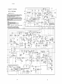
SCHEMATIC DIAGRAM
RI2S@
MODEL NO: ML4671(ML2671)
GND
.~CI03
0104
CHASSIS NO: GSI-1
WAR NI NG: "THIS NONITOR CONTAINS SAFETY
GND
)----<
RECEPTEUR EST EQUIPE OE COMPOSANT CRITIQUES POUR LA
SECURITE TOUTES LES PIECES INDIQUEES DANS LES ZONES OMBREES DU SCHEMA SONT CRITIQUES
POUR LA SECURITE POUR MAINTENIR LE OERGE DE SECURITE DE L' APPA-REIL NE REPLACER LES
COMPOSANTS DONT LEE FONCTIONNEMENT EST CRITIQUE POUR LA SECURITE QUE PAR OES PIECES
RECOMMANDEES PAR LE FABRICANT.
CONSULTER LA NOMENCLATURE DES PIECES POUR TROUVER LES PIECES DE RECHANGE EXACTES.
,-_-...r-R-\4NI"'0_ _ _.,..-_....,..._ _ _+-"""'J~
r·
330
II ~~410
,
G301
2N3904
I
rSt
R310
LY
SA
!~301
,
~~5C2.01
R201
27K
R200
330
I
HS
C20S
tge ou
S
I
rg2~4
R325
R324
330
O.SW
o.SW
330
I
KS74HCTLSBSN
II
I 1300S'VU3
CGPIOG
sl
>AMe
C420
470U
3SV
R302
330
AC
(L)
C300
100
HGT
GND
h
AC I.,J,
@
IV-
SYNC
"I
'1
L402
"
C403
1'2200
I!!9l
SS02
0101
IN414B
~CIII
"47U
100V
SS03
0102
IN414B
RII9
,
SS04
•
+60,
+15
G2 G4
G1
R209
I. 2M
-
G201
~~~O
L.....(>-
220
'.....
R220
12K
.
RSOI
3 3K
~C214
V-LIN
I~IOOOU
__
m~
®
RS04
C504
~~..: ......----_t---ll-+---'--+
S 8M
0.022
G501
S30V
B
~f1°
tv
C501
~S~~
MPSA44/ 45
.n
VRS02
VRS03
~~~~~RT . "--B-SO-K-J
RSIS
I. 2M
EXT-BRT
\"
RS02
10K
~~~-,
RS03
RSOS
RS07
4. 7K
120K
RS20
B2K
VR501
82.SM
RS21
10K
I r---
I. BK
L~~F~O~C~US~______~__________,
1:!:~S~t~
0501
0.01 RGPOI-12
ISV
C209
IO@'IIsCsSo003
@ R221 ® ~gS~2
~.SW
®
R323
I C30S
ISK ::!:r ISOO
::!:r~IOOOP
®
®
I C30S
sl
R32S
II
lOOK
12K
C307
3300
1®
~
7
2
R320
4
R32
d
IK
~:
~03
isC308
R328
10K
f'~U
SOV
R329
8.2
O.SW
1
RGP02-12
IKV
I
I,--I__
~;-~______+-~.~~
R327
C312
3.3K
r
o. OI
®
hIN~4EA
*
W.:::. . . .
@
C401
0.22
2S0V
I
R401
S80K
O.SW
L '"
~~m ~TIOll~T
I
2
'~G304
(N)
S3V
OSC
S
F~tR404
,
ISK
C40B
r330
R403
P
~>--l
0503
0
~h
KSC1008
0303
GP30G
C315
r~IB
B
I ,J,
~~eu
RGPIOG
R405
3.9K
C40S
C414
z~1g~
C ~~~Ol
L-+O-4-0S----+----i'~V-ADJST
C407
I. SKr;O r I O O O ,
RG2Y
i!~~~3 iI~412
3SV
3~eu
Z ~~SI7
OS04 '
I I.cS~8
f"~60~
L401
200UH
~~~8~UI::!:~g4~S ~0L.9.l;i3~-......l1!l4ilL....~-4Si1J'---I-~E..J
:+-
34
GNO
~4rJ~
H-DY
RGPISJ
•
F.a2
CMP
~
R33S
~ao
L3o'1 ....•
OUT~7--~~~--~~-_------4r------~--~-------t-----------------------t~
IC401
L4960
lIN
+I_~.----..."...J
~B
FBT FMG-1235FL
0304
RGPIOG ~)-
',j,.
T~I
~
C311
O.I®
• ~02
C314 ®
- 3- 3-0 "--o-l.~
t-R
100
Mtr~gip
I.BK
G41
RIIB
SS
m8~)- ~~g~ ~2N3904
r-J! ®b=- [ ~~~~
VR301
BSK
H-HOLD
C303
0.1
r
0401-4
n
2W
R227
10
R22S
1.8K
®
RAM
R.G
R322
1
G303
2N3904
1401
I C402
::!:~200
T~sov
r--
®
L402
C41S
0.047
::!:~107 RIIS
1 0 . 01 , 4 7KJ,
r-._-.._--,
Vi
14HBYWDN
0---
G101
2N3906
47
r.
I 10
----""3l
,
2S0V I t
RIIS
I
I
I
C211
R207 6
270K
C208
hOI
R303"'~~pl-2®,...::p"-_R..,,3"'OS---+-----....J
10K • ~ _r
2700
27K
\!::
~:0IF401
71
I
I
I
h
r
47
,.,
I
IC201 -_.
.
R304
2.2K
'-----41-----1-1:
GND
•
o·
I:UMe
2~CC'
R300
GND
,
Cl0S
3.3U
50V
r
I>C304
f"330U
3SV
13
IC301
330
CON RAST
Gil G2
m
G103
2N2369
T302
10
GND
~.
<1
TDA1170N
330
~?o:r
4>--;\ 14
RII7
fmO~I-O"""'-d-.r,----"'R2:-I'::'S-t~R2:-1'::'9-..."'"--,~C21S
470
0, ~
;C212
2.7K
3.3
168~
~2~iI
~
22SU
R217
C213
'-----+
V
I 82K 4
27K
1
__R'IS>A30~_R""2'10'rS_ _ _.,..-_~_ _-<r-_02t>0t-3~r-'C2Bo_s-1
47U
2SV
VS
R301
27K
1
I
:-,~~~g~
,), IN414B
RI09
IK
@ 2W
~W L i - - - o - ,4G
u
k€
~~30
BK
0201
R203
r--+_-f<I-_-'lMr_ _ _ _-\·Nrn+-......,_ _ _L_V~-:.:SIZEI
VR203
IN414B
270K
BSOOK
V-SIZE. 2
0202
R204
R20B C207
270K 13300
IN414B
10K
~~
®
BSOOK
V-SIZE. 3
4.7K
2.2K
CP
i
I
2.7K
~
,
•
SA
H
8r-...JL.--h
9
®
P
,---+--u......,---.,.--------'9!fJSC
0.1 I C203 rliVR201
REF.V
::!:::r!o IS
8100K
.
V-HOLD R20S
®
SSK
R313
4.7K
10
(!7
I
I
I
~S501L-<r~~H\
82
MPSU06
2SV
CP
'CT62
r - - - - - - - . r - - - - R311
470
12111
Q104
RIIO
VG.[J~2~
SU -CONT 0.01
1@22010
IW
o.sw
CS30 .~CS31
• DS30
1 "~tgeu
' ROS.IE81
R411
IK
""LED
3.3Kr.1
~
RI21
G102
2N3904
1
CIOI
I®
~SSOS
470
,-----. RIOB
2.2K
I
IC 10 1
O---h--"'---'~ou r~~U'
I.: "BII'. M51392P
r -_ _
S_A--o_-+,
IS SHOW IN OHM. K-I. 000 M-I. 000. 000.
RATED POWER OF RESISTOR NOT NOTED IN SCHEMATIC DIAGRAM IS 1/4W.
.
2.CAPACITANCE IS SHOWN IN UFo P-UUF (PICO FARAD) .
RATED VOLTAGE OF CONDENSER NOT NOTED IN SCHEMATIC DIAGRAM IS SOV.
3. ABBREVIATION
@ R-METAL FILM
@ R-METAL OXIDE
C-POLYESTER
NON POLAR CAPACITOR
e
~IOS
"
RI06
33K
CI02
RSIOOI RI02 VRIO
S
120 B200
Rill
RI20
IK
1:\31
'"'\
VIDEO
RI07
4.7K
G(
(1)
NOTE
I. RESISTANCE
C-POL YPROPYLENE @ C-METAL
C-POL YESTYRENE
4 .VOL TAGE IS READ WITH SSVM FROM INDICATED POINT TO SIGNAL GROUND.
S. THIS SCHEMATIC DIAGRAM IS SUBJECT TO CHANGE FOR FURTHER IMPROVEMENT.
RI03
3K
~
AVERTIS SMEN T: "CE
®
POLYESTER ®
RI05
2.2K
CI04
1
'~~~eOU
IN4741A
CRITICAL COMPONENTS ALL PARTS SHOWN IN
THE SHADED AREAS OF THE SCHEMATIC ARE SAFETY CRITICAL. FOR CONTINUED SAFETY REPLACE
SAFETY CRITICAL COMPONENTS ONLY WITH MANUFACTURER'S RECOMMENDED PARTS.
REFER TO PARTS LIST FOR EXACT REPLACEMENTS."
*
r·
)--
RS09
S8 IW
~ III
.1
~
f413
R40S
, I. 2K
35
6
0502 '
RGPISJ
I.e!
IIII5~3
100V
CIRCUIT - DIAGRAM
DISPLAY SYMBOLS
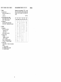
RMS MEASUREMENT RESULTS OF THE IC'S
1. Resistor
Measured with high impedance V.T.V.M. or circuit
tester under the rated line voltage. Volt~ge reading
may vary ± 10%. Video signal is a white pattern and
mode 3.
Unit: Volts
• Resistance value
When no unit is provided : [ Q ]
K : [K- Q ]
M : [M- Q ]
• Rated permissible power capacity
When no display is mode: 1/4[W]
Others : Display are provided
ICS
IC101
IC301
1C302
1C401
74LS86
MC1391P
L4960
2.3
4.8
0.2
38.5
14.5
4.7
0
5.0
1.8
0.4
2.6
2.6
IC201
PIN NO. M51392P TDA1170N
• Resistor type
Under than 1/2[W] : Carbon resistor
Over than 1 [W] : Oxidized metal film resistor
1
2. Capacitor
• Capacitance
When no unit is provided:
1) Electrolytic - LuF]
2) E.T.C - [pF]
Others: Display are provided
• Withstand voltage
No display:
1) Polyester - DC 100[V]
2) E.T.C - DC 50[V]
Others : DC withstand voltage[V]
AC display : AC withstand voltage[V]
2
0
3
2.3
4
6.7
5
0
4.7
2.3
0
0
2.9
2.0
6
3.7
6.5
4.8
9.3
4.8
0
6.8
0
4.1
51.0
8
3.1
0.4
.4.5
3.1
*
*
*
*
*
*
*
*
*
*
*
*
*
9
6.0
2.9
0
10
0
2.0
3.7
11
4.8
0.6
1.3
12
1.4
1.5
3.7
0
*
*
4.2
14
36
7.6
14.0
7
13
• Capacitor type
No type display : Ceramic and electrolytic
capacitor
P : Polyester capacitor
MP : Metallized polyester capacitor
PS : Polystyrene capacitor
3.8
11.8
4.8
Memo
Printed in Korea
Code No.: 8146-400-040