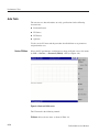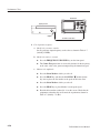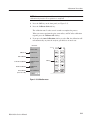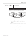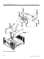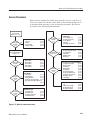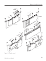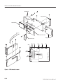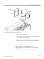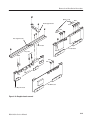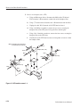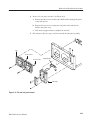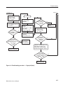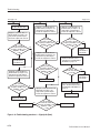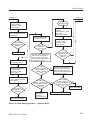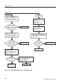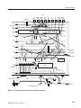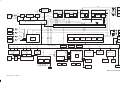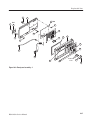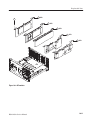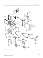
1
Service Manual
RSA3408A
8 GHz Real-Time Spectrum Analyzer
071-1691-00
This document applies to firmware version 3.01
and above.
Warning
The servicing instructions are for use by qualified
personnel only. To avoid personal injury, do not
perform any servicing unless you are qualified to
do so. Refer to all safety summaries prior to
performing service.
www.tektronix.com
Copyright © Tektronix, Inc. All rights reserved. Licensed software products are owned by Tektronix or its suppliers and
are protected by United States copyright laws and international treaty provisions.
Use, duplication, or disclosure by the Government is subject to restrictions as set forth in subparagraph (c)(1)(ii) of the
Rights in Technical Data and Computer Software clause at DFARS 252.227-7013, or subparagraphs (c)(1) and (2) of the
Commercial Computer Software – Restricted Rights clause at FAR 52.227-19, as applicable.
Tektronix products are covered by U.S. and foreign patents, issued and pending. Information in this publication supercedes
that in all previously published material. Specifications and price change privileges reserved.
TEKTRONIX and TEK are registered trademarks of Tektronix, Inc.
Contacting Tektronix
Tektronix, Inc.
14200 SW Karl Braun Drive or P.O. Box 500
Beaverton, OR 97077 USA
For product information, sales, service, and technical support:
H
H
In North America, call 1-800-833-9200.
Worldwide, visit www.tektronix.com to find contacts in your area.
Warranty 2
Tektronix warrants that this product will be free from defects in materials and workmanship for a period of one (1) year
from the date of shipment. If any such product proves defective during this warranty period, Tektronix, at its option, either
will repair the defective product without charge for parts and labor, or will provide a replacement in exchange for the
defective product. Parts, modules and replacement products used by Tektronix for warranty work may be new or
reconditioned to like new performance. All replaced parts, modules and products become the property of Tektronix.
In order to obtain service under this warranty, Customer must notify Tektronix of the defect before the expiration of the
warranty period and make suitable arrangements for the performance of service. Customer shall be responsible for
packaging and shipping the defective product to the service center designated by Tektronix, with shipping charges prepaid.
Tektronix shall pay for the return of the product to Customer if the shipment is to a location within the country in which the
Tektronix service center is located. Customer shall be responsible for paying all shipping charges, duties, taxes, and any
other charges for products returned to any other locations.
This warranty shall not apply to any defect, failure or damage caused by improper use or improper or inadequate
maintenance and care. Tektronix shall not be obligated to furnish service under this warranty a) to repair damage resulting
from attempts by personnel other than Tektronix representatives to install, repair or service the product; b) to repair
damage resulting from improper use or connection to incompatible equipment; c) to repair any damage or malfunction
caused by the use of non-Tektronix supplies; or d) to service a product that has been modified or integrated with other
products when the effect of such modification or integration increases the time or difficulty of servicing the product.
THIS WARRANTY IS GIVEN BY TEKTRONIX WITH RESPECT TO THE PRODUCT IN LIEU OF ANY OTHER
WARRANTIES, EXPRESS OR IMPLIED. TEKTRONIX AND ITS VENDORS DISCLAIM ANY IMPLIED
WARRANTIES OF MERCHANTABILITY OR FITNESS FOR A PARTICULAR PURPOSE. TEKTRONIX’
RESPONSIBILITY TO REPAIR OR REPLACE DEFECTIVE PRODUCTS IS THE SOLE AND EXCLUSIVE REMEDY
PROVIDED TO THE CUSTOMER FOR BREACH OF THIS WARRANTY. TEKTRONIX AND ITS VENDORS WILL
NOT BE LIABLE FOR ANY INDIRECT, SPECIAL, INCIDENTAL, OR CONSEQUENTIAL DAMAGES
IRRESPECTIVE OF WHETHER TEKTRONIX OR THE VENDOR HAS ADVANCE NOTICE OF THE POSSIBILITY
OF SUCH DAMAGES.
Table of Contents
General Safety Summary . . . . . . . . . . . . . . . . . . . . . . . . . . . . . . . . . . . .
Service Safety Summary . . . . . . . . . . . . . . . . . . . . . . . . . . . . . . . . . . . . .
Preface . . . . . . . . . . . . . . . . . . . . . . . . . . . . . . . . . . . . . . . . . . . . . . . . . . .
ix
xi
xiii
Manual Structure . . . . . . . . . . . . . . . . . . . . . . . . . . . . . . . . . . . . . . . . . . . . . . . . .
Manual Conventions . . . . . . . . . . . . . . . . . . . . . . . . . . . . . . . . . . . . . . . . . . . . . .
Related Documentation . . . . . . . . . . . . . . . . . . . . . . . . . . . . . . . . . . . . . . . . . . . .
xiii
xiv
xiv
Introduction . . . . . . . . . . . . . . . . . . . . . . . . . . . . . . . . . . . . . . . . . . . . . . .
xv
Performance Check Interval . . . . . . . . . . . . . . . . . . . . . . . . . . . . . . . . . . . . . . . . .
Strategy for Servicing . . . . . . . . . . . . . . . . . . . . . . . . . . . . . . . . . . . . . . . . . . . . .
xv
xv
Performance Conditions . . . . . . . . . . . . . . . . . . . . . . . . . . . . . . . . . . . . . . . . . . . .
Electrical Characteristics . . . . . . . . . . . . . . . . . . . . . . . . . . . . . . . . . . . . . . . . . . .
Physical Characteristics . . . . . . . . . . . . . . . . . . . . . . . . . . . . . . . . . . . . . . . . . . . .
Environmental Characteristics . . . . . . . . . . . . . . . . . . . . . . . . . . . . . . . . . . . . . . .
Digital IQ Output Connector Pin Assignment (Option 05 Only) . . . . . . . . . . . .
1–1
1–2
1–16
1–16
1–19
RF Input . . . . . . . . . . . . . . . . . . . . . . . . . . . . . . . . . . . . . . . . . . . . . . . . . . . . . . . .
Down Converter . . . . . . . . . . . . . . . . . . . . . . . . . . . . . . . . . . . . . . . . . . . . . . . . . .
Digital Signal Processing . . . . . . . . . . . . . . . . . . . . . . . . . . . . . . . . . . . . . . . . . . .
Power Supply . . . . . . . . . . . . . . . . . . . . . . . . . . . . . . . . . . . . . . . . . . . . . . . . . . . .
External Interface . . . . . . . . . . . . . . . . . . . . . . . . . . . . . . . . . . . . . . . . . . . . . . . . .
3–1
3–1
3–3
3–4
3–5
Specifications
Operating Information
Theory of Operation
Performance Verification
RSA3408A Service Manual
Performance Verification Procedures . . . . . . . . . . . . . . . . . . . . . . . . . .
4–1
Conventions . . . . . . . . . . . . . . . . . . . . . . . . . . . . . . . . . . . . . . . . . . . . . . . . . . . . .
4–2
Brief Procedures . . . . . . . . . . . . . . . . . . . . . . . . . . . . . . . . . . . . . . . . . . .
4–3
Functional Tests . . . . . . . . . . . . . . . . . . . . . . . . . . . . . . . . . . . . . . . . . . . . . . . . . .
Diagnostics . . . . . . . . . . . . . . . . . . . . . . . . . . . . . . . . . . . . . . . . . . . . . . . . . . . . . .
4–4
4–8
Performance Tests . . . . . . . . . . . . . . . . . . . . . . . . . . . . . . . . . . . . . . . . . .
4–9
Prerequisites . . . . . . . . . . . . . . . . . . . . . . . . . . . . . . . . . . . . . . . . . . . . . . . . . . . . .
Equipment Required . . . . . . . . . . . . . . . . . . . . . . . . . . . . . . . . . . . . . . . . . . . . . . .
Auto Tests . . . . . . . . . . . . . . . . . . . . . . . . . . . . . . . . . . . . . . . . . . . . . . . . . . . . . . .
Frequency Checks . . . . . . . . . . . . . . . . . . . . . . . . . . . . . . . . . . . . . . . . . . . . . . . .
Noise Sideband Checks . . . . . . . . . . . . . . . . . . . . . . . . . . . . . . . . . . . . . . . . . . . .
Amplitude Checks . . . . . . . . . . . . . . . . . . . . . . . . . . . . . . . . . . . . . . . . . . . . . . . .
Spurious Response Checks . . . . . . . . . . . . . . . . . . . . . . . . . . . . . . . . . . . . . . . . .
Test Record . . . . . . . . . . . . . . . . . . . . . . . . . . . . . . . . . . . . . . . . . . . . . . . . . . . . . .
4–10
4–10
4–12
4–21
4–25
4–28
4–40
4–52
i
Table of Contents
Adjustment Procedures
Requirements for Performance . . . . . . . . . . . . . . . . . . . . . . . . . . . . . . . . . . . . . .
Equipment Required . . . . . . . . . . . . . . . . . . . . . . . . . . . . . . . . . . . . . . . . . . . . . . .
Preparation . . . . . . . . . . . . . . . . . . . . . . . . . . . . . . . . . . . . . . . . . . . . . . . . . . . . . .
Self Calibration . . . . . . . . . . . . . . . . . . . . . . . . . . . . . . . . . . . . . . . . . . . . . . . . . .
Auto Calibration . . . . . . . . . . . . . . . . . . . . . . . . . . . . . . . . . . . . . . . . . . . . . . . . . .
Reconfiguration of RF Modules . . . . . . . . . . . . . . . . . . . . . . . . . . . . . . . . . . . . . .
5–1
5–2
5–3
5–10
5–14
5–27
Related Maintenance Procedures . . . . . . . . . . . . . . . . . . . . . . . . . . . . . . . . . . . . .
Preparation . . . . . . . . . . . . . . . . . . . . . . . . . . . . . . . . . . . . . . . . . . . . . . . . . . . . . .
Inspection and Cleaning . . . . . . . . . . . . . . . . . . . . . . . . . . . . . . . . . . . . . . . . . . . .
6–1
6–2
6–4
Removal and Installation Procedures . . . . . . . . . . . . . . . . . . . . . . . . . .
6–7
Preparation . . . . . . . . . . . . . . . . . . . . . . . . . . . . . . . . . . . . . . . . . . . . . . . . . . . . . .
Access Procedure . . . . . . . . . . . . . . . . . . . . . . . . . . . . . . . . . . . . . . . . . . . . . . . . .
Procedures for External Modules . . . . . . . . . . . . . . . . . . . . . . . . . . . . . . . . . . . . .
Procedures for RF Modules . . . . . . . . . . . . . . . . . . . . . . . . . . . . . . . . . . . . . . . . .
Procedures for CPU Board and Disk Modules . . . . . . . . . . . . . . . . . . . . . . . . . .
Procedures for Mother Board and Daughter Boards . . . . . . . . . . . . . . . . . . . . . .
Procedures for Power Supply Modules on the Instrument Bottom . . . . . . . . . . .
Procedures for RF1 Modules on the Instrument Bottom . . . . . . . . . . . . . . . . . . .
Procedures for Front Panel Modules . . . . . . . . . . . . . . . . . . . . . . . . . . . . . . . . . .
Procedures for Chassis Modules . . . . . . . . . . . . . . . . . . . . . . . . . . . . . . . . . . . . .
6–7
6–21
6–22
6–27
6–31
6–41
6–46
6–51
6–56
6–62
Troubleshooting . . . . . . . . . . . . . . . . . . . . . . . . . . . . . . . . . . . . . . . . . . . .
6–67
Troubleshooting Procedure . . . . . . . . . . . . . . . . . . . . . . . . . . . . . . . . . . . . . . . . .
Symptoms and Faulty Modules . . . . . . . . . . . . . . . . . . . . . . . . . . . . . . . . . . . . . .
Required Adjustments After Replacing Modules . . . . . . . . . . . . . . . . . . . . . . . .
6–67
6–78
6–80
Replaceable Parts . . . . . . . . . . . . . . . . . . . . . . . . . . . . . . . . . . . . . . . . . .
10–1
Parts Ordering Information . . . . . . . . . . . . . . . . . . . . . . . . . . . . . . . . . . . . . . . . .
Using the Replaceable Parts List . . . . . . . . . . . . . . . . . . . . . . . . . . . . . . . . . . . . .
10–1
10–3
Maintenance
Options
Electrical Parts List
Diagrams
Mechanical Parts List
ii
RSA3408A Service Manual
Table of Contents
List of Figures
RSA3408A Service Manual
Figure 1–1: Definition of the setup and hold time . . . . . . . . . . . . . . . .
Figure 1–2: Digital IQ output connector pin assignment . . . . . . . . . .
1–15
1–19
Figure 4–1: Spectrum of the calibration signal (100 MHz, –20 dBm)
Figure 4–2: Setup display . . . . . . . . . . . . . . . . . . . . . . . . . . . . . . . . . . . .
Figure 4–3: Reference level setting and A/D overflow indicator . . . .
Figure 4–4: Spectrogram display . . . . . . . . . . . . . . . . . . . . . . . . . . . . . .
Figure 4–5: Diagnostic screen . . . . . . . . . . . . . . . . . . . . . . . . . . . . . . . . .
Figure 4–6: Auto test initial screen . . . . . . . . . . . . . . . . . . . . . . . . . . . .
Figure 4–7: Performance test result display . . . . . . . . . . . . . . . . . . . . .
Figure 4–8: Hookup for calibrating the power sensor . . . . . . . . . . . . .
Figure 4–9: Hookup for setting the signal generator output . . . . . . . .
Figure 4–10: Hookup for checking the absolute amplitude accuracy
4–5
4–6
4–7
4–7
4–8
4–12
4–16
4–29
4–29
4–30
Figure 5–1: Hookup for storing the cal factors in the power meter . .
Figure 5–2: Initial test hookup . . . . . . . . . . . . . . . . . . . . . . . . . . . . . . . .
Figure 5–3: Hookup for calibrating the power sensor . . . . . . . . . . . . .
Figure 5–4: UNCAL display . . . . . . . . . . . . . . . . . . . . . . . . . . . . . . . . . .
Figure 5–5: Calibration menu . . . . . . . . . . . . . . . . . . . . . . . . . . . . . . . .
Figure 5–6: Center offset . . . . . . . . . . . . . . . . . . . . . . . . . . . . . . . . . . . .
Figure 5–7: DC offset . . . . . . . . . . . . . . . . . . . . . . . . . . . . . . . . . . . . . . .
Figure 5–8: Auto calibration initial screen . . . . . . . . . . . . . . . . . . . . . .
Figure 5–9: Test hookup . . . . . . . . . . . . . . . . . . . . . . . . . . . . . . . . . . . . .
Figure 5–10: Test hookup . . . . . . . . . . . . . . . . . . . . . . . . . . . . . . . . . . . .
5–5
5–7
5–8
5–10
5–11
5–12
5–13
5–14
5–28
5–29
Figure 6–1: Analyzer orientation . . . . . . . . . . . . . . . . . . . . . . . . . . . . . .
Figure 6–2: External modules . . . . . . . . . . . . . . . . . . . . . . . . . . . . . . . .
Figure 6–3: RF modules . . . . . . . . . . . . . . . . . . . . . . . . . . . . . . . . . . . . .
Figure 6–4: CPU board and disk modules . . . . . . . . . . . . . . . . . . . . . .
Figure 6–5: Removable hard disk modules (Option 06) . . . . . . . . . . .
Figure 6–6: Mother board and daughter boards . . . . . . . . . . . . . . . . .
Figure 6–7: Bottom modules – Power supply . . . . . . . . . . . . . . . . . . . .
Figure 6–8: Bottom modules – RF1 . . . . . . . . . . . . . . . . . . . . . . . . . . . .
Figure 6–9: Front panel modules . . . . . . . . . . . . . . . . . . . . . . . . . . . . . .
Figure 6–10: Chassis modules . . . . . . . . . . . . . . . . . . . . . . . . . . . . . . . .
Figure 6–11: Guide to removal procedures . . . . . . . . . . . . . . . . . . . . . .
6–11
6–12
6–13
6–14
6–15
6–16
6–17
6–18
6–19
6–20
6–21
iii
Table of Contents
iv
Figure 6–12: Line cord and cabinet removal . . . . . . . . . . . . . . . . . . . .
Figure 6–13: Front cushion removal . . . . . . . . . . . . . . . . . . . . . . . . . . .
Figure 6–14: Cabinet modules removal . . . . . . . . . . . . . . . . . . . . . . . . .
Figure 6–15: RF modules removal . . . . . . . . . . . . . . . . . . . . . . . . . . . . .
Figure 6–16: CPU board removal . . . . . . . . . . . . . . . . . . . . . . . . . . . . .
Figure 6–17: Disk module removal . . . . . . . . . . . . . . . . . . . . . . . . . . . .
Figure 6–18: Hard drive cartridge removal . . . . . . . . . . . . . . . . . . . . .
Figure 6–19: Hard disk drive removal . . . . . . . . . . . . . . . . . . . . . . . . .
Figure 6–20: Outside HDD bracket assembly removal . . . . . . . . . . . .
Figure 6–21: Disk unit removal . . . . . . . . . . . . . . . . . . . . . . . . . . . . . . .
Figure 6–22: Daughter boards removal . . . . . . . . . . . . . . . . . . . . . . . .
Figure 6–23: Mother board removal . . . . . . . . . . . . . . . . . . . . . . . . . . .
Figure 6–24: Power supply 1 and 2 removal . . . . . . . . . . . . . . . . . . . . .
Figure 6–25: Power supply modules removal . . . . . . . . . . . . . . . . . . . .
Figure 6–26: RF1 modules removal – 1 . . . . . . . . . . . . . . . . . . . . . . . . .
Figure 6–27: RF1 modules removal – 2 . . . . . . . . . . . . . . . . . . . . . . . . .
Figure 6–28: Front panel assembly removal . . . . . . . . . . . . . . . . . . . . .
Figure 6–29: Front panel modules removal . . . . . . . . . . . . . . . . . . . . .
Figure 6–30: LCD display removal . . . . . . . . . . . . . . . . . . . . . . . . . . . .
Figure 6–31: Fan and side panel removal . . . . . . . . . . . . . . . . . . . . . . .
Figure 6–32: Board guide bracket removal . . . . . . . . . . . . . . . . . . . . .
Figure 6–33: Rear panel removal . . . . . . . . . . . . . . . . . . . . . . . . . . . . . .
Figure 6–34: Troubleshooting procedure 1 — Power supply system .
Figure 6–35: Troubleshooting procedure 2 — Display and CPU
system . . . . . . . . . . . . . . . . . . . . . . . . . . . . . . . . . . . . . . . . . . . . . . . . .
Figure 6–36: Troubleshooting procedure 3 — Signal path . . . . . . . . .
Figure 6–37: Top view of the instrument for cable interconnection . .
Figure 6–38: Bottom view the instrument for cable interconnection .
Figure 6–39: A70 DC power supply board . . . . . . . . . . . . . . . . . . . . . .
6–23
6–24
6–26
6–29
6–32
6–34
6–37
6–38
6–39
6–40
6–43
6–45
6–47
6–49
6–52
6–54
6–57
6–58
6–61
6–63
6–64
6–65
6–68
6–69
6–70
6–75
6–76
6–78
Figure 9–1: Block diagram . . . . . . . . . . . . . . . . . . . . . . . . . . . . . . . . . . .
Figure 9–2: Interconnect diagram . . . . . . . . . . . . . . . . . . . . . . . . . . . . .
9–3
9–5
Figure 10–1: External modules . . . . . . . . . . . . . . . . . . . . . . . . . . . . . . .
Figure 10–2: Front-panel assembly – 1 . . . . . . . . . . . . . . . . . . . . . . . . .
Figure 10–3: Front-panel assembly – 2 . . . . . . . . . . . . . . . . . . . . . . . . .
Figure 10–4: RF modules . . . . . . . . . . . . . . . . . . . . . . . . . . . . . . . . . . . .
Figure 10–5: Mother board and its daughter boards . . . . . . . . . . . . .
Figure 10–6: Disk modules . . . . . . . . . . . . . . . . . . . . . . . . . . . . . . . . . . .
10–5
10–7
10–9
10–11
10–13
10–15
RSA3408A Service Manual
Table of Contents
Figure 10–7: Disk modules (Option 06) – 1 . . . . . . . . . . . . . . . . . . . . . .
Figure 10–8: Disk modules (Option 06) – 2 . . . . . . . . . . . . . . . . . . . . . .
Figure 10–9: Bottom modules – Power supply . . . . . . . . . . . . . . . . . . .
Figure 10–10: Bottom modules – RF1 . . . . . . . . . . . . . . . . . . . . . . . . . .
Figure 10–11: Chassis modules – 1 . . . . . . . . . . . . . . . . . . . . . . . . . . . . .
Figure 10–12: Chassis modules – 2 . . . . . . . . . . . . . . . . . . . . . . . . . . . .
Figure 10–13: Rackmount – 1 . . . . . . . . . . . . . . . . . . . . . . . . . . . . . . . .
Figure 10–14: Rackmount – 2 . . . . . . . . . . . . . . . . . . . . . . . . . . . . . . . .
RSA3408A Service Manual
10–17
10–19
10–21
10–23
10–25
10–27
10–29
10–31
v
Table of Contents
List of Tables
vi
Table 1–1: Frequency . . . . . . . . . . . . . . . . . . . . . . . . . . . . . . . . . . . . . . .
Table 1–2: Noise sideband . . . . . . . . . . . . . . . . . . . . . . . . . . . . . . . . . . .
Table 1–3: Input . . . . . . . . . . . . . . . . . . . . . . . . . . . . . . . . . . . . . . . . . . .
Table 1–4: Amplitude . . . . . . . . . . . . . . . . . . . . . . . . . . . . . . . . . . . . . . .
Table 1–5: Spurious response . . . . . . . . . . . . . . . . . . . . . . . . . . . . . . . .
Table 1–6: Acquisition . . . . . . . . . . . . . . . . . . . . . . . . . . . . . . . . . . . . . .
Table 1–7: Trigger . . . . . . . . . . . . . . . . . . . . . . . . . . . . . . . . . . . . . . . . . .
Table 1–8: RBW (Resolution Bandwidth) . . . . . . . . . . . . . . . . . . . . . .
Table 1–9: Trace and display line . . . . . . . . . . . . . . . . . . . . . . . . . . . . .
Table 1–10: Display . . . . . . . . . . . . . . . . . . . . . . . . . . . . . . . . . . . . . . . .
Table 1–11: Measurement function . . . . . . . . . . . . . . . . . . . . . . . . . . . .
Table 1–12: Analog demodulation accuracy . . . . . . . . . . . . . . . . . . . .
Table 1–13: Pulse measurement . . . . . . . . . . . . . . . . . . . . . . . . . . . . . .
Table 1–14: Digital demodulation (Option 21 only) . . . . . . . . . . . . . .
Table 1–15: ACLR measurement (Option 27) . . . . . . . . . . . . . . . . . . .
Table 1–16: Wireless LAN measurement (Option 29) . . . . . . . . . . . . .
Table 1–17: Controller . . . . . . . . . . . . . . . . . . . . . . . . . . . . . . . . . . . . . .
Table 1–18: External output connector . . . . . . . . . . . . . . . . . . . . . . . .
Table 1–19: Power requirements . . . . . . . . . . . . . . . . . . . . . . . . . . . . . .
Table 1–20: Physical characteristics . . . . . . . . . . . . . . . . . . . . . . . . . . .
Table 1–21: Environmental characteristics . . . . . . . . . . . . . . . . . . . . .
Table 1–22: Certifications and compliances . . . . . . . . . . . . . . . . . . . . .
Table 1–23: I OUTPUT connector pin assignment . . . . . . . . . . . . . . .
Table 1–24: Q OUTPUT connector pin assignment . . . . . . . . . . . . . .
1–2
1–3
1–4
1–5
1–6
1–7
1–8
1–9
1–9
1–10
1–10
1–10
1–11
1–11
1–13
1–13
1–14
1–14
1–15
1–16
1–16
1–17
1–19
1–21
Table 4–1: Span and RBW . . . . . . . . . . . . . . . . . . . . . . . . . . . . . . . . . . .
Table 4–2: Internal diagnostic program . . . . . . . . . . . . . . . . . . . . . . . .
Table 4–3: Test equipment . . . . . . . . . . . . . . . . . . . . . . . . . . . . . . . . . . .
Table 4–4: Test item selection . . . . . . . . . . . . . . . . . . . . . . . . . . . . . . . .
Table 4–5: Procedure for failed test item . . . . . . . . . . . . . . . . . . . . . . .
Table 4–6: Level linearity test result . . . . . . . . . . . . . . . . . . . . . . . . . . .
Table 4–7: Spurious measurement . . . . . . . . . . . . . . . . . . . . . . . . . . . .
4–6
4–8
4–10
4–13
4–19
4–39
4–51
Table 5–1: Test equipment . . . . . . . . . . . . . . . . . . . . . . . . . . . . . . . . . . .
Table 5–2: Calibration items . . . . . . . . . . . . . . . . . . . . . . . . . . . . . . . . .
5–2
5–15
RSA3408A Service Manual
Table of Contents
Table 6–1: Relative susceptibility to static-discharge damage . . . . . .
Table 6–2: External inspection check list . . . . . . . . . . . . . . . . . . . . . . .
Table 6–3: Internal inspection check list . . . . . . . . . . . . . . . . . . . . . . .
Table 6–4: Summary of procedures . . . . . . . . . . . . . . . . . . . . . . . . . . .
Table 6–5: Tools required for module removal . . . . . . . . . . . . . . . . . .
Table 6–6: Normal supply voltages . . . . . . . . . . . . . . . . . . . . . . . . . . . .
Table 6–7: Test point voltages on A70 . . . . . . . . . . . . . . . . . . . . . . . . . .
Table 6–8: Symptoms and faulty modules . . . . . . . . . . . . . . . . . . . . . .
RSA3408A Service Manual
6–3
6–5
6–6
6–9
6–10
6–77
6–78
6–79
vii
Table of Contents
viii
RSA3408A Service Manual
General Safety Summary
Review the following safety precautions to avoid injury and prevent damage to
this product or any products connected to it. To avoid potential hazards, use this
product only as specified.
Only qualified personnel should perform service procedures.
To Avoid Fire or
Personal Injury
Use Proper Power Cord. Use only the power cord specified for this product and
certified for the country of use.
Ground the Product. This product is grounded through the grounding conductor
of the power cord. To avoid electric shock, the grounding conductor must be
connected to earth ground. Before making connections to the input or output
terminals of the product, ensure that the product is properly grounded.
Observe All Terminal Ratings. To avoid fire or shock hazard, observe all ratings
and markings on the product. Consult the product manual for further ratings
information before making connections to the product.
Do Not Operate Without Covers. Do not operate this product with covers or panels
removed.
Avoid Exposed Circuitry. Do not touch exposed connections and components
when power is present.
Do Not Operate With Suspected Failures. If you suspect there is damage to this
product, have it inspected by qualified service personnel.
Do Not Operate in Wet/Damp Conditions.
Do Not Operate in an Explosive Atmosphere.
Provide Proper Ventilation. Refer to the manual’s installation instructions for
details on installing the product so it has proper ventilation.
Symbols and Terms
Terms in this Manual. These terms may appear in this manual:
WARNING. Warning statements identify conditions or practices that could result
in injury or loss of life.
CAUTION. Caution statements identify conditions or practices that could result in
damage to this product or other property.
RSA3408A Service Manual
ix
General Safety Summary
Terms on the Product. These terms may appear on the product:
DANGER indicates an injury hazard immediately accessible as you read the
marking.
WARNING indicates an injury hazard not immediately accessible as you read the
marking.
CAUTION indicates a hazard to property including the product.
Symbols on the Product. The following symbols may appear on the product:
WARNING
High Voltage
x
Protective Ground
(Earth) Terminal
CAUTION
Refer to Manual
RSA3408A Service Manual
Service Safety Summary
Only qualified personnel should perform service procedures. Read this Service
Safety Summary and the General Safety Summary before performing any service
procedures.
Do Not Service Alone. Do not perform internal service or adjustments of this
product unless another person capable of rendering first aid and resuscitation is
present.
Disconnect Power. To avoid electric shock, switch off the instrument power, and
then disconnect the power cord from the mains power.
Use Care When Servicing With Power On. Dangerous voltages or currents may
exist in this product. Disconnect power, remove battery (if applicable), and
disconnect test leads before removing protective panels, soldering, or replacing
components.
To avoid electric shock, do not touch exposed connections.
RSA3408A Service Manual
xi
Service Safety Summary
xii
RSA3408A Service Manual
Preface
This is the service manual for the RSA3408A 8 GHz Real-Time Spectrum
Analyzer. This manual contains information needed to service the analyzer to the
module level.
Manual Structure
This manual is divided into sections, such as Specifications and Theory of
Operation. Further, some sections are divided into subsections, such as
Product Description and Removal and Installation Procedures.
Sections containing procedures also contain introductions to those procedures.
Be sure to read these introductions because they provide information needed to
do the service correctly and efficiently. The manual section name and a brief
description of each is given below.
RSA3408A Service Manual
H
Specifications contains a description of the analyzer and the applicable
characteristics.
H
Operating Information includes general information and operating instructions.
H
Theory of Operation contains circuit descriptions that support service to the
module level.
H
Performance Verification contains procedures for confirming that the
analyzer functions properly and meets warranted limits.
H
Adjustment Procedures contains procedures for adjusting the analyzer to
meet warranted limits.
H
Maintenance contains information and procedures for performing preventive
and corrective maintenance of the analyzer. These instructions include
cleaning, module removal and installation, and fault isolation to the module.
H
Options contains information on servicing factory-installed options.
H
Electrical Parts List contains a statement referring you to Mechanical Parts
List, where both electrical and mechanical modules are listed.
H
Diagrams contains a block diagram and an interconnection diagram.
H
Mechanical Parts List includes a table of all replaceable modules, their
descriptions, and their Tektronix part numbers.
xiii
Preface
Manual Conventions
This manual uses certain conventions that you should become familiar with.
Some sections of the manual contain procedures for you to perform. To keep
those instructions clear and consistent, this manual uses the following conventions:
Modules
Safety
H
Names of front panel controls and menus appear in the same case (initial
capitals, all uppercase, etc.) in the manual as is used on the analyzer front
panel and menus. Front panel names are all upper-case letters; for example,
SPAN, TRIG, and SELECT.
H
Instruction steps are numbered unless there is only one step.
Throughout this manual, any replaceable component, assembly, or part of the
analyzer is referred to generically as a module. In general, a module is an
assembly (like a circuit board), rather than a component (like a resistor or an
integrated circuit). Sometimes a single component is a module; for example, the
chassis of the analyzer is a module.
Symbols and terms related to safety appear in the Safety Summary near the
beginning of this manual.
Related Documentation
Other documentation for the RSA3408A analyzer includes:
xiv
H
The RSA3408A User Manual contains a tutorial to quickly describe how to
operate the analyzer. It also includes an in-depth discussion on how to more
completely use the analyzer features.
H
The RSA3408A Programmer Manual explains how to use the GPIB interface
to remotely control the analyzer.
RSA3408A Service Manual
Introduction
This manual contains information needed to properly service the RSA3408A
8 GHz Real-Time Spectrum Analyzer as well as general information critical to
safe and effective servicing.
To prevent personal injury or damage to the analyzer, consider the following
before attempting service:
H
The procedures in this manual should be performed only by a qualified
service person.
H
Read the General Safety Summary and the Service Safety Summary,
beginning on page ix.
H
Read the RSA3408A User Manual (Tektronix part number 071-1617-xx) for
operating information.
When using this manual for servicing, be sure to follow all warnings, cautions,
and notes.
Performance Check Interval
Generally, the performance check described in section 4, Performance Verification, should be done every 12 months. In addition, performance check is
recommended after module replacement.
If the analyzer does not meet performance criteria, repair is necessary.
Strategy for Servicing
Throughout this manual, the term “module” refers to any field-replaceable
component, assembly, or part of the analyzer.
This manual contains all the information needed for periodic maintenance of the
analyzer. (Examples of such information are procedures for checking performance.)
Further, it contains all information for corrective maintenance down to the
module level. To isolate a failure to a module, use the fault isolation procedures
found in Troubleshooting, part of section 6, Maintenance. To remove and replace
any failed module, follow the instructions in Removal and Installation Procedures, also part of section 6. After isolating a faulty module, replace it with a
fully-tested module obtained from the factory. Section 10, Mechanical Parts
List, contains part number and ordering information for all replaceable modules.
RSA3408A Service Manual
xv
Introduction
xvi
RSA3408A Service Manual
Specifications
Specifications
This section contains the RSA3408A 8 GHz Real-Time Spectrum Analyzer
specifications. All specifications are guaranteed unless labeled Typical. Typical
specifications are provided for your convenience.
NOTE. In these tables, those warranted characteristics that are checked in the
Performance Verification appear with the n symbol in the Characteristics
column.
Performance Conditions
The performance limits in this specification are valid with these conditions:
RSA3408A Service Manual
H
The analyzer must have been calibrated and adjusted at an ambient temperature between +20 _C and +30 _C.
H
The analyzer must be in an environment with temperature, altitude,
humidity, and vibration within the operating limits described in these
specifications.
H
The analyzer must have had a warm-up period of at least 20 minutes.
1-1
Specifications
Electrical Characteristics
Table 1-1: Frequency
Characteristics
Description
Measurement frequency
Frequency range
Overall: DC to 8 GHz
Baseband: DC to 40 MHz
RF1: 40 MHz to 3.5 GHz
RF2: 3.5 GHz to 6.5 GHz
RF3: 5 GHz to 8 GHz
Center frequency setting resolution
0.1 Hz
n Frequency marker readout accuracy
Baseband:±(RE × MF + 0.001 × Span + 0.2) Hz
RF1 to 3: ±(RE × MF + 0.001 × Span + 2) Hz
RE: Reference frequency error; MF: Marker frequency [Hz]
The first term (RE × MF) shows the frequency uncertainty due to the reference
frequency error. The second term (0.001 × Span) shows the uncertainty due to the
limited bin number. Because more than 500 bins are available in the frequency
display, 0.5 bin uncertainty corresponds to 0.001. The third term is the residual FM.
Residual FM (Typical)
2 Hz p-p
Span accuracy
±1 bin
RBW filter bandwidth accuracy
0.1% against noise bandwidth
Reference frequency
1-2
Aging per day
1 × 10⁻⁹ (after 30 days of operation)
Aging per year
1 × 10⁻⁷ (after 30 days of operation)
Temperature drift
1 × 10⁻⁷ (10 to 40 _C)
n Total frequency error
2 × 10⁻⁷ (within one year after calibration)
Reference output level
>0 dBm
External reference input
10 MHz, -10 to +6 dBm. Spurious level must be <-80 dBc within 100 kHz offset.
RSA3408A Service Manual
Specifications
Table 1-2: Noise sideband
Characteristics
Description
Noise sideband
Offset
Frequency = 1000 MHz
-105 dBc/Hz
-110 dBc/Hz
-110 dBc/Hz
-110 dBc/Hz
-112 dBc/Hz
-132 dBc/Hz
-138 dBc/Hz
-138 dBc/Hz
-138 dBc/Hz
1 kHz
10 kHz
20 kHz
30 kHz
100 kHz
1 MHz
5 MHz
7 MHz
10 MHz
Frequency = 2000 MHz
-103 dBc/Hz
-109 dBc/Hz
-109 dBc/Hz
-109 dBc/Hz
-112 dBc/Hz
-132 dBc/Hz
-138 dBc/Hz
-138 dBc/Hz
-138 dBc/Hz
1 kHz
10 kHz
20 kHz
30 kHz
100 kHz
1 MHz
5 MHz
7 MHz
10 MHz
Frequency = 6000 MHz
-97 dBc/Hz
-106 dBc/Hz
-106 dBc/Hz
-106 dBc/Hz
-111 dBc/Hz
-132 dBc/Hz
-137 dBc/Hz
-137 dBc/Hz
-137 dBc/Hz
1 kHz
10 kHz
20 kHz
30 kHz
100 kHz
1 MHz
5 MHz
7 MHz
10 MHz
Frequency = 1000 MHz, Typical
-107 dBc/Hz
-112 dBc/Hz
-112 dBc/Hz
-112 dBc/Hz
-115 dBc/Hz
-135 dBc/Hz
-140 dBc/Hz
-140 dBc/Hz
-140 dBc/Hz
1 kHz
10 kHz
20 kHz
30 kHz
100 kHz
1 MHz
5 MHz
7 MHz
10 MHz
RSA3408A Service Manual
1-3
Specifications
Table 1-2: Noise sideband (Cont.)
Characteristics
Description
Frequency = 2000 MHz, Typical
-105 dBc/Hz
-111 dBc/Hz
-111 dBc/Hz
-111 dBc/Hz
-115 dBc/Hz
-135 dBc/Hz
-140 dBc/Hz
-140 dBc/Hz
-140 dBc/Hz
1 kHz
10 kHz
20 kHz
30 kHz
100 kHz
1 MHz
5 MHz
7 MHz
10 MHz
Frequency = 6000 MHz, Typical
-99 dBc/Hz
-108 dBc/Hz
-108 dBc/Hz
-108 dBc/Hz
-113 dBc/Hz
-134 dBc/Hz
-139 dBc/Hz
-139 dBc/Hz
-139 dBc/Hz
1 kHz
10 kHz
20 kHz
30 kHz
100 kHz
1 MHz
5 MHz
7 MHz
10 MHz
Table 1-3: Input
Characteristics
Description
Signal input
Input connector
N type (RF and baseband input); BNC type (Option 03 IQ input)
Input impedance
50 W
VSWR
<1.4 (2.5 GHz, RF attenuation≥10 dB)
<1.8 (7.5 GHz, RF attenuation≥10 dB)
Typical
<1.4 (300 kHz to 40 MHz, RF attenuation≥10 dB)
<1.3 (40 MHz to 3 GHz, RF attenuation≥10 dB)
<1.4 (3 GHz to 8 GHz, RF attenuation≥10 dB)
Maximum input level
Maximum DC voltage
±0.2 V (RF1 to 3)
±5 V (Baseband)
±5 V (Option 03 IQ input)
Maximum input power
+30 dBm (RF1 to 3, RF attenuation≥10 dB)
Input attenuator
1-4
RF/Baseband attenuator
0 to 55 dB (5 dB step)
I/Q attenuator (Option 03)
0 to 35 dB (5 dB step)
RSA3408A Service Manual
Specifications
Table 1-4: Amplitude
Characteristics
Description
Reference level
Reference level setting range
Baseband: -30 to +20 dBm (5 dB step)
RF: -50 to +30 dBm (1 dB step)
Option 03 IQ input: -10 to +20 dBm (5 dB step)
Accuracy (-10 to -50 dBm)
±0.2 dB (at 100 MHz, 10 dB attenuation, 20 to 30 _C)
Frequency response (RF attenuation≥10 dB)
at 20 to 30 _C
±0.5 dB (100 kHz to 40 MHz)
±1.2 dB (40 MHz to 3.5 GHz)
±1.7 dB (3.5 GHz to 6.5 GHz)
±1.7 dB (5 GHz to 8 GHz)
Typical
±0.3 dB (100 kHz to 40 MHz)
±0.5 dB (40 MHz to 3.5 GHz)
±1.0 dB (3.5 GHz to 6.5 GHz)
±1.0 dB (5 GHz to 8 GHz)
at 10 to 40 _C
±0.7 dB (100 kHz to 40 MHz)
±1.5 dB (40 MHz to 3.5 GHz)
±2.0 dB (3.5 GHz to 6.5 GHz)
±2.0 dB (5 GHz to 8 GHz)
n Absolute amplitude accuracy
at calibration point (20 to 30 _C)
Baseband: ±0.3 dB (at 25 MHz, -10 dBm signal)
RF: ±0.5 dB (at 100 MHz, -20 dBm signal, 0 dB attenuation)
n Input attenuator setting uncertainty
±0.2 dB (at 100 MHz)
n Level linearity in display range
±0.2 dB (0 to -50 dBfs); ±0.12 dB (0 to -50 dBfs, Typical)
RSA3408A Service Manual
1-5
Specifications
Table 1-5: Spurious response
Characteristics
Description
1 dB compression input
+2 dBm (RF attenuation = 0 dB, 2 GHz)
2nd harmonic distortion
(-30 dBm tone at input mixer)
-65 dBc (10 MHz to 1400 MHz)
-70 dBc (1400 MHz to 1750 MHz)
3rd order intermodulation distortion (Reference level = +5 dBm, RF attenuation adjusted optimally, Total signal power = -7 dBm)
n Center frequency = 2 GHz
-78 dBc
100 MHz to 3 GHz
-75 dBc
3 GHz to 8 GHz
-72 dBc
n Displayed average noise level
-144 dBm/Hz (100 Hz to 10 kHz)
-151 dBm/Hz (10 kHz to 10 MHz)
-151 dBm/Hz (10 MHz to 100 MHz)
-150 dBm/Hz (100 MHz to 1 GHz)
-150 dBm/Hz (1 GHz to 2 GHz)
-150 dBm/Hz (2 GHz to 3 GHz)
-142 dBm/Hz (3 GHz to 5 GHz)
-142 dBm/Hz (5 GHz to 8 GHz)
Local feedĆthrough to input connecter
(Typical)
-40 dBm (local frequency 4.2 to 5 GHz)
-55 dBm (local frequency 5 to 6 GHz)
-60 dBm (local frequency 6 to 7 GHz)
-60 dBm (local frequency 7 to 7.7 GHz)
Image Suppression (Typical)
1st IF
75 dB (40 MHz to 3.5 GHz)
70 dB (3.5 GHz to 8 GHz)
2nd and 3rd IF
80 dB (40 MHz to 3.5 GHz)
75 dB (3.5 GHz to 8 GHz)
Alias suppression (Typical)
65 dB (DC to 40 MHz)
n Residual response (Reference level = -30 dBm, RBW = 100 kHz)
Baseband, 1 to 40 MHz
-93 dBm (Span = 20 MHz)
RF1, 0.5 to 3.5 GHz
-90 dBm (Span = 3 GHz)
RF2, 3.5 to 6.5 GHz
-85 dBm (Span = 3 GHz)
RF3, 5 to 8 GHz
-85 dBm (Span = 3 GHz)
n Spurious response (Span = 10 MHz, Reference level = 0 dBm, RBW = 50 kHz)
1-6
Baseband, 25 MHz
-73 dBc (Signal frequency = 25 MHz, Signal level = -5 dBm)
RF1, 2 GHz
-73 dBc (Signal frequency = 2 GHz, Signal level = -5 dBm)
RF2, 5 GHz
-70 dBc (Signal frequency = 5 GHz, Signal level = -5 dBm)
RF3, 7 GHz
-70 dBc (Signal frequency = 7 GHz, Signal level = -5 dBm)
RSA3408A Service Manual
Specifications
Table 1-6: Acquisition
Characteristics
Description
RealĆtime capture bandwidth
Baseband: 40 MHz; RF: 36 MHz; IQ: 40 MHz (Option 03 only)
A/D converter
14 bits, 102.4 Msps
Sampling rate (Real Time S/A, Demod, and Time modes)
40 MHz span (Baseband)
51.2 Msps
40 MHz span (IQ, Option 03)
51.2 Msps
36 MHz span (RF)
51.2 Msps
20 MHz span
25.6 Msps
10 MHz span
12.8 Msps
5 MHz span
6.4 Msps
2 MHz span
2.56 Msps
1 MHz span
1.28 Msps
500 kHz span
640 ksps
200 kHz span
256 ksps
100 kHz span
128 ksps
50 kHz span
64 ksps
20 kHz span
25.6 ksps
10 kHz span
12.8 ksps
5 kHz span
6.4 ksps
2 kHz span
2.56 ksps
1 kHz span
1.28 ksps
500 Hz span
640 sps
200 Hz span
256 sps
100 Hz span
128 sps
Acquisition length
(Real Time S/A, Demod, and Time modes)
Minimum: 1024 samples
Maximum: 16,384,000 samples (Standard); 65,536,000 samples (Option 02)
Acquisition length setting resolution
1024 samples (Real Time S/A, Demod, and Time modes)
Acquisition memory size
Standard: 64 Mbytes; Option 02: 256 Mbytes
RSA3408A Service Manual
1-7
Specifications
Table 1-7: Trigger
Characteristics
Description
Trigger mode
Free run, Triggered
Trigger event source
Power (Span BW), Frequency mask (Option 02), External
Pre/Post trigger setting
Trigger position can be set from 0 to 100% of total data length.
Power trigger
0 to -40 dBfs
Frequency mask trigger (Option 02)
Mask resolution
1 bin
Level range
0 to -60 dBfs
RealĆtime event detection bandwidth
Baseband: 40 MHz (1024 point FFT, 50% overlapping)
RF: 36 MHz (1024 point FFT, 50% overlapping)
External trigger
Threshold voltage
-1.5 V to +1.5 V adjustable
Setting Resolution
0.1 V
Input impedance
>2 kW
Trigger output voltage
High: >2.0 V, Low: <0.4 V (output current <1 mA)
Trigger marker position timing uncertainty
±2 sample points (Power/External trigger)
1-8
RSA3408A Service Manual
Specifications
Table 1-8: RBW (Resolution Bandwidth)
Characteristics
Description
Filter shape
Gaussian, Rectangle, Root Nyquist
Setting range
1 Hz to 10 MHz
Minimum settable RBW (extended resolution on)
Span >2 GHz
100 kHz
1 GHz< Span ≤2 GHz
50 kHz
500 MHz< Span ≤1 GHz
20 kHz
20 MHz< Span ≤500 MHz
10 kHz
500 kHz< Span ≤20 MHz
1 kHz
200 kHz < Span ≤500 kHz
500 Hz
100 kHz < Span ≤200 kHz
200 Hz
50 kHz < Span ≤100 kHz
100 Hz
20 kHz < Span ≤50 kHz
50 Hz
10 kHz < Span ≤20 kHz
20 Hz
5 kHz < Span ≤10 kHz
10 Hz
2 kHz < Span ≤5 kHz
5 Hz
1 kHz < Span ≤2 kHz
2 Hz
100 Hz ≤ Span ≤1 kHz
1 Hz
Table 1-9: Trace and display line
Characteristics
Description
Number of traces
2
Trace type
Normal, Average, Max Hold, Min Hold
Display detector
Positive peak, Negative peak, and PositiveĆNegative peak
Display line
Horizontal line 1 and 2, Vertical line 1 and 2
RSA3408A Service Manual
1-9
Specifications
Table 1-10: Display
Characteristics
Description
Views
S/A mode
Spectrum
S/A with Spectrogram mode
Spectrum and Spectrogram
Real TIme S/A mode
Spectrum and Spectrogram
Analog Demod mode
Overview: Power versus Time/Spectrogram
Subview: Spectrum
Main view: Measurement Results
Time mode
Overview: Power versus Time/Spectrogram
Subview: Spectrum
Main view: Measurement results
LCD
Size
213 mm (8.4 in)
Resolution
800 × 600 pixels
Color
Maximum 256 colors
Table 1-11: Measurement function
Characteristics
Description
S/A mode
Channel power, Adjacent channel power ratio, Occupied bandwidth,
Emission bandwidth, Carrier to Noise ratio, Carrier frequency, Spurious
Analog Demod mode
I/Q versus Time, AM depth, FM deviation, PM deviation
Time mode
I/Q versus Time, Power versus Time, Frequency versus Time, CCDF
Table 1-12: Analog demodulation accuracy
Characteristics
Description
Accuracy (Typical)
AM demodulation
±2% (-10 dBfs input at center, 10 to 60% modulation depth)
PM demodulation
±3° (-10 dBfs input at center)
FM demodulation
±1% of span (-10 dBfs input at center)
1-10
RSA3408A Service Manual
Specifications
Table 1-13: Pulse measurement
Characteristics
Description
Measurement functions
Pulse width, Pulse peak power, On/Off ratio, Pulse ripple, Pulse repetition interval,
Duty cycle, PulseĆPulse phase, Channel power, OBW, EBW, Frequency deviation
Pulse length
Minimum 20 samples; Maximum 260,000 samples
Table 1-14: Digital demodulation (Option 21 only)
Characteristics
Description
Demodulator
Carrier type
Continuous and Burst
Modulation format
BPSK, QPSK, p/4 shift DQPSK, OQPSK, 8PSK, 16QAM, 64QAM, 256QAM,
GMSK, GFSK, ASK, FSK
Measurement filter
Root cosine
Reference filter
Cosine, Gauss
Filter parameter
a/BT: 0.0001 to 1, 0.0001 step
Maximum symbol rate
51.2 Msps
Standard setup
PDC, PHS, NADC, TETRA, GSM, CDPD, and Bluetooth
Measurement functions
Constellation, EVM, I/Q versus Time, Eye diagram, Symbol table,
AM/AM, AM/PM, CCDF, PDF
Display format
Vector diagram
Symbol/Locus display, Frequency error measurement, and Origin offset measurement
Constellation diagram
Symbol display, Frequency error measurement, and Origin offset measurement
Eye diagram
I, Q, and Trellis displays ( 1 to 16 symbols )
Error vector diagram
EVM, Magnitude error, Phase error, Waveform quality (r) measurement,
Frequency error measurement, and Origin offset measurement
Symbol table
Binary, Octal, Hexadecimal
AM/AM
Measured amplitude versus Reference amplitude
1 dB compression measurement
AM/PM
Phase error versus Reference amplitude
CCDF
Probability of exceed versus Power level, Crest factor measurement
PDF
Probability of occurrence versus Power level
RSA3408A Service Manual
1-11
Specifications
Table 1-14: Digital demodulation (Option 21 only) (Cont.)
Characteristics
Description
Accuracy
QPSK EVM
EVM (Typical)
Symbol rate
Center frequency = 1 GHz
0.5%
0.5%
0.6%
0.9%
1.6%
100 kHz
1 MHz
4 MHz
10 MHz
20 MHz
Center frequency = 2 GHz
0.5%
0.5%
0.6%
0.9%
1.8%
100 kHz
1 MHz
4 MHz
10 MHz
20 MHz
Center frequency = 3 GHz
0.5%
0.5%
0.6%
0.9%
1.8%
100 kHz
1 MHz
4 MHz
10 MHz
20 MHz
Center frequency = 5 GHz
0.7%
0.7%
0.9%
1.6%
2.4%
100 kHz
1 MHz
4 MHz
10 MHz
20 MHz
EVM (Typical)
Symbol rate
Center frequency = 1 GHz
0.6%
0.6%
0.6%
0.9%
1.8%
100 kHz
1 MHz
4 MHz
10 MHz
20 MHz
Center frequency = 2 GHz
0.6%
0.6%
0.6%
0.9%
1.8%
100 kHz
1 MHz
4 MHz
10 MHz
20 MHz
Center frequency = 3 GHz
0.6%
0.6%
0.6%
0.9%
1.8%
100 kHz
1 MHz
4 MHz
10 MHz
20 MHz
Center frequency = 5 GHz
0.7%
0.7%
0.9%
1.6%
2.4%
100 kHz
1 MHz
4 MHz
10 MHz
20 MHz
p/4 DQPSK EVM
1-12
RSA3408A Service Manual
Specifications
Table 1-14: Digital demodulation (Option 21 only) (Cont.)
Characteristics
16/64QAM EVM
Description
EVM (Typical)
Symbol rate
Center frequency = 1 GHz
0.5%
0.5%
0.5%
0.7%
1.2%
100 kHz
1 MHz
4 MHz
10 MHz
20 MHz
Center frequency = 2 GHz
0.5%
0.5%
0.5%
0.7%
1.2%
100 kHz
1 MHz
4 MHz
10 MHz
20 MHz
Center frequency = 3 GHz
0.5%
0.5%
0.5%
0.7%
1.2%
100 kHz
1 MHz
4 MHz
10 MHz
20 MHz
Center frequency = 5 GHz
0.9%
0.5%
0.7%
1.3%
2.0%
100 kHz
1 MHz
4 MHz
10 MHz
20 MHz
Table 1-15: ACLR measurement (Option 27)
Characteristics
Description
ACLR (3GPP down link, Test model 1, 16 ch, 1800 to 2200 MHz carrier frequency)
RealĆTime measurement
66 dB (5MHz offset)
68 dB (10MHz offset)
Sweep measurement with noise correction
(Typical)
68 dB (5MHz offset)
70 dB (10MHz offset)
Table 1-16: Wireless LAN measurement (Option 29)
Characteristics
Description
Residual EVM (Typical)
IEEE 802.11a/g, 54 Mbps OFDM
≤-44 dB (center frequency = 2.447 GHz)
≤-42 dB (center frequency = 5.5 GHz)
IEEE 802.11b, 11 Mbps CCK
≤0.7% (center frequency = 2.447 GHz)
RSA3408A Service Manual
1-13
Specifications
Table 1-17: Controller
Characteristics
Description
Controller
CPU
Intel Celeron 1.2 GHz
DRAM
512 MB DIMM
OS
Windows XP
System bus
PCI
Storage medium
Hard disk
≥40 GB, 2.5 inch IDE
Floppy disk
1.44 MB 3.5 inch
Interface
Printer port
USB
GPIB
IEEE 488.2
LAN
10/100 BASEĆT (IEEE 802.3)
Mouse
USB
Keyboard
USB
Monitor out
VGA (DĆSUB 15 pins)
Table 1-18: External output connector
Characteristics
Description
Preamp power connector
Connector type
LEMO 6 poles
Pin assignment
Pin 1: NC, Pin 2: ID1, Pin 3: ID2, Pin 4: -12 V, Pin 5: GND, Pin 6: +12 V
Digital I/Q output (Option 05)
Connector type
MDR (3M) 50 pins × 2
Pin assignment
Refer to page 1-19.
Data output
I data: 16Ćbit LVDS; Q data: 16Ćbit LVDS
Control output
Clock: LVDS, max 51.2 MHz; Data valid: LVDS, not used
Control input
Output enable: Connecting GND enables output
Setup time
>5 ns (data transition to clock rising edge). See Figure 1-1.
Hold time
>5 ns (clock rising edge to data transition). See Figure 1-1.
Flatness of output data before correction
1-14
Amplitude
+1/-5 dB (36 MHz span); +1/-2 dB (20 MHz span)
Phase
±100_ (36 MHz span); ±15_ (20 MHz span)
RSA3408A Service Manual
Specifications
Setup time
Data
(EXT_I*/EXT_Q*)
Hold time
Valid
Invalid
Clock
(EXT_IQ_CLK)
Figure 1-1: Definition of the setup and hold time
Table 1-19: Power requirements
Characteristics
Description
Rating voltage
100 to 240 VAC
Voltage range
90 to 250 VAC
Line frequency
47 to 63 Hz
Mains Fuse Data
Densei-Lambda supplies: 5 A, Time-delayed, 250 V (not operator replaceable)
Cosel supply: 2 A, Time-delayed, 250 V (not operator replaceable)
Heat dissipation
Maximum power
400 VA
Maximum line current
5 A rms at 50 Hz (90 V line with 5% clipping)
Surge current
RSA3408A Service Manual
Maximum 52 A peak (25 _C) for ≤5 line cycles after the product has been turned off
for at least 30 s.
1-15
Specifications
Physical Characteristics
Table 1-20: Physical characteristics
Characteristics
Description
Dimensions
Width
425 mm (16.7 in) without belts
Height
215 mm (8.5 in) without feet
Depth
425 mm (16.7 in) without cover and feet
Net weight
20 kg
Environmental Characteristics
Table 1-21: Environmental characteristics
Characteristics
Description
Temperature
Operating
+10 to +40 _C
Nonoperating
-20 to +60 _C
Relative humidity
Operating and nonoperating
20 to 80% (no condensation), maximum wetĆbulb temperature 29 _C
Altitude
Operating
Up to 3000 m (10000 ft)
Nonoperating
Up to 12000 m (40000 ft)
Vibration
Operating
2.65 m/s2 rms (0.27 G rms), 5 to 500 Hz
Nonoperating
22.3 m/s2 rms (2.28 G rms), 5 to 500 Hz
Shock
Nonoperating
196 m/s2 (20 G), halfĆsine, 11 ms duration
Three shocks in each direction along each major axis, total of 18 shocks
Cooling clearance
Bottom
20 mm (0.79 in)
Both sides
50 mm (1.97 in)
Rear
50 mm (1.97 in)
1-16
RSA3408A Service Manual
Specifications
Table 1-22: Certifications and compliances
Characteristic
Description
EC Declaration of Conformity - EMC
Meets intent of Directive 89/336/EEC for Electromagnetic Compatibility. Compliance
was demonstrated to the following specifications as listed in the Official Journal of the
European Communities:
EN 61326
IEC 61000Ć4Ć2
IEC 61000Ć4Ć3
IEC 61000Ć4Ć4
IEC 61000Ć4Ć5
IEC 61000Ć4Ć6
IEC 61000Ć4Ć11
EN 61000Ć3Ć2
EN 61000Ć3Ć3
Australia/New Zealand Declaration of
Conformity - EMC
Electrostatic discharge immunity
(Performance criterion B)
RF electromagnetic field immunity
(Performance criterion A)
Electrical fast transient / burst immunity
(Performance criterion B)
Power line surge immunity
(Performance criterion B)
Conducted RF immunity
(Performance criterion A)
Voltage dips and interruptions immunity
(Performance criterion B)
AC power line harmonic emissions
Power line voltage fluctuation/flicker
Complies with EMC provision of Radiocommunications Act per the following
standard(s):
AS/NZS 2064.1/2
EC Declaration of Conformity - Low Voltage
EMC requirements for Class A electrical equipment for
measurement, control and laboratory use. 1
Industrial, Scientific, and Medical Equipment: 1992
Compliance was demonstrated to the following specification as listed in the Official
Journal of the European Union:
Low Voltage Directive 73/23/EEC, amended by 93/68/EEC
EN 61010Ć1:2001
Safety requirements for electrical equipment for
measurement control and laboratory use.
U.S. Nationally Recognized Testing Laboratory
Listing
UL61010Ć1
Standard for electrical measuring and test equipment.
Canadian Certification
CAN/CSA C22.2 No. 61010Ć1Ć04
CSA safety requirements for electrical and electronic
measuring and test equipment.
Additional Compliance
ANSI/ISA 82.02.01:2004
Safety standard for electrical and electronic test,
measuring, controlling, and related equipment.
IEC61010Ć1
Safety requirements for electrical equipment for
measurement, control, and laboratory use.
1
Emissions which exceed the levels required by this standard may occur when this equipment is connected to a test
object.
RSA3408A Service Manual
1-17
Specifications
Table 1-22: Certifications and compliances (Cont.)
Characteristic
Description
Overvoltage Category Descriptions
Terminals on this product may have different installation (overvoltage) category
designations. The installation categories are:
Overvoltage Category Descriptions
Pollution Degree Descriptions
Pollution Degree
CAT III
DistributionĆlevel mains (usually permanently connected). Equipment at this
level is typically in a fixed industrial location.
CAT II
LocalĆlevel mains (wall sockets). Equipment at this level includes
appliances, portable tools, and similar products. Equipment is usually
cordĆconnected.
CAT I
Secondary (signal level) or battery operated circuits of electronic equipment.
Overvoltage Category II (as defined in IEC61010Ć1)
A measure of the contaminates that could occur in the environment around and within
a product. Typically the internal environment inside a product is considered to be the
same as the external. Products should be used only in the environment for which they
are rated.
Pollution Degree 1
No pollution or only dry, nonconductive pollution occurs.
Products in this category are generally encapsulated,
hermetically sealed, or located in clean rooms.
Pollution Degree 2
Normally only dry, nonconductive pollution occurs.
Occasionally a temporary conductivity that is caused by
condensation must be expected. This location is a
typical office/home environment. Temporary
condensation occurs only when the product is out of
service.
Pollution Degree 3
Conductive pollution, or dry, nonconductive pollution that
becomes conductive due to condensation. These are
sheltered locations where neither temperature nor
humidity is controlled. The area is protected from direct
sunshine, rain, or direct wind.
Pollution Degree 4
Pollution that generates persistent conductivity through
conductive dust, rain, or snow. Typical outdoor locations.
Pollution Degree 2 (as defined in IEC61010Ć1). Note: Rated for indoor use only.
Safety Certification Compliance
1-18
Equipment Type
Test and measuring
Safety Class
Class I (as defined in IEC61010Ć1) - grounded product
Operating Temperature Range
+5 to +40 _C
RSA3408A Service Manual
Specifications
Digital IQ Output Connector Pin Assignment (Option 05 Only)
25
1
50
26
Figure 1-2: Digital IQ output connector pin assignment
Table 1-23: I OUTPUT connector pin assignment
RSA3408A Service Manual
Pin number
Signal name
Description
1
IQ_ENABLE*
IQ output enable signal input
Open: IQ output disable
Connect to GND: IQ output enable
26
GND
Ground
2
GND
Ground
27
GND
3
EXT_I0-
28
EXT_I0+
4
EXT_I1-
29
EXT_I1+
5
EXT_I2-
30
EXT_I2+
6
EXT_I3-
31
EXT_I3+
7
GND
32
GND
8
EXT_I4-
33
EXT_I4+
9
EXT_I5-
34
EXT_I5+
I output data (bit 0), LVDS
I output data (bit 1), LVDS
I output data (bit 2), LVDS
I output data (bit 3), LVDS
Ground
I output data (bit 4), LVDS
I output data (bit 5), LVDS
1-19
Specifications
Table 1-23: I OUTPUT connector pin assignment (Cont.)
1-20
Pin number
Signal name
Description
10
EXT_I6-
I output data (bit 6), LVDS
35
EXT_I6+
11
EXT_I7-
36
EXT_I7+
12
GND
37
GND
13
EXT_I8-
38
EXT_I8+
14
EXT_I9-
39
EXT_I9+
15
EXT_I10-
40
EXT_I10+
16
EXT_I11-
41
EXT_I11+
17
GND
42
GND
18
EXT_I12-
43
EXT_I12+
19
EXT_I13-
44
EXT_I13+
20
EXT_I14-
45
EXT_I14+
21
EXT_I15-
46
EXT_I15+
22
GND
47
GND
23
GND
48
GND
24
EXT_IQ_DAV-
49
EXT_IQ_DAV+
25
EXT_IQ_CLK-
50
EXT_IQ_CLK+
I output data (bit 7), LVDS
Ground
I output data (bit 8), LVDS
I output data (bit 9), LVDS
I output data (bit 10), LVDS
I output data (bit 11), LVDS
Ground
I output data (bit 12), LVDS
I output data (bit 13), LVDS
I output data (bit 14), LVDS
I output data (bit 15), LVDS
Ground
Not used
IQ output clock, LVDS
RSA3408A Service Manual
Specifications
Table 1-24: Q OUTPUT connector pin assignment
RSA3408A Service Manual
Pin number
Signal name
Description
1
IQ_ENABLE*
IQ output enable signal input
Open: IQ output disable
Connect to GND: IQ output enable
26
GND
Ground
2
GND
Ground
27
GND
3
EXT_Q0-
28
EXT_Q0+
4
EXT_Q1-
29
EXT_Q1+
5
EXT_Q2-
30
EXT_Q2+
6
EXT_Q3-
31
EXT_Q3+
7
GND
32
GND
8
EXT_Q4-
33
EXT_Q4+
9
EXT_Q5-
34
EXT_Q5+
10
EXT_Q6-
35
EXT_Q6+
11
EXT_Q7-
36
EXT_Q7+
12
GND
37
GND
13
EXT_Q8-
38
EXT_Q8+
14
EXT_Q9-
39
EXT_Q9+
15
EXT_Q10-
40
EXT_Q10+
Q output data (bit 0), LVDS
Q output data (bit 1), LVDS
Q output data (bit 2), LVDS
Q output data (bit 3), LVDS
Ground
Q output data (bit 4), LVDS
Q output data (bit 5), LVDS
Q output data (bit 6), LVDS
Q output data (bit 7), LVDS
Ground
Q output data (bit 8), LVDS
Q output data (bit 9), LVDS
Q output data (bit 10), LVDS
1-21
Specifications
Table 1-24: Q OUTPUT connector pin assignment (Cont.)
1-22
Pin number
Signal name
Description
16
EXT_Q11-
Q output data (bit 11), LVDS
41
EXT_Q11+
17
GND
42
GND
18
EXT_Q12-
43
EXT_Q12+
19
EXT_Q13-
44
EXT_Q13+
20
EXT_Q14-
45
EXT_Q14+
21
EXT_Q15-
46
EXT_Q15+
22
GND
47
GND
23
GND
48
GND
24
NC
49
NC
25
NC
50
NC
Ground
Q output data (bit 12), LVDS
Q output data (bit 13), LVDS
Q output data (bit 14), LVDS
Q output data (bit 15), LVDS
Ground
Not used
RSA3408A Service Manual
Operating Information
Operating Information
The operating information for this instrument are available in the RSA3408A
User Manual (Tektronix part number 071-1617-xx) that shipped with your
product.
RSA3408A Service Manual
2-1
Operating Information
2-2
RSA3408A Service Manual
Theory of Operation
Theory of Operation
This section describes the electrical operation of the RSA3408A analyzer using
the major circuit blocks or modules shown in Figure 9–1 on page 9–3.
RF Input
The RF input circuit block consists of a relay for signal switching (Input Relay),
Step Attenuator, Programmable Bandpass Filter, and a control circuit for these
components. This block adjusts the level of input signal as appropriate in
accordance with reference level settings, and sends the signal to the 1st converter.
Input Relay located just after the RF INPUT connector is for calibration signal
switching. It switches to pass the internal calibration signal when self gain-calibration or IF flatness calibration is selected. The step attenuator that follows is a
programmable attenuator of 5 dB/step. It attenuates an input signal up to 55 dB.
Band Relay switches signal paths between the RF1 band and the RF2/RF3 band.
In the RF2 and RF3 bands, bandwidth of the signal is limited by the Programmable Bandpass Filter (BPF) to avoid occurrence of images and/or spurious
signals. This Programmable BPF is able to adjust its center frequency in the
range of 3.5 GHz to 8 GHz, and adjustment to the center frequency is achieved
with the current output from the A100 Cal Generator board. In a same way, the
attenuator and relays are controlled with currents from the A100 board.
On the A100 Cal Generator board, various components are installed, such as: a
group of registers to save the setup data from Hardware Controller, driver
circuits for attenuator and relays, D/A converter circuit for generation of tuning
current to Programmable BPF, ALC circuit to maintain the amplitude of the
calibration signal at a constant level, IQ modulator for IF flatness calibration,
and other components.
Down Converter
RF3 Module
RSA3408A Service Manual
The RF3 module contains the 1st Converter, 1st Local Oscillator, 1st IF Amplifier, and other components. After level adjustment in the RF input circuit, the
input signal is applied to the 1st Converter. Mixed with 1st LO signal, the input
signal is frequency-converted into 1st IF signal of approximately 4231 MHz.
Oscillation frequency of 1st Local Oscillator is controlled with a synthesizer
(RF4 module) in this case, so that 1st IF signal is always maintained at approximately 4231 MHz. After this, the 1st IF signal passes through the 1st IF
Amplifier that has a gain of approximately 17 dB, and is sent to the 2nd
Converter (RF2 module).
3-1
Theory of Operation
In the baseband, an input signal enters the 1st Converter. Then the signal path is
switched with a relay and the signal is sent directly to the A10 A/D board for
A/D conversion. In the RF1 band, an input signal goes through all converters
(1st, 2nd, and 3rd). In the RF2 and RF3 bands, an input signal is directly
frequency-converted by the 1st Converter into the 2nd IF signal of approximately
421 MHz, then sent directly to the 3rd Converter, bypassing the 2nd Converter.
RF2 Module
The RF2 module consists of the 2nd Converter, 2nd IF Filter, and 2nd Local
Oscillator (LO). The 1st IF signal sent from the 1st Converter passes through a
Bandpass Filter and a Lowpass Filter for removal of unnecessary frequency
bands. After this, the 1st IF signal enters the 2nd Converter. In the 2nd Converter,
the 1st IF signal is mixed with the 2nd LO signal and frequency-converted into
the 2nd IF signal of approximately 421 MHz.
The same is true of 1st LO; the 2nd LO frequency is controlled by a synthesizer
circuit (RF4 module) to stabilize the LO output frequency. The 2nd IF signal is
sent to the 2nd IF Filter, which has two filters with the pass bandwidth of
40 MHz and 4 MHz, respectively.
RF5 Module
The RF5 module consists of the 3rd Converter and the 3rd IF Gain block. In the
3rd converter, the signal is mixed with the 3rd LO signal and then frequency-converted into the 3rd IF signal of 76 MHz normally, which is changed to 39 MHz in
an ACLR measurement with the sweep mode. In the RF2 and RF3 bands, the 2nd
IF signal from the RF2 module enters the band switching relay in the input
section of the 3rd Converter.
The 3rd IF Gain block consists of a Step Amplifier of 12 dB/step with the
maximum gain of 60 dB and a Step Attenuator with the maximum attenuation of
31 dB. This block maintains the 3rd IF signal to be sent to A/D Converter at an
appropriate level, and adjusts the accuracy of conversion gain.
RF6 Module
The RF6 module consists of the 3rd IF Filter block, Oscillator block, and
10 MHz Reference Oscillator. The 3rd IF signal enters the 3rd IF Filter containing
two filters with the pass bandwidth of 40 MHz for 76 MHz IF and 1.2 MHz for
38 MHz IF, respectively, which are software-selectable.
The Oscillator block contains the 3rd local oscillator with the local frequency of
345 MHz for 76 MHz IF or 383 MHz for 38 MHz IF, and A/D clock with the
clock frequency of 102.4 MHz. Both the 3rd LO signal and A/D clock signal
generated in the Oscillator block are highly stabilized signals locked with a
10 MHz reference signal, and are output to the 3rd Converter and A10 A/D
board, respectively.
3-2
RSA3408A Service Manual
Theory of Operation
The 10 MHz Reference Oscillator is configured around an OCXO (Oven
Controlled Crystal Oscillator) with extremely high frequency stability. It is used
as the reference clock source for all the oscillators including the frequency
synthesizer circuits. Circuits such as the input circuit of external 10 MHz
reference signal, internal/external reference switching circuit, and 10 MHz
reference output circuit are also contained in the RF6 module.
RF4 Module
The RF4 module is comprised of synthesizer circuits. The synthesizer consists of
multiple PLL Oscillator units of low noise type locked with the 10 MHz
reference signal. By changing the oscillation frequency of these PLL Oscillator
in fine steps, 1st LO frequency can be tuned in the range of 4 GHz to 8 GHz
while maintaining a good level of C/N.
The synthesizer also contains a circuit for generation of a 400 MHz signal to be
used as the reference for the calibration signal, PLL circuitry of the 2nd Local
Oscillator, a circuit for generation of DDS signal to be used as the reference
signal for the 3rd Local Oscillator, and other components.
Digital Signal Processing
A10 A/D Board
Analog signals such as the IF signal sent from the Down Converter block are
converted into digital format with a high-speed, high-accuracy A/D converter,
and sent to the A40 DIFP board via the A50 Mother board. The A/D board
contains input circuits for three analog signals: IF signal, baseband signal, and
external IQ signal (optional). Each input circuit is equipped with a Buffer
Amplifier, a Step Amplifier, and a Step Attenuator to maintain the signal level as
appropriate, as well as a Lowpass Filter for removal of signal components within
unnecessary frequency bands.
A40 DIFP Board
The A40 DIFP (Digital IF Processor) board consists of an IQ Splitter, Digital
Filters, Trigger Detector, and Acquisition Memory. After being converted into
digital format in the A10 A/D board, the input signal is split into I and Q signals
by the IQ Splitter. At the same time, I/Q signals are frequency-shifted so that
each of them occupies a frequency band centered at frequency zero point (DC).
I/Q signals output from IQ Splitter are sent to the Digital Filters. In these filters,
bandwidth of these signals is limited corresponding with span settings. In
addition, re-sampling is performed to achieve the higher frequency resolution.
I/Q signals output from the Digital Filters are sent to the Trigger Detector and
Acquisition Memory.
RSA3408A Service Manual
3-3
Theory of Operation
The Trigger Detector achieves real-time frequency trigger function. When the
Frequency Mask Trigger function is activated, window function operation is
executed to the input signal first. To accelerate the operation, data are divided
into two groups: the odd frame data and the even frame data. With pipeline-connected FFT processors, real-time FFT is applied to these groups of data. After
being converted into frequency domain, the data are further converted into the
power domain with a pipeline-connected quadrature-to-polar coordinates
converter. After comparison with the reference data, the trigger board outputs the
trigger detect signal. When the Power Trigger function is activated, window
function operation and FFT operation mentioned above are bypassed. The data of
the time domain are converted into the power domain and sent to Trigger
Comparator.
The Acquisition Memory saves time domain data separated into I and Q signals.
The A40 DIFP board also interfaces between the data block and Windows
system. I/Q data output from the digital filter is saved to the dual port SRAM,
and then transferred to SDRAM as a block of data. The memory block of
SDRAM is also connected to the PCI local bus via a different dual port SRAM.
This allows the Windows system to refer to the contents copied to this dual port
SRAM as the data on the PCI memory space. The TRIG IN and OUT connectors
located on the rear panel are connected with this board. An external trigger signal
input is used, in addition, as the timing reference signal for the address controller. The A40 board also contains a microprocessor that controls various software
settings and various types of hardware as well as peripheral devices such as
ROM/RAM.
Power Supply
Power Supply 1 and 2
The power supply circuit consists of two units of AC/DC Converter (Power
Supply 1 and 2) energized from AC power line, and A70 DC power board,
which regulates the output voltages of AC/DC converter units and distributes the
regulated outputs to each of the boards and fans.
Note that Power Supply 1 and 2 units have different output voltage specifications. The Power Supply 1 output voltages are +5 V / +15 V / –15 V / +24 V; the
Power Supply 2 output voltages are +5 V / +12 V / –12 V / +3.3 V.
A70 DC Power Board
3-4
The A70 DC Power board is equipped with multiple DC/DC converters, and
based upon the output voltages supplied by the Power Supply 1 and 2 units,
power voltages other than above are generated on this board. On the A70 DC
Power board, LED indicators and test points are provided to facilitate checking
that all the power supply voltages are output normally.
RSA3408A Service Manual
Theory of Operation
Standby Power and
On/Standby Switch
Power Supply 3 is the standby power supply unit which continuously supplies
power to some areas of the CPU board and the 10 MHz Reference Oscillator
even if the Power Switch on the main unit is turned off (standby mode). Unless
the Principal Power Switch (located on the rear panel) is turned off, Power
Supply 3 continues to output power voltages. Because of this, remove AC power
before opening the enclosure to service inside the unit.
The Standby Power Supply always maintains the ACPI (power control) function
for the CPU board to be active. With this function, the CPU board recognizes the
On status of the On/Standby Switch even in the power-off condition and is able
to output the power-on signal to Power Supply 1 and 2 units. To enable accurate
high frequency measurements just after power-on, power is also supplied to the
10 MHz Oscillator (OCXO) from Standby Power Supply unit.
A50 Mother Board
The A50 Mother board distributes power to all boards and modules, as well as
interfacing of control signals and data with the CPU. Other devices such as the
PCI Bridge, Local Bus Controller, GPIB Control Circuit, and Bus Buffer for
CPU bus expansion are also on the A50 Mother board.
External Interface
A60 Front Key Board
A microprocessor for key control is installed on the A60 Front Key board.
Various processes such as serial conversion of key scan, key code, and signal
transmission to the CPU board are performed on this board.
A62 Front Connection
Board
The A62 Front Connection board interfaces with peripheral devices such as hard
disk drive, floppy disk drive, LCD (Liquid Crystal Display), USB, and keys with
the CPU board.
RSA3408A Service Manual
3-5
Theory of Operation
3-6
RSA3408A Service Manual
Performance Verification
Performance Verification Procedures
Two types of Performance Verification procedures can be performed on this
product; Brief Procedures and Performance Tests. You may not need to perform
all of these procedures, depending on what you want to accomplish.
H
To rapidly confirm that the analyzer functions properly and was adjusted
properly, do the brief procedures under Functional Tests and Diagnostics,
which begin on page 4–3.
Advantages: These procedures are quick to do, require no external
equipment or signal sources, and perform functional and accuracy testing to
provide high confidence that the analyzer will perform properly. They can be
used as a quick check before making a series of important measurements.
H
If more extensive confirmation of performance is desired, do the Performance Tests, beginning on page 4–9, after doing the Functional Tests and
Diagnostics just referenced.
Advantages: These procedures add direct checking of warranted specifications.
Disadvantages: They require more time to perform and suitable test
equipment is required. (Refer to Equipment Required on page 4–10.)
RSA3408A Service Manual
4-1
Performance Verification Procedures
Conventions
Throughout these procedures, the following conventions apply:
H
Each test procedure uses the following general format:
Title of Test
Equipment Required
Prerequisites
Procedure
H
Each procedure consists of as many steps, substeps, and subparts as required
to do the test. Steps, substeps, and subparts are sequenced as follows:
1. First Step
a. First Substep
H
First Subpart
H
Second Subpart
b. Second Substep
2. Second Step
H
Instructions for menu selection follow this format:
FRONT PANEL KEY Õ Side Menu Key Õ Submenu Key.
For example, “Press MODE: DEMOD Õ Digital Demod Õ Constellation”.
“MODE: DEMOD” indicates the DEMOD key in the MODE menu area on
the front panel.
H
In steps and substeps, the lead-in statement in italics tells you what to do,
and the instructions that follow tell you how to do it.
The example step below is telling you to set the analyzer controls by
pressing the specified key sequence.
Set the RSA3408A analyzer controls:
Press MODE: DEMOD Õ Digital Demod Õ Constellation.
STOP. “STOP” is accompanied by information you must read to do the
procedure properly.
4-2
RSA3408A Service Manual
Brief Procedures
The Functional Tests use the internal calibration signal as a test-signal source for
further verifying that the analyzer functions properly.
The Diagnostics use internal routines to verify that the instrument functions
properly and passes the internal circuit tests.
The Functional Tests begin on page 4–4 and the Diagnostics procedures are on
page 4–8.
RSA3408A Service Manual
4-3
Brief Procedures
Functional Tests
The analyzer has a built-in calibration signal source with an amplitude of
approximately –20 dBm and frequency of 100 MHz. Using this source, perform
this quick functional check to verify that your instrument is operating correctly.
Equipment
Required
None
Prerequisites
Power on the analyzer and allow a 20 minute warmĆup before doing
this procedure.
1. Initialize the analyzer:
a. Press the SYSTEM key on the front panel.
b. Press the Reset All to Factory Defaults side key.
2. Check the system version and options:
a. Press the SYSTEM key on the front panel.
b. Press the Versions and Installed Options... side key.
c. Check the version in the “Main System” field and the options in the
option table.
3. Check the display brightness:
a. Press the Cancel-Back (top) side key.
b. Press the Display Brightness side key.
c. Change the value from 0 to 100% using the general purpose knob to
check that the brightness changes normally.
4. Display spectrum of the calibration signal:
a. Press S/A → Spectrum Analyzer.
b. Press the PRESET key on the front panel to reset the analyzer.
c. Press INPUT → Signal Input Port...→ Cal100M.
The spectrum of the calibration signal appears.
d. Check that “INPUT: CAL” and “FREE RUN” are displayed in the status
indicator at the upper right of the screen (see Figure 4–1).
4-4
RSA3408A Service Manual
Brief Procedures
Status indicator
Marker readout
Marker
Figure 4-1: Spectrum of the calibration signal (100 MHz, -20 dBm)
5. Check the center frequency and peak amplitude using the marker:
a. Press the PEAK key on the front panel to place the marker on the peak
(see Figure 4–1).
b. Check the marker readouts on screen. The frequency should be 100 MHz
and the amplitude should be approximately –20 dBm.
c. Press MARKER SETUP → Markers → Off.
Check that the marker disappears.
6. Check the RBW (Resolution Bandwidth) while changing the span setting.
a. Press the SPAN key on the front panel.
b. Confirm that the span is 36 MHz and the RBW is 100 kHz in the setup
display on the upper part of the screen (see Figure 4–2).
RSA3408A Service Manual
4-5
Brief Procedures
Span
Span setting
RBW
Setup display
Figure 4-2: Setup display
c. Using the general purpose knob, change the span setting as listed in
Table 4–1 and check that the RBW is displayed correctly.
Table 4-1: Span and RBW
Span
RBW
36 MHz
100 kHz
15 MHz
80 kHz
5 MHz
20 kHz
100 kHz
500 Hz
1 kHz
20 Hz
d. Using the numeric keypad, set the span back to 36 MHz.
(Press 3 Õ 6 Õ MHz, in that order, on the keypad.)
7. Check the reference level:
a. Press the AMPLITUDE key on the front panel.
b. Make sure that the reference level is set to 0 dBm with the Ref Level
side key. Check that 0 dBm is displayed on the upper left side of the
graticule (see Figure 4–3).
c. Use the general purpose knob to set the reference level to –30 dBm.
d. Confirm that A/D OVERFLOW is indicated in the red box at the top
center of the screen. Make sure that –30 dBm is displayed on the upper
left side of the graticule and that the spectrum waveform is distorted as
shown in Figure 4–3.
e. Using the numeric keypad, set the reference level back to 0 dBm.
(Press 0 Õ ENTER, in that order, on the keypad.)
4-6
RSA3408A Service Manual
Brief Procedures
A/D overflow indicator
Reference level setting
Reference level
Figure 4-3: Reference level setting and A/D overflow indicator
8. Check the spectrogram display:
a. Press S/A → S/A with Spectrogram. Check that the spectrogram is
displayed on the lower side of the screen (see Figure 4–4).
Spectrogram
Figure 4-4: Spectrogram display
b. Press the RUN/STOP key on the front panel to stop data acquisition.
Confirm that the trace display freezes and PAUSE is displayed in the
status indicator at the top right of the screen.
RSA3408A Service Manual
4-7
Brief Procedures
Diagnostics
You can run the internal diagnostic program to check hardware states.
Table 4–2 shows the test items and their descriptions.
Table 4-2: Internal diagnostic program
Menu item
Description
Possible failure
Temp Sensor
Checks that the temperature sensor works correctly.
RF5 module
Data Memory
Checks that the acquisition memory works correctly.
A40 board
Equipment
Required
None
Prerequisites
Power on the analyzer and allow a 20 minute warmĆup before doing
this procedure.
1. Press CAL Õ Service...Õ Password.
2. Enter 270833 and then press the ENTER key on the numeric keypad.
3. Press the DIAG side key.
4. Select the diagnostic menu item to be executed.
You may press the All side key to run all the tests.
5. Check the result shown in the lower left view with “Pass” or “Fail”.
The process is
graphically displayed
on the upper views.
Figure 4-5: Diagnostic screen
4-8
RSA3408A Service Manual
Performance Tests
This section contains procedures for checking that the RSA3408A 8 GHz
Real-Time Spectrum Analyzer performs as warranted.
The procedures are arranged in five logical groupings:
H
Auto Tests
H
Frequency Checks
H
Noise Sideband Checks
H
Amplitude Checks
H
Spurious Response Checks
They check all the characteristics that are designated as checked in Chapter 2,
Specification. (The characteristics that are checked appear with the n symbol in
the Characteristics column in Chapter 2.) You can use the form at the end of this
section as a test record.
Read Performance Verification Procedures that start on page 1-1. Also, if you
are not familiar with operating this analyzer, read the RSA3408A User Manual
before doing any of these procedures.
NOTE. These procedures extend the confidence level provided by the brief
procedures described on page 4–3. Perform the brief procedures first and then
perform the following procedures if desired.
RSA3408A Service Manual
4-9
Performance Tests
Prerequisites
The tests in this section make up an extensive, valid confirmation of performance
and functionality when the following requirements are met:
H
The cabinet must be installed on the analyzer.
H
The instrument must have passed the procedures under Brief Procedures
found on page 4–3.
H
A signal-path compensation must have been done within the recommended
calibration interval and at a temperature within ±3 _C of the present
operating temperature. (If at the time you did the prerequisite Brief Procedures, the temperature was within the limits just stated, consider this
prerequisite met.)
H
The analyzer must have been last adjusted at an ambient temperature
between +20 _C and +30 _C, must have been operating for a warm-up
period of at least 20 minutes, and must be operating at an ambient temperature of between +10 _C and +40 _C. (The warm-up requirement is usually
met in the course of meeting the Brief Procedures prerequisites listed above.)
Equipment Required
These procedures use external, traceable signal sources to directly check
warranted characteristics. The required equipment list is shown in Table 4–3.
Table 4-3: Test equipment
Item number and
description
Minimum requirements
Example
Purpose
1.
Signal generator
Frequency range: 10 kHz to 3.5ĂGHz;
Variable amplitude from -70ĂdBm to
+13ĂdBm into 50 W;
Accuracy: <±1 dB; Function: FM
Agilent 8648D
Checking flatness in
baseband and RF1
2.
Signal generator
Frequency range: 10 MHz to 8 GHz;
Output level: -30ĂdBm to +10 dBm;
Accuracy: <±1 dB
Agilent 83712B
Checking flatness in
RF2 and RF3
3.
Signal generator
Frequency range: 1 MHz to 8 GHz;
Output level: -30ĂdBm to +10 dBm;
Accuracy: <±1 dB
Agilent E8257D
Checking flatness in all bands
4.
Signal generator
Frequency: 2 GHz; Output:
≥-10ĂdBm; Digital modulation: QPSK;
Symbol rate: 4.096 MS/s
Rohde & Schwarz SMIQ03B
Agilent E4438C
Checking intermodulation
distortion
4-10
RSA3408A Service Manual
Performance Tests
Table 4-3: Test equipment (Cont.)
Item number and
description
Minimum requirements
Example
Purpose
5.
Spectrum analyzer
Frequency: >8 GHz;
Display scale fidelity: <±0.13 dB
Agilent E4440A
Checking level linearity
6.
Frequency counter
Frequency range: 10 MHz;
Aging rate: <5 10-10/day;
Accuracy: <0.01 ppm at 10 MHz
Agilent 53132A option 010
Checking the reference outĆ
put frequency accuracy
7.
RF power meter
1 MHz to 8 GHz
Agilent E4418B
Adjusting the signal generator
output level
8.
RF power sensor
10 MHz to 8 GHz; RF Flatness: <3%;
Uncertainty of calibration factor data:
<2% (RSS)
Agilent E4412A
Adjusting the signal generator
output level
9.
Power combiner
Range: 500 MHz to 2 GHz; Isolation:
>18 dB; Insertion loss: <1.0 dB
MiniĆCircuits ZAPDĆ21
Checking intermodulation
distortion
10. BNC cable
50 W, 36 in, male to male BNC
connectors
Tektronix part number
012Ć1341Ć00
Signal interconnection
11. NĆN cable
50 W, 36 in, male to male N
connectors
Signal interconnection
12. NĆSMA cable
(Three required)
50 W, 36 in, male N to male SMA
connectors
Signal interconnection
13. GPIB cable
(Two required)
2m, doubleĆshielded
Tektronix part number
012Ć0991Ć00
SoftwareĆbased tests
14. RF attenuator
Ratio: 10 dB; impedance 50 W;
Bandwidth: >8 GHz
Inmet 18N-10
MiniĆCircuits BW-S10W2
Checking flatness
15. Terminator
Impedance: 50 W; connectors: female
BNC input, male BNC output
Tektronix part number
011Ć0049Ć01
Signal termination for checkĆ
ing frequency accuracy
16. SG flatness floppy disk
Created or updated with the proceĆ
dures described on page 5-6
3.5 inch, 720 K or 1.44 MB,
DOSĆcompatible floppy disk
Storing flatness correction
data for the signal generators
(Item 1, 2, and 3)
17. Mouse
USB
Standard accessary
File operation
18. Keyboard
USB
Standard accessary
File operation
RSA3408A Service Manual
4-11
Performance Tests
Auto Tests
The auto tests use internal routines to verify specifications for the following
characteristics:
H
Baseband flatness
H
IF flatness
H
RF flatness
H
Spurious
Use the service PV menu and the procedure described below to set parameters
and perform the tests.
Service PV Menu
Selects the PV (performance verification) test items and bands. Access this menu
by CAL → Service...→ Password (270833) → PV (see Figure 4–6).
Figure 4-6: Auto test initial screen
The PV menu has the following controls:
PV Select. Selects the test items as shown in Table 4–4.
4-12
RSA3408A Service Manual
Performance Tests
Table 4-4: Test item selection
PV Select
Test item
All
Spurious
Other
Baseband flatness
3
3
IF flatness
3
3
RF flatness
3
3
Spurious
3
3
NOTE. It takes several hours to perform the spurious test.
All Band. Performs the tests in all bands (Baseband, RF1, RF2, and RF3).
Measurement bandwidth: 1 MHz to 8 GHz
BB. Performs the tests in the baseband.
Measurement bandwidth: 1 MHz to 40 MHz
RF1. Performs the tests in the RF1 band.
Measurement bandwidth: 40 MHz to 3.5 GHz
BB+RF1. Performs the tests in the baseband and RF1 band.
Measurement bandwidth: 1 MHz to 3.5 GHz
RF2+RF3. Performs the tests in the RF2 and RF3 band.
Measurement bandwidth: 3.5 GHz to 8 GHz
RF1+RF2+RF3. Performs the tests in the RF1, RF2, and RF3 band.
Measurement bandwidth: 40 MHz to 8 GHz
Config... Sets the signal generator manufacturer and the GPIB address.
H
SG Type. Selects the manufacturer of the generator for the GPIB command
system: HP or Anritsu.
NOTE. The HP setting also supports Agilent and Rohde & Schwarz products.
H
RSA3408A Service Manual
GPIB Address. Sets the GPIB address of the generator.
4-13
Performance Tests
STOP. Select either of these two procedures by the signal generator(s) you use:
Procedure 1
H
Procedure 1 below:
Uses one signal generator, Item 3 that covers all measurement bands
(Baseband, RF1, RF2, and RF3).
H
Procedure 2 on page 4–16:
Uses two signal generators, Item 1 that covers the baseband and RF1 band
and Item 2 that covers the RF2 and RF3 bands.
Performs the auto tests using one signal generator (Item 3) that covers all
measurement bands (Baseband, RF1, RF2, and RF3).
Equipment
Required
One signal generator (Item 3)
One 50 W NĆN coaxial cable (Item 11)
One 10 dB attenuator (Item 14)
One GPIB cable (Item 13)
One SG flatness floppy disk (Item 16)
Prerequisites
Refer to page 4-10
1. Prepare for the test: See the figure below for the hookup.
RSA3408A
Signal generator
GPIB cable
Output
10 dB attenuator
50 W NĆN coaxial cable
4-14
RSA3408A Service Manual
Performance Tests
a. Power off the RSA3408A analyzer and the signal generator.
b. Connect the analyzer and the generator with a GPIB cable.
c. Connect the analyzer INPUT through a 10 dB attenuator followed by a
50 W N-N coaxial cable to the generator output.
d. Power on the analyzer and the generator.
e. Set the GPIB address of the generator, ranging from 1 to 30.
f.
Insert the SG flatness floppy disk (Item 16) for the generator to the
floppy disk drive of the analyzer.
2. Perform the self calibration: Press CAL → Calibrate All.
3. Enter the PV menu:
a. Press Service...Õ Password in the CAL menu.
b. Input 270833 and then press ENTER using the numeric keypad.
c. Press the PV side key.
d. Set the GPIB address of the generator:
H
Press the Config... side key.
H
Press the SG Type side key to select the manufacturer of the
generator for the GPIB command system: HP or Anritsu.
H
Press the SG Address side key and set the generator address.
H
Press the Cancel–Back side key.
4. Perform the tests in all bands:
Press the All Band side key to perform the tests.
NOTE. You can select the test items and bands as described in PV Menu on
page 4–12.
5. Check the test results:
Check the Pass/Fail results displayed on the lower left of the screen
(see Figure 4–7).
If any tests fail, go to When the Auto Tests Fail on page 4–19.
RSA3408A Service Manual
4-15
Performance Tests
Figure 4-7: Performance test result display
6. Disconnect the test equipment:
a. Disconnect the cable from the analyzer input.
b. Turn off the analyzer and generators.
c. Disconnect the GPIB cables from all the ports.
Procedure 2
Performs the auto tests using two signal generators, Item 1 that covers the
baseband and RF1 band and Item 2 that covers the RF2 and RF3 bands.
Equipment
Required
Two signal generators (Item 1 and 2)
One 50 W NĆN coaxial cable (Item 11)
One 10 dB attenuator (Item 14)
One GPIB cable (Item 13, two required)
One SG flatness floppy disk (Item 16, two required)
Prerequisites
4-16
Refer to page 4-10
RSA3408A Service Manual
Performance Tests
1. Prepare for the test:
Hook up the equipment as shown in the following figure.
RSA3408A
Signal generator (Item 2)
Signal generator (Item 1)
GPIB cable
GPIB cable
Output
10 dB attenuator
50 W NĆN coaxial cable
a. Power off the analyzer and the signal generators.
b. Connect the analyzer and the generators with GPIB cables.
c. Connect the analyzer INPUT through a 10 dB attenuator followed by a
50 W N-N coaxial cable to the generator (Item 1) output.
d. Power on the analyzer and the generators.
e. Set the GPIB address of the generators, ranging from 1 to 30.
Assign a unique address to each instrument.
f.
Insert the SG flatness floppy disk (Item 16) for the generator (Item 1) to
the floppy disk drive of the analyzer.
2. Perform the self calibration: Press CAL → Calibrate All.
3. Enter the PV menu:
a. Press Service...Õ Password in the CAL menu.
b. Input 270833 and then press ENTER using the numeric keypad.
c. Press the PV side key.
d. Set the GPIB address of the generator:
RSA3408A Service Manual
H
Press the Config... side key.
H
Press the SG Type side key to select the manufacturer of the
generator (Item 1) for the GPIB command system: HP or Anritsu.
H
Press the SG Address side key and set the generator address.
H
Press the Cancel–Back (top) side key.
4-17
Performance Tests
4. Perform the tests in the baseband and RF1 band:
Press the BB+RF1 side key to perform the tests.
5. Check the test results:
Check the pass/fail results displayed on the lower left of the screen
(see Figure 4–7 on page 4–16).
If any tests fail, go to When the Auto Tests Fail on page 4–19.
6. Change the signal generator:
a. Disconnect the N–N cable from the signal generator (Item 1) output.
b. Connect the N–N cable to the signal generator (Item 2) output.
c. Set the GPIB address of the generator:
H
Press the Config... side key.
H
Press the SG Type side key to select the manufacturer of the
generator (Item 2) for the GPIB command system: HP or Anritsu.
H
Press the GPIB Address side key and set the generator address.
H
Press the Cancel–Back (top) side key.
7. Perform the tests in the RF2 and RF3 bands:
Press the RF2+RF3 side key to perform the tests.
8. Check the test results:
Check the pass/fail results displayed on the lower left of the screen
(see Figure 4–7 on page 4–16).
If any tests fail, go to When the Auto Tests Fail on page 4–19.
9. Disconnect the test equipment:
a. Disconnect the N-N cable from the analyzer input.
b. Turn off the analyzer and generators.
c. Disconnect the GPIB cables from all the ports.
4-18
RSA3408A Service Manual
Performance Tests
When the Auto Tests Fail
If any test results in Fail (see Figure 4–7 on page 4–16), perform calibration,
referring to Auto Calibration on page 5–14, and then perform the auto tests
again.
1. Perform the auto calibration for the failed test item as shown in Table 4–5.
Table 4-5: Procedure for failed test item
Failed test item
Procedure
BB Flatness
Perform the baseband flatness calibration.
Use the All Band Calibration on page 5-19, but select BB in
the service Cal menu.
IF Flatness, RF1@400M
IF Flatness, RF1@1G
IF Flatness, RF1@2G
IF Flatness, RF1@3G
IF Flatness, RF2@5G
IF Flatness, RF3@6G
Perform the IF flatness (wide/IQ) calibration.
Refer to IF Flatness (Wide/Iq) Calibration on page 5-23 for the
procedure.
RF Flatness, RF1
RF Flatness, RF2
RF Flatness, RF3
Perform the RF flatness calibration.
Refer to All Band Calibration on page 5-19 for the procedure.
You can select RF1, RF2+RF3, or RF1+RF2+RF3 with
Cal Select in the service Cal menu for the band in which the
error occurred.
Spurious, RF1
Spurious, RF2
Spurious, RF3
Perform the spurious calibration.
Use the All Band Calibration on page 5-19, but select
Spurious with Cal Select in the service Cal menu.
You can select RF1, RF2+RF3, or RF1+RF2+RF3 in the
service Cal menu for the band in which the error occurred.
2. Perform the auto tests again to check that the instrument passes.
If the spurious test fails again, go to the next section, Further Spurious Test.
Further Spurious Test. Performs spurious test at the specified frequency.
1. Connect a USB mouse (Item 17) and keyboard (Item 18) to the USB ports
on the side panel of the analyzer.
2. Press MEASURE (front panel) Õ Spurious PV.
3. Set the GPIB address of the signal generator:
a. Press the SG side key to select the manufacturer of the generator for the
GPIB command system: HP or Anritsu.
b. Press the GPIB Address side key and set the generator address.
RSA3408A Service Manual
4-19
Performance Tests
4. Check the error log:
See the error log in the following place using the mouse and keyboard:
NOTE. For accessing Windows XP on the analyzer, refer to the RSA3408A User
Manual.
H
Directory: C:\Program Files\Tektronix\wca200a\log
H
File: spurious_RFxPV.log
(RFx = RF1, RF2, or RF3, depending on the test frequency)
Below is an example of the spurious_RF1PV.log file:
Spurious PV, RF1
Begin 2005/04/28 16:34:03
1000MHz: 67.5kHz, -73.065dB
2000MHz: 55.3kHz, -76.142dB
End 2005/04/28 17:02:05
Center frequency
Spurious offset frequency
from the center frequency
Difference in level between carrier
at the center frequency and
spurious at the offset frequency
5. Set test frequency:
a. Press the Band side key to select the band in which the error occurred.
For example, if an error occurred at 1000 MHz, select RF1.
b. Press the Start side key and set the frequency at which the error
occurred. For example, if an error occurred at 1000 MHz, enter 1000.
c. Press the Stop side key and set the same frequency as in Start (in this
example, 1000) to perform the measurement at the error frequency.
6. Perform the test: Press the Measurement side key to run the test.
Check that the test passes on the right bottom of the screen.
7. Repeat steps 5 and 6 for all the frequencies listed in the log file.
4-20
RSA3408A Service Manual
Performance Tests
Frequency Checks
These procedures check the frequency-related characteristics and are listed as
checked in Chapter 2, Specifications, Table 1–1 on page 1–2.
Check Frequency Readout
Accuracy
Equipment
Required
One signal generator (Item 2 or 3)
Prerequisites
Refer to page 4-10.
One 50 W NĆN coaxial cable (Item 11)
1. Prepare for the test:
a. Initialize the analyzer:
H
Press the SYSTEM key on the front panel.
H
Press the Reset All to Factory Defaults side key.
b. Set the generator controls:
Frequency . . . . . . . . . . . . . . . . . 10 MHz
Level . . . . . . . . . . . . . . . . . . . . –10 dBm
c. Hook up the signal generator:
Connect the generator output through a 50 W N-N coaxial cable to the
analyzer INPUT. See the following figure.
RSA3408A
Signal generator
Output
RSA3408A Service Manual
50 W NĆN coaxial cable
4-21
Performance Tests
2. Check frequency accuracy in the baseband:
a. Modify the analyzer default settings:
H
Press the FREQUENCY/CHANNEL key on the front panel.
H
The Center Freq menu item is selected by default.
Set the frequency to 10 MHz using the numeric keypad.
H
Press the SPAN key on the front panel.
H
The Span menu item is selected by default.
Set the span to 1 MHz using the general purpose knob.
b. Measure peak frequency:
H
Press the PEAK key to place the marker on the peak signal.
H
Read the marker readout. Confirm that the value is
10 MHz "1 kHz.
H
Press MEASURE Õ Carrier Frequency.
H
Read the measurement result at the bottom of the screen. Confirm
that the value is 10 MHz "1.2 Hz.
3. Check frequency accuracy in the RF1 band:
a. Modify the generator control:
Frequency . . . . . . . . . . . . . . . . . 2 GHz
b. Modify the analyzer controls:
H
Press the FREQUENCY/CHANNEL key on the front panel.
H
The Center Freq menu item is selected by default.
Set the frequency to 2 GHz using the numeric keypad.
c. Measure peak frequency:
4-22
H
Press the PEAK key to place the marker on the peak signal.
H
Read the marker readout. Confirm that the value is
2 GHz "1.2 kHz.
H
Press MEASURE → Carrier Frequency.
H
Read the measurement result at the bottom of the screen. Confirm
that the value is 2 GHz "210 Hz.
RSA3408A Service Manual
Performance Tests
4. Check frequency accuracy in the RF2 band:
a. Modify the generator control:
Frequency . . . . . . . . . . . . . . . . . 5 GHz
b. Modify the analyzer controls:
H
Press the FREQUENCY/CHANNEL key on the front panel.
H
The Center Freq menu item is selected by default.
Set the frequency to 5 GHz using the numeric keypad.
c. Measure peak frequency:
H
Press the PEAK key to place the marker on the peak signal.
H
Read the marker readout. Confirm that the value is
5 GHz "1.5 kHz.
H
Press MEASURE → Carrier Frequency.
H
Read the measurement result at the bottom of the screen. Confirm
that the value is 5 GHz "510 Hz.
5. Check frequency accuracy in the RF3 band:
a. Modify the generator control:
Frequency . . . . . . . . . . . . . . . . . 7 GHz
b. Modify the analyzer controls:
H
Press the FREQUENCY/CHANNEL key on the front panel.
H
The Center Freq menu item is selected by default.
Set the frequency to 7 GHz using the numeric keypad.
c. Measure peak frequency:
H
Press the PEAK key to place the marker on the peak signal.
H
Read the marker readout. Confirm that the value is
7 GHz "1.7 kHz.
H
Press MEASURE → Carrier Frequency.
H
Read the measurement result at the bottom of the screen. Confirm
that the value is 7 GHz "710 Hz.
6. Disconnect the test equipment: Disconnect the cable at the analyzer input.
RSA3408A Service Manual
4-23
Performance Tests
Check 10 MHz Reference
Output Accuracy
Equipment
Required
One frequency counter (Item 6)
One 50 W BNC coaxial cable (Item 10)
One 50 W terminator (Item 15)
Prerequisites
Refer to page 4-10.
The frequency counter must have been operating for a warmĆup period
of at least 24 hours.
1. Prepare for the test:
a. Hook up the frequency counter:
Connect REF OUT on the rear panel of the analyzer through a 50 W
precision coaxial cable and a 50 W precision terminator to Channel 1 of
the counter. See the following figure.
RSA3408A (rear)
Frequency counter
REF OUT
CH1 input
50 W terminator
50 W BNC coaxial cable
b. Set the counter controls:
Function . . . . . . . . . . . . . . . . . . Frequency 1
Gate time . . . . . . . . . . . . . . . . . 2 s
2. Check the frequency:
Check that the frequency counter reads 10 MHz "1.2 Hz.
3. Disconnect the hookup:
Disconnect the cable at REF OUT.
4-24
RSA3408A Service Manual
Performance Tests
Noise Sideband Checks
These procedures check the noise sideband-related characteristics and are listed
as checked in Chapter 2, Specifications, Table 1–2 on page 1–3.
Check Noise Sideband
Equipment
Required
One signal generator (Item 4)
Prerequisites
Refer to page 4-10.
One 50 W NĆN coaxial cable (Item 11)
1. Prepare for the test:
a. Initialize the analyzer:
H
Press the SYSTEM key on the front panel.
H
Press the Reset All to Factory Defaults side key.
b. Modify the default settings:
H
Press the AMPLITUDE key on the front panel
H
Press the RF Atten/Mixer side key to select Mixer.
H
The Mixer Level menu item is selected by default.
Set the level to –10 dBm.
H
Press TRACE/AVG → Trace 1 Type...Õ Average.
H
Press the Number Of Averages side key and set the value to 50
using the general purpose knob.
c. Set the generator controls:
Frequency . . . . . . . . . . . . . . . . . 1000 MHz
Amplitude . . . . . . . . . . . . . . . . 0 dBm
RF output . . . . . . . . . . . . . . . . . On
d. Hook up the signal generator:
Connect the generator output through a 50 W N-N coaxial cable to the
analyzer INPUT. See the following figure.
RSA3408A Service Manual
4-25
Performance Tests
RSA3408A
Signal generator
Output
50 W N-N coaxial cable
2. Check phase noise for a span of 50 kHz:
a. Modify the analyzer controls:
H
Press the SPAN key on the front panel.
H
The Span menu item is selected by default. Set the span to 50 kHz
using the general purpose knob or the numeric keypad.
b. Perform the C/N measurement:
H
Press MEASURE → C/N → MEAS SETUP.
H
Press the Offset Frequency side key and set the value to 10 kHz
using the general purpose knob.
H
Press the Carrier Bandwidth side key and set the value to 5 kHz
using the general purpose knob.
H
Press the Noise Bandwidth side key and set the value to 1 kHz
using the general purpose knob.
c. Check against limits:
Read the phase noise (C/No) at the bottom of the screen.
Confirm that the value is 110 dBc/Hz or more.
4-26
RSA3408A Service Manual
Performance Tests
3. Check phase noise for a span of 500 kHz:
a. Modify the analyzer controls:
H
Press the SPAN key on the front panel.
H
The Span menu item is selected by default. Set the span to 500 kHz
using the general purpose knob or the numeric keypad.
b. Perform the C/N measurement:
H
Select MEASURE → C/N → MEAS SETUP.
H
Press the Offset Frequency side key and set the value to 100 kHz
using the general purpose knob.
H
Press the Carrier Bandwidth side key and set the value to 50 kHz
using the general purpose knob.
H
Press the Noise Bandwidth side key and set the value to 10 kHz
using the general purpose knob.
c. Check against limits:
Read the phase noise (C/No) at the bottom of the screen.
Confirm that the value is 112 dBc/Hz or more.
4. Check phase noise for a span of 5 MHz:
a. Modify the analyzer controls:
H
Press the SPAN key on the front panel.
H
The Span menu item is selected by default. Set the span to 5 MHz
using the general purpose knob or the numeric keypad.
b. Perform the C/N measurement:
H
Select MEASURE → C/N → MEAS SETUP.
H
Press the Offset Frequency side key and set the value to 1 MHz
using the general purpose knob.
H
Press the Carrier Bandwidth side key and set the value to 300 kHz
using the general purpose knob.
H
Press the Noise Bandwidth side key and set the value to 100 kHz
using the general purpose knob.
c. Check against limits:
Read the phase noise (C/No) at the bottom of the screen.
Confirm the value is 132 dB/Hz or more.
5. Disconnect the test equipment: Disconnect the cable at the analyzer input.
RSA3408A Service Manual
4-27
Performance Tests
Amplitude Checks
These procedures check the amplitude-related characteristics and are listed as
checked in Chapter 2, Specifications, Table 1–4 on page 1–5.
Check Absolute
Amplitude Accuracy
Equipment
Required
One signal generator (Item 1)
One power meter (Item 7)
One power sensor (Item 8)
One 50 W NĆN coaxial cables (Item 11)
Prerequisites
Refer to page 4-10.
1. Set up the power meter and sensor:
NOTE. Store the power sensor correction factors in the power meter, if you have
not yet done so.
a. Connect the power meter and the power sensor. See the following figure.
Power meter
Power sensor
Sensor input
b. Warm up the power meter and sensor for more than 20 minutes.
c. Press ZERO on the power meter.
d. Connect the RF input of the power sensor to the power reference output
of the power meter. See Figure 4–8 on page 4–29.
e. Turn on POWER REF and execute the calibration.
f.
4-28
Disconnect the RF input of the power sensor from the reference output
of the power meter.
RSA3408A Service Manual
Performance Tests
Power meter
Power reference output
Figure 4-8: Hookup for calibrating the power sensor
Baseband Test.
2. Set the signal generator output:
a. Hook up the instruments:
Connect the signal generator (Item 1) output through a 50 W N-N coaxial
cable to the power sensor input. See Figure 4–9.
Signal generator
Power meter
Output
Power sensor
Figure 4-9: Hookup for setting the signal generator output
b. Set the signal generator controls:
Frequency . . . . . . . . . . . . . . . . . 25 MHz
Level . . . . . . . . . . . . . . . . . . . . –10 dBm
c. Set the power meter control:
Frequency . . . . . . . . . . . . . . . . . 10 MHz
d. Adjust the output level of the signal generator so that the power meter
reads –10 dBm "0.05 dBm.
e. Disconnect the cable from the power sensor input.
RSA3408A Service Manual
4-29
Performance Tests
3. Prepare for the test:
a. Hook up the instruments:
Connect the signal generator output through a 50 W N-N coaxial cable to
the RSA3408A INPUT. See Figure 4–10.
RSA3408A
Signal generator
Output
50 W NĆN coaxial cable
Figure 4-10: Hookup for checking the absolute amplitude accuracy
b. Initialize the analyzer:
H
Press the SYSTEM key on the front panel.
H
Press the Reset All to Factory Defaults side key.
c. Modify the default settings:
H
Press the FREQUENCY/CHANNEL key on the front panel.
H
The Center Freq menu item is selected by default.
Set the frequency to 25 MHz using the numeric keypad.
H
Press the SPAN key on the front panel.
H
The Span menu item is selected by default.
Set the span to 10 MHz using the general purpose knob.
d. Calibrate the analyzer gain:
4-30
H
Press CAL → Calibrate Gain.
H
Press Amplitude → Auto Level.
RSA3408A Service Manual
Performance Tests
4. Check the amplitude:
a. Press the PEAK key on the front panel to place the marker on the peak.
b. Check that the marker readout is within –10 dBm "0.3 dB.
5. Disconnect the hookup:
Disconnect the cable at the analyzer input.
RF Test.
6. Modify the signal generator output:
a. Hook up the test equipment:
Connect the signal generator output through a 50 W N-N coaxial cable to
the power sensor input. See Figure 4–9 on page 4–29.
b. Modify the signal generator controls:
Frequency . . . . . . . . . . . . . . . . . 100 MHz
Level . . . . . . . . . . . . . . . . . . . . –20 dBm
c. Modify the power meter control:
Frequency . . . . . . . . . . . . . . . . . 100 MHz
d. Adjust the output level of the signal generator so that the power meter
reads –20 dBm "0.05 dBm.
e. Disconnect the cable from the power sensor input.
7. Modify the test hookup and preset the instrument controls:
a. Hook up the instruments:
Connect the signal generator output through a 50 W N-N coaxial cable to
the RSA3408A INPUT. See Figure 4–10 on page 4–30.
b. Modify the analyzer controls:
RSA3408A Service Manual
H
Press the FREQUENCY/CHANNEL key on the front panel.
H
The Center Freq menu item is selected by default.
Set the frequency to 100 MHz using the numeric keypad.
H
Press the AMPLITUDE key on the front panel.
H
Press the RF Atten/Mixer side key to select RF Att.
H
The RF Att menu item is selected by default.
Set the attenuation to 0 dB.
4-31
Performance Tests
c. Calibrate the analyzer gain:
H
Press CAL → Calibrate Gain.
H
Press Amplitude → Auto Level.
8. Check the amplitude:
a. Press the PEAK key on the front panel to place the marker on the peak.
b. Check that the marker readout is within –20 dBm "0.5 dB.
9. Disconnect the test equipment:
Disconnect the cable at the analyzer input.
4-32
RSA3408A Service Manual
Performance Tests
Check Input Attenuator
Setting Uncertainty
Equipment
Required
One signal generator (Item 1)
Prerequisites
Refer to page 4-10.
One 50 W NĆN coaxial cables (Item 11)
1. Prepare for the test:
a. Set the generator controls:
Frequency . . . . . . . . . . . . . . . . . 100 MHz
Amplitude . . . . . . . . . . . . . . . . –25 dBm
RF output . . . . . . . . . . . . . . . . . On
b. Hook up the generator:
Connect the generator output through a 50 W N-N coaxial cable to the
analyzer INPUT. See the following figure.
RSA3408A
Signal generator
Output
50 W NĆN coaxial cable
c. Initialize the analyzer:
RSA3408A Service Manual
H
Press the SYSTEM key on the front panel.
H
Press the Reset All to Factory Defaults side key.
4-33
Performance Tests
d. Modify the default settings:
H
Press the FREQUENCY/CHANNEL key on the front panel.
H
The Center Freq menu item is selected by default.
Set the frequency to 100 MHz using the numeric keypad.
H
Press the SPAN key on the front panel.
H
The Span menu item is selected by default.
Set the span to 10 MHz using the general purpose knob.
H
Press the AMPLITUDE key on the front panel.
H
The Ref Level menu item is selected by default.
Set the reference level to –20 dBm using the general purpose knob.
H
Press the RF Atten/Mixer side key to select RF Att.
H
The RF Att menu item is selected by default. Set the attenuation to
0 dB using the numeric keypad or the general purpose knob.
2. Measure the reference amplitude at 0 dB attenuation:
a. Press the PEAK key on the front panel to place the marker on the peak.
b. Record the peak amplitude at the marker readout as the reference value.
(Let the value be P0.)
3. Check the amplitude for the attenuation from 5 to 30 dB:
a. Press the RF Att side key and set the attenuation (initially 5 dB).
b. Press the PEAK key on the front panel to place the marker on the peak.
c. Record the peak amplitude at the marker readout. (Let the value be PX.)
d. Check that the error (PX – P0) is within "0.5 dB.
e. Repeat substeps a through d for attenuation from 5 to 30 dB in 5 dB
steps.
4. Modify the generator controls:
Amplitude . . . . . . . . . . . . . . . . –5 dBm
4-34
RSA3408A Service Manual
Performance Tests
5. Modify the analyzer controls:
a. Press the AMPLITUDE key on the front panel.
b. The Ref Level menu item is selected by default.
Set the reference level to 0 dBm using the general purpose knob.
c. Make sure that RF Att is set to 30 dB.
6. Measure the reference amplitude at 30 dB attenuation:
a. Press the PEAK key on the front panel to place the marker on the peak.
b. Record the peak amplitude at the marker readout as the reference value.
(Let the value be P1.)
7. Check the amplitude for attenuation from 35 to 55 dB:
a. Press the RF Att side key and set the attenuation (initially 35 dB).
b. Press the PEAK key on the front panel to place the marker on the peak.
c. Record the peak amplitude at the marker readout. (Let the value be PX.)
d. Check that the error (PX – P1) is within "0.2 dB.
e. Repeat substeps a through d for attenuation from 35 to 55 dB in 5 dB
steps.
8. Disconnect the test equipment: Disconnect the cable at the analyzer input.
RSA3408A Service Manual
4-35
Performance Tests
Check Level Linearity
Equipment
Required
One signal generator (Item 1)
One spectrum analyzer (Item 5)
One power meter (Item 7)
One power sensor (Item 8)
One 50 W NĆN coaxial cable (Item 11)
Prerequisites
Refer to page 4-10.
1. Set up the power meter and sensor:
Do step 1 on page 4–28 to set up the power meter and sensor.
2. Set the signal generator output:
a. Hook up the instruments:
Connect the signal generator (Item 1) output through a 50 W N-N coaxial
cable to the power sensor input. See the figure below.
Signal generator
Power meter
Output
Power sensor
b. Set the signal generator controls:
Frequency . . . . . . . . . . . . . . . . . 100 MHz
Level . . . . . . . . . . . . . . . . . . . . +10 dBm
4-36
RSA3408A Service Manual
Performance Tests
3. Determine the reference power in 0 to –30 dBm:
a. Measure the power and record it as Pr0.
b. Set the signal generator amplitude to 0 to –30 dBm in 10 dB steps and
measure the power as Pr1 to 4, respectively.
Signal generator amplitude
Reference power
+10 dBm
Pr0
0 dBm
Pr1
-10 dBm
Pr2
-20 dBm
Pr3
-30 dBm
Pr4
4. Modify the hookup:
a. Connect the generator output through a 50 W N-N coaxial cable to the
spectrum analyzer (Item 5) input. See the following figure.
Spectrum analyzer
Signal generator
Output
50 W NĆN coaxial cable
b. Set the signal generator control:
Amplitude . . . . . . . . . . . . . . . . –30 dBm
c. Set the spectrum analyzer controls:
Measurement mode . . . . . . . . .
Reference level . . . . . . . . . . . .
Center frequency . . . . . . . . . . .
Span . . . . . . . . . . . . . . . . . . . . .
RF attenuation . . . . . . . . . . . . .
RBW . . . . . . . . . . . . . . . . . . . .
RSA3408A Service Manual
SA mode
–20 dBm
100 MHz
1 MHz
10 dB
Auto
4-37
Performance Tests
5. Set the reference offset:
a. Set the spectrum analyzer control:
Average . . . . . . . . . . . . . . . . . . 10
b. Measure the peak power Ppr using the maker peak.
c. Modify the spectrum analyzer control:
Reference offset . . . . . . . . . . . . Pr4 – Ppr
6. Determine the reference power in –40 to –50 dBm:
Set the signal generator amplitude to –40 and –50 dBm to measure the power
as Pr5 and 6, respectively.
Signal generator amplitude
Reference power
-40 dBm
Pr5
-50 dBm
Pr6
7. Modify the hookup:
a. Connect the signal generator output to the RSA3408A analyzer input.
See the following figure.
RSA3408A
Signal generator
Output
50 W NĆN coaxial cable
b. Set the signal generator control:
Amplitude . . . . . . . . . . . . . . . . +10 dBm
c. Modify the RSA3408A analyzer controls:
Center frequency . . . . . . . . . . .
Span . . . . . . . . . . . . . . . . . . . . .
Reference level . . . . . . . . . . . .
RF attenuation . . . . . . . . . . . . .
4-38
100 MHz
5 MHz
10 dBm
20dB
RSA3408A Service Manual
Performance Tests
8. Measure the power:
a. Measure the power and record it as Pm0.
b. Set the signal generator amplitude to 0 to –50 dBm in 10 dB steps to
measure the power as Pm1 to 6.
c. Get the level linearity Pfx (x = 1 to 6) as:
Pfx = (Pmx – Pm0) – (Prx – Pr0)
Table 4-6: Level linearity test result
Signal generator
amplitude
Reference
power
Measured
power
Level linearity
+10 dBm
Pr0
Pm0
-
0 dBm
Pr1
Pm1
Pf1 = (Pm1 - Pm0) - (Pr1 - Pr0)
-10 dBm
Pr2
Pm2
Pf2 = (Pm2 - Pm0) - (Pr2 - Pr0)
-20 dBm
Pr3
Pm3
Pf3 = (Pm3 - Pm0) - (Pr3 - Pr0)
-30 dBm
Pr4
Pm4
Pf4 = (Pm4 - Pm0) - (Pr4 - Pr0)
-40 dBm
Pr5
Pm5
Pf5 = (Pm5 - Pm0) - (Pr5 - Pr0)
-50 dBm
Pr6
Pm6
Pf6 = (Pm6 - Pm0) - (Pr6 - Pr0)
9. Disconnect the test equipment:
Disconnect the cable at the analyzer input.
RSA3408A Service Manual
4-39
Performance Tests
Spurious Response Checks
These procedures check the spurious-related characteristics and are listed as
checked in Chapter 2, Specifications, Table 1–5 on page 1–6.
Check 3rd Order
Intermodulation Distortion
Equipment
Required
Two signal generators (Item 2 (or 3) and Item 4)
One power combiner (Item 9)
Three 50 W NĆSMA coaxial cables (Item 12)
Prerequisites
Refer to page 4-10.
1. Prepare for the test:
a. Connect each generator output through a 50 W N-SMA coaxial cable to
each power combiner input. See the following figure.
RSA3408A
Signal generator
Output
NĆSMA cable
Signal generator
Power
combiner
NĆSMA cable
Output
b. Connect the power combiner output through a 50 W N-SMA coaxial
cable to the analyzer INPUT.
4-40
RSA3408A Service Manual
Performance Tests
c. Set the signal generator (Item 2) controls:
Frequency . . . . . . . . . . . . . . . . . 1999.85 MHz
Level . . . . . . . . . . . . . . . . . . . . 0 dBm
ALC BW . . . . . . . . . . . . . . . . . 100 Hz
d. Set the signal generator (Item 4) controls:
Frequency . . . . . . . . . . . . . . . . . 2000.15 MHz
Level . . . . . . . . . . . . . . . . . . . . 0 dBm
ALC BW . . . . . . . . . . . . . . . . . 100 Hz
e. Initialize the analyzer:
f.
RSA3408A Service Manual
H
Press the SYSTEM key on the front panel.
H
Press the Reset All to Factory Defaults side key.
Modify the default controls:
H
Press the FREQUENCY/CHANNEL key on the front panel.
H
The Center Freq menu item is selected by default.
Set the frequency to 2 GHz using the numeric keypad.
H
Press the SPAN key on the front panel.
H
The Span menu item is selected by default.
Set the span to 1 MHz using the general purpose knob.
H
Press the AMPLITUDE key on the front panel.
H
The Ref Level menu item is selected by default.
Set the level to 5 dBm using the general purpose knob.
H
Press the RF Atten/Mixer side key to select Rf Att.
H
The RF Att menu item is selected by default.
Set the attenuation to 15 dB using the general purpose knob.
H
Press the RBW/FFT key on the front panel.
H
Press the RBW/FFT side key to select Man.
H
Press the Extended Resolution side key to select On.
H
Press the RBW side key, set the RBW to 2 kHz.
4-41
Performance Tests
g. Modify the generator output level:
H
Press MARKERS: A or " to place the marker on the signal of
1999.85 MHz.
H
Adjust the generator (Item 2) output level so that the signal level is
–10 dBm.
H
Press MARKERS: A or " to place the marker on the signal of
2000.15 MHz.
H
Adjust the generator (Item 4) output level so that the signal level is
–10 dBm.
2. Check the amplitude:
a. Modify the analyzer controls:
H
Press TRACE/AVG → Trace 1 Type...→ Average.
H
Press the Number Of Averages side key and set the value to 50
using the general purpose knob.
H
Press the MARKER SETUP key.
H
Press the Markers side key to select Delta.
b. Measure the amplitude for the signals of 1999.55 MHz and
2000.45 MHz:
H
Press the Select Marker side key to select 1.
H
Place the first marker at the signal of 1999.55 MHz using the
MARKERS: A or " key.
H
Press the Select Marker side key to select 2.
H
Place the second marker at the signal of 2000.45 MHz using the
MARKERS: A or " key.
c. Check against limits:
Read the first and the second marker readouts. Confirm that the larger
value meets the requirement of –78 dBc.
3. Disconnect the test equipment: Disconnect the cable at the analyzer input.
4-42
RSA3408A Service Manual
Performance Tests
Check Displayed Average
Noise Level
Equipment
Required
None
Prerequisites
Refer to page 4-10.
1. Prepare for the test:
a. Initialize the analyzer:
H
Press the SYSTEM key on the front panel.
H
Press the Reset All to Factory Defaults side key.
RSA3408A
b. Modify the analyzer controls:
RSA3408A Service Manual
H
Press the FREQUENCY/CHANNEL key on the front panel.
H
The Center Freq menu item is selected by default.
Set the frequency to 10 MHz using the general purpose knob.
H
Press the SPAN key on the front panel.
H
The Span menu item is selected by default.
Set the span to 1 MHz using the general purpose knob.
H
Press the AMPLITUDE key on the front panel.
H
The Ref Level menu item is selected by default.
Set the level to –30 dBm using the general purpose knob.
H
Press the RBW/FFT key on the front panel.
H
Press the RBW/FFT side key to select Man.
H
The RBW menu item is selected by default.
Set the value to 10 kHz using the general purpose knob.
4-43
Performance Tests
H
Press TRACE/AVG → Trace 1 Type...→ Average.
H
Press the Number Of Averages side key and set the value to 50.
H
Press MEASURE → Channel Power → MEAS SETUP.
H
Press the Channel Bandwidth side key and set the value to 1 MHz
using the general purpose knob.
2. Check noise in the baseband:
Read the measurement result of Density at the bottom of the screen.
Check that the value is –151 dBm/Hz or less.
3. Check noise at 2 GHz in the RF1 band:
a. Modify the analyzer control:
H
Press the FREQUENCY/CHANNEL key on the front panel.
H
The Center Freq menu item is selected by default.
Set the frequency to 2 GHz using the general purpose knob.
H
Press the AMPLITUDE key on the front panel.
H
The Ref Level menu item is selected by default.
Set the level to –50 dBm using the general purpose knob.
H
Press the RF Atten/Mixer side key to select RF Att.
H
The RF Att menu item is selected by default.
Set the attenuation to 0 dB using the general purpose knob.
b. Check against limits:
Read the measurement result of Density at the bottom of the screen.
Check that the value is –150 dBm/Hz or less.
4. Check noise at 3 GHz in the RF1 band:
a. Modify the analyzer control:
H
Press the FREQUENCY/CHANNEL key on the front panel.
H
The Center Freq menu item is selected by default.
Set the frequency to 3 GHz using the general purpose knob.
b. Check against limits:
Read the measurement result of Density at the bottom of the screen.
Check that the value is –150 dBm/Hz or less.
4-44
RSA3408A Service Manual
Performance Tests
5. Check noise at 7 GHz in the RF3 band:
a. Modify the analyzer control:
H
Press the FREQUENCY/CHANNEL key on the front panel.
H
The Center Freq menu item is selected by default.
Set the frequency to 7 GHz using the general purpose knob.
b. Check against limits:
Read the measurement result of Density at the bottom of the screen.
Check that the value is –142 dBm/Hz or less.
RSA3408A Service Manual
4-45
Performance Tests
Check Residual Response
Equipment
Required
None
Prerequisites
Refer to page 4-10.
1. Prepare for the test:
a. Initialize the analyzer:
H
Press the SYSTEM key on the front panel.
H
Press the Reset All to Factory Defaults side key.
RSA3408A
b. Modify the default settings:
4-46
H
Press the FREQUENCY/CHANNEL key on the front panel.
H
The Center Freq menu item is selected by default.
Set the frequency to 20 MHz using the general purpose knob.
H
Press the SPAN key on the front panel.
H
The Span menu item is selected by default.
Set the span to 40 MHz using the general purpose knob.
H
Press the AMPLITUDE key on the front panel.
H
The Ref Level menu item is selected by default.
Set the level to –30 dBm using the general purpose knob.
H
Press the RBW/FFT key on the front panel.
H
Press the RBW/FFT side key to select Man.
H
The RBW menu item is selected by default.
Set the RBW to 100 kHz using the general purpose knob.
H
Press TRACE/AVG → Trace 1 Type...→ Average.
H
Press the Number Of Averages side key and set the value to 50
using the general purpose knob.
RSA3408A Service Manual
Performance Tests
2. Check residual response in the baseband:
a. Measure residual response:
H
Press the LINES key on the front panel.
H
Press the Show Line side key to select Vertical.
H
Press the Number Of Line key to select 1.
H
The Line1 menu item is selected by default.
Set the value to 1 MHz using the numeric keypad.
H
Press the Show Line side key to select Horizontal.
H
Press the Number Of Line key to select 1.
H
The Line1 menu item is selected by default.
Set the value to –93 dBm using the numeric keypad.
b. Check against limits:
Confirm that the residual signal level is –93 dBm or less at 1 MHz or
more.
3. Check residual response in the RF1 band:
a. Modify the analyzer controls:
H
Press the FREQUENCY/CHANNEL key on the front panel.
H
The Center Freq menu item is selected by default.
Set the frequency to 2 GHz using the numeric keypad.
H
Press the SPAN key on the front panel.
H
The Span menu item is selected by default.
Set the span to 3 GHz using the numeric keypad.
b. Measure residual response:
H
Press the LINES key
H
Press the Show Line side key to select Horizontal.
H
Press the Number Of Line key to select 1.
H
The Line1 menu item is selected by default.
Set the value to –90 dBm using the numeric keypad.
c. Check against limits:
Confirm that the residual signal level is –90 dBm or less.
RSA3408A Service Manual
4-47
Performance Tests
4. Check residual response in the RF2 band:
a. Modify the analyzer controls:
H
Press the FREQUENCY/CHANNEL key on the front panel.
H
The Center Freq menu item is selected by default.
Set the frequency to 5 GHz using the numeric keypad.
b. Measure residual response:
Press the PEAK key to place the marker at the peak on the noise floor.
c. Check against limits:
Read the marker readout. Confirm that the residual signal level is
–85 dBm or less within the whole bandwidth.
5. Check residual response in the RF3 band:
a. Modify the analyzer controls:
H
Press the FREQUENCY/CHANNEL key on the front panel.
H
The Center Freq menu item is selected by default.
Set the frequency to 6.5 GHz using the numeric keypad.
b. Measure residual response:
Press the PEAK key to place the marker at the peak on the noise floor.
c. Check against limits:
Read the marker readout. Confirm that the residual signal level is
–85 dBm or less within the whole bandwidth.
4-48
RSA3408A Service Manual
Performance Tests
Check Spurious Response
Equipment
Required
One signal generator (Item 2 or 3)
Prerequisites
Refer to page 4-10.
One 50 W NĆN coaxial cable (Item 11)
1. Prepare for the test:
a. Initialize the analyzer:
H
Press the SYSTEM key on the front panel.
H
Press the Reset All to Factory Defaults side key.
b. Modify the default controls:
H
Press the SPAN key on the front panel.
H
The Span menu item is selected by default.
Set the span to 10 MHz using the general purpose knob.
H
Press the RBW/FFT key on the front panel.
H
Press the RBW/FFT side key to select Man.
H
The RBW menu item is selected by default.
Set the value to 50 kHz using the general purpose knob.
H
Press TRACE/AVG → Trace 1 Type...→ Average.
H
Press the Number Of Averages side key and set the value to 50.
H
Press the MARKER SETUP key.
H
Press the Markers side key to select Delta.
c. Set the generator controls:
Level . . . . . . . . . . . . . . . . . . . . –5 dBm
d. Hook up the signal generator:
Connect the generator output through a 50 W N-N coaxial cable to the
analyzer INPUT. See the figure above on the next page.
RSA3408A Service Manual
4-49
Performance Tests
RSA3408A
Signal generator
Output
50 W NĆN coaxial cable
2. Check spurious response:
a. Modify the generator controls:
Set the generator output frequency to the value as shown in Table 4–7
(initially 25 MHz).
b. Modify the analyzer controls:
H
Press the FREQUENCY/CHANNEL key on the front panel.
H
The Center Freq menu item is selected by default. Set the frequency
to the same value as the generator output using the numeric keypad.
c. Measure the amplitude:
4-50
H
Press the Select Marker side key to select 1.
H
Press the PEAK key and then the MARKERS: B (marker down)
key once to place the first marker at the peak on the noise floor.
H
Press the Select Marker side key to select 2.
H
Press the PEAK key to place Marker 2 on the peak signal.
H
Read the delta marker readout (D1–2) on the screen. Check that the
components other than the carrier meet the requirements shown in
Table 4–7 (initially –73 dBc).
RSA3408A Service Manual
Performance Tests
d. Repeat substeps a through c until all frequency settings listed in
Table 4–7 are checked.
Table 4-7: Spurious measurement
Band
Frequency
Spurious response
Baseband
25 MHz
-73 dBc
RF1
2 GHz
-73 dBc
RF2
5 GHz
-70 dBc
RF3
7 GHz
-70 dBc
3. Disconnect the test equipment: Disconnect the cable at the analyzer input.
RSA3408A Service Manual
4-51
Performance Tests
Test Record
Photocopy the following test record pages and use them to record the performance test results for your analyzer.
4-52
RSA3408A Service Manual
Performance Tests
RSA3408A Test Record
Serial Number:
Certificate Number:
Calibration Date:
Technician:
Frequency readout test
Frequency
Measurement
Low limit
10 MHz
Marker
9,999 kHz
10,001 kHz
Carrier frequency meas.
9,999,998.8 Hz
10,000,001.2 Hz
Marker
1,999,998.8 kHz
2,000,001.2 kHz
Carrier frequency meas.
1,999,999,790 Hz
2,000,000,210 Hz
Marker
4,999,998.5 kHz
5,000,001.5 kHz
Carrier frequency meas.
4,999,999,490 Hz
5,000,000,510 Hz
Marker
6,999,998.3 kHz
7,000,001.7 kHz
Carrier frequency meas.
6,999,999,290 Hz
7,000,000,710 Hz
2 GHz
5 GHz
7 GHz
10 MHz reference output test
Low limit
Accuracy
9,999,998.8 Hz
Test result
Test result
High limit
High limit
10,000,001.2 Hz
Noise sideband test
Span
Offset
Low limit
50 kHz
10 kHz
100 dBc/Hz
500 kHz
100 kHz
112 dBc/Hz
5 MHz
1 MHz
132 dBc/Hz
Test result
High limit
Test result
High limit
Absolute amplitude accuracy test
Frequency
Test level
Low limit
25 MHz
-10 dBm
-10.3 dBm
-9.7 dBm
100 MHz
-20 dBm
-20.5 dBm
-19.5 dBm
RSA3408A Service Manual
4-53
Performance Tests
Input attenuator setting uncertainty test
Attenuation
Measurement (PX)
Low limit
Test result (PX - P0/1)
High limit
0 dB
P0:
-
-
-
5 dB
-0.2 dB
+0.2 dB
10 dB
-0.2 dB
+0.2 dB
15 dB
-0.2 dB
+0.2 dB
20 dB
-0.2 dB
+0.2 dB
25 dB
-0.2 dB
+0.2 dB
30 dB
-0.2 dB
+0.2 dB
30 dB
P1:
-
-
-
35 dB
-0.2 dB
+0.2 dB
40 dB
-0.2 dB
+0.2 dB
45 dB
-0.2 dB
+0.2 dB
50 dB
-0.2 dB
+0.2 dB
55 dB
-0.2 dB
+0.2 dB
Level linearity test
Amplitude
Low limit
0 dB
-0.2 dB
+0.2 dB
-10 dB
-0.2 dB
+0.2 dB
-20 dB
-0.2 dB
+0.2 dB
-30 dB
-0.2 dB
+0.2 dB
-40 dB
-0.2 dB
+0.2 dB
-50 dB
-0.2 dB
+0.2 dB
3rd order intermodulation distortion test
Low limit
3rd order intermodulation distortion
+5 dBm reference level, 2 GHz center frequency
4-54
Test result
Test result
High limit
High limit
-78 dBc
RSA3408A Service Manual
Performance Tests
Displayed average noise level test
Frequency
Low limit
Test result
High limit
10 MHz
-151 dBm/Hz
2 GHz
-150 dBm/Hz
3 GHz
-150 dBm/Hz
7 GHz
-142 dBm/Hz
Residual response test
Band
Frequency range
Low limit
Test result
High limit
Baseband
1 to 40 MHz
-93 dBm
RF1
0.5 to 3.5 GHz
-90 dBm
RF2
3.5 to 6.5 GHz
-85 dBm
RF3
5 to 8 GHz
-85 dBm
Spurious response test
Frequency
Low limit
Test result
High limit
25 MHz
-73 dBc
2 GHz
-73 dBc
5 GHz
-70 dBc
7 GHz
-70 dBc
RSA3408A Service Manual
4-55
Performance Tests
4-56
RSA3408A Service Manual
Adjustment Procedures
Adjustment Procedures
This section contains information needed to manually adjust the RSA3408A
8 GHz Real-Time Spectrum Analyzer.
The section is divided into three subsections:
Purpose
Adjustment Interval
Adjustment After Repair
H
General information about adjusting the analyzer
H
A list of equipment required to perform the adjustments
H
The procedures for adjusting the analyzer
This procedure returns the analyzer to conformance with its Warranted Characteristics as listed in Section 1, Specification. It can also be used to optimize the
performance of the analyzer. For performance verification procedures, refer to
Section 4, Performance Verification.
Generally, these adjustments should be done every 12 months.
After the removal and replacement of a module due to electrical failure, perform
the adjustment procedures in this section.
Requirements for Performance
Before doing the adjustments, note the following requirements.
Personnel
WarmĆUp Period
Test Equipment
RSA3408A Service Manual
This procedure is only to be performed by trained service technicians.
This analyzer requires a 20 minute warm-up time in a 20 _C to 30 _C environment before it is adjusted. Adjustments done before the operating temperature
has stabilized may cause errors in performance.
Table 5–1 lists all test equipment required to adjust the analyzer.
5-1
Adjustment Procedures
Equipment Required
Table 5–1 lists the test equipment required to adjust the RSA3408A analyzer.
Table 5-1: Test equipment
Item number and
description
Minimum requirements
Example
Purpose
1.
Signal generator
Frequency range: 10 kHz to 3.5 GHz;
Variable amplitude from -70ĂdBm to
+13ĂdBm into 50 W;
Accuracy: <±1 dB; Function: FM
Agilent 8648D
Adjusting flatness in
baseband and RF1
2.
Signal generator
Frequency range: 10 MHz to 8 GHz;
Output level: -4ĂdBm to +10 dBm;
Accuracy: <±1 dB
Agilent 83712B
Adjusting flatness in
RF2 and RF3
3.
Signal generator
Frequency range: 1 MHz to 8 GHz;
Output level: -30ĂdBm to +10 dBm;
Accuracy: <±1 dB
Agilent E8257D
Adjusting flatness in all bands
4.
Signal generator
Frequency: 6 GHz; Output: ≥0dBm;
Digital modulation: QPSK
Agilent E4438C with Options
506 (up to 6 GHz), UNJ
(enhanced phase noise), and
602 (baseband generator)
Adjusting wide/IQ flatness
5.
Waveform generator
Arbitrary waveform; Function generaĆ
tor; Two output channels; Sampling
frequency: 50 kHz to 1 GHz; AmpliĆ
tude range: 20 mV to 2 V
Tektronix AWG520 1
Adjusting IQ gain
(Option 03 only)
6.
Frequency counter
Frequency range: 10 MHz;
Aging rate: <5 10-10/day;
Accuracy: <0.01 ppm at 10 MHz
Agilent 53132A option 010
Checking the reference outĆ
put frequency accuracy
7.
RF power meter 2
1 MHz to 8 GHz
Agilent 437B 3
Agilent E4418B 3
Adjusting the signal generator
output level
8.
RF power sensor 2
10 MHz to 8 GHz; RF Flatness: <3%;
Uncertainty of calibration factor data:
<2% (RSS)
Agilent 8481A
Agilent E4412A
Adjusting the signal generator
output level
9.
BNC cable
(five required)
50 W, 36 in, male to male BNC
connectors
Tektronix part number
012Ć1341Ć00
Signal interconnection
10. NĆN cable
50 W, 36 in, male to male N
connectors
11. GPIB cable
(three required)
2m, doubleĆshielded
Tektronix part number
012Ć0991Ć00
SoftwareĆbased tests
12. Terminator
(two required)
Impedance: 50 W; connectors: female
BNC input, male BNC output
Tektronix part number
011Ć0049Ć01
Signal termination for checkĆ
ing frequency accuracy
13. RF attenuator
Ratio: 10 dB; impedance 50 W
Checking flatness
Female to female N connectors
Signal interconnection
14.
5-2
N adapter 2
Signal interconnection
RSA3408A Service Manual
Adjustment Procedures
Table 5-1: Test equipment (Cont.)
Item number and
description
Minimum requirements
Example
Purpose
15. Mouse 2
USB
Standard accessary
File operation
USB
Standard accessary
File operation
Created or updated with the proceĆ
dures described on page 5-6
3.5 inch, 720 K or 1.44 MB,
DOSĆcompatible floppy disk
Storing flatness correction
data for the signal generators
(Item 1, 2, and 3)
16.
Keyboard 2
17. SG flatness floppy disk
(Two required)
1
Use this instrument only. The adjustment procedures specify that the analyzer controls this instrument over the GPIB.
2
Required only when creating a flatness correction files for the signal generators (Item 1, 2, and 3).
3
To make an SG flatness floppy disk (Item 17), use Agilent 437B or compatible. If you use another instrument,
for example Agilent E4418B, select HP437B for the GPIB command set. To select the programming language,
refer to the User's Guide of the instrument.
Preparation
Do the following procedures before executing the auto calibration:
RSA3408A Service Manual
H
Store calibration factors in the power meter.
H
Prepare the flatness correction file for the signal generators.
5-3
Adjustment Procedures
Storing Cal Factors in the
Power Meter
If you use an Agilent 437B power meter to create flatness correction files for the
signal generators (Item 1, 2, and 3), you have to store the calibration factors for a
power sensor in the power meter. There are two ways to store calibration factors:
H
Storing calibration factors manually
H
Storing calibration factors through the analyzer
For information on storing calibration factors manually in the power meter, refer
to the power meter user’s guide. When you store calibration factors through the
analyzer, use the following procedure.
Equipment
Required
One power meter (Item 7)
One GPIB cable (Item 11)
One 720 K or 1.44 Mbyte, 3.5 inch DOSĆcompatible disk,
if you load calibration factors from a floppy disk.
1. Make a text file on the PC with the following format for a power sensor:
# NO=(sensor ID number: 0 to 9)
# SENSOR=(type of the sensor)
# SERIAL=(serial number of the sensor)
# REFCF=(ref cal factor)
(frequency)=(cal factor)
...
These information is described on the surface of the power sensor, except the
sensor ID number which you specify. Enter the calibration factors for the test
or adjustment frequency range.
An example is shown below (frequency range: 0.1 to 9 GHz).
# NO=2
# SENSOR=HP8485A
# SERIAL=3318A16046
# REFCF=99.0
0.1e9=99.1
2e9=98.1
4e9=97.1
6e9=96.5
7e9=96.2
8e9=96.0
9e9=95.8
Save the file with the extension of .cal (for example, sensor2.cal). You can
load the file to the power meter using a floppy disk or through the network.
5-4
RSA3408A Service Manual
Adjustment Procedures
2. Install the hookup and preset the instrument controls:
a. Turn off the power meter and the analyzer.
b. Connect the GPIB cables on the power meter and the analyzer rear panel.
c. Connect a mouse and a keyboard to the analyzer.
d. Turn on the power meter and the analyzer.
e. Set the GPIB address of the power meter to 13 (fixed).
RSA3408A
Power meter
GPIB cable
Figure 5-1: Hookup for storing the cal factors in the power meter
3. Store the calibration factors:
a. If you use a floppy disk, insert it to the disk drive on the analyzer.
b. Press CAL Õ Service...Õ Password.
c. Enter 270833 and then press ENTER using the numeric keypad.
d. Press the CAL side key.
e. Press MEASURE Õ SG Flatness.
f.
Press the Read Cal Factor side key.
The file selection dialog box appears.
g. Enter the file name and then press the Open button.
The calibration factors are stored in the power meter.
RSA3408A Service Manual
5-5
Adjustment Procedures
Making Flatness
Correction Files
The auto performance verification and calibration need flatness floppy disks for
the signal generators (Item 1, 2, and 3). The following procedure measures
flatness correction data for the specified signal generator and saves the data to a
floppy disk.
You must create or update the flatness correction file when one of these
conditions is met:
H
When you calibrate the analyzer initially
H
When you calibrate the signal generator
H
When you change the signal generator
H
When you change the N-N cable
H
When you change the RF attenuator
H
When one year has elapsed from the last update of the file for the generator
Equipment
Required
One signal generator (Item 1, 2, or 3)
One power meter (Item 7)
One power sensor (Item 8)
One NĆN cable (Item 10)
Two GPIB cables (Item 11)
One 10 dB attenuator (Item 13)
One N adapter (Item 14)
One floppy disk (Item 17)
Prerequisites
When using a power meter other than the Agilent 437B, select HP437B
for the GPIB command set. For selecting the programming language,
refer to the operation manual of the instrument.
NOTE. This procedure measures flatness correction data for low band (baseband
and RF1) or high band (RF2 and RF3), which can be selected in the menu.
When you use the signal generator (Item 3) that covers all bands (baseband,
RF1, RF2, and RF3), perform this procedure twice to create the correction files
on a floppy disk for both low and high bands.
5-6
RSA3408A Service Manual
Adjustment Procedures
1. Prepare for the adjustment:
NOTE. Store the power sensor correction factors in the power meter, if not
already stored. When you use the Agilent 437B power meter, refer to Storing
Cal Factors in the Power Meter on page 5–4.
a. Turn off the signal generator, power meter, and analyzer.
b. Connect the power sensor output to the power meter input.
See Figure 5–2.
RSA3408A
Signal generator
Power meter
GPIB cable
Output
10 dB attenuator
NĆN coaxial cable
GPIB cable
N adapter
Power sensor
Figure 5-2: Initial test hookup
c. Connect the signal generator output through a 50 W N-N coaxial cable
followed by a 10 dB attenuator and an N adapter to the power sensor
input.
d. Connect the GPIB cables on the signal generator, the power meter, and
the analyzer rear panel.
e. Turn on the signal generator, the power meter, and the analyzer.
f.
Set the GPIB address as follows:
Power meter . . . . . . . . . . . . . . . 13 (fixed)
Signal generator . . . . . . . . . . . . 1 to 30 except 13
g. Initialize the analyzer:
Press SYSTEM Õ Reset All to Factory Defaults.
RSA3408A Service Manual
5-7
Adjustment Procedures
2. Modify the default settings:
a. Press CAL Õ Service...Õ Password.
b. Enter 270833 and then press ENTER using the numeric keypad.
c. Press the CAL side key.
d. Press MEASURE Õ SG Flatness.
e. Press the Power Sensor side key and select the sensor number that you
specified when storing calibration factors. Use the general purpose knob.
f.
Press the Band side key to select the measurement frequency band.
H
Low. Measures from 1 MHz to 3.5 GHz (Baseband and RF1 band)
H
High. Measures from 3.5 GHz to 8 GHz (RF2 and RF3 bands)
g. Press the SG side key to select the manufacturer of the generator for the
GPIB command system: HP or Anritsu.
NOTE. The HP setting also supports Agilent and Rohde & Shwarz products.
h. Press the GPIB Address side key and set the address of the generator.
3. Let the instruments warm up: Allow a 20 minute warm-up period before you
go to the next step.
4. Calibrate the power sensor:
a. Modify the hookup: Connect the power sensor input to the power
reference output of the power meter (see Figure 5–3).
Power meter
Power reference output
Figure 5-3: Hookup for calibrating the power sensor
b. Press the Sensor Cal side key to perform zero adjustment and calibration for the sensor.
5-8
RSA3408A Service Manual
Adjustment Procedures
5. Perform the flatness measurement for the generator:
a. Modify the hookup: Connect the signal generator output through an N-N
coaxial cable followed by a 10 dB attenuator and an N adapter to the
power sensor input. See Figure 5–2 on page 5–7.
b. Insert a floppy disk to the disk drive of the analyzer for storing the
flatness data.
c. Press the Measurement side key to perform the flatness measurement.
When the measurement has been completed, the flatness data is saved to the
file(s) on the floppy disk:
sgrf1flatness.cal (for the baseband and RF1 band)
sgrf2flatness.cal (for the RF2 band)
sgrf3flatness.cal (for the RF3 band)
NOTE. These three files are dedicated to the RSA3408A analyzer. Do not use the
files for other instruments.
6. Disconnect the hookup:
a. Remove the floppy disk by pressing the eject button.
b. Turn off the signal generator, power meter, and analyzer.
c. Disconnect the GPIB cables.
d. Disconnect the power sensor and the N-N cable.
RSA3408A Service Manual
5-9
Adjustment Procedures
Self Calibration
Perform these routines to optimize the analyzer performance:
H
Gain calibration
H
Center offset calibration
H
DC offset calibration
Each item is explained in this section.
Gain Calibration
Equipment
Required
None
Prerequisites
Power on the analyzer and allow a 20 minute warmĆup before doing
this procedure.
The gain calibration calibrates the analyzer’s amplifier gain using the internal
signal generator. Run this internal calibration routine as required when you boot
the analyzer or when UNCAL (uncalibrated) is displayed during operation.
Allow the analyzer to warm up for 20 minutes before you begin the calibration.
The warm-up period allows the electrical performance of the analyzer to
stabilize.
During normal operation, when the ambient temperature changes by more than
"5 °C from the temperature at the last calibration, UNCAL is displayed in the
yellow box at the top of the screen (see Figure 5–4). If this happens, run the gain
calibration.
When UNCAL is displayed,
run the gain calibration
UNCAL
FREE RUN
Frequency
Span
Input Att
Figure 5-4: UNCAL display
To run the gain calibration, follow the procedure on page 5–11.
5-10
RSA3408A Service Manual
Adjustment Procedures
NOTE. When you run the gain calibration during signal acquisition, the
calibration begins after the acquisition is completed.
1. Press the CAL key on the front panel (see Figure 5–5).
2. Press the Calibrate Gain side key.
The calibration runs. It takes several seconds to complete the process.
When you want to perform the gain, center offset, and DC offset calibration
together, press the Calibrate All side key.
3. If you press the Auto Calibration side key to select Yes, the calibration will
run automatically any time the analyzer gain drifts to an uncal state.
CAL menu
Calibrate all
Gain calibration
Center offset calibration
CAL key
DC offset calibration
Auto Calibration
(Select Yes or No)
Figure 5-5: Calibration menu
RSA3408A Service Manual
5-11
Adjustment Procedures
Center Offset Calibration
When you display a spectrum and no input signal is present, a spurious emission
at the center frequency may appear regardless of frequency settings. The center
offset calibration cancels those spurious emissions. If the spurious emission is
too obvious when you narrow the span, run the calibration.
NOTE. Option 03 only. When you input I and Q signals from the rear panel
connectors, set the IQ input signal level to zero externally.
When the spurious emission appears at
the center of the screen with no input
signal, run the center offset calibration.
Figure 5-6: Center offset
1. Press the CAL key on the front panel (see Figure 5–5).
2. Press the Calibrate Center Offset side key.
The calibration runs. It takes several seconds to complete the process.
When you want to perform the gain, center offset, and DC offset calibration
together, press the Calibrate All side key.
NOTE. Enabling Auto Calibration (see Figure 5–5) allows the analyzer to run
the center offset calibration automatically when analyzer settings change.
5-12
RSA3408A Service Manual
Adjustment Procedures
DC Offset Calibration
The DC offset calibration cancels DC offset that appears at 0 Hz in the baseband.
When you change the amplitude setting and the DC offset is too obvious, run the
DC offset calibration.
When DC offset appears at 0 Hz in
the baseband, run the calibration.
Figure 5-7: DC offset
1. Press the CAL key on the front panel (see Figure 5–5).
2. Press the Calibrate DC Offset side key.
The calibration runs. It takes several seconds to complete the process.
When you want to perform the gain, center offset, and DC offset calibration
together, press the Calibrate All side key.
RSA3408A Service Manual
5-13
Adjustment Procedures
Auto Calibration
The auto calibration uses internal routines to adjust gain, flatness, and spurious
of the analyzer. It is divided into four groups due to signal connections.
H
10 MHz reference calibration
H
All band calibration
H
IF flatness (wide/IQ) calibration
H
IQ gain calibration (Option 03 only)
Use the service Cal menu and the procedure described below to set parameters
and perform the tests.
Service Cal Menu
Selects the calibration items and bands. Access this menu by CAL
→ Service...→ Password (270833) → CAL (see Figure 5–8).
Select with the
Target Files side key
Calibration table
Shows cal files.
Figure 5-8: Auto calibration initial screen
The table on the screen shows cal files for each calibration item.
Table 5–2 summarizes the calibration items.
5-14
RSA3408A Service Manual
Adjustment Procedures
Table 5-2: Calibration items
Calibration group
Calibration item
Description
Execution side key
10 MHz reference
-1
10 MHz internal reference output frequency
10 MHz Reference
All band
Gain W
Gain in the baseband, RF1, RF2, and RF3 wideband
All Band
Gain N
Gain in RF1, RF2, and RF3 narrowband
BB Flat
Flatness in the baseband
IF Flat N
Flatness in RF1, RF2, and RF3 narrowband
RF1 Flat
Flatness in the RF1 band
RF2 Flat
Flatness in the RF2 band
RF3 Flat
Flatness in the RF3 band
Spurious
Spurious in the RF1, RF2, and RF3 bands
IF flatness (wide/IQ)
IF Flat W
Flatness in RF1, RF2, and RF3 wideband
IF Flatness Wide/IQ
IQ gain (Option 03 only)
Gain W
IQ gain
IQ Gain
1
Not shown in the calibration table on the screen. The 10 MHz reference calibration constant is written in the Dac.cal file.
The service Cal menu has the following controls:
Target Files. Selects the calibration items.
H
All. Selects all calibration. (See the All column in the table on the screen.)
The results are overwritten to the existing cal files.
H
Absent. Selects the calibration that has no cal file.
(See the Absent column in the table on the screen.)
Cal Select. Selects the calibration items for the All Band group in Table 5–2.
H
All. Selects all the calibration items in the All Band group.
H
Spurious. Selects the spurious calibration only.
NOTE. It takes about three hours to perform the spurious calibration for each of
the RF1, RF2, and RF3 bands (about nine hours in total).
H
Other. Selects all the calibration except spurious in the All Band group.
All Band. Performs the selected calibration in all bands (Baseband, RF1, RF2,
and RF3). Measurement bandwidth: 1 MHz to 8 GHz.
RSA3408A Service Manual
5-15
Adjustment Procedures
NOTE. You can select the calibration frequency band using the BB, BB+RF1,
RF2+RF3, and RF1+RF2+RF3 side keys described below.
IF Flatness Wide/IQ. Performs the IF flatness (wide/IQ) calibration.
IQ Gain. Option 03 only. Performs the IQ gain calibration.
10MHz Reference. Performs the 10 MHz reference oscillator calibration.
BB. Performs the selected calibration in the baseband.
Measurement bandwidth: 1 MHz to 40 MHz
RF1. Performs the selected calibration in the RF1 band.
Measurement bandwidth: 40 MHz to 3.5 GHz
BB+RF1. Performs the selected calibration in the baseband and RF1 bands.
Measurement bandwidth: 1 MHz to 3.5 GHz
RF2+RF3. Performs the selected calibration in the RF2 and RF3 bands.
Measurement bandwidth: 3.5 GHz to 8 GHz
RF1+RF2+RF3. Performs the selected calibration in the RF1, RF2, and RF3
bands. Measurement bandwidth: 40 MHz to 8 GHz
Config... Sets the signal generator manufacturer and the GPIB address.
H
SG Type. Selects the manufacturer of the generator for the GPIB command
system: HP or Anritsu.
NOTE. The HP setting also supports Agilent and Rohde & Schwarz products.
5-16
H
SG Address. Sets the GPIB address for the signal generator (Item 1, 2, or 3).
H
Modulation SG Address. Sets the GPIB address for the modulation signal
generator (Item 4).
H
AWG Address. Sets the GPIB address for the waveform generator (Item 5).
RSA3408A Service Manual
Adjustment Procedures
10 MHz Reference
Calibration
Equipment
Required
One signal generator (Item 1 or 3)
One frequency counter (Item 6)
One 50 W BNC coaxial cable (Item 9)
One 50 W NĆN coaxial cable (Item 10)
One GPIB cable (Item 11)
One RF attenuator (Item 13)
Prerequisites
Refer to page 5-1
Warm up the analyzer for more than 20 minutes and
the frequency counter for more than 24 hours.
1. Prepare for the calibration: See the following figure for the hookup.
RSA3408A
Signal generator
GPIB cable
Frequency counter
Reference
output (rear)
50 W BNC coaxial cable
Reference
input (rear)
Output
10 dB attenuator
50 W NĆN coaxial cable
a. Power off the RSA3408A analyzer and the signal generator.
b. Connect the analyzer and the generator with GPIB cable.
c. Connect the analyzer INPUT through a 10 dB attenuator followed by a
50 W N-N coaxial cable to the generator output.
d. Power on the analyzer and the generator.
e. Set the GPIB address of the generator, ranging from 1 to 30.
f.
RSA3408A Service Manual
Connect the reference output of the frequency counter through a 50 W
BNC coaxial cable to the reference input of the signal generator.
5-17
Adjustment Procedures
2. Enter the calibration menu:
a. Press Service...Õ Password in the CAL menu.
b. Enter 270833 and then press ENTER using the numeric keypad.
c. Press the CAL side key.
d. Set the GPIB address of the generator:
H
Press the Config... side key.
H
Press the SG Type side key to select the manufacturer of the
generator for the GPIB command system: HP or Anritsu.
H
Press the SG Address side key and set the generator address.
H
Press the Cancel–Back side key.
3. Perform the 10 MHz reference calibration:
Press the 10MHz Reference side key to run the calibration.
4. Disconnect the test equipment:
a. Disconnect the cable from the analyzer input.
b. Turn off the analyzer and generator.
c. Disconnect the GPIB cable.
5-18
RSA3408A Service Manual
Adjustment Procedures
All Band Calibration
Use the following procedure to perform the auto calibration.
STOP. Select either of these two procedures by the signal generator(s) you use:
H
Procedure 1 below:
Uses one signal generator, Item 3, which covers all measurement bands
(Baseband, RF1, RF2, and RF3).
H
Procedure 2 on page 5–21:
Uses two signal generators, Item 1, which covers the baseband and RF1
band and Item 2, which covers the RF2 and RF3 bands.
Procedure 1. Performs the all band calibration using one signal generator (Item 3)
that covers all measurement bands (Baseband, RF1, RF2, and RF3).
Equipment
Required
One signal generator (Item 3)
One 50 W NĆN coaxial cable (Item 10)
GPIB cables (Item 11)
One RF attenuator (Item 13)
One SG flatness floppy disk (Item 17)
Prerequisites
Refer to page 5-1
1. Prepare for the calibration: See the following figure for the hookup.
RSA3408A
Signal generator
GPIB cable
Output
10 dB attenuator
50 W NĆN coaxial cable
RSA3408A Service Manual
5-19
Adjustment Procedures
a. Power off the RSA3408A analyzer and the signal generator.
b. Connect the analyzer and the generator with GPIB cable.
c. Connect the analyzer INPUT through a 10 dB attenuator followed by a
50 W N-N coaxial cable to the generator (Item 3) output.
d. Power on the analyzer and the generator.
e. Set the GPIB address of the generator, ranging from 1 to 30.
f.
Insert the SG flatness floppy disk (Item 16) for the generator to the
floppy disk drive of the analyzer.
2. Enter the calibration menu:
a. Press Service...Õ Password in the CAL menu.
b. Enter 270833 and then press ENTER using the numeric keypad.
c. Press the CAL side key.
d. Set the GPIB address of the generator:
H
Press the Config... side key.
H
Press the SG Type side key to select the manufacturer of the
generator for the GPIB command system: HP or Anritsu.
H
Press the SG Address side key and set the generator address.
H
Press the Cancel–Back side key.
3. Perform the all band calibration:
a. Press the Target Files side key to select All.
b. Press the Cal Select side key to select All.
c. Press the All Band side key to run the calibration.
NOTE. You can select the calibration items and bands as described in Service
Cal Menu on page 5–14.
4. Disconnect the test equipment:
a. Disconnect the cable from the analyzer input.
b. Turn off the analyzer and generators.
c. Disconnect the GPIB cable from the generator.
5-20
RSA3408A Service Manual
Adjustment Procedures
Procedure 2. Performs the all band calibration using two signal generators,
Item 1, which covers the baseband and RF1 band and Item 2, which covers the
RF2 and RF3 bands.
Equipment
Required
Two signal generators (Item 1 and 2)
One 50 W NĆN coaxial cable (Item 11)
One 10 dB attenuator (Item 14)
One GPIB cable (Item 13, two required)
One SG flatness floppy disk (Item 16) for each signal generator
Prerequisites
Refer to page 5-1
1. Prepare for the calibration: See the following figure for the hookup.
RSA3408A
Signal generator (Item 2)
Signal generator (Item 1)
GPIB cable
GPIB cable
Output
10 dB attenuator
50 W NĆN coaxial cable
a. Power off the analyzer and the signal generators.
b. Connect the analyzer and the generators with GPIB cables.
c. Connect the analyzer INPUT through a 10 dB attenuator followed by a
50 W N-N coaxial cable to the generator (Item 1) output.
d. Power on the analyzer and the generators.
e. Set the GPIB address of the generators, ranging from 1 to 30.
f.
RSA3408A Service Manual
Insert the SG flatness floppy disk (Item 16) for the generator (Item 1) to
the floppy disk drive of the analyzer.
5-21
Adjustment Procedures
2. Enter the calibration menu:
a. Press Service...Õ Password in the CAL menu.
b. Enter 270833 and then press ENTER using the numeric keypad.
c. Press the CAL side key.
d. Set the GPIB address of the generator:
H
Press the Config... side key.
H
Press the SG Type side key to select the manufacturer of the
generator (Item 1) for the GPIB command system: HP or Anritsu.
H
Press the SG Address side key and set the generator address.
H
Press the Cancel–Back (top) side key.
3. Perform the calibration in the baseband and RF1 band:
Press the BB+RF1 side key to run the calibration.
4. Change the signal generator:
a. Disconnect the N–N cable from the signal generator (Item 1) output.
b. Connect the N–N cable to the signal generator (Item 2) output.
c. Set the GPIB address of the generator:
H
Press the Config... side key.
H
Press the SG Type side key to select the manufacturer of the
generator (Item 2) for the GPIB command system: HP or Anritsu.
H
Press the SG Address side key and set the generator address.
H
Press the Cancel–Back (top) side key.
5. Perform the calibration in the RF2 and RF3 bands:
Press the RF2+RF3 side key to run the calibration.
6. Disconnect the test equipment:
a. Disconnect the N-N cable from the analyzer input.
b. Turn off the analyzer and generators.
c. Disconnect the GPIB cables from the generators.
5-22
RSA3408A Service Manual
Adjustment Procedures
IF Flatness (Wide/IQ)
Calibration
Equipment
Required
One signal generator (Item 4)
Five 50 W BNC coaxial cables (Item 9)
One 50 W NĆN coaxial cable (Item 10)
One GPIB cable (Item 11)
One RF attenuator (Item 13)
Prerequisites
Refer to page 5-1
Warm up the analyzer for more than one hour to stabilize the
bandpassĂfilter (YTF).
1. Prepare for the calibration: See the following figure for the hookup.
10 MHz reference (BNC cable)
I+ (BNC cable)
I- (BNC cable)
Q+ (BNC cable)
Q- (BNC cable)
GPIB cable
RSA3408A
Signal generator
Output
10 dB attenuator
50 W NĆN coaxial cable
a. Power off the RSA3408A analyzer and the signal generator.
b. Connect the analyzer and the generator with GPIB cable.
c. Connect the analyzer INPUT through a 10 dB attenuator followed by a
50 W N-N coaxial cable to the generator output.
RSA3408A Service Manual
5-23
Adjustment Procedures
d. Connect the following connectors using 50 W BNC coaxial cables:
H
REF OUT of the analyzer to 10 MHz reference input of the
generator
H
I+ INPUT of the analyzer to I output of the generator
H
I– INPUT of the analyzer to I output of the generator
H
Q+ INPUT of the analyzer to Q output of the generator
H
Q– INPUT of the analyzer to Q output of the generator
e. Power on the analyzer and the generator.
f.
Set the GPIB address of the generator, ranging from 1 to 30.
2. Enter the calibration menu:
a. Press Service...Õ Password in the CAL menu.
b. Enter 270833 and then press ENTER using the numeric keypad.
c. Press the CAL side key.
d. Set the GPIB address of the generator:
H
Press the Config... side key.
H
Press the Modulation SG Address side key and set the address.
H
Press the Cancel–Back side key.
3. Perform the IF flatness calibration in all bands:
a. Press the Target Files side key to select All.
b. Press the IF Flatness Wide/IQ side key to run the calibration.
NOTE. You can select the calibration items and bands as described in Service
Cal Menu on page 5–14.
4. Disconnect the test equipment:
a. Disconnect the cable from the analyzer input.
b. Turn off the analyzer and generator.
c. Disconnect the GPIB cable from the generator.
5-24
RSA3408A Service Manual
Adjustment Procedures
IQ Gain Calibration
(Option 03 Only)
Equipment
Required
One waveform generator (Item 5)
One 50 W BNC coaxial cable (Item 9)
GPIB cable (Item 11)
Two 50 W terminators (Item 12)
Prerequisites
Refer to page 5-1
1. Prepare for the calibration: See the following figure for the hookup.
RSA3408A (rear)
Waveform generator
ÁÁ
ÁÁ
GPIB cable
CH1 to
I+ INPUT
CH2 to
Q+ INPUT
50 W BNC
coaxial cables
50 W terminators to
I- and Q- INPUTs
a. Power off the RSA3408A analyzer and the waveform generator.
b. Connect the analyzer and the generator with a GPIB cable.
c. Connect CH1 and CH2 of the generator through 50 W BNC coaxial
cables to I+ INPUT and Q+ INPUT on the rear panel of the analyzer,
respectively.
d. Connect 50 W terminators to I– INPUT and Q– INPUT on the rear panel
of the analyzer.
e. Power on the analyzer and the generator.
f.
Set the GPIB address of the generator, ranging from 1 to 30.
2. Enter the calibration menu:
a. Press Service...Õ Password in the CAL menu.
b. Enter 270833 and then press ENTER using the numeric keypad.
c. Press the CAL side key.
RSA3408A Service Manual
5-25
Adjustment Procedures
d. Set the GPIB address of the generator:
H
Press the Config... side key.
H
Press the AWG Address side key and set the generator address.
H
Press the Cancel–Back side key.
3. Perform the IQ gain calibration in all bands:
a. Press the Target Files side key to select All.
b. Press the IQ Gain side key to perform the IQ gain calibration.
NOTE. You can select the calibration items and bands as described in Service
Cal Menu on page 5–14.
4. Disconnect the test equipment:
a. Disconnect the cable from the analyzer input.
b. Turn off the analyzer and generators.
c. Disconnect the GPIB cables from all the ports.
5-26
RSA3408A Service Manual
Adjustment Procedures
Reconfiguration of RF Modules
The following procedures update the down-converter configuration file when
replacing the RF3 module and/or YTF unit.
STOP. Before doing the following procedures, note the gain and offset values
which are indicated on the front surface of the module.
Reconfiguration of the
RF3 Module
When replacing the RF3 module, do the following procedure.
Equipment
Required
One signal generator (Item 1)
One 50 W NĆN coaxial cable (Item 10)
1. Modify the RF3 DAC setting:
a. Press the CAL key on the front panel.
b. Press the side key Service...Õ Password.
c. Enter 270833 and then press ENTER using the numeric keypad.
d. Press the side key DEBUG Õ YTO Tune DAC...
e. Press the Gain side key and enter the gain of the RF3 module.
f.
Press the Offset side key and enter the offset of the RF3 module.
2. Prepare for the adjustment:
a. Set the signal generator controls:
Frequency . . . . . . . . . . . . . . . . . 1500 MHz
Amplitude . . . . . . . . . . . . . . . . –10 dBm
RF Output . . . . . . . . . . . . . . . . On
b. Hook up the signal generator: Connect the generator output through a
50 W N-N coaxial cable to the analyzer INPUT. See Figure 5–9.
RSA3408A Service Manual
5-27
Adjustment Procedures
RSA3408A
Signal generator
Output
50 W NĆN coaxial cable
Figure 5-9: Test hookup
c. Initialize the analyzer:
H
Press the SYSTEM key on the front panel.
H
Press the Reset All to Factory Defaults side key.
d. Modify the default settings:
H
Press the SPAN key on the front panel.
H
With the Span side key, set the span to 3 GHz using the numeric
keypad.
3. Check the spectrum: Confirm that a spectrum displays at 1.5 GHz.
4. Disconnect the test equipment: Disconnect the cable at INPUT.
5-28
RSA3408A Service Manual
Adjustment Procedures
Reconfiguration of the
YTF Unit
When replacing the YTF unit, do the following procedure.
Equipment
Required
One signal generator (Item 1)
One 50 W NĆN coaxial cable (Item 10)
1. Modify the YTF unit DAC setting:
a. Press the CAL key on the front panel.
b. Press the side key Service...Õ Password.
c. Enter 270833 and then press ENTER using the numeric keypad.
d. Press the side key DEBUG Õ YTF Tune DAC...
e. Press the Gain side key and enter the gain of the YTF unit.
f.
Press the Offset side key and enter the offset of the YTF unit.
2. Prepare for the adjustment:
a. Set the signal generator controls:
Frequency . . . . . . . . . . . . . . . . . 6500 MHz
Amplitude . . . . . . . . . . . . . . . . –10 dBm
RF Output . . . . . . . . . . . . . . . . On
b. Hook up the signal generator: Connect the generator output through a
50 W N-N coaxial cable to the analyzer INPUT. See Figure 5–10.
RSA3408A
Signal generator
Output
50 W NĆN coaxial cable
Figure 5-10: Test hookup
RSA3408A Service Manual
5-29
Adjustment Procedures
c. Initialize the analyzer:
H
Press the SYSTEM key on the front panel.
H
Press the Reset All to Factory Defaults side key.
d. Modify the default settings:
H
Press the FREQUENCY/CHANNEL key on the front panel.
H
With the Center Freq side key, set the frequency to 6.5 GHz using
the numeric keypad.
H
Press the SPAN key on the front panel.
H
With the Span side key, set the span to 3 GHz using the numeric
keypad.
3. Check the spectrum: Confirm that a spectrum displays at 6.5 GHz.
4. Disconnect the test equipment: Disconnect the cable at INPUT.
5-30
RSA3408A Service Manual
Maintenance
Maintenance
This section contains the information needed to do periodic and corrective
maintenance on the RSA3408A 8 GHz Real-Time Spectrum Analyzer. The
following subsections are included:
H
Preparation — Introduction plus general information on preventing damage
to internal modules when doing maintenance.
H
Inspection and Cleaning — Information and procedures for inspecting the
analyzer and cleaning its external and internal modules.
H
Removal and Installation Procedures — Procedures for the removal of
defective modules and replacement of new or repaired modules. Also
included is a procedure for disassembly of the analyzer for cleaning.
H
Troubleshooting — Information for isolating and troubleshooting failed
modules. Included are instructions for operating the analyzer’s internal
diagnostic routines and troubleshooting trees.
Related Maintenance Procedures
The following sections contain information and procedures related to maintenance.
RSA3408A Service Manual
H
Section 2, Operating Information, covers instructions that are useful when
operating the analyzer in order to troubleshoot it. It also details the service
strategy and lists options for obtaining maintenance service and for replacing
failed modules.
H
Section 3, Theory of Operation, contains a circuit description at the module,
or block, level.
H
Section 4, Performance Verification, contains procedures that may be useful
in isolating problems to modules by testing analyzer performance.
H
Section 5, Adjustment Procedures, addresses after repair adjustment and the
interval between periodic adjustments. Procedures for adjusting the analyzer.
are included in this section.
H
Section 9, Diagrams, contains a block diagram using individual modules as
blocks and an interconnection diagram showing connections between
modules.
H
Section 10, Mechanical Parts List, lists all field replaceable modules by part
number.
6-1
Maintenance
Preparation
Before servicing this product, read the Safety Summary and Introduction at the
front of the manual and the following ESD information.
CAUTION. Static discharge can damage any semiconductor component in this
analyzer.
Preventing ESD
When performing any service that requires internal access to the analyzer, adhere
to the following precautions to avoid damaging internal modules and their
components due to electrostatic discharge (ESD).
1. Minimize handling of static-sensitive modules.
2. Transport and store static-sensitive modules in their static protected
containers or on a metal rail. Label any package that contains static-sensitive
modules.
3. Discharge the static voltage from your body by wearing a grounded antistatic
wrist strap while handling these modules. Do service of static-sensitive
modules only at a static-free work station.
4. Nothing capable of generating or holding a static charge should be allowed
on the work station surface.
5. Handle circuit boards by the edges when possible.
6. Do not slide the modules over any surface.
7. Avoid handling modules in areas that have a floor or work-surface covering
capable of generating a static charge.
6-2
RSA3408A Service Manual
Maintenance
Susceptibility to ESD
Table 6–1 lists the relative susceptibility of various classes of semiconductors.
Static voltages of 1 kV to 30 kV are common in unprotected environments.
Table 6-1: Relative susceptibility to staticĆdischarge damage
Semiconductor classes
MOS or CMOS microcircuits or discrete circuits, or linear
microcircuits with MOS inputs (most sensitive)
1
ECL
2
Schottky signal diodes
3
Schottky TTL
4
HighĆfrequency bipolar transistors
5
JFET
6
Linear microcircuits
7
LowĆpower Schottky TTL
8
TTL (least sensitive)
9
1
RSA3408A Service Manual
Relative susceptibility
levels1
Voltage equivalent for levels (voltage discharged from a 100ĂpF capacitor through
resistance of 100 ohms):
1Ă=Ă100 to 500 V
6 = 600 to 800 V
2 = 200 to 500 V
7 = 400 to 1000 V (est.)
3 = 250 V
8 = 900 V
4 = 500 V
9 = 1200 V
5 = 400 to 600 V
6-3
Maintenance
Inspection and Cleaning
Inspection and Cleaning describes how to inspect for dirt and damage. It also
describes how to clean the exterior and interior of the analyzer. Inspection and
cleaning are done as preventive maintenance. Preventive maintenance, when
done regularly, may prevent analyzer malfunction and enhance its reliability.
Preventive maintenance consists of visually inspecting and cleaning the analyzer
and using general care when operating it.
How often to do maintenance depends on the severity of the environment in
which the analyzer is used. A proper time to perform preventive maintenance is
just before analyzer adjustment.
General Care
Inspection and Cleaning
Procedures
The cabinet helps keep dust out of the analyzer and should normally be in place
when operating the analyzer.
Inspect and clean the analyzer as often as operating conditions require. The
collection of dirt on components inside can cause them to overheat and breakdown. (Dirt acts as an insulating blanket, preventing efficient heat dissipation.)
Dirt also provides an electrical conduction path that could cause an analyzer
failure, especially under high-humidity conditions.
CAUTION. Avoid the use of chemical cleaning agents, which might damage the
plastics used in this analyzer. Use only deionized water when cleaning the menu
buttons or front-panel buttons. Use a 75% isopropyl alcohol solution as a
cleaner and rinse with deionized water. Before using any other type of cleaner,
consult your Tektronix Service Center or representative.
6-4
RSA3408A Service Manual
Maintenance
Inspection Ċ Exterior. Inspect the outside of the analyzer for damage, wear, and
missing parts, using Table 6–2 as a guide. Analyzers that appear to have been
dropped or otherwise abused should be checked thoroughly to verify correct
operation and performance. Immediately repair defects that could cause personal
injury or lead to further damage to the analyzer.
Table 6-2: External inspection check list
Item
Inspect for
Repair action
Cabinet, front panel,
and cover
Cracks, scratches, deformations,
damaged hardware or gaskets.
Repair or replace defective
module.
FrontĆpanel knobs
Missing, damaged, or loose
knobs.
Repair or replace missing or
defective knobs.
Connectors
Broken shells, cracked insulation, Repair or replace defective
and deformed contacts. Dirt in
modules. Clear or wash out dirt.
connectors.
Carrying handle, bail,
cabinet feet.
Correct operation.
Repair or replace defective
module.
Accessories
Missing items or parts of items,
bent pins, broken or frayed
cables, and damaged connecĆ
tors.
Repair or replace damaged or
missing items, frayed cables, and
defective modules.
Cleaning Procedure Ċ Exterior. To clean the analyzer exterior, do the following
steps:
1. Remove loose dust on the outside of the analyzer with a lint free cloth.
2. Remove remaining dirt with a lint free cloth dampened in a general purpose
detergent-and-water solution. Do not use abrasive cleaners.
3. Clean the light filter protecting the monitor screen with a lint-free cloth
dampened with either isopropyl alcohol or, preferably, a gentle, general
purpose detergent-and-water solution.
CAUTION. To prevent getting moisture inside the analyzer during external
cleaning, use only enough liquid to dampen the cloth or applicator.
RSA3408A Service Manual
6-5
Maintenance
Inspection Ċ Interior. To access the inside of the analyzer for inspection and
cleaning, refer to the Removal and Installation Procedures in this section.
Inspect the internal portions of the analyzer for damage and wear, using
Table 6–3 as a guide. Defects found should be repaired immediately.
CAUTION. To prevent damage from electrical arcing, ensure that circuit boards
and components are dry before applying power to the analyzer.
Table 6-3: Internal inspection check list
Item
Inspect for
Repair action
Circuit boards
Loose, broken, or corroded
solder connections. Burned
circuit boards. Burned, broken, or
cracked circuitĆrun plating.
Remove failed module and
replace with a new module.
Wiring and cables
Loose plugs or connectors.
Burned, broken, or frayed wiring.
Firmly seat connectors. Repair or
replace the modules that have
defective wires or cables.
Chassis
Dents, deformations, and damĆ
aged hardware.
Straighten, repair, or replace
defective hardware.
Cleaning Procedure Ċ Interior. To clean the analyzer interior, do the following
steps:
1. Blow off dust with dry, low-pressure, deionized air (approximately 9 psi).
2. Remove any remaining dust with a lint-free cloth dampened in isopropyl
alcohol (75% solution) and rinse with warm deionized water. (A cottontipped applicator is useful for cleaning in narrow spaces and on circuit
boards.)
STOP. For further cleaning, contact your local Tektronix service center.
6-6
RSA3408A Service Manual
Removal and Installation Procedures
This subsection contains procedures for removal and installation of all mechanical and electrical modules. Any electrical or mechanical assembly, or part listed
in Section 10 of this manual is a module.
Preparation
WARNING. Before doing this or any other procedure in this manual, read the
Safety Summary found at the beginning of this manual. Also, to prevent possible
injury to service personnel or damage to this analyzer’s components, read
Installation in Section 2, and Preventing ESD in this section.
This subsection contains the following items:
H
This preparatory information that you need to properly do the procedures
that follow.
H
List of tools required to remove and disassemble all modules.
H
Nine module locator diagrams for finding the External modules (see
Figure 6–2), RF modules (see Figure 6–3), CPU board and disk modules
(see Figure 6–4), Removable hard disk modules (Option 06 only, see
Figure 6–5), Mother board and daughter boards (see Figure 6–6), Bottom
modules – Power supply (see Figure 6–7), Bottom modules – RF1 (see
Figure 6–8), Front panel modules (see Figure 6–9), and Chassis modules
(see Figure 6–10) in this analyzer.
H
Procedures for removal and reinstallation of the electrical and mechanical
modules.
H
A disassembly procedure for removal of all the major modules from the
analyzer at one time and for reassembly of those modules into the analyzer.
Such a complete disassembly is normally only done when completely
cleaning the analyzer. (Cleaning instructions are found under Inspection and
Cleaning at the beginning of this section.)
WARNING. Before doing any procedure in this subsection, disconnect the power
cord from the line voltage source. Failure to do so could cause serious injury or
death.
RSA3408A Service Manual
6-7
Removal and Installation Procedures
List of Modules
General Instructions
Section 10 lists all modules.
STOP. READ THESE GENERAL INSTRUCTIONS BEFORE REMOVING A
MODULE.
First read over the Summary of Procedures that follows to understand how the
procedures are grouped. Then read Equipment Required for a list of the tools
needed to remove and install modules in this analyzer.
If you are removing a module for service, begin by doing the procedure Access
Procedure (page 6–21). By following the instructions in that procedure, you
remove the module to be serviced while removing the minimum number of
additional modules.
6-8
RSA3408A Service Manual
Removal and Installation Procedures
Summary of Procedures
The procedures are described in the order in which they appear in this section. In
addition, you can look up any procedure for removal and reinstallation of any
module in the Table of Contents of this manual.
The Access Procedure on page 6–21 first directs you to the procedure(s) (if any)
that are required to access the module to be serviced, then it directs you to the
procedure to remove that module.
Table 6-4: Summary of procedures
RSA3408A Service Manual
Procedure
Module
Page
Procedures for
external modules
H Line cord
H Cabinet
H Front cushion
H Cabinet modules
6-22
Procedures for
RF Modules
H RF2 module
H RF3 module
H RF4 module
H RF5 module
H RF6 module
6-27
Procedures for
CPU board and
disk modules
H CPU board
H Hard disk drive
H Floppy disk drive
H A62 Front connection
board
H Removable hard drive
(Option 06 only)
6-31
Procedures for
mother board and
daughter boards
H A10 A/D board
H A40 DIFP board
H A50 Mother board
H A70 DC power board
6-41
Procedures for
power supply modules
on the instrument bottom
H Power supply 1
H Power supply 2
H Power supply 3
H A71 AC power board
H Line filter
H Principal power switch
6-46
Procedures for
RF1 modules
on the instrument bottom
H A100 Cal generator
board
H Step attenuator
H Band relay
H Bandpass filter (YTF)
H Input relay
6-51
Procedures for
front panel modules
H
H
H
H
H
H
Front panel assembly
Front bezel
Menu buttons
Front panel
Rotary encoder
LCD display
H A60 Front key board
H A61 Power switch
board
H RF input connector
H Preamp power
connector
6-56
Procedures for
chassis modules
H Fan
H Side panel assembly
H Board guide bracket
H Rear panel modules
6-62
6-9
Removal and Installation Procedures
Equipment Required. Most modules in this analyzer can be removed with a
screwdriver with a size #2, Phillips tip. Use this tool whenever a procedure step
instructs you to remove or install a screw unless a different size screwdriver is
specified in that step. All equipment required to remove and reinstall a module
are listed in the first step of each procedure.
Table 6-5: Tools required for module removal
6-10
Item
No.
Name
Description
Tektronix
part number
1
Screwdriver handle
Accepts 1@4 inch hexĆhead driver tips
2
#1 Phillips tip
PhillipsĆdriver bit for #1 size screw
heads
3
#2 Phillips tip
PhillipsĆdriver bit for #2 size screw
heads
4
No. 2 Pozidriv tip
PozidrivĆdriver bit for number 2 size
screw heads
5
FlatĆbladed screwdriver
Screwdriver for removing standardĆ
headed screws
6
SMA torque driver
Accepts SMA hexĆhead driver bits
003Ć1423Ć91
7
Long type bit
Long type bit (H 8 mm L 130 mm)
for SMA/3.5 mm connector
003Ć1422Ć00
8
Nutdriver, 12 mm
Standard tool
9
Nutdriver, 14 mm
Standard tool
10
Nutdriver, 9@16 inch
Standard tool
11
Wrench, 5 mm
Standard tool
12
Wrench, 1@16 inch
Standard tool
13
Wrench, 5@16 inch
Standard tool
14
NeedleĆnose pliers
Standard tool
15
Retaining ring pliers
Standard tool;
118@ inch minimum throw
16
AngleĆtip tweezers
Standard tool
17
Pliers
Standard tool
18
Soldering iron
Standard tool
19
Solder wick
Standard tool
20
Adhesive
TRAĆCON: TraĆBond #BAĆ2114
RSA3408A Service Manual
Removal and Installation Procedures
Analyzer Orientation
Figure 6–1 shows how the sides of the analyzer are referenced in this manual.
UP
DOWN
Figure 6-1: Analyzer orientation
RSA3408A Service Manual
6-11
Removal and Installation Procedures
Rear foot
Cabinet
Handle
Foot
Flip stand
Line cord
Front cushion
Foot pad
Figure 6-2: External modules
6-12
RSA3408A Service Manual
Removal and Installation Procedures
RF6 module
RF5 module
RF4 module
RF3 module
RF2 module
Figure 6-3: RF modules
RSA3408A Service Manual
6-13
Removal and Installation Procedures
Disk bracket
Stopper bracket
Hard disk drive
Shield bracket
Shield bracket
A62
Front connection board
Floppy disk drive
CPU board
Figure 6-4: CPU board and disk modules
6-14
RSA3408A Service Manual
Removal and Installation Procedures
Hard disk cable assembly
A65 HDD connection board
Inside HDD bracket
Stopper bracket
Shield bracket
Black sleeving
Cable mount bracket
Hard disk drive
Back bracket
Disk bracket
Front bracket
Figure 6-5: Removable hard disk modules (Option 06)
RSA3408A Service Manual
6-15
Removal and Installation Procedures
A70 DC power board
A40 DIFP board
A10 A/D board
A50 Mother board
Figure 6-6: Mother board and daughter boards
6-16
RSA3408A Service Manual
Removal and Installation Procedures
Power supply 1
Power supply 2
Insulator
Shield bracket
A71 AC power board
Line filter
Principal power switch
Power supply 3
Figure 6-7: Bottom modules - Power supply
RSA3408A Service Manual
6-17
Removal and Installation Procedures
A150
YTF interface board
Bandpass filter (YTF)
3 dB attenuator
Band relay
A100 Cal generator board
YTF plate
Input relay
Step attenuator
RF1 bracket
Attenuator plate
Figure 6-8: Bottom modules - RF1
6-18
RSA3408A Service Manual
Removal and Installation Procedures
Front subĆpanel
LCD
Inverter
RF input connector
Preamp power
connector
A60 Front key board
Front panel keys
Front bezel
Rotary encoder
A61
Power switch
board
Front panel
Front bracket
LCD filter
Low front panel
General purpose
knob
Figure 6-9: Front panel modules
RSA3408A Service Manual
6-19
Removal and Installation Procedures
Board guide bracket
Rear panel
PC board guide
bracket
SMB - BNC
connector
Board guide
SMB cable
GPIB connector
Fan
Stopper bracket
Main chassis
Side panel
Shield bracket
Figure 6-10: Chassis modules
6-20
RSA3408A Service Manual
Removal and Installation Procedures
Access Procedure
When you have identified the module to be removed for service, read General
Instructions found earlier in this section. Then use the flowchart in Figure 6–11
to determine which procedures to use for removing the module. The removal
procedures end with reinstallation instructions.
Locate the module to
be removed in
Figure 6-2 to 6-10.
Is
the module
in Figure
6-2?
Yes
Procedures for External Modules
Line cord
p.6-22
Cabinet
p.6-22
Front cushion
p.6-23
Cabinet modules
p.6-24
Is
the module
in Figure
6-7?
Yes
No
No
Is
the module in
Figure 6-8?
Do the procedures,
Line Cord and Cabinet
on page 6-22.
Yes
No
Is
the module
in Figure
6-3?
Yes
No
Is
the module
in Figure
6-4?
Yes
No
Is
the module
in Figure
6-6?
No
Yes
Procedures for RF Modules
RF2 module
RF3 module
RF4 module
RF5 module
RF6 module
p.6-27
p.6-27
p.6-28
p.6-30
p.6-30
Procedures for CPU Board and
Disk Modules
CPU board
p.6-31
Hard disk drive
p.6-33
Floppy disk drive
p.6-35
A62 Front connection board p.6-35
Removable hard drive (Option 06)
p.6-36
Procedures for Mother Board and
Daughter boards
A10 A/D board
p.6-41
A40 DIFP board
p.6-41
A70 DC power board
p.6-42
A50 Mother board
p.6-44
Is
the module
in Figure
6-9?
No
Yes
Procedures for Power Supply
on the Bottom
Power supply 1 & 2
A71 AC power board
Power supply 3
Line filter
Principal power switch
p.6-46
p.6-48
p.6-48
p.6-50
p.6-50
Procedures for RF1 Modules
A100 Cal generator board
Step attenuator
Input relay
Bandpass filter
Band relay
p.6-51
p.6-51
p.6-53
p.6-53
p.6-53
Procedures for Front Panel Modules
Front panel assembly
p.6-56
Rotary encoder
p.6-57
Front bezel
p.6-58
Menu buttons
p.6-58
Front panel
p.6-58
A60 Front key board
p.6-59
A61 Power switch board
p.6-59
Preamp power connector
p.6-60
RF input connector
p.6-60
LCD display
p.6-60
Procedures for Chassis Modules
Fan
p.6-62
Side panel assembly
p.6-62
Board guide bracket
p.6-64
Rear panel modules
p.6-65
Figure 6-11: Guide to removal procedures
RSA3408A Service Manual
6-21
Removal and Installation Procedures
Procedures for External Modules
Read the Access Procedure on page 6–21 before proceeding. The procedures are
presented in the following order:
Line Cord
H
Line cord
H
Cabinet
H
Front cushion
H
Cabinet modules
1. Orient the analyzer: Set the analyzer so its bottom is down on the work
surface and its rear is facing you.
2. Remove the line cord: Remove the line cord from the rear cover. See
Figure 6–12.
3. Reinstallation: Reverse step 2 to reinstall the line cord.
Cabinet
1. Assemble equipment: Obtain a #2 Phillips screwdriver (Items 1 and 3).
2. Orient the analyzer: Set the analyzer so its bottom is down on the work
surface and the rear panel is facing you.
3. Remove the cabinet: See Figure 6–12.
a. Option 06 only. Using a coin, unscrew the door on the top side of the
cabinet to remove it.
b. Remove the one screw securing the rear foot over the cabinet to the rear
panel at each corner.
c. Remove the center two screws securing the cabinet to the rear panel.
d. Slide the cabinet backward. As you remove the cabinet, take care not to
bind or snag it on the analyzer’s internal cabling.
4. Reinstallation: Reverse step 3 to reinstall the cabinet.
6-22
RSA3408A Service Manual
Removal and Installation Procedures
Figure 6-12: Line cord and cabinet removal
Front Cushion
1. Assemble equipment and locate modules to be removed:
a. You will need a #2 Phillips screwdriver (Items 1 and 3).
b. Locate the front cushion in the External modules diagram, Figure 6–2.
2. Orient the analyzer: Set the analyzer so its bottom is down on the work
surface and its front is facing you.
3. Remove the front cushion: See Figure 6–13.
a. Remove the two screws securing the front cushion to the side panel at
each side.
b. Lifting the front of the analyzer slightly, move the front cushion away.
4. Reinstallation: Reverse step 3 to reinstall the front cushion.
RSA3408A Service Manual
6-23
Removal and Installation Procedures
Figure 6-13: Front cushion removal
Cabinet Modules
1. Assemble equipment and locate modules to be removed:
a. Have a pair of needle-nose pliers handy (Item 14).
b. Locate the modules to be removed in the locator diagram External
Modules (see Figure 6–2).
2. Orient the analyzer: Set the analyzer so the left side is down on the work
surface and its handle is facing upwards.
3. Remove the handle:
a. Insert the tips of a pair of needle-nose pliers (Item 14) into the hole of
either handle cap. Push and hold to depress the handle release.
b. While holding the handle release, pull the handle out of the slot in the
handle cap. Repeat the procedure to remove the handle from the other
handle cap.
c. Reverse the procedure to reinstall.
6-24
RSA3408A Service Manual
Removal and Installation Procedures
4. Remove the handle caps:
a. Insert the retaining ring pliers (Item 15) into the opening created in the
handle cap when you removed the handle.
b. While using the pliers to expand the handle cap outward, grasp it and
snap it away from the cabinet.
c. Repeat procedure to remove the remaining cap as needed.
d. To reinstall, push the cap(s) back on.
5. Remove the flip stand:
a. Grasp the flip stand by both sides near where it joins each flip stand foot.
b. Compress the flip stand until the flip stand ends clear the flip stand feet.
c. To reinstall, compress the flip stand and insert it into the flip stand feet.
6. Remove the foot:
a. Remove the cabinet (refer to Cabinet on page 6–22).
b. Working from inside the cabinet, push the two retainers to release the
foot you want to remove and lift it away from the outside of the cabinet.
c. Remove as many of the feet as needed.
d. To reinstall feet, reinsert the two retainers into their slots in the cabinet
and snap into place.
7. Reinstallation: If any flip stand feet were removed, reinstall as directed in
step 6c; refer to the Cabinet procedure on page 6–22 to reinstall the cabinet.
Reverse steps 3 and 5, reversing each step, to reinstall the flip stand, the
handle caps (if removed), and then the handle.
RSA3408A Service Manual
6-25
Removal and Installation Procedures
Push down to flex handle
and flatten against cabinet
then pull it out.
Handle cap removal
Handle removal
Flip stand removal
Foot removal
Figure 6-14: Cabinet modules removal
6-26
RSA3408A Service Manual
Removal and Installation Procedures
Procedures for RF Modules
Read the Access Procedure on page 6–21 before proceeding. The procedures are
presented in the following order:
RF2 Module
H
RF2 module
H
RF3 module
H
RF4 module
H
RF5 module
H
RF6 module
1. Assemble equipment and locate module to be removed:
a. You will need a #2 Phillips screwdriver (Items 1 and 3) and a 5@16 inch
wrench (Item 13).
b. Locate the RF2 module in the locator diagram RF Modules, Figure 6–3,
page 6–13.
2. Orient the analyzer: Set the analyzer so the bottom is down on the work
surface and its front is facing you.
3. Remove the RF2 module: See Figure 6–15. Also see Figure 6–37 on
page 6–75 for the cable interconnection.
a. Using a 5@16 inch wrench, disconnect the SMA cable W201 on the RF2
module.
b. Unplug the following SMB cables on the RF2 module:
W208, W207, W307, W21, W22, and W23.
c. Remove the two screws securing the module to the main chassis.
Lift the module up.
4. Reinstallation: Reverse step 3 to reinstall the RF2 module.
RF3 Module
1. Assemble equipment and locate module to be removed:
a. You will need a #2 Phillips screwdriver (Items 1 and 3), an SMA torque
driver with a long type bit (Items 6 and 7), and a 5@16 inch wrench
(Item 13).
b. Locate the RF3 module in the locator diagram RF Modules, Figure 6–3,
page 6–13.
2. Orient the analyzer: Set the analyzer so the bottom is down on the work
surface and its front is facing you.
RSA3408A Service Manual
6-27
Removal and Installation Procedures
3. Remove the RF3 module: See Figure 6–15. Also see Figure 6–37 on
page 6–75 for the cable interconnection.
a. Using a 5@16 inch wrench, disconnect the SMA cable W201 on the RF3
module.
b. Using a SMA torque driver with a long type bit (Item 6 and 7),
disconnect the SMA cable W105 on the RF3 module.
c. Using a 5@16 inch wrench, disconnect the SMA cable W106 on the RF3
module.
d. Unplug the SMB cables W26, W27, and W307 on the RF3 module.
e. Unplug the cable W28 on the RF4 module (not on the RF3 because the
connector is hard to reach from the top).
f.
Remove the two screws securing the module to the main chassis.
Lift the module up.
4. Reinstallation: Reverse step 3 to reinstall the RF3 module.
RF4 Module
1. Assemble equipment and locate module to be removed:
a. You will need a #2 Phillips screwdriver.
b. Locate the RF4 module in the locator diagram RF Modules, Figure 6–3
on page 6–13.
2. Orient the analyzer: Set the analyzer so the bottom is down on the work
surface and its front is facing you.
3. Remove the RF4 module: See Figure 6–15. Also see Figure 6–37 on
page 6–75 for the cable interconnection.
a. Unplug the following SMB cables on the RF4 module:
W27, W23, W26, W13, W21, W32, W22, and W29.
b. Unplug the cable W28 on the RF4 module.
c. Remove the two screws securing the module to the main chassis.
Lift the module up.
4. Reinstallation: Reverse step 3 to reinstall the RF4 module.
6-28
RSA3408A Service Manual
Removal and Installation Procedures
To REF OUT
To REF IN
W611
W32
W503
W29
W250
To IF OUT
W503
W502
W502
W610
RF5 module
W21
W32
W29
W22
W13
RF6 module
W28
W26
W27
RF4 module
W23
W105
W25
W23
W307
W21
W22
W106
W26
W27
W250
W201
W307
W201
RF3 module
RF2 module
Figure 6-15: RF modules removal
RSA3408A Service Manual
6-29
Removal and Installation Procedures
RF5 Module
1. Assemble equipment and locate module to be removed:
a. You will need a #2 Phillips screwdriver.
b. Locate the RF5 module in the locator diagram RF Modules, Figure 6–3
on page 6–13.
2. Orient the analyzer: Set the analyzer so the bottom is down on the work
surface and its front is facing you.
3. Remove the RF5 module: See Figure 6–15. Also see Figure 6–37 on
page 6–75 for the cable interconnection.
a. Unplug the following SMB cables on the RF5 module:
W207, W31, W30, W29, W208, W32, W41, and W40.
b. Remove the two screws securing the module to the main chassis.
Lift the module up.
4. Reinstallation: Reverse step 3 to reinstall the RF5 module.
RF6 Module
1. Assemble equipment and locate module to be removed:
a. You will need a #2 Phillips screwdriver.
b. Locate the RF6 module in the locator diagram RF Modules, Figure 6–3
on page 6–13.
2. Orient the analyzer: Set the analyzer so the bottom is down on the work
surface and its front is facing you.
3. Remove the RF6 module: See Figure 6–15. Also see Figure 6–37 on
page 6–75 for the cable interconnection.
a. Unplug the following SMB cables on the RF6 module:
10 MHz REF IN and OUT, W32, W503, W29, W611, W502, and W610
b. Remove the two screws securing the module to the main chassis.
Lift the module up.
4. Reinstallation: Reverse step 3 to reinstall the RF5 module.
6-30
RSA3408A Service Manual
Removal and Installation Procedures
Procedures for CPU Board and Disk Modules
Read the Access Procedure on page 6–21 before proceeding. The procedures are
presented in the following order:
CPU Board
H
CPU board
H
Hard disk drive
H
Floppy disk drive
H
A62 Front connection board
H
Removable hard drive (Option 06)
1. Assemble equipment and locate module to be removed:
a. You will need a #2 Phillips screwdriver (Items 1 and 3).
b. Locate the CPU board in the CPU board and disk modules diagram,
Figure 6–4, page 6–14.
2. Orient the analyzer: Set the analyzer so its bottom is down on the work
surface and its front is facing you.
3. Remove the brackets: See Figure 6–16.
a. Remove the two screws securing the board stopper bracket to the
memory support bracket. Lift the bracket away.
b. Remove the two screws securing the memory support bracket to the disk
bracket. Lift the bracket away.
4. Remove the CPU board:
a. Unplug the cables from the FDD1, COM1, IDE1, USB, CN2, and CN3
connectors on the CPU board.
b. Unplug the cable from the J102 connector on the A63 DVO converter
attached to the CPU board.
c. Remove the two screws securing the board to the main chassis.
Lift the board up and away from the chassis.
5. Reinstallation: Reverse step 3 and 4 to reinstall the CPU board.
RSA3408A Service Manual
6-31
Removal and Installation Procedures
CPU board
IDE2
DIMM2
DIMM1
IDE1
CN1
USB
FDD1
COM1
PRN
COM2
J102
CN2
CN3
A63
DVO converter
FAN
CPU board
Board stopper bracket
Memory support bracket
Figure 6-16: CPU board removal
6-32
RSA3408A Service Manual
Removal and Installation Procedures
Hard Disk Drive
1. Back up the user files:
Use the Windows Back Up tool to back up files stored on the hard disk. The
Back Up tool is located in the System Tools folder in the Accessories folder.
Start the tool and determine which files and folders to back up. Use the
Windows online help for information on using the Back Up tool.
For the analyzer, the user-generated files consist of these four types of files,
which have these extensions:
H
.STA (Status file)
H
.IQT (Data file)
H
.TRC (Trace file)
H
.COR (Amplitude correction file)
2. Assemble equipment and locate module to be removed:
a. You will need a #2 Phillips screwdriver (Items 1 and 3).
b. Locate the hard disk drive in the CPU board and disk modules diagram,
Figure 6–4 on page 6–14.
3. Orient the analyzer: Set the analyzer so its bottom is down on the work
surface and its left side is facing you.
4. Remove the disk bracket: See Figure 6–17.
a. Remove the two screws securing the disk bracket to the shield bracket.
b. Remove the two screws securing the disk bracket to the main chassis.
c. Lift up the disk bracket containing the hard disk drive and the floppy
disk drive.
5. Remove the hard disk drive:
a. Remove the four screws securing the hard disk drive to the disk bracket.
b. Lift the hard disk drive up away.
6. Reinstallation: Reverse steps 4 and 5 to reinstall the hard disk drive.
RSA3408A Service Manual
6-33
Removal and Installation Procedures
Disk bracket
Stopper bracket
Hard disk drive
A62
Front connection board
Floppy disk drive
Shield bracket
J900
J106
(FDD)
J122 J120
J112
J100
J114
J110
J104
J102
(HDD)
A62 Front connection board
Figure 6-17: Disk module removal
6-34
RSA3408A Service Manual
Removal and Installation Procedures
Floppy Disk Drive
1. Assemble equipment and locate module to be removed:
a. You will need a screwdriver with Phillips #1 and #2 tips.
(Items 1, 2, and 3)
b. Locate the floppy disk drive in the CPU board and disk modules
diagram, Figure 6–4 on page 6–14.
2. Remove the disk bracket containing the floppy disk drive using step 4 in the
hard disk drive removal procedure on page 6–33.
3. Remove the floppy disk drive: See Figure 6–17.
a. Unplug the floppy driver connector (ribbon interconnect cable) that
connects the disk drive to J106 on the A62 Front connection board.
b. Using a screwdriver with size Phillips #1 tip, remove the four screws
securing the disk drive to the bracket. Pull out the disk drive.
4. Reinstallation: Reverse steps 2 and 3 to reinstall the floppy disk drive.
A62 Front Connection
Board
1. Assemble equipment and locate module to be removed:
a. You will need a #2 Phillips screwdriver (Items 1 and 3).
b. Locate the A62 Front connection board in the CPU board and disk
modules diagram, Figure 6–4 on page 6–14.
2. Remove the disk bracket containing the A62 Front connection board using
step 4 in the hard disk removal procedure on page 6–33.
3. Remove the A62 Front connection board: See Figure 6–17.
a. Remove the two screws securing the shield bracket over the A62 board
to the disk bracket.
b. Remove the two screws securing the A62 board to the disk bracket.
Lift the board up away.
4. Reinstallation: Reverse steps 2 and 3 to reinstall the A62 board.
RSA3408A Service Manual
6-35
Removal and Installation Procedures
Removable Hard Drive
(Option 06)
For Option 06 removable hard drive, use the following procedure to remove the
disk modules.
1. Assemble equipment and locate module to be removed:
a. You will need a #2 Phillips screwdriver (Items 1 and 3), plier (Item 17),
and 5 mm wrench (Item 11).
b. Locate the module in the Removable hard disk modules (Option 06)
diagram, Figure 6–5 on page 6–15.
2. Back up the user files: Refer to step 1 on page 6–33 to back up the user files.
3. Orient the analyzer: Set the analyzer so its bottom is down on the work
surface and its front is facing you.
4. Remove the hard disk cable assembly: See Figure 6–18 on page 6–37.
a. Unplug the hard disk cable assembly from the IDE1 connector on the
CPU board and J900 on the A62 Front connection board.
See Figure 6–16 on page 6–32 and Figure 6–17 on page 6–34 for the
connector location.
b. Remove the two screws securing the cable mount bracket to the outside
HDD bracket assembly. Lift the bracket away.
c. Disconnect the hard disk cable assembly from the hard drive cartridge.
Lift the cable assembly up away.
5. Remove the hard drive cartridge: See Figure 6–18 on page 6–37.
Pull up the hard drive cartridge from the instrument.
6-36
RSA3408A Service Manual
Removal and Installation Procedures
Cable mount bracket
Black sleeving
Hard drive
cartridge
To IDE1 on the
CPU board
To J900 on
the A62 board
Figure 6-18: Hard drive cartridge removal
RSA3408A Service Manual
6-37
Removal and Installation Procedures
6. Remove the hard disk: See Figure 6–19.
a. Remove the screws with washers and supports that hold the hard disk
drive to the inside HDD bracket.
b. Remove the screws securing the left and right stopper brackets to the
hard disk drive. Remove the stopper brackets.
c. Disconnect the A65 board from the hard disk drive.
NOTE. When you reinstall the A65 board, be aware that four pins for the drive
address setting are not connected.
d. Remove the two locating pins to the A65 HDD connection board.
Unscrew the nut with a 5 mm wrench while holding the pin with a plier.
Support
Dumper
A65
HDD connection
board
Locating pin
Stopper bracket
(right)
Inside HDD bracket
Drive address
setting pins
(no connection)
Connected to
the A65 board
connector
Pin 1
Figure 6-19: Hard disk drive removal
7. Remove the outside HDD bracket assembly: See Figure 6–20.
a. Remove the two screws securing the outside HDD bracket assembly to
the main chassis and the disk unit. Lift up the bracket assembly.
b. Remove the six screws securing the back bracket to the front bracket.
c. Remove the two edgings from the top edge of the front bracket.
6-38
RSA3408A Service Manual
Removal and Installation Procedures
Back bracket
Edging
(63 mm L)
Front bracket
Edging
(57 mm L)
Figure 6-20: Outside HDD bracket assembly removal
8. Remove the disk unit: See Figure 6–21.
a. Remove the board stopper bracket and the memory support bracket, if
not yet. Refer to step 3 on page 6–31.
b. Remove the two screws securing the disk bracket to the shield bracket.
c. Remove the two screws securing the disk bracket to the main chassis.
d. Lift up the disk bracket containing the floppy disk drive.
9. Remove the floppy disk drive: See Figure 6–21.
Refer to Floppy Disk Drive on page 6–35 for the procedure.
10. Remove the A62 Front connection board: See Figure 6–21.
Refer to A62 Front Connection Board on page 6–35 for the procedure.
11. Reinstallation:
Reverse steps 4 through 10 to reinstall the removable hard drive.
RSA3408A Service Manual
6-39
Removal and Installation Procedures
Stopper bracket
Disk bracket
A62
Front connection board
Floppy disk drive
Shield bracket
Figure 6-21: Disk unit removal
6-40
RSA3408A Service Manual
Removal and Installation Procedures
Procedures for Mother Board and Daughter Boards
Read the Access Procedure on page 6–21 before proceeding. The procedures are
presented in the following order:
A10 A/D Board
H
A10 A/D board
H
A40 DIFP board
H
A70 DC power board
H
A50 Mother board
1. Assemble equipment and locate module to be removed:
a. You will need a #2 Phillips screwdriver (Items 1 and 3).
b. Locate the A10 A/D board in locator diagram Mother board and
daughter boards, Figure 6–6 on page 6–16.
2. Orient the analyzer: Set the analyzer so its bottom is down on the work
surface and its front is facing you.
3. Remove the board support bracket: See Figure 6–22 on page 6–43. Remove
the two screws securing the board support bracket to the rear support bracket
and the RF6 module. Lift the board support bracket away.
4. Remove the A10 A/D board: See Figure 6–22. Also see Figure 6–37 on
page 6–75 for the cable interconnection.
a. Unplug the SMB cables W360, W610 and W611.
b. Option 03 only. Unplug the SMB cables W42 (I+ IN), W43 (I– IN),
W44 (Q+ IN), and W45 (Q– IN).
c. Lift up the the A10 board.
5. Reinstallation:
Reverse steps 4 to reinstall the A10 board and interconnect cables.
A40 DIFP Board
1. Assemble equipment and locate module to be removed:
a. You will need a #2 Phillips screwdriver (Items 1 and 3).
b. Locate the A40 DIFP board in locator diagram Mother board and
daughter boards, Figure 6–6 on page 6–16.
c. Do step 3 in the A10 A/D Board procedure on page 6–41 to remove the
board support bracket.
RSA3408A Service Manual
6-41
Removal and Installation Procedures
2. Orient the analyzer: Set the analyzer so its bottom is down on the work
surface and its front is facing you.
3. Remove the A40 DIFP board: See Figure 6–22. Also see Figure 6–37 on
page 6–75 for the cable interconnection.
a. Unplug the SMB cables W46 (TRIG OUT) and W47 (TRIG IN).
b. Lift up the the A40 board.
4. Reinstallation:
Reverse step 3 to reinstall the A40 board and interconnect cables.
A70 DC Power Board
1. Assemble equipment and locate module to be removed:
a. You will need a #2 Phillips screwdriver (Items 1 and 3).
b. Locate the A70 DC power board in locator diagram Mother board and
daughter boards, Figure 6–6 on page 6–16.
c. Do step 3 in the A10 A/D Board procedure on page 6–41 to remove the
board support bracket.
2. Orient the analyzer: Set the analyzer so its bottom is down on the work
surface and its front is facing you.
3. Remove the rear support bracket: See Figure 6–22.
a. Remove the two screws securing the bracket to the A70 board.
b. Remove the four screws securing the bracket to the main chassis.
c. Lift the bracket away.
4. Remove the A70 DC power board: See Figure 6–22.
a. Unplug the fan power cable from J300 and J302.
b. Unplug the cable W75 (GPIB) from J410.
c. Lift up the A70 board.
5. Reinstallation:
Reverse step 3 to reinstall the A70 board and interconnect cables.
6-42
RSA3408A Service Manual
Removal and Installation Procedures
Option 03 only
W360
W42
W43
W610
Board support bracket
W611
W44
W45
Rear support bracket
RF6 module
A10 A/D board
Fan power
GPIB
W46
W47
J302
J300
J410
A40 DIFP board
A70 DC power board
Figure 6-22: Daughter boards removal
RSA3408A Service Manual
6-43
Removal and Installation Procedures
A50 Mother Board
1. Assemble equipment and locate module to be removed:
a. You will need a #2 Phillips screwdriver (Items 1 and 3).
b. Locate the A50 Mother board in locator diagram Mother board and
daughter boards, Figure 6–6 on page 6–16.
c. Remove the RF modules (refer to the RF Modules procedure on
page 6–27).
d. Remove the daughter boards (refer to the procedure A10 Board through
A70 DC Power Board starting on page 6–41).
e. Remove the rear panel (refer to the procedure Rear Panel Modules on
page 6–65).
2. Remove the A50 Mother board:
a. Orient the analyzer: Set the analyzer so its top is down on the work
surface and its front is facing you.
b. Unplug the cables at J902, J900, J901, J912, J910, J911, J100, and J920
on the bottom of the analyzer. See Figure 6–38 on page 6–76 for cable
interconnection.
c. Orient the analyzer: Set the analyzer so its bottom is down on the work
surface and its rear is facing you.
d. Remove 25 screws securing the A50 board to the main chassis.
e. Pull the board backward until you can unplug the cables at J700, J810,
J60, and J710 on the A50 board. See Figure 6–37 on page 6–75 for cable
interconnection.
f.
Lift up and remove the board.
3. Reinstallation:
a. Reverse step 2 to reinstall the A50 board.
b. Reinstall the rear panel (refer to the procedure Rear Panel Modules on
page 6–65).
c. Reinstall the daughter boards (refer to A10 A/D Board through A70 DC
Power Board starting on page 6–41).
d. Reinstall the RF modules (refer to RF Modules on page 6–27).
6-44
RSA3408A Service Manual
Removal and Installation Procedures
Figure 6-23: Mother board removal
RSA3408A Service Manual
6-45
Removal and Installation Procedures
Procedures for Power Supply Modules on the Instrument Bottom
Read the Access Procedure on page 6–21 before proceeding. The procedures are
presented in the following order:
Power Supply 1 and 2
H
Power supply 1 and 2
H
A71 AC power board
H
Power supply 3 (standby power)
H
Line filter
H
Principal power switch
1. Assemble equipment and locate module to be removed:
a. You will need a #2 Phillips screwdriver (Items 1 and 3).
b. Locate the power supply 1 and 2 in the locator diagram Bottom modules
– Power supply, Figure 6–7 on page 6–17.
2. Orient the analyzer: Set the analyzer so its top is down on the work surface
and its front is facing you.
See Figure 6–25 for the following steps 3 and 4. Also see Figure 6–38 on
page 6–76 for cable interconnection.
3. Remove the power supply 1:
a. Unplug the cables at J902, J900, and J901 on the A50 Mother board.
b. Unplug the cable at J110 on the A71 AC power board.
c. Remove the four screws securing the power supply 1 to the bracket.
Lift up and remove the power supply 1.
4. Remove the power supply 2:
a. Unplug the cables at J912, J910, and J911 on the A50 Mother board.
b. Unplug the cable at J130 on the A71 AC power board.
c. Remove the four screws securing the power supply 2 to the bracket.
Lift up and remove the power supply 2.
5. Reinstallation: Reverse steps 3 and 4 to reinstall the power supply 1 and 2.
6-46
RSA3408A Service Manual
Removal and Installation Procedures
W80 to CN53
W83 to CN51
W82 to
CN61 and CN81
W81 to CN53
W94 to CN1
W85 to CN51
CN53
CN51
CN61
CN81
W93 to CN1
CN1
CN53
CN51
CN61
CN81
W84 to
CN61 and CN81
Power supply 1
Power supply 2
Insulator
CN1
Shield bracket
Figure 6-24: Power supply 1 and 2 removal
RSA3408A Service Manual
6-47
Removal and Installation Procedures
A71 AC Power Board
1. Assemble equipment and locate module to be removed:
a. You will need a #2 Phillips screwdriver (Items 1 and 3).
b. Locate the A71 AC power board in the locator diagram Bottom modules
– Power supply, Figure 6–7 on page 6–17.
2. Orient the analyzer: Set the analyzer so its top is down on the work surface
and its front side is facing you.
3. Remove the A71 AC power board: See Figure 6–25. Also see Figure 6–38 on
page 6–76 for cable interconnection.
a. Unplug the cables at J100, J110, J120, and J130 on the A71 board.
b. Remove the four screws securing the A71 board to the main chassis.
Lift up the board away.
4. Reinstallation: Reverse step 3 to reinstall the A71 board.
Power Supply 3
1. Assemble equipment and locate module to be removed:
a. You will need a #2 Phillips screwdriver (Items 1 and 3).
b. Locate the power supply 3 (standby power) in the locator diagram
Bottom modules – Power supply, Figure 6–7 on page 6–17.
2. Orient the analyzer: Set the analyzer so its top is down on the work surface
and its front side is facing you.
3. Remove the power supply 3: See Figure 6–25. Also see Figure 6–38
page 6–76 for cable interconnection.
a. Unplug the cables at CN1 and CN2 on the power supply 3 board.
b. Remove the four screws securing the board to the main chassis.
Lift up the board away.
4. Reinstallation: Reverse step 3 to reinstall the power supply 3.
6-48
RSA3408A Service Manual
Removal and Installation Procedures
W93 to J110
W94 to J130
W95
J100
J110
To CN1 on the
power supply 3
CN1
To J120
on A71
Line filter
J120
J130
A71 AC power board
Power supply 3
CN2
W91
W92
To J100
on A71
Figure 6-25: Power supply modules removal
RSA3408A Service Manual
6-49
Removal and Installation Procedures
Line Filter
1. Assemble equipment and locate module to be removed:
a. Have a screwdriver with Phillips #1 and #2 tips handy.
(Items 1, 2, and 3)
b. Locate the line filter in the locator diagram Bottom modules – Power
supply, Figure 6–7 on page 6–17.
2. Orient the analyzer: Set the analyzer so its top is down on the work surface
and its rear is facing you.
3. Remove the line filter: See Figure 6–25.
a. Unplug the cable W92 from the line filter.
b. Using a screwdriver with a size Phillips #1 tip, unscrew the one nut that
secures the ground lead to the rear chassis.
c. Using a screwdriver with a size Phillips #2 tip, remove the two screws
securing the line filter to the rear chassis. Remove the line filter.
4. Reinstallation: Reverse step 3 to reinstall the line filter.
Principal Power Switch
1. Assemble equipment and locate module to be removed: No tools are needed.
Locate the principal power switch in the locator diagram Bottom modules –
Power supply, Figure 6–7 on page 6–17.
2. Orient the analyzer: Set the analyzer so its top is down on the work surface
and its right side is facing you.
3. Remove the principal power switch: See Figure 6–25.
a. Unplug the cables from the principal power switch.
b. Pressing the catches at the top and the bottom of the switch, pull the
switch out.
4. Reinstallation: Reverse step 3 to reinstall the principal power switch.
6-50
RSA3408A Service Manual
Removal and Installation Procedures
Procedures for RF1 Modules on the Instrument Bottom
Read the Access Procedure on page 6–21 before proceeding. The procedures are
presented in the following order:
A100 Cal Generator Board
H
A100 Cal generator board
H
Step attenuator
H
Input relay, band relay, and bandpass filter (YTF)
1. Assemble equipment and locate module to be removed:
a. You will need a #2 Phillips screwdriver (Items 1 and 3).
b. Locate the A100 Cal generator board in the locator diagram Bottom
modules – RF1, Figure 6–8 on page 6–18.
2. Orient the analyzer: Set the analyzer so its top is down on the work surface
and its left side is facing you.
3. Remove the A100 Cal generator board:
See Figure 6–26. Also see Figure 6–38 for cable interconnection.
a. Unplug the cables at J200, J210, J212, and J600 on the A100 board.
b. Unplug the SMB cables at J400 and J410 on the A100 board.
c. Remove the nine screws securing the A100 board to the main chassis.
(Three screws secure the FET and resistors attached to the board).
d. Lift the A100 board up away, disconnecting it at J100 on its back from
the mother board.
4. Reinstallation: Reverse step 3 to reinstall the A100 board.
Step Attenuator
1. Assemble equipment and locate module to be removed:
a. You will need a #2 Phillips screwdriver (Items 1 and 3) and a 5@16 inch
wrench (Item 13).
b. Locate the step attenuator in the locator diagram Bottom modules – RF1,
Figure 6–8 on page 6–18.
2. Orient the analyzer: Set the analyzer so its top is down on the work surface
and its left side is facing you.
RSA3408A Service Manual
6-51
Removal and Installation Procedures
A100 Cal generator board
J100 (back)
J212
J400
J410
J210
J600
J200
To J200 on A100
W122
A100 Cal generator board
Step attenuator
W120
Attenuator plate
To J100 on A100
Figure 6-26: RF1 modules removal - 1
6-52
RSA3408A Service Manual
Removal and Installation Procedures
3. Remove the step attenuator:
a. Unplug the cable at J200 on the A100 Cal generator board, if not yet.
b. Using a 5@16 inch wrench, disconnect the SMA cable W121 from the
step attenuator.
c. Remove the four screws securing the attenuator plate to the main chassis.
d. Using a 5@16 inch wrench, disconnect the SMA cable W120 from the
step attenuator.
e. Lift up the step attenuator with the plate.
f.
Remove the two screws securing the step attenuator to the plate.
4. Reinstallation: Reverse step 3 to reinstall the step attenuator.
Input Relay, Band Relay,
and Bandpass Filter (YTF)
1. Assemble equipment and locate module to be removed:
a. You will need a screwdriver with Phillips #1, #2, and No 2. Pozidriv tips
(Items 1, 2, 3, and 4), a SMA torque driver with a long type bit (Items 6
and 7), and a 51@ 6 inch wrench (Item 13).
b. Locate the modules in the locator diagram Bottom modules – RF1,
Figure 6–8 on page 6–18.
2. Orient the analyzer: Set the analyzer so its top is down on the work surface
and its front is facing you.
3. Remove the cables on the A100 Cal generator board (refer to the A100 Cal
Generator Board procedure on page 6–51).
See Figure 6–27 for the following steps 4 through 6. Also see Figure 6–38 on
page 6–76 for cable interconnection.
4. Remove the band relay:
a. Using a #1 Phillips screwdriver, remove the two screws securing the
band relay to the bracket.
b. Using a 5@16 inch wrench, disconnect the SMA cables W121, W123, and
W124 from the band relay.
c. Disconnect the cable W114A from the band relay.
RSA3408A Service Manual
6-53
Removal and Installation Procedures
5. Remove the bandpass filter (YTF):
a. Using an SMA torque driver, disconnect the SMA cables W106 and
W123 from the 3 dB attenuators at both sides of the bandpass filter.
b. Using a 5@16 inch wrench, disconnect the 3 dB attenuators from the filter.
c. Unplug the cable W115 from the A150 YTF interface board.
d. Using a #1 Phillips screwdriver, remove the two screws securing the
bandpass filter to the YTF plate. Lift up the filter with the plate.
e. Using a No. 2 Pozidriv screwdriver, remove the four screws securing the
bandpass filter to the YTF plate.
f.
When removing the A150 YTF interface
board, unsolder it at four points.
W115
Unsolder the A150 YTF interface board at four points to remove it from
the bandpass filter.
W123
Bandpass filter (YTF)
W106
W114
W119
Input relay
W120
W114A
W121
W101
Band relay
W124
W123
Figure 6-27: RF1 modules removal - 2
6-54
RSA3408A Service Manual
Removal and Installation Procedures
6. Remove the input relay:
a. Using a #1 Phillips screwdriver, remove the two screws securing the
input relay to the bracket.
b. Using a 5@16 inch wrench, disconnect the SMA cable W101 from the
RF input.
c. Remove the five screws securing the RF1 bracket to the main chassis.
Lift the RF1 bracket up away.
d. Using an SMA torque driver, disconnect the SMA cables W101, W119,
and W120 from the input relay.
e. Disconnect the cable W114 from the input relay.
7. Reinstallation: Reverse steps 3 through 6 to reinstall the input relay,
band relay, and bandpass filter (YTF).
RSA3408A Service Manual
6-55
Removal and Installation Procedures
Procedures for Front Panel Modules
Read the Access Procedure on page 6–21 before proceeding. The procedures are
presented in the following order:
FrontĆPanel Assembly
H
Front-panel assembly
H
Rotary encoder
H
Front Bezel, Menu Buttons, and Front Panel
H
A60 Front key board
H
A61 Power switch board
H
Preamp power connector
H
RF input connector
H
LCD display
1. Assemble equipment and locate module to be removed:
a. You will need a #2 Phillips screwdriver (Items 1 and 3).
b. Locate the front panel assembly in the locator diagram Front panel
modules, Figure 6–9 on page 6–19.
c. Remove the front cushions at both sides (refer to the Front Cushion
procedure on page 6–23).
2. Orient the analyzer: Set the analyzer so its bottom is down on the work
surface and its front is facing you.
3. Remove the front panel assembly: See Figure 6–28.
a. Unplug the preamplifier power cable at J810 on the A50 Mother board.
b. Unplug the cable at J60 on the A50 Mother board.
c. Remove the two screws securing the front-panel assembly to the main
chassis at each side. Lift the front-panel assembly away.
4. Reinstallation: Reverse step 3 to reinstall the front-panel assembly.
6-56
RSA3408A Service Manual
Removal and Installation Procedures
Figure 6-28: Front panel assembly removal
Rotary Encoder
1. Assemble equipment and locate module to be removed:
a. You will need a 12 mm nutdriver (Item 8), and a 1@16 inch hex wrench
(Item 12).
b. Locate the rotary encoder in Figure 6–9 on page 6–19.
2. Orient the front-panel assembly: Set the front-panel assembly so its back is
down on the work surface and its front is facing you.
3. Remove the general purpose knob: See Figure 6–29. Loosen the setscrew
securing the knob using the 1@16 inch hex wrench. Pull the knob away.
4. Remove the rotary encoder: See Figure 6–29.
a. Unplug the rotary encoder cable at J140 on the A60 Front key board.
b. Using the 12 mm nutdriver, remove the nut securing the rotary encoder
to the front bezel.
5. Reinstallation: Reverse steps 3 and 4 to reinstall the rotary encoder and the
general purpose knob.
RSA3408A Service Manual
6-57
Removal and Installation Procedures
Front bracket
A60 Front key board
Preamp power
from J810 on the
Mother board
Front panel keys
When removing the front bezel,
grasp its back edge and
vigorously flex it upward before
pulling it forward.
W53
When removing the A61 power switch
board, spread the catches on the left and
right sides of the front bracket before
pulling the board backward.
W54
To J60 on the
Mother board
Figure 6-29: Front panel modules removal
Front Bezel, Menu Buttons
and Front Panel
1. Assemble equipment and locate modules to be removed: No tools are needed.
Locate the modules to be removed in the locator diagram Front panel
modules, Figure 6–9 on page 6–19.
2. Orient the front-panel assembly: Set the front-panel assembly so its back is
down on the work surface and its front is facing you.
3. Remove the front bezel and menu buttons: See Figure 6–29. Grasp the front
bezel by its top edge, pry it up, and lift it forward to snap it off of the front
bracket. If servicing the menu buttons, lift them out of the front bezel.
4. Remove the front panel: Unstick the front panel from the front bezel to
remove it.
5. Reinstallation: Reverse steps 3 and 4 to reinstall the front panel, menu
buttons, and front bezel.
6-58
RSA3408A Service Manual
Removal and Installation Procedures
A60 Front Key Board
1. Assemble equipment and locate module to be removed:
a. You will need a #2 Phillips screwdriver (Items 1 and 3).
b. Locate the A60 Front key board in the locator diagram Front panel
modules, Figure 6–9 on page 6–19.
2. Orient the front-panel assembly: Set the front-panel assembly so its back is
down on the work surface and its front is facing you.
3. Remove the A60 Front key board: See Figure 6–29.
a. Unplug the cable at J120 and J130 on the A60 board.
b. Remove the four screws securing the A60 board to the front bracket.
Lift up and remove the A60 board.
4. Reinstallation: Reverse step 3 to reinstall the A60 board.
A61 Power Switch Board
1. Assemble equipment and locate module to be removed:
a. You will need a #2 Phillips screwdriver (Items 1 and 3).
b. Locate the A61 Power switch board in the locator diagram Front panel
modules, Figure 6–9 on page 6–19.
2. Orient the front-panel assembly: Set the front-panel assembly so its front is
down on the work surface and its back is facing you.
3. Remove the A61 Power switch board: See Figure 6–29.
a. Unplug the cable at J100 on the A61 board.
b. Remove the one screw securing the A61 board to the front bracket.
c. Spreading the catches at left and right sides on the front bracket, lift the
A61 board up away.
4. Reinstallation: Reverse step 3 to reinstall the A61 board.
RSA3408A Service Manual
6-59
Removal and Installation Procedures
Preamp Power Connector
1. Assemble equipment and locate module to be removed:
a. You will need a 14 mm nutdriver (Items 9).
b. Locate the preamp power connector in the locator diagram Front panel
modules, Figure 6–9 on page 6–19.
2. Orient the front-panel assembly: Set the front-panel assembly so its front is
down on the work surface and its back is facing you.
3. Remove the preamplifier power connector: See Figure 6–29. Using the
14 mm nutdriver, remove the nut securing the connector to the front bracket.
4. Reinstallation: Reverse step 3 to reinstall the preamp power connector.
RF Input Connector
1. Assemble equipment and locate module to be removed:
a. You will need a #2 Phillips screwdriver (Items 1 and 3), a 9@16 inch
nutdriver (Item 10), and a 5@16 inch wrench (Item 13).
b. Locate the RF input connector in Figure 6–9 on page 6–19.
c. Remove the front-panel assembly (refer to the Front-Panel Assembly
procedure on page 6–56).
2. Orient the analyzer: Set the analyzer so its bottom is down on the work
surface and its front is facing you.
3. Remove the RF input connector: See Figure 6–30.
a. Using a 5@16 inch wrench, disconnect the SMA cable W101 at RF INPUT.
See Figure 6–38 on page 6–76 for cable interconnection.
b. Using a #2 Phillips screwdriver, remove the three screws securing the
connector plate to the front sub-panel. Remove the connector with the
plate from the front sub-panel.
c. Using the 9@16 inch nutdriver, remove the nut securing the connector to
the plate. Remove the connector from the plate.
4. Reinstallation: Reverse step 3 to reinstall the RF input connector.
LCD Display
1. Assemble equipment and locate module to be removed:
a. You will need a #2 Phillips screwdriver (Items 1 and 3).
b. Locate the LCD display in the locator diagram Front panel modules,
Figure 6–9 on page 6–19.
c. Remove the front-panel assembly (refer to the Front-Panel Assembly
procedure on page 6–56).
6-60
RSA3408A Service Manual
Removal and Installation Procedures
2. Orient the analyzer: Set the analyzer so its bottom is down on the work
surface and its front is facing you.
3. Remove the inverter: See Figure 6–30.
a. Unplug the cables at CN1 and CN2 on the inverter.
b. Remove the two screws securing the inverter to the front sub-panel.
4. Remove the LCD display: See Figure 6–30.
a. Unplug the cables at CN1 and CN2 on the inverter.
b. Remove the two screws securing the inverter to the front sub-panel.
Lift up and remove the LCD display.
5. Reinstallation: Reverse steps 3 and 4 to reinstall the LCD display and
interconnect cables.
Front subĆpanel
W56
Inverter
LCD
To J710 on the
Mother board
W55
To J700 on the
Mother board
RF input connector
Figure 6-30: LCD display removal
RSA3408A Service Manual
6-61
Removal and Installation Procedures
Procedures for Chassis Modules
Read the Access Procedure on page 6–21 before proceeding. The procedures are
presented in the following order:
Fan
H
Fan
H
Side panel assembly
H
Board guide bracket
H
Rear panel
1. Assemble equipment and locate module to be removed:
a. You will need a #2 Phillips screwdriver (Items 1 and 3).
b. Locate the fan in the Chassis modules locator diagram, Figure 6–10 on
page 6–20.
c. Remove the cabinet (refer to the Cabinet procedure on page 6–22).
2. Orient the analyzer: Set the analyzer so its bottom is down on the work
surface and its front is facing you.
3. Remove the fan: See Figure 6–31.
a. Unplug the fan’s power cable at J300 and J302 on the A70 DC power
board. Refer to the A70 DC Power Board procedure on page 6–42.
b. Remove the two screws securing the fan to the main chassis.
Pull the fan away.
4. Reinstallation: Reverse step 3 to reinstall the fan.
Side Panel Assembly
1. Assemble equipment and locate module to be removed:
a. You will need a #2 Phillips screwdriver (Items 1 and 3).
b. Locate the side panel assembly in the Chassis modules locator diagram,
Figure 6–10 on page 6–20.
c. Remove the cabinet (refer to the Cabinet procedure on page 6–22).
2. Orient the analyzer: Set the analyzer so its bottom is down on the work
surface and its left side is facing you.
3. Perform the CPU Board and Disk Modules procedure on page 6–31 to
remove the CPU board and the disk bracket.
6-62
RSA3408A Service Manual
Removal and Installation Procedures
4. Remove the side panel assembly: See Figure 6–31.
a. Remove the three screws securing the shield bracket through side panel
to the main chassis.
b. Remove the two screws securing the side panel to the main chassis.
Pull the side panel away.
c. Pull out the stopper bracket to complete the removal.
5. Reinstallation: Reverse steps 3 and 4 to reinstall the side panel assembly.
Fan
To J300 on A70
To J302 on A70
Stopper bracket
Side panel
Figure 6-31: Fan and side panel removal
RSA3408A Service Manual
6-63
Removal and Installation Procedures
Board Guide Bracket
1. Assemble equipment and locate module to be removed:
a. You will need a #2 Phillips screwdriver (Items 1 and 3).
b. Locate the board guide bracket in the Chassis modules diagram,
Figure 6–10 on page 6–20.
c. Remove the RF modules (refer to the RF Modules procedure on
page 6–27).
d. Remove all the daughter boards (refer to the procedure Mother Board
and Daughter Modules on page 6–41).
2. Orient the analyzer: Set the analyzer so its bottom is down on the work
surface and its left side is facing you.
When removing the board guide,
press its catches on both sides before
pulling it backward.
Board guide bracket
Figure 6-32: Board guide bracket removal
6-64
RSA3408A Service Manual
Removal and Installation Procedures
3. Remove the board guide bracket: Remove the four screws securing the board
guide bracket to the main chassis. Lift the bracket up and away.
4. Remove the PC board guide bracket: Remove the two screws securing the
PC board guide bracket to the main chassis. Lift the bracket up and away.
5. Reinstallation: Reverse steps 3 and 4 to reinstall the board guide brackets.
Rear Panel
1. Assemble equipment and locate module to be removed:
a. You will need a screwdriver with #1 and #2 Phillips tips (Items 1, 2 and
3) and a flat-bladed screwdriver (Item 5).
b. Locate the rear panel in the Chassis modules diagram, Figure 6–10 on
page 6–20.
2. Orient the analyzer: Set the analyzer so its bottom is down on the work
surface and its rear is facing you.
3. Remove the SMB-BNC connector: See Figure 6–33.
a. Unplug the coaxial cable from the connector.
b. Using a #1 Phillips screwdriver, remove the four screws securing the
connector to the rear chassis. Pull the connector away.
SMB - BNC connector
Rear panel
GPIB connector
SMB cable
Figure 6-33: Rear panel removal
RSA3408A Service Manual
6-65
Removal and Installation Procedures
4. Remove the GPIB connector: See Figure 6–33.
a. Unplug the cable at J410 on the A70 DC power board. Refer to the A70
DC Power Board procedure on page 6–42.
b. Using a flat-bladed screwdriver, remove the two screws securing the
connector to the rear panel. Pull the connector away.
5. Remove the rear panel:
a. Using a #1 Phillips screwdriver, remove the four screws securing the
digital I and Q output connectors to the rear panel.
b. Remove the two screws securing the rear panel to the main chassis.
Lift the rear panel up and away from the chassis.
6. Reinstallation: Reverse steps 3 through 5 to reinstall the rear panel.
6-66
RSA3408A Service Manual
Troubleshooting
This subsection contains information and procedures designed to help you isolate
faulty modules in the analyzer. If a module needs to be replaced, follow the
Removal and Installation Procedures located in this section.
Troubleshooting Procedure
This subsection consists of the following flowcharts:
H
Figure 6–34: Troubleshooting Procedure 1 — Power supply system
H
Figure 6–35: Troubleshooting Procedure 2 — CPU and Display system
H
Figure 6–36: Troubleshooting Procedure 3 — Signal path
If a fault is detected, first check that the power unit is operating properly
according to “Troubleshooting Procedure 1 — Power supply modules”. Then,
locate the faulty board according to the troubleshooting tree for each fault or the
symptom/cause table.
RSA3408A Service Manual
6-67
Troubleshooting
NOTE. Turn off the analyzer using the:
H ON/STANDBY SWITCH when Windows XP is running.
H PRINCIPAL POWER SWITCH when Windows XP is not booted.
Use this procedure to determine
if an analyzer problem is caused
by the low voltage power supply.
Connect the analyzer to the correct power
source. Turn on the PRINCIPAL POWER
SWITCH on the rear panel, and then the
ON/STANDBY SWITCH on the front panel.
Are
the two fans
on the left side
working?
Check the power supply voltages on
the power supply 1 , 2, and 3 modules
(See Table 6-6 and Figure 6-38).
Are
the voltages
OK?
Yes
No
Replace the failed power supply module.
Check the power supply voltages on
the power supply module
(See Table 6-6 and Figure 6-38).
No
Yes
Replace the A70 DC power board.
Yes
No
Is
the fan on
the CPU board
working?
No
Check the test point voltages on A70
(see Table 6-7 and Figure 6-39).
Yes
Do
the twelve
power indicators (LED) on
the A70 DC power board
light? (See Figure
6-39.)
Yes
Check the test point voltages on A70
(see Table 6-7 and Figure 6-39).
Are
the voltages
OK?
Yes
Are
the voltages
OK?
No
No
Are
the voltages
OK?
Yes
No
Are
the two fans
on the left side
working?
Remove short circuit on the loading side.
No
Replace the fan.
Yes
Is
the fan on
the CPU board
working?
No
Replace the fan.
Yes
The power supply is OK.
Figure 6-34: Troubleshooting procedure 1 Ċ Power supply system
6-68
RSA3408A Service Manual
Troubleshooting
This procedure helps you
determine whether the LCD display
or the CPU module is bad.
Connect an external display to the VGA
output connector on the side panel.
Then reboot the analyzer.
Turn on the analyzer.
Does
the initial screen
appear correctly?
Is
the screen
shown normally on
the external
display?
No
Yes
Did
the BIOS setup
screen appear when
starting up the
analyzer?
No
Yes
Does
the analyzer
respond correctly when
the frontĆpanel keys
are pressed?
No
No
Replace the CPU board.
Yes
Replace
LCD display,
LCD inverter, or
A62 Front connection board
Unplug the coaxial cable W611 on
the RF6 module (See Figure 6-37).
Using another spectrum analyzer,
measure the output at the connector.
Yes
Is
the spectrum
measured as follows?
Frequency: 102.4 MHz
Amplitude: +6.5 dBm
±3 dB
Change the reference level (AMPLITUDE
→ Ref Level) in one dB step by rotating
the general purpose knob.
Can you
hear the relays
working?
No
Yes
Is
the analyzer
shut down correctly when
the ON/STANDBY switch
is pressed?
Yes
Display and CPU system is OK.
Yes
Unplug the coaxial cable W611 on
the RF6 module (See Figure 6-37).
Using another spectrum analyzer,
measure the output at the connector.
Is
the spectrum
measured as follows?
Frequency: 102.4 MHz
Amplitude: +6.5 dBm
±3 dB
Yes
No
Replace RF6 module.
Replace
Hard disk drive or
A62 Front connection board
No
Replace RF6 module.
Replace
A40 DIFP board or
A50 Mother board
Figure 6-35: Troubleshooting procedure 2 Ċ Display and CPU system
RSA3408A Service Manual
6-69
Troubleshooting
This procedure helps you
determine whether the signal path
is bad.
To page 6-71
Reconnect the W611 cable.
Baseband check
Unplug the coaxial cable W124 of
the band relay on the bottom (See
FigureĂ6-38). Using another
spectrum analyzer, measure the
output at the connector.
Unplug the coaxial cable W360 on
the RF3 module (See Figure 6-37).
Using another spectrum analyzer,
measure the output at the connector.
Set the analyzer as follows:
Center frequency: 10 MHz
Span: 1 MHz
Reference level: 0 dBm
Is
the spectrum
measured as follows?
Frequency: 10 MHz
Amplitude: -20 dBm
±2 dB
Set the signal generator as follows and
connect it to the analyzer RF input
(Refer to Performance Verification):
Frequency: 10 MHz
Level: -10 dBm
Is
the spectrum
displayed as follows?
Frequency: 10 MHz ±10 Hz
Amplitude: -10 dBm
±1 dB
Reconnect the W360 cable.
No
Is
the spectrum
measured as follows?
Frequency: 10 MHz
Amplitude: -20 dBm
±2 dB
Yes
Yes
No
Yes
Replace
A10 A/D board or
A40 DIFP board.
Replace RF3 module.
No
Unplug the coaxial cable W121 of
the step attenuator on the bottom
(See Figure 6-38). Using another
spectrum analyzer, measure the
output at the connector.
Unplug the coaxial cable W611 on
the RF6 module (See Figure 6-37).
Using another spectrum analyzer,
measure the output at the connector.
Is
the spectrum
measured as follows?
Frequency: 102.4 MHz ±10 Hz
Amplitude: +6.5 dBm
±3 dB
Yes
Is
the spectrum
measured as follows?
Frequency: 10 MHz
Amplitude: -20 dBm
±1 dB
Replace
Step attenuator,
Input relay, or
A100 Cal generator.
Yes
No
Replace RF6 module.
No
Replace
Band relay, or
A100 Cal generator.
Figure 6-36: Troubleshooting procedure 3 Ċ Signal path
6-70
RSA3408A Service Manual
Troubleshooting
From page 6-70
To page 6-72
RF1 band check
Modify the signal generator
controls as follows:
Frequency: 10 MHz
Level: -30 dBm
Modify the signal generator
controls as follows:
Output: Off
Change the reference level from
+20 to -30 dBm in one dB step
on the analyzer.
Is
the spectrum
displayed with correct
amplitude?
Modify the analyzer controls
as follows:
Center frequency: 100 MHz
Span: 1 MHz
Reference level: 0 dBm
Yes
Perform the center offset
calibration
(Refer to page 5-12).
No
Is
the spectrum
displayed with correct
amplitude at the reference level
of +20, +15, +10,
+5, 0, -5, and
-10 dBm?
No
Replace
Step attenuator or
A100 Cal generator.
Yes
Replace the A/D board.
Is
the level of
spurious signal at center
screen -95 dBm
or less?
No
Replace
A40 DIFP board.
Yes
Modify the signal generator
controls as follows:
Frequency: 100 MHz
Level: -10 dBm
Is
the spectrum
displayed with correct
frequency and
amplitude?
Yes
No
Unplug the coaxial cable W32 on the
RF5 module (See Figure 6-37).
Using another spectrum analyzer,
measure the output at the connector.
Is
the spectrum
measured as follows?
Frequency: 10 MHz ±10 Hz
Amplitude: -2 dBm
±3 dB
Yes
No
Replace RF6 module.
Figure 6-36: Troubleshooting procedure 3 Ċ Signal path (Cont.)
RSA3408A Service Manual
6-71
Troubleshooting
From page 6-71
To page 6-73
Reconnect the W32 cable.
Unplug the coaxial cable W610 on
the RF6 module (See Figure 6-37).
Using another spectrum analyzer,
measure the output at the connector.
Is
the spectrum
measured as follows?
Frequency: 76 MHz ±10 Hz
Amplitude: -20 dBm
±1 dB
No
Unplug the coaxial cable W250 on
the RF2 module (See Figure 6-37).
Using another spectrum analyzer,
measure the output at the connector.
Unplug the coaxial cable W201 on
the RF3 module (See Figure 6-37).
Using another spectrum analyzer,
measure the output at the connector.
Is
the spectrum
measured as follows?
Frequency: 421 MHz ±10 Hz
Amplitude: -15 dBm
±3 dB
Is
the spectrum
measured as follows?
Frequency: 4231 MHz ±10 Hz
Amplitude: -20 dBm
±3 dB
No
Yes
No
Unplug the coaxial cable W503 on
the RF6 module (See Figure 6-37).
Using another spectrum analyzer,
measure the output at the connector.
Yes
Replace
A10 A/D board or
A40 DIFP board
Is
the spectrum
measured as follows?
Frequency: 345 MHz ±10 Hz
Amplitude: +5 dBm
±3 dB
Unplug the coaxial cable W502 on
the RF5 module (See Figure 6-37).
Using another spectrum analyzer,
measure the output at the connector.
No
Yes
Are the
gain and offset values
set correctly?
No
Unplug the coaxial cable W29 on the
RF4 module (See Figure 6-37).
Using another spectrum analyzer,
measure the output at the connector.
Replace RF6 module.
Replace RF6 module.
Yes
Is
the spectrum
measured as follows?
Frequency: 43.125 MHz ±10 Hz
Amplitude: -2 dBm
±3 dB
Yes
Replace
RF3 module or
RF4 module.
Enter the correct gain and offset
values of the RF3 module. Refer to
Reconfiguration of RF Modules on
page 5-27.
No
Yes
Replace
RF2 module or
RF4 module.
Check gain and offset values of
the RF3 module in the service
menu. Refer to Reconfiguration of
RF Modules on page 5-27.
Replace RF5 module.
Is
the spectrum
measured as follows?
Frequency: 76 MHz ±10 Hz
Amplitude: -8 dBm
±3 dB
Yes
Restart the analyzer.
No
Replace RF4 module.
Figure 6-36: Troubleshooting procedure 3 Ċ Signal path (Cont.)
6-72
RSA3408A Service Manual
Troubleshooting
From page 6-72
To page 6-74
Modify the signal generator
controls as follows:
Frequency: 100 MHz
Level: -50 dBm
RF2 band check
Modify the analyzer controls
as follows:
Center frequency: 3.6 GHz
Span: 1 MHz
Reference level: 0 dBm
Change the reference level from
-20 to -42 dBm in one dB step
on the analyzer.
Perform the gain calibration
(Refer to page 5-10).
Is
the spectrum
displayed with correct
amplitude?
Modify the signal generator
controls as follows:
Frequency: 3.6 GHz
Level: -10 dBm
Yes
Does the
display report
any errors?
No
No
Is
the spectrum
displayed with correct
frequency and
amplitude?
Yes
Replace RF5 module.
Unplug the coaxial cable W119 from
J410 on the A100 Cal generator
board (See Figure 6-38). Using
another spectrum analyzer, measure
the output at the connector.
Change the reference level to
+30 dBm on the analyzer.
Is
the spectrum
measured as follows?
Frequency: 100 MHz ±10 Hz
Amplitude: -35 dBm
±3 dB
Modify the signal generator
controls as follows:
Frequency: 100 MHz
Level: 0 dBm
Yes
No
No
Unplug the coaxial cable W13 from
J410 on the A100 Cal generator
board (See Figure 6-38). Using
another spectrum analyzer, measure
the output at the connector.
Yes
Change the reference level from
+30 to +10 dBm in one dB step
on the analyzer.
Is
the spectrum
displayed with correct
amplitude?
Yes
No
Replace the step attenuator.
Does
the output level
increase to -20 dBm ±2 dB
transiently when pressing the
Calibrate Gain
side key?
Yes
Replace
Step attenuator
Input relay or
A100 Cal generator.
No
Is
the spectrum
measured as follows?
No
Frequency: 400 MHz ±10 Hz
Amplitude: -1.5 dBm
±3 dB
Replace RF4 module.
Yes
Replace A100 Cal generator board.
Figure 6-36: Troubleshooting procedure 3 Ċ Signal path (Cont.)
RSA3408A Service Manual
6-73
Troubleshooting
From page 6-73
Span check
Unplug the coaxial cable W307 on
the RF3 module (See Figure 6-37).
Using another spectrum analyzer,
measure the output at the connector.
Is
the spectrum
measured as follows?
Frequency: 421 MHz ±10 Hz
Amplitude: -32 dBm
±3 dB
Modify the analyzer controls
as follows:
Center frequency: 100 MHz
Span: 36 MHz
Reference level: 0 dBm
Yes
Replace RF2 module.
Modify the signal generator
controls as follows:
Frequency: 100 MHz
Level: -10 dBm
No
Unplug the coaxial cable W106 on
the RF3 module (See Figure 6-37).
Using another spectrum analyzer,
measure the output at the cable end.
Is
the spectrum
measured as follows?
Frequency: 3.6 GHz
Amplitude: -38 dBm
±4 dB
Changing the span from 36 MHz to 10 kHz
step by step with the general purpose knob,
check the signal level and the noise floor at
the all span settings.
Yes
Replace RF3 module.
No
Replace A40 DIFP board.
Yes
No
The analyzer is OK.
Check gain and offset values of
the bandpass filter (See
Figure 6-38) in the service menu.
Refer to Reconfiguration of RF
Modules on page 5-27.
Are the
gain and offset values
set correctly?
Is
the signal level
and noise floor
correct?
No
Enter the correct gain and offset values
of the programmable bandĆpass filter.
Refer to Reconfiguration of
RF Modules on page 5-27.
Yes
Replace
Bandpass filter or
A100 Cal generator.
Restart the analyzer.
Figure 6-36: Troubleshooting procedure 3 Ċ Signal path (Cont.)
6-74
RSA3408A Service Manual
Troubleshooting
Rear
IF
OUT
GPIB
W75
A70
DC power
A40
DIFP
W560
TRIG
IN
TRIG
OUT
QIN
Q+
IN
W47
W44
IIN
I+
IN
W43
REF
IN
W42
REF
OUT
W620
W621
W46
To fans
W45
W610
A10
A/D
W360
W611
RF6
W503
W502
RF5
W32
W29
RF4
W250
W26
W28
To J400 on A100
W27
RF3
W13
To band relay
W307
W23
W124
W106
W201
To bandpass filter
RF2
W22
A62
Front
connection
W21
HDD
W70
FDD
Fan
CPU
J810
J700
J60
W55
A61
Power switch
LCD inverter
LCD
CN2
W53
J100
J710
Preamplifier power
CN1
J140
J130
W56
W54
J120
A60
Front key
Figure 6-37: Top view of the instrument for cable interconnection
RSA3408A Service Manual
6-75
Troubleshooting
Rear
Power
switch
Line
filter
CN53
CN1
CN51
W91
W92
W80
W83
CN61
W82
CN81
J120
J130
CN1
CN53
W94
CN51
A71 AC power
W81
W85
J912
J910
Power supply 2
CN61
CN2
W86
J901
J100
J110
Power supply 3
J900
Power supply 1
W93
CN1
W95
J902
J920
W84
CN81
J911
W123
W114A
Band
relay
To RF3
W124
A100 Cal generator
W121
W115
To RF3
J400
J200
Bandpass
filter (YTF)
W106
W114
W119
To RF4
W13
Input
relay
W101
J410
J212
J210
J600
Step attenuator
W120
RF input
Figure 6-38: Bottom view the instrument for cable interconnection
6-76
RSA3408A Service Manual
Troubleshooting
Table 6-6: Normal supply voltages
Board
Connector
Pin no.
Normal
Low limit
High limit
Power supply 1
CN51
1
+5 V
+4.75 V
+5.25 V
2
+5 V
+4.75 V
+5.25 V
3
+5 V
+4.75 V
+5.25 V
1
+15 V
+14.25 V
+15.75 V
3
-15 V
-15.75 V
-14.25 V
1
+24 V
+22.8 V
+25.2 V
2
+24 V
+22.8 V
+25.2 V
1
+5 V
+4.75 V
+5.25 V
2
+5 V
+4.75 V
+5.25 V
3
+5 V
+4.75 V
+5.25 V
1
+12 V
+11.4 V
+12.6 V
3
-12 V
-12.6 V
-11.4 V
1
+3.3 V
+3.14 V
+3.46 V
2
+3.3 V
+3.14 V
+3.46 V
1
+5 V
+4.75 V
+5.25 V
2
+5 V
+4.75 V
+5.25 V
5
+15 V
+14.25 V
+15.75 V
CN61
CN81
Power supply 2
CN51
CN61
CN81
Power supply 3
RSA3408A Service Manual
CN2
6-77
Troubleshooting
Test points (from left to right)
Upper: TP216 TP222 TP208 TP204 TP202 TP220
Lower: TP214 TP210 TP212 TP218 TP200 TP206
A70 DC power board
J302
J410
J300
Power indicator LEDs
Figure 6-39: A70 DC power supply board
Table 6-7: Test point voltages on A70
Test point
Normal voltage
Low limit
High limit
TP216
+3.3 V
+3.14 V
+3.46 V
TP222
-6.6 V
-6.93 V
-6.27 V
TP208
+6.6 V
+6.27 V
+6.93 V
TP204
+9 V
+8.55 V
+9.45 V
TP202
+15 V
+14.25 V
+15.75 V
TP220
-6.6 V
-6.93 V
-6.27 V
TP214
+5 V
+4.75 V
+5.25 V
TP210
+6.6 V
+6.27 V
+6.93 V
TP212
+5 V
+4.75 V
+5.25 V
TP218
-15 V
-15.75 V
-14.25 V
TP200
+20 V
+19 V
+21 V
TP206
+6.6 V
+6.27 V
+6.93 V
Symptoms and Faulty Modules
Fault symptoms can help you identify faulty boards or modules. Fault symptoms
and suspected boards or modules are listed in Table 6–8 below:
6-78
RSA3408A Service Manual
Troubleshooting
Table 6-8: Symptoms and faulty modules
RSA3408A Service Manual
Symptom (other functions are assumed to be normal)
Possible faulty module
No trigger signal is output from the TRIG OUT connector on
the rear panel.
A40 DIFP board
Cannot triggered with an external trigger signal.
A40 DIFP board
No reference signal is output from the REF OUT connector on
the rear panel.
RF5 module
Displayed signal frequency shifts for an external reference
source.
RF5 module
An external IQ signal is not displayed, or the signal level is
incorrect.
A10 A/D board
Signal is not displayed or signal frequency shifts when you set
up a specific (or in a specific range of) center frequency.
RF3 module or
RF4 module
Noise floor excessively increases or spurious signal appears at
specific span setting.
A40 DIFP board
Noise floor intermittently jumps high regardless of span or
center frequency settings.
A10 AD or
A40 DIFP board
Correct signal frequency and/or level are not displayed when
span is set to a value greater than 20MHz.
RF3 module or
RF4 module
Acquisition freezes when you set a specific span.
A40 DIFP board
Error message is displayed when you execute self gainĆcalibraĆ
tion.
A100 Cal generator board or
RF4 module
GPIB does not work.
A50 Mother board or
A70 DC power board
Cannot turn off power using the ON/STANDBY switch.
CPU board or
Windows hangs up.
Cannot turn off power using the ON/STANDBY switch while the
power LED is not illuminated.
Power supply 3
Cannot turn off power using the ON/STANDBY switch while the
power LED is illuminated.
CPU board
A frontĆpanel key does not respond.
A60 Front key board,
CPU board, or
Windows hangs up.
The frequency trigger does not work.
A40 DIFP board
Baseband mode does not work.
A10 A/D board
RF1 band does not work.
RF2 or RF3 module
RF2 or 3 band does not work.
RF3 module,
Bandpass filter, or
A100 Cal generator board
6-79
Troubleshooting
Required Adjustments After Replacing Modules
When you change the following parts or modules, readjustment and/or recalibration is necessary. For details, refer to Adjustment Procedures.
RF3 Module
H
You must change the gain and offset values of YTO Tune DAC in the
DEBUG menu. You can find the gain and offset values in a label located on
the RF3 module.
H
You must calibrate IF flatness, RF gain and flatness for RF1, 2, and 3 bands.
RF2 and RF5 Modules
H
You must calibrate IF flatness, RF gain and flatness for RF1, 2, and 3 bands.
A10 A/D Board
H
You must calibrate baseband gain and baseband flatness.
H
You must calibrate IF flatness and RF gain for RF1, 2, and 3 bands.
H
You must calibrate IQ gain.
Step Attenuator
H
You must calibrate baseband gain and flatness.
H
You must calibrate RF gain and RF flatness for RF1, 2, and 3 bands.
Bandpass Filter (YTF)
H
You must change the gain and offset values of YTF Tune DAC in the
DEBUG menu. You can find the gain and offset values in a label located on
the YTF module.
H
You must calibrate IF flatness, RF gain and flatness for RF2 and 3 bands.
A100 Cal Generator Board
H
You must calibrate baseband gain and RF gain for RF1 band.
Hard Disk Drive
H
6-80
Full calibration is necessary because the calibration factors are lost.
RSA3408A Service Manual
Options
Options and Accessories
The options and accessories list for this instrument is available in the RSA3408A
User Manual (071-1617-xx) that shipped with your product. Refer to the
Options and Accessories section in Appendices of your user manual.
RSA3408A Service Manual
7-1
Options and Accessories
7-2
RSA3408A Service Manual
Electrical Parts List
Electrical Parts List
The modules that make up this instrument are often a combination of mechanical
and electrical subparts. Therefore, all replaceable modules are listed in Section 10, Mechanical Parts List. Refer to that section for part numbers when using
this manual.
RSA3408A Service Manual
8-1
Electrical Parts List
8-2
RSA3408A Service Manual
Diagrams
Diagrams
This section contains the following diagrams:
RSA3408A Service Manual
H
Block diagram: Shows the modules and functional blocks.
H
Interconnect diagrams: Show how the modules connect together.
9-1
Diagrams
9-2
RSA3408A Service Manual
IF
output
Ref
input
Ref
output
I
input
Trigger
input
Q
input
Trigger
output
8 GHz down converter
RF3 module
RF input
RF2 module
RF5 module
RF6 module
A10
A40
A/D board
Digital I
output
DIFP board
RF4 module
Probe power
Digital Q
output
Local bus
A50
Power supply
Power supply 1
A70
Mother board
PCI bridge
GPIB controller
DC power board
Power supply 2
PCI bus
Power supply 3
GPIB
A63
DVO converter
Principal power
switch
A71
AC power board
CPU board
512 MB memory
A62
Front connection
board
LAN
USB X2
VGA
HDD
A60
Front panel key
board
8.4" LCD
A61
ON/STANDBY
switch
3.5" FDD
Figure 9-1: Block diagram
RSA3408A Service Manual
9-3
9-4
RSA3408A Service Manual
W560
3 dB Programmable
att. bandpass filter
(YTF)
W123
W101
RF
INPUT
Input
relay
W119
(CAL SIG)
Step
attenuator
W120
W121
W114
J410
J200
RF3 module
W106
Band
relay
2nd
converter
1st LO
W115
J212
RF2 module
W307
W201
1st
converter
W124
W114A
J210
3 dB
att.
2nd
IF filter
2nd LO
W28
RF5 module
3rd
converter
W23
A100 Cal generator board
J100
W27
W21
Synthesizer
W82
W83
J902
W80
CN81/61 CN51
CN53
Power supply 1
CN1
W93
W91
Principal
W92
power
switch
TRIGGER
OUTPUT
W35
IQ splitter
Digital filter
FFT
processor
TRIGGER
INPUT
W46
W47
A40 DIFP board
A/D
converter
W45
J900
W29
RF4 module
W22
A10 A/D board
Trigger
detector
Acquisition
memory
DIGITAL I
OUTPUT
Hardware
controller
DIGITAL Q
OUTPUT
J100
J901
EXT REF
INPUT
Oscillator
block
Internal
10 MHz ref.
W611
W610
W360
W44
Q- INPUT
10 MHz REF
OUTPUT
W400
W43
Q+ INPUT
3rd
IF filter
J400
W42
I- INPUT
W502
W32
W13
I+ INPUT
Gain
block
W621
W620
RF6 module
W503
J600
W26
Line
filter
W250
2nd IF
OUTPUT
J911
W84
J910
W85
J912
W81
CN81/61 CN51
CN53
Power supply 2
CN1
W94
J110
J130
J120
J100 A71 AC power board
A50 Mother board
J920
PCI bridge
J950 J952
GPIB
controller
Bus buffer
J700
W55
W86
CN2
Power supply 3
CN1
W95
CPU board
W70
J22
CPU fan
A63
A70 DC power board
DCĆDC
converter
DVO converter
J102
Voltage
regulator
VGA
Fans
IDE1
FDD1
COM1
USB
CN2
CN3
GPIB
LAN
W60
W61
W63
W64
W65
W66
W69
A62
J100 Front connection board
J104
J110
J114
J120
J122
J112
Bus
buffer
LCD display
J810
J60
W56
W54
CN1
CN2 U82
LCD inverter
J120
A60
Front key board
J130
J140
W67
Floppy disk
drive
USB
J710
J100
Power switch
board
A61
W77
Rotary
encoder
USB
W68
Hard disk
drive
Preamplifier
power
Figure 9-2: Interconnect diagram
RSA3408A Service Manual
9-5
9-6
RSA3408A Service Manual
Mechanical Parts List
Replaceable Parts
This section contains a list of the replaceable modules for the RSA3408A 8 GHz
Real-Time Spectrum Analyzer. Use this list to identify and order replacement
parts.
Parts Ordering Information
Replacement parts are available through your local Tektronix field office or
representative.
Changes to Tektronix products are sometimes made to accommodate improved
components as they become available and to give you the benefit of the latest
improvements. Therefore, when ordering parts, it is important to include the
following information in your order:
H
Part number
H
Instrument type or model number
H
Instrument serial number
H
Instrument modification number, if applicable
If you order a part that has been replaced with a different or improved part, your
local Tektronix field office or representative will contact you concerning any
change in part number.
RSA3408A Service Manual
10-1
Replaceable Parts
Part Number Revision
Level
Tektronix part numbers contain two digits that show the revision level of the
part. For most parts in this manual, you will find the letters XX in place of the
revision level number.
Part Number Revision Level
670Ć7918Ć03
Revision Level may show as XX
670Ć7918ĆXX
When you order parts, Tektronix will provide you with the most current part for
your product type, serial number, and modification (if applicable). At the time of
your order, Tektronix will determine the part number revision level needed for
your product, based on the information you provide.
Module Servicing
Modules can be serviced by selecting one of the following three options. Contact
your local Tektronix service center or representative for repair assistance.
Module Exchange. In some cases you may exchange your module for a remanufactured module. These modules cost significantly less than new modules and
meet the same factory specifications. For more information about the module
exchange program, call 1–800–833–9200. Outside North America, contact a
Tektronix sales office or distributor; see the Tektronix web site for a list of
offices: www.tektronix.com.
Module Repair and Return. You may ship your module to us for repair, after which
we will return it to you.
New Modules. You may purchase replacement modules in the same way as other
replacement parts.
10-2
RSA3408A Service Manual
Replaceable Parts
Using the Replaceable Parts List
This section contains a list of the mechanical and/or electrical components that
are replaceable for the analyzer. Use this list to identify and order replacement
parts. The following table describes each column in the parts list.
Parts list column descriptions
Column
Column name
Description
1
Figure & index number
Items in this section are referenced by figure and index numbers to the exploded view
illustrations that follow.
2
Tektronix part number
Use this part number when ordering replacement parts from Tektronix.
3 and 4
Serial number
Column three indicates the serial number at which the part was first effective. Column four
indicates the serial number at which the part was discontinued. No entries indicates the part is
good for all serial numbers.
5
Qty
This indicates the quantity of parts used.
6
Name & description
An item name is separated from the description by a colon (:). Because of space limitations, an
item name may sometimes appear as incomplete. Use the U.S. Federal Catalog handbook
H6Ć1 for further item name identification.
Abbreviations
RSA3408A Service Manual
Abbreviations conform to American National Standard ANSI Y1.1–1972.
10-3
Replaceable Parts
Replaceable parts list
Fig. &
index
number
Tektronix
part number
Serial No.
effective
Serial No.
discont'd
Qty
Name & description
1
COVER,FRONT,WCA230A/280A
10-1
-1
200-A524-XX
-2
348-A152-XX
4
PAD,FOOT:GRAY,WCA230A/280A
-3
211-A039-XX
4
SCREW,MACHINE:M4X14MM L,PNH,STL,ZN PL,CROSS REC,W/FLAT&LOCK WASHER
-4
348-A150-XX
2
CUSHION,FRONT:GRAL,WCA230A/280A
-5
384-A223-XX
1
SHAFT,STAND:SST
-6
437-A013-XX
1
CABINET,ASSY:PORTABLE
-7
437-0508-XX
1
CABINET,ASSY:PORTABLE WITH HANDLE AND FOOT
-8
211-A004-XX
6
SCREW,MACINE;M4X10MM L,PNH,STL,ZN-C,CROSS REC W/FLAT&LOCK WASHER
-9
348-A151-XX
4
FOOT,REAR:GRAY,WCA230A/280A
-10
213-A249-XX
4
SCREW,MACHINE:M4X20 L,PNH,STL,ZN-C,CROSS REC,W/FLAT(MIGAKI)&
LOCK WASHER
-11
367-0247-XX
1
HANDLE,CARRYING:11.54L,PLASTIC
-12
200-2191-XX
2
CAP,RETAINER:PLASTIC
-13
348-1110-XX
4
FOOT,CABINET:FRONT
-14
437-0519-XX
1
CABINET,ASSY:OPT06
-15
354-A054-XX
2
RING,RETAINING:EXT TYPE-E,U/O 3.0MM DIA GROOVE,SST
-16
210-1541-XX
2
WASHER,FLAT:4.3MM X 8MM OD X 0.5MM THK,OM(CC-0408-05)
-17
213-1145-XX
2
THUMBSCREW,EXT/HDD,COVER
-18
200-4964-XX
1
COVER,EXT/HDD,TOP
-19
348-1824-XX
2
SHIELD,GASKET;ELEC CONDUCTIVE URETHANE FOAM,3MM X 3MM,
W/ADHESIVE,(3102),4.8CM LENGTH
-20
348-1824-XX
2
SHIELD,GASKET;ELEC CONDUCTIVE URETHANE FOAM,3MM X 3MM,W/ADHESIVE,
(3102),9.3CM LENGTH
-21
167-0307-XX
1
IC,MEMORY;USB,BKUP.EXE PRE-INSTALLED,TYPE/SN LABEL ATTACHED,
RSA3408A OPT06
-22
161-0230-XX
1
CABLE ASSY,PWR(STANDARD ACCESSORY)
10-4
RSA3408A Service Manual
Replaceable Parts
8
10
9
7
17
16
18
6
15
19
11
20
2
12
13
5
3
4
14
Option 06
21
22
1
2
Figure 10-1: External modules
RSA3408A Service Manual
10-5
Replaceable Parts
Replaceable parts list
Fig. &
index
number
Tektronix
part number
Serial No.
effective
Serial No.
discont'd
Qty
Name & description
10-2
-1
211-0871-XX
1
SCREW,MACHINE:M3X6MM L,PNH,STL,ZN PL,CROSS REC,W/FLAT(7MM OD)&
LOCK WASHER
-2
671-5851-XX
1
CIRCUIT BD ASSY:A61 POWER-SW,389-B159-XX WIRED
-3
361-A179-XX
1
SPACER,LED:2MM L X 4.5MM OD TPE
-4
366-A046-XX
1
PUSH BUTTON,POWER:SILVER GRAY,ABS
-5
174-B995-XX
1
CA ASSY,SP,ELEC:6,AWG26,15CM L,RIBBON,LEMO 6P TO JST 6P,PRE AMP
-6
210-1039-XX
1
WASHER,LOCK:0.521 ID,INT,0.025 THK,SST
-7
407-A739-XX
1
BRACKET FRONT:AL,WCA230A.280A
-8
671-5850-XX
1
CIRCUIT BD ASSY:A60 FRONT-KB,389-B158-XX WIRED
-9
211-0871-XX
4
SCREW,MACHINE:M3X6MM L,PNH,STL,ZN PL,CROSS REC,W/FLAT(7MM OD)&
LOCK WASHER
-10
366-A059-XX
1
PUSH BUTTON:RUBBER SWITCH,SET,SILICON RUBBER
-11
260-2497-XX
1
SWITCH,ROTARY:ENCODR,5VDC,70MA,INCREMENTAL W/9CM L CABLE ASSY
-12
378-A050-XX
1
FILTER,LCD:ACRYL,WCA200,191.6MM X 149.5MM X 1.2MM T
-13
200-A523-XX
1
BEZEL,FRONT:WCA230A/280A
-14
333-A464-XX
1
PANEL,FRONT:KEYBOARD,WCA230A/280A
-15
333-A466-XX
1
PANEL,FRONT:LOW,WCA230A/280A
-16
366-A057-XX
1
SHELL,KNOB:SILVER GRAY,38MM OD X 11MM H,ABS/PC
-17
366-A056-XX
1
KNOB,ASSY:6MM ID X 38MM OD X 11MM H,SILVER GRAY, ABS
-18
335-1073-XX
1
MARKER,IDENT:MKD RSA3408A,POLYCARBONATE
-19
174-B982-XX
1
CA ASSY,SP,ELEC:16,26AWG,15CM,RIBBON,W/HLDR
-20
174-B981-XX
1
CA ASSY,SP,ELEC:5,26AWG,27CM,RIBBON,W/HLDR
10-6
RSA3408A Service Manual
Replaceable Parts
6
1
7
8 A60
A61
2
9
10
5
3
11
12
13
4
14
15
20
19
18
Included
in #11
17
16
Figure 10-2: FrontĆpanel assembly - 1
RSA3408A Service Manual
10-7
Replaceable Parts
Replaceable parts list
Fig. &
index
number
Tektronix
part number
Serial No.
effective
Serial No.
discont'd
Qty
Name & description
10-3
-1
211-0945-XX
4
SCREW,MACHINE:M4X8MM L,STL,ZN-C,CROSS REC
-2
348-1433-XX
130
CM
SHLD GASKET,ELEC:MESH TYPE,2.5MM OD,SI SPONGE CORE
-3
407-A738-XX
1
BRACKET:FRONT SUB PANEL,WCA230A/280A
-4
343-1286-XX
2
CLAMP,CABLE:6.8MM ID,NYLON
-5
211-A004-XX
10
SCREW,MACHINE:M4X10MM L,PNH,STL,ZN-C,CROSS REC W/FLAT&LOCK WASHER
-6
343-1644-XX
2
CLAMP,CABLE:CLIP LOCKING WIRE,NYLON
-7
348-1644-XX
38
CM
SHIELD GASKET,ELEC:CONDUCTIVE URETHANE FOAM,W/ADHESIVE TAPE
-8
119-B125-XX
1
DISPLY MONITOR:8.4INCH,LCD,TFT,800X600,SVGA,3.3V,W BACK LIGHT
-9
119-B126-XX
1
INVERTER UNIT:COLD-CATHODE TUBE INVERTER FOR LTM08C351,12VDC,0.9A
-10
174-B984-XX
1
CA ASSY,SP,ELEC:8,26AWG,13CM L,W/HLDR
-11
211-0871-XX
2
SCREW,MACHINE:M3X6MM L,PNH,STL,ZN PL,CROSS REC,W/FLAT(7MM OD)&
LOCK WASHER
-12
131-6608-XX
1
CONN,RF:N TO SMA,50OHM,PANEL MOUNT
-13
211-1028-XX
3
SCREW,MACHINE:M4X8MM L,PNH,STL,ZN-C PL,CROSS REC,W/FLAT&LOCK WASHER
-14
386-A857-XX
1
PLATE:N-CONNECTOR
-15
348-A116-XX
63
CM
SHLD GSKT ELEC:CONDUCTIVE URETHANE FOAM,1MM X 3MM,W/ADHESIVE
-16
211-0751-XX
4
SCREW,MACHINE:M3X8MM L,PNH,STL,ZN-C,CROSS REC,W/FLAT&LOCK WASHERS
10-8
RSA3408A Service Manual
Replaceable Parts
5
7
10
6
9
8
4
1
2
11
12
3
13
15
14
16
Figure 10-3: FrontĆpanel assembly - 2
RSA3408A Service Manual
10-9
Replaceable Parts
Replaceable parts list
Fig. &
index
number
Tektronix
part number
Serial No.
effective
Serial No.
discont'd
Qty
Name & description
10-4
-1
211-1028-XX
2
SCREW,MACHINE:M4X8MM L,PNH,STL,ZN-C PL,CROSS REC,W/FLAT&LOCK WASHER
-2
650-4726-XX
1
MODULE,RF:DOWNCONVERTER,3RD,LO OSC&AD CLK,RF6,RSA3408A
-3
650-4725-XX
1
MODULE,RF:DOWNCONVERTER,3RD,GAIN,RF5,RSA3408A
-4
650-4724-XX
1
MODULE,RF;DOWNCONVERTER,SYNTHESIZER,RF4,RSA3408A
-5
650-4723-XX
1
MODULE,RF:DOWNCONVERTER,1ST,RF3,RSA3408A
-6
650-4722-XX
1
MODULE,RF:DOWNCONVERTER,2ND,RF2,RSA3408A
10-10
RSA3408A Service Manual
Replaceable Parts
2
1
RF6
3
RF5
4
RF4
5
RF3
6 RF2
Figure 10-4: RF modules
RSA3408A Service Manual
10-11
Replaceable Parts
Replaceable parts list
Fig. &
index
number
Tektronix
part number
Serial No.
effective
Serial No.
discont'd
Qty
Name & description
10-5
-1
211-1028-XX
2
SCREW,MACHINE:M4X8MM L,PNH,STL,ZN-C PL,CROSS REC,W/FLAT&LOCK WASHER
-2
343-1644-XX
2
CLAMP,CABLE:CLIP LOCKING WIRE,NYLON
-3
348-A120-XX
4
GASKET SHIELD:CONDUCTIVE URETHAN FOAM,2MM X 4MM,W/ADHESIVE
-4
344-0472-XX
2
BUSHING:BUSHING,NYLON,GRAY
-5
351-A165-XX
2
GUIDE,CKT BD:NYLON
-6
211-1028-XX
2
SCREW,MACHINE:M4X8MM L,PNH,STL,ZN-C PL,CROSS REC,W/FLAT&LOCK WASHER
-7
407-5027-XX
1
BRACKET;STOPPER,DIGITAL BOARD,AL
-8
211-0871-XX
2
SCREW,MACHINE:M3X6MM L,PNH,STL,MFZN-C,CROSS REC W/FLAT&LOCK WASHER
-9
407-A684-XX
1
BRACKET,SUPPORT:REAR
-10
671-5855-XX
1
CIRCUIT BD ASSY:A70 DC-POWER,389-B161-XX WIRED
-11
671-5845-XX
1
CIRCUIT BD ASSY;A40 DIFP MEMORY;389361300 WIRED
-12
671-5848-XX
1
CIRCUIT BD ASSY;A10 A/D,389-3615-00 WIRED
-13
211-0871-XX
2
SCREW,MACHINE:M3X6MM L,PNH,STL,MFZN-C,CROSS REC W/FLAT&LOCK WASHER
-14
211-0871-XX
4
SCREW,MACHINE:M3X6MM L,PNH,STL,MFZN-C,CROSS REC W/FLAT&LOCK WASHER
-15
407-4988-XX
1
BRACKET,STOPPER:CPU BOARD
-16
351-A165-XX
1
GUIDE,CKT BD:NYLON
-17
407-4987-XX
1
BRACKET,SUPPORT:MEMORY
-18
211-A171-XX
1
SCREW,MACHINE:M3X12MM L,PNH,STL,ZN-CM1,W/K-PLAIN&SPLIT WASHER
-19
211-0871-XX
1
SCREW,MACHINE:M3X6MM L,PNH,STL,MFZN-C,CROSS REC W/FLAT&LOCK WASHER
-20
407-A690-XX
1
BRACKET:STOPPER,PC BOARD
-21
119-7135-XX
1
CKT BD ASSY:CPU BD ASSY1196924XX + MEMORY119B117XX + A63 BD(6715800XX)
+ MECHA PARTS
-22
211-1028-XX
2
SCREW,MACHINE:M4X8MM L,PNH,STL,ZN-C PL,CROSS REC,W/FLAT&LOCK WASHER
-23
407-A683-XX
1
BRACKET,SHIELD:PC BOARD
-24
348-1276-XX
32
CM
GASKET,SHIELD:CONDUCTIVE FOAM STRIP,3.3MM X 4.8MM,W/ADHESIVE TAPE,1M L
-25
174-B983-XX
1
CA ASSY,SP,ELEC:30,30AWG,20CM,W/HLDR,W SHIELD, DF19-30S-1C CONN
-26
671-5849-XX
1
CIRCUIT BD ASSY:A50 MOTHER,389-B165-XX WIRED
-27
211-0871-XX
25
SCREW,MACHINE:M3X12MM L,PNH,STL,ZN-CM1,W/K-PLAIN&SPLIT WASHER
-28
343-1644-XX
2
CLAMP,CABLE:CLIP LOCKING WIRE,NYLON
10-12
RSA3408A Service Manual
Replaceable Parts
6
7
5
8
4
2
1
9
3
15
14
10 A70
16
11 A40
13
17
12 A10
See Figure 10-6 for details.
19
18
22
20
A50
21 CPU
26
27
23
24
28
Included in #3.
25
Figure 10-5: Mother board and its daughter boards
RSA3408A Service Manual
10-13
Replaceable Parts
Replaceable parts list
Fig. &
index
number
Tektronix
part number
Serial No.
effective
Serial No.
discont'd
Qty
Name & description
10-6
-1
650-4755-XX
1
HDD UNIT:2.5",IDE I/F,O/S AND F/W INSTALLED
-2
348-A144-XX
4
DUMPER
-3
129-A593-XX
4
SUPPORT:PS-308
-4
210-A014-XX
4
WASHER,PLAIN:#6,BRS NI PL
-5
210-0949-XX
4
WASHER,FLAT:0.141IDX0.5ODX0.062,BRS NP
-6
211-A170-XX
4
SCREW,MACHINE:M3X15MM L,PNH,STL,ZN-CM1,W/M-PLAIN&SPLIT WASHER
-7
348-1656-XX
1
GASKET,SHIELD:CONDUCTIVE URETHAN FOAM,W/ADHESIVE TAPE BACKSIDE,
2CM LENGTH
-8
211-A275-XX
4
SCREW,MACHINE:M2.6X5MM L,PNH,STL,ZN-C,CROSS REC,W/K-PLAIN&
LOCK WASHER
-9
407-A733-XX
4
BRACKET,STOPPER:GASKET,SIDE,R,AL
-10
348-1472-XX
1
GASKET:ELEC,SHIELD GASKET,CONDUCTIVE FOAMSTRIP,W/ADHESIVE TAPE,
7CM LENGTH
-11
119-5953-XX
1
FLOPPY DISK DRIVE:3.5INCH 3-MODE W/INTERFACE
-12
671-5852-XX
1
CIRCUIT BD ASSY:A62 FRONT-CON,3893564XX WIRED,RSA3300
-13
211-0751-XX
4
SCREW,MACHINE:M3X8MM L,PNH,STL,ZN-C,CROSS REC,W/FLAT&
LOCK WASHERS
-14
407-A731-XX
1
BRACKET,SHIELD:A62,AL
-15
348-1788-XX
2
GASKET,SHIELD:CONDUCTIVE URETHAN FOAM,3MM X 4MM,
W/CONDUCTIVE ADHESIVE,8CM LENGTH
-16
348-1656-XX
1
GASKET,SHIELD:CONDUCTIVE URETHAN FOAM,W/ADHESIVE TAPE BACKSIDE,
4CM LENGTH
-17
174-4940-XX
1
CA ASSY,SP,ELEC:2,26AWG,15CM L,RIBBON,W/HLDR FCN-723J002/1&PHR-2
-18
174-4941-XX
1
CA ASSY,SP,ELEC:20,28AWG,20CM L,TWIST PAIR WIRE,MORE THAN 25 TWIST,W/HLDR
BOTH DF13-20DS-1.25C
-19
174-4938-XX
1
CA ASSY,SP,ELEC: 10,26AWG,10CM L,W/HOLDER,HLDR 10P TO 10P
-20
174-B987-XX
1
CA ASSY,SP,ELEC:10,28AWG,7CM L,FLAT,W/TAG,2.54MM
-21
174-B986-XX
1
CA ASSY,SP,ELEC:34,28AWG,13CM L,FLAT,W/TAG,2.54MM
-22
174-4939-XX
1
CA ASSY,SP,ELEC:3,26AWG,15CM L,W/HLDR FCN-723J003/1&PHR-3
-23
174-4912-XX
1
CA ASSY,SP,ELEC:FLAT,40 COND,28AWG,30CM L,2X20 HEADER CONN BOTH,
KEY POSITION #20
-24
174-B993-XX
1
CA ASSY,SP,ELEC;44,28AWG,8CM L,2MM PITCH,NORMAL ASSY
-25
174-B991-XX
1
CA ASSY,SP,ELEC:26,1MM PITCH,8CM L,FFC,REVERSE
10-14
RSA3408A Service Manual
Replaceable Parts
2
3
4
5
6
8
7
1
9
10
13
12
16
A62
11
17 W66
18 W69
14
19 W64
15
25
W67
22 W65
24
W68
20
W63
23
W60
21 W61
Figure 10-6: Disk modules
RSA3408A Service Manual
10-15
Replaceable Parts
Replaceable parts list
Fig. &
index
number
10-7
Tektronix
part number
Serial No.
effective
Serial No.
discont'd
Qty
Name & description
OPTION 06 ONLY
-1
211-A170-XX
4
SCREW,MACHINE;M3X15MM L,PNH,STL,ZN-CM1,W/M-PLAIN&SPLIT WASHER
-2
210-0949-XX
4
WASHER,FLAT;0.141 ID X 0.5 OD X 0.062,BRS NP
-3
210-A014-XX
4
WASHER,PLAIN;#6,BRS NI PL
-4
129-A593-XX
4
SUPORT;PS-308
-5
348-A144-XX
4
DUMPER
-6
407-5104-XX
1
BRACKET,FDD&HDD;INSIDE
-7
671-6095-XX
1
CIRCUIT BD ASSY;A65 HDD CONNECTION LOWER,389-3793-XX WIRED
-8
214-5084-XX
2
PIN,EXT/HDD CONNECTOR BOARD
-9
220-0269-XX
2
NUT,LOCATE PIN
-10
211-0497-XX
2
SCREW,MACHINE;M3 X 5MM,PNH,STL ZN PL
-11
210-A015-XX
2
WASHER,LOCK;#3,SPLIT,STL MFZN-C;AWG400
-12
407-5115-XX
1
BRACKET,STOPPER,HDD CON-BD,RIGHT
-13
407-5116-XX
1
BRACKET,STOPPER,HDD CON-BD,LEFT
-14
198-5868-XX
1
WIRE KIT,ELEC:FLAT&RIBBON W/A64,BRACKET,SLEEVING;RSA3408A OPT06
-15
407-5105-XX
1
BRACKET,FDD&HDD;OUTSIDE,BACK
-16
348-A143-XX
7
GASKET,SHIELD:FINGER TYPE,15.2MMW X 5.6MMH X 7.2MML
-17
211-0751-XX
2
SCREW,ASSY,WSHR;M3 X 8,PAN,W/FLAT&LOCK WASHER
-18
407-5114-XX
1
BRACKET,CABLE MOUNT,HDD
-19
211-1028-XX
2
SCREW,MACHINE;M4 X 8MML,PNH,STL,MFZN-C,CROSS REC W/FLAT&LOCK WASHER
-20
407-5106-XX
1
BRACKET,FDD&HDD;OUTSIDE,FRONT
-21
252-0719-XX
1
PLASTIC SH,CHAN;NULON,0.047 X 0.063 THK,5.7CM LENGTH
-22
252-0719-XX
1
PLASTIC SH,CHAN;NULON,0.047 X 0.063 THK,6.3CM LENGTH
-23
211-0941-XX
6
SCREW MACHINE;M3 X 6MM L,FLH,STL ZN PL,CROSS REC
-24
351-A169-XX
2
GUIDE,CKT BD;NYLON BLACK,19MM L
-25
407-5103-XX
1
BRACKET,FDD&HDD
-26
351-A168-XX
1
GUIDE,CKT BD;NYLON BLACK,100MM L
-27
407-5102-XX
1
BRACKET,SHIELD:PC BOARD
10-16
RSA3408A Service Manual
Replaceable Parts
14
4
1
5
8
7
Black sleeving
2
10
9
3
6
12
10
11
13
See Figure 10-8
for details.
11
See Figure 10-6-1.
17
15
18
16
26
19
23
27
25
20
22
24
21
Figure 10-7: Disk modules (Option 06) - 1
RSA3408A Service Manual
10-17
Replaceable Parts
Replaceable parts list
Fig. &
index
number
10-8
Tektronix
part number
Serial No.
effective
Serial No.
discont'd
Qty
Name & description
OPTION 06 ONLY
-1
407-5117-XX
1
BRACKET,CONNECTOR HANDLE,HDD
-2
252-0719-XX
1
PLASTIC SH,CHAN;NULON,0.047X0.063 THK,1M L
-3
174-5198-XX
1
CA ASSY,SP,ELEC;26AWG,40CM,RIBBON,JST 2P TO JST 2P
-4
162-0927-XX
10
CM
INSUL,SLEEVING,ELECTRICAL,HEAT SHRINK,1.7ID,POLYOLEFIN,BLACK,
0.019WALL THICKNESS,SAFETY CONTROLLED
-5
174-5203-XX
1
CA ASSY,SP,ELEC:FLAT,40 COND,28AWG,45CM L,2X20 HEADER CONN BOTH,
KEY POSITION #20
-6
162-0927-XX
10
CM
INSUL,SLEEVING,ELECTRICAL,HEAT SHRINK,1.7ID,POLYOLEFIN,BLACK,
0.019WALL THICKNESS,SAFETY CONTROLLED
-7
162-0927-XX
2.5
CM
INSUL,SLEEVING,ELECTRICAL,HEAT SHRINK,1.7ID,POLYOLEFIN,BLACK,
0.019WALL THICKNESS,SAFETY CONTROLLED
-8
211-A151-XX
2
SCREW,MACHINE;M2.5X6MML,PNH,STLZN-C,CROSS REC,W/SMALL-PLAIN&
SPLIT WSHR
-9
129-1623-XX
2
SPACER,POST:5.0MM L,M2.6 THRU,DELRIN,5MM HEX
-10
671-6094-XX
1
CIRCUIT BD ASSY;A64 HDD CONNECTION UPPER,389-3792-00 WIRED
-11
211-A152-XX
2
SCREW,MACHINE;M2.5X8MM L,STL,PNH,NI PL,CROSS RESS,W/PLAIN&SPLIT WASHER
10-18
RSA3408A Service Manual
Replaceable Parts
1
11
2
3
10
9
8
7
4
5
6
Figure 10-8: Disk modules (Option 06) - 2
RSA3408A Service Manual
10-19
Replaceable Parts
Replaceable parts list
Fig. &
index
number
Tektronix
part number
Serial No.
effective
Serial No.
discont'd
Qty
Name & description
10-9
-1
211-0871-XX
8
SCREW,MACHINE:M3X6MM L,PNH,STL,MFZN-C,CROSS REC W/FLAT&LOCK WASHER
-2
119-B128-XX
1
POWER SUPPLY:IN 85-265VAC,47-63HZ,OUT 5V15A,±12V/15V4A,24V2A,
W/REMOTE CONTROL
-3
119-B127-XX
1
POWER SUPPLY:IN 85-265VAC,47-63HZ,OUT 5V15A,±12V/15V4A,3.3V10A,
W/REMOTE CONTROL
-4
342-A169-XX
1
INSULATOR:POWER SUPPLY
-5
211-0871-XX
4
SCREW,MACHINE:M3X6MM L,PNH,STL,MFZN-C,CROSS REC W/FLAT&LOCK WASHER
-6
407-A702-XX
1
BRACKET,SHIELD:POWER SUPPLY
-7
174-B997-XX
2
CA ASSY,SP,ELEC:2,26AWG,7CM L,RIBBON,W/HLDR, ON/OFF
-8
174-B999-XX
2
CA ASSY,SP,ELEC:6,18AWG,7CM L,W/HOLDER,HLDR 6P TO 8P
-9
174-C001-XX
2
CA ASSY,SP,ELEC:7,18AWG,7CM L,W/HOLDER,HLDR 8P TO 3P+6P
-10
174-C002-XX
1
CA ASSY,SP,ELEC:8,26AWG,12CM L,RIBBON,W/HOLDER
-11
343-1644-XX
2
CLAMP,CABLE:CLIP LOCKING WIRE,NYLON
-12
671-5854-XX
1
CIRCUIT BD ASSY:A71 AC-POWER,389-B168-XX WIRED
-13
211-0871-XX
2
SCREW,MACHINE:M3X6MM L,PNH,STL,MFZN-C,CROSS REC W/FLAT&LOCK WASHER
-14
211-0871-XX
4
SCREW,MACHINE:M3X6MM L,PNH,STL,MFZN-C,CROSS REC W/FLAT&LOCK WASHER
-15
119-B058-XX
1
POWER SUPPLY:IN 85-264VAC,OUT +5V/2A,+15V/0.3A, -15V/0.2A,WITHOUT COVER
-16
260-2740-XX
1
SWITCH,ROCKER:DPST250VAC,10A W/I-O MKD
-17
195-3990-XX
1
LEAD,ELECTRICAL:AWG18,100MM L,5-4,W/LUG
-18
211-1028-XX
1
SCREW,MACHINE:M4X8MM L,PNH,STL,ZN-C PL,CROSS REC,W/FLAT&LOCK WASHER
-19
119-2683-XX
1
FILTER,RFI:6A,250VAC,50/60HZ,LEAK=0.4MA,DCRES=0.1OHM
-20
211-1040-XX
2
SCREW,MACHINE:M3X8MM L,FLH,STL,ZN-C,CROSS REC
-21
174-C003-XX
1
CA ASSY,SP,ELEC:2,18AWG,10CM L,W/FASTON BOTH ENDS,W/TUBE
-22
174-C005-XX
1
CA ASSY,SP,ELEC:2,18AWG,15CM L,W/HOLDER,HLDR 5P TO 3P
-23
174-C004-XX
1
CA ASSY,SP,ELEC:2,18AWG,13CM L,W/FASTON TO HLDR 3P,W/TUBE
-24
174-C005-XX
1
CA ASSY,SP,ELEC:2,18AWG,15CM L,W/HOLDER,HLDR 5P TO 3P
-25
174-C006-XX
1
CA ASSY,SP,ELEC:2,18AWG,9CM L,W/HOLDER,HLDR 5P TO 3P
10-20
RSA3408A Service Manual
Replaceable Parts
2
1
3
W93
24
W92
23
4
W94
25
5
W95 22
6
20
14
W83
W81
12 A71
W85
9
W82
W84
15
18
W80
8
13
W91 21
7
19
10 W86
16
17
W90
11
Figure 10-9: Bottom modules - Power supply
RSA3408A Service Manual
10-21
Replaceable Parts
Replaceable parts list
Fig. &
index
number
Tektronix
part number
Serial No.
effective
Serial No.
discont'd
Qty
Name & description
10-10
-1
174-C038-XX
1
CABLE ASSY,RF:SEMI-RIGID,W121,ATT TO SW
-2
211-A273-XX
4
SCREW,MACHINE:M2.5X18 L,PNH,STL,NI PL,CROSS REC,W/FLAT(KOGATA)&
LOCK WASHER
-3
148-A079-XX
2
RELAY,COAX:COIL 12V,DC-18GHZ(IL<0.5DB),VSWR 1.5,SMA CONN
-4
174-C040-XX
1
CABLE ASSY,RF:SEMI-RIGID,W123,SW TO YTF
-5
211-0871-XX
2
SCREW,MACHINE:M3X6MM L,PNH,STL,MFZN-C,CROSS REC W/FLAT&LOCK WASHER
-6
119-A960-XX
2
ATTENUATOR,FXD:3DB,DC-8GHZ,50 OHM,1W,SMA CONN
-7
671-5867-XX
1
CIRCUIT BD ASSY;A150 YTF I/F,389-3634-00 WIRED
-8
119-7080-XX
1
YTF UNIT;YIG FILTER,3.5-8GHZ,6STAGE,60MHZ BW,6DB LOSS,20MHZ/MA,
30.5 SQ X 14.2H,SMA
-9
386-7441-XX
1
PLATE,YTF;MECHANICAL PART,AL,55.4 X 33.4 X T1.6 MM,FOR SPACER
-10
211-0661-XX
4
SCREW,MACHINE;4-40 X 0.25,PNH,STL,CD PL,POZ,SEMS
-11
407-5030-XX
1
BRACKET;RF1,AL
-12
211-0871-XX
5
SCREW,MACHINE:M3X6MM L,PNH,STL,MFZN-C,CROSS REC W/FLAT&LOCK WASHER
-13
174-5059-XX
1
CA ASSY,RF:SEMI-RIGID,50OHM,SX-36,SMA-P/SMA-P,SW TO ATT
-14
174-B944-XX
1
CABLE,RF:SEMI-RIGID,W101,N-CON TO SW
-15
211-0871-XX
6
SCREW,MACHINE:M3X6MM L,PNH,STL,MFZN-C,CROSS REC W/FLAT&LOCK WASHER
-16
174-B811-XX
1
CABLE ASSY,RF;50 OHM,COAX,1.5D-2W,SMB-SMB/L,55CM L,W17
-17
174-C013-XX
1
CABLE ASSY,RF;50 OHM,COAX.25CM L,1.5D-QEW,SMB-L TO SMA-L
-18
174-5058-XX
2
CA ASSY SP,ELEC;SW TO A100
-19
174-C009-XX
1
CA ASSY,SP,ELEC;5,26AWG,35CM L,RIBBON,W/HLDR
-20
671-5866-XX
1
CIRCUIT BD ASSY;A100 CAL GENERATOR,389-3633-00 WIRED
-21
119-7079-XX
1
ATTENUATOR;MODULE,PROGRAMMABLE STEP,4 STAGE,0-75DB,5DB STEP,DC-8GHZ,
50 OHM,COIL,24V,0.2A;P-AT-7(8-75)A
-22
211-0871-XX
6
SCREW,MACHINE:M3X6MM L,PNH,STL,MFZN-C,CROSS REC W/FLAT&LOCK WASHER
-23
386-7434-XX
1
PLATE,ATT;AL
-24
348-0949-XX
1
GROMMET,PLASTIC:NYLON,BLACK,RING,15MM ID
-25
174-B949-XX
1
CA ASSY,RF:50OHM,SEMI-RIGID,W106,FINE ATT TO SW
-26
174-C041-XX
1
CABLE ASSY,RF:SEMI-RIGID,W124,SW TO A310
10-22
RSA3408A Service Manual
Replaceable Parts
18
A150 7
8
6
5
9
2
17
2
3
15
16
19
20
1
3
21
14
13
22
10
4
A100
12
23
22
11
26
24
25
Figure 10-10: Bottom modules - RF1
RSA3408A Service Manual
10-23
Replaceable Parts
Replaceable parts list
Fig. &
index
number
Tektronix
part number
Serial No.
effective
Serial No.
discont'd
Qty
Name & description
10-11
-1
211-1028-XX
2
SCREW,MACHINE:M4X8MM L,PNH,STL,ZN-C PL,CROSS REC W/FLAT&LOCK WASHER
-2
348-1761-XX
2
GASKET SHIELD:CONDUCTIVE URETHAN FOAM,2MM X 4MM,140 MM L,W/ADHESIVE
-3
174-B994-XX
1
CA ASSY,SP,ELEC:24,AWG28,20CM L,DDK 57FE TO 3M, 2.54MM,GPIB
-4
220-0194-XX
1
NUT,PLATE:STL
-5
174-B974-XX
2
CABLE ASSY,RF; 50 OHM,COAX,12CM L,1.5D-QEW,SMB-L TO SMB-L
-6
174-B980-XX
3
CABLE ASSY,RF:50OHM,COAX,17CM L,1.5D-QEW,SMB-L TO SMB-L
(QTY = 7 FOR OPTION 03)
-7
348-1762-XX
4
GASKET SHIELD:CONDUCTIVE URETHAN FOAM,2MM X 4MM,180 MM L,W/ADHESIVE
-8
211-A151-XX
16
SCREW,MACHINE:M2.5X6MM L,PNH,STL,ZN-C,CROSS REC,W/KOGATA-PLAIN&
SPLIT WSHR (QTY = 32 FOR OPTION 03)
-9
131-6607-XX
4
CONN,RF:BNC/F TO SMB/F,50OHM,PANEL MOUNT (QTY = 8 FOR OPTION 03)
-10
333-A445-XX
1
PANEL,REAR:AL
-11
407-A679-XX
1
BRACKET:BOARD GUIDE
-12
351-A169-XX
2
GUIDE,CKT BD:NYLON BLACK,19MM L
-13
351-A168-XX
8
GUIDE,CKT BD:NYLON BLACK,100MM L
-14
407-A680-XX
1
BRACKET:GUIDE,PC BOARD
-15
351-A168-XX
10
GUIDE,CKT BD:NYLON BLACK,100MM L
-16
351-A169-XX
2
GUIDE,CKT BD:NYLON BLACK,19MM L
-17
211-1028-XX
2
SCREW,MACHINE:M4X8MM L,PNH,STL,ZN-C PL,CROSS REC W/FLAT&LOCK WASHER
-18
441-A293-XX
1
CHASSIS,MAIN
-19
211-1028-XX
10
SCREW,MACHINE:M4X8MM L,PNH,STL,ZN-C PL,CROSS REC W/FLAT&LOCK WASHER
10-24
RSA3408A Service Manual
Replaceable Parts
12
13
8
10
9
14
11
7
15
1
3
5
4
W46
W47
6
W42, W43,
W44, W45,
W620, W621,
W560
16
17
2
19
18
Figure 10-11: Chassis modules - 1
RSA3408A Service Manual
10-25
Replaceable Parts
Replaceable parts list
Fig. &
index
number
Tektronix
part number
Serial No.
effective
Serial No.
discont'd
Qty
Name & description
10-12
-1
211-A004-XX
4
SCREW,MACHINE:M4X10MM L,PNH,STL,ZN-C,CROSS REC,W/FLAT&LOCK WASHER
-2
211-0871-XX
2
SCREW,MACHINE:M3X6MM L,PNH,STL,MFZN-C,CROSS REC,W/FLAT&LOCK WASHER
-3
407-4990-XX
1
BRACKET,SHIELD:SIDE,AL
-4
348-A143-XX
9
GASKET,SHIELD:FINGER TYPE,15.2MM W X 5.6MM H X 7.2MM L
-5
407-A681-XX
1
BRACKET:SIDE PANEL
-6
348-1644-XX
6
SHLD GASKET,ELEC:CONDUCTIVE URETHANE FOAM W/ADHESIVE TAPE
-7
407-A732-XX
1
BRACKET,STOPPER:GASKET,UPPER,AL
-8
213-A248-XX
4
SCREW,MACHINE:M4X35 L,PNH,STL,ZN-C,CROSS REC, W/FLAT(MIGAKI)&
LOCK WASHER
-9
119-B161-XX
2
FAN,TUBEAXIAL:12VDC,2W,2000RPM,31DB,W/CONNECTOR
-10
348-A158-XX
2
SHLD GSKT ELEC:CONDUCTIVE URETHANE FOAM,1X4 W/ADHESIVE,10.5CM
-11
348-A158-XX
2
SHLD GSKT ELEC:CONDUCTIVE URETHANE FOAM,1X4 W/ADHESIVE,10CM
-12
348-A143-XX
6
GASKET,SHIELD:FINGER TYPE,15.2MM W X 5.6MM H X 7.2MM L
10-26
RSA3408A Service Manual
Replaceable Parts
9
8
7
6
5
4
3
2
1
11
10
12
Figure 10-12: Chassis modules - 2
RSA3408A Service Manual
10-27
Replaceable Parts
Replaceable parts list
Fig. &
index
number
10-13
Tektronix
part number
Serial No.
effective
Serial No.
discont'd
Qty
Name & description
OPTION 1R ONLY
-1
211-A039-XX
2
SCREW,MACHINE:M4X14MM L,PNH,STL,ZN PL,CROSS REC,W/FLAT&LOCK WASHER
-2
407-A694-XX
2
BRACKET,REAR:RACK MOUNT
-3
129-A137-XX
1
SPACER,POST:46.0MM L,M3 INT/EXT,STL,MFZN-C PL, 5.5MM HEX
-4
407-A695-XX
1
BRACKET:SHELD,SIDE PANEL
-5
211-0871-XX
2
SCREW,MACHINE:M3X6MM L,PNH,STL,ZN PL,CROSS REC, W/FLAT(7MM OD)&
LOCK WASHER
-6
211-A039-XX
4
SCREW,MACHINE:M4X14MM L,PNH,STL,ZN PL,CROSS REC, W/FLAT&LOCK WASHER
-7
211-A004-XX
4
SCREW,MACHINE:M4X10MM L,PNH,STL,ZN-C,CROSS REC, W/FLAT&LOCK WASHER
-8
211-1028-XX
4
SCREW,MACHINE:M4X8MM L,PNH,STL,ZN-C PL,CROSS REC,W/FLAT&LOCK WASHER
-9
407-A699-XX
1
BRACKET,SUPPORT:FRONT,LEFT
-10
367-0492-XX
2
HANDLE:BOW,60MM L,SST
-11
211-A132-XX
4
SCREW,MACHINE:M5X16MM L,PNH,STL ZN PL,CROSS REC, W/FLAT&LOCK WASHER
-12
407-A700-XX
1
BRACKET,SUPPORT:FRONT,RIGHT
10-28
RSA3408A Service Manual
Replaceable Parts
6
1
2
11
7
4
3
10
12
8
5
11
6
7
10
8
9
Figure 10-13: Rackmount - 1
RSA3408A Service Manual
10-29
Replaceable Parts
Replaceable parts list
Fig. &
index
number
10-14
Tektronix
part number
Serial No.
effective
Serial No.
discont'd
Qty
Name & description
OPTION 1R ONLY
-1
174-C016-XX
1
CA ASSY,SP,ELEC:8,AWG26,40CM L,PLUG&JACK,PANEL MOUNT,W SHIELD,LAN
-2
211-0871-XX
1
SCREW,MACHINE:M3X6MM L,PNH,STL,ZN PL,CROSS REC,W/FLAT(7MM OD)&
LOCK WASHER
-3
407-A701-XX
1
BRACKET:LAN CONNECTOR
-4
348-A145-XX
2
SHLD GSKT,ELEC:CONDUCTIVE URETHANE FOAM,W4.8 X H5.1,W/ADHESIVE TAPE,
3CM LENGTH
-5
174-C015-XX
2
CA ASSY,SP,ELEC:4,AWG26,40CM L,PLUG&JACK,PANEL MOUNT,W SHIELD,USB
-6
407-A705-XX
2
BRACKET SUPPORT:USB,AL
-7
348-A146-XX
4
GASKET,SHIELD:CONDUCTIVE URETHANE FOAM,6X6,6.8CM LENGTH
-8
436-A016-XX
1
DRAWER:RACK MOUNT,WCA230A/280A
-9
344-0557-XX
2
CLIP,CABLE:WIRE SADDLE,11.1MMX14.7MM,66-NYLON
-10
211-1028-XX
4
SCREW,MACHINE:M4X8MM L,PNH,STL,ZN-C PL,CROSS REC,W/FLAT&LOCK WASHER
-11
211-8800-XX
12
SCREW,MACHINE:M4X8MM L,BDGH,STL,ZN-C
-12
211-8800-XX
8
SCREW,MACHINE:M4X8MM L,BDGH,STL,ZN-C
-13
211-A039-XX
4
SCREW,MACHINE:M4X14MM L,PNH,STL,ZN PL,CROSS REC,W/FLAT&LOCK WASHER
-14
386-A866-XX
4
PLATE:NUT
-15
220-0193-XX
8
NUT,PLAIN,HEX:M4X7MM HEX,STL,ZN-C
-16
407-A708-XX
2
BRACKET:SLIDE RAIL MT
-17
407-A052-XX
1
BRACKET:(5517)
-18
351-A167-XX
2
GUIDE,SLIDE:RACKMOUNT,L AND R,457.2MM SLIDE LENGTH
-19
212-A012-XX
3
SCREW,MACHINE:M4X8MM L,TRUSS HD,STL,NI PL,CROSS REC
-20
333-A447-XX
1
PANEL,FRONT:RACK MOUNT
-21
211-A044-XX
4
SCREW,MACHINE:M3X10MM L,FLH,STL,ZN PL,CROSS REC
-22
211-1040-XX
2
SCREW,MACHINE:M3X8MM L,FLH,STL,ZN-C,CROSS REC
10-30
RSA3408A Service Manual
Replaceable Parts
13
14
15
6
6
5
5
16
12
7
15
13
7
14
11
1
2
10
8
3
17
12
18
9
14
13
12
4
11
10
19
21
12
14
15
16
22
20
18
15
17
13
Figure 10-14: Rackmount - 2
RSA3408A Service Manual
10-31
Replaceable Parts
Replaceable parts list
Fig. &
index
number
Tektronix
part number
Serial No.
effective
Serial No.
discont'd
Qty
Name & description
--------
1
CABLE ASSY,PWR;3,18 AWG,92.0 L,TAN,60 DEGREE C,MC-6-3C/G X RIGHT ANGLE
BME,10A/125V;SAFETY CONTROLLED(STANDARD CABLE - SEE FIG 10-1-22)
161-0104-06
1
CABLE ASSY,PWR;3,1.0MM SQ,250V/10A,2.5 METER,RTANG,IEC320,RCPT,EUROPEAN,
SAFETY CONTROLLED(OPTION A1 - EUROPEAN)
161-0104-07
1
CABLE ASSY,PWR;3,1.0MM SQ,250V/10A,2.5 METER,RTANG,IEC320,RCPT X 13A,FUSED,
UK PLUG,(13A FUSE),UNITED KINGDOM,SAFETY CONTROLLED
(OPTION A2 - UNITED KINGDOM)
161-0104-05
1
CABLE ASSY,PWR;3,1.0MM SQ,250V/10A,2.5 METER,RTANG,IEC320,RCPT,AUSTRALIA,
SAFETY CONTROLLED(OPTION A3 - AUSTRALIAN)
161-0104-08
1
CABLE ASSY,PWR;3,18 AWG,250/10A,98.0 L,RTANG,IEC320,RCPT X STR,NEMA 6-15P,
US,SAFETY CONTROLLED(OPTION A4 - NORTH AMERICAN)
161-0167-00
1
CABLE ASSY,PWR;3,0.75MM SQ,250V/10A,2.5 METER,RTANG,IEC320,RCPT,SWISS,
NO CORD GRIP,SAFETY CONTROLLED(OPTION A5 - SWITZERLAND)
STANDARD ACCESSORIES
161-A005-00
1
CABLE ASSY,PWR;JAPANESE T MARK,SAFETY CONTROLLED(OPTION A6 - JAPANESE)
161-0306-00
1
CABLE ASSY,PWR;3,1.0MM SQ,250V/10A,2.5 METER,RTANG,IEC320,RCPT,
3C CERTIFICATION,CHINA;SAFETY CONTROLLED(OPTION A10 - CHINA)
119-B145-XX
1
POINTER ASSY:OPTICAL MOUSE,USB
119-B146-XX
1
KEYBOARD:USB
103-0045-XX
1
ADPTR,N,ELEC:FEMALE BNC TO MALE N
071-1617-XX
1
MANUAL,TECH:USER,ENGLISH
077-0003-XX
1
MANUAL,TECH:PROGRAMMER,ENGLISH
OPTIONAL ACCESSORIES
071-1691-XX
10-32
1
MANUAL,TECH:SERVICE,ENGLISH
RSA3408A Service Manual