1
Model 142AH
Preamplifier
Operating and Service Manual
Printed in U.S.A.
ORTEC® Part No. 733990
Manual Revision B
0202
$GYDQFHG 0HDVXUHPHQW 7HFKQRORJ\ ,QF
a/k/a/ ORTEC®, a subsidiary of AMETEK®, Inc.
WARRANTY
ORTEC* warrants that the items will be delivered free from defects in material or workmanship. ORTEC makes
no other warranties, express or implied, and specifically NO WARRANTY OF MERCHANTABILITY OR
FITNESS FOR A PARTICULAR PURPOSE.
ORTEC’s exclusive liability is limited to repairing or replacing at ORTEC’s option, items found by ORTEC to
be defective in workmanship or materials within one year from the date of delivery. ORTEC’s liability on any
claim of any kind, including negligence, loss, or damages arising out of, connected with, or from the
performance or breach thereof, or from the manufacture, sale, delivery, resale, repair, or use of any item or
services covered by this agreement or purchase order, shall in no case exceed the price allocable to the item
or service furnished or any part thereof that gives rise to the claim. In the event ORTEC fails to manufacture
or deliver items called for in this agreement or purchase order, ORTEC’s exclusive liability and buyer’s exclusive
remedy shall be release of the buyer from the obligation to pay the purchase price. In no event shall ORTEC
be liable for special or consequential damages.
Quality Control
Before being approved for shipment, each ORTEC instrument must pass a stringent set of quality control tests
designed to expose any flaws in materials or workmanship. Permanent records of these tests are maintained
for use in warranty repair and as a source of statistical information for design improvements.
Repair Service
If it becomes necessary to return this instrument for repair, it is essential that Customer Services be contacted
in advance of its return so that a Return Authorization Number can be assigned to the unit. Also, ORTEC must
be informed, either in writing, by telephone [(865) 482-4411] or by facsimile transmission [(865) 483-2133], of
the nature of the fault of the instrument being returned and of the model, serial, and revision ("Rev" on rear
panel) numbers. Failure to do so may cause unnecessary delays in getting the unit repaired. The ORTEC
standard procedure requires that instruments returned for repair pass the same quality control tests that are used
for new-production instruments. Instruments that are returned should be packed so that they will withstand
normal transit handling and must be shipped PREPAID via Air Parcel Post or United Parcel Service to the
designated ORTEC repair center. The address label and the package should include the Return Authorization
Number assigned. Instruments being returned that are damaged in transit due to inadequate packing will be
repaired at the sender's expense, and it will be the sender's responsibility to make claim with the shipper.
Instruments not in warranty should follow the same procedure and ORTEC will provide a quotation.
Damage in Transit
Shipments should be examined immediately upon receipt for evidence of external or concealed damage. The
carrier making delivery should be notified immediately of any such damage, since the carrier is normally liable
for damage in shipment. Packing materials, waybills, and other such documentation should be preserved in
order to establish claims. After such notification to the carrier, please notify ORTEC of the circumstances so
that assistance can be provided in making damage claims and in providing replacement equipment, if
necessary.
Copyright © 2002, Advanced Measurement Technology, Inc. All rights reserved.
*ORTEC® is a registered trademark of Advanced Measurement Technology, Inc. All other trademarks used
herein are the property of their respective owners.
iii
CONTENTS
WARRANTY . . . . . . . . . . . . . . . . . . . . . . . . . . . . . . . . . . . . . . . . . . . . . . . . . . . . . . . . . . . . . . . . . . . . . . . ii
SAFETY INSTRUCTIONS AND SYMBOLS . . . . . . . . . . . . . . . . . . . . . . . . . . . . . . . . . . . . . . . . . . . . . . . iv
SAFETY WARNINGS AND CLEANING INSTRUCTIONS . . . . . . . . . . . . . . . . . . . . . . . . . . . . . . . . . . . . . v
1. DESCRIPTION . . . . . . . . . . . . . . . . . . . . . . . . . . . . . . . . . . . . . . . . . . . . . . . . . . . . . . . . . . . . . . . . . . . 1
2. SPECIFICATIONS . . . . . . . . . . . . . . . . . . . . . . . . . . . . . . . . . . . . . . . . . . . . . . . . . . . . . . . . . . . . . . . .
2.1. PERFORMANCE . . . . . . . . . . . . . . . . . . . . . . . . . . . . . . . . . . . . . . . . . . . . . . . . . . . . . . . . . . .
2.2. INPUTS . . . . . . . . . . . . . . . . . . . . . . . . . . . . . . . . . . . . . . . . . . . . . . . . . . . . . . . . . . . . . . . . . .
2.3. OUTPUTS . . . . . . . . . . . . . . . . . . . . . . . . . . . . . . . . . . . . . . . . . . . . . . . . . . . . . . . . . . . . . . . .
2.4. CONNECTORS . . . . . . . . . . . . . . . . . . . . . . . . . . . . . . . . . . . . . . . . . . . . . . . . . . . . . . . . . . . .
2.5. ELECTRICAL AND MECHANICAL . . . . . . . . . . . . . . . . . . . . . . . . . . . . . . . . . . . . . . . . . . . . . .
2
2
2
2
2
3
3. INSTALLATION . . . . . . . . . . . . . . . . . . . . . . . . . . . . . . . . . . . . . . . . . . . . . . . . . . . . . . . . . . . . . . . . . .
3.1. CONNECTION TO DETECTOR . . . . . . . . . . . . . . . . . . . . . . . . . . . . . . . . . . . . . . . . . . . . . . . .
3.2. ENERGY OUTPUT CONNECTION TO MAIN SHAPING AMPLIFIER . . . . . . . . . . . . . . . . . . .
3.3. TIMING OUTPUT CONNECTION TO TIMING MODULES . . . . . . . . . . . . . . . . . . . . . . . . . . . .
3.4. INPUT OPERATING POWER . . . . . . . . . . . . . . . . . . . . . . . . . . . . . . . . . . . . . . . . . . . . . . . . .
3.5. TEST PULSE . . . . . . . . . . . . . . . . . . . . . . . . . . . . . . . . . . . . . . . . . . . . . . . . . . . . . . . . . . . . . .
3.6. DETECTOR BIAS INPUT . . . . . . . . . . . . . . . . . . . . . . . . . . . . . . . . . . . . . . . . . . . . . . . . . . . . .
3.7. CORONA ELIMINATION . . . . . . . . . . . . . . . . . . . . . . . . . . . . . . . . . . . . . . . . . . . . . . . . . . . . .
3
3
3
3
3
4
4
4
4. OPERATION . . . . . . . . . . . . . . . . . . . . . . . . . . . . . . . . . . . . . . . . . . . . . . . . . . . . . . . . . . . . . . . . . . . .
4.1. GENERAL . . . . . . . . . . . . . . . . . . . . . . . . . . . . . . . . . . . . . . . . . . . . . . . . . . . . . . . . . . . . . . . .
4.2. DETECTOR BIAS . . . . . . . . . . . . . . . . . . . . . . . . . . . . . . . . . . . . . . . . . . . . . . . . . . . . . . . . . . .
4.3. ENERGY OUTPUT . . . . . . . . . . . . . . . . . . . . . . . . . . . . . . . . . . . . . . . . . . . . . . . . . . . . . . . . . .
4.4. TIMING OUTPUT . . . . . . . . . . . . . . . . . . . . . . . . . . . . . . . . . . . . . . . . . . . . . . . . . . . . . . . . . . .
4.5. COMPENSATION ADJUSTMENT . . . . . . . . . . . . . . . . . . . . . . . . . . . . . . . . . . . . . . . . . . . . . .
4.6. INPUT PROTECTION . . . . . . . . . . . . . . . . . . . . . . . . . . . . . . . . . . . . . . . . . . . . . . . . . . . . . . .
5
5
5
6
6
7
8
5. MAINTENANCE INSTRUCTIONS . . . . . . . . . . . . . . . . . . . . . . . . . . . . . . . . . . . . . . . . . . . . . . . . . . . . 9
5.1. TESTING PERFORMANCE . . . . . . . . . . . . . . . . . . . . . . . . . . . . . . . . . . . . . . . . . . . . . . . . . . . 9
5.2. CLEANING . . . . . . . . . . . . . . . . . . . . . . . . . . . . . . . . . . . . . . . . . . . . . . . . . . . . . . . . . . . . . . . 10
5.3. FACTORY REPAIR . . . . . . . . . . . . . . . . . . . . . . . . . . . . . . . . . . . . . . . . . . . . . . . . . . . . . . . . 10
iv
SAFETY INSTRUCTIONS AND SYMBOLS
This manual contains up to three levels of safety instructions that must be observed in order to avoid
personal injury and/or damage to equipment or other property. These are:
DANGER
Indicates a hazard that could result in death or serious bodily harm if the safety instruction
is not observed.
WARNING
Indicates a hazard that could result in bodily harm if the safety instruction is not observed.
CAUTION
Indicates a hazard that could result in property damage if the safety instruction is not
observed.
Please read all safety instructions carefully and make sure you understand them fully before attempting to
use this product.
In addition, the following symbol may appear on the product:
ATTENTION–Refer to Manual
DANGER–High Voltage
Please read all safety instructions carefully and make sure you understand them fully before attempting to
use this product.
v
SAFETY WARNINGS AND CLEANING INSTRUCTIONS
DANGER
Opening the cover of this instrument is likely to expose dangerous voltages. Disconnect the
instrument from all voltage sources while it is being opened.
WARNING Using this instrument in a manner not specified by the manufacturer may impair the
protection provided by the instrument.
Cleaning Instructions
To clean the instrument exterior:
Unplug the instrument from the ac power supply.
Remove loose dust on the outside of the instrument with a lint-free cloth.
Remove remaining dirt with a lint-free cloth dampened in a general-purpose detergent and water
solution. Do not use abrasive cleaners.
CAUTION To prevent moisture inside of the instrument during external cleaning, use only enough liquid
to dampen the cloth or applicator.
Allow the instrument to dry completely before reconnecting it to the power source.
vi
NOTICE
This preamplifier has been shipped to you with its
protection circuit connected into the input circuit.
The protection circuit prevents destruction of the
input FET due to large transients under abnormal
operating conditions and serves as an impedance
matching termination for the input cable. The
presence of the portection circuit imposes only a
slight resolution degradation. With the protection
circuit installed, the preamplifier is immune to
almost anything the operator is likely to do that
causes transients either at the detector input or at
the bias input connector. It is very important that
the protection circuit be installed when using bias
voltages greater than 3 kV so that the input FET
is protected from high-energy transients during
possible momentary breakdown of the detector or
the bias supply filtering circuitry.
The protection circuit does not protect the
detector, but even if the detector breaks down as
a result of over-voltage, the preamplifier will
survive the resulting large transients if the
protection circuit is in. This, of course, is not true
if the protection circuit is out, in which case the
input FET is very susceptible to destruction by
transients at the detector input connector.
If the If the input protection circuit must be taken
out for any reason, this involves disconnecting
one transistor lead and installing a jumper across
two series resistors. The Warranty on the 142AH
is void if the protection circuit is taken out unless
all of the following precautions are taken:
1. COMPLETELY DISCHARGE the detector bias
circuit before connecting a low impedance, a
cable, or any other capacitive device to the
Detector Input connector on the preamplifier.
2. Discharge the detector bias circuitry before
making ANY connections to the Detector Input
connector and before disconnecting the
preamplifier from the detector.
3. To discharge the detector bias circuitry,
connect a low impedance (short cap preferably)
across the Detector Bias connector on the
preamplifier.
The input circuit will be destroyed if the Detector
Input connector is shorted while the detector bias
components are charged, and the quality of these
capacitors is such that they will retain a charge
through a long period of time. Such a short could
result from connecting a detector, cable, or other
capacitive device such as a voltmeter probe. A
short circuit, either short term or continuous, will
cause the applied bias voltage (stored on C34) to
be coupled through C2 directly to the input
transistor, causing a catastrophic breakdown.
If a variable supply is used, merely turning down
the voltage control to zero and leaving it for at
least one minute will suffice since the bias
circuitry can discharge itself through the output of
the bias supply.
Sometimes it is necessary to simply disconnect
the bias supply, such as is the case when using
batteries for bias. This situation leaves no
discharge path, so a path must be provided by
placing a short circuit or low impedance across
the Detector Bias connector on the rear panel of
the unit. DO NOT SHORT the Detector Input
connector on the front panel of the instrument.
1
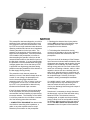
ORTEC MODEL 142AH PREAMPLIFIER
1. DESCRIPTION
The ORTEC 142AH Preamplifier is a chargesensitive unit that is designed for use with roomtemperature-operated
silicon
surface-barrier
detectors. It has been designed to give the ultimate
in both energy and timing resolution, with no
compromise through either output circuit. The
142AH Preamplifier is compatible with detectors
that have a capacitance in the range from 0 to 100
pF. It can operate with higher capacitances that
are slightly degraded. The 142AH has a low-noise
intercept and a moderate slope.
A differentiated timing output is directly compatible
with most timing applications. The typical ORTEC
modules that can use the timing signals from the
142AH include the 436 100-MHZ Discriminator, 454
Timing Filter Amplifier, 473A Constant-Franction
Discriminator, and 574 Timing Amplifier.
The energy range expected in typical applications
is from 0 to 200 MeV. Two simultaneous outputs
are provided; the output marked E is for energy
measurements and the output marked T is for
timing applications. Either or both outputs may be
used as desired, since their circuits are isolated
from each other. For best results, however, the T
output should be terminated in 50 when not in
use.
A bias circuit is included to accept the operating
voltage required by the surface-barrier detector.
The bias input circuit in the preamplifier includes a
100-M load resistor, and any detector leakage
current will have to pass through this high
resistance. A voltage drop is expected across this
load resistor, proportional to the detector leakage,
and this must be added to the bias valve for the
detector when adjusting the supply level.
An input protection circuit is built into the
preamplifier circuits to protect the input FET from
any large transient voltages that would otherwise
damage the transistor. This is discussed in the
Notice on page vi. The protection circuit also
provides a damping resistance on the input so that
relatively long cable lengths can be used between
the detector and preamplifier without disrupting the
system stability.
An internal rise time compensation adjustment is
accessible through a hole in the case of the unit.
See Section 4.5 for adjustment information.
If it is necessary to remove the cover for any
reason, observe the following instructions carefully
to prevent serious injury to yourself and/or damage
to the instrument.
Observe the steps that are included in the
Notice on page vi to discharge the high
voltage to prevent shock; the voltage levels
that are used are lethal and the capacitors
are very high quality and retain a charge
much longer than is normally expected.
Do not touch the high-megohm resistors, R4
and R7, with your bare fingers; the presence
of skin oil can reduce the resistance of the
component
and
alter
operating
characteristics.
See Section 4 for instructions that involve the
protection circuit.
2
2. SPECIFICATIONS
2.1. PERFORMANCE
NOISE Based on silicon equivalent of = 3.6 eV at
2 = 2 µs. (See Fig. 2.1.)
Detector
Capacity
(pF)
0
20
50
100
Typical
Noise
(keV)
Maximum Noise
Guaranteed
(KeV)
1.55
1.73
2.23
3.25
1.75
3.6
Typical intercept, 1.55 keV.
Typical slope, 17 eV/pF.
RISE TIME Based on a +0.5-V signal through the
E output into a 93 circuit and measured from
10% to 90% of peak amplitude; rise time
adjustment optimized; 5 ns at 0 pF, 12 ns at
100 pF.
CONVERSION GAIN Nominal, measured
through the E output, 45 mV/MeV.
INTEGRAL NONLINEARITY Measured through
the E output, 0.05% for 0 to ±7 V open circuit, or
±3.5 V terminated.
TEMPERATURE INSTABILITY <±50 ppm/(C,
0 to 50(C.
DETECTOR BIAS ISOLATION
±5000V.
OPEN LOOP GAIN 40,000.
2.2. INPUTS
INPUT Accepts input signals from
semiconductor charged-particle detector and
extends operating bias to the detector.
BIAS Accepts the detector bias voltage from a
power supply.
TEST Accepts input voltage pulses from a pulse
generator for instrument and system calibration;
Rin = 93.
Fig. 2.1. 142AH Typical Noise (0.5 )s).
2.3. OUTPUTS
E Furnishes the output signals through Ro = 93 for energy measurements; polarity is opposite
from input pulse polarity (Fig. 2.4.).
T Furnishes a differentiated output signal
compatible with typical 50 timing system
requirements; polarity is the same as the input
pulse polarity.
2.4. CONNECTORS
INPUT AND BIAS
Type SHV.
TEST, E, AND T Type BNC.
POWER CABLE 10-ft (3-m) captive power
cable (ORTEC 121-C1); longer lengths available
from ORTEC on special order.
3
2.5. ELECTRICAL AND MECHANICAL
POWER REQUIRED Furnished from any NIM
bin and power supply through any ORTEC main
amplifier or from an ORTEC 114 Power Supply;
built-in captive cable is compatible with either
source.
+24 V, 30 mA; -24 V, 1 0 mA;
+12 V, 15 mA; -12 V, 15 mA.
DIMENSIONS 1.75 X 5.2 X 4 in., plus 10-ft cable.
(4.45 X 13.2 X 10 cm, plus 3-m cable.)
3. INSTALLATION
3.1. CONNECTION TO DETECTOR
A direct connection with the shortest possible
length of shielded cable should be made between
the detector and the Input connector on the
preamplifier. For best results, the length of this
cable must be as short as possible to minimize
the preamplifier noise (due to the capacitive
loading of the cable) and to maintain the stability
of the preamplifier. The complex impedance
presented to the preamplifier input that is due to
transmission line effects acting on the detector
system impedance can disrupt the stability of the
whole system. Due to vagaries in the detector
system, a definite maximum length cannot be
specified but is typically 60 inches (150 cm).
Type RG-62/U cable is recommended for the
detector to preamplifier connection; this is 72 cable with a capacity of 21 pF/ft.
When operating at bias levels greater than 3 kV,
special care must be taken to minimize spiking
due to corona discharge from the type SHV
connectors on the able between the detector and
the preamplifier. Normally, corona problems in
the bias cable between the bias power supply and
the preamplifier are significant due to the filtering
circuit within the preamplifier.
After the input cable has been installed, the
electronic noise performance of the preamplifier
can be predicted by adding the capacity furnished
by the detector to the capacity of the cable. The
cable capacity can be calculated from its length
and its rated capacity per foot.
3.2. ENERGY OUTPUT CONNECTION TO
MAIN SHAPING AMPLIFIER
The E output of the preamplifier can be used to
drive a long 93 Iine to a shaping main amplifier
and is designed to be directly compatible with
ORTEC main amplifiers. It can be used with any
shaping main amplifier if a power supply is also
used to furnish the preamplifier power
requirements that are available on all ORTEC
main amplifiers.
3.3. TIMING OUTPUT CONNECTION TO
TIMING MODULES
The T output of the preamplifier can be used to
drive a long, terminated 50 cable to a timing
module. Typical timing modules include
amplifiers, fast discriminators, or a time-toamplitude converters. When the T output is not
being used, it should be terminated in 50 .
3.4. INPUT OPERATING POWER
Power for the 142AH Preamplifier is supplied
through the captive power cord and 9-pin
Amphenol connector. This connector can be
attached to the mating power connector on any
ORTEC main amplifier or 114 Preamplifier Power
Supply. The preamplifier's power requirements
are added to the operating power, requirements of
the amplifier or power supply to which it is
connected.
4
3.5. TEST PULSE
3.7. CORONA ELIMINATION
A voltage test pulse for energy calibration can be
accepted through the Test input connector on the
142AH without the use of an external charge
terminator. The Test input of the preamplifiers
has an input impedance of 93 , and its circuitry
provides charge injection to the preamplifier
input. The shape of this pulse should be a fast
rise time (less than 40 ns) followed by a slow
exponential decay back to the baseline (200 to
400 µs). While test pulses are being furnished to
the Test input, connect either the detector (with
bias applied) or its equivalent capacitance to the
Input connector on the 142AH.
Because the normal range of bias voltages that
are used for the detectors appropriate to the
142AH are extremely high, dust particles that
settle within the Input connector tend to cause
spiking when the high voltage is applied. The
effect can be observed directly at the E output
connector on the 142AH with no input signal.
Figure 3.1 shows the typical output signal with
large noise spikes due to a "dirty" Input connector.
This can usually be eliminated, so that the output
has an appearance like Fig. 3.2, by disconnecting
the input cable (with the protection circuit
installed) and blowing out the inner surfaces of
the SHV connector with the "corona blower" that
is furnished with the 142AH. In particularly
stubborn cases, an orderly procedure must be
used to determine the cause of spiking; a
recommended procedure is as follows:
The Test input may be used in conjunction with a
pulser such as the ORTEC 419 or 448 to calibrate
the preamplifier E output amplitude in terms of
energy or for multichannel analyzer calibration.
However, due to stray coupling between the test
circuit and other portions of the preamplifier
circuitry, the transient performance of the
preamplifier is best determined by connecting the
actual detector signal through the Input connector
instead of using the pulse generator signals.
A voltage test pulse for transient response in the
142AH can be accepted through a charge
terminator and into the Detector Input connector.
If external capacitance is to be included for these
tests, an SHV tee can be inserted between the
Input connector and the charge terminator, and
this will then accommodate the test capacitances.
Do not furnish any bias during these tests.
3.6. DETECTOR BIAS INPUT
Operating bias for the detector is supplied to the
Bias connector on the 142AH and through a filter
and large bias resistance to the Input signal
connector. From there it is furnished out through
the signal input cable to the detector.
Connect a cable from the detector bias supply
(ORTEC 459 is typical) to the Bias connector on
the 142AH. The connectors used in this highvoltage circuit are type SHV, and the mating
cable should be furnished with the bias supply
module
1. With no cable connected to the preamplifier
Input, operate the preamplifier at the desired bias
voltage while observing the E output, through a
shaping amplifier, with an oscilloscope.
2. If spiking is present, blow out the Input
connector with the blower several times until the
spiking disappears.
3. Attach the input cable from the detector. If
spiking appears, disconnect the cable and blow
out the inner surfaces of the high-voltage
connectors. Then attach the cable again and
check for spiking.
4. Apply this procedure to the connectors of each
individual cable section that has high-voltage
connectors.
5. In laboratory areas that are particularly dusty,
this procedure may have to be repeated several
times to completely eliminate all traces of spiking.
.
5
4. OPERATION
4.1. GENERAL
Figure 4.1 is a simplified block diagram of the
circuits in the 142AH Preamplifier. When the
protection circuit is in, the diode between the two
series input resistors to the amplifier stage is
connected. When the protection circuit is out, the
diode is disconnected and a jumper is used to
short across the two series input resistors.
4.2. DETECTOR BIAS
The amount of bias required by the detector is
specified in the data furnished with the detector.
The bias accepted into the preamplifier through
the SHV Bias connector is furnished through the
load resistance (approximately 100 megohms) to
the Input SHV connector of the preamplifier. If
the detector leakage current is appreciable, a
notable voltage drop will occur across the series
load resistor in the preampliflier, and this must be
added to the detector requirement when the bias
supply level is adjusted.
When the detector bias must be raised to a level
greater than 3000V, there are inherent problems
associated with obtaining low noise and high
performance. Careful design and good
manufacturing control, as well as extensive
testing under full bias, assure that each
preamplifier is free from spiking problems and
that no degradation of noise performance will
result when the required bias voltage is applied.
But dust, dirt, and other surface contamination
can collect within the Input connector and cause
spiking problems due to corona discharge in the
Input connector and associated cabling. This is
especially true when the contamination occurs on
the voltage-carrying center pin of the Input
connector while the preamplifier is operating with
bias voltages greater than 3000 V. These
problems can usually be cured by directing a
stream of clean compressed air or nitrogen into
the end of the connector to blow off the surface
contamination. This is a very subtle problem
source because enough contamination can
reaccumulate on the Input connector within
several seconds after cleaning and cause
recurrence of the corona. A dust cap is provided
to keep the Input connector covered when it is not
in use, and this will protect the interior surfaces
when a cable is not connected. When the cable is
connected, it can also transfer contaminants to
the connector that can cause some spiking
problems, even after the cable is removed.
6
Fig. 4.1. Simplified Block Diagram of the ORTEC 142AH Preamplifier.
The corona blower that is furnished with the
142AH can be used to flush the interior connector
surfaces with air when corona effects are
observed. It can be used on both the Input
connector on the preamplifier and on the
connectors of the cables that are to be attached.
It can also be used to clean the connectors at the
detector end of the input cable. Simply insert the
glass tube into the connector and squeeze the
bulb to blow air into the connector.
With the protection circuit in, the input cable can
be removed and reconnected without catastrophic
damage to the preamplifier, but the user must be
cautious to prevent touching the interior of the
connector with anything other than a good
insulator, such as the glass tube of the blower;
lethal high voltages are present on the center pin
of the Input connector under these conditions.
4.3. ENERGY OUTPUT
The charge-sensitive loop is essentially an
operational amplifier with a 1-pF capacitive
feedback. The conversion gain is nominally 45
mV/MeV, and can be increased by decreasing the
value of the feedback capacity but a subsequent
increase in rise time will result. The upper limit
on the conversion gain is the stray capacity in the
circuit with C4, the 1-pF capacitor, is removed
completely. The stray capacity is about 0.1 to 0.2
pF. If less conversion gain is desired, the value of
the feedback capacity can be increased, but this
may affect the stability of the preamplifier. The
maximum recommended additional capacity is
1.5 pF.
The energy output signal from the preamplifier is
a fast-rise-time voltage step with an exponential
return to the baseline is about 500 µs. The
polarity of the E output signals is inverted from
the signal polarity at the detector output. When
the (normal) positive bias polarity is used for the
detector, the detector output pulses are negative
and the E output of the preamplifier is positive, as
shown in Fig. 4.2.
4.4. TIMING OUTPUT
As indicated in Fig. 4.1, the T output from the
preamplifier is a transformer differentiated and
inverted version of the E output. This
differentiation removes low-frequency noise for
better timing results. Due to the differentiation of
the charge loop output, any overshoot present will
appear to increase the rise time of the timing
output as shown in Fig. 4.3. This, however, does
not affect typical timing experiment results since
it is the initial slope of the waveform that carries
the information of importance in timing. Similarly,
7
Fig. 4.2. Typical Simultaneous E and T Output
Signals.
due to slewing effects and large signal bandwidth
considerations within the charge loop, the largesignal rise time is slightly longer than that
specified at the E output for an amplitude of 1.0V
unterminated (0.5 V terminated). Again, however,
this has no impact on a typical timing experiment
since the slope of the leading edge is maintained
over the whole dynamic range of the preamplifier,
and since discriminator thresholds are typically
set well below 1.0 V.
In Fig. 4.2, the rise time of the T output appears
to be longer than that for the E output but this is
not necessarily true. The 10% and 90% check
points on the E rise time are based on the Efinal
level, which is less than the initial overshoot. On
the other hand, the 10% and 90% check points on
the T rise time are based on the peak level of the
initial overshoot, which is relatively more than the
final value for the E output.
4.5. COMPENSATION ADJUSTMENT
A bandwidth compensation adjustment is
accessible to the user of the 142AH. This control
can be adjusted through the bottom of the case
without opening the unit. It is used to tune the
preamplifier to the particular detector that is
connected in order to provide the fastest optimal
rise time of the T and E output signals for the best
Fig. 4.3. Output Rise Time Measurement.
timing resolution when the rise time is optimized
with this control. Because of the high voltages
that are present inside the case when the
preamplifier is operating, a small plastic
screwdriver or a TV tuning tool should be used for
this adjustment.
CAUTION
Do not use a metal screwdriver for this
adjustment; there is a possibility of high-bias
voltage leakage on the printed circuit that could
cause a shock.
When the 142 AH Preamplifier is shipped from
the factory, the compensation adjustment has
been set for the specified rise time resolution for
a 0-pF input capacity. For optimum results for
other input capacities, the control should be
adjusted under actual operating conditions.
If the control has been adjusted for optimum
bandwidth for a specific input capacity and the
input circuit is then changed to provide less
capacity, control readjustment is necessary so
that the preamplifier will not oscillate. If the input
capacity is increased from the value for which the
adjustment has been made, the preamplifier
should be stable and should not oscillate.
8
4.6. INPUT PROTECTION
A provision is built into the preamplifier to protect
the input FET stage from damage when highvoltage transients are applied to its input. These
transients can result from any one or more of
many causes, including detector breakdown,
moisture condensation on the input connector,
short circuits or uncharged capacitance
connected across the input while bias is being
applied through the preamplifier, or disconnection
of a bias voltage without first reducing it gradually
to zero.
The protection circuit is installed in the
preamplifier when the unit is shipped from the
factory. Although it offers protection to the FET, it
also causes some degradation of the noise
performance of the preamplifier, which increases
as detector capacity increases.
In order to take full advantage of the rise time
capabilities of the 142AH for timing experiments
(typical rise times of 4 to 10 ns for detector
capacities of 1 to 100 pF), the total cable length
should be kept as short as possible even though it
is terminated. Due to vagaries in the scattering
chamber system - ground loops, stray
inductances, etc. - and since the maximum cable
length is a factor in the input capacitance to the
preamplifier, it is not possible to give absolute
numbers. Generally, two feet is a typical
maximum length to obtain fastest rise times for
low-detector capacities. Of course, the system
can be compensated for cable lengths of up to 5
or 6 feet but slower rise times will be obtained.
The screwdriver adjustment inside the case can
be used for this type of system. The rise times
under these conditions will be in the range of 10
to 25 ns for capacitances from 1 to 100 pF.
Typical results are shown in Fig. 4.4.
With the protection circuit in, the collector lead of
Q11 is attached to the center tap of the two series
input resistors to the FET, R39 and R5. Transistor
Q11 is connected as a diode, with both the base
and the emitter tied through R8 to ground. This
prevents the voltage in the input circuit from
increasing beyond the safe limit for the FET input.
To take the protection circuit out, simply remove
the collector lead of Q11 from its circuit
connection and install a wire jumper across R39
and R5.
Inherent to all high-speed charge-sensitive
preamplifiers is the problem of keeping the total
system stable while interconnecting the detector
and preamplifier with long cables. To help ease
this problem and permit more flexibility for
installations, the protection circuit is designed to
serve not only as a protection for the FET input
but also to terminate the input cable in a nominal
100. So it is recommended that the protection
circuit be left in the preamplifier circuits whenever
possible.
Fig. 4.4. 142AH Typical Rise Time.
9
5. MAINTENANCE INSTRUCTIONS
5.1. TESTING PERFORMANCE
As ordinarily used in a counting or spectroscopy
system, the preamplifier is one part of a series
system involving the source of particles to be
analyzed, the detector, the preamplifier, the main
amplifier, and the pulse height analyzer. When
proper results are not being obtained and tests for
proper performance of the preamplifier and the
other components are indicated, it is important to
realize that rapid and logical testing is possible
only when the individual components are
separated from the system. In proving the
performance of the preamplifier, it should be
removed from the system and be dealt with alone
by providing a known electrical signal through the
input and testing for the proper output signals with
an oscilloscope as specified in steps 1 through
10.
1. Furnish a voltage pulse to the Test connector,
as outlined in Section 3.5. The polarity of the test
pulse signal should agree with the expected
signal input polarity from a detector.
2. Using a calibrated pulser, the 142AH E output
should be inverted from the input polarity and
should have a nominal scale factor of 45 -mV
output per 1-MeV equivalent energy (Si). The T
output should have the same polarity as the
inputs with a scale factor of about 20% less than
the signals through the E output.
3. The noise contribution of the preamplifier may
be verified by two basic methods. In either case,
the normal capacity of the detector and
associated cables should be replaced by a
capacitor of equal value connected to the Input
connector. This is necessary because the noise
contribution of the preamplifier is dependent upon
input capacity, as can be seen from the noise
specifications given in Section 2. The only
meaningful statement of the noise level of the
preamplifier is one that relates to the spread
caused by the noise in actual spectra. This can be
measured and expressed in terms of the full width
at half maximum (FWHM) of a monoenergetic
signal after passing through the preamplifier and
main amplifier system.
The noise performance referenced in Section 2 is
stated in these terms, and verification methods
will be described. If desired, the preamplifier can
be tested with no external capacity on the Input
connector, in which case the noise width should
be approximately that shown for zero external
capacity. In any case, the input connector and
capacitors, when used, should be completely
shielded electrically. A wrapping of aluminum foil
around the Input connector or a shielding cap
attached to the connector will suffice for testing at
zero capacity.
4. The preamplifier must be tested in conjunction
with an associated main amplifier that provides
the required pulse shaping. The typical noise
performance given in Section 2 is obtained using
an ORTEC 472A Spectroscopy Amplifier on
which the time constants have been set as
specified. For comparison of these tabulated
values, it is preferable to test the preamplifier
under identical pulse-shaping conditions. It is also
important to ensure that the noise level of the
input stage of the associated main amplifier does
not contribute materially to the total noise. This is
usually no problem provided that input
attenuators, if any, on the main amplifier are set
for minimum attenuation.
5. If a multichannel analyzer is used following the
main amplifier, testing of the noise performance
can be accomplished by merely using a calibrated
test pulse generator with charge terminator, as
outlined in step 1. With only the charge terminator
connected to the Input of the 142, the spread of
the pulser peak thus analyzed will be due only to
the noise contribution of the preamplifier and
main amplifier. The analyzer can be calibrated in
terms of keV per channel by observing two
different pulser peaks of known energy, and the
FWHM of a peak can be computed directly from
the analyzer readout.
6. It is also possible to determine the noise
performance of the preamplifier by the use of a
wide-bandwidth rms ac voltmeter such as the
Hewlett-Packard 3400A, reading the main
amplifier output noise level and correlating with
the expected pulse amplitudes per keV of signal
under the same conditions. Again, a calibrated
test pulse generator is required for an accurate
measurement.
10
In this method the preamplifier and main amplifier
are set up as they would be used normally, but
with a dummy capacitor (or no capacity) on the
Input connector of the 142AH, and with the ac
voltmeter connected to the main amplifier output.
The noise voltage indicated on the meter,
designated Erms, is read and noted. Then a test
pulse of known energy, Ein (in keV), is applied to
the Input and the amplitude of the resulting output
pulse, Eout is measured in volts with an
oscilloscope. The noise spread can then be
calculated from the formula
where Erms is output noise in volts on the 3400A
meter, Ein is input signal in keV particle energy,
and Eout is output signal in volts corresponding to
the above input. If the gain of the shaping
amplifier is adjusted so that the output pulse
height is 2.35 V for an input of 1 MeV equivalent
charge, then the rms meter will be calibrated
directly in energy (1 mV = 1 keV).
7. The noise performance of the preamplifier, as
measured by these methods, should not differ
significantly from that given in the specifications
in Section 2.
8. lf, during testing of the preamplifier and
detector, the noise performance of the
preamplifier has been verified as outlined in the
preceding section or is otherwise not suspected, a
detector may be tested to some extent by
duplicating the noise performance tests with the
detector connected in place and with normal
operating bias applied. The resulting combined
noise measurement, made either with an analyzer
or by the voltmeter method, indicates the sum in
quadrature of the separate noise sources of the
amplifier and the detector. In other words, the
total noise is given by
(Ntot)2 = (Ndet)2 + (Namp)2.
9. Each quantity is expressed in keV FWHM. The
quantity Ndet is known as the "noise width" of the
detector, and is included as one of the specified
parameters of each ORTEC semiconductor
detector. By use of the above equation and with a
knowledge of the noise of the preamplifier, the
noise width of the detector can be determined.
The significance of this noise width in evaluating
the detector is subject to interpretation, but
generally the actual resolution of the detector for
protons or electrons will be approximately the
same as the noise width; the resolution of the
detector for alpha particles will be poorer than the
noise width. The most useful application of
determining the noise width of a detector is in the
occasional monitoring of this quantity to verify
that the detector characteristics have not
undergone any significant change during use.
10. Use an ORTEC 419 Precision Pulse
Generator with a matched charge termination to
measure the rise time of the 142AH through the T
(timing) or E (energy) output. Connect the 419
output through the charge terminator to the Input
on the 142AH and use an oscilloscope with a fast
rise time (1 ns if possible). The rise time of the
preamplifier can then be computed by:
(Total rise time)2 = (Preamp rise time)2
+ (Pulser rise time)2 + (Oscilloscope rise time)2.
The rise time of the 419 is typically 3 ns.
5.2. CLEANING
If it is necessary to clean the components and/or
the printed circuit in the 142AH at any time, use
only methanol as a cleaning solvent. Do not use
compressed air or other source of pressurized gas
unless it is known to be clean and free of
compressor oil, and do not use any cleaning
agent other than methanol.
5.3. FACTORY REPAIR
This instrument can be returned to ORTEC for
service and repair at a nominal cost. Our
standard procedure for repair ensures the same
quality control and checkout that are used for a
new instrument. Always contact the Customer
Service Department at ORTEC, (865) 482-4411,
before sending in an instrument for repair to
obtain shipping instructions and so that the
required Return Authorization Number can be
assigned to the unit. Write this number on the
address label and on the package to ensure
prompt attention when it reaches the factory.