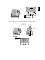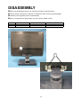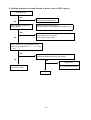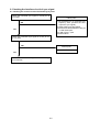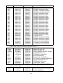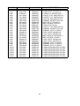
1
PART NO. 599910613
SERVICE MANUAL
COLOR MONITOR
MODEL
LCD1501
LCD1501-BK(B)
NEC-MITSUBISHI ELECTRIC VISUAL SYSTEMS CORPORATION
NOVEMBER 2002
200211
08R390B3
WARNING
The SERVICE PERSONNEL should have the appropriate technical training, knowledge and experience
necessary to:
• Be familiar with specialized test equipment, and
• Be careful to follow all safety procedures to minimize danger to themselves and their coworkers.
To avoid electrical shocks, this equipment should be used with an appropriate power cord.
This equipment utilized a micro-gap power switch. Turn off the set by first pushing power switch. Next,
remove the power cord from the AC outlet.
To prevent fire or shock hazards, do not expose this unit to rain or moisture.
This symbol warns the personnel that un-insulated voltage within the unit may have sufficient
magnitude to cause electric shock.
This symbol alerts the personnel that important literature concerning the operation and
maintenance of this unit has been included.
Therefore, it should be read carefully in order to avoid any problems.
PRODUCT SAFETY CAUTION
1. When parts replacement is required for servicing, always use the manufacturer's specified replacement.
2. When replacing the component, always be certain that all the components are put back in the place.
3. As for a connector, pick and extract housing with fingers properly since a disconnection and improper
contacts may occur, when wires of the connector are led.
4. Use a proper screwdriver. If you use screwdriver that does not fit, you may damage the screws.
CONTENTS
Page No.
USER'S MANUAL ------------------------------------------------------------------- 1-1
SERIAL NUMBER INFORMATION --------------------------------------------- 2-1
DISASSEMBLY ----------------------------------------------------------------------- 3-1
ADJUSTMENT PROCEDURES -------------------------------------------------- 4-1
INSPECTION --------------------------------------------------------------------------- 5-1
TROUBLE SHOOTING ------------------------------------------------------------- 6-1
CIRCUIT DESCRIPTION ----------------------------------------------------------- 7-1
REPLACEMENT PARTS LIST --------------------------------------------------- 8-1
BLOCK DIAGRAM ------------------------------------------------------------------- 9-1
SCHEMATIC DIAGRAMS -------------------------------------------------------- 10-1
User's Manual
LCD1501
User’s Manual
UÏivatelská pfiíruãka
Bedienerhandbuch
Οδηγίες Χρήσης
Manual del usuario
Manuel Utilisateur
Manuale utente
Gebruikershandleiding
Podr´cznik u˝ytkownika
Руководство пользователя
Kullan∂c∂ Klavuzu
1-1
For the Customer to use in U.S.A. or Canada
Canadian Department of Communications Compliance Statement
DOC: This Class B digital apparatus meets all requirements of the Canadian Interference-Causing Equipment Regulations.
Cet appareil numérique de la classe B respecte toutes les exigences du Règlement sur le matériel brouiller du Canada.
C-UL: Bears the C-UL Mark and is in compliance with Canadian Safety Regulations according to CSA C22.2 No. 950.
Ce produit porte la marque ‘C-UL’ et se conforme aux règlements de sûrele Canadiens selon CAN/CSA C22.2 No. 950.
FCC Information
1.
Use the attached specified cables with the LCD1501 colour monitor so as not to interfere with radio and television
reception.
(1)
The power supply cord you use must have been approved by and comply with the safety standards of U.S.A.,
and meet the following condition.
Power supply cord
Length
Plug shape
Non shield type, 3-conductor
1.8 m
U.S.A
(2)
2.
Shielded video signal cable. Use of other cables and adapters may cause interference with radio and television
reception.
This equipment has been tested and found to comply with the limits for a Class B digital device, pursuant to part 15 of
the FCC Rules. These limits are designed to provide reasonable protection against harmful interference in a residential
installation. This equipment generates, uses, and can radiate radio frequency energy, and, if not installed and used in
accordance with the instructions, may cause harmful interference to radio communications. However, there is no
guarantee that interference will not occur in a particular installation. If this equipment does cause harmful interference
to radio or television reception, which can be determined by turning the equipment off and on, the user is encouraged
to try to correct the interference by one or more of the following measures:
•
Reorient or relocate the receiving antenna.
•
Increase the separation between the equipment and receiver.
•
Connect the equipment into an outlet on a circuit different from that to which the receiver is connected.
•
Consult your dealer or an experienced radio/TV technician for help.
If necessary, the user should contact the dealer or an experienced radio/television technician for additional
suggestions. The user may find the following booklet, prepared by the Federal Communications Commission, helpful:
“How to Identify and Resolve Radio-TV Interference Problems.” This booklet is available from the U.S. Government
Printing Office, Washington, D.C., 20402, Stock No. 004-000-00345-4.
1-2
TCO’99
Congratulations! You have just purchased a
TCO’99 approved and labeled product! Your
choice has provided you with a product developed
for professional use. Your purchase has also
contributed to reducing the burden on the
environment and also to the further development
of environmentally adapted electronics products.
Lead**
Lead can be found in picture tubes, display screens, solders and
capacitors. Lead damages the nervous system and in higher
doses, causes lead poisoning.
TCO’99 requirement permits the inclusion of lead since no
replacement has yet been developed.
Cadmium**
Why do we have environmentally labelled computers?
Cadmium is present in rechargeable batteries and in the
colourgenerating layers of certain computer displays. Cadmium
damages the nervous system and is toxic in high doses.
TCO’99 requirement states that batteries, the colourgenerating
layers of display screens and the electrical or electronics
components must not contain any cadmium.
In many countries, environmental labelling has become an
established method for encouraging the adaptation of goods and
services to the environment. The main problem, as far as
computers and other electronics equipment are concerned, is that
environmentally harmful substances are used both in the products
and during the manufacturing. Since it has not been possible for
the majority of electronics equipment to be recycled in a
satisfactory way, most of these potentially damaging substances
sooner or later enter Nature.
There are also other characteristics of a computer, such as energy
consumption levels, that are important from the viewpoints of both
the work (Internal) and natural (external) environments. Since all
methods of conventional electricity generation have a negative
effect on the environment (acidic and climate-influencing
emissions, radioactive waste, etc.), it is vital to conserve energy.
Electronics equipment in offices consume an enormous amount of
energy since they are often left running continuously.
Mercury**
Mercury is sometimes found in batteries, relays and switches,
Mercury damages the nervous system and is toxic in high
doses.
TCO’99 requirement states that batteries may not contain any
Mercury. It also demands that no mercury is present in any of
the electrical or electronics components associated with the
display unit.
CFCs (freons)
CFCs (freons) are sometimes used for washing printed circuit
boards. CFCs break down ozone and thereby damage the
ozone layer in the stratosphere, causing increased reception on
Earth of ultraviolet light with consequent increased risks of skin
cancer (malignant melanoma).
The relevant TCO’99 requirement; Neither CFCs nor HCFCs
may be used during the manufacturing and assembly of the
product or its packaging.
What does labelling involve?
This product meets the requirements for the TCO’99 scheme
which provides for international and environmental labelling of
personal computers. The labelling scheme was developed as a
joint effort by the TCO (The Swedish Confederation of Professional
Employees), Svenska Naturskyddsforeningen (The Swedish
Society for Nature Conservation) and Statens Energimyndighet
(The Swedish National Energy Administration).
The requirements cover a wide range of issues: environment,
ergonomics, usability, emission of electrical and magnetic fields,
energy consumption and electrical and fire safety.
The environmental demands concern restrictions on the presence
and use of heavy metals, brominated and chlorinated flame
retardants, CFCs (freons) and chlorinated solvents, among other
things. The product must be prepared for recycling and the
manufacturer is obliged to have an environmental plan which must
be adhered to in each country where the company implements its
operational policy. The energy requirements include a demand that
the computer and/or display, after a certain period of inactivity,
shall reduce its power consumption to a lower level in one or more
stages. The length of time to reactivate the computer shall be
reasonable for the user.
Labelled products must meet strict environmental demands, for
example, in respect of the reduction of electric and magnetic fields,
physical and visual ergonomics and good usability.
*Bio-accumulative is defined as substances which accumulate
within living organisms.
**Lead, Cadmium and Mercury are heavy metals which are
Bio-accumulative.
To obtain complete information on the environmental criteria
document, order from:
TCO Development Unit
SE-114 94 Stockholm
SWEDEN
FAX Number: +46 8 782 92 07
E-mail (Internet): [email protected]
You may also obtain current information on TCO’99 approved
and labelled products by visiting their website at:
http://www.tcodevelopment.com
Environmental Requirements
Flame retardants
Flame retardants are present in printed circuit boards, cables,
wires, casings and housings. In turn, they delay the spread of fire.
Up to thirty percent of the plastic in a computer casing can consist
of flame retardant substances. Most flame retardants contain
bromine or chloride and these are related to another group of
environmental toxins, PCBs, which are suspected to give rise to
severe health effects, including reproductive damage in fisheating
birds and mammals, due to the bioaccumulative* processes.
Flame retardants have been found in human blood and
researchers fear that disturbances in foetus development may
occur.
TCO’99 demand requires that plastic components weighing more
than 25 grams must not contain flame retardants with organically
bound chlorine and bromine. Flame retardants are allowed in the
printed circuit boards since no substitutes are available.
1-3
Index
Warning, Caution ............................... English-1
Declaration ......................................... English-1
Contents ............................................. English-2
Quick Start ......................................... English-2
Controls .............................................. English-6
Recommended use ............................ English-9
Avvertenza, Attenzione ......................
Dichiarazione .....................................
Contenuto ..........................................
Guida rapida ......................................
Controlli ..............................................
Uso consigliato ...................................
Varování, Upozornûní ........................... âesky-1
Prohlá‰ení ............................................ âesky-1
Obsah .................................................. âesky-2
Rychl˘ start ........................................... âesky-2
Ovládací prvky ...................................... âesky-6
Provozní pokyny ................................... âesky-9
Waarschuwing, Let op! ................ Nederlands-1
Kennisgeving ............................... Nederlands-1
Inhoud ......................................... Nederlands-2
Snel aan de slag .......................... Nederlands-2
Besturingselementen ................... Nederlands-6
Aanbevolen gebruik ..................... Nederlands-9
Warnung, Vorsicht ............................. Deutsch-1
Erklärung ........................................... Deutsch-1
Inhalt ................................................. Deutsch-2
Kurzanleitung .................................... Deutsch-2
Bedienelemente ................................ Deutsch-6
Einsatzempfehlungen ........................ Deutsch-9
Uwagi dotyczàce zasilania monitora ....
Ostrze˝enie, Uwaga .............................
Deklaracja ............................................
ZawartoÊç opakowania ........................
Instalacja monitora ...............................
Przyciski ...............................................
Zalecenia eksploatacyjne .....................
ΠΡΟΕΙ∆ΟΠΟΙΗΣΗ, ΠΡΟΣΟΧΗ ..... Ελληνικά-1
∆ήλωση ......................................... Ελληνικά-1
Περιεχµενα ................................. Ελληνικά-2
Γρήγορη Εκκίνηση ....................... Ελληνικά-2
Πλήκτρα Ελέγχου ........................ Ελληνικά-6
Προτεινµενη Χρήση .................. Ελληνικά-9
Italiano-1
Italiano-1
Italiano-2
Italiano-2
Italiano-6
Italiano-9
Polski-1
Polski-2
Polski-2
Polski-3
Polski-3
Polski-7
Polski-9
Предупреждение, Внимание ......... Русский-1
Заявление ....................................... Русский-1
Содержимое ................................... Русский-2
Краткое руководство по
началу работы ................................ Русский-2
Органы управления ........................ Русский-6
Рекомендации по эксплуатации .... Русский-9
Advertencia, Peligro .......................... Español-1
Declaración ....................................... Español-1
Contenido .......................................... Español-2
Inicio rápido ....................................... Español-2
Controles ........................................... Español-6
Uso recomendado ............................. Español-9
D∂kkat, Uyari ....................................... Türkçe-1
Bildirim ................................................ Türkçe-1
∑çindekiler ............................................ Türkçe-2
H∂zl∂ Baµlama ...................................... Türkçe-2
Kontroller ............................................. Türkçe-6
Tavsiye Edilen Kullan∂m ...................... Türkçe-9
Avertissement, Attention .................. Français-1
Déclaration ....................................... Français-1
Sommaire ......................................... Français-2
Mise en marche rapide .................... Français-2
Commandes ..................................... Français-6
Conseils d’utilisation ........................ Français-9
1-4
English
âesky
Deutsch
Ελληνικά
Español
Français
Italiano
Nederlands
Polski
Русский
Türkçe
1-5
REFRAIN FROM OPENING THE CABINET AS THERE ARE HIGH VOLTAGE COMPONENTS INSIDE. REFER
SERVICING TO QUALIFIED SERVICE PERSONNEL.
CAUTION
RISK OF ELECTRIC SHOCK • DO NOT OPEN
CAUTION:
TO REDUCE THE RISK OF ELECTRIC SHOCK, DO NOT REMOVE COVER (OR BACK). NO USER
SERVICEABLE PARTS INSIDE. REFER SERVICING TO QUALIFIED SERVICE PERSONNEL.
This symbol warns user that uninsulated voltage within the unit may have sufficient magnitude to cause
electric shock. Therefore, it is dangerous to make any kind of contact with any part inside this unit.
This symbol alerts the user that important literature concerning the operation and maintenance of this unit
has been included. Therefore, it should be read carefully in order to avoid any problems.
Caution:
When operating the LCD1501 with a 220-240V AC power source in Europe, use the power cord provided with the monitor.
In the UK, a BS approved power cord with a moulded plug has a Black (five Amps) fuse installed for use with this equipment.
If a power cord is not supplied with this equipment please contact your supplier.
When operating the LCD1501 with a 220-240V AC power source in Australia, use the power cord provided with the monitor.
For all other cases, use a power cord that matches the AC voltage of the power outlet and has been approved by and
complies with the safety standard of your particular country.
Declaration
Declaration of the Manufacturer
We hereby certify that the colour monitor
LCD1501 (NL2501) is in compliance with
and marked with
Council Directive 73/23/EEC:
– EN 60950
Council Directive 89/336/EEC:
– EN 55022
– EN 61000-3-2
– EN 61000-3-3
– EN 55024
NEC-Mitsubishi Electric Visual
Systems, Corp.
MS Shibaura Bldg., 13-23,
Shibaura 4-chome,
Minato-Ku, Tokyo 108-0023, Japan
As an ENERGY STAR® Partner, NEC-Mitsubishi Electric Visual System Corp. has determined that this product meets the ENERGY
STAR guidelines for energy efficiency. ENERGY STAR is a U.S. registred mark.
IBM PC/XT/AT, PS/2, MCGA, VGA, 8514/A and XGA are registered trademarks of International Business Machines
Corporation.
Apple and Macintosh are registered trademarks of Apple Computer Inc.
Microsoft and Windows are registered trademarks of the Microsoft Corporation.
NEC is a registered trademark of NEC Corporation.
All other trademarks or registered trademarks are property of their respective owners.
English-1
1-6
English
WARNING
TO PREVENT FIRE OR SHOCK HAZARDS, DO NOT EXPOSE THIS UNIT TO RAIN OR MOISTURE. ALSO, DO NOT
USE THIS UNIT’S POLARIZED PLUG WITH AN EXTENSION CORD RECEPTACLE OR OTHER OUTLETS UNLESS
THE PRONGS CAN BE FULLY INSERTED.
Contents
Your new NEC LCD monitor box* should contain the following:
•
LCD1501 monitor with tilt base
•
Power Cord
•
Video Signal Cable
•
User’s Manual
•
CD ROM (includes complete User’s Manual in PDF format).
To see the User’s Manual, Acrobat Reader 4.0 must be installed on your PC.
*
Remember to save your original box and packing material to transport or ship the monitor.
Quick Start
To attach the LCD monitor to your system, follow these instructions:
1. Turn off the power to your computer.
2. Remove cable cover.
3. For PC: Connect the 15-pin mini D-SUB of the appropriate signal cable to the connector for the display card in your
system (Figure A.1). Tighten all screws.
For Mac: Connect the LCD1501 Macintosh cable adapter to the computer (Figure B.1). Attach the 15-pin mini D-SUB end
of the appropriate signal cable to the LCD1501 Macintosh cable adapter (Figure B.1). Tighten all screws.
Macintosh
Cable Adapter
(not included)
Macintosh G3 and G4
do not need a Macintosh
cable adapter
Figure B.1
Figure A.1
4. Connect the 15-pin mini D-SUB of the video signal cable to the appropriate connector on the back of the monitor
(Figure C.1).
5. Connect one end of the power cord to the LCD1501 monitor and the other end to the power outlet. Place the video signal
cable and AC power cord under the cable cover (Figure C.1). Replace cable cover.
NOTE:
Adjust the position of the cable under the cable cover to avoid damage for cable or monitor.
NOTE:
Please refer to Caution section of this manual for proper selection of AC power cord.
English-2
1-7
English
Cable Cover
Figure C.1
6. The Vacation Switch on the right side of the monitor must be turned on (Figure D.1). Turn on the monitor with the Power
Button and the computer.
NOTE:
The Vacation Switch is a true on/off switch. If this switch is on the OFF position, the monitor cannot be turned on
using the front button DO NOT switch on/off repeatedly.
Vacation Switch
Power Button
Figure D.1
7. No-touch auto adjust automatically adjusts the monitor to optimal settings upon initial setup for most timings. For further
adjustments, use the following OSM controls:
• Auto Adjust Contrast
• Auto Adjust
Refer to the Controls section of this User’s Manual for a full description of these OSM controls.
NOTE:
If you have any problems, please refer to the Troubleshooting section of this User’s Manual.
English-3
1-8
Tilt
Grasp both sides of the monitor screen with your hands and adjust the tilt as desired (Figure TS.1).
Remove Monitor Stand for Mounting
To prepare the monitor for alternate mounting purposes:
1. Disconnect all cables.
2. Place monitor face down on a non-abrasive surface (Figure R.1).
3. Remove the hinge cover (Figure R.1).
4. Remove the 4 screws connecting the monitor to the stand and lift off the stand assembly (Figure R.2) the monitor is now
ready for mounting in an alternate manner.
5. Connect the AC cord and signal cable to the back of the monitor (Figure R.3).
6. Reverse this process to reattach stand.
NOTE:
Use only VESA-compatible alternative mounting method.
Figure TS.1
Hinge cover
Non-abrasive surface
Figure R.1
English-4
1-9
English
Figure R.2
Figure R.3
7. This LCD monitor is designed for use with a flexible arm. Please use the attached screws (4pcs) when mounting. To meet
the safety requirements the monitor must be mounted to an arm which guaranties the necessary stability under
consideration of the weight of the monitor. The LCD monitor shall only be used with an approved arm (e.g. GS mark).
Replace screws
Thickness of bracket (arm)
2.0 ~ 3.2 mm
Tighten all screws
75 mm
75 mm
Specifications
4 SCREWS (M4)
(MAX depth: 8.5 mm)
If use other
screw, check
depth of hole.
Weight of LCD assembly: 2.8kg (MAX)
English-5
1-10
Controls
OSM (On-Screen-Manager) Controls
The OSM controls on the front of the monitor function as follows:
To access OSM press any of the control buttons (<, >, -, +, EXIT).
Control
Menu
EXIT
Exits the OSM controls.
Exits to the OSM main menu.
</>
Moves the highlighted area left/right to select control menus.
Moves the highlighted area up/down to select one of the controls.
-/+
Moves the bar left/right to increase or decrease the adjustment.
SELECT
Active Auto Adjust function. Enter the OSM controls.
Enter the OSM sub menu.
RESET
Resets the highlighted control menu to the factory setting.
NOTE:
When RESET is pressed in the main and sub-menu, a warning window will appear allowing you to cancel the
RESET function by pressing the EXIT button.
Brightness/Contrast Controls
BRIGHTNESS
Adjusts the overall image and background screen brightness.
CONTRAST
Adjusts the image brightness in relation to the background.
AUTO ADJUST
Adjusts the image displayed for non-standard video inputs.
Auto Adjust
Automatically adjusts the Image Position, the H. Size and Fine setting.
Position Controls
LEFT/RIGHT
Controls Horizontal Image Position within the display area of the LCD.
DOWN/UP
Controls Vertical Image Position within the display area of the LCD.
H. SIZE
Adjusts the horizontal size by increasing or decreasing this setting.
Should the “AUTO Adjust function” do not give you a satisfactory picture setting, a further tuning can be
performed using the “H.Size” function (dot clock). For this a Moiré test pattern could be used. This function
may alter the width of the picture. Use Left/Right Menu to center the image on the screen. If the H.Size is
wrongly calibrated, the result would look like on the left drawing. The image should be homogeneous.
When H.SIZE value is
wrong.
When H.SIZE value is
improved.
English-6
1-11
When H.SIZE value is
correct.
Should the “Auto Adjust function” and the “H.Size” function do not give you a satisfactory picture setting, a
fine tuning can be performed using the “Fine” function. It improves focus, clearity and image stability by
increasing or decreasing this setting.
For this a Moiré test pattern could be used. If the Fine value is wrongly calibrated, the result would look like
on the left drawing. The image should be homogeneous.
When FINE value is
wrong.
When FINE value is
correct.
Colour Control Systems
Six colour presets select the desired colour setting. (NATIVE colour preset cannot be changed.)
NATIVE
Original colour presented by the LCD panel that is unadjustable.
Tools
LANGUAGE
OSM control menus are available in seven languages.
OSM POSITION
You can choose where you would like the OSM control image to appear on your screen. Selecting OSM
Location allows you to manually adjust the position of the OSM control menu left, right, down or up.
OSM TURN OFF
The OSM control menu will stay on as long as it is use. In the OSM Turn Off submenu, you can select how
long the monitor waits after the last touch of a button to shut off the OSM control menu. The preset choices
are 10, 20, 30, 45, 60 and 120 seconds.
OSM LOCK OUT
This control completely locks out access to all OSM control functions. When attempting to activate OSM
controls while in the Lock Out mode, a screen will appear indicating the OSM controls are locked out.
To activate the OSM Lock Out function, press SELECT, then “+” key and hold down simultaneously. To deactivate the OSM Lock Out, press SELECT, then “+” key and hold down simultaneously.
RESOLUTION NOTIFIER
This optimal resolution is 1024 x 768. If ON is selected, a message will appear on the screen after
30 seconds, notifying you that the resolution is not at 1024 x 768.
HOT KEY
You can adjust the brightness and contrast directly. When this function is set to ON, you can adjust the
brightness with < or >, contrast with + or - key, while the OSM menu is off.
OFF TIMER
Monitor will automatically power-down when the end user has selected a pre-determined amount of time.
FACTORY PRESET
Selecting Factory Preset allows you to reset all OSM control settings back to the factory settings. The
RESET button will need to be held down for several seconds to take effect. Individual settings can be reset
by highlighting the control to be reset and pressing the RESET button.
English-7
1-12
English
FINE
Improves focus, clarity and image stability by increasing or decreasing this setting.
Information
DISPLAY MODE
Indicates the current display resolution and frequency setting of the monitor.
MONITOR INFO.
Indicates the model and serial numbers of your monitor.
OSM Warning
OSM Warning menus disappear with Exit button.
NO SIGNAL: This function gives a warning when there is no signal present. After power is turned on or
when there is a change of input signal or video is inactive, the No Signal window will appear.
RESOLUTION NOTIFIER: This function gives a warning of use with optimized resolution. After power is
turned on or when there is a change of input signal or the video signal doesn’t have proper resolution, the
Resolution Notifier window will open. This function can be disabled in the TOOL menu.
OUT OF RANGE: This function gives a recommendation of the optimized resolution and refresh rate. After
the power is turned on or there is a change of input signal or the video signal doesn’t have proper timing,
the Out Of Range menu will appear.
English-8
1-13
Safety Precautions and Maintenance
FOR OPTIMUM PERFORMANCE, PLEASE NOTE
THE FOLLOWING WHEN SETTING UP AND
USING THE LCD COLOUR MONITOR:
•
DO NOT OPEN THE MONITOR. There are no user serviceable parts inside and opening or removing covers may expose
you to dangerous shock hazards or other risks. Refer all servicing to qualified service personnel.
•
Do not spill any liquids into the cabinet or use your monitor near water.
•
Do not insert objects of any kind into the cabinet slots, as they may touch dangerous voltage points, which can be harmful
or fatal or may cause electric shock, fire or equipment failure.
•
Do not place any heavy objects on the power cord. Damage to the cord may cause shock or fire.
•
Do not place this product on a sloping or unstable cart, stand or table, as the monitor may fall, causing serious damage to
the monitor.
•
Do not place any objects onto the monitor and do not use the monitor outdoors.
•
The inside of the flourescent tube located within the LCD monitor contains mercury. Please follow the bylaws or rules of
your municipality to dispose of the tube properly.
Immediately unplug your monitor from the wall outlet and refer servicing to qualified service personnel under the following
conditions:
•
When the power supply cord or plug is damaged.
•
If liquid has been spilled, or objects have fallen into the monitor.
•
If the monitor has been exposed to rain or water.
•
If the monitor has been dropped or the cabinet damaged.
•
If the monitor does not operate normally by following operating instructions.
•
Do not bend power cord.
•
Do not use monitor in high temperatured, humid, dusty, or oily areas.
•
Do not cover vent on monitor.
•
If monitor is broken, do not come in contact with the liquid crystal.
•
If glass is broken. Handle with care.
CAUTION
•
Allow adequate ventilation around the monitor so that heat can properly dissipate. Do not block
ventilated openings or place the monitor near a radiator or other heat sources. Do not put anything on
top of monitor.
•
The power cable connector is the primary means of detaching the system from the power supply. The
monitor should be installed close to a power outlet which is easily accessible.
•
Handle with care when transporting. Save packaging for transporting.
CORRECT PLACEMENT AND ADJUSTMENT OF THE MONITOR CAN
REDUCE EYE, SHOULDER AND NECK FATIGUE. CHECK THE
FOLLOWING WHEN YOU POSITION THE MONITOR:
•
For optimum performance, allow 20 minutes for warm-up.
•
Adjust the monitor height so that the top of the screen is at or slightly below eye level.
Your eyes should look slightly downward when viewing the middle of the screen.
•
Position your monitor no closer than 40 cm and no further away than 70 cm from your
eyes. The optimal distance is 50 cm.
•
Rest your eyes periodically by focusing on an object at least 6 m away. Blink often.
•
Position the monitor at a 90° angle to windows and other light sources to minimize glare
and reflections. Adjust the monitor tilt so that ceiling lights do not reflect on your screen.
•
If reflected light makes it hard for you to see your screen, use an antiglare filter.
•
Clean the LCD monitor surface with a lint-free, non-abrasive cloth. Avoid using any
cleaning solution or glass cleaner!
•
Adjust the monitor’s brightness and contrast controls to enhance readability.
•
Use a document holder placed close to the screen.
•
Position whatever you are looking at most of the time (the screen or reference material) directly in front of you to minimize
turning your head while you are typing.
English-9
1-14
English
Recommended use
•
Avoid displaying fixed patterns on the monitor for long periods of time to avoid image persistence (after-image effects).
•
Get regular eye checkups.
Ergonomics
To realize the maximum ergonomics benefits, we recommend the following:
•
Use the preset Size and Position controls with standard signals.
•
Use the preset Colour Setting.
•
Use non-interlaced signals with a vertical refresh rate between 60-75 Hz.
•
Do not use primary colour blue on a dark background, as it is difficult to see and may produce eye fatigue to insufficient
contrast.
English-10
1-15
Printed on recycled paper
1-16
Serial Number Information
Refer to the serial number information shown below.
EX.) SERIAL NUMBER LABEL
Model Name : LCD1501
SERIAL NO. :
g g g g g g g g g g
Manufactured Year :
( Last digit )
Manufactured Month :
January to September
1 to
9
October
X
November
Y
December
Z
Classification code :
Discriminate by cabinet color
White : 0
Black : 1
Gray(Silver) : 2
Running number :
Notes : This running number doesn’t reset at each month.
(Example)
Jan. : 00001, 00002, 00003, ….., 01234,
Feb. : 01235, 01236, 01237, ….., 99999, 00001,
Mar. : 00002, 00003, 00004, …..
Factory Code:
NPG China factory : Y
Control Code:
For A ver. (U.S.A.) : A
For B ver. (Europe and Asia and Pacific) : B
For J ver. (Japan) : J
2-1
DISASSEMBLY
g Before you disassembly the set, turn off power and pull out the power plug.
g Use the proper screwdriver. If oversize or undersize is used, screws may be damaged.
g Assembly is the opposite process of disassembly.
g Note: If consignment the parts begins, the part number of NPG is used.
SYMBOL
1
2
Part No. for NPG
11001641
---
Part No. for NMV
79PQ5103
---
DESCRIPTION
COVER HINGE(R)
P4*12+SPW+WAS MC(NI)
1
2
3-1
SYMBOL
3
4
5
6
Part No. for NPG
----10103231
12300511
Part No. for NMV
----79PQ5102
79EN0526
DESCRIPTION
P3*8 ML(NI)
T3*16/W MC(NI)
COVER REAR ASSY(LCD1501BK
VESA,BKT
3
5
6
4
3-2
SYMBOL
7
8
9
Part No. for NPG
-------
Part No. for NMV
-------
DESCRIPTION
P3*6/W ML(NI)
4#-40T*40T*4.8HL*4.0*5-NL/W
SHIELD,COVER
7
9
8
SYMBOL
10
11
Part No. for NPG
--AM0R31ML
Part No. for NMV
--79PQ5080
DESCRIPTION
P3*8*8+SPW+WAS ML(NI)
MAIN INSERT ASSY
J601
10
J301
J101
11
3-3
SYMBOL
12
13
14
15
16
17
Part No. for NPG
------AP0R31ML
JM100021
RC900051
CN3
9
Part No. for NMV
------79PQ5081
79PQ5128
79PQ5160
16
DESCRIPTION
P3*8*8+SPW+GEAR ML(NI)
F3*8 ML(NI)
P4*6+SPW+WAS MC(NI)
POWER INSERT ASSY
INVERTER BD. T301001.00
LEAD CONNECTOR ASSY-SW BLK
12
15
17
CN1
CN2
J901
14
SYMBOL
18
19
20
21
Part No. for NPG
--AS0R31ML
10103201
RC200121
13
Part No. for NMV
--79PQ5082
79PQ5101
79PQ5162
DESCRIPTION
SCREW T3*10
SW INSERT ASSY
COVER FRONT ASSY(LCD1501B
WIRE 12P-12P L120
21
J800
20
18
19
3-4
SYMBOL
22
Part No. for NPG
---
Part No. for NMV
---
DESCRIPTION
P2.5*4 MC(NI)
22
22
SYMBOL
23
24
Part No. for NPG
--RC200131
Part No. for NMV
3A684033
79PQ5163
21
DESCRIPTION
LCD LM150X06-A3
WIRE 20P-20P L120
22
3-5
SYMBOL
25
26
27
28
29
30
Part No. for NPG
----12300841
17001241
11001621
---
Part No. for NMV
----79PQ5164
79PQ5165
79PQ5158
---
DESCRIPTION
P4*8/W (NI)
T4*6 ML(NI)
SHIELD BASE
PAD FOOT
TILE BASE
SCREW T3*10
26
28
29
27
28
30
25
3-6
SYMBOL
31
32
33
34
35
36
Part No. for NPG
11001661
14900031
11001651
11001671
11301481
11001631
31
Part No. for NMV
79PQ5112
--79PQ5111
79PQ5109
--79PQ5110
DESCRIPTION
COVER STAND REAR(BK)
HINGE UNIT
COVER STAND FRONT(BK)
COVER CABLE(BK)
PAD,HINGE
COVER HINGE(T)(BK)
32
36
34
35
7
33
3-7
ADJUSTMENT PROCEDURES
TABLE OF CONTENTS
Page
1. Application ........................................................................................................................... 4-2
2. Default setting ...................................................................................................................... 4-2
3. Basic operation .................................................................................................................... 4-2
3.1 Front control panel layout .................................................................................................. 4-2
3.2 Special key operation ......................................................................................................... 4-3
4. Adjustment ........................................................................................................................... 4-4
4.1 Measuring instruments, jigs, and tools .............................................................................. 4-4
4.2 Power-supply voltage ......................................................................................................... 4-4
4.3 Closure of the power circuit ............................................................................................... 4-4
4.4 Bias and gain control ......................................................................................................... 4-4
5. VG-819 setting values .......................................................................................................... 4-5
6. Explanations of the factory mode ........................................................................................ 4-6
4-1
1. Application
This adjustment specification shall be applied to the adjustment of the LCD1501 (Model No. NL2501).
2. Default setting
Item
Power Supply
Input Freq.
OSM
SETTING
BRIGHTNESS
CONTRAST
Color Temp.
OSM TRUN OFF
OSM LOOK OUT
Resolution notifier
OFF TIMER
OSD/OSM
SETTING
URL SETTING
HOT KEY
LANGUAGE
Condition
AC100V~240V
1024×768@75Hz
100%
50%
NATIVE
30 sec.
NO
ON
OFF
OSM
WWW.NEC-MITSUBISHI.COM
ON
ENGLISH
3. Basic operation
3.1 Front control panel layout
Power Button
Power Lamp
EXIT Button
CONTROL Button
ADJUST Button
SELECT Button
RESET Button
EXIT Button
Exits the OSM controls.
Exits to the OSM main menu.
CONTROL Button
Moves the highlighted area left/right to select control menus.
Moves the highlighted area up/down to select one of the controls.
ADJUST Button
Moves the bar left/right to increase or decrease the adjustment.
SELECT Button
Active Auto Adjust function. Enter the OSM controls.
Enter the OSM sub menu.
RESET Button
Resets the highlighted control menu to the factory setting.
4-2
3.2 Special key operation
<Factory mode>
1) Open the information tab [MODE] of the OSM menu.
2) Simultaneously press the three keys of < (left), > (right), and RESET.
3) When a message of WARNING appears, press the SELECT button to enter the factory mode.
4) Press the EXIT button to close the factory mode.
<Aging mode>
1) Make the setting not to receive input signals.
2) Simultaneously press the three keys of (+), (-), and RESET.
3) Using the < (left) and > (right) buttons, it becomes possible to changeover the screen color (white ⇔ red
⇔ green ⇔ blue).
4) Using the (+) and (-) buttons, it becomes possible to change the brightness of each color.
5) To close the aging mode, receive any signal to turn off the power supply.
4-3
4. Adjustment
4.1 Measuring instruments, jigs, and tools
The measuring instruments, jigs, and tools required at the time of the adjustment of the unit to be adjusted
shall be as specified below.
a. A signal generator that can generate an output of signal timing produced by the adjusted (*) VG-819 or
specified in [4. Setting method for the VG-819.] In this case, however, this signal generator shall be
capable of displaying all white and all black as a screen display pattern.
* The word “adjusted” shall mean that the amplitude of each signal R, G, B, which is output from the signal
generator, is maintained at 0.7Vp-p ± 0.05V when a load of 75Ω is connected.
4.2 Power-supply voltage
INPUT : 100Vac ~ 240Vac
4.3 Closure of the power circuit
1) Connect the suitable cable of the VG-819 according to the setting mode.
2) Turn on the Power switch of the VG-819.
3) Connect the AC power cable to the unit being adjusted.
4) Turn on the Vacation switch of the unit being adjusted (seesaw switch located on the right side of the unit).
5) Turn on the Power switch of the unit being adjusted.
6) After the completion of signal discrimination, the LED is turned green.
4.4 Bias and gain control
1) Enter an input signal of 1024×768 (75Hz), in 32-gray gradation.
2) Enter the factory mode according to “3.2 Specific key operation.”
3) Press the SELECT button several times to display the [AUTO CONTRAST] adjust menu.
4) Pressing the < (left) and > (right) buttons, adjust the cursor to [AUTO CONTRAST]. When the (+) key or
the (-) key is pressed, adjustment of the bias and the gain is carried out.
5) When adjustments have been finished, press the EXIT key to close the factory mode.
4-4
5. VG-819 setting values
Signal
Mode
H
V
OUTPUT
DOT CLOCK [MHz]
TOTAL [DOT]
DISP [DOT]
SYNC PULSE [DOT]
BACK [DOT]
HDstrat [DOT]
HDwidth [DOT]
INTERLACE
TOTAL [H]
DISP [H]
SYNC PULSE [H]
BACK PORCH [H]
EQPfp [H]
EQPbp [H]
SERRATION [H]
EDP [H]
VDs [H]
VBf [H]
OUTPUT MODE
NRZ/RZ
CV
HS
VS
CS
HD
VD
RGB
HT
C
VIDEO
Set-up
Sync
VG-819
1024×768
(75Hz)
78.75
1312
1024
96
176
0
0
NON
800
768
3
28
0
0
OFF
OFF
0
0
ANALOG
NRZ
POS
POS
NEG
NEG
NEG
POS
POS
NEG
0.70V
0.00V
0.30V
PAT SEL
GRAY
CHARA
Format
1
PATTERN
Code
82
Font
16*16
Cell
16*16
Direction:0
L0:0 L1:17 L2:34 L3:51 L4:68 L5:85
L8:143 L9:159 LA:175 LB:191 LC:207
LF:255
GRAY
4-5
L6:102
LD:223
L7:127
LE:239
6. Explanations of the factory mode
ON: Accumulated time during the reception of input signals (LED:
green)
OFF: Accumulated time in the power-saving mode (LED: amber)
* The above-mentioned accumulated time (hours running) is
reset when FACTORY PRESET or the RESET + “<”,”>” keys
is pushed during a display is executed.
T_ON: Total accumulated time during the reception of input
signals (LED: green)
T_OFF: Total accumulated time in the power-saving mode (LED:
amber)
* The above-mentioned accumulated time (hours running) is
not reset even when FACTORY PRESET is executed.
F/W VERSION: Firmware version
FACTORY PRESET: All data are reset to the initial values.
It is possible to adjust the gain values of R, G, B, respectively.
It is possible to adjust the offset values of R, G, B, respectively.
AUTO CONT: No. of auto-contrast control trials conducted by the
user
AUTO ALL: No. of auto-adjustment trials conducted by the user
HOTKEY SETTING: Set at ON (Europe version) for shipment
Set at OFF (Japan version and North
America version ) for shipment
LANGUAGE SETTING: Set at EN. (Europe and North America
version) for shipment
Set at JP. (Japan version)
AUTO CONTRAST: Auto-adjustments for the gain and the bias
4-6
It is possible to change the display of OSD adjusting values.
0: Adjusting value displayed in percentage: Setting for shipment
1: Adjusting value displayed in a numeral: (Debug)
The OSD/OSM display is changed over for the OSD menu.
0: OSM (Setting for shipment)
1: OSD
Display or no display of URL (Internet address)
0: Not displayed (for Japan)
1: Displayed (WWW.NECMITSUBISHI.COM): Setting for
shipment (for North America and Europe version)
2: Displayed (WWW.NEC-MITSUBISHI.COM): Debug
This menu is not used.
It is possible to adjust the R, G, B values for each color
temperature.
4-7
Inspection
TABLE OF CONTENTS
Page
1. Electrical inspection ............................................................................................................. 5-2
1.1 Electrical performance ....................................................................................................... 5-2
1.2 Frequency change ............................................................................................................. 5-2
1.3 Performance check ............................................................................................................ 5-2
1.4 Check power manage function .......................................................................................... 5-2
2. Safety ................................................................................................................................... 5-3
2.1 Insulation resistance .......................................................................................................... 5-3
2.2 Dielectric strength .............................................................................................................. 5-3
2.3 Leakage current ................................................................................................................. 5-3
2.4 Ground continuity ............................................................................................................... 5-3
3. Preset timing sheet .............................................................................................................. 5-3
4. Inspection of PLUG & PLAY communication and OSM "MONITOR INFORMATION"
for model name/ serial number ............................................................................................ 5-4
4.1 System connection ............................................................................................................. 5-4
4.2 Input signal ......................................................................................................................... 5-4
4.3 Program ............................................................................................................................. 5-4
4.4 Operation ........................................................................................................................... 5-5
4.5 EDID data file ..................................................................................................................... 5-8
5. External inspection on the LCD module .............................................................................. 5-9
5.1 Inspection condition ........................................................................................................... 5-9
5.2 Standards for display conditions ........................................................................................ 5-9
5.3 The inspection standard of appearance .......................................................................... 5-12
5.3.1 Polarizer defects ........................................................................................................... 5-12
5.3.2 Foreign material ............................................................................................................ 5-12
5.3.3 Line defect .................................................................................................................... 5-12
5.3.4 Bezel appearance ......................................................................................................... 5-12
5-1
1. Electrical inspection
1.1 Electrical performance
Function switch check
1) Input 1024×768 (75Hz) pattern “Crosshatch”.
2) Image should appeared within 4sec after Switch ON.
3) LED lighting green.
4) It should not appear noise while Switch is turn ON or turn OFF.
5) OSM should be indicated by push [Exit] or [<] OR [>] or [-] or [+] button.
6) While [-] or [+] button is pushed, the value should change smooth and it should not be appeared noise.
7) Check the OSM off when push the [OSM OFF] switch EXIT.
1.2 Frequency change
1) Change the preset timing.
2) Check the picture and the time when freq. change (less 5 sec).
1.3 Performance check
1) Input 1024×768 (75Hz) pattern “RGB 256 GRAY SCAL” PATTERN.
2) Press [AUTO CONTRAST] switch.
3) Check the color gray scal smoth and not data lost.
1.4 Check power manage function
Mode
Horizontal
Vertical
Normal
Standby
Suspend
Off
On
Off
On
Off
On
On
Off
Off
Power
Supply
240V
240V
240V
240V
5-2
Input Timing
1024×768 (75Hz)
1024×768 (75Hz)
1024×768 (75Hz)
1024×768 (75Hz)
Power
consumption
20W
2W
2W
2W
2. Safety
2.1 Insulation resistance
The resistance of the insulation between the power terminal and the earth ground contact is more than 10M
ohms while withstanding a voltage of 500Vdc.
2.2 Dielectric strength
There is no breakdown of the insulators or short circuits when applying an alternating potential of 1000Vac
for a duration of 1(one) minute or 1500Vac for a duration of 2(two) second at 50Hz between the metallic
chassis and the input power supply active and neutral terminals connected together.
2.3 Leakage current
The current conducted between each of the power supply’s contacts is less than 1.5mA at 255Vac (60Hz)
and 0.25mA at 100Vac (60Hz).
2.4 Ground continuity
The resistance between the groundside of the power cord and the accessible metal parts located in ground
circuit shall not exceed 0.1 ohm at current load of 25mA.
3. Preset timing sheet
Horizontal
No
1
2
3
4
5
6
7
8
9
10
11
12
13
14
15
16
Timing
VGA 720×350
70Hz
PC98 640×400
56Hz
VGA 720×400
70Hz
VGA 640×480
60Hz
MAC 640×480
66Hz
VESA 640×480
72Hz
VESA 640×480
75Hz
VESA 800×600
56Hz
VESA 800×600
60Hz
VESA 800×600
75Hz
VESA 800×600
72Hz
MAC 832×624
75Hz
VESA 1024×768
60Hz
SUN 1024×768
65Hz
VESA 1024×768
70Hz
VESA 1024×768
75Hz
Dot
Freq.
Clock
(KHz)
(MHz)
Vertical
Total Active Pulse Back
Front
Freq.
(Hz)
Total Active Pulse Back
Front HS,VS
28.322 31.469
900
720
108
54
18
70.087
449
350
2
60
37
P,N
21.053 24.827
848
640
64
85
59
56.424
440
400
8
25
7
N,N
28.322 31.47
900
720
108
54
18
70.087
449
400
2
35
12
N,P
25.175 31.47
800
640
96
48
16
59.992
525
480
2
33
10
N,N
30.24
34.97
864
640
64
96
64
66.61
525
480
3
39
3
N,N
31.5
37.861
832
640
40
128
24
72.809
520
480
3
28
9
N,N
31.5
37.5
840
640
64
120
16
75.00
500
480
3
16
1
N,N
36
35.156 1024
800
72
128
24
56.25
625
600
2
22
1
P,P
40
37.879 1056
800
128
88
40
60.317
628
600
4
23
1
P,P
49.5
46.875 1056
800
80
160
16
75
625
600
3
21
1
P,P
50
48.077 1040
800
120
64
56
72.188
666
600
6
23
37
P,P
57.283 49.725 1152
832
64
224
32
74.55
667
624
3
39
1
N,N
1024
136
160
24
60.004
806
768
6
29
3
N,N
1344
1024
136
160
24
65.57
806
768
6
29
3
N,N
56.476 1328
1024
136
144
24
70.069
806
768
6
29
3
N,N
78.75 60.023 1312
1024
96
176
16
75.029
800
768
3
28
1
P,P
65
70.49
75
48.363 1344
53.7
5-3
4. Inspection of PLUG & PLAY communication and OSM "MONITOR INFORMATION"
for model name/ serial number
4.1 System connection
This system should be connected as shown below.
Program
Part No. 599910612
DC +5V
DESKTOP/NOTE
PC
Printer cable
(Jig)
Signal cable
CN5
CN3
CN7
CN6
CN4
Signal cable
DDC communication
I/F BOARD
Signal generator
Part No.599910541
DDC Communication I/F BOARD
4.2 Input signal
Horizontal synchronization frequency
: Not specified.
Vertical synchronization frequency
: Not specified.
4.3 Program
Service tool Ver. 3.14 (Parameter ver. 2.0-S2) (Part No. 599910612)
5-4
Monitor
4.4 Operation
1) Connect the EDID data writing unit with jigs, etc.
2) Copy all the files of the service tool Ver. 3.14 (Parameter ver. 2.0-S2) in a proper directory.
3) Start [Service2.EXE] of the service tool Ver. 3.14.
4) When the screen as shown below appears, give a check to [LCD] of [Monitor Type] and press the [START]
button.
5) When the screen as shown below appears, adjust the cursor to [LCD1501] and make a double click.
5-5
6) When the screen as shown below appears, give a check to [EDID_READ] and press the [OK] button.
7) When the screen as shown below appears, confirm that the correct data are displayed in the columns of
EDID DATA CONTENTS and Serial information.
If all the displayed data are [FF] or the like, or if the serial number is different from that of the corresponding
unit, then EDID data writing should be carried out.
8) When a screen of Item 6 is displayed by pressing the [BACK] button, give a check to [EDID_WRITE] and
press the [OK] button.
5-6
9) When the screen as shown below appears, examine the serial number of the unit, enter an input in the
column of [Input Serial No.] through the keyboard, and press the [Input OK] button.
Enter an input in the column of [.Year=> ] in manufactured year(A.D. four digits) and [Month=>] in
manufactured month through the keyboard, and press the [Input OK] button.
10) When the [WRITE EDID] button is pressed, writing of the EDID data only is carried out. Upon the
completion of correct writing, a display of [EDID Monitor Write OK] is presented in the column of
[STATUS].
5-7
11) Let the Power switch of the writing unit be turned OFF/ON, and examine the SERIAL NUMBER column
of the OSD [MONITOR INFO.] to see that its contents have been changed to the updated serial number.
12) Upon the normal completion of EDID data writing, press the [Exit] button to close the program.
4.5 EDID data file
EDID date: LCD1501.edi
0
1
2
3
4
5
6
7
8
9
A
B
C
D
E
F
00
00
FF
FF
FF
FF
FF
FF
00
38
A3
FB
65
01
01
01
01
10
0C
0C
01
03
08
1E
17
78
EA
B1
45
A1
58
4F
95
26
20
1D
50
54
BF
EE
00
01
01
01
01
01
01
01
01
01
01
30
01
01
01
01
01
01
C3
1E
00
20
41
00
20
30
10
60
40
13
00
30
E4
10
00
00
1E
00
00
00
FD
00
37
4B
1F
50
3C
08
00
0A
20
20
20
20
20
20
00
00
00
FC
00
4E
60
45
43
20
4C
43
44
31
35
30
31
0A
20
00
00
00
FF
70
00
32
33
30
30
30
30
31
59
58
30
0A
20
20
00
75
Note 1: address 10h
Week of manufacture = Month of manufacture × 4
Note 2: address 11h
Year of manufacture - 1990
Note 3: address 71h ~ 7Dh Serial Number (ASCII coded)
If less than 13 char, terminate with 0Ah and fill the rests with 20h.
Note 4: address 7Fh
Checksum
The sum of entire 128 byte shall be equal to 00h.
5-8
5. External inspection on the LCD module
5.1 Inspection condition
1) Ambient temperature is approximately 20~25°C.
2) Ambient humidity is approximately 65 ±.
3) Ambient illuminant is from 300 to 700lux.
4) Viewing distance is approximately 35cm.
5) Viewing angle : right and left 30°, top and bottom 20° ~ 0°.
5.2 Standards for display conditions
Standard for errors (defects)
Joined
defects
(1)
(2)
(3)
(4)
Dot defect
(5)
Item
Continuous 2 bright dots
Continuous 2 black dots
Continuous 3 or more bright
dots
Continuous 3 or more black
dots
Dot defects other than (1) and
(2)
Adjacent to same-color
bright-dot defect
Approach of adjacent defects
of (6)
Defect cluster
Standard
R+G, 2 continued
≤ 2 pairs
horizontally
≤ 2 pairs
Both the same color ≤ 0 pair
and different colors
are counted.
≤ 0 pair
R.G.B (Black dot +
Bright dot)
Defective
(6)
Distance between
proximity
defects ≤ 6.5mm
(7)
Distance of approach
≤ 15mm
(8)
A set of 2 or more dot
defects in an area of
5×5 pixels
[(5) in consideration]
Approach of adjacent
defects of (1) in an
area of 5×5 pixels
Approach of adjacent
defects of (2) in an
area of 5×5 pixels
Total No.
Total No. of bright dots (R.G.B) + black dots (R.G.B)
of defects Total No. of bright points in G
Note 9. Every dot herein means sub-pixel (each Red, Green or Blue color)
Remarks
Note 1
Note 2
Note 3
≤4
Note 4
Each color ≤ 2 pairs
Note 5
≤ 0 pair
Note 6
≤ 2 clusters
Note 7
≤ 0 pair
Note 8
≤4
≤4
-
Note 10. Bright & Dark Dots are larger than one third of sub-pixel. (Dots smaller than one third of sub-pixel
are not counted as a defect dots.)
Note 11. Do not use the [ND] filter in counting a bright dot.
5-9
:Bright dot
:Black dot
Note 1: R + G, 2 dots continued horizontally
Counted as an NG
RG
RG
Not counted as NG
Combination of bright
Combination other than
and black dots
2-horizontal combination
RG
G
R
RG
R
G
and others
Note 2: (1) + (2) ≤ 3 pairs
Note 3: 3-defect combination
Combination patterns to be counted as NG / Combination of all bright or all black dots
and others
Not counted as NG / Combination of bright and black dots
and others
Note 4: The dots for composing 2-horizontal combinations of R + G shall be excluded from counting.
Note 5: Adjacent to same-color bright-dot defect
Counted as NG
R
R
≤ 6.5mm
Not counted as NG
R
R
≤ 6.5mm
Approach of bright and black dots
5-10
R
G
≤ 6.5mm
Approach of different colors
Note 6: Approach of adjacent defects
R
R
R
>10mm
R
≤ 6.5mm
≤ 6.5mm
The distance between adjacent defects shall be longer than 10mm.
Note 7: A set of 2 or more dot defects in an area of 5×5 pixels
If there are two or more dot defects [(5)] in an area of 5×5 pixels, such a set of dot defects shall be
counted as one cluster.
5×5 pixels
Dot defects [(5)]
There shall be no more than 3 clusters throughout
the screen area.
1 cluster
Note 8. Two or more pixels or sub-pixels with more than one fault of 1) or 2) within 5x5 pixels
Count as defect
5x5 pixels
RG
Do not count as defect
5x5 pixels
5x5 pixels
RG
RG
RG
RG
RG
5-11
5.3 The inspection standard of appearance
5.3.1 Polarizer defects
Items
Criteria
Scratch
Linear
0.05 ≤ W ≤ 0.2, 5.0 ≤ L ≤ 10.0, N ≤ 4
Dent
Circuar
0.2 ≤ D ≤ 0.5, N ≤ 6
NOTE:
D: Average Diameter
D=(a+b)/2
W: Width,
L: Length,
Linear: a>2b,
Circular: a<2b
N: Quantity b
Unit: mm
a
a. Extraneous substances that can be wiped out like Finger Print, Particles are not considered as a defect.
b. Defects which is on the Black Matrix (outside of Active Area) are not considered as a defect.
5.3.2 Foreign material
Items
Foreign
Material
NOTE:
Criteria
Linear
0.05 ≤ W ≤ 0.1, 0.3 ≤ L ≤ 4.0, N ≤ 4
Circuar
0.2 ≤ D ≤ 0.5, N ≤ 6
D: Average Diameter
D=(a+b)/2
W: Width,
L: Length,
Linear: a>2b,
Circular: a<2b
N: Quantity b
Unit: mm
a
5.3.3 Line defect
All kinds of line defects such as vertical, horizontal or cross are not allowed.
5.3.4 Bezel appearance
Scratches, minor bents, stains, particles on the Bezel frame are not considered as a defect.
5-12
TROUBLESHOOTING
TABLE OF CONTENTS
Page
1. No display of screen (Screen is black, color of LED is amber) ........................................ 6-2
2. Nothing displays on screen (Screen is black, color of LED is green) .............................. 6-3
3. Checking the back light unit ............................................................................................. 6-6
4. Abnormal screen .............................................................................................................. 6-7
5. Abnormal plug and play operation ................................................................................... 6-8
5.1 Abnormal DDC2 ............................................................................................................. 6-8
6. Checking the interface circuit of sync signal .................................................................... 6-9
6.1 Checking the control circuit of horizontal sync pulse ..................................................... 6-9
6.2 Checking the control circuit of vertical sync pulse .......................................................... 6-10
7. Checking the resolution change IC movement ................................................................ 6-11
8. No power on ..................................................................................................................... 6-12
9. Checking the operation of CPU ........................................................................................ 6-13
6-1
1. No display of screen (Screen is black, color of LED is amber)
Does OSM display when you
push “EXIT”, “3”, “4”, “+” OR “-”
button.
YES
NO
When a signal isn't being inputted, it is indicated with "NO SIGNAL".
It is indicated with "OUT OF RANGE" at the time of the frequency that it
over spec. timing.
Check if the sync signal from Computer is output
and if the video cable is connected normally.
Proceed section 2 “Nothing
display on screen”
NG
OK
Input the sync signal of computer,
or change the cable.
Proceed section 7 “Checking the resolution
change IC movement”.
6-2
2. Nothing displays on screen (Screen is black, color of LED is green)
Is backlight lit?
NG
OK
Does computer output RGB
video signals?
NG
OK
Refer to section 3
“Checking the backlight unit.
Check the video cable for failure.
Check the host for output signal with all black only.
1) Change pattern of video signal output on the host.
2) Reconnect the video cable.
3) Change the video cable.
Check OSM menu is displayed on screen
when you push the “EXIT”, “3”, “4”, “+” OR
“-“ key.
NG
Check if the LCD video signal cable is connected
between the MAIN board and LCD module.
OK
NG
Proceed section 4
“Abnormal screen “.
Failure point
The cable is disconnected.
OK
Next page
6-3
Continue
Is 3.3V voltage provided to pins 19 and 20 of J301 in
MAIN board?
NG
Is 3.3V voltage provided to pin 19
and 20 of J301.
Failure point
NG
OK
OK
Check Q301and IC301
Failure point
J301 cable pulled out or disconnected
Is a PCLK being outputted under the condition that
R304 in main BD?
Failure point
NG
1) IC401 failure.
2) Printed wire broke between
IC401 and IC301 pin31.
3) R431;C312 or R304 failure
OK
Check the DE pulse is output on R405?
Failure point
1) IC401 failure.
2) Printed wire broke between
IC401 and IC301 pin30.
3) R405 or C313 failure
NG
OK
Failure point
Check the PVD signal is ouput on R433 ?
1) IC401 failure.
2) Printed wire broke between
IC401 and IC301 pin28.
3) R433, C314 failure.
NG
OK
next page
6-4
Continue
Failure point
Check the PHD signal is ouput on R432?
1) IC401 failure.
2) Printed wire broke between
U401 and IC301 PIN27.
3) R432 or C315 failure.
NG
OK
Check the data signal output on IC301 R,
G, B data pin?.
Failure point
1) IC401 failure.
2) Printed wire broke between
IC401, IC301 line.
NG
OK
Failure point
IC301 failure
6-5
3. Checking the back light unit
Is 12V voltage provided to inverter?
NG
Failure point
OK
Check Power Board.
Is 12V-source voltage provided
to pins 1 and 2 of CN1 in
inverter module?
NG
Failure point
OK
Inverter cable disconnection.
Check the ON/FF signal of equal “H” at CN1 pin6?
NG
1) µ-p failure.
2) printed wire broke between µ-p trace to CN1 pin6.
OK
Check Inverter F1 open.
NG
Failure point
OK
Inverter cable disconnection.
Failure point
F1 failure. Replace the
inverter board.
6-6
4. Abnormal screen
Check the R, G, B video signal from computer
input on D-Sub R,G,B connector.
Failure point
1) No R, G and B video signal output from host
computer. Check computer.
2) Video signal cable disconnection.
NG
OK
Check the R,B,G input signals on IC401 pin 2,
13, 20,respectively that their level is 0.7Vp-p
typical.
Failure point
In the case of the Red signal.(A Green and
Blue signal is the same path, too.)
Printed wire broke between D-Sub(R,G,B) and
IC401 pin 2,13,20.
NG
OK
Is the pulse of the TTL level being output to
IC301 from the data line of IC401?
Failure point
NG
Printed wire broke between IC401 data line
and IC301
OK
Check the PHD sync pulse output to IC301
pin27 from IC401 pin53 at TTL level.
Failure point
NG
OK
Printed wire broke between IC401 pin53 and
IC301 pin53.
Check the PVD sync pulse output to IC301 pin28
from IC401 pin54 at TTL level.
Failure point
NG
Printed wire broke between IC401 pin54 and
IC301pin28
OK
Check the PDE sync pulse output to IC301
pin30, from IC401 pin126 at TTL level.
Failure point
NG
Printed wire broke between IC401 pin126 and
IC301 pin30
OK
Proceed section 7 “Checking the resolution change IC
movement”.
6-7
5. Abnormal plug and play operation
Abnormal DDC2B
Confirm the output of serial data on IC101 pin26
synchronize SCLK at TTL level.
NG
Failure point
IC101 failure.
OK
Failure point
1) The host machine isn't communicating in DDC2B mode.
2) The video cable may have failed or may not to have
connections for DDC.
3) Between IC101 pin26 and J201 pin 15 may have failed.
4) Cable failure.
6-8
6. Checking the interface circuit of sync signal
6.1 Checking the control circuit of horizontal sync pulse
Check the horizontal sync signal on IC203 pin3 at
TTL level.
Failure point
1) No separate sync or composite sync
output by host. (Confirm the host,
output the sync signal.)
2) Video cable may have failed.
3) Printed wire broke between J201 pin
13 and IC203 pin3.
4) L208 or R211. open
5) IC203 failure.
NG
OK
Check the hovizuntal sync signal on IC401 pin141
a TTL level.
NG
Failure point
IC401 failure
OK
Procees section 7 “Checking the resolution change
IC movement”
6-9
6.2 Checking the control circuit of vertical sync pulse
Check the vertical sync signal on IC203
pin9 at TTL level.
Failure point
NG
OK
1) No separate sync output signal from the host.(Check the
host.)
2) Video cable may have failed.
3) Printed wire broke between J201 pin 14 and IC203 pin9
4) L209 or R213 open.
5) IC202 failure
Proceed section 7 “Checking the resolution
change IC movement”.
6-10
7. Checking the resolution change IC movement
Is there +3.3V supply on IC401 pins 49, 57, 67, 79, 89, 101, 113, 125 ,132,143, 159. Is there
+2.5V SUPPLY ON IC401 PIN 3, 6,14,17, 21,24, 26, 32, 38, 46, 71, 91, 103,123, 145,147,
152;Is there +3.0V supply on IC401 Pin8.
NG
Proceed section 9 “Checking the
operation of CPU”
OK
Is 25MHz clock input to IC401 pin47 at TTL
level.?
NG
OK
Is 25MHz clock output from X401 at TTL level?
OK
Failure point
X401 failure
Proceed section 9 “Checking the operation
of CPU”.
6-11
8. No power on
Check the +12V power provided from Power
Board.
Failure point
NG
Power Board failure.
OK
Check 3.3V power from IC601
Failure point
NG
OK
"Checking the DC/DC
converter circuit"
Proceed section 9 "Checking the operation of
CPU "
6-12
9. Checking the operation of CPU
Is there +3.3V supply on IC101 pins 5.
NG
Failure point
OK
L110 open
Is 12MHz clock input to IC101 pin8, 9 at TTL level?
NG
OK
Failure point
X101 failure.
Failure point
IC101 failure.
6-13
CIRCUIT DESCRIPTION
TABLE OF CONTENTS
Page
1. Block diagram ...................................................................................................................... 7-2
2. power circuit ......................................................................................................................... 7-3
2.1 power input ........................................................................................................................ 7-3
2.2 DC to Dc circuit .................................................................................................................. 7-3
2.3 panel Vcc control ............................................................................................................... 7-3
3. Microprocessor control circuit .............................................................................................. 7-4
3.1 clock circuit ........................................................................................................................ 7-4
3.2 I2C buses ............................................................................................................................ 7-4
3.3 General-purpose port ......................................................................................................... 7-4
3.3.1 Key scan status ............................................................................................................... 7-4
3.3.2 scaler control ................................................................................................................... 7-4
3.3.3 Led control ...................................................................................................................... 7-4
3.3.4 Data memory .................................................................................................................. 7-4
4. Scaler ................................................................................................................................... 7-4
7-1
1. Block diagram
H
2.5V O/P
SDASCL
EEPROM
IC102
24C16
ADC
SCALER
IC401
SAA6713AH
12MHz;
X101
UP
IC101
NT68F632
3.3V
R,G,B DATA
PCLK,DE,H,V
25MHz;OSC
X401
Panel Vcc
LVDS SIGNAL
Switch
IC302
HAT1053
IC301 LVDS XMTR.
J301; TO PANEL
R,G,B
H sync.
V
IC203
V sync.
2.5V
3.3V O/P
INVERTER control signal
DC TO DC
IC601
TL494
7-2
DDC SDA
DDC SCL
12V I/P
REG.
IC402
J101; TO Key control BD
J201; DSUB connector
J601; TO Power BD
2. Power circuit
2.1 Power input
12V DC input from power Board through J601 to interface.
2.2 DC to DC circuit
IC610 is used generate the system power. It have built in 1 channel PWM controller to provide voltage
output.
The output (3.3V) is provide panel Vcc and 2.5V regulator input.
and provide the Scaler and MCU power.
2.3 Panel Vcc control
Panel power control used Q301 and IC301 from IC101 (pin35) PANELVCC_CTL.
While the PANELVCC_CTL stay at High level ;the panel voltage is 3.3V.
While the PANELVCC_CTL stay at Low level ;the panel voltage is 0V.
7-3
3. Microprocessor control circuit
3.1 Clock circuit
The X101 is crystal ;it generates an 12MHz output for microprocessor.
3.2 I2C buses
IC101 (pin 12) SDA
Serial data
IC101 (pin 13) SCL
Serial clock
2
This is I C serial communication bus and is used for READ or WRITE data communication of IC101 and
IC401.
3.3 General-purpose port
3.3.1 Key scan status
IC101 pin16 is for “POWER”
IC101 pin17 is for OSD “RESET” adjust
IC101 pin18 is for OSD “SELECT” adjust
IC101 pin19 is for OSD “+” adjust
IC101 pin20 is for OSD “-” adjust
IC101 pin21 is for OSD “4” adjust
IC101 pin22 is for OSD “3” adjust
IC101 pin23 is for OSD “EXIT” adjust
3.3.2 Scaler control
IC101 pin15 (I/O) for scaler interrupt signal.
IC101 pin14 output scaler reset signal.
3.3.3 LED control
IC101 pin 2 control Q103 for Green LED lit.
IC101 pin 3 control Q102 for RED LED lit.
3.3.4 Data memory
The display control data are held by the EEPROM (IC102) ;These display control data are accessed through
the I2C bus of the MCU.
4. Scaler
The scaler IC (IC401) is controlled by MCU through the I2C bus.
IC401 embeded the ADC provide with the analog interface input.
X401 output 25MHz fed to IC401.
IC203 schmitt trigger for sync.waveform processor. And fed to IC401 for mode detect.
7-4
REPLACEMENT PARTS LIST
The components specified for Model LCD1501
SYMBOL
Part No for NPG Part No for NMV
*** ICS ***
IC101
IC102
IC203
IC301
IC401
IC402
IC601
IC604
IC901
IC902
IC921
DESCRIPTION
EHA10341
EHA10391
EHA50011
EHA10381
EHA10061
EHA10311
EHA10331
EHA10351
EH170021
EH190021
EH190011
79PQ5134
79PQ5137
79EN0560
79PQ5136
79PQ5013
79PQ5132
79PQ5133
79PQ5135
79PQ5012
79EN0553
79EN0552
IC PLCC NT68F632 MCU 8BIT
IC SMD M24C16-WMN6 EEPROM
IC MOS 74LVC14
IC SMD THC63LVDM83R LVDS
IC SMD SAA6713AH SCALER
IC SMD MIC39100-2.5BS REG
IC SMD TL494 SO16 PWM CTL
IC SMD PQ05DZ51 SC-63 REG
IC TOP245Y HYBRID POWER
IC PHOTO COUPLE PC123Y
IC KIA431A-AT
*** TRANSISTORS ***
IC302
EQ500117
IC602
EQ500217
Q101
EN000211
Q102
EP000313
Q103
EP000313
Q203
EP000313
Q301
EN000211
Q401
EN000211
Q402
EN000211
Q403
EQ500411
Q601
EN000413
Q602
EP000313
Q603
EN000413
79EN0587
79EN0588
79EN0576
79EN0583
79EN0583
79EN0583
79EN0576
79EN0576
79EN0576
79PQ5076
79EN0578
79EN0583
79EN0578
FET CHIP HAT1053M
FET CHIP SI3457DV
TR CHIP NPN DTC114EUA
TR CHIP 2SA1037AK-T146R
TR CHIP 2SA1037AK-T146R
TR CHIP 2SA1037AK-T146R
TR CHIP NPN DTC114EUA
TR CHIP NPN DTC114EUA
TR CHIP NPN DTC114EUA
FET SMD P SI230IDS-TI
TR CHIP 2SC2412K-T146R
TR CHIP 2SA1037AK-T146R
TR CHIP 2SC2412K-T146R
*** DIODES ***
BD901
EJ000110
D201
EX500216
D202
EX500216
D203
EX500216
D204
EX700216
D205
EYD40562
D206
EYD40562
D207
EYD40562
D208
EYD40562
D209
EYD40562
D210
EYA30400
D211
EX700115
D401
EYE40301
79EN0568
79EN0594
79EN0594
79EN0594
79EN0596
79EN0598
79EN0598
79EN0598
79EN0598
79EN0598
79PQ5139
79EN0595
79PQ5028
DIODE D2SB60A
DIODE CHIP DAN217 T146
DIODE CHIP DAN217 T146
DIODE CHIP DAN217 T146
DIODE RB495D
ZD CHIP UDZS5.6B TE-17
ZD CHIP UDZS5.6B TE-17
ZD CHIP UDZS5.6B TE-17
ZD CHIP UDZS5.6B TE-17
ZD CHIP UDZS5.6B TE-17
ZD SMD HZK4A 1/2W
DIODE CHIP CRS01 C
ZD Z02W 3.0V
8-1
SYMBOL
D601
D602
D603
D605
D803
D901
D902
D921
PD901
Part No for NPG Part No for NMV
EX500114
EX700411
EYD40562
EX700411
EL200110
EJ300115
EJ100041
EJ100030
EJ100061
*** TRANSFORMERS ***
T901
HE100061
DESCRIPTION
79EN0592
79PQ5027
79EN0598
79PQ5027
79EN0573
79EN0570
79PQ5021
79PQ5020
79PQ5022
DIODE/T CHIP 1SS355TE-17
DIODE SSM24
ZD CHIP UDZS5.6B TE-17
DIODE SSM24
DIODE LED SML19460C
DIODE SF13
DI BYV26E 1A 1KV
DI FCQ10A06 10A 60V
DI P6KE200A
79PQ5061
TRANS POWER 49A-1041
*** RELAYS & SWITCHES ***
SW800
JC300111
79EN0691
SW801
JC300111
79EN0691
SW802
JC300111
79EN0691
SW803
JC300111
79EN0691
SW804
JC300111
79EN0691
SW805
JC300111
79EN0691
SW806
JC300111
79EN0691
SW807
JC300111
79EN0691
SW-TACT SKQNAED010
SW-TACT SKQNAED010
SW-TACT SKQNAED010
SW-TACT SKQNAED010
SW-TACT SKQNAED010
SW-TACT SKQNAED010
SW-TACT SKQNAED010
SW-TACT SKQNAED010
*** PWB ASSYS ***
INBD
JM100021
MANA
AM0R31ML
PWRNA
AP0R31ML
SWNA
AS0R31ML
79PQ5128
79PQ5080
79PQ5081
79PQ5082
INVERTER BD. T301001.00
MAIN INSERT ASSY
POWER INSERT ASSY
SW INSERT ASSY
*** COILS & FILTERS ***
B901
HC011012
B902
HC011012
L101
HM011011
L102
HM011011
L103
HM011011
L104
HM011011
L105
HM011011
L106
HM011011
L107
HM011011
L108
HM011011
L109
HM011011
L110
HM011011
L111
HM011011
L112
HM011691
L113
HM011691
L201
HM011102
L202
HM011102
L203
HM011102
79EN0672
79EN0672
79EN0677
79EN0677
79EN0677
79EN0677
79EN0677
79EN0677
79EN0677
79EN0677
79EN0677
79EN0677
79EN0677
79EN0682
79EN0682
79EN0678
79EN0678
79EN0678
FERRITE WBRID-237555-H7S
FERRITE WBRID-237555-H7S
FERRITE BLM18AG121SN1
FERRITE BLM18AG121SN1
FERRITE BLM18AG121SN1
FERRITE BLM18AG121SN1
FERRITE BLM18AG121SN1
FERRITE BLM18AG121SN1
FERRITE BLM18AG121SN1
FERRITE BLM18AG121SN1
FERRITE BLM18AG121SN1
FERRITE BLM18AG121SN1
FERRITE BLM18AG121SN1
FERRITE BK1608HS102-T
FERRITE BK1608HS102-T
FERRITE CHIP BLM21B750SPT
FERRITE CHIP BLM21B750SPT
FERRITE CHIP BLM21B750SPT
8-2
SYMBOL
L204
L206
L208
L209
L211
L301
L302
L303
L304
L401
L402
L403
L404
L405
L407
L408
L409
L410
L411
L412
L413
L601
L602
L603
L604
L901
L932
L933
Part No for NPG Part No for NMV
HM011011
HM011011
HM011532
HM011532
HM011011
HM011011
HM011011
HM011011
HM011191
HM011011
HM011011
HM011011
HM011011
HM011011
HM011011
HM011011
HM011191
HM011011
HM011011
HM011011
HM011011
HA200051
HM011191
HM011191
HM011191
HA100101
HA200071
HA200071
79EN0677
79EN0677
79EN0680
79EN0680
79EN0677
79EN0677
79EN0677
79EN0677
79EN0679
79EN0677
79EN0677
79EN0677
79EN0677
79EN0677
79EN0677
79EN0677
79EN0679
79EN0677
79EN0677
79EN0677
79EN0677
79PQ5059
79EN0679
79EN0679
79EN0679
79PQ5058
79PQ5060
79PQ5060
DESCRIPTION
FERRITE BLM18AG121SN1
FERRITE BLM18AG121SN1
FERRITE CHIP BK2125HS431
FERRITE CHIP BK2125HS431
FERRITE BLM18AG121SN1
FERRITE BLM18AG121SN1
FERRITE BLM18AG121SN1
FERRITE BLM18AG121SN1
FERRITE BLM18PG121SN1D
FERRITE BLM18AG121SN1
FERRITE BLM18AG121SN1
FERRITE BLM18AG121SN1
FERRITE BLM18AG121SN1
FERRITE BLM18AG121SN1
FERRITE BLM18AG121SN1
FERRITE BLM18AG121SN1
FERRITE BLM18PG121SN1D
FERRITE BLM18AG121SN1
FERRITE BLM18AG121SN1
FERRITE BLM18AG121SN1
FERRITE BLM18AG121SN1
L CHOKE 33UH
FERRITE BLM18PG121SN1D
FERRITE BLM18PG121SN1D
FERRITE BLM18PG121SN1D
LINE FILT 30.5MH HFZ20H03
L CHOKE 33UH 2A 49A-2003
L CHOKE 33UH 2A 49A-2003
*** ELECTRICAL PARTS & MISCELLANEOUS PARTS ***
CAVGD
RE010081
79PQ5083
CABLE VIDEO GR DSUB-DSUB
CON12
RC200121
79PQ5162
WIRE 12P-12P L120
CON20
RC200131
79PQ5163
WIRE 20P-20P L120
CONSW
RC900051
79PQ5160
LEAD CONNCTOR ASSY-SW BLK
F601
JA490012
79PQ5155
FUSE SMD 61TD 1A
F901
JA270016
79EN0689
FUSE MRT 3.15AH 250V
LCD
----3A684033
LCD LM150X06-A3
P901
JD030011
79PQ5156
SOCKET AC 7002(PCB-1)
PWCR
RG030051
79PQ5084
PW CORD EU 2M BLK WANSHIN
RV901
FD300018
79EN0610
VARISTOR ENE471D-10A
TH901
FD200011
79EN0609
THERMISTOR SCK103
X101
EM100041
79PQ5138
X'TAL 49U/S 12MHZ
X401
EM2K0021
79PQ5024
OSC SMD FN2500002 25M 50P
*** APPEARANCE PARTS ***
CVCA
11001671
79PQ5109
CVFA
10103201
79PQ5101
CVHNR
11001641
79PQ5103
COVER CABLE(BK)
COVER FRONT ASSY(LCD1501B
COVER HINGE(R)
8-3
SYMBOL
CVHNT
CVRA
CVSTF
CVSTR
FOOT
SBASE
TLBAS
VEBK
Part No for NPG Part No for NMV
11001631
10103231
11001651
11001661
17001241
12300841
11001621
12300511
79PQ5110
79PQ5102
79PQ5111
79PQ5112
79PQ5165
79PQ5164
79PQ5158
79EN0526
DESCRIPTION
COVER HINGE(T)(BK)
COVER REAR ASSY(LCD1501BK
COVER STAND FRONT(BK)
COVER STAND REAR(BK)
PAD FOOT
SHIELD BASE
TILT BASE
VESA,BKT
*** PRINTED & PACKING MATERIALS ***
BAG
13700321
79PQ5130
CARTON
13202231
79PQ5105
CASH
15800181
79PQ5131
CD
19700181
79PQ5108
EPSH
13700341
79PQ5127
HALCD
13201621
79EN0730
IDLA
15001931
79PQ5104
LABEL
15900251
79PQ2790
MANUAL
15501471
79PQ5106
PEBAG
13700251
79PQ5129
PLL
13401011
79PQ5126
PLR
13401001
79PQ5125
PLT
13400991
79PQ5124
SAFL
15900055
79PQ2203
SESH
15800201
79PQ5107
PE BAG (750*450MM)
CARTON(LCD1501)
CAUTION SHEET
CD FOR LCD1501
EPE SHEET
HANDLE
RATING LABEL(LCD1501)
NAVISET CARTON BOX FLYER
OWNERS MANUAL(LCD1501)
PE BAG (340*225)
POLYLON(B/L)
POLYLON(B/R)
POLYLON(T)
SALES OFFICE LIST
SETUP SHEET FOR LCD1501
*** RESISTORS ***
L205
FM010000
L207
FM010000
R106
FM010101
R107
FM010101
R108
FM010101
R111
FP222223
R114
FP222223
R115
FP222223
R117
FM100472
R118
FM100472
R119
FM510221
R120
FM100472
R121
FM100472
R122
FM510221
R123
FM010222
R124
FM010103
R125
FM010000
R126
FM010222
R127
FM010222
R128
FM010222
R202
FM100330
R SMD 1/10W(T) 5% 0
R SMD 1/10W(T) 5% 0
R CHIP 1/10W(T) 5% 100
R CHIP 1/10W(T) 5% 100
R CHIP 1/10W(T) 5% 100
R NETWORK 1/10W(T)5% 2.2K
R NETWORK 1/10W(T)5% 2.2K
R NETWORK 1/10W(T)5% 2.2K
CHIP 1/8W(T) 5% 4.7K
CHIP 1/8W(T) 5% 4.7K
R SMD METAL 1/3W 220H J
CHIP 1/8W(T) 5% 4.7K
CHIP 1/8W(T) 5% 4.7K
R SMD METAL 1/3W 220H J
R CHIP 1/10W(T) 5% 2.2K
R SMD 1/10W(T) 5% 10K
R SMD 1/10W(T) 5% 0
R CHIP 1/10W(T) 5% 2.2K
R CHIP 1/10W(T) 5% 2.2K
R CHIP 1/10W(T) 5% 2.2K
R SMD METAL 1/8W 33H J
79EN0175
79EN0175
79EN0615
79EN0615
79EN0615
79PQ5147
79PQ5147
79PQ5147
79PQ1899
79PQ1899
79PQ5046
79PQ1899
79PQ1899
79PQ5046
79EN0617
79EN0178
79EN0175
79EN0617
79EN0617
79EN0617
79PQ5043
8-4
SYMBOL
R206
R207
R209
R210
R211
R212
R213
R214
R215
R216
R226
R229
R230
R231
R302
R303
R304
R401
R402
R403
R404
R405
R406
R408
R409
R410
R411
R412
R413
R414
R415
R416
R417
R418
R419
R420
R421
R422
R423
R424
R425
R426
R428
R429
R430
R431
R432
R433
Part No for NPG Part No for NMV
FM010473
FM010473
FM010000
FM010000
FM100101
FM010101
FM100101
FM010101
FM100222
FM100222
FP225103
FM010222
FM010222
FM010103
FM010103
FM100103
FM010000
FM010472
FM010471
FM010103
FM010103
FM010470
FM100510
FM100000
FP224703
FM100390
FM100390
FM100270
FP224703
FM100000
FM100123
FP224703
FM100000
FM100390
FM100390
FP224703
FM100270
FM100390
FM100390
FM100270
FP224703
FP224703
FM010472
FM010472
FM010151
FM010470
FM010470
FM010470
79PQ5039
79PQ5039
79EN0175
79EN0175
79PQ1891
79EN0615
79PQ1891
79EN0615
79EN0226
79EN0226
79PQ5149
79EN0617
79EN0617
79EN0178
79EN0178
79PQ1893
79EN0175
79EN0185
79PQ5038
79EN0178
79EN0178
79EN0623
79PQ5044
79PQ1890
79PQ5148
79EN0231
79EN0231
79EN0228
79PQ5148
79PQ1890
79EN0223
79PQ5148
79PQ1890
79EN0231
79EN0231
79PQ5148
79EN0228
79EN0231
79EN0231
79EN0228
79PQ5148
79PQ5148
79EN0185
79EN0185
79PQ5036
79EN0623
79EN0623
79EN0623
DESCRIPTION
CHIP 1/10W(T) 5% 47K
CHIP 1/10W(T) 5% 47K
R SMD 1/10W(T) 5% 0
R SMD 1/10W(T) 5% 0
CHIP 1/8W(T) 5% 100H
R CHIP 1/10W(T) 5% 100
CHIP 1/8W(T) 5% 100H
R CHIP 1/10W(T) 5% 100
R SMD 1/8W(T) 5% 2.2K
R SMD 1/8W(T) 5% 2.2K
R NETWORK 1/10W(T) 5% 51H
R CHIP 1/10W(T) 5% 2.2K
R CHIP 1/10W(T) 5% 2.2K
R SMD 1/10W(T) 5% 10K
R SMD 1/10W(T) 5% 10K
CHIP 1/8W(T) 5% 10K
R SMD 1/10W(T) 5% 0
R SMD 1/10W(T) 5% 4.7K
CHIP 1/10W(T) 5% 470H
R SMD 1/10W(T) 5% 10K
R SMD 1/10W(T) 5% 10K
R CHIP 1/10W(T) 5% 47
CHIP 1/8W(T) 5% 51H
CHIP 1/8W(T) 5% 0 H
R NETWORK 1/10W(T) 5% 47H
R SMD 1/8W(T) 5% 39
R SMD 1/8W(T) 5% 39
R SMD 1/8W(T) 5% 27
R NETWORK 1/10W(T) 5% 47H
CHIP 1/8W(T) 5% 0 H
R SMD 1/8W(T) 5% 12K
R NETWORK 1/10W(T) 5% 47H
CHIP 1/8W(T) 5% 0 H
R SMD 1/8W(T) 5% 39
R SMD 1/8W(T) 5% 39
R NETWORK 1/10W(T) 5% 47H
R SMD 1/8W(T) 5% 27
R SMD 1/8W(T) 5% 39
R SMD 1/8W(T) 5% 39
R SMD 1/8W(T) 5% 27
R NETWORK 1/10W(T) 5% 47H
R NETWORK 1/10W(T) 5% 47H
R SMD 1/10W(T) 5% 4.7K
R SMD 1/10W(T) 5% 4.7K
CHIP 1/10W(T) 5% 150H
R CHIP 1/10W(T) 5% 47
R CHIP 1/10W(T) 5% 47
R CHIP 1/10W(T) 5% 47
8-5
SYMBOL
R434
R435
R445
R601
R602
R603
R604
R605
R606
R607
R608
R609
R610
R611
R613
R615
R616
R617
R625
R626
R627
R628
R901
R902
R903
R905
R906
R907
R908
R921
R922
R924
R925
R926
R931
R932
Part No for NPG Part No for NMV
DESCRIPTION
FM100330
FM010472
FM010472
FM010472
FM010102
FM100000
FM100000
FN011001
FM010511
FM100100
FM010362
FM010124
FM010105
FM010103
FM010512
FM010103
FM010103
FM010102
FM010221
FM010221
FM010472
FN012201
FK004091
FK005141
FK005141
FK005191
FK005191
FB279091
FA270689
FA360471
FA270102
FB271852
FB274871
FB273302
FB570120
FB570120
79PQ5043
79EN0185
79EN0185
79EN0185
79EN0180
79PQ1890
79PQ1890
79EN0159
79PQ5145
79EN0222
79PQ5144
79PQ5143
79EN0616
79EN0178
79PQ5146
79EN0178
79EN0178
79EN0180
79EN0181
79EN0181
79EN0185
79EN0160
79EN0614
79PQ5141
79PQ5141
79PQ5142
79PQ5142
79PQ5035
79PQ5030
79PQ5032
79PQ1828
79PQ5033
79PQ5034
79PQ1870
79PQ5140
79PQ5140
R SMD METAL 1/8W 33H J
R SMD 1/10W(T) 5% 4.7K
R SMD 1/10W(T) 5% 4.7K
R SMD 1/10W(T) 5% 4.7K
R SMD 1/10W(T) 5% 1K
CHIP 1/8W(T) 5% 0 H
CHIP 1/8W(T) 5% 0 H
R SMD 1/10W(T) 1% 1K
CHIP 1/10W(T) 5% 510H
R SMD 1/8W(T) 5% 10
CHIP 1/10W(T) 5% 3.6K
CHIP 1/10W(T) 5% 120K
R CHIP 1/10W(T) 5% 1M
R SMD 1/10W(T) 5% 10K
CHIP 1/10W(T) 5% 5.1K
R SMD 1/10W(T) 5% 10K
R SMD 1/10W(T) 5% 10K
R SMD 1/10W(T) 5% 1K
R SMD 1/10W(T) 5% 220
R SMD 1/10W(T) 5% 220
R SMD 1/10W(T) 5% 4.7K
R SMD 1/10W(T) 1% 2.2K
R METAL 1/2W(T) 5% 470K
R M-GLAZE 1/4W 1.0M J(T)
R M-GLAZE 1/4W 1.0M J(T)
R M-GLAZE 1/4W 2.7M J(T)
R M-GLAZE 1/4W 2.7M J(T)
METAL 1/4W/M(T) 1% 9.09K
CARBON 1/4W/M(T) 5% 6.8H
CARBON 1/2W/M(T) 5% 470H
CARBON 1/4W/M(T) 5% 1K
METAL 1/4W/M(T) 1% 18.5K
METAL 1/4W/M(T) 1% 4.87K
METAL 1/4W/M(T) 1% 33K
R MOF 2W 12H J M B
R MOF 2W 12H J M B
*** CAPACITORS ***
C101
GN310629
C102
GM410423
C103
GM410423
C104
GN310629
C105
GM422052
C106
GM422052
C107
GM410353
C108
GM410353
C109
GM410353
C112
GM410353
79PQ5054
79EN0504
79EN0504
79PQ5054
79EN0509
79EN0509
79EN0503
79EN0503
79EN0503
79EN0503
C SMD ELE85 16V 10U M
C SMD X7R/T 0.1U/16V K
C SMD X7R/T 0.1U/16V K
C SMD ELE85 16V 10U M
C SMD NPO/T 22P/50V J
C SMD NPO/T 22P/50V J
C SMD X7R/T 0.01U/50V K
C SMD X7R/T 0.01U/50V K
C SMD X7R/T 0.01U/50V K
C SMD X7R/T 0.01U/50V K
8-6
SYMBOL
C113
C114
C115
C116
C117
C118
C123
C124
C125
C205
C206
C207
C208
C301
C302
C303
C304
C305
C306
C307
C308
C309
C310
C311
C312
C313
C314
C315
C401
C402
C403
C404
C405
C406
C407
C408
C409
C410
C411
C412
C413
C414
C415
C416
C417
C418
C419
C420
Part No for NPG Part No for NMV
GM410353
GM410353
GM410353
GM410353
GM410353
GM410353
GM410423
GM410353
GM410353
GM410423
GM410353
GM447052
GM447052
GM410423
GM410423
GM410423
GN310629
GM410423
GN310629
GM410423
GN310629
GN310729
GM410353
GN310629
GM422052
GM41005D
GM41005D
GM41005D
GN347629
GM410423
GM41051K
GN347629
GM447152
GM410423
GM410423
GM410423
GM410423
GM410423
GM410423
GM410423
GM410423
GM410423
GM410423
GN347629
GM410423
GM410232
GM410423
GM433333
79EN0503
79EN0503
79EN0503
79EN0503
79EN0503
79EN0503
79EN0504
79EN0503
79EN0503
79EN0504
79EN0503
79EN0660
79EN0660
79EN0504
79EN0504
79EN0504
79PQ5054
79EN0504
79PQ5054
79EN0504
79PQ5054
79PQ5055
79EN0503
79PQ5054
79EN0509
79EN0659
79EN0659
79EN0659
79PQ5056
79EN0504
79PQ5150
79PQ5056
79EN0514
79EN0504
79EN0504
79EN0504
79EN0504
79EN0504
79EN0504
79EN0504
79EN0504
79EN0504
79EN0504
79PQ5056
79EN0504
79EN0501
79EN0504
79PQ5153
DESCRIPTION
C SMD X7R/T 0.01U/50V K
C SMD X7R/T 0.01U/50V K
C SMD X7R/T 0.01U/50V K
C SMD X7R/T 0.01U/50V K
C SMD X7R/T 0.01U/50V K
C SMD X7R/T 0.01U/50V K
C SMD X7R/T 0.1U/16V K
C SMD X7R/T 0.01U/50V K
C SMD X7R/T 0.01U/50V K
C SMD X7R/T 0.1U/16V K
C SMD X7R/T 0.01U/50V K
C CERA NPO/T 47P/50V J
C CERA NPO/T 47P/50V J
C SMD X7R/T 0.1U/16V K
C SMD X7R/T 0.1U/16V K
C SMD X7R/T 0.1U/16V K
C SMD ELE85 16V 10U M
C SMD X7R/T 0.1U/16V K
C SMD ELE85 16V 10U M
C SMD X7R/T 0.1U/16V K
C SMD ELE85 16V 10U M
C SMD ELE85 16V 100U M
C SMD X7R/T 0.01U/50V K
C SMD ELE85 16V 10U M
C SMD NPO/T 22P/50V J
C CERA NPO/T 10P/50V D
C CERA NPO/T 10P/50V D
C CERA NPO/T 10P/50V D
C SMD ELE85 16V 47U M
C SMD X7R/T 0.1U/16V K
C SMD CER B 1U/10V 0603
C SMD ELE85 16V 47U M
C SMD NPO/T 470P/50V J
C SMD X7R/T 0.1U/16V K
C SMD X7R/T 0.1U/16V K
C SMD X7R/T 0.1U/16V K
C SMD X7R/T 0.1U/16V K
C SMD X7R/T 0.1U/16V K
C SMD X7R/T 0.1U/16V K
C SMD X7R/T 0.1U/16V K
C SMD X7R/T 0.1U/16V K
C SMD X7R/T 0.1U/16V K
C SMD X7R/T 0.1U/16V K
C SMD ELE85 16V 47U M
C SMD X7R/T 0.1U/16V K
C SMD NPO/T 1000P/25V J
C SMD X7R/T 0.1U/16V K
C CERA X7R/T 0.033U/16V K
8-7
SYMBOL
C421
C422
C423
C424
C425
C426
C427
C429
C430
C431
C432
C433
C434
C435
C436
C437
C438
C439
C440
C441
C442
C443
C444
C445
C446
C447
C448
C449
C450
C451
C452
C453
C454
C600
C601
C602
C603
C606
C607
C608
C613
C614
C615
C616
C618
C619
C620
C621
Part No for NPG Part No for NMV
GM433333
GM422333
GM433333
GM433333
GM433333
GM433333
GN347629
GM410423
GM410423
GM410423
GN347629
GM410423
GM410423
GN347629
GM410423
GM410423
GM410232
GN347629
GM410423
GM410423
GM410423
GM410423
GM410423
GM410423
GM410423
GM410423
GM415052
GM410423
GM410423
GM410423
GM410423
GM410423
GM410423
GM41051K
GM410353
GNM47738
GM422333
GM410232
GM410232
GM41051K
GN310729
GNM47738
GM410353
GM410353
GM410232
GM410353
GN310629
GM410353
79PQ5153
79PQ5152
79PQ5153
79PQ5153
79PQ5153
79PQ5153
79PQ5056
79EN0504
79EN0504
79EN0504
79PQ5056
79EN0504
79EN0504
79PQ5056
79EN0504
79EN0504
79EN0501
79PQ5056
79EN0504
79EN0504
79EN0504
79EN0504
79EN0504
79EN0504
79EN0504
79EN0504
79PQ5151
79EN0504
79EN0504
79EN0504
79EN0504
79EN0504
79EN0504
79PQ5150
79EN0503
79EN0664
79PQ5152
79EN0501
79EN0501
79PQ5150
79PQ5055
79EN0664
79EN0503
79EN0503
79EN0501
79EN0503
79PQ5054
79EN0503
DESCRIPTION
C CERA X7R/T 0.033U/16V K
C CERA X7R/T 0.022U/16V K
C CERA X7R/T 0.033U/16V K
C CERA X7R/T 0.033U/16V K
C CERA X7R/T 0.033U/16V K
C CERA X7R/T 0.033U/16V K
C SMD ELE85 16V 47U M
C SMD X7R/T 0.1U/16V K
C SMD X7R/T 0.1U/16V K
C SMD X7R/T 0.1U/16V K
C SMD ELE85 16V 47U M
C SMD X7R/T 0.1U/16V K
C SMD X7R/T 0.1U/16V K
C SMD ELE85 16V 47U M
C SMD X7R/T 0.1U/16V K
C SMD X7R/T 0.1U/16V K
C SMD NPO/T 1000P/25V J
C SMD ELE85 16V 47U M
C SMD X7R/T 0.1U/16V K
C SMD X7R/T 0.1U/16V K
C SMD X7R/T 0.1U/16V K
C SMD X7R/T 0.1U/16V K
C SMD X7R/T 0.1U/16V K
C SMD X7R/T 0.1U/16V K
C SMD X7R/T 0.1U/16V K
C SMD X7R/T 0.1U/16V K
C CERA NPO/T 15P/50V J
C SMD X7R/T 0.1U/16V K
C SMD X7R/T 0.1U/16V K
C SMD X7R/T 0.1U/16V K
C SMD X7R/T 0.1U/16V K
C SMD X7R/T 0.1U/16V K
C SMD X7R/T 0.1U/16V K
C SMD CER B 1U/10V 0603
C SMD X7R/T 0.01U/50V K
C ELE 105C 470U/25V M
C CERA X7R/T 0.022U/16V K
C SMD NPO/T 1000P/25V J
C SMD NPO/T 1000P/25V J
C SMD CER B 1U/10V 0603
C SMD ELE85 16V 100U M
C ELE 105C 470U/25V M
C SMD X7R/T 0.01U/50V K
C SMD X7R/T 0.01U/50V K
C SMD NPO/T 1000P/25V J
C SMD X7R/T 0.01U/50V K
C SMD ELE85 16V 10U M
C SMD X7R/T 0.01U/50V K
8-8
SYMBOL
C622
C623
C902
C903
C904
C905
C906
C907
C908
C909
C910
C911
C912
C921
C922
C923
C924
C932
C933
C935
C936
C937
CP301
CP302
CP303
CP304
CP305
CP306
Part No for NPG Part No for NMV
GM410353
GM410353
GJ033417
GJC10285
GJC10285
GAY00010
GB7103H3
GA310555
GF210452
GA347655
GJC22285
GB7103H3
GB210458
GAM68737
GAM68737
GF233252
GF210452
GAM22737
GAM22737
GB210458
GB210458
GB210458
GXY00011
GXY00011
GXY00011
GXY00011
GXY00011
GXY00011
79EN0503
79EN0503
79PQ5051
79EN0655
79EN0655
79PQ5049
79PQ1746
79PQ0196
79PQ0752
79PQ1267
79EN0656
79PQ1746
79PQ0228
79EN0644
79EN0644
79PQ5050
79PQ0752
79EN0642
79EN0642
79PQ0228
79PQ0228
79PQ0228
79PQ5154
79PQ5154
79PQ5154
79PQ5154
79PQ5154
79PQ5154
DESCRIPTION
C SMD X7R/T 0.01U/50V K
C SMD X7R/T 0.01U/50V K
C SAFETY-X 0.33U/275V M
C SAFETY Y/D 1000P/250V M
C SAFETY Y/D 1000P/250V M
C ELE105 100U 400V M HITA
CERAMIC Y5P(B)/T0.01U/1KV
ELECT 85°C/T 1U/50V M
MEF CAP BOX 0.1U/50V J
C,ELEC 47UF 50V M
C SAFETY Y/D 2200P/250V M
CERAMIC Y5P(B)/T0.01U/1KV
CERAMIC Y5V/T 0.1U/50V Z
C ELE 105C/T 680U/25V M
C ELE 105C/T 680U/25V M
MEF CAP BOX 0.0033U/50V J
MEF CAP BOX 0.1U/50V J
C ELE 105C/T 220U/25V M
C ELE 105C/T 220U/25V M
CERAMIC Y5V/T 0.1U/50V Z
CERAMIC Y5V/T 0.1U/50V Z
CERAMIC Y5V/T 0.1U/50V Z
C SMD NETWORK NPO 22P 50V
C SMD NETWORK NPO 22P 50V
C SMD NETWORK NPO 22P 50V
C SMD NETWORK NPO 22P 50V
C SMD NETWORK NPO 22P 50V
C SMD NETWORK NPO 22P 50V
8-9
BLOCK DIAGRAM
INTERFACE BOARD
H sync.
H
V sync.
V
DDC SDA
R,G,B DATA
PCLK,DE,H,V
LVDS SIGNAL
DDC SCL
Panel Vcc
J601; TO Power BD
12MHz;
X101
EEPROM
IC102
24C16
UP
IC101
NT68F632
INVERTER control signal
3.3V O/P
12V I/P
DC TO DC
IC601
TL494
2.5V
25MHz;OSC
X401
J101; TO Key control BD
SDASCL
2.5V O/P
REG.
IC402
9-1
3.3V
Switch
IC302
HAT1053
J301; TO PANEL
ADC
SCALER
IC401
SAA6713AH
IC203
IC301 LVDS XMTR.
J201; DSUB connector
R,G,B
SCHEMATIC DIAGRAM MAIN BOARD (LVDS) (1/5)
CP302
22P
GO[0..7]
PHD
PVD
PDE
RO6
BO0
BO1
BO2
BO3
BO4
BO5
BO6
BO7
10K
C301
104P
16V
C302
104P
16V
C303
104P
16V
L301
BLM18AG121SN1
1
2
C304
10U
16V
L302
BLM18AG121SN1
1
2
3V3D
1
+
C306
10U
16V
2
2
C305
104P
16V
1
2
2
2
2
+
LVDSPWR
BPCLK
3V3D
1
2
1
NC
R302
1
R301
1
1
53
29
21
13
5
26
17
9
1
32
31
49
44
43
36
35
34
33
48
47
46
45
42
41
40
39
38
37
L303
TX0TX0+
TX1TX1+
TX2TX2+
TXCTXC+
TX3TX3+
C307
104P
16V
1
1
GO0
GO1
GO2
GO3
GO4
GO5
GO6
GO7
GND
GND1
GND2
GND3
GND4
VCC
VCC1
VCC2
VCC3
PWRDWN
TXCLKIN
LVDSGND
LVDSVCC
LVDSGND1
LVDSGND2
PLLGND
PLLVCC
PLLGND1
TXOUT0TXOUT0+
TXOUT1TXOUT1+
TXOUT2TXOUT2+
TXCLKOUTTXCLKOUT+
TXOUT3TXOUT3+
+
C308
10U/16V
3V3D
2
BLM11P121SGT
2
(4)
RO0
RO1
RO2
RO3
RO4
RO5
RO6
RO7
TXIN0
TXIN1
TXIN2
TXIN3
TXIN4
TXIN5
TXIN6
TXIN7
TXIN8
TXIN9
TXIN10
TXIN11
TXIN12
TXIN13
TXIN14
TXIN15
TXIN16
TXIN17
TXIN18
TXIN19
TXIN20
TXIN21
TXIN22
TXIN23
TXIN24
TXIN25
TXIN26
TXIN27
1
(4) RO[0..7]
51
52
54
55
56
2
3
4
6
7
8
10
11
12
14
15
16
18
19
20
22
23
24
25
27
28
30
50
2
8
6
4
2
8
6
4
2
8
6
4
2
IC301
RO0
RO1
RO2
RO3
RO4
RO7
RO5
GO0
GO1
GO2
GO6
GO7
GO3
GO4
GO5
BO0
BO6
BO7
BO1
BO2
BO3
BO4
BO5
CP303
22P
7
5
3
1
7
5
3
1
7
5
3
1
CP301
22P
THC63LVDM83A
1
3
5
7
1
3
5
7
1
3
5
7
BO[0..7]
CP304
22P
CP306
22P
PVCC
PVCC
2
4
6
8
2
4
6
8
2
4
6
8
(4)
TX0TX0+
CP305
22P
3V3D
TX1TX1+
2
TX2TX2+
2
0
1
C315
C314
C313
R303
10K
1/8W
C312
TX3TX3+
1
R304
TXCTXC+
BLM11P121SGT
BPCLK
1
2
PCLK
L304
HAT1053M
IC302
S
3
G
1
2
5
6
10P 10P 10P
C309
+ 100U
16V
Q301
DTC114EUA
1
C311
10U
16V
3
2
+
10-1
2
1
1 PANELVCC_CTL
1
1
2
PVCC
2
22P
D
4
PHD
4
PVD
PDE
C310
103P
DF14A-20P-1.25H_21
20
19 20
18 19
17 18
16 17
15 16
14 15
13 14
12 13
11 12
10 11
9 10
8 9
7 8
6 7
5 6
4 5
3 4
2 3
1 2
1
J301
R117 4K7 1/8W
1/10 W 1
2
LED_R_CTL
R124
10K
1
1
C127
NC
5
C128
NC
Vout GND
SUB
Vin
NC
3
2
1
LED_R
R118
4K7
1/8W
1
L109
R119
BLM18AG121SN1 220 1/3W
1
2 1
2
2
3V3D
3
Q102
2SA1037
C124
103P
2
1
2
+
MCU_3_3V
C104
10U
16V
IC103
NC
2
4
2
MCU_3_3V
1
SCHEMATIC DIAGRAM MAIN BOARD (MCU) (2/5)
R120 4K7 1/8W
1
2
1
2
2
1
1
1
MCU_3_3V
39
3V3D
2
2
38
34
33
32
31
30
PANELVCC_CTL
2 1
ADCPWR_CTL
BACKLIG_ON_OFF 3
1
Q101
DTC114EUA
LVDSPWR
TP_CTL
DVI_DETN
PC_DET
3V3D
SCL
MCU_3_3V
2
1
3
5
7
C123
104P
16V
MCU_3_3V
1
1
1
2
3
4
5
6
7
8
9
10
11
12
1
1
L103
1
L104
1
1
LED_R
LED_G
1
1
J101
1
1
1
1
2
2
2
2
1
C115 103P
C116 103P
L102
L105
L106
L107
L108
L111
BLM18AG121SN1
2
BLM18AG121SN1
2
RESET
BLM18AG121SN1
2
NEXT
BLM18AG121SN1
2
PLUS
BLM18AG121SN1
2
MINUS
BLM18AG121SN1
2
RIGHT
BLM18AG121SN1
2
LEFT
BLM18AG121SN1
2
EXIT
(1) (1) (1)
(1)
PWR_SW
C117 103P
C118103P
10-2
8
7
6
5
wp
2
PRE
VCC
E1
/WC
E2
SCL
VSS
SDA
M24C16-WMN6
24LC16B SO8
SCL
SDA
R130
NC
1
DVI_SCL
DVI_SDA
VGA_SCL
EXIT
SOFT_PW
LEFT
R125
0
RIGHT
103P
103P
103P
103P
MINUS
C108
C109
C112
C113
PLUS
2
2
2
2
VGA_SDA
1
2
3
4
NEXT
2
2
1
1
1
1
BK1608HS102
BK1608HS102
1
2
3
4
5
6
7
8
9
10
11
12
IC102
8
6
4
2
R115
2K2
L112
L113
1
R114
2K2
7
5
3
1
1
2
3
4
CON4*1/2.54
2
4
6
8
MCU_3_3V
J102
SDA
PB4/SCL0
29
R123
2K2
R126
2K2
3
35
wp
1
36
(2) (2)
37
3
2SA1037
C125
103P
R127
2K2
28
27
26
PB5/SDA0
PA0/PWM2
PB6/SCL1
PB0/AD0
NT68F632
2
2
1
41
42
43
40
PC5/PATT0
PC4/PWM1
PC3/PWM0
44
VSYNC1
HSYNC1
PC2/SOG1
1
PC1
2
4
3
PC0
5
PD5/CLP0
PA7/PWM9
PB1/AD1
2
4
6
8
R111
2K2
VCC
PD4/HALF1
1
C114
103P
6
PB2/AD2/INT0
R128
2K2
2
Q103
1
3
5
7
C107
103P
2
1
100
PD3/HALF0
PB7/SDA1
17
PD2/VSYNC0
PB3/AD3/INT1
PA1PWM3
RESET
PD1/HSYNC0
P35/T1
PA2/PWM4
16
NT68F632L
P34/T0
25
(4)
2
R108
SOFT_PW
PD0
24
SCALER_INTN
SCALER_RSTN
15
(4)
PC7
P31/TX
PA3/PWM5
14
P30/RX
23
13
100
PC6
19
R107
SCL
PE0
OSC1
18
SDA
12
100
OSC0
22
11
R106
PE1
PA4/PWM6
9
10
R129
NC
3V3D
2
L110
R122
BLM18AG121SN1 220 1/3W
1
2
1
2
LED_G
MCU_3_3V
GND
PA5/PWM7
C106 22P
2
1
8
PA6/PWM8
7
R105
NC
RSTB
X101
12MHz/XTAL
21
1
20
C105
22P
PD6
IC101
2
R121
4K7
1/8W
1
LED_G_CTL
1
LED_G_CTL
C103
104P
16V
2
2
C102
104P
16V
LED_R_CTL
+
C101
10U
16V
2
1
L101
BLM18AG121SN1
2
1
1
Vref
SCHEMATIC DIAGRAM MAIN BOARD (POWER) (3/5)
2
2
2
1
2
2
1
Q602
2SA1037
1
R615
10K
TP_CTL
R613
5K1
2
R621
1K
RESERVE +5VP
1
2
2
1
C610
10u/16V C611
104P
1
GND
NC
5
4
J602
53015-0210
1
2 1
2
2
L603
18PG121SN1D
C600
1U
10V
D604
MMBZ5331
1
3
1
R617
1K
O/P
1
+3_3V
D603
UDZ5.6B
R616
10K
CTL
5VD
R622
1K
PWR_EN
2
Q603
2SC2412
3
12VIN
Vin
2
14
IC604
PQ05DZ51
PQ05DZ11
PQ05DZ5 1
2
1
2
10
C623
103P
2
C603
223P
16V
1
1
2
1
2
5
6
1
1
1
C602
470U
25V
+
2
C601
103P
1
2
1
4
3
IC601
TL494
L604
18PG121SN1D
1 +3_3V
1
C608
1U
10V
DTC
R607
10
1/8W
3
11
Vref
4
2
2
VCC
O/P CTL
L601
33UH
2
D602
SSM24
2
2
13
REF
D605
SSM24
2
1
E2
CT
1
D601
1SS355
9
IC602
SI3457DV
R604
0
1/8W
1
102P
25V
RT
5
C2
8
3
C606
2
Vref
C607
102P
25V
2
AP494A
2
FB
6
E1
GND
1
11
10K
C1
IN2-
3
R611
1
2
IN2+
15
2
1
1
IN1-
16
2
Q601
2SC2412
7
1
3K6
R610
2
1
12
2
1
+3_3V
1M
2
IN1+
2
R608
1
1
G
R609
120K
2
1
R606
510
R603
0
1/8W
12VIN
D
R628
2K2
1%
1
1
2
2
1
R602
1K
S
Vref
R601
4K7
R605
1K
1%
TP_PWR
3V3D
12VIN
12VIN
2
+5VP
+5VP
1
+5VP
1
1
1
1
1
BACKLIG_ON_OFF
BRIGHTNESS 4
FD1
FIDUCIAL-MARK
FD2
FIDUCIAL-MARK
FD3
FIDUCIAL-MARK
FD4
FIDUCIAL-MARK
1
1
1
C620
10U
16V
1
1
R627
4.7K
+
2
2
1
102P
2
103P
2
2
1
MTG2
MTG3
MTG4
MTG5
MTG/ID1.2/OD2 MTG/ID1.2/OD2 MTG/ID1.2/OD2 MTG/ID1.2/OD2
1
C618
25V
1
C619
1
1
+
10-3
R620
470
470
+5VP
IC605
BD4743G
4
C609
+
2
3
RESERVE
C617
NC
R619
1
4
PR
CL
1
1
74F74
SO14
POWER SWITCH
J601
MTG1
MTG/ID1.2/OD2
PWR_EN
6
14
7
+
10U/16V
C616
103P
5
10U/16V
2
2 220
2 220
+ C614
470U
25V
2
1
1
2
R625
R626
C612
C615
103P
2
1
+ C613
100U
16V
Q
VCC
GND
2
2
L602
18PG121SN1D
1
2
2
Q
CLK
DTC114WK
Q604
1
PWR_SW
IC603A
2
F601
1A/50V
1
1
1
D
3
2
C622
1
12VIN
TP_PWR
7
6
5
4
3
2
1
2
R624
470
1
PWR-7P
103P
2
103P
2
C621
1
1
R618
4K7
R623
4K7
C624
104P
5
C625
104P
Vout
Vin
GND
SUB
NC
3
2
1
SCHEMATIC DIAGRAM MAIN BOARD (SCALER) (4/5)
2
AGND
AGND
2
2
2
1
CLK_25M
R431 2
R432 2
R433 2
CSG2
C448
15P
150
2
1 47
1 47
1 47
C454
104P
16V
BO[0..7]
2
GO[0..7]
2
R435 4K7
2
1
104P
16V
CSG2
10-4
L409
2
2
2
2
2
1
1
1
2V5D_SCALER
3V3D_SCALER
R425
47*4 (15V)
M4A3216H121DD (15VI)
D402
NC
BLM18AG121SN1
L405
2
RO[0..7] 2
+2V5
2
IC402
MIC39100-2.5BS
1
3
VIN
VOUT
+
2
1
C432
47U
BLM11P121SGT 16V
2
2V5D
R426
47*4 (15V)
M4A3216H121DD (15VI)
1
2
4
6
8
2
4
6
8
RO7
RO6
RO5
RO4
RO3
RO2
RO1
RO0
C433
104P
16V
C434
104P
16V
1
1
3
5
7
1
3
5
7
3V3D
1
1
104P
16V
1
C447
104P 104P
16V 16V
1
C445 C446
104P 104P
16V 16V
1
C443 C444
104P 104P
16V 16V
1
R430 1
2
2
2
1
C441 C442
104P
16V
2
AGC_ANA
A3V3VCC
A3V3GND
TDO
TMS
TDI
TCLK
TRSTN
LLPLLVCC
LLPLLGND
LLPLLAVCC
LLPLLAGND
NC
PLLVCC
PLLGND
CVCC
CGND
IOVCC
IOGND
HSYNC
VSYNC
PWM
OUTEN
INVB
INVA
VCLK
CSG9
CSG8
IOVCC
IOGND
CSG7
CSG6
CSG5
CSG4/A1
CSG3
IOVCC
IOGND
CVCC
CGND
PF7
+ C440
1
1
2
5
5
AH
AV
3
C439
47U
16V
2
2
2
33
R429 4K7
1
C453
1
+ C427 C452
47U 104P
16V 16V
1
2
1
AGND
C451
104P
16V
2
2
1
1
2
1
1
R434
1
1
2
L413
BLM18AG121SN1
2V5AI
3 1
2V5D_SCALER
3V3D_SCALER
1 SCALER_INTN
1 SCALER_RSTN
2
PCLK
PHD
PVD
4K7
BO7
BO6
BO5
BO4
BO3
BO2
BO1
BO0
C449
104P
16V
2
2
BLM18AG121SN1
2
OUT
4
3V3D_SCALER
R428
2
2
R413
47*4 (15V)
M4A3216H121DD (15VI)
8
7
6
5
4
3
2
1
8
7
6
5
4
3
2
1
R409
47*4 (15V)
M4A3216H121DD (15VI)
R420 47*4 (15V)
M4A3216H121DD (15VI)
8
7
6
5
4
3
2
1
8
7
6
5
4
3
2
1
47*4 (15V)
R416
M4A3216H121DD (15VI)
GND
25MHZ/OSC
1
L411
1
120
119
118
117
116
115
114
113
112
111
110
109
108
107
106
105
104
103
102
101
100
99
98
97
96
95
94
93
92
91
90
89
88
87
86
85
84
83
82
81
AGND
2V5D_SCALER
41
42
43
44
45
46
47
48
49
50
51
52
53
54
55
56
57
58
59
60
61
62
63
64
65
66
67
68
69
70
71
72
73
74
75
76
77
78
79
80
VCC
SDA
SCL
GO7
GO6
GO5
GO4
GO3
GO2
GO1
GO0
NC
1
1
1
X401
2
1
2
L412
BLM18AG121SN1
2V5AA
2V5A
C438
102P
25V
1
C437
104P
16V
L410
BLM18AG121SN1
1
2
2V5A
C450
104P
16V
1
2
L404
BLM18AG121SN1
2
1
3V3D
C436
104P
16V
IC401
SAA6713AH
SAA6703AH
SAA6703H
2V5D
PF6
PF5
PF4
PF3
PF2
PF1
PF0
IOVCC
IOGND
PE7
PE6
PE5
PE4
PE3
PE2
PE1
PE0
CVCC
CGND
IOVCC
IOGND
PD7
PD6
PD5
PD4
PD3
PD2
PD1
PD0
CVCC
CGND
IOVCC
IOGND
PC7
PC6
PC5
PC4
PC3
PC2
PC1
AGND
2
R417
0
1/8W
1
2
2
1
3
Q403
SI2301
AO3401
1
3
2V5TPLL
2V5AA 2V5AI
1
2
CLEANGND_B
BIN
AVCC_ADC_B
REF_B
AGND_ADC_B
AVCC_B
AGND_B
AT3VCC
RBIAS_EXT
CLEANGND_SOG
SOGIN
CLEANGND_G
GIN
AVCC_ADC_G
REF_G
AGND_ADC_G
AVCC_G
AGND_G
CLEANGND_R
RIN
AVCC_ADC_R
REF_R
AGND_ADC_R
AVCC_R
AGND_R
TVCC
RX2P
RX2N
TGND
RX1P
RX1N
TVCC
RX0P
RX0N
TGND
RXCN
RXCP
TVCC
TPLLGND
TPLLVCC
+2V5
2
Q402
DTC114EUA
2V5TM
RXCRXC+
L408
BLM18AG121SN1
1
1
RX1+
RX1-
2V5AA
R445
4K7
ADCPWR_CTL
AGND
RX0+
RX0-
1
3V3D
33N 16V
RX2+
RX2-
2
1
C428
104P
16V
2
33N 16V
2
2
1
1
33N 16V
1
2
BLM18AG121SN1
C430
104P
16V
33N 16V
AGND
2V5TM
C429
104P
16V
C431
104P
16V
2
1
L407
BLM21B750SPT
2
C425
2 39
1 27
C426
1
L406
BLM18AG121SN1
2V5TPLL
2V5D
R422 1
R423 1
R424 2
22N 16V
2
R414
0
1/8W
2
R_IN
2
5
R418 1
R419 1
R421 2
C422
BLM21B750SPT
C423
2
2 39
C424
1 27
1
GND
G_IN
AGND
1 12K
1
5
33N 16V
GNDPLL
BRIGHTNESS 3
2
R415 2
a s c lose as possible
t h e scaler chip
1
2
3
4
5
6
7
8
9
10
11
12
13
14
15
16
17
18
19
20
21
22
23
24
25
26
27
28
29
30
31
32
33
34
35
36
37
38
39
40
Q401
DTC114WK
1
3V3D_SCALER
SDA
SCL
HSDA
HSCL
CGND
CVCC
CLK
IOGND
IOVCC
INTn
RSTn
PCLK
CSG0
CSG1
CSG2/A0
IOGND
IOVCC
PA0
PA1
PA2
PA3
PA4
PA5
PA6
PA7
IOGND
IOVCC
PB0
PB1
CGND
CVCC
PB2
PB3
PB4
PB5
PB6
PB7
IOGND
IOVCC
PC0
R410 1
R411 1
R412 2
B_IN
AGND
33N 16V
1
5
BLM21B750SPT
2
C420
2 39
1 27
C421
AGND
Z02W 3.0V
UDZ3.0
D401
1
2
C419
104P
16V
AGND
2V5D_SCALER
AGND
160
159
158
157
156
155
154
153
152
151
150
149
148
147
146
145
144
143
142
141
140
139
138
137
136
135
134
133
132
131
130
129
128
127
126
125
124
123
122
121
2
2
47U
16V
1
R407
NC
2
1
2
+
R406
51
PWM
CSG4
1
C418
102P
25V
1
2
BLM18AG121SN1
C417
1
C416
2
104P
16V
L403
R402
470
R404
10K
GNDPLL
1
2
R408
0
1/8W
2
10K
1
R405
47
3V3D
1
1
R403
2
3V3D
3V3D_SCALER
2
10V
+
1
CSG4
1U
BLM18AG121SN1
C401
47U
16V
C402 C403
1
2
4K7
2
R401
2
2
1
104P 16V
104P 16V
2
1
104P 16V
2
1
104P 16V
2
1
104P 16V
2
1
104P 16V
2
1
104P 16V
2
1
2
104P 16V
2
1
1
L402
104P 16V
2
1
C414 C415
1
C412 C413
2
2
+
104P 16V
2
1
104P 16V
2
1
C404
47U
16V
C410 C411
2V5D
1
BLM18AG121SN1
C408 C409
2
2
470P
1
1
C405 C406 C407
PDE
3V3D_SCALER
L401
1
3V3D
C435
+ 47U
16V
SCHEMATIC DIAGRAM MAIN BOARD (VGA) (5/5)
D201
DAN217/T146
C212
104P
1
R230
2.2K
Q203
2SA1037
1
1
1
C205
104P
PC_DET
R231
10K
D210
HZK4A 1/2W
2
1
1
R229
2K2
2
3
DVI_5V
MCU_3_3V
1
1
1
2
R202
33
1/8W
D204
RB495D
2
D205
UDZ5.6B
1
3
2
AGND
2
C214
104P
2
2
AGND
BLM11A121SPT
C215
104P
1 2
C203
NC
3
1
5VD
1
D211
CRS01
2
2
D203
DAN217/T146
AGND
L204
2
4
1
Nr
1
39
1/8W
1
4
Vout
3V3D
2
B_IN
Vin
GND
EN
2
2
2
1
AGND
5
1
2
AGND
1
2
3
MCU_3_3V
MIC5205-3.3BM5
IC204
C202
NC
3
1
5VD
L203
4
1
D202
DAN217/T146
1
39
1/8W
VGA-HDR/FM
G_IN
3
1
L202
AGND
AGND
2
2
1
2
1
L206
BLM18AG121SN1
VGA_SCL
0
C206
103P
2
1
1
1
R211
100
1/8W
2
AGND
H
IC203B
3
4
5
6
1
R212
100
2
AH
1
14
1/8W
2
V
R216
2.2K
1/8W
9
IC203D
8
AGND
IC203E
10
11
1
R214
100
2
AGND
AV 4
74LVC14
74LVC14
C217
NC
2
D208
UDZS5.6B
AGND
1
1
1
1
2
2
D209
UDZS5.6B
R213
100
C216
NC
2
2
1
1
2
C208
47P
2
L209
BK2125HS431
C207
47P
7
R215
2.2K
1/8W
2
14 7
74LVC14
7
74LVC14
1
L208
BK2125HS431
1
IC203C
2
2
7
1
VGA_SDA
2
R210
D207
UDZS5.6B
1
D206
UDZS5.6B
2
14
1
3V3D
1
2
0
14
0
R209
2
L207
2
1
0
2
1
L205
R207
47K
2
R206
47K
1
17
5VD
2
AGND
4
C201
NC
2
16
1
9
2
10
3
11
4
12
5
13
6
14
7
15
8
R_IN
2
J201
39
1/8W
1
2
L201
2
1
AGND
10-5
4
SCHEMATIC DIAGRAM POWER BOARD (1/1)
C910
3300P
250V
T901
49A-1041
LS-NP02P-004
TH901
SCK103
1
2
6
1
12
1
BD901
D2SB60A
D921
FCQ10A06
L932
33UH
2
3
2
3
PD901
P6KE200A
+
4
C905
100UF
400V
C904
2200P
200V
C911
0.01U
1KV
NPO
R905
2.7M
1/2W
C906
0.01U
1KV
NPO
+
5
C921
680U
25V
9
+
C935
0.1U
Y5V
+
C922
680UF
25V
B901
BEAD
C903
2200P
200V
C932
220U
25V
105 C
C902
0.33UF-M
275V
11
8
+
B902
BEAD
2
10
+
C907
1U
L901
30.mH (HFZ02H03)
30.mH (LSNP02F002)
1
7
C901
N.C
RV901
ENE471D-10A
TVR10471KS
R921
470 1/2W
R901
470K
IC902
PC123Y
C912
0.1U
Y5V
1/2W
4
1
3
2
R922
1K
1/4W
L
2
J901
MAIN SW
B2P3-VH-B
IC901
TOP245Y
X
D
4
MRT 3.15AH 250V
SR-5 3.15AH 250V
R908
6.8
1/4W
+
C909
47U
C908
0.1U
MEB
8
N
L
G
6
R907
9.09K
1/4W
1%
R924
18.5K
1/4W
1%
R926
33K 1/4W 1%
5
S
F901
MEB
F
C
C923
3300P
1
1
3
3
2
1
7
12V
GND
GND
INV_ON/OFF
BRT
J933
4
R903
1M
1/2W
D901
SF13
12V
TO INVERTER
R931
NC
R906
2.7M
1/2W
C937
0.1U
50V
Y5V
L933
33UH
D902
BYV26E
R902
1M
1/2W
J932
1
2
3
4
5
6
7
P901
AC INLET
AC IN 100V~240V
10-6
IC921
KIA431A-AT
C924
0.1U
MEB
R925
4.87K
1/4W
1%
C933
220U
25V
105 C
C936
0.1U
Y5V
R932
NC
1
2
3
4
5
6
7
8
BRIGHT
INV_ON/OFF
GND
GND
12V
12V
TOUCH PANEL
TO MAIN
2
3
1
4
5
6
7
1
N42 3
3
2
C/68P
1
N46
1
2
1
R/10K
CR2
C/BAV99
C/68P
A
D8
N43
22
R15
D/ISS355/NC
Q13
Q/2N7002
2
N69 1
2
2
CN3
Q7
Q/2SC5569
1
2
N17
N63
N7
3
N6
R47
32
3
C21
2
R2
R/200/1206
2
R/510
2 N10
2
R9
R/30K/0805
Q6
Q/2SC5569
C6
C/681J
/0805
1
1
1
3
1
N8
R28
R/200K
C/SM08
R30
1
3
9
8
10
2
1
2
R1
R/200/1206
R/NC
N34
1
N15
C/68P
C19
N33 C4
C/0.22uF/160V
1
2 N9
1
2
Q14
Q/3906/SOT-23
2
R/0
C/68P
N32
1
1
R40
D3
D/LS4148
1
R46
1
C/JST B6B-PH-SM3-TB
1
2
1
R6
R/2K/0805
ON/OFF
2
Q1
C5
C/220uF/25V
Bri
2
N32
1
2
N68 1
1
2
Vcc
D2
D/B240/SMB
1
3
2
2
1
2
3
4
5
6
5VDC
CN2
C20
2
N5
D1
N2
1
T/UU-18
L/33uH/K/61
2
D/RLZ10B/SOD-80
CN1
1
N4
3
+
Q/3904/SOT-23
1
4
1
2
L1
1
N1
6
5
2
1
C18
T1
N36
1
Vcc
Q5
Q/SI3457DV
F1
F/ICP-S2.3
N37
SCHEMATIC DIAGRAM
INVERTER BOARD (1/1)
C/SM08
2
N35
R/0
5VDC
1
1
2
3
2
BURST
2
R27
R/NC
C11
C/NC
C10
C/105Z
N5
Q16
Q/TP0610
R/4.87K
N56 1
Bri
2
D/LS4148
R23
R/90.9K
6
BURST
1
Q11
Q/2N7002
C17
C/104K
1
1
2
C16
M/SOLDER
2
LABEL1
N32 C/474K/0805
LABEL
M/LABEL
M/CARTON
BURST
U1A
U/LM339A
N30 CP4
2
SOLDER
32
1
2
1
N65
R42
R/909K
2
1
R45
R/1M
C8
C/103K
M/SOLDER1
CARTON
7
R/40.2K
R41
R/100 ohm/1206
R43
R/10K
N66
CARTON1
R25
R/5.1K
3
R24
N67
2
22
N55
N4
22k
M/TRAY-40B
1
2
1
2
D5
12
R20
C22
C/105Z
CP3
C/CP
1
2
2
C/102K
U/LM339A
C7
C/104K
/0805
1
R18
R/75K
R22
R/59K
N57
2
C3
1
1
2
47k
3
N29
1
4
C9
C/105K/0805
2
5
N59
N18 2
R44
R/715k
U1B
N58
2
D/1SS355
1
R21
1
1
1
N6
Q17
Q/DTC144W
1
5VDC
R/22.1K
1
TRAY1
TARY
2
N1
3
D7
R19
R/66.5K
1
1
Q8
Q/DTC124EKA/SOT-23
1
1
22k
N19
R17
R/30.9K
C12
C/474K
2
1
BURST
Q/NC
1
2
R34
R/3M
CP2
C/CP
1
BURST
Q2
2
N44
OLSD
2
2
2
R33
R/2M
2
N21
1
22
2
R/412/0805
2
R12
R/3.4K
R/NC
1
1
R8
2
R7
R/20K
C2
C/NC
R35
1
1
2
1
1
1
1
2
3
3
22k
2
1
3
3
1
1
2
CP1
C/CP
Q10
Q/2N7002
C23
C/105Z
Q12
Q/2N7002
A
2
3
R/10K
R/0
N48
C1
C/104K
N27
R14
1
N47
R11
R/127K
R/3.32K
5VDC
OLSD
2
CR1
C/BAV99
R32
R/7.5K
/0805
2
1
U/LM339A
2
1
R/NC
R16
R10
11
2
10 N22
N60
C14
C/104Z
N45
N19
2 N19
2
2
1
2
1
R/2K
U/LM339A
Q4
Q/3904/SOT-23
2
D6
D/5.6B
2
2 13
1
32
2
N62
1
Bri
R26
U1D
11
R5
1
1
1
8
R39
R/510/1206
1
3
2
1
C13 C/103K
Q3
Q/3904/
SOT-23
N25
N24
2
14
N1
D/LS4148
D4
R3
R/20K
U1C
9
R38
R/10K/0805
N39 2
1
N12
2
R/357
1
22
N11
N31
R37 R/100K
R/NC/0603
1
R36
R/221K
R4
R/33K
R31
2
3
1
R48
R/3K
Q15
Q/TP0610
R29
N46
2
22k
2
ON/OFF
22k
C15
2
2
N28
R/120/0805
2
C/104K
1
R13
1
1
Q9
Q/DTA124EKA/SOT-23
1
1
5VDC
1
I001V1-ICT
I001V1-ICT.sch
C/CP
10-7