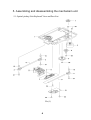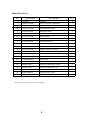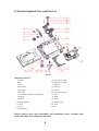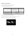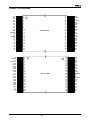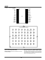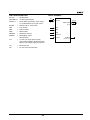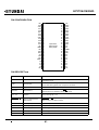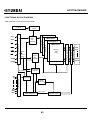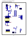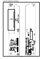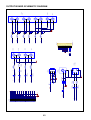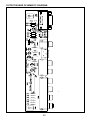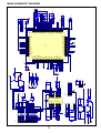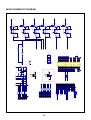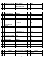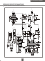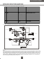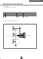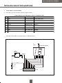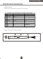
1
SERVICE MANUAL
STC-9630
1
MIC
2
OPEN/CLOSE
CONTENTS
1.
SAFETY PRECAUTIONS
2.
PREVENTION OF ELECTRO STATIC DISCHARGE(ESD)TO ELECTROSTATICALLY
1
SENSITIVE(ES)DEVICES
1
3.
CONTROL BUTTON LOCATIONS AND EXPLANATIONS
2
4.
PREVERTION OF STATIC ELECTRICITY DISCHARGE
3
5.
ASSEMBLING AND DISASSEMBLING THE MECHANISM UNIT
4
5.1
OPTICAL PICKUP UNIT EXPLOSED VIEW AND PART LIST
4
5.2
BRACKET EXPLOSED VIEW AND PART LIST
6
5.3
MISCELLANEOUS
7
6.
ELECTRICAL CONFIRMATION
8
6.1
VIDEO OUTPUT (LUMINANCE SIGNAL) CONFIRMATION
8
6.2
VIDEO OUTPUT(CHROMINANCE SIGNAL) CONFIRMATION
9
7.
MPEG BOARD CHECK WAVEFORM
10
8.
IC BLOCK DIAGRAM & DESCRIPTION
11
8.1
MT1336
11
8.2
MT1379
19
8.3
AM29LV160D
35
8.4
HY57V641620HG
40
9.
10.
SCHEMATIC & PCB WIRING DIAGRAM
SPARE PARTS LIST
43
56
1. SAFETY PREAUTIONS
1.1 GENERAL GUIDELINES
1. When servicing, observe the original lead dress. if a short circuit is found, replace all parts which have
been overheated or damaged by the short circuit.
2. After servicing, see to it that all the protective devices such as insulation barrier, insulation papers
shields are properly installed.
3. After servicing, make the following leakage current checks to prevent the customer from being exposed
to shock hazards.
2.PREVENTION OF ELECTRO STATIC DISCHARGE(ESD)TO
ELECTROSTATICALLY SENSITIVE(ES)DEVICES
Some semiconductor(solid state)devices can be damaged easily by static electricity. Such components
commonly are called Electrostatically Sensitive(ES)Devices. Examples of typical ES devices are integrated
circuits and some field-effect transistors and semiconductor chip components. The following techniques
should be used to help reduce the incidence of component damage caused by electro static discharge(ESD).
1. Immediately before handling any semiconductor component or semiconductor-equipped assembly, drain
off any ESD on your body by touching a known earth ground. Alternatively, obtain and wear a commercially
availabel discharging ESD wrist strap, which should be removed for potential shock reasons prior to
applying power to the unit under test.
2. After removing an electrical assembly equipped with ES devices,place the assembly on a conductive
surface such as alminum foil, to prevent electrostatic charge buildup or exposure of the assembly.
3. Use only a grounded-tip soldering iron to solder or unsolder ES devices.
4. Use only an anti-static solder removal device. Some solder removal devices not classified as anti-static
(ESD protected)can generate electrical charge sufficient to damage ES devices.
5. Do not use freon-propelled chemicals. These can generate electrical charges sufficient to damage ES
devices.
6. Do not remove a replacement ES device from its protective package until immediately before you are
ready to install it. (Most replacement ES devices are packaged with leads electrically shorted together by
conductive foam, alminum foil or comparable conductive material).
7. Immediately before removing the protective material from the leads of a replacement ES device, touch
the protective material to the chassis or circuit assembly into which the device will be installed.
Caution
Be sure no power is applied to the chassis or circuit, and observe all other safety precautions.
8. Minimize bodily motions when handling unpackaged replacement ES devices. (Otherwise harmless motion
such as the brushing together of your clothes fabric or the lifting of your foot from a carpeted floor can
generate static electricity(ESD).
notice (1885x323x2 tiff)
1
2
1
9
10
4
5
6
7
8
OPEN/CLOSE
2
MIC
3
11
12
13
14
POWER switch
6
STOP button
11
MIC 1 VOLUME knob
2
Disc tray
7
REW button
12
MIC 2 VOLUME knob
3
OPEN/CLOSE button
8
FWD button
13
IR SENSOR
4
PLAY button
9
MIC 1 jack
14
LED display window
5
PAUSE button
10
MIC 2 jack
2
4.PREVENTION OF STATIC ELECTRICITY DISCHARGE
The laser diode in the traverse unit (optical pickup)may brake down due to static electricity of clothes or human
body. Use due caution to electrostatic breakdown when servicing and handling the laser diode.
4.1.Grounding for electrostatic breakdown prevention
Some devices such as the DVD player use the optical pickup(laser diode)and the optical pickup will be damaged
by static electricity in the working environment.Proceed servicing works under the working environment where
grounding works is completed.
4.1.1. Worktable grounding
1. Put a conductive material(sheet)or iron sheet on the area where the optical pickup is placed,and ground the
sheet.
4.1.2.Human body grounding
1 Use the anti-static wrist strap to discharge the static electricity from your body.
safety_3 (1577x409x2 tiff)
4.1.3.Handling of optical pickup
1. To keep the good quality of the optical pickup maintenance parts during transportation and before
installation, the both ends of the laser diode are short-circuited.After replacing the parts with new ones,
remove the short circuit according to the correct procedure. (See this Technical Guide).
2. Do not use a tester to check the laser diode for the optical pickup .Failure to do so willdamage the laser
diode due to the power supply in the tester.
4.2. Handling precautions for Traverse Unit (Optical Pickup)
1. Do not give a considerable shock to the traverse unit(optical pickup)as it has an extremely high-precise
structure.
2. When replacing the optical pickup, install the flexible cable and cut is short land with a nipper. See the
optical pickup replacement procedure in this Technical Guide. Before replacing the traverse unit, remove
the short pin for preventingstatic electricity and install a new unit.Connect the connector as short times as
possible.
3. The flexible cable may be cut off if an excessive force is applied to it.Use caution when handling the cable.
4. The half-fixed resistor for laser power adjustment cannot be adjusted. Do not turn the resistor.
3
5. Assembling and disassembling the mechanism unit
5.1 Optical pickup Unit Explosed View and Part List
Pic (1)
4
Materials to Pic (1)
No.
PARTS CODE
PARTS NAME
Q ty
14692200
SF-HD60
1
1
1EA0311A06300
ASSY, CHASSIS, COMPLETE
1
2
1EA0M10A15500
ASSY, MOTOR, SLED
1
Or
1EA0M10A15501
ASSY, MOTOR, SLED
1
3
1EA2451A24700
HOLDER, SHAFT
3
4
1EA2511A29100
GEAR, RACK
1
5
1EA2511A29200
GEAR, DRIVE
1
6
1EA2511A29300
GEAR, MIDDLE, A
1
7
1EA2511A29400
GEAR, MIDDLE, B
1
8
1EA2744A03000
SHAFT, SLIDE
1
9
1EA2744A03100
SHAFT, SLIDE, SUB
1
10
1EA2812A15300
SPRING, COMP, TYOUSEI
3
11
1EA2812A15400
SPRING, COMP, RACK
1
21
1EA0B10B20100
ASSY, PWB
1
Or
1EA0B10B20200
ASSY, PWB
1
31
SEXEA25700---
SPECIAL SCREW BIN+-M2X11
3
32
SEXEA25900---
SPECIAL SCREW M1.7X2.2
2
33
SFBPN204R0SE-
SCR S-TPG PAN 2X4
2
34
SFSFN266R0SE-
SCR S-TPG FLT 2.6X6
1
35
SWXEA15400---
SPECIAL WASHER 1.8X4 X0.25
2
Note : This parts list is not for service parts supply.
5
5.2 Bracket Explosed View and Part List
Pic (2)
Materials to Pic(2)
1.bracket
2.belt
3.screw
4.belt wheel
5.gearwheel
6.iron chip
7. Immobility mechanism equipment
8. Magnet
9. Platen
10. Bridge bracket
11. screw
12. screw
13. Big bracket
14. front silicon rubber
15. Back silicon rubber
16. Pick-up
17. Pick-up
18. switch
19. Five-pin flat plug
20. screw
21. PCB
22. motor
23. Motor wheel
24. screw
25.tray
Before going process with disassembly and installation, please carefully both
peruse the chart and confirm the materials.
6
5.3 MISCELLANEOUS
5.3.1 Protection of the LD(Laser diode)
Short the parts of LD circuit pattern by soldering.
5.3.2 Cautions on assembly and adjustment
Make sure that the workbenches,jigs,tips,tips of soldering irons and measuring instruments are
grounded,and that personnel wear wrist straps for ground.
Open the LD short lands quickly with a soldering iron after a circuit is connected.
Keep the power source of the pick-up protected from internal and external sources of electrical
noise.
Refrain from operation and storage in atmospheres containing corrosive gases (such as H2S,SO2,
NO2 and Cl2)or toxic gases or in locations containing substances(especially from the organic silicon,cyan,
formalin and phenol groups)which emit toxic gases.It is particularly important to ensure that none of the
above substances are present inside the unit.Otherwise,the motor may no longer run.
7
6.Electrical Confirmation
6.1. Video Output (Luminance Signal) Confirmation
DO this confirmation after replacing a P.C.B.
Measurement point
Mode
Disc
Video output terminal
Color bar 75%
PLAY(Title 46):DVDT-S15
PLAY(Title 12):DVDT-S01
DVDT-S15
or
DVDT-S01
Measuring equipment,tools
Confirmation value
200mV/dir,10 sec/dir
1000mVp-p±30mV
Purpose:To maintain video signal output compatibility.
1.Connect the oscilloscope to the video output terminal and terminate at 75 ohms.
2.Confirm that luminance signal(Y+S)level is 1000mVp-p±30mV
8
6.2 Video Output(Chrominance Signal) Confirmation
Do the confirmation after replacing P.C.B.
Measurement point
Mode
Disc
Video output terminal
Color bar 75%
PLAY(Title 46):DVDT-S15
PLAY(Title 12):DVDT-S01
DVDT-S15
or
DVDT-S01
Measuring equipment,tools
Screwdriver,Oscilloscope
200mV/dir,10 sec/dir
Confirmation value
621mVp-p±30mV
Purpose:To maintain video signal output compatibility.
1.Connect the oscilloscope to the video output terminal and terminate at 75 ohme.
2.Confirm that the chrominance signal(C)level is 621 mVp-p±30mV
9
7.MPEG BOARD CHECK WAVEFORM
7.1 27MHz WAVEFORM
DIAGRAM
7.2 IC5L0380R PIN.2 WAVEFORM DIAGRAM
10
MT1336
PRELIMINARY, SUBJ ECT TO CHANGE WITHOUT NOTICE
MTK CONFIDENTIAL, NO DISCLOSURE
8. IC BLOCK DIAGRAM & DESCRIPTION
8.1 MT1336
GENERAL DESCRIPTION
M T 1 3 3 6 i s a h i g h p e r f o r m a n c e C M O S a n a l o g f r o n t -e n d I C f o r b o t h C D _ R O M d r i v e r u p t o 4 8 X S a n d
D V D - R O M d r i v e r u p t o 1 6 X S . I t a l s o s u p p o r t s D V D- R A M r e a d u p t o 4 X S V e r s i o n 2 . I t c o n t a i n s s e r v o a m p li f i e r s
t o g e n e r a t e f o c u s i n g e r r o r , 3-b e a m t r a c k i n g e r r o r , 1 b e a m r a d i a l p u s h -p u l l s i g n a l , R F l e v e l a n d S B A D f o r s e r v o
f u n c t i o n s . I t a l s o i n c l u d e s D P D t r a c k i n g e r r o r s i g n a l f o r D V D _ R O M a p p l i c a t i o n . F o r D V D- R A M d i s k s , t h e r e a r e
a l s o D i f f e r e n t i a l P u s h -P u l l ( D P P ) m e t h o d f o r g e n e r a t i n g t r a c k i n g s i g n a l a n d D i f f e r e n t i a l A s t i g m a t i c D e t e c t i o n
(DAD) for processing focusing signal. Programmable equalizer and AGC circuits are also incorporated in this
chip to optimize read channel performance. In addition, this chip has dual automatic laser power control circuits
f o r D V D- R O M ( D V D-R A M )
and
C D -R O M s e p e r a t e l y a n d r e f e r e n c e v o l t a g e g e n e r a t o r s t o r e d u c e e x t e r n a l
c o m p o n e n t s . P r o g r a m m a b l e f u n c t i o n s a r e i m p l e m e n t e d b y t h e a c c e s s o f i n t e r n a l r e g i s t e r t h r o u g h b i -d i r e c t i o n a l
serial port to configure modes selection.
FEATURES
n
RF equalizer with programmable
fc
from 3MHz to 70 MHz and programmable boost from 3dB to
13dB.
n
M T 1 3 3 6 s u p p o r t s a t l e a s t e i g h t d i f f e r e n t k i n d s o f p i c k-u p h e a d s w i t h v e r s a t i l e i n p u t c o n f i g u r a t i o n f o r
both RF input stages and servo signal blocks.
n
Versatile on -line AGC.
n
3 beams tracking error signal generator for CD_ROM application.
n
One beam differential phase tracking error (DPD) generator for DVD_ROM application.
n
Differential push pull tracki ng error (DPP) generator for DVD_RAM application.
n
Focusing error signal generator for CD-ROM, DVD-ROM and DVD-RAM (DAD method).
n
RF level signal generator.
n
Sub-beam added signal for 3 beams CD_ROM.
n
One beam push -pull signal generator for central servo application.
n
High speed RF envelop detection circuit with bandwidth up to 400KHz for CD-ROM.
n
Defect and Blank detection circuits.
n
Dual automatic laser power control circuits with programmable level of LD monitor voltage.
n
Vref=1.4V voltage and V2ref=2.8V voltage generators.
n
V20=2.0V voltage for pick -up head reference.
n
Bi-directional serial port to access internal registers.
11
MT1336
PRELIMINARY, SUBJ ECT TO CHANGE WITHOUT NOTICE
MTK CONFIDENTIAL, NO DISCLOSURE
OSP
DVDA
OSN
CDA
DVDB
RFOP
ATTENUATOR
INPUT MUX
VGA
EQ
RFON
CDB
DVDC
LRFRP
CDC
DEFECT
DVDD
HRFRP
CDD
DVDRFIN
CRTP
ENVELOP
CRTPLP
DETECTOR
DVDRFIP
AGC
MA
CSO
MB
MC
LVL
MD
DPD
SA
TEO
SB
FEO
SC
REFCOS
SD
SBAD
PCS
HALLCOS
COSPHI
DPFN
REFSIN
DPFO
HALLSIN
IR
SINPHI
DPDMUTE
TE
DVD
MDI2
APC
TPI
TNI
LDO2
CDFOP
RF
CDFON
LEVEL
RFGC
RFGCU
MDI1
CD
FE
RFGCI
APC
AGC1
LDO1
AGC2
CENTRAL
AGC3
SERVO
RFSUBO
WOBSO
UDGATE
IDGATE
WOBBLE
VFO13
DET
SDATA
SERIAL
V20
V2REFO
REF and 2VREF
PORT
Voltage Generator
VREFO
MT1336 FUNCTION BLOCKS DIAGRAM
12
SLCK
SDEN
MT1336
CDFOP
SD
SC
AVDD
IR
AGND
SB
SA
MD
MC
TNI
TPI
SVDD
CDFON
WAGND
SGND
WAVDD
AGC1
MDI2
AGC3
AGC2
LDO2
LDO1
MDI1
MTK CONFIDENTIAL, NO DISCLOSURE
128
127
126
125
124
123
122
121
120
119
118
117
116
115
114
113
112
111
110
109
108
107
106
105
104
103
WGND
RFSUBO
PRELIMINARY, SUBJ ECT TO CHANGE WITHOUT NOTICE
MT1336
DVD-ROM
With
DVD_RAM
Read
MT1336 PIN ASSIGNMENT
13
AGNDP
AGNDX
AVDDP
AVDDT
V2REFO
VREFO
V20
FEO
LVL
CSO
TEO
VDDP
DEFECT
LRFRP
HRFRP
CRTP
CRTPLP
TRLPA
TRLP
HTRC
GNDP
DPFN
DPFO
AGNDX
AGNDX
AGNDX
VDD
VFO13
12
13
14
15
16
17
18
19
20
21
22
23
24
25
26
27
28
29
30
31
32
33
34
35
36
37
38
DPDMUTE
AGNDT
TM4
GNDS
SDEN
SDATA
RST
TM1
TM2
TM3
39
40
41
42
43
44
45
46
47
48
49
50
51
52
53
54
55
56
57
58
59
60
61
62
63
64
RFOP
RFON
AGNDO
1
2
3
4
5
6
7
8
9
10
11
GND
UDGATE
HDGATE
IO0
IO1
IO2
IO3
IO4
IO5
IO6
IO7
IO8
IO9
IOA
IOB
VDDS
XCK16M
SCLK
WOBSO
WVDD
AGNDX
AGNDX
AVDDO
102
101
100
99
98
97
96
95
94
93
92
91
90
89
88
87
86
85
84
83
82
81
80
79
78
77
76
75
74
73
72
71
70
69
68
67
66
65
MB
MA
DVDA
DVDB
DVDC
DVDD
DVDRFIP
DVDRFIN
CDA
CDB
CDC
CDD
OSN
OSP
RFGC
RFGCU
RFGCI
CEQP
CEQN
AGNDX
AGNDX
MON
MOP
SW1
SW2
SWO
SINPHI
REFSIN
HALLSIN
AGNDM
REFCOS
HALLCOS
COSPHI
AVDDM
AGNDX
AVDDF
VCON
AGNDF
MT1336
PRELIMINARY, SUBJ ECT TO CHANGE WITHOUT NOTICE
MTK CONFIDENTIAL, NO DISCLOSURE
MT1336 PIN DESCRIPTIONS
Pin Numbers
Symbol
Type
Description
DEFECT
Digital Output
56
SCLK
Digital Input
RF serial clock input
58
SDEN
Digital Input
RF serial data enable
59
SDATA
Digital IO
60
RST
Digital input
Reset (active high)
55
XCK16M
Digital Input
16.9MHz for verification
LQFP128
RF Flag Interface
23
Flag of bad data output status
RF SIO interface
RF serial data IO
RF SERVO interface
40
UDGATE
Digital Input
Con trol signal for DVD-RAM
41
IDGATE
Digital Input
Control signal for DVD -RAM
38
VFO13
Digital Input
DVD -RAM Header signal
RF
100
DVDA
Analog input
AC coupled DVD RF signal input A
99
DVDB
Analog Input
AC coupled DVD RF signal input
98
DVDC
Analog Input
AC coupled DVD RF signal input C
97
DVDD
Analog Input
AC coupled DVD RF signal input D
95
DVDRFIN
Analog Input
AC coupled DVD RF signal input RFIN
96
DVDRFIP
Analog Input
AC coupled DVD RF signal input RFIP
94
CDA
Analog Input
AC coupled CD RF signal input A
93
CDB
Analog Input
AC coupled CD RF signal input B
92
CDC
Analog Input
AC coupled CD RF signal input C
91
CDD
Analog Input
AC coupled CD RF signal input D
90
OSN
Analog
RF Offset cancellation capacitor connecting
89
OSP
Analog
RF Offset cancellation capacitor connecting
85
CEQP
Analog
RF Offset cancellation capacitor connecting
84
CEQN
Analog
RF Offset cancellation capacitor connecting
88
RFGC
Analog
RF AGC loop capacitor connecting for DVD -ROM
14
B
MT1336
PRELIMINARY, SUBJ ECT TO CHANGE WITHOUT NOTICE
MTK CONFIDENTIAL, NO DISCLOSURE
87
RFGCU
Analog
RF AGC loop capacitor connecting for DVD -RAM
86
RFGCI
Analog
RF AGC loop capacitor connecting for DVD -RAM
101
MA
Analog Input
DC coupled DVD-RAM main-beam RF signal input A
102
MB
Analog Input
DC coupled DVD-RAM main-beam RF signal input B
103
MC
Analog Input
DC coupled DVD-RAM main-beam RF signal input C
104
MD
Analog Input
DC coupled DVD-RAM main-beam RF signal input D
105
SA
Analog Input
DC coupled DVD-RAM sub-beam RF signal input A
106
SB
Analog Input
DC coupled DVD-RAM sub-beam RF signal input B
110
SC
Analog Input
DC coupled DVD-RAM sub-beam RF signal input C
111
SD
Analog Input
DC coupled DVD-RAM sub-beam RF signal input D
108
IR
Analog
External current bias resistor (R=20K)
119
AGC1
Analog
Wobble AGC loop1 capacitor
121
AGC2
Analog
Wobble AGC loop2 capacitor
122
AGC3
Analog
Wobble AGC loop3 capacitor
127
RFSUBO
Analog output
Header push-pull RF output signal
1
WOBSO
Digital output
Wobble signal output
6
RFOP
Analog output
RF positive output
7
RFON
Analog output
RF negative output
32
DPFN
Analog
DPD amplifier negative input
33
DPFO
Analog
DPD amplifier output
61
DPDMUTE
Digital input
DPD mute control input
116
TNI
Analog Input
3 beam satellite PD signal negative input
115
TPI
Analog Input
3 beam satellite PD signal positive input
21
TEO
Analog Output
TRACKING ERROR
FOCUSING ERROR & RF LEVEL
Tracking error output
& CENTRAL SERVO SIGNAL
112
CDFOP
Analog Input
CD focusing error positive input
113
CDFON
Analog Input
CD focusing error negative input
18
FEO
Analog Output
Focusing error output
19
LVL
Analog Output
RF level output
20
CSO
Analog output
Central servo signal output
ALPC
15
MT1336
PRELIMINARY, SUBJ ECT TO CHANGE WITHOUT NOTICE
MTK CONFIDENTIAL, NO DISCLOSURE
124
MDI1
Analog Input
125
LDO1
Analog Ou tput
123
MDI2
Analog Input
126
LDO2
Analog Output
26
CRTP
Analog
RF top envelop filter capacitor connecting
27
CRTPLP
Analog
Defect level filter capacitor connecting
25
HRFRP
Analog output
High frequency RF ripple output or Blank detector’s output
24
LRFRP
Analog output
Low frequency RF ripple output
67, 69
AVDD
Power
65, 73
AGND
GND
64
AVDD
Power
DPD Power
62
AGND
GND
DPD GND
109
AVDD
Power
107
AGND
GND
RF path GND
114
SVDD
Power
Servo Power
117
SGND
GND
2,120
WAVDD
Power
128,118
WAGND
GND
5
AVDDO
Power
Power for RF output
8
AGNDO
GND
GND for RF output
14
AVDDT
Power
12
AGNDT
GND
GND for Trimming PAD
22
VDDP
Power
Peak Detection Power
31
GNDP
GND
Peak Detection GND
37,54
VDD
Power
Serial I/O Power
39,57
GND
GND
Serial I/O GND
Laser power monitor input
Laser driver output
Laser power monitor input
Laser driver output
RF RIPPLE
POWER
Master PLL Filter power
GND for Master PLL Filter
RF path Power
Servo GND
Wobble Power
Wobble GND
Power for Trimming PAD
REFERENCE VOLTAGE
16
VREFO
Analog output
Reference voltage 1.4V
15
V2REFO
Analog output
Reference voltage 2.8V
17
V20
Analog Output
Reference voltage 2.0V
16
MT1336
PRELIMINARY, SUBJ ECT TO CHANGE WITHOUT NOTICE
MTK CONFIDENTIAL, NO DISCLOSURE
ALPC TRIMMING
9
TM1
Analog input
Trimming pin for ALPC1
10
TM2
Analog input
Trimming pin for ALPC1
11
TM3
Analog input
Trimming pin for ALPC2
13
TM4
Analog input
Trimming pin for ALPC2
HIGH SPEED TRACK COUNTING
29
TRLP
Analog
Low-pass filter capacitor connecting
28
TRLPA
Analog
Low-pass filter capacitor connecting
30
HTRC
Digital output
High speed track counting digital output
74
HALLSIN
Analog input
Negative input of amplifier for hall sensor signal
75
REFSIN
Analog input
Positive input of amplifier for hall sensor signal
76
SINPHI
Analog output
Amplifier output for hall sensor signal
71
HALLCOS
Analog input
Negative input of amplifier for hall sensor signal
72
REFCOS
Analog input
Positive input of amplifier for hall sensor signal
70
COSPHI
Analog output
Amplifier output for hall sensor signal
PCS
FOR MONITOR ONLY
81
MON
Analog output
80
MOP
Analog output
66
VCON
Analog output
77
SWO
Analog output
Output from mux of SW1 & SW2
78
SW2
Analog input
External input for servo input select
79
SW1
Analog input
External input for servo input select
FOR SERIAL I/O
42
IO0
43
IO1
44
IO2
45
IO3
46
IO4
47
IO5
17
MT1336
PRELIMINARY, SUBJ ECT TO CHANGE WITHOUT NOTICE
48
IO6
49
IO7
50
IO8
51
IO9
52
IOA
53
IOB
MTK CONFIDENTIAL, NO DISCLOSURE
18
MT1379
Progressive Scan DVD Player Combo Chip
Specificationsaresubjecttochangewithoutnotice
8.2 MT1379
n Super Integration DVD player single chip
§
Servo controller and data channel processing
§
MPEG-1/MPEG-2/JPEG video decoding
Dolby AC-3/DTS/DVD -Audio audio decoding
§
§
§
§
§
§
Built-in TV encoder
Built-in progressive video output
§
Video input port and audio/SPDIF input port
§
§
§
§
§
§
Built-in DSP for digital servo control
§
Built-in 8032 micro controller
§
Built-in internal 373 and 8-bit programmable
lower address port
§
1024-bytes on-chip RAM
Up to 2M bytes FLASH-programming interface
Supports 5/3.3-Volt. FLASH interface
§
§
§
§
Built-in a frequency programmable clock to µP
and RSPC Decoder to optimize the performance
over power
§
§
§
Provides interface with analog front-end
processor
Analog data slicer for small jitter capability
§
§
Built-in high performance data PLL for chann el
data demodulation
§
EFM/EFM+ data demodulation
Enhanced channel data frame sync protection &
DVD-ROM sector sync protection
§
§
§
n Servo Control and Spindle Motor Control
§
§
Programmable frequency error gain and phase
error gain of spindle PLL to control spindle motor
on CLV and CAV mode
Provide a varipitch speed control for CLV and CAV
mode
Built-in ADCs and DACs for digital servo control
§
Provide 2 general PWM
§
Supports power-down mode
Supports additional serial port
n DVD-ROM/CD-ROM Decoding Logic
DVD-ROM up to 8XS
CD-ROM up to 24XS
n Channel Data Processor
§
§
§
n Speed Performance on Servo and Decoding
§
Tray control can be PWM output or digital output
n Host Micro controller
Unified track buffer and A/V decoding buffer
Video processing for scaling and video quality
enhancement
OSD & Sub-picture decoding
Built-in clock generator
§
§
19
Supports CD-ROM Mode 1, CD-ROM XA Mode 2
Form 1, CD-ROM XA Mode 2 Form 2, and CD-DA
formats
High-speed ECC logic capable of correcting one
error per each P-codeword or Q-codeword
Automatic sector Mode and Form detection
Automatic sector Header verification
8-bit counter for decode completion check
Programmable descrambling and error
correction schemes
Automatically repeated error corrections
8-bit C2 Pointer counter
Decoder Error Notification Interrupt that signals
various decoder errors
Provide error correction acceleration
n Buffer Memory Controller
§
Supports 16Mb/32Mb/64Mb/128Mb SDRAM
§
§
Supports 16-bit/32-bit SDRAM data bus interface
Build in a DRAM interface programmable clock to
optimize the DRAM performance
Provide the self-refresh mode SDRAM
§
Programmable DRAM access cycle and refresh
§
MT1379
PRELIMINARY, SUBJECT TO CHANGE WITHOUT NOTICE
§
MTK CONFIDENTIAL, NO DISCLOSURE
§
cycle timings
Block-based sector addressing
§
§
Programmable buffering counter for buffer status
tracking
§
Maximum DRAM speed is 133MHz
Support 5/3.3-Volt. DRAM Interface
§
§
§
n Video Decode
§
§
Decodes MPEG1 video and MPEG2 main level,
main profile video (720/480 and 720x576)
Maximum input bit-rate of 15Mbits/sec
§
Smooth digest view function with I, P and B
picture decoding
§
Baseline, extended-sequential and progressive
JPEG image decoding
§
RLE and non-RLE BMP image decoding
Support CD-G titles
§
§
§
§
§
§
§
§
§
§
§
HDCD certified
§
§
Six 54MHz/12bit DA converters
Support NTSC, PAL-BDGHI, PAL-N, PAL-M
interlace TV format and 480p, 576p progressive
TV format
Automatically turn off unconnected channel(s).
Support PC monitor (VGA)
§
Support Macrovision 7.1
§
256/16 color RLC format OSD
Automatic scrolling of OSD image
§
Provides 4 -color/32x32-pixel hardware cursor
Fade-in, Fade out, and Wipe functions as
specified in the DVD-Audio Specification and
other slide show transition effects
Progressive scan output
n Progressive Output
§
Automatic detect film or video source
§
3:2 pull down source detection
Advanced Motion adaptive de-interlace
Minimum external memory requirement
§
Decoder format supports:
- Dolby Digital (AC -3) decoding
§
- DTS decoding
- MLP decoding for DVD -Audio
n Audio/Video Output
§
- MPEG-1 layer 1/layer 2 audio decoding
- MPEG-2 layer1/layer2 2 -channel audio decoding
- Dolby Pro Logic decoding
- High Definition Compatible Digital (HDCD)
decoding
§
Karaoke functions
- Microphone echo with adjustable echo level,
echo -depth and delay length
- Microphone tone control with three custom
second-order IIR filter
- Vocal mute/vocal assistant
- Key shift up to +/- 8 keys controlled by 1/2 key
n TV Encoder
Arbitrary ratio vertical/horizontal scaling of video,
from 0.25X to 256X
65535/256/16/4/2-color bitmap format OSD,
n Audio Processing
§
- PCM / bit stream / mute mode
- Custom IEC latency up to 2 frames
Pink noise and white noise generator
Channel equalizer
3D surround processing include virtual surround
and speaker separation
Power-down control
§
n Video/OSD/SPU/HLI Processor
Downmix function
Support IEC 60958/61937 output
§
§
Line-in/SPDIF-in for versatile audio processing
CCIR601/656 video input port
Support picture-in-picture for video decoding and
input source
n Outline
Up to 6 channel linear PCM output for DVD Audio
/ DVD Video
20
§
§
216-pin LQFP package
3.3/2.5-Volt. Dual operating voltages
MT1379
PRELIMINARY, SUBJECT TO CHANGE WITHOUT NOTICE
MTK CONFIDENTIAL, NO DISCLOSURE
P IN D EFINITIONS
Pin Number
Symbol
Type
1
IREF
Analog Input
2
3
4
5
6
7
8
9
10
11
12
13
14
PLLVSS
LPIOP
LPION
LPFON
LPFIP
LPFIN
LPFOP
JITFO
JITFN
PLLVDD3
FOO
TRO
TROPENPWM
Ground
Analog Output
Analog Output
Analog output
Analog Input
Analog Input
Analog Output
Analog Output
Analog Input
Power
Analog Output
Analog Output
Analog Output
15
16
17
18
19
20
21
22
PWMOUT1
PWMOUT2
DVDD2
DMO
FMO
DVSS
FG
HIGHA0
23
HIGHA1
24
HIGHA2
25
HIGHA3
26
HIGHA4
27
HIGHA5
28
DVSS
Analog Output
Analog Output
Power
Analog Output
Analog Output
Ground
Input
Inout
2~16MA, SR
PU
Inout
2~16MA, SR
PU
Inout
2~16MA, SR
PU
Inout
2~16MA, SR
PU
Inout
2~16MA, SR
PU
Inout
2~16MA, SR
PU
Grou nd
Description
Current reference input. It generates reference current for data
PLL.
Connect an ext ernal 100K resistor to this pin and PLLVSS.
Ground pin for data PLL and related analog circuitry
Positive output of the low pass filter
Negative output of the low pass filter
Negative output of loop filter amplifier
Positive input of loop filter amplifier
Negative input of loop filter amplifier
Positive output of loop filter amplifier
RF jitter meter output
Negative input of the operation amplifier for RF jigger meter
3.3V power pin for data PLL and related analog circuitry
Focus servo output. PDM output of focus servo compensator
Tracking servo output. PDM output of tracking servo compensator
Tray open output, controlled by microcontroller.
This is PWM output for TRWMEN27hRW2=1 or is digital output for
TRWMEN27hRW2=0
The 1st general PWM output
The 2nd general PWM output
2.5V power pin for internal fully digital circuitry
Disk motor control output. PWM output
Feed motor control. PWM output
Ground pin for internal fully digital circuitry
Motor Hall sensor input
Microcontroller address 8
Microcontroller address 9
Microcontroller address 10
Microcontroller address 11
Microcontroller address 12
Microcontroller address 13
Ground pin for internal digital circuitry
21
MT1379
PRELIMINARY, SUBJECT TO CHANGE WITHOUT NOTICE
MTK CONFIDENTIAL, NO DISCLOSURE
Pin Number
Symbol
Type
29
HIGHA6
30
HIGHA7
31
AD7
32
AD6
33
AD5
34
AD4
35
36
DVDD3
AD3
37
AD2
38
AD1
39
AD0
40
IOA0
41
IOA1
42
43
DVDD2
IOA2
44
IOA3
45
IOA4
46
IOA5
47
IOA6
Inout
2~16MA, SR
PU
Inout
2~16MA, SR
PU
Inout
2~16MA, SR
Inout
2~16MA, SR
Inout
2~16MA, SR
Inout
2~16MA, SR
Power
Inout
2~16MA, SR
Inout
2~16MA, SR
Inout
2~16MA, SR
Inout
2~16MA, SR
Inout
2~16MA, SR
PU
Inout
2~16MA, SR
PU
Power
Inout
2~16MA, SR
PU
Inout
2~16MA, SR
PU
Inout
2~16MA, SR
PU
Inout
2~16MA, SR
PU
Inout
2~16MA, SR
PU
Description
Microcontroller address 14
Microcontroller address 15
Microcontroller address/data 7
Microcontroller address/data 6
Microcontroller address/data 5
Microcontroller address/data 4
3.3V power pin for internal digital circuitry
Microcontroller address/data 3
Microcontroller address/data 2
Microcontroller address/data 1
Microcontroller address/data 0
Microcontroller address 0 / IO
Microcontroller address 1 / IO
2.5V power pin for internal digital circuitry
Microcontroller address 2 / IO
Microcontroller address 3 / IO
Microcontroller address 4 / IO
Microcontroller address 5 / IO
Microcontroller address 6 / IO
22
MT1379
PRELIMINARY, SUBJECT TO CHANGE WITHOUT NOTICE
MTK CONFIDENTIAL, NO DISCLOSURE
Pin Number
Symbol
Type
48
IOA7
49
A16
50
A17
51
IOA18
52
IOA19
53
IOA20
54
55
56
APLLVSS
APLLVDD3
ALE
57
IOOE#
58
IOWR#
59
IOCS#
60
61
DVSS
UP1_2
62
UP1_3
63
UP1_4
64
UP1_5
65
UP1_6
66
DVDD3
Inout
2~16MA, SR
PU
Output
2~16MA, SR
Output
2~16MA, SR
Inout
2~16MA, SR
SMT
Inout
2~16MA, SR
SMT
Inout
2~16MA, SR
SMT
Ground
Power
Inout
2~16MA, SR
PU, SMT
Inout
2~16MA, SR
SMT
Inout
2~16MA, SR
SMT
Inout
2~16MA, SR
PU, SMT
Ground
Inout
4MA, SR
PU, SMT
Inout
4MA, SR
PU, SMT
Inout
4MA, SR
PU, SMT
Inout
4MA, SR
PU, SMT
Inout
4MA, SR
PU, SMT
Power
Description
Microcontroller address 7 / IO
Flash address 16
Flash address 17
Flash address 18 / IO
Flash address 19 / IO
Flash address 20 / IO
OR Videoin Data PortB 0
Ground pin for audio clock circuitry
3.3V Power pin for audio clock circuitry
Microcontroller address latch enable
Flash output enable, active low / IO
Flash write enable, active low / IO
Flash chip select, active low / IO
Ground pin for internal digital circuitry
Microcontroller port 1 -2
Microcontroller port 1 -3
Microcontroller port 1 -4
Microcontroller port 1 -5
Microcontroller port 1 -6
3.3V power pin for internal digital circuitry
23
MT1379
PRELIMINARY, SUBJECT TO CHANGE WITHOUT NOTICE
MTK CONFIDENTIAL, NO DISCLOSURE
Pin Number
Symbol
Type
67
UP1_7
68
UP3_0
69
UP3_1
70
INT0#
71
IR
72
73
74
75
DVDD2
UP3_4
UP3_5
UWR#
76
URD#
77
78
79
80
81
82
83
84
85
86
87
DVSS
RD7
RD6
RD5
RD4
DVDD2
RD3
RD2
RD1
RD0
RWE#
88
CAS#
89
RAS#
90
RCS#
91
BA0
92
93
DVSS
RD15
Inout
4MA, SR
PU, SMT
Inout
4MA, SR
PU, SMT
Inout
4MA, SR
PU, SMT
Inout
2~16MA, SR
PU, SMT
Input
SMT
Power
Inout
Inout
Inout
2~16MA, SR
PU, SMT
Inout
2~16MA, SR
PU, SMT
Ground
Inout
Inout
Inout
Inout
Power
Inout
Inout
Inout
Inout
Output
2~16MA, SR
Output
2~16MA, SR
Output
2~16MA, SR
Output
2~16MA, SR
Output
2~16MA, SR
Ground
Inout
2~16MA, SR
PU/PD, SMT
Description
Microcontroller port 1 -7
Microcontroller port 3 -0
Microcontroller port 3 -1
Microcontroller interrupt 0, active low
IR control signal input
2.5V power pin for internal digital circuitry
Microcontroller port 3 -4
Microcontroller port 3 -5
Microcontroller write strobe, active low
Microcontroller read strobe, active low
Ground pin for internal digital circuitry
DRAM data 7
DRAM data 6
DRAM data 5
DRAM data 4
2.5V power pin for internal digital circuitry
DRAM data 3
DRAM data 2
DRAM data 1
DRAM data 0
DRAM Write enable, active low
DRAM columnaddress strobe, active low
DRAM row address strobe, active low
DRAM chip select, active low
DRAM bank address 0
Ground pin for internal digital circuitry
DRAM data 15
24
MT1379
PRELIMINARY, SUBJECT TO CHANGE WITHOUT NOTICE
MTK CONFIDENTIAL, NO DISCLOSURE
Pin Number
Symbol
Type
94
RD14
95
RD13
96
RD12
97
98
DVDD3
RD11
99
RD10
100
RD9
101
RD8
102
103
DVSS
CLK
104
CLE
105
RA11
106
RA9
107
RA8
108
109
110
DMVDD3
DMVSS
RA7
111
112
DVDD3
RA6
113
RA5
114
RA4
115
116
DVSS
DQM1
Inout
2~16MA, SR
PU/PD, SMT
Inout
2~16MA, SR
PU/PD, SMT
Inout
2~16MA, SR
PU/PD, SMT
Power
Inout
2~16MA, SR
PU/PD, SMT
Inout
2~16MA, SR
PU/PD, SMT
Inout
2~16MA, SR
PU/PD, SMT
Inout
2~16MA, SR
PU/PD, SMT
Ground
Output
2~16MA, SR
Output
2~16MA, SR
Output
2~16MA, SR
Output
2~16MA, SR
Output
2~16MA, SR
Power
Ground
Output
2~16MA, SR
Power
Output
2~16MA, SR
Output
2~16MA, SR
Output
2~16MA, SR
Ground
Output
2~16MA, SR
Description
DRAM data 14
DRAM data 13
DRAM data 12
3.3V power pin for internal digital circuitry
DRAM data 11
DRAM data 10
DRAM data 9
DRAM data 8
Ground pin for internal digital circuitry
DRAM clock
DRAM clock enable
DRAM address bit 11 or audio serial data 3 (channel 7/8)
DRAM address 9
DRAM address 8
3.3V Power pin for DRAM clock circuitry
Ground pin for DRAM clock circuitry
DRAM address 7
3.3V power pin for internal digital circuitry
DRAM address 6
DRAM address 5
DRAM address 4
Ground pin for internal digital circuitry
Mask for DRAM input/output byte 1
25
MT1379
PRELIMINARY, SUBJECT TO CHANGE WITHOUT NOTICE
MTK CONFIDENTIAL, NO DISCLOSURE
Pin Number
Symbol
Type
117
DQM0
118
BA1
119
RA10
120
121
DVDD2
RA0
122
RA1
123
RA2
124
RA3
125
126
DVSS
RD31
127
RD30
128
RD29
129
RD28
130
131
DVDD3
RD27
132
RD26
133
RD25
134
RD24
135
136
DVSS
DQM3
137
DQM2
Output
2~16MA, SR
Output
2~16MA, SR
Output
2~16MA, SR
Power
Output
2~16MA, SR
Output
2~16MA, SR
Output
2~16MA, SR
Output
2~16MA, SR
Ground
Inout
2~16MA, SR
PU/PD, SMT
Inout
2~16MA, SR
PU/PD, SMT
Inout
2~16MA, SR
PU/PD, SMT
Inout
2~16MA, SR
PU/PD, SMT
Power
Inout
2~16MA, SR
PU/PD, SMT
Inout
2~16MA, SR
PU/PD, SMT
Inout
2~16MA, SR
PU/PD, SMT
Inout
2~16MA, SR
PU/PD, SMT
Ground
Output
2~16MA, SR
Output
2~16MA, SR
Description
Mask for DRAM input/output byte 0
DRAM bank address 0
DRAM address10
2.5V power pin for internal digital circuitry
DRAM address 0
DRAM address 1
DRAM address 2
DRAM address 3
Ground pin for internal digital circuitry
DRAM data 31
DRAM data 30
DRAM data 29
DRAM data 28
3.3V power pin for internal digital circuitry
DRAM data 27
DRAM data 26
DRAM data 25
DRAM data 24
Ground pin for internal digital circuitry
Mask for DRAM input/output byte 3
Mask for DRAM input/output byte 2
26
MT1379
PRELIMINARY, SUBJECT TO CHANGE WITHOUT NOTICE
MTK CONFIDENTIAL, NO DISCLOSURE
Pin Number
Symbol
Type
138
RD23
139
RD22
140
141
DVDD2
RD21
142
RD20
143
RD19
144
RD18
145
146
DVSS
RD17
147
RD16
148
ABCK
149
ALRCK
150
151
DVDD3
ACLK
152
153
MC_DATA
SPDIF
154
ASDATA0
155
ASDATA1
156
ASDATA2
Inout
2~16MA, SR
PU/PD, SMT
Inout
2~16MA, SR
PU/PD, SMT
Power
Inout
2~16MA, SR
PU/PD, SMT
Inout
2~16MA, SR
PU/PD, SMT
Inout
2~16MA, SR
PU/PD, SMT
Inout
2~16MA, SR
PU/PD, SMT
Ground
Inout
2~16MA, SR
PU/PD, SMT
Inout
2~16MA, SR
PU/PD, SMT
Output
4MA
Inout
4MA,
PD, SMT
Power
Inout
4MA
Input
Output
2~16MA,
SR : ON/OFF
Inout
4MA
PD SMT
Inout
4MA
PD SMT
Inout
4MA
PD SMT
Description
DRAM data 23 /
Videoin Data PortA 7
DRAM data 22 /
Videoin Data PortA 6
2.5V power pin for internal digital circuitry
DRAM data 21 /
Videoin Data PortA 5
DRAM data 20 /
Videoin Data PortA 4
DRAM data 19 /
Videoin Data PortA 3
DRAM data 18 /
Videoin Data PortA 2
Ground pin for internal digital circuitry
DRAM data 17 /
Videoin Data PortA 1
DRAM data 16 /
Videoin Data PortA 0
Audio bit clock
(1) Audio left/right channel clock
(2) Trap value in power-on reset :
1 : use external 373
0: use internal 373
3.3V power pin for internal digital circuitry
Audio DAC master clock (384/256 audio sample frequency)
Microphone serial input
SPDIF output
(1)
(2)
(1)
(2)
(1)
(2)
Audio serial data 0 (left/right channel)
Trap value in power-on reset :
1 : manufactory test mode 0 : normal operation
Audio serial data 1 (surround left/surround right channel)
Trap value in power-on reset :
1 : manufactory test mode 0 : normal operation
Audio serial data 2 (center/left channel)
Trap value in power-on reset :
1 : manufactory test mode 0 : normal operation
27
MT1379
PRELIMINARY, SUBJECT TO CHANGE WITHOUT NOTICE
MTK CONFIDENTIAL, NO DISCLOSURE
Pin Number
Symbol
Type
157
ASDATA3
Inout
4MA
PD SMT
158
ASDATA4
Inout
4MA
PD SMT
159
160
161
162
DACVDDC
VREF
FS
YUV0/CIN
163
164
DACVSSC
YUV1/C
165
166
DACVDDB
YUV2/Y
Power
Analog input
Analog output
Output
4MA, SR
Ground
Output
4MA, SR
Power
Output
4MA, SR
Ground
Description
(1)
(2)
Audio serial data 3 (surround left/surround right channel)
Trap value in power-on reset :
1 : manufactory test mode 0 : normal operation
OR Videoin Data PortB 1
(1) Audio serial data 4 (center/left channel)
(2) Trap value in power-on reset :
1 : manufactory test mode 0 : normal operation
OR Videoin Data PortB 2
3.3V power pin for VIDEO DAC circuitry
Bandgap reference voltage
Full scale adjustment
Video data output bit 0 /
Compensation capacitor
Ground pin for VIDEO DAC circuitry
Video data output bit 1 /
Analog chroma output
3.3V power pin for VIDEO DAC circuitry
Video data output bit 2 /
Analog Y output
167
DACVSSB
168
YUV3/CVBS
Output
4MA, SR
Ground pin for VIDEO DAC circuitry
Video data output bit 3 /
Analog composite output
169
170
DACVDDA
YUV4/G
171
172
DACVSSA
YUV5/B
173
YUV6/R
174
ICE
3.3V power pin for VIDEO DAC circuitry
Video data output bit 4 /
Green or Y
Ground pin for VIDEO DAC circuitry
Video data output bit 5 /
Blue or CB
Video data output bit 6 /
Red or CR
Microcontroller ICE mode enable
175
BLANK#
176
VSYN
177
YUV7
178
179
DVSS
HSYN
180
SPMCLK
Power
Output
4MA, SR
Ground
Output
4MA, SR
Output
4MA, SR
Input
PD, SMT
Inout
4MA, SR
SMT
Inout
4MA, SR
SMT
Inout
4MA, SR
SMT
Ground
Inout
4MA, SR
SMT
Input
Video blank area, active low /
Videoin Field_601
Vertical sync /
Videoin Vsync_601
Video data output bit 7 /
Videoin Data PortB 3
Ground pin for internal digital circuitry
Horizontal sync /
Videoin Hsync_601
Audio DAC master clock of SPDIF input /
Videoin Data PortB 4
28
MT1379
PRELIMINARY, SUBJECT TO CHANGE WITHOUT NOTICE
MTK CONFIDENTIAL, NO DISCLOSURE
Pin Number
Symbol
Type
181
SPDATA
Input
182
183
DVDD2
SPLRCK
Power
Input
184
SPBCK
Input
185
186
187
188
DVDD3
XTALO
XTALI
PRST
189
190
191
192
193
194
195
196
197
198
199
200
201
202
203
204
205
206
207
208
209
210
211
212
213
214
215
216
DVSS
VFO13
IDGATE
DVDD3
UDGATE
WOBSI
SDATA
SDEN
SLCK
BDO
ADCVSS
ADIN
RFSUBI
TEZISLV
TEI
CSO
FEI
RFLEVEL
RFRP_DC
RFRP_AC
HRFZC
PWMVREF
PWM2VREF
ADCVDD3
RFDTSLVP
RFDTSLVN
RFIN
RFIP
Power
Output
Input
Input
PD, SMT
Ground
Output
Output
Power
Output
Input
Output
Output
Output
Input
Ground
Analog Input
Analog Input
Analog Input
Analog Input
Analog Input
Analog Input
Analog Input
A Input
Analog Input
Analog Input
A Input
A Input
Power
Analog Output
Analog Output
Analog Input
Analog Input
Description
Audio data of SPDIF input /
Videoin Data PortB 5
2.5V power pin for internal digital circuitry
Audio left/right channel clock of SPDIF input /
Videoin Data PortB 6
Audio bit clock of SPDIF input /
Videoin Data PortB 7
3.3V power pin for internal digital circuitry
Crystal output
Crystal input
Power on reset input, active high
Ground pin for internal digital circuitry
The 1st, 3rd header VFO pulse output
Header detect signal output
3.3V power pin for internal digital circuitry
DVD_RAM recording data gate signal output
Wobble signal input
RF serial data output
RF serial data latch enable
RF serial clock output
Flag of defect data input status
Ground pin for ADC circuitry
General A/D input
RF subtraction signal input terminal
Tracking error zero crossing low pass input
Tracking error input
Central servo input
Focus error input
Sub beam add input or RFRP low pass input
RF ripple detect input
RF ripple detect input (through AC coupling)
High frequency RF ripple zero crossing
A reference voltage input for PWM circuitry. A typical value of 4.0 v
A reference voltage input for PWM circuitry. A typical value of 2.0 v
3.3V power pin for ADC circuitry
Positive RF data slicer level output
Negative RF data slicer level output
Negative input of RF differential signal
Positive input of RF differential signal
29
MT1379
PRELIMINARY, SUBJECT TO CHANGE WITHOUT NOTICE
MTK CONFIDENTIAL, NO DISCLOSURE
26 Jul, 2002
216
215
214
213
212
211
210
209
208
207
206
205
204
203
202
201
200
199
198
197
196
195
194
193
192
191
190
189
188
187
186
185
184
183
182
181
180
179
178
177
176
175
174
173
172
171
170
169
168
167
166
165
164
163
RFIP
RFIN
RFDTSLVN
RFDTSLVP
ADCVDD3
PWM2VREF
PWMVREF
HRFZC
RFRP_AC
RFRP_DC
RFLEVEL
FEI
CSO
TEI
TEZISLV
RFSUBI
ADIN
ADCVSS
BDO
SLCK
SDEN
SDATA
WOBSI
UDGATE
DVDD3
IDGATE
VFO13
DVSS
PRST
XTALI
XTALO
DVDD3
SPBCK
SPLRCK
DVDD2
SPDATA
SPMCLK
HSYN
DVSS
YUV7
VSYN
BLANK
ICE
YUV6/R
YUV5/B
DACVSSA
YUV4/G
DACVDDA
YUV3/CVBS
DACVSSB
YUV2/Y
DACVDDB
YUV1/C
DACVSSC
Page 1 of 2
MT1379
(216 pins)
162
161
160
159
158
157
156
155
154
153
152
151
150
149
148
147
146
145
144
143
142
141
140
139
138
137
136
135
134
133
132
131
130
129
128
127
126
125
124
123
122
121
120
119
118
117
116
115
114
113
112
111
110
109
55
56
57
58
59
60
61
62
63
64
65
66
67
68
69
70
71
72
73
74
75
76
77
78
79
80
81
82
83
84
85
86
87
88
89
90
91
92
93
94
95
96
97
98
99
100
101
102
103
104
105
106
107
108
LPIOP
LPION
LPFON
LPFIP
LPFIN
LPFOP
JITFO
JITFN
PLLVDD3
FOO
TRO
TROPENPWM
PWMOUT1
PWMOUT2
DVDD2
DMO
FMO
DVSS
FG
HIGHA0
HIGHA1
HIGHA2
HIGHA3
HIGHA4
HIGHA5
DVSS
HIGHA6
HIGHA7
AD7
AD6
AD5
AD4
DVDD3
AD3
AD2
AD1
AD0
IOA0
IOA1
DVDD2
IOA2
IOA3
IOA4
IOA5
IOA6
IOA7
A16
A17
IOA18
IOA19
IOA20
APLLVSS
1
2
3
4
5
6
7
8
9
10
11
12
13
14
15
16
17
18
19
20
21
22
23
24
25
26
27
28
29
30
31
32
33
34
35
36
37
38
39
40
41
42
43
44
45
46
47
48
49
50
51
52
53
54
APLLVDD3
ALE
IOOE#
IOWR#
IOCS#
DVSS
UP1_2
UP1_3
UP1_4
UP1_5
UP1_6
DVDD3
UP1_7
UP3_0
UP3_1
INT0#
IR
DVDD2
UP3_4
UP3_5
UWR#
URD#
DVSS
RD7
RD6
RD5
RD4
DVDD2
RD3
RD2
RD1
RD0
RWE#
CAS#
RAS#
RCS#
BA0
DVSS
RD15
RD14
RD13
RD12
DVDD3
RD11
RD10
RD9
RD8
DVSS
CLK
CKE
RA11
RA9
RA8
DMVDD3
IREF
PLLVSS
30
YUV0/CIN
FS
VREF
DACVDDC
ASDATA4
ASDATA3
ASDATA2
ASDATA1
ASDATA0
SPDIF
MC_DATA
ACLK
DVDD3
ALRCK
ABCK
RD16
RD17
DVSS
RD18
RD19
RD20
RD21
DVDD2
RD22
RD23
DQM2
DQM3
DVSS
RD24
RD25
RD26
RD27
DVDD3
RD28
RD29
RD30
RD31
DVSS
RA3
RA2
RA1
RA0
DVDD2
RA10
BA1
DQM0
DQM1
DVSS
RA4
RA5
RA6
DVDD3
RA7
DMVSS
MT1379
PRELIMINARY, SUBJECT TO CHANGE WITHOUT NOTICE
MTK CONFIDENTIAL, NO DISCLOSURE
F UNCTIONAL B LOCK
DVD module
Servo
IO
Analog
Front end
Servo
DSP
Spindle
Controller
Debug
Port
Channel
Decode
DPU
System
Parser
CSS/
CPPM
TV encoder
Video
Decoder
Video
Output
Playback
Controller
IR/
VFD
System
Controller
DRAM
Interface
Flash
DRAM
Audio
Processor
Audio
Output
Audio DAC
SPDIF
Microphone
Input
MIC
Servo Controller
The servo control is accomplished through the servo DSP (Servo Digital Signal Processor) and its accessory I/O circuits. This servo
DSP is capable of performing complex operations an d also provides a friendly interface for the system controller. By issuing type
1 and type 2 commands from the system controller, the servo DSP can accomplish various complicated servo control functions,
such as tracking, seeking and MT1336/MT1376 chip register programming. As for the servo I/O circuits, it provides interface
between the input servo signals and the Servo DSP. It has built-in ADCs to digitize the servo control signal and DACs to provide
signals for the actuator and sledge motor. It also has a serial interface to communicate with the MT1336/MT1376 chip.
Analog Front End
The analog front end contains a data slicer circuit and a data PLL circuit. The RF analog signal from MT1336/MT1376 is
quantized by the data slicer to form the EFM/EFM+ bit st ream, from which the channel bit clock is extracted by the data PLL.The
EFM/EFM+bit stream and bit clock are then output to DPU for channel bit processing.
DPU
Data path unit (DPU) provides protection on data with lost synchronization patterns and demodulates EFM/EFM+ bit stream into
the channel raw data that will be corrected by the decoder. The synchronization protection makes data after the synchronization
pattern to be extracted even if the synchronization pattern is not found.
Spindle Controller
The spindle controller is used to control disc spindle motor. It includes a varipitch CLV clock generator, a CLV/CAV controller,
and a PWM generator. The varipitch CLV clock enerator generates a reference colck for the speed of operation. The CLV/CAV
31
MT1379
PRELIMINARY, SUBJECT TO CHANGE WITHOUT NOTICE
MTK CONFIDENTIAL, NO DISCLOSURE
controller changes the mode and speed of operation according to servo register setting. The PWM generator generates
pulse -width-modulated signal to drive disc spindle motor driver.
CSS/CPPM
The CSS/CPPM module provides functions necessary for decoding discs conforming to CSS/CPPM specification.
System Parser
The system parser is used to help the system controller to decode DVD/SVCD/VCD bitstream just after the channel decoder
performing error correction. Acting as a DMA master, it moves bitstream data from RSPC buffer to video, audio, or sub-picture
buffer according to system controller request. It also decrypts the scramble data of the CSS/CPPM sectors. Another function of
system parser is providing system controller/DSP a DRAM memory copy controller to enhance system controller/DSP performance.
Video Decoder
The primary function of MT1379 is to support MPEG1 and MPEG2 video decoding. The video decode engine comprises of
variable length decoder (VLD), inverse transformer (IT), motion compensator (MC), and block reconst ructor (BR). The video
decode engine decodes the variable length encoded symbols in MPEG bitstream and performs inverse scan, inverse
quantization, mismatch control and inverse discrete cosine transform onto the variable length decoded data. The motion
compensator fetches prediction data from reference picture buffer according to motion vectors and motion prediciton mode for P
and B pictures. Finally, the block reconstructor combines both the results of inverse transformer and motion compensator to derive
the reconstructed image macroblock and write back to picture buffer.
The video decode engine can also support JPEG and BMP file decoding by common image compression hardware kernels.
Video Output
The Video Output unit contains Video Processor, SPU, OSD, Cursor, TV encoder units, it performs
§
Reading decoded video from DRAM buffer
§
Scaling the image
§
Gamma/Brightness/Hue/Saturation adjustment and edge enhancement
§
Reading and decoding SPU and OSD data from DRAM buffer
§
Generating hardware cursor image
§
Merging the video data, SPU, OSD and cursor
Video Processor
The Video Processor unit controls the transfer of video data stored in the DRAM to an internal or external TV encoder. It uses
FIFOs to buffer outgoing luminance and chrominance data, and performs YUV420 to YUV422 conversion and arbitrary
vertical/horizontal decimation/interpolation, from 1/4x to 256x. With this arbitrary ratio scaling capability, the Video Processor
can perform arbitrary image conversion, such as PAL to NTSC, NTSC to PAL, MPEG1 to MPEG2, Letterbox, Pan-Scan
conversion or zoom in, zoom out. It is also capible of interlace to progressive conversion.
The Video Processor unit performs the following functions:
§ Requests and receives the decoded picture data from the picture buffer in external DRAM for display
§ Resample vertical data to create 4:2:2 sample format
§ Optionally performs vertical/horizontal resampling of both luminance and chrominance data
§ Performs optional Gamma correction, luminance/chrominance adjustment, and edge enhancement
The V ideo Processor unit contains two 2-tap vertical filters for luminance and chrominance . These filters are used to
interpolate and reposition luminance and chrominance line to improve picture quality. These filters are capble of generating
up to eight, unique subline value between two consecutive scan lines. The generation of lines depends on the ratio between
the height of the source image and the target image. In applications where DRAM bandwidth are critical the filters can be
configured as simple line-repeating to reduce the DRAM bandwidth required.
The Video Processor unit integrates two separate horizontal postprocessing filter, a simple 2-tap linear horizontal filter and
an 8-tap programmable filter. These filters are provided for scaling images horizontally along the scan line. These two filters
is capable of generating up to eight, unique subpixel values between two consecutive pixels on a scan line. The generation
of pixels depends on the ratio between the width of the source image and the target image.
SPU
32
MT1379
PRELIMINARY, SUBJECT TO CHANGE WITHOUT NOTICE
MTK CONFIDENTIAL, NO DISCLOSURE
This is a hardware sub-picture decoder. It decodes the compressed SPU image bitstream and CHG_COLCON commands
according to SPU header information previously decoded by system controller. The SPU module also allows two SPU
objects to be displayed at the same time. SPU image is blended with main video stream.
OSD
The OSD module can operate with 2/4/16/256 -color bitmap format (1/2/4/8 bits), and 16/256 color RLC format, all have 16
levels of transparency. In addition, it accepts an special WARP mode, which inserts one programmable RLC code in the
bitmap to reduce the image size stored in DRAM. It also features automatic shadow/outline generation in 2-color mode, 2
Hilight areas, 1 ChangeColor area and 1 OSDVoid area. One OSD area can occupy the full or a partial screen, or multiple
OSDs can occur in a screen at the same time, only if they don't occupy the same horizontal line. The output image is
blended with the video-SPU mixed stream.
Cursor
A hardware cursor generator is integrated in Video Ou tput Unit. The cursor image is a 32x32 4-color bitmap image, each
colors are programmable. Cursor can be enlarged by 2 in both vertical and horizontal directions. Cursor image is multiplexed
with video-SPU-OSD mixed stream.
Audio Interface
Audio interface consists of Audio Output Interface and Microphone Input Interface.
Audio Output Interface
The MT1379 can support up to 8 channel audio outputs. The output formats can be 16, 24, or 32-bit frames. Left alignment,
2
right alignment, or I S formats are all supported.
With built-in PLL, MT1379 can provide the audio clock (ACLK) for external audio DAC at 384Fs, where Fs is usually 32KHz,
44.1KHz, 48KHz, 96KHz, or 192KHz. ACLK can also be programmed to be from outside MT1379. When ACLK is input to
MT1379, the frequency could be 128*n Fs, where n is from 1 to 7.
Audio raw (encoded) data or cooked (decoded) data can be output on a single line using S/PDIF interface. The output slew
rate and driving force of this pad are programmable.
Microphone Input Interface
The MT1379 provides a microphone input interface. Two independent microphones’ data could be input to the MT1379.
There are two independent digital volume control for these two input channels. The input data formats can also be left
2
alignment, right alignment, or I S formats.
System Controller
MT1379 uses an embedded Turbo-8032 as System Controller and provide ICE interface to increase the feasibility of F/W
development. Also, MT1379 includes an build-in internal 373 to latch lower byte address from 8032 Port 0 and provide a
glue-logic free solution. MT1379 supports up to 1M X 16 bits Flash ROM to store 8032 code, H/W related data, User data, etc.
F/W upgrade can be achieved either by debug interface or by disk.
33
MT1379
PRELIMINARY, SUBJECT TO CHANGE WITHOUT NOTICE
MTK CONFIDENTIAL, NO DISCLOSURE
E LECTRICAL C HARACTERISTICS
Absolute Maximum Rating
Symbol
Parameters
Value
Unit
VDD3
VDD2
VDDA
VIN
VOUT
Ta
3.3V Supply voltage
2.5V Supply voltage
Analog Supply voltage
Input Voltage
Output Voltage
Ambient Temperature
-0.3 to 3.6
-0.3 to 3.0
-0.3 to 3.6
-0.3 to 5.5
-0.3 to VDD3+0.3
0 to 70
V
V
V
V
V
°C
DC Charateristics
Symbol
Parameters
Min
Typ
Max
Unit
VIH
VIL
VOH
VOL
IIH
IIL
PD
PDown
Input voltage high
Input voltage low
Output voltage high
Output voltage low
High level input current
Low level input current
Power dissapation
Power down mode
2.4
3.0
-
-
3.6
0.8
VDD3
0.5
10
V
V
V
V
uA
uA
W
W
-10
1.0
0.1
34
8.3 Am29LV160D
16 Megabit (2 M x 8-Bit/1 M x 16-Bit)
CMOS 3.0 Volt-only Boot Sector Flash Memory
DISTINCTIVE CHARACTERISTICS
■ Single power supply operation
■ Embedded Algorithms
— Full voltage range: 2.7 to 3.6 volt read and write
operations for battery-powered applications
— Regulated voltage range: 3.0 to 3.6 volt read and
write operations and for compatibility with high
performance 3.3 volt microprocessors
■ Manufactured on 0.23 µm process technology
— Fully compatible with 0.32 µm Am29LV160B device
— Embedded Erase algorithm automatically
preprograms and erases the entire chip or any
combination of designated sectors
— Embedded Program algorithm automatically
writes and verifies data at specified addresses
■ Minimum 1,000,000 write cycle guarantee
per sector
■ 20-year data retention at 125°C
■ High performance
— Reliable operation for the life of the system
— Access times as fast as 70 ns
■ Ultra low power consumption (typical values at
5 MHz)
■ Package option
— 48-ball FBGA
— 200 nA Automatic Sleep mode current
— 48-pin TSOP
— 200 nA standby mode current
— 44-pin SO
■ CFI (Common Flash Interface) compliant
— 9 mA read current
— 20 mA program/erase current
■ Flexible sector architecture
— One 16 Kbyte, two 8 Kbyte, one 32 Kbyte, and
thirty-one 64 Kbyte sectors (byte mode)
— Provides device-specific information to the
system, allowing host software to easily
reconfigure for different Flash devices
■ Compatibility with JEDEC standards
— One 8 Kword, two 4 Kword, one 16 Kword, and
thirty-one 32 Kword sectors (word mode)
— Pinout and software compatible with singlepower supply Flash
— Supports full chip erase
— Superior inadvertent write protection
■ Data# Polling and toggle bits
— Sector Protection features:
A hardware method of locking a sector to prevent
any program or erase operations within that sector
Sectors can be locked in-system or via
programming equipment
— Provides a software method of detecting program
or erase operation completion
■ Ready/Busy# pin (RY/BY#)
Temporary Sector Unprotect feature allows code
changes in previously locked sectors
■ Unlock Bypass Program Command
— Provides a hardware method of detecting
program or erase cycle completion (not available
on 44-pin SO)
■ Erase Suspend/Erase Resume
— Reduces overall programming time when issuing
multiple program command sequences
■ Top or bottom boot block configurations
available
— Suspends an erase operation to read data from,
or program data to, a sector that is not being
erased, then resumes the erase operation
■ Hardware reset pin (RESET#)
— Hardware method to reset the device to reading
array data
This Data Sheet states AMD’s current technical specifications regarding the Product described herein. This Data
Sheet may be revised by subsequent versions or modifications due to changes in technical specifications.
35
Publication# 22358
Rev: B Amendment/+3
Issue Date: November 10, 2000
PRODUCT SELECTOR GUIDE
Family Part Number
Am29LV160D
Voltage Range: VCC = 2.7–3.6 V
-70
-90
-120
Max access time, ns (tACC)
70
90
120
Max CE# access time, ns (tCE)
70
90
120
Max OE# access time, ns (tOE)
30
35
50
Speed Option
Note: See “AC Characteristics” for full specifications.
BLOCK DIAGRAM
DQ0–DQ15 (A-1)
RY/BY#
VCC
Sector Switches
VSS
Erase Voltage
Generator
RESET#
WE#
BYTE#
Input/Output
Buffers
State
Control
Command
Register
PGM Voltage
Generator
Chip Enable
Output Enable
Logic
CE#
OE#
VCC Detector
Address Latch
STB
Timer
A0–A19
Am29LV160D
36
STB
Data
Latch
Y-Decoder
Y-Gating
X-Decoder
Cell Matrix
CONNECTION DIAGRAMS
A15
A14
A13
A12
A11
A10
A9
A8
A19
NC
WE#
RESET#
NC
NC
RY/BY#
A18
A17
A7
A6
A5
A4
A3
A2
A1
A16
BYTE#
VSS
DQ15/A-1
DQ7
DQ14
DQ6
DQ13
DQ5
DQ12
DQ4
VCC
DQ11
DQ3
DQ10
DQ2
DQ9
DQ1
DQ8
DQ0
OE#
VSS
CE#
A0
1
2
3
4
5
6
7
8
9
10
11
12
13
14
15
16
17
18
19
20
21
22
23
24
1
2
3
4
5
6
7
8
9
10
11
12
13
14
15
16
17
18
19
20
21
22
23
24
Standard TSOP
Reverse TSOP
37
48
47
46
45
44
43
42
41
40
39
38
37
36
35
34
33
32
31
30
29
28
27
26
25
48
47
46
45
44
43
42
41
40
39
38
37
36
35
34
33
32
31
30
29
28
27
26
25
A16
BYTE#
VSS
DQ15/A-1
DQ7
DQ14
DQ6
DQ13
DQ5
DQ12
DQ4
VCC
DQ11
DQ3
DQ10
DQ2
DQ9
DQ1
DQ8
DQ0
OE#
VSS
CE#
A0
A15
A14
A13
A12
A11
A10
A9
A8
A19
NC
WE#
RESET#
NC
NC
RY/BY#
A18
A17
A7
A6
A5
A4
A3
A2
A1
CONNECTION DIAGRAMS
RESET#
A18
A17
A7
A6
A5
A4
A3
A2
A1
A0
CE#
VSS
OE#
DQ0
DQ8
DQ1
DQ9
DQ2
DQ10
DQ3
DQ11
1
2
3
4
5
6
7
8
9
10
11
12
13
14
15
16
17
18
19
20
21
22
44
43
42
41
40
39
38
37
36
35
34
33
32
31
30
29
28
27
26
25
24
23
SO
WE#
A19
A8
A9
A10
A11
A12
A13
A14
A15
A16
BYTE#
VSS
DQ15/A-1
DQ7
DQ14
DQ6
DQ13
DQ5
DQ12
DQ4
VCC
FBGA
Top View, Balls Facing Down
A6
B6
C6
D6
E6
A13
A12
A14
A15
A16
A5
B5
C5
D5
E5
F5
G5
H5
A9
A8
A10
A11
DQ7
DQ14
DQ13
DQ6
A4
B4
C4
D4
E4
F4
G4
H4
WE#
RESET#
NC
A19
DQ5
DQ12
VCC
DQ4
A3
B3
C3
D3
E3
F3
G3
H3
RY/BY#
NC
A18
NC
DQ2
DQ10
DQ11
DQ3
A2
B2
C2
D2
E2
F2
G2
H2
A7
A17
A6
A5
DQ0
DQ8
DQ9
DQ1
A1
B1
C1
D1
E1
F1
G1
H1
A3
A4
A2
A1
A0
CE#
OE#
VSS
Special Handling Instructions
Special handling is required for Flash Memory products
in FBGA packages.
A
38
F6
G6
BYTE# DQ15/A-1
H6
VSS
Flash memory devices in FBGA packages may be
damaged if exposed to ultrasonic cleaning methods.
The package and/or data integrity may be compromised
if the package body is exposed to temperatures above
150°C for prolonged periods of time.
PIN CONFIGURATION
A0–A19
LOGIC SYMBOL
= 20 addresses
20
DQ0–DQ14 = 15 data inputs/outputs
DQ15/A-1
A0–A19
= DQ15 (data input/output, word mode),
A-1 (LSB address input, byte mode)
16 or 8
DQ0–DQ15
(A-1)
BYTE#
= Selects 8-bit or 16-bit mode
CE#
= Chip enable
CE#
OE#
= Output enable
OE#
WE#
= Write enable
RESET#
= Hardware reset pin
RY/BY#
= Ready/Busy output
(N/A SO 044)
WE#
RESET#
BYTE#
VCC
= 3.0 volt-only single power supply
(see Product Selector Guide for speed
options and voltage supply tolerances)
VSS
= Device ground
NC
= Pin not connected internally
39
RY/BY#
(N/A SO 044)
HY57V641620HG
4 Banks x 1M x 16Bit Synchronous DRAM
8.4 HY57V641620HG
DESCRIPTION
The Hyundai HY57V641620HG is a 67,108,864-bit CMOS Synchronous DRAM, ideally suited for the main memory applications which
require large memory density and high bandwidth. HY57V641620HG is organized as 4banks of 1,048,576x16.
HY57V641620HG is offering fully synchronous operation referenced to a positive edge of the clock. All inputs and outputs are synchronized with the rising edge of the clock input. The data paths are internally pipelined to achieve very high bandwidth. All input and output
voltage levels are compatible with LVTTL.
Programmable options include the length of pipeline (Read latency of 2 or 3), the number of consecutive read or write cycles initiated
by a single control command (Burst length of 1,2,4,8 or Full page), and the burst count sequence(sequential or interleave). A burst of
read or write cycles in progress can be terminated by a burst terminate command or can be interrupted and replaced by a new burst
read or write command on any cycle. (This pipelined design is not restricted by a `2N` rule.)
FEATURES
•
Single 3.3±0.3V power supply Note)
•
Auto refresh and self refresh
•
All device pins are compatible with LVTTL interface
•
4096 refresh cycles / 64ms
•
JEDEC standard 400mil 54pin TSOP-II with 0.8mm
of pin pitch
•
Programmable Burst Length and Burst Type
•
All inputs and outputs referenced to positive edge of
system clock
- 1, 2, 4, 8 or Full page for Sequential Burst
•
Data mask function by UDQM or LDQM
•
Internal four banks operation
- 1, 2, 4 or 8 for Interleave Burst
•
.
40
Programmable CAS Latency ; 2, 3 Clocks
HY57V641620HG
PIN CONFIGURATION
VDD
DQ0
VDDQ
DQ1
DQ2
VSSQ
DQ3
DQ4
VDDQ
DQ5
DQ6
VSSQ
DQ7
VDD
LDQM
/WE
/CAS
/RAS
/CS
BA0
BA1
A10/AP
A0
A1
A2
A3
VDD
1
2
3
4
5
6
7
8
9
10
11
12
13
14
15
16
17
18
19
20
21
22
23
24
25
26
27
54
53
52
51
50
49
48
47
46
45
44
43
42
41
40
39
38
37
36
35
34
33
32
31
30
29
28
54pin TSOP II
400mil x 875mil
0.8mm pin pitch
VSS
DQ15
VSSQ
DQ14
DQ13
VDDQ
DQ12
DQ11
VSSQ
DQ10
DQ9
VDDQ
DQ8
VSS
NC
UDQM
CLK
CKE
NC
A11
A9
A8
A7
A6
A5
A4
VSS
PIN DESCRIPTION
PIN
PIN NAME
DESCRIPTION
CLK
Clock
The system clock input. All other inputs are registered to the SDRAM on the
rising edge of CLK
CKE
Clock Enable
Controls internal clock signal and when deactivated, the SDRAM will be one
of the states among power down, suspend or self refresh
CS
Chip Select
Enables or disables all inputs except CLK, CKE and DQM
BA0,BA1
Bank Address
Selects bank to be activated during RAS activity
Selects bank to be read/written during CAS activity
A0 ~ A11
Address
Row Address : RA0 ~ RA11, Column Address : CA0 ~ CA7
Auto-precharge flag : A10
RAS, CAS, WE
Row Address Strobe,
Column Address Strobe,
Write Enable
RAS, CAS and WE define the operation
Refer function truth table for details
LDQM, UDQM
Data Input/Output Mask
Controls output buffers in read mode and masks input data in write mode
DQ0 ~ DQ15
Data Input/Output
Multiplexed data input / output pin
VDD/VSS
Power Supply/Ground
Power supply for internal circuits and input buffers
VDDQ/VSSQ
Data Output Power/Ground
Power supply for output buffers
NC
No Connection
No connection
41
HY57V641620HG
FUNCTIONAL BLOCK DIAGRAM
1Mbit x 4banks x 16 I/O Synchronous DRAM
Self refresh logic
& timer
Internal Row
counter
1Mx16 Bank 3
CLK
Row active
Column
Pre
Decoders
UDQM
Y decoders
LDQM
Bank Select
A0
A1
Column Add
Counter
Address
Registers
Address buffers
A11
BA0
BA1
Memory
Cell
Array
Burst
Counter
Mode Registers
CAS Latency
42
Data Out Control
Pipe Line Control
DQ0
I/O Buffer & Logic
Column
Active
1Mx16 Bank 0
Sense AMP & I/O Gate
WE
refresh
1Mx16 Bank 1
X decoders
CAS
1Mx16 Bank 2
X decoders
RAS
State Machine
CS
Row
Pre
Decoders
X decoders
X decoders
CKE
DQ1
DQ14
DQ15
XS403
XS02
2
1
XS09
XS402
1
2
3
4
5
6
7
8
9
XS02
XSA01
2
1
LED#
GND
VCC2
VCC1
GND
IR
KEY1
KEY2
KEY3
S1
S2
LED#
GND
LED-SOCK(1)
10K
R407
LEDA01
LED
S1
S2
S3
S4
S5
S6
S7
S8
S9
G1
G2
G3
G4
G5
G6
G7
8050
Q401
R406
470
VCC
LED#
C401
104
VCC
R401
51K
S4
S5
S6
S1
S2
S3
LEDAT
LEDCK
LEDST
KEY1
KEY2
KEY3
1
2
3
4
5
6
7
8
9
10
11
12
13
14
15
16
PT6961
GND
GR1
GR2
GND
GR3
GR4
GND
VDD
GR5
GR6
SEG12/GR7
SEG11
SEG10/KS10
SEG9/KS9
SEG8/KS8
SEG7/KS7
KEY3
KEY2
KEY1
OSC
DOUT
DIN
CLK
STB
K1
K2
K3
VDD
SEG1/KS1
SEG2/KS2
SEG3/KS3
NC
SEG4/KS4
SEG5/KS5
SEG6/KS6
K903
K902
K901
K906
K905
K904
R408
0R
LED904
D902
1N4148
R403
R404
R405
R402
XS09
XS901
1
2
3
4
5
6
7
8
9
VCC1
R411
1/4W
LED
VCC
LED907
8050
Q402
R410
1/4W
VCC
LED905 LED906
10K
R409
LED
LED902 LED903
C401
104
VCC1
S9
S8
S7
G4
G1
G7
G3
G6
G5
G2
LED901
D901
1N4148
TC401
220uF/16V
32
31
30
29
28
27
26
25
24
23
22
21
20
19
18
17
S1
A
B
C
D
E
F
G
1
2
5
7
10
12
14
15
16
11
13
8
4
9
6
3
VCC
1
LED401
1
2
1
2
1
2
S2
1
2
1
2
1
2
1
2
43
2
U401
VCC2
VCC1
GND
IR
KEY1
KEY2
KEY3
S1
S2
VCC2
VCC
IR
100R
R412
10K
10K
10K
0R
TC402
100uF/16V
C901
104
7
6
5
4
3
2
1
1
2
3
VCC2
TC403
100uF/16V
IR
VCC
GND
LEDST
LEDCK
LEDAT
U901
HS0038A2
XS07
XS401
9. SCHEMATIC & PCB WIRING DIAGRAM
FRONT SCHEMATIC DIAGRAM
FRONT SCHEMATIC DIAGRAM
44
!
BCN502
SW-SPST
!
D501
1N4007
!
BCN501
~220V
F501
T1.6A/250V
!
L502
!
BC502
~275V 104
TC501
47uF/400V
D504
1N4007
D503
1N4007
3
R501
680K 1/2W
U501
5L0380R
GND
FB
R502
120K/2W
FB
D502
1N4007
L503
2
D
45
VCC
1
4
R504
1M
C503
101/1KV
R503
39K/2W
D506
HER105
C506
223
TC502
47uF/50V
R505
33ohm
D505
HER107
C502
103/1KV
!
C505
101
BC503
~400V 471
U502
HS817
!
10
7
EI28/8
11
6
9
12
14
13
15
16
4
3
2
T501
!
C514
101
D511
HER105
C513
101
D512
HER105
C511
101
HER306
C509
101
D509
SR360
D510
D508
HER105
U503
LM431A
R512
330
TC512
47uF/50V
L506
TC509
10uH/2A
1000uF/10V
TC505
1000uF/10V
L507 10uH/2A
TC503
470uF/16V
L505
10uH/1A
A
K
R
C515
104
R507
10K
R509
12K
TC510
1000uF/10V
TC506
1000uF/10V
TC504
470uF/16V
R510
4.7K
R508
4.7K
TC511
100uF/16V
+3.3V
C510
104
+5V
C508
104
5.1V
ZD501
FL+
FL-21V
DGND
+5V
1
2
3
4
5
XS05
CN501
TC513
100uF/16V
R511
220R/1W
+9V
1
-9V
IN
6
5
4
3
2
1
1
2
3
4
ZD502
9.1V/1W
DGND
SD+5V
DGND
SA+5V
DGND
+9V
SD+5V
DGND
DGND
+12V
OUT
3
+5V
-9V
+9V
AGND
OK
DET
1
2
3
4
5
6
CN504
XS06
CN503
XS10
100uF/16V
TC508
SA+5V
VOICE-DET 1
OK
2
AGND
3
+9V
4
-9V
5
DGND
6
+5V
7
DGND
8
+3.3V
9
+3.3V
10
CN502
XS06
XS04
CN505
U504
LM7805
GND
2
C507
101
POWER BOARD SCHEMATIC DIAGRAM
POWER BOARD SCHEMATIC DIAGRAM
46
1
2
3
4
5
6
XS06
XS601
MIC601
MIC602
+5V
-9V
+9V
AGND
OK
DET
9
8
7
6
5
4
3
2
1
9
8
7
6
5
4
3
2
1
+9V
L601
L602
R621
10ohm1/6W
1
2
3
4
5
XS05
XS602
R602
22K
TC602
4.7u
TC615
47uF/16V
C603
103
R603
560R
R608
1K
C601
104
+9VA
OUT1
OUT2
AGND
MIC1
MIC2
C604
103
R604
560R
TC606
22uF/16V
R601
22K
TC601
4.7uF
-9V
R606
10K
5
6
R605
10k
3
2
4
100p
1
4558
U601A
TC616
47uF/16V
R622
10ohm1/6W
U601B
4558
7
C606
100p
R610
10K
+9VA
8
TC604
4.7uF/16V
C602
104
-9VA
MIC1
OUT1
OUT2
TC603
4.7uF/16V
MIC2
-9VA
4.7K
R618
10K
R611 4.7K
R612
10K
R623
3
2
C607
100P
-9VA
R613
5.1K
4
+9VA
8
10K
1
U602A
4558
C608
102
4.7uF/16V
TC613
MIX
R616
330
R615
100K
VRB01
10K
R617
100K
+5V
5
6
VRB02
10K
2
OUT2
C605
2
OUT1
R609
1
R607
1K
3
TC605
22uF/16V
3
47
7
MIC
100
R619
麦克风副板
U602B
4558
1
OK
XSB01
XS05
VD602
1N4148
1
2
3
4
5
OUT1
OUT2
GND
MIX
MIC
TC611
47uF/16V
VD603
1N4158
VD601
1N4148
R620
1K
DET
OK SCHEMATIC DIAGRAM
OK SCHEMATIC DIAGRAM
48
XS28
C
Y
SPDIF
VGND
LFE
CC
SR
SL
R
L
VIEDO
Pb
Y1
Pr
C
HS
VS
SPDIF
VCC
Y
68R
TC706
220uF/16V
TC705
220uF/16V
C710
104
SPDIF
R703
FBSMT
L712
L711
FBSMT
100R
R702
VGND
R701 220R
C711
104
2
4
3
6
5
R
GND
VCC
JK704
V-OUT5
C708
224 3
TC704
220uF/16V
TC703
220uF/16V
B
R706
2.2R
G
JK705
OPTICAL
1
VIN
TC702
1000uF/16V
TC701
220uF
VCC
C707
105(DNS)
Pr
Pb
VIEDO
Y1
7
2
49
1
XS701
1
2
3
4
5
6
7
8
9
10
11
12
13
14
15
16
17
18
19
20
21
22
23
24
25
26
27
28
FBSMT
L708
FBSMT
L707
VGND
Pr-
Pb-
Y-
JK703
S-VIDEO
L710
FBSMT
FBSMT
L709
6
4
3
RCA-407
5
2
1
JK702
HS
VS
R705 100R
R704 100R
VGND
RED
BLUE
BLACK
GREEN
PrYPb-
HEADER 15
1
2
3
4
5
6
7
8
9
10
11
12
13
14
15
JK706
R
L
SR
SL
LFE
CC
FB
L706
FB
L705
FB
L704
FB
L703
FB
L702
FB
L701
C706
102
C705
102
C704
102
C703
102
C702
102
C701
102
12
10
9
7
6
4
3
11
8
5
2
1
RED
WHITE
JK701
AV8
OUTPUT BOARD SCHEMATIC DIAGRAM
OUTPUT BOARD SCHEMATIC DIAGRAM
50
R336
1R
151
C334
750K
R331
1.5K
R338
2.2R\1/4W
R341
R322
470R
TC308
47uF/16V
R333
330K
27pF
C333
C337
104
TC304
C335
47uF/16V 104
20K
GND
FMSO
R316
VCC
TROPEN (TRCLOSE1)
LOAD-
R334
330K
C330
104
C329
104
V307
8050
V306
8550
0R
V308
8050
V309
8550
PREGND
VINLD
CTK2
CTK1
VINTK
BIAS
STBY
VOTK+
VOTKVOLD+
VOLDPGND
VNFTK
PVCC2
V310
9014-S
V1P4
SP-
VOFC+
VOFCVO2+
VOSLPGND
PVCC1
VCC
R323
470R
R342
1.5K
10K
R339
VCC
LOAD+
FOSO
V1P4
SPSP+
(TRCLOSE1)TROPEN
(TROPEN1) TRCLOSE
1
2
3
4
5
6
XS303
XS06
7
6
5
4
3
2
1
TC309
47uF/16V
VINFFC
VOSL
VINSLVINSL+
CF2
CF1
VINFC
14
13
12
11
10
9
8
R315 LDO-AVCC
22R
TC303
47uF/16V
V302
2SB1132-S LDO1
V301
2SB1132-S
TC302
47uF/16V
LDO2
R314
22R LDO-AVCC
TC301
220uF/16V
U302
BA5954
ADIN
OPOP+
OPO
22
23
24
25
26
27
28
15
16
17
18
19
20
21
F
B
A
RFO
IOA
D
C
V20
E
MD11
C328
104
AVCC
VCC
R335
C341 750K
104
R332
TRSO
V1P4
STBY
C336
104
0R
FBSMT
FBSMT
FBSMT
FBSMT
FBSMT
FBSMT
FBSMT
FBSMT
FBSMT
FBSMT
FBSMT
R337
L312
L314
L316
L317
L318
L319
L320
L321
L322
L323
L324
SL+
SL-
FBSMT
FBSMT
L310
L311
R313
1R
FBSMT
FBSMT
10uH
FBSMT
FBSMT
L304
L305
L306
L307
L308
R312
1R
FBSMT
10uH
L301
L303
24
23
22
21
20
19
18
17
16
15
14
13
12
11
10
9
8
7
6
5
4
3
2
1
XS301
24P0.5mm
29
30
FBSMT
10K
XS302
5P2.0mm
1
2
3
4
5
SP+
SL+
SLLIMIT
R317
1R
TRIN
LOADLOAD+
TROUT
C331 151
R320 20K
R318
1R
VCC
FBSMT
RVCC
FBSMT
AVCC
R321 20K
R319
L327
L326
DV33
L325
V303
2SK3018-S
10K
0R
0R
0R
C332
104
DMSO
R346
R345
R344
RFVCC
C342
101
RVCCIN
LDO-AVCC
100K
R310
10K
R311
AVCC
V304
2SK3018-S
V305
3904-S
R309
100K
A
D
C
C
B
C318
105
105
105
C316
C317
105
C315
A
B
RVCCIN
DD#
CC#
BB#
AA#
105(DNS)
104
104
104
C326
104
D
RFO C314
C313
C312
C311
SW1
OPO
OPOP+
C327
104
IOA
65
66
67
68
69
70
71
72
73
74
75
76
77
78
79
80
81
82
83
84
85
86
87
88
89
90
91
92
93
94
95
96
97
98
99
100
101
102
AGNDF
VCON
AVDDF
AGNDX
AVDDM
COSPHI
HALLCOS
REFCOS
AGNDM
HALLSIN
REFSIN
SINPHI
SW0
SW2
SW1
MOP
MON
AGNDX
AGNDX
CEON
CEOP
RFGCI
RFGCU
RFFGC
OSP
OSN
CDD
CDC
CDB
CDA
DVDRFIN
DVDRFIP
DVDD
DVDC
DVDB
DVDA
MA
MB
MT1336E_128
U301
SCLK
PWMOUT2
URST
SDATA
SDEN
R307
33K
F
E
GND
GND
TRCLOSE
IOA
ENDM
STBY
LIMIT
TROUT
TRIN
64
63
62
61
60
59
58
57
56
55
54
53
52
51
50
49
48
47
46
45
44
43
42
41
40
39
AVDDP
AGNDX
AGNDP
DPDMUTE
RST
SDATA
SDEN
GNDS
SCLK
XCK16M
VDDS
IOB
IOA
IO9
IO8
IO7
IO6
IO5
IO4
IO3
IO2
IO1
IO0
HDGATE
UDGATE
GND
MC
MD
SA
SB
AGND
IR
AVDD
SC
SD
CDFOP
CDFON
SVDD
TPI
TNI
SGND
WGAND
AGC1
WAVDD
AGC2
AGC3
MD12
MD11
LDO1
LDO2
RFSUBO
WGND
C319
153
103
104
105
106
107
108
109
110
111
112
113
114
115
116
117
118
119
120
121
122
123
124
125
126
127
128
51
MD11
LDO1
LDO2
R308
VFO13
VDD
AGNDX
AGNDX
AGNDX
DPFO
DPFN
GNDP
HTRC
TRLP
TRLPA
CRTPLP
CRTP
HRFRP
LRFRP
DEFECT
VDDP
TEO
CSO
LVL
FEO
V20
VREFO
V2REFO
AVDDT
TM4
AGNDT
TM3
TM2
TM1
AGNDO
RFON
RFOP
AVDDO
AGNDX
AGNDX
WVDD
WOBSO
38
37
36
35
34
33
32
31
30
29
28
27
26
25
24
23
22
21
20
19
18
17
16
15
14
13
12
11
10
9
8
7
6
5
4
3
2
1
RFVCC
TRCLOSE
TROPEN
ENDM
STBY
C324
104
RVCCIN
C321
104
RVCCIN
C302
104
C304
391
C306
333
R301
100K
C308
153
C325
104
C322
104
C323
104
C303
TC306 104
10uF/16V
C305
391
R324
R325
27pF R326
R327
27K
C339
104
10K
10K
10K
10K
TC305 C320
47uF/16V 104
RFON
RFOP
TEO
CSO
RFL
FEO
V20
V1P4
V2P8
BDO
CRTP
RFRP
C301
104
C338
104
HTRC
R302
C310
R303
R304
R305
R306
TC307
10uF/16V
C307
471
C309
10pF
0R
0R
GND
DNS HSYNC#
DNS SW1
MIAN SCHEMATIC DIAGRAM
52
AGND
VDATA3
IEC958
XS13
XS203
1
2
3
4
5
6
7
8
9
10
11
12
13
AGND
+9V
150R
R256
FBSMT(DNS)
FBSMT(DNS)
FBSMT(DNS)
L208
L251
FBSMT(DNS)
L223
L224
VIDEO_U
VIDEO_Y1
VIDEO_V
VIDEO_C
+5V
VIDEO_Y
HSYNC#
VSYNC#
+5V
FBSMT(DNS)
FBSMT(DNS)
R244
0R
R243 0R(DNS)
R242
0R
VGND AGND
LFE
Cc
SR
SL
Rt
1
2
3
4
5
6
7
8
9
10
11
12
13
14
15
16
17
18
19
20
21
22
23
24
25
26
27
28
+9V
PDAT0
Rt
Lt
XS28
C297
DV33
2Q01
8050
L205
FB
V25
VCC
BA1
R284
R283
33R
33R
VCC
19
18
17
16
DCS#
DRAS#
DCAS#
DWE#
54
41
28
36
40
15
39
38
37
SDCLK
SDCKE
DQM
0
DQM
1
23
24
25
26
29
30
31
32
33
34
22
35
20
21
C2153
104
V25
C2154
104
VCC
VCC
VCC
VSSQ
VSSQ
VSSQ
VSSQ
VCCQ
VCCQ
VCCQ
VCCQ
SDRAM 64M
VSS
VSS
VSS
NC
NC
DQM
L
DQM
H
/CS
/RAS
/CAS
/WE
CLK
CKE
DQ0
DQ1
DQ2
DQ3
DQ4
DQ5
DQ6
DQ7
DQ8
DQ9
DQ1
0
DQ1
1
DQ1
2
DQ1
3
DQ1
4
DQ1
5
0R
R257
6
12
46
52
3
9
43
49
1
14
27
2
4
5
7
8
10
11
13
42
44
45
47
48
50
51
53
DQ0
DQ1
DQ2
DQ3
DQ4
DQ5
DQ6
DQ7
DQ8
DQ9
DQ1
0
DQ1
1
DQ1
2
DQ1
3
DQ1
4
DQ1
5
C2151
104
AVCC
C2152
104
A5V
VGND
FB
L209
A0
A1
A2
A3
A4
A5
A6
A7
A8
A9
A10/AP
A11
BA0/A13
BA1/A12
U211
A5V
TC211
220uF/16V
TC213
220uF/16V
IEC958
AV33
DMA0
DMA1
DMA2
DMA3
DMA4
DMA5
DMA6
DMA7
DMA8
DMA9
DMA10
MA11
BA0
#BA1
U209
LM1117MP-2.5(DNS)
AV33
U208
BA033FP(DNS)
104
TC208
TC207
220uF/16V
220uF/16V
DMA11
104
XS204
VIDEO_Y1
VIDEO_U
VIDEO_V
C296
104
RVCC VCC
C295
+9V
C294
104
FBSMT(DNS)
VIDEO_COMP
L225
L226
L227
FBSMT(DNS)
VIDEO_COMP
R241
Lt
0R(DNS)
XS205
XS17(DNS)
1
2
3
4
5
6
7
8
9
10
11
12
13
14
15
16
17
GND
ASTB
L219
L228
L218
FB
FB
HSYNC#
VSYNC#
GND
B
GND
R
GND
G
GND
CVBS
GND
FB
L250
GND
A5V
PDAT0
MUTEA
FB
L249
L241
L242
FBSMT VOICE-DET
FBSMT OKA
GND
FB
FB
L239
L240
-9V
IN
GND
OUT
1
2
3
GND
OUT
IN
1
2
3
SD33
SD33
C2150
104
C236
104
10
TC203
10uF/16V
HCU04
U205E
11
12
Y6
Y5
Y4
Y1
Y2
Y3
HCU04
U205F
R224
0R(DNS)
13
SPDIF#
VGND
R280
150R
VGND
150R
R276
VGND
R273
150R
VGND
R270
150R
VGND
R274
150R
VGND
R262
150R
L248
0R
L247
0R
0R
L246
L245
0R
L244
0R
L243
0R
VGND
VGND
C265
101
VGND
C268
101
VGND
C269
101
C271
101
VGND
L215
1.8uH
C270 20pF(DNS)
C266
101
L214
1.8uH
C267 20pF(DNS)
C263
101
L213
1.8uH
C264 20pF(DNS)
C260
101
C262
101
20pF(DNS)
L212
1.8uH
C261
VGND
C259
101
L211
1.8uH
C257
101
C256
101
A5V
C258 20pF(DNS)
C254
101
L210
1.8uH
C255 20pF(DNS)
2Q15
3906-S
2Q17
3906-S
2Q14
3906-S
R281
150R
A5V
2Q20
3906-S
R277
150R
A5V
2Q13
3906-S
R272
150R
A5V
2Q16
3906-S
R271
150R
A5V
R275
150R
A5V
150R
R263
VIDEO_V
VIDEO_U
VIDEO_Y1
VIDEO_COMP
VIDEO_C
VIDEO_Y
MIAN SCHEMATIC DIAGRAM
C253
104
C227
104
R252
AV33 R251
C202
104
C207
104
U205A
HCU04
C217
331
C241
47pF
XS07
XS201
7
6
5
4
3
2
1
XS04(DNS)
XS202
1
2
3
4
27MHZ
JITFO
JITFN
LPFOP
LPFIP
C216
101
C272
104
C209
104
C204
104
C242
47pF
L201
L202
L203
L217
C243
47pF
R210
0R
DV33
RXD
TXD
GND
C223
27pF
0R
3
103
103
C214
C215
10K
15K
R206
R207
IR#
C244
47pF
VCC
GND
VSTB
VSCK
VSDA
VSDA1
IR
R211
4.7K
R212
4.7R
A2
A3
A4
A5
A6
C2149
A7
10pF(DNS) A16
A17
A18
A19
A20
C224
GND
104
AV33
AD3
AD2
AD1
AD0
A0
A1
A14
A15
AD7
AD6
AD5
AD4
C226
225
0R
R205
750K
103
C212
8.2K
20K
18K
FG
A8
A9
A10
A11
A12
A13
102
1
2
3
4
5
6
7
8
9
10
11
12
13
14
15
16
17
18
19
20
21
22
23
24
25
26
27
28
29
30
31
32
33
34
35
36
37
38
39
40
41
42
43
44
45
46
47
48
49
50
51
52
53
54
GND
102
C239
C234
104
C230
104
IREF
PLLVSS
LPIOP
LPION
LPFON
LPFIP
LPFIN
LPFOP
JITFO
JITFN
PLLVDD3
FOO
TRO
TROPENPWM
PWMOUT1
PWMOUT2
DVDD2
DMO
FMO
DVSS
FG
HIGHA0
HIGHA1
HIGHA2
HIGHA3
HIGHA4
HIGHA5
DVSS
HIGHA6
HIGHA7
AD7
AD6
AD5
AD4
DVDD3
AD3
AD2
AD1
AD0
IOA0
IOA1
DVDD2
IOA2
IOA3
IOA4
IOA5
IOA6
IOA7
A16
A17
IOA18
IOA19
IOA20
APLLVSS
RFIP
RFIN
TC201
10uF/16V
0R(DNS)
0R
100K
C238
TC204
47uF/16V
C206 RFON
104
RFOP
C211DV33
104
GND
RFRPC R218
HTRC R219
V2P8
R203
R204
R202
C213
103
R209
10R(DNS)
XO
4
U205B
HCU04
FBSMT
FBSMT
FBSMT
FBSMT
R239
0R(DNS)
R255
2
C2113
104
V25
R201
C210
104
C205
104
C240
104
SCL
SDA
C201
104
C218 C219
C220 C221
331 103(DNS) 153 104
AVCC
L216
FBSMT
C225
47pF
C222 X201
27pF 27MHz
R238
0R(DNS)
R208 100K
1
V1P4
8
7
6
5
LPIOP
LPION
4.7R
4.7R
C208
104
C203
104
DC/NC
VCC
RST_/NCRST/WP
WP/RST_
SCL
VSS
SDA
FOSO
TRSO
TROPEN
PWMOUT1
PWMOUT2
V25
DMSO
FMSO
1
2
3
4
R217
PRD#
PWR#
PCE#
33R
33R
33R
DRD# R2107
DWR# R2108
DCE# R2109
R228
1K
V1P4
C231
104
C273 C274
101 101
VSCK
VSDA
VSTB
SCL
GND
R227
1K
SDA
XI
ADIN
R285
4.7K
IR
0R
XTALI
L330
FBSMT
DV33
TC202
10uF/16V
R236
0R(DNS)
URST
XI
XO
RFRP
RFZC
C233
RFRPC
102
RFL
FEO
CSO
TEO R216
18K
VDATA3
PDAT0
DV33
R240
BDO
SCLK
SDEN
SDATA
RXD
TXD
104
C232
DACV33C
TC219
10uF/16V
MT1379E_216
U201
YUV0/CIN
FS
VREF
DACVDDC
ASDATA4
ASDATA3
ASDATA2
ASDATA1
ASDATA0
SPDIF
MC_DATA
ACLK
DVDD3
ALRCK
ABCK
RD16
RD17
DVSS
RD18
RD19
RD20
RD21
DVDD2
RD22
RD23
DQM
2
DQM
3
DVSS
RD24
RD25
RD26
RD27
DVDD3
RD28
RD29
RD30
RD31
DVSS
RA3
RA2
RA1
RA0
DVDD2
RA10
BA1
DQM
0
DQM
1
DVSS
RA4
RA5
RA6
DVDD3
RA7
DMVSS
V25
TC215
47uF/16V L329
FBSMT
C2137
104
FBSMT
C235
104
DV33
162
161
160
159
158
157
156
155
154
153
152
151
150
149
148
147
146
145
144
143
142
141
140
139
138
137
136
135
134
133
132
131
130
129
128
127
126
125
124
123
122
121
120
119
118
117
116
115
114
113
112
111
110
109
C237
104
34
18
17
16
SDCKE
DCS#
DRAS#
DCAS#
4.7R
AV33
ASPDIF
RDQM
3
RDQM
2
RDQM
1
RDQM
0
DCKE
DCLK
ASDAT2
ASDAT1
ASDAT0
ASPDIF
AMDAT
ACLK
R254
R249
R248
R247
R246
R235
R234
DMA7
DMA4
DMA5
DMA6
DMA10
BA1
RDQM
0
RDQM
1
DMA3
DMA2
DMA1
DMA0
DQ2
8
DQ2
9
DQ3
0
DQ3
1
DQ2
4
DQ2
5
DQ2
6
DQ2
7
DQ2
2
DQ2
3
RDQM
2
RDQM
3
DQ1
8
DQ1
9
DQ2
0
DQ2
1
ALRCK
ABCK
DQ1
6
DQ1
7
DQM
1
DQM
0
33
37
36
14
15
35
SDCLK
DWE#
21
22
23
24
27
28
29
30
31
32
20
19
DMA0
DMA1
DMA2
DMA3
DMA4
DMA5
R237 DMA6
1.5K DMA7
DMA8
DMA9
DMA10
BA0
Y0
FS
VREF
DACV33C
C228
225 R213
VGND
C229
104(DNS)
L331
4.7R(DNS)
R214
DV33
DQ7
DQ6
DQ5
DQ4
14
SPBCK
SPLRCK
33R
33R
33R
33R
33R
DQ3
DQ2
DQ1
DQ0
R229
R230
R231
R232
R233
DWE#
DCAS#
DRAS#
DCS#
BA0
7
SPDATA
SPMCLK
HSYNC#
VGND
Y7
VSYNC#
VSDA1
DQ1
5
DQ1
4
DQ1
3
DQ1
2
XTALI
Y6
Y5
VGND
Y4
DACV33A
Y3
VGND
Y2
DACV33B
Y1
VGND
216
215
214
213
212
211
210
209
208
207
206
205
204
203
202
201
200
199
198
197
196
195
194
193
192
191
190
189
188
187
186
185
184
183
182
181
180
179
178
177
176
175
174
173
172
171
170
169
168
167
166
165
164
163
DQ1
1
DQ1
0
DQ9
DQ8
1K
FB
VSS
VSS
VSSQ
VSSQ
VSSQ
VSSQ
VCCQ
VCCQ
VCCQ
VCCQ
VCC
VCC
DQ0
DQ1
DQ2
DQ3
DQ4
DQ5
DQ6
DQ7
DQ8
DQ9
DQ1
0
DQ1
1
DQ1
2
DQ1
3
DQ1
4
DQ1
5
RST#
VD
VOICE-DET
DV33
L204
33R SPDIF#
33RDQM
3
33R DQM
2
33R DQM
1
33R DQM
0
33R SDCKE
33R SDCLK
R2160
R259
0R
0R
R261
NC
NC
DQM
H
DQM
L
WE
CAS
RAS
CS
CKE
CLK
A0
A1
A2
A3
A4
A5
A6
A7
A8
A9
A10
BA/A11
U203
SDRAM 512*
16*
2
26
50
4
10
41
47
7
13
38
44
1
25
2
3
5
6
8
9
11
12
39
40
42
43
45
46
48
49
C245
104
R2157
10K
UPA[20..0]
TC217
10uF/16V
2Q04
9014
VD201
1N4148
A19
A18
A8
A7
A6
A5
A4
A3
A2
DWR#
RSET
VP
A16
A15
A14
A13
A12
A11
A10
A9
A20
R2158
1K
1
2
3
4
5
6
7
8
9
10
11
12
13
14
15
16
17
18
19
20
21
22
23
24
33
37
36
14
15
16
17
18
34
35
21
22
23
24
27
28
29
30
31
32
20
19
NC
NC
DQM
H
DQM
L
WE
CAS
RAS
CS
CKE
CLK
5
9
RST#
8
U205C
HCU04
U205D
HCU04
C2148
102
0R
L206
R220
48
47
46
45
44
43
42
41
40
39
38
37
36
35
34
33
32
31
30
29
28
27
26
25
0R
R2162
33R
GND
A0
AD7
AD14
AD6
AD13
AD5
AD12
AD4
VD
AD11
AD3
AD10
AD2
AD9
AD1
AD8
AD0
DRD#
GND
DCE#
A1
A17
URST
RSET
R260 0R(DNS)
R2163
0R(DNS)
AVCC
VCC
DQ1
6
DQ1
7
DQ1
8
DQ1
9
DQ2
0
DQ2
1
DQ2
2
DQ2
3
DQ2
4
DQ2
5
DQ2
6
DQ2
7
DQ2
8
DQ2
9
DQ3
0
DQ3
1
SD33
TC206
47uF/16V
26
50
4
10
41
47
7
13
38
44
1
25
2
3
5
6
8
9
11
12
39
40
42
43
45
46
48
49
C252
104
DV33
C251
104
VSS
VSS
VSSQ
VSSQ
VSSQ
VSSQ
VCCQ
VCCQ
VCCQ
VCCQ
VCC
VCC
DQ0
DQ1
DQ2
DQ3
DQ4
DQ5
DQ6
DQ7
DQ8
DQ9
DQ1
0
DQ1
1
DQ1
2
DQ1
3
DQ1
4
DQ1
5
TC237
FB(DNS)
47uF/16V
R2159
6
8M_FLASH(TSOP)
VD
A16
BYTE
Vss
DQ1
5/A-1
DQ7
DQ1
4
DQ6
DQ1
3
DQ5
DQ1
2
DQ4
Vcc
DQ1
1
DQ3
DQ1
0
DQ2
DQ9
DQ1
DQ8
DQ0
OE
Vss
CE
A0
C250
104
A0
A1
A2
A3
A4
A5
A6
A7
A8
A9
A10
BA/A11
U204
SDRAM 512*
16*
2
C249
104
A15
A14
A13
A12
A11
A10
A9
A8
A19
NC
WE
RESET
NC
NC
RY/BY
A18
A17
A7
A6
A5
A4
A3
A2
A1
U214
C248
104
C2146
104
DQM
3
DQM
2
DWE#
DCAS#
DRAS#
DCS#
SDCKE
SDCLK
DMA0
DMA1
DMA2
DMA3
DMA4
DMA5
DMA6
DMA7
DMA8
DMA9
DMA10
BA0
C247
104
SD33
UPD[15..0]
C246
104
DQ0
DQ1
DQ2
DQ3
DQ4
DQ5
DQ6
DQ7
DQ8
DQ9
DQ1
0
DQ1
1
DQ1
2
DQ1
3
DQ1
4
DQ1
5
SD33
AVCC
R221
4.7K(DNS)
4.7K
4.7K
RFIP
RFIN
RFDTSLVN
RFDTSLVP
ADCVDD3
PWM2VREF
PWMVREF
HRFZ
C
RFRP_AC
RFRP_DC
RFLEVEL
FEI
CSO
TEI
TEZIS
LV
RFSUBI
ADIN
ADCVSS
BDO
SLCK
SDEN
SDATA
WOBSI
UDGATE
DVDD3
IDGATE
VFO13
DVSS
PRST
XTALI
XTALO
DVDD3
SPBCK
SPLRCK
DVDD2
SPDATA
SPMCLK
HSYN
DVSS
YUV7
VSYN
BLAANK#
ICE
YUV6/R
YUV5/B
DACVSSA
YUV4/G
DACVDDA
YUV3/CVBS
DACVSSB
YUV2/Y
DACVSSB
YUV1/C
DACVSSC
APLLVDD3
ALE
IOOE#
IOWR#
IOCS#
DVSS
UP1_2
UP1_3
UP1_4
UP1_5
UP1_6
DVDD3
UP1_7
UP3_0
UP3_1
INT0#
IR
DVDD2
UP3_4
UP3_5
UWR#
URD#
DVSS
RD7
RD6
RD5
RD4
DVDD2
RD3
RD2
RD1
RD0
RWE#
CAS#
RAS#
RCS#
BA0
DVSS
RD15
RD14
RD13
RD12
DVDD3
RD11
RD10
RD9
RD8
DVSS
CLK
CLE
RA11
RA9
RA8
DMVDD3
55
56
57
58
59
60
61
62
63
64
65
66
67
68
69
70
71
72
73
74
75
76
77
78
79
80
81
82
83
84
85
86
87
88
89
90
91
92
93
94
95
96
97
98
99
100
101
102
103
104
105
106
107
108
DCLK
DCKE
DMA11
DMA9
DMA8
4.7K
R215
R223
53
R222
U202
AT24C02/X4050
MIAN SCHEMATIC DIAGRAM
OKA
C284
102(DNS)
150R(DNS)
R2180
AMDAT
SACLK
SBCLK
SLRCK
C286
105(DNS)
C285
105(DNS)
AVCC
Rt
R2116
100K
R2115
100K
R2114
100K
R2113
100K
R2112
100K
R2111
100K
1
2
3
4
5
6
7
AGND
PCM1801(DNS)
VL
VR
DGND
VDD
SCKI
BCK
LRCK
U210
C283
104
C280
104
AGND
C282
104
VREF1
VREF2
AGND
VCC
FMT
BYPAS
DOUT
TC242
C287
104(DNS) 10uF/16V(DNS)
Cc
LFE
SL
AGND
SR
Lt
C281
104
AGND
-9V
AGND
C279
104
CH-R
CH-C
CH-SW
CH-SL
R278
0R(DNS)
ACLK
ABCK
ALRCK
ASDAT0
ASDAT1
ASDAT2
10uF/16V
TC224
10uF/16V
TC223
10uF/16V
TC222
10uF/16V
TC221
10uF/16V
TC241
10uF/16V
TC240
MUTE-1
CH-SR
CH-L
C288
104(DNS)
TC243
1uF/16V(DNS)
TC244
1uF/16V(DNS)
AGND
R268
0R(DNS)
R2128
1K
2Q10
2SC1815-YS
14
13
12
11
10
9
8
1K
1K
R2126
1K
R2125
R2124
1K
R2123
1K
R2127
1K
2Q09
2SC1815-YS
2Q08
2SC1815-YS
2Q07
2SC1815-YS
1K
R2122
R2121
1K
2Q06
2SC1815-YS R2120
1K
R2119
1K
1K
2Q05
2SC1815-YS
R2118
R2117
R269
0R(DNS)
R291
R292
R293
R294
R295
R296
7
33R
33R
33R
33R
33R
33R
1
7
-9V
+9V
C2117
R2137
-9V
+9V
101
4580
U221B
5
6
4.7K
4.7K
4.7K
4.7K
4.7K
4.7K
4.7K
4.7K
4.7K
4.7K
AGND
C2127
102
R2151
R2150
AGND
C2124
102
R2147
AGND
C2121
102
R2143
R2142
AGND
C2118
102
R2139
R2138
AGND
C2115
102
R2135
R2134
AGND
R2146
R2149
20K
C2126
101
3
U221A
4580
2
C2123 101
R2145 20K
5
U220B
4580
6
101
R2141 20K
U220A
4580
3
2
4.7K
4.7K
C2112
102
R2131
R2130
20K
U219B
4580
5
6
101
20K
U219A
4580
C2120
SACLK
SBCLK
SLRCK
SDATA0
SDATA1
SDATA2
-9V
+9V
-9V
+9V
-9V
+9V
1
7
C2114
-9V
3
2
101
20K
C2111
+9V
R2133
1
R2129
8
4
8
4
8
4
C278
104
R279
0R(DNS)
8
4
8
4
8
54
4
+9V
C2136
122
R2155 6.8K
C2135
122
R2154 6.8K
C2133
122
0R
C2128
C2134
683(DNS)
R2153 6.8K
C2130
122
R2152 6.8K
C2129
122
OKA
SW
C2119
0R
MUTE3
MUTE2
MUTE1
VD209
1N4148
VD208
1N4148
VD207
1N4148
/C
SL#
R2106
1K
R2105
1K
SR#
RST#
SCL
SDA
SDATA0
SDATA1
SDATA2
SBCLK
SLRCK
SACLK
R282
0R
VCC
MUTEA
R253
-9V 330R
2Q11
1015
TC238
R266
2.2uF/16V(DNS) 1K
TC230
10uF/16V
TC229
10uF/16V
TC228
10uF/16V
CS4360
VLS
SDIN1
SDIN2
SDIN3
SCLK
LRCK
MCLK
VD
GND
RST
SCL
SDA
CS
VLC
U207
R267
+9V 1K
10uF/16V
TC227
10uF/16V
TC226
1
2
3
4
5
6
7
8
9
10
11
12
13
14
10uF/16V
C292
104
DV33
TC225
TC231
10uF/16V
0R
0R(DNS)
C293
104
R226
R225
C2132
683(DNS)
683(DNS)
C2138
C2131
0R
L
R
C2116
102
AGND
R2148 6.8K
20K
R2156
C2122
122
R2136 6.8K
20K
R2132
AVCC
R265
10K
AGND
C#
AGND
TC234
47uF/16V
0R
R250
10K
TC232
10uF/16V
TC233
10uF/16V
2Q19
1015
MUTE-1
VOICE-DET
C289
104
C290
104
C#
LFE#
MUTE3
MUTE1
LL
RR
MUTE2
LS
RS
VD205
1N4148
LFE#
LS
RS
LL
RR
AGND
2Q18
1015
R297
28
27
26
25
24
23
22
21
20
19
18
17
16
15
2Q12
2SC1815-Y
MUTEC1
AOUTA1
AOUTB1
MUTEC2
AOUTA2
AOUTB2
VA
GND
AOUTA3
AOUTB3
MUTEC3
VQ
FILT+
M2
C291
104
R264
150R
AGND
TC236
10uF/16V
AVCC
+9V
TC235
220uF/16V
VD206
1N4148
MIAN SCHEMATIC DIAGRAM
MIAN SCHEMATIC DIAGRAM
55
10. SPARE PARTS LIST
STC-9630 MATERIAL LIST
1. DECODE BOARD
NO
MATERIAL
SPECIFICATIONS/PART NUMBER
QUANTITY
LOCATION
1
SMD RESISTOR
1/16W 0Ω ±5%
24
C2119,C2128,C2131,L243~L248,R205,R
219,R220,R226,R240,R241,R244,R255,R
257,R259,R282,R332,R337,R2162,R297
2
SMD RESISTOR
1/16W 75Ω ±5%
1
R256
3
CARBON FILM RESISTOR
1/4W2.2Ω±5%
1
R341
4
SMD RESISTOR
1/16W1Ω±5%
5
R312,R313,R317,R318,R336
5
SMD RESISTOR
1/16W 4.7Ω ±5%
4
R212,R213,R251,R252
6
SMD RESISTOR
1/16W 10Ω ±5%
1
R210
7
SMD RESISTOR
1/16W 15Ω ±5%
2
R314,R315
8
SMD RESISTOR
1/16W 33Ω ±5%
22
R2107~R2109,R2159,R229~R235,R246,
R247,R254,R283,R284,R291~R296
9
SMD RESISTOR
1/16W 470Ω ±5%
2
R322,R323
10
SMD RESISTOR
1/16W 150Ω ±5%
13
R262~R264,R270~R277,R280,R281
11
SMD RESISTOR
1/16W 330Ω ±5%
1
R253
12
SMD RESISTOR
1/16W 1K ±5%
20
R227,R228,R266,R267,R2105,R2106,R2
117~R2128,R2158,R2160
SMD RESISTOR
1/16W 2K ±5%
1
R237
13
SMD RESISTOR
1/16W 1.5K ±5%
2
R338,R342
14
SMD RESISTOR
1/16W 4.7K ±5%
16
R222,R223,R211,R2130,R2131,R2134,R
2135,R2138,R2139,R2142,R2143,R2146,
R2147,R2150,R2151,R285
15
SMD RESISTOR
1/16W 6.8K ±5%
6
R2136,R2148,R2152~R2155
16
SMD RESISTOR
1/16W 8.2K ±5%
1
R201
17
SMD RESISTOR
1/16W 10K ±5%
12
R206,R250,R265,R303~R306,R309,R311
,R319,R339,R2157
18
SMD RESISTOR
1/16W 15K ±5%
2
R207,R307
19
SMD RESISTOR
1/16W 20K ±5%
4
R203,R316,R320,R321
20
SMD RESISTOR
1/16W 18K ±5%
2
R204,R216
21
SMD RESISTOR
1/16W24K±5%
8
R2129,R2133,R2137,R2141,R2145,R214
9,R2132,R2156
24
PRECISION SMD RESISTOR
1/16W 330K ±1%
2
R333,R334
25
PRECISION SMD RESISTOR
1/16W 750K ±1%
3
R202,R331,R335
26
SMD RESISTOR
1/16W 100K ±5%
10
R208,R2111~R2116,R217,R308,R310
28
CD
CD11 16V10U±20%5×11 2
23
TC201,TC202,TC203,TC217,TC219,TC
221~TC233,TC236,TC240,TC241,TC30
6,TC307
29
CD
CD11 16V220U±20%6×12 2.5
6
TC207,TC208,TC211,TC213,TC235,TC
301
30
CD
CD11 16V47U±20%5×11 2
11
TC204,TC206,TC215,TC234,TC237,TC
302~TC305,TC308,TC309
32
SMD CAPACITOR
50V 27P ±5% NPO 0603
3
C222,C223,C333
56
33
SMD CAPACITOR
50V 47P ±5% NPO 0603
14
C225,C241,C242,C243,C254,C256,C257,
C259,C260,C262,C266,C268,C269,C271
34
SMD CAPACITOR
50V 101 ±5% NPO 0603
10
C216,C273,C274,C342,C2111,C2114,C2
117,C2120,C2123,C2126
35
SMD CAPACITOR
50V 331 ±5% NPO 0603
2
C217,C218
36
SMD CAPACITOR
50V 151 ±5% NPO 0603
2
C331,C334
37
SMD CAPACITOR
50V 471 ±5% NPO 0603
1
C311
38
SMD CAPACITOR
50V 82P ±5% NPO 0603
1
C305
39
SMD CAPACITOR
50V 391 ±10% 0603
1
C304
74
C201~C211,C221,C224,C227,C230~C23
2,C234,~C237,C240,C246,C247,C251~C
253,C272,C278~C283,C289~C297,C301
~C303,C312~C313,C320~C330,C332,C3
35~C339,C341,C2113,C2137,C2146,C21
50~C2154
40
SMD CAPACITOR
50V 104 +80%-20% 0603
40.1 SMD CAPACITOR
25V 104 +80%-20% 0603
74
C201~C211,C221,C224,C227,C230~C23
2,C234,~C237,C240,C246,C247,C251~C
253,C272,C278~C283,C289~C297,C301
~C303,C312~C313,C320~C330,C332,C3
35~C339,C341,C2113,C2137,C2146,C21
50~C2154
41
SMD CAPACITOR
16V 105 +80%-20% 0603
4
C315~C318
42
SMD CAPACITOR
10V 225 +80%-20% 0805
2
C226,C228
43
SMD CAPACITOR
50V 102 ±10% 0603
10
C233,C238,C239,C2112,C2115,C2118,C
2121,C2124,C2127,C2148
44
SMD CAPACITOR
50V 122 ±10% 0603
6
C2122,C2129,C2130,C2133,C2135,C213
6
45
SND C
50V 103 ±10% 0603
4
C212~C215
46
SMD CAPACITOR
50V 153 ±10% 0603
3
C220,C308,C319
47
SMD CAPACITOR
16V 333 ±10% 0603
1
C306
48
SMD INDUCTOR
10UH ±10% 2012
2
L303,L306
49
SMD INDUCTOR
1.8UH ±10% 1608
6
L210~L215
50
MAGNETIC BEADS INDUCTOR
RH354708
7
L204,L205,L209,L241,L242,L249,L250
51
SMD MAGNETIC BEADS
FCM1608K-221T05
30
L201~L203,L216,L239,L240,L301,L304,
L305,L307,L308,L310,L311,L312,L314,
L316~L324,L329~L331,L325,L326,L327
52
SMD DIODE
1N4148
6
VD201,VD205~VD209
52.1 SMD DIODE
LS4148
6
VD201,VD205~VD209
52.2 SMD DIODE
LL4148
6
VD201,VD205~VD209
53
TRIODE
C8050
3
V307,V308,Q201
54
TRIODE
8550C
2
V306,V309
55
TRIODE
9014C
1
Q204
56
TRIODE
C1815Y
1
Q212
57
SMD TRIODE
C1815
6
Q205~Q210
58
TRIODE
2SA1015
3
Q211,Q218,Q219
59
SMD TRIODE
3906
6
Q213~Q217,Q220
57
60
SMD TRIODE
3904
1
V305
61
SMD TRIODE
9014C
1
V310
62
SMD TRIODE
2SK3018
2
V303,V304
63
SMD TRIODE
2SB1132
2
V301,V302
64
IC
NJM4558M SOP
3
U219,U220,U221
64.1 IC
4580 SOP
3
U219,U220,U221
64.2 IC
4558 SOP
3
U219,U220,U221
MM74HCU04M SOP
1
U205
HCU04 SOP
1
U205
HY57V641620HGT-7 TSOP
1
U211
MT48LC4M16A2-7 SOP
1
U211
65
IC
65.1 IC
66
IC
66.1 IC
67
IC
CS4360 SSOP
1
U207
68
IC
24C02N SOP
1
U202
69
IC
MT1336E-C QFP
1
U301
70
IC
MT1379EE-C QFP
1
U201
71
IC
BA5954FP HSOP
1
U302
72
CRYSTAL OSCILLATOR
27.00MHz 49-S
1
X201
73
CABLE SOCKET
14P 1.0mm STRAIGHT DUAL LINE
PLUG
1
XS204
74
PCB
2963-0
1
75
SOCKET
5P 2.0mm
1
XS302
76
SOCKET
6P 2.0mm
2
XS201,XS303
77
SOCKET
11P 2.5mm
1
XS203
78
CABLE SOCKET
24P 0.5mm SMD WITH CLASP
1
XS301
2. POWER BOARD
NO
MATERIAL
SPECIFICATIONS/PART NUMBER
LOCATION
QUANTITY
1
CARBON FILM RESISTOR
1/4W33Ω±5% SHAPED 10
1
R505
2
CARBON FILM RESISTOR
1/4W330Ω±5% SHAPED 10
1
R506
3
METAL OXIDE FILM RESISTOR
1W330Ω±5% SHAPED R 15×8
1
R511
4
CARBON FILM RESISTOR
1/4W10K±5% SHAPED 10
1
R507
5
CARBON FILM RESISTOR
1/4W1MΩ±5% SHAPED 10
1
R504
6
METAL FILM RESISTOR
1/4W4.7K±1%
1
R508
7
METAL FILM RESISTOR
1/4W12K±1% SHAPED 10
1
R509
8
METAL OXIDE FILM RESISTOR
2W39K±5% SHAPED FLAT 15×9
1
R503
8.1 METAL OXIDE FILM RESISTOR
2W39K±5% SHAPED FLAT 15×7
1
R503
9
METAL OXIDE FILM RESISTOR
2W120K±5% SHAPED FLAT 15×7
1
R502
10
HIGH VOLTAGE RESISTOR
1/2W680K±5%
1
R501
11
PORCELAIN CAPACITOR
50V 100P ±10% 5mm
5
C505,C507,C509,C511,C514
12
PORCELAIN CAPACITOR
50V 104 ±20% 5mm
4
C504,C508,C510,C515
13
PORCELAIN CAPACITOR
1000V 101 +80%-20% 7.5mm
1
C503
1000V 101 ±10% 7.5mm
1
C503
13.1 PORCELAIN CAPACITOR
14
PORCELAIN CAPACITOR
1000V 103 +80%-20% 7.5mm
1
C502
15
CERAMIC CAPACITOR
CT81 400V 221±20% 10mm
1
BC503
58
15.1 CERAMIC CAPACITOR
CT81 400V221±10% 10mm
1
BC503
16
TERYLENE CAPACITOR
100V 223 ±10% 5mm
1
C506
17
TERYLENE CAPACITOR
275V 104 ±20% 15mm
1
BC501
17.1 TERYLENE CAPACITOR
275V 104 ±10% 15mm
1
BC501
GZ16V100U±20%6×12 2.5
2
TC508,TC513
18.1 CD
CD11 16V100U±20%6×12 2.5
2
TC508,TC513
18.2 CD
CD110 16V100U±20%6×12 2.5
2
TC508,TC513
18.3 CD
CD11C 16V100U+20%-15%6×7 2.5
2
TC508,TC513
18.4 CD
CD11C 16V100U±20%6×7 2.5
2
TC508,TC513
CD11 25V470U+20%-10%10×16 5
2
TC503,TC504
19.1 CD
CD11 25V470U±20%10×16 5
2
TC503,TC504
20
CD
CD11 50V47U±20%6×12 2.5
2
TC502,TC512
21
CD
CD11 10V1000U±20%8×16 3.5
4
TC505,TC506,TC509,TC510
21.1 CD
CD11 10V1000U±20%8×14 3.5
4
TC505,TC506,TC509,TC510
21.2 CD
GS 10V1000U±20%8×16 3.5
4
TC505,TC506,TC509,TC510
21.3 CD
GS 10V1000U±20%8×14 3.5
4
TC505,TC506,TC509,TC510
CD
LP3 400V47U±20%22×28 10
1
TC501
LS 400V47U±20%22×25 10
1
TC501
18
CD
19
CD
22
22.1 CD
23
MAGNETIC BEADS INDUCTOR
RH354708
1
L503
24
CHOKE COIL
VERTICAL 10UH 1A 5mm
1
L505
25
CHOKE COIL
VERTICAL 10UH 2A 5mm
2
L506,L507
26
SWITCHING POWER
TRANSFORMER
BCK-28-0286
1
T501
SWITCHING POWER
TRANSFORMER
BCK2801-624
1
T501
27
DIODE
HER105
3
D506,D508,D511
28
DIODE
HER306
1
D510
29
SCHOTTKY DIODE
SR360
1
D509
30
DIODE
HER107
1
D505
31
DIODE
1N4007
4
D501~D504
32
VOLTAGE REGULATOR DIODE
9.1V 1W
1
ZD502
33
IC
5L0380R YDTU
1
U501
34
IC
LM431ACZ TO-92
1
U503
34.1 IC
TL431C TO-226AA(LP)
1
U503
34.2 IC
431L TO-92
1
U503
34.3 IC
KA431AZ TO-92
1
U503
26.1
35
POWER GRID FILTER
UT-20 40mH ±20% 10×13
1
L501
36
PHOTOELECTRIC COUPLER
HS817
1
U502
37
IC
LM7805 GOLD SEALED TO-220
1
U504
38
PCB
5933-0
1
39
SOCKET
9P 2.5mm
1
CN503
40
SOCKET
2P 2.5mm
1
CN502
41
SOCKET
6P 2.5mm
1
CN504
42
SOCKET
2P 8.0mm 2#
2
BCN501,BCN502
43
CONNECTION CORDS
Φ0.6 SHAPED 7.5mm
2
J506,J503
44
CONNECTION CORDS
Φ0.6 SHAPED 10mm
4
L502,J501,J505
45
CONNECTION CORDS
Φ0.6 SHAPED 12.5mm
2
J504,J502
46
FUSE
T1.6AL 250V(VDE)
1
F501
59
47
FUSE HOLDER
BLX-2
1
FOR F501
48
HEAT RADIATOR BOARD
11×15×25 AB009K
2
U501,U504 FOR HEAT RADIATION
11×15×25 WHITE AB905
2
U501,U504 FOR HEAT RADIATION
48.1 HEAT RADIATOR BOARD
49
GROUND CHIP OF POWER BOARD
AB903
2
G501~G502
50
TAPPING SCREW
BT 3×8 BLACK
2
FIXED HEAT RADIATION BOARD
3. OK BOARD
NO
MATERIAL
SPECIFICATIONS/PART NUMBER
LOCATION
QUANTITY
1
CARBON FILM RESISTOR
1/6W560Ω±5%
2
R603,R604
2
SMD RESISTOR
1/16W 1K ±5%
3
R607,R608,R619
3
CARBON FILM RESISTOR
1/6W1K±5%
2
R611,R626
4
CARBON FILM RESISTOR
1/6W4.7K±5% SHAPED 7.5
2
R622,R628
5
SMD RESISTOR
1/16W 5.1K ±5%
1
R616
6
SMD RESISTOR
1/16W 10K ±5%
5
R605,R606,R617,R621,R624
7
CARBON FILM RESISTOR
1/6W10K±5%
2
R612,R620
9
SMD RESISTOR
1/16W 22K ±5%
2
R602,R601
10
CARBON FILM RESISTOR
1/6W10Ω±5% SHAPED 7.5
2
R632,R633
11
SMD RESISTOR
1/16W 15K ±5%
2
R614,R618
12
SMD RESISTOR
1/16W 18K ±5%
1
R615
13
CARBON FILM RESISTOR
1/6W27K±5%
1
R629
14
SMD RESISTOR
1/16W 30K ±5%
3
R613,R609,R610
15
SMD CAPACITOR
50V 101 ±5% NPO 0603
4
C607,C620,C605,C606
16
SMD CAPACITOR
50V 561 ±10% 0603
2
C610,C612
17
SMD CAPACITOR
50V 103 ±10% 0603
4
C603,C604,C616,C619
18
SMD CAPACITOR
50V104 ±20% 0603
7
C601,C602,C609,C622,C623,C613,C614
19
SMD CAPACITOR
50V 392 ±10% 0603
2
C608,C615
20
CD
CD11 16V22U±20%5×11 2
2
TC605,TC606
21
CD
CD11 10V47U±20%5×7 2
1
TC609
CD11C 16V47U±20%5×7 2
1
TC609
21.1 CD
22
CD
CD11 25V100U±20%6×12 2.5
3
TC615,TC616,TC608
23
CD
CD11 16V4.7U±20%5×11 2
9
TC601~TC604,TC610,TC611,TC613,T
C621,TC607
24
MAGNETIC BEADS INDUCTOR
RH354708
2
L601,L602
25
IC
NJM4558D DIP
2
U601,U602
26
IC
PT2399 DIP
1
U603
27
PCB
6963A-1
1
28
FLAT CABLE
6P90 2.5 2 SOCKET WITH L NEEDLE
REVERSE
1
XS601
29
SOCKET
5P 2.0mm
1
XS602
30
MICROPHONE SOCKET
CK3-6.35-4
2
MIC601,MIC602
31
CONNECTION CORDS
Φ0.6 SHAPED 7.5mm
4
JP601~JP604
4. OK SUBSIDIARY BOARD
NO
MATERIAL
SPECIFICATIONS/PART NUMBER
60
QUANTITY
LOCATION
1
ROTATED POTENTIOMETER
WHE101N-2-B10K±20%
1
VRB02
2
ROTATED POTENTIOMETER
WHE101N-2-B50K±20%
1
VRB01
3
FLAT CABLE
5P100 2.0 2 SOCKET WITH L
NEEDLE REVERSE
1
XSB01
4
PCB
B963A-1
1
5. AV BOARD
NO
MATERIAL
SPECIFICATIONS/PART NUMBER
LOCATION
QUANTITY
1
CARBON FILM RESISTOR
1/4W100Ω±5%
1
R702
2
CARBON FILM RESISTOR
1/4W68Ω±5%
1
R703
3
CARBON FILM RESISTOR
1/4W2.2Ω±5%
1
R706
4
CARBON FILM RESISTOR
1/4W220Ω±5%
1
R701
5
SMD CAPACITOR
50V 102 ±10% 0603
6
C701~C706
6
PORCELAIN CAPACITOR
50V 104 ±20% 5mm
1
C710
50V 104 +80%-20% 5mm
1
C710
MULTILAYER CERAMIC
CAPACITOR
50V 224 ±20% 5mm
1
C708
MULTILAYER CERAMIC
CAPACITOR
50V 224 ±10% 5mm
1
C708
8
CD
CD11 16V220U±20%6×12 2.5
6
TC701,TC703~TC706,TC709
9
CD
GS 10V1000U±20%8×14 3.5
1
TC702
9.1 CD
CD11 10V1000U±20%8×14 3.5
1
TC702
9.2 CD
GS 10V1000U±20%8×16 3.5
1
9.3 CD
CD11 10V1000U±20%8×16 3.5
1
TC702
6.1 PORCELAIN CAPACITOR
7
7.1
10
MAGNETIC BEADS INDUCTOR
RH354708
12
L701~L712
11
ELECTRO-OPTIC TRANSFORMER
TX179ATW
1
JK705
TX179AT
1
JK705
11.1 ELECTRO-OPTIC TRANSFORMER
12
TERMINAL SOCKET
AV4-8.4-6G-5
1
JK702
13
TERMINAL SOCKET
AV1-8.4-5G-2 BLACK
1
JK704
14
TERMINAL SOCKET
S TREMINAL
1
JK703
15
TERMINAL SOCKET
AV8-8.4-6G-3
1
JK701
16
CONNECTION CORDS
Φ0.6 SHAPED 5mm
2
JP701,JP702
17
CONNECTION CORDS
Φ0.6 SHAPED 7.5mm
2
JP704,JP705
18
CABLE SOCKET
14P 1.0mm STRAIGHT DUAL LINE
PLUG
1
XS701
19
PCB
7939A-1
1
6. MAIN FRONT PANEL
NO
MATERIAL
SPECIFICATIONS/PART NUMBER
LOCATION
QUANTITY
1
SOFT SPONGE SPACER
16×8×4 DOUBLE FACED, HARD
2
CONNECT LED WITH FRONT
PANEL PCB
3
CD
CD11C 10V100U±20%5×7 2
3
TC401,TC402,TC403
5
LED
LTG-0275G
1
LED401
61
6
IC
PT6961 SOP
1
U401
7
SOCKET
2P 2.0mm
1
XS403
8
SOCKET
9P 2.0mm
1
XS402
9
SOCKET
6P 2.0mm
1
XS401
11
SMD RESISTOR
1/16W 100Ω ±5%
1
R412
12
SMD RESISTOR
1/16W 2.2Ω ±5%
1
R408
13
SMD RESISTOR
1/16W 10K ±5%
3
R403,R404,R405
14
SMD RESISTOR
1/16W 51K ±5%
1
R401
15
SMD CAPACITOR
50V 104 +80%-20% 0603
1
C401
16
PCB
4963-2
1
7. SUBSIDIARY BOARD 1
NO
MATERIAL
SPECIFICATIONS/PART NUMBER
LOCATION
QUANTITY
1
SMD RADIATION DIODE
LTST-C930TBKT
1
LEDA01
2
FLAT CABLE
2P100 2.0 1 SOCKET RED-BLACK
28# CORD
1
XSA01
3
PCB
A963-1
1
8. SUBSIDIARY BOARD 2
NO
MATERIAL
SPECIFICATIONS/PART NUMBER
LOCATION
QUANTITY
1
SMD CAPACITOR
50V 104 +80%-20% 0603
1
C901
4
SMD DIODE
1N4148
2
D901,D902
5
LIGHT TOUCH RESTORE SWITCH VERTICAL 6×7×1
1
K906
6
SMD LIGHT TOUCH SWITCH
TD-BXAX-A00(160 GRAM POWER)
5
K901~K905
7
SOFT FLAT CABLE
9P70 2.0 2 SOCKET WITH L NEEDLE,
THE SAME DIRECTION
1
XS901
8
IR SENSOR
HS0038B3V
1
U901
9
BUTTONS SUPPORTING BOARD
DV963 GREY
1
10
TAPPING SCREW
CB 1.7×4.2 BLACK
4
11
FUNCTION BUTTON
DV963 TRANSPARENT
1
12
PCB
9963-0
1
62
FUNCTION BUTTON AND
FUNCTION PCB AND SUPPORTING
BOARD 4 PIECES
ENGLISH
STC-9630
Service manual
STC-9630 SERVICE MANUAL
CAUTIONS
There is high voltage inside this unit. Make sure to pull out the plug of this unit before
repairing!
There are many high voltage components inside this unit. Please pay attention to all
warnings and instructions marked on this unit to avoid electric shock!
Specifications of the replaced components must be the same as that of the original
components. Do not change the components' specifications to prevent risks!
CONTENTS
CAUTIONS
C ontents
1
STC-9630 FEATURES
2
CIRCUIT CONNECTION DIAGRAM & BLOCK DIAGRAM
3
DETAILED CIRCUIT EXPLANATIONS
10 THE EXPLANATION FOR KEY COMPONENTS
VOLUME CONTROL IC PT2258
CPU IC AT89C2051
POWER IC TDA7377
POWER IC TDA2003
POWER IC LM1875
STC-9630 SERVICE MANUAL
STC-9630 FEATURES
5.1CH volume and level adjustment incorporate IC PT2258 and realize the standby and mute
functions.
CPU incorporates IC AT89C2051.
Small signal amplification and amplified LPF incorporate IC NJM4558.
Power amplification of L, R, SL and SR channels incorporates power IC TDA7377.
Power amplification of the C channel employs power IC TDA2003.
Power amplification of the SW channel employs two LM1875 to form BTL.
Status display employs a LED digital tube, displayed range: 0~16.
Full function remote control.
Square power transformer, bridge and full wave rectifying circuit.
Satellite speakers employ plastic body. Subwoofer speaker's body employs xyloid MDF
construction with PVC cover.
Satellite speakers employ 3-inch wide frequency band high performance unit.
Subwoofer incorporates 6.5-inch aluminum audio coil with dual magnetic circuits exclusively for
the subwoofer unit.
All-in-one flat radiator board with long radiator sluts for excellent heat radiation.
1
STC-9630 SERVICE MANUAL
CIRCUIT CONNECTION DIAGRAM & BLOCK DIAGRAM
Transformer
CIRCUIT CONNECTION
DIAGRAM
1.~14V
2. 0
3.~14V
POWER AMPLIFYING BOARD
XS1
OUTPUT BOARD
INPUT BOARD
1. SW
2. SR
3. SL
4. C
1. R
2. L
3. GND
XS4
1. GND
2. GND
3. C
4. SR
1. L
2. R
3. SL
XP4
XS2
XS3
SW SPEAKER
1. Vs
2. RM
3. b1+c1
4. a2
5. b2
6. c2
7. d2
8. e2
9. f2
10.g2
11.GND
+
-
1. Vs
2. RM
3. b1+c1
4. a2
5. b2
6. c2
7. d2
8. e2
9. f2
10.g2
11.GND
XP2
1. SW
2. SR
3. SL
4. C
1. R
2. L
3.GND
1. GND
2. GND
3. C
4. SR
1. L
2. R
3. SL
XP3
SW
FRONT PANEL'S BOARD
BLOCK DIAGRAM
L
INPUT BOARD
L
L R SL SR
R
C
SW
5.1CH
INPUT
VOLUME
CONTROL
BUFFER
AMPLIFICATION
MAIN POWER AMPLIFYING BOARD
SR
L R SL SR
POWER
AMPLIFICATION
C
C
SL
SR
C
POWER
AMPLIFICATION
L R SW
SL
R
LPF
SW
AMPLIFICATION
SW
POWER
AMPLIFICATION
OUTPUT BOARD
CPU
LED
REMOTE
CONTROL
RECEPTION
POWER
SUPPLY
DISPLAY
FRONT PANEL'S CONTROL BOARD
2
STC-9630 SERVICE MANUAL
DETAILED CIRCUIT EXPLANATIONS
1.
THE POWER AMPLIFYING BOARD
MAIN PARTS LIST OF THE MAIN POWER AMPLIFYING BOARD
NO
1
2
3
4
5
6
7
8
9
10
11
12
13
15
16
17
18
19
20
21
22
23
24
25
LOCATION SPECIFICATIONS
R405
R406~R412,R451,R455,R470
R415,R419,R421,R424,R425,R428
R404,R434,R437,R440,R443,R466
R435,R438
R450,R458,R452,R454,R456,R416,R418,
R422,R423,
R426,R427,R441,R444,R459,R465
R446,R467
R432,R433,R439,R442,R447,R448,R464,
R445,R436
R417,R420,R429~R431
R413,R414,R453,R457,R463
R462
R401,R402
R449
R460
R403
R461
C459
C462,C428,C430,C460,C461
C417,C418
C405,C406,C409,C410,C413,C416,C456,
C458
C424,C436
C440,C442,C445
C401,C402
C425,C437
26 C447~C450
27
28
29
30
31
32
33
34
35
36
37
38
C415,C432,C457
C414,C451
C412
C407,C408,C444
C439,C441
C419~C423,C426,C427,C429,C431,C433,
C434,C435,C438,C443
C403,C404,C411
C446,C452~C455
VD412,VD413
VD401~VD406
VD411
VD409,VD410
39 N402
40 N404~N406
DESCRIPTION
Carbon-film Resistor
Carbon-film Resistor
Carbon-film Resistor
Carbon-film Resistor
Carbon-film Resistor
SPECIFICATIONS / PA RT NUMBER
1/6W680 ±5% SHAPED 7.5
1/6W1.5K±5% S HAPED 7.5
1/6W4.7K±5% S HAPED 7.5
1/6W10K±5% S HAPED 7.5
1/6W12K ±5% S HAPED 7.5
Carbon-film Resistor
1/6W22K±5% S HAPED 7.5
Carbon-film Resistor
1/6W47K±5% S HAPED 7.5
Carbon-film Resistor
1/6W100K±5% S HAPED 7.5
Carbon-film Resistor
Carbon-film Resistor
Carbon-film Resistor
Carbon-film Resistor
Carbon-film Resistor
Carbon-film Resistor
Carbon-film Resistor
Carbon-film Resistor
Porcelain Capaci tor
Porcelain Capaci tor
Porcelain Capaci tor
1/6W150K±5% S HAPED 7.5
1/4W10 ±5% SHAPED 10
1/6W2.2 ±5% SHAPED 7.5
1/2W220 ±5% S HAPED 12.5
1/6W220 ±5% SHAPED 7.5
1/6W47 ±5% SHAPED 7.5
1/4W180 ±5% SHAPED 10
1W220 ±5
50V 33P ±10% NPO 2.5mm
50V 151 ±10% 2.5mm
50V 320P ±10% NPO 2.5mm
Porcelain Capaci tor
50V 104 ±10% 5mm
Terylene Capacitor
Terylene Capacitor
Terylene Capacitor
Terylene Capacitor
Metal Polyester Film
Capacitor
CD
CD
CD
CD
CD
100V 103 ±10% 3.5mm
100V 104 ±10% 7mm
100V 224 ±10% 8mm
100V 182 ±5% 3.5mm
CD
CD11 50V2.2U±20%5×11 2
CD
CD
Diode
Diode
Voltag e Regul ator Diode
Voltag e Regul ator Diode
Software Program CPU,
AT89C2051 DIP
IC
CD11 25V4700U±20%16×35 7.5
CD11 25V220U±20%8×12 3.5
1N4004
RL254
5.1V 1/2W
12V 1/2W
3
CL21X 100V224±10% 7.5
CD11 16V10U±20%5×11 2
CD11 16V47U±20%5×11 2
CD11 16V220U±20%6×12 2.5
CD11 16V470U±20%8×123.5
CD11 25V22U±20%5×11 2
CPUDSS-555-1
CPUH
T60(EN)-0
4558C DIP
STC-9630 SERVICE MANUAL
DETAILED CIRCUIT EXPLANATIONS
43 N403
44 N410
45 N409
IC
IC
IC
PT2258 DIP
TDA7370B MULTIWATT15V
TDA2003 PENTAWATT
46 G401
Crystal Oscillator
4.0MHz 49-U
47
PCB
4MA800-1
48 XS2 ,XS5
Socket
7 PINS 2.5mm
49 XS1
50 XS3
W1,W3~W8,W11,W14,W17,W18,W20,
51
W23,W28,W27,W19,W24
52 W9,W10,W13,W21,W22,W25,W26
Socket
Socket
3 PINS 3.96mm
12 PINS 2.5mm
Connection Cords
0.6 SHAPED 7.5mm
Connection Cords
0.6 SHAPED 10mm
53 W2,W12,W15
Connection Cords
0.6 SHAPED 12.5mm
54 W16
Connection Cords
0.6 SHAPED 15mm
55 XP7
Raft Cords
56 XP6
Raft Cords
57 FL401,FL402
Fuse Tube
4P300 3.96 1 PLUG
2P90 2.5 1 PLUG WITHNEEDLES,
BLACK 22# CORDS
T4AL 250V
58 FL401,FL402
Fuse Holder
0
4
From Input Board
7PIN
XS2
G
7
L
6
R
5
C
4
SL 3
SR 2
SW 1
150k
22k
C421
2.2u/16V
R422
R429
150k
4.7k
2.2u/16V
C423
R428
R427
22k
22k
R426
4.7k
R425
4.7k
R424
R423
22k
C422
2.2u/16V
150k
4.7k
R421
4.7k
22k
R420
R419
C420
2.2u/16V
R417
R416
R418
22k
R414
10
9
8
7
6
5
4
3
2
1
+5V
OUT3
OUT2
OUT1
OUT6
OUT5
OUT4
GND
REF
Vcc
150k
R431
182N404B
4558
7
C425
PT2258D
IN6
IN5
IN4
SDA
SCL
DGND
2.2/16V
R432
100k
2.2u/16V
C434
2.2u/16V
C433
10u/16V
C432
R436
100k
R439
100k
10k
2.2u/16V
2
3
6
5
12k
C428
151
N405B
4558
7
100k
R448
-12V
N404A
4558
1
+12V
182
C437
-12V
C430
151
R447 2
100k
C436 3
103
+12V
22k
-12V
N406A
4558
1
12k
180
R403
C413 VD411
104 5.1V
+9V
+12V
N405A
4558
1
R435
R438
C460
151
R441
10k
R446
3
2
10k
R437
47k
R445
100k
R440
C412
220u/16V
3
C408
C410
470u/16V 104 -12V
Vout
R434
+12V
C409
470u/16V 104
C407
1
Vs
2
REMOTE
3
b1+c1
4
a2
5
b2
6
c2
To Display Board
7
d2
8
e2
9
f2
10
g2
11
GND
12
g1
11PIN
XS3
N401
7809
Vin
220/0.5W
R433
100k
B+18V
1
C435
2.2u/16V
+9V
2.2u/16V
C431
C429
2.2u/16V
C427
R4701.5k
R412 1.5k
R411 1.5k
R410 1.5k
R409 1.5k
R408 1.5k
R407 1.5k
R406 1.5k
C426
11
12
13
14
15
16
17
18
19
20
+5V
Vs
C411
4700u/25V
R405 680
RL254
VD406
R401
220/0.5W
VD409
12V
VD410
C406
12V
104 A-18V R402
C405
104
C4044700u/25V
VD405
RL254
R466
10k
CODE2 CODE1
IN3
IN2
IN1
N403
AT89C2051
RST/Vpp Vcc
P3.0 P1.7
P3.1 P1.6
XTAL2 P1.5
XTAL1 P1.4
P3.2 P1.3
P3.3 P1.2
P3.4
P1.1
P3.5 P1.0
GND P3.7
20
19
18
17
16
15
14
13
12
11
REMOTEC416
104
N402
R430 6
150k
5
C424
103
10
R413
10
1
2
3
4
5
6
7
8
9
10
T4AL250V
C402
FL402
224
C401T4AL250V
224
C419
2.2u/16V
C418
20p
20p
G401
4M
RESET
C417
R415
4.7k
R404
10k
C415
10u/16V
From Trans.
XS1
1
2
3
3PIN
FL401
A+18V
GND
2
1N4004
VD401~VD404
RL254 C403
4700u/25V
8
1N4004
VD413
4
8
4
220
R449
10k
R442
100k
R443
22k
R465
5
6
C462
151
22k
N406B
4558
R444
C461
151
47k
R467
C414
47u/16V
+5V
7
L
R
C457
100k
R464
1
2.2u/16V
C438
R454
22k
1.5k
R455
-
+
OUT4
OUT3
OUT2
OUT1
-
+
R452
-
+
R451
1.5k
A-18V
N407
LM1875
4
A+18V
22k
A-18V
A+18V
C445
104
C440
104
10
R453
Vs
C442
104
R457
10
R462
2.2
220u/25V
R463
R461
10
220
C446
220u/25V
220u/25V
14
C452
N408
LM1875
4
C459
33p
R456
47
R460
220u/25V
C454
2
220u/25V
15
C453
C455
C456
104
1
C458
104
4
22k
C439
22u/25V
2
1
22u/25V
R450
22k
A+18V
470u/25V
C444
R458 1
22k
2
C441
13
B+18V
N409
TDA2003
2.2u/16V2
R459
22k
C443
N410
TDA7370B
C447
4
IN1
C448
224
SR
5
IN2
C449
224
12
IN3
C450
224
SL
11
IN4
C451
224
6
SVR
47u/16V
10u/16V
7
8
Vcc
SG
9
S-B
PG
5
3
3
Vcc
C.D
10
VD412
4
8
5
3
5
5
3
Vs
7PIN
1
2
3
4
5
6
7
XS5
C
SR
L
R
SL
4PIN
XP7
1
2
To Sub-AMP Board
3 Vs
4 GND
To Sub-AMP Board
GND
STC-9630 SERVICE MANUAL
DETAILED CIRCUIT EXPLANATIONS
SCHEMATIC DIAGRAM OF THE MAIN POWER AMPLIFYING BOARD
STC-9630 SERVICE MANUAL
DETAILED CIRCUIT EXPLANATIONS
MAIN PARTS LIST OF THE AUXILIARY POWER AMPLIFYING BOARD
NO.
1
2
3
4
5
6
7
8
9
10
11
12
13
14
15
16
17
LOCATION SPECIFICATIONS
R306
R307
R308
R301~R305
C301
C302
VD301,VD303,VD304,VD305
VD30 2
V301
V302,V303
Y301~Y303
XP5
XS4
XS8
XS7
DESCRIPTION
Carbon-film Resistor
Carbon-film Resistor
Metal Film Resistor
Carbon-film Resistor
CD
CD
Diode
Voltag e Regul ator Di ode
Triode
Triode
Relay
Raft Cords
Socket
Socket
Socket
PCB
Connection Cords
W1,W2
SPECIFICATIONS / PA RT NUMBER
1/4W4.7K±5% SHAPED 10
1/6W56K±5% SHAPED 7.5
3W20 ±5% R-SHAPED 20 x 8
1W100 ±5% R-SHAPED 15 x 8
CD11 25V 330U±20% 8 x 14 3.5
CD11 25V 47U±20% 5 x 11 2
IN4148
6.8V 1/2W
9014C
S8050D
JH4237-012-2H DC 12V
7P 180 2.5 2 PLUGS WITH NEEDLES
7 PINS 2.5 mm
2 PINS 7.92mm
4 PINS 3.96mm
3MA 800-1
0.6 SHAPED 7.5 mm
SCHEMATIC DIAGRAM OF THE AUXILIARY POWER AMPLIFYING BOARD
Y303
GSA DC12V
GND
C
SR
From Sub-AMP Board
L
R
SL
XP5
1
2
3
4
5
6
7
7PIN
VD305
1N4148
Y302
GSA DC12V
R301 R302 R303 R304 R305
100
100
100 100 100
XS4
1 GND
2
3
C
4 SR
5
L
6
R
7 SL
7PIN
VD304
To Output Board
1N4148
Y301
GSA DC12V
From Sub-AMP Board
XS7
1
2
Vs
3
GND 4
4PIN
C301
330u/25V
XS8
1
2
3
3PIN
V302
S8050
R308
20/2W
R306
4.7k
To SW Speaker
VD303
R307
56k
VD301
1N4148
V301
9014
1N4148
VD302
6.8V
C302
47u/25V
V303
S8050
XP6
1
2
GND
XJ4
XJ6
2PIN
NOTE:
When repairing the power amplifying board, make sure that the IC is fixed to the big radiator board closely
and rightly without any inclination in assembling the Power IC N407, N408, N409 and N410. A silicon oiled
mica spacer needs to be placed between the IC and the big radiator board. When fixing the screws of the
Power IC N407, N408, N409 and N410, the insulating spacers need to be placed between the screws and
the Power IC. A multimeter can be used to detect whether the insulation is effective or not. Otherwise, a
short circuit may be resulted to burn out the Ics.
6
STC-9630 SERVICE MANUAL
DETAILED CIRCUIT EXPLANATIONS
2.
INPUT BOARD
MAIN PARTS LIST OF THE INPUT BOARD
MAIN PARTS LIST OF THE INPUT BOARD
NO.
LOCATION SPECIFICATIONS
DESCRIPTION
SPECIFICATIONS / PA RT NUMBER
1
PCB
1BSY02-1
2 XC1
Terminal Socket AV6-8.4 - 3C
7P130 2.5T2 6 SHIELDED WITH NEEDLES,
3 XP2
Raft Cords
PIN7 GROUNDED
SCHEMATIC DIAGRAM OF THE INPUT BOARD
L
R
XP2
7
6
5
4
3
2
1
C
Signal Source
SL
7PIN
SR
SW
7
To Power AMP Board
STC-9630 SERVICE MANUAL
DETAILED CIRCUIT EXPLANATIONS
FRONT PANEL'S CONTROL BOARD
MAIN PARTS LIST OF THE FRONT PANEL'S CONTROL BOARD
MAIN PARTS LIST OF THE FRONT PANEL'S CONTROL BOARD
NO.
1
2
LOCATION SPECIFICATIONS
DESCRIPTION
SPECIFICATIONS / PA RT NUMBER
C901
Porc elain Capaci tor 50V 104 ±20% 5mm
C901
Stone Capaci tor
50V 104 ±20% 5mm
C901
Chip Capacitor
50V 104 ±20% 0805
DS901
LED Digital Tube
E20361-G
PCB
9BSY02-3
3
4
XP3
Raft Cords
12P300 2.5 1 PLUG
5
N901
Infrared Receptor
HS0038B
6
Affix N90 1
Soft Sponge P ad
10×10×1 DOUBLE HARD SIDED
SCHEMATIC DIAGRAM OF THE FRONT PANEL'S CONTROL BOARD
J?
LED4
+5V
COMMON ANODE
6
N901
HS0038B
1
2
14 3 1110 8 7 5 12 9 13
b1
c1
a2
b2
c2
d2
e2
f2
g2
g1
3
REMOTE
Vs
C901
104
XP3
1
2
3
4
5
6
7
8
9
10
11
12
3.
8
12PIN
STC-9630 SERVICE MANUAL
DETAILED CIRCUIT EXPLANATIONS
4.
POWER SWITCH BOARD
MAIN PARTS LIST OF THE POWER SWITCH AND POWER IC OF THE AMP BOARD
MAIN PARTS LIST O F THE PO WER SWITCH AN D PO WER IC OF THE AMP BO ARD
NO.
DESCRIPTION
SPECIFICATIONS/PART NUMBER
LOCATION SPECIFICATIONS
1
Porcelain Capacitor
CT7 400V 103 ±20% 10mm
PO WER S WITC H
2
Power S witch
PS8-11 2#
3
Mains Cords
2P1.9m10A STC-999(MX)
4
Fuse Tube
T1.6AL 250V
FUS E TUBE HOLDER
5
Mica S pacer
24×22×0.1
N410
Mica S pacer
22×20×0.1
N410
6
Insulation Cannular
3×6×3
N407~N410
7
Pyrocondensat ion
Cannular
25
PO WER S WITC H
8
Mica S pacer
18×13×0.1
N407,N408,N409
SCHEMATIC DIAGRAM OF THE POWER SWITCH BOARD
L
~110V
50Hz
N
E
FL
L250V
T1.6A
SW 6A/250V
TRANS
~14V
C
~14V
0.01u/400V
TK6301500
9
XP1
1
To AMP Bo ard
2
3
3.96
3PIN
STC-9630 SERVICE MANUAL
THE EXPLANATION FOR KEY COMPONENTS
VOLUME CONTROL IC PT2258
Manufactured by CMOS technology,6-channel volume control IC.I2 C control interface
Features:
6-channel design, each channel 0-79 dB 1dB/STEP
Working voltage:+5~8v
Audio channel separability: 100dB
I2C control interface
DIP package
1N1
1dB/Step
OUT1
10dB/Step
Ref
10dB/Step
OUT2
1N2
1dB/Step
1N3
1dB/Step
OUT3
10dB/Step
Ref
10dB/Step
OUT4
1N4
1dB/Step
1N5
1dB/Step
OUT5
10dB/Step
Ref
10dB/Step
1N6
OUT6
1dB/Step
CODE1
CODE2
VCC
DGND
SDA
REF
Ref
Control unit
SCL
GND
10
STC-9630 SERVICE MANUAL
THE EXPLANATION FOR KEY COMPONENTS
CPU IC AT89C2051
POWER IC TDA7377
8-bit microprocessor
4-channel audio amplifier
PDIP/SOIC
RST/VPP
1
20
VCC
(RX1) P3.0
2
19
P1.7
(TX1) P3.1
3
18
P1.6
XTAL2
4
17
P1.5
XTAL1
5
16
P1.4
(INT0) P3.2
6
15
P1.3
(INT1) P3.3
7
14
P1.2
(T0) P3.4
8
13
P1.1 (AIN1)
(T1) P3.5
9
12
P1.0 (AIN0)
GND
10
11
P3.7
15
14
13
12
11
10
9
8
7
6
5
4
3
2
1
OUT 3
OUT 4
VCC
INPUT 3
INPUT 4
CLIP DET
S-GND
PW-GND
STAND-BY
SUR
INPUT 2
INPUT 1
VCC
OUT 2
OUT 1
Pin connection (Top view)
Pin structure
Features:
Voltage:+2~+6v
Features:
Max.+6.6v
Voltage:+18V Max.+28V
Max. I/O current:20mA
I/O numbers:15
Max. peak current:3.5A
Output Power(Vs=14.4V Rl=4 ohm,THD=10%,f=1kHz
RAM:128 bits
6.5w*4
Full protection function
FLASH EEPROM:2K
Max. work efficiency :24 MHz
11
STC-9630 SERVICE MANUAL
THE EXPLANATION FOR KEY COMPONENTS
POWER IC TDA2003
POWER IC LM1875
Mono audio power amplifier
Mono power amplifier
5
4
3
2
1
GND
SUPPLY VOLTAGE
5
4
3
2
1
OUTPUT
GROUND
INVERTING INPUT
NON INVERTING INPUT
VCC
OUTPUT
-VEE
-IN
+IN
TAB CONNECTED TO PIN.3
Connection Diagram (Front View)
Pin connection (Top view)
Features:
Features:
Voltage:+18v,Max.+28v
Voltage: 8V~30V
Max. output current:4A
Output Power:(Vcc=+25v, VEE=-25v
THD=1%,f=1kHz):25w
Max. output peak current:3.5A
Output power(Vs=14.4v,RL=4 ohm,THD=10%,f=1kHz):6w
Full protection function
Full protection function
12
Rl=8ohm