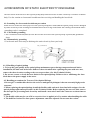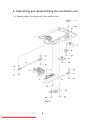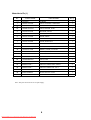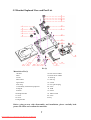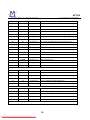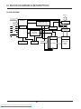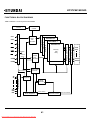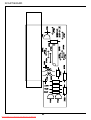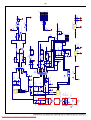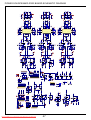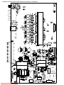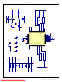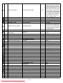
1
SERVICE MANUAL
Dk960S
TUNED
ST.
3D
MEM
AM
ALL FM
VOL1
Downloaded From TheatreSystem-Manual.com Manuals
VOL2
C ONTE NTS
1.
S AF E T Y P R IC AUT IONS
2.
P R E V E NT ION OF E LE C T R O S TATIC DIS C HAR G E (E S D)TO E LE C T R OS TATIC ALLY
1
S E NS IT IV E (E S )DE V IC E S
1
3.
C ONT R OL B UT T ON LOC AT IONS AND E XP LANAT IONS
2
4.
P R E V E R TION OF S TATIC E LE C T R IC IT Y DIS C HAR G E
4
5.
AS S E MB LING AND DIS AS S E MB LING T HE ME C HANIS M UNIT
5
5.1
OP T IC AL P IC K UP UNIT E XP LOS E D V IE W AND PAR T LIS T
5
5.2
B R AC K E T E XP LOS E D V IE W AND PAR T LIS T
7
5.3
MIS C E LLANE OUS
8
6.
E LE C T R IC AL C ONF IR MAT ION
9
6.1
V IDE O OUT P UT (LUMINANC E S IG NAL) C ONF IR MAT ION
9
6.2
V IDE O OUT P UT (C HR OMINANC E S IG NAL) C ONF IR MATION
10
7.
MP E G B OAR D C HE C K WAVE F OR M
11
8.
IC B LOC K DIAG R AM & DE S C R IP T ION
12
8.1
MT 1336
12
8.2
MT 1379
20
8.3
U214 HY 29F 800
36
8.4
HY57V641620HG
39
9.
S C HE MAT IC & P C B WIR ING DIAG R AM
42
10.
S PAR E PAR T S LIS T
59
Downloaded From TheatreSystem-Manual.com Manuals
1. SAFETY PREAUTIONS
1.1 GENERAL GUIDELINES
1. When servicing, observe the original lead dress. if a short circuit is found, replace all parts which have
been overheated or damaged by the short circuit.
2. After servicing, see to it that all the protective devices such as insulation barrier, insulation papers
shields are properly installed.
3. After servicing, make the following leakage current checks to prevent the customer from being exposed
to shock hazards.
2.PREVENTION OF ELECTRO STATIC DISCHARGE(ESD)TO
ELECTROSTATICALLY SENSITIVE(ES)DEVICES
Some semiconductor(solid state)devices can be damaged easily by static electricity. Such components
commonly are called Electrostatically Sensitive(ES)Devices. Examples of typical ES devices are integrated
circuits and some field-effect transistors and semiconductor chip components. The following techniques
should be used to help reduce the incidence of component damage caused by electro static discharge(ESD).
1. Immediately before handling any semiconductor component or semiconductor-equipped assembly, drain
off any ESD on your body by touching a known earth ground. Alternatively, obtain and wear a commercially
availabel discharging ESD wrist strap, which should be removed for potential shock reasons prior to
applying power to the unit under test.
2. After removing an electrical assembly equipped with ES devices,place the assembly on a conductive
surface such as alminum foil, to prevent electrostatic charge buildup or exposure of the assembly.
3. Use only a grounded-tip soldering iron to solder or unsolder ES devices.
4. Use only an anti-static solder removal device. Some solder removal devices not classified as anti-static
(ESD protected)can generate electrical charge sufficient to damage ES devices.
5. Do not use freon-propelled chemicals. These can generate electrical charges sufficient to damage ES
devices.
6. Do not remove a replacement ES device from its protective package until immediately before you are
ready to install it. (Most replacement ES devices are packaged with leads electrically shorted together by
conductive foam, alminum foil or comparable conductive material).
7. Immediately before removing the protective material from the leads of a replacement ES device, touch
the protective material to the chassis or circuit assembly into which the device will be installed.
Caution
Be sure no power is applied to the chassis or circuit, and observe all other safety precautions.
8. Minimize bodily motions when handling unpackaged replacement ES devices. (Otherwise harmless motion
such as the brushing together of your clothes fabric or the lifting of your foot from a carpeted floor can
generate static electricity(ESD).
notice (1885x323x2 tiff)
1
Downloaded From TheatreSystem-Manual.com Manuals
3.Control Button Locations and Explanations
Front Panel Illustration
3
2
4
TUNED
5
ST.
3D
MEM
AM
ALL FM
VOL1
6
7
8
9 10 11
12
13
14
VOL2
15
POWER switch
6
PLAY button
11
DVD MODE: NEXT button
TUNER MODE: TUNING button
2
Disc tray
7
STOP button
12
MIC 1 jack
3
OPEN/CLOSE button
8
FUNCTION button
13
MIC 2 jack
4
VFD display window
9
DVD MODE: PAUSE button
TUNER MODE: BAND button
14
MIC VOLUME 1 knob
5
VOLUME knob
DVD MODE PREV button
TUNER MODE TUNING button
15
MIC VOLUME 2 knob
10
2
Downloaded From TheatreSystem-Manual.com Manuals
Control Button Locations and Explanations (Continued)
STANDBY button
Remote Control Illustration
Enter or exit the standby mode.
2
AUDIO button
Change the audio language.
3
EJECT
STANDBY
39
AUDIO
SUBTITLE ANGLE FUNCTION
2
38
3
37
1
4
3
2
4
5
6
7
8
9
0
+10
GOTO
PANEL
P/N
ZOOM
OSD
5
Open/close the virtual keyboard function.
6
36
34
33
7
8
10
PLAY
PAUSE
SLOW
REPEAT
MIC
15
16
17
18
VOCAL
A-B
INFO
SLEEP
PRESET
MUTE
SAVE
TUNING
SPEAKERS
13
Slow playback.
MIC button
30
15
REPEAT button
29
16
28
17
27
26
25
Q-PLAY
Repeat playback.
TREBLE
SLEEP button
Sleep timer.
VOCAL Button
Select the Karaoke sing-along mode
18
SAVE/LOGO button
Stations saving button, up to 20 FM/AM stations can
be saved respectively/Set the played image as the
power-on logo
19
BASS
SLOW button
14
MAN/AUTO
BAND
PAUSE button
Karaoke operation menu.
LOGO
19
20
PLAY button
Normal playback.
STOP
MAIN
VOL
13
14
SELECT button
SETUP button
Pause playback.
32
RETURN
31
11
12
DIRECTION ARROWS
Function setup.
11
SELECT
SETUP
TITLE button
UP/DOWN/LEFT/RIGHT DIRECTION ARROW.
9
12
9
10
P/N button
DVD titles.
MENU
8
NUMBERED buttons
PANEL button
Switch the TV system between PAL, NTSC and AUTO.
35
TITLE
Change subtitle languages/Switch JPEG display modes.
4
7
5
6
SUBTITLE button
VOL
TUNING +/- buttons
Tuning up/down stations.
PS/IS
24
21
23
22
20
FWD/REW button
Fast forward/backward playback.
MAN/AUTO buttou/Q-PLAY button
Manual/automatic tuning switch/Skip the advertisement/
warning and play the DVD directly.
21
BAND button/IS/PS button
FM/AM switch/Switch Video output to the interlacing
mode./Switch video to the progressive Y Pb Pr
mode.
22
BASS +/- button
Increase/decrease bass.
23
32
Increase/decrease treble.
RETURN button
24
Back to the previous menu.
33
25
26
PREVIOUS/NEXT button
OSD button
Select previous/next chapter or track when playing.
27
GOTO button
28
27
FUNCTION button
Downloaded From TheatreSystem-Manual.com Manuals
INFO button
Switch new user interface.
A-B button
Repeat the selected section A-B.
EJECT button
Open/Close the disc tray.
29
27
30
DISC/RADIO/AUX IN switch.
39
MAIN VOL button
Increase/decrease the master volume.
ANGLE button
Camera angles switch, MP3/JPEG playback modes switch.
38
MUTE button
Turn off/on audio outputs
Play from the desired point.
37
PRESET +/- button
Select the preset channels.
Display the disc information.
36
SPEAKERS button
Select power amplifier's channel volume.
ZOOM button
Zoom in/out the playing frame.
35
VOL +/- button
Increase/decrease power amplifier's channel volume.
MENU button
Display the disc menu, PBC ON/OFF button.
34
TREBLE +/- button
31
3
STOP button
Stop playback.
4.PREVENTION OF STATIC ELECTRICITY DISCHARGE
The laser diode in the traverse unit (optical pickup)may brake down due to static electricity of clothes or human
body. Use due caution to electrostatic breakdown when servicing and handling the laser diode.
4.1.Grounding for electrostatic breakdown prevention
Some devices such as the DVD player use the optical pickup(laser diode)and the optical pickup will be damaged
by static electricity in the working environment.Proceed servicing works under the working environment where
grounding works is completed.
4.1.1. Worktable grounding
1. Put a conductive material(sheet)or iron sheet on the area where the optical pickup is placed,and ground the
sheet.
4.1.2.Human body grounding
1 Use the anti-static wrist strap to discharge the static electricity from your body.
safety_3 (1577x409x2 tiff)
4.1.3.Handling of optical pickup
1. To keep the good quality of the optical pickup maintenance parts during transportation and before
installation, the both ends of the laser diode are short-circuited.After replacing the parts with new ones,
remove the short circuit according to the correct procedure. (See this Technical Guide).
2. Do not use a tester to check the laser diode for the optical pickup .Failure to do so willdamage the laser
diode due to the power supply in the tester.
4.2. Handling precautions for Traverse Unit (Optical Pickup)
1. Do not give a considerable shock to the traverse unit(optical pickup)as it has an extremely high-precise
structure.
2. When replacing the optical pickup, install the flexible cable and cut is short land with a nipper. See the
optical pickup replacement procedure in this Technical Guide. Before replacing the traverse unit, remove
the short pin for preventingstatic electricity and install a new unit.Connect the connector as short times as
possible.
3. The flexible cable may be cut off if an excessive force is applied to it.Use caution when handling the cable.
4. The half-fixed resistor for laser power adjustment cannot be adjusted. Do not turn the resistor.
4
Downloaded From TheatreSystem-Manual.com Manuals
5. Assembling and disassembling the mechanism unit
5.1 Optical pickup Unit Explosed View and Part List
Pic (1)
5
Downloaded From TheatreSystem-Manual.com Manuals
Materials to Pic (1)
No.
PARTS CODE
PARTS NAME
Q ty
14692200
SF-HD60
1
1
1EA0311A06300
ASSY, CHASSIS, COMPLETE
1
2
1EA0M10A15500
ASSY, MOTOR, SLED
1
Or
1EA0M10A15501
ASSY, MOTOR, SLED
1
3
1EA2451A24700
HOLDER, SHAFT
3
4
1EA2511A29100
GEAR, RACK
1
5
1EA2511A29200
GEAR, DRIVE
1
6
1EA2511A29300
GEAR, MIDDLE, A
1
7
1EA2511A29400
GEAR, MIDDLE, B
1
8
1EA2744A03000
SHAFT, SLIDE
1
9
1EA2744A03100
SHAFT, SLIDE, SUB
1
10
1EA2812A15300
SPRING, COMP, TYOUSEI
3
11
1EA2812A15400
SPRING, COMP, RACK
1
21
1EA0B10B20100
ASSY, PWB
1
Or
1EA0B10B20200
ASSY, PWB
1
31
SEXEA25700---
SPECIAL SCREW BIN+-M2X11
3
32
SEXEA25900---
SPECIAL SCREW M1.7X2.2
2
33
SFBPN204R0SE-
SCR S-TPG PAN 2X4
2
34
SFSFN266R0SE-
SCR S-TPG FLT 2.6X6
1
35
SWXEA15400---
SPECIAL WASHER 1.8X4 X0.25
2
Note : This parts list is not for service parts supply.
6
Downloaded From TheatreSystem-Manual.com Manuals
5.2 Bracket Explosed View and Part List
Pic (2)
Materials to Pic(2)
1.bracket
2.belt
3.screw
4.belt wheel
5.gearwheel
6.iron chip
7. Immobility mechanism equipment
8. Magnet
9. Platen
10. Bridge bracket
11. screw
12. screw
13. Big bracket
14. front silicon rubber
15. Back silicon rubber
16. Pick-up
17. Pick-up
18. switch
19. Five-pin flat plug
20. screw
21. PCB
22. motor
23. Motor wheel
24. screw
25.tray
Before going process with disassembly and installation, please carefully both
peruse the chart and confirm the materials.
7
Downloaded From TheatreSystem-Manual.com Manuals
5.3 MISCELLANEOUS
5.3.1 Protection of the LD(Laser diode)
Short the parts of LD circuit pattern by soldering.
5.3.2 Cautions on assembly and adjustment
Make sure that the workbenches,jigs,tips,tips of soldering irons and measuring instruments are
grounded,and that personnel wear wrist straps for ground.
Open the LD short lands quickly with a soldering iron after a circuit is connected.
Keep the power source of the pick-up protected from internal and external sources of electrical
noise.
Refrain from operation and storage in atmospheres containing corrosive gases (such as H2S,SO2,
NO2 and Cl2)or toxic gases or in locations containing substances(especially from the organic silicon,cyan,
formalin and phenol groups)which emit toxic gases.It is particularly important to ensure that none of the
above substances are present inside the unit.Otherwise,the motor may no longer run.
8
Downloaded From TheatreSystem-Manual.com Manuals
6.Electrical Confirmation
6.1. Video Output (Luminance Signal) Confirmation
DO this confirmation after replacing a P.C.B.
Measurement point
Mode
Disc
Video output terminal
Color bar 75%
PLAY(Title 46):DVDT-S15
PLAY(Title 12):DVDT-S01
DVDT-S15
or
DVDT-S01
Measuring equipment,tools
Confirmation value
200mV/dir,10 sec/dir
1000mVp-p±30mV
Purpose:To maintain video signal output compatibility.
1.Connect the oscilloscope to the video output terminal and terminate at 75 ohms.
2.Confirm that luminance signal(Y+S)level is 1000mVp-p±30mV
9
Downloaded From TheatreSystem-Manual.com Manuals
6.2 Video Output(Chrominance Signal) Confirmation
Do the confirmation after replacing P.C.B.
Measurement point
Mode
Disc
Video output terminal
Color bar 75%
PLAY(Title 46):DVDT-S15
PLAY(Title 12):DVDT-S01
DVDT-S15
or
DVDT-S01
Measuring equipment,tools
Screwdriver,Oscilloscope
200mV/dir,10 sec/dir
Confirmation value
621mVp-p±30mV
Purpose:To maintain video signal output compatibility.
1.Connect the oscilloscope to the video output terminal and terminate at 75 ohme.
2.Confirm that the chrominance signal(C)level is 621 mVp-p±30mV
10
Downloaded From TheatreSystem-Manual.com Manuals
7.MPEG BOARD CHECK WAVEFORM
7.1 27MHz WAVEFORM
DIAGRAM
7.2 IC5L0380R PIN.2 WAVEFORM DIAGRAM
11
Downloaded From TheatreSystem-Manual.com Manuals
MT1336
PRELIMINARY, SUBJ ECT TO CHANGE WITHOUT NOTICE
MTK CONFIDENTIAL, NO DISCLOSURE
8. IC BLOCK DIAGRAM & DESCRIPTION
8.1 MT1336
GENERAL DESCRIPTION
M T 1 3 3 6 i s a h i g h p e r f o r m a n c e C M O S a n a l o g f r o n t -e n d I C f o r b o t h C D _ R O M d r i v e r u p t o 4 8 X S a n d
D V D - R O M d r i v e r u p t o 1 6 X S . I t a l s o s u p p o r t s D V D- R A M r e a d u p t o 4 X S V e r s i o n 2 . I t c o n t a i n s s e r v o a m p li f i e r s
t o g e n e r a t e f o c u s i n g e r r o r , 3-b e a m t r a c k i n g e r r o r , 1 b e a m r a d i a l p u s h -p u l l s i g n a l , R F l e v e l a n d S B A D f o r s e r v o
f u n c t i o n s . I t a l s o i n c l u d e s D P D t r a c k i n g e r r o r s i g n a l f o r D V D _ R O M a p p l i c a t i o n . F o r D V D- R A M d i s k s , t h e r e a r e
a l s o D i f f e r e n t i a l P u s h -P u l l ( D P P ) m e t h o d f o r g e n e r a t i n g t r a c k i n g s i g n a l a n d D i f f e r e n t i a l A s t i g m a t i c D e t e c t i o n
(DAD) for processing focusing signal. Programmable equalizer and AGC circuits are also incorporated in this
chip to optimize read channel performance. In addition, this chip has dual automatic laser power control circuits
f o r D V D- R O M ( D V D-R A M )
and
C D -R O M s e p e r a t e l y a n d r e f e r e n c e v o l t a g e g e n e r a t o r s t o r e d u c e e x t e r n a l
c o m p o n e n t s . P r o g r a m m a b l e f u n c t i o n s a r e i m p l e m e n t e d b y t h e a c c e s s o f i n t e r n a l r e g i s t e r t h r o u g h b i -d i r e c t i o n a l
serial port to configure modes selection.
FEATURES
n
RF equalizer with programmable
fc
from 3MHz to 70 MHz and programmable boost from 3dB to
13dB.
n
M T 1 3 3 6 s u p p o r t s a t l e a s t e i g h t d i f f e r e n t k i n d s o f p i c k-u p h e a d s w i t h v e r s a t i l e i n p u t c o n f i g u r a t i o n f o r
both RF input stages and servo signal blocks.
n
Versatile on -line AGC.
n
3 beams tracking error signal generator for CD_ROM application.
n
One beam differential phase tracking error (DPD) generator for DVD_ROM application.
n
Differential push pull tracki ng error (DPP) generator for DVD_RAM application.
n
Focusing error signal generator for CD-ROM, DVD-ROM and DVD-RAM (DAD method).
n
RF level signal generator.
n
Sub-beam added signal for 3 beams CD_ROM.
n
One beam push -pull signal generator for central servo application.
n
High speed RF envelop detection circuit with bandwidth up to 400KHz for CD-ROM.
n
Defect and Blank detection circuits.
n
Dual automatic laser power control circuits with programmable level of LD monitor voltage.
n
Vref=1.4V voltage and V2ref=2.8V voltage generators.
n
V20=2.0V voltage for pick -up head reference.
n
Bi-directional serial port to access internal registers.
12
Downloaded From TheatreSystem-Manual.com Manuals
MT1336
PRELIMINARY, SUBJ ECT TO CHANGE WITHOUT NOTICE
MTK CONFIDENTIAL, NO DISCLOSURE
OSP
DVDA
OSN
CDA
DVDB
RFOP
ATTENUATOR
INPUT MUX
VGA
EQ
RFON
CDB
DVDC
LRFRP
CDC
DEFECT
DVDD
HRFRP
CDD
DVDRFIN
CRTP
ENVELOP
CRTPLP
DETECTOR
DVDRFIP
AGC
MA
CSO
MB
MC
LVL
MD
DPD
SA
TEO
SB
FEO
SC
REFCOS
SD
SBAD
PCS
HALLCOS
COSPHI
DPFN
REFSIN
DPFO
HALLSIN
IR
SINPHI
DPDMUTE
TE
DVD
MDI2
APC
TPI
TNI
LDO2
CDFOP
RF
CDFON
LEVEL
RFGC
RFGCU
MDI1
CD
FE
RFGCI
APC
AGC1
LDO1
AGC2
CENTRAL
AGC3
SERVO
RFSUBO
WOBSO
UDGATE
IDGATE
WOBBLE
VFO13
DET
SDATA
SERIAL
V20
REF and 2VREF
V2REFO
PORT
Voltage Generator
VREFO
MT1336 FUNCTION BLOCKS DIAGRAM
13
Downloaded From TheatreSystem-Manual.com Manuals
SLCK
SDEN
MT1336
CDFOP
SD
SC
AVDD
IR
AGND
SB
SA
MD
MC
TNI
TPI
SVDD
CDFON
WAGND
SGND
WAVDD
AGC1
MDI2
AGC3
AGC2
LDO2
LDO1
MDI1
MTK CONFIDENTIAL, NO DISCLOSURE
128
127
126
125
124
123
122
121
120
119
118
117
116
115
114
113
112
111
110
109
108
107
106
105
104
103
WGND
RFSUBO
PRELIMINARY, SUBJ ECT TO CHANGE WITHOUT NOTICE
MT1336
DVD-ROM
With
DVD_RAM
Read
GND
UDGATE
HDGATE
IO0
IO1
IO2
IO3
IO4
IO5
IO6
IO7
IO8
IO9
IOA
IOB
VDDS
XCK16M
SCLK
AVDDT
V2REFO
VREFO
V20
FEO
LVL
CSO
TEO
VDDP
DEFECT
LRFRP
HRFRP
CRTP
CRTPLP
TRLPA
TRLP
HTRC
GNDP
DPFN
DPFO
AGNDX
AGNDX
AGNDX
VDD
VFO13
12
13
14
15
16
17
18
19
20
21
22
23
24
25
26
27
28
29
30
31
32
33
34
35
36
37
38
MT1336 PIN ASSIGNMENT
14
Downloaded From TheatreSystem-Manual.com Manuals
AGNDP
AGNDX
AVDDP
AGNDT
TM4
DPDMUTE
TM1
TM2
TM3
GNDS
SDEN
SDATA
RST
RFOP
RFON
AGNDO
1
2
3
4
5
6
7
8
9
10
11
39
40
41
42
43
44
45
46
47
48
49
50
51
52
53
54
55
56
57
58
59
60
61
62
63
64
WOBSO
WVDD
AGNDX
AGNDX
AVDDO
102
101
100
99
98
97
96
95
94
93
92
91
90
89
88
87
86
85
84
83
82
81
80
79
78
77
76
75
74
73
72
71
70
69
68
67
66
65
MB
MA
DVDA
DVDB
DVDC
DVDD
DVDRFIP
DVDRFIN
CDA
CDB
CDC
CDD
OSN
OSP
RFGC
RFGCU
RFGCI
CEQP
CEQN
AGNDX
AGNDX
MON
MOP
SW1
SW2
SWO
SINPHI
REFSIN
HALLSIN
AGNDM
REFCOS
HALLCOS
COSPHI
AVDDM
AGNDX
AVDDF
VCON
AGNDF
MT1336
PRELIMINARY, SUBJ ECT TO CHANGE WITHOUT NOTICE
MTK CONFIDENTIAL, NO DISCLOSURE
MT1336 PIN DESCRIPTIONS
Pin Numbers
Symbol
Type
Description
DEFECT
Digital Output
56
SCLK
Digital Input
RF serial clock input
58
SDEN
Digital Input
RF serial data enable
59
SDATA
Digital IO
60
RST
Digital input
Reset (active high)
55
XCK16M
Digital Input
16.9MHz for verification
LQFP128
RF Flag Interface
23
Flag of bad data output status
RF SIO interface
RF serial data IO
RF SERVO interface
40
UDGATE
Digital Input
Con trol signal for DVD-RAM
41
IDGATE
Digital Input
Control signal for DVD -RAM
38
VFO13
Digital Input
DVD -RAM Header signal
RF
100
DVDA
Analog input
AC coupled DVD RF signal input A
99
DVDB
Analog Input
AC coupled DVD RF signal input
98
DVDC
Analog Input
AC coupled DVD RF signal input C
97
DVDD
Analog Input
AC coupled DVD RF signal input D
95
DVDRFIN
Analog Input
AC coupled DVD RF signal input RFIN
96
DVDRFIP
Analog Input
AC coupled DVD RF signal input RFIP
94
CDA
Analog Input
AC coupled CD RF signal input A
93
CDB
Analog Input
AC coupled CD RF signal input B
92
CDC
Analog Input
AC coupled CD RF signal input C
91
CDD
Analog Input
AC coupled CD RF signal input D
90
OSN
Analog
RF Offset cancellation capacitor connecting
89
OSP
Analog
RF Offset cancellation capacitor connecting
85
CEQP
Analog
RF Offset cancellation capacitor connecting
84
CEQN
Analog
RF Offset cancellation capacitor connecting
88
RFGC
Analog
RF AGC loop capacitor connecting for DVD -ROM
15
Downloaded From TheatreSystem-Manual.com Manuals
B
MT1336
PRELIMINARY, SUBJ ECT TO CHANGE WITHOUT NOTICE
MTK CONFIDENTIAL, NO DISCLOSURE
87
RFGCU
Analog
RF AGC loop capacitor connecting for DVD -RAM
86
RFGCI
Analog
RF AGC loop capacitor connecting for DVD -RAM
101
MA
Analog Input
DC coupled DVD-RAM main-beam RF signal input A
102
MB
Analog Input
DC coupled DVD-RAM main-beam RF signal input B
103
MC
Analog Input
DC coupled DVD-RAM main-beam RF signal input C
104
MD
Analog Input
DC coupled DVD-RAM main-beam RF signal input D
105
SA
Analog Input
DC coupled DVD-RAM sub-beam RF signal input A
106
SB
Analog Input
DC coupled DVD-RAM sub-beam RF signal input B
110
SC
Analog Input
DC coupled DVD-RAM sub-beam RF signal input C
111
SD
Analog Input
DC coupled DVD-RAM sub-beam RF signal input D
108
IR
Analog
External current bias resistor (R=20K)
119
AGC1
Analog
Wobble AGC loop1 capacitor
121
AGC2
Analog
Wobble AGC loop2 capacitor
122
AGC3
Analog
Wobble AGC loop3 capacitor
127
RFSUBO
Analog output
Header push-pull RF output signal
1
WOBSO
Digital output
Wobble signal output
6
RFOP
Analog output
RF positive output
7
RFON
Analog output
RF negative output
32
DPFN
Analog
DPD amplifier negative input
33
DPFO
Analog
DPD amplifier output
61
DPDMUTE
Digital input
DPD mute control input
116
TNI
Analog Input
3 beam satellite PD signal negative input
115
TPI
Analog Input
3 beam satellite PD signal positive input
21
TEO
Analog Output
TRACKING ERROR
FOCUSING ERROR & RF LEVEL
Tracking error output
& CENTRAL SERVO SIGNAL
112
CDFOP
Analog Input
CD focusing error positive input
113
CDFON
Analog Input
CD focusing error negative input
18
FEO
Analog Output
Focusing error output
19
LVL
Analog Output
RF level output
20
CSO
Analog output
Central servo signal output
ALPC
16
Downloaded From TheatreSystem-Manual.com Manuals
MT1336
PRELIMINARY, SUBJ ECT TO CHANGE WITHOUT NOTICE
MTK CONFIDENTIAL, NO DISCLOSURE
124
MDI1
Analog Input
125
LDO1
Analog Ou tput
123
MDI2
Analog Input
126
LDO2
Analog Output
26
CRTP
Analog
RF top envelop filter capacitor connecting
27
CRTPLP
Analog
Defect level filter capacitor connecting
25
HRFRP
Analog output
High frequency RF ripple output or Blank detector’s output
24
LRFRP
Analog output
Low frequency RF ripple output
67, 69
AVDD
Power
65, 73
AGND
GND
64
AVDD
Power
DPD Power
62
AGND
GND
DPD GND
109
AVDD
Power
107
AGND
GND
RF path GND
114
SVDD
Power
Servo Power
117
SGND
GND
2,120
WAVDD
Power
128,118
WAGND
GND
5
AVDDO
Power
Power for RF output
8
AGNDO
GND
GND for RF output
14
AVDDT
Power
12
AGNDT
GND
GND for Trimming PAD
22
VDDP
Power
Peak Detection Power
31
GNDP
GND
Peak Detection GND
37,54
VDD
Power
Serial I/O Power
39,57
GND
GND
Serial I/O GND
Laser power monitor input
Laser driver output
Laser power monitor input
Laser driver output
RF RIPPLE
POWER
Master PLL Filter power
GND for Master PLL Filter
RF path Power
Servo GND
Wobble Power
Wobble GND
Power for Trimming PAD
REFERENCE VOLTAGE
16
VREFO
Analog output
Reference voltage 1.4V
15
V2REFO
Analog output
Reference voltage 2.8V
17
V20
Analog Output
Reference voltage 2.0V
17
Downloaded From TheatreSystem-Manual.com Manuals
MT1336
PRELIMINARY, SUBJ ECT TO CHANGE WITHOUT NOTICE
MTK CONFIDENTIAL, NO DISCLOSURE
ALPC TRIMMING
9
TM1
Analog input
Trimming pin for ALPC1
10
TM2
Analog input
Trimming pin for ALPC1
11
TM3
Analog input
Trimming pin for ALPC2
13
TM4
Analog input
Trimming pin for ALPC2
HIGH SPEED TRACK COUNTING
29
TRLP
Analog
Low-pass filter capacitor connecting
28
TRLPA
Analog
Low-pass filter capacitor connecting
30
HTRC
Digital output
High speed track counting digital output
74
HALLSIN
Analog input
Negative input of amplifier for hall sensor signal
75
REFSIN
Analog input
Positive input of amplifier for hall sensor signal
76
SINPHI
Analog output
Amplifier output for hall sensor signal
71
HALLCOS
Analog input
Negative input of amplifier for hall sensor signal
72
REFCOS
Analog input
Positive input of amplifier for hall sensor signal
70
COSPHI
Analog output
Amplifier output for hall sensor signal
PCS
FOR MONITOR ONLY
81
MON
Analog output
80
MOP
Analog output
66
VCON
Analog output
77
SWO
Analog output
Output from mux of SW1 & SW2
78
SW2
Analog input
External input for servo input select
79
SW1
Analog input
External input for servo input select
FOR SERIAL I/O
42
IO0
43
IO1
44
IO2
45
IO3
46
IO4
47
IO5
18
Downloaded From TheatreSystem-Manual.com Manuals
MT1336
PRELIMINARY, SUBJ ECT TO CHANGE WITHOUT NOTICE
48
IO6
49
IO7
50
IO8
51
IO9
52
IOA
53
IOB
MTK CONFIDENTIAL, NO DISCLOSURE
19
Downloaded From TheatreSystem-Manual.com Manuals
MT1379
Progressive Scan DVD Player Combo Chip
Specificationsaresubjecttochangewithoutnotice
8.2 MT1379
n Super Integration DVD player single chip
§
Servo controller and data channel processing
§
MPEG-1/MPEG-2/JPEG video decoding
Dolby AC-3/DTS/DVD -Audio audio decoding
§
§
§
§
§
§
Built-in TV encoder
Built-in progressive video output
§
Video input port and audio/SPDIF input port
§
§
§
§
§
§
Built-in DSP for digital servo control
§
Built-in 8032 micro controller
§
Built-in internal 373 and 8-bit programmable
lower address port
§
1024-bytes on-chip RAM
Up to 2M bytes FLASH-programming interface
Supports 5/3.3-Volt. FLASH interface
§
§
§
§
Built-in a frequency programmable clock to µP
and RSPC Decoder to optimize the performance
over power
§
§
§
Provides interface with analog front-end
processor
Analog data slicer for small jitter capability
§
§
Built-in high performance data PLL for chann el
data demodulation
§
EFM/EFM+ data demodulation
Enhanced channel data frame sync protection &
DVD-ROM sector sync protection
§
§
§
n Servo Control and Spindle Motor Control
§
§
Programmable frequency error gain and phase
error gain of spindle PLL to control spindle motor
on CLV and CAV mode
Provide a varipitch speed control for CLV and CAV
mode
Built-in ADCs and DACs for digital servo control
§
Provide 2 general PWM
§
20
Downloaded From TheatreSystem-Manual.com Manuals
Supports power-down mode
Supports additional serial port
n DVD-ROM/CD-ROM Decoding Logic
DVD-ROM up to 8XS
CD-ROM up to 24XS
n Channel Data Processor
§
§
§
n Speed Performance on Servo and Decoding
§
Tray control can be PWM output or digital output
n Host Micro controller
Unified track buffer and A/V decoding buffer
Video processing for scaling and video quality
enhancement
OSD & Sub-picture decoding
Built-in clock generator
§
§
Supports CD-ROM Mode 1, CD-ROM XA Mode 2
Form 1, CD-ROM XA Mode 2 Form 2, and CD-DA
formats
High-speed ECC logic capable of correcting one
error per each P-codeword or Q-codeword
Automatic sector Mode and Form detection
Automatic sector Header verification
8-bit counter for decode completion check
Programmable descrambling and error
correction schemes
Automatically repeated error corrections
8-bit C2 Pointer counter
Decoder Error Notification Interrupt that signals
various decoder errors
Provide error correction acceleration
n Buffer Memory Controller
§
Supports 16Mb/32Mb/64Mb/128Mb SDRAM
§
§
Supports 16-bit/32-bit SDRAM data bus interface
Build in a DRAM interface programmable clock to
optimize the DRAM performance
Provide the self-refresh mode SDRAM
§
Programmable DRAM access cycle and refresh
§
MT1379
PRELIMINARY, SUBJECT TO CHANGE WITHOUT NOTICE
§
MTK CONFIDENTIAL, NO DISCLOSURE
§
cycle timings
Block-based sector addressing
§
§
Programmable buffering counter for buffer status
tracking
§
Maximum DRAM speed is 133MHz
Support 5/3.3-Volt. DRAM Interface
§
§
§
n Video Decode
§
§
Decodes MPEG1 video and MPEG2 main level,
main profile video (720/480 and 720x576)
Maximum input bit-rate of 15Mbits/sec
§
Smooth digest view function with I, P and B
picture decoding
§
Baseline, extended-sequential and progressive
JPEG image decoding
§
RLE and non-RLE BMP image decoding
Support CD-G titles
§
§
§
§
§
§
§
§
§
§
HDCD certified
§
Six 54MHz/12bit DA converters
Support NTSC, PAL-BDGHI, PAL-N, PAL-M
interlace TV format and 480p, 576p progressive
TV format
Automatically turn off unconnected channel(s).
Support PC monitor (VGA)
§
Support Macrovision 7.1
§
256/16 color RLC format OSD
Automatic scrolling of OSD image
§
Provides 4 -color/32x32-pixel hardware cursor
Fade-in, Fade out, and Wipe functions as
specified in the DVD-Audio Specification and
other slide show transition effects
Progressive scan output
n Progressive Output
§
Automatic detect film or video source
§
3:2 pull down source detection
Advanced Motion adaptive de-interlace
Minimum external memory requirement
§
Decoder format supports:
- Dolby Digital (AC -3) decoding
§
n Audio/Video Output
§
- MPEG-1 layer 1/layer 2 audio decoding
- MPEG-2 layer1/layer2 2 -channel audio decoding
- Dolby Pro Logic decoding
- High Definition Compatible Digital (HDCD)
decoding
§
§
Line-in/SPDIF-in for versatile audio processing
CCIR601/656 video input port
Support picture-in-picture for video decoding and
input source
n Outline
Up to 6 channel linear PCM output for DVD Audio
/ DVD Video
21
Downloaded From TheatreSystem-Manual.com Manuals
§
§
- DTS decoding
- MLP decoding for DVD -Audio
§
Karaoke functions
- Microphone echo with adjustable echo level,
echo -depth and delay length
- Microphone tone control with three custom
second-order IIR filter
- Vocal mute/vocal assistant
- Key shift up to +/- 8 keys controlled by 1/2 key
n TV Encoder
Arbitrary ratio vertical/horizontal scaling of video,
from 0.25X to 256X
65535/256/16/4/2-color bitmap format OSD,
n Audio Processing
§
- PCM / bit stream / mute mode
- Custom IEC latency up to 2 frames
Pink noise and white noise generator
Channel equalizer
3D surround processing include virtual surround
and speaker separation
Power-down control
§
n Video/OSD/SPU/HLI Processor
Downmix function
Support IEC 60958/61937 output
§
§
216-pin LQFP package
3.3/2.5-Volt. Dual operating voltages
MT1379
PRELIMINARY, SUBJECT TO CHANGE WITHOUT NOTICE
MTK CONFIDENTIAL, NO DISCLOSURE
P IN D EFINITIONS
Pin Number
Symbol
Type
1
IREF
Analog Input
2
3
4
5
6
7
8
9
10
11
12
13
14
PLLVSS
LPIOP
LPION
LPFON
LPFIP
LPFIN
LPFOP
JITFO
JITFN
PLLVDD3
FOO
TRO
TROPENPWM
Ground
Analog Output
Analog Output
Analog output
Analog Input
Analog Input
Analog Output
Analog Output
Analog Input
Power
Analog Output
Analog Output
Analog Output
15
16
17
18
19
20
21
22
PWMOUT1
PWMOUT2
DVDD2
DMO
FMO
DVSS
FG
HIGHA0
23
HIGHA1
24
HIGHA2
25
HIGHA3
26
HIGHA4
27
HIGHA5
28
DVSS
Analog Output
Analog Output
Power
Analog Output
Analog Output
Ground
Input
Inout
2~16MA, SR
PU
Inout
2~16MA, SR
PU
Inout
2~16MA, SR
PU
Inout
2~16MA, SR
PU
Inout
2~16MA, SR
PU
Inout
2~16MA, SR
PU
Grou nd
Description
Current reference input. It generates reference current for data
PLL.
Connect an ext ernal 100K resistor to this pin and PLLVSS.
Ground pin for data PLL and related analog circuitry
Positive output of the low pass filter
Negative output of the low pass filter
Negative output of loop filter amplifier
Positive input of loop filter amplifier
Negative input of loop filter amplifier
Positive output of loop filter amplifier
RF jitter meter output
Negative input of the operation amplifier for RF jigger meter
3.3V power pin for data PLL and related analog circuitry
Focus servo output. PDM output of focus servo compensator
Tracking servo output. PDM output of tracking servo compensator
Tray open output, controlled by microcontroller.
This is PWM output for TRWMEN27hRW2=1 or is digital output for
TRWMEN27hRW2=0
The 1st general PWM output
The 2nd general PWM output
2.5V power pin for internal fully digital circuitry
Disk motor control output. PWM output
Feed motor control. PWM output
Ground pin for internal fully digital circuitry
Motor Hall sensor input
Microcontroller address 8
Microcontroller address 9
Microcontroller address 10
Microcontroller address 11
Microcontroller address 12
Microcontroller address 13
Ground pin for internal digital circuitry
22
Downloaded From TheatreSystem-Manual.com Manuals
MT1379
PRELIMINARY, SUBJECT TO CHANGE WITHOUT NOTICE
MTK CONFIDENTIAL, NO DISCLOSURE
Pin Number
Symbol
Type
29
HIGHA6
30
HIGHA7
31
AD7
32
AD6
33
AD5
34
AD4
35
36
DVDD3
AD3
37
AD2
38
AD1
39
AD0
40
IOA0
41
IOA1
42
43
DVDD2
IOA2
44
IOA3
45
IOA4
46
IOA5
47
IOA6
Inout
2~16MA, SR
PU
Inout
2~16MA, SR
PU
Inout
2~16MA, SR
Inout
2~16MA, SR
Inout
2~16MA, SR
Inout
2~16MA, SR
Power
Inout
2~16MA, SR
Inout
2~16MA, SR
Inout
2~16MA, SR
Inout
2~16MA, SR
Inout
2~16MA, SR
PU
Inout
2~16MA, SR
PU
Power
Inout
2~16MA, SR
PU
Inout
2~16MA, SR
PU
Inout
2~16MA, SR
PU
Inout
2~16MA, SR
PU
Inout
2~16MA, SR
PU
Description
Microcontroller address 14
Microcontroller address 15
Microcontroller address/data 7
Microcontroller address/data 6
Microcontroller address/data 5
Microcontroller address/data 4
3.3V power pin for internal digital circuitry
Microcontroller address/data 3
Microcontroller address/data 2
Microcontroller address/data 1
Microcontroller address/data 0
Microcontroller address 0 / IO
Microcontroller address 1 / IO
2.5V power pin for internal digital circuitry
Microcontroller address 2 / IO
Microcontroller address 3 / IO
Microcontroller address 4 / IO
Microcontroller address 5 / IO
Microcontroller address 6 / IO
23
Downloaded From TheatreSystem-Manual.com Manuals
MT1379
PRELIMINARY, SUBJECT TO CHANGE WITHOUT NOTICE
MTK CONFIDENTIAL, NO DISCLOSURE
Pin Number
Symbol
Type
48
IOA7
49
A16
50
A17
51
IOA18
52
IOA19
53
IOA20
54
55
56
APLLVSS
APLLVDD3
ALE
57
IOOE#
58
IOWR#
59
IOCS#
60
61
DVSS
UP1_2
62
UP1_3
63
UP1_4
64
UP1_5
65
UP1_6
66
DVDD3
Inout
2~16MA, SR
PU
Output
2~16MA, SR
Output
2~16MA, SR
Inout
2~16MA, SR
SMT
Inout
2~16MA, SR
SMT
Inout
2~16MA, SR
SMT
Ground
Power
Inout
2~16MA, SR
PU, SMT
Inout
2~16MA, SR
SMT
Inout
2~16MA, SR
SMT
Inout
2~16MA, SR
PU, SMT
Ground
Inout
4MA, SR
PU, SMT
Inout
4MA, SR
PU, SMT
Inout
4MA, SR
PU, SMT
Inout
4MA, SR
PU, SMT
Inout
4MA, SR
PU, SMT
Power
Description
Microcontroller address 7 / IO
Flash address 16
Flash address 17
Flash address 18 / IO
Flash address 19 / IO
Flash address 20 / IO
OR Videoin Data PortB 0
Ground pin for audio clock circuitry
3.3V Power pin for audio clock circuitry
Microcontroller address latch enable
Flash output enable, active low / IO
Flash write enable, active low / IO
Flash chip select, active low / IO
Ground pin for internal digital circuitry
Microcontroller port 1 -2
Microcontroller port 1 -3
Microcontroller port 1 -4
Microcontroller port 1 -5
Microcontroller port 1 -6
3.3V power pin for internal digital circuitry
24
Downloaded From TheatreSystem-Manual.com Manuals
MT1379
PRELIMINARY, SUBJECT TO CHANGE WITHOUT NOTICE
MTK CONFIDENTIAL, NO DISCLOSURE
Pin Number
Symbol
Type
67
UP1_7
68
UP3_0
69
UP3_1
70
INT0#
71
IR
72
73
74
75
DVDD2
UP3_4
UP3_5
UWR#
76
URD#
77
78
79
80
81
82
83
84
85
86
87
DVSS
RD7
RD6
RD5
RD4
DVDD2
RD3
RD2
RD1
RD0
RWE#
88
CAS#
89
RAS#
90
RCS#
91
BA0
92
93
DVSS
RD15
Inout
4MA, SR
PU, SMT
Inout
4MA, SR
PU, SMT
Inout
4MA, SR
PU, SMT
Inout
2~16MA, SR
PU, SMT
Input
SMT
Power
Inout
Inout
Inout
2~16MA, SR
PU, SMT
Inout
2~16MA, SR
PU, SMT
Ground
Inout
Inout
Inout
Inout
Power
Inout
Inout
Inout
Inout
Output
2~16MA, SR
Output
2~16MA, SR
Output
2~16MA, SR
Output
2~16MA, SR
Output
2~16MA, SR
Ground
Inout
2~16MA, SR
PU/PD, SMT
Description
Microcontroller port 1 -7
Microcontroller port 3 -0
Microcontroller port 3 -1
Microcontroller interrupt 0, active low
IR control signal input
2.5V power pin for internal digital circuitry
Microcontroller port 3 -4
Microcontroller port 3 -5
Microcontroller write strobe, active low
Microcontroller read strobe, active low
Ground pin for internal digital circuitry
DRAM data 7
DRAM data 6
DRAM data 5
DRAM data 4
2.5V power pin for internal digital circuitry
DRAM data 3
DRAM data 2
DRAM data 1
DRAM data 0
DRAM Write enable, active low
DRAM columnaddress strobe, active low
DRAM row address strobe, active low
DRAM chip select, active low
DRAM bank address 0
Ground pin for internal digital circuitry
DRAM data 15
25
Downloaded From TheatreSystem-Manual.com Manuals
MT1379
PRELIMINARY, SUBJECT TO CHANGE WITHOUT NOTICE
MTK CONFIDENTIAL, NO DISCLOSURE
Pin Number
Symbol
Type
94
RD14
95
RD13
96
RD12
97
98
DVDD3
RD11
99
RD10
100
RD9
101
RD8
102
103
DVSS
CLK
104
CLE
105
RA11
106
RA9
107
RA8
108
109
110
DMVDD3
DMVSS
RA7
111
112
DVDD3
RA6
113
RA5
114
RA4
115
116
DVSS
DQM1
Inout
2~16MA, SR
PU/PD, SMT
Inout
2~16MA, SR
PU/PD, SMT
Inout
2~16MA, SR
PU/PD, SMT
Power
Inout
2~16MA, SR
PU/PD, SMT
Inout
2~16MA, SR
PU/PD, SMT
Inout
2~16MA, SR
PU/PD, SMT
Inout
2~16MA, SR
PU/PD, SMT
Ground
Output
2~16MA, SR
Output
2~16MA, SR
Output
2~16MA, SR
Output
2~16MA, SR
Output
2~16MA, SR
Power
Ground
Output
2~16MA, SR
Power
Output
2~16MA, SR
Output
2~16MA, SR
Output
2~16MA, SR
Ground
Output
2~16MA, SR
Description
DRAM data 14
DRAM data 13
DRAM data 12
3.3V power pin for internal digital circuitry
DRAM data 11
DRAM data 10
DRAM data 9
DRAM data 8
Ground pin for internal digital circuitry
DRAM clock
DRAM clock enable
DRAM address bit 11 or audio serial data 3 (channel 7/8)
DRAM address 9
DRAM address 8
3.3V Power pin for DRAM clock circuitry
Ground pin for DRAM clock circuitry
DRAM address 7
3.3V power pin for internal digital circuitry
DRAM address 6
DRAM address 5
DRAM address 4
Ground pin for internal digital circuitry
Mask for DRAM input/output byte 1
26
Downloaded From TheatreSystem-Manual.com Manuals
MT1379
PRELIMINARY, SUBJECT TO CHANGE WITHOUT NOTICE
MTK CONFIDENTIAL, NO DISCLOSURE
Pin Number
Symbol
Type
117
DQM0
118
BA1
119
RA10
120
121
DVDD2
RA0
122
RA1
123
RA2
124
RA3
125
126
DVSS
RD31
127
RD30
128
RD29
129
RD28
130
131
DVDD3
RD27
132
RD26
133
RD25
134
RD24
135
136
DVSS
DQM3
137
DQM2
Output
2~16MA, SR
Output
2~16MA, SR
Output
2~16MA, SR
Power
Output
2~16MA, SR
Output
2~16MA, SR
Output
2~16MA, SR
Output
2~16MA, SR
Ground
Inout
2~16MA, SR
PU/PD, SMT
Inout
2~16MA, SR
PU/PD, SMT
Inout
2~16MA, SR
PU/PD, SMT
Inout
2~16MA, SR
PU/PD, SMT
Power
Inout
2~16MA, SR
PU/PD, SMT
Inout
2~16MA, SR
PU/PD, SMT
Inout
2~16MA, SR
PU/PD, SMT
Inout
2~16MA, SR
PU/PD, SMT
Ground
Output
2~16MA, SR
Output
2~16MA, SR
Description
Mask for DRAM input/output byte 0
DRAM bank address 0
DRAM address10
2.5V power pin for internal digital circuitry
DRAM address 0
DRAM address 1
DRAM address 2
DRAM address 3
Ground pin for internal digital circuitry
DRAM data 31
DRAM data 30
DRAM data 29
DRAM data 28
3.3V power pin for internal digital circuitry
DRAM data 27
DRAM data 26
DRAM data 25
DRAM data 24
Ground pin for internal digital circuitry
Mask for DRAM input/output byte 3
Mask for DRAM input/output byte 2
27
Downloaded From TheatreSystem-Manual.com Manuals
MT1379
PRELIMINARY, SUBJECT TO CHANGE WITHOUT NOTICE
MTK CONFIDENTIAL, NO DISCLOSURE
Pin Number
Symbol
Type
138
RD23
139
RD22
140
141
DVDD2
RD21
142
RD20
143
RD19
144
RD18
145
146
DVSS
RD17
147
RD16
148
ABCK
149
ALRCK
150
151
DVDD3
ACLK
152
153
MC_DATA
SPDIF
154
ASDATA0
155
ASDATA1
156
ASDATA2
Inout
2~16MA, SR
PU/PD, SMT
Inout
2~16MA, SR
PU/PD, SMT
Power
Inout
2~16MA, SR
PU/PD, SMT
Inout
2~16MA, SR
PU/PD, SMT
Inout
2~16MA, SR
PU/PD, SMT
Inout
2~16MA, SR
PU/PD, SMT
Ground
Inout
2~16MA, SR
PU/PD, SMT
Inout
2~16MA, SR
PU/PD, SMT
Output
4MA
Inout
4MA,
PD, SMT
Power
Inout
4MA
Input
Output
2~16MA,
SR : ON/OFF
Inout
4MA
PD SMT
Inout
4MA
PD SMT
Inout
4MA
PD SMT
Description
DRAM data 23 /
Videoin Data PortA 7
DRAM data 22 /
Videoin Data PortA 6
2.5V power pin for internal digital circuitry
DRAM data 21 /
Videoin Data PortA 5
DRAM data 20 /
Videoin Data PortA 4
DRAM data 19 /
Videoin Data PortA 3
DRAM data 18 /
Videoin Data PortA 2
Ground pin for internal digital circuitry
DRAM data 17 /
Videoin Data PortA 1
DRAM data 16 /
Videoin Data PortA 0
Audio bit clock
(1) Audio left/right channel clock
(2) Trap value in power-on reset :
1 : use external 373
0: use internal 373
3.3V power pin for internal digital circuitry
Audio DAC master clock (384/256 audio sample frequency)
Microphone serial input
SPDIF output
(1)
(2)
(1)
(2)
(1)
(2)
Audio serial data 0 (left/right channel)
Trap value in power-on reset :
1 : manufactory test mode 0 : normal operation
Audio serial data 1 (surround left/surround right channel)
Trap value in power-on reset :
1 : manufactory test mode 0 : normal operation
Audio serial data 2 (center/left channel)
Trap value in power-on reset :
1 : manufactory test mode 0 : normal operation
28
Downloaded From TheatreSystem-Manual.com Manuals
MT1379
PRELIMINARY, SUBJECT TO CHANGE WITHOUT NOTICE
MTK CONFIDENTIAL, NO DISCLOSURE
Pin Number
Symbol
Type
157
ASDATA3
Inout
4MA
PD SMT
158
ASDATA4
Inout
4MA
PD SMT
159
160
161
162
DACVDDC
VREF
FS
YUV0/CIN
163
164
DACVSSC
YUV1/C
165
166
DACVDDB
YUV2/Y
Power
Analog input
Analog output
Output
4MA, SR
Ground
Output
4MA, SR
Power
Output
4MA, SR
Ground
Description
(1)
(2)
Audio serial data 3 (surround left/surround right channel)
Trap value in power-on reset :
1 : manufactory test mode 0 : normal operation
OR Videoin Data PortB 1
(1) Audio serial data 4 (center/left channel)
(2) Trap value in power-on reset :
1 : manufactory test mode 0 : normal operation
OR Videoin Data PortB 2
3.3V power pin for VIDEO DAC circuitry
Bandgap reference voltage
Full scale adjustment
Video data output bit 0 /
Compensation capacitor
Ground pin for VIDEO DAC circuitry
Video data output bit 1 /
Analog chroma output
3.3V power pin for VIDEO DAC circuitry
Video data output bit 2 /
Analog Y output
167
DACVSSB
168
YUV3/CVBS
Output
4MA, SR
Ground pin for VIDEO DAC circuitry
Video data output bit 3 /
Analog composite output
169
170
DACVDDA
YUV4/G
171
172
DACVSSA
YUV5/B
173
YUV6/R
174
ICE
3.3V power pin for VIDEO DAC circuitry
Video data output bit 4 /
Green or Y
Ground pin for VIDEO DAC circuitry
Video data output bit 5 /
Blue or CB
Video data output bit 6 /
Red or CR
Microcontroller ICE mode enable
175
BLANK#
176
VSYN
177
YUV7
178
179
DVSS
HSYN
180
SPMCLK
Power
Output
4MA, SR
Ground
Output
4MA, SR
Output
4MA, SR
Input
PD, SMT
Inout
4MA, SR
SMT
Inout
4MA, SR
SMT
Inout
4MA, SR
SMT
Ground
Inout
4MA, SR
SMT
Input
Video blank area, active low /
Videoin Field_601
Vertical sync /
Videoin Vsync_601
Video data output bit 7 /
Videoin Data PortB 3
Ground pin for internal digital circuitry
Horizontal sync /
Videoin Hsync_601
Audio DAC master clock of SPDIF input /
Videoin Data PortB 4
29
Downloaded From TheatreSystem-Manual.com Manuals
MT1379
PRELIMINARY, SUBJECT TO CHANGE WITHOUT NOTICE
MTK CONFIDENTIAL, NO DISCLOSURE
Pin Number
Symbol
Type
181
SPDATA
Input
182
183
DVDD2
SPLRCK
Power
Input
184
SPBCK
Input
185
186
187
188
DVDD3
XTALO
XTALI
PRST
189
190
191
192
193
194
195
196
197
198
199
200
201
202
203
204
205
206
207
208
209
210
211
212
213
214
215
216
DVSS
VFO13
IDGATE
DVDD3
UDGATE
WOBSI
SDATA
SDEN
SLCK
BDO
ADCVSS
ADIN
RFSUBI
TEZISLV
TEI
CSO
FEI
RFLEVEL
RFRP_DC
RFRP_AC
HRFZC
PWMVREF
PWM2VREF
ADCVDD3
RFDTSLVP
RFDTSLVN
RFIN
RFIP
Power
Output
Input
Input
PD, SMT
Ground
Output
Output
Power
Output
Input
Output
Output
Output
Input
Ground
Analog Input
Analog Input
Analog Input
Analog Input
Analog Input
Analog Input
Analog Input
A Input
Analog Input
Analog Input
A Input
A Input
Power
Analog Output
Analog Output
Analog Input
Analog Input
Description
Audio data of SPDIF input /
Videoin Data PortB 5
2.5V power pin for internal digital circuitry
Audio left/right channel clock of SPDIF input /
Videoin Data PortB 6
Audio bit clock of SPDIF input /
Videoin Data PortB 7
3.3V power pin for internal digital circuitry
Crystal output
Crystal input
Power on reset input, active high
Ground pin for internal digital circuitry
The 1st, 3rd header VFO pulse output
Header detect signal output
3.3V power pin for internal digital circuitry
DVD_RAM recording data gate signal output
Wobble signal input
RF serial data output
RF serial data latch enable
RF serial clock output
Flag of defect data input status
Ground pin for ADC circuitry
General A/D input
RF subtraction signal input terminal
Tracking error zero crossing low pass input
Tracking error input
Central servo input
Focus error input
Sub beam add input or RFRP low pass input
RF ripple detect input
RF ripple detect input (through AC coupling)
High frequency RF ripple zero crossing
A reference voltage input for PWM circuitry. A typical value of 4.0 v
A reference voltage input for PWM circuitry. A typical value of 2.0 v
3.3V power pin for ADC circuitry
Positive RF data slicer level output
Negative RF data slicer level output
Negative input of RF differential signal
Positive input of RF differential signal
30
Downloaded From TheatreSystem-Manual.com Manuals
MT1379
PRELIMINARY, SUBJECT TO CHANGE WITHOUT NOTICE
MTK CONFIDENTIAL, NO DISCLOSURE
26 Jul, 2002
216
215
214
213
212
211
210
209
208
207
206
205
204
203
202
201
200
199
198
197
196
195
194
193
192
191
190
189
188
187
186
185
184
183
182
181
180
179
178
177
176
175
174
173
172
171
170
169
168
167
166
165
164
163
RFIP
RFIN
RFDTSLVN
RFDTSLVP
ADCVDD3
PWM2VREF
PWMVREF
HRFZC
RFRP_AC
RFRP_DC
RFLEVEL
FEI
CSO
TEI
TEZISLV
RFSUBI
ADIN
ADCVSS
BDO
SLCK
SDEN
SDATA
WOBSI
UDGATE
DVDD3
IDGATE
VFO13
DVSS
PRST
XTALI
XTALO
DVDD3
SPBCK
SPLRCK
DVDD2
SPDATA
SPMCLK
HSYN
DVSS
YUV7
VSYN
BLANK
ICE
YUV6/R
YUV5/B
DACVSSA
YUV4/G
DACVDDA
YUV3/CVBS
DACVSSB
YUV2/Y
DACVDDB
YUV1/C
DACVSSC
Page 1 of 2
IREF
PLLVSS
MT1379
(216 pins)
162
161
160
159
158
157
156
155
154
153
152
151
150
149
148
147
146
145
144
143
142
141
140
139
138
137
136
135
134
133
132
131
130
129
128
127
126
125
124
123
122
121
120
119
118
117
116
115
114
113
112
111
110
109
APLLVDD3
ALE
IOOE#
IOWR#
IOCS#
DVSS
UP1_2
UP1_3
UP1_4
UP1_5
UP1_6
DVDD3
UP1_7
UP3_0
UP3_1
INT0#
IR
DVDD2
UP3_4
UP3_5
UWR#
URD#
DVSS
RD7
RD6
RD5
RD4
DVDD2
RD3
RD2
RD1
RD0
RWE#
CAS#
RAS#
RCS#
BA0
DVSS
RD15
RD14
RD13
RD12
DVDD3
RD11
RD10
RD9
RD8
DVSS
CLK
CKE
RA11
RA9
RA8
DMVDD3
55
56
57
58
59
60
61
62
63
64
65
66
67
68
69
70
71
72
73
74
75
76
77
78
79
80
81
82
83
84
85
86
87
88
89
90
91
92
93
94
95
96
97
98
99
100
101
102
103
104
105
106
107
108
LPIOP
LPION
LPFON
LPFIP
LPFIN
LPFOP
JITFO
JITFN
PLLVDD3
FOO
TRO
TROPENPWM
PWMOUT1
PWMOUT2
DVDD2
DMO
FMO
DVSS
FG
HIGHA0
HIGHA1
HIGHA2
HIGHA3
HIGHA4
HIGHA5
DVSS
HIGHA6
HIGHA7
AD7
AD6
AD5
AD4
DVDD3
AD3
AD2
AD1
AD0
IOA0
IOA1
DVDD2
IOA2
IOA3
IOA4
IOA5
IOA6
IOA7
A16
A17
IOA18
IOA19
IOA20
APLLVSS
1
2
3
4
5
6
7
8
9
10
11
12
13
14
15
16
17
18
19
20
21
22
23
24
25
26
27
28
29
30
31
32
33
34
35
36
37
38
39
40
41
42
43
44
45
46
47
48
49
50
51
52
53
54
31
Downloaded From TheatreSystem-Manual.com Manuals
YUV0/CIN
FS
VREF
DACVDDC
ASDATA4
ASDATA3
ASDATA2
ASDATA1
ASDATA0
SPDIF
MC_DATA
ACLK
DVDD3
ALRCK
ABCK
RD16
RD17
DVSS
RD18
RD19
RD20
RD21
DVDD2
RD22
RD23
DQM2
DQM3
DVSS
RD24
RD25
RD26
RD27
DVDD3
RD28
RD29
RD30
RD31
DVSS
RA3
RA2
RA1
RA0
DVDD2
RA10
BA1
DQM0
DQM1
DVSS
RA4
RA5
RA6
DVDD3
RA7
DMVSS
MT1379
PRELIMINARY, SUBJECT TO CHANGE WITHOUT NOTICE
MTK CONFIDENTIAL, NO DISCLOSURE
F UNCTIONAL B LOCK
DVD module
Servo
IO
Analog
Front end
Servo
DSP
Spindle
Controller
Debug
Port
Channel
Decode
DPU
System
Parser
CSS/
CPPM
TV encoder
Video
Decoder
Video
Output
Playback
Controller
IR/
VFD
System
Controller
DRAM
Interface
Flash
DRAM
Audio
Processor
Audio
Output
Audio DAC
SPDIF
Microphone
Input
MIC
Servo Controller
The servo control is accomplished through the servo DSP (Servo Digital Signal Processor) and its accessory I/O circuits. This servo
DSP is capable of performing complex operations an d also provides a friendly interface for the system controller. By issuing type
1 and type 2 commands from the system controller, the servo DSP can accomplish various complicated servo control functions,
such as tracking, seeking and MT1336/MT1376 chip register programming. As for the servo I/O circuits, it provides interface
between the input servo signals and the Servo DSP. It has built-in ADCs to digitize the servo control signal and DACs to provide
signals for the actuator and sledge motor. It also has a serial interface to communicate with the MT1336/MT1376 chip.
Analog Front End
The analog front end contains a data slicer circuit and a data PLL circuit. The RF analog signal from MT1336/MT1376 is
quantized by the data slicer to form the EFM/EFM+ bit st ream, from which the channel bit clock is extracted by the data PLL.The
EFM/EFM+bit stream and bit clock are then output to DPU for channel bit processing.
DPU
Data path unit (DPU) provides protection on data with lost synchronization patterns and demodulates EFM/EFM+ bit stream into
the channel raw data that will be corrected by the decoder. The synchronization protection makes data after the synchronization
pattern to be extracted even if the synchronization pattern is not found.
Spindle Controller
The spindle controller is used to control disc spindle motor. It includes a varipitch CLV clock generator, a CLV/CAV controller,
and a PWM generator. The varipitch CLV clock enerator generates a reference colck for the speed of operation. The CLV/CAV
32
Downloaded From TheatreSystem-Manual.com Manuals
MT1379
PRELIMINARY, SUBJECT TO CHANGE WITHOUT NOTICE
MTK CONFIDENTIAL, NO DISCLOSURE
controller changes the mode and speed of operation according to servo register setting. The PWM generator generates
pulse -width-modulated signal to drive disc spindle motor driver.
CSS/CPPM
The CSS/CPPM module provides functions necessary for decoding discs conforming to CSS/CPPM specification.
System Parser
The system parser is used to help the system controller to decode DVD/SVCD/VCD bitstream just after the channel decoder
performing error correction. Acting as a DMA master, it moves bitstream data from RSPC buffer to video, audio, or sub-picture
buffer according to system controller request. It also decrypts the scramble data of the CSS/CPPM sectors. Another function of
system parser is providing system controller/DSP a DRAM memory copy controller to enhance system controller/DSP performance.
Video Decoder
The primary function of MT1379 is to support MPEG1 and MPEG2 video decoding. The video decode engine comprises of
variable length decoder (VLD), inverse transformer (IT), motion compensator (MC), and block reconst ructor (BR). The video
decode engine decodes the variable length encoded symbols in MPEG bitstream and performs inverse scan, inverse
quantization, mismatch control and inverse discrete cosine transform onto the variable length decoded data. The motion
compensator fetches prediction data from reference picture buffer according to motion vectors and motion prediciton mode for P
and B pictures. Finally, the block reconstructor combines both the results of inverse transformer and motion compensator to derive
the reconstructed image macroblock and write back to picture buffer.
The video decode engine can also support JPEG and BMP file decoding by common image compression hardware kernels.
Video Output
The Video Output unit contains Video Processor, SPU, OSD, Cursor, TV encoder units, it performs
§
Reading decoded video from DRAM buffer
§
Scaling the image
§
Gamma/Brightness/Hue/Saturation adjustment and edge enhancement
§
Reading and decoding SPU and OSD data from DRAM buffer
§
Generating hardware cursor image
§
Merging the video data, SPU, OSD and cursor
Video Processor
The Video Processor unit controls the transfer of video data stored in the DRAM to an internal or external TV encoder. It uses
FIFOs to buffer outgoing luminance and chrominance data, and performs YUV420 to YUV422 conversion and arbitrary
vertical/horizontal decimation/interpolation, from 1/4x to 256x. With this arbitrary ratio scaling capability, the Video Processor
can perform arbitrary image conversion, such as PAL to NTSC, NTSC to PAL, MPEG1 to MPEG2, Letterbox, Pan-Scan
conversion or zoom in, zoom out. It is also capible of interlace to progressive conversion.
The Video Processor unit performs the following functions:
§ Requests and receives the decoded picture data from the picture buffer in external DRAM for display
§ Resample vertical data to create 4:2:2 sample format
§ Optionally performs vertical/horizontal resampling of both luminance and chrominance data
§ Performs optional Gamma correction, luminance/chrominance adjustment, and edge enhancement
The V ideo Processor unit contains two 2-tap vertical filters for luminance and chrominance . These filters are used to
interpolate and reposition luminance and chrominance line to improve picture quality. These filters are capble of generating
up to eight, unique subline value between two consecutive scan lines. The generation of lines depends on the ratio between
the height of the source image and the target image. In applications where DRAM bandwidth are critical the filters can be
configured as simple line-repeating to reduce the DRAM bandwidth required.
The Video Processor unit integrates two separate horizontal postprocessing filter, a simple 2-tap linear horizontal filter and
an 8-tap programmable filter. These filters are provided for scaling images horizontally along the scan line. These two filters
is capable of generating up to eight, unique subpixel values between two consecutive pixels on a scan line. The generation
of pixels depends on the ratio between the width of the source image and the target image.
SPU
33
Downloaded From TheatreSystem-Manual.com Manuals
MT1379
PRELIMINARY, SUBJECT TO CHANGE WITHOUT NOTICE
MTK CONFIDENTIAL, NO DISCLOSURE
This is a hardware sub-picture decoder. It decodes the compressed SPU image bitstream and CHG_COLCON commands
according to SPU header information previously decoded by system controller. The SPU module also allows two SPU
objects to be displayed at the same time. SPU image is blended with main video stream.
OSD
The OSD module can operate with 2/4/16/256 -color bitmap format (1/2/4/8 bits), and 16/256 color RLC format, all have 16
levels of transparency. In addition, it accepts an special WARP mode, which inserts one programmable RLC code in the
bitmap to reduce the image size stored in DRAM. It also features automatic shadow/outline generation in 2-color mode, 2
Hilight areas, 1 ChangeColor area and 1 OSDVoid area. One OSD area can occupy the full or a partial screen, or multiple
OSDs can occur in a screen at the same time, only if they don't occupy the same horizontal line. The output image is
blended with the video-SPU mixed stream.
Cursor
A hardware cursor generator is integrated in Video Ou tput Unit. The cursor image is a 32x32 4-color bitmap image, each
colors are programmable. Cursor can be enlarged by 2 in both vertical and horizontal directions. Cursor image is multiplexed
with video-SPU-OSD mixed stream.
Audio Interface
Audio interface consists of Audio Output Interface and Microphone Input Interface.
Audio Output Interface
The MT1379 can support up to 8 channel audio outputs. The output formats can be 16, 24, or 32-bit frames. Left alignment,
2
right alignment, or I S formats are all supported.
With built-in PLL, MT1379 can provide the audio clock (ACLK) for external audio DAC at 384Fs, where Fs is usually 32KHz,
44.1KHz, 48KHz, 96KHz, or 192KHz. ACLK can also be programmed to be from outside MT1379. When ACLK is input to
MT1379, the frequency could be 128*n Fs, where n is from 1 to 7.
Audio raw (encoded) data or cooked (decoded) data can be output on a single line using S/PDIF interface. The output slew
rate and driving force of this pad are programmable.
Microphone Input Interface
The MT1379 provides a microphone input interface. Two independent microphones’ data could be input to the MT1379.
There are two independent digital volume control for these two input channels. The input data formats can also be left
2
alignment, right alignment, or I S formats.
System Controller
MT1379 uses an embedded Turbo-8032 as System Controller and provide ICE interface to increase the feasibility of F/W
development. Also, MT1379 includes an build-in internal 373 to latch lower byte address from 8032 Port 0 and provide a
glue-logic free solution. MT1379 supports up to 1M X 16 bits Flash ROM to store 8032 code, H/W related data, User data, etc.
F/W upgrade can be achieved either by debug interface or by disk.
34
Downloaded From TheatreSystem-Manual.com Manuals
MT1379
PRELIMINARY, SUBJECT TO CHANGE WITHOUT NOTICE
MTK CONFIDENTIAL, NO DISCLOSURE
E LECTRICAL C HARACTERISTICS
Absolute Maximum Rating
Symbol
Parameters
Value
Unit
VDD3
VDD2
VDDA
VIN
VOUT
Ta
3.3V Supply voltage
2.5V Supply voltage
Analog Supply voltage
Input Voltage
Output Voltage
Ambient Temperature
-0.3 to 3.6
-0.3 to 3.0
-0.3 to 3.6
-0.3 to 5.5
-0.3 to VDD3+0.3
0 to 70
V
V
V
V
V
°C
DC Charateristics
Symbol
Parameters
Min
Typ
Max
Unit
VIH
VIL
VOH
VOL
IIH
IIL
PD
PDown
Input voltage high
Input voltage low
Output voltage high
Output voltage low
High level input current
Low level input current
Power dissapation
Power down mode
2.4
3.0
-
-
3.6
0.8
VDD3
0.5
10
V
V
V
V
uA
uA
W
W
-10
1.0
0.1
35
Downloaded From TheatreSystem-Manual.com Manuals
IC BLOCK DIAGRAM & DESCRIPTION
8.3 U214 HY29F800
KEY FEATURES
n 5 Volt Read, Program, and Erase
– Minimizes system-level power requirements
n High Performance
– Access times as fast as 55 ns
n Low Power Consumption
– 20 mA typical active read current in byte
mode, 28 mA typical in word mode
– 35 mA typical program/erase current
– 5 µA maximum CMOS standby current
n Compatible with JEDEC Standards
– Package, pinout and command-set
compatible with the single-supply Flash
device standard
– Provides superior inadvertent write
protection
n Sector Erase Architecture
– Boot sector architecture with top and
bottom boot block options available
– One 16 Kbyte, two 8 Kbyte, one 32 Kbyte
and fifteen 64 Kbyte sectors in byte mode
– One 8 Kword, two 4 Kword, one 16 Kword
and fifteen 32 Kword sectors in word mode
– A command can erase any combination of
sectors
– Supports full chip erase
n Erase Suspend/Resume
– Temporarily suspends a sector erase
operation to allow data to be read from, or
programmed into, any sector not being
erased
n Sector Protection
– Any combination of sectors may be
locked to prevent program or erase
operations within those sectors
n Temporary Sector Unprotect
– Allows changes in locked sectors
(requires high voltage on RESET# pin)
n Internal Erase Algorithm
– Automatically erases a sector, any
combination of sectors, or the entire chip
n Internal Programming Algorithm
– Automatically programs and verifies data
at a specified address
n Fast Program and Erase Times
– Byte programming time: 7 µs typical
– Sector erase time: 1.0 sec typical
– Chip erase time: 19 sec typical
n Data# Polling and Toggle Status Bits
– Provide software confirmation of
completion of program or erase
operations
n Ready/Busy# Output (RY/BY#)
– Provides hardware confirmation of
completion of program and erase
operations
n Minimum 100,000 Program/Erase Cycles
n Space Efficient Packaging
– Available in industry-standard 44-pin
PSOP and 48-pin TSOP and reverse
TSOP packages
19
8
DQ[7:0]
A[18:0]
7
CE#
DQ[14:8]
OE#
DQ[15]/A-1
WE#
RESET#
BYTE#
36
Downloaded From TheatreSystem-Manual.com Manuals
RY/BY#
IC BLOCK DIAGRAM & DESCRIPTION
BLOCK DIAGRAM
DQ[15:0]
A[18:0], A-1
STATE
CONTROL
ERASE VOLTAGE
GENERATOR AND
SECTOR SWITCHES
DQ[15:0]
WE#
CE#
I/O BUFFERS
COMMAND
REGISTER
I/O CONTROL
DATA LATCH
OE#
PROGRAM
VOLTAGE
GENERATOR
BYTE#
RESET#
V C C DETECTOR
A[18:0], A-1
TIMER
37
Downloaded From TheatreSystem-Manual.com Manuals
ADDRESS LATCH
RY/BY#
Y-DECODER
Y-GATING
X-DECODER
8 Mb FLASH
MEMORY
ARRAY
IC BLOCK DIAGRAM & DESCRIPTION
RY/BY#
A18
A17
A7
A6
A5
A4
A3
A2
A1
A0
CE#
V SS
OE#
DQ0
DQ8
DQ1
DQ9
DQ2
DQ10
1
2
3
4
5
6
7
8
9
10
11
12
13
14
15
16
17
18
19
20
DQ3
DQ11
21
22
PSOP44
PIN CONFIGURATIONS
44
43
42
41
40
39
38
37
36
35
34
33
32
31
30
29
28
27
26
25
RESET#
WE#
A8
A9
A10
A11
A12
A13
A14
A15
A16
BYTE#
V SS
DQ15/A-1
DQ7
DQ14
DQ6
DQ13
DQ5
DQ12
24
23
DQ4
V CC
A15
A14
A13
A12
A11
A10
A9
A8
NC
NC
WE#
RESET#
NC
NC
RY/BY#
A18
A17
A7
A6
A5
1
2
3
4
5
6
7
8
9
10
11
12
13
14
15
16
17
18
19
20
48
47
46
45
44
43
42
41
40
39
38
37
36
35
34
33
32
31
30
29
A16
BYTE#
V SS
DQ15/A-1
DQ7
DQ14
DQ6
DQ13
DQ5
DQ12
DQ4
V CC
DQ11
DQ3
DQ10
DQ2
DQ9
DQ1
DQ8
DQ0
A4
A3
A2
A1
21
22
23
24
28
27
26
25
OE#
V SS
CE#
A0
A16
BYTE#
V SS
DQ15/A-1
DQ7
DQ14
DQ6
DQ13
DQ5
DQ12
DQ4
V CC
DQ11
DQ3
DQ10
DQ2
DQ9
DQ1
DQ8
DQ0
1
2
3
4
5
6
7
8
9
10
11
12
13
14
15
16
17
18
19
20
48
47
46
45
44
43
42
41
40
39
38
37
36
35
34
33
32
31
30
29
A15
A14
A13
A12
A11
A10
A9
A8
NC
NC
WE#
RESET#
NC
NC
RY/BY#
A18
A17
A7
A6
A5
OE#
V SS
CE#
A0
21
22
23
24
28
27
26
25
A4
A3
A2
A1
38
Downloaded From TheatreSystem-Manual.com Manuals
Standard
TSOP48
Reverse
TSOP48
HY57V641620HG
4 Banks x 1M x 16Bit Synchronous DRAM
8.4 HY57V641620HG
DESCRIPTION
The Hyundai HY57V641620HG is a 67,108,864-bit CMOS Synchronous DRAM, ideally suited for the main memory applications which
require large memory density and high bandwidth. HY57V641620HG is organized as 4banks of 1,048,576x16.
HY57V641620HG is offering fully synchronous operation referenced to a positive edge of the clock. All inputs and outputs are synchronized with the rising edge of the clock input. The data paths are internally pipelined to achieve very high bandwidth. All input and output
voltage levels are compatible with LVTTL.
Programmable options include the length of pipeline (Read latency of 2 or 3), the number of consecutive read or write cycles initiated
by a single control command (Burst length of 1,2,4,8 or Full page), and the burst count sequence(sequential or interleave). A burst of
read or write cycles in progress can be terminated by a burst terminate command or can be interrupted and replaced by a new burst
read or write command on any cycle. (This pipelined design is not restricted by a `2N` rule.)
FEATURES
•
Single 3.3±0.3V power supply Note)
•
Auto refresh and self refresh
•
All device pins are compatible with LVTTL interface
•
4096 refresh cycles / 64ms
•
JEDEC standard 400mil 54pin TSOP-II with 0.8mm
of pin pitch
•
Programmable Burst Length and Burst Type
•
All inputs and outputs referenced to positive edge of
system clock
- 1, 2, 4, 8 or Full page for Sequential Burst
•
Data mask function by UDQM or LDQM
•
Internal four banks operation
- 1, 2, 4 or 8 for Interleave Burst
•
.
39
Downloaded From TheatreSystem-Manual.com Manuals
Programmable CAS Latency ; 2, 3 Clocks
HY57V641620HG
PIN CONFIGURATION
VDD
DQ0
VDDQ
DQ1
DQ2
VSSQ
DQ3
DQ4
VDDQ
DQ5
DQ6
VSSQ
DQ7
VDD
LDQM
/WE
/CAS
/RAS
/CS
BA0
BA1
A10/AP
A0
A1
A2
A3
VDD
1
2
3
4
5
6
7
8
9
10
11
12
13
14
15
16
17
18
19
20
21
22
23
24
25
26
27
54
53
52
51
50
49
48
47
46
45
44
43
42
41
40
39
38
37
36
35
34
33
32
31
30
29
28
54pin TSOP II
400mil x 875mil
0.8mm pin pitch
VSS
DQ15
VSSQ
DQ14
DQ13
VDDQ
DQ12
DQ11
VSSQ
DQ10
DQ9
VDDQ
DQ8
VSS
NC
UDQM
CLK
CKE
NC
A11
A9
A8
A7
A6
A5
A4
VSS
PIN DESCRIPTION
PIN
PIN NAME
DESCRIPTION
CLK
Clock
The system clock input. All other inputs are registered to the SDRAM on the
rising edge of CLK
CKE
Clock Enable
Controls internal clock signal and when deactivated, the SDRAM will be one
of the states among power down, suspend or self refresh
CS
Chip Select
Enables or disables all inputs except CLK, CKE and DQM
BA0,BA1
Bank Address
Selects bank to be activated during RAS activity
Selects bank to be read/written during CAS activity
A0 ~ A11
Address
Row Address : RA0 ~ RA11, Column Address : CA0 ~ CA7
Auto-precharge flag : A10
RAS, CAS, WE
Row Address Strobe,
Column Address Strobe,
Write Enable
RAS, CAS and WE define the operation
Refer function truth table for details
LDQM, UDQM
Data Input/Output Mask
Controls output buffers in read mode and masks input data in write mode
DQ0 ~ DQ15
Data Input/Output
Multiplexed data input / output pin
VDD/VSS
Power Supply/Ground
Power supply for internal circuits and input buffers
VDDQ/VSSQ
Data Output Power/Ground
Power supply for output buffers
NC
No Connection
No connection
40
Downloaded From TheatreSystem-Manual.com Manuals
HY57V641620HG
FUNCTIONAL BLOCK DIAGRAM
1Mbit x 4banks x 16 I/O Synchronous DRAM
Self refresh logic
& timer
Internal Row
counter
1Mx16 Bank 3
CLK
Row active
Column
Pre
Decoders
UDQM
Y decoders
LDQM
Bank Select
A0
A1
Column Add
Counter
Address
Registers
Address buffers
A11
BA0
BA1
Memory
Cell
Array
Burst
Counter
Mode Registers
CAS Latency
41
Downloaded From TheatreSystem-Manual.com Manuals
Data Out Control
Pipe Line Control
DQ0
I/O Buffer & Logic
Column
Active
1Mx16 Bank 0
Sense AMP & I/O Gate
WE
refresh
1Mx16 Bank 1
X decoders
CAS
1Mx16 Bank 2
X decoders
RAS
State Machine
CS
Row
Pre
Decoders
X decoders
X decoders
CKE
DQ1
DQ14
DQ15
F1
F1
P16
P15
P14
P13
P12
P11
P10
P9
P8
P7
P6
P5
P4
P3
P2
P1
NC
NC
NC
NC
NC
NC
NC
1G
2G
3G
4G
5G
6G
4
5
6
7
8
9
10
11
12
13
14
15
16
17
18
19
20
21
22
23
24
25
26
27
28
29
30
31
32
1
2
FIL-
GRID1
GRID2
GRID3
GRID4
GRID5
GRID6
GRID7
GRID8
GRID9
FIL+
SEG16
SEG15
SEG14
SEG13
SEG12
SEG11
SEG10
SEG9
SEG8
SEG7
SEG6
SEG5
SEG4
SEG3
SEG2
SEG1
34
35
K401
2 SEG33
-25V
D401
1N4148
SEG13
SEG14
SEG15
SEG16
VCC
GRID9
GRID8
GRID7
GRID6
SEG1
SEG2
27
28
29
30
31
32
33
34
35
36
37
38
39
SEG13
SEG14
SEG15
SEG16
SEG17
SEG18
VDD
VEE
SEG19
SEG20
G8
G7
G6
VCC
R422
10K
VCC
R423
10K
C408
104
2
U401
13
12
11
10
9
8
7
6
5
4
3
2
1
1K
R425
16311
C401
104
R405
51K
KEY4
KEY3
KEY2
KEY1
STB
CLK
IC
DI
DO
SW4
SW3
SW2
SW1
RVP
C
B
A
VR401
LED1
1
2
3
R401
R402
R403
R404
VFDST
1
VCC
33K
33K
33K
33K
10K
10K
10K
R411
R416 33K
10K
R408
R409
R410
VCC
TC402
100uF/16V
VCC
R419
270R
V401
8550
LED401
LED
R412
33K
LED2
R413
33K
VCC
FIL-
C403
101
1
C402
101
GND
VCC
GND
-25V
1
2
3
4
5
6
XS401
XS11
XS402
XS06
1
2
3
4
5
6
7
8
9
10
11
U402
HS0038A2
SEG22
SEG33
KEY1
KEY2
KEY3
GND
3
1
2
LED406
LED
FIL+
IR
VFDCK
VFDST
VFDAT
J3
J4
C406
104
LED405
LED
V402
8550
R418
270R
VCC
TC403
100uF/16V
R415
0R
R417
10K
VCC
R424
100
VFDCK
VFDAT
KEY4
KEY3
KEY2
KEY1
GND
VCC
IR
R414
33K
1K
LED403
LED
R426
C404
101
2
LED402
LED
9.SCHEMATIC & P.C.B WIRING DIAGRAM
FRONT SCHEMATIC DIAGRAM
F2
F2
1
D402
1N4148
C407
104
Downloaded From TheatreSystem-Manual.com Manuals
VFD401
VFD-35
KEY4
SEG22
J3
J4
GND
1
2
1
2
1
2
1
2
1
2
LED4
LED3
LED2
LED1
J1
J2
SW3
SW4
SEG12
SEG11
SEG10
SEG9
SEG8
SEG7
SEG6
SEG5
SEG4
SEG3
SEG2
SEG1
26
25
24
23
22
21
20
19
18
17
16
15
14
SEG12
SEG11
SEG10
SEG9
SEG8
SEG7
SEG6
SEG5
SEG4
SEG3
SEG2
SEG1
VDD
G5
G4
G3
G2
G1
VDD
LED5
LED4
LED3
LED2
LED1
VSS
OSV
40
41
42
43
44
45
46
47
48
49
50
51
52
GRID5
GRID4
GRID3
GRID2
GRID1
VCC
42
43
FRONT SCHEMATIC DIAGRAM
Downloaded From TheatreSystem-Manual.com Manuals
Downloaded From TheatreSystem-Manual.com Manuals
44
HSYNC#
HSYNC#
1
VSYNC#
2
3
VIDEO Y1#
VGND
4
VIDEO U#
5
VGND
6
VIDEO V#
7
8
VGND
VIDEO COMP# 9
10
VDATA3
11
SELOUTR#
12
AGND
13
SELOUTL#
14
AGND
15
+9V
16
+5V
VDATA3
R701
4.7K
R705
2.2K
2.2K
R703
330R
R702
XS16
XS701
+9V
B
AGND
V703
8050
R706
1K
A9V
AGND
V702
8050
R704
33R
A9V
C
E
+5V
VSYNC#
Pr
Pb
L702 FCM
VIDEO V#
VIDEO COMP#
C702
L701 FCM
Y1
+5V
VIDEO Y1#
VIDEO U#
SELOUTL#
SELOUTR#
AGND
C701
104
V701
8050
R708
75R
VGND
20PF
VJS3921
C703
20PF JK701
1
A(B)OUT
A(B)IN
3
A(A)OUT
A-COM
5
RETURN
A(A)IN
7
BLUE I/O
FUNC SW
9
RETURN
CONT
11
GREEN I/O
NC
13
RETURN
RETURN
15
RED I/O
BLK I/O
17
RETURN
TRTURN
19
V-OUT
V-IN
21
GND
20
18
16
14
12
10
8
6
4
2
VGND
R707
A9V
AGND
SCART BOARD
SCART BOARD
45
Downloaded From TheatreSystem-Manual.com Manuals
POWER SOURCE/AMPLIFIER BOARD SCHEMATIC DIAGRAM
!
BCN502
SW-SPST
!
!
!
D504
1N5408
K
!
L501
L502
!
!
330uF/400V
TC501
DCVPP
BCN501
~220V
F501
T1.6A/250V
R501
680K 2W
RV501
07D471(DNS)
GND
FB
1
4
R504
1M
C504
104
0R(DNS)
Heatsink
C503
101/1KV
R503
39K/2W
R5228
R502
120K/2W
U501
5L0380R
BC501
~275V 104
JBL2822 30mH±20%
JBL2822 30mH±20%
~275V 104
BC502
1N5408
D502
Heatsink
220R(DNS)
R520
FB
FB
D501
1N5408
1uF
TC514
L503
2
A
U505
KA1M0880BTU TO-3P-5L
VCC
3
SYNC
FB
VCC
GND
DRAIN
5
4
3
2
1
D
D503
1N5408
2
1
C506
223
47uF/50V
TC515
D514
HER207
C521
103/1KV
!
C505
101
D506
HER105
104
C518
TC502
47uF/50V
R505
75ohm
D505
HER107
C502
103/1KV
R518
120K/2W
C522
101/1KV
R512
39K/2W
!
BC503
~400V 221
HS817
U502
BCK-28-0286 2#
10
11
9
6
7
12
14
13
15
16
C514
101
C509
101
A
TC512
47uF/50V
C513
101
HER306
D512
HER105
D509
C511
101
HER306
D510
K511
D
HER105
A
D508
HER105
C507
101
R513 BCK-35-0144
10ohm
4
3
2
!
HER105
T501
D515
9
6
PTEST
12/10
3
7
13
2
1
T502
K
330R
K
+9V
1
IN
R
R5222
47K
U504
LM7805
OUT
R509
12K
104
3
R510
4.7K
R508
4.7K
5.1V
ZD501
-20.5
+20.5
100uF/16V
TC508
A5V
TC511
100uF/16V
+3.3V
C510
104
+5V
C508
104
+9V
L509
12uH/5A
C5163
C515
102
L508
12uH/5A
TC506
1000uF/10V
R507
10K
HA17431VP TO-92A
U503
R506(DNS)
L506
TC509
10uH/2A
1000uF/10V
TC505
1000uF/10V
L507 10uH/2A
TC504
1000uF/16V
TC510
1000uF/10V
TC518
2200uF/35V
TC517
2200uF/35V
L505
10uH/1A
101
TC503
1000uF/16V
C520
101
D517
D516
C523
GND
2
R511
220R/3W
104
C524
FL+
FL-21V
DGND
+3.3V(+5V)
R517
2.2K
R516
36K
1
2
3
4
5
K
+20.5V
XS05
CN501
100uF/16V
A
R
TC513
R519
330
47K
102
R515
C512
1
IN
U508
OUT
3
TC516
0R
100uF/16V
NJM78M09DLA TO-252
ZD502
9.1V/1W
-9V
R522
R521
0R
BC504
~400V 221
HS817
U506
+3.3V(+5V)
!
R523
33R/1W
DCVPP
HA17431VP TO-92
U507
R514
330R
GND
2
Downloaded From TheatreSystem-Manual.com Manuals
FB
C526
104
+9VR
AGND
+9V
-9V
DGND
+5V
DGND
+3.3V
GND
A5V
+9VR
C525
472
1
2
3
4
5
6
7
8
9
10
XS10
XS503
46
+5V
+9V
GND
SELOUTL#
AGND
SELOUTR#
VIDEO COMP#
VDATA3
VGND
VIDEO V#
VGND
VIDEO U#
VGND
VIDEO Y1#
VSYNC#
HSYNC#
C5102
20pF/50V
VIDEO COMP#
BG ND
AA5V
SPDIF##
OKA
G ND_CH3
SUB_L&R
LEFT-OUT
RIGHT-OUT
SW
SUB_LOWPASS
R588
3K 3
C570
100pF/50V
R586
3K 3
R585
30K
R589
30K
TC 562
220u F /16V
15K
3.9K
3.9K
R582
R581
R587
18K
75K
R583
R580
75K
6
5
G ND_CH3
R577
R576
15K
6
5
-
VSS_P4
VDD_P5
-
+
VDD_P5
-
+
VDD_P6
-
+
VDD_P6
VSS_P6
-
+
VSS_P6
R590
18K
C571
100pF/50V
7
SUB_OUT2
1
UA5 06A
NE5532A D8
7
TC 558
10u F /16V
TC 557
10u F /16V
SWOUT
TC 563
220u F /16V
TC 564
220u F /16V
TC 554
10u F /10V
SUB_LOWPASS
R5205
0E
+
R5200
470E
R5207
1k
R5206
1k
R5199
470E
TC 559
10u F /16V
L528
FB S M T
R5220
0E
BG ND
SPDIF##
C5108
10nF /50V
R5219
C559
0E 100n F /50V
R5218
0E
R5215
0E
MUTE-1
R584
100K
VIDEO Y1
VIDEO U
VIDEO V
R5214
0E
TC 565
220u F /16V
G ND_CH3
SUB_L&R
TC 556
10u F /16V
UA5 06B
NE5532A D8
1
UA5 05A
NE5532A D 8
R5192
27K
VSS_P5
C572
100pF/50V
7
3
2
1
OPT I CA L
CON507
VG ND
C5107
20pF/50V
L531 F B SM T
VG ND
C5106
20pF/50V
L530 F B SM T
VG ND
C5105
20pF/50V
UA5 04B
NE5532A D 8
R5196
27K
VSS_P5
C573
100pF/50V
1
PDIFB
L529 F B SM T
R5213
75E C5109
10nF /50V
UA5 04A
NE5532A D 8
BG ND
U A 505B
NE5532A D 8
C595
10nF /50V
2
3
C594
10nF /50V
+
-
+
VSS_P4
C593
120pF/50V
VDD_P4
6
5
2
3
VDD_P4
C592
120pF/50V
R5188
100K
AGN D
2
3
C597
1nF /50V
R5191
4K 7
AGN D
G ND_CH3
R5187
33K
VIDEO COMP
VIDEO C
C599
1nF /50V
R5195
4K 7
AGN D
C596
1n2F /50V
R5190
4K 7
G ND_CH3
C554
100n F /50V
TC 561
220u F /16V
VIDEO Y
VG ND
AGN D
BG ND
R5211
0E R5212
0E
A5 V
Q505
BC847B
Q504
BC847B
PDIFA
XS22
1
2
3
4
5
6
7
8
9
10
11
12
13
14
15
16
17
18
19
20
21
22
CON503
VIDEO Y
VDD
LS
L
S
C
R
RS
DZ 506
BZX284- C12
R558
2K
R5203
330E
R5204
100K
AGN D
R5202
100K
R5201
330E
R5217
0E
R5216
0E
VSYNC#
HSYNC#
VDATA3
SW
BGND
PDIFB
BGND
PDIFA
BGND
BGND
BGND
VIDEO COMP
VGND
VIDEO U
VGND
VIDEO Y1
VGND
VIDEO V
VGND
VIDEO C
VGND
VSS
R557
2.2K
R556
8.2K
5V
PU
T C 545
47u F /25V
R555
2K
VDD
VDD
+
VDDR
12
11
10
9
8
7
6
5
4
3
2
1
CON501
OU T
SELOUTR#
C5101
1nF /50V
C5100
1nF /50V
SELOUTL#
AA5V
+
DZ 507
BZX284- C3V3
VSS
VDD
R552
R554
10K
MUTE LRS
MUTE C
MUTE S
C555
VDD
R524
220E
SERR
2
3
2
3
2
3
2
3
2
3
200K
R550
R549
22K
2
3
R548
10K
BZX284- C 6V8
DZ 503
SPDIF#
OKA
AGND
AGND
FRIN
SELL
FLIN
MUTE-1
RS OUT#
LRS GND
LS OUT#
SUB OUT#
SUB GND
CT GND
CT OUT#
FR GND
FL GND
FR OUT#
FL OUT#
R525
220E
ZD509
BZX284- C9V1
SUB GND
-
+
-
+
VSSPC
-
+
VSSPA
-
+
VSSPB
-
+
VSSPB
-
+
VSSPC
U C 506A
LM 393
1
U C 504A
LM 393
1
Vdd_4
U C 503A
LM 393
1
Vdd_3
U C 502A
LM 393
1
Vdd_2
U C 505A
LM 393
1
R545
R544
R543
EN_C
EN_S
EN_LR
BYD33
T C 519
4.7uF /63V
EN_LRS
+
MUTE S
MUTE C
D507
G ND_CH5
G ND_CH3
MUTE LRS
R5221
10K
10K
10K
10K
10K
R541
4.7R
R540
4.7R
OKA
VDD_P6
VDD_P5
VDD_P4
VDD_P3
VDD_P2
VDD_P1
G ND_CH1
10E
10E
10E
10E
10E
10E
MUTE LR
AMPSLEEP
R531
R530
R529
R528
R527
R526
R539
4.7R
10K
R542
Vdd_6
U C 501A
LM 393
1
Vdd_1
R538
TC 523
220u F /16V
TC 522
220u F /16V
Vdd_5
VSSPA
+
+
100n F /50V
C556
100n F /50V
ZD508
BZX284- C9V1
D518
BA S216
MUTE LR
R553
10K
10K
5V
R551
10K
1
2
3
4
5
6
7
8
9
10
11
12
13
14
15
16
17
18
19
20
21
22
23
24
25
26
ZD504
BZX284- C 30
R546
2K
R547
100k
VSS
CON502
CON26
10E
10E
10E
10E
10E
10E
VSS
VDD
DZ 505
BZX284- C36
VDD
R537
R536
R535
R534
R533
R532
T C 521
470u F /35V
T C 520
470u F /35V
AMPSLEEP
VSS_P6
VSS_P5
VSS_P4
VSS_P3
VSS_P2
VSS_P1
C528
100n F /50V
C527
100n F /50V
+
PTEST
C5160
1uF /10V
LRS GND
LS OUT#
LRS GND
R571
3K 3
R5100
3K 3
C568
100pF/50V
R599
3K 3
R596
3K 3
C566
100pF/50V
R595
3K 3
R572
3K 3
R566
18K
G ND_CH3
G ND_CH5
R5102
18K
G ND_CH5
R598
18K
G ND_CH3
R592
14K
R574
18K
G ND_CH1
C5158
R591
3K 3
R562
18K
G ND_CH1
220n F /50V
C564
100pF/50V
C5159
R568
18K
R564
3K 3
C562
100pF/50V
R563
3K 3
R567
18K
R560
3K 3
C560
100pF/50V
R559
3K 3
220n F /50V
RS OUT#
SUB_OUT2
CT GND
CT OUT#
FL OUT#
FL GND
FR OUT#
FR GND
6
5
2
3
6
5
2
3
6
5
2
3
VDD_P1
-
+
VDD_P1
VSS_P1
-
+
VDD_P2
VSS_P1
-
+
VDD_P2
VSS_P2
-
+
VDD_P3
VSS_P2
-
+
VDD_P3
VSS_P3
-
+
VSS_P3
G ND_CH1
G ND_CH1
RIGHT-OUT
G ND_CH3
LEFT-OUT
C569
100pF/50V
R5101
18K
7
UA5 03B
NE5532A D 8
C567
100pF/50V
R597
18K
C552
100n F /50V
G ND_CH5
UA5 03A
NE5532A D8
1
C551
100n F /50V
7
UA5 02B
NE5532A D 8
G ND_CH5
G ND_CH3
C565
100pF/50V
R573
18K
C550
100n F /50V
UA5 02A
NE5532A D8
1
C549
100n F /50V
C563
100pF/50V
R565
18K
7
UA5 01B
NE5532A D 8
C561
100pF/50V
R561
18K
C548
100n F /50V
1
UA5 01A
NE5532A D 8
C547
100n F /50V
R5103
100K
100K
G ND_CH5
G ND_CH3
G ND_CH5
G ND_CH6
R5104
G ND_CH5
G ND_CH3
R593
100K
R594
100K
G ND_CH4
G ND_CH1
G ND_CH4
G ND_CH1
R570
100K
R569
100K
G ND_CH1
G ND_CH2
R5110
10E
R5109
10E
R5108
10E
R5107
10E
R5106
10E
R5105
10E
T C 546
10u F /10V
T C 547
10u F /10V
TC 548
10u F /10V
G ND_CH4
G ND_CH1
G ND_CH2
TC 550
10u F /10V
G ND_CH6
G ND_CH3
TC 549
10u F /10V
G ND_CH5
TC 551
10u F /10V
R5112
3K 9
R5111
3K 9
100K
R5135
1K
100K
1n5F /50V
1n5F /50V
R5140
3K 3
R5122
100K
R5116
3K 9
R5115
3K 9
C590
C591
220pF/50V
1n5F /50V
R5136
3K 3
R5139
1K 5
R5143
1K
R5144
3K 3
1n5F /50V
C589
1n5F /50V
R5121
C588
C587
C586
220pF/50V
C585
220pF/50V
C584
C583
1n5F /50V
R5120
100K
R5114
3K 9
R5113
3K 9
R5119
C582
1n5F /50V
C581
1n5F /50V
R5132
3K 3
R5131
1K 5
R5127
1K
3K 3
C578
1n5F /50V
1n5F /50V
R5128
C580
220pF/50V
R5117
100K
C576
1n5F /50V
C575
1n5F /50V
R5124
3K 3
R5123
1K 5
R5118
100K
C579
220pF/50V
C577
C574
220pF/50V
CH5O
6
5
6
5
R5145
33K
R5146
15K
6
5
C546
100n F /50V
R5142
15K
R5141
33K
R5137
33K
R5138
15K
GN D C_ H 5
CH6O
CH3O
6
5
6
5
C544
100n F /50V
R5134
15K
R5133
33K
R5129
33K
R5130
15K
GN D C_ H 3
CH4O
CH1O
6
5
C542
100n F /50V
R5126
15K
R5125
33K
GN D C_ H 1
CH2O
-
+
-
+
-
+
-
+
-
+
-
+
VSSPC
7
VSSPB
R5161
1K
R5160
1K
GN D C_ H 6
R5152
4K 7
LM 393
7
U C 506B
C545
100n F /50V
LM 393
7
LM 393
U C 505B
Vdd_5
VSSPC
1K
U C 503B
ST A B B
VSSPA
ST A B A
VSSPC
ST A B C
C5157
1uF /10V
EN_S
R5159
10K
C5155
1uF /10V
R5158
C5156
1uF /10V
R5156
1K
GN D C_ H 4
R5157
LM 393
7
R5154
1K
R5153
1K
C543
100n F /50V
U C 504B
VDDR
R5151
4K 7
Vdd_6
VDDR
VSSPB
7
LM 393
VDDR
R5150
4K 7
Vdd_3
VSSPB
R5148
4K 7
U C 501B
VDDR
R5149
4K 7
Vdd_4
VDDR
VSSPA
Vdd_1
VSSPA
7
GN D C_ H 2
C541
100n F /50V
U C 502B
LM 393
R5147
4K 7
Vdd_2
VDDR
PU
PU
VSS
VSS
EN_LRS
R5162
5K 6
PU
D5 19
BA S216
Q503
BC847B
VDD
EN_C
10K
Q502
BC847B
VDD
VSS
EN_LR
R5155
5K 6
Q501
BC847B
VDD
TC 526
100u F /35V
C531
100n F /50V
TC 528
100u F /35V
L513
BEA D
TC 530
100u F /35V
C535
100n F /50V
TC 534
100u F /35V
C539
100n F /50V
PW M I_N 2
REL2
ENA B LE2
ENA B LE1
DI A G N OST I C
POW E RU P
REL1
PW M I_N 1
UB 503
T D A 8925J
C537
100n F /50V
L516
BEA D
17
16
14
4
3
15
2
TC 532
100u F /35V
L515
BEA D
1
PW M I_N 2
REL2
ENA B LE2
ENA B LE1
DI A G N OST I C
POW E RU P
REL1
PW M I_N 1
UB 502
T D A 8926J
C533
100n F /50V
L514
BEA D
17
16
14
D520 4
BA S216
3
15
2
1
PW M I_N 2
REL2
ENA B LE2
ENA B LE1
DI A G N OST I C
POW E RU P
REL1
PW M I_N 1
UB 501
T D A 8925J
C529
100n F /50V
L512
BEA D
17
16
14
4
3
15
2
1
TC 524
100u F /35V
L511
BEA D
VDDPA
TC 525
100u F /35V
11
12
9
6
7
TC 527
100u F /35V
TC 529
100u F /35V
VDDPB
VSSPA
11
12
9
6
TC 531
100u F /35V
TC 533
100u F /35V
VDDPC
VSSPB
11
12
9
6
TC 535
100u F /35V
C540
100n F /50V
OU T 2
BOOT 2
ST A B I
BOOT 1
OU T 1
C538
100n F /50V
7
C536
100n F /50V
OU T 2
BOOT 2
ST A B I
BOOT 1
OU T 1
C534
100n F /50V
7
C532
100n F /50V
OU T 2
BOOT 2
ST A B I
BOOT 1
OU T 1
C530
100n F /50V
VSSPC
+
SUB OUT#
SUB GND
G ND_CH3
R579
75K
R5198
27K
R5189
4K 7
R5197
27K
R5193
4K 7
TC 560
220u F /16V
VIDEO Y1#
VIDEO U#
VIDEO V#
SELOUTL#
SELOUTR#
SWOUT
FLIN
FRIN
C598
1n2F /50V
R5194
4K 7
L527 F B SM T
L526 F B SM T
C553
100n F /50V
TC 553
R575
10u F /10V 30K
1
2
3
4
5
6
7
8
9
10
11
12
13
14
15
16
17
18
CON504
Audio
L525 F B SM T
TC 555
10u F /16V
TC 552
R574
10u F /10V 30K
R578
75K
AGN D
C5162
1nF /50V
SERR
SELL
C5103
20pF/50V
TC 567
10u F /16V
C5104
20pF/50V
SPDIF#
L524 F B SM T A5 V
VG ND
+
C5161
1uF /10V
X S 13 T O S C A R T V& G A
1
2
3
4
5
6
7
8
9
10
11
12
13
14
15
16
CON508
1
2
3
4
5
6
7
4
3
2
1
CON505
OPT 2
C558
100n F /50V
CON506
V OU T
AGN D
68E
C557
100n F /50V
8
4
8
R5210
8
4
4
8
4
8
4
R5209
330E
8
4
8
4
8
4
8
4
8
4
8
4
8
4
8
4
8
4
8
4
8
4
8
4
8
4
+
+
+
+
+
+
8
4
8
4
8
4
8
4
8
4
8
4
5
VDD1
VSS1
8
5
VDD1
+
+
VSS1
8
5
VDD1
+
VSS1
+
8
47
+
+
13
VDD2
+
+
VSS2
10
13
VDD2
VSS2
Downloaded From TheatreSystem-Manual.com Manuals
+
10
+
+
+
+
13
+
+
+
VDD2
+
+
VSS2
+
+
+
+
+
+
+
10
+
R5208
91E
+
+
+
R5164
33K
R5166
33K
VDDPC
T C 544
10u F /25V
C5112
100n F /50V
T C 542
10u F /25V
VDDPC
VSSPB
+
R5168
33K
VSSPC
+
VDDPC
TC 543
22u F /63V
ST A B C
R5167
33K
VDDPB
TC 540
22u F /63V
VDDPA
TC 537
22u F /63V
ST A B B
R5165
33K
VDDPB
T C 541
10u F /25V
C5111
100n F /50V
T C 539
10u F /25V
VSSPA
+
ST A B A
R5163
33K
VDDPB
VDDPA
T C 538
10u F /25V
C5110
100n F /50V
T C 536
10u F /25V
VDDPA
C5123
1nF /50V
C5121
1nF /50V
C5119
1nF /50V
C5117
1nF /50V
C5115
1nF /50V
C5113
1nF /50V
CH5O
CH6O
CH3O
CH4O
CH1O
CH2O
C5114
1nF /50V
C5118
1nF /50V
L519 33U H
C5122
1nF /50V
L521 33U H
L522 33U H
R5179
VSSPC
5E6/0. 25W
C5124
1nF /50V
R5177
5E6/0. 25W
L520 27U H
R5175
VSSPB
5E6/0. 25W
C5120
1nF /50V
R5173
5E6/0. 25W
L518 33U H
R5171
VSSPA
5E6/0. 25W
C5116
1nF /50V
R5169
5E6/0. 25W
L517 33U H
10nF /50V
C5138
C5152
470n F /63V
C5151
470n F /63V
10nF /50V
C5137
10nF /50V
C5144
c5154
470n F /63V
C5153
470n F /63V
10nF /50V
C5143
Loader: 8 OHM
AGN D
R5180
22E/1W
C5130
220n F /50V
R5178
22E/ 1W
C5129
220n F /50V
AGN D
Loader: 8 OHM
Loader: 4 OHM
AGN D
R5176
22E/1W
C5128
220n F /50V
R5174
22E/ 1W
C5127
220n F /50V
AGN D
Loader: 8 OHM
R
C5141
10nF /50V
C5147
10nF /50V
C5148
10nF /50V
AGN D
LS
C5146
10nF /50V
AGN D
C5145
10nF /50V
RS
AGN D
C5142
10nF /50V
AGN D
C5140
10nF /50V
S
C5136
10nF /50V
AGN D
C5139
10nF /50V
C
L
10nF /50V
C5134
C5135
10nF /50V
AGN D
C5133
10nF /50V
10nF /50V
C5132
C5150
470n F /63V
C5149
470n F /63V
10nF /50V
C5131
Loader: 8 OHM
AGN D
R5172
22E/1W
C5126
220n F /50V
R5170
22E/ 1W
C5125
220n F /50V
AGN D
Loader: 8 OHM
R5186
10K
R5185
10K
R5184
10K
R5183
10K
R5182
10K
R5181
10K
POWER SOURCE/AMPLIFIER BOARD SCHEMATIC DIAGRAM
+
POWER SOURCE/AMPLIFIER BOARD SCHEMATIC DIAGRAM
Downloaded From TheatreSystem-Manual.com Manuals
48
POWER SOURCE/AMPLIFIER BOARD SCHEMATIC DIAGRAM
Downloaded From TheatreSystem-Manual.com Manuals
49
Downloaded From TheatreSystem-Manual.com Manuals
50
XS601
XS06
1
2
3
4
5
6
MIC601
MIC602
+5V
-9V
+9V
AGND
OK
DET
9
8
7
6
5
4
3
2
1
9
8
7
6
5
4
3
2
1
+9V
L601
L602
R621
10ohm1/6W
R602
22K
TC602
4.7u
TC615
47uF/16V
C603
103
R603
560R
C604
103
R604
560R
TC606
22uF/16V
R601
22K
TC601
4.7uF
C601
104
+9VA
R608
1K
-9V
R606
10K
5
6
R605
10k
3
2
100p
1
4558
U601A
TC616
47uF/16V
R622
10ohm1/6W
U601B
4558
7
C606
100p
R610
10K
+9VA
C605
10K
4
8
R609
TC604
4.7uF/16V
VR601
10K
VR602
10K
TC603
4.7uF/16V
-9VA
1
C602
104
-9VA
3
R607
1K
2
R618
10K
R611
4.7K
R612
4.7K
10K
R623
3
2
C607
100P
-9VA
R613
5.1K
4
+9VA
8
TC605
22uF/16V
OK
U602A
4558
1
C608
102
4.7uF/16V
TC613
R617
100K
+5V
R616
330
R615
100K
5
6
U602B
4558
7
100
R619
VD602
1N4148
TC611
47uF/16V
VD603
1N4148
VD601
1N4148
R620
1K
DET
OK SCHEMATIC DIAGRAM
OK SCHEMATIC DIAGRAM
51
Downloaded From TheatreSystem-Manual.com Manuals
MIAN SCHEMATIC DIAGRAM
104
C341
750K
4.7R\1/4W
R341
R322
470R
TC304
47u
20K
150P
R338
1.5K
R333
330K
R331
C333
TC308
47uF
R336
1R
TROPEN (TRCLOSE1)
LOAD-
R334
330K
C334
GND
FMSO
R316
VCC
V307
8050
V306
8550
0R
VCC
R335
750K
R332
C337
104
TRSO
V1P4
STBY
C336
104
C330
104
C329
104
C335
104
FBSMT
FBSMT
FBSMT
FBSMT
FBSMT
FBSMT
FBSMT
FBSMT
FBSMT
FBSMT
FBSMT
R327
L312
L314
L316
L317
L318
L319
L320
L321
L322
L323
L324
SL+
SL-
FBSMT
FB
L310
L311
R313
1R
FBSMT
FBSMT
10UH
FBSMT
FBSMT
L304
L305
L306
L307
L308
R312
1R
FBSMT
10UH
L302
L303
0.5mm 24P
24
23
22
21
20
19
18
17
16
15
14
13
12
11
10
9
8
7
6
5
4
3
2
1
XS301
V309
8550
V308
8050
V1P4
SP-
ADIN
OPOP+
OPO
22
23
24
25
26
27
28
15
16
17
18
19
20
21
TC309
47uF
V310 10K
9014
R323
470R
R342
1.5K
7
6
5
4
3
2
1
14
13
12
11
10
9
8
LOAD+
VCC
(TRCLOSE1) TROPEN
(TROPEN1) TRCLOSE
1
2
3
4
5
6
XS303
XS06
VINFFC
VOSL
VINSLVINSL+
CF2
CF1
VINFC
R339
PREGND
VINLD
CTK2
CTK1
VINTK
BIAS
STBY
VOTK+
VOTKVOLD+
VOLDPGND
VNFTK
PVCC2
LDO1
TC303
47u
LDO-AVCC
V302
2SB1132
V301
2SB1132
TC302
47u
LDO2
LDO-AVCC
VOFC+
VOFCVO2+
VOSLPGND
PVCC1
VCC
R315
22R
R314
22R
TC301
100u
U302
BA5954
F
B
A
RFO
IOA
D
CAP#
V20
E
MD11
C328
104
AVCC
29
30
1
AVCC
SP+
SL+
SLLIMIT
20K
V1P4 R321
FOSO
10K
0R
R360
2
R317
1R
XS302
2.0mm 5P
1
2
3
4
5
C331 150P
C332
104
C314
C311
IOA
A
C345
104
C318
C317
C316
C315
C313
C312
105(DNS)
C344
104
AGND VGND
104
TRIN
C343
LOADLOAD+
TROUT
CAP#
CAP#
B
A
D
RFO
C342
120p
OPO
OPOP+
LDO-AVCC
100K
R310
10K
R311
AVCC
V304
2SK3018
DMSO
R320 20K
R318
1R
2
L360 FBSMT
R319
SPSP+
1
VC33
V303
2SK3018
10K
V305
3904
R309
100K
105
105
105
105
C346
104
104
104
104
SW1#
B
D
65
66
67
68
69
70
71
72
73
74
75
76
77
78
79
80
81
82
83
84
85
86
87
88
89
90
91
92
93
94
95
96
97
98
99
100
101
102
AGNDF
VCON
AVDDF
AGNDX
AVDDM
COSPHI
HALLCOS
REFCOS
AGNDM
HALLSIN
REFSIN
SINPHI
SW0
SW2
SW1
MOP
MON
AGNDX
AGNDX
CEON
CEOP
RFGCI
RFGCU
RFFGC
OSP
OSN
CDD
CDC
CDB
CDA
DVDRFIN
DVDRFIP
DVDD
DVDC
DVDB
DVDA
MA
MB
MT1336C_128
U301
PWMOUT2
URST
SDATA
SDEN
R307
33K
F
E
R308
C319
0.015u
MD11
GND
GND
TRCLOSE
IOA
ENDM
STBY
LIMIT
TROUT
TRIN
SCLK
64
63
62
61
60
59
58
57
56
55
54
53
52
51
50
49
48
47
46
45
44
43
42
41
40
39
AVDDP
AGNDX
AGNDP
DPDMUTE
RST
SDATA
SDEN
GNDS
SCLK
XCK16M
VDDS
IOB
IOA
IO9
IO8
IO7
IO6
IO5
IO4
IO3
IO2
IO1
IO0
HDGATE
UDGATE
GND
MC
MD
SA
SB
AGND
IR
AVDD
SC
SD
CDFOP
CDFON
SVDD
TPI
TNI
SGND
WGAND
AGC1
WAVDD
AGC2
AGC3
MD12
MD11
LDO1
LDO2
RFSUBO
WGND
103
104
105
106
107
108
109
110
111
112
113
114
115
116
117
118
119
120
121
122
123
124
125
126
127
128
LDO1
LDO2
Downloaded From TheatreSystem-Manual.com Manuals
VFO13
VDD
AGNDX
AGNDX
AGNDX
DPFO
DPFN
GNDP
HTRC
TRLP
TRLPA
CRTPLP
CRTP
HRFRP
LRFRP
DEFECT
VDDP
TEO
CSO
LVL
FEO
V20
VREFO
V2REFO
AVDDT
TM4
AGNDT
TM3
TM2
TM1
AGNDO
RFON
RFOP
AVDDO
AGNDX
AGNDX
WVDD
WOBSO
38
37
36
35
34
33
32
31
30
29
28
27
26
25
24
23
22
21
20
19
18
17
16
15
14
13
12
11
10
9
8
7
6
5
4
3
2
1
TRCLOSE
TROPEN
ENDM
STBY
0R
R324
C324
104
C302
104
C325
104
C326
104
VC33
C321
104
VC33
C301
104
TC305 C320
47u
104
RFON
RFOP
TEO
CSO
RFL
FEO
V20
V1P4
V2P8
BDO
CRTP
RFRP
C304
390P
27K
HTRC
27P
R302
0R
R325
C339
104
C338
104
10K
10K
10K
10K
C310
VC33
R303
R304
R305
R306
C327
104
C322
104
2
C323
104
TC307
10u
C306 C307
0.033u 470P
R301
100K
C308 C309
0.015u 10P
R(DNS)
R326
0R
SW1#
RVCC VCC
0R 2
TC306 C303
10u
104
C305
390P
R344
1
1
R343
AV33
52
MIAN SCHEMATIC DIAGRAM
XI
XS201
6
5
4
3
2
1
XS06
U205A
HCU04
C217
331
JITFO
JITFN
LPFOP
LPFIP
LPIOP
LPION
8
7
6
5
C216
101
101
101
L203
L202
L201
C244
J4
J3
DV33
RXD
TXD
GND
C223
27pF
0R
3
101
C2125
R239
0R(DNS)
R269
2
0R
10K
33K
R205
R206
R207
AD3
AD2
AD1
AD0
A0
A1
A14
A15
AD7
AD6
AD5
AD4
R211
10
FB
FB
FB
C225
100P
IR
VFDAT
VFDST
VFDCK
R212
4.7R
C226
225
20K
18K
A8
A9
A10
A11
A12
A13
750K
103
C215
R203
R204
103
103
8.2K
C214
C212
102
1
2
3
4
5
6
7
8
9
10
11
12
13
14
15
16
17
18
19
20
21
22
23
24
25
26
27
28
29
30
31
32
33
34
35
36
37
38
39
40
41
42
43
44
45
46
47
48
49
50
51
52
53
54
GND
102
C239
C234
104
C230
104
IREF
PLLVSS
LPIOP
LPION
LPFON
LPFIP
LPFIN
LPFOP
JITFO
JITFN
PLLVDD3
FOO
TRO
TROPENPWM
PWMOUT1
PWMOUT2
DVDD2
DMO
FMO
DVSS
FG
HIGHA0
HIGHA1
HIGHA2
HIGHA3
HIGHA4
HIGHA5
DVSS
HIGHA6
HIGHA7
AD7
AD6
AD5
AD4
DVDD3
AD3
AD2
AD1
AD0
IOA0
IOA1
DVDD2
IOA2
IOA3
IOA4
IOA5
IOA6
IOA7
A16
A17
IOA18
IOA19
IOA20
APLLVSS
RFIP
RFIN
TC201
10uF/16V
0R(DNS)
0R
100K
C238
TC204
47uF/16V
C206 RFON
104
RFOP
C211 DV33
104
GND
RFRPC R218
HTRC R219
V2P8
R202
A2
A3
A4
A5
A6
C2149
A7
10pF(DNS) A16
A17
A18
A19
A20
C224
GND
104
AV33
R209
10R(DNS)
XO
4
U205B
HCU04
C2113
104
R201
V25
C213
103
C240
104
C210
104
C209
104
C272
104
C205
104
C204
104
SCL
SDA
C201
104
C218 C219
C220 C221
331 103(DNS) 153 104
AVCC
C243
XS04(DNS)
XS202
1
2
3
4
27MHZ
C222 X201
27pF 27MHz
R238
0R(DNS)
R208 100K
1
V1P4
PWMOUT2
V25
DMSO
FMSO
C287
104
DV33
4.7R
C208
104
C203
104
R261 4.7R
C253
104
C227
104
AV33 R258
C202
104
C207
104
DC/NC
VCC
RST_/NC RST/WP
WP/RST_
SCL
VSS
SDA
FOSO
TRSO
TROPEN
1
2
3
4
R217
V1P4
C231
104
VCC
C285 C286
101 101
R283
4.7K
VFDCK
VFDAT
VFDST
SCL
GND
PRD#
PWR#
PCE#
33R
33R
33R
R2107
R2108
R2109
FRD#
FWR#
FCE#
SDA
R228
1K
R236
0R(DNS)
SPBCLK
SPLRCK
R227
1K
XTALI
URST
XI
XO
DV33
ADIN
4.7K R2270
IR
0R
R278
TC202
10uF/16V
L255
FBSMT
DV33
104
C232
DACV33C
TC219
10uF/16V
MT1379E_216
U201
VCC
R245
4.7k
C2137
104
FBSMT
C235
104
L257
YUV0/CIN
FS
VREF
DACVDDC
ASDATA4
ASDATA3
ASDATA2
ASDATA1
ASDATA0
SPDIF
MC_DATA
ACLK
DVDD3
ALRCK
ABCK
RD16
RD17
DVSS
RD18
RD19
RD20
RD21
DVDD2
RD22
RD23
DQM2
DQM3
DVSS
RD24
RD25
RD26
RD27
DVDD3
RD28
RD29
RD30
RD31
DVSS
RA3
RA2
RA1
RA0
DVDD2
RA10
BA1
DQM0
DQM1
DVSS
RA4
RA5
RA6
DVDD3
RA7
DMVSS
V25
TC215
47uF/16V L256
FBSMT
Y5
VGND
Y4
DACV33A
Y3
VGND
Y2
DACV33B
Y1
VGND
RFRP
RFZC
C233
RFRPC
102
RFL
FEO
CSO
TEO R216
18K
AMPSLEEP
VDATA3
R240
BDO
SCLK
SDEN
SDATA
RXD
TXD
14
Y6
DV33
C229
104(DNS)
162
161
160
159
158
157
156
155
154
153
152
151
150
149
148
147
146
145
144
143
142
141
140
139
138
137
136
135
134
133
132
131
130
129
128
127
126
125
124
123
122
121
120
119
118
117
116
115
114
113
112
111
110
109
C237
104
R237
1.5K
4.7R
A_MUTE
DTS_DI
SMUTE
ALRCK
ABCK
DTS_CE
DTS_CL
DV33
AV33
DCKE
DCLK
R235
R234
DMA7
DMA4
DMA5
DMA6
DMA10
DBA1
RDQM0
RDQM1
DMA3
DMA2
DMA1
DMA0
RDSID
RDSCE
J3
J4
L204
FB
33R SDCKE
33R SDCLK
VD
VOICE-DET
DAVNIN
R2301
C246
104
SD33
R2156
C245
104
RST#
R2271 0R
AMPMUTE
0R
R251 33R
DBA1
MA11
R259
1K
R2160
DTS_DO
AMPMUTE0
AMPMUTE1
RDSSYNC
TUNER_ON
ASDATA2
ASDATA1
ASDAT0
ASPDIF
AMDAT
ACLK
FS
VREF
DACV33C
C228
225 R213
VGND
4.7R(DNS)
R214
U202
AT24C02/X4050
DQ7
DQ6
DQ5
DQ4
7
SPDATA
SPMCK
HSYNC#
VGND
33R
33R
33R
33R
33R
DQ3
DQ2
DQ1
DQ0
R229
R230
R231
R232
R233
DWE#
DCAS#
DRAS#
DCS#
DBA0
XTALI
VSYNC#
INT
1K
DQ15
DQ14
DQ13
DQ12
4.7K(DNS)
4.7K(DNS)
216
215
214
213
212
211
210
209
208
207
206
205
204
203
202
201
200
199
198
197
196
195
194
193
192
191
190
189
188
187
186
185
184
183
182
181
180
179
178
177
176
175
174
173
172
171
170
169
168
167
166
165
164
163
DQ11
DQ10
DQ9
DQ8
19
18
17
16
15
39
DCS#
DRAS#
DCAS#
DWE#
RDQM0
RDQM1
TC217
10uF/16V
Q204
9014-S
VD201
1N4148
AVCC
R2157
10K
FWR#
A19
A18
A8
A7
A6
A5
A4
A3
A2
RSET
VP
54
41
28
36
40
38
37
SDCLK
SDCKE
A16
A15
A14
A13
A12
A11
A10
A9
A20
C248
104
23
24
25
26
29
30
31
32
33
34
22
35
20
21
C247
104
DMA0
DMA1
DMA2
DMA3
DMA4
DMA5
DMA6
DMA7
DMA8
DMA9
DMA10
DMA11
DBA0
R221
4.7K(DNS)
R215
R223
RFIP
RFIN
RFDTSLVN
RFDTSLVP
ADCVDD3
PWM2VREF
PWMVREF
HRFZC
RFRP_AC
RFRP_DC
RFLEVEL
FEI
CSO
TEI
TEZISLV
RFSUBI
ADIN
ADCVSS
BDO
SLCK
SDEN
SDATA
WOBSI
UDGATE
DVDD3
IDGATE
VFO13
DVSS
PRST
XTALI
XTALO
DVDD3
SPBCK
SPLRCK
DVDD2
SPDATA
SPMCLK
HSYN
DVSS
YUV7
VSYN
BLAANK#
ICE
YUV6/R
YUV5/B
DACVSSA
YUV4/G
DACVDDA
YUV3/CVBS
DACVSSB
YUV2/Y
DACVSSB
YUV1/C
DACVSSC
APLLVDD3
ALE
IOOE#
IOWR#
IOCS#
DVSS
UP1_2
UP1_3
UP1_4
UP1_5
UP1_6
DVDD3
UP1_7
UP3_0
UP3_1
INT0#
IR
DVDD2
UP3_4
UP3_5
UWR#
URD#
DVSS
RD7
RD6
RD5
RD4
DVDD2
RD3
RD2
RD1
RD0
RWE#
CAS#
RAS#
RCS#
BA0
DVSS
RD15
RD14
RD13
RD12
DVDD3
RD11
RD10
RD9
RD8
DVSS
CLK
CLE
RA11
RA9
RA8
DMVDD3
55
56
57
58
59
60
61
62
63
64
65
66
67
68
69
70
71
72
73
74
75
76
77
78
79
80
81
82
83
84
85
86
87
88
89
90
91
92
93
94
95
96
97
98
99
100
101
102
103
104
105
106
107
108
DCLK
DCKE
MA11
DMA9
DMA8
10K
R222
Downloaded From TheatreSystem-Manual.com Manuals
VSSQ
VSSQ
VSSQ
VSSQ
VCCQ
VCCQ
VCCQ
VCCQ
VCC
VCC
VCC
DQ0
DQ1
DQ2
DQ3
DQ4
DQ5
DQ6
DQ7
DQ8
DQ9
DQ10
DQ11
DQ12
DQ13
DQ14
DQ15
C250
104
A16
BYTE
Vss
DQ15/A-1
DQ7
DQ14
DQ6
DQ13
DQ5
DQ12
DQ4
Vcc
DQ11
DQ3
DQ10
DQ2
DQ9
DQ1
DQ8
DQ0
OE
Vss
CE
A0
6
12
46
52
3
9
43
49
1
14
27
2
4
5
7
8
10
11
13
42
44
45
47
48
50
51
53
C251
104
5
9
RST#
8
U205C
HCU04
U205D
HCU04
C2148
102
0R
L206
R220
48
47
46
45
44
43
42
41
40
39
38
37
36
35
34
33
32
31
30
29
28
27
26
25
SD33
SD33
DQ0
DQ1
DQ2
DQ3
DQ4
DQ5
DQ6
DQ7
DQ8
DQ9
DQ10
DQ11
DQ12
DQ13
DQ14
DQ15
0R
R2162
33R
C241
URST
0.1U
RSET
R260 0R(DNS)
R2163
0R(DNS)
AVCC
VCC
DV33
AD0
FRD#
GND
FCE#
A1
AD1
AD2
AD3
AD4
VD
AD5
AD6
GND
A0
AD7
A17
TC206
47uF/16V
C252
104
TC237
FB(DNS)
47uF/16V
R2159
6
8M_FLASH(TSOP)
VD
A15
A14
A13
A12
A11
A10
A9
A8
A19
NC
WE
RESET
NC
NC
RY/BY
A18
A17
A7
A6
A5
A4
A3
A2
A1
U214
C284
104
R2158
1K
1
2
3
4
5
6
7
8
9
10
11
12
13
14
15
16
17
18
19
20
21
22
23
24
SDRAM
VSS
VSS
VSS
NC
NC
DQML
DQMH
/CS
/RAS
/CAS
/WE
CLK
CKE
A0
A1
A2
A3
A4
A5
A6
A7
A8
A9
A10/AP
A11
BA0/A13
BA1/A12
U203
C249
104
53
MIAN SCHEMATIC DIAGRAM
XS10
XS203
1
2
3
4
5
6
7
8
9
10
ASPDIF
R252
100R
A5V
FB
L209
VIDEO_Y
VGND
VIDEO_C
VGND
VIDEO_V
VGND
VIDEO_Y1
VGND
VIDEO_U
VGND
VIDEO_COMP
GND
GND
GND
PDIFA
GND
PDIFB
GND
SW
VDATA3
HSYNC#
VSYNC#
AVCC
FBSMT
L250
1M
R255
C294
104
XS22
XS207
GND
A5V
12
-P9V
11
104
10
TC288
104
V25
U209
LM1117MP-2.5
SPDIF#
VCC
AV33
Q202
8050
FB
L205
TC207
220uF/16V
U208
BA033FP
104
TC208
220uF/16V
VCC
C296
DV33
C297
RVCC VCC
HCU04
U205E
47uF/16V
C295
+P9V
R253 DNS
HCU04
U205F
TC287
47uF/16V
GND
1
2
3
4
5
6
7
8
9
10
11
12
13
14
15
16
17
18
19
20
21
22
FBSMT
L249
+9VR
FBSMT
FBSMT
L241
L242
C2143
104
13
R254
10M
AVCC
IN
GND
OUT
1
2
3
GND
OUT
IN
1
2
3
Downloaded From TheatreSystem-Manual.com Manuals
C2153
104
V25
C2154
104
VGND
C2152
104
A5V
TC211
220uF/16V
TC213
220uF/16V
AV33
C2151
104
C2150
104
TC203
10uF/16V
Y6
Y5
Y4
Y3
VGND
R280
160R
VGND
R276
160R
VGND
160R
R273
VGND
R270
160R
VGND
R274
160R
Y1
VGND
R262
160R
Y2
L248
1.8uH
L247
1.8uH
L246
1.8uH
L245
1.8uH
L244
1.8uH
L243
1.8uH
C268
47p
VGND
C269
47p
C271
47p
VGND
L215
1.8uH
C270
20pF
C266
47p
VGND
C262
47p
VGND
C265
47p
VGND
L214
1.8uH
C267
20pF
C263
47p
L213
1.8uH
C264
20pF
C260
47p
L212
1.8uH
C261
20pF
C256
47p
A5V
VGND
C259
47p
L211
1.8uH
C257
47p
C258
20pF
C254
47p
L210
1.8uH
C255
20pF
Q215
3906
Q217
3906
Q214
3906
R281
150R
A5V
Q220
3906
R277
150R
A5V
Q213
3906
R272
150R
A5V
Q216
3906
R271
150R
A5V
R275
150R
A5V
150R
R263
VIDEO_V
VIDEO_U
VIDEO_Y1
VIDEO_COMP
VIDEO_C
VIDEO_Y
54
MIAN SCHEMATIC DIAGRAM
OKA
Rt
C2197
104
105
105
SR
Lt
AVCC
10uF/16V
TC279
AMDAT
SACLK
SBCLK
SLRCK
C2195
C2196
R256 1k
C298
102
150R
R241
SELL
SERR
R257 1k
1
2
3
4
5
6
7
C
SW
SL
VL
VR
DGND
VDD
SCKI
BCK
LRCK
U210
PCM1801
TC210
10uF/16V
VREF1
VREF2
AGND
VCC
FMT
BYPAS
DOUT
C2109 R2116
102 100K
AGND
C2107 R2115
102 100K
C283
104
C280
104
14
13
12
11
10
9
8
LOUT
ROUT
330R
330R
R2264 330R
R2263
C2105 R2114
102 100K
AGND
C2103 R2113
102 100K
R2262
R2261 330R
AGND
C2101 R2112
102 100K
C299 R2111
102 100K
R2265
330R
10uF/16V
TC281
C282
104
R2260 330R
C281
104
AGND
-9V
AGND
C279
104
1K
470
R2126
470
R2125
R2124
1K
R2123
1K
470
R2122
R2121
1K
R2120
470
R2119
1K
R2118
470
R243
0R
TC220
1uF/16V
TC218
1uF/16V
C288
104
R2128
470
Q210
2SC1815-Y
R2127
1K
Q209
2SC1815-Y
Q208
2SC1815-Y
Q207
2SC1815-Y
Q206
2SC1815-Y
Q205
2SC1815-Y
R2117
CH-R
AGND
R246
0R
CH-C
CH-SW
CH-SL
ACLK
ABCK
ALRCK
ASDAT0
ASDATA1
ASDATA2
10uF/16V
TC224
10uF/16V
TC223
10uF/16V
TC222
10uF/16V
TC221
10uF/16V
TC241
MUTE-1
CH-SR
CH-L
10uF/16V
TC240
R291
R292
R293
R294
R295
R296
7
33R
33R
33R
33R
33R
33R
1
7
SACLK
SBCLK
SLRCK
SDATA0
SDATA1
SDATA2
-9V
+9V
4580
U221B
5
6
4.7K
4.7K
4.7K
4.7K
4.7K
4.7K
4.7K
AGND
C2127
102
R2151
R2150
AGND
C2124
102
R2147
AGND
C2121
102
R2143
R2269
AGND
C2118
102
R2267
R2266
AGND
4.7K
22K
C2126
151
3
U221A
4580
2
C2123 151
4.7K
4.7K
C2115
102
R2135
R2134
AGND
R2146
151
R2145 22K
4.7K
4.7K
C2112
102
R2131
R2130
22K
U220A
4580
3
2
151
22K
U219B
4580
5
6
151
22K
5
U220B
4580
6
3
U219A
4580
C2120
R2268
-9V
+9V
C2117
R2137
-9V
R2149
-9V
+9V
-9V
+9V
1
7
+9V
C2114
-9V
2
151
22K
C2111
+9V
R2133
1
R2129
8
4
8
4
8
4
C278
104
R242
0R(DNS)
8
4
8
4
+9V
R244
0R(DNS)
8
4
C2136
122
R2155 6.8K
C2135
122
R2154 6.8K
C2133
122
683
C2128
C2134
0R
R2153 6.8K
C2130
122
R2152 6.8K
C2129
122
R2148 6.8K
C2122
122
R2136 6.8K
MUTE3
MUTE2
MUTE1
683
C2119
683
C293
104
VD209
1N4148
VD208
1N4148
VD207
1N4148
R299
0R
A_MUTE
C2138
C2131
0R
0R
R225
C2132
0R
AVCC
1
2
Downloaded From TheatreSystem-Manual.com Manuals
R2106
1K
R2105
1K
1K
R247
RST#
SCL
SDA
SDATA0
SDATA1
SDATA2
SBCLK
SLRCK
SACLK
R282
0R
C292
104
DV33
VCC
TC238
2.2uF/16V
CS4360
VLS
SDIN1
SDIN2
SDIN3
SCLK
LRCK
MCLK
VD
GND
RST
SCL
SDA
CS
VLC
U207
R249
-9V 330R
R266
1K
R267
+9V 1K
1
2
3
4
5
6
7
8
9
10
11
12
13
14
Q211
1015
TC230
10uF/16V
TC229
10uF/16V
TC228
10uF/16V
TC227
10uF/16V
TC22610uF/16V
TC22510uF/16V
TC231
10uF/16V
0R
R226
R265
10K
AGND
TC234
100uF/16V
AGND
Q218
1015
R250
10K
TC232
10uF/16V
C289
104
Q219
1015
MUTE-1
VOICE-DET
TC233
10uF/16V
C290
104
MUTE3
MUTE2
MUTE1
VD205
1N4148
AGND
R297
28
27
26
25
24
23
22
21
20
19
18
17
16
15
Q212
2SC1815-Y
MUTEC1
AOUTA1
AOUTB1
MUTEC2
AOUTA2
AOUTB2
VA
GND
AOUTA3
AOUTB3
MUTEC3
VQ
FILT+
M2
C291
104
R264
150R
AGND
TC236
10uF/16V
AVCC
+9V
TC235
47uF/16V
VD206
1N4148
55
MIAN SCHEMATIC DIAGRAM
Downloaded From TheatreSystem-Manual.com Manuals
5819
AMPMUTE1 VD215
L340 0805
L349 0805
5819
VD214
VOICE-DET
OKA
5819
VD213
MUTE3
5819
5819
5819
VD211
VD210
AMPMUTE0 VD212
AMPMUTE
MUTE1
GND
+9V
-9V
VCC
C2146
103
R2259
4.7K
VCC
R2258
4.7K
VCC
C273
103
1
2
3
4
5
6
HEADER 6
XS204
C274
103
MUTE_C
MUTE_SW
MUTE_L_R
SR_OUT
SL_OUT
R2213
100K
10uF
TC261
10uF
12k
R2240
12k
R2255
R2252 12k
12k
R2243
0R
R2235
0R
R2232
R2212
100K
R2210
100K
R2209
100K
R2211
100K
TC260
10uF
TC259
10uF
TC258
10uF
R2208
100K
10uF
TC256
TC257
SUB_OUT
CT_OUT
FR_OUT
FL_OUT
AMPSLEEP
FL_OUT#
AGND
FR_OUT#
AGND
CT_OUT#
AGND
SUB_OUT#
AGND
SL_OUT#
AGND
SR_OUT#
MUTE_L_R
MUTE2
MUTE_C
MUTE-1
SMUTE
SELL
FLIN
AGND
FRIN
SERR
AGND
OKA
MUTE_SW
SPDIF#
1
2
3
4
5
6
7
8
9
10
11
12
13
14
15
16
17
18
19
20
21
22
23
24
25
26
XS26
XS206
56
MIAN SCHEMATIC DIAGRAM
SR
SL
SW
C
Rt
Lt
100K
R2207
100K
R2206
100K
R2205
100K
R2204
100K
R2203
100K
R2202
100K
R248
100K
2.7K
R2217
2.7K
R2216
10uF
TC255
10uF
TC254
10uF
TC253
10uF
TC252
10uF
TC251
10uF
TC250
10uF
TC209
C2236
C2235
0.1UF
0.1UF
0.01UF
0.01UF
C2260
C2234
2200PF
C2142
IN_SR
IN_ST
IN_SUB
IN_CT
IN_R5
IN_L5
IN_R7
C2230
104
+P9V
+9VD
IN_L5
C2231
TC267
10uF 104
+9VA
1
2
3
4
5
6
7
8
9
10
11
12
13
14
15
16
17
18
19
20
21
22
23
24
25
26
27
28
29
30
104
C2232
IN_L5
NC
IN_L4
NC
IN_L3
NC
IN_L2
NC
IN_L1
NC
TPOUT_FL
NC
SEL_FL
NC
CTRE_FL
NC
RCMID1_FL
NC
RCMID2_FL
NC
RCBAS1_FL
NC
RCBAS2_FL
NC
VDIN1
NC
VDIN2
NC
VDIN3
NC
TC268
10uF
-9V
IN_L6
FRIN
FB
TC269
10uF
+9VA
IN_L7
+9VA
FL_OUT
L346
IN_ST
10uF
SL_OUT
R268
+9V
10uF
TC264
104
C2211
IN_CT
+9VD
CT_OUT
FB
TC270
10uF
IN_SUB
L345
C2194
0.1UF
SUB_OUT
IN_L7
SR_OUT
TC205
FR_OUT
C2193
0.1UF
+9VD
IN_R7
NC
IN_R6
NC
IN_R5
NC
IN_R4
NC
IN_R3
NC
IN_R2
NC
IN_R1
NC
TPOUT_FR
NC
SEL_FR
NC
CTRE_FR
NC
RCMID1_FR
NC
RCMID2_FR
NC
RCBAS1_FR
NC
RCBAS2_FR
NC
DGND
SDA
PT2320
U223
80
79
78
77
76
75
74
73
72
71
70
69
68
67
66
65
64
63
62
61
60
59
58
57
56
55
54
53
52
51
R2214
100K
SDA
IN_R5
IN_R6
IN_R7
R2215
100K
TUNER-R
TUNER-L
10uF
TC290
10uF
TC289
12K
R2224
12K
R2223
-9V
0.01UF
0.1UF
C2239
C2238
0.1UF
0.01UF
C2240
C2237
2200PF
C2233 33P
7
1
U228A
4558
R2225 10k
4558
U228B
+9V
C2147
6
5
3
2
10k
R2222
4
8
FLIN
IN_SR
100
99
98
97
96
95
94
93
92
91
90
89
88
87
86
85
84
83
82
81
NC
IN_L6
NC
IN_L7
NC
IN_L8
NC
IN_SL
NC
IN_CT
AGND
NC
VREF
NC
IN_SUB
NC
IN_SR
NC
IN_R8
NC
VDIN4
NC
VDOUT
NC
FL_OUT
NC
SL_OUT
NC
CT_OUT
AVCC
NC
SUB_OUT
NC
SR_OUT
NC
FR_OUT
DVCC
NC
SCL
NC
31
32
33
34
35
36
37
38
39
40
41
42
43
44
45
46
47
48
49
50
SCL
Downloaded From TheatreSystem-Manual.com Manuals
2.7K
R2219
2.7K
R2218
10uF
TC272
10uF
TC271
IN_R6
IN_L6
57
58
MIAN SCHEMATIC DIAGRAM
Downloaded From TheatreSystem-Manual.com Manuals
10.Dk960S(RU) MATERIAL LIST
DK960S MATERIAL LIST
1. DECODE BOARD
NO
1
1
MATERIAL
CARBON FILM RESISTOR
CARBON FILM RESISTOR
SPECIFICATIONS/PART NUMBER
1/4W2.2Ω±5%
1/4W2.2Ω±5%
LOCATION
QUANTITY
1
1
R341
R341
2
SMD RESISTOR
1/16W 0Ω ±5% 0603
31
R205,R219,R220,R226,R259,R299,R
282,R332,L243~L248,C2131,C2132,
C2134,R2232,R2235,R344,R279,R21
62,R327,R243,R246,R2240,R2243,R
2252,R2255,R2271,R2270
3
4
5
SMD RESISTOR
SMD RESISTOR
SMD RESISTOR
1/16W1Ω±5% 0603
1/16W 4.7Ω ±5% 0603
1/16W 15Ω ±5% 0603
5
4
3
R312,R313,R317,R318,R336
R212,R213,R258,R261
R211,R314,R315
6
SMD RESISTOR
1/16W 33Ω ±5% 0603
19
R229~R235,R291~R296,R2107,R
2108,R2109,R2159,R2301,R2156
7
SMD RESISTOR
1/16W 100Ω ±5% 0603
1
8
SMD RESISTOR
1/16W 150Ω ±5% 0603
8
9
SMD RESISTOR
1/16W 160Ω ±5% 0603
6
10
SMD RESISTOR
1/16W 220Ω ±5% 0603
10
11
SMD RESISTOR
1/16W 330Ω ±5% 0603
7
12
SMD RESISTOR
1/16W 470Ω ±5% 0603
8
13
SMD RESISTOR
1/16W 1K ±5% 0603
18
14
SMD RESISTOR
1/16W 1.5K ±5% 0603
2
R338,R342
15
SMD RESISTOR
1/16W 2.7K ±5% 0603
4
16
SMD RESISTOR
1/16W 4.7K ±5% 0603
19
17
SMD RESISTOR
1/16W 6.8K ±5% 0603
6
18
SMD RESISTOR
1/16W 8.2K ±5% 0603
1
R2216~R2219
R245,R2130,R2131,R2134,R2135
,R2143,R2146,R2147,R2150,R21
51,R2308,R2266,R2267,R2269,R
283,R222,R223,R2258,R2259
R2136,R2148,R2152,R2153,R215
4,R2155
R201
R252
R263,R264,R271,R272,R275,R27
7,R281,R241
R262,R270,R273,R274,R276,R28
0
R2168~R2171,R2305,R2311,R21
76~R2179
R249,R2260~R2265
R322,R323,R2117,R2120,R2121,
R2124,R2125,R2128
R227,R228,R266,R267,R2105,R2
106,R2118,R2119,R2122,R2123,
R2126,R2127,R2306,R256,R257,
R2158,R2160,R2309
19
SMD RESISTOR
1/16W 10K ±5% 0603
29
R206,R2157,R250,R265,R303~R
306,R309,R311,R319,R339,R216
4~R2167,R2307,R2129,R2133,R2
137,R2145,R2149,R2268,R2312~
R2315,R2174,R2175
20
SMD RESISTOR
1/16W 30K ±5% 0603
2
R2223,R2224
21
SMD RESISTOR
1/16W 5.1K ±5% 0603
2
R2222,R2225
22
23
SMD RESISTOR
SMD RESISTOR
1/16W 18K ±5% 0603
1/16W 20K ±5% 0603
2
4
R204,R216
R203,R316,R320,R321
24
SMD RESISTOR
1/16W 15K ±5% 0603
2
R207,R307
25
SMD RESISTOR
1/16W 100K ±5% 0603
24
R208,R217,R248,R268,R2111~R
2116,R308,R310,R2202~R2207,R
2210~R2215
26
PRECISION SMD RESISTOR
1/16W 330K ±1% 0603
2
R333,R334
27
SMD RESISTOR
1/16W 470K ±5% 0603
1
R2310
Downloaded From TheatreSystem-Manual.com Manuals
59
28
PRECISION SMD RESISTOR
1/16W 750K ±1% 0603
3
R202,R331,R335
29
SMD RESISTOR
1/16W 1MΩ ±5% 0603
1
R255
30
SMD RESISTOR
1/16W 10MΩ ±5% 0603
1
R254
31
SMD RESISTOR
1/16W 2K ±5% 0603
1
R237
32
CD
CD11 50V2.2U±20%5×11 2
1
TC274
33
34
CD
CD
CD11 50V4.7U±20%5×11 2
CD11 16V1U±20%5×11 2
1
2
TC277
TC218,TC220
TC201,TC202,TC203,TC217,TC
219,TC221~TC233,TC236,TC24
0,TC241,TC306,TC307,TC250~
TC261,TC264,TC267~TC272,T
C289,TC290,TC278,TC279,TC2
81,TC285,TC286,TC238,TC205,
TC209,TC210
35
CD
CD11 16V10U±20%5×11 2
53
36
CD
CD11C 16V47U±20%5×7 2
14
36.1 CD
CD11 16V47U±20%5×11 2
14
36.2 CD
CD110 16V47U±20%5×11 2
14
TC204,TC206,TC215,TC237,TC
302~TC305,TC308,TC309,TC28
7,TC288,TC234,TC275
TC204,TC206,TC215,TC237,TC
302~TC305,TC308,TC309,TC28
7,TC288,TC234,TC275
TC204,TC206,TC215,TC237,TC
302~TC305,TC308,TC309,TC28
7,TC288,TC234,TC275
TC207,TC208,TC211,TC213,TC235,
TC301,TC276,TC242
37
CD
CD11 16V220U±20%6×12 2.5
8
38
39
SMD CAPACITOR
SMD CAPACITOR
50V 27P ±5% NPO 0603
50V 33P ±5% NPO 0603
3
2
40
SMD CAPACITOR
50V 47P ±5% NPO 0603
16
41
SMD CAPACITOR
50V 82P ±5% NPO 0603
2
42
SMD CAPACITOR
50V 101 ±5% NPO 0603
10
C216,C225.C285,C286,C2111,C2114
,C2117,C2120,C2123,C2126
43
44
45
46
SMD CAPACITOR
SMD CAPACITOR
SMD CAPACITOR
SMD CAPACITOR
50V 151 ±5% NPO 0603
50V 331 ±5% NPO 0603
50V 391 ±10% 0603
50V 471 ±10% 0603
3
3
1
1
C331,C334,C2251
C217,C218,C2248
C304
C311
C233,C238,C239,C2112,C2115,C211
8,C2121,C2124,C2127,C299,C2101,
C2103,C2105,C2107,C2109,C2148.C
298
C222,C223,C333
C2233,C2255
C254,C256,C257,C259,C260,C26
2,C263,C265,C266,C268,C269,C
271,C243,C244,C2125,C2253
C305,C2254
47
SMD CAPACITOR
50V 102 ±10% 0603
17
48
SMD CAPACITOR
50V 122 ±10% 0603
6
49
SMD CAPACITOR
50V 222 ±10% 0603
3
50
SMD CAPACITOR
50V 103 ±10% 0603
8
51
SMD CAPACITOR
50V 153 ±10% 0603
3
C2122,C2129,C2130,C2133,C213
5,C2136
C2142,C2147,C2247
C212~C215,C2234,C2239,C2240,
C2260
C220,C308,C319
52
SMD CAPACITOR
50V 223 ±10% 0603
1
C2102
53
SMD CAPACITOR
10V 225 +80%-20% 0805
2
C226,C228
54
SMD CAPACITOR
16V 333 ±10% 0603
1
C306
Downloaded From TheatreSystem-Manual.com Manuals
60
C201~C211,C221,C224,C227,C2
30,C231,C232,C234~C235,C237,
C240,C245,C246~C253,C272~C2
74,C278~C283,C284,C287~C297
,C301~C303,C312~C313,C320~C
330,C332,C335~C339,C343~C34
6,C2113,C2137,C2143,C2146,C2
150~C2154,C341,C2230,C2231,C
2241,C2258,C2235~C2238,C219
3,C2194,C2197,C2211,C2232 ,
C2249,C2250,C2252
55
SMD CAPACITOR
50V 104 +80%-20% 0603
103
56
57
58
59
SMD CAPACITOR
SMD CAPACITOR
SMD INDUCTOR
SMD INDUCTOR
50V 474 +80%-20% 0603
16V 105 +80%-20% 0603
1.8UH ±10% 1608
10UH ±10% 2012
2
6
6
2
60
SMD MAGNETIC BEADS
FCM1608K-221T05
34
61
SMD MAGNETIC BEADS
MAGNETIC BEADS
INDUCTOR
SMD DIODE
FCM2012V-221T07
1
RH354708
7
1N4148
6
C2245,C2246
C315~C318,C2195,C2196
L210~L215
L303,L306
L201,L202,L203,,L255,L256,L25
7,L304,L305,L307,L308,L310~L
312,L314,L316~L324,L254,L340,
L349,L252,L253,L345,L346,L30
2,L360,R240,R269
L207
L204,L205,L209,L241,L242,L24
9,L250
VD201,VD205~VD209
LS4148
6
VD201,VD205~VD209
62
63
63.1 SMD DIODE
63.2 SMD DIODE
LL4148
6
VD201,VD205~VD209
64
SMD SCHOTTKY DIODE
1N5819(HOMEMADE)
6
VD210~VD215
65
SMD VOLTAGE REGULATOR
5.1V 1/2W
1
VD216
66
TRIODE
S8050D
3
Q202,V307,V308
67
TRIODE
S8550D
2
V306,V309
68
TRIODE
2N3906
1
Q221
69
TRIODE
9014C
1
Q204
2SA1015
3906
2N3904
C1815
3904
9014C
2SK3018
2SB1132
RC4558D SOP
74HCU04D SOP
NT5SV4M16DT-7 TSOP
CS4360 SSOP
PT2320 QFP
24C02N SOP
MT1336E-C QFP
MT1379EE-C QFP
AT5654H SOP
D5954 SOP
PCM1801U SOP
SAA6588 SO20
4.332MHz 49-s
3
6
1
7
1
1
2
2
4
1
1
1
1
1
1
1
1
1
1
1
1
Q211,Q218,Q219
Q213~Q217,Q220
Q222
Q205~Q209,Q212,Q210
V305
V310
V303,V304
V301,V302
U219,U220,U221,U228
U205
U203
U207
U223
U202
U301
U201
U302
U302
U210
U229
X204
70
71
72
73
74
75
76
77
78
79
80
81
82
83
84
85
86
87
88
89
SMD TRIODE
SMD TRIODE
TRIODE
SMD TRIODE
SMD TRIODE
SMD TRIODE
SMD TRIODE
SMD TRIODE
IC
IC
IC
IC
IC
IC
IC
IC
IC
86.1 IC
IC
IC
CRYSTAL OSCILLATOR
Downloaded From TheatreSystem-Manual.com Manuals
61
90
CRYSTAL OSCILLATOR
27.00MHz 49-S
1
X201
91
SOCKET
5P 2.0mm
1
XS302
92
SOCKET
6P 2.0mm
2
XS303,XS201
93
SOCKET
10P 2.5mm
1
XS203
94
SOCKET
6P 2.5mm
1
XS204
95
PCB
1
96
CABLE SOCKET
97
CABLE SOCKET
98
CABLE SOCKET
2937C-2
11P 1.0mm STRAIGHT DUAL LINE
PLUG
13P 1.0mm DUAL LINE CONTACT,
STRAIGHT DUAL LINE PLUG
6/5P 1.25mm STRAIGHT DUAL LINE
PLUG
99
CABLE SOCKET
24P 0.5mm SMD WITH CLASP
1
XS207
1
XS206
1
XS208
1
XS301
2. POWER AMPLIFIER BOARD
NO
MATERIAL
SPECIFICATIONS/PART NUMBER
QUANTITY
LOCATION
R522,R5211,R5214,R5216,R5219
1
SMD RESISTOR
1/16W 0Ω ±5% 0603
5
2
SMD RESISTOR
1/16W 1K ±5% 0603
9
3
4
5
6
SMD RESISTOR
SMD RESISTOR
SMD RESISTOR
CARBON FILM RESISTOR
1/16W 2.2K ±5% 0603
1/16W 2K ±5% 0603
1/10W 2K ±5% 0805
1/4W2K±5% SHAPED 10
1
1
1
1
7
SMD RESISTOR
1/16W 3.9K ±5% 0603
8
8
SMD RESISTOR
1/16W 3.3K ±5% 0603
22
9
10
SMD RESISTOR
SMD RESISTOR
1/16W 3K ±5% 0603
1/16W 4.7Ω ±5% 0603
3
3
11
SMD RESISTOR
1/16W 4.7K ±5% 0603
12
12
13
SMD RESISTOR
SMD RESISTOR
1/16W 5.6K ±5% 0603
1/16W 8.2K ±5% 0603
2
1
14
SMD RESISTOR
1/16W 10Ω ±5% 0603
18
15
SMD RESISTOR
1/16W 10K ±5% 0603
8
16
17
SMD RESISTOR
SMD RESISTOR
1/10W 15K ±5% 0805
1/8W18K ±5% 1206
1
1
18
SMD RESISTOR
1/10W 10K ±5% 0805
8
19
SMD RESISTOR
1/16W 15K ±5% 0603
7
20
21
SMD RESISTOR
SMD RESISTOR
1/10W 12K ±5% 0805
1/16W 30K ±5% 0603
1
2
22
SMD RESISTOR
1/16W 18K ±5% 0603
10
Downloaded From TheatreSystem-Manual.com Manuals
62
R5153,R5154,R5156,R5157,R516
0,R5161,R5206,R5207,R5231
R557
R546
R558
R555
R581,R582,R5111,R5112,R5113,R51
14,R5115,R5116
R559,R560,R563,R564,R571,R57
2,R586,R588,R591,R595,R596,R
599,R5100,R5124,R5128,R5132,
R5136,R5140,R5144,R5123,R513
1,R5139
R5127,R5135,R5143
R539,R540,R541
R5147,R5148,R5149,R5150,R515
1,R5152,R5189,R5190,R5191,R5
193,R5194,R5195
R5155,R5162
R556
R526,R527,R528,R529,R530,R53
1,R532,R533,R534,R535,R536,R
537,R5105,R5106,R5107,R5108,
R5109,R5110
R538,R542,R543,R544,R545,R55
1,R5158,R5159
R554
R548
R552,R5181,R5182,R5183,R5184
,R5185,R5186,R5230
R5126,R5130,R5134,R5138,R514
2,R5146,R5229
R553
R576,R577
R561,R562,R565,R566,R573,R52
26,R597,R598,R5101,R5102
23
24
25
SMD RESISTOR
SMD RESISTOR
SMD RESISTOR
1/16W 47K ±5% 0603
1/16W 27K ±5% 0603
1/16W 30K ±5% 0603
1
2
4
26
SMD RESISTOR
1/10W 33K ±5% 0805
6
27
28
29
30
31
SMD RESISTOR
SMD RESISTOR
SMD RESISTOR
SMD RESISTOR
SMD RESISTOR
1/10W 150K ±5% 0805
1/16W 33K ±5% 0603
1/16W 68Ω ±5% 0603
1/16W 75K ±5% 0603
1/16W 91Ω ±5% 0603
6
3
1
4
1
32
SMD RESISTOR
1/16W 100K ±5% 0603
18
33
34
35
SMD RESISTOR
SMD RESISTOR
SMD RESISTOR
1/16W 200K ±5% 0603
1/16W 330Ω ±5% 0603
1/16W 470Ω ±5% 0603
1
3
2
36
SMD CAPACITOR
50V 104 +80%-20% 0603
34
37
38
SMD CAPACITOR
SMD CAPACITOR
50V 102 ±10% 0603
50V 122 ±10% 0603
4
2
39
SMD CAPACITOR
50V 152 ±5% 0603
12
40
SMD CAPACITOR
50V 561 ±10% 0603
12
41
SMD CAPACITOR
50V 105 ±20% 0805
3
42
SMD CAPACITOR
50V 103 ±10% 0603
20
43
SMD CAPACITOR
50V 20P ±5% 0603
6
44
SMD CAPACITOR
50V 101 ±5% NPO 0603
12
45
46
47
SMD CAPACITOR
SMD CAPACITOR
SMD CAPACITOR
50V 33P ±5% NPO 0603
50V 121 ±10% 0603
16V 224 ±10% 0603
2
3
2
48
SMD CAPACITOR
50V 221 ±5% NPO 0603
6
49
50
51
SMD DIODE
SMD TRIODE
SMD TRIODE
1N4148
BC847B
8050D
5
5
1
52
SMD MAGNETIC BEADS
FCM1608K-221T05
6
5.1V 1/2W
1
12V 1/2W MINIMELF
1
53
54
SMD VOLTAGE
REGULATOR DIODE
SMD VOLTAGE
REGULATOR DIODE
Downloaded From TheatreSystem-Manual.com Manuals
63
R549
R5192,R5196
R574,R575,R585,R589
R5129,R5133,R5137,R5141,R514
5,R5125
R5163~R5168
R5187,R587,R590
R5223
R578,R579,R580,R583
R5208
R569,R570,R584,R593,R594,R51
03,R5104,R5117,R5118,R5119,R
5120,R5121,R5122,R5188,R5202
,R5204,R547,R592
R550
R5201,R5203,R5209
R5199,R5200
C541,C542,C543,C544,C545,C546,C
547,C548,C549,C550,C551,C552,C5
53,C554,C557,C558,C527,C528,C52
9,C530,C531,C532,C533,C555,C534,
C535,C536,C537,C538,C539,C540,C
5110,C5111,C5112
C597,C599,C5100,C5101
C596,C598
C575,C576,C577,C578,C581,C58
2,C583,C584,C587,C588,C589,C
590
C5113,C5114,C5115,C5116,C511
7,C5118,C5119,C5120,C5121,C5
122,C5123,C5124
C5155,C5156,C5157
C594,C595,C5131,C5132,C5133,
C5134,C5135,C5136,C5137,C513
8,C5139,C5140,C5141,C5142,C5
143,C5144,C5145,C5146,C5147,
C5148
C5102,C5103,C5104,C5105,C510
6,C5107
C560,C561,C562,C563,C564,C56
5,C566,C567,C568,C569,C572,C
573
C570,C571
C592,C593,C5164
C5158,C5159
C574,C579,C580,C585,C586,C59
1
D518,D519,D520,D521,D522
Q501,Q502,Q503,Q504,Q505
Q506
L525,L526,L527,L529,L530,L53
1
ZD507
ZD506
30V 1/2W MINIMELF
2
56
57
58
59
60
61
62
63
SMD VOLTAGE
REGULATOR DIODE
CARBON FILM RESISTOR
CARBON FILM RESISTOR
CARBON FILM RESISTOR
CARBON FILM RESISTOR
CARBON FILM RESISTOR
CARBON FILM RESISTOR
CARBON FILM RESISTOR
CARBON FILM RESISTOR
1/4W22Ω±5% SHAPED 10
1W33Ω±5% SHAPED R 15×8
1/4W10K±5% SHAPED 10
1/4W75Ω±5% SHAPED 10
1/4W220Ω±5%
1/4W4.7K±5% SHAPED 10
1/4W1MΩ±5% SHAPED 10
1/4W47K±5% SHAPED 10
1
1
1
1
1
1
1
2
64
CARBON FILM RESISTOR
1/6W 5.6Ω±5%
6
65
66
67
68
CARBON FILM RESISTOR
CARBON FILM RESISTOR
METAL FILM RESISTOR
METAL FILM RESISTOR
68.1 METAL FILM RESISTOR
METAL FILM RESISTOR
METAL FILM RESISTOR
1/2W 10K±5% SHAPED R 12.5×7
1W560Ω±5% SHAPED FLAT 15×7
1/4W2.2K±1% SHAPED 10
1/4W4.7K±1%
1/4W4.7K±1% SHAPED 10
1/4W2.2K±1% SHAPED 10
1/4W36K±1% SHAPED 10
1
2
2
1
1
1
1
ZD504,ZD505
R513
R523
R507
R505
R520
R510
R504
R5222,R515
R5169,R5171,R5173,R5175,R517
7,R5179
R5221
R524,R525
R514,R519
R508
R508
R517
R516
1/4W12K±1% SHAPED 10
1
R509
3W220Ω±5% SHAPED FLAT 15×7
1
R511
2W39K±5% SHAPED FLAT 15×9
2
R503,R512
2W39K±5% SHAPED FLAT 15×7
2
R503,R512
2W120K±5% SHAPED FLAT 15×7
2
R502,R518
1
1
5
3
R501
R501
C505,C507,C509,C511,C513
C514,C520,C523
C504,C508,C510,C518,C526,C51
63,C524
C503,C522
C503,C522
C515
C502,C521
BC503
BC504
C506
C525
BC501,BC502
BC501,BC502
C5149,C5150,C5151,C5152,C515
3,C5154
TC502,TC512,TC515
TC508,TC511,TC513,TC516
TC503,TC504,TC565
TC505,TC506,TC509,TC510
TC514
TC501
TC517,TC518
55
69
70
71
72
73
74
METAL FILM RESISTOR
METAL OXIDE FILM
RESISTOR
METAL OXIDE FILM
RESISTOR
METAL OXIDE FILM
73.1
RESISTOR
METAL OXIDE FILM
RESISTOR
76
77
PORCELAIN CAPACITOR
PORCELAIN CAPACITOR
1/2W680K±5%
1/2W680K±5% SHAPED 15mm
50V 100P ±10% 5mm
500V 101 ±10% 5mm
78
PORCELAIN CAPACITOR
50V 104 ±20% 5mm
7
1000V 101 +80%-20% 7.5mm
1000V 101 ±10% 7.5mm
50V 102 ±10% 5mm
1000V 103 +80%-20% 7.5mm
CT81 250VAC471±10% 10mm
400VAC 102 ±10% 10mm
100V 223 ±10% 5mm
100V 472±10% SHAPED 5mm
275V 104 ±20% 15mm
275V 104 ±10% 15mm
2
2
1
2
1
1
1
1
2
2
CL23X 63V 474 ±5% 5
6
CD11T 50V47u±20%6×12 2.5
CD11T 16V100u±20%6×12 2.5
CD11 105℃ 16V1000U±20%10×20 5
CD11T 10V1000u±20%8×16 3.5
CD110 105℃ 50V1U±20%5×11 2
LS 400V330U±20% 30×40 10
GZ 105℃ 35V 2200U±20% 16×36 7.5
3
4
3
4
1
1
2
75
HIGH VOLTAGE RESISTOR
75.1
79
80
81
82
83
84
85
86
87
88
89
90
91
92
93
94
HIGH VOLTAGE RESISTOR
PORCELAIN CAPACITOR
79.1 PORCELAIN CAPACITOR
PORCELAIN CAPACITOR
PORCELAIN CAPACITOR
CERAMIC CAPACITOR
CERAMIC CAPACITOR
TERYLENE CAPACITOR
TERYLENE CAPACITOR
TERYLENE CAPACITOR
86.1 TERYLENE CAPACITOR
METAL POLYESTER FILM
CAPACITOR
CD
CD
CD
CD
CD
CD
CD
Downloaded From TheatreSystem-Manual.com Manuals
64
TC546,TC547,TC548,TC549,TC
550,TC551,TC552,TC553,TC554
,TC555,TC556,TC557,TC558,T
C567
TC519
TC536,TC538,TC539,TC541,TC
542,TC544
TC537,TC540,TC543
TC545
TC524,TC525,TC526,TC527,TC
528,TC529,TC530,TC531,TC532
,TC533,TC534,TC535
95
CD
CD11 105℃ 16V10U±20%5×11 2
14
96
CD
CD11 105℃ 100V4.7U±20%6×12 2.5
1
97
CD
CD11T 25V10U±10%5×11 2
6
98
99
CD
CD
CD11C 105℃ 50V22U±20%6×7 2.5
GZ 105℃ 25V47u ±20%8×12 3.5
3
1
100
CD
CD11C 105℃ 35V100U±20%6.3×11
2.5
12
101
CD
CD11T 16V220U±20%6×12 2.5
7
TC522,TC523,TC560,TC561,TC562,
TC563,TC564
102
CD11 105℃ 35V470U±20%10×20 5
2
TC520,TC521
RP1315-270
1
L520
RP1315-330
5
L517,L518,L519,L521,L522
VERTICAL 10UH 1A 5mm
VERTICAL 15uH 5A 10mm
VERTICAL 10UH 2A 5mm
1
2
2
L505
L508,L509
L506,L507
BCK-28-0286 2#
1
T501
BCK-35-0144
1
T502
RH354708
8
111
CD
VERTICAL SHIELD FILTER
INDUCTOR
VERTICAL SHIELD FILTER
INDUCTOR
CHOKE COIL
CHOKE COIL
CHOKE COIL
SWITCHING POWER
TRANSFORMER
SWITCHING POWER
TRANSFORMER
MAGNETIC BEADS
INDUCTOR
DIODE
BYW29E-200 TO-220
2
112
DIODE
HER105
6
HER105 SHAPED 12.5mm
6
HER306
HER306 SHAPED R 17.5×8mm
HER107
HER107 SHAPED R 12.5mm
HER307 SHAPED R 13.6×8mm
1N5408 SHAPED R 17.5×8mm
1N5408 SHAPED 17.5mm
2
2
1
1
1
4
4
L511,L512,L513,L514,L515,L51
6,L524,L503
D516,D517
D506,D508,D511,D512,D515,D50
7
D506,D508,D511,D512,D515,D50
7
D510,D509
D510,D509
D505
D505
D514
D501~D504
D501~D504
5.1V 1/2W
1
ZD501
5.1V 1/2W SHAPED 10mm
1
ZD501
6.8V 1/2W
1
9.1V 1W
1
ZD502
9.1V 1W SHAPED 10mm
1
ZD502
KA1M0880BTU TO-3P-5L
5L0380R YDTU
MIK431C TO-92
1
1
2
U505
U501
U503,U507
TL431 TO-92
2
U503,U507
LM7805 GOLD SEALED TO-220
1
U504
103
104
105
106
107
108
109
110
112.1 DIODE
113
113.1
114
114.1
115
116
116.1
117
117.1
118
119
119.1
120
121
122
DIODE
DIODE
DIODE
DIODE
DIODE
DIODE
DIODE
VOLTAGE REGULATOR
DIODE
VOLTAGE REGULATOR
DIODE
VOLTAGE REGULATOR
DIODE
VOLTAGE REGULATOR
DIODE
VOLTAGE REGULATOR
DIODE
IC
IC
IC
122.1 IC
123
IC
Downloaded From TheatreSystem-Manual.com Manuals
65
ZD503
124
IC
L7809CV GOLD SEALED TO-220
1
125
IC
LM393 SO8
6
126
IC
RC4558D SOP
6
127
128
129
130
131
132
133
134
IC
POWER GRID FILTER
SOCKET
SOCKET
SOCKET
FUSE
FUSE
TDA8927JN2C1E3 DBS
JBL2822 30mH±20%
HS817
2P 8.0mm 2#
5P 2.0mm
10P 2.5mm
T6.3AL 250V
BLX-2
3
2
2
2
1
1
1
1
135
SILICON INSULATOR PIECE
20×25×0.3
1
136
SILICON INSULATOR PIECE
16×30×0.3
3
137
HEAT RADIATION BOARD 40×40×20 BLACK DV937
1
138
HEAT RADIATION BOARD 11×15×25 AB009K
5
138.1 HEAT RADIATION BOARD 11×15×25 WHITE AB905
5
PHOTOELECTRIC COUPLER
U508
UC501,UC502,UC503,UC504,U
C505,UC506
UA501,UA502,UA503,UA504,U
A505,UA506
UB502,UB501,UB503
L501,L502
U502,U506
BCN501,BCN502
CN501
XS503
F501
FOR F501
U505 INSULATION WITH HEAT
RADIATOR
UB501、UB502、UB503
INSULATION WITH HEAT
RADIATOR
U505 FOR HEAT RADIATION
U501,U504,D516,D517,U508
FOR HEAT RADIATION
U501,U504,D516,D517,U508
FOR HEAT RADIATION
FOR POWER AMPLIFIER
PIPE
U501,U504,D516,D517,U508
FOR HEAT RADIATION
FIXDE HEAT RADIATION
BOARD, U505 HEAT
RADIATION BOARD
139
HEAT RADIATION BOARD 125×18×40 SILVERY DV937
1
140
TAPPING SCREW
BT 3×8 BLACK
5
141
TAPPING SCREW
BT 3×10 WHITE NICKEL
7
142
TERMINAL SOCKET
AV9-8.4-2G-3
1
JK501
CS-09
1
JK502
TX179AT
1
TP01A
1
WP12-1
13P 1.0mm DUAL LINE CONTACT,
STRAIGHT DUAL LINE PLUG
11P 1.0mm STRAIGHT DUAL LINE
PLUG
8P 1.0mm DUAL LINE
1
143
TERMINAL SOCKET
ELECTRO-OPTIC
144
TRANSFORMER
ELECTRO-OPTIC
144.1 TRANSFORMER
145
EXTERNAL SOCKET
146
CABLE SOCKET
1
147
CABLE SOCKET
148
CABLE SOCKET
149
PVC PIECE
100×10×0.25 SINGLE FACED WITH
GLUE REAR
1
150
PCB
5937PH-3
1
1
1
JK503
JK503
JK505
XS501
XS502
XS504
RADIATION BOARD AND
PCB
3. POWER SOCKET
NO
MATERIAL
SPECIFICATIONS/PART NUMBER
QUANTITY
1
HEAT SHRINKABLE TUBE Φ22
2
SWITCHING LEAD
2P 80/90mm 8.0mm WITH CLASP
1
3
PCB
C936A-0
1
4
8-SHAPED POWER SOCKET SA-2S-129
0.05
1
4. SCART BOARD
Downloaded From TheatreSystem-Manual.com Manuals
LOCATION
66
FROM POWER BOARD TO
AC SOCKET
NO
1
2
3
4
5
6
7
MATERIAL
9
10
CARBON FILM RESISTOR
CARBON FILM RESISTOR
CARBON FILM RESISTOR
CARBON FILM RESISTOR
CARBON FILM RESISTOR
CARBON FILM RESISTOR
PORCELAIN CAPACITOR
MAGNETIC BEADS
INDUCTOR
TRIODE
SCART SOCKET
11
SPECIFICATIONS/PART NUMBER
LOCATION
QUANTITY
1/4W4.7K±5%
1/4W330Ω±5% SHAPED 10
1/4W2.2K±5% SHAPED 10
1/4W33Ω±5%
1/4W1K±5%
1/4W75Ω±5%
50V 104 ±20% 5mm
1
1
2
1
1
1
1
R701
R702
R703,R705
R704
R706
R708
C701
RH354708
2
L701,L702
S8050D
SCART-01
3
1
CONNECTION CORDS
Φ0.6 SHAPED 7.5mm
7
12
13
CONNECTION CORDS
PCB
Φ0.6 SHAPED 10mm
S937-0
2
1
V701,V702,V703
JK701
JP701,JP702,JP703,JP704,JP705
,JP707,JP708
JP706,R707
14
CABLE SOCKET
8P 1.0mm DUAL LINE
1
8
XS701
5. MAIN FRONT PANEL
NO
MATERIAL
SPECIFICATIONS/PART NUMBER
LOCATION
QUANTITY
1
SOFT SPONGE SPACER
15×15×7 DOUBLE FACED, HARD
1
2
SOFT SPONGE SPACER
15×5×7 DOUBLE FACED, HARD
1
3
SOFT SPONGE SPACER
7×7×12.5 DOUBLE FACED, HARD
1
4
6
SMD RESISTOR
CARBON FILM RESISTOR
SMD RESISTOR
1/10W 100Ω ±5%
1/4W10Ω±5% SHAPED10
1/10W 1K ±5%
1
2
2
7
CARBON FILM RESISTOR
1/4W10K±5%
7
CARBON FILM RESISTOR
1/4W10K±5% SHAPED 10
7
CARBON FILM RESISTOR
8.1 CARBON FILM RESISTOR
CARBON FILM RESISTOR
9.1 CARBON FILM RESISTOR
CD
DIODE
11.1 DIODE
IC
VFD
LIGHT TOUCH RESTORE
SWITCH
1/4W33K±5%
1/4W33K±5% SHAPED 10
1/4W51K±5%
1/4W51K±5% SHAPED 10
CD11C 16V100U±20%6×7 2.5
1N4148
1N4148 SHAPED 10mm
PT6311 QFP
HNVC09SS35
8
8
1
1
2
2
2
1
1
CONNECT VFD WITH FRONT
PANEL PCB
CONNECT VFD WITH FRONT
PANEL PCB
CONNECT IR SENSOR WITH
FRONT PANEL PCB
R424
R418,R419
R425,R426
R408~R410,R416,R417,R422,R4
23
R408~R410,R416,R417,R422,R4
23
R401~R404,R411~R414
R401~R404,R411~R414
R405
R405
TC402,TC403
D401,D402
D401,D402
U401
VFD401
HORIZONTAL 6×6×1
1
K401
RADIATION DIODE
3B3SC WHITE WITH BLUE
5
3B3HC COLORLESS WITH BLUE
5
HS0038B3V
50V 103 ±20% 5mm
50V 103 ±10% 0603
8550D
EC1224-2-24-F25
1
3
1
2
1
7.1
8
9
10
11
12
13
14
15
15.1 RADIATION DIODE
16
17
18
19
IR SENSOR
PORCELAIN CAPACITOR
SMD CAPACITOR
SMD TRIODE
DIGITAL POTENTIOMETER
Downloaded From TheatreSystem-Manual.com Manuals
67
LED401~LED403,LED405,LED
406
LED401~LED403,LED405,LED
406
U402
C401,C407,C408
C406
V401,V402
VR401
CONNECTION CORDS
20
FLAT CABLE
21
PCB
Φ0.6 SHAPED 10mm
11-6/5P 100/360 2.0 T3 WITH L
NEEDLE
4937-3
1
R415
1
XS402
1
6. SUBSIDIARY BOARD
NO
MATERIAL
SPECIFICATIONS/PART NUMBER
LOCATION
QUANTITY
1
PCB
9937-0
1
2
FLAT CABLE
6P 40mm 2.0mm
1
FROM MAIN FRONT PANEL
TO ITS SUBSIDIARY BOARD
3
LIGHT TOUCH RESTORE
SWITCH
HORIZONTAL 6×6×1
6
K901~K903,K905~K907
7. OK BOARD
NO
MATERIAL
SPECIFICATIONS/PART NUMBER
LOCATION
QUANTITY
1
3
4
5
6
CARBON FILM RESISTOR
CARBON FILM RESISTOR
CARBON FILM RESISTOR
CARBON FILM RESISTOR
CARBON FILM RESISTOR
1/6W10Ω±5% SHAPED 7.5
1/6W330Ω±5% SHAPED 7.5
1/6W560Ω±5% SHAPED 7.5
1/6W1K±5% SHAPED 7.5
1/6W5.1K±5% SHAPED 7.5
2
1
2
3
1
7
CARBON FILM RESISTOR
1/6W10K±5% SHAPED 7.5
7
8
9
10
11
12
CARBON FILM RESISTOR
CARBON FILM RESISTOR
CARBON FILM RESISTOR
1/6W22K±5% SHAPED 7.5
1/6W100K±5% SHAPED 7.5
1/6W4.7K±5% SHAPED 7.5
R0901N-BA1-B10K
50V 47P ±5% NPO 5mm
50V 47P ±5% 5mm
50V 47P ±10% 5mm
50V 100P ±10% 5mm
50V 103 ±10% 5mm
50V 104 ±20% 5mm
50V 102 ±20% 5mm
CD110 16V47U±20%5×11 2
CD11 16V47U±20%5×11 2
CD11C 16V47U±20%5×7 2
CD11 16V4.7U±20%5×11 2
CD11 16V22U±20%5×11 2
CD11 25V22U±20%5×11 2
2
2
2
2
2
2
2
1
2
2
1
3
3
3
5
2
2
R621,R622
R616
R603,R604
R607,R608,R619
R613
R605,R606,R618,
R623,R609,R610,R620
R601,R602
R615,R617
R611,R612
VR601,VR602
C605,C606
C605,C606
C605,C606
C607
C603,C604
C601,C602
C608
TC611,TC615,TC616
TC611,TC615,TC616
TC611,TC615,TC616
TC601~TC604, TC613
TC605,TC606
TC605,TC606
RH354708
2
L601,L602
3
2
2
1
VD601~VD603
U601,U602
U601,U602
1
XS601
2
MIC601,MIC602
5
JP601,JP602,JP603,JP604,JP605
ROTATED POTENTIOMETER
23
PORCELAIN CAPACITOR
PORCELAIN CAPACITOR
PORCELAIN CAPACITOR
PORCELAIN CAPACITOR
PORCELAIN CAPACITOR
PORCELAIN CAPACITOR
PORCELAIN CAPACITOR
CD
CD
CD
CD
CD
CD
MAGNETIC BEADS
INDUCTOR
DIODE
IC
IC
PCB
24
FLAT CABLE
25
MICROPHONE SOCKET
1N4148
NJM4558D DIP
KA4558 DIP
6937A-0
6P240 2.5 T2 1P SHIELD WITH L
NEEDLE REVERSE
CK3-6.35-106
26
CONNECTION CORDS
Φ0.6 SHAPED 7.5mm
12.1
12.2
13
14
15
16
17
17.1
17.2
18
19
19.1
20
21
22
22.1
Downloaded From TheatreSystem-Manual.com Manuals
68